1
Airborne Avenger
Operation, Maintenance and Service Manual
ATARI INC
1265 BORREGAS AVENUE
P.O. BOX 9027
SUNNYVALE, CA 94086
408/745-2000 • TELEX 35-7488
All rights reserved. Copyright © 1977 by Atari, Inc. No part of this publication may be reproduced by any mechanical, photographic, or
electronic process, or in the form of a phonographic recording, nor may it be stored In a retrieval system, transmitted, or otherwise copied for
public or private use, without permission from the publisher.
For permission requests, write:
ATARI INC
1265 BORREGAS AVENUE
P.O. BOX 9027
SUNNYVALE, CALIFORNIA 94086
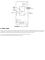
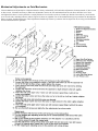
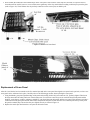
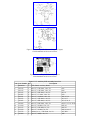
Location of Serial Numbers
Your game's serial number is stamped on all four printed circuit boards, in the locations shown below. The same number is also stamped on
the label located on the rear of the back box. Please mention this number whenever calling your distributor for service.
Location of Serial Numbers
WARRANTY
Seller warrants that its printed circuit boards and parts thereon are free from defects in material and workmanship under normal use and
service for a period of ninety (90) days from date of shipment. Seller warrants that its television monitors (in games supplied with monitors)
are free from defects in material and workmanship under normal use and service for a period of thirty (30) days from date of shipment. None
of the Seller's other products or parts thereof are warranted.
It the products described in this manual fail to conform to this warranty, Sellers' sole liability shall be, at its option, to repair, replace, or credit
Buyer's account for such products which are returned to Seller during said warranty period, provided:
a. Seller is promptly notified in writing upon discovery by Buyer that said products are defective;
b. Such products are returned prepaid to Seller's plant; and
c. Seller's examination of said products discloses to Seller's satisfaction that such alleged defects existed and were not caused by accident,
misuse, neglect, alteration, improper repair, installation or improper testing.
In no event shall Seller be liable for loss of profits, loss of use, incidental or consequential damages.
EXCEPT FOR ANY EXPRESS WARRANTY SET FORTH IN A WRITTEN CONTRACT BETWEEN SELLER AND BUYER WHICH
CONTRACT SUPERSEDES THE TERMS OF THIS ORDER, THIS WARRANTY IS EXPRESSED IN LIEU OF ALL OTHER
WARRANTIES EXPRESSED OR IMPLIED, INCLUDING THE IMPLIED WARRANTIES OF MERCHANTABILITY AND FITNESS
FOR A PARTICULAR PURPOSE, AND OF ALL OTHER OBLIGATIONS OR LIABILITIES ON THE SELLLER'S PART, AND IT
NEITHER ASSUMES NOR AUTHORIZES ANY OTHER PERSON TO ASSUME FOR THE SELLER ANY OTHER LIABILITIES IN
CONNECTION WITH THE SALE OF PRODUCTS UNDER THIS ORDER.
This document is and contains confidential trade secret information of Atari, Inc.
This document is loaned under confidential custody for the sole purpose of operation, maintenance or repair of Atari equipment and may not
be used by or disclosed to any person for any other purpose whatever, and remains the property of Atari, Inc.
Neither it nor the information it contains may be reproduced, used, or disclosed to persons not having a need to know consistent with the
purpose of the loan, without written consent of Atari, Inc.
Forward to the Table of Contents
Back to the top of the manual
Forward to Chapter 1
Table of Contents
●
Top of Manual
●
Location of Serial Numbers
●
Warranty
●
Table of Contents
●
Table of Figures
●
Table of Tables
I. Chapter 1: Location Setup
A. Inventory of Parts in Shipping Cartons
B. Assembly of Game
1. Assembly of Legs and Back Box
2. Attach Back Box
3. Final Inspection
4. Final Assembly
C. Decription of Game Options
D. Setting the Options
E. Self-Test
F. Volume Adjustment
II. Chapter 2: Game Play
A. Attract Mode
B. Play Mode
1. Game Play and Scoring
2. Tilt Condition
3. Match Option
III. Chapter 3: Maintenance and Adjustments
A. Cleaning
1. Game Cabinet Exterior
2. Playfield
B. Fuse Replacement
C. Coin Mechanism
1. Components on Coin Door
2. Access to Coin Mechanisms
3. Clearing of Coin Path
4. Adjustment of Coin Switch Trip Wire
5. Mechanical Adjustments on Coin Mechanism
6. Lubrication
7. General Troubleshooting Hints
D. Game Controls and Playfield Components
1. Solenoid Fuses
2. Troubleshooting of Playfield Switches Connected in Parallel
E. Gas-Discharge Displays
1. Preliminary Operational Checks
2. Check on +90 and -90 Volts Power Supply Voltages
3. Score Panel Removal and Visual Checks
4. Replacement of Score Panel
5. Removing Display Assembly
6. Installing the Display Assembly
F. Lamp Replacement
1. Playfield Lamps
2. Back Box Lamps
G. Adjustment of Speaker Volume
IV. Chapter 4: Theory of Operation
A. Introduction
B. Components of the Microcomputer System
1. Microprocessing Unit
2. Program Memory
3. Data Memory
4. Memory Output Latches
5. Clock Generator
6. Tri-State Buffers
7. Control Logic
C. Circuit Descriptions
1. Solenoid Driver Circuits
2. Lamp Driver Circuits
3. Switch Sensing Circuit
4. Displays and Display Data
5. Credit and Match/Ball Display Circuit
6. Score Display Circuit
7. Sound Generator and Speaker Driver Circuits
Table of Figures
●
Figure 1: Inventory of Accessories
●
Figure 2: Attaching Legs without Pin Jack
●
Figure 3: Attaching Back Box
●
Figure 4: Final Assembly and Inspection
●
Figure 5: Location of Option Swtiches
●
Figure 6: Location of Playfield Switches and Solenoids
●
Figure 7: Playfield Rubber Sizes
●
Figure 8: Coin Door Assembly
●
Figure 9: Hinging Open the Magnet Gate Assembly
●
Figure 10: Removal of Coin Mechanism
●
Figure 11: Surfaces to Clean inside the Coin Mechanism
●
Figure 12: Removal of Plate Covering Rear of Coin Slot
●
Figure 13: Detail View of Coin Switch and Trip Wire
●
Figure 14: Coin Mechanism, Exploded View
●
Figure 15: Close-up View of Lubrication Point
●
Figure 16: Top View of Score and Match/Credit Display Assembly
●
Figure 17: Removal of Score Panel
●
Figure 18: Score Panel Terminals
●
Figure 19: Line-up of Terminal Pins and Terminal Strips
●
Figure 20: Lower Right Comer of Display Assembly
●
Figure 21: Location of Technician Adjustment for Speaker Volume
●
Figure 22: Functional Block Diagram
●
Figure 23: Block Diagram of Microcomputer System
●
Figure 24: Airborne Avenger Wiring Diagram
●
Figure 25-A: Processor PCB Schematic Diagram
●
Figure 25-B: Processor PCB Assembly Drawing
●
Figure 25-C: Processor PCB Assembly Parts List
●
Figure 26-A: Processor PCB Schematic Diagram
●
Figure 26-B: Processor PCB Assembly Drawing
●
Figure 26-C: Processor PCB Assemmbly Parts List
●
Figure 26-D: Processor PCB Parts List
●
Figure 27-A: Auxiliary PCB Schematic Diagram
●
Figure 27-B: Auxiliary PCB Assembly Diagram
●
Figure 27-C: Auxiliary PCB Assembly Parts List
●
Figure 28-A: Match/Credit PCB Schematic Diagram
●
Figure 28-B: Match/Credit PCB Assembly Drawing
●
Figure 28-C: Match/Credit PCB Assembly Parts List
●
Figure 29-A: Score Panel Drive PCB Schematic Diagram
●
Figure 29-B: Score Panel Drive PCB Assembly Drawing
●
Figure 29-C: Figure 28-C: Score Panel Drive PCB Assembly List
●
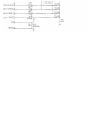
Figure 30: Simplified Diagram of Basic Solenoid Driver Circuit
●
Figure 31: Additional Components to be Installed for Each Metering Function Added
●
Figure 32: Simplified Diagram of Basic Lamp Driver Circuit
●
Figure 33: Simplified Diagram of Switch Sensing Circuit
●
Figure 34: Simplified Diagram of Switch Censing Circuit Waveforms
●
Figure 35: Waveforms for Gas Discharge Displays
●
Figure 36: Arrangement of Connections to Score Panel
Table of Tables
●
Table 1: Self-Test Procedure
●
Table 2: Replay Level Settings
●
Table 3: Maximum Credit Settings
●
Table 4: Switch Identification
●
Table 5: Solenoid Identification
●
Table 6: Coin/Credit Mode Switch Settings
●
Table 7: Replay/Add-a-Ball Switch Settings
●
Table 8: Match Switch Settings
●
Table 9: Slam/Tilt Sound Switch Settings
●
Table 10: "Special" Mode Switch Settings
●
Table 11: AIRBORNE AVENGER Spellout Setting
●
Table 12: Last Ball Bonus Setting
●
Table 13: Fuses Located Near Ball Shooter
●
Table 14: Fuses Located on Power Supply Assembly
●
Table 15: Componenets Required for Special Metering Functions
Back to the top of the manual
Forward to Chapter 1
Up to the table of contents
Forward to Chapter 2
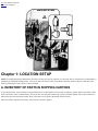
Chapter 1: LOCATION SETUP
NOTE: If reading through this manual does not lead to solving your specific problem, you can reach Atari's Customer Service Department by
telephone (open Monday through Friday, 7:30 a.m. to 4:00 p.m. Pacific Time); From inside California, Alaska or Hawaii: (408) 984-1900
From the remaining 47 states, toll-free: (800) 538-6892
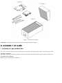
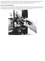
A. INVENTORY OF PARTS IN SHIPPING CARTONS
As you already know, Atari's Airborne Avenger(TM) came to you packaged in one big carton containing 1) game cabinet 2) back box carton,
and 3) accessories carton. Contained in the accessories box were the game cabinet legs, cash box, and this manual. Keys to the coin door are
taped to the top back of the game cabinet. Keys to the back box are taped to the bottom of the back box.
Open the cash box and take an inventory of accessories as shown in Figure 1.
Figure 1: Inventory of Accessories
WARNING: Do not apply power to game until you have inspected inside of cabinet.
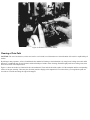
B. ASSEMBLY OF GAME
1. Assembly of Legs and Back Box
First, screw leg levelers (from cash box) into the bottom of each leg. Screw the leg leveler locking nuts onto the leg levelers.
If you have a Pin jackPlace cabinet onto pin jack and raise cabinet at least 2 feet from floor. Then attach all four legs with eight acorn-head bolts.
If you don't have a Pin jackRefer to Figure 2 and follow the instructions.
Figure 2: Attaching Legs without a Pin Jack
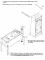
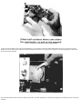
2. Attach Back Box
CAUTION: Back Box carton is labeled "THIS SIDE UP^" Set the Back Box carton as labeled before removing the Back Box from the
carton. This will prevent the Back Box glass from failing out and breaking.
Remove the Back Box and Back Box Key Envelope from the Back Box carton and attach the Back Box to the pin cabinet as instructed in
Figure 3.
Figure 3: Attaching Back Box
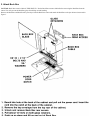
3. Final Inspection
Refer to Figure 4 and follow the instructions.
Figure 4: Final Assembly and Inspection
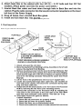
4. Final Assembly
NOTE: The tilt bob is made of a soft material, carbon: don't overtighten.
1. Install the tilt bob (from cash box) onto the pendulum wire at the right front side of the pin cabinet. Tighten the thumbscrew lightly and
leave it pointing toward the coin door. This way it will be accessible from the coin door for fine tuning after the playfield is lowered.
2. Place one ball onto the playfield and the other ball (both from cash box) into the captive ball area (located in the center of the playfield).
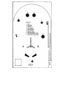
3. Choose the proper instruction cards (from cash box) and attach to the lower arch panel butyrate as illustrated in Figure 5.
4. Install the cash box.
5. Lower the playfield and install the playfield glass (for help, refer to Figure 4).
6. Level the playfield for a 3¡ slope from the rear to the front of the playfield.
7. Insert the power plug into a 115 VAC power source.
C. DESCRIPTION OF GAME OPTIONS
Several options are available for structuring Airborne Avenger(TM) for maximum returns at your location. The following is a list of these
options:
1. Sixteen coin/credit settings for each coin chute
2. Four maximum credit levels
3. Automatic double bonus for last ball or not
4. Match or no match
5. Four different choices for "special" (20,000 points, 30,000 points, free game or extra ball)
6. Three- or five-ball game
7. Add-a-ball or not
8. Replay or no replay
9. Extra ball or 20,000 points for spellout of AIRBORNE AVENGER
D. SETTING THE OPTIONS
WARNING: Power should never be on while setting the options. Dangerous voltages are present inside the game cabinet.
All the options are selectable by merely flipping a switch. Refer to Self-Test Procedure in Table 1. Tables 2, 3, and 6 through 10 list all the
options and the switches necessary to set those options. In these tables, all manufacturer suggested settings are marked with asterisks. Figure 5
shows the location of each switch on the Processor PCB (printed circuit board). To set the switches, lightly press down on the selected switch
toggles with a small pointed object. To set the toggle to on, press on the switch side toward the closest end of the Processor PCB.
Figure 5: Location of Option Switches
E. SELF-TEST
Self-Test is activated by pressing the TEST pushbutton. The TEST pushbutton is located at the inside top middle of the coin door. Pressing the
pushbutton once, begins the lamp test pressing the pushbutton twice, begins the switch test; and the third time, the solenoid test. Pressing the
pushbutton the fourth time causes the game to exit the Self-Test mode and enter the attract mode of operation,
Please read the following Suggestions, then perform the Self-Test Procedure described in Table 1.
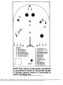
As an aid for locating the playfield switches and solenoids, see Figure 6.
Figure 6: Location of Playfield Switches and Solenoids
NOTE: Toggle 1 of PROG SW1 on Processor PCB should always remain in off position. For bench test purposes, Self-Test mode may be
activated by setting PROG SW1 toggle 1 to on then off. This simulates pressing the TEST pushbutton.
SUGGESTION: Perform Self-Test no less than each time the cash box is collected. Machines in good operating condition have been proven
to earn more money.
SUGGESTION: While performing Self-Test, inspect the playfield for worn rubbers or dirt. Clean the playfield glass and outside of the
cabinet regularly. Clean games attract more players and therefore earn more money
F. VOLUME ADJUSTMENT
The volume control for all game sounds is located inside the cabinet above and to the right of the game speaker To adjust the volume, turn the
volume control clockwise to increase the volume and counter-clockwise to decrease the volume.
A second volume control is located inside the cabinet on the Auxiliary PCB (labeled VOL). This volume control should only be adjusted by a
qualified technician. Technicians may learn the proper adjustment of this control by reading the instructions in the Maintenance chapter
(Chapter 3) of this manual.
Table 1: Self-Test Procedure
Test Name
Test Instruction
Indication of of Test Mode
Test Results
Lamp Test
Press and release (once only)
(Test number) 1 appears in All lamps are lighted (ignore
the TEST pushbutton. (The
4TH UP player score
back boxlamps).
TEST pushbutton is located on display.
High replay level is displayed in
the inside top middle of the
1ST UP player score display.
coin door.)
Medium replay level is
displayed in 2ND UP score
display.
Operator Action
Check to ensure that all
lamps are lighted.
To change, adjust Replay
Rotary switch and PROG
SW1 toggle 4 for the results
as listed in Table 2.
Low replay level is displayed in
3RD UP player score display.
To change, set DIP switch
PROG SW 2 toggle 1 to ON
for 3 balls, OFF for 5 balls.
Maximum credits is displayed To change, set DIP switch
in CREDIT display.
PROG SW 1 toggles 5 and 6
as listed in Table 3.
NOTE: To exit Self-Test,
press and release the TEST
pushbutton three times.
Any activated or stuck switches Identify activated or stuck
are identified by a number in
switches as listed in Table 4.
the CREDIT display. A pulsing NOTE: To exit Self-Test,
tone is heard when a switch is press and release the TEST
activated or stuck.
pushbutton two times.
Each solenoid is individually
Press left flipper button to
energized and identified by a
activate solenoid. Press right
number in the CREDIT display. flipper button to change to
next solenoid. Identify each
solenoid with number in
CREDIT display as listed in
Table 5.
NOTE: To exit Self-Test,
press and release the TEST
pushbutton one time.
Number of balls per game is
displayed in BALL display.
Switch Test
Press and release (once only)
TEST pushbutton.
(Test number) 2 appears in
4TH UP player score
display.
Solenoid Test Press and release (once only)
TEST pushbutton.
(Test number) 3 appears in
4TH UP player score
display.
Table 2 Replay Level Settings
Rotary
PROG SW1 Low Replay Medium Replay High Replay
Switch
Toggle 4
Level
Level
Level
Setting
0
OFF
50,000
70,000
90,000
1
OFF
60,000
90,000
2
OFF
70,000
100,000
3
OFF
80,000
120,000
4
OFF
90,000
130,000
*5
OFF
100,000
150,000
6
OFF
110,000
160,000
7
OFF
120,000
180,000
8
OFF
130,000
190,000
9
OFF
140,000
210,000
10
OFF
150,000
220,000
11
OFF
160,000
240,000
12
OFF
170,000
250,000
13
OFF
180,000
270,000
14
OFF
190,000
280,000
15
OFF
200,000
300,000
0
ON
210,000
310,000
1
ON
220,000
330,000
2
ON
230,000
340,000
3
ON
240,000
360,000
4
ON
250,000
370,000
5
ON
260,000
390,000
6
ON
270,000
400,000
7
ON
280,000
420,000
8
ON
290,000
430,000
9
ON
300,000
450,000
10
ON
310,000
460,000
11
ON
320,000
480,000
12
ON
330,000
490,000
13
ON
340,000
510,000
14
ON
350,000
520,000
15
ON
360,000
540,000
*Indicates manufacturers suggested setting
120,000
130,000
160,000
170,000
200 000
210,000
240,000
250,000
280,000
290,000
320,000
330,000
360,000
370,000
400,000
410,000
440,000
450,000
480,000
490,000
520,000
530,000
560,000
570,000
600,000
610,000
640,000
650,000
680,000
690,000
720,000
Table 3: Maximum Credit Settings
Maximum Credits Prog Sw1 Toggle 5 Prog Sw1 Toggle 6
*8
OFF
OFF
12
ON
OFF
15
OFF
ON
20
ON
ON
*Indicates manufacturers suggested setting
Table 4: Switch identification
Credit Number
Location
1
Left coin switch
2
Right coin switch
3
START pushbutton
4
Coin door slam switch
17
Cabinet slam switch
18
Tilt pendulum
19
Left flipper
20
21
22
23
24
34
35
36
37
38
39
40
41
42
43
44
45
46
47
48
49
50
51
52
56
57
58
59
60
Right flipper
Center target (#4)
Upper right target (#3)
Upper left target (#2)
Lower left target (#1)
Lower ball lane (inside left)
Lower ball lane (middle left)
Lower ball lane (outside left)
Top center ball lane (right)
Top center ball lane (left)
Lower ball lanes
(outside and inside right)
Lower ball lane (middle right)
Left hole kicker
Lower right thumper bumper
Upper right thumper bumper
Upper left thumper bumper
Spinning target
Right eject pocket
Left eject pocket
Right hole kicker
Left slingshot
10 points (5 switches)
50 points (8 switches)
Outhole
Right slingshot
50 and letter advance
Captive ball rollover
Center rollover (B)
Upper right roll-thru
Table 5: Solenoid Identification
Credit Display Number
Solenoid
1
Gate
2
Left flipper
3
Right flipper
4
Outhole
5
Left slingshot
6
Right slingshot
7
Left elect pocket
8
Left hole kicker
9
Right hole kicker
10
Right eject pocket
11
Upper left thumper bumper
12
Upper right thumper bumper
13
Lower right thumper bumper
Table 6: Coin/Credit Mode Switch Settings
Coin/Credit For:
PROG SW2 Toggles
Left Coin Chute Right Coin Chute 3
4
5
6
*1 coin, 1 credit
*1 coin, 1 credit OFF OFF OFF
1 coin, 2 credits
1 coin, 2 credits ON OFF OFF
1 coin, 3 credits
1 coin, 3 credits OFF ON OFF
1 coin, 4 credits
1 coin, 4 credits ON ON OFF
2 coins, 1 credit
2 coins, 1 credit OFF OFF ON
**2 coins, 3 credits **2 coins, 3 credits ON OFF ON
**2 coins, 5 credits **2 coins, 5 credits OFF ON ON
2 coins, 1 credit
1 coin, 1 credit ON ON ON
1 coin, 1 credit
1 coin, 2 credits OFF OFF OFF
1 coin, 2 credits
1 coin, 4 credits ON OFF OFF
1 coin, 3 credits
1 coin, 6 credits OFF ON OFF
**2 coins, 3 credits **2 coins, 7 credits ON ON OFF
**2 coins, 5 credits
1 coin, 5 credits OFF OFF ON
**2 coins, 7 credits
1 coin, 7 credits ON OFF ON
***3 coins, 1 credit
1 coin, 1 credit OFF ON ON
1 coin, 1 credit
1 coin, 3 credits ON ON ON
*Indicates manufacturers suggested setting
**Indicates second coin gives 1 more credit than first coin,
provided no scoring is achieved between coins.
***Indicates no credit until third coin is accepted
Table 7: Replay/Add-A-Ball Switch Settings
Replay/Add-A-Ball for PROG SW1 PROG SW1
Exceeding Replay Score Toggle 7
Toggle 8
No replay, no add-a-ball
OFF
OFF
Add-a-ball
ON
OFF
*Replay
OFF
ON
Replay
ON
ON
*Indicates manufacturers suggested setting
Table 8: Match Switch Setting
PROG SW2
Match
Toggle 2
Match off
OFF
*Match on
ON
*Indicates manufacturers suggested setting
Table 9: Ball Setting
PROG SW2
Balls Per Game
Toggle 1
3 Balls
ON
5 Balls
OFF
Table 10: "Special" Mode Switch Settings
PROG SW2 PROG SW2
"Special Mode"
Toggle 7
Toggle 8
Extra ball for Special
OFF
OFF
*Replay for Special
ON
OFF
OFF
OFF
OFF
OFF
OFF
OFF
OFF
OFF
ON
ON
ON
ON
ON
ON
ON
ON
20,000 points for Special
OFF
ON
20,000 points for Special
ON
ON
*Indicates manufacturers suggested setting
Table 11: AIRBORNE AVENGER Spellout Setting
PROG SW1
Spellout Reward
Toggle 2
Extra Ball Awarded for Spellout
OFF
20,000 Points Awarded for Spellout
ON
Table 12: Last Ball Bonus Setting
PROG SW1
Last Ball Reward
Toggle 3
No Double Bonus for Last Ball
OFF
Double Bonus for Last Ball
ON
Up to the table of contents
Forward to Chapter 2
Up to the table of contents
Back to Chapter 1
Forward to Chapter 3
Chapter 2: GAME PLAY
The game has three modes of operation: attract, play, and Self-Test. The attract mode serves to attract
players to the game. The play mode is active when the game is being played. Self-Test is used by the
operator for game maintenance.
A. ATTRACT MODE
The attract mode is initiated by game power-up, exit from SeIf-Test, or by the end of the previous game.
If entered from power-up or Self-Test, the score and match/credit displays will indicate all eights. If the
attract mode follows a game, the score will indicate the final score of that game. In any case if the game
is untouched, within approximately two minutes the score display will go blank to conserve energy.
In the attract mode, the playfield lamps blink on and off in an exotic light show that attracts potential
players to the game. The game remains in this mode unless a player presses the START pushbutton (if
there are sufficient accumulated credits) or by the operator entering the Self-Test mode by pressing the
TEST pushbutton.
B. PLAY MODE
After a player has depressed the START button, the game responds as follows:
1. The uppermost row in the Score Panel will indicate two zeros, and the words 1ST UP to the right
of the zeros will start to blink on and off.
2. The number in the Credit Display decreases by 1.
3. The Match Display will now become the Ball Display and will indicate 01, meaning that the first
game ball is in play.
4. The ball is ejected from the outhole and rolls over to the ball shooter.
5. The playfield lamps will stop blinking, and 1000 and BALL IN PLAY lamps will be constantly
lighted. All other score-related lamps remain unlighted.
6. The flipper controls are enabled.
7. On the player panel just above and beside the ball shooter, the lamp behind the numeral 1
(surrounded by yellow) will Iight, indicating that so far one player is playing.
Up to this point and even up until the ball hits the first score point object, additional players may be
added to the game. They do this by depositing money (if necessary), and by then depressing the START
pushbutton. Each time the game responds by adding another row of two zeros in the Score Panel,
decreasing the Credit Display by 1, and lighting another lamp just above the ball shooter.
If a ball rolls all the way down to the outhole without achieving any score whatsoever, the outhole kicker
will than eject the bail so that the player can shoot again. But if a ball achieves any score it is counted as
one of the play balls.
As soon as the first score points are earned, the Iock-out coil on the coin door is de-energized and the
coin mechanisms will not accept any coins until after the play sequence ends. The game's speaker also
produces sounds when score points are earned, as follows:
1. For 3000 points, a high-pitch, medium-duration tone, immediately followed by a high-pitch,
medium-duration tone.
2. For 2000 points, a low-pitch, short-duration tone.
3. For 1000 points, a low-pitch, short-duration tone.
4. For 500 points, a high-pitch, long-duration tone.
5. For 100 points, a high-pitch, medium-duration tone.
6. For 50 points, a high-pitch, medium-duration tone.
7. For 10 points, a high-pitch, short-duration tone.
Game Play and Scoring
1. Bonus: Bonus advancement is achieved by hitting the various bonus advance targets, rolling the
ball through one of the two triple bonus advance lanes (when lit), or rolling the ball over one of the
3 single bonus advance lanes (when lit) or by placing the ball into the left eject pocket where the
player receives 2000 pts. and 2 bonus advances for each of "A", "B", and/or " C" lit The bonus has
a maximum advancement of 29,000 points, and is collected at the end of each ball. When double
bonus is achieved, the player collects twice the bonus value he has achieved.
2. Double Bonus: Double bonus is achieved by lighting A, B, and C in the double bonus
accumulator. "A" is lit by shooting the ball into the left hole kicker or the "Lites A" ball lane, "B"
is lit by rolling the ball over the "lites B" rollover or the "lites B" ball lane. "C" is lit by shooting
the ball into the right hole kicker, or by rolling the ball through the "Lites C" ball lanes.
3. Gate: The ball gate is opened by hitting either stand-up target #3 (upper right) or stand-up target #1
(lower Ieft). The gate remains open until the ball goes through the gate or the bail drops into the
outhole.
4. Top Center Ball Lanes: The left and right top center ball lanes are alternately lit, and are changed
by hitting any 50 point switch. Each lane will yield 500 points when not lit, or 3000 points and 3
bonus advances when lit. Rolling through the left lane will light all 3 lower left lanes, and rolling
through the right lane will light all 3 lower right lanes, Rolling through either top center ball lane
will light the captive ball rollover and the "lites B" rollover.
5. Spinner: The spinner target yields 100 pts per rotation or 1000 points per rotation when lit. The
spinner is lit by hitting either the captive-ball target (#4) or the upper left target (#2). The spinner
light goes out when the ball lands in the left eject pocket.
6. A, B, C Bonus: When the ball lands in the left eject pocket, the player collects 500 points plus
2000 points and 2 bonus advances for each of "A", "B", and "C" he has lit in the left eject pocket.
Upon collection, each light is turned out, and the player must relight the letters by achieving the
appropriate rollovers or hole kickers in order to collect them again.
7. Special: The Alternating special is lit when the player lights targets 1 through 4 on a single ball.
The special alternates between the lower left drain, lower right drain, and the upper right roll
through. Both sling shots and the fifty point switches rotate the special. To achieve the special, the
ball must roll over the rollover where the special light is lit.
8. Spell-Out: Completing the Spell-out of AIRBORNE AVENGER can result in either an award of
an extra ball or 20,000 points (see switch options in Table 11). The spell-out is advanced by letter
advance hole kickers, ball lanes, and the triple letter advance roll-thru.
Tilt Condition
The game is provided with a pendulum tilt switch, a slam tilt switch on the coin door, and another
slam-type switch on the floor of the cabinet. if the microcomputer senses any closure of the above
switches, it will put the game into a "tilt" condition and light the TILT lamp. A sound is produced when
the game is tilted.
Match Option
If this is option is selected, after the last player's last ball has reached the outhole the Ball Display
changes into a Match Display (the lamp behind the word BALL will be unlighted and the lamp behind
the word MATCH will light). A random number is selected by the microcomputer. That number is
displayed in the MATCH display.
The microcomputer then compares the match number with the two least significant digits in each player's
score. One game credit will be awarded for each match-up. Therefore a maximum of four matches are
possible after a four-player game has ended.
Up to the table of contents
Back to Chapter 1
Forward to Chapter 3
Up to the table of contents
Back to Chapter 2
Forward to Chapter 4
CHAPTER 3: MAINTENANCE AND ADJUSTMENTS
Due to its solid-state electronic circuitry, this Atari game shouId require very little maintenance and only occasional adjustment. Information
given in this chapter and elsewhere in the manual is intended to cover most servicing situations that may be encountered at the game site. The
procedures given are in sufficient detail to be understood by a person with moderate technical ability.
A. CLEANING
Game Cabinet Exterior
The exterior parts of the game cabinet and glass may be cleaned with any non-abrasive household cleaner. If desired, special coin machine
cleaners which leave no residue can be obtained from distributors.
Playfield
The surface of the playfield has a finish chosen for its long-wearing property. Check the surface periodically to make sure that it is both clean
and free of foreign material. Also, periodically check the ball to make sure that it also is smooth and clean. Immediately replace any ball that
is chipped, burred, corroded, or pitted. A defective ball will cause damage to the playfield surface in a very short time.
Much of the player appeal in pinball games depends on smooth ball travel over the entire playfield. To keep the playfield and ball from
wearing out prematurely, Atari recommends using only a nonabrasive cleaner.
Do not use such products as "Formula 409" or "Windex," kitchen cleansers, soapy cleaning pads or steel wool, waxes or polishes, or great
amounts of water. These products may easily scour and damage the silk-screened artwork, and/or cause buildup of gummy residue.
While cleaning the playfield, avoid getting foreign material into the bodies of the star rollovers. You might cover the switch body with a small
amount of masking tape when cleaning around the switch body.
For replacement sizes of playfield rubbers, see Figure 7.
Figure 7: Playfield Rubber Sizes
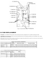
B. FUSE REPLACEMENT
WARNING: As an additional safety measure when replacing fuses always unplug the power cord before opening the cabinet.
CAUTION: When changing fuses make sure that the replacement fuses have tine ratings specified by Atari, and that the fuse is being
replaced in the correct fuse holder.
Replacement fuse values are listed on charts near both the power supply fuse panel and service panel. In case these fuse value charts have
been destroyed, refer to Tables 13 and 14 for the values.
Table 13: Fuses Located Near Ball Shooter
Circuit
Position on Strip Designation
Domestic Fuse Rating
Foreign Fuse Rating
Protected
Uppermost fuse F7
Back Box
2 amps, 250 volts, fast-blo (3AG) 2 amps, 250 volts, fast-blo (3AG)
Middle fuse
F8
Line Power 7 amps, 250 volts, slo-blo (3AG) 2.5 amps, 250 volts, slo-blo (3AB)
Bottom fuse
F9
Service Outlet 2 amps, 250 volts, fast-blo (3AG) 2 amps, 250 volts, fast-blo (3AG)
Table 14: Fuses Located on Power Supply Assembly
Circuit
Position on Strip Designation
Rating
Protected
Uppermost fuse F6
Audio
2 amps, 250 volts, fast-blo (3AG)
F5
Displays 0.5 amps, 250 volts, slo-blo (3AG)
F4
Displays 0.5 amps, 250 volts, slo-blo (3AG)
F3
Lamps
15 amps, 250 volts, fast-blo (3AB)
Bottom fuse
F2
F1
Logic
7 amps, 250 volts, slo-blo (3AG)
Solenoids 15 amps, 250 volts, fast-blo (3AB)
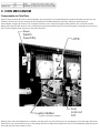
C. COIN MECHANISM
Components on Coin Door
Figure 8 shows the back side of the coin door assembly where the game's two coin mechanisms are mounted. Included is the lock-out coil
assembly; the Iock-out wires are connected to this assembly but are hidden behind the coin mechs. During the attract mode, the
microcomputer energizes the lock-out coil, causing the lock-out wires to retract far enough to allow genuine coins to reach the coin box.
During play mode (and also when AC power in the game has been turned off) the lock-out coil is de-energized, causing the Iock-out wires to
move out far enough to divert coins over to the coin return chute.
Figure 8: Coin Door Assembly
Directly below each coin mechanism is a secondary coin chute and a coin switch with a trip wire extending out to the front edge of the chute.
When the trip wire is positioned correctly, a coin passing down the secondary chute and into the coin box will momentarily push the trip wire
down and cause the switch contacts to close.
Also shown in the photograph is a slam switch assembly. It has been included to defeat any players who might try to obtain free credits by
violently pounding on the coin door to momentarily close the contacts on a coin switch. The slam switch contacts connect to the
microcomputer system, which will ignore coin switch signals whenever the slam switch contacts are closed.
Access to Coin Mechanisms
To remove jammed coins, and for maintenance cleaning, each magnet gate assembly can be hinged open without removing it from the door,
as shown in Figure 9. Or, if necessary, each coin mechanism can be entirely removed from the door merely by pushing down on a release
lever and simultaneously tilting the mechanism back, then lifting it up and out. This is shown in Figure 10.
Figure 9: Hinging Open the Magnet Gate Assembly
Figure 10: Removal of Coin Mechanism
Clearing of Coin Path
CAUTION: The use of an abrasive (such as steel wool or a wire brush) or a lubrication on a coin mechanism will result in a rapid buildup of
residue.
By talking to many operators, we have found that the best method of cleaning a coin mechanism is by using hot or boiling water and a mild
detergent. A toothbrush may be used for those stubborn buildups of residue. After cleaning, flush thoroughly with hot or boiling water, then
blow out all water with compressed air.
Figure 11 shows the surfaces to clean inside the coin mechanism. These include the inside surface of of the mainplate and the corresponding
surface of the gate assembly. There may also be metal particles clinging to the magnet itself. To remove these you can guide the point of a
screwdriver or similar tool along the edge of the magnet.
Figure 11: Surfaces to Clean inside the Coin Mechanism
If coins are not traveling as far as the coin mechanisms, you will need to clean the channel beneath the coin slot. To gain access to this
channel, use a 3/8-inch wrench and remove all three nuts that secure the cover plate (refer to Figure 12). Removing the plate will provide
access to the entire channel.
Figure 12: Removal of Plate Covering Rear of Coin Slot
Also clean the inside surfaces of the secondary coin chutes, but when doing this be careful not to damage or bend the trip wires on the coin
switches.
Adjustment of Coin Switch Trip Wire
In order for a coin switch to operate reliably when a coin travels down the secondary coin chute, the rest position of the switch's trip wire
should be as shown in Figure 13. Use extreme care when handling or touching these wires.
Three problems can occur with trip wires-they can be too long, too short, or become loosened and fall off.
With a too long wire you may have a problem of it catching on the opening in the cash box as a coin is accepted. You can cut off the end of
the wire in small increments, making sure it still extends slightly through the "V" of the coin chute.
If the trip wire is too short (either by wrong adjustment or by being cut off too much), then coins may slip by the wire without tripping it, and
no credits will be given. The solution is to carefully bend and somewhat straighten out the wire to lengthen it. If you cannot straighten it
enough, then you will have to contact your distributor to order another trip wire.
If the wire is loose and falls off of its mounting stud, it will also cause no credits to be given. Secure the wire by crimping together both ends
of the brass-colored mounting stud with a pair of pliers (also see Figure 13). If you should ever need to remove the trip wire, the two halves of
the mounting stud can be separated with a small screwdriver.
Figure 13 Detail View of Coin Switch and Trip Wire
Mechanical Adjustments on Coin Mechanism
Coin mechanisms are adjusted prior to shipment from the factory and normally will retain these adjustments for many months. If, due to wear
or other causes, it becomes necessary to make new adjustments, remove the coin mechanism from the coin door, then take it to a clean
well-lighted area where it can be placed in a vertical position on a level surface (such as a bench top). Besides a screwdriver you will need a
set of several coins, including both new and old. Figure 14 shows an exploded view of the mechanism and gives procedures for adjusting the
kicker, separator, and the magnet gate. These adjustments should only be done by someone who has experience in servicing coin mechanisms
and who understands their operation.
Figure 14: Coin Mechanism, Exploded View
Lubrication
Do not apply lubrication to the coin mechanisms. The only points that may need lubrication (and only rarely) are the shafts of the scavenger
buttons (coin rejection buttons) where they pass through the coin door. Apply only one drop of light machine oil, and be positive that no oil
drops down onto a coin mechanism. Figure 15 shows this lubrication point.
Figure 15: Close-up View of Lubrication Point
General Troubleshooting Hints
The first action is to look for jammed coins. After these have been removed examine the coin path for presence of foreign material or loose
objects (such as chewing gum, small metallic objects, paper wads, etc.). In cases where game usage is heavy, it may be necessary to clean the
entire coin path periodically, in order to prevent build-up of contaminants that can hinder the movement of coins through the mechanism. Also
confirm that the trip wire on each coin switch is intact, and is properly adjusted. If troubles still persist, check the conditions and positions of
the lock-out wires, and the mechanical adjustments on the coin mechanisms before suspecting the electronics. If a coin mechanism rejects
genuine coins, try to readjust it. If this is not successful, then replace it with a working mechanism.
Correct operation of the slam switch can be verified by putting the game into the test mode and performing the switch test (described in Table
1). Correct operation of the other switches and of the Iock-out coil can also be checked by the switch test, or else merely by manually
operating them and watching game responses as it changes from the attract mode to play mode, and then back to attract mode again.
D. GAME CONTROLS AND PLAYFIELD COMPONENTS
Opening the cabinet and raising the playfield will give access to the playfield components and the game controls -- START pushbutton
switch, flipper switches, pendulum tilt and cabinet tilt switches, Power On/Off Switch, speaker, and the ball shooter.
The game's microcomputer system improves game reliability and significantly reduces maintenance requirements because it replaces
conventional electromechanical devices such as step-up rotary switches and motorized trip relay banks. Another game feature is that
adjustment-free sealed-contact switches replace all open-contact blade-type switches.
Solenoid Fuses
Plugged onto connector J8 on the Processor PCB is a special miniature PCB assembly that provides individual fuses for each solenoid line.
This assembly is identified by the Atari part number A020383. These fuses have been added to prevent the driver transistor from overheating
and damaging the surface of the PCB if current flow starts to exceed the maximum fused value.
Whenever a fuse is found to be open, perform the following two checks before replacing the fuse. After making sure that AC power to the
game is shut off, first use an ohmmeter to measure the solenoid's DC resistance. Flipper solenoids should have a DC resistance of
approximately 7.7 ohms. Hole kickers should have a DC resistance of approximately 18 ohms. The gate solenoids should read approximately
200 ohms with ohmmeter connected in one direction and about 15 ohms with the instrument connected in other direction. Secondly, use the
ohmmeter to check the collector-emitter junction of the 2N6044 driver transistor.
Replace only with 2 amp, 125 volts, slo-blo (3AG) fuses.
Troubleshooting of Playfield Switches Connected In Parallel
As described in Chapter 1, Section D, you can use the switch test both for automatically detecting switches with stuck contacts and for
manually identifying switches with stuck contacts and for manually identifying switches whose contacts are not closing properly. But in the
instance where contacts from two switches are connected in parallel, additional troubleshooting steps will be needed in order to verify whether
or not a given switch is defective.
For example, switch test #39 simultaneously checks both inside and outside right lower ball lanes. To confirm whether just one or else both
switches are defective, one at a time you must temporarily unsolder the wire to the normally open contact of each switch, while leaving the
other switch still connected then perform the switch test separately for each switch connected alone.
Wiring connections to the playfield switches are shown in Chapter 4 in the Wiring Diagram, Sheet 2.
E. GAS-DISCHARGE DISPLAYS
The displays are designed to be maintenance free, so they normally require attention only if incorrect operation is observed. Use the following
procedures to isolate and correct problems with the displays.
Preliminary Operational Checks
Make sure that the coin door is closed and locked, Then plug in the power cord and place the Power On/Off Switch in its on position.
Immediately after AC power is applied, the Score Display should be showing all 8s and the PLAYER UP indications 1ST UP, 2ND UP, etc.)
light one at a time, in numerical sequence. All 8s should be showing in the Credit Display and the Match/Ball Display.
The displays are all operating properly if every display segments lights up at least once. But if one or more segments remain dark, isolate the
problem circuitry as described in the following subsection.
Check on +90 and -90 Volts Power Supply Voltages
Remove the playfield glass, then remove the lower arch panel. Troubleshoot the displays as follows:
WARNING: Whenever AC power is applied to the game, voltage potential differences as large as 180 volts are present at the bare terminals
of the score panel's edge connector J21, and at various other points on both printed circuit boards.
1. Defeat the Interlock Safety Switch by pulling all the way out on the switch's spring-loaded plunger.
2. Place the Power On/Off Switch in the on position.
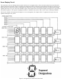
3. Connect a voltmeter across the following capacitors shown in Figure 16, and check for the readings listed below:
On Match/Credit Display PCB, place meter's ground lead on "plus" side of C2; other lead placed on "pIus" side of C1 gives +90 volts
reading, and on "minus" side of C2 gives -90 volts reading.
On Score Panel PCB, place ground lead on "plus" side of C2; other lead on "plus" side of C1 gives +90 volts reading, and on "minus"
side of C2 gives -90 volts reading.
4. If one or more readings are low (or at zero volts), check each PCB separately as follows. Disconnect J19 and re-measure the voltages on
the Score PCB. If the voltages are OK, then some portion of the circuitry on the Match/Credit Display PCB is pulling down the supply
voltages. If the voltages are still incorrect, reconnect J19, disconnect J17, and re-measure the voltages on the Match/Credit Display
PCB. If voltages are OK, then some portion of the circuitry on the Score Display PCB is pulling down the supply voltages.
If the voltages remained incorrect while each board was checked separately, leave J17 and J19 both disconnected. Then check the +90
volt and -90 volt outputs on the Auxiliary PCB (where the high voltage power supply circuitry is located). These 90-volt supply
voltages must both be present on each display PCB before the displays can light up.
If all voltage readings on the display PCBs are within 5% of the correct values, then go on to the next portion of the procedure.
Figure 16: Top View of Score and Match/Credit Display Assembly
Score Panel Removal and Visual Checks
After the +90 volt and -90 volt supply voltages have been verified, the next troubleshooting step on the score panel will be to remove it from
connector J21.
1. Turn off AC power to the game, preferably by pulling out the power plug from the wall outlet.
2. Remove the metal clips holding the score panel onto the bracket arms of J21 (refer to Figure 17).
WARNING: Glass edges of score panel may be sharp. Use caution to prevent cutting your hands.
3. Using your right band, grasp the right edge of the score panel. Carefully lift it up approximately 1/4-inch, and then pull it straight out
and remove it completely.
4. Examine the positions of the terminal pins on J21. Tips of the pins should be aligned in the same plane, as shown in the detail view of
Figure 17. If not bent out of alignment, all pins can then make contact with the score panel's terminal strips when the panel is plugged
in.
5. Next examine the condition of the terminal strips on the score panel. If the surfaces of the strips are corroded, use a pencil eraser to
clean them off. Be careful, however, not to rub the eraser against any of the tiny metal ribbons touching certain strips up near the glass
(refer to Figure 18). These ribbons must be perfectly centered over the correct pins, not halfway off.
Figure 17: Removal of Score Panel
Figure 18: Score Panel Terminals
Replacement of Score Panel
After the visual checks have been made on the J21 terminal pins and on the score panel the original score panel can be put back, or else a new
score panel can be substituted in its place, Carefully observe the following procedure when replacing the score panel.
1. Using both hands, grasp tine right-hand edge of the panel and carefully slide it fully into connector J21, perfectly aligned. Then lower
the edge down until the entire panel rests in the bracket arms. You will note some free space on each side between the panel and the
brackets. At the factory a rubbery substance called RTV was placed between the bracket and the score panel. This substance provides a
cushion between the glass panel and the metal arms, and positions the panel so that connector J21's terminal pins line up exactly with
the panel's terminal strips. Be sure that they are aligned correctly as shown in Figure 19.
2. Replace the metal clips that fasten the score panel to the bracket arms.
Figure 19: Line-up of Terminal Pins and Terminal Strips
Removing Display Assembly
Certain portions of the PCBs are accessible for troubleshooting when the display assembly is left mounted on the playfield. However, to gain
access to the remaining portions, or to replace components or an entire PCB, use the following procedure.
1. Turn off AC power to the game, preferably by pulling out the power plug.
2. Disconnect connectors J17, J18, J19, and J20.
3. Use a Phillips-head screwdriver to loosen the four screws that fasten the display assembly to the playfield, and then remove the screws.
4. Lift the entire assembly up and remove it from the playfield.
Installing the Display Assembly
After repair and/or replacement of the display boards and displays, use the following procedure to re-attach the assembly to the playfield.
1. Lower the assembly down into its final position and line up the four mounting holes with their mating holes in the playfield. Be careful
not to pinch the lamp wires that are routed through a slot at the lower right corner of the assembly (refer to Figure 20).
2. Insert the four mounting screws and use a Phillips-head screwdriver to tighten them down.
3. Connect connectors J17, J18, J19, and J20.
Figure 20: Lower Right Corner of Display Assembly
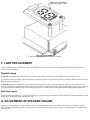
F. LAMP REPLACEMENT
To insure continued player appeal to the game, you should periodically check for burned-out playfield and back box lamps, and replace
defective ones immediately.
Playfield Lamps
CAUTION: When replacing playfield lamps use #47 bulbs only; other bulb types may cause damage to the lamp driver circuits.
If you suspect a burned out lamp, replace lamp with in neighboring "known to be good" lamp. This will establish whether the lamp is bad or a
bad lamp socket or lamp driver.
WARNING: Make sure game power is turned off before replacing lamps. This is especially important if the lower arch panel has to be
removed to gain access to the lamps beneath it. Whenever AC power is applied to the game, voltage potential differences as large as 180 volts
are present at the bare terminals of the score panel's edge connector J21, and at various other points on both display printed circuit boards.
Back Box Lamps
When replacing these lamps use 7.5-watt bulbs. If the lamp is to flash on and off, remember to place a flasher unit (button-shaped disc) in the
socket before inserting and tightening down the bulb.
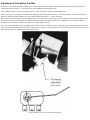
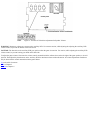
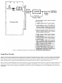
G. ADJUSTMENT OF SPEAKER VOLUME
Airborne Avenger contains two volume controls. One is conveniently mounted inside the cabinet so the operator may adjust the volume
without raising the playfield. The other volume control is mounted on the Auxiliary PCB (see Figure 21) and should never be adjusted after
being set once.
Figure 21: Location of Technician Adjustment for Speaker Volume
WARNING: Dangerous voltages are present on the Auxiliary PCB. Use extreme caution, while adjusting the adjusting the Auxiliary PCB
volume control, to prevent the hazard of electrical shock.
CAUTION: The heat sink on the Auxiliary PCB gets quite hot when the game is turned on. Use caution, while adjusting the Auxiliary PCB
volume control, to prevent burning your hand on this heat sink.
To adjust the game volume, first rotate the volume control, mounted inside the cabinet above and to the right of the game speaker, to its mid
position. Then adjust the potentiometer on the Auxiliary PCB for maximum volume without distortion. All volume adjustments should now
only be done with the control mounted inside the game cabinet.
Up to the table of contents
Back to Chapter 2
Forward to Chapter 4
Up to the table of contents
Back to Chapter 3
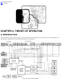
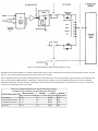
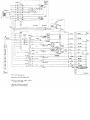
CHAPTER 4: THEORY OF OPERATION
A. INTRODUCTION
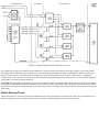
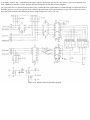
The block diagram in Figure 22 shows the game's major functional elements and depicts their interconnections. The central element is the
microcomputer, which consists of a microprocessor, memories and control logic.
Figure 22: Functional Block Diagram
By means of a switch sensing circuit, the player operated switches, playfield switches and operator option switches produce switch data for
the microcomputer. Switch closures occur when a player deposits money in the game, depresses the START pushbutton, operates the ball
shooter so the ball goes onto the playfield and interacts with playfield objects, and depresses the flipper buttons. Switch Closures also result
when a player tilts the game. Executing the instructions stored in the preprogrammed portion of its memory, the microcumpter then responds
to the switch data by energizing various solenoids, lighting various lamps, and producing sound data for the speaker and display data for the
Score, Credit and Ball/Match Displays.
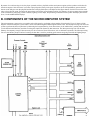
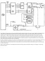
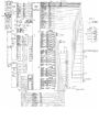
B. COMPONENTS OF THE MICROCOMPUTER SYSTEM
The microcomputer system carries out complex tasks of the game by performing a large number of simple tasks. Figure 23 shows a block
diagram of the microcomputer system and its various interconnecting data, addressing and control buses. The Microprocessing Unit causes the
system to perform the desired operations by addressing the Program Memory for an instruction (via the Address Bus), reading that instruction
(via the bidirectional Data Bus), and then executing the simple task dictated by that instruction. The Microprocessing Unit uses the Data
Memory for temporary storage of data necessary for the execution of future instructions, such as arithmetic operations. The Microprocessing
Unit uses the Memory Output Latches for storing the data that is used for producing game sounds energizing solenoids and lighting lamps.
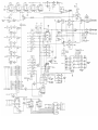
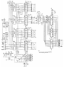
Figure 23: Block Diagram of Microcomputer System
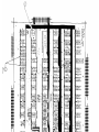
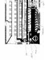
Figure 24: Airborne Avenger Wiring Diagram (2 pages)
Click thumbnails for full-sized versions.
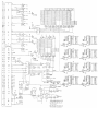
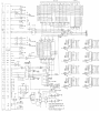
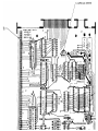
The following paragraphs describe the game's microcomputer system in more detail. The drawing references are to the Processor PCB
schematic shown in Figures 25 and 26.
Figure 25-A: Processor PCB Schematic Diagram (4 pages)
Click thumbnails for full-sized versions.
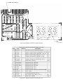
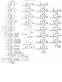
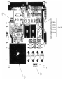
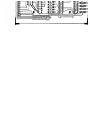
Figure 25-B: Processor PCB Assembly Drawing
Click thumbnail for full-sized version.
Item
1
2
3
4
5
6
7
8
9
10
Part Number
006021-01
10-5201
10-5471
10-5102
10-5822
10-5223
10-5105
Figure 25-C: Processor PCB Assembly Parts List
Qty.
Description
1
Printed Circuit Board
15 Res., Car Comp., 1/4W, 5% 200 OHM R6-11, 13-20, 23
5
Res., Car Comp., 1/4W, 5% 470
R27-29, 31, 32
7
Res., Car Comp., 1/4W, 5% 1K
R2-5, 26, 33, 36
1
Res., Car Comp., 1/4W, 5% 8.2K
R35
1
Res., Car Comp., 1/4W, 5% 22K
R34
1
Res., Car Comp., 1/4W, 5% 1M
R30
19-007
19-808W4P0
2
1
Res., Network 10K
Res., Wirewound, 1OW, 4 OHM
A3/4, A4/5
R1
11
12
13
14
15
16
17
18
19
20
21
22
23
24
25
26
27
28
29
30
31
32
33
34
35
36
24-250227
27-250104
28-101390
28-101151
29-006
29-007
1
27
3
1
1
1
Cap, Elecrolytic, 220uf, 25V
Cap, Ceramic, 0.1uf, 25V
Cap, Mica, 39pf, 100V
Cap, Mica, 150pf, 100V
Cap, Tantalum, 1uf, 35V
Cap, Tantalum, 22uf, 15V
C2
C3, 5, 9-33
C4, 6, 8
C7
C1
C34
31-1N914 Diode,
32-P6KE18
34-2N6044
34-2N3643
37-7400
37-7402
37-7403
37-7404
37-74L04
37-7407
37-7408
37-74LS08
37-7414
37-7420
37-7427
37-7432
37-7437
37-7474
16
1
15
1
3
2
1
2
1
4
3
2
3
1
1
1
1
2
1N914
Diode, Transient Supp. P6KE18
Transistor, 2N6044
Transistor, 2N3643
I.C. 7400
I.C. 7402
I.C. 7403
I.C. 7404
I.C. 74L04
I.C. 7407
I.C. 7408
I.C. 74LS08
I.C. 7414
I.C. 7420
I.C. 7427
I.C. 7432
I.C. 7437
I.C. 7474
37
37-7493
10
I.C. 7493
38
37-74145
8
I.C. 74145
39
40
41
42
43
37-74157
37-8097
37-9301
37-9316
37-9321
1
2
2
2
1
I.C. 74157
I.C. 8097
I.C. 9301
I.C. 9316
I.C. 9321
44
37-9334
8
I.C. 9334
45
46
37-9602
37-LM323
1
1
I.C. 9602
Regulator LM323
CR2-16, 19
CR1
Q1-8, 11-13, 15-17, 20
Q21
D10, A1, F1
A2, C7
D9
D4, E10
D11
D14, D16,D18, D20
B2, D2, D3
B/C8, C/D8
B11, C9,E9
B8
B7
C8
C10
B6, B9
A6, A7, A8, A9, A10,
A11, B3, C11,E12, E13
F3, F5, F6, F9,
F10, F11, F12, F13
B5
C4, C5
C6, E11
B4, D13
D1
C13, Cl4, C15, C16,
C17, Cl8, Cl9, C20
B10
47
37-MC1413
10
I.C. MC1413 (2003A)
48
49
50
51
52
53
54
55
56
57
58
59
37-MC14050
3
I.C. MC14050
62-001
66-118P1T
66-12FP1T
72-1608S
75-016
75-056
75-916C
78-06001
78-16005
1
2
1
2
2
2
2
1
1
Switch, Push Button SPST
Switch, Dip, 8 Position
F2, F4
Switch, Hex
Screw, Mach., Pan Hd. Phil. #6-32 x 1/2"
Washer, Flat #6
Washer, Lock, Int. Tooth #6
Nut, Hex #6-32
Heatsink, LM323
Silpad
A16, A17, A18, A19, A20,
B16, B17, B18, B19, B20
A3, A4, A5
60
61
62
63
64
65
66
67
68
69
70
71
72
73
74
75
76
77
79-42040
79-58122
90-108
90-6001
90-7015
1
1
1
1
2
Socket, 40 Position, Med Insertion
Header, 4 Pin
Crystal, 4.000 MHZ
I.C.
Ram, 2111A
C1
J9
Y1
C1
D5, D8
020244-01
020250-01
020245-01
020251-01
020247-01
020248-01
020246-01
020249-01
020252-01
1
1
1
1
1
1
1
1
1
Program Prom 1LSB
Program Prom 1MSB
Program Prom 2LSB
Program Prom 2MSB
Program Prom 3LSB
Program Prom 3MSB
Program Prom 4LSB
Program Prom 4MSB
Audio Prom
E1
E7
E2
E8
E4
E5
E3
E6
D12
Figure 25-C: Processor PCB Assembly Parts List
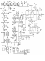
Figure 26-A: Processor PCB Schematic Diagram (4 pages)
Click thumbnail for full-sized version.
Figure 26-B: Processor PCB Assembly Drawing
Click thumbnail for full-sized version.
Item
1
2
3
4
5
6
7
8
9
10
11
12
13
14
15
16
17
18
19
20
21
22
23
24
25
26
27
Part Number
006021-01
10-5201
10-5471
10-5102
10-5822
10-5223
10-5105
Figure 26-C: Processor PCB Assembly Parts List
Qty.
Description
1
Printed Circuit Board
15 Res., Car Comp., 1/4W, 5% 200 OHM R6-11, 13-20, 23
5
Res., Car Comp., 1/4W, 5% 470
R27-29, 31, 32
7
Res., Car Comp., 1/4W, 5% 1K
R2-5, 26, 33, 36
1
Res., Car Comp., 1/4W, 5% 8.2K
R35
1
Res., Car Comp., 1/4W, 5% 22K
R34
1
Res., Car Comp., 1/4W, 5% 1M
R30
19-007
19-808W4P0
2
1
Res., Network 10K
Res., Wirewound, 1OW, 4 OHM
A3/4, A4/5
R1
24-250227
27-250104
28-101390
28-101151
29-006
29-007
1
27
3
1
1
1
Cap, Elecrolytic, 220uf, 25V
Cap, Ceramic, 0.1uf, 25V
Cap, Mica, 39pf, 100V
Cap, Mica, 150pf, 100V
Cap, Tantalum, 1uf, 35V
Cap, Tantalum, 22uf, 15V
C2
C3, 5, 9-33
C4, 6, 8
C7
C1
C34
31-1N914 Diode,
32-P6KE18
34-2N6044
34-2N3643
37-7400
37-7402
37-7403
37-7404
37-74L04
16
1
15
1
3
2
1
2
1
1N914
Diode, Transient Supp. P6KE18
Transistor, 2N6044
Transistor, 2N3643
I.C. 7400
I.C. 7402
I.C. 7403
I.C. 7404
I.C. 74L04
CR2-16, 19
CR1
Q1-8, 11-13, 15-17, 20
Q21
D10, A1, F1
A2, C7
D9
D4, E10
D11
28
29
30
31
32
33
34
35
36
37-7407
37-7408
37-74LS08
37-7414
37-7420
37-7427
37-7432
37-7437
37-7474
4
3
2
3
1
1
1
1
2
I.C. 7407
I.C. 7408
I.C. 74LS08
I.C. 7414
I.C. 7420
I.C. 7427
I.C. 7432
I.C. 7437
I.C. 7474
D14, D16,D18, D20
B2, D2, D3
B/C8, C/D8
B11, C9,E9
B8
B7
C8
C10
B6, B9
A6, A7, A8, A9, A10,
A11, B3, C11,E12, E13
F3, F5, F6, F9,
F10, F11, F12, F13
B5
C4, C5
C6, E11
B4, D13
D1
C13, Cl4, C15, C16,
C17, Cl8, Cl9, C20
B10
37
37-7493
10
I.C. 7493
38
37-74145
8
I.C. 74145
39
40
41
42
43
37-74157
37-8097
37-9301
37-9316
37-9321
1
2
2
2
1
I.C. 74157
I.C. 8097
I.C. 9301
I.C. 9316
I.C. 9321
44
37-9334
8
I.C. 9334
45
46
37-9602
37-LM323
1
1
I.C. 9602
Regulator LM323
47
37-MC1413
10
I.C. MC1413 (2003A)
48
49
50
51
52
53
54
55
56
57
58
59
60
61
62
63
64
65
66
67
68
69
70
71
72
73
74
75
76
37-MC14050
3
I.C. MC14050
62-001
66-118P1T
66-12FP1T
72-1608S
75-016
75-056
75-916C
78-06001
78-16005
1
2
1
2
2
2
2
1
1
Switch, Push Button SPST
Switch, Dip, 8 Position
F2, F4
Switch, Hex
Screw, Mach., Pan Hd. Phil. #6-32 x 1/2"
Washer, Flat #6
Washer, Lock, Int. Tooth #6
Nut, Hex #6-32
Heatsink, LM323
Silpad
79-42040
79-58122
90-108
90-6001
90-7015
1
1
1
1
2
Socket, 40 Position, Med Insertion
Header, 4 Pin
Crystal, 4.000 MHZ
I.C.
Ram, 2111A
C1
J9
Y1
C1
D5, D8
020244-01
020250-01
020245-01
020251-01
020247-01
020248-01
020246-01
020249-01
1
1
1
1
1
1
1
1
Program Prom 1LSB
Program Prom 1MSB
Program Prom 2LSB
Program Prom 2MSB
Program Prom 3LSB
Program Prom 3MSB
Program Prom 4LSB
Program Prom 4MSB
E1
E7
E2
E8
E4
E5
E3
E6
A16, A17, A18, A19, A20,
B16, B17, B18, B19, B20
A3, A4, A5
77
78
79
80
020252-01
1
Audio Prom
D12
37-74S00
2
I.C. 74S00A
F0, F1
Figure 26-C: Processor PCB Assembly Parts List
Figure 26-D: Processor PCB Parts List
Description
Printed Circuit Board
Res., Car Comp., 1/4W, 5% 200 OHM
Res., Car Comp., 1/4W, 5% 470
Res., Car Comp., 1/4W, 5% 1K
Res., Car Comp., 1/4W, 5% 8.2K
Res., Car Comp., 1/4W, 5% 22K
Res., Car Comp., 1/4W, 5% 1M
Item
1
2
3
4
5
6
7
8
9
10
11
12
13
14
15
16
17
18
19
20
21
22
23
24
25
26
27
28
29
30
31
32
33
34
35
36
Part Number
006021-01
10-5201
10-5471
10-5102
10-5822
10-5223
10-5105
Qty.
1
15
5
7
1
1
1
19-007
19-808W4P0
2
1
Res., Network 10K
Res., Wirewound, 1OW, 4 OHM
A3/4, A4/5
R1
24-250227
27-250104
28-101390
28-101151
29-006
29-007
1
27
3
1
1
1
Cap, Elecrolytic, 220uf, 25V
Cap, Ceramic, 0.1uf, 25V
Cap, Mica, 39pf, 100V
Cap, Mica, 150pf, 100V
Cap, Tantalum, 1uf, 35V
Cap, Tantalum, 22uf, 15V
C2
C3, 5, 9-33
C4, 6, 8
C7
C1
C34
31-1N914 Diode,
32-P6KE18
34-2N6044
34-2N3643
37-7400
37-7402
37-7403
37-7404
37-74L04
37-7407
37-7408
37-74LS08
37-7414
37-7420
37-7427
37-7432
37-7437
37-7474
16
1
15
1
3
2
1
2
1
4
3
2
3
1
1
1
1
2
1N914
Diode, Transient Supp. P6KE18
Transistor, 2N6044
Transistor, 2N3643
I.C. 7400
I.C. 7402
I.C. 7403
I.C. 7404
I.C. 74L04
I.C. 7407
I.C. 7408
I.C. 74LS08
I.C. 7414
I.C. 7420
I.C. 7427
I.C. 7432
I.C. 7437
I.C. 7474
37
37-7493
10
I.C. 7493
38
37-74145
8
I.C. 74145
39
40
41
37-74157
37-8097
37-9301
1
2
2
I.C. 74157
I.C. 8097
I.C. 9301
CR2-16, 19
CR1
Q1-8, 11-13, 15-17, 20
Q21
D10, A1, F1
A2, C7
D9
D4, E10
D11
D14, D16,D18, D20
B2, D2, D3
B/C8, C/D8
B11, C9,E9
B8
B7
C8
C10
B6, B9
A6, A7, A8, A9, A10,
A11, B3, C11,E12, E13
F3, F5, F6, F9,
F10, F11, F12, F13
B5
C4, C5
C6, E11
R6-11, 13-20, 23
R27-29, 31, 32
R2-5, 26, 33, 36
R35
R34
R30
42
43
37-9316
37-9321
2
1
I.C. 9316
I.C. 9321
44
37-9334
8
I.C. 9334
45
46
37-9602
37-LM323
1
1
I.C. 9602
Regulator LM323
47
37-MC1413
10
I.C. MC1413 (2003A)
48
49
50
51
52
53
54
55
56
57
58
59
60
61
62
63
64
65
66
67
68
69
70
71
72
73
74
75
76
77
78
79
80
37-MC14050
3
I.C. MC14050
62-001
66-118P1T
66-12FP1T
72-1608S
75-016
75-056
75-916C
78-06001
78-16005
1
2
1
2
2
2
2
1
1
Switch, Push Button SPST
Switch, Dip, 8 Position
F2, F4
Switch, Hex
Screw, Mach., Pan Hd. Phil. #6-32 x 1/2"
Washer, Flat #6
Washer, Lock, Int. Tooth #6
Nut, Hex #6-32
Heatsink, LM323
Silpad
79-42040
79-58122
90-108
90-6001
90-7015
1
1
1
1
2
Socket, 40 Position, Med Insertion
Header, 4 Pin
Crystal, 4.000 MHZ
I.C.
Ram, 2111A
C1
J9
Y1
C1
D5, D8
020252-01
020287-01
020288-01
37-74S00
1
1
1
2
Audio Prom
Program Rom
Program Rom
I.C. 74S00A
D12
ED
ED0
F0, F1
Figure 26-D: Processor PCB Parts List
B4, D13
D1
C13, Cl4, C15, C16,
C17, Cl8, Cl9, C20
B10
A16, A17, A18, A19, A20,
B16, B17, B18, B19, B20
A3, A4, A5
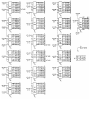
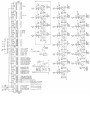
Figure 27-A: Auxiliary PCB Schematic Diagram (2 pages)
Click thumbnails for full-sized versions.
Figure 27-B: Auxiliary PCB Assembly Diagram
Click thumbnail for full-sized version.
Item
1
2
3
4
5
6
7
8
9
10
11
12
13
14
Part Number
006408-01
10-5122
10-5152
10-5183
10-52P7
10-5331
10-5333
10-5683
10-5822
11-5220
12-5153
13-5390
16-5752
10-5204
Figure 27-C: Auxiliary PCB Assembly Parts List
Qty.
Description
1
PCB, Blank, Auxiliary Board
1
Res. CC, 1.2K ohms, 1/4w, 5%
1
Res. CC, 1.5K ohms, 1/4w, 5%
2
Res. CC, 18K ohms, 1/4w, 5%
1
Res. CC, 2.7 ohms, 1/4w, 5%
3
Res. CC, 330 ohms, 1/4w, 5%
3
Res. CC, 33K ohms, 1/4w, 5%
4
Res. CC, 68K ohms, 1/4w, 5%
11 Res. CC, 8.2K ohms, 1/4w, 5%
2
Res. CC, 22 ohms, 1/2w, 5%
2
Res. CC, 15K ohms, 1w, 5%
4
Res. CC, 39 ohms, 2w, 5%
2
Resistor, w.w. , 7.5K ohms, 5w, 5%
1
Res. CC, 200K, 1/4w, 5%
R15
R14
R2, 18
R10
R26, 27, 39
R5, 12, 17
R3, 16, 30, 31
R4, 6-9, 13, 19, 42-45
R28, 29
R24, 25
R40, 41, 46, 47
R37, R38
R48
15
16
17
18
19
20
21
22
23
24
25
26
27
28
29
30
31
32
33
34
35
36
37
38
39
40
41
42
43
44
45
46
47
48
49
50
51
52
53
54
55
56
57
58
59
60
61
62
63
64
65
66
19-311502
24-151506
24-250106
24-250478
24-250477
24-250105
27-250104
27-250103
28-101101
3A-MDA100A
31-1N914
31-1N4005
32-P6KE30
32-1N5235
32-1N5242B
32-1N4763A
33-2N3644
33-2N5883
34-2N3643
34-2N3583
34-2N6044
34-2N6282
33-2N6420
37-LM380
37-MC1413
37-741
37-4016
37-7402
37-7407
1
2
1
1
1
1
9
2
1
1
1
8
1
2
1
2
1
4
2
1
2
1
1
1
1
1
1
2
2
Trimpot, 5000 ohms
Capacitor, Electrolytic,150WVDC, 50ufd
Capacitor, Electrolytic, 25WVDC, 10ufd
Capacitor, Electrolytic, 25WVDC, 4700ufd
Capacitor, Electrolytic, 25WVDC, 470ufd
Capacitor, Electrolytic, 25WVDC, 1.Oufd
Capacitor, Ceramic, 25V, 0.1ufd
Capacitor, Ceramic, 25V, .O1ufd
Capacitor, Mica, 100V, 100pfd
Rectifier Assembly, Bridge, MDA100A
Diode, 1N914
Rectifier, 1N4005
Transient Suppressor Diode, P6KE30
Diode, Zener, 1N5235
Diode, Zener, 1N5242B
Diode, Zener, 1N4763A
Transistor, PNP, 2N3644
Transistor, PNP, 2N5883
Transistor, NPN, 2N3643
Transistor, NPN, 2N3583
Transistor, NPN, 2N6044
Transistor, NPN, 2N6282
Transistor, PNP, 2N6420
Integrated Circuit, LM380
Integrated Circuit, MC1413(ULN2003)
Integrated Circuit, 741
Integrated Circuit, 4016
Integrated Circuit, 7402
Integrated Circuit, 7407
R1
C3, C4
C5
C1
C2
C6
C7, 9-14, 18, 19
C15, C16
C8
nbsp;
CR20
CR10-12, 15-18, 22
CR5
CR3, CR4
CR19
CR13, CR14
Q2
Q6-Q9
Q1, Q12
Q3
Q10, Q11
Q5
Q4
D1
A1
C1
D2
A2, A3
D3, C2
11-5391
72-16O8C
75-016S
75-056
75-916C
12-5103
78-06002
79-58123
79-58124
78-06012
32-1N6335
32-1N5230
10-5101
1
10
10
10
10
1
2
1
1
1
1
1
1
Resistor, Carbon Comp., 390 ohms, 1/2w, 51%
Screw, Mach., Pan Hd- Phillips, 6-32 x 1/2" Lg.
Washer, Flat, Regular Pattern, #6
Washer, Lock, Internal Tooth, #6
Nut, Hex, Regular Pattern, 6-32, Steel
Resistor, Carbon Comp., 10K ohm, 1w, 5%
Heatsink, Therma1loy #6111B-66
Header, 6-pin, Amp #350431-1
Header, 4-pin, Amp #350761-4
Heatsink, Modified Wakefield #641
Diode, Zener, 1N5335
Diode, Zener, 1N5230
Resistor, Carbon Comp., 100 ohms, 1/4w, 5%
R35
78-16011
72-1408C
75-014S
75-054
75-914C
75-09012
78-OA01
2
4
4
4
4
4
2
Silpad, TO-66
Screw, Mach, Pan Hd Phil., #4-40 x 1/2 Cres
Washer, Flat, Reg Pattern #4
Washer, Lock, Int. Tooth #4
Nut, Hex, Reg Pattern #4-40 Cres
Washer, Shoulder
Cover, Insulating, to-66
R36
CR1
CR21
R11
Q10, 11
67
68
69
10-5221
75-09015
10-5201
1
3
2
Res., C.C. 220 Ohms, 1/4w, 5%
Shoulder Washer (Seastrom 5605-25)
Res., C.C., 200 Ohms, 1/2w 5%
R33
R21, 22
Figure 27-C: Auxiliary PCB Assembly Parts List
On the schematic the symbol P (which appears at various inputs to logic gates and other integrated circuits) indicates a connection to +5 volts
through a pull-up resistor.
As an aid for locating integrated circuit devices referred to in the schematics and assembly drawings, and on the boards themselves, each IC
position is given a letter/number designation. On the PCB the IC devices are arranged in columns (along the short dimension of the board) and
rows (along the long dimension). The letter refers to a column, and the number refers to a row.
Thus, for example, the type-9321 IC device given the designation D1 and drawn near the center of sheet 1 is found as the second device in the
"D" row of devices mounted on that board.
Microprocessing unit
The large block drawn along the left side of sheet 1 of the schematic represents the Microprocessing Unit. The signal names for the various
Data Bus, Address Bus and Processor Controls are labeled inside the block.
Program Memory
Eight ROM devices in locations E1 through E8 for the -08 PCB and two ROM devices in locations E00 and E0 for the -09 PCB form the
program memory. Note that the address inputs of all ROMs are connected in parallel and are tied to the A0B through A9B signals. These
signals are produced by buffer logic connected to the Microprocessing Unit's Address Bus (signals AO through A9). Also note that all CE2
inputs (pin 10) are tied together and driven by a common signal, and that the CE1 inputs are driven by signals derived from A10 and A11
produced by the Microprocessing Unit. All ROM data terminals are connected in parallel to the Data Bus (DO through D7).
Although all eight devices are ROMs, they should never be interchanged (that is, E1 unplugged and plugged into the E2 position, and vice
versa), because different data has been programmed in each ROM.
Inside each ROM the data is organized in a 1K x 4 format (1024 bits by 4), giving each ROM a capacity of 4096 data bits.
Data Memory
The four devices in locations D5 through D8 form the Data Memory. Note that all address inputs are connected in parallel (together with the
ROMs) to the A0B through A9B signals, and that all RAM data terminals are connected in parallel (together with the ROMs) to the Data Bus.
The Microprocessing Unit's R/W bus control signal is buffered and then connected to all RAM R/W inputs.
Memory Output Latches
The eight type-9334 devices along the right side of the sheet form the Memory Output Latches. The addressing signals applied to each latch
(at pins 1, 2, and 3) are derived from the A2, A3, and A7 Address Bus signals. One Data Bus bit is applied to each latch device (for example,
Bit DO is applied to the latch in location C20, Bit D1 to C19, and so forth). The ^REG LD^ (Register Load) signal, produced by the Control
Logic, is applied to the ^E^ (Enable not) input of every latch device (at pin 14).
Editor's note: ^THIS^ notation will be used to indicate a horizonal line over words; this is impossible to show in HTML.
Each latch device has eight outputs, giving a total of 64 LATCH signals. Twelve of these (the signals LATCH 1080 BIT 0 through 4, LATCH
1084 BIT 0 through 4, and Latch 1084 BIT 0 through 4), provide the Sound Data, 32 provide the Lamp Data, and the remaining 20 provide
the Solenoid Data.
Clock Generator
The circuit is shown along the bottom of the sheet. The basic frequency source is a 4-MHz crystal-controlled oscillator. Its output is then
shaped, divided down, and buffered to produce the ^(PHI)1^ and ^(PHI)2^ signals (phase 1 not and phase 2 not). These are the
non-overlapping, non-symmetrical square wave complements required by the Microprocessing Unit. They are also used in the Control Logic.
Tri-State Buffers
The two type-8097 devices in locations C4 and C5 on sheet 2 connect Switch Data, power line phasing information, display address
information, and other Control Logic signals to bits D6 and D7 of the Data Bus, and to Bits A0 through A5 and A12 through A14 of the
Address Bus. Keep in mind that these are Tri-State devices. When its control line is in the disable state, a tri-state device's data connections
become a high impedance, the equivalent of removing the device from the circuit. But when the control line is in the enable state, the device's
data connections are capable of having normal high and low ("1" and "0") levels.
Control Logic
The portion of the Control Logic that produces the ^RESET^ signal for the Microprocessing Unit is shown at the top of sheet 2. The five
type-7493 Counter devices form a single, simple binary counter configuration that is driven by the phase 1 clock signal. The AUDIO CLOCK
signal produced by the first 7493 device (at A6 pin 8) is used in the Sound Generator circuit.
If, at any time after power is applied to the game, the count advances far enough to bring the last stage high (A10 pin 9 high), then the
^RESET^ signal will be brought low. (^RESET^ can also be brought low by manually depressing the ^RESET^ pushbutton mounted on
the surface of the Processor PCB.) ^RESET^ going low causes the Microprocessing Unit to begin the restart sequence. The execution of a
routine to initialize the processor from its reset condition will be started.
In normal game operation the ^RESET^ signal stays low. The WAKE-UP RESET signal (applied at pins 2 and 3 of both A9 and A10)
periodically goes high, preventing the last counter stages from going high. If some abnormal circumstance occurs, such as a momentary
interruption in game power caused by severe transients on the AC power line, then the program sequence inside the Microprocessing Unit
may be disrupted and the WAKE-UP RESET signal may remain low for longer than 100 milliseconds. In such a case, a high-to-low-level
transition (positive-going edge) on the ^RESET^ signal is produced, and the microcomputer system resets itself.
Other portions of the Control Logic are covered under the Circuit Descriptions that follow.
C. CIRCUIT DESCRIPTIONS
Solenold Driver Circuits
Twenty of the outputs from the Memory Output Latches constitute the Solenoid Data shown in Figure 23. These are the signals LATC 1080
BIT 4 through 7, LATCH 1084 BIT 4 through 7, LATCH 1088 BIT 4 through 7, and LATCH 108C BIT 0 through 7 (shown on sheet 1 of
Processor PCB schematic).
Two of these signals, LATCH 1080 BIT 4 and 5, connect to the Auxiliary PCB where they each drive a type-7407 Inverter followed by a
2N6044 Darlington- connected transistor pair. The remaining eighteen LATCH signals connect to the same types of devices (7404 and
2N6044) on the Processor PCB.
Figure 30 shows a simplified diagram of the basic solenoid drive circuit for all solenoids. One side of the solenoid coils connects to the
collectors of the 2N6044 transistors; the other side is brought, together with all the other coils, to an unregulated, full-wave rectified DC
power supply of about 35 volts amplitude. This power supply is located in the Power Supply Assembly in the right rear corner of the cabinet.
Note that a suppression diode is placed across each coil; the diode protects the 2N6044 from reverse inductive kickback (back emf) when the
coil is de-energized. The emitters of all 2N6044 devices and the ground side of the 35-volt supply are returned to SOLENOID GRD (at J9, pin
3).
Figure 30: Simplified Diagram of Basic Solenoid Driver Circuit
Remember that the microcomputer, by means of the PHASE signal, is able to synchronize the turning on of the solenoids so that it will start
only at a zero crossing point (zero power point) of the power line waveform.
Drive components for the coin counter metering function are on the Processor PCB. Also provided are signals from the microcomputer and
spaces on the board for additional drive components, so that operators wishing to have four additional functions can do so by installing
additional components. The four functions, components required, and their circuit designations are listed in Table 15. Figure 31 shows the
circuit for each metering function to be added.
Table 15: Components Required for Special Metering Functions
(Available at edge connector J-8 on the main processor PCB)
Processor PCB
2N6044
1N914
Function Being Metered
Edge Connector J8 Pin Driver Number Designation
Total replays
X, 20
10
CR20
Total specials awarded
U, 17
19
CR17
Total game time (min.) V, 18
9
CR18
Total plays
W, 19
20
CR19
Resistor
Designation
R25
R21
R24
R23
Figure 31: Additional Components to be Installed for Each Metering Function Added
Lamp Driver Circuits
Thirty-two of the outputs from the Memory Output Latches constitute the lamp data shown in Figure 23. These are the BIT 0 through BIT 7
signals LATCH 1000, LATCH 1004, LATCH 1008 and LATCH 100C. All thirty-two signals connect to the inputs of the type ULN-2003A
devices shown on sheet 4 of the Processor PCB schematic. These are open-collector interface devices that accept TTL input levels, and
produce the high current outputs needed to light the lamps. Note that these devices connect to a lamp ground (J19, pin 3).
Figure 32 shows a simplified diagram of the basic lamp driver circuit. One side of each lamp connects to a ULN-2003A output terminal, and
the other side connects to a strobe line on the Auxiliary PCB (STROBE A, STROBE B, etc.). In the wiring harness, beneath the playfield,
black wires are used for lamps connecting to STROBE A, green wires for those to STROBE B, blue wires for STROBE C, and red wires for
STROBE D.
Figure 32: Simplified Diagram of Basic Lamp Driver Circuit
The control logic decodes the LAMP BIT 0 and LAMP BIT 1 signals to produce four transistor based drive signals, one for each 2N5883.
(LAMP BIT 0 and LAMP BIT 1 come from the same circuit that produces the DISPLAY ADRS 1 and DISPLAY ADRS 2 signals on the
Processor PCB schematic.) The timing of the four signals driving the 2N5883 transistors is such that any one transistor is brought into
conduction only 25% of the time (25% duty cycle), This means that the playfield lamps, which appear to the eye to be of uniform brightness
when lighted, are in reality blinking on and off.
CAUTION: During troubleshooting of the game by service technicians, while operating the game with the cabinet open and power applied,
do not hold down the RESET pushbutton (mounted on the Processor PCB) for long periods of time. Doing this will cause one of the 2N5883
transistors to be brought into conduction 100% of the time. Lamp current is very high in this situation, and can lead to premature burning out
of the lamps.
Switch Sensing Circuit
The switch sensing circuit accepts switch closure information as an input, and produces switch data as an output. This switch data is sent to
the microcomputer system on a single signal line. Figure 33 shows a simplified diagram of the switch sensing circuit.
Figure 33: Simplified Diagram of Switch Sensing Circuit
The normally open (NO contacts) of the various playfield switches and certain cabinet switches are connected together in the playfield harness
wiring, and then a common lead is brought to the Processor PCB at connector J7 (pins 5 & 6). (Refer to sheet 2 of the Processor PCB
schematic.) On the board's artwork, the NO contacts from the Operator Option Switches (along with signals derived from the rest of the
cabinet switches -- COIN 1, COIN 2, START, and SLAM), are also connected electronically to this point. Also, this point is connected to
resistor R27, tied to +5 volts, and to the pin-13 input of the type-7414 Inverter in location C9. The output of this Inverter, C9 pin 12, is the
Switch Data line, which is applied to pin 12 of the type-8097 tri-state buffer in location C5. The device terminal at C5 pin 11 is connected to
bit D7 of the Microprocessing Unit's bidirectional Data Bus.
By means of multiplexing technique, the switch closure information being sent on the switch data line is derived from the timing of addressing
signals being sent out by the Microprocessing Unit over the Address Bus. To determine whether or not a specific switch is closed, the
Microprocessing Unit compares the timing of that switch's address code with the state of the switch data signal being received at that moment
on bit D7 of the data bus.
Figure 34 shows simplified wave form diagrams that illustrate this timing comparison multiplex technique for an imaginary circuit having
only eleven switches.
Figure 34: Simplified Diagram of Switch Censing Circuit Waveforms
In the actual game, anytime that the Microprocessing Unit addresses a specific switch, and that switch is closed at that moment, the SWITCH
COMMON line will be low. The 7414 Inverter changes this to high, and a high goes out on the Data Bus on bit D7. So when the
Microprocessing Unit reads back a high in that location on the data bus, it knows that the specific switch had been closed.
The control logic used for decoding the Microprocessing Unit's addressing information is shown on the left side of sheet 3 of the schematic.
One SWITCH DECODE line is produced for each switch (switch DECODE 200B, SWITCH DECODE 200A, etc.).
Displays and Display Data
The Score Display consists of a glass plate panel that plugs into an edge connector, and a printed circuit board beneath that plugs into a second
connector. The two connectors are hard-wired together. The Credit and Ball/Match displays are both built on a separate PCB.
WARNING: Whenever AC power is applied to the game, voltage potential differences as large as 180 volts are present at the bare terminals
of the glass plate's edge connector, and at various other points on both printed circuit boards.
All three are gas-discharge type displays with the following principle of operation. If a sufficiently high voltage is applied to a gas, a point
will be reached at which the gas ionizes, producing a conduction current and giving off radiation (which can be in the form of visible light).
Fluorescent lamps are common examples of illumination sources that also make use of the gas-discharge phenomenon.
A display segment lights up when +90 volts is applied to the anode at the same time that -90 volts is applied to the cathode, as illustrated by
the waveforms in Figure 35.
Figure 35: Waveforms for Gas Discharge Displays
Although to the human eye a lighted segment seems to be uniformly bright, in actuality the segment is being turned on and off at a rate faster
than the eye can detect, This technique is called segment multiplexing.
The Microcomputer System block diagram in figure 23 shows how the microprocessing unit addresses the RAM Data Memory (via the
Address Bus) and passes data to this memory (via the Bidirectional Data Bus), and how the Control Logic also shares these buses.
The microprocessing unit brings its BA (Bus Available) signal at C1 pin 7 to high when it is off the buses. During game operation the
microprocessing unit periodically writes new display data into the RAM Data Memory and then gives up the buses. Subsequently the Control
Logic takes over the buses, addressing the RAM Data Memory and then reading its display data off the Bidirectional Data Bus. The Control
Logic then produces the four signals DISPLAY DATA 0 through DISPLAY DATA 3. It also produces seven addressing signals DISPLAY
ADRS 0 through DISPLAY ADRS 6, and three control signals ANODE BLANK, ^CATHODE BLANK^ and ^LOAD DISPLAY^.
The addressing signals are used to identify which displays are to accept data at any given moment. The control signals are used to blank the
displays while the microprocessing unit is on the buses, and to strobe in new display data, respectively.
The circuitry for the Control Logic is shown on the right side of sheet 2 of the Processor PCB schematic. The type-74157 2-line to 1-line
multiplexer in location B5 produces four DISPLAY DATA signals from the eight inputs D0B through D7B (These eight signals come from
the type-LS08 buffers B/C8 and C/D8 on sheet 1; the buffers are driven directly from the Data Bus signals D0 through D7.) The seven
DISPLAY ADRS signals are produced by counters B4 and B3 whose outputs also drive the Address Bus through the type-8097 Tri-State
devices C4 and C5. The three display control signals are produced by timing logic driven also by counters B3 and B4 as well as by the ^BA^
signaI from the microprocessing unit, and by the ^RESET-A^ signal from the microcomputer reset circuit.
The circuit for each display consists of an anode drive portion and a cathode drive portion. The anode portions derive timing signals from the
DISPLAY ADRS 0 through DISPLAY ADRS 2 signals and the ANODE BLANK control signal. The cathode portions perform three
functions: storage of data derived from the DISPLAY DATA signals (under control of the ^LOAD DISPLAY^ signal), decoding of this data
into 7- segment format, and keeping the segments turned off part of the time (under control of the ^CATHODE BLANK^ signal).
The +90 volts and -90 volts required by the displays is produced in a regulated power supply circuit built on the Auxiliary PCB. The 170 VAC
input to this circuit comes from the power transformer located in the Power Supply Assembly.
Credit and Match/Ball Display Circuit
Note that the top half of the Match/Credit PCB Schematic describes the cathode circuitry. The bottom half covers the anode circuitry.
The type-14556 device examines the DISPLAY ADRS 5 and DISPLAY ADRS 6 signals to determine when new data is available for these
display digits. The output from the 14566 device is applied to the LE (Latch Enable) input of a type-14511 device. The four signals DISPLAY
DATA 0 through 3 are applied to the inputs of a type-14511 device. This device has a latching capability and also performs segment
decoding.
The 14511 device's segment outputs are applied to a type-584-8 device that performs an interfacing function; it accepts TTL logic level inputs
and produces a 90-volt swing (from 0 volts to -90 volts) at its output. The seven outputs from this device are applied to the cathode terminals
of all display segments. The CATHODE BLANK signal, applied to the B1 input (pin 4 of the 14511 device), will cause all segments to be
blank, regardless of what data is stored, when the multiplex timing calls for that digit to remain unlighted.
The Type-14028 device, in the anode portion of the circuit, examines the three signals DISPLAY ADRS 0 through 2 to determine which of
the display digits to turn on. The outputs from the 14028 are applied through series-connected diodes to a type-585-6 interface device that
drives the anode terminals of the display digits with a voltage swing from 0 volts to +90 volts.
Figure 29-A: Match/Credit PCB Schematic Diagram
Figure 29-B: Match/Credit PCB Assembly Drawing
Item
1
2
3
4
5
6
7
8
9
10
11
12
13
14
15
16
17
18
Figure 29-C: Match/Credit PCB Assembly Parts List
Part
Number
Description
006104-01 1
PCB, Blank, Match/Credit Display Board
10-5155
2
Resistor, Carbon Comp., 1.5 Megohms, 1/4w, 5%
10-5394
1
Resistor, Carbon Comp., 390K ohms, 1/4w, 5%
12-5103
1
Resistor, Carbon Comp., 10K ohms, 1w, 5%
24-500105 1
Capacitor, Electrolytic, 50 WVDC, 1.0 ufd
24-101106
32-1N5230
37-MC14028
37-MC14511
37-MC14556
37-584-8
37-585-6
19-008
31-1N914
79-41001
10-5104
32-1N4744
2
1
1
1
1
1
1
1
4
2
1
1
Capacitor, Electrolytic, 100 WVDC, 10 ufd
Diode, Zener, 1N5230
Integrated Circuit, MC14028
Integrated Circuit, MC14511
Integrated Circuit, MC14556
Integrated Circuit, 584-8
Integrated Circuit, 585-6
Resistor Network, 10K ohms, CTS#761-1-R10K
Diode, 1N914
Socket, Beckman Type CS-352
Res, Carbon Comp., 100K, 1/4W, 5%
Diode, Zener 1N4744
Figure 29-C: Match/Credit PCB Assembly Parts List
R3, 4
R2
R1
C3
C1, 2
CR1
CR2-5
R5
CR6
Score Display Circuit
The connections to the score display panel are made in the form of a rectangular matrix, with seven anode connections on one side and 28
cathode connections on the other. Figure 36 illustrates the arrangement of these connections. In the multiplex timing the six vertical rows of
digits, plus the one vertical row of player up indications, are driven one at a a time. All the anodes in the player up indications are brought
together electrically to J21, pins 1 and 2, the ANODE 1 signal, All the anodes for the least significant digits are brought to J21, pins 50 and 5,
the ANODE 2 signal, etc. The sequence of lighting the anodes is: ANODE 2, then 4, then 6, then 3, then 5, then 7, and finally ANODE 1.
Likewise, the cathodes of all segments of the digits in a row are tied together, For example, all the "b" segments in the top row are tied
together and brought to J21, pin 46.
Figure 36: Arrangement of Connections to Score Panel
For the circuit descriptions that follow, refer to the schematic in Figure 28. The four display address signals (DISPLAY ADRS 3 through 6)
are applied to type-14556 devices which produce four outputs. One of these outputs is applied to the LE input (pin 5) of each of the
type-14511 Latch/Segment Decoder devices in locations D2, C3, B3, and A2. The 14556 devices decide which of the Latch/Segment
Decoders are to receive display data (are to be loaded) at any one moment.
Figure 28-A: Score Panel Drive PCB Schematic Diagram
Click thumbnail for full-sized version.
Figure 28-B: Score Panel Drive PCB Assembly Drawing
Click thumbnail for full-sized version.
Item
1
2
3
4
5
6
7
8
9
10
11
12
13
14
15
16
17
18
19
20
Part Number
004922-01
10-5102
10-5224
10-5564
10-5822
11-5153
13-5682
24-101106
24-500105
32-1N4751
32-1N5230
19-008
37-MC14028
37-MC14511
37-MC14556
37-MPQ7091
37-UDN6184A
37-584-8
006123-01
004770-01
Qty.
1
8
2
2
4
1
1
2
1
1
1
1
1
4
1
1
1
4
1
1
Figure 28-C: Score Panel Drive PCB Assembly List
Description
PCB, Blank, Score Panel Drive
Res., Carbon Comp., 1000 ohms, 1/4w, 5%
Res., Carbon Comp , 220K, ohms, 1/4w, 5%
Res., Carbon Comp., 560K ohms, 1/4w, 5%
Res., Carbon Comp., 8200 ohms, 1/4w, 5%
Res., Carbon Comp., 15K ohms, 1/2w, 5%
Res., Carbon Comp., 6800 ohms, 2w, 5%
Capacitor, Electrolytic, 100WVDC. 10ufd
Capacitor, Electrolytic, 50WVDC, 1.0ufd
Diode, Zener, 1N4751
Diode, Zener, 1N5230
Res. Network, 1OK ohms, CTS# 761-1-R10K
Integrated Circuit, MC14028
Integrated Circuit, MC14511
Integrated Circuit, MC 14556
Integrated Circuit, MPQ7091
Integrated Circuit, UDN6184A
Integrated Circuit, 584-8
Integrated Circuit, MC1413, 75V (Atari Custom)
Connector, Score Panel
R5-12
R1, 4
R2, 3
R16-19
R14
R13
C1-2
C3
CR9
CR1
21 72-1408S
4
Screw, Mach., Pan Hd., Phil., 4-40 x 1/2" Lg., Stl
22 10-5104
1
Res., Car Comp., 100K ohms 5%
R15
23 32-1N4744
1
Diode, Zener 1N4744
CR10
24 10-5382
1
Res. Car Comp., 1.8K ohms 1/2w, 5%
R20
25 27-10104
1
Capacitor, Ceramic Disc 0.1uf 100V
C4
NOTE: This is the preferred assembly parts lists for the Score Display PCB, to be used when item 17 is obtainable. If item 17 is unavailable
(only) use the assembly parts list, A004924-02 as an alternate procedure.
Figure 28C: Score Panel Drive PCB Assembly Parts List
The individual segment outputs ("a" through "g") produced by the segment decoders are applied to four type-584-8 Cathode Driver devices in
locations D1, C2, B2, and A1. These Cathode Drivers perform an interfacing function; they accept TTL logic level inputs and they produce a
90-volt swing (from 0 volts to -90 volts) at their outputs. A separate circuit (formed by four 8.2K-ohm resistors, a 4-transistor MPQ 7091
device in location A5, and the 006123-01 device in A4), produces the signals applied to the "Player Up" cathodes (4TH UP 3RD UP, etc.)
The circuitry for driving the anodes of the display is shown on the right half of the sheet. The type-14028 device examines the DISPLAY
ADR 0 through 2 signals to determine which of the seven ANODE lines are to be turned on. The outputs of the 14028 are applied to interface
device or devices that will produce the 90-volt swing (from 0 volts to +90 volts) at their outputs. This PCB is laid out in such a way that two
choices of device type are possible. (A board will be built using only one choice.) The choices are: one type-UDN 6184A device, or two
type-585-9 devices.
Sound Generator and Speaker Driver Circuits
The initial portion of the Sound Generator circuit is built on the Processor PCB. The final portion and the Speaker Driver are built on the
Auxiliary PCB. In the lower left corner of sheet 2 of the Processor PCB schematic, four Memory Output Latch signals (LATCH 1088 Bit 0
through LATCH 1088 Bit 3) are applied to the type-9316 counter in location D13. This counter is driven by the AUDIO CLOCK signal and
serves as a frequency generator. The counter's TC (terminal count) output (at D13 pin 15) is applied to a second counter configuration formed
by two type-7493 counter devices. The AUDIO ENABLE and AUDIO RESET signals (produced by Control Logic section shown on
schematic sheet 1) are applied to the R01 and R02 reset inputs of these counters (pins 2 and 3). These two signals control when the Same's
sound is allowed to come on and when it is kept off.
Five output signals from the 7493 counters, together with four more Memory Output Latch signals (LATCH 1080 BIT 0 through BIT 3), are
applied to the address inputs of the ROM device in location D12. This ROM has been pre-programmed to perform a waveform shaping
function. The ROM outputs, AUDIO 0 through AUDIO 3, are sent to the Auxiliary PCB.
On the Auxiliary PCB schematic these four AUDIO signals are connected to type-7407 open-collector buffers. The buffer outputs connect, via
a "weighted" resistor network, to the pin 3 positive input of the amplifier in location C1. The network is called "weighted" because of the
binary-weighted values of the resistors; 68K ohms is double the value of the 33K-ohms resistor which is double the value of the 18K-ohm
resistor, etc. This weighted resistor-buffer arrangement performs a D-to-A (digital to analog) converter function. Note that other resistors, a
1.5K-ohm to ground and a 1.2K-ohm that connects to +13.6 volts, are also tied into this resistor network.
Four more Memory Output Latch signals (LATCH 1084 BIT 0 through BIT 3) are applied to the Auxiliary PCB. After buffering by type-7407
devices, these signals are applied to the gate inputs (pins 5, 6, 12, and 13) of the type-4016 Quad CMOS Analog Switch in location D2. These
four latch outputs provide the amplitude modulation information portion of the Sound Data. The outputs of the type-4016 Analog Switch
connect, via another "weighted" resistor network, to the negative input (pin 2) of amplifier C1. Thus the 4016 device provides amplitude or
gain control for the amplifier. Amplifier C1 acts as a mixer stage for all the Sound Data, and its output (at C1 pin 6) is applied to the Speaker
Drive circuit.
The LM380 amplifier in location D1 serves as the Speaker Driver. Potentiometer R1 provides the game's first speaker volume adjustment. The
LM380 output at D1 pin 8 connects, via harness wiring, to the second speaker volume potentiometer. This potentiometer is located underneath
the cabinet at the front left corner. The wiper of the potentiometer connects directly to the game speaker.
End of Manual
Up to the table of contents
Back to Chapter 3