1
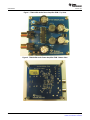
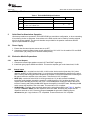
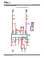
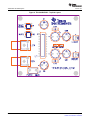
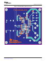
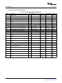
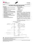
User's Guide
SLOU250 – January 2009
TPA3125D2 EVM
1
2
3
4
Contents
Introduction ...................................................................................................................
Quick Start for Stand-alone Operation ....................................................................................
Schematic and PCB Layers ................................................................................................
Bill of Materials ...............................................................................................................
1
3
5
8
List of Figures
1
2
3
4
5
TPA3125D2
TPA3125D2
TPA3125D2
TPA3125D2
TPA3125D2
Audio Power Amplifier EVM - Top View ...................................................................
Audio Power Amplifier EVM - Bottom View ...............................................................
EVM Schematic...............................................................................................
EVM – Top Side Layout .....................................................................................
EVM – Bottom Side Layout .................................................................................
2
2
5
6
7
List of Tables
1
2
3
TPA3125D2 EVM Specifications .......................................................................................... 3
Gain Jumper Settings ...................................................................................................... 4
TPA3125D2 EVM Bill of Materials ......................................................................................... 8
1
Introduction
1.1
Description
The TPA3125D2 evaluation module (EVM) consists of a single 10-W, class-D, stereo audio power
amplifier, complete with a small number of external components mounted on a printed-circuit board. The
EVM can be used to directly drive speakers with an external analog audio source as the input. Figure 1
and Figure 2 display the top and bottom views of the EVM, respectively. For additional information, consult
the TPA3125D2 data sheet (SLOS611).
SLOU250 – January 2009
Submit Documentation Feedback
TPA3125D2 EVM
1
Introduction
www.ti.com
Figure 1. TPA3125D2 Audio Power Amplifier EVM - Top View
Figure 2. TPA3125D2 Audio Power Amplifier EVM - Bottom View
2
TPA3125D2 EVM
SLOU250 – January 2009
Submit Documentation Feedback
Quick Start for Stand-alone Operation
www.ti.com
1.2
EVM Specifications
Table 1. TPA3125D2 EVM Specifications
Value
2
VCC
Supply voltage range
ICC
Supply current
PO
Continuous output power per channel
8 Ω, VCC = 24V, THD+N=10%
RL
Minimum load impedance
Units
10 to 26
V
3
A
10
W
4
Ω
Quick Start for Stand-alone Operation
Use these procedures to operate the TPA3125D2 EVM in a stand-alone configuration, or when connecting
it into existing circuits or equipment. Connections to the EVM module can be made by inserting stripped
wire for the power supplies. Two pin male headers are provided for the speaker connections and the
inputs accept standard RCA plugs.
2.1
Power Supply
1. Ensure that all external power sources are set to OFF.
2. Connect an external regulated power supply adjusted from 10 V to 26 V to the module VCC and GND
terminal block (J1), taking care to observe marked polarity.
2.2
Evaluation Module Preparations
2.2.1
Inputs and Outputs
1. Connect the left and right speakers across LOUT and ROUT respectively.
2. Install both gain jumpers GAIN0 and GAIN1. This sets the amplifier gain to the lowest level, 20 dB.
2.2.2
Control Inputs
SHUTDOWN (S1) —terminal is active LOW. A LOW on the device terminal (less than 0.8 V) shuts
down the amplifier; a HIGH (greater than 2 V) on the device terminal places the amplifier in the active
state. Pressing and holding the switch S1 places the amplifier in the SHUTDOWN state. Releasing the
S1 switch returns the amplifier to the active state. This terminal is VCC compliant.
• MUTE (S2)—terminal is active HIGH. A HIGH (greater than 2 V) on this terminal immediately
terminates audio playback through the speakers; a LOW (less than 0.8 V) enables the device. The
outputs remain switching with a 50% duty cycle. The EVM S2 switch controls the state of the MUTE
terminal. Pressing and holding the S2 switch places the amplifier in the MUTE state. Releasing the S2
switch returns the amplifier to the active state. This terminal is VCC compliant.
• GAIN0/GAIN1—Together, these terminals determine the gain of the amplifier (see Table 2). Installing
a jumper in GAIN0 or GAIN1 sets the respective terminal to GND. Removing the jumper sets the
respective terminals to VCC. Removing jumpers increases the gain while installing jumpers
decreases the gain. Logic levels are TTL compatible. These terminals are VCC compliant.
•
SLOU250 – January 2009
Submit Documentation Feedback
TPA3125D2 EVM
3
Quick Start for Stand-alone Operation
www.ti.com
Table 2. Gain Jumper Settings
GAIN1
GAIN0
ON
ON
20
ON
OFF
26
OFF
ON
32
OFF
OFF
36
(1)
2.2.3
1.
2.
3.
4.
4
(1)
Amplifier Gain (dB)
OFF denotes jumper is REMOVED; ON denotes jumper
INSTALLED.
Applying Power to the EVM
Verify correct voltage and input polarity for the external power supplies. Turn ON. The EVM starts
operation.
Adjust the input signal.
Adjust the control inputs to the desired settings as described in the Control Inputs section.
Adjust the amplifier gain by installing or removing the gain jumpers, GAIN0 and GAIN1 to yield the
gain values described in Table 2.
TPA3125D2 EVM
SLOU250 – January 2009
Submit Documentation Feedback
SLOU250 – January 2009
Submit Documentation Feedback
2
1
GND
RCA (Red)
RCA (Black)
GRAY
6A/250V
J1
PVCC
1
3
2
1
3
2
C6
GND
1.0ufd/16V
GND
1.0ufd/16V
C5
FB2
1000pfd/50V
0603
C3
GND
GND
1000pfd/50V
0603
GND
C11
1.0ufd/50V
0805
1.0ufd/16V
0603
C8
C10
GND
GND
1.0ufd/16V
0603
C7
10K
0603
R2
GND
1.0ufd/16V
0603
C4
GND
GND
PVCCR
10K
0603
R1
1.0ufd/50V
0805
C2
GND
PVCC
2
1
80ohms/100MHz
0805
S2
470ufd/35V
HE
C9
GND
+
PVCC
0603
0603
PVCC
GND
S1
470ufd/35V
HE
C1
GND
+
FB1
2
1
80ohms/100MHz
0805
10
9
8
7
6
5
4
3
2
1
GND
2
HS1
1
TPA3125D2N
U1
C15
GND
0.22ufd/25V
FB4
GND
GND
1
2
1
2
2mm
2mm
GAIN1
GAIN0
PVCCR
GND
GND
GND
GND
0.875in 0.875in 0.875in 0.875in
STANDOFFS
2
1
80ohms/100MHz
0805
10K
0603
10K
0603
0603
R4
R3
GND
0.0
1210
GND
C14
R9
10ufd/50V
1210
0603
FB3
2
1
80ohms/100MHz
0805
1000pfd/50V
0603
C13
0.22ufd/25V
C12
GND
2W@60C
11
12
13
14
15
16
17
18
19
20
GAIN0
GAIN1
SHUNTS
GND
1500pfd/50V
0603
C17
10,1/4W
1206
R6
GND
1500pfd/50V
0603
C16
10,1/4W
1206
R5
L1
33uH/2.3A
L2
33uH/2.3A
GND
0.22ufd/63V
MKT
C19
GND
0.22ufd/63V
MKT
C18
GND
1.00K
0603
R8
GND
1.00K
0603
R7
C20
C21
470ufd/35V
HE
+
470ufd/35V
HE
GND
GND
1
2
1
2
ROUT
LOUT
3
+
PVCC
www.ti.com
Schematic and PCB Layers
Schematic and PCB Layers
Figure 3. TPA3125D2 EVM Schematic
TPA3125D2 EVM
5
Schematic and PCB Layers
www.ti.com
Figure 4. TPA3125D2 EVM – Top Side Layout
6
TPA3125D2 EVM
SLOU250 – January 2009
Submit Documentation Feedback
Schematic and PCB Layers
www.ti.com
Figure 5. TPA3125D2 EVM – Bottom Side Layout
SLOU250 – January 2009
Submit Documentation Feedback
TPA3125D2 EVM
7
Bill of Materials
4
www.ti.com
Bill of Materials
All components should be lead-free.
Table 3. TPA3125D2 EVM Bill of Materials
RefDes
Description
Qty
Mfr Part No.
Mfr
Vendor Part No.
Vendor
U1
10W STEREO CLASS-D AUDIO POWER AMP
N20-DIP ROHS
1
TPA3125D2N
Texas
Instruments
TPA3125D2N
Texas
Instruments
C3, C11, C13
CAP 1000PFD 50V 5% CERM 0603 COG ROHS
3
C1608C0G1H102J
TDK Corp.
445-1293-1
Digi-Key
C16, C17
CAP SMD0603 CERM 1500pfd 50V 10% X7R ROHS
2
C0603C152K5RACTU
Kemet
399-1084-1
Digi-Key
C12, C15
CAP SMT0603 CERM 0.22µF, 25V 10% X5R ROHS
2
06033D224KAT2A
AVX
478-1245-1
Digi-Key
C18, C19
METAL POLY CAP THU MKT 0.22µF, 63V 10%
ROHS
2
B32559C224K000
EPCOS
495-2814
Digi-Key
C4–C8
CAP SMT0603 CERM 1.0µF, 16V 10% X5R ROHS
5
ECJ-1VB1C105K
Panasonic
PCC2224CT
Digi-Key
C2, C10
CAP SMT0805 CERM 1.0µF, 50V 10% X7R ROHS
2
GRM21BR71H105KA12L Murata
490-4736-1
Digi-Key
C14
CAP SMD1210 CERM 10µF, 50V Y5V ROHS
1
ECJ-4YF1H106Z
Panasonic
PCC2308CT
Digi-Key
C1, C9, C20,
C21
CAP 470UFD 35V RAD ALUM ELEC HE ROHS
4
UHE1V471MHD6
Nichicon
493-1583
Digi-Key
R7, R8
RES 1.00K OHM 1/10W 1% SMD 0603 ROHS
2
RC0603FR-071KL
Yageo
311-1.00KHRCT
Digi-Key
R9
RESISTOR SMD1210 0.0 Ω 1/3W ROHS
1
CRCW12100000Z0EA
Vishay
541-0.0VCT
Digi-Key
R1–R4
RES SMT0603 10K 5% 1/10W ROHS
4
ERJ-3GEYJ103V
Panasonic
P10KGCT
Digi-Key
R5, R6
RESISTOR SMT1206 10.0Ω 1% 1/4W ROHS
2
ERJ-8ENF10R0
Panasonic
P10.0FCT
Digi-Key
L1, L2
INDUCTOR SERIES 11RHBP/A7503AY 33µH/2.3A
ROHS
2
A7503AY-330M
TOKO
A7503AY-330M
TOKO
FB1–FB4
FERRITE BEAD SMD0805 80 Ω at 100MHz 5A
ROHS
4
HI0805R800R-10
Steward
240-2395-1
Digi-Key
GAIN0,
GAIN1
HEADER 2 PIN, PCB 2.0MM ROHS
2
26630201RP2
Norcomp
2663S-02
Digi-Key
LOUT, ROUT
HEADER MALE 2PIN 100LS W/ FRICTION LOCK
ROHS
2
22-23-2021
Molex
WM4200
Digi-Key
RIN
JACK, RCA 3-PIN PCB-RA RED ROHS
1
PJRAN1X1U03X
Switchcraft
89K7617
Newark
LIN
JACK, RCA 3-PIN PCB-RA BLACK ROHS
1
PJRAN1X1U01X
Switchcraft
65K7770
Newark
J1
TERMINAL BLOCK 2PIN 6A/250V GRAY 7mm
PITCH 16-28AWG ROHS
1
ED655/2DS
On Shore
Technology
ED1534
Digi-Key
S1, S2
SWITCH MOM TACT 100GF TH 4PIN 6×6MM ROHS
2
FSMCDH
TycoAlcoswitch
450-1654
Digi-Key
GAIN0,
GAIN1
SHUNT, BLACK AU FLASH 2mmLS
2
810-002-SP2L001
Norcomp Inc.
SP2-001E
Digi-Key
HS1
HEATSINK DIP20 BLACK 2W ROHS
1
580400B00000G
AAVID
Thermalloy
580400B00000G
AAVID
Thermalloy
SO1–S04
4-40 SCREW, STEEL 0.250 IN
4
PMS 440 0025 PH
Building
Fasteners
H342
Digi-Key
SO1–S04
STANDOFF, 4-40, 0.875IN×3/16IN, ALUM RND F-F
4
2030
Keystone
Electronics
2030K
Digi-Key
8
TPA3125D2 EVM
SLOU250 – January 2009
Submit Documentation Feedback
EVALUATION BOARD/KIT IMPORTANT NOTICE
Texas Instruments (TI) provides the enclosed product(s) under the following conditions:
This evaluation board/kit is intended for use for ENGINEERING DEVELOPMENT, DEMONSTRATION, OR EVALUATION PURPOSES
ONLY and is not considered by TI to be a finished end-product fit for general consumer use. Persons handling the product(s) must have
electronics training and observe good engineering practice standards. As such, the goods being provided are not intended to be complete
in terms of required design-, marketing-, and/or manufacturing-related protective considerations, including product safety and environmental
measures typically found in end products that incorporate such semiconductor components or circuit boards. This evaluation board/kit does
not fall within the scope of the European Union directives regarding electromagnetic compatibility, restricted substances (RoHS), recycling
(WEEE), FCC, CE or UL, and therefore may not meet the technical requirements of these directives or other related directives.
Should this evaluation board/kit not meet the specifications indicated in the User’s Guide, the board/kit may be returned within 30 days from
the date of delivery for a full refund. THE FOREGOING WARRANTY IS THE EXCLUSIVE WARRANTY MADE BY SELLER TO BUYER
AND IS IN LIEU OF ALL OTHER WARRANTIES, EXPRESSED, IMPLIED, OR STATUTORY, INCLUDING ANY WARRANTY OF
MERCHANTABILITY OR FITNESS FOR ANY PARTICULAR PURPOSE.
The user assumes all responsibility and liability for proper and safe handling of the goods. Further, the user indemnifies TI from all claims
arising from the handling or use of the goods. Due to the open construction of the product, it is the user’s responsibility to take any and all
appropriate precautions with regard to electrostatic discharge.
EXCEPT TO THE EXTENT OF THE INDEMNITY SET FORTH ABOVE, NEITHER PARTY SHALL BE LIABLE TO THE OTHER FOR ANY
INDIRECT, SPECIAL, INCIDENTAL, OR CONSEQUENTIAL DAMAGES.
TI currently deals with a variety of customers for products, and therefore our arrangement with the user is not exclusive.
TI assumes no liability for applications assistance, customer product design, software performance, or infringement of patents or
services described herein.
Please read the User’s Guide and, specifically, the Warnings and Restrictions notice in the User’s Guide prior to handling the product. This
notice contains important safety information about temperatures and voltages. For additional information on TI’s environmental and/or
safety programs, please contact the TI application engineer or visit www.ti.com/esh.
No license is granted under any patent right or other intellectual property right of TI covering or relating to any machine, process, or
combination in which such TI products or services might be or are used.
FCC Warning
This evaluation board/kit is intended for use for ENGINEERING DEVELOPMENT, DEMONSTRATION, OR EVALUATION PURPOSES
ONLY and is not considered by TI to be a finished end-product fit for general consumer use. It generates, uses, and can radiate radio
frequency energy and has not been tested for compliance with the limits of computing devices pursuant to part 15 of FCC rules, which are
designed to provide reasonable protection against radio frequency interference. Operation of this equipment in other environments may
cause interference with radio communications, in which case the user at his own expense will be required to take whatever measures may
be required to correct this interference.
Mailing Address: Texas Instruments, Post Office Box 655303, Dallas, Texas 75265
Copyright © 2008, Texas Instruments Incorporated
EVM WARNINGS AND RESTRICTIONS
It is important to operate this EVM within the input voltage range of 10 V to 30 V and the output voltage range of 0 V to 30 V.
Exceeding the specified input range may cause unexpected operation and/or irreversible damage to the EVM. If there are questions
concerning the input range, please contact a TI field representative prior to connecting the input power.
Applying loads outside of the specified output range may result in unintended operation and/or possible permanent damage to the EVM.
Please consult the EVM User's Guide prior to connecting any load to the EVM output. If there is uncertainty as to the load specification,
please contact a TI field representative.
During normal operation, some circuit components may have case temperatures greater than 85°C. The EVM is designed to operate
properly with certain components above 85°C as long as the input and output ranges are maintained. These components include but are
not limited to linear regulators, switching transistors, pass transistors, and current sense resistors. These types of devices can be identified
using the EVM schematic located in the EVM User's Guide. When placing measurement probes near these devices during operation,
please be aware that these devices may be very warm to the touch.
Mailing Address: Texas Instruments, Post Office Box 655303, Dallas, Texas 75265
Copyright © 2009, Texas Instruments Incorporated
IMPORTANT NOTICE
Texas Instruments Incorporated and its subsidiaries (TI) reserve the right to make corrections, modifications, enhancements, improvements,
and other changes to its products and services at any time and to discontinue any product or service without notice. Customers should
obtain the latest relevant information before placing orders and should verify that such information is current and complete. All products are
sold subject to TI’s terms and conditions of sale supplied at the time of order acknowledgment.
TI warrants performance of its hardware products to the specifications applicable at the time of sale in accordance with TI’s standard
warranty. Testing and other quality control techniques are used to the extent TI deems necessary to support this warranty. Except where
mandated by government requirements, testing of all parameters of each product is not necessarily performed.
TI assumes no liability for applications assistance or customer product design. Customers are responsible for their products and
applications using TI components. To minimize the risks associated with customer products and applications, customers should provide
adequate design and operating safeguards.
TI does not warrant or represent that any license, either express or implied, is granted under any TI patent right, copyright, mask work right,
or other TI intellectual property right relating to any combination, machine, or process in which TI products or services are used. Information
published by TI regarding third-party products or services does not constitute a license from TI to use such products or services or a
warranty or endorsement thereof. Use of such information may require a license from a third party under the patents or other intellectual
property of the third party, or a license from TI under the patents or other intellectual property of TI.
Reproduction of TI information in TI data books or data sheets is permissible only if reproduction is without alteration and is accompanied
by all associated warranties, conditions, limitations, and notices. Reproduction of this information with alteration is an unfair and deceptive
business practice. TI is not responsible or liable for such altered documentation. Information of third parties may be subject to additional
restrictions.
Resale of TI products or services with statements different from or beyond the parameters stated by TI for that product or service voids all
express and any implied warranties for the associated TI product or service and is an unfair and deceptive business practice. TI is not
responsible or liable for any such statements.
TI products are not authorized for use in safety-critical applications (such as life support) where a failure of the TI product would reasonably
be expected to cause severe personal injury or death, unless officers of the parties have executed an agreement specifically governing
such use. Buyers represent that they have all necessary expertise in the safety and regulatory ramifications of their applications, and
acknowledge and agree that they are solely responsible for all legal, regulatory and safety-related requirements concerning their products
and any use of TI products in such safety-critical applications, notwithstanding any applications-related information or support that may be
provided by TI. Further, Buyers must fully indemnify TI and its representatives against any damages arising out of the use of TI products in
such safety-critical applications.
TI products are neither designed nor intended for use in military/aerospace applications or environments unless the TI products are
specifically designated by TI as military-grade or "enhanced plastic." Only products designated by TI as military-grade meet military
specifications. Buyers acknowledge and agree that any such use of TI products which TI has not designated as military-grade is solely at
the Buyer's risk, and that they are solely responsible for compliance with all legal and regulatory requirements in connection with such use.
TI products are neither designed nor intended for use in automotive applications or environments unless the specific TI products are
designated by TI as compliant with ISO/TS 16949 requirements. Buyers acknowledge and agree that, if they use any non-designated
products in automotive applications, TI will not be responsible for any failure to meet such requirements.
Following are URLs where you can obtain information on other Texas Instruments products and application solutions:
Products
Amplifiers
Data Converters
DLP® Products
DSP
Clocks and Timers
Interface
Logic
Power Mgmt
Microcontrollers
RFID
RF/IF and ZigBee® Solutions
amplifier.ti.com
dataconverter.ti.com
www.dlp.com
dsp.ti.com
www.ti.com/clocks
interface.ti.com
logic.ti.com
power.ti.com
microcontroller.ti.com
www.ti-rfid.com
www.ti.com/lprf
Applications
Audio
Automotive
Broadband
Digital Control
Medical
Military
Optical Networking
Security
Telephony
Video & Imaging
Wireless
www.ti.com/audio
www.ti.com/automotive
www.ti.com/broadband
www.ti.com/digitalcontrol
www.ti.com/medical
www.ti.com/military
www.ti.com/opticalnetwork
www.ti.com/security
www.ti.com/telephony
www.ti.com/video
www.ti.com/wireless
Mailing Address: Texas Instruments, Post Office Box 655303, Dallas, Texas 75265
Copyright © 2009, Texas Instruments Incorporated