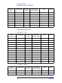
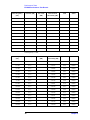
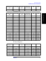
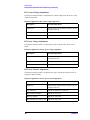
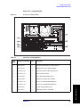
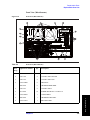
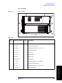
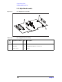
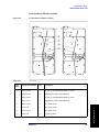
1
Agilent E5052B Signal Source Analyzer
Service Guide
Sixth Edition
Manufacturing No. E5052-90240
October 2012
Notices
The information contained in this document is subject to change without notice.
This document contains proprietary information that is protected by copyright. All rights
are reserved. No part of this document may be photocopied, reproduced, or translated to
another language without the prior written consent of Agilent Technologies.
Microsoft®,MS-DOS®,Windows®,Visual C++®,Visual Basic®,VBA® and Excel® are
registered
UNIX is a registered trademark in U.S. and other countries, licensed
exclusively through X/Open Company Limited.
Portions ©Copyright 1996, Microsoft Corporation. All rights reserved.
© Copyright 2007,2008, 2009, 2012 Agilent Technologies
Manual Printing History
The manual’s printing date and part number indicate its current edition. The printing date
changes when a new edition is printed. (Minor corrections and updates that are
incorporated at reprint do not cause the date to change.) The manual part number changes
when extensive technical changes are incorporated.
May 2007
First Edition
November 2007
Second Edition
December 2008
Third Edition
February 2009
Fourth Edition
April 2009
Fifth Edition
October 2012
Sixth Edition
2
Safety Summary
The following general safety precautions must be observed during all phases of operation,
service, and repair of this instrument. Failure to comply with these precautions or with
specific WARNINGS elsewhere in this manual may impair the protection provided by the
equipment. Such noncompliance would also violate safety standards of design,
manufacture, and intended use of the instrument. Agilent Technologies assumes no liability
for the customer’s failure to comply with these precautions.
NOTE
The E5052B complies with INSTALLATION CATEGORY II as well as POLLUTION
DEGREE 2 in IEC61010-1. The E5052B is an INDOOR USE product.
NOTE
The LEDs in the E5052B are Class 1 in accordance with IEC60825-1,
CLASS 1 LED PRODUCT
NOTE
This equipment is MEASUREMENT CATEGORY I (CAT I). Do not use for CAT II, III, or
IV.
NOTE
This equipment is tested with stand-alone condition or with the combination with the
accessories supplied by Agilent Technologies against the requirement of the standards
described in the Declaration of Conformity. If it is used as a system component,
compliance of related regulations and safety requirements are to be confirmed by the
builder of the system.
•
Ground the Instrument
To avoid electric shock, the instrument chassis and cabinet must be grounded with the
supplied power cable’s grounding prong.
•
DO NOT Operate in an Explosive Atmosphere
Do not operate the instrument in the presence of inflammable gasses or fumes.
Operation of any electrical instrument in such an environment clearly constitutes a
safety hazard.
•
Keep Away from Live Circuits
Operators must not remove instrument covers. Component replacement and internal
adjustments must be made by qualified maintenance personnel. Do not replace
components with the power cable connected. Under certain conditions, dangerous
voltage levels may remain even after the power cable has been disconnected. To avoid
injuries, always disconnect the power and discharge circuits before touching them.
•
DO NOT Service or Adjust the Instrument Alone
Do not attempt internal service or adjustment unless another person, capable of
rendering first aid and resuscitation, is present.
•
DO NOT Substitute Parts or Modify the Instrument
To avoid the danger of introducing additional hazards, do not install substitute parts or
perform unauthorized modifications to the instrument. Return the instrument to an
3
Agilent Technologies Sales and Service Office for service and repair to ensure that
safety features are maintained in operational condition.
•
Dangerous Procedure Warnings
Warnings, such as the example below, precede potentially dangerous procedures
throughout this manual. Instructions contained in the warnings must be followed.
WARNING
Dangerous voltage levels, capable of causing death, are present in this instrument.
Use extreme caution when handling, testing, and adjusting this instrument.
•
Do not connect the measuring terminals to mains.
Safety Symbols
General definitions of safety symbols used on the instrument or in manuals are listed
below.
Instruction Manual symbol: the product is marked with this symbol when it is necessary for
the user to refer to the instrument manual.
Alternating current.
Direct current.
On (Supply).
Off (Supply).
In position of push-button switch.
Out position of push-button switch.
Frame (or chassis) terminal. A connection to the frame (chassis) of the equipment which
normally include all exposed metal structure.
Stand-by.
WARNING
This warning sign denotes a hazard. It calls attention to a procedure, practice,
condition or the like, which, if not correctly performed or adhered to, could result in
injury or death to personnel.
CAUTION
This Caution sign denotes a hazard. It calls attention to a procedure, practice, condition or
the like, which, if not correctly performed or adhered to, could result in damage to or
destruction of part or all of the product.
NOTE
Note denotes important information. It calls attention to a procedure, practice, condition or
the like, which is essential to highlight.
4
Certification
Agilent Technologies certifies that this product met its published specifications at the time
of shipment from the factory. Agilent Technologies further certifies that its calibration
measurements are traceable to the United States National Institute of Standards and
Technology, to the extent allowed by the Institution’s calibration facility, or to the
calibration facilities of other International Standards Organization members.
Documentation Warranty
The material contained in this document is provided "as is," and is subject to being
changed, without notice, in future editions. Further, to the maximum extent permitted by
applicable law, Agilent disclaims all warranties, either express or implied with regard to
this manual and any information contained herein, including but not limited to the implied
warranties of merchantability and fitness for a particular purpose. Agilent shall not be
liable for errors or for incidental or consequential damages in connection with the
furnishing, use, or performance of this document or any information contained herein.
Should Agilent and the user have a separate written agreement with warranty terms
covering the material in this document that conflict with these terms, the warranty terms in
the separate agreement will control.
Exclusive Remedies
The remedies provided herein are buyer’s sole and exclusive remedies. Agilent
Technologies shall not be liable for any direct, indirect, special, incidental, or
consequential damages, whether based on contract, tort, or any other legal theory.
Assistance
Product maintenance agreements and other customer assistance agreements are available
for Agilent Technologies products.
For any assistance, contact your nearest Agilent Technologies Sales and Service Office.
Addresses are provided at the back of this manual.
5
Typeface Conventions
Sample (bold)
Boldface type is used when a term is defined or
emphasised.
Sample (Italic)
Italic type is used for emphasis.
key / [Sample] key
Indicates a hardkey (key on the front panel or
external keyboard) labeled “Sample.” “key” may
be omitted.
Sample menu/button/box
Indicates a menu/button/box on the screen labeled
“Sample” which can be selected/executed by
clicking. “menu,” “button,” or “box” may be
omitted.
Sample block/toolbar
Indicates a block (group of hardkeys) or a toolbar
(setup toolbar) labeled “Sample.”
Sample 1 - Sample 2 - Sample 3
Indicates a sequential operation of Sample 1,
Sample 2, and Sample 3 (menu, button, or box).
“-” may be omitted.
6
Contents
1. General Information
Precautions . . . . . . . . . . . . . . . . . . . . . . . . . . . . . . . . . . . . . . . . . . . . . . . . . . . . . . . . . . . . . . . . . . . . . . . . . . 10
Software Installed . . . . . . . . . . . . . . . . . . . . . . . . . . . . . . . . . . . . . . . . . . . . . . . . . . . . . . . . . . . . . . . . . . . 10
Organization of Service Guide . . . . . . . . . . . . . . . . . . . . . . . . . . . . . . . . . . . . . . . . . . . . . . . . . . . . . . . . . . . 11
Instrument Covered by This Manual . . . . . . . . . . . . . . . . . . . . . . . . . . . . . . . . . . . . . . . . . . . . . . . . . . . . . . 13
Required Equipment . . . . . . . . . . . . . . . . . . . . . . . . . . . . . . . . . . . . . . . . . . . . . . . . . . . . . . . . . . . . . . . . . . . 14
2.
Performance Tests
Introduction. . . . . . . . . . . . . . . . . . . . . . . . . . . . . . . . . . . . . . . . . . . . . . . . . . . . . . . . . . . . . . . . . . . . . . . . . . 18
Test Equipment Required . . . . . . . . . . . . . . . . . . . . . . . . . . . . . . . . . . . . . . . . . . . . . . . . . . . . . . . . . . . . . 18
Individual Test Description. . . . . . . . . . . . . . . . . . . . . . . . . . . . . . . . . . . . . . . . . . . . . . . . . . . . . . . . . . . . . . 19
1. RF IN Port VSWR Test . . . . . . . . . . . . . . . . . . . . . . . . . . . . . . . . . . . . . . . . . . . . . . . . . . . . . . . . . . . . 19
2. Frequency Measurement Test . . . . . . . . . . . . . . . . . . . . . . . . . . . . . . . . . . . . . . . . . . . . . . . . . . . . . . . . 20
3. Power Measurement Accuracy Test . . . . . . . . . . . . . . . . . . . . . . . . . . . . . . . . . . . . . . . . . . . . . . . . . . . 21
4. Phase Noise Accuracy Test . . . . . . . . . . . . . . . . . . . . . . . . . . . . . . . . . . . . . . . . . . . . . . . . . . . . . . . . . . 22
5. SSB Phase Noise Sensitivity Test . . . . . . . . . . . . . . . . . . . . . . . . . . . . . . . . . . . . . . . . . . . . . . . . . . . . . 23
6. SA Relative Level Accuracy Test . . . . . . . . . . . . . . . . . . . . . . . . . . . . . . . . . . . . . . . . . . . . . . . . . . . . . 24
7. DC Power Voltage Test . . . . . . . . . . . . . . . . . . . . . . . . . . . . . . . . . . . . . . . . . . . . . . . . . . . . . . . . . . . . . 25
8. DC Power Current Measurement Test . . . . . . . . . . . . . . . . . . . . . . . . . . . . . . . . . . . . . . . . . . . . . . . . . 26
E5052B Performance Test Calculation Sheet . . . . . . . . . . . . . . . . . . . . . . . . . . . . . . . . . . . . . . . . . . . . . . . . 27
Introduction . . . . . . . . . . . . . . . . . . . . . . . . . . . . . . . . . . . . . . . . . . . . . . . . . . . . . . . . . . . . . . . . . . . . . . . . 27
Phase Noise Accuracy Test . . . . . . . . . . . . . . . . . . . . . . . . . . . . . . . . . . . . . . . . . . . . . . . . . . . . . . . . . . . . 27
SA Relative Level Accuracy Test . . . . . . . . . . . . . . . . . . . . . . . . . . . . . . . . . . . . . . . . . . . . . . . . . . . . . . . 29
E5052B Performance Test Record . . . . . . . . . . . . . . . . . . . . . . . . . . . . . . . . . . . . . . . . . . . . . . . . . . . . . . . . 32
RF IN Port VSWR Test . . . . . . . . . . . . . . . . . . . . . . . . . . . . . . . . . . . . . . . . . . . . . . . . . . . . . . . . . . . . . . . 32
Frequency Measurement Test . . . . . . . . . . . . . . . . . . . . . . . . . . . . . . . . . . . . . . . . . . . . . . . . . . . . . . . . . . 32
Power Measurement Accuracy Test . . . . . . . . . . . . . . . . . . . . . . . . . . . . . . . . . . . . . . . . . . . . . . . . . . . . . 34
Phase Noise Accuracy Test . . . . . . . . . . . . . . . . . . . . . . . . . . . . . . . . . . . . . . . . . . . . . . . . . . . . . . . . . . . . 36
SSB Phase Noise Sensitivity Test (for Standard) . . . . . . . . . . . . . . . . . . . . . . . . . . . . . . . . . . . . . . . . . . . 37
SSB Phase Noise Sensitivity Test (for Option 011) . . . . . . . . . . . . . . . . . . . . . . . . . . . . . . . . . . . . . . . . . 37
SA Relative Level Accuracy Test . . . . . . . . . . . . . . . . . . . . . . . . . . . . . . . . . . . . . . . . . . . . . . . . . . . . . . . 37
DC Power Voltage Test . . . . . . . . . . . . . . . . . . . . . . . . . . . . . . . . . . . . . . . . . . . . . . . . . . . . . . . . . . . . . . . 39
DC Current Measurement Test . . . . . . . . . . . . . . . . . . . . . . . . . . . . . . . . . . . . . . . . . . . . . . . . . . . . . . . . . 40
3. Adjustment
Safety Considerations . . . . . . . . . . . . . . . . . . . . . . . . . . . . . . . . . . . . . . . . . . . . . . . . . . . . . . . . . . . . . . . . . . 42
Warm-up for Adjustment . . . . . . . . . . . . . . . . . . . . . . . . . . . . . . . . . . . . . . . . . . . . . . . . . . . . . . . . . . . . . . . 42
Required Equipment . . . . . . . . . . . . . . . . . . . . . . . . . . . . . . . . . . . . . . . . . . . . . . . . . . . . . . . . . . . . . . . . . . . 42
Required Adjustment after Replacing Assembly . . . . . . . . . . . . . . . . . . . . . . . . . . . . . . . . . . . . . . . . . . . . . 43
Writing ID . . . . . . . . . . . . . . . . . . . . . . . . . . . . . . . . . . . . . . . . . . . . . . . . . . . . . . . . . . . . . . . . . . . . . . . . . 43
DC Control Voltage Adjustment . . . . . . . . . . . . . . . . . . . . . . . . . . . . . . . . . . . . . . . . . . . . . . . . . . . . . . . . 44
DC Power Voltage Adjustment . . . . . . . . . . . . . . . . . . . . . . . . . . . . . . . . . . . . . . . . . . . . . . . . . . . . . . . . . 44
DC Power Current Adjustment . . . . . . . . . . . . . . . . . . . . . . . . . . . . . . . . . . . . . . . . . . . . . . . . . . . . . . . . . 44
Reference Frequency Adjustment . . . . . . . . . . . . . . . . . . . . . . . . . . . . . . . . . . . . . . . . . . . . . . . . . . . . . . . 45
Pre-LO Sampler PLL BW Adjustment . . . . . . . . . . . . . . . . . . . . . . . . . . . . . . . . . . . . . . . . . . . . . . . . . . . 45
Receiver DC offset Adjustment . . . . . . . . . . . . . . . . . . . . . . . . . . . . . . . . . . . . . . . . . . . . . . . . . . . . . . . . 45
PM Offset Adjustment. . . . . . . . . . . . . . . . . . . . . . . . . . . . . . . . . . . . . . . . . . . . . . . . . . . . . . . . . . . . . . . . 46
PM Linearity Adjustment . . . . . . . . . . . . . . . . . . . . . . . . . . . . . . . . . . . . . . . . . . . . . . . . . . . . . . . . . . . . . 47
1
Contents
PM Temp Adjustment . . . . . . . . . . . . . . . . . . . . . . . . . . . . . . . . . . . . . . . . . . . . . . . . . . . . . . . . . . . . . . . .
PM Flatness Adjustment . . . . . . . . . . . . . . . . . . . . . . . . . . . . . . . . . . . . . . . . . . . . . . . . . . . . . . . . . . . . . .
Receiver RF Flatness Adjustment. . . . . . . . . . . . . . . . . . . . . . . . . . . . . . . . . . . . . . . . . . . . . . . . . . . . . . .
Receiver IF Gain/Flatness Adjustment . . . . . . . . . . . . . . . . . . . . . . . . . . . . . . . . . . . . . . . . . . . . . . . . . . .
Receiver RF Flatness Dir Adjustment . . . . . . . . . . . . . . . . . . . . . . . . . . . . . . . . . . . . . . . . . . . . . . . . . . .
Receiver IF Gain/Flatness Dir Adjustment. . . . . . . . . . . . . . . . . . . . . . . . . . . . . . . . . . . . . . . . . . . . . . . .
LO Sampler PLL BW Adjustment . . . . . . . . . . . . . . . . . . . . . . . . . . . . . . . . . . . . . . . . . . . . . . . . . . . . . .
Phase Noise BW Adjustment . . . . . . . . . . . . . . . . . . . . . . . . . . . . . . . . . . . . . . . . . . . . . . . . . . . . . . . . . .
FLL BW Adjustment . . . . . . . . . . . . . . . . . . . . . . . . . . . . . . . . . . . . . . . . . . . . . . . . . . . . . . . . . . . . . . . .
47
48
48
49
49
50
50
51
51
4. Troubleshooting
Introduction . . . . . . . . . . . . . . . . . . . . . . . . . . . . . . . . . . . . . . . . . . . . . . . . . . . . . . . . . . . . . . . . . . . . . . . . .
How to exit from the E5052B Measurement View . . . . . . . . . . . . . . . . . . . . . . . . . . . . . . . . . . . . . . . . . . .
To Troubleshoot the Instrument . . . . . . . . . . . . . . . . . . . . . . . . . . . . . . . . . . . . . . . . . . . . . . . . . . . . . . . . . .
Primary Trouble Isolation . . . . . . . . . . . . . . . . . . . . . . . . . . . . . . . . . . . . . . . . . . . . . . . . . . . . . . . . . . . . .
No Display troubleshooting . . . . . . . . . . . . . . . . . . . . . . . . . . . . . . . . . . . . . . . . . . . . . . . . . . . . . . . . . . . . .
Booting Process Troubleshooting. . . . . . . . . . . . . . . . . . . . . . . . . . . . . . . . . . . . . . . . . . . . . . . . . . . . . . . . .
Troubleshooting Using Service Function . . . . . . . . . . . . . . . . . . . . . . . . . . . . . . . . . . . . . . . . . . . . . . . . . . .
Power On Test. . . . . . . . . . . . . . . . . . . . . . . . . . . . . . . . . . . . . . . . . . . . . . . . . . . . . . . . . . . . . . . . . . . . . .
Contents of the power on test results . . . . . . . . . . . . . . . . . . . . . . . . . . . . . . . . . . . . . . . . . . . . . . . . . . . .
Power On Test Failure Troubleshooting . . . . . . . . . . . . . . . . . . . . . . . . . . . . . . . . . . . . . . . . . . . . . . . . . .
Function Specific Troubleshooting . . . . . . . . . . . . . . . . . . . . . . . . . . . . . . . . . . . . . . . . . . . . . . . . . . . . . . .
To Check the Device Driver . . . . . . . . . . . . . . . . . . . . . . . . . . . . . . . . . . . . . . . . . . . . . . . . . . . . . . . . . . .
To Check the Front Panel . . . . . . . . . . . . . . . . . . . . . . . . . . . . . . . . . . . . . . . . . . . . . . . . . . . . . . . . . . . . .
To Check the Touch Panel . . . . . . . . . . . . . . . . . . . . . . . . . . . . . . . . . . . . . . . . . . . . . . . . . . . . . . . . . . . .
To Check the LCD . . . . . . . . . . . . . . . . . . . . . . . . . . . . . . . . . . . . . . . . . . . . . . . . . . . . . . . . . . . . . . . . . .
To Check the External Keyboard . . . . . . . . . . . . . . . . . . . . . . . . . . . . . . . . . . . . . . . . . . . . . . . . . . . . . . .
To Check the Mouse . . . . . . . . . . . . . . . . . . . . . . . . . . . . . . . . . . . . . . . . . . . . . . . . . . . . . . . . . . . . . . . . .
To Check the Video output . . . . . . . . . . . . . . . . . . . . . . . . . . . . . . . . . . . . . . . . . . . . . . . . . . . . . . . . . . . .
To Check the External Trigger Input . . . . . . . . . . . . . . . . . . . . . . . . . . . . . . . . . . . . . . . . . . . . . . . . . . . .
To Check the GPIB . . . . . . . . . . . . . . . . . . . . . . . . . . . . . . . . . . . . . . . . . . . . . . . . . . . . . . . . . . . . . . . . . .
To Check the 24-bit I/O port. . . . . . . . . . . . . . . . . . . . . . . . . . . . . . . . . . . . . . . . . . . . . . . . . . . . . . . . . . .
To Check the Oven Ch1 . . . . . . . . . . . . . . . . . . . . . . . . . . . . . . . . . . . . . . . . . . . . . . . . . . . . . . . . . . . . . .
To Check the Oven Ch2 . . . . . . . . . . . . . . . . . . . . . . . . . . . . . . . . . . . . . . . . . . . . . . . . . . . . . . . . . . . . . .
To Check the USB (USBTMC) Interface Card . . . . . . . . . . . . . . . . . . . . . . . . . . . . . . . . . . . . . . . . . . . .
Performance test failure troubleshooting . . . . . . . . . . . . . . . . . . . . . . . . . . . . . . . . . . . . . . . . . . . . . . . . . . .
Recommended adjustment for performance test failure . . . . . . . . . . . . . . . . . . . . . . . . . . . . . . . . . . . . . .
Adjustment failure troubleshooting . . . . . . . . . . . . . . . . . . . . . . . . . . . . . . . . . . . . . . . . . . . . . . . . . . . . .
Performance test failure troubleshooting . . . . . . . . . . . . . . . . . . . . . . . . . . . . . . . . . . . . . . . . . . . . . . . . .
To configure the A20 Digital Motherboard and BIOS . . . . . . . . . . . . . . . . . . . . . . . . . . . . . . . . . . . . . . . . .
To Identify the Motherboard Installed . . . . . . . . . . . . . . . . . . . . . . . . . . . . . . . . . . . . . . . . . . . . . . . . . . .
Testing DRAM on the Motherboard . . . . . . . . . . . . . . . . . . . . . . . . . . . . . . . . . . . . . . . . . . . . . . . . . . . . .
To Confirm or Set the BIOS Options . . . . . . . . . . . . . . . . . . . . . . . . . . . . . . . . . . . . . . . . . . . . . . . . . . . .
54
55
56
56
58
60
64
64
65
67
69
70
72
73
73
74
74
74
74
75
75
75
76
77
78
78
79
79
81
81
81
82
5. Replaceable Parts
Ordering Information . . . . . . . . . . . . . . . . . . . . . . . . . . . . . . . . . . . . . . . . . . . . . . . . . . . . . . . . . . . . . . . . . . 86
Direct Mail Order System. . . . . . . . . . . . . . . . . . . . . . . . . . . . . . . . . . . . . . . . . . . . . . . . . . . . . . . . . . . . . 86
Exchange Assemblies. . . . . . . . . . . . . . . . . . . . . . . . . . . . . . . . . . . . . . . . . . . . . . . . . . . . . . . . . . . . . . . . . . 86
2
Contents
Replaceable Parts List. . . . . . . . . . . . . . . . . . . . . . . . . . . . . . . . . . . . . . . . . . . . . . . . . . . . . . . . . . . . . . . . . . 87
Power Cables and Plug Configurations. . . . . . . . . . . . . . . . . . . . . . . . . . . . . . . . . . . . . . . . . . . . . . . . . . . 87
Top View (Major Assemblies) . . . . . . . . . . . . . . . . . . . . . . . . . . . . . . . . . . . . . . . . . . . . . . . . . . . . . . . . . 88
Top View (Cables). . . . . . . . . . . . . . . . . . . . . . . . . . . . . . . . . . . . . . . . . . . . . . . . . . . . . . . . . . . . . . . . . . . 90
Top View (Miscellaneous Parts) . . . . . . . . . . . . . . . . . . . . . . . . . . . . . . . . . . . . . . . . . . . . . . . . . . . . . . . . 92
Top View (Under Power Supply) . . . . . . . . . . . . . . . . . . . . . . . . . . . . . . . . . . . . . . . . . . . . . . . . . . . . . . . 94
Top View (Motherboard and Other Parts) . . . . . . . . . . . . . . . . . . . . . . . . . . . . . . . . . . . . . . . . . . . . . . . . 96
Bottom View . . . . . . . . . . . . . . . . . . . . . . . . . . . . . . . . . . . . . . . . . . . . . . . . . . . . . . . . . . . . . . . . . . . . . . 98
Front View (Analog Boards) . . . . . . . . . . . . . . . . . . . . . . . . . . . . . . . . . . . . . . . . . . . . . . . . . . . . . . . . . . 99
Front View (Cables) . . . . . . . . . . . . . . . . . . . . . . . . . . . . . . . . . . . . . . . . . . . . . . . . . . . . . . . . . . . . . . . . 100
Front View (Miscellaneous) . . . . . . . . . . . . . . . . . . . . . . . . . . . . . . . . . . . . . . . . . . . . . . . . . . . . . . . . . . 101
Front Panel . . . . . . . . . . . . . . . . . . . . . . . . . . . . . . . . . . . . . . . . . . . . . . . . . . . . . . . . . . . . . . . . . . . . . . . 102
Rear View . . . . . . . . . . . . . . . . . . . . . . . . . . . . . . . . . . . . . . . . . . . . . . . . . . . . . . . . . . . . . . . . . . . . . . . . 104
Cover Assembly . . . . . . . . . . . . . . . . . . . . . . . . . . . . . . . . . . . . . . . . . . . . . . . . . . . . . . . . . . . . . . . . . . . 105
Left Side View. . . . . . . . . . . . . . . . . . . . . . . . . . . . . . . . . . . . . . . . . . . . . . . . . . . . . . . . . . . . . . . . . . . . . 106
Right Side View . . . . . . . . . . . . . . . . . . . . . . . . . . . . . . . . . . . . . . . . . . . . . . . . . . . . . . . . . . . . . . . . . . . 107
Removable Hard Disk Drive Assembly . . . . . . . . . . . . . . . . . . . . . . . . . . . . . . . . . . . . . . . . . . . . . . . . . 108
PCI DSP Card and GPIB Card Assembly. . . . . . . . . . . . . . . . . . . . . . . . . . . . . . . . . . . . . . . . . . . . . . . . 110
USB Card Assembly . . . . . . . . . . . . . . . . . . . . . . . . . . . . . . . . . . . . . . . . . . . . . . . . . . . . . . . . . . . . . . . . 111
PCA Digital Board Assembly . . . . . . . . . . . . . . . . . . . . . . . . . . . . . . . . . . . . . . . . . . . . . . . . . . . . . . . . . 112
Oven Ch1 Assembly . . . . . . . . . . . . . . . . . . . . . . . . . . . . . . . . . . . . . . . . . . . . . . . . . . . . . . . . . . . . . . . . 113
Oven Ch2 Assembly . . . . . . . . . . . . . . . . . . . . . . . . . . . . . . . . . . . . . . . . . . . . . . . . . . . . . . . . . . . . . . . . 114
DC Block Unit Assembly . . . . . . . . . . . . . . . . . . . . . . . . . . . . . . . . . . . . . . . . . . . . . . . . . . . . . . . . . . . . 115
Analog Mother Board Assembly. . . . . . . . . . . . . . . . . . . . . . . . . . . . . . . . . . . . . . . . . . . . . . . . . . . . . . . 116
Freq/Power Detector Module Attachment Assembly . . . . . . . . . . . . . . . . . . . . . . . . . . . . . . . . . . . . . . . 117
DC Source Board Attachment Assembly . . . . . . . . . . . . . . . . . . . . . . . . . . . . . . . . . . . . . . . . . . . . . . . . 118
Local Synthesize Module Assembly . . . . . . . . . . . . . . . . . . . . . . . . . . . . . . . . . . . . . . . . . . . . . . . . . . . . 119
Phase Detector Board Assembly . . . . . . . . . . . . . . . . . . . . . . . . . . . . . . . . . . . . . . . . . . . . . . . . . . . . . . . 120
Chassis Assembly . . . . . . . . . . . . . . . . . . . . . . . . . . . . . . . . . . . . . . . . . . . . . . . . . . . . . . . . . . . . . . . . . . 122
Front Cover Assembly . . . . . . . . . . . . . . . . . . . . . . . . . . . . . . . . . . . . . . . . . . . . . . . . . . . . . . . . . . . . . . 124
Front Assembly (LCD) . . . . . . . . . . . . . . . . . . . . . . . . . . . . . . . . . . . . . . . . . . . . . . . . . . . . . . . . . . . . . . 125
Front Assembly (Standby Switch and PCA Prove Power) . . . . . . . . . . . . . . . . . . . . . . . . . . . . . . . . . . . 126
Front Assembly (Front Keyboard ) . . . . . . . . . . . . . . . . . . . . . . . . . . . . . . . . . . . . . . . . . . . . . . . . . . . . . 127
Front Assembly (Inverter) . . . . . . . . . . . . . . . . . . . . . . . . . . . . . . . . . . . . . . . . . . . . . . . . . . . . . . . . . . . . 128
Label on Front Face. . . . . . . . . . . . . . . . . . . . . . . . . . . . . . . . . . . . . . . . . . . . . . . . . . . . . . . . . . . . . . . . . 129
Label on Rear Face . . . . . . . . . . . . . . . . . . . . . . . . . . . . . . . . . . . . . . . . . . . . . . . . . . . . . . . . . . . . . . . . . 130
Other Parts. . . . . . . . . . . . . . . . . . . . . . . . . . . . . . . . . . . . . . . . . . . . . . . . . . . . . . . . . . . . . . . . . . . . . . . . 131
6. Replacement Procedure
Replacing an Assembly . . . . . . . . . . . . . . . . . . . . . . . . . . . . . . . . . . . . . . . . . . . . . . . . . . . . . . . . . . . . . . . 134
Required Tools . . . . . . . . . . . . . . . . . . . . . . . . . . . . . . . . . . . . . . . . . . . . . . . . . . . . . . . . . . . . . . . . . . . . . . 135
Outer Cover Removal . . . . . . . . . . . . . . . . . . . . . . . . . . . . . . . . . . . . . . . . . . . . . . . . . . . . . . . . . . . . . . . . . 136
Tools Required . . . . . . . . . . . . . . . . . . . . . . . . . . . . . . . . . . . . . . . . . . . . . . . . . . . . . . . . . . . . . . . . . . . . 136
Procedure. . . . . . . . . . . . . . . . . . . . . . . . . . . . . . . . . . . . . . . . . . . . . . . . . . . . . . . . . . . . . . . . . . . . . . . . . 136
Front Panel Removal . . . . . . . . . . . . . . . . . . . . . . . . . . . . . . . . . . . . . . . . . . . . . . . . . . . . . . . . . . . . . . . . . 138
Tools required . . . . . . . . . . . . . . . . . . . . . . . . . . . . . . . . . . . . . . . . . . . . . . . . . . . . . . . . . . . . . . . . . . . . . 138
Procedure. . . . . . . . . . . . . . . . . . . . . . . . . . . . . . . . . . . . . . . . . . . . . . . . . . . . . . . . . . . . . . . . . . . . . . . . . 138
A27 Removable Hard Disk Assembly Removal . . . . . . . . . . . . . . . . . . . . . . . . . . . . . . . . . . . . . . . . . . . . 140
Tools Required . . . . . . . . . . . . . . . . . . . . . . . . . . . . . . . . . . . . . . . . . . . . . . . . . . . . . . . . . . . . . . . . . . . . 140
3
Contents
Removal Procedure. . . . . . . . . . . . . . . . . . . . . . . . . . . . . . . . . . . . . . . . . . . . . . . . . . . . . . . . . . . . . . . . .
Removable Hard Disk Drive Replacement . . . . . . . . . . . . . . . . . . . . . . . . . . . . . . . . . . . . . . . . . . . . . . . .
Tools Required . . . . . . . . . . . . . . . . . . . . . . . . . . . . . . . . . . . . . . . . . . . . . . . . . . . . . . . . . . . . . . . . . . . .
Save Backup Files to the PC. . . . . . . . . . . . . . . . . . . . . . . . . . . . . . . . . . . . . . . . . . . . . . . . . . . . . . . . . .
Removal procedure . . . . . . . . . . . . . . . . . . . . . . . . . . . . . . . . . . . . . . . . . . . . . . . . . . . . . . . . . . . . . . . . .
Replacement Procedure . . . . . . . . . . . . . . . . . . . . . . . . . . . . . . . . . . . . . . . . . . . . . . . . . . . . . . . . . . . . .
Restore Backup Files onto the New Removable Hard Disk Drive. . . . . . . . . . . . . . . . . . . . . . . . . . . . .
Adjustment for the New Removable Hard Disk Drive. . . . . . . . . . . . . . . . . . . . . . . . . . . . . . . . . . . . . .
Calibration of the Touch Screen . . . . . . . . . . . . . . . . . . . . . . . . . . . . . . . . . . . . . . . . . . . . . . . . . . . . . . .
Power Supply Assembly Replacement. . . . . . . . . . . . . . . . . . . . . . . . . . . . . . . . . . . . . . . . . . . . . . . . . . . .
Tools Required . . . . . . . . . . . . . . . . . . . . . . . . . . . . . . . . . . . . . . . . . . . . . . . . . . . . . . . . . . . . . . . . . . . .
Removal Procedure. . . . . . . . . . . . . . . . . . . . . . . . . . . . . . . . . . . . . . . . . . . . . . . . . . . . . . . . . . . . . . . . .
Replacement Procedure . . . . . . . . . . . . . . . . . . . . . . . . . . . . . . . . . . . . . . . . . . . . . . . . . . . . . . . . . . . . .
A26 Digital Bridge Board Replacement. . . . . . . . . . . . . . . . . . . . . . . . . . . . . . . . . . . . . . . . . . . . . . . . . . .
Tools Required . . . . . . . . . . . . . . . . . . . . . . . . . . . . . . . . . . . . . . . . . . . . . . . . . . . . . . . . . . . . . . . . . . . .
Removal Procedure. . . . . . . . . . . . . . . . . . . . . . . . . . . . . . . . . . . . . . . . . . . . . . . . . . . . . . . . . . . . . . . . .
Replacement Procedure . . . . . . . . . . . . . . . . . . . . . . . . . . . . . . . . . . . . . . . . . . . . . . . . . . . . . . . . . . . . .
A25 24 bit I/O Board Replacement . . . . . . . . . . . . . . . . . . . . . . . . . . . . . . . . . . . . . . . . . . . . . . . . . . . . . .
Tools Required . . . . . . . . . . . . . . . . . . . . . . . . . . . . . . . . . . . . . . . . . . . . . . . . . . . . . . . . . . . . . . . . . . . .
Removal Procedure. . . . . . . . . . . . . . . . . . . . . . . . . . . . . . . . . . . . . . . . . . . . . . . . . . . . . . . . . . . . . . . . .
Replacement Procedure . . . . . . . . . . . . . . . . . . . . . . . . . . . . . . . . . . . . . . . . . . . . . . . . . . . . . . . . . . . . .
A21 PCI DSP / A24 GPIB Card Replacement. . . . . . . . . . . . . . . . . . . . . . . . . . . . . . . . . . . . . . . . . . . . . .
Tools Required . . . . . . . . . . . . . . . . . . . . . . . . . . . . . . . . . . . . . . . . . . . . . . . . . . . . . . . . . . . . . . . . . . . .
Removal Procedure. . . . . . . . . . . . . . . . . . . . . . . . . . . . . . . . . . . . . . . . . . . . . . . . . . . . . . . . . . . . . . . . .
Replacement Procedure . . . . . . . . . . . . . . . . . . . . . . . . . . . . . . . . . . . . . . . . . . . . . . . . . . . . . . . . . . . . .
A32 USB (USBTMC) Interface Card Replacement . . . . . . . . . . . . . . . . . . . . . . . . . . . . . . . . . . . . . . . . .
Tools Required . . . . . . . . . . . . . . . . . . . . . . . . . . . . . . . . . . . . . . . . . . . . . . . . . . . . . . . . . . . . . . . . . . . .
Removal Procedure. . . . . . . . . . . . . . . . . . . . . . . . . . . . . . . . . . . . . . . . . . . . . . . . . . . . . . . . . . . . . . . . .
Replacement Procedure . . . . . . . . . . . . . . . . . . . . . . . . . . . . . . . . . . . . . . . . . . . . . . . . . . . . . . . . . . . . .
Oven CH1 Assembly Replacement . . . . . . . . . . . . . . . . . . . . . . . . . . . . . . . . . . . . . . . . . . . . . . . . . . . . . .
Tools Required . . . . . . . . . . . . . . . . . . . . . . . . . . . . . . . . . . . . . . . . . . . . . . . . . . . . . . . . . . . . . . . . . . . .
Removal Procedure. . . . . . . . . . . . . . . . . . . . . . . . . . . . . . . . . . . . . . . . . . . . . . . . . . . . . . . . . . . . . . . . .
Replacement Procedure . . . . . . . . . . . . . . . . . . . . . . . . . . . . . . . . . . . . . . . . . . . . . . . . . . . . . . . . . . . . .
Oven CH2 Assembly Replacement . . . . . . . . . . . . . . . . . . . . . . . . . . . . . . . . . . . . . . . . . . . . . . . . . . . . . .
Tools Required . . . . . . . . . . . . . . . . . . . . . . . . . . . . . . . . . . . . . . . . . . . . . . . . . . . . . . . . . . . . . . . . . . . .
Removal Procedure. . . . . . . . . . . . . . . . . . . . . . . . . . . . . . . . . . . . . . . . . . . . . . . . . . . . . . . . . . . . . . . . .
Replacement Procedure . . . . . . . . . . . . . . . . . . . . . . . . . . . . . . . . . . . . . . . . . . . . . . . . . . . . . . . . . . . . .
A57 DC Block Assembly Replacement . . . . . . . . . . . . . . . . . . . . . . . . . . . . . . . . . . . . . . . . . . . . . . . . . . .
Tools Required . . . . . . . . . . . . . . . . . . . . . . . . . . . . . . . . . . . . . . . . . . . . . . . . . . . . . . . . . . . . . . . . . . . .
Removal Procedure. . . . . . . . . . . . . . . . . . . . . . . . . . . . . . . . . . . . . . . . . . . . . . . . . . . . . . . . . . . . . . . . .
Replacement Procedure . . . . . . . . . . . . . . . . . . . . . . . . . . . . . . . . . . . . . . . . . . . . . . . . . . . . . . . . . . . . .
Fan Replacement . . . . . . . . . . . . . . . . . . . . . . . . . . . . . . . . . . . . . . . . . . . . . . . . . . . . . . . . . . . . . . . . . . . .
Tools Required . . . . . . . . . . . . . . . . . . . . . . . . . . . . . . . . . . . . . . . . . . . . . . . . . . . . . . . . . . . . . . . . . . . .
Removal Procedure. . . . . . . . . . . . . . . . . . . . . . . . . . . . . . . . . . . . . . . . . . . . . . . . . . . . . . . . . . . . . . . . .
Replacement Procedure . . . . . . . . . . . . . . . . . . . . . . . . . . . . . . . . . . . . . . . . . . . . . . . . . . . . . . . . . . . . .
A22 Power Distribution Board Replacement . . . . . . . . . . . . . . . . . . . . . . . . . . . . . . . . . . . . . . . . . . . . . . .
Tools Required . . . . . . . . . . . . . . . . . . . . . . . . . . . . . . . . . . . . . . . . . . . . . . . . . . . . . . . . . . . . . . . . . . . .
Removal Procedure. . . . . . . . . . . . . . . . . . . . . . . . . . . . . . . . . . . . . . . . . . . . . . . . . . . . . . . . . . . . . . . . .
Replacement Procedure . . . . . . . . . . . . . . . . . . . . . . . . . . . . . . . . . . . . . . . . . . . . . . . . . . . . . . . . . . . . .
4
140
142
142
142
142
143
144
144
144
146
146
146
147
148
148
148
149
150
150
150
151
152
152
152
153
154
154
154
155
156
156
156
157
158
158
158
159
160
160
160
161
162
162
162
163
164
164
164
165
Contents
A20 Digital Motherboard Replacement . . . . . . . . . . . . . . . . . . . . . . . . . . . . . . . . . . . . . . . . . . . . . . . . . . . 166
Tools Required . . . . . . . . . . . . . . . . . . . . . . . . . . . . . . . . . . . . . . . . . . . . . . . . . . . . . . . . . . . . . . . . . . . . 166
Removal Procedure . . . . . . . . . . . . . . . . . . . . . . . . . . . . . . . . . . . . . . . . . . . . . . . . . . . . . . . . . . . . . . . . . 166
Replacement Procedure. . . . . . . . . . . . . . . . . . . . . . . . . . . . . . . . . . . . . . . . . . . . . . . . . . . . . . . . . . . . . . 167
A1 Freq / Power Detector Module Replacement . . . . . . . . . . . . . . . . . . . . . . . . . . . . . . . . . . . . . . . . . . . . 168
Tools Required . . . . . . . . . . . . . . . . . . . . . . . . . . . . . . . . . . . . . . . . . . . . . . . . . . . . . . . . . . . . . . . . . . . . 168
Removal Procedure . . . . . . . . . . . . . . . . . . . . . . . . . . . . . . . . . . . . . . . . . . . . . . . . . . . . . . . . . . . . . . . . . 168
Replacement Procedure. . . . . . . . . . . . . . . . . . . . . . . . . . . . . . . . . . . . . . . . . . . . . . . . . . . . . . . . . . . . . . 169
A2 DC Source Board Replacement . . . . . . . . . . . . . . . . . . . . . . . . . . . . . . . . . . . . . . . . . . . . . . . . . . . . . . 170
Tools Required . . . . . . . . . . . . . . . . . . . . . . . . . . . . . . . . . . . . . . . . . . . . . . . . . . . . . . . . . . . . . . . . . . . . 170
Removal Procedure . . . . . . . . . . . . . . . . . . . . . . . . . . . . . . . . . . . . . . . . . . . . . . . . . . . . . . . . . . . . . . . . . 170
Replacement Procedure. . . . . . . . . . . . . . . . . . . . . . . . . . . . . . . . . . . . . . . . . . . . . . . . . . . . . . . . . . . . . . 171
A3 ADC/DSP Board Replacement . . . . . . . . . . . . . . . . . . . . . . . . . . . . . . . . . . . . . . . . . . . . . . . . . . . . . . . 172
Tools Required . . . . . . . . . . . . . . . . . . . . . . . . . . . . . . . . . . . . . . . . . . . . . . . . . . . . . . . . . . . . . . . . . . . . 172
Removal Procedure . . . . . . . . . . . . . . . . . . . . . . . . . . . . . . . . . . . . . . . . . . . . . . . . . . . . . . . . . . . . . . . . . 172
Replacement Procedure. . . . . . . . . . . . . . . . . . . . . . . . . . . . . . . . . . . . . . . . . . . . . . . . . . . . . . . . . . . . . . 173
A4/A5 Local Synthesize Module Replacement . . . . . . . . . . . . . . . . . . . . . . . . . . . . . . . . . . . . . . . . . . . . . 174
Tools Required . . . . . . . . . . . . . . . . . . . . . . . . . . . . . . . . . . . . . . . . . . . . . . . . . . . . . . . . . . . . . . . . . . . . 174
Removal Procedure . . . . . . . . . . . . . . . . . . . . . . . . . . . . . . . . . . . . . . . . . . . . . . . . . . . . . . . . . . . . . . . . . 174
Replacement Procedure. . . . . . . . . . . . . . . . . . . . . . . . . . . . . . . . . . . . . . . . . . . . . . . . . . . . . . . . . . . . . . 175
A6 Phase Detector Board Replacement . . . . . . . . . . . . . . . . . . . . . . . . . . . . . . . . . . . . . . . . . . . . . . . . . . . 176
Tools Required . . . . . . . . . . . . . . . . . . . . . . . . . . . . . . . . . . . . . . . . . . . . . . . . . . . . . . . . . . . . . . . . . . . . 176
Removal Procedure . . . . . . . . . . . . . . . . . . . . . . . . . . . . . . . . . . . . . . . . . . . . . . . . . . . . . . . . . . . . . . . . . 176
Replacement Procedure. . . . . . . . . . . . . . . . . . . . . . . . . . . . . . . . . . . . . . . . . . . . . . . . . . . . . . . . . . . . . . 177
A50 Analog Motherboard Replacement . . . . . . . . . . . . . . . . . . . . . . . . . . . . . . . . . . . . . . . . . . . . . . . . . . . 178
Tools Required . . . . . . . . . . . . . . . . . . . . . . . . . . . . . . . . . . . . . . . . . . . . . . . . . . . . . . . . . . . . . . . . . . . . 178
Removal Procedure . . . . . . . . . . . . . . . . . . . . . . . . . . . . . . . . . . . . . . . . . . . . . . . . . . . . . . . . . . . . . . . . . 178
Replacement Procedure. . . . . . . . . . . . . . . . . . . . . . . . . . . . . . . . . . . . . . . . . . . . . . . . . . . . . . . . . . . . . . 179
Front Panel Cover Removal . . . . . . . . . . . . . . . . . . . . . . . . . . . . . . . . . . . . . . . . . . . . . . . . . . . . . . . . . . . . 180
Tools Required . . . . . . . . . . . . . . . . . . . . . . . . . . . . . . . . . . . . . . . . . . . . . . . . . . . . . . . . . . . . . . . . . . . . 180
Removal Procedure . . . . . . . . . . . . . . . . . . . . . . . . . . . . . . . . . . . . . . . . . . . . . . . . . . . . . . . . . . . . . . . . . 180
Control Touch Panel Replacement . . . . . . . . . . . . . . . . . . . . . . . . . . . . . . . . . . . . . . . . . . . . . . . . . . . . . . . 181
Tools Required . . . . . . . . . . . . . . . . . . . . . . . . . . . . . . . . . . . . . . . . . . . . . . . . . . . . . . . . . . . . . . . . . . . . 181
Removal Procedure . . . . . . . . . . . . . . . . . . . . . . . . . . . . . . . . . . . . . . . . . . . . . . . . . . . . . . . . . . . . . . . . . 181
Replacement Procedure. . . . . . . . . . . . . . . . . . . . . . . . . . . . . . . . . . . . . . . . . . . . . . . . . . . . . . . . . . . . . . 181
A52 Inverter Assembly Replacement . . . . . . . . . . . . . . . . . . . . . . . . . . . . . . . . . . . . . . . . . . . . . . . . . . . . . 182
Tools Required . . . . . . . . . . . . . . . . . . . . . . . . . . . . . . . . . . . . . . . . . . . . . . . . . . . . . . . . . . . . . . . . . . . . 182
Removal Procedure . . . . . . . . . . . . . . . . . . . . . . . . . . . . . . . . . . . . . . . . . . . . . . . . . . . . . . . . . . . . . . . . . 182
Replacement Procedure. . . . . . . . . . . . . . . . . . . . . . . . . . . . . . . . . . . . . . . . . . . . . . . . . . . . . . . . . . . . . . 183
A51 LCD Replacement. . . . . . . . . . . . . . . . . . . . . . . . . . . . . . . . . . . . . . . . . . . . . . . . . . . . . . . . . . . . . . . . 184
Tools Required . . . . . . . . . . . . . . . . . . . . . . . . . . . . . . . . . . . . . . . . . . . . . . . . . . . . . . . . . . . . . . . . . . . . 184
Removal Procedure . . . . . . . . . . . . . . . . . . . . . . . . . . . . . . . . . . . . . . . . . . . . . . . . . . . . . . . . . . . . . . . . . 184
Replacement Procedure. . . . . . . . . . . . . . . . . . . . . . . . . . . . . . . . . . . . . . . . . . . . . . . . . . . . . . . . . . . . . . 185
A22 Front Keyboard Replacement . . . . . . . . . . . . . . . . . . . . . . . . . . . . . . . . . . . . . . . . . . . . . . . . . . . . . . . 186
Tools Required . . . . . . . . . . . . . . . . . . . . . . . . . . . . . . . . . . . . . . . . . . . . . . . . . . . . . . . . . . . . . . . . . . . . 186
Removal Procedure . . . . . . . . . . . . . . . . . . . . . . . . . . . . . . . . . . . . . . . . . . . . . . . . . . . . . . . . . . . . . . . . . 186
Replacement Procedure. . . . . . . . . . . . . . . . . . . . . . . . . . . . . . . . . . . . . . . . . . . . . . . . . . . . . . . . . . . . . . 187
Front USB PCA Board Replacement . . . . . . . . . . . . . . . . . . . . . . . . . . . . . . . . . . . . . . . . . . . . . . . . . . . . . 188
Tools Required . . . . . . . . . . . . . . . . . . . . . . . . . . . . . . . . . . . . . . . . . . . . . . . . . . . . . . . . . . . . . . . . . . . . 188
5
Contents
Removal Procedure. . . . . . . . . . . . . . . . . . . . . . . . . . . . . . . . . . . . . . . . . . . . . . . . . . . . . . . . . . . . . . . . .
Replacement Procedure . . . . . . . . . . . . . . . . . . . . . . . . . . . . . . . . . . . . . . . . . . . . . . . . . . . . . . . . . . . . .
Probe Power and Power Switch Board Replacement. . . . . . . . . . . . . . . . . . . . . . . . . . . . . . . . . . . . . . . . .
Tools Required . . . . . . . . . . . . . . . . . . . . . . . . . . . . . . . . . . . . . . . . . . . . . . . . . . . . . . . . . . . . . . . . . . . .
Removal Procedure. . . . . . . . . . . . . . . . . . . . . . . . . . . . . . . . . . . . . . . . . . . . . . . . . . . . . . . . . . . . . . . . .
Replacement Procedure . . . . . . . . . . . . . . . . . . . . . . . . . . . . . . . . . . . . . . . . . . . . . . . . . . . . . . . . . . . . .
Front BNC Connector Replacement. . . . . . . . . . . . . . . . . . . . . . . . . . . . . . . . . . . . . . . . . . . . . . . . . . . . . .
Tools Required . . . . . . . . . . . . . . . . . . . . . . . . . . . . . . . . . . . . . . . . . . . . . . . . . . . . . . . . . . . . . . . . . . . .
Removal Procedure. . . . . . . . . . . . . . . . . . . . . . . . . . . . . . . . . . . . . . . . . . . . . . . . . . . . . . . . . . . . . . . . .
Replacement Procedure . . . . . . . . . . . . . . . . . . . . . . . . . . . . . . . . . . . . . . . . . . . . . . . . . . . . . . . . . . . . .
188
189
190
190
190
191
192
192
192
193
7. Post-Repair Procedures
Post-Repair Procedures . . . . . . . . . . . . . . . . . . . . . . . . . . . . . . . . . . . . . . . . . . . . . . . . . . . . . . . . . . . . . . . 196
A. Manual Changes
Manual Changes . . . . . . . . . . . . . . . . . . . . . . . . . . . . . . . . . . . . . . . . . . . . . . . . . . . . . . . . . . . . . . . . . . . . . 202
B. System Recovery
System Recovery . . . . . . . . . . . . . . . . . . . . . . . . . . . . . . . . . . . . . . . . . . . . . . . . . . . . . . . . . . . . . . . . . . . . 204
Types of system recoveries . . . . . . . . . . . . . . . . . . . . . . . . . . . . . . . . . . . . . . . . . . . . . . . . . . . . . . . . . . . 204
Notes on executing the factory recovery function . . . . . . . . . . . . . . . . . . . . . . . . . . . . . . . . . . . . . . . . . 205
Procedure to execute the factory recovery (HDD Revision: NM321 or above). . . . . . . . . . . . . . . . . . . 206
Procedure to execute the factory recovery (HDD Revision: NM320 or below). . . . . . . . . . . . . . . . . . . 208
Procedure to create the user backup image (only available when HDD Revision is NM320 or below) 210
Procedure to execute the user recovery function (only available when HDD Revision is NM320 or below)
217
Initial Registration of E5052B . . . . . . . . . . . . . . . . . . . . . . . . . . . . . . . . . . . . . . . . . . . . . . . . . . . . . . . . . . 228
Initial Registration Procedure (HDD Revision: NM321 or above) . . . . . . . . . . . . . . . . . . . . . . . . . . . . 228
Initial Registration Procedure (HDD Revision: NM320 or below) . . . . . . . . . . . . . . . . . . . . . . . . . . . . 231
Calibration of the Touch Screen . . . . . . . . . . . . . . . . . . . . . . . . . . . . . . . . . . . . . . . . . . . . . . . . . . . . . . . . . 233
C. Firmware Update
Firmware Update . . . . . . . . . . . . . . . . . . . . . . . . . . . . . . . . . . . . . . . . . . . . . . . . . . . . . . . . . . . . . . . . . . . .
Required Equipment . . . . . . . . . . . . . . . . . . . . . . . . . . . . . . . . . . . . . . . . . . . . . . . . . . . . . . . . . . . . . . . .
How to make E5052B Firmware Installation Device . . . . . . . . . . . . . . . . . . . . . . . . . . . . . . . . . . . . . . .
How to update the E5052B Firmware . . . . . . . . . . . . . . . . . . . . . . . . . . . . . . . . . . . . . . . . . . . . . . . . . .
236
236
236
236
D. Power Requirement
Power Supply and Blown Fuses . . . . . . . . . . . . . . . . . . . . . . . . . . . . . . . . . . . . . . . . . . . . . . . . . . . . . . . . .
Verification of the power supply. . . . . . . . . . . . . . . . . . . . . . . . . . . . . . . . . . . . . . . . . . . . . . . . . . . . . . .
Verification and connection of power cable . . . . . . . . . . . . . . . . . . . . . . . . . . . . . . . . . . . . . . . . . . . . . .
Blown fuses. . . . . . . . . . . . . . . . . . . . . . . . . . . . . . . . . . . . . . . . . . . . . . . . . . . . . . . . . . . . . . . . . . . . . . .
Starting the E5052B . . . . . . . . . . . . . . . . . . . . . . . . . . . . . . . . . . . . . . . . . . . . . . . . . . . . . . . . . . . . . . . . . .
Turning the Power ON and OFF. . . . . . . . . . . . . . . . . . . . . . . . . . . . . . . . . . . . . . . . . . . . . . . . . . . . . . .
Disconnection from supply source . . . . . . . . . . . . . . . . . . . . . . . . . . . . . . . . . . . . . . . . . . . . . . . . . . . . .
242
242
242
244
245
245
246
E. Messages
6
Contents
Error Messages . . . . . . . . . . . . . . . . . . . . . . . . . . . . . . . . . . . . . . . . . . . . . . . . . . . . . . . . . . . . . . . . . . . . . . 249
A . . . . . . . . . . . . . . . . . . . . . . . . . . . . . . . . . . . . . . . . . . . . . . . . . . . . . . . . . . . . . . . . . . . . . . . . . . . . . . . 249
D . . . . . . . . . . . . . . . . . . . . . . . . . . . . . . . . . . . . . . . . . . . . . . . . . . . . . . . . . . . . . . . . . . . . . . . . . . . . . . . 250
E . . . . . . . . . . . . . . . . . . . . . . . . . . . . . . . . . . . . . . . . . . . . . . . . . . . . . . . . . . . . . . . . . . . . . . . . . . . . . . . 251
F. . . . . . . . . . . . . . . . . . . . . . . . . . . . . . . . . . . . . . . . . . . . . . . . . . . . . . . . . . . . . . . . . . . . . . . . . . . . . . . . 251
I . . . . . . . . . . . . . . . . . . . . . . . . . . . . . . . . . . . . . . . . . . . . . . . . . . . . . . . . . . . . . . . . . . . . . . . . . . . . . . . . 252
L . . . . . . . . . . . . . . . . . . . . . . . . . . . . . . . . . . . . . . . . . . . . . . . . . . . . . . . . . . . . . . . . . . . . . . . . . . . . . . . 253
M . . . . . . . . . . . . . . . . . . . . . . . . . . . . . . . . . . . . . . . . . . . . . . . . . . . . . . . . . . . . . . . . . . . . . . . . . . . . . . . 253
N . . . . . . . . . . . . . . . . . . . . . . . . . . . . . . . . . . . . . . . . . . . . . . . . . . . . . . . . . . . . . . . . . . . . . . . . . . . . . . . 253
O . . . . . . . . . . . . . . . . . . . . . . . . . . . . . . . . . . . . . . . . . . . . . . . . . . . . . . . . . . . . . . . . . . . . . . . . . . . . . . . 253
P. . . . . . . . . . . . . . . . . . . . . . . . . . . . . . . . . . . . . . . . . . . . . . . . . . . . . . . . . . . . . . . . . . . . . . . . . . . . . . . . 253
R . . . . . . . . . . . . . . . . . . . . . . . . . . . . . . . . . . . . . . . . . . . . . . . . . . . . . . . . . . . . . . . . . . . . . . . . . . . . . . . 254
S. . . . . . . . . . . . . . . . . . . . . . . . . . . . . . . . . . . . . . . . . . . . . . . . . . . . . . . . . . . . . . . . . . . . . . . . . . . . . . . . 254
T . . . . . . . . . . . . . . . . . . . . . . . . . . . . . . . . . . . . . . . . . . . . . . . . . . . . . . . . . . . . . . . . . . . . . . . . . . . . . . . 255
U . . . . . . . . . . . . . . . . . . . . . . . . . . . . . . . . . . . . . . . . . . . . . . . . . . . . . . . . . . . . . . . . . . . . . . . . . . . . . . . 256
7
Contents
8
1. General Information
1
General Information
The Service Guide is a guide to servicing the E5052B Signal Source Analyzer. The guide
contains information requisite to do performance tests, adjustments, troubleshooting, and
repairs.
9
General Information
Precautions
Precautions
This section describes cautions that must be observed in operating the E5052B.
Software Installed
The Windows operating system installed in this machine is customized for more effective
operation, and has different functions that are not part of the Windows operating system for
ordinary PCs (personal computers).
Therefore, do not attempt to use the system in ways other than those described in this
manual as doing so may cause malfunctions.
Also note the followings.
•
The E5052B is always shipped with the latest service packs and critical updates tat
were available at the time when firmware was updated. We recommned that you
maintain the latest available protection for your SSA by automatically accepting and
installing the latest critical security patches from the Microsoft Windows Update
website:
http://windowsupdate.microsoft.com.
•
The E5052B does NOT have antivirus protection when shipped. Use of an antivirus
program is strongly recommended if you connect the E5052B to the LAN (Internet). In
addition, the use of a firewall could help to protect the E5052B from viruses. However,
some firewalls could limit DCOM connectivity of the E5052B.
•
Do not update pre-installed software unless recommended by Agilent. Before updating
or installing software, refer to Windows Support Information in
http://www.agilent.com/find/ssa_support
•
Do not attempt to update VBA (Visual Basic for Applications) software installed in this
machine to its equivalent developed for ordinary PCs. Doing so will cause
malfunctions.
•
Users may install commercial application software for Windows on the E5052B at their
own responsibility. Some application software may affect the measurement
performance, especially measurement speed.
•
Do not modify or reconfigure the operating system. The Microsoft Windows operating
system has been configured by Agilent to improve the performance of the E5052B.
Agilent Technologies will not be held liable for any failure or damage arising from
negligence regarding these prohibitions and warnings.
NOTE
If the pre-installed software is damaged somehow, resulting in errant behavior by the
machine, perform a system recovery. For further details of system recovery, refer to
Appendix B.
10
Chapter 1
Organization of Service Guide
Tabs are used to divide the major chapter and appendix of this manual. The contents of
each chapter and appendix in this manual is as follows;
Chapter 1 , “General Information,”
The Service Guide is a guide to servicing the E5052B Signal Source Analyzer. The
guide contains information requisite to do performance tests, adjustments,
troubleshooting, and repairs.
Chapter 2 , “Performance Tests,”
This chapter provides information on how to verify the E5052B performance.
Chapter 3 , “Adjustment,”
This chapter provides the adjustment information for the E5052B to ensure that it is
within its specifications. The adjustment must be performed Agilent’s qualified
service personnel. If you need the adjustment for your E5052B, it should be sent to
the nearest Agilent Technologies service office.
Chapter 4 , “Troubleshooting,”
This chapter provides the procedure to isolate a faulty assembly in the E5052B.
Chapter 5 , “Replaceable Parts,”
This chapter contains information for ordering replacement parts for the E5052B.
Chapter 6 , “Replacement Procedure,”
This chapter provides procedure for removing and replacing the major assemblies in
the E5052B.
Chapter 7 , “Post-Repair Procedures,”
This chapter lists the procedures required to verify the E5052B operation after an
assembly is replaced with a new one.
Appendix A , “Manual Changes,”
This appendix contains the information required to adapt this manual to versions or
configurations of the E5052B manufactured earlier than the current printing date of
this manual. The information in this manual applies directly to the E5052B units with
the serial number that is printed on the title page of this manual.
Appendix B , “System Recovery,”
This appendix describes how to recover the operating system (Windows XP) when
the operating system has been damaged.
Appendix C , “Firmware Update,”
This appendix describes how to update the E5052B firmware. When you want to
update the E5052B firmware, refer to this appendix.
Chapter 1
11
1. General Information
General Information
Organization of Service Guide
General Information
Organization of Service Guide
Appendix D , “Power Requirement,”
Appendix E, “Messages,”
The E5052B can display error messages as well as messages that indicate the internal
operating status of the equipment. This appendix explains what these messages
mean. They are listed in alphabetical order.
12
Chapter 1
Instrument Covered by This Manual
Agilent Technologies uses a two-part, ten-character serial number label (See Figure 1-1)
attached to the instrument's rear panel. The first five characters are the serial prefix and the
last five digits are the suffix.
Figure 1-1
Serial Number Label Example
E5052B-xxxxxx
MY12345678
㪼㪌㪇㪌㪉㪹㫊㪼㪈㪇㪇㪈
An instrument manufactured after the printing date of this manual may have serial number
prefix that is not listed on the title page. This unlisted serial number prefix indicates the
instrument is different from those described in this manual. The manual for this new
instrument may be accompanied by a yellow Manual Changes supplement or have a
different manual part number. This sheet contains “change information” that explains how
to adapt the manual to the newer instrument.
In addition to change information, the supplement may contain information for correcting
errors (Errata) in the manual. To keep this manual as current and accurate as possible,
Agilent Technologies recommends that you periodically request the latest Manual Changes
supplement. The supplement for this manual is identified by this manual's printing data and
is available from Agilent Technologies. If the serial prefix or number of an instrument is
lower than that on the title page of this manual, see Appendix A, Manual Changes. For
information concerning, a serial number prefix that is not listed on the title page or in the
Manual change supplement, contact the nearest Agilent Technologies office.
Chapter 1
13
1. General Information
General Information
Instrument Covered by This Manual
General Information
Required Equipment
Required Equipment
Table 1-1 lists the recommended equipment for performing maintenance on the E5052B.
Table 1-1
Recommended Test Equipment
Equipment
Critical specifications
Recommended Model
Qty.
Use*1
Signal Generator
Frequency: 10 MHz to 7 GHz
Low SSB Phase Noise
Agilent E8257D
with Opt. UNX, UNT, 1EA
without Opt. UNW, 1EH
1
P,A
Network Analyzer
Frequency: 10 M to 3 GHz
Agilent E5070B/71B
1
P
Power Meter
No Substitute
Agilent E4419B
1
P,A
Power Sensor
No Substitute
Agilent E9304A Opt. H18
1
P,A
Power Amplifier
Gain: 35 dB,
Freq range: 10M to 3 GHz
R&K A3000-2H-R
1
P,A
Power Amplifier
Gain: 35 dB,
Freq range: 3 G to 7 GHz
Agilent 83020A
1
P,A
Multimeter
No Substitute
Agilent 3458A
1
P,A
Function Generator
No Substitute
Agilent 33250A
1
A
Calibration Kit
Frequency: 10 M to 7 GHz
Agilent 85032F
1
P
Frequency Counter
Frequency: 10 MHz
Agilent 53181A Opt.010
1
T
Step Attenuator
Attenuator range: 0 dB to 50 dB
Step: 10dB,
Freq range: 10 M to 7 GHz
Agilent 8496H
1
P,A
Blocking Capacitor
No Substitute
Agilent 11742A
1
P,A
Power divider
No substitute
Agilent 11636A
1
P
Fixed attenuator (3
dB)
50 Ω, N(m)-N(f), 3 dB
Agilent 8491A Opt.003
2
P,A
Power Splitter
N(f) 50 Ω in, N(f) 50 Ω out
Agilent 11667A
1
P,A
Band Pass Filter
70 MHz, Band width 10 kHz
FILTRONETICS
FN-2063M
1
P
Low Pass Filter
70 MHz
Mini-Circuits SLP-70
1
A
Resistor
141 Ω, 1 W
Agilent p/n 0698-3615
(47ohm), 3 ea
1
P, A
Feed Thru
Termination
50 Ω, 1W
Agilent 04192-61002
1
A
50 Ω Termination
50 Ω (N)
Agilent 909C Opt. 012
1
A
14
Chapter 1
Table 1-1
Recommended Test Equipment
Equipment
Critical specifications
Recommended Model
Qty.
Use*1
50 Ω Termination
50 Ω (BNC)
Agilent 11593A
1
A
Handler I/O Test Kit
No substitute
Agilent p/n E5070-65001
1
T
Cable
BNC(m)-BNC(m) Cable, 61 cm
Agilent p/n 8120-1839
2
P,A,T
BNC(m)-BNC(m) Cable, 122 cm
Agilent p/n 8120-1840
2
P,A
Coaxial cable with Type-N (m)
connectors, 61 cm (24 in)
Agilent N6314A (p/n
8120-8862)
4
P,A
N(f)-SMA(m) Adapter
Agilent p/n 1250-1562
2
P,A
N(f)-N(f) Adapter
Agilent p/n 1250-0777
1
P,A
N(m)-N(m) Adapter
Agilent p/n 1250-1475
1
P,A
N(f)-BNC(m) Adapter
Agilent p/n 1250-1477
1
P,A
N(m)-BNC(f) Adapter
Agilent p/n 1250-0780
1
P,A
BNC Tee Adapter
Agilent p/n 1250-0781
1
A
Dual Banana-BNC(f)
Agilent p/n 1251-2277
1
P,A
Torque Wrench
Size: 3/4 inch
Torque: 136 N-cm
Agilent p/n 8710-1766
1
P,A
Personal Computer
with GPIB board
Windows XP, VEE 7.52 or later
1
P,A
Adapter
*1.P: Performance Tests, A: Adjustment, T: Troubleshooting
Chapter 1
15
1. General Information
General Information
Required Equipment
General Information
Required Equipment
Table 1-2
Alternative Test Equipment
Equipment
Critical specifications
Model
Qty.
Use*1
Signal Generator
Frequency: 10 MHz to 7 GHz
Agilent E8267D
with Opt. UNX, UNT, 1EA
without Opt. UNW, 1EH
1
P,A
Agilent 34401A
1
P,A
Low SSB Phase Noise
Multimeter
No Substitute
Agilent 34410A
Agilent 34411A
Network Analyzer
Frequency: 10 M to 3 GHz
Agilent 8753ES
1
P
Power Meter
No Substitute
Agilent E4419A
1
P,A
Power Sensor
No Substitute
Agilent E9304A Opt. H19
1
P,A
Step Attenuator
No Substitute
Agilent 8496H
1
P,A
*1.P: Performance Tests, A: Adjustment, T: Troubleshooting
16
Chapter 1
2. Performance Test
2
Performance Tests
This chapter provides information on how to verify the E5052B performance.
17
Performance Tests
Introduction
Introduction
This chapter provides the performance tests procedures for Agilent E5052B. The
performance test names are listed in Table 2-1.
NOTE
Allow the analyzer to warm up for at least 30 minutes before you execute any of the
performance tests.
Perform all performance tests in an ambient temperature of 23 ± 5 °C
NOTE
The performance tests should be performed periodically. The recommended test interval is
12 months.
The test interval depends on maintenance and the environmental conditions under which
the instrument is used. You may find that the interval could be shortened or lengthened;
however, such a decision should be based on substantial quantitative data.
Table 2-1
List of the E5052B performance tests
Para.
Title
1
RF Input Impedance Test
2
Frequency Measurement Test
3
Power Measurement Accuracy Test
4
Phase Noise Accuracy Test
5
SSB Phase Noise Sensitivity Test
6
SA Relative Level Accuracy Test
7
DC Power Voltage Test
8
DC Power Current Measurement Test
This test report is included the Test Accuracy Ratio(TAR) and the Measurement
Uncertainty(MU), and the definitions are as follows;
MU:
The reported expanded uncertainty of measurement is stated as the standard
uncertainty of measurement multiplied by the coverage factor k=2, which for
a normal distribution corresponds to a coverage probability of approximately
95%.
TAR:
TAR is the ratio obtained by dividing the specification of calibrated item by
the uncertainty of the standards and methods used. The ration is not described
for the single-sided measurements.
Test Equipment Required
The required equipment for the performance test is listed in Table 1-1and Table 1-2. Use
only calibrated equipment when doing the performance test.
18
Chapter 2
Performance Tests
Individual Test Description
Individual Test Description
1. RF IN Port VSWR Test
Description
2. Performance Test
This test checks the VSWR of the E5052B’s RF IN port with a network analyzer. The
VSWR is checked at 10 MHz to 3 GHz.
Test equipment
Network Analyzer
Agilent E5070B/5071B
Calibration Kit
Agilent 85032F
N(m)-N(m) cable, 61 cm
Agilent N6314A(p/n 8120-8862)
Chapter 2
19
Performance Tests
Individual Test Description
2. Frequency Measurement Test
Description
This test checks the frequency measurement accuracy of the E5052B. The frequency
measurement is checked for each frequency band and each frequency resolution of the
E5052B
Test equipment
Signal Generator
Agilent E8257D with Opt. UNX, UNT, 1EA
without Opt. UNW, 1EH
RF Amplifier (AMP 1)
R&K A3000-2H-R
RF Amplifier (AMP 2)
Agilent 83020A
Power Meter
Agilent E4419B
Power Sensor
Agilent E9304A Opt. H18 or Agilent E9304A Opt.
H19
Step Attenuator
Agilent 8496H
Power Splitter
Agilent 11667A
Blocking Capacitor
Agilent 11742A
N(f)-SMA(m) adapter, 2 ea.
Agilent p/n 1250-1562
3 dB Fixed Attenuator, 2 ea.
Agilent 8491A Opt.003
N(m)-N(m) cable 61cm, 3 ea.
Agilent N6314A (p/n 8120-8862)
N(m)-N(m) Adapter
Agilent p/n 1250-1475
BNC cable, 122cm
Agilent p/n 8120-1840
20
Chapter 2
Performance Tests
Individual Test Description
3. Power Measurement Accuracy Test
Description
This test checks the RF power measurement accuracy of the E5052B. The measurement
power level for this test is set at -20 dBm to 20 dBm in 10 dB step.
Test equipment
Agilent E8257D with Opt. UNX, UNT, 1EA
without Opt. UNW, 1EH
RF Amplifier (AMP 1)
R&K A3000-2H-R
RF Amplifier (AMP 2)
Agilent 83020A
Power Meter
Agilent E4419B
Power Sensor
Agilent E9304A Opt. H18 or Agilent E9304A Opt.
H19
Step Attenuator
Agilent 8496H
Power Splitter
Agilent 11667A
Blocking Capacitor
Agilent 11742A
N(f)-SMA(m) adapter, 2 ea.
Agilent p/n 1250-1562
3 dB Fixed Attenuator, 2 ea.
Agilent 8491A Opt.003
N(m)-N(m) cable 61cm, 3 ea.
Agilent N6314A (p/n 8120-8862)
N(m)-N(m) Adapter
Agilent p/n 1250-1475
BNC cable, 122cm
Agilent p/n 8120-1840
Chapter 2
2. Performance Test
Signal Generator
21
Performance Tests
Individual Test Description
4. Phase Noise Accuracy Test
Description
This test checks the phase noise accuracy of the E5052B. The mixed signals generated by
two signal generators are used, and the carrier frequencies for this test are 10 MHz and 1
GHz.
Test Equipment
Signal Generator 1
Agilent E8257D with Opt. UNX, UNT, 1EA
without Opt. UNW, 1EH
Signal Generator 2 (or Sweeper)
Agilent E5070B/71B (use of the source)
Power Meter
Agilent E4419B
Power Sensor
Agilent E9304A Opt. H18 or Agilent E9304A Opt.
H19
Step Attenuator
Agilent 8496H
Power Splitter
Agilent 11667A
N(m)-N(m) Adapter
Agilent p/n 1250-1475
Power Divider
Agilent 11636A
N(m)-N(m) cable 61cm, 3 ea.
Agilent N6314A (p/n 8120-8862)
BNC cable, 122 cm, 2 ea.
Agilent p/n 8120-1840
22
Chapter 2
Performance Tests
Individual Test Description
5. SSB Phase Noise Sensitivity Test
Description
This test checks the SSB phase noise sensitivity of the E5052B. The carrier frequency for
this test is 70 MHz.
Test equipment
Agilent E8257D with Opt. UNX, UNT, 1EA
without Opt. UNW, 1EH
Band Pass Filter
70 MHz, Band width 10 kHz,
FILTRONETICS FN-2063M
N(m)-N(m) cable 61cm, 2 ea.
Agilent N6314A (p/n 8120-8862)
N(f)-BNC(m) Adapter, 2 ea.
Agilent p/n 1250-1477
Chapter 2
2. Performance Test
Signal Generator
23
Performance Tests
Individual Test Description
6. SA Relative Level Accuracy Test
Description
This test checks the relative level accuracy for the dpectrum monitor of the E5052B. The
mixed signals generated by two signal generators are used, and the carrier frequencies for
this test are 10 MHz, 1 GHz and 3 GHz.
Test Equipment
Signal Generator 1
Agilent E8257D with Opt. UNX, UNT, 1EA
without Opt. UNW, 1EH
Signal Generator 2 (or Sweeper)
Agilent E5070B/71B (use of the source)
Power Meter
Agilent E4419B
Power Sensor
Agilent E9304A Opt. H18 or Agilent E9304A Opt.
H19
Step Attenuator
Agilent 8496H
Power Splitter
Agilent 11667A
N(m)-N(m) Adapter
Agilent p/n 1250-1475
Power Divider
Agilent 11636A
N(m)-N(m) cable 61cm, 3 ea.
Agilent N6314A (p/n 8120-8862)
BNC cable, 122 cm, 2 ea.
Agilent p/n 8120-1840
24
Chapter 2
Performance Tests
Individual Test Description
7. DC Power Voltage Test
Description
This test checks the accuracy of the DC Power output voltage.
Test Equipment
Agilent 3458A, Agilent 34401A, Agilent 34410A
or Agilent 34411A
BNC cable, 61 cm
Agilent p/n 8120-1839
Dual Banana-BNC(f) adapter
Agilent p/n 1251-2277
Chapter 2
25
2. Performance Test
Multimeter
Performance Tests
Individual Test Description
8. DC Power Current Measurement Test
Description
This test checks the accuracy of the DC Power current measurement function. This test
uses a 141 Ω resistor to define the DC Power current.
Test Equipment
Multimeter
Agilent 3458A, Agilent 34401A, Agilent 34410A
or Agilent 34411A
Resistor
141 Ω, 1 W (Agilent p/n 0698-3615 (47 Ω), 3ea)
BNC cable, 61 cm, 2 ea.
Agilent p/n 8120-1839
Dual Banana-BNC(f) adapter
Agilent p/n 1251-2277
26
Chapter 2
Performance Tests
E5052B Performance Test Calculation Sheet
E5052B Performance Test Calculation Sheet
Introduction
This section contains calculation sheets for each performance test that requires additional
calculations to determine the final test result.
Calculation sheet entries are provided only for performance tests in which calculations are
required to obtain the test results.
Phase Noise Accuracy Test
Table 2-2
Sheet for Reference Frequency (10 MHz)
Offset
Frequency
[Hz]
E5052B
reading
[dBm]
Power Meter reading
[dBm]
E5052B
SG1
SG2
Cal value of
Setp Att [dB]
Test Result
[dB]
SATT
Result
Test Result
equation
-1 M
-1 k
Result = E5052B
Reading - (SG1 (SG2 - SATT))
-100
100
1k
1M
Chapter 2
27
2. Performance Test
Use the calculation sheet in this section as an aid for recording raw measurement data and
calculating the performance test results.
Performance Tests
E5052B Performance Test Calculation Sheet
Table 2-3
Sheet for Reference Frequency (1 GHz)
Offset
Frequency
[Hz]
E5052B
reading
[dBm]
E5052B
Power Meter reading
[dBm]
SG1
SG2
Cal value of
Setp Att [dB]
Test Result
[dB]
SATT
Result
Test Result
equation
-100 M
-40 M
-10 M
-1 M
-1 k
Result = E5052B
Reading - (SG1 (SG2 - SATT))
-100
100
1k
1M
10 M
40 M
100 M
28
Chapter 2
Performance Tests
E5052B Performance Test Calculation Sheet
SA Relative Level Accuracy Test
Table 2-4
Sheet for Low Frequency (100 MHz)
Frequency [Hz]
Power meter
reading [dBm]
SG1
PM1
PM2
SA1
SA2
Cal value
of Step Att
[dB]
Test
Result
[dB]
SATT
Result
Test result
equation
2. Performance Test
100 M
SG2
E5052B reading
[dBm]
92.5 M
93.5 M
94.5 M
95.5 M
96.5 M
97.5 M
98.5 M
Result = (SA2 - SA1) (PM2 - PM1 - SATT)
99.5 M
100.5 M
101.5 M
102.5 M
103.5 M
104.5 M
105.5 M
106.5 M
107.5 M
Chapter 2
29
Performance Tests
E5052B Performance Test Calculation Sheet
Table 2-5
Sheet for High Frequency (1GHz)
Frequency [Hz]
Power meter
reading [dBm]
SG1
PM1
1G
SG2
PM2
E5052B reading
[dBm]
SA1
SA2
Cal value
of Step Att
[dB]
Test
Result
[dB]
SATT
Result
Test result
equation
992.5 M
993.5 M
994.5 M
995.5 M
996.5 M
997.5 M
998.5 M
Result = (SA2 - SA1) (PM2 - PM1 - SATT)
999.5 M
1000.5 M
1001.5 M
1002.5 M
1003.5 M
1004.5 M
1005.5 M
1006.5 M
1007.5 M
30
Chapter 2
Performance Tests
E5052B Performance Test Calculation Sheet
Table 2-6
Sheet for High Frequency (3 GHz)
Frequency [Hz]
Power meter
reading [dBm]
SG1
PM1
3G
SG2
PM2
E5052B reading
[dBm]
SA1
SA2
Cal value
of Step Att
[dB]
Test
Result
[dB]
SATT
Result
Test result
equation
2992.5 M
2. Performance Test
2993.5 M
2994.5 M
2995.5 M
2996.5 M
2997.5 M
2998.5 M
Result = (SA2 - SA1) (PM2 - PM1 - SATT)
2999.5 M
3000.5 M
3001.5 M
3002.5 M
3003.5 M
3004.5 M
3005.5 M
3006.5 M
3007.5 M
Chapter 2
31
Performance Tests
E5052B Performance Test Record
E5052B Performance Test Record
Agilent Technologies E5052B Signal Source Analyzer
Serial Number:
Option:
°C
Test Date:
% R.H.
Tested by:
Temperature:
Humidity:
F/W Revision:
RF IN Port VSWR Test
@ Input Attenuator = 0 dB
Frequency range
[Hz]
Test limit
10 M - 30 M
Test result
Measurement
uncertainty
Status
< 1.6
± 0.042
PASS
30 M - 2 G
< 1.2
± 0.016
PASS
2G-3G
< 1.3
± 0.025
PASS
Measurement
uncertainty
Status
@ Input Attenuator = 5 dB
Frequency range
[Hz]
Test limit
Test result
10 M - 30 M
< 1.6
± 0.042
PASS
30 M - 2 G
< 1.2
± 0.015
PASS
2G-3G
< 1.3
± 0.028
PASS
Frequency Measurement Test
@ Frequency Band: 10 MHz - 1.5 GHz, Power Level: -15 dBm
Frequency
[Hz]
Frequency
Resolution [Hz]
Test Limit
[Hz]
10 M
64 k
10 M
10 M
Measurement
uncertainty [Hz]
TAR
Status
± 64 k
± 2.32 k
27.5
PASS
1k
±1k
± 3.44
290.6
PASS
10
± 10
± 0.11
90.9
PASS
32
Test result
[Hz]
Chapter 2
Performance Tests
E5052B Performance Test Record
@ Frequency Band: 10 MHz - 1.5 GHz, Power Level: -20 dBm
Frequency
[Hz]
Frequency
Resolution [Hz]
Test Limit
[Hz]
30 M
64 k
30 M
Test result
[Hz]
TAR
Status
± 64 k
± 13.09 k
4.8
PASS
1k
±1k
± 5.54
180.5
PASS
30 M
10
± 10
± 0.17
58.8
PASS
1.499 G
64 k
± 64 k
± 3.43 k
18.6
PASS
1.499 G
1k
±1k
± 5.97
167.5
PASS
1.499 G
10
± 10
± 0.25
40.0
PASS
Measurement
uncertainty [Hz]
TAR
Status
2. Performance Test
Measurement
uncertainty [Hz]
@ Frequency Band: 10 MHz - 1.5 GHz, Power Level: +20 dBm
Frequency
[Hz]
Frequency
Resolution [Hz]
Test Limit
[Hz]
Test result
[Hz]
10 M
64 k
± 64 k
± 0.89 k
71.9
PASS
10 M
1k
±1k
± 4.39
227.7
PASS
10 M
10
± 10
± 0.18
55.5
PASS
1.499 G
64 k
± 64 k
± 2.32 k
27.5
PASS
1.499 G
1k
±1k
± 16.60
60.2
PASS
1.499 G
10
± 10
± 0.70
14.2
PASS
Measurement
uncertainty [Hz]
TAR
Status
@ Frequency Band: 250 MHz - 7 GHz, Power Level: -20 dBm
Frequency
[Hz]
Frequency
Resolution [Hz]
Test Limit
[Hz]
301 M
64 k
± 64 k
± 1.29 k
49.6
PASS
301 M
1k
±1k
± 4.42
226.2
PASS
301 M
10
± 10
± 0.12
83.3
PASS
7G
64 k
± 64 k
± 1.01 k
63.3
PASS
7G
1k
±1k
± 5.21
191.9
PASS
7G
10
± 10
± 0.28
35.7
PASS
Chapter 2
Test result
[Hz]
33
Performance Tests
E5052B Performance Test Record
@ Frequency Band: 250 MHz - 7 GHz, Power Level: +20 dBm
Frequency
[Hz]
Frequency
Resolution [Hz]
Test Limit
[Hz]
301 M
64 k
301 M
Test result
[Hz]
Measurement
uncertainty [Hz]
TAR
Status
± 64 k
± 0.94 k
68.0
PASS
1k
±1k
± 1.91
523.5
PASS
301 M
10
± 10
± 0.26
38.4
PASS
7G
64 k
± 64 k
± 4.41 k
14.5
PASS
7G
1k
±1k
± 18.41
54.3
PASS
7G
10
± 10
± 0.42
23.8
PASS
Power Measurement Accuracy Test
@ -20 dBm
Frequency
[Hz]
Test limit [dB]
30 M
Test result
[dB]
Measurement
uncertainty [dB]
TAR
Status
± 1.0
± 0.188
5.88
PASS
1G
± 1.0
± 0.186
5.93
PASS
2.0125 G
± 1.0
± 0.190
5.79
PASS
3.0125 G
± 1.0
± 0.191
5.78
PASS
4.0125 G
± 1.0
± 0.292
3.73
PASS
5.0125 G
± 1.0
± 0.305
3.56
PASS
6.0125 G
± 1.0
± 0.299
3.65
PASS
7G
± 1.0
± 0.299
3.65
PASS
Measurement
uncertainty [dB]
TAR
Status
@ -10 dBm
Frequency
[Hz]
Test limit [dB]
30 M
± 1.0
± 0.206
5.33
PASS
1G
± 1.0
± 0.161
6.88
PASS
2.0125 G
± 1.0
± 0.183
6.03
PASS
3.0125 G
± 1.0
± 0.196
5.62
PASS
4.0125 G
± 1.0
± 0.288
3.78
PASS
5.0125 G
± 1.0
± 0.286
3.81
PASS
34
Test result
[dB]
Chapter 2
Performance Tests
E5052B Performance Test Record
Frequency
[Hz]
Test limit [dB]
6.0125 G
7G
Test result
[dB]
Measurement
uncertainty [dB]
TAR
Status
± 1.0
± 0.287
3.79
PASS
± 1.0
± 0.300
3.63
PASS
Measurement
uncertainty [dB]
TAR
Status
@ 0 dBm
Test limit [dB]
Test result
[dB]
30 M
± 1.0
± 0.196
5.62
PASS
1G
± 1.0
± 0.159
3.29
PASS
2.0125 G
± 1.0
± 0.152
3.43
PASS
3.0125 G
± 1.0
± 0.157
7.05
PASS
4.0125 G
± 1.0
± 0.268
4.08
PASS
5.0125 G
± 1.0
± 0.278
3.91
PASS
6.0125 G
± 1.0
± 0.271
4.03
PASS
7G
± 1.0
± 0.275
3.96
PASS
Measurement
uncertainty [dB]
TAR
Status
2. Performance Test
Frequency
[Hz]
@ +10 dBm
Frequency
[Hz]
Test limit [dB]
Test result
[dB]
30 M
± 1.0
± 0.195
5.66
PASS
1G
± 1.0
± 0.158
3.31
PASS
2.0125 G
± 1.0
± 0.153
3.40
PASS
3.0125 G
± 1.0
± 0.163
6.78
PASS
4.0125 G
± 1.0
± 0.270
4.04
PASS
5.0125 G
± 1.0
± 0.277
3.93
PASS
6.0125 G
± 1.0
± 0.272
4.01
PASS
7G
± 1.0
± 0.276
3.95
PASS
Measurement
uncertainty [dB]
TAR
Status
± 0.193
5.70
PASS
@ +20 dBm
Frequency
[Hz]
Test limit [dB]
30 M
± 1.0
Chapter 2
Test result
[dB]
35
Performance Tests
E5052B Performance Test Record
Frequency
[Hz]
Test limit [dB]
1G
Test result
[dB]
Measurement
uncertainty [dB]
TAR
Status
± 1.0
± 0.158
3.30
PASS
2.0125 G
± 1.0
± 0.150
3.47
PASS
3.0125 G
± 1.0
± 0.170
6.49
PASS
4.0125 G
± 1.0
± 0.282
3.86
PASS
5.0125 G
± 1.0
± 0.275
3.96
PASS
6.0125 G
± 1.0
± 0.273
3.99
PASS
7G
± 1.0
± 0.276
3.95
PASS
Phase Noise Accuracy Test
@ Frequency : 1 GHz
Offset
Frequency [Hz]
Test limit [dB]
- 100 M
Test result
[dB]
Measurement
uncertainty [dB]
TAR
Status
± 3.0
± 0.231
18.22
PASS
- 40 M
± 2.0
± 0.236
10.46
PASS
- 10 M
± 2.0
± 0.242
10.22
PASS
-1M
± 2.0
± 0.238
10.36
PASS
-1k
± 2.0
± 0.237
10.42
PASS
- 100
± 3.0
± 0.291
14.35
PASS
100
± 3.0
± 0.282
14.85
PASS
1k
± 2.0
± 0.240
10.30
PASS
1M
± 2.0
± 0.246
10.06
PASS
10 M
± 2.0
± 0.234
10.59
PASS
40 M
± 2.0
± 0.236
10.46
PASS
100 M
± 3.0
± 0.229
18.39
PASS
Measurement
uncertainty [dB]
TAR
Status
@ Frequency : 10 MHz
Offset
Frequency [Hz]
Test limit [dB]
-1M
± 2.0
± 0.252
9.79
PASS
-1k
± 2.0
± 0.257
9.60
PASS
36
Test result
[dB]
Chapter 2
Performance Tests
E5052B Performance Test Record
Offset
Frequency [Hz]
Test limit [dB]
- 100
Test result
[dB]
TAR
Status
± 3.0
± 0.252
16.63
PASS
100
± 3.0
± 0.253
16.62
PASS
1k
± 2.0
± 0.251
9.81
PASS
1M
± 2.0
± 0.223
11.09
PASS
Measurement
uncertainty
[dBc/Hz]
Status
2. Performance Test
Measurement
uncertainty [dB]
SSB Phase Noise Sensitivity Test (for Standard)
CW Frequency: 70 MHz, Correlation = 1, Start frequency = 1 Hz
Offset Frequency
[Hz]
Test limit
[dBc/Hz]
Test result
[dBc/Hz]
1M
< -168
± 3.13
PASS
3M
< -169
± 2.83
PASS
7M
< -170
± 2.57
PASS
SSB Phase Noise Sensitivity Test (for Option 011)
CW Frequency: 70 MHz, Start frequency = 10 Hz
Offset Frequency
[Hz]
Test limit
[dBc/Hz]
1M
Test result
[dBc/Hz]
Measurement
uncertainty
[dBc/Hz]
Status
< -156
± 3.02
PASS
3M
< -157
± 3.24
PASS
7M
< -159
± 2.82
PASS
SA Relative Level Accuracy Test
CW Frequency: 100 MHz
Offset Frequency
[Hz]
Test limit [dB]
-7.5 M
Measurement
uncertainty [dB]
TAR
Status
± 1.5
± 0.279
6.22
PASS
-6.5 M
± 1.5
± 0.292
5.94
PASS
-5.5 M
± 1.5
± 0.304
5.69
PASS
-4.5 M
± 1.5
± 0.308
5.63
PASS
-3.5 M
± 1.5
± 0.325
5.31
PASS
Chapter 2
Test result
[dB]
37
Performance Tests
E5052B Performance Test Record
Offset Frequency
[Hz]
Test limit [dB]
-2.5 M
Test result
[dB]
Measurement
uncertainty [dB]
TAR
Status
± 1.5
± 0.315
5.47
PASS
-1.5 M
± 1.5
± 0.318
5.43
PASS
-0.5 M
± 1.5
± 0.315
5.47
PASS
+0.5 M
± 1.5
± 0.301
5.76
PASS
+1.5 M
± 1.5
± 0.314
5.51
PASS
+2.5 M
± 1.5
± 0.320
5.40
PASS
+3.5 M
± 1.5
± 0.334
5.17
PASS
+4.5 M
± 1.5
± 0.331
5.22
PASS
+5.5 M
± 1.5
± 0.342
5.04
PASS
+6.5 M
± 1.5
± 0.319
5.42
PASS
+7.5 M
± 1.5
± 0.330
5.23
PASS
Measurement
uncertainty [dB]
TAR
Status
CW Frequency: 1 GHz
Offset Frequency
[Hz]
Test limit [dB]
-7.5 M
± 1.5
± 0.302
5.73
PASS
-6.5 M
± 1.5
± 0.327
5.28
PASS
-5.5 M
± 1.5
± 0.304
5.69
PASS
-4.5 M
± 1.5
± 0.308
5.63
PASS
-3.5 M
± 1.5
± 0.325
5.31
PASS
-2.5 M
± 1.5
± 0.318
5.43
PASS
-1.5 M
± 1.5
± 0.316
5.48
PASS
-0.5 M
± 1.5
± 0.301
5.76
PASS
+0.5 M
± 1.5
± 0.314
5.51
PASS
+1.5 M
± 1.5
± 0.320
5.40
PASS
+2.5 M
± 1.5
± 0.334
5.17
PASS
+3.5 M
± 1.5
± 0.331
5.22
PASS
+4.5 M
± 1.5
± 0.342
5.04
PASS
+5.5 M
± 1.5
± 0.319
5.42
PASS
+6.5 M
± 1.5
± 0.330
5.23
PASS
38
Test result
[dB]
Chapter 2
Performance Tests
E5052B Performance Test Record
Offset Frequency
[Hz]
Test limit [dB]
+7.5 M
± 1.5
Test result
[dB]
Measurement
uncertainty [dB]
TAR
Status
± 0.287
6.05
PASS
Measurement
uncertainty [dB]
TAR
Status
CW Frequency: 3 GHz
Test limit [dB]
Test result
[dB]
-7.5 M
± 1.5
± 0.314
5.51
PASS
-6.5 M
± 1.5
± 0.361
4.76
PASS
-5.5 M
± 1.5
± 0.308
5.63
PASS
-4.5 M
± 1.5
± 0.360
4.78
PASS
-3.5 M
± 1.5
± 0.368
4.67
PASS
-2.5 M
± 1.5
± 0.325
5.31
PASS
-1.5 M
± 1.5
± 0.333
5.19
PASS
-0.5 M
± 1.5
± 0.370
4.64
PASS
+0.5 M
± 1.5
± 0.320
5.40
PASS
+1.5 M
± 1.5
± 0.328
5.26
PASS
+2.5 M
± 1.5
± 0.337
5.12
PASS
+3.5 M
± 1.5
± 0.373
4.60
PASS
+4.5 M
± 1.5
± 0.339
5.08
PASS
+5.5 M
± 1.5
± 0.330
5.23
PASS
+6.5 M
± 1.5
± 0.377
4.55
PASS
+7.5 M
± 1.5
± 0.318
5.43
PASS
Measurement
uncertainty [mV]
TAR
Status
2. Performance Test
Offset Frequency
[Hz]
DC Power Voltage Test
DC POWER
Voltage [V]
Test limit [mV]
0
± 2.0
± 0.140
14.28
PASS
1
± 4.0
± 0.159
25.15
PASS
2
± 6.0
± 0.181
33.14
PASS
5
± 12.0
± 0.243
49.38
PASS
10
± 22.0
± 0.366
60.10
PASS
12
± 26.0
± 0.429
60.60
PASS
Chapter 2
Test result
[mV]
39
Performance Tests
E5052B Performance Test Record
DC POWER
Voltage [V]
Test limit [mV]
16
± 34.0
Test result
[mV]
Measurement
uncertainty [mV]
TAR
Status
± 0.533
63.78
PASS
Measurement
uncertainty [μA]
TAR
Status
DC Current Measurement Test
DC Current [mA]
Test limit [μA]
1
± 162.0
± 4.146
39.07
PASS
2
± 164.0
± 5.475
29.95
PASS
5
± 170.0
± 4.688
36.26
PASS
10
± 180.0
± 31.619
5.69
PASS
20
± 200.0
± 7.658
26.11
PASS
50
± 260.0
± 17.210
15.10
PASS
80
± 320.0
± 79.038
4.04
PASS
40
Test result
[μA]
Chapter 2
1. Chapter Title
2. Chapter Title
3. Adjustment
4. Chapter Title
3
Adjustment
41
5. Chapter Title
This chapter provides the adjustment information for the E5052B to ensure that it is within
its specifications. The adjustment must be performed Agilent’s qualified service personnel.
If you need the adjustment for your E5052B, it should be sent to the nearest Agilent
Technologies service office.
Adjustment
Safety Considerations
Safety Considerations
This manual contains NOTEs, CAUTIONs, and WARNINGs that must be followed to
ensure the safety of the operator and to keep the instrument in a safe and serviceable
condition. The adjustment must be performed by Agilent’s qualified service personnel.
WARNING
Any interruption of the protective ground conductor (inside or outside the
equipment) or disconnection of the protective ground terminal can make the
instrument dangerous. Intentional interruption of the protective ground system for
any reason is prohibited.
Warm-up for Adjustment
Warm-up the E5052B for at least 30 minute before performing any of the following
Adjustment procedures to ensure proper results and correct instrument operation.
Required Equipment
Table 1-1 on page 14 lists the equipment required to perform the Adjustment procedures
described in this chapter. Use only calibrated test equipment when adjusting the E5052B.
42
Chapter 3
Required Adjustment after Replacing Assembly
1. Chapter Title
Adjustment
Required Adjustment after Replacing Assembly
After replacing the following assembly, the adjustment items described in Table 3-1 must
be required. The adjustment must be performed by Agilent’s qualified service personnel. If
you need the adjustment for your E5052B, it should be sent to the nearest Agilent
Technologies service office.
Required Adjustment Item after Replacing Assembly
Receiver IF Gain/Flatness Adjustment
Receiver RF Flatness Dir Adjustment
Receiver IF Gain/Flatness Dir Adjustment
LO Sampler PLL BW Adjustment
Phase Noise BW Adjustment
FLL BW Adjustment
√
√
√
√
√
√
√
√
√
√
√
√
√
√
√
√
√
√
√
√
√
√
√
√
√
√
√
√
√
√
√
√
√
√
√
√
√
√
√
√
√
A3 ADC/DSP
√
√
A4/A5 Local Synt
√
A6 Phase Det
DC Power Current Adjustment
√
DC Power Voltage Adjustment
√
DC Control Voltage Adjustment
√
Writing ID
PM Temp Adjustment
√
PM Linearity Adjustment
√
PM Offset Adjustment
√
Receiver DC offset Adjustment
√
Pre-LO Sampler PLL BW Adjustment
√
Reference Frequency Adjustment
√
√
√
A2 DC Source
√
HDD
√
√
√
√
√
√
√
√
3. Adjustment
Receiver RF Flatness Adjustment
Adjustment Item
A1 Freq/Power Det.
4. Chapter Title
A21 PCI DSP Card
2. Chapter Title
Replaced Assembly
PM Flatness Adjustment
Table 3-1
√
Writing ID
This item writes the serial number and the option structure into the E5052B.
Required equipment for the writing ID
None
5. Chapter Title
Chapter 3
43
Adjustment
Required Adjustment after Replacing Assembly
DC Control Voltage Adjustment
The purpose of this procedure is to adjust the DC control voltage of the DC source of the
A2 DC Source board.
Required equipment for DC control voltage adjustment
Description
Recommended Model
Multimeter
Agilent 3458A, Agilent 34401A, Agilent 34410A
or Agilent 34411A
BNC(f)-Banana Adapter
Agilent p/n 1251-2277
BNC(m)-BNC(m) Cable, 61 cm
Agilent p/n 8120-1839
DC Power Voltage Adjustment
The purpose of this procedure is to adjust the DC power voltage of the A2 DC source
board.
Required equipment for the DC power voltage adjustment
Description
Recommended Model
Multimeter
Agilent 3458A, Agilent 34401A, Agilent 34410A
or Agilent 34411A
BNC(f)-Banana Adapter
Agilent p/n 1251-2277
BNC(m)-BNC(m) Cable, 61 cm
Agilent p/n 8120-1839
DC Power Current Adjustment
The purpose of this procedure is to adjust the DC power current measurement of the A1
freq/power detector module.
Required equipment for the DC power current adjustment
44
Description
Recommended Model
Multimeter
Agilent 3458A, Agilent 34401A, Agilent 34410A
or Agilent 34411A
141 ohm Load
Agilent p/n 0698-3615 (47 Ω), 3ea
BNC(f)-Banana Adapter
Agilent p/n 1251-2277
BNC Tee Adapter
Agilent p/n 1250-0781
BNC(m)-BNC(m) Cable, 61 cm
Agilent p/n 8120-1839
Chapter 3
Reference Frequency Adjustment
The purpose of this procedure is to adjust the reference frequency of the A4/A5 local
synthesize modules.
1. Chapter Title
Adjustment
Required Adjustment after Replacing Assembly
Required equipment for reference frequency adjustment
Recommended Model
Signal Generator
Agilent E8257D with Opt. UNX, UNT, 1EA
without Opt. UNW, 1EH
N(m)-N(m) Cable
Agilent N6314A (p/n 8120-8862)
2. Chapter Title
Description
Pre-LO Sampler PLL BW Adjustment
The purpose of this procedure is to pre-adjust the LO sampler PLL BW of the A4/A5 local
synthesize modules.
Required equipment for the Pre-LO sampler PLL BW adjustment
Recommended Model
Signal Generator
Agilent E8257D with Opt. UNX, UNT, 1EA
without Opt. UNW, 1EH
N(m)-N(m) Cable
Agilent N6314A (p/n 8120-8862)
3. Adjustment
Description
Receiver DC offset Adjustment
The purpose of this procedure is to adjust the DC offset of the Receiver section (A6 Phase
detector board and A3 ADC/DSP board).
Required equipment for the receiver DC offset adjustment
Recommended Model
50 ohm (N) Termination
Agilent 909C Opt. 012
50 ohm (BNC) Termination
Agilent 11593A
4. Chapter Title
Description
5. Chapter Title
Chapter 3
45
Adjustment
Required Adjustment after Replacing Assembly
PM Offset Adjustment
The purpose of this procedure is to adjust the PM offset of the A1 freq/power detector
module.
Required equipment for the PM offset adjustment
46
Description
Recommended Model
Signal Generator
Agilent E8257D with Opt. UNX, UNT, 1EA
without Opt. UNW, 1EH
Power Amplifier (35dB)
R & K A3000-2H-R
Step Attenuator
Agilent 8496H
Attenuator (3dB)
Agilent 8491A Opt. 003
Blocking Capacitor
Agilent 11742A
Low Pass Filter
Mini-Circuits SLP-70 (70MHz)
Power Splitter
Agilent 11667A
Power Sensor
Agilent E9304A Opt. H18 or Agilent E9304A
Opt. H19
Power Meter
Agilent E4419A/B
N(m)-N(m) Cable
Agilent N6314A (p/n 8120-8862)
N(m)-N(m) Adapter
Agilent p/n 1250-1475
N(f)-SMA(m) Adapter
Agilent p/n 1250-1562
Chapter 3
PM Linearity Adjustment
The purpose of this procedure is to adjust the PM linearity of the A1 freq/power detector
module.
1. Chapter Title
Adjustment
Required Adjustment after Replacing Assembly
Required equipment for the PM linearity adjustment
Signal Generator
Agilent E8257D with Opt. UNX, UNT, 1EA
without Opt. UNW, 1EH
Power Amplifier (35dB)
R & K A3000-2H-R
Step Attenuator
Agilent 8496H
Attenuator (3dB)
Agilent 8491A Opt. 003
Blocking Capacitor
Agilent 11742A
Low Pass Filter
Mini-Circuits SLP-70 (70MHz)
Power Splitter
Agilent 11667A
Power Sensor
Agilent E9304A Opt. H18 or Agilent E9304A
Opt. H19
Power Meter
Agilent E4419A/B
N(m)-N(m) Cable
Agilent N6314A (p/n 8120-8862)
N(m)-N(m) Adapter
Agilent p/n 1250-1475
N(f)-SMA(m) Adapter
Agilent p/n 1250-1562
3. Adjustment
Recommended Model
2. Chapter Title
Description
PM Temp Adjustment
4. Chapter Title
The purpose of this procedure is to adjust the PM temp of the A1 freq/power detector
module.
Required equipment for the PM temp adjustment
None
5. Chapter Title
Chapter 3
47
Adjustment
Required Adjustment after Replacing Assembly
PM Flatness Adjustment
The purpose of this procedure is to adjust the PM flatness of the A1 freq/power detector
module.
Required equipment for the PM flatness adjustment
Description
Recommended Model
Signal Generator
Agilent E8257D with Opt. UNX, UNT, 1EA
without Opt. UNW, 1EH
Power Splitter
Agilent 11667A
Power Sensor
Agilent E9304A Opt. H18 or Agilent E9304A
Opt. H19
Power Meter
Agilent E4419A/B
N(m)-N(m) Cable
Agilent N6314A (p/n 8120-8862)
N(m)-N(m) Adapter
Agilent p/n 1250-1475
Receiver RF Flatness Adjustment
The purpose of this procedure is to adjust the RF flatness of the A6 phase detector board.
Required equipment for the receiver RF flatness adjustment
48
Description
Recommended Model
Signal Generator
Agilent E8257D with Opt. UNX, UNT, 1EA
without Opt. UNW, 1EH
50 ohm (BNC) Termination
Agilent 11593A
Power Sensor
Agilent E9304A Opt. H18 or Agilent E9304A
Opt. H19
Power Meter
Agilent E4419A/B
Power Splitter
Agilent 11667A
N(m)-N(m) Cable
Agilent N6314A (p/n 8120-8862)
N(m)-N(m) Adapter
Agilent p/n 1250-1475
Chapter 3
Receiver IF Gain/Flatness Adjustment
The purpose of this procedure is to adjust the IF gain / flatness of the A6 phase detector
board.
1. Chapter Title
Adjustment
Required Adjustment after Replacing Assembly
Required equipment for the receiver IF gain/flatness adjustment
Recommended Model
Signal Generator
Agilent E8257D with Opt. UNX, UNT, 1EA
without Opt. UNW, 1EH
50 ohm Termination
Agilent 909C opt.012
Power Sensor
Agilent E9304A Opt. H18 or Agilent E9304A
Opt. H19
Power Meter
Agilent E4419A/B
Power Splitter
Agilent 11667A
N(m)-N(m) Cable
Agilent N6314A (p/n 8120-8862)
N(m)-N(m) Adapter
Agilent p/n 1250-1475
2. Chapter Title
Description
The purpose of this procedure is to adjust the RF flatness of the A6 phase detector board.
Required equipment for the receiver RF flatness adjustment
Recommended Model
Signal Generator
Agilent E8257D with Opt. UNX, UNT, 1EA
without Opt. UNW, 1EH
50 ohm Termination
Agilent 909C Opt. 012
Power Sensor
Agilent E9304A with Opt. H18 or Agilent
E9304A Opt. H19
Power Meter
Agilent E4419A/B
Power Splitter
Agilent 11667A
N(m)-N(m) Cable
Agilent N6314A (p/n 8120-8862)
N(m)-N(m) Adapter
Agilent p/n 1250-1475
4. Chapter Title
Description
3. Adjustment
Receiver RF Flatness Dir Adjustment
5. Chapter Title
Chapter 3
49
Adjustment
Required Adjustment after Replacing Assembly
Receiver IF Gain/Flatness Dir Adjustment
The purpose of this procedure is to adjust the IF gain / flatness of the A6 phase detector
board.
Required equipment for the receiver IF gain/flatness adjustment
Description
Recommended Model
Function Generator
Agilent 33250A
50 ohm Termination
Agilent 909C Opt. 012
Multimeter
Agilent 3458A, Agilent 34401A, Agilent 34410A
or Agilent 34411A
Power Sensor
Agilent E9304A Opt. H18 or Agilent E9304A
Opt. H19
Power Meter
Agilent E4419A/B
Power Splitter
Agilent 11667A
BNC(m)-BNC(m) Cable, 61 cm
Agilent p/n 8120-1839
Feed Thru Termination
Agilent p/n 04192-61002
BNC(f)-Banana Adapter
Agilent p/n 1251-2277
N(f)-BNC(m) Adapter
Agilent p/n 1250-1477
N(m)-BNC(f) Adapter
Agilent p/n 1250-0780
N(m)-N(m) Adapter
Agilent p/n 1250-1475
LO Sampler PLL BW Adjustment
The purpose of this procedure is to adjust the LO sampler PLL BW of the A4/A5 local
synthesize modules.
Required equipment for the LO sampler PLL BW adjustment
50
Description
Recommended Model
Signal Generator
Agilent E8257D with Opt. UNX, UNT, 1EA
without Opt. UNW, 1EH
N(m)-N(m) Cable
Agilent N6314A (p/n 8120-8862)
Chapter 3
Phase Noise BW Adjustment
The purpose of this procedure is to adjust the phase noise BW of the phase detector board.
1. Chapter Title
Adjustment
Required Adjustment after Replacing Assembly
Required equipment for the phase noise BW adjustment
Recommended Model
Signal Generator
Agilent E8257D with Opt. UNX, UNT, 1EA
without Opt. UNW, 1EH
N(m)-N(m) Cable
Agilent N6314A (p/n 8120-8862)
FLL BW Adjustment
The purpose of this procedure is to adjust the frequency lock loop BW of the phase detector
board.
2. Chapter Title
Description
Required equipment for the FLL BW adjustment
Recommended Model
Signal Generator
Agilent E8257D with Opt. UNX, UNT, 1EA
without Opt. UNW, 1EH
N(m)-N(m) Cable
Agilent N6314A (p/n 8120-8862)
3. Adjustment
Description
4. Chapter Title
5. Chapter Title
Chapter 3
51
Adjustment
Required Adjustment after Replacing Assembly
52
Chapter 3
4. Troubleshooting
4
Troubleshooting
This chapter provides the procedure to isolate a faulty assembly in the E5052B.
53
Troubleshooting
Introduction
Introduction
WARNING
These servicing instructions are for use by qualified personnel only. To avoid possible
electrical shock, do not perform any servicing unless you are qualified to do so.
WARNING
The opening of covers or removal of parts is likely to expose dangerous voltages.
Disconnect the instrument from its power supply beforehand.
CAUTION
Many of the assemblies in the instrument are very susceptible to damage from ESD
(electrostatic discharge). Perform the following procedures only at a static-safe
workstation and wear a grounding strap.
CAUTION
DO NOT operate without following instructions. Programs or files in the instrument may
be broken.
54
Chapter 4
Troubleshooting
How to exit from the E5052B Measurement View
How to exit from the E5052B Measurement View
You need to exit from the E5052B Measurement View to perform some troubleshooting.
The following is the procedure to exit from the E5052B Measurement View.
Step 1. Connect the mouse and external keyboard to the connectors on the E5052B rear panel.
Step 2. Turn the instrument on.
Step 3. Press
key.
Step 4. Click Service Menu - Administrator Menu.
Step 5. Click Exit E5052B - OK on the menu bar. Then the E5052B exit the Measurement View,
then.windows desktop screen appears.
NOTE
If you wish to return to the Measurement View, double-click "E5052B" icon.
NOTE
If you need to shut down the E5052B and again turn on, perform in accordance with the
following procedure.
a. To get "Start" menu bar displayed, move the pointer to the bottom of the screen with
mouse.
b. Click "Start" and "Turn Off Computer", then "Turn Off Computer" dialog box opens.
c. Select "Turn Off" button.
4. Troubleshooting
Chapter 4
55
Troubleshooting
To Troubleshoot the Instrument
To Troubleshoot the Instrument
This section describes basic procedural flow of troubleshooting when servicing the
E5052B. The primary procedural tool in this section is the flowchart. The flowchart
contains entire troubleshooting path from a failure symptom to the isolation of faulty
assembly, and will direct you to the completion of repair in an ordinary manner through the
possible failure symptoms. Reference letters (Yes/No) on the flowcharts point to
procedural steps that briefly explain the troubleshooting method to be performed next.
Primary Trouble Isolation
The primary trouble isolation procedure can be performed without disassembling the
E5052B. Figure 4-1 shows the trouble isolation flow chart.
Step 1. Turn the instrument power on
About a few minutes after the E5052B is turned on, the measurement view is displayed on
the screen. The display on the screen should be similar to Figure 4-7, “Measurement view,”
on page 63.
Step 2. Check the display
•
If no display appears on the LCD after the E5052B is turned on, go to “No Display
troubleshooting” on page 58.
•
If the E5052B stops in booting process despite something being displayed on the LCD,
go to “Booting Process Troubleshooting” on page 60.
•
The power-on self test is performed once automatically before the measurement starts.
If the power-on self test fails, go to “Troubleshooting Using Service Function” on
page 64.
Step 3. Check the basic function
If the front-panel/keyboard/mouse controls, LCD display, data storage, remote interface or
another function (except for measurement part) does not work correctly, go to “Function
Specific Troubleshooting” on page 69.
Step 4. Check the measurement function
If the instrument fails performance tests, go to “Performance test failure troubleshooting”
on page 78.
If the measurement function does not work correctly, perform the Power On Test provided
in the E5052B’s service function. When the Power On Test fails, go to “Power On Test
Failure Troubleshooting” on page 67.
56
Chapter 4
Troubleshooting
To Troubleshoot the Instrument
Figure 4-1
Primary trouble isolation flowchart
4. Troubleshooting
Chapter 4
57
Troubleshooting
No Display troubleshooting
No Display troubleshooting
If the E5052B displays nothing despite it is powered from proper ac power line, isolate the
failure in accordance with the procedure shown in Figure 4-2.
Connect the keyboard to the E5052B rear panel connector, turn the power on and start
trouble isolation. The methods of trouble isolation are described in the procedural step 1 to
6.
Figure 4-2
No display trouble isolation procedure
No Display Trouble
Isolation start
1
Check rear panel fan and
dc monitor LEDs on A21
Fan ok
and LEDs light?
No
Yes
A51 outputs ok?
No
Replace power supply
No
Replace A22 power dist.
Yes
A22 outputs ok?
Yes
2
Check system fan inside
System fan ok?
No
Replace A21 PCI DSP Card
No
Replace A20 digital motherboard
No
Replace flat cable
No
Replace A52 inverter
Yes
3
Connect external monitor
Displayed
on monitor?
Yes
4
Check flat cable between A20 digital
mother board A22 front key board
Flat cable OK?
Yes
5
Check LCD backlight
LCD backlight ok?
Yes
Replace A51 LCD
e5052bse1002
58
Chapter 4
Troubleshooting
No Display troubleshooting
Step 1. Check fan operation and DC monitor LED
If the rear panel fan (blower) doesn't run, a failure in power supply is assumed. Remove the
E5052B outer cover and check if the following LEDs light:
•
NOTE
+3.3 V and +5 V dc monitor LEDs on A21 PCI DSP card
To check all the outputs of the power supply, measure the dc voltages at the output lead
connectors with a DMM. The dc output voltages and lead color information is provided in
the module cover label of the power supply.
To check all the outputs of the A22 power distribution board, measure the dc voltages at
the voltage test pins with a DMM.
Step 2. Check system fans inside.
If the system fans on the chassis inside the E5052B don't run, problem seems in the A22
power distribution board. In this case, remove the E5052B outer cover and make sure
whether the fans run or not.
NOTE
If the power shutdown occurs without a beep, the problem seems in the A22 power
distribution board ro the A20 digital motherboard assembly. Check BIOS status of A20
digital motherboard assembly is correct as described in “To configure the A20 Digital
Motherboard and BIOS” on page 81.
Step 3. Checking with the external monitor
Connect an external XGA monitor to the VIDEO output on the E5052B rear panel.
•
If something is displayed on the external monitor, the problem is present around the
A51 LCD. Also check the A21 PCI DSP card and A22 front panel keyboard because
the ON/OFF setting of the A51 LCD backlight is controlled by the A21 through the
A22.
•
If nothing is displayed even on the external monitor, the problem seems in the A20
digital motherboard.
Check a flat cable between the A20 digital motherboard and A22 front panel keyboard.
Step 5. Check around the backlight
Check A52 inverter board and a cable between the A52 and A22 front panel keyboard.
Also check the cables between the A51 LCD and A52. If the cables are normal, check the
A51 LCD.
Chapter 4
59
4. Troubleshooting
Step 4. Checking flat cable
Troubleshooting
Booting Process Troubleshooting
Booting Process Troubleshooting
Figure 4-3 represents the booting process flow in the E5052B. If the E5052B stops in the
booting process, troubleshoot using the following step-by-step procedure.
Figure 4-3
Booting process flowchart
Power On
1
Splash Screen
F2 Key Pressed?
Yes
No
2
BIOS Setup Menu
Windows Boot Screens
Did it Shutdown Propery
Last Time?
Yes
3
Revision and Option
Information Display
4
E5052B
Power On Self Test
5
E5052B
Measurement View
No
Scan Disk Check
e5052bse1003
60
Chapter 4
Troubleshooting
Booting Process Troubleshooting
Step 1. Splash Screen
The splash screen is displayed with Agilent logo as shown in Figure 4-4.
If the splash screen is displayed, you can assume that the A20 digital motherboard is
functioning correctly.
NOTE
While the splash screen is displayed, if you want to run the BIOS setup utility, press F2 key
as soon as in the screen.
.
Figure 4-4
Splash Screen
3UHVV)IRU6\VWHP8WLOLWLHV
e5071cse1061
Step 2. Windows boot screens
The Windows boot screens are displayed. The Windows boot screens consist of two
screens. Each screen is displayed in the order as shown in Figure 4-5. If the Windows boot
screens are displayed, it is assumed that the A27 HDD works. While the Windows screens
are displayed, Windows operating system is starting up.
4. Troubleshooting
Figure 4-5
Windows boot screens
3UHVV)IRU6\VWHP8WLOLWLHV
e5071cse1058
If you encounter the following problems, try to reinstall the operating system before
replacing the A27 HDD.
Chapter 4
61
Troubleshooting
Booting Process Troubleshooting
•
"xxx file is missing" is displayed on DOS screen.
•
The Windows boot screen is not displayed after the splash screen is displayed.
•
Windows always boots up with Safe Mode.
NOTE
If the E5052B was turned off without shutdown process, Microsoft Scandisk runs while the
windows boot screens are displayed. If a serious problem is found in the scandisk, reinstall
the operating system. For details of the operating system installation, refer to Appendix B,
“System Recovery,” on page 203. If the operating system still doesn't boot up properly
after reinstallation, replace the A27.
NOTE
The operating system automatically checks the device drivers, which are necessary to use
the E5052B functions and are installed in the system before the E5052B is shipped from
Agilent factory. If the operating system doesn't detect them, a message box is displayed. In
this case, install the device driver.
Step 3. Revision and option information
The firmware revision and hardware option information along with copyright declaration is
displayed as shown in Figure 4-6. The E5052B firmware quickly starts up just before this
display appears. While the revision and option information is displayed, the applications of
various devices in the system are initialized.
Figure 4-6
Firmware revision and option information
(%6LJQHO6RXUFH$QDO\]HU
5HYLVLRQ$
%XLOG0D\
6HULDO0<
2SWLRQ
&&RS\ULJKW$JLOHQW7HFKQRORJLHV
3RUWLRQV&&RS\ULJKW0LFURVRIW&RUSRUDWLRQ$OOULJKWVUHVHUYHG
,QLWLDOL]LQJDQDORJKDUGZDUH
e5052bse1004
If the display whited out, entirely blued or appeared with a dialog box, a mass storage
problem is suspected. Try to perform the mass storage recovery procedure.
62
Chapter 4
Troubleshooting
Booting Process Troubleshooting
NOTE
If a message of "Will Shut Down in Five Seconds" is displayed in place of "Initializing.."
and the shutdown occurs, the A21 PCI DSP card fails in starting up. The following
message may be displayed before the shutdown occurs:
"Fatal Error: Failed to Initialize DSP Driver":
or "Fatal Error: Failed to Initialize DSP":
This message indicates that the A21 PCI DSP card doesn't work or is not properly
connected to the A20 digital motherboard.
"Fatal Error: Failed to Update DSP Code":
If this happened, the A21 board failed in writing DSP program into flash ROM when the
firmware was installed first or updated to the newest version. A problem in the A21 or A20
is suspected.
Step 4. Power-on self test
The power-on self test is executed once automatically before the measurement starts.
While the power-on self test is in progress, "Executing power on test" is displayed. If the
power-on test fails, an error message is displayed at the left in the instrument status bar. For
more details, refer to “Troubleshooting Using Service Function” on page 64.
Step 5. Measurement view
The measurement view as shown in Figure 4-7 is displayed after the system initialization is
completed without problem.
Figure 4-7
Measurement view
4. Troubleshooting
e5052bse1005
Chapter 4
63
Troubleshooting
Troubleshooting Using Service Function
Troubleshooting Using Service Function
The Agilent E5052B has a service function to diagnose the analog measurement section
and internal dc power supply voltages. The Power On Test of the service function makes it
possible to isolate a faulty board assembly. The following paragraphs describe the
procedure to perform the Power On Test.
Power On Test
Power-on self-test always takes place once the E5052B is turned on. When a failure is
detected, a message "Power on self test failed" is displayed. The content of the power-on
self-test includes the dc power supply voltage, source PLL synthesizer and level controller
(ALC) tests. When the power on self-test failed, perform the Power On Test in Service
Function Menu to narrow down failure possibilities.
The following procedure can be used to restart the power-on self test as required.
a. Press
key.
b. Click Service Menu and, then, click Service Function - Service Functions in the
softkeys.
c. Password dialog box opens. Enter the password kid in the Password box and then click
“OK” button.
d. Click Service Functions. Then click Power On test.
e. Click Execute Test to restart the test. Wait until the power-on test ends.
f. The test results can be displayed with result softkeys (A1 Result through A6 Result) as
shown in Figure 4-8. The A1through A6 mean the analog sections (boards) of the
E5052A.
NOTE
Figure 4-8
When “hex 0” status is displayed in the results softkey, the corresponding analog section
passes. When other status is displayed in the results softkey, the corresponding analog
section fails.
Power On Test softkey menu
64
Chapter 4
Troubleshooting
Troubleshooting Using Service Function
Contents of the power on test results
The power on test contains 6 test results shown in Figure 4-8. Each test result can display
various operating characteristics of the analog measurement section. You can identify a
failure section with the test results. When the Power On Test is done, “true” or “false” is
indicated for each test item.
A1 Result
Figure 4-9 is an example of the A1 Result.
Figure 4-9
A1 Result example
e5052bse1006
A2 Result
Figure 4-10 is an example of the A2 Result.
Figure 4-10
A2 Result example
4. Troubleshooting
e5052bse1007
A3 Result
Figure 4-11 is an example of the A3 Result.
Chapter 4
65
Troubleshooting
Troubleshooting Using Service Function
Figure 4-11
A3 Result example
e5052bse1008
A4 Result
Figure 4-12 is an example of the A4 Result.
Figure 4-12
A4 Result example
e5052bse1009
A5 Result
Figure 4-13 is an example of the A5 Result.
66
Chapter 4
Troubleshooting
Troubleshooting Using Service Function
Figure 4-13
A5 Result example
e5052bse1010
A6 Result
Figure 4-14 is an example of the A6 Result.
Figure 4-14
A6 Result example
Power On Test Failure Troubleshooting
Table 4-1 represents the contents of the test results and the relationships of failed tests to
probable faulty board assemblies. If the instrument fails the power on test, replace the
faulty board assembly as shown in Table 4-1.
Table 4-1
Power on test failure troubleshooting information
Test result
Probable faulty board assembly
A1 F/P
Detect
A1 Result
Chapter 4
A2 DC
Source
A3 ADC/
DSP
A4 Local
Synth
A5 Local
Synth
A6 Phase
Detect
###
67
4. Troubleshooting
e5052bse1011
Troubleshooting
Troubleshooting Using Service Function
Table 4-1
Power on test failure troubleshooting information
Test result
Probable faulty board assembly
A1 F/P
Detect
A2 DC
Source
A2 Result
#
###
A3 Result
#
A4 Result
#
A5 Result
#
A6 Result
#
A3 ADC/
DSP
A4 Local
Synth
A5 Local
Synth
A6 Phase
Detect
###
###
###
###
###: Most suspicious assembly
##: Suspicious assembly
#: Possible faulty assembly
68
Chapter 4
Troubleshooting
Function Specific Troubleshooting
Function Specific Troubleshooting
If the E5052B exhibits a failure symptom that is related to a specific function or control
such as a front panel key control, display, data storage, remote control interface, printer
interface, external trigger, external keyboard or mouse, isolate the trouble using the
Function Specific Troubleshooting procedures described below. The major functions of the
E5052B and the troubleshooting procedure for each function are shown in Table 4-2.
Table 4-2
Major functions and troubleshooting procedures
Description
Troubleshooting
Front panel keys
All the E5052B functions except for VBA and
service functions can be set and controlled via the
front panel keys.
Refer to “To Check the Front
Panel” on page 72.
Touch panel
The E5052B has a touch screen display that allows
all the functions in the menu bars, setup windows
and dialog boxes to be set by a touch to the screen
panel.
Refer to “To Check the
Touch Panel” on page 73.
LCD display
Almost all the information including the
measurement value, setup state, result data
processing, menu bar, softkey label and others are
indicated on the 10.4-inch color LCD display.
Refer to “To Check the
LCD” on page 73.
External keyboard
The external keyboard can be used for the entry of
numerical and character data when it is connected
to the keyboard interface connector (USB) on the
rear panel.
Refer to “To Check the
External Keyboard” on
page 74.
Mouse
The mouse can be used to move the pointer on the
LCD display, select a function and change a
setting, when it is connected to the mouse interface
connector (USB) on the rear panel.
Refer to “To Check the
Mouse” on page 74.
Video output
An external color monitor can be used to display
the same information as the E5052B LCD display,
when it is connected to the Video output connector
(24-pin D-Sub) on the rear panel.
Refer to “To Check the
Video output” on page 74.
External trigger input
The external trigger input terminal (BNC) on the
rear panel allows an external trigger source to be
used for measurement trigger.
Refer to “To Check the
External Trigger Input” on
page 74.
GPIB Interface
The GPIB compatibility allows the E5052B to be
operated as a talker/listener on IEEE 488 interface
bus.
Refer to “To Check the
GPIB” on page 75.
24-bit I/O port
The 24-bit I/O port can be used to transfer a
comparator decision output data to and perform
timing synchronization with an external handler.
Refer to in “To Check the
24-bit I/O port” on page 75.
Chapter 4
4. Troubleshooting
Function
69
Troubleshooting
Function Specific Troubleshooting
Table 4-2
Major functions and troubleshooting procedures
Function
Description
Troubleshooting
Oven
A 10 MHz high stability signal is outputted.
Refer to in “To Check the
Oven Ch1” on page 75 or
“To Check the Oven Ch2” on
page 76.
USB (USBTMC)
Interface
The GPIB compatibility allows the E5052B to be
operated as a talker/listener on IEEE 488 interface
bus.
Refer to in “To Check the
USB (USBTMC) Interface
Card” on page 77.
To Check the Device Driver
Make sure first whether the E5052B device drivers are installed properly or not by the
following procedure, if a function of specific device in the E5052B doesn't work.
Step 1. Exit from the E5052B measurement view in accordance with the procedure described in
“How to exit from the E5052B Measurement View” on page 55. Then, Windows desktop
screen is displayed.
Step 2. Right-click "My Computer" and select "Properties" as shown in Figure 4-15. Then, the
System Properties (Figure 4-16) will appear.
Figure 4-15
Opening System Property Window
e5052bse1012
70
Chapter 4
Troubleshooting
Function Specific Troubleshooting
Figure 4-16
System Properties Window (General)
e5052bse1013
Step 3. Click Hardware tab and Device Manager button. The operating system detects all the
necessary device drivers and displays the device names as shown in Figure 4-17.
Figure 4-17
System Properties Window (Hardware)
Right-click the icon and select Property to show the detail of the status as shown in Figure
4-18.
Chapter 4
71
4. Troubleshooting
e5052bse1014
Troubleshooting
Function Specific Troubleshooting
Figure 4-18
Opening Device Driver Property
e5052bse1015
To Check the Front Panel
Procedure
Randomly press the front panel keys and rotate the knob to verify that they work normally.
Step 1. Press
key.
Step 2. Click Service Menu and, then, Test Menu in the softkeys.
Step 3. Click Front Panel in the test menu. This opens "Front Panel Test" dialog box as shown in
Figure 4-19.
Figure 4-19
Front Panel Test dialog box
e5052bse1017
Step 4. Randomly press the front panel keys. The key code along with the name of the pressed key
are displayed in the dialog box as shown in Figure 4-20. Turn the rotary knob clockwise or
counterclockwise. The dialog box indicates the direction of the turned knob and a count of
RPG output.
Figure 4-20
Key code and key name display example
e5052bse1016
72
Chapter 4
Troubleshooting
Function Specific Troubleshooting
Step 5. To exit the front panel test, press
key three times.
•
If multiple keys fail to work, a problem in A22 front panel keyboard or A21 PCI DSP
card is suspected. Also check the flat cable between the A21 and A22.
•
If only a specific key doesn't work, check first if the key is subsided in the panel.
•
If the rotary knob doesn't work, check the A22 board involving the RPG.
To Check the Touch Panel
Procedure
By touching the LCD display panel, select or change the setting of a function in the softkey
menu and, then, perform the same operation with hardkeys.
•
If the touch panel doesn't work correctly whereas the hardkeys function normally, a
failure seems in the touch screen controller assembly (5183-4184) or touch-panel LCD
assembly (E5070-60112). (The touch panel is not replaceable independently of the
LCD.)
•
Check the cable between the touch screen controller and the serial interface connector
on the A20 digital motherboard.
•
If no problem is found in the above checks, a failure in the A20 digital motherboard is
suspected.
To Check the LCD
Procedure
Step 1. Press
key.
Step 2. Click Service Menu and, then, Test Menu in the softkeys menu.
Step 4. Connect an external XGA monitor to the VIDEO output port on the E5052B rear panel.
•
If the monitor screen view is the same as the LCD display, the problem seems in the
A21 PCA DSP Card. Check first if the A21 is securely connected to the A20 Digital
Moterboard Assembly.
•
If only the LCD display has a problem, check the flat cable between the A22 front
panel keyboard and A26 Digital Bridge Board.
•
If the LCD is not illuminated with backlight, check A52 inverter board and the cable
between the A52 and A22. Also check the cables between the A51 LCD and A52.
•
If the cables are normal, check the A51 LCD.
Chapter 4
73
4. Troubleshooting
Step 3. Click Display Test in the test menu. The whole of the LCD screen turns Red, Green, Blue,
White and Black every 2 seconds and returns to the measurement view. If the color test
screen doesn't appear correctly, perform step 4.
Troubleshooting
Function Specific Troubleshooting
To Check the External Keyboard
Procedure
Step 1. Connect the external keyboard to the E5052B rear panel connector.
Step 2. Turn the instrument on.
Step 3. Press
key.
Step 4. Press
and
keys on the external keyboard, and verify that the cursor on the menu
bar moves up and down. If it doesn't work, the external keyboard or the A20 digital
motherboard may be faulty.
To Check the Mouse
Procedure
Step 1. Connect the mouse to the E5052B rear panel connector.
Step 2. Turn the instrument on.
Step 3. Move the mouse and verify that the mouse pointer moves smoothly. If it doesn't move
smoothly, check first whether a foreign substance (dust, lint, etc.) is in the track ball hole of
the mouse or not.
Step 4. Verify that the mouse buttons work normally. If any button doesn't work or the mouse
pointer doesn't move, a failure in the mouse or the A20 digital motherboard is suspected.
To Check the Video output
Procedure
Step 1. Connect an external XGA color monitor to the Video output port on the E5052B rear
panel.
Step 2. Turn the external monitor on.
Step 3. Verify that the monitor screen view is the same as the display on the LCD. If the monitor
screen view is abnormal, a failure seems in the A21 PCI DSP Board.
To Check the External Trigger Input
Procedure
Step 1. Press
- Factory to initialize the E5052B.
Step 2. Press
key.
Step 3. Click Source and then, External in the menu bar to set the trigger mode to "External".
Step 4. Connect a BNC Short or 50 Ω termination to the Ext Trig connector on the rear panel and
disconnect it. Thereby a measurement trigger should be generated and a measurement
result (trace) should be refreshed.
74
Chapter 4
Troubleshooting
Function Specific Troubleshooting
Step 5. If no trigger occurs, a failure in the A21 PCI DSP card is suspected.
To Check the GPIB
Procedure
Perform the E5052B performance test program. If the controller cannot detect the E5052B,
the problem seems in the A24 GPIB card or the connection of the GPIB cable.
To Check the 24-bit I/O port
Procedure
This check is performed using a handler I/O test kit (p/n E5070-65001) as a substitute for
the handler.
Step 1. Connect the flat cable of handler I/O test kit to “J2” connector of the kit.
Step 2. Connect the cable of the kit to the 24-bit I/O port connector on the rear panel.
Step 3. Check the 24-bit I/O port by executing “24bitI-Otest.vba”.
NOTE
The program “24bitI-Otest.vba” can be downloaded from the Agilent Technologies
website to USB Mass Strage Device.
Step 4. If the check failed, a failure in the A23 24-bit I/O board is suspected.
To Check the Oven Ch1
Procedure
This check is performed using a PSG.
Check the Oven Ch2 before you start the Oven Ch1.
Step 1. Press [Preset] - Factory to initialize the E5052B, then set the E5052B as follows.
Key strokes
Measurement View : FP
[Meas/View] - Freq & Power
Mode : Tester
[Trigger] - Mode - Tester
Trigger Mode : Hold
[Trigger] - Trigger to Freq & Power
Frequency Band : 250 M - 7 GHz
[Setup] - Frequency Band - 250M-7GHz
Frequency Resolution : 10 Hz
[Setup] - Freq Resolution - 10Hz
Number of Average: 16
[Avg/BW] - Ave Factor - [1] - [6] - [x1]
Averaging Mode : ON
[Ave/BW] - Averaging ON off
Service Function : Ch1
[System] - Service Menu - Service Function FP - CHANnel - Chan1
Chapter 4
4. Troubleshooting
E5052B settings
75
Troubleshooting
Function Specific Troubleshooting
Step 2. Preset the PSG. Then set the PSG as follows.
Instrument
Setting
Signal Generator
Frequency : 1 GHz
Power : 0 dBm, RF Output : ON
Step 3. Press [Trigger] - Continuous, and [Avg/BW] - Averaging Restart to make a
measurement. Wait until a trace for the average of 16 swept measurements is displayed.
NOTE
The number of averaging times is displayed in the averaging status (lower right) of the
measurement windows.
Step 4. Press [Trigger] - Hold of the E5052B to make a measurement.
Step 5. Note the E5052B reading as Frequency value.
Step 6. Set the E5052B as follow.
E5052B settings
Key strokes
Service Function : Ch2
[System] - Service Menu - Service Function FP - CHANnel - Chan2
Step 7. Repeat Step 3 through Step 5.
Step 8. Calculate the following formula:
Test Result (Hz) = frequency value Ch2 - Frequency value Ch1
Step 9. Verify that the test result is 500 Hz ± 150 Hz.
Step 10. If the check failed, a failure in the Oven Ch1 is suspected.
To Check the Oven Ch2
Procedure
This check is performed using a frequency counter and a power meter.
Step 1. Connect the frequency counter to the Ext Ref Out connector, and then verify that the
frequency value is 10 MHz ± 50 Hz.
Step 2. Connect the power meter to the Ext Ref Out connector, and then verify that the power
value is 2.5 dBm ± 3 dB.
Step 3. If the check failed, a failure in the Oven Ch2 is suspected.
76
Chapter 4
Troubleshooting
Function Specific Troubleshooting
To Check the USB (USBTMC) Interface Card
Procedure
Connect the USB cable between the controller PC and the E5052B. Turn the controller PC
on. If the E5052B cannot detect the controller PC, the problem seems in the A32 USB
(USBTMC) Interface Card or the A20 digital motherboard is suspected.
4. Troubleshooting
Chapter 4
77
Troubleshooting
Performance test failure troubleshooting
Performance test failure troubleshooting
This section describes the adjustment and troubleshooting procedures used when the
E5052B fails the performance tests. If the performance of the instrument is critical for the
test limits and seems to be adjustable, perform first the adjustment(s) related to the failed
test. When the test result is far from the tolerance of the test or the performance is not
adjustable, isolate the faulty assembly in accordance with the "Performance tests failure
troubleshooting procedure".
Recommended adjustment for performance test failure
Table 4-3 shows the recommended adjustments when the performance test fails. Select the
adjustment program corresponding to the recommended adjustment and perform the
adjustment. Note that adjustment items for theA3 or A4/5 are the same as the A6.
When RF IN Port VSWR test fails, check first whether the connections of the RF
semi-rigid cables are tight or loose. Also check for possible disconnection (impairment) of
the cables and connectors.
Table 4-3
Recommended adjustment for performance test failure
Test
Num.
First failed test
Recommended adjustment
A1
A2
A3
A4/5
A6
1
RF IN Port VSWR Test
2
Frequency Measurement Test
√
3
Power Measurement Accuracy Test
√
4
Phase Noise Accuracy Test
√
5
SSB Phase Noise Sensitivity Test
√
6
SA Relative Level Accuracy Test
√
7
DC Power Voltage Test
√
8
DC Power Current Measurement Test
√
78
√
Chapter 4
Troubleshooting
Performance test failure troubleshooting
Adjustment failure troubleshooting
Table 4-4 represents the relationships between the failed adjustment and probably faulty
assembly. Note that this table lists some typical cases. There are possibilities that another
assembly may be faulty.
Table 4-4
Adjustment failure troubleshooting information
Adj
Num.
First failed adjustment
Probable faulty board assembly
A1
A2
1
DC Control Voltage
###
2
DC Power Voltage
###
3
DC Power Current
4
Reference Frequency
5
Pre-LO Sampler PLL BW
6
Receiver DC offset
7
PM Offset
###
8
PM Linearity
###
9
PM Temp
###
10
PM Flatness
###
11
Receiver RF Flatness
#
12
Receiver IF Gain/Flatness
13
Receiver RF Dir Flatness
14
Receiver IF Dir Gain/Flatness
15
LO Sampler PLL BW
16
17
###
A3
A4/5
A6
##
#
###
###
#
###
#
###
##
#
###
##
#
###
##
#
###
##
#
###
Phase Noise BW
#
###
#
FLL BW
#
###
#
#
#
4. Troubleshooting
##
###: Most suspicious assembly
##: Suspicious assembly
#: Possible faulty assembly
Performance test failure troubleshooting
Table 4-5 represents the relationships between the failed test and probable faulty assembly.
If the performance test failure cannot be removed by a proper adjustment, replace the
assembly shown in this table.
Note that this table lists some typical cases. There are possibilities that another assembly
may be faulty.
Chapter 4
79
Troubleshooting
Performance test failure troubleshooting
NOTE
When RF IN Port VSWR test fails, check first whether the connections of the RF
semi-rigid cables between the suspicious assembly and others are tight or loose. Also
check for possible disconnection (impairment) of the cables and connectors.
Table 4-5
Performance test failure troubleshooting information
Test
No.
First failed test
Probable faulty board assembly
A1
A2
A3
A4
A5
A6
#
###
1
RF IN Port VSWR Test
###
2
Frequency Measurement Test
##
3
Power Meas. Accuracy Test
###
4
Phase Noise Accuracy Test
#
##
##
###
5
SSB Phase Noise Sensitivity Test
#
##
##
###
6
SA Relative Level Accuracy Test
#
##
###
7
DC Power Voltage Test
8
DC Power Current Meas. Test
#
###
#
###
###: Most suspicious assembly
##: Suspicious assembly
#: Possible faulty assembly
80
Chapter 4
Troubleshooting
To configure the A20 Digital Motherboard and BIOS
To configure the A20 Digital Motherboard and BIOS
When you replace the A20 digital motherboard, you need to confirm the BIOS options
using the BIOS setup utility procedure. The BIOS setup procedure is described in “To
Confirm or Set the BIOS Options” on page 82.
To Identify the Motherboard Installed
Confirm the splash screen is displayed in the beginning of the boot process as shown in
Figure 4-4.
Testing DRAM on the Motherboard
When the A20 digital motherboard is replaced with a new one, it is advisable to perform
the DRAM test before proceeding to the BIOS setup utility procedure. Confirm the DRAM
count in accordance with the following procedure.
Step 1. Connect the external keyboard and mouse to the E5052B rear panel connectors.
Step 2. Turn the instrument on. Wait until the E5052B boots up. Do not press any key until the
E5052B measurement view appears.
Step 3. Press
key on the front panel.
Step 4. Click Misc Setup in the softkey menu.
Step 5. Click Control Panel... in the softkey menu.
Step 6. Scroll the function viewer to find "System" icon and double-click "System". This opens
"System Properties" window as shown in Figure 4-21.
Figure 4-21
System Properties window
4. Troubleshooting
e5052bse1013
Step 7. Verify that "0.99 GB RAM" is displayed in the Computer profile as shown in Figure 4-21.
Chapter 4
81
Troubleshooting
To configure the A20 Digital Motherboard and BIOS
If it is not correct, the A20 board is faulty.
Step 8. Click "OK" button to close the window.
Step 9. Turn the E5052B off before proceeding to the next step “To Confirm or Set the BIOS
Options”.
To Confirm or Set the BIOS Options
BIOS is the PC's built-in program describing the standard procedure of basic inputs and
outputs for the system hardware. BIOS involves the system BIOS, start-up program and
BIOS setup utility. The E5052B starts up first with the BIOS when the power is turned on.
Use the following procedure to confirm or set the BIOS options, known as the BIOS setup
utility.
Run the BIOS setup utility
Use the external keyboard to select and set various options in the BIOS setup utility. Do
not operate the E5052B front panel until you exit the BIOS option setup procedure.
Procedure
Step 1. Connect the external keyboard to the E5052B rear panel connector.
Step 2. Turn the instrument on.
Step 3. Press F2 key as soon as the splash screen as shown in Figure 4-4 is displayed. Wait a few
seconds until the message "Enter CURRENT Password:" appears.
Step 4. Press
key (The LED in the key lights.)
Step 5. For unit equipped with S/N prefix MY471, enter the password “e5052” and press
.
For unit equipped with S/N prefix MY472, enter the password “agt0nly” and press
Then BIOS setup utility main menu is displayed as shown in Figure 4-22.
Figure 4-22
BIOS setup utility main menu
PhoenixBIOS Setup Utility
Main
F1
ESC
Information
Configuration
Boot
System Time:
System Date:
[15:20:56]
[07:05:2006]
CPU Type:
CPU Speed:
System Memory:
Extended Memory:
Intel(R)
1300 MHz
640 KB
1014 MB
Help
Exit
χω
φψ
Select Item
Select Menu
-/+
Enter
Exit
Item Specific Help
<Tab>, <Shift-Tab>, or
<Enter> selects field.
Date is in US format
ie. mm/dd/yyyy
Change values
Select
Sub-Manu
F9
F10
Setup Dafaults
Save and Exit
e5071cse1072
82
Chapter 4
Troubleshooting
To configure the A20 Digital Motherboard and BIOS
Step 6. The BIOS setup utility has primary menus, most of which have sub-menus. Brief
descriptions for these menus are provided in Table 4-6. It is recommended not to change
any value except for the case of replaceing A20 digital motherboard assembly.
Step 7. Select a desired menu using
using
NOTE
keys. Select an item in the menu or sub-menu window
keys. To perform an operation, use
key.
If you want to exit the BIOS option setting and exit the BIOS setup utility without saving
changes in the setup, select "Exit Discarding Changes" and press
Menu.
Table 4-6
key at the Exit
BIOS setup utility primary menus and references
Menu
Options
Main
System Time
System Date
CPU Type
CPU Speed
System Memory
Extended Memory
Information
Version Information
System Monitors
Configuration
IDE Devices Configuration
Diskette Options
Video Configuration
USB Configuration
LAN Configuration
4. Troubleshooting
PCI Expansion Slot Configuration
Peripheral Configuration
Power Control Configuration
Security Configuration
System Monitors Configuration
Advanced Configuration
Console Redirection
Chapter 4
83
Troubleshooting
To configure the A20 Digital Motherboard and BIOS
Table 4-6
BIOS setup utility primary menus and references
Menu
Options
Boot
Floppy check
Summary screen
Boot-time Diagnostics
Logo Video Mode
Installed OS
Enable ACPI
POST Errors
Exit
Exit Saving Changes
Exit Discarding Changes
Load setup Defaults
Discard Changes
Save Changes
CMOS Restore Condition
Save CMOS to Flash
Erace CMOS from Flash
Restore CMOS from Flash
Load Setup Defaults
NOTE
Perform the following procedure only when the A20 digital motherboard is replaced.
Exit menu shown below is displayed by choosing "Exit" using
pressing
using
keys and by
key at the BIOS Setup Utility main menu. Select “Load Setup Default”
keys. The dialog box “Setup Confirmation” prompts you to select Y (Yes) or
N (No). Press
and
to load the manufacture Setup Defaults into the BIOS ROM.
As a result, almost all of the BIOS options are automatically configured to the optimal
settings for the E5052B.
Exit Without Saving
If you cancel the changes in the BIOS option settings, select "Exit Discarding Change"
using
keys at the Exit Menu and press
Without Saving (Y/N)?" is displayed. Press
key. Then, a message of "Quit
and
keys.
The BIOS setup utility is closed without saving the current settings.
84
Chapter 4
5
Replaceable Parts
5. Replaceable Parts
This chapter contains information for ordering replacement parts for the E5052B.
85
Replaceable Parts
Ordering Information
Ordering Information
To order a part in the replaceable parts lists, quote the Agilent Technologies part number,
indicate the quantity required, and address the order to the nearest Agilent Technologies
Sales Office.
To order a part not listed in the replaceable parts lists, include the instrument model
number, the description and function of the part, and the quantity of parts required.
Address the order to the nearest Agilent Technologies Sales Office.
Direct Mail Order System
Within the USA, Agilent Technologies can supply parts through a direct mail order system.
There are several advantages to this system:
•
Direct ordering and shipping from the Agilent Technologies parts center in California,
USA.
•
No maximum or minimum on any mail order. (There is a minimum amount for parts
ordered through a local Agilent Technologies Sales Office when the orders require
billing and invoicing.)
•
Prepaid transportation. (There is a small handling charge for each order.)
•
No invoices.
In order for Agilent Technologies to provide these advantages, please send a check or
money order with each order.
Mail order forms and specific ordering information are available through your local
Agilent Technologies Sales Office. Addresses and telephone numbers are located in a
separate document shipped with the manuals.
Exchange Assemblies
Under the rebuilt-exchange assembly program, certain factory-repaired and tested
assemblies are available on a trade-in basis. These assemblies are offered al lower cost than
a new assembly, but meet all factory specifications required of a new assembly.
The defective assembly must be returned for credit under the terms of the rebuilt-exchange
assembly program. Any spare assembly stock desired should be ordered using the new
assembly part number.
86
Chapter 5
Replaceable Parts
Replaceable Parts List
Replaceable Parts List
Power Cables and Plug Configurations
Figure 5-1
Power Cables and Plug Configurations
5. Replaceable Parts
Chapter 5
87
Replaceable Parts
Replaceable Parts List
Top View (Major Assemblies)
Figure 5-2
Top View (Major Assemblies)
5
4
3
2
1
6
7
12
8
11
9
10
e5052bse1034
88
Chapter 5
Replaceable Parts
Replaceable Parts List
Table 5-1
Ref.
Desig.
Top View (Major Assemblies)
Agilent Part Number
Qty.
Description
1
0950-4899
1
POWER SUPPLY
2
E5052-66625
1
A23 24BIT I/O BOARD
3
See Table 5-18
1
A26 PCA DIGITAL BOARD
4
See Table 5-16
1
A21 PCI DSP CARD ASSY
5
See Table 5-16
1
A24 GPIB CARD ASSY
6
See Table 5-17
1
A32 USB(USBTMC) INTERFACE CARD ASSY
7
E5052-62015
1
A20 DIGITAL MOTHERBOARD (S/N prefix: MY471)
7
E5052-62060
1
A20 DIGITAL MOTHERBOARD (S/N prefix: MY472)
8
See Table 5-20
1
OVEN CH2 ASSY
9
E5052-61647
1
FAN ASSY
10
E5052-61646
1
FAN ASSY
11
See Table 5-15
1
A27 REMOVABLE HARD DISK DRIVE ASSY
12
See Table 5-19
1
OVEN CH1 ASSY
5. Replaceable Parts
Chapter 5
89
Replaceable Parts
Replaceable Parts List
Top View (Cables)
Figure 5-3
Top View (Cables)
12
6
13 14 15
5
7
8
4
3
9
2
10
1
11
e5052bse1035
90
Chapter 5
Replaceable Parts
Replaceable Parts List
Table 5-2
Ref.
Desig.
Top View (Cables)
Agilent Part Number
Qty.
Description
1
E5052-61685
1
FLAT CABLE ASSY
2
E5071-61614
1
FLAT CABLE ASSY
3
E5071-61615
1
WIRE ASSY
4
E5052-61634
1
WIRE ASSY (6PIN)
5
E5052-61628
1
FLAT CABLE ASSY
6
E5070-61616
1
FLAT CABLE ASSY
7
E5071-61601
1
FLAT CABLE ASSY
8
E5052-61654
1
CABLE ASSY USB
9
E5052-61651
1
WIRE ASSY
10
E5052-61661
1
FLAT CABLE ASSY
11
E5052-61653
1
WIRE ASSY
12
E5052-61656
1
WIRE ASSY
13
E5052-61657
1
WIRE ASSY
14
E5052-61658
1
WIRE ASSY
15
E5052-61659
1
WIRE ASSY
5. Replaceable Parts
Chapter 5
91
Replaceable Parts
Replaceable Parts List
Top View (Miscellaneous Parts)
Figure 5-4
Top View (Miscellaneous Parts)
1
8
4
5
6
7
3
2
e5052bse1036
92
Chapter 5
Replaceable Parts
Replaceable Parts List
Table 5-3
Ref.
Desig.
Top View (Miscellaneous Parts)
Agilent Part Number
Qty.
Description
1
E5052-01264
1
ANGLE
2
0515-1382
4
SCREW-MACH M3.5 x L6 FL T15
3
5041-9176
1
TRIM STRIP
4
0515-2113
2
SCREW-MACH M4.0 x L8 PN T20
5
E5052-01265
1
BRACKET FAN L
6
E5052-01266
1
BRACKET FAN M
7
1400-0493
2
CABLE TIE
8
1400-0493
1
CABLE TIE
5. Replaceable Parts
Chapter 5
93
Replaceable Parts
Replaceable Parts List
Top View (Under Power Supply)
Figure 5-5
Top View (Under Power Supply)
4
3
2
1
5
6
e5052bse1037
94
Chapter 5
Replaceable Parts
Replaceable Parts List
Table 5-4
Ref.
Desig.
Top View (Under Power Supply)
Agilent Part Number
Qty.
Description
1
0515-2032
1
SCREW-MACH M3.0 x L8 FL T10
2
E5052-01262
1
ANGLE PS
3
E5071-61649
1
FLAT CABLE ASSY
4
E5071-61606
1
WIRE ASSY
5
5041-9174
1
TRIM-FR FR SIDE
1400-3360
1
CLAMP CABLE 21MM WD
E5052-66622
1
A22 POWER DISTRIBUTION PCA
6
5. Replaceable Parts
Chapter 5
95
Replaceable Parts
Replaceable Parts List
Top View (Motherboard and Other Parts)
Figure 5-6
Top View (Motherboard and Other Parts)
2
1
3
4
5
6
7
e5052bse1038
96
Chapter 5
Replaceable Parts
Replaceable Parts List
Table 5-5
Ref.
Desig.
Top View (Motherboard and Other Parts)
Agilent Part Number
Qty.
Description
1
0515-0430
5
SCREW-MACH M3.0 x L6 PN T10
2
1400-0249
1
CABLE TIE
3
0515-0430
8
SCREW-MACH M3.0 x L6 PN T10
4
1420-0356
1
BATTERY LITHIUM (CR2032), 3V,.22A-HR
5
1400-1334
1
CLAMP-CABLE STL
6
1400-1334
1
CLAMP-CABLE STL
7
1400-0611
1
CLAMP-FL-CA
5. Replaceable Parts
Chapter 5
97
Replaceable Parts
Replaceable Parts List
Bottom View
Figure 5-7
Bottom View
1
2
e5052bse1039
Table 5-6
Ref.
Desig.
Bottom View
Agilent Part Number
Qty.
Description
1
0515-1382
7
SCREW-MACH M3.5 x L6 FL T15
2
0515-0430
4
SCREW-MACH M3.0 x L6 PN T10
98
Chapter 5
Replaceable Parts
Replaceable Parts List
Front View (Analog Boards)
Figure 5-8
Front View (Analog Boards)
3
7
2
6
5
1
4
e5052bse1040
Table 5-7
Ref.
Desig.
1
Front View (Analog Boards)
Agilent Part Number
Qty.
Description
1
A1 FREQ/POWER DETECTOR MODULE
E5052-69121
1
RSTRD E5052-62121 FREQ/POWER
2
See Table 5-26
1
A6 PHASE DETECTOR BOARD ASSY
3
See Table 5-21
1
A57 DC BLOCK ASSY
4
E5052-62022
1
A2 DC SOURCE BOARD ASSY
E5052-69022
1
RSTRD E5052-62022 DC SOURCE
5
See Table 5-25
1
A5 LOCAL SYNTHESIZE MODULE
6
See Table 5-25
1
A4 LOCAL SYNTHESIZE MODULE
7
E5052-62013
1
A3 ADC/DSP BOARD ASSY
E5052-69013
1
RSTRD E5052-62013 ADC/DSP
Chapter 5
5. Replaceable Parts
E5052-62121
99
Replaceable Parts
Replaceable Parts List
Front View (Cables)
Figure 5-9
Front View (Cables)
1
2
5
4
3
e5052bse1041
Table 5-8
Ref.
Desig.
Front View (Cables)
Agilent Part Number
Qty.
Description
1
E5052-61681
1
RF CABLE ASSY SRGD
2
E5052-61619
1
RF CABLE ASSY SRGD
3
E5052-61678
1
RF CABLE ASSY SRGD
4
E5052-61620
1
RF CABLE ASSY SRGD
5
E5052-61682
1
RF CABLE ASSY SRGD
100
Chapter 5
Replaceable Parts
Replaceable Parts List
Front View (Miscellaneous)
Figure 5-10
Front View (Miscellaneous)
8
4
3
9
3
2
5
2
1
3
6
6
7
e5052bse1042
Table 5-9
Ref.
Desig.
Front View (Miscellaneous)
Agilent Part Number
Qty.
Description
0515-0430
8
SCREW-MACH M3.0 x L6 PN T10
2
1400-3156
2
CLAMP-CABLE NYLON
3
1400-1391
4
CLAMP-CABLE STL
4
E5052-24009
8
HEX BOLT
0400-0356
8
GROMMET-RND SERR
5
1400-3337
2
CLAMP-CABLE
6
0515-0430
10
SCREW-MACH M3.0 x L6 PN T10
7
E5052-00659
1
CASE SHIELD
8
0400-0254
1
GROMMET-CHANNEL
9
E5052-01261
1
BRACKET HDD
Chapter 5
5. Replaceable Parts
1
101
Replaceable Parts
Replaceable Parts List
Front Panel
Figure 5-11
Front Panel
10
9
8
7
6
14
5
4
3
13
12
2
11
1
e5052bse1043
102
Chapter 5
Replaceable Parts
Replaceable Parts List
Table 5-10
Ref.
Desig.
Front Panel
Agilent Part Number
Qty.
Description
1
5182-7594
1
KNOB
2
E5052-00211
1
PANEL FRONT
3
04191-08000
1
SPRING
4
E5052-00212
1
PANEL SUB
5
E5052-25124
1
KEYPAD RUBBER
6
E5070-66652
1
FRONT PANEL KEYBOARD
7
E5070-60112
1
LCD-TPANEL ASSY
8
See Table 5-32
1
A52 INVERTER LS700
9
See Table 5-32
1
A52 INVERTER LS700
10
See Table 5-32
1
A52 INVERTER LS700
11
0371-3953
1
KEY CAP
12
See Table 5-30
1
STANDBY SWITCH
13
See Table 5-30
1
PCA PROBE POWER
14
E5052-00602
1
COVER SHIELD
5. Replaceable Parts
Chapter 5
103
Replaceable Parts
Replaceable Parts List
Rear View
Figure 5-12
Rear View
6
5
4
3
NOTE
Ext Trig
In
Switch must remain
ON while operating.
GPIB
24 BIT I/O
USB
Aux Out
115 V
-230 V
1
50/60 Hz
500 VA Max
LINE
LR95111C
4
WARNING: No operator serviceable
ICES/NMB-001
ISM 1-A
parts inside. Refer servicing to qualified
personnel.
N10149
I/O PANEL
Not Auto-MDIX
Serial Label
PRINTER
(PARALLEL)
Ref In 1
ETHERNET
Windows Label
RESERVED
1
3
2
4
RESERVED
VIDEO
2
E5052B
10 MHz
Ref In 2
Ref Out
5
e5052bse1044
Table 5-11
Ref.
Desig.
Rear View
Agilent Part Number
Qty.
Description
1
0515-0372
6
SCREW-MACH M3.0 x L8 PN T10
2
2950-0035
3
NUT-HEX-DBL-CHAM
2190-0102
3
WSHR-LK INTL T
3
0515-0372
1
SCREW-MACH M3.0 x L8 PN T10
4
0515-0372
2
SCREW-MACH M3.0 x L8 PN T10
5
0515-1402
4
SCREW-MACH M3.5 x L8 PN T15
6
0515-2032
3
SCREW-MACH M3.0 x L8 FL T10
104
Chapter 5
Replaceable Parts
Replaceable Parts List
Cover Assembly
Figure 5-13
Cover Assembly
1
7
2
5
6
3
4
5
e5052bse1045
Table 5-12
Ref.
Desig.
Cover Assembly
Agilent Part Number
Qty.
Description
E5052-60022
1
COVER ASSY
2
5041-9186
2
STRAP HANDLE FRT
0515-2049
2
SCREW-MACH M5.0 x L16 FL T20
3
5041-9174
2
TRIM-FR FR SIDE
4
5041-9167
4
FOOT FL
1460-1345
2
WIREFORM
5021-2840
4
KEY LOCK
E5100-40002
4
STANDOFF
0515-1402
4
SCREW-MACH M3.5 x L8 PN T15
5041-9187
2
STRAP HANDLE REAR
0515-2049
2
SCREW-MACH M5.0 x L16 FL T20
08720-00081
2
STRAP HANDLE
5
6
7
Chapter 5
5. Replaceable Parts
1
105
Replaceable Parts
Replaceable Parts List
Left Side View
Figure 5-14
Left Side View
1
2
e5052bse1046
Table 5-13
Ref.
Desig.
Left Side View
Agilent Part Number
Qty.
Description
1
0515-0372
2
SCREW-MACH M3.0 x L8 PN T10
2
0515-0372
4
SCREW-MACH M3.0 x L8 PN T10
106
Chapter 5
Replaceable Parts
Replaceable Parts List
Right Side View
Figure 5-15
Right Side View
1
2
e5052bse1047
Table 5-14
Ref.
Desig.
Right Side View
Agilent Part Number
Qty.
Description
1
0515-0430
1
SCREW-MACH M3.0 x L6 PN T10
2
0515-0372
4
SCREW-MACH M3.0 x L8 PN T10
5. Replaceable Parts
Chapter 5
107
Replaceable Parts
Replaceable Parts List
Removable Hard Disk Drive Assembly
Figure 5-16
Removable Hard Disk Drive Assembly
8
7
2
12
8
4
3
5
9
1
10
11
6
e5052bse1104
Table 5-15
Ref.
Desig.
Removable Hard Disk Drive Assembly
Agilent Part Number
Qty.
Description
1
E5052-60101
1
REMOVABLE HDD 2.5INCH RECEIVING FRAME ASSY
2
E5070-66638
1
CONNECTOR BD PCA (S/N prefix : MY471)
2
E5070-66648
1
CONNECTOR BD PCA (S/N prefix : MY472)
3
E5070-61668
1
FLAT CBL ASSY (S/N prefix: MY471)
3
E5070-61656
1
FLAT CBL ASSY (S/N prefix: MY472)
4
E5052-82202
1
HDD INSTALLED - PATA (S/N prefix : MY471)
4
E5052-82203
1
HDD INSTALLED - SATA (S/N prefix: MY472)
5
E5070-00650
1
PLATE BOTTOM (S/N prefix : MY471)
5
E5070-00676
1
PLATE BOTTOM (S/N prefix : MY472)
6
0515-2146
4
SCREW-MACH M3.0 x L4 FL T10
7
E5070-04006
2
COVER (S/N prefix : MY471)
7
E5070-04016
2
COVER (S/N prefix : MY472)
108
Chapter 5
Replaceable Parts
Replaceable Parts List
Table 5-15
Ref.
Desig.
Removable Hard Disk Drive Assembly
Agilent Part Number
Qty.
Description
8
0515-1946
4
SCREW-MACH M3.0 x L6 FL T10
9
E5070-00655
1
PLATE FRONT
10
0515-2146
2
SCREW-MACH M3.0 x L4 FL T10
11
E5070-87301
2
LABEL
12
5188-4426
1
HDD KEYS
5. Replaceable Parts
Chapter 5
109
Replaceable Parts
Replaceable Parts List
PCI DSP Card and GPIB Card Assembly
Figure 5-17
PCI DSP Card and GPIB Card Assembly
1
3
8
2
4
5
6
7
e5052bse1048
Table 5-16
Ref.
Desig.
PCI DSP Card and GPIB Card Assembly
Agilent Part Number
Qty.
Description
1
82350-66512
1
PCI GPIB CARD
2
E5070-66651
1
PCI DSP CARD (S/N prefix: MY471)
2
E5070-66661
1
PCI-E DSP CARD (S/N prefix: MY472)
3
0515-0430
2
SCREW-MACH M3.0 x L6 PN T10
4
E5052-07003
1
SHIM
5
E5052-01298
1
ANGLE PCI W/GPIB
6
2190-0054
2
WSHR-LK INTL T
7
2950-0054
2
NUT-HEX-DBL-CHAM
8
1253-6142
1
SHIELD
110
Chapter 5
Replaceable Parts
Replaceable Parts List
USB Card Assembly
Figure 5-18
USB Card Assembly
1
2
4
3
e5052bse1049
Table 5-17
Ref.
Desig.
USB Card Assembly
Agilent Part Number
Qty.
Description
1
0960-2357
1
USB ADAPTER CARD
2
0515-0430
2
SCREW-MACH M3.0 x L6 PN T10
3
E5071-01218
1
BRACKET USB
4
8160-0619
1
GASKET 2-UNITS
5. Replaceable Parts
Chapter 5
111
Replaceable Parts
Replaceable Parts List
PCA Digital Board Assembly
Figure 5-19
PCA Digital Board Assembly
2
1
3
e5071cse1088
Table 5-18
Ref.
Desig.
PCA Digital Board Assembly
Agilent Part Number
Qty.
Description
1
E5070-66653
1
PCI DIGITAL BRIDGE
2
0515-0430
2
SCREW-MACH M3.0 x L6 PN T10
3
E5071-01210
1
STAY
112
Chapter 5
Replaceable Parts
Replaceable Parts List
Oven Ch1 Assembly
Figure 5-20
Oven Ch1 Assembly
1
2
3
7
4
5
6
2
1
e5052bse1083
Table 5-19
Ref.
Desig.
1
Oven Ch1 Assembly
Agilent Part Number
Qty.
Description
2200-0239
3
SCREW-MACH 4-40 0.25-IN-LG PN T10
3050-0105
3
WASHER-FL
2
1520-0205
3
GROMMET
3
E8251-00041
1
L BRACKET
4
E5052-81005
1
CRYSTAL OSC OCXO
5
0515-0372
2
SCREW-MACH M3.0 x L8 PN T10
6
E8251-00040
1
C BRACKET
7
1250-3563
1
SHORT CAP
5. Replaceable Parts
Chapter 5
113
Replaceable Parts
Replaceable Parts List
Oven Ch2 Assembly
Figure 5-21
Oven Ch2 Assembly
1
3
2
4
7
6
5
4
2
3
1
e5052bse1084
Table 5-20
Ref.
Desig.
Oven Ch2 Assembly
Agilent Part Number
Qty.
Description
1
0515-0665
3
SCREW-MACH 4-40 0.625-IN-LG PN T10
2
3050-1628
3
WASHER-SPR
3
0380-1402
3
SPACER-RND 8MM-LG
4
0400-0356
3
GROMMET-RND
5
E5052-60102
1
CRYSTAL OSC OCXO
6
E5052-01267
1
C-BRACKET
7
1250-3563
1
SHORT CAP
114
Chapter 5
Replaceable Parts
Replaceable Parts List
DC Block Unit Assembly
Figure 5-22
DC Block Unit Assembly
2
1
6
3
7
4
5
e5052bse1050
Table 5-21
Ref.
Desig.
DC Block Unit Assembly
Agilent Part Number
Qty.
Description
1
E5052-61067
1
DC BLOCK
2
0515-0430
4
SCREW-MACH M3.0 x L6 PN T10
3
E5052-25005
1
INSULATOR
4
E5052-00657
1
CASE SHIELD
5
E5052-01238
1
BRACKET DC BLOCK
6
E5052-00658
1
CASE SHIELD
7
0515-0430
2
SCREW-MACH M3.0 x L6 PN T10
5. Replaceable Parts
Chapter 5
115
Replaceable Parts
Replaceable Parts List
Analog Mother Board Assembly
Figure 5-23
Analog Mother Board Assembly
2
2
4
3
1
e5052bse1051
Table 5-22
Ref.
Desig.
Analog Mother Board Assembly
Agilent Part Number
Qty.
Description
1
E5052-66650
1
ANALOG MOTHER PCA
2
0515-0372
10
SCREW-MACH M3.0 x L8 PN T10
3
0515-1946
4
SCREW-MACH M3.0 x L6 FL T10
4
E5052-00609
1
PLATE
116
Chapter 5
Replaceable Parts
Replaceable Parts List
Freq/Power Detector Module Attachment Assembly
Figure 5-24
Freq/Power Detector Module Attachment Assembly
1
2
e5052bse1052
Table 5-23
Ref.
Desig.
Freq/Power Detector Module Attachment Assembly
Agilent Part Number
Qty.
Description
1
E5052-62121
1
A1 FREQ/POWER DETECTOR MODULE
2
E5052-61611
2
RF CBL ASSY SRGD
5. Replaceable Parts
Chapter 5
117
Replaceable Parts
Replaceable Parts List
DC Source Board Attachment Assembly
Figure 5-25
DC Source Board Attachment Assembly
1
2
3
7
4
6
5
8
9
e5052bse1053
Table 5-24
Ref.
Desig.
DC Source Board Attachment Assembly
Agilent Part Number
Qty.
Description
1
E5052-61642
2
CABEL ASSY
2
E5052-61692
1
RF CABLE ASSY
3
1250-0252
3
CONNECTOR BODY-RF SERIES STRAIGHT BNC
4
04284-01211
3
PLATE
5040-3325
3
INSULATOR BNC
5
E5052-01263
3
BRACKET BNC
6
2950-0035
3
NUT-HEX-DBL-CHAM
5040-3324
3
INSULATOR BNC
7
0515-0372
2
SCREW-MACH M3.0 x L8 PN T10
8
E5052-66655
1
FRONT USB PCA
9
0515-0430
2
SCREW-MACH M3.0 x L6 PN T10
118
Chapter 5
Replaceable Parts
Replaceable Parts List
Local Synthesize Module Assembly
Figure 5-26
Local Synthesize Module Assembly
Table 5-25
Local Synthesize Module Assembly
Ref.
Desig.
1
Agilent Part Number
Qty.
Description
1
A4 LOCAL SYNTHESIZE MODULE ASSY
E5052-69034
1
RSTRD E5052-62034 SYNTHESIZE
E5052-62035
1
A5 LOCAL SYNTHESIZE MODULE ASSY
E5052-69035
1
RSTRD E5052-62035 SYNTHESIZE
2
E5052-61649
1
RF CABLE ASSY
3
5188-1325
1
RF CABLE ASSY
4
E5052-61673
1
RF CABLE ASSY
5
1400-1334
2
CLAMP-CABLE
6
Chapter 5
5. Replaceable Parts
E5052-62034
119
Replaceable Parts
Replaceable Parts List
Phase Detector Board Assembly
Figure 5-27
Phase Detector Board Assembly
2
1
3
5
4
6
9
7
8
10
e5052bse1055
Table 5-26
Ref.
Desig.
1
Phase Detector Board Assembly
Agilent Part Number
Qty.
Description
E5052-62026
1
A6 PAHSE DETECTOR BOARD ASSY
E5052-69026
1
RSTRD E5052-62026 PHASE DET
2
E5052-61660
1
WIRE ASSY
3
5188-1269
1
RF CABLE ASSY
4
5188-1278
1
RF CABLE ASSY
5
5188-1324
1
RF CABLE ASSY
6
5188-1287
1
RF CABLE ASSY
7
1400-3361
1
CLAMP-CABLE 16MM
8
1400-1334
1
CLAMP-CABLE STL
120
Chapter 5
Replaceable Parts
Replaceable Parts List
Table 5-26
Ref.
Desig.
Phase Detector Board Assembly
Agilent Part Number
Qty.
Description
9
0515-0430
1
SCREW-MACH M3.0 x L6 PN T10
10
E5052-61694
1
RF CABLE ASSY
5. Replaceable Parts
Chapter 5
121
Replaceable Parts
Replaceable Parts List
Chassis Assembly
Figure 5-28
Chassis Assembly
1
3
2
3
4
5
6
7
8
e5052bse1056
Table 5-27
Ref.
Desig.
Chassis Assembly
Agilent Part Number
Qty.
Description
1
5022-7129
1
FRONT FRAME
2
8160-0641
1
RFI BRAID STRIP 1.35 M
3
0515-2113
8
SCREW-MACH M4.0 x L8 PN T15
122
Chapter 5
Replaceable Parts
Replaceable Parts List
Table 5-27
Ref.
Desig.
Chassis Assembly
Agilent Part Number
Qty.
Description
4
0403-0285
2
BUMPER
5
E5071-24007
2
SPACER
6
E5052-60021
1
CHASSIS ASSY
7
1520-0685
1
DAMPER
8
8160-1677
1
I/O SHIELD
5. Replaceable Parts
Chapter 5
123
Replaceable Parts
Replaceable Parts List
Front Cover Assembly
Figure 5-29
Front Cover Assembly
7
6
5
4
3
1
2
8
1
1
10
9
1
e5052bse1057
Table 5-28
Ref.
Desig.
Front Cover Assembly
Agilent Part Number
Qty.
Description
1
0515-0430
7
SCREW-MACH M3.0 x L6 PN T10
2
8160-0619
1
GASKET 3-UNITS
3
1400-3156
2
CLAMP-CABLE NYLON 6/6
4
0515-0430
2
SCREW-MACH M3.0 x L6 PN T10
5
5183-4184
1
CNTR TOUCH PANEL
6
1400-0611
2
CLAMP-FL-CA
7
8160-0619
1
GASKET 10-UNITS
8
8160-0619
1
GASKET 3-UNITS
9
E5052-00602
1
COVER SHIELD
10
1400-1048
1
SADDLE-EDGE
124
Chapter 5
Replaceable Parts
Replaceable Parts List
Front Assembly (LCD)
Figure 5-30
Front Assembly (LCD)
1
2
3
4
10
1
9
8
7
6
5
e5052bse1058
Table 5-29
Ref.
Desig.
Front Assembly (LCD )
Agilent Part Number
Qty.
Description
0515-1402
4
SCREW-MACH M3.5 x L8 PN T15
2
1400-3361
1
CLAMP-CABLE 16MM
3
E5070-61628
1
WIRE ASSY
4
E5070-60112
1
LCD-TPANEL ASSY
5
1400-1334
4
CLAMP-CABLE STL
6
1400-0249
1
CABLE TIE
7
E5052-61655
1
WIRE ASSY
8
E5071-61616
1
FLAT CBL ASSY LCD
9
See Table 5-32
1
INVERTER ASSY
10
E5052-61652
1
WIRE ASSY
Chapter 5
5. Replaceable Parts
1
125
Replaceable Parts
Replaceable Parts List
Front Assembly (Standby Switch and PCA Prove Power)
Figure 5-31
Front Assembly (Standby Switch and PCA Prove Power)
1
2
3
4
e5052bse1059
Table 5-30
Ref.
Desig.
Front Assembly (Standby Switch and PCA Prove Power)
Agilent Part Number
Qty.
Description
1
0515-0430
2
SCREW-MACH M3.0 x L6 PN T10
2
E5052-66658
1
PCA PROBE POWER
3
E5070-61901
1
WIRE ASSY W/SW
4
0515-2028
2
SCREW-MACH M2.5 x L6 PN T8
126
Chapter 5
Replaceable Parts
Replaceable Parts List
Front Assembly (Front Keyboard )
Figure 5-32
Front Assembly (Front Keyboard )
1
2
3
1
e5052bse1060
Table 5-31
Ref.
Desig.
Front Assembly (Front Keyboard )
Agilent Part Number
Qty.
Description
1
0515-0430
8
SCREW-MACH M3.0 x L6 PN T10
2
E5070-66652
1
PCA FRONT KEY
3
8160-0619
2
GASKET 19-UNITS
5. Replaceable Parts
Chapter 5
127
Replaceable Parts
Replaceable Parts List
Front Assembly (Inverter)
Figure 5-33
Front Assembly (Inverter)
1
2
3
4
e5052bse1061
Table 5-32
Ref.
Desig.
Front Assembly (Inverter)
Agilent Part Number
Qty.
Description
1
0361-1898
2
RIVET-PUSH-IN 4.2 MM
2
0950-4420
1
INVERTER DC-AC
3
E5052-00603
1
SPACER
4
E5052-01299
1
BRACKET INVERTER
128
Chapter 5
Replaceable Parts
Replaceable Parts List
Label on Front Face
Figure 5-34
Label on Front Face
E5052B
10 MHz - 7 GHz
Signal Source Analyzer
WINDOW/TRACE
Window
Next
Trace
Next
Window
Max
Trace
Max
MEASUREMENT
ENTRY
NAVIGATION
Meas/
View
Input
7
8
9
G/n
Scale
Format
4
5
6
M/P
Trace/
View
Display
1
2
3
k/m
Avg/
BW
Attn
0
.
+/㪄
Enter
x1
Softkey
CONTROL
Entry
Of f
Start/
Center
Stop/
Span
DC
Control
DC
Power
Marker
Marker
Search
Macro
Setup
Setup
Trigger
Marker
Marker
Fctn
Save/
Recall
MKR/ANALYSIS
Focus
Help
INSTR STATE
Macro
Run
Macro
Break
Capture
System
Preset
DUT INTERFACE
RF 2
DC CONTROL
DC POWER
BASEBAND IN
PROBE POWER
IN
RF IN
RF 1
IN
USB
Avoid Static
Discharge
OUT
-15~ +35 V DC OUT
0~ +16 V DC OUT
+23 dBm RF 35 V DC Max CAT ,
+23 dBm RF 0 V DC Max CAT ,
OUT
0 dBm RF 0 V DC Max
Avoid Static Discharge
CAUTION:
ELECTROSTATIC DISCHARGE OR
EXCESSIVE INPUT VOLTAGE
MAY DAMAGE CIRCUITS.
1
2
e5052bse1062
Table 5-33
Ref.
Desig.
Label on Front Face
Agilent Part Number
Qty.
Description
1
E5070-87104
1
LABEL (CAUTION)
2
1401-0247
1
CAP-PROT
5. Replaceable Parts
Chapter 5
129
Replaceable Parts
Replaceable Parts List
Label on Rear Face
Figure 5-35
Label on Rear Face
1
NOTE
Ext Trig
In
Switch must remain
ON while operating.
GPIB
24 BIT I/O
USB
Aux Out
115 V
-230 V
50/60 Hz
500 VA Max
LINE
LR95111C
WARNING: No operator serviceable
ICES/NMB-001
4
ISM 1-A
parts inside. Refer servicing to qualified
personnel.
N10149
I/O PANEL
Not Auto-MDIX
Serial Label
PRINTER
(PARALLEL)
Ref In 1
ETHERNET
Windows Label
RESERVED
1
3
2
4
RESERVED
VIDEO
E5052B
OPTION 011
10 MHz
Ref In 2
Ref Out
2
e5052bse1063
Table 5-34
Ref.
Desig.
Label on Rear Face
Agilent Part Number
Qty.
Description
1
E5070-87103
1
LABEL (NOTE for Switch)
2
5183-4088
1
LABEL (OPTION 011)
130
Chapter 5
Replaceable Parts
Replaceable Parts List
Other Parts
Table 5-35
Other Parts
Agilent Part Number
Qty.
Description
E5052-901x0*1
1
SERVICE GUIDE
5012-8615
1
MOUSE
5188-4463
1
KEYBOARD
*1.The number indicated by “x” in the part number of each manual, or CD-ROM, 0 for the first edition, is incremented by 1 each time a revision is made. The latest edition comes with the product.
5. Replaceable Parts
Chapter 5
131
Replaceable Parts
Replaceable Parts List
132
Chapter 5
6. Replacement Procedure
6
Replacement Procedure
This chapter provides procedure for removing and replacing the major assemblies in
the E5052B.
133
Replacement Procedure
Replacing an Assembly
Replacing an Assembly
The following steps show the sequence for replacing an assembly in a E5052B Signal
Source Analyzer.
1. Identify the faulty group. Refer to Chapter 4, “Troubleshooting.”
2. Order a replacement assembly. Refer to Chapter 5, “Replaceable Parts.”
3. Replace the faulty assembly and determine what adjustments are necessary. Refer to
This chapter and Chapter 7, “Post-Repair Procedures.”
4. Perform the necessary adjustments. Refer to Chapter 3, “Adjustment.”
5. Perform the necessary performance tests. Refer to Chapter 2, “Performance Tests.”
WARNING
These servicing instructions are for use by qualified personnel only. To avoid
electrical shock, do not perform any servicing unless you are qualified to do so.
WARNING
The opening of covers or removal of parts is likely to expose dangerous voltages.
Disconnect the instrument from its power supply.
CAUTION
Many of the assemblies in this instrument are very susceptible to damage from
ESD(electrostatic discharge). Perform the following procedures only at a static-safe
workstation and wear a grounding strap.
Please refer to the following table for the tightening torque of screws if no torque is
specified by this chapter.
Screw
Driver
Recommended Torque
M2.5
T8
0.56 N-m ( 5.0 lb-in)
M3
T10
1.02 N-m ( 9.0 lb-in)
M3.5
T15
1.58 N-m (14.0 lb-in)
M4
T20
2.37N-m (21.0 lb-in)
134
Chapter 6
Required Tools
The following tools are required for repair of the E5052B.
Table 6-1
Required Tools
Assembly
TORX screwdriver
T8
flat edge
10 mm
screwdriver torque
wrench
cutting
Plier
T10 T15 T20
hex key open-end torque wrench
1.5 mm 9/16
in.
5/8 in.
5/16
in.
Outer Cover
√
√
√
Front Panel
√
√
√
Removable Hard Disk
Assembly
√
√
√
Removable Hard Disk
Drive
√
√
Power Supply
√
√
√
Digital Bridge
√
√
√
24 bit I/O
√
√
√
PCI DSP / GPIB
√
√
√
USB Interface
√
√
√
Oven CH1
√
√
√
Oven CH2
√
√
√
DC Block
√
√
√
√
Fan
√
√
√
√
Power Distribution
√
√
√
Digital Motherboard
√
√
√
Freq / Power Detector
√
√
√
√
√
DC source
√
√
√
√
√
ADC/DSP
√
√
√
√
√
Local Synthesize
√
√
√
√
√
Phase Detector
√
√
√
√
√
Analog Motherboard
√
√
√
√
Front Panel
√
√
√
√
√
Control Touch Panel
√
√
√
√
√
Inverter
√
√
√
√
√
LCD
√
√
√
√
Front Panel Keyboard
√
√
√
√
Front USB PCA
√
√
√
√
√
√
√
√
√
√
√
√
Probe Power and
Power Switch Board
Front BNC Connector
Chapter 6
√
√
√
√
√
√
√
√
√
√
√
√
√
√
√
√
√
√
√
135
6. Replacement Procedure
Replacement Procedure
Required Tools
Replacement Procedure
Outer Cover Removal
Outer Cover Removal
Tools Required
•
TORX screwdriver, T10,T15 and T20
Procedure
Refer to Figure 6-1 for this procedure.
Step 1. Disconnect the power cable from the E5052B.
Step 2. Remove the four bottom feet (item 1).
Step 3. Remove the four TORX T10 screws (item 2) from the bottom.
Step 4. Remove the four TORX T20 screws (item 3) fastening the side strap handles.
Step 5. Remove the four TORX T15 screws (item 4) fastening the four rear foot
Step 6. Remove the four TORX T15 screws (item 5) fastening the cover.
Step 7. Slide the outer cover and remove it carefully.
136
Chapter 6
Figure 6-1
Outer Cover Removal
5
4
4
3
1
2
1
e5052bse1064
Chapter 6
137
6. Replacement Procedure
Replacement Procedure
Outer Cover Removal
Replacement Procedure
Front Panel Removal
Front Panel Removal
Tools required
•
•
•
TORX screwdriver T10, T15 and T20
Flat edge screwdriver
Open torque wrench, 5/16 inch (set to 10 in-lb) (for reconnecting SMA connector)
Procedure
Refer to Figure 6-2 for this procedure.
Step 1. Remove the outer cover as described in “Outer Cover Removal” on page 136.
Step 2. Disconnect the two semi-rigid cables (item 1) from the front panel.
NOTE
When reconnecting the semi-rigid cables, make sure that the cables are connected to the
same connectors from which they previously came.
Step 3. Remove the top trim (item 2) using a flat edge driver.
Step 4. Remove the seven TORX T15 screws (item 3 ) fastening front panel.
Step 5. Release the flat cables from the cable clamps (item 4).
Step 6. Gradually push the front panel assembly towards the outside.
Step 7. Disconnect the cable (red and black) ( item 5) from the front panel.
Step 8. Disconnect the cable (item 6) from the front panel.
138
Chapter 6
Figure 6-2
Front Panel Removal
2
Top
Top
3
5
6
1
Bottom
Bottom
1
3
4
e5052bse1065
Chapter 6
139
6. Replacement Procedure
Replacement Procedure
Front Panel Removal
Replacement Procedure
A27 Removable Hard Disk Assembly Removal
A27 Removable Hard Disk Assembly Removal
Tools Required
•
TORX screwdriver T10, T15 and T20
Removal Procedure
Refer to Figure 6-3 for this procedure.
Step 1. Remove the outer cover as described in “Outer Cover Removal” on page 136.
Step 2. Release the clamped cable form the clamp (item 1) on the bracket HDD.
Step 3. Remove the two TORX T10 screws (item 2, 3) fastening the bracket HDD.
Step 4. Release the cables from the removable hard disk assembly (item 4).
Step 5. Lift the removable hard disk assembly.
Step 6. Remove the four TORX T10 screws (item 5) fastening the bracket HDD.
140
Chapter 6
Figure 6-3
A27 Removable Hard Disk Assembly Removal
1
2
3
4
4
5
e5052bse1105
Chapter 6
141
6. Replacement Procedure
Replacement Procedure
A27 Removable Hard Disk Assembly Removal
Replacement Procedure
Removable Hard Disk Drive Replacement
Removable Hard Disk Drive Replacement
Tools Required
•
•
TORX screwdriver, T10
Torque screwdriver, TORX T10
Save Backup Files to the PC
When the removable hard disk drive is readable, you have to perform the following steps.
For details of the adjustment progra, refer to Chapter 6 on page 133.
Step 1. Run the adjustment program.
Step 2. Perform the adjustment using “Backup” in Spot Adjustment of the program.
Removal procedure
Refer to Figure 6-4 for this procedure.
Step 1. Insert the key (P/N 1390-1375) in the lock and turn clockwise (item 1).
Step 2. Loosen a screw (item 2).
Step 3. Press the button under the screw (item 3) and remove the hard disk (item 4).
Step 4. Remove the four TORX T10 screws (item 5), and remove the removable hard disk drive’s
lid (item 6).
Step 5. Remove the four TORX T10 screws (item 7) fastening the HDD bracket and remove it.
Step 6. Remove the hard disk drive (item 8) from the connector board.
142
Chapter 6
Figure 6-4
Removable Hard Disk Drive Removal
5
2
4
1
5
3
6
7
8
e5052bse1106
Replacement Procedure
Step 1. Replace the removable hard disk drive by inverse procedure of removal.
NOTE
Fasten the TORX T10 screws (item 5) using a torque screwdriver (set to 1.02 N-m / 9.0
lb-in).
Fasten the TORX T10 screws (item 6) using a torque screwdriver (set to 0.50 N-m / 4.4
lb-in).
Step 2. Insert the hard disk into the slot.
Step 3. Turn the key to the left until it is locked, then remove the key.
Step 4. When the “Backup” in Spot Adjustment has been done, restore backup files onto the new
removable hard disk drive as described in “Restore Backup Files onto the New Removable
Hard Disk Drive” on page 144.
Step 5. If the “Backup” in Spot Adjustment has not been done, restore backup files onto the new
removable hard disk drive as described in “Adjustment for the New Removable Hard Disk
Drive” on page 144.
Chapter 6
143
6. Replacement Procedure
Replacement Procedure
Removable Hard Disk Drive Replacement
Replacement Procedure
Removable Hard Disk Drive Replacement
Step 6. Calibrate the touch screen as described in “Calibration of the Touch Screen” on page 144.
WARNING
From the volume label CN925, user recovery function is not prepared. It is required
to inform this change to user before replacing the hard disk drive.
Restore Backup Files onto the New Removable Hard Disk Drive
The backup files are stored into the PC. The file must be restored in the new removable
hard disk drive with the adjustment program. For the details of the adjustment program,
refer to Chapter 6 on page 133.
Step 1. Run the adjustment program.
Step 2. Perform the adjustment using “Recovery” in Spot Adjustment of the program.
Adjustment for the New Removable Hard Disk Drive
Step 1. Run the adjustment program.
Step 2. Perform the adjustment using “HDD” in Spot Adjustment of the program.
Calibration of the Touch Screen
When you have replaced the HDD on a E5052B equipped, you have to calibrate the touch
screen. Follow the procedure described below to calibrate the touch screen.
Step 1. Press
.
Step 2. Press Service Menu.
Step 3. Press Test Menu.
Step 4. Press Adjust Touch Screen.
The touch screen calibration screen (Figure 6-5) appears.
144
Chapter 6
Figure 6-5
Touch Panel Calibration Screen
e5071cse1078
Step 5. Touch the x mark on the upper left with your finger. The mark x appears also on the lower
left, upper right, and lower right. Touch the x marks in that order with your finger.
Touching the four locations described above with your finger automatically concludes the
touch screen calibration.
NOTE
With no operation on the touch screen calibration screen for a preset time, it automatically
closes and the previous measurement screen reappears.
Chapter 6
145
6. Replacement Procedure
Replacement Procedure
Removable Hard Disk Drive Replacement
Replacement Procedure
Power Supply Assembly Replacement
Power Supply Assembly Replacement
Tools Required
•
TORX screwdriver, T10, T15, and T20
Removal Procedure
Refer to Figure 6-6 for this procedure.
Step 1. Remove the outer cover as described in “Outer Cover Removal” on page 136.
Step 2. Remove the three TORX T10 screws (item 1) from the rear panel.
Step 3. Disconnect the power supply cables (item 2).
Step 4. Remove the two TORX T20 screws (item 3) fastening the plate for power supply.
Step 5. Lift the power supply assembly toward front side.
146
Chapter 6
Figure 6-6
Power Supply Assembly Removal
2
1
3
e5052bse1066
Replacement Procedure
Step 1. Replace the power supply assembly by inverse procedure of removal.
NOTE
Fasten the TORX T10 screws (item 1) using a torque screwdriver (set to 0.79 N-m / 7.0
lb-in).
Chapter 6
147
6. Replacement Procedure
Replacement Procedure
Power Supply Assembly Replacement
Replacement Procedure
A26 Digital Bridge Board Replacement
A26 Digital Bridge Board Replacement
Tools Required
•
TORX screwdriver, T10, T15, and T20
Removal Procedure
Refer to Figure 6-7 for this procedure.
Step 1. Remove the outer cover as described in “Outer Cover Removal” on page 136.
Step 2. Remove the three TORX T10 screws (item 1) fastening the angle.
Step 3. Disconnect the flat cable (item 2) from the PCI DSP card.
Step 4. Disconnect the flat cables (item 3) from the digital bridge board.
Step 5. Remove the two TORX T10 screws (item 4) fastening the board to the rear panel.
Step 6. Lift the digital bridge borad (item 5).
Step 7. Disconnect the cables (item 6) from the digital bridge board.
Step 8. Remove the two TORX T10 screws (item 7) fastening the angle.
148
Chapter 6
Figure 6-7
A26 Digital Bridge Board Removal
2
1
6
7
5
7
6
3
4
e5052bse1067
Replacement Procedure
Step 1. Replace the digital bridge board by inverse procedure of removal.
Chapter 6
149
6. Replacement Procedure
Replacement Procedure
A26 Digital Bridge Board Replacement
Replacement Procedure
A25 24 bit I/O Board Replacement
A25 24 bit I/O Board Replacement
Tools Required
•
TORX screwdriver, T10, T15, and T20
Removal Procedure
Refer to Figure 6-8 for this procedure.
Step 1. Remove the outer cover as described in “Outer Cover Removal” on page 136.
Step 2. Disconnect the flat cable (item 1) from the 24 bit I/O board.
Step 3. Remove the two TORX T10 screws (item 2) fastening the 24 bit I/O board.
Step 4. Slide the 24 bit I/O board.
150
Chapter 6
Figure 6-8
A25 24 bit I/O Board Removal
3
2
1
e5052bse1068
Replacement Procedure
Step 1. Replace the 24 bit I/O board by inverse procedure of removal.
Chapter 6
151
6. Replacement Procedure
Replacement Procedure
A25 24 bit I/O Board Replacement
Replacement Procedure
A21 PCI DSP / A24 GPIB Card Replacement
A21 PCI DSP / A24 GPIB Card Replacement
Tools Required
•
•
TORX screwdriver, T10, T15, and T20
Open-end torque wrench, 5/8 inch (set to 1.97 N-m / 17.4 lb-in)
Removal Procedure
Refer to Figure 6-9 for this procedure.
Step 1. Remove the outer cover as described in “Outer Cover Removal” on page 136.
Step 2. Remove the three TORX T10 screws (item 1) fastening the angle.
Step 3. Disconnect the flat cable (item 2) from the PCI DSP card.
Step 4. Disconnect the flat cable (item 3) from the PCI DSP card.
Step 5. Disconnect the flat cable (item 4) from the PCI DSP card.
Step 6. Remove the four TORX T10 screws (item 5) fastening the PCI DSP card/GPIB card
assembly to the rear panel.
Step 7. Lift the PCI DSP card/GPIB card assembly (item 6) form the digital motherboard carefully.
Step 8. Remove the PCI DSP card or GPIB card.
For removing the PCI DSP Card.
•
Remove the 5/8 inch nut (item 7) fastening the angle.
For removing the GPIB Card.
•
Remove the two TORX T10 screws (item 8) fastening the angle.
152
Chapter 6
Figure 6-9
A21 PCI / A24 GPIB Card Removal
2
1
3
4
6
5
8
7
e5052bse1069
Replacement Procedure
Step 1. Replace the PCI / GPIB card by inverse procedure of removal.
NOTE
Fasten the 5/8 inch nut (item 7) using a open-end torque wrench for replacement.
Chapter 6
153
6. Replacement Procedure
Replacement Procedure
A21 PCI DSP / A24 GPIB Card Replacement
Replacement Procedure
A32 USB (USBTMC) Interface Card Replacement
A32 USB (USBTMC) Interface Card Replacement
Tools Required
•
TORX screwdriver, T10, T15, and T20
Removal Procedure
Refer to Figure 6-10 for this procedure.
Step 1. Remove the outer cover as described in “Outer Cover Removal” on page 136.
Step 2. Remove the three TORX T10 screws (item 1) fastening the angle.
Step 3. Remove two TORX T10 screws (item 2) fastening the PCI DSP card/GPIB card assembly
to the rear panel.
Step 4. Lift the USB (USBTMC) interface card (item 3) from the digital motherboard carefully.
Step 5. Remove the two TORX T10 screws (item 4) fastening the angle.
154
Chapter 6
Figure 6-10
A32 USB (USBTMC) Interface Card Removal
3
1
2
4
e5052bse1070
Replacement Procedure
Step 1. Replace the USB interface card by inverse procedure of removal.
Chapter 6
155
6. Replacement Procedure
Replacement Procedure
A32 USB (USBTMC) Interface Card Replacement
Replacement Procedure
Oven CH1 Assembly Replacement
Oven CH1 Assembly Replacement
Tools Required
•
TORX screwdriver, T10, T15, and T20
Removal Procedure
Refer to Figure 6-11 for this procedure.
Step 1. Remove the outer cover as described in “Outer Cover Removal” on page 136.
Step 2. Remove the three TORX T10 screws (item 1) fastening the oven ch1 assembly.
Step 3. Disconnect the RF cable (item 2) from the oven ch1 assembly.
Step 4. Disconnect the cable (item 3) from the power distribution board.
Step 5. Lift the oven ch1 assembly (item 4).
Step 6. Remove the two TORX T10 screws (item 5) fastening the C-bracket.
Step 7. Remove the three TORX T10 screws (item 6) fastening the C-bracket.
Step 8. Remove the oven ch1 (item 7).
Step 9. Remeve the L-bracket (item 8).
156
Chapter 6
Figure 6-11
Oven CH1 Removal
2
4
3
1
6
8
5
7
6
e5052bse1071
Replacement Procedure
Step 1. Replace the oven ch1 assembly by inverse procedure of removal.
Chapter 6
157
6. Replacement Procedure
Replacement Procedure
Oven CH1 Assembly Replacement
Replacement Procedure
Oven CH2 Assembly Replacement
Oven CH2 Assembly Replacement
Tools Required
•
TORX screwdriver, T10, T15, and T20
Removal Procedure
Refer to Figure 6-12 for this procedure.
Step 1. Remove the outer cover as described in “Outer Cover Removal” on page 136.
Step 2. Remove the four TORX T10 screws (item 1) fastening the oven ch2 Assembly.
Step 3. Disconnect the RF cable (item 2) from the oven ch2 Assembly.
Step 4. Disconnect the cable (item 3) from the connector.
Step 5. Release the cable (item 4) from the cable clamp.
Step 6. Disconnect the connector (item 5) from the oven ch2 Assembly.
Step 7. Lift the oven ch2 Assembly (item 6).
Step 8. Remove the three TORX T10 screws (item 7) fastening the C-bracket.
Step 9. Remove the oven ch2 (item 8).
158
Chapter 6
Figure 6-12
Oven CH2 Removal
6
4
3
5
2
1
7
8
7
e5052bse1072
Replacement Procedure
Step 1. Replace the oven ch2 assembly by inverse procedure of removal.
Chapter 6
159
6. Replacement Procedure
Replacement Procedure
Oven CH2 Assembly Replacement
Replacement Procedure
A57 DC Block Assembly Replacement
A57 DC Block Assembly Replacement
Tools Required
•
•
•
TORX screwdriver, T10, T15, and T20
Flat edge screwdriver
Open-end torque wrench, 5/8 inch (set to 1.97 N-m / 17.4 lb-in)
Removal Procedure
Refer to Figure 6-13 for this procedure.
Step 1. Remove the outer cover as described in “Outer Cover Removal” on page 136.
Step 2. Remove the front panel as described in “Front Panel Removal” on page 138.
Step 3. Disconnect the two cables (item 1) from the DC block assembly.
Step 4. Remove the two TORX T10 screws (item 2) fastening the DC block assembly and
disconnect the two cables.
Step 5. Remove the three TORX T10 screws (item 3) fastening the DC block assembly.
Step 6. Pull the DC block assembly toward carefully (item 4).
160
Chapter 6
Figure 6-13
A57 DC Block Removal
1
3
3
4
2
e5052bse1073
Replacement Procedure
Step 1. Replace the dc block by inverse procedure of removal.
Chapter 6
161
6. Replacement Procedure
Replacement Procedure
A57 DC Block Assembly Replacement
Replacement Procedure
Fan Replacement
Fan Replacement
Tools Required
•
•
•
•
•
TORX screwdriver, T10,T15 and T20
Flat edge screwdriver
10 mm torque open wrench (set to 1.02 N-m / 9.0 lb-in)
Cutting plier
Open-end torque wrench, 5/8 inch (set to 1.97 N-m / 17.4 lb-in)
Removal Procedure
Refer to Figure 6-14 for this procedure.
Step 1. Remove the outer cover as described in “Outer Cover Removal” on page 136.
Step 2. Remove the front panel as described in “Front Panel Removal” on page 138.
Step 3. Cut the cable tie (item 1).
Step 4. Release the cables from the cable clamp (item 2).
Step 5. Disconnect the fan cables (items 3, 4) from the power distribution board.
Step 6. Remove the four hex bolts (item 5) fastening the fan.
Step 7. Remove the fan from fan plate.
Step 8. Remove the angle (items 6, 7)from fan.
162
Chapter 6
Figure 6-14
Fan Removal
4
3
2
1
5
5
6
7
e5052bse1074
Replacement Procedure
Step 1. Replace the fan by inverse procedure of removal.
NOTE
Connecting the cables (items 3, 4) as described below.
•
Connect the cable from small fan to “J5” connector (item 3).
•
Connect the cable from big fan to “J6” connector (item 4).
Chapter 6
163
6. Replacement Procedure
Replacement Procedure
Fan Replacement
Replacement Procedure
A22 Power Distribution Board Replacement
A22 Power Distribution Board Replacement
Tools Required
•
TORX screwdriver, T10,T15 and T20
Removal Procedure
Refer to Figure 6-15 for this procedure.
Step 1. Remove the outer cover as described in “Outer Cover Removal” on page 136.
Step 2. Remove the power supply as described in “Power Supply Assembly Replacement” on
page 146.
Step 3. Disconnect the cables from the power distribution board.
Step 4. Remove the two TORX T10 screws (item 1) fastening the plate.
Step 5. Remove the plate (item 2) from the power distribution board.
Step 6. Remove the five TORX T10 screws (item 3) fastening the power distribution board.
Step 7. Slide the power distribution board (item 4) from the analog motherboard.
164
Chapter 6
Figure 6-15
A22 Power Distribution Board Removal
3
1
4
2
e5052bse1075
Replacement Procedure
Step 1. Replace the power distribution board by inverse procedure of removal.
Chapter 6
165
6. Replacement Procedure
Replacement Procedure
A22 Power Distribution Board Replacement
Replacement Procedure
A20 Digital Motherboard Replacement
A20 Digital Motherboard Replacement
Tools Required
•
•
TORX screwdriver, T10, T15, and T20
Open-end torque wrench, 5/8 inch (set to 1.97 N-m / 17.4 lb-in)
Removal Procedure
Refer to Figure 6-16 for this procedure.
Step 1. Remove the outer cover as described in “Outer Cover Removal” on page 136.
Step 2. Remove the following assemblies.
•
•
•
•
•
Front Panel (refer to “Front Panel Removal” on page 138).
24 Bit I/O board (refer to “A25 24 bit I/O Board Replacement” on page 150).
Digital Bridge board (refer to “A26 Digital Bridge Board Replacement” on page 148).
PCI DSP Card and GPIB Card (refer to “A21 PCI DSP / A24 GPIB Card Replacement”
on page 152).
Oven ch2 assembly (refer to “Oven CH2 Assembly Replacement” on page 158).
Step 3. Disconnect all cables from the digital motherboard.
Step 4. Remove the eight TORX T10 screws (item 1) fastening the digital motherboard.
Step 5. Lift the digital motherboard slowly.
NOTE
Don’t remove the CPU fan assembly and the DMM memory from digital motherboard.
166
Chapter 6
Figure 6-16
A20 Digital Motherboard Removal
1
e5052bse1076
Replacement Procedure
Step 1. Replace the digital motherboard by inverse procedure of removal.
Chapter 6
167
6. Replacement Procedure
Replacement Procedure
A20 Digital Motherboard Replacement
Replacement Procedure
A1 Freq / Power Detector Module Replacement
A1 Freq / Power Detector Module Replacement
Tools Required
•
•
•
TORX screwdriver, T10, T15, and T20
Flat edge screwdriver
Open-end torque wrench, 5/16 inch (set to 1.02 N-m / 9.0 lb-in) (for reconnecting SMA
connector)
Removal Procedure
Refer to Figure 6-17 for this procedure.
Step 1. Remove the outer cover as described in “Outer Cover Removal” on page 136
Step 2. Remove the front panel as described in “Front Panel Removal” on page 138.
Step 3. Disconnect the RF cable(item 1).
Step 4. Disconnect the semi-rigid cables(item 2).
Step 5. Disconnect the semi-rigid cable(item 3).
Step 6. Disconnect the semi-rigid cable(item 4).
Step 7. Remove the TORX T15 screw fastening the freq / power detector module bracket (item 5).
Step 8. Slide out the freq / power detector module (item 6).
168
Chapter 6
Figure 6-17
A1 Freq/Power Detector Module Removal
6
2
5
4
4
1
3
3
e5052bse1085
Replacement Procedure
Step 1. Replace the freq/power detector module by inverse procedure of removal.
NOTE
Fasten the semi-rigid cable using a open-end torque wrench for replacement.
Chapter 6
169
6. Replacement Procedure
Replacement Procedure
A1 Freq / Power Detector Module Replacement
Replacement Procedure
A2 DC Source Board Replacement
A2 DC Source Board Replacement
Tools Required
•
•
•
TORX screwdriver, T10, T15, and T20
Flat edge screwdriver
Open-end torque wrench, 5/16 inch (set to 1.02 N-m / 9.0 lb-in) (for reconnecting SMA
connector)
Removal Procedure
Refer to Figure 6-18 for this procedure.
Step 1. Remove the outer cover as described in “Outer Cover Removal” on page 136
Step 2. Remove the front panel as described in “Front Panel Removal” on page 138.
Step 3. Remove the three TORX T15 screws (item 1).
Step 4. Disconnect the USB cables (item 2) from the front USB PCA.
Step 5. Remove the two TORX T10 screws (item 3) from the DC source board.
Step 6. A short slide out the DC source board.
Step 7. Disconnect the cables (item 4) and remove the two TORX T10 screws from the DC source
board.
Step 8. Slide out the DC source board (item 5).
NOTE
Remove the BNC connector as described in “Front BNC Connector Replacement” on
page 192.
170
Chapter 6
Figure 6-18
A2 DC Source Board Removal
5
4
2
1
6
3
e5052bse1086
Replacement Procedure
Step 1. Replace the DC source board by inverse procedure of removal.
NOTE
Fasten the semi-rigid cable using a open-end torque wrench for replacement.
Chapter 6
171
6. Replacement Procedure
Replacement Procedure
A2 DC Source Board Replacement
Replacement Procedure
A3 ADC/DSP Board Replacement
A3 ADC/DSP Board Replacement
Tools Required
•
•
•
TORX screwdriver, T10, T15, and T20
Flat edge screwdriver
Open-end torque wrench, 5/16 inch (set to 1.02 N-m / 9.0 lb-in) (for reconnecting SMA
connector)
Removal Procedure
Refer to Figure 6-19 for this procedure.
Step 1. Remove the outer cover as described in “Outer Cover Removal” on page 136
Step 2. Remove the front panel as described in “Front Panel Removal” on page 138.
Step 3. Release the clamped cables from the clamp (item 1).
Step 4. Disconnect the RF cables (item 2) from the ADC/DSP board.
Step 5. Remove the two TORX T10 screws (item 3).
Step 6. Slide out the ADC/DSP board (item 4).
172
Chapter 6
Figure 6-19
A3 ADC/DSP Board Removal
2
1
4
3
e5052bse1087
Replacement Procedure
Step 1. Replace the ADC/DSP board by inverse procedure of removal.
NOTE
Fasten the semi-rigid cable using a open-end torque wrench for replacement.
Chapter 6
173
6. Replacement Procedure
Replacement Procedure
A3 ADC/DSP Board Replacement
Replacement Procedure
A4/A5 Local Synthesize Module Replacement
A4/A5 Local Synthesize Module Replacement
Tools Required
•
•
•
TORX screwdriver, T10, T15, and T20
Flat edge screwdriver
Open-end torque wrench, 5/16 inch (set to 1.02 N-m / 9.0 lb-in) (for reconnecting SMA
connector)
Removal Procedure
Refer to Figure 6-20 for this procedure.
Step 1. Remove the outer cover as described in “Outer Cover Removal” on page 136.
Step 2. Remove the front panel as described in “Front Panel Removal” on page 138.
Step 3. Disconnect the semi-rigid cables (item 1).
Step 4. Remove each two TORX T10 screws (item 2) from the local synthesize module.
Step 5. Slide out the local synthesize module (item 3).
Step 6. Release the clamped cables from the clamp (item 4).
Step 7. Disconnect the RF cable (item 5) from the local synthesize module.
174
Chapter 6
Figure 6-20
A4/A5 Local Synthesize Module Removal
5
2
1
4
3
e5052bse1088
Replacement Procedure
Step 1. Replace the local synthesize module by inverse procedure of removal.
NOTE
Fasten the semi-rigid cable using a open-end torque wrench for replacement.
Chapter 6
175
6. Replacement Procedure
Replacement Procedure
A4/A5 Local Synthesize Module Replacement
Replacement Procedure
A6 Phase Detector Board Replacement
A6 Phase Detector Board Replacement
Tools Required
•
•
•
TORX screwdriver, T10, T15, and T20
Flat edge screwdriver
Open-end torque wrench, 5/16 inch (set to 1.02 N-m / 9.0 lb-in) (for reconnecting SMA
connector)
Removal Procedure
Step 1. Remove the outer cover as described in “Outer Cover Removal” on page 136.
Step 2. Remove the front panel as described in “Front Panel Removal” on page 138.
Step 3. Release the clamped cables from the clamp (item 1).
Step 4. Disconnect the semi-rigid cables (item 2) from the phase detector board.
Step 5. Disconnect the RF cable (item 3) from the phase detector board.
Step 6. Remove two TORX T10 screws (item 4) from phase detector board.
Step 7. Slide out the phase detector board (item 5).
Step 8. Release the clamped cables from the clamp (item 6).
Step 9. Disconnect the cable (item 7) and remove a TORX T10 screw from the phase detector
board.
Step 10. Disconnect the four RF cables (item 8) from the phase detector board.
Step 11. Disconnect the cable (item 9) from the phase detector board.
Refer to Figure 6-21 for this procedure.
176
Chapter 6
Figure 6-21
A6 Phase Detector Board Removal
1
3
2
9
8
7
5
6
4
e5052bse1089
Replacement Procedure
Step 1. Replace the phase detector board by inverse procedure of removal.
NOTE
Fasten the semi-rigid cable using a open-end torque wrench for replacement.
Chapter 6
177
6. Replacement Procedure
Replacement Procedure
A6 Phase Detector Board Replacement
Replacement Procedure
A50 Analog Motherboard Replacement
A50 Analog Motherboard Replacement
Tools Required
•
•
•
•
TORX screwdriver, T10, T15, and T20
Flat edge screwdriver
Open-end wrench, 9/16 inch (set to 3.39 N-m / 30.0 lb-in)
Open-end torque wrench, 5/16 inch (set to 1.02 N-m / 9.0 lb-in) (for reconnecting SMA
connector)
Removal Procedure
Refer to Figure 6-22 for this procedure.
Step 1. Remove the outer cover as described in “Outer Cover Removal” on page 136.
Step 2. Remove the front panel as described in “Front Panel Removal” on page 138.
Step 3. Remove the freq/power detector module as described in “A1 Freq / Power Detector
Module Replacement” on page 168.
Step 4. Remove the ADC/DSP board as described in “A3 ADC/DSP Board Replacement” on
page 172.
Step 5. Remove the local synthesize module as described in “A4/A5 Local Synthesize Module
Replacement” on page 174.
Step 6. Remove the phase detector board as described in “A6 Phase Detector Board Replacement”
on page 176.
Step 7. Remove the power supply as described in “Power Supply Assembly Replacement” on
page 146
Step 8. Remove the three 9/16 inch nuts (item 1) fastening the rear panel.
Step 9. Remove the four TORX T10 screws (item 2) from the chassis and remove the plate (item
3).
Step 10. Remove the ten TORX T10 screws (item 4) fastening the analog motherboard.
Step 11. Slide out the analog motherboard (item 5).
178
Chapter 6
Figure 6-22
A50 Analog Motherboard Removal
2
1
3
5
4
e5052bse1090
Replacement Procedure
Step 1. Replace the analog motherboard by inverse procedure of removal.
NOTE
Fasten the 9/16 inch nut (item 1) using a open-end torque wrench for replacement.
Chapter 6
179
6. Replacement Procedure
Replacement Procedure
A50 Analog Motherboard Replacement
Replacement Procedure
Front Panel Cover Removal
Front Panel Cover Removal
Tools Required
•
•
•
TORX screwdriver, T10, T15, and T20
Flat edge screwdriver
Open-end torque wrench, 5/16 inch (set to 1.02 N-m / 9.0 lb-in) (for reconnecting SMA
connector)
Removal Procedure
Refer to Figure 6-23 for this procedure.
Step 1. Remove the outer cover as described in “Outer Cover Removal” on page 136.
Step 2. Remove the front panel as described in “Front Panel Removal” on page 138.
Step 3. Disconnect the cables (item 1, 2) connected through cover.
Step 4. Remove the seven TORX T10 screws (item 3) fastening the cover.
Figure 6-23
Front Panel Cover Removal
2
3
1
3
3
3
e5052bse1091
180
Chapter 6
Control Touch Panel Replacement
Tools Required
•
•
•
TORX screwdriver, T10, T15, and T20
Flat edge screwdriver
Open-end torque wrench, 5/16 inch (set to 1.02 N-m / 9.0 lb-in) (for reconnecting SMA
connector)
Removal Procedure
Refer to Figure 6-24 for this procedure.
Step 1. Remove the outer cover as described in “Outer Cover Removal” on page 136.
Step 2. Remove the front panel as described in “Front Panel Removal” on page 138.
Step 3. Disconnect the cables (item 1, 2) connected through cover.
Step 4. Remove the two TORX T10 screws (item 3) fastening the control touch panel.
Figure 6-24
Control Touch Panel Removal
3
2
1
e5052bse1092
Replacement Procedure
Step 1. Replace the control touch panel by inverse procedure of removal.
Chapter 6
181
6. Replacement Procedure
Replacement Procedure
Control Touch Panel Replacement
Replacement Procedure
A52 Inverter Assembly Replacement
A52 Inverter Assembly Replacement
Tools Required
•
•
•
TORX screwdriver, T10, T15, and T20
Open-end torque wrench, 5/16 inch (set to 1.02 N-m / 9.0 lb-in) (for reconnecting SMA
connector)
Flat edge screwdriver
Removal Procedure
Refer to Figure 6-25 for this procedure.
Step 1. Remove the outer cover as described in “Outer Cover Removal” on page 136.
Step 2. Remove the front panel as described in “Front Panel Removal” on page 138.
Step 3. Remove the front panel cover as described in “Front Panel Cover Removal” on page 180.
Step 4. Disconnect the three cables (item 1) connected front panel keyboard.
NOTE
Be careful to remove the cables (item 1), and not apply any scratches on the cables.
Step 5. Remove the two TORX T15 screws (item 2) fastening the inverter assembly.
Step 6. Disconnect the two cables (item 3) connected the inverter assembly.
182
Chapter 6
Figure 6-25
A52 Inverter Board Removal
3
2
1
e5052bse1093
Replacement Procedure
Step 1. Replace the inverter assembly by inverse procedure of removal.
NOTE
Fasten the TORX T15 screws (item 2) using a torque screwdriver (set to 1.02 N-m / 9.0
lb-in).
Chapter 6
183
6. Replacement Procedure
Replacement Procedure
A52 Inverter Assembly Replacement
Replacement Procedure
A51 LCD Replacement
A51 LCD Replacement
Tools Required
•
•
•
TORX screwdriver, T10, T15, and T20
Open-end torque wrench, 5/16 inch (set to 1.02 N-m / 9.0 lb-in) (for reconnecting SMA
connector)
Flat edge screwdriver
Removal Procedure
Refer to Figure 6-26 for this procedure.
Step 1. Remove the outer cover as described in “Outer Cover Removal” on page 136.
Step 2. Remove the front panel as described in “Front Panel Removal” on page 138.
Step 3. Remove the front panel cover as described in “Front Panel Cover Removal” on page 180.
Step 4. Remove the inverter assemby as described in “A52 Inverter Assembly Replacement” on
page 182.
Step 5. Release the clamped cables from the clamps (item 1) on the LCD.
Step 6. Disconnect the cable (item 2) from the prove power.
Step 7. Remove the two TORX T10 screws (item 3) fastening the probe power and lift it (item 4).
Step 8. Remove the two TORX T15 screws (item 5) fastening the LCD to the front panel.
Step 9. Disconnect the cable (item 6) from the LCD.
184
Chapter 6
Figure 6-26
A51 LCD Removal
1
5
6
2
3
4
1
e5052bse1094
Replacement Procedure
Step 1. Replace the LCD by inverse procedure of removal.
NOTE
Fasten the TORX T15 screws (item 5) using a torque screwdriver (set to 1.02 N-m / 9.0
lb-in).
Step 2. You have to calibrate the touch screen. Follow the procedure described on “Calibration of
the Touch Screen” on page 233.
Chapter 6
185
6. Replacement Procedure
Replacement Procedure
A51 LCD Replacement
Replacement Procedure
A22 Front Keyboard Replacement
A22 Front Keyboard Replacement
Tools Required
•
•
•
•
TORX screwdriver, T10, T15, and T20
Flat edge screwdriver
Open-end torque wrench, 5/16 inch (set to 1.02 N-m / 9.0 lb-in) (for reconnecting SMA
connector)
Hex key, 1.5 mm
Removal Procedure
Refer to Figure 6-27 for this procedure.
Step 1. Remove the outer cover as described in “Outer Cover Removal” on page 136.
Step 2. Remove the front panel as described in “Front Panel Removal” on page 138.
Step 3. Remove the front panel cover as described in “Front Panel Cover Removal” on page 180.
Step 4. Remove the inverter assemby as described in “A52 Inverter Assembly Replacement” on
page 182.
Step 5. Remove the knob (item 1) from switch rotary using the hex key.
Step 6. Disconnect the all cables (item 2) from the front panel keyboard.
Step 7. Remove the eight TORX T10 screws (item 3) fastening the front panel keyboard.
Step 8. Remove the keyboard rubber from the front panel keyboard.
186
Chapter 6
Figure 6-27
A22 Front Keyboard Removal
2
2
1
3
3
e5052bse1095
Replacement Procedure
Step 1. Insert the whole jut of the rubber key into the hole on the new front panel keyboard.
Step 2. Replace the front panel keyboard by inverse procedure of removal.
NOTE
Replace the keyboard rubber to new one, if it’s pulled the keyboard rubber from the front
panel keyboard.
Chapter 6
187
6. Replacement Procedure
Replacement Procedure
A22 Front Keyboard Replacement
Replacement Procedure
Front USB PCA Board Replacement
Front USB PCA Board Replacement
Tools Required
•
•
•
TORX screwdriver, T10, T15, and T20
Open-end torque wrench, 5/16 inch (set to 1.02 N-m / 9.0 lb-in) (for reconnecting SMA
connector)
Flat edge screwdriver
Removal Procedure
Refer to Figure 6-28 for this procedure.
Step 1. Remove the outer cover as described in “Outer Cover Removal” on page 136.
Step 2. Remove the front panel as described in “Front Panel Removal” on page 138.
Step 3. Remove the three TORX T15 screws (item 1).
Step 4. Disconnect the USB cables (item 2) from the front USB PCA.
Step 5. Remove the two TORX T10 screws (item 3) fastening the bracket BNC.
188
Chapter 6
Figure 6-28
Front USB PCA Board Removal
1
2
3
e5052bse1096
Replacement Procedure
Step 1. Replace the front USB PCA by inverse procedure of removal.
Chapter 6
189
6. Replacement Procedure
Replacement Procedure
Front USB PCA Board Replacement
Replacement Procedure
Probe Power and Power Switch Board Replacement
Probe Power and Power Switch Board Replacement
Tools Required
•
•
•
•
TORX screwdriver, T8, T10, T15, and T20
Flat edge screwdriver
Open-end torque wrench, 5/16 inch (set to 1.02 N-m / 9.0 lb-in) (for reconnecting SMA
connector)
Hex key, 1.5 mm
Removal Procedure
Refer to Figure 6-29 for this procedure.
Step 1. Remove the outer cover as described in “Outer Cover Removal” on page 136.
Step 2. Remove the front panel as described in “Front Panel Removal” on page 138.
Step 3. Remove the front panel cover as described in “Front Panel Cover Removal” on page 180.
Step 4. Remove the Probe Power Board or Swithc Board.
For removing the Prove Power Board.
•
Disconnect the cable (item 1) from the front panel keyboard.
•
Remove the two TORX T10 screws (item 2) fastening the front panel.
For removint the Swithc Board.
•
Disconnect the cable (item 3) connected the front panel keyboard.
•
Release the clamped cables from the clamps (item 4) on the LCD.
•
Cut the cable tie (item 5).
•
Remove the two TORX T8 screws (item 6) fastening the angle.
190
Chapter 6
Figure 6-29
Probe Power and Power Switch Board Removal
5
3
1
2
4
6
e5052bse1097
Replacement Procedure
Step 1. Replace the prove power board or switch board by inverse procedure of removal.
Chapter 6
191
6. Replacement Procedure
Replacement Procedure
Probe Power and Power Switch Board Replacement
Replacement Procedure
Front BNC Connector Replacement
Front BNC Connector Replacement
Tools Required
•
•
•
•
•
TORX screwdriver, T10, T15, and T20
Flat edge screwdriver
Cutting plier
Open-end wrench, 9/16 inch (set to 3.39 N-m / 30.0 lb-in)
Open-end torque wrench, 5/16 inch (set to 1.02 N-m / 9.0 lb-in) (for reconnecting SMA
connector)
Removal Procedure
Refer to Figure 6-30 for this procedure.
Step 1. Remove the outer cover as described in “Outer Cover Removal” on page 136.
Step 2. Remove the front panel as described in“Front Panel Removal” on page 138.
Step 3. Remove the DC Source board as described in“A2 DC Source Board Replacement” on
page 170.
Step 4. Cut the cable tie (item 1) which ties cable.
Step 5. Remove the two TORX T10 screws (item 2) fastening the bracket BNC.
Step 6. Remove the three cable assembly (item 3) fastening the bracket BNC.
Step 7. If the diode is to be replaced, unsolder the diode (item 4).
Step 8. Remove a 9/16 inch nut (item 5) fastening the angle.
Step 9. Remove the three RF connector (item 6) fastening the angle.
192
Chapter 6
Figure 6-30
Front BNC Connector Removal
4
3
2
1
8
8
7
Rear
Front
15
6
5
15
6
e5052bse1098
Replacement Procedure
Step 1. When the diode is replaced, cut the new diode leads as show in the figure (item 7).
Solder the new diode as show in the figure (item 8).
NOTE
Ensure that the polarity of the diode is correct.
Step 2. Replace the front BNC connector by inverse procedure of removal.
Chapter 6
193
6. Replacement Procedure
Replacement Procedure
Front BNC Connector Replacement
Replacement Procedure
Front BNC Connector Replacement
NOTE
Fasten the 9/16 inch nut (item 5) using a open-end torque wrench for replacement.
194
Chapter 6
7. Post-Repair Procedures
7
Post-Repair Procedures
This chapter lists the procedures required to verify the E5052B operation after an assembly
is replaced with a new one.
195
Post-Repair Procedures
Post-Repair Procedures
Post-Repair Procedures
Table 7-1 Post Repair Procedures lists the required procedures that must be performed
after the replacement of an assembly. These are the recommended minimum procedures to
ensure that the replacement is successfully completed.
Table 7-1
Post-Repair Procedures
Replaced
Assembly or Part
Required Adjustments
Correction Constants (CC)
A1 Freq/Power
Detector module
Perform the following required
adjustments using “A1 Freq/Power
Det.” in Spot Adjustment of the
program.
“Power On Test” on page 64
Reference Frequency Adjustment
Pre-LO Sampler PLL BW Adjustment
Receiver DC offset Adjustment
PM Offset Adjustment
PM Linearity Adjustment
PM Temp Adjustment
PM Flatness Adjustment
Receiver RF Flatness Adjustment
Receiver IF Gain/Flatness Adjustment
Receiver RF Flatness Dir Adjustment
Receiver IF Gain/Flatness Dir
Adjustment
LO Sampler PLL BW Adjustment
Phase Noise BW Adjustment
FLL BW Adjustment
Power Measurement Accuracy Test
Phase Noise Accuracy Test
SSB Phase Noise Sensitivity Test
SA Relative Level Accuracy Test
Perform the following required
adjustments using “A2 DC Source” in
Spot Adjustment of the program.
“Power On Test” on page 64
A2 DC Source
Board
DC Control Voltage Adjustment
DC Power Voltage Adjustment
DC Power Current Adjustment
196
Verification
RF IN Port VSWR Test
Frequency Measurement Test
DC Power Voltage Test
DC Power Current Measurement Test
Chapter 7
Post-Repair Procedures
Post-Repair Procedures
Table 7-1
Post-Repair Procedures
Replaced
Assembly or Part
Required Adjustments
Correction Constants (CC)
A3 ADC/DSP
Board
Perform the following required
adjustments using “A3 ADC/DSP” in
Spot Adjustment of the program.
“Power On Test” on page 64
Reference Frequency Adjustment
Pre-LO Sampler PLL BW Adjustment
Receiver DC offset Adjustment
Receiver RF Flatness Adjustment
Receiver IF Gain/Flatness Adjustment
Receiver RF Flatness Dir Adjustment
Receiver IF Gain/Flatness Dir
Adjustment
LO Sampler PLL BW Adjustment
Phase Noise BW Adjustment
FLL BW Adjustment
Frequency Measurement Test
Perform the following required
adjustments using “A4/A5 Local Synt”
in Spot Adjustment of the program.
“Power On Test” on page 64
Reference Frequency Adjustment
Pre-LO Sampler PLL BW Adjustment
Receiver DC offset Adjustment
Receiver RF Flatness Adjustment
Receiver IF Gain/Flatness Adjustment
Receiver RF Flatness Dir Adjustment
Receiver IF Gain/Flatness Dir
Adjustment
LO Sampler PLL BW Adjustment
Phase Noise BW Adjustment
FLL BW Adjustment
Frequency Measurement Test
Perform the following required
adjustments using “A6 Phase Det” in
Spot Adjustment of the program.
“Power On Test” on page 64
Reference Frequency Adjustment
Pre-LO Sampler PLL BW Adjustment
Receiver DC offset Adjustment
Receiver RF Flatness Adjustment
Receiver IF Gain/Flatness Adjustment
Receiver RF Flatness Dir Adjustment
Receiver IF Gain/Flatness Dir
Adjustment
LO Sampler PLL BW Adjustment
Phase Noise BW Adjustment
FLL BW Adjustment
Frequency Measurement Test
Oven Ch1
No adjustment needed
“To Check the Oven Ch1” on page 75
Oven Ch2
No adjustment needed
“To Check the Oven Ch2” on page 76
A6 Phase Detector
Board
Chapter 7
RF IN Port VSWR Test
7. Post-Repair Procedures
A4/A5 Local
Synthesize module
Verification
Power Measurement Accuracy Test
Phase Noise Accuracy Test
SSB Phase Noise Sensitivity Test
SA Relative Level Accuracy Test
RF IN Port VSWR Test
Power Measurement Accuracy Test
Phase Noise Accuracy Test
SSB Phase Noise Sensitivity Test
SA Relative Level Accuracy Test
RF IN Port VSWR Test
Power Measurement Accuracy Test
Phase Noise Accuracy Test
SSB Phase Noise Sensitivity Test
SA Relative Level Accuracy Test
197
Post-Repair Procedures
Post-Repair Procedures
Table 7-1
Post-Repair Procedures
Replaced
Assembly or Part
Required Adjustments
Correction Constants (CC)
Verification
A22Power
Distribution Board
No adjustment needed
A50 Analog
Motherboard
No adjustment needed
A20 Digital
Motherboard
Set jumpers and BIOS parameters on
the A20. For details, see “To configure
the A20 Digital Motherboard and
BIOS” on page 81.
Inspect the Booting Process
A21 PCI DSP Card
Perform the following required
adjustments using “PCI DSP Card” in
Spot Adjustment of the program.
Inspect the Booting Process
Inspect the Booting Process
“Power On Test” on page 64
Inspect the Booting Process
When the symptom of failure is out of
specification, perform the performance test.
Writing ID
“To Check the Front Panel” on page 72
“To Check the External Trigger Input” on
page 74
A22 Front Panel
Keyboard
No adjustment needed
“To Check the Front Panel” on page 72
A24 GPIB Board
No adjustment needed
“To Check the GPIB” on page 75
USB (USBTMC)
Interface Card
No adjustment needed
“To Check the USB (USBTMC) Interface
Card” on page 77
A23 24-bit I/O
Board
No adjustment needed
“To Check the 24-bit I/O port” on page 75
A27 Removable
Hard Disk Drive
Perform “HDD” (Hard Disk Drive) in
Spot Adjustment of the program.
Inspect the Booting Process
DC Control Voltage Adjustment
DC Power Voltage Adjustment
DC Power Current Adjustment
Reference Frequency Adjustment
Pre-LO Sampler PLL BW Adjustment
Receiver DC offset Adjustment
PM Offset Adjustment
PM Linearity Adjustment
PM Temp Adjustment
PM Flatness Adjustment
Receiver RF Flatness Adjustment
Receiver IF Gain/Flatness Adjustment
Receiver RF Flatness Dir Adjustment
Receiver IF Gain/Flatness Dir
Adjustment
LO Sampler PLL BW Adjustment
Phase Noise BW Adjustment
FLL BW Adjustment
Frequency Measurement Test
198
RF IN Port VSWR Test
Power Measurement Accuracy Test
Phase Noise Accuracy Test
SSB Phase Noise Sensitivity Test
SA Relative Level Accuracy Test
DC Power Voltage Test
DC Power Current Measurement Test
Chapter 7
Post-Repair Procedures
Post-Repair Procedures
Table 7-1
Post-Repair Procedures
Replaced
Assembly or Part
Required Adjustments
Correction Constants (CC)
Verification
Power Supply
Assembly
No adjustment needed
Inspect the Booting Process
A51 LCD
Calibration of the Touch Screen
Inspect the Booting Process
7. Post-Repair Procedures
“To Check the LCD” on page 73
A52 Inverter Board
No adjustment needed
Chapter 7
Inspect the Booting Process
199
Post-Repair Procedures
Post-Repair Procedures
200
Chapter 7
A. Manual Changes
A
Manual Changes
This appendix contains the information required to adapt this manual to versions or
configurations of the E5052B manufactured earlier than the current printing date of this
manual. The information in this manual applies directly to the E5052B units with the serial
number that is printed on the title page of this manual.
201
Manual Changes
Manual Changes
Manual Changes
To adapt this manual to your E5052B, refer to Table A-1 and Table A-2.
Table A-1
Manual Changes by Serial Number
Serial Prefix or Number
Table A-2
Make Manual Changes
Manual Changes by Firmware Version
Version
Make Manual Changes
The ten-character serial number is stamped on the serial number plate (Figure A-1) on the
rear panel.
Figure A-1
Serial Number Plate Example
E5052B-xxxxxx
MY12345678
㪼㪌㪇㪌㪉㪹㫊㪼㪈㪇㪇㪈
202
Appendix A
B. System Recovery
B
System Recovery
This appendix describes how to recover the operating system (Windows XP) when the
operating system has been damaged.
203
System Recovery
System Recovery
System Recovery
By executing system recovery, you can return the system of the E5052B (the Windows
operating system and the firmware) to the factory state (at the time of purchase*1).
NOTE
System recovery is a function of Windows and not a function of the E5052B Firmware.
The system recovery procedure is different in accordance with the HDD revision. The
HDD revision can be confirmed using the following procedure:
Step 1. In E5052B, from Windows Start Menu, click on My Computer.
Step 2. The volume label for C: drive is displayed in Hard Disc Drive area.
CAUTION
Strictly follow the steps described below. If you do any operation other than the following
steps, the system may not be recovered.
Types of system recoveries
The following 2 types of system recoveries are available.
o
Factory recovery
Returns the contents of the C drive to the factory state.
o
User recovery (available only when the HDD revision is NM320 or below)
Returns the contents of the C and F drives to a user-specified state. To use this function,
you must prepare for recovery in advance. For information on the preparation, see
“Procedure to create the user backup image (only available when HDD Revision is
NM320 or below)” on page 210 for information on the execution, see “Procedure to
execute the user recovery function (only available when HDD Revision is NM320 or
below)” on page 217.
*1.If the hard disk failed and has been replaced after purchase, the state when the replacement
was performed is recovered.
204
Appendix B
System Recovery
System Recovery
Notes on executing the factory recovery function
Executing the factory recovery function causes the following conditions:
o
In addition to the Windows operating system and the firmware, the following settings
of the E5052B are returned to the factory state.
•
•
•
Network setting
GPIB setting
Printer setting
o
The driver for the supported printer installed after purchase is deleted.
o
You need to execute initial registration again.
Files you created using the save function (files in the F drive) are not affected, but we
recommend backing them up before executing system recovery for precautionary
purposes. For more information on backup, refer to “Backing Up the Data” as described in
E5052B Online Help.
B. System Recovery
Appendix B
205
System Recovery
System Recovery
Procedure to execute the factory recovery (HDD Revision: NM321 or
above)
NOTE
The recovery function for Factory image is only loaded.
The User back up function is not available.
Step 1. Turn ON the E5052B.
Step 2. The boot option is displayed. Use the downward arrow key to select the “Agilent Recovery
Solution” and press Enter
Step 3. Windows PE starts up and “Agilent Recovery Program” window is displayed. Press 1, and
then press Enter.
Figure B-1
Agilent Recovery Program(1/1)
Step 4. A warning message is displayed. Press 1, and then press Enter.
Figure B-2
Agilent Recovery Program(1/2)
Step 5. Caution is displayed. Press 1, and then press Enter.
206
Appendix B
System Recovery
System Recovery
Figure B-3
Agilent Recovery Program(1/3)
Step 6. Recovery function is performed.
Step 7. A message box appears after the completion of recovery process. Press any key to
continue.
Figure B-4
Agilent Recovery Program(1/4)
B. System Recovery
Step 8. When factory recovery is finished, E5052B restarts.
Step 9. After restart, the screen for initial registration appears. Execute initial registration. For
information on the execution procedure, refer to “Initial Registration Procedure (HDD
Revision: NM321 or above)” on page 27.
Appendix B
207
System Recovery
System Recovery
Procedure to execute the factory recovery (HDD Revision: NM320 or
below)
This section describes how to return the contents of the C drive to the factory state.
NOTE
You need a keyboard for this operation.
Step 1. Shut down the E5052B.
Step 2. Disconnect all of the USB device from the USB ports.
Step 3. Connect the keyboard to the E5052B.
Step 4. Press the standby switch of the E5052B to turn it on.
Step 5. When the screen as shown in the figure below appears, press
F11
of the keyboard.
Starting Acronis Loader...
Press F11 for Acronis Startup Recovery Manager...
e5071cse1055
CAUTION
Press F11 only once. If you press F11 twice or more and a screen which is not mentioned in
this manual appears, reboot the instrument and restart the process from the first.
NOTE
After several seconds, the next screen appears automatically even if you do not press any
key, so do not miss it.
NOTE
After Step 5, if the E5052B freezes with the cursor does not blink, turn the power off and
remove unnecessary USB devices. Then, replace the keyboard with a PS/2 keyboard to
execute the process again.
208
Appendix B
System Recovery
System Recovery
Step 6. Select Restore.
Figure 0-1
Activate Acronis Startup Recovery Manager
e5071cse1079
Step 7. A confirmation dialog box is displayed. Push the enter to select Yes to start the recovery of
the factory backup. The recovery takes a few minutes depending on the amount of data.
Figure 0-2
Recover Factory Backup
B. System Recovery
e5052bse1018
Step 8. When the recovery is finished, push the enter select OK. The E5052B restarts
automatically.
Step 9. After restart, the screen for initial registration appears. Execute initial registration. For
information on the execution procedure, refer to “Initial Registration Procedure (HDD
Revision: NM320 or below)” on page 30.
Step 10. Execute the calibration of the touch screen. For information on the execution procedure,
refer to “Calibration of the Touch Screen” on page 32.
Appendix B
209
System Recovery
System Recovery
CAUTION
Never turn off the power during the system recovery because doing so may cause
serious damage to the E5052B.
Procedure to create the user backup image (only available when HDD
Revision is NM320 or below)
This section describes how to create the user backup image. The C and F drives’ contents
saved in this procedure are recalled when the user recovery function is executed.
Step 1. Close the E5052B application by pressing System > Service Menu > Administrator Menu
> Exit E5052B > OK.
Step 2. Close all other applications you currently open.
Step 3. From the Windows start menu, select All Programs > Acronis > Acronis True Image.
Step 4. Click “No, Thanks” button.
Figure 0-3
Recover User Backup
e5071cse1080
210
Appendix B
System Recovery
System Recovery
Step 5. Click Backup
e5071cse1125
Step 6. Click Next button.
B. System Recovery
e5071cse1126
Appendix B
211
System Recovery
System Recovery
Step 7. Select “The entire disk contents or individual partition,” then click Next button.
e5071cse1127
Step 8. Select the C drive and F drive.
e5052bse1019
Step 9. Select the destination folder and input a file name, then click Next button. It is
recommended to save the file to a directory which has enough space like the D drive. Also,
212
Appendix B
System Recovery
System Recovery
never save the contents of the drive to the C, E or F drive.
e5052bse1020
Step 10. Select “Set the options manually” and click Next button.
B. System Recovery
e5071cse1130
Step 11. Select “Backup priority” in the left field and “High” in the right field, then click Next
Appendix B
213
System Recovery
System Recovery
button.
e5071cse1131
Step 12. If necessary, input comments and click Next button. The comments can be omitted.
e5071cse1132
214
Appendix B
System Recovery
System Recovery
Step 13. Click Proceed button.
e5052bse1021
Step 14. The following screen appears during backup.
B. System Recovery
e5052bse1022
Step 15. The following screen appears when the user backup image was created. Click OK.
e5052bse1023
Appendix B
215
System Recovery
System Recovery
CAUTION
Never turn off the power during creating the user backup image because doing so
may cause serious damage to the E5052B.
216
Appendix B
System Recovery
System Recovery
Procedure to execute the user recovery function (only available when
HDD Revision is NM320 or below)
Returns the contents of the C and F drives to a user-specified state. To use this function,
you must create the user backup image in advance. For more information, see the
description “Procedure to create the user backup image (only available when HDD
Revision is NM320 or below)” on page 210.
Step 1. Close the E5052B application by pressing System > Service Menu > Exit.
Step 2. Close all other applications you currently open.
Step 3. From the Windows start menu, select All Programs > Acronis > Acronis True Image.
Step 4. Click “No, Thanks” button.
e5071cse1080
Step 5. Click Recovery.
B. System Recovery
e5071cse1136
Appendix B
217
System Recovery
System Recovery
Step 6. Click Next button.
e5071cse1137
Step 7. Select the saved backup image file, then click Next button.
e5052bse1024
218
Appendix B
System Recovery
System Recovery
Step 8. Select “Restore disks or partitions,” then click Next button.
e5071cse1139
Step 9. Select the C drive, then click Next button.
B. System Recovery
e5052bse1025
Appendix B
219
System Recovery
System Recovery
Step 10. Select the C drive to restore, then click Next button.
e5052bse1026
Step 11. Select “Active” and click Next button.
e5071cse1145
220
Appendix B
System Recovery
System Recovery
Step 12. Click Next button.
e5052bse1027
Step 13. Select “Yes, I want to assign a logical drive letter to the restored partition.” and click Next
button.
B. System Recovery
e5071cse1147
Appendix B
221
System Recovery
System Recovery
Step 14. Select “Yes, I want to restore another partition or hard disk drive.” then click Next button.
e5052bse1077
Step 15. Select the F drive to restore, then click Next button.
e5052bse1028
222
Appendix B
System Recovery
System Recovery
Step 16. Select the F drive to restore, then click Next button.
e5052bse1029
Step 17. Select “Logical” and click Next button.
B. System Recovery
e5052bse1078
Appendix B
223
System Recovery
System Recovery
Step 18. Click Next button.
e5052bse1030
Step 19. Select “Yes, I want to assign a logical drive letter to the restored partition,” then click Next
button.
e5052bse1031
224
Appendix B
System Recovery
System Recovery
Step 20. Select “No, I do not.” and click Next button.
e5052bse1079
Step 21. Select “Set the options manually” and click Next button.
B. System Recovery
e5052bse1080
Appendix B
225
System Recovery
System Recovery
Step 22. Select “Restoration Priority” in the left field and “High” in the right field, then click Next
button.
e5052bse1081
Step 23. Click Proceed button.
e5052bse1032
Step 24. Click Reboot button.
e5052bse1082
226
Appendix B
System Recovery
System Recovery
CAUTION
Never turn off the power during the recovery of the user backup image because doing
so may cause serious damage to the E5052B.
Step 25. After boot up, perform “Initial Registration of E5052B” on page 27 and “Calibration of the
Touch Screen” on page 32.
B. System Recovery
Appendix B
227
System Recovery
Initial Registration of E5052B
Initial Registration of E5052B
When you start up the E5052B at the first time, you need to perform the initial registration
of the Windows XP operating system of the E5052B. There are two procedures in
accordance with the HDD revision.
NOTE
It is not possible to check the HDD revision installed on your E5052B before Windows is
booted. Therefore, you should follow the procedure which you see on the unit.
NOTE
You cannot use the front panel keys during the initial registration of the E5052B therefore
connect the mouse and the keyboard before turning on the power.
NOTE
If you perform the following procedure incorrectly, a message asking you whether to
return to the previous registration screen and perform the registration appears. In this case,
follow the instruction to return to the previous registration screen.
Initial Registration Procedure (HDD Revision: NM321 or above)
Step 1. Turns on the E5052B.
Step 2. The Windows XP Professional Setup wizard appears. Click the Next > button (Figure B-5).
Figure B-5
Windows XP Professional Setup wizard
e5071cse1073
228
Appendix B
System Recovery
Initial Registration of E5052B
Step 3. In the Windows XP Professional Setup dialog box, read the license agreement, then select
the I accept this agreement box and click the Next > button (Figure B-6).
Figure B-6
Windows XP Professional Setup dialog box (1/2)
e5071cse1074
Step 4. In the next dialog box, input E5052B in the Name box. Then, click the Next> button
(Figure B-7).
Figure B-7
Windows XP Professional Setup dialog box (2/2)
E5052
B. System Recovery
e5052bse1033
Step 5. The E5052B restart automatically.
Step 6. The Agilent Recovery Image Setup screen (Figure B-8) appears. Click OK to proceed.
Appendix B
229
System Recovery
Initial Registration of E5052B
Figure B-8
Agilent Recovery Image Setup Screen(1/1)
Step 7. A progress bar appears (Figure B-9) indicating the progress of the Recovery Image setup.
The complete process takes less than 5 minutes to finish.
Figure B-9
Agilent Recovery Image Setup Screen(1/2)
Step 8. A message dialog box appears after the completion of the Recovery Image Setup
procedure. The dialog box disappears automatically after a few seconds.
Step 9. E5052B firmware is executed, then the measurement display appears.
230
Appendix B
System Recovery
Initial Registration of E5052B
Initial Registration Procedure (HDD Revision: NM320 or below)
Step 1. Turns on the E5052B.
Step 2. The Windows XP Professional Setup wizard appears. Click the Next > button (Figure
B-10).
Figure B-10
Windows XP Professional Setup wizard
e5071cse1073
Step 3. In the Windows XP Professional Setup dialog box, select the I accept this agreement box
and click the Next > button (Figure B-11).
Figure B-11
Windows XP Professional Setup dialog box (1/2)
B. System Recovery
e5071cse1074
Step 4. In the next dialog box , input E5052 in the Name box. Then, click the Next> button (Figure
B-12).
Appendix B
231
System Recovery
Initial Registration of E5052B
Figure B-12
Windows XP Professional Setup dialog box (2/2)
E5052
e5052bse1033
Step 5. After a while, the E5052B restarts automatically. Then, the measurement display appears.
232
Appendix B
System Recovery
Calibration of the Touch Screen
Calibration of the Touch Screen
After E5052B measurement screen appears, you have to calibrate the touch screen. Follow
the procedure described below to calibrate the touch screen.
Step 1. Press
.
Step 2. Press Service Menu.
Step 3. Press Test Menu.
Step 4. Press Adjust Touch Screen.
The touch screen calibration screen (Figure B-13) appears.
Figure B-13
Touch Panel Calibration Screen
Step 5. Touch the x mark on the upper left with your finger. The mark x appears also on the upper
right, lower left, and lower right. Touch the x marks in that order with your finger.
Touching the four locations described above with your finger automatically concludes the
touch screen calibration.
NOTE
With no operation on the touch screen calibration screen for a preset time, it automatically
closes and the previous measurement screen reappears.
Appendix B
233
B. System Recovery
e5071cse1078
System Recovery
Calibration of the Touch Screen
234
Appendix B
C
Firmware Update
235
C. Firmware Update
This appendix describes how to update the E5052B firmware. When you want to update
the E5052B firmware, refer to this appendix.
Firmware Update
Firmware Update
Firmware Update
Required Equipment
NOTE
•
E5052B (with keyboard and mouse).
•
USB memory.
The free space of 30 MB or more is nessessary for the USB mass strage device.
How to make E5052B Firmware Installation Device
The following is the procedure to make the E5052B Firmware Installtion Device.
Step 1. Copy the following files from the Agilent Technologies web site to the USB mass storage
device.
•
E5052.msi
•
Setup.vbs
The latest firmware can be downloaded from the following site.
•
http://www.agilent.com/find/ssa/
How to update the E5052B Firmware
It is possible to update the E5052B firmware, but not the following software by this
procedure.
NOTE
To execute the firmware update, you must first disable a USB Mass Storage Divice. For
more on how to disable a USB Mass Storage Divice, refer to Online Help.
•
OS (Operating System)
•
VBA (Visual Basic for Application)
•
Calibration Constand Data
The following is the procedure to update the E5052B firmware.
Step 1. Download the latest firmware from the download site. It is prepared as execution file
(E5052B_xx.xx.exe).
Step 2. Run the “E5052B_xx.xx.exe” to extract the E5052.msi and.setup.vbs. Then, save these
files to USB mass storage devie.
Step 3. Connect the mouse and keyboard to the E5052B rear panel. Then turn the E5052B on.
Step 4. Connect the USB mass storage divice into the front USB port of the E5052B.
Step 5. Update the E5052B firmware.
1. Press
236
key.
Appendix C
Firmware Update
Firmware Update
2. Press Service Menu - Administrator Menu - Exit E5052B - OK on the menu bar.
Step 6. Double-click the “My Computer” icon on the Windows desktop.
Step 7. Double-Click the “Removable Disk (G:)” icon.
Step 8. Remove the old version of the firmware using the following procedure.
1. Double-Click “Setup.vbs” icon. The E5052B Setup Wizard (uninstall) will start
automatically as shown in Figure C-1.
2. Click on the OK button.
Figure C-1
E5052B Setup Wizard (uninstall)
e5052bse1099
3. Please wait until “Uninstall Wizard” (Figure C-2) disappears.
Figure C-2
E5052B Uninstall Wizard
e5052bse1100
Step 9. Install the new version of the firmware using the following procedure.
1. The E5052B Setup Wizard will start automatically as shown in Figure C-3.
C. Firmware Update
Appendix C
237
Firmware Update
Firmware Update
Figure C-3
E5052B Setup Wizard (install)
e5052bse1101
2. Click “Next” to continue the firmware installation on the E5052B Setup Wizard as
shown in Figure C-3.
3. Please wait until “Install Wizard” (Figure C-4) disappears.
Figure C-4
E5052B Install Wizard
e5052bse1102
4. Since Figure C-5 is displayed after installation is completed, please click "Close"
button.
238
Appendix C
Firmware Update
Firmware Update
Figure C-5
E5052B Setup Wizard (Completed)
e5052bse1103
Step 10. Double-click "E5052B" icon on the Windows desktop, and the measurement screen will
appear.
Step 11. Press
installed.
- Product Information. Confirm the firmware revision you have just
C. Firmware Update
Appendix C
239
Firmware Update
Firmware Update
240
Appendix C
D. Power Requirement
D
Power Requirement
241
Power Requirement
Power Supply and Blown Fuses
Power Supply and Blown Fuses
Before turning on the E5052B power, check the following important items.
Verification of the power supply
Confirm that the power supplied to the E5052B meets the following requirements:
Requirements
Voltage
90 to 132 VAC or 198 to 264 VAC *1
Frequency
47 to 63 Hz
Maximum power consumption
500 VA
*1. Switched automatically by the E5052B in conformity to the voltage used.
Verification and connection of power cable
The three-wire power cable attached to the E5052B has one wire serving as a ground.
Using this power cable allows the E5052B to be grounded, thereby protecting you against
electrical shock from the power outlet.
Step 1. Confirm that the power cable is not damaged.
WARNING
NEVER use a power cable showing any sign of damage. Faulty cables can cause
electrical shock.
Step 2. Use the supplied cable to connect between the power cable receptacle (Figure D-2 on
page 246) on the rear panel of the E5052B and a three-wire power outlet, with the
grounding prong firmly connected in the ground slot.
WARNING
Use the supplied power cable with grounding wire to securely ground the E5052B.
Figure D-1 shows the power cable options.
242
Appendix D
Figure D-1
Power cable options
Appendix D
243
D. Power Requirement
Power Requirement
Power Supply and Blown Fuses
Power Requirement
Power Supply and Blown Fuses
Blown fuses
If the fuse appears to have blown during operation, this instrument may be subject to
failure and must be repaired. Ship the E5052B to the nearest Agilent Technologies Service
Center.
The product uses the following fuse type: UL/CSA Type, Slow-Blo, 15 A-250 V
WARNING
Do NOT replace the fuse yourself; doing this may expose you to dangerous electrical
shock.
244
Appendix D
Starting the E5052B
This section explains how to turn on/off the E5052B power, how to cut off the power
supply in an emergency, and how to set the internal clock.
Turning the Power ON and OFF
Perform the following steps to turn the power ON or OFF.
Turning the Power ON
Step 1. If the standby switch (
(
) in the lower-left part of the front panel is in the depressed
) position, press it to put it in the popped-up position (
Step 2. Press the standby switch to put it in the depressed position (
).
).
This operation turns ON the power, and the E5052B starts the self-test.
Step 3. Confirm that the self-test indicates normal operation.
Normal operation is confirmed by the self-test if no error message appears.
Turning the Power OFF
Step 1. Use either of the following methods to turn the power OFF.
•
Press the standby switch (
depressed (
•
) in the lower-left part of the front panel (now in the
) position) to put it in the popped-up (
) position.
Send the shutdown command from an external controller.
These operations will start the E5052B shutdown process (required software and hardware
processes for turning the power off), and the power will turn OFF after a few seconds.
NOTE
Under normal circumstances, always press the standby switch ( ), or send the shutdown
command from an external controller, to execute the E5052B shutdown process. Never cut
off the power supply directly by disconnecting the power cable plug from the rear
panel of the unit.
If the power supply is cut off directly by disconnecting the power cable plug from the
instrument or the AC outlet, the shutdown process is not carried out and there is a risk of
damage to the E5052B’s software or hardware.
Appendix D
245
D. Power Requirement
Power Requirement
Starting the E5052B
Power Requirement
Starting the E5052B
Figure D-2
Line switch (Always ON) and power cable receptacle
Disconnection from supply source
The power supply of the E5052B is cut off by disconnecting the plug of the power cable
(on either AC outlet side or E5052B side). When it is necessary to disconnect the power
supply in order to avoid shock hazards, etc., pull out the power cable plug from either the
AC outlet side or the E5052B side.
246
Appendix D
E. Messages
E
Messages
The E5052B can display error messages as well as messages that indicate the internal
operating status of the equipment. This appendix explains what these messages mean. They
are listed in alphabetical order.
Messages showing the status of the E5052B are displayed in the lower-left area of the
E5052B LCD screen. These messages include error messages that occur during the
247
Messages
execution of GPIB commands and others that indicate the internal status of the equipment.
Error messages are indicated following the character string “[Err]” and can be read out by a
GPIB command. Other kinds of messages are indicated without the “[Err]” character string
and cannot be read out by a GPIB command. This section explains the meaning of each
message and how to resolve the problem it indicates.
248
Appendix E
Messages
AFC Failed
Error Messages
An error message is displayed against a red background in the instrument message/warning
area in the lower-left part of the screen. Touching Entry Off key at the front panel or
executing the :DISPlay:MESSage:CLEar command clears the error message.
Moreover, about a specific error message, when a sweep is started again, the display of an
error message may disappear. Errors caused by operation of a front panel key simply
appear on the display; with a few exceptions, these are not stored in the error queue.
[System] - Service Menu - Error Log - View Error Log
[System] - Service Menu - Error Log - Clear Error Log
An error with a positive error number is one uniquely defined for this instrument. On the
other hand, an error with a negative error number is basically one defined for common
GPIB devices in IEEE488.2
A
120
AFC Failed
This error message appears when the Automatic frequency control function could not
follow the fluctuation in the measurement condition or automatic frequency control
function was set on, however, the power or control voltage is not being applied to the DUT
For the corrective actions, refer to the error message “AFC out of loop” and the warning
message “DC output on required in AFC”.
330
AFC out of loop
The Automatic frequency control function could not follow the fluctuation in the
measurement condition, and did not converge on the target frequency. Possible problems
and corrective action are shown below.
51
•
Press
sensitivity.
- Auto Freq Control - Sensitivity to specify a proper tuning
•
Press
- Auto Freq Control - Max Iteration to specify a value larger than the
current setting.
•
Press
- Auto Freq Control - Max Ctrl Voltage Limit to specify a maximum
value larger then the current setting. Be careful not to set a value that exceeds the
DUT’s maximum acceptable value.
•
Press
- DC control Delay to specify a value larger than the current setting.
A21 flash ROM write error
This error occurs when writing the system calibration data to ROM on the A21 board fails.
Contact Agilent Technologies’ Customer Contact given at the end of this guide or the
company from which you bought the device.
311
A4/A5 local unlocked
Appendix E
249
E. Messages
The log of an error message,a maximum of 100 pieces are recorded, and it can go back and
check from the newest error. The following procedures perform the procedure of
elimination of an error check and an error log. This operation can be performed only from
a front panel. It cannot be operated by the "SCPI" command.
Messages
Data out of range
This error occurs when the internal local signal of the instrument cannot be unlocked.
There is the possibillity of a device failure. Contact an Agilent Technologies sales office or
the company from which you bought the device.
D
-222
Data out of range
A data element (not violating the standard) outside the range defined by this instrument has
been received. This error occurs, for example, when an integer-based command for which
the parameter can be rounded exceeds the range of -65536 to +65536 or when a
real-number-based command for which the parameter can be rounded exceeds the range of
-9.9e37 to +9.9e37.
280
DC control overload
The current through the DC CONTROL connector is too large.
270
DC power overload
The current through the DC POWER connector is too large.
373
Downconverter Fan Stop
This error occurs when the fan of the downconverter stops. Contact Agilent Technologies’
Customer Contact given at the end of this guide or the company from which you bought the
device.
354
Downconverter IF not found
This error occurs when the down-converted signal does not fall into the expected IF range.
The deviation between the set nominal frequency and the actual input signal's frequency
may be too large. Execute the carrier search function, and set a correct nominal frequency.
352
Downconverter Oven Cold
This error may occur due to the unlocked PLL because the oven is not heated sufficiently
for some time after the downconverter is turned on. Heat the oven for some time with the
power on.
374
Downconverter P5V power fail
This error occurs when the 5-V power of the downconverter fails. A device failure is
suspected. Contact Agilent Technologies’ Customer Contact given at the end of this guide
or the company from which you bought the device.
353
Downconverter Ref Input Level Low
This error occurs when the level of the 10-MHz reference signal to the downconverter is
low.
372
Downconverter Ref PLL unlocked
This error occurs when the PLL circuit of the downconverter is unlocked during
measurement. This error may occur when the carrier frequency of the measurement sample
is unstable.
It may occur also due to the same reason as "Downconverter Oven Cold."
375
Downconverter test failed
This error occurs when the self-test of the downconverter fails. A device failure is
suspected. Contact Agilent Technologies’ Customer Contact given at the end of this guide
250
Appendix E
Messages
Downconverter Unlock local
or the company from which you bought the device.
371
Downconverter Unlock local
This error occurs when the local of the downconverter cannot be locked. A device failure is
suspected. Contact Agilent Technologies’ Customer Contact given at the end of this guide
or the company from which you bought the device.
E
-200
Execution error
F
72
Failed to copy file
This error occurs when copying a file (MMEM:COPY command) fails.
74
Failed to create directory
This error occurs when creating a directory (MMEM:MDIR command) fails.
73
Failed to delete file
This error occurs when deleting a file (MMEM:DEL command) fails.
91
Failed to execute user defined key
In the user menu function, this error occurs when a disabled softkey is executed.
61
Failed to hide trace
In the user window, this error occurs when the show trace “OFF” command is executed to
turn off the remaining trace on the window. At least one trace should be visible at all times.
60
Failed to hide window
This error occurs when the show window “OFF” command is executed to turn off the
remaining window on the screen. At least one window should be visible at all times.
70
Failed to read file
This error occurs when a VBA project file (MMEM:LOAD:PROG command) or other
type of file cannot be read normally.
90
Failed to stop program
This error occurs when stopping a program fails.
71
Failed to write file
This error occurs when the display image (MMEM:STOR:IMAG command) for the LCD
screen, a VBA project file (MMEM:STOR:PROG command) or other type of file cannot
be written normally.
-257
File name error
A file name error. This message appears when an error exists in the file name and thus a
command is not executed correctly. This error occurs, for example, when you try to copy to
an improper file name.
Appendix E
251
E. Messages
An error associated with execution has been generated for which this instrument cannot
specify the error message. This code shows the occurrence of an error associated with
execution, as defined in 11.5.1.1.5, IEEE488.2.
Messages
File name not found
-256
File name not found
The file name specified is not found and thus the command is not executed correctly. This
error occurs, for example, when you try to read a file that does not exist in a disk or a disk
is not correctly inserted into the drive.
80
File transfer failed
This error occurs when writing data into or reading data from a file (MMEM:DATA
command) fails.
I
213
IF A/D overflow
This message appears when the internal IF level is too high and it exceeds the internal A/D
converter input range. In the phase noise measurement, check that the DUT’s carrier signal
is within the selected frequency band. Also, the message may appear if a DUT that has a
large noise level and an unstable output level is measured. When measuring phase noise in
such a case, decrease the IF Gain value or increase the sweep start value if possible. In the
spectrum monitor measurement, decrease the DUT’s carrier level, or set the reference level
or input attenuator value larger than the current setting. In the transient measurement,
decrease the DUT’s carrier level, or set the max input level or input attenuator value larger
than the current setting.
260
IF Level Overload
The IF level is too high. Set the input attenuator value larger than the current setting.
312
IF not found
The IF signal cannot be found. In the phase noise measurement, this error occurs when no
signal is inputted to the RF IN, or the input level to the RF IN is too low. Also, the message
may appear if a DUT that has an unstable output level is measured, or if the carrier
frequency of DUT is out of the specified frequency band. Aside from the above reasons,
there is the possibility of a device failure. Contact an Agilent Technologies sales office or
the company from which you bought the device.
-224
Illegal parameter value
The parameter value is improperly set.
-282
Illegal program name
This error occurs when a nonexistent VBA program name is specified by the
PROG:SEL:NAME command.
-213
Init ignored
Because another measurement is in progress, the request for initiating a measurement
(“INIT” command) is ignored.
250
Insufficient IF Level
The IF level is too low. Set the input attenuator value smaller than the current setting.
230
Insufficient RF Level
The input level to the RF IN connector is too low.
50
Internal test failed
Internal test failed.
252
Appendix E
Messages
License installation failed
L
101
License installation failed
This error occurs when an invalid license code is input during installation of the E5001
SSA-J license.
77
Load VBA program failed
This error occurs when loading a VBA program file fails.
20
E. Messages
M
Marker search failed
This error occurs when marker search fails.
-109
Missing parameter
The number of parameters is less than that required for the command, or the parameter has
not been entered.
N
351
No downconverter unit connected
This error occurs when the downconverter is not turned on or when the USB (USBTMC)
cable is not connected even though the downconverter is enabled. Disable the
downconverter, turn on the downconverter, or connect the USB (USBTMC) cable.
111
No signal found
This error message appears when a carrier is outside the selected frequency band or the
attenuator is improperly set during the execution of Carrier to function. Set the attenuator
to 0 in case you measure a DUT whose output is less than -15dBm.
O
100
Option not installed
The command received has been ignored because of the mismatch between the contents of
an option for this instrument and the command.
This error is not generated by front key operations.
290
Oven Cold
This error occurs when PLL cannot be locked because the oven is not warm enough after
start-up the E5052B.
P
-220
Parameter error
When a parameter-related error other than Errors -221 through -229 occurs, that error is
displayed.
-108
Parameter not allowed
The number of parameters exceeds that required for the command.
Appendix E
253
Messages
Power on test failed
See the command reference to confirm the required number of parameters.
200
Power on test failed
This error occurs when the power-on test fails, indicating a failure of the instrument.
Contact an Agilent Technologies sales office or the company from which you bought the
instrument.
40
Printer error
This error occurs when the previous printing is still in progress or the printer fails (offline,
short of paper, etc.) at the time of outputting the display image on the LCD screen to the
printer (HCOP:IMM command).
41
Print failed
This error occurs when printing fails for reasons other than Error 40, Printer error.
-284
Program currently running
This error occurs when the PROG:SEL:STAT RUN command is executed when the VBA
program is in the Run state.
-286
Program runtime error
An error occurring when VBA is executed.
R
75
Recall failed
This error occurs when reading an instrument status file (State01.sta, etc.)
(MMEM:LOAD:STAT command) fails.
220
RF freq out of range
This error occurs when the DUT’s output frequency is not within the measurement range.
240
RF level overload
This error occurs when the input to the RF IN port exceeds the maximum input level in the
measurement. The measurement value obtained in such a case is not correct. In the worst
case, a failure (damage to the receiver) may occur.
S
76
Save failed
This error occurs when writing an instrument status file (State01.sta, etc.)
(MMEM:STOR:STAT command) fails.
78
Save VBA program failed
This error occurs when saving a VBA program file fails.
210
System PLL unlocked
This error occurs when the PLL circuit of the instrument becomes unlocked while the
measurement is in progress. This message may appear if the DUT’s carrier signal is
unstable. If this message is displayed in the phase noise measurement, the following
problems and corrective actions are shown below.
•
The DUT’s noise level is too large, or a large level spurious component exists in the
254
Appendix E
Messages
System PLL frequency range over
measurement range.
Verify the spectrum of the DUT’s output signal.
Decrease the IF Gain value, or increase the sweep start value when possible.
•
The DUT’s output signal is being modulated in frequency.
Stop the frequency modulation.
•
A large harmonics component is included in the DUT’s output signal.
211
System PLL frequency range over
This error occurs when the internal PLL circuit becomes unlocked while the measurement
is in progress. This error may occur when the frequency of the input signal is out of range.
212
System PLL Input overflow
This error occurs when the internal PLL circuit becomes unlocked while the measurement
is in progress. This error may occur when the level of the input signal is too large.
214
System FLL unlocked
This error occurs when FLL version of “210 system PLL unlocked”. When the capture
range in PN measurement in Normal, it’s 210 and When Wide, 214.
215
System FLL frequency range over
This error occurs when FLL version of “211 system PLL frequency range over”. When the
capture range in PN measurement in Normal, it’s 211 and When Wide, 215.
-310
System error
One of the errors designated as “system errors” in this instrument has occurred.
T
110
Target freq out of range
This error indicates the 2nd, 3rd, or nth order harmonics is not within the E5052B
measurement range. At this time, the previous measurement conditions still remain (any of
sweep parameters are not changed).
-223
Too much data
The block-, expression-, or character-string-type program data that have been received
conform with the standard but exceed the amount that can be processed under the
conditions of the memory or conditions specific to memory-related devices. In this
instrument, this error occurs when the number of characters exceeds 254 in a
character-string parameter.
-211
Trigger ignored
This instrument receives and detects a trigger command (“TRIG”) or an external trigger
signal, but it is ignored due to the timing conditions (the instrument is not in the wait-fortrigger state, for example). Change the setup so that a trigger command or an external
trigger signal can be sent after the instrument has entered the wait-for-trigger state.
320
Thermometer out of range
Appendix E
255
E. Messages
Insert a low-pass filter between the DUT’s output terminal and the E5052B RF IN
connector to eliminate the harmonics component.
Messages
Undefined header
The internal thermometer reading is out of the proper range. Adjustment or repair is
necessary.
U
-113
Undefined header
A command not defined in this instrument, although not illegal in the syntactic structure,
has been received. See the command reference and use correct commands.
256
Appendix E