1
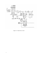
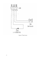
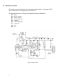
UNINTERRUPTIBLE POWER SYSTEM
SERVICE MANUAL
Blazer series
400VA,600VA and 800VA
Model:
400VA: 400VA/115V,400VA/230V
600VA: 600VA/115V,600VA/230V
800VA: 800VA/115V,800VA/230V
115V/220V/230V/240V 50Hz/60Hz
Prepared by:
Fulin
April 9, 2002
Table of Contents
Chapter
A. Introduction
B. Block Diagram
C. Control Power Circuit
D. Battery Charger
E. Line And Zero-Crossing Detection
F. Inverter Operation
G. Active Clamp
H. Microcontroller(CPU) Control Circuit
I. Displays ,Audio alarm and control button
J. Load Detection Circuit
K. Interface Circuit
L. Troubleshooting
3
Index of Figure
Electrical circuit Schematic diagram
Figure S-1
Figure S-2
Figure S-3
Figure S-4
Figure S-5
Figure S-6
Figure S-7
Figure S-8
Figure S-9
Control Power Circuit
Charger Circuit
Line and Zero Crossing detecting Circuit
Inverter Circuit
CPU Circuit
Relay Circuit
Panel Circuit
Load Detecting Circuit
RS232 Circuit
Waveform & flowchart
Figure W-1 Cold Start
Figure W-2 Zero Crossing
Figure W-3 Inverter Circuit (1)
Figure W-4 Inverter Circuit (2)
Figure W-5 Clamp Circuit
Figure W-6 Relay speed up capacitor
Figure W-7 Battery mode examination flowchart
Figure W-8 Line mode examination flowchart
3
A. Introduction
Blazer series is an off-line power System that has a square wave output. It prevents impulse,
surge, sag and power outage situations. It provides the UPS output load with a reliable
source. It has the following functions:
Booster:
If the commercial line is under voltage, the Booster will rise the UPS output voltage to
1.18 times its input voltage.
2.
Buck:
If the commercial line is over voltage, the Buck will reduce the UPS output voltage to
0.85 times its input voltage.
3.50/60Hz Automatic Frequency Selection:
The output frequency will automatically match the input frequency (50 or 60Hz).
4.Communication Port(RS232+open collector):
Computer interface with RS232 communication and remote shutdown capacities.
5.Data line/telephone line protect:
The unit provides RJ11 receptacles to provide transient voltage surge suppression
(TVSS) for data line or telephone line.
6. Cold start( DC start):
It comes with a DC start feature while without input source.
1.
This manual contains block diagram, principle of operation, system outline and
troubleshooting.
2
B. Block Diagram
The Block diagram of Blazer series (refer to Figure S-1) is divided into the following
parts:
a) Main relay (MAIN-RY):
To switch the UPS between line and battery mode. Its mechanical action also affect
the UPS power loss time.
b) Booster Relay(BOOST-RY):
At line mode, this is a switch used to increase UPS output voltage 18% when the
commercial line source is under voltage.
Relay OFF : line voltage is normal
Relay ON : line voltage is under voltage.
c) Buck Relay:
At line mode, this is a switch used to decrease UPS output voltage 15% when the
commercial line source is over voltage.
Relay OFF : line voltage is normal
Relay ON : line voltage is over voltage.
d) Main Transformer(MAIN TX) :
The Main transformer has three functions:
1. Inverter Transformer
Provides inverter voltage to UPS output. It performs a push-pull transformer when
UPS at battery mode.
2. Booster/Buck
Thus the output voltage at booster mode is given by (Boost Relay ON) :
VOUT = V IN * 1.18
The Buck relay is ON when the line voltage is over voltage. It can reduce output
voltage by:
VOUT = 0.85 V IN
3. Charger :
The Main transformer has a charger coil (TXC) to supply an adequate voltage to
charger circuit.
e) Line Sense
To process the attenuated signal (including input voltage and zero crossing) from rectifier
and send the results to CPU.
b) CPU (NEC µPD78F9116A)
The Central Process Unit
c) Electricity Switch
It controls the 5 Volts and 12 Volts DC supplies. +5Volts and +12Volts Control Power
Generator:
Provide +5Volts (generated from 7805 regulator) and +12Volts DC power supply
d) Charger:
The source for the Charger comes from the charger coil (TXC) of the Main
3
transformer. A traditional linear charging circuit is used for the Blazer series . Regulator
LM317 is used to adjust the battery charging voltage. The charging voltage is 13.3—
14.2V.
g) Inverter circuit :
The inverter circuit is based on a push-pull circuitry to drive inverter transformer
coil .
h) Panel PCB :
The UPS display device contains one led and one switche .
l) Batteries:
Acts as a power supply source while the UPS is at battery mode. Different types of
batteries are used for different models of UPS:
600VA : 12V7Ah *1 pc
400VA : 6V4Ah *2pc
800VA : 1245W*1pc
4
C. Control power circuit
The control power (+12VDC and +5VDC) comes from the following cases(Figure S-2)
1) Start without input AC power (Cold start):
A “Cold start “ is described as follows:
1.
When “ON/OFF” switch(SW1) is depressed, a positive battery current flows through
SW1 to charge C15.
2. Q12 base receives a HI pulse and turn on (signal bypass C15 at t=0 and charge C15 at
t>0).
3. When Q12 turns on, the Q12 collector will drop to LOW and turn on
Q11(MPS2907A).
4. When Q11 turns on ,the positive battery voltage via Q12 collector and establishes
a 12 volt. Power supply. The 12 volts. power supply passes through U03(78L05)
generating a 5 volt DC logic power supply.And CPU send HI signal(shutdown)to
sustain Q12 on.
5. Figure W-1 shows the pulse on the C15,i.e. the base signal of Q12 during the cold
start.
2) Start with input AC power(AC start) :
1. When we connected UPS with AC source, AC voltage pass through fuse ,full wave
rectifier(D21,D22,D23,D24) and ZD02(Zenor diode) turns on Q12.
2. If on/off switch is depressed,As a result Q11 turns on and establishes a 12 volts and 5
volts DC power supply similar to Cold start.
The SHUTDOWN network, triggered by pin 17 of the CPU, is used to shutdown the
UPS from Battery mode. When a battery under-voltage occurs, the CPU sends a Low
signal to turn off Q12. This causes Q11 to be turned off and isolates the control power
from batteries.
5
Figure S-1 Control Power circuit
6
CH1 : C15
GND
Figure W-1 Cold Start
7
D. Battery Charger
The action of charger is described as follows : (Figure S-3)
1. When UPS connected to AC source, the CPU was active because the control power (+5V)
was established.
2. The CPU turned on MAIN RELAY(RY01),AC power flow into Main Transformer.
3. Source for the charging circuit comes from the charger coil of the Main Transformer.
4. A traditional linear charging circuit is used for the UPS. Regulator U02(LM317) is used
to adjust the battery charging voltage. The charging voltage can be set by changing the
value of R28, R27, R29 and R62. The charger voltage is given by
Rp=(R27*R29*R62)/(R27*R29+R29*R62+R62*R27)
VOUT = VREF [1 + Rp/R28] + IA*Rp
IA = 50 µA typical (LM317 A pin offset
current)
Where VREF = 1.25 Volts, which is the voltage drop between LM317 A pin and the
Output pin. Thus the output voltage is
VOUT = 1.25 Volts [1+1050/100] + 50 *10-6 * 1050 = 14.4275 Volts.
( If T=25 degree Rp=(2000*4020*4990)/
(2000*4020+4020*4990+4990*2000)=1.05kohm)
By considering the voltage drop of D13, the actual charging voltage is given by
14.4275-0.7 = 13.7275 VDC
To prevent the charger current from over-charging and damaging the batteries,
R31,Q09 and associated components are used as the current limiter.
The current limiter process is described below. The process repeats itself until the
voltage for R31 drops to turn off Q09.
1.
2.
3.
4.
5.
Q09(2N3906) turns on when current of R31 too large.
Q09 turns on Q08
A (Adjust ) pin of U02(LM317) is pulled down to 0 Volts when Q08 turns on.
As a result the output voltage of LM317 is pulled low from 13.7275V to
approximately 1.25 V causing Q09(VE < VB )and Q08 to be turned off.
This cause the output voltage of LM317 return to 13.7275 V.
The CHG-OFF signal from CPU pin28 is used to turn off charger circuit at battery
mode. The CPU turns on Q08 via sends a HI signal to base of Q08. As a result the charger
be turned off.
8
Figure S-2 Charger circuit
9
E. Line And Zero-Crossing Detection
Please refer Figure S-4
1) Line Detection
The input voltage is full-rectified The signal passes through a voltage divider at R45
and R40//r47,feed into pin 8 of CPU. By monitoring this rectified sinusoidal voltage, the
CPU can find the unnaturalness of commercial line. The CPU has two ways to judge line
voltage loss
1.
Waveform detection:
If there is a rapid voltage drop occurs, the CPU is able to immediately detect it
and transfer to battery mode. The waveform detection has a short response time.
2.
RMS value detection:
CPU calculates input RMS value every cycles. If RMS value is not in range
of UPS specification for 3 cycles ,UPS will transfer to battery mode. The RMS
value detection has a more accurate voltage detection but it can not immediately
sense a rapid voltage transition.
2) Zero Crossing Detection
Zero Crossing Detection is used to minimize the phase difference between the
Inverter voltage and the input line voltage while UPS is switching from battery mode
to line mode. If the phase difference is too large, it can create a large amount of energy
which may damage the internal passive components such as relays.
The Zero Crossing signal is get by the following ways:
1.
2.
Use the voltage reduced from input line voltage(by resistor R49) to drive
Q14(2222ASM).
The Zero Crossing signal comes from the collector of Q14,goes to the CPU pin 1.
Refer to Figure W-2, Waveform measured from Q14 collector and line input.
When the line signal (reduced from input line) is applied to the base of Q14,the first
half cycle(positive half-wave) makes VBE <0 Volts , that turns off Q14. The second half
cycle (negative half-wave) causes VBE >0.5Volts and turns on Q14.
When Q14 is off, the +5 Volts is charging C23. Hence the VCE of Q14 changes from
0 to +5 Volts. As Q14 turns on, C23 discharges immediately. Thus, the line frequency
can be detected by measuring the time interval between the first falling and second falling
edge of VCE of Q14. Also It is used by the CPU to determine when to switch from battery
mode to line mode.
10
Figure S-3 Line and Zero Crossing Detecting circuit
11
CH1 : Line-I/P
CH2 : Q14 collector
Figure W-2 Zero Crossing
12
F. Inverter Operation
The Inverter circuit (Figure S-5) and PWM control are only active under Battery mode.
The Inverter circuit of Blazer is based on a push-pull circuitry and its output is driven by
transistors which is controlled by CPU.
Refer to the Inverter circuit diagram, the DS1(PWM signal ) and DS2 (PWM signal)
signals are generated by CPU. Figure W-3 illustrates the waveforms of DS1 and DS2 while
the system is at no load condition. the duty cycles of DS1 and DS2 signals are controlled by
feedback signal of output voltage (please refer Charger circuit) to get a stable output.
The gates of MOSFETs are driven by transistors Q20,Q24 ,Q23,Q25 which are controlled
by the DS1 and DS2 from CPU pin 11 and 26. Figure W-4 shows the collector waveforms for
transistor pairs Q20,Q24 ,Q23,Q25 while the system is at no load condition.
C24 and R83 are used to eliminate the inverter transformer energy spikes due to the
MOSFET transferring from ON to OFF. First, energy is stored on C27 (through D28 and D29)
until the MOSFET are turned on. This reduces energy spikes which are generated during the
MOSFET power-down period. It also makes sure that the VDS voltage output are not to be
over rated while MOSFET turning off.
13
Figure S-4 Inverter circuit
14
CH1 : DS1
CH2 : Output Voltage (1/200V)
Figure W-3 Inverter Circuit (1)
15
CH1 : DS2
CH2 : Output Voltage (1/200)
Figure W-4 Inverter Circuit (2)
16
G. Active Clamp
The purpose of Clamp circuitry (Figure S-5) is to pull down the output voltage while two
sets of Inverter MOSET are OFF. The Clamp circuitry is active during the period of zero Volt.
of square wave at battery mode.
The Q22 is activated while the CLAMP-OFF signal (from pin 27 of CPU) goes to HI .
If either one of the two MOSFET sets turn on (Q20/Q24 or Q023/Q25), the CLAMP-OFF
signals will remain HI.
When UPS at line mode, the CLAMP-OFF signal remains HI. This turns on U07 to turn
off Q22. At this time the Clamp circuitry is not active. When the CLAMP-OFF is LOW, U07
turns OFF and Q22 turns on. This pulls down output voltage to approximately zero at battery
mode. Figure W-8 illustrates the relationship of the output waveforms and the CLAMP-OFF
signal.
17
CH1 : CLAMP-OFF signal
CH2 : output voltage (1/200V)
Figure W-5 Clamp circuit
18
H. Microcontroller(CPU) Control Circuit
The CPU is supplied by a 5 volts. power supply to pin 25 with ground pin at pin 24. An
extra oscillation circuitry ,(consisting of C03,C04,and crystal XL1) is connected to pin 22
&23. The Blazer series use a CPU type NEC µPD78F9116A and its oscillator frequency is 5.0
MHz.
The pin definition of Blazer CPU is (Figure S-6):
pin 1 : ZERO-CRO control
pin 2 : Buzzer control
pin 3 : SW
pin 4 : +5Volts
pin 5 : load detection
pin 6 : batteryvoltage detection
pin 7 : O/P-V detection
pin 8 : input line detection
pin 9 : ground
pin 10 : no use
pin 11 : inverter PWM signal (DS1)
pin 12 : boost relay control
pin 13 : no use
pin 14 : buck relay control
pin 15 : mani relay control
pin 16 : LED1 control
pin 17 : shutdown
pin 18 : model selection
pin 19 : reset control
pin20 : Vpp (via resistor R11 to ground)
pin 21 : no use
pin 22 : oscillation circuit
pin 23 : oscillation circuit
pin 24 : ground
pin 25 : +5Volts
pin 26 : inverter PWM signal (DS2)
pin 27 : CLMP-OFF control
pin 28 : charge off control
pin 29 : TXD
pin 30 : RXD
To prohibit the CPU from power-up in an unknown state, circuit consisting of Q02 and
associated components, is implemented to force a hardware reset to the CPU whenever the
power is turned on.
Figure S-7 is the relay circuit.The RY01 (main relay) is used for switching between line
and battery modes. When the UPS is changing from battery to line mode, CPU pin 15 is set to
HI to turn on Q03(2SC1815), this actives RY01. Alternatively, if the UPS is changing from
19
line mode to battery mode, CPU pin 15 is set to LOW and turn off Q03. This causes RY01 to
be OFF and return to its normal state.
R16,D02,C10 and Q04 are used to speed up the relay action, so the power loss time can
be reduced to minimum. When UPS transfers to battery mode, C10 is charged by the +12
Volts. After the main relay makes contact, C10provides instantaneous power to the relay coils.
This increase the magnetic force and speeds up the relay to reduce the transfer time from
battery mode to line mode. See Figure W-9 for voltage changes on C10,during line to battery
mode transfers.
CPU pin 12 is used to the drive signal for RY02 (booster relay). When the input line
source voltage falls below boost active threshold, pin 12 sends a high signal to turn on Q05
(2SC1815). This actives the RY02 ,and UPS goes into the Boost mode. When the input line
voltage goes above the boost disactive threshold, the UPS returns to nominal mode by sends
a LOW signal from pin 12. This forces RY02 to switch into its normal position( OFF). At
battery mode, pin 12 is always set to LOW and RY02 is disable.
The same case as buck control, CPU pin 14 is used to the drive signal for RY03 (buck
relay). When the input line source voltage rise above buck active threshold, pin 14 sends
a high signal to turn on RY03. When the input line voltage goes below the buck disactive
threshold, The UPS returns to nominal mode by output a LOW signal from pin 14.
20
Figure S-5 CPU circuit
21
Figure S-6 Relay Circuit
22
CH1 : C10(+) GND
CH2 : Output Voltage (1/200V)
Figure W-6 Relay speed up capacitor
23
I Displays ,Audio alarm and control button
1) Display (Figure S-8)
There are and one led on front panel .
While switch on, CPU sends a HI signal passes through LED to turn on LED.
2) Audio alarm
The buzzer is controlled by pin 2 of CPU. When CPU send a HI signal to buzzer from pin
2, buzzer is beeping. And CPU send LOW signal to stop buzzer.
3) Control button
ON/OFF Button : Push to turn on UPS, push again to turn off UPS (Please refer Chapter
C for cold start & AC start)
24
Figure S-7 Panel circuit
25
J. Load Detection Circuit
The load detecting circuit is showed on Figure S-9. The output current is sensed by
current transformer CT01. It decrease 1000 times of output current for CPU detection. The
current signal decreased from CT01 pass through a full bridge rectifier and across R36 to get
a voltage signal. After the voltage signal divided by R34,R102 to get 0~5 Volts. signal, the
CPU can get output current value of UPS.
1. At line/booster/buck mode : The current value multiplies output voltage to get output VA
value.
2. At battery mode : Because the power factor of square wave is approximately equal 1. The
current value multiplies 120V(230V)output voltage to get output Watt value.
ZD03 is added for protection of rectifier. They can clamp voltage spike while there is a
large current occurs.
Figure S-8 Load Detecting Circuit
26
K. Interface Circuit
The interface circuit (refer Figure S-6) consists three kinds of signal – relay signal, RS232
series communication, and plug & play for Windows 95.
The communication port is a D type 9 pin connector and its pin definition is :
pin1 : N.C
pin2 : RS232 transmit
pin3 : RS232 receive
pin4 : connect with pin 6
pin5 : common
pin6 : connect with pin 4
pin7 : connect PC
pin8 : N.C
pin9 : N.C.
Figure S-9 RS232 circuit
27
L. Troubleshooting
WARNING
1. Troubleshooting can be done by qualified engineer or technician only.
2. Use isolated AC source for your oscilloscope to prevent floating voltage problem between
UPS chassis ground and system reference ground.
3. Before opening the cover, turn off the main switch and unplug the input power cord.
4. Because of some energy will remain in the DC capacitors, wait for at least 5 minutes after
turning off the UPS and disconnecting the power cord before open its cover.
5. Plug in the input power cord before you reconnect the connectors of battery to prevent
unwanted sparks.
Please depend on the following steps when you want to repair a problematic unit :
1. Visual inspection
This is the first step to check the UPS after opening its cover. Be sure to do it, it can help you
to identify with most problems. Major items that should be checked are listed below :
(1) Are there any connectors or terminals loosen ?
(2) Are there any components burn-out or decolored ?
Especially the power components on the heatsink.
(3) Are there any capacitors broken or leakage?
Check all the components listed above and replace which is abnormal.
2. Troubleshooting flowchart
To prevent from damaging yourself and the UPS, be sure to obey the sequences of flowchart
listed below.
28
2.1 Battery mode examination (please refer flowchart)
Procedure :
1 .(1) Replace batteries by DC power supply and turn on it.
(2)Check if there is current limit phenomenon for DC power supply.
2
One or more MOSFETs (Q20,Q23~25) is D-S short. Check and replace it. If
MOSFETs have been replaced once, replace the PCB.
3. Check if both buzzer beeps and LED flash for once.
1. Check if +5V on CPU pin 25 is normal.
2. Check if clock signals on CPU pin 22 and 23 are correct.
3. Replace the CPU. But if the CPU has been replaced once, replace the PCB.
4. Replace abnormal crystal XL1.
5. Check if DC fuse F01 (and F02) are open.
6. Replace abnormal DC fuse.
7. Check if there is a battery voltage on regulator 7805 input.
8. Check Q11 (MPS2907A) ,Q12(2222ASM) and replace them if abnormal.
9. Check there is +12V on 7805 input.
10. Replace abnormal Q11.
11. Check there is +5V on U03 (7805)
12. Replace abnormal 7805.
13. Replace PCB
14. Check if buzzer beeps and LED extinguished.
15. Check if battery voltage is correct.
16. Replace abnormal batteries.
17. Check D17 if it is open.
18. Replace abnormal Diode.
19. Replace PCB.
20. Buzzer beeps and LEDs flash .
21. Check if fault LED lights and buzzer beeps continuously.
22. Check if CPU is shorted.
23. Replace abnormal CPU.
24. Check if Q22 (RFP50N06) is shorted.
25. Replace abnormal RFP50N06.
26. Check if Q07 is failed.
27. Replace abnormal Q07.
28. Replace PCB.
29
2.2 Line mode examination (please refer flowchart)
If battery mode procedure are OK then check the following procedure.:
Procedure :
1 (1)Plug in input power cord at right voltage range.
Check if mani relay RY01 are active (230/240V models).
(2)
Check UPS if remains at line mode (for 120V models).
(1)
2. Check if input fuse is open.
1. Replace fuse.
4. (1)Replace main relay(230/240V models).
Turn to procedure (6) (120V models)
(2)
5. Check UPS if remains at line mode.
1. Check if full bridge rectifier is short.
2. Replace abnormal diode
3. Check Q14 (2222ASM collector) if there is zero crossing signal.
4. Replace abnormal Q14.
5. Replace PCB.
6. Check if buzzer beeps continuously and fault LED lights.
7. Check if main relay (RY01) is bad.
8. Replace abnormal main relay (RY01).
9. Replace PCB.
30
Figure W-7 Battery mode examination flowchart
Figure W-8 Line mode examination flowchart
30