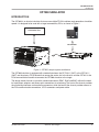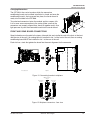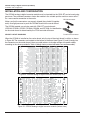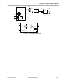
1
OP7000 Simulator User Guide www.opal-rt.com Published by OPAL-RT Technologies, Inc. 1751 Richardson, suite 2525 Montreal, Quebec, Canada H3K 1G6 www.opal-rt.com © 2015 OPAL-RT Technologies, Inc. All rights reserved Printed in Canada SYMBOL DEFINITIONS The following table lists the symbols used in this document to denote certain conditions: Symbol Definition ATTENTION: Identifies information that requires special consideration TIP: Identifies advice or hints for the user, often in terms of performing a task REFERENCE _ INTERNAL: Identifies an additional source of information within the bookset. CAUTION Indicates a situation which, if not avoided, may result in equipment or work (data) on the system being damaged or lost, or may result in the inability to properly operate the process. Indicates a situation where users must observe precautions for handling electrostatic sensitive devices. ! CAUTION: Indicates a potentially hazardous situation which, if not avoided, may result in minor or moderate injury. It may also be used to alert against unsafe practices. ! WARNING: Indicates a potentially hazardous situation which, if not avoided, could result in serious injury or death. OP7000 User Guide Opal-RT Technologies iii CONTENTS OP7000 SIMULATOR............................................................................................................................... 9 INTRODUCTION................................................................................................................................... 9 DESCRIPTION.................................................................................................................................... 10 Standard and Optional Boards....................................................................................................................................... 11 OP7000 front interface....................................................................................................................................12 OP7000 rear interface.....................................................................................................................................13 Installation and Configuration ..........................................................................................................................14 receiving and verification...................................................................................................................................14 Standard Hardware........................................................................................................................................................ 14 basic system cabling. .........................................................................................................................................14 connecting monitoring devices...........................................................................................................................14 power-up procedure..........................................................................................................................................15 OP7161 FPGA BOARD....................................................................................................................... 16 OP7220 CARRIER BOARD................................................................................................................. 17 monitoring interface..........................................................................................................................................17 RJ45 Monitoring Connectors......................................................................................................................................... 17 RJ45 Channel Assignments .......................................................................................................................................... 17 Installing a New Board................................................................................................................................................... 18 Changing Mezzanines.................................................................................................................................................... 19 front and rear board connections.....................................................................................................................19 op7220 communication diagram...........................................................................................................................20 OP7461 PCIE BOARD......................................................................................................................... 21 . ..........................................................................................................................................21 circuit layout diagrams......................................................................................................................................21 module installation OP7000 SPECIFICATIONS................................................................................................................. 22 special notes.....................................................................................................................................................22 OP5330 DIGITAL TO ANALOG CONVERTER ...................................................................................... 23 DESCRIPTION.................................................................................................................................... 23 requirements.....................................................................................................................................................23 Software......................................................................................................................................................................... 23 Hardware........................................................................................................................................................................ 23 features. ...........................................................................................................................................................23 offset and gain calibration. ...............................................................................................................................23 MODULE INSTALLATION AND CONFIGURATION ........................................................................... 24 circuit layout diagrams......................................................................................................................................24 SCHEMATICS...................................................................................................................................... 25 TYPICAL APPLICATIONS................................................................................................................... 25 OP7000 User Guide OPAL-RT Technologies 5 OP5340 ANALOG TO DIGITAL CONVERTER (0.5 MSPS)................................................................... 27 DESCRIPTION ................................................................................................................................... 27 requirements.....................................................................................................................................................27 Software......................................................................................................................................................................... 27 Hardware........................................................................................................................................................................ 27 features. ...........................................................................................................................................................27 offset and gain calibration. ...............................................................................................................................27 INSTALLATION AND CONFIGURATION............................................................................................. 28 circuit layout diagrams......................................................................................................................................28 SCHEMATICS...................................................................................................................................... 29 input gain selection . .........................................................................................................................................29 input gain calculations.......................................................................................................................................30 OP7353 DIGITAL MONITORING BOARD.............................................................................................. 33 DESCRIPTION ................................................................................................................................... 33 circuit layout diagrams......................................................................................................................................33 OP7811 PASSTHROUGH MODULE...................................................................................................... 35 DESCRIPTION ................................................................................................................................... 35 INSTALLATION.................................................................................................................................... 35 circuit layout diagram........................................................................................................................................35 connector pin assignments.................................................................................................................................36 SPECIFICATIONS............................................................................................................................... 36 OP7816 16 DIN SIGNAL CONDITIONING MODULE............................................................................ 37 DESCRIPTION ................................................................................................................................... 37 features. ...........................................................................................................................................................37 INSTALLATION.................................................................................................................................... 37 MODULE IDENTIFICATION AND INITIALISATION............................................................................. 38 circuit layout diagram........................................................................................................................................38 input interfaces.................................................................................................................................................38 TYPICAL APPLICATIONS................................................................................................................... 39 connector pin assignments.................................................................................................................................41 SPECIFICATIONS............................................................................................................................... 41 OP7817 16 DOUT SIGNAL CONDITIONING MODULE........................................................................ 43 DESCRIPTION.................................................................................................................................... 43 features. ...........................................................................................................................................................43 INSTALLATION ................................................................................................................................... 43 MODULE IDENTIFICATION AND INITIALISATION............................................................................. 43 circuit board layout diagrams. ...........................................................................................................................44 OP7817 PIN ASSIGNMENTS ................................................................................................................ 45 37 connector ...............................................................................................................................................45 db GENERAL SPECIFICATIONS............................................................................................................. 45 ELECTRICAL SPECIFICATIONS........................................................................................................ 46 5 V Option...................................................................................................................................................................... 46 12 V Option.................................................................................................................................................................... 46 24 V Option.................................................................................................................................................................... 46 6 OPAL-RT Technologies OP7000 User Guide OP7818 16 AIN SIGNAL CONDITIONING MODULE............................................................................ 47 DESCRIPTION ................................................................................................................................... 47 features. ...........................................................................................................................................................47 INSTALLATION ................................................................................................................................... 47 MODULE IDENTIFICATION AND INITIALISATION............................................................................. 48 circuit layout diagrams......................................................................................................................................48 jumper and switch positions...............................................................................................................................49 optional mezzanine board ..................................................................................................................................50 TYPICAL APPLICATION DIAGRAMS.................................................................................................. 51 voltage mode diagram.........................................................................................................................................51 current mode diagram........................................................................................................................................51 Resistive Sensor Mode Diagram.................................................................................................................................... 52 CONNECTOR PIN ASSIGNMENTS.................................................................................................... 54 SPECIFICATIONS............................................................................................................................... 54 OP7832 SYNCHRONIZATION MODULE............................................................................................... 55 DESCRIPTION ................................................................................................................................... 55 features. ...........................................................................................................................................................55 INSTALLATION.................................................................................................................................... 56 USER INTERFACES............................................................................................................................ 56 status leds . ......................................................................................................................................................56 connectors........................................................................................................................................................57 circuit layout diagram........................................................................................................................................58 SPECIFICATIONS............................................................................................................................... 58 SPECIFICATIONS ................................................................................................................................. 59 OP7000 SIMULATOR SPECIFICATIONS............................................................................................ 59 OP5330 DIGITAL TO ANALOG CONVERTER.................................................................................... 59 OP5340 ANALOG TO DIGITAL CONVERTER.................................................................................... 60 OP7353 16 CHANNEL DIGITAL MONITORING (FRONT).................................................................. 61 OP7812 16 DIGITAL INPUTS.............................................................................................................. 61 TROUBLESHOOTING .......................................................................................................................... 63 LIMITED WARRANTY............................................................................................................................. 65 limited warranty................................................................................................................................................65 return policy.....................................................................................................................................................65 exclusions.........................................................................................................................................................65 warranty limitation and exclusion.......................................................................................................................66 .....................................................................................................................66 ..........................................................................................................................................66 disclaimer of unstated warranties limitation of liability OP7000 User Guide OPAL-RT Technologies 7 8 OPAL-RT Technologies OP7000 User Guide OP7000 Simulator Introduction OP7000 SIMULATOR INTRODUCTION The OP7000 is an ultrafast simulator that can use multiple FPGA to achieve next generation simulation speed. It is designed to be used with a target connected by PCIe, as shown in Figure 1. Unit Under Test HOST COMPUTER Ethernet Hub PCIe Target OP7000 Figure 1: OP7000, sample system architecture The OP7000 simulator is equipped with standard interfaces: the OP7160-1 (130T) or the OP7161-1 (240T) are the primary FPGA boards that occupy the center slot in the chassis and the OP7461 is the PCIe communication board that connects the OP7000 simulator to the target. The design makes it easier to use with standard connectors (DB37, RJ45 and BNC) without the need for input/output adaptors and allows quick connections for monitoring. The front of the chassis provides the monitoring interfaces and monitoring connectors, while the back of the chassis provides access to the PCIe communication connections, all I/O connectors and power cable. OP7000 User Guide OPAL-RT Technologies 9 OP7000 Simulator Description DESCRIPTION The OP7000 is available in a number of different configurations that make it easier to integrate into your environment. Select any combination of signal condtioning boards (up to 16 DI/O, 8 AI/O or a combination of 8 DI/O and 4 AI/O) or select up to 8 FPGA secondary boards (for pure computation with no I/Os). Figure 2: OP7000 (front) The rear of the OP7000 contains the connectors for the PCIe link to the target and for signal conditioning from the target and to the unit under test. Figure 3: OP7000 (rear) 10 OPAL-RT Technologies OP7000 User Guide OP7000 Simulator Description Standard and Optional Boards The front section contains the carrier boards and conditioning modules with connectors for monitoring and the rear section contains conditioning boards for connections from the unit under test. FRONT BOARDS OP7220 DESCRIPTION REAR BOARDS ANALOG I/Os Universal Carrier OP7811 with OP5330 or OP5340 mezzanine card OP7818 - 2 DESCRIPTION Required for use of back analog IO cards OP7000_Rear_Interface_DB37 (Passthrough) OP7000 Rear Analog Input conditioning for OP5340, Voltage or Current mode, 16ch DB37 connectors OP7000 Rear Analog Output conditioning for OP5330, Voltage or Current mode, 16ch DB37 connectors OP7000_6U_AIO_Carrier_DB37 for Type E Modules (Max of 4 modules per carrier) OP7819 - 2 OP78E0 DIGITAL I/Os OP7816 - 2 OP7353 or OP7161-2 OP7817 - 2 Secondary V6 (240T) (slots 9, 11, 13 only) OP7820 For distributed FPGA simulations OP7821 In most cases, the corresponding back IO card OP7822 is driven by the Primary FPGA OP7823 OP7824 Primary V6 (130T or 240T) OP716X-1 OP7832 OP7461 OP7000 Rear Opto-Isolated Digital Input : 16-Din DB37 connector OP7000 Rear Opto-Isolated 16-Dout, PushPull 5V to 30V, DB37 connector OP7000 Rear 8TX and 8RX DC to 50 MBd Fiber Optic link, 650nm OP7000_Rear_16Dout_SSR_250V_200mA (Normaly Open Relay) OP7000_Back_6TX_6RX_Fiber_Optic_ link_820nm OP7000 Rear 16RX DC to 50 MBd Fiber Optic link, 650nm OP7000 Rear_16TX_DC_to_50_MBd_Fiber_ Optic_link_650nm OP7000 Rear Synchronization card (Between OP7000, OP5600 , Wanda, …) Communication Interface PCIe 4X (match with 126-0347) Table 1: OP7000 board type pairings *The OP7161 and OP7461 boards are the core of the OP7000 and are not optional. Consult your sales representative for the complete list of available signal conditioning boards. NOTE Boards used in the back of the unit must correspond to the type of boards used in the front. Example: if an Analog Out board is used in front slot #1, then a matching Analog out board must be used in the rear slot #1. OP7000 User Guide OPAL-RT Technologies 11 OP7000 Simulator Description OP7000 front interface The interfaces provided on the OP7000 simulator may vary depending on the system configuration. A B C A4 A3 A2 SIGNAL MONITORING WITH GAIN OF 0.1 SIGNAL MONITORING WITH GAIN OF 0.1 D Figure 4: OP7000 front connector panels A. Power switch with LED indicator. B. Carrier board (OP7220) interfaces: -- 16 red LEDs (8 pairs). Light intensity is directly commensurate to voltage (the higher the voltage, the brighter the LED intensity)1. -- One Status LED with variable color (see table for display description) LED Red Description Insufficient power voltage for digital board. Blinking red Insufficient power voltage for analog board Blinking orange No upload of mezzanine. Orange Sanity signal absent Yellow All statuses normal. Blinking yellow Error in analog board even slot Table 2: Carrier board LED functions -- One column of 4 RJ45 connectors provide connections to monitor output from mezzanine I/O boards. Each connector represents 4 channels (see “Installation and Configuration” for more detailed information). 1 LED threshhold is 1V 12 OPAL-RT Technologies OP7000 User Guide OP7000 Simulator Description C. Monitoring connectors D. FPGA board: -- JTAG connector for programming functions. Reserved for OPAL-RT technicians’ use only. -- One RJ45 connector. DISABLED, for OPAL-RT’s technicians’ use only. -- 7 LED indicators: Position LED Description 1 Power On (green) indicates that the unit is powered up. 2 Config Green indicates that a user defined configuration (bitsream) is running. Yellow indicates that the safe, default configuration (bitsream) is running. Flashing indicates the configuration is paused. Off indicates that there is no configuration available.. 3 Comm On (green) indicates communication with the PC is in progress. 4 Model On indicates model in use. 5 Sync Green indicates Master synchronisation in progress Yellow indicates Slave synchronisation in progress 6 Fault Red indicates a fault. 7 User defined functions Green/Yellow Table 3: FPGA board LED functions OP7000 rear interface The connectors on rear modules are DB37F by default. BNC may be installed on custom boards and must be specified at the time of the order. A B C D Figure 5: OP7000 rear connector panels A. B. C. D. DB37F I/O connectors and status LEDs (see each board’s pin assignments section for details). PCIe communication connector. Synchronization board (to synchronize with external OP5600, OP7000 chassis) Power connection port and ground screw. OP7000 User Guide OPAL-RT Technologies 13 OP7000 Simulator Description INSTALLATION AND CONFIGURATION This section provides a description of the hardware included withthe basic simulation system (with the OP7000 at its core) and how to connect the various cables between devices. Before beginning to install your system, verify that all the standard (and optional) components are present. receiving and verification After opening the package, remove the equipment and components. Make sure that all the items described in “Standard Hardware” are actually in the box and are undamaged. Standard Hardware The OP7000 real-time simulator includes the following basic hardware: Item Description Part Number OP7000 simulator Simulator FPGA and PCIe boards and any other optional boards N/A RT-LAB software CD O/S CD (Redhat or QNX) Documentation CD N/A RJ45 cables (4) 61cm (24”) RJ45 cables C-02B-CAT6 Power cable 1.83 m (6’) power cord, black (10A 125V) CPC06 OPAL-RT target System Integration binder PCIE cable BNC cables (4) OPAL-RT strongly recommends the use of anti-static wrist straps whenever handling any electronic device provided by OPAL-RT. Damage resulting from electrostatic charges will not be convered by the manufacturers warranty. basic system cabling The design of the simulation system includes quick, standardized I/O connections (either BNC or DB37F) and RJ45 connections for monitoring each channel individually. The simulator is preconfigured according to your specifications and installation is as easy as mounting the simulator and connecting the appropriate cables from the simulator to the target. connecting monitoring devices The OP7000 simulator offers quick, single-ended connections, through RJ45 and BNC connectors, to any monitoring device (i.e. oscilloscope, etc.). These BNC jacks let you monitor 4 channels individually. Simply follow these instructions (as illustrated in Figure 6): CAUTION 14 Only connect RJ45 cables from upper section (A) monitoring jacks to lower section monitoring panel (B, as shown). Connecting any other cable or device may result in damage to the equipment. OPAL-RT Technologies OP7000 User Guide OP7000 Simulator Description A B C AUTORANGE SAVE/RECALL MEASURE UTILITY CURSOR ACQUIRE HELP DISPLAY DEFAULT SETUP REF MENU AUTOSET RUN/ STOP SINGLE SEQ SAVE PRINT CH 1 MENU MATH MENU CH 2 MENU HORIZ MENU TRIG MENU SET TO ZERO SET TO 50% FORCE TRIG TRIG VIEW D Figure 6: How to connect cables for monitoring 1. Connect one end of the RJ45 cable to the desired channels (A). 2. Connect the other end of the RJ45 cable to the monitoring connector (B) 3. Connect a BNC cable to a BNC jack (C) and connect the other end of the cable to the desired monitoring device. The BNC jacks each connect to one of the 4 channels of the RJ45 Connector (A). In the example shown in Figure 10, the RJ45 cable is connected to channels 00-03. The miniBNC cable jacks, identified as A, B, C, D, represent each channel in the following order; A = channel 0, B = channel 01, C = channel 02, D = channel 03 (see Figure 10 for illustration). 4. Connect a mini BNC cable to the desired channel and connect the other end to your monitoring device (oscilloscope shown, D). ATTENTION Buffer amplifiers have a Gain of 0.1. power-up procedure The following sequence must be respected to ensure that the system functions properly: 1. Ensure that power cables from the OP7000 and other devices are connected to grounded, protected (see red lable on power cable). 2. Ensure that the PCIe cable is connected to both the back of the OP7000 and the real-time PC. 3. Turn the OP7000 ON 4. Plug the real-time computer network cable in the Ethernet hub. 5. Turn the real-time computer ON OP7000 User Guide OPAL-RT Technologies 15 OP7000 Simulator OP7161 FPGA Board OP7161 FPGA BOARD This board is essentially a digital I/O driver. The FPGA signals drive signal conditioning hardware (consult your custom system integration documentation for the list of boards included with your simulator), other communication hardware and all dedicated hardware using SPI or other interfaces. The centre FPGA is the main component of the OP7000 and must be used with the FPGA mezzanine. However, if additional FPGA boards (secondary) are used in the OP7000, these additional boards do not require the FPGA mezzanine. Figure 7: OP7161-1 primary FPGA board, with mezzanine Figure 8: OP7161-2 seconday FPGA board, without mezzanine 16 OPAL-RT Technologies OP7000 User Guide OP7000 Simulator OP7220 Carrier Board OP7220 CARRIER BOARD The OP7220 carrier board is a part of the OP7000 series of modules for OPAL-RT’s state of the art OP7000 simulator. It is designed for use with OPAL-RT’s mezzanine signal conditioning boards (OP5330, OP5340). The OP7220 provides the interface required for the mezzanine signal conditioning board to communicate with the FPGA board (see “op7220 communication diagram”). The carrier board also provides the connectors that allow monitoring of individual channels and a series of LED indicators to display the status for the condition boards. monitoring interface RJ45 Monitoring Connectors Each front mezzanine interface has a column of RJ45 connectors, representing all 16 channels divided into 4 channels per jack, as shown in Figure 9. Signal Conditioning Board Monitoring Connectors 0 P72Car2rier O Universal ls ChanneStatus 0 1 2 3 4 5 6 7 9 10 11 12 13 14 15 0-3 Channels 0-3 4-7 Channels 4-7 8-11 Channels 8-11 12-15 Channels 12-15 Figure 9: Carrier board RJ45 connections RJ45 Channel Assignments Each of the carrier’s RJ45 connectors, (shown in Figure 9) can be connected to the BNC monitoring connectors on the front of the OP7000 that enable single channel monitoring, as illustrated below. BNC Channel Monitoring Connectors Channels 0-3 Ch 03 Ch 07 Ch 02 Ch 06 Ch 01 Ch 00 Ch 05 Channels 8-11 Ch 08 Ch 09 Ch 10 Ch 11 Ch 12 Ch 13 Ch 14 Ch 15 Ch 04 Channels 4-7 Channels 12-15 Buffer Amplifiers with Gain of 0.1 Figure 10: RJ45 channel assignments OP7000 User Guide OPAL-RT Technologies 17 OP7000 Simulator OP7220 Carrier Board adding boards OPAL-RT strongly recommends the use of anti-static wrist straps whenever handling any electronic device provided by OPAL-RT. Damage resulting from electrostatic charges will not be covered by the manufacturers warranty. Depending on your specific needs, you may wish to install additional conditioning or FPGA boards in the OP7000 simulator. The front of the simulator contains designated slots for a total of 8 additional boards (the centre slot is reserved for the main FPGA board). Slots are color coded to indicate the type of board that can be installed in the front: Yellow: Odd numbered slots can accept OP7220 carrier boards, OP7353 digital monitoring board and FPGA boards (maximum 8 boards). When these slots are used, the next (even numbered) slot on the right cannot be used. Black: Even numbered slots. Only OP7353 digital monitoring boards can be installed (maximum 8 boards). Installing a New Board 1. 2. 3. 4. Disconnect simulator power supply. Remove blank plate from desired slot. Insert desired mezzanine board on carrier board (optional, see “Changing Mezzanines”). Gently slide new board into slot until locking tab clicks into place and connector slides snugly into the connector on the midplane (see Figure 12 and Figure 13). 5. Reconnect power supply. The following image illustrates how simple it is to insert hardware components into the OP7000 chassis. Figure 11: Inserting the carrier board CAUTION 18 The system must be powered down before changing boards. Failure to do so may damage the equipment. OPAL-RT Technologies OP7000 User Guide OP7000 Simulator OP7220 Carrier Board Changing Mezzanines The OP7220 is the carrier board on which the mezzanine conditioning boards are installed. Installation is simple and once the conditioning board is firmly pressed into place, the carrier board is ready to be installed in the OP7000. Two polarized connectors fasten the module and four screws affix it for a more secure connection to the carrier. Make sure that the connectors are properly aligned; they should fit together easily. Use light pressure to push the mezzanine board into the carrier board. front and rear board connections Special attention must be paid to the types of boards that are installed in each of the slots at the front and the rear of the unit. If an analog board is installed in slot 1 at the front of the unit, then an analog conditioning board MUST be installed in slot 1 at the rear of the unit. Each slot has a track that guides the board into the exact alignment for the connector Front carrier board Midplane Back conditioning board Figure 12: Connecting boards to midplane Midplane connectors side view Front connector face view Rear connector face view Figure 13: Midplane connectors - face view OP7000 User Guide OPAL-RT Technologies 19 OP7000 Simulator OP7220 Carrier Board op7220 communication diagram The universal carrier connections allow signals to travel from front to back, in from and returning out to external devices. These signals travel according to a specific architecture, as shown in Figure 14. TO STATUS LEDs & MONITORING CONNECTORS TO/FROM FPGA TO/FROM REAR BOARD Connector face view TO/FROM REAR BOARD Figure 14: OP7220 connection flow Consult the “OP7000 board type pairings” on page 11 section for details on rear channel to pin associations. Consult the”monitoring interface” section for details on front channel to connector associations. 20 OPAL-RT Technologies OP7000 User Guide OP7000 Simulator OP7220 Carrier Board OP7461 PCIE BOARD This board is required to use the OP7000; it creates the communication link between the front FPGA board and the real-time computer running the RT-LAB model. module installation The OP7461 PCIe Module must be inserted into the appropriate slot in the rear of the OPAL-RT simulator, the slot that corresponds to the front FPGA board. Make sure that the card is properly aligned, using the guide tracks, before pressing into place. circuit layout diagrams Figure 15: OP7461 PCIe communication module OP7000 User Guide OPAL-RT Technologies 21 OP7000 Simulator OP7000 Specifications OP7000 SPECIFICATIONS Product name OP7000 Simulator Power supply Universal input and active power factor correction 650W continuous power DC to DC converters for analog voltage I/O connectors See the specfications for each board. Monitoring connectors RJ45 on front modules RJ45 and mini-BNC on OP7000 front panel Dimensions (HxWxD) 26.67 x 48.26 x - cm (10.5” x 19” x “) Weight 9 to 14 Kg, depending on options installed. Operating temperature 10 to 40 ºC (50 to 104ºF) Storage temperature -55 to 85ºC (-67 to 185ºF) Relative humidity 10 to 90% non-condensing Maximum altitude 2000 m (6562 ft.) special notes NOTE: 22 • The OP7000 can only be used with RT-LAB version 10.4.0. If your version of RT-LAB is older than 10.4.0, you will need to update the software. • OP7160/OP7161 Board Index values may differ between RT-LAB 10.4.0, RT-LAB 10.4.9 and RT-LB 10.5.0 • Defaut value, when no OP7832 is present, is 255 in RT-LAB 10.5.0, instead of 31 in RT-LAB 10.4.9 and 0 in RT-LAB 10.4.0. • Actual values when OP7832 is present will depend on the rotary switch position. • The O716x OpCtrl blocks in your models may need to be updated when updating RT-LAB. OPAL-RT Technologies OP7000 User Guide OP5330 Digital to Analog Converter Description OP5330 DIGITAL TO ANALOG CONVERTER DESCRIPTION The OP5330 digital to analog converter (DAC) provides 16 single-ended digital output channels. Each channel uses a 16-bit resolution digital-to-analog converter. It is a part of the OP5000 series of optional modules for OPAL-RT’s state of the art HIL (hardware-in-the-loop) systems, intended for use with OPAL-RT carrier boards (OP5130, OP5220, OP5222, OP5600, OP6228). Each OP5330 can sample up to 1 MS/s, giving a total throughput of 8 MS/s, all channels are simultaneously sampled. The onboard EEPROM provides offset and gain data adjustment written during the calibration process, as well as over-voltage protection. By default, the maximum output signal is set to ±16 volts. requirements Software • RT-LAB 8.4.0 and higher Hardware • OPAL-RT simulator: -- OP7000 series simulator -- OP5600 series simulator -- OP5000 series of hardware-in-the-loop simulators -- OPAL-RT I/O expansion box (only for use with OPAL-RT simulators) • OPAL-RT carrier board: -- OP5130, OP5220, OP5222, OP5600, OP6228, OP7220 features • • • • • 16 single-ended analog output channels All outputs are sampled simultaneously at up to 1 MS/s 16 bit resolution ±15 V voltage range output ±15 mA maximum current per channel offset and gain calibration The OP5330 contains a serial EEPROM to store the module identification, calibration information and other important information. Each OP5330 is factory calibrated after assembly; during calibration, gain and offset are adjusted to ensure accurate target output values at ±20 mV noise and offset. 23 OPAL-RT Technologies OP7000 Ultrafast Simulator User Guide OP5330 Digital to Analog Converter Module Installation and Configuration MODULE INSTALLATION AND CONFIGURATION The OP5330 digital to analog converter must be inserted into the OPAL-RT carrier board using great care. Two polarized connectors fasten the module in the suitable position and four screws affix it for a more secure connection to the carrier. OP5330 connector Make sure that the connectors are properly aligned; they should fit together easily. Use light pressure to push the OP5330 board into the carrier board. The OP5330 module can only be used with OPAL-RT’s carrier boards (OP5130, OP5220, OP5222, OP5600, OP6228 and OP7220). Its identification on the carrier board is determined by the FPGA controller bitstream. Carrier board connector circuit layout diagrams When the OP5330 is installed on the carrier board, only the top of the circuit board is visible, as shown in Figure 16. The connectors are located on the bottom of the board (see Figure 17) and fit snugly into the connectors on the carrier. Figure 16: OP5330 module (top view) Connector Figure 17: OP5330 module (bottom view) OP7000 Ultrafast Simulator User Guide OPAL-RT Technologies 24 OP5330 Digital to Analog Converter Typical Applications SCHEMATICS Figure 18 represents a simplified schematic of one OP5330 module channel. It is composed of three stages: the first stage consists of one gain DAC and one offset DAC; the second stage consists of a signal DAC with an operational amplifier that allows for gain adjustments; the third stage consists of an operational amplifier that receives final signal value and integrates the offset. STAGE 2 STAGE 1 SIGNAL DATA GAIN DATA STAGE 3 VREF SIGNAL DAC - GAIN DAC OUTPUT + + GND - OFFSET DATA + OFFSET DAC OUTPUT + GND Figure 18: Output DAC circuit TYPICAL APPLICATIONS The following diagram provides an example of a typical application using the OP5330. Figure 19: OP5330 typical application 25 OPAL-RT Technologies OP7000 Ultrafast Simulator User Guide OP5340 Analog to Digital converter (0.5 MSPS) Description OP5340 ANALOG TO DIGITAL CONVERTER (0.5 MSPS) DESCRIPTION The OP5340 Analog to Digital converter (ADC) is a part of the OP5000 series of optional modules for OPAL-RT’s state of the art HIL (hardware-in-the-loop) systems, intended for use with OPAL-RT carrier boards (OP5130, OP5220, OP5222, OP5600, OP6228). Designed for OPAL-RT’s simulation systems, the OP5340 converts analog signals to digital. Each ADC can sample up to 500 kS/s, giving a total throughput of 8 MS/s, all channels are simultaneously sampled. The on-board EEPROM provides offset and gain data adjustment written during the calibration process, as well as over-voltage protection. The OP5340 module provides 16 differential analog input channels. Each channel uses a 16bit resolution analog-to-digital converter. The OP5340 module also has input signal conditioning capabilities that allow the user to apply a signal range from ±20v up to ±120v on the inputs. By default, the maximum input signal is set to ±20 volts. requirements Software • RT-LAB 8.4.0 and higher Hardware • OPAL-RT simulator: -- OP7000 series simulator -- OP5600 series simulator -- OP5000 series hardware-in-the-loop simulator -- OPAL-RT I/O expansion box (only for use with OPAL-RT simulators) • OPAL-RT carrier board: -- OP5130, OP5220, OP5222, OP5600, OP6228, OP7220 features • • • • • • 16 differential analog input channels All inputs are sampled simultaneously at up to 500 kSPS 16 bit resolution 500 KΩ input impedance ±20 V input voltage range ±240 input range up to 120V offset and gain calibration The OP5340 contains a serial EEPROM to store the module identification, calibration information and any other important information. Each OP5340 module is calibrated after assembly; during calibration, gain and offset are adjusted to ensure accurate target output values at ±20 mV noise and offset. OP7000 User Guide OPAL-RT Technologies 27 OP5340 Analog to Digital converter (0.5 MSPS) Installation and Configuration INSTALLATION AND CONFIGURATION The OP5340 analog to digital converter module must be inserted into the OPAL-RT carrier board using great care. Two polarized connectors fasten the module in the suitable position and four screws affix it for a more secure connection to the carrier. OP5330 connector Make sure that the connectors are properly aligned; they should fit together easily. Use light pressure to push the OP5340 board into the carrier board. The OP5330 module can only be used with OPAL-RT’s carrier boards (OP5130, OP5220, OP5222, OP5600, OP6228 and OP7220). Its identification on the carrier board is determined by the FPGA controller bitstream. Carrier board connector circuit layout diagrams When the OP5340 is installed on the carrier board, only the top of the circuit board is visible, as shown in Figure 20. The connectors are located on the bottom of the board (see Figure 21) and fit snugly into the connectors on the carrier board. Users may add resistors to change voltages for specific needs, according to the values provided in Table 4 (though factory customized orders are recommended). Figure 20: OP5340 analog to digital converter module (top view) Figure 21: OP5340 Analog to digital converter module (bottom view) 28 OPAL-RT Technologies OP7000 User Guide OP5340 Analog to Digital converter (0.5 MSPS) Schematics SCHEMATICS Figure 22 represents a simplified schematic of one OP5340 module channel. It is composed of three stages: the first stage consists of one operational amplifier that works in differential input mode and permits gain adjustment; the second stage, the level shifter, forms the signal for the A/D converter input; the third stage occurs after the conversion to the digital type, as the signal is sent to the carrier board. Differential Amplifier V in Level Shifter - A / D Converter - + VREF VIN + OUT Serial Data Out REF VREF Figure 22: Differential input ADC circuit input gain selection Optional - for advanced users. The OP5340 module has user selectable input attenuation ability. By default, the maximum input voltage range is set to ±20 volts but each channel can be changed separately up to ±120 volts. The OP5340 module contains resistor networks that allow insertion of additional precision resistors to change the input attenuation. The image on the right shows the placement for the additional resistors. Ch 00 Please refer to the table at the end of this section for the exact relationship between channels and resistors. The next diagram illustrates the input stage of one channel. The default values for resistors R1 and R2 were chosen to keep the maximum input voltage range of ±20 volts (40 volts) with no additional resistors. R1 Vin full range = ±20 volts Vout full range = ±1 volt (2 volts) Installed resistors: R1 = 499 kΩ R2 = 25 kΩ R2 VOUT VIN Vout Formula R1 R2 Vout Vin R1 R2 The factory installed surface mount resistors on the OP5340 module give an attenuation of 20. Vin 1 / 20 OP7000 User Guide Vout OPAL-RT Technologies 29 OP5340 Analog to Digital converter (0.5 MSPS) Schematics input gain calculations The figures below show the complete circuit with resistor Rx as the axial insertable resistor by the user. Input Gain Schematic with Rx Rx R1 - V IN + R1 R2 V OUT R2 Rx Figure 23: Input gain with Rx Vout Formula with Rx R 2 Rx Vout Vin R1 R 2 Rx Vout Formula, with Default R Values and Rx R1= 499K, R2= 25K 1 Rx Vout Vin 2 0 25 Rx Figure 24: Vout formulas Users may define the input gain value and calculate the corresponding Rx resistor value. Table 4 provides maximum range values and associated Rx resistor values (chosen in 0.1% series range). To yield the same unit of measurement, the model must compensate for any new gain value different from the original gain of 1/20. The last column provides the gain to insert in the input signal of the simulation model. Input gain Max voltage input Rx value 0.1% series range Gain to insert in the model 1/20 ±20V (or 40V) none 1 1/40 ±40V (or 80V) 24.9 kΩ 2 1/60 ±60V (or 120V) 12.4 kΩ 3 1/80 ±80V (or 160V) 8.25 kΩ 4 1/100 ±100V (or 200V) 6.20 kΩ 5 1/120 ±120V (or 240V) 4.99 kΩ 6 Table 4: Maximum Range and Resistor Values Example: an added Rx resistor of 4.99 kΩ in parallel with R2 resistor gives an attenuation of approximately 120 so the input voltage can be increased to ±120 volts (or 240 volts). 30 OPAL-RT Technologies OP7000 User Guide OP5340 Analog to Digital converter (0.5 MSPS) Schematics Table 5 shows the relationship between channel and resistor references used for the input gain changes. Channel # Resistor Rx Channel # Resistor Rx Channel 00 R164, R165 Channel 08 R172, R173 Channel 01 R180, R181 Channel 09 R188, R189 Channel 02 R166, R167 Channel 10 R174, R175 Channel 03 R182, R183 Channel 11 R190, R191 Channel 04 R168, R169 Channel 12 R176, R177 Channel 05 R184, R185 Channel 13 R192, R194 Channel 06 R170, R171 Channel 14 R178, R179 Channel 07 R186, R187 Channel 15 R193, R195 Ch 00 Table 5: Resistor Network Channel Identification OP7000 User Guide OPAL-RT Technologies 31 OP5340 Analog to Digital converter (0.5 MSPS) Schematics 32 OPAL-RT Technologies OP7000 User Guide OP7353 DIGITAL MONITORING BOARD DESCRIPTION The OP7353 is a part of the optional modules for OPAL-RT’s OP7000 simulator. It provides a monitoring interface for both digital input and output boards OP7812 and OP7813 mounted in the back section of the OP7000. The OP7353 is optional and is used only when monitoring of digital signals is required. It is not a requirement to use the OP7812 and OP7813 digital signal conditioning boards, at the rear section of the OP7000. circuit layout diagrams Figure 25: OP7353 digital monitoring module The OP7353 board provides a monitoring interface that carries signals from the back digital board through the midplane to its 4 RJ45 jacks. Each jack carries 4 channels, which can then be connected to the monitoring connectors on the front of the OP7000, further separating those 4 channels to individual channels for precise monitoring. OP7353 Digital monitoring board DESCRIPTION OP7000 Ultrafast Simulator User Guide OPAL-RT Technologies 34 OP7811 PASSTHROUGH MODULE DESCRIPTION The OP7811 is designed to provide a direct link between the front OP7220 (with mezzanine) and the rear DB37 connector. This allows signals from the front conditioning board to be directly linked with the external device without further processing or conditioning. INSTALLATION The OP7811 Passthrough module must be inserted at the back of the OP7000 simulator, making sure that the board is properly aligned using the guide tracks before pressing into place. Make sure that the board is in the appropriate slot, connecting it to the appropriate signal conditioning monitoring board (OP7220 with either an OP5330 or OP5340 mezzanine) in the front of the simulator. circuit layout diagram OPTIONAL OPTIONAL OPTIONAL Figure 1: OP7811 passthrough module OP7811 Passthrough Module SPECIFICATIONS connector pin assignments DB37 Connector Channel DB37 Connector Channel 1 +IN00 20 -IN00 2 3 4 5 6 7 8 9 10 11 12 13 14 15 16 17 18 19 +IN01 +IN02 +IN03 +IN04 +IN05 +IN06 +IN07 +IN08 +IN09 +IN10 +IN11 +IN12 +IN13 +IN14 +IN15 21 22 23 24 25 26 27 28 29 30 31 32 33 34 35 36 37 -IN01 -IN02 -IN03 -IN04 -IN05 -IN06 -IN07 -IN08 -IN09 -IN10 -IN11 -IN12 -IN13 -IN14 -IN15 1 20 -00 -01 -02 -03 -04 -05 -06 -07 -08 -09 -10 -11 -12 -13 -14 -15 00+ 01+ 02+ 03+ 04+ 05+ 06+ 07+ 08+ 09+ 10+ 11+ 12+ 13+ 14+ 15+ Vrtn Vuser 19 37 Table 1: Pin Assignments SPECIFICATIONS Product name OP7811 Part number 126-0401 Product type OP7000 back passthrough board Number of channels Up to16, depending on front mezzanine Dimensions 18.8 x 16.4 cm (7.4 in x 6.46 in) I/O connector DB37F (in from client side) per board Operating temperature 10 to 40 ºC (50 to 104ºF) Storage temperature -55 to 85ºC (-67 to 185ºF) Relative humidity 10 to 90%, non condensing Maximum altitude 2,000 m (6562 ft.) 36 OPAL-RT Technologies OP7000 User Guide OP7816 16 Din Signal Conditioning Module Installation OP7816 16 DIN SIGNAL CONDITIONING MODULE DESCRIPTION The OP7816 is designed for use with the OP7000, OPAL-RT’s state of the art HIL (Hardware-Inthe-Loop) simulator. The OP7816 provides 16 digital input signals with specific voltage conditioning. The optical isolation of the OP7816 inputs make it ideal for environments where electrical isolation is required. The OP7816 features 16 optically isolated input channels. All are sampled simultaneously for additional simulation accuracy. It is perfectly suited to interface real life environment signals to the RT-LAB simulator, providing electrical isolation. features • • • • 16 optically isolated input channels. All inputs are sampled simultaneously, at up to 10 MSPS. 3V to 30V input voltage range. 30V maximum reverse protection INSTALLATION The OP7816 digital input signal conditioning module must be inserted at the back of the OP7000 simulator, making sure that the board is properly aligned using the guide tracks before pressing into place. Make sure that the board is in the appropriate slot, connecting it to the appropriate signal conditioning monitoring board in the front of the simulator. The faceplate provides a DB37 connector (see “connector pin assignments” for details). OP7000 User Guide OPAL-RT Technologies 37 OP7816 16 Din Signal Conditioning Module Module Identification and Initialisation MODULE IDENTIFICATION AND INITIALISATION The I2C communication link allows the FPGA to recognize the slot into which the board is inserted and what type of board is inserted (digital in, digital out, analog in, analog out, etc.) circuit layout diagram Figure 1: OP7816 digital signal conditioning module input interfaces The optically isolated inputs accept a wide input voltage range, from 5 to 50 Volts, according to user requirements. The OP7816 has a limited current of 3.6 mA. Each input has a reverse voltage protection of up to 30 volts provided by a diode. Simulator +5V Opto-Isolated Digital Input User +3V3/+2V5 Din_FPGA Current limit = 3.6 mA A Reverse protection = 30V Din + OPTIONAL FILTER Din - Figure 2: OP7816 Isolated digital input drawing The signal conditioning module inputs have both anode and cathode sides available to the user (on the I/O connector). 38 OPAL-RT Technologies OP7000 User Guide OP7816 16 Din Signal Conditioning Module Typical Applications A Anode I Din + 3.6 mA Cathode Din - Figure 3: Both Din + and Din - are available to the user When current flows from Din+ to Din -, the output of opto-coupler A is low and the Din_FPGA signal is low. When no current flows, the opto-coupler output A is high and the Din_FPGA signal is high. TYPICAL APPLICATIONS The diagrams below illustrate typical application examples. The digital input circuit needs a 5 V supply source to power the onboard circuitry. This source is connected to the computer’s 5 VDC. User side Simulator +5V +3V3/+2V5 Vuser FPGA TC4049/4050 3.6 mA Figure 4: Typical digital input circuit OP7000 User Guide OPAL-RT Technologies 39 OP7816 16 Din Signal Conditioning Module Typical Applications To work properly, the OPAL-RT digital input is current limited to 3.6 mA. User side OP7812 Din VDC+ Activate High Dout 5VDC + FPGA 3.6 mA LOAD Simulator GND User GND Figure 5: Typical high side activation (user high Dout) OP7812 Din User side VDC+ 5VDC + FPGA LOAD 3.6 mA - Activate Low Dout Simulator GND User GND Figure 6: Typical low side activation (user low Dout) 40 OPAL-RT Technologies OP7000 User Guide OP7816 16 Din Signal Conditioning Module SPECIFICATIONS connector pin assignments DB37 Connector Channel DB37 Connector Channel 1 +IN00 20 -IN00 2 3 4 5 6 7 8 9 10 11 12 13 14 15 16 17 18 19 +IN01 +IN02 +IN03 +IN04 +IN05 +IN06 +IN07 +IN08 +IN09 +IN10 +IN11 +IN12 +IN13 +IN14 +IN15 21 22 23 24 25 26 27 28 29 30 31 32 33 34 35 36 37 -IN01 -IN02 -IN03 -IN04 -IN05 -IN06 -IN07 -IN08 -IN09 -IN10 -IN11 -IN12 -IN13 -IN14 -IN15 1 20 -00 -01 -02 -03 -04 -05 -06 -07 -08 -09 -10 -11 -12 -13 -14 -15 00+ 01+ 02+ 03+ 04+ 05+ 06+ 07+ 08+ 09+ 10+ 11+ 12+ 13+ 14+ 15+ Vrtn Vuser 19 37 Table 1: Pin Assignments SPECIFICATIONS Product name OP7816 Part number 126-0389 Product type OP7000 back 16 Din opto-isolated board Number of channels 16 digital inputs Isolation Optical isolator Input current 12 Vcc @ 1.5A Maximum reverse voltage protection 30 Volts Bandwidth 500 kHz Voltage range 0 to 5 Vcc or 5 to 50 Vcc Delay Low-to-High (minimum) ≈ 40 ns Delay High-to-Low (maximum ≈ 75 ns Dimensions 18.8 x 16.4 cm (7.4 in x 6.46 in) I/O connector DB37F (in from client side) per board Operating temperature 10 to 40 ºC (50 to 104ºF) Storage temperature -55 to 85ºC (-67 to 185ºF) Relative humidity 10 to 90%, non condensing Maximum altitude 2,000 m (6562 ft.) OP7000 User Guide OPAL-RT Technologies 41 OP7816 16 Din Signal Conditioning Module SPECIFICATIONS 42 OPAL-RT Technologies OP7000 User Guide OP7817 16 DOut Signal Conditioning Module Module Identification and Initialisation OP7817 16 DOUT SIGNAL CONDITIONING MODULE DESCRIPTION The OP7817 provides 16 push-pull digital output signals with specific voltage conditioning. All outputs are updated individually by the OP7000 FPGA outputs with a maximum time delay of less than 75 nanoseconds. features • 16 opto-isolated output channels. • All channels are controlled individually by the FPGA with a resolution of 10 nanoseconds and a maximum delay of 75 nanoseconds. • All outputs support voltage up to 30V and the output current is up to 100mA in push-pull mode. INSTALLATION The OP7817 digital output signal conditioning module must be inserted into the back of the OP7000 simulator, making sure that the board is properly aligned, using the guide tracks, before pressing into place. Make sure that the board is in the appropriate slot, considering the model and bitstream loaded in the FPGA. An optional signal monitoring board can be connected in the front of the siimulator (see the OP7000 User Manual for details). MODULE IDENTIFICATION AND INITIALISATION The I2C communication link allows the FPGA to recognize the slot into which the board is inserted and what type of board is inserted (digital in, digital out, analog in, analog out, etc.). The diagram below illustrates the circuit. 12V + ISOLATED DC-DC CONVERTER + V_User 5V_ISO 3.3V R load FPGA OUTPUT ±100mA Vout R load -Vcc GND V_User_RTN GALVANIC ISOLATOR HIGH SPEED AMPLIFIER PUSH -PULL STAGE User side Simulator side Figure 1: Typical Push-Pull circuit diagram OP7000 User Guide OPAL-RT Technologies 43 OP7817 16 DOut Signal Conditioning Module Module Identification and Initialisation circuit board layout diagrams Figure 2: OP7817 Digital Signal Conditioning Module 44 OPAL-RT Technologies OP7000 User Guide OP7817 Pin Assignments General SPECIFICATIONS OP7817 PIN ASSIGNMENTS db37 connector DB37 Connector DB37 Connector Channel Channel 1 +IN00 20 -IN00 2 3 4 5 6 7 8 9 10 11 12 13 14 15 16 17 18 19 +IN01 +IN02 +IN03 +IN04 +IN05 +IN06 +IN07 +IN08 +IN09 +IN10 +IN11 +IN12 +IN13 +IN14 +IN15 21 22 23 24 25 26 27 28 29 30 31 32 33 34 35 36 37 -IN01 -IN02 -IN03 -IN04 -IN05 -IN06 -IN07 -IN08 -IN09 -IN10 -IN11 -IN12 -IN13 -IN14 -IN15 1 20 -00 -01 -02 -03 -04 -05 -06 -07 -08 -09 -10 -11 -12 -13 -14 -15 00+ 01+ 02+ 03+ 04+ 05+ 06+ 07+ 08+ 09+ 10+ 11+ 12+ 13+ 14+ 15+ Vrtn Vuser 19 37 GENERAL SPECIFICATIONS Product name OP7817 Part number 126-0390 Product type OP7000 back 16 Dout push-pull Number of channels 16 digital outputs Isolation opto-isolator Output Current max ±100 mA continuous (shared between 2 consecutive outputs, see opposite) Output Protection Reverse Bat/Overvoltage protection (33V)/short-circuit protection Output Voltage range 3.3V to 30 Vdc Vuser (external) 5 Vdc to 30 Vdc Delay Low-to-High 65 ns (with 500Ω load) Delay High-to-Low 65 ns (with 500Ω load) Rise/Fall times 50 ns (with 500Ω load) Bandwidth 500 kHz Dimensions 18.8 x 16.4 cm (7.4 in x 6.46 in) I/O connector DB37 (in from client side) per board Operating temperature 10 to 40 ºC (50 to 104ºF) Storage temperature -55 to 85ºC (-67 to 185ºF) Relative humidity 10 to 90%, non condensing Maximum altitude 2,000 m (6562 ft.) OP7000 User Guide OPAL-RT Technologies 45 OP7817 Pin Assignments Electrical SPECIFICATIONS ELECTRICAL SPECIFICATIONS The measurements provided below are for typical Vuser, but the board can also operate between the specified ranges. 5 V Option 5 Vuser Conditions MINIMUM TYPICAL High Level RL (1 kohm) 3 3.4 VDC 2.2 2.8 VDC Iout source max* 80 mA Low Level MAXIMUM Iout sink max* 80 mA 0.2 UNITS MODE Pull Down VDC Pull Up UNITS MODE 12 V Option 12 Vuser Conditions MINIMUM TYPICAL High Level RL (1 kohm) 10 10.4 VDC Iout source max* 100 mA 8.4 9.4 VDC Low Level Iout sink max* 100mA MAXIMUM 0.2 VDC Pull Down Pull Up 24 V Option 24 Vuser Conditions MINIMUM TYPICAL High Level RL (1 kohm) 21.7 22.4 VDC Iout source max* 100 mA 20.4 21.4 VDC Low Level Iout sink max* 100mA MAXIMUM 0.2 UNITS VDC MODE Pull Down Pull Up *One current shared on the same chip that supplies 2 channels, therefore it represents the maximum current for 2 Dout. For example, 100mA shared between 2 channels could be distributed as follows: • Dout 1 and Dout 2 at 50mA each • Dout 1 at 80mA and Dout 2 at 20mA • Dout 1 at 0mA and Dout 2 at 100mA The eight (8) chips on the OP7817 board each supply two channels, as shown: • • • • • • • • Channels Channels Channels Channels Channels Channels Channels Channels 0 and 1 2 and 3 4 and 5 6 and 7 8 and 9 10 and 11 12 and 13 14 and 15 Dout high levels may only be adjusted to suit desired user high level IF the application has a variable vuser. 46 OPAL-RT Technologies OP7000 User Guide OP7818 16 AIN Signal Conditioning Module INSTALLATION OP7818 16 AIN SIGNAL CONDITIONING MODULE DESCRIPTION The OP7818 is designed for use with the OP7000, OPAL-RT’s state of the art HIL (Hardware-In-theLoop) simulator. The OP7818 features 16 analog input channels. It is perfectly suited to interface simulator signals to real-life environment signals, providing electrical isolation. features • • • • • 16 high impedance isolated input channels Input differential impedance of 20 MOhms per channel. Input single side impedance of 10 MOhms. All inputs accept voltage of up to 400V, with proper jumper settings. Selectable voltage/current modes • Input current mode ± 20 mA INSTALLATION The OP7818 analog input signal conditioning module must be inserted into the back of the OP7000 simulator, making sure that the board is properly aligned, using the guide tracks, before pressing into place. Make sure that the board is in the appropriate slot, connecting it to the appropriate signal conditioning/ monitoring board in the front of the simulator (see the OP7000 User Manual for details). Once installed, the faceplate provides a DB37 connector (see “connector pin assignments” for details) and a series of status LEDs. Each LED represents a channel (as shown in the table); if the LED is green, it indicates that the channel is in Voltage mode. If the LED is orange (“Y” on faceplate), the channel is in Current mode. LED - Channel assignments 0 1 2 3 4 5 6 7 8 9 10 11 12 13 14 15 n/a n/a n/a n/a Table 1: Back 6U board LEDs OP7000 User Guide OPAL-RT Technologies 47 OP7818 16 AIN Signal Conditioning Module Module Identification and Initialisation MODULE IDENTIFICATION AND INITIALISATION The L2C communication link allows the FPGA to recognize the slot into which the board is inserted and what type of board is inserted (digital in, digital out, analog in, analog out, etc.). circuit layout diagrams Figure 1: P7818 board 48 OPAL-RT Technologies OP7000 User Guide OP7818 16 AIN Signal Conditioning Module Module Identification and Initialisation jumper and switch positions Each channel has a series of jumpers and switches, seen in Figure 2, that enable on-board mode selection (voltage or current) and, subsequently, voltage range configurations. Each element enables a function that allows setting a very precise configuration for the OP7818 board. B C A Figure 2: OP7818 jumpers A. Mode Selection Switch (SW4) lets you place the board in either voltage or current mode. Slide the switch to the right (towards U)to set the channel to Voltage mode or to the left (toward I) to set the channel to Current mode.. Voltage Mode B. Voltage Level Selection Low voltage* or Current mode: the jumpers must be on pins 3/4 and 15/16. Voltage range selectors must be in OFF positions. 2 4 6 8 10 12 14 16 19 1 3 5 7 9 11 13 15 17 OFF -600V -100V OFF -200V +200V OFF +100V -400V OFF +600V To To To To +400V High voltage mode: the jumpers must be on pins 1/2 and 17/18. Voltage range selectors (SW2 and SW3) must be set according to the desired voltage. (see list C below). C. Voltage Range Selection To obtain +/- 20V, both the SW3 and SW2 screws must be in the OFF position. obtain obtain obtain obtain 100V, the SW2 screw must be in the +/-100V position and SW3 in the OFF position 200V the SW2 screw must be in the +/-200Vposition and SW3 in the OFF position 400V, the SW2 screw must be in the OFF position and SW3 in the +/-400V position 600V the SW2 screw must be in the OFF position and SW3 in the +/-600V position OP7000 User Guide OPAL-RT Technologies 49 OP7818 16 AIN Signal Conditioning Module Module Identification and Initialisation optional mezzanine board When working in low voltage mode, the Ain Resistive Sensor mezzanine can be used to take temperature measurements using either a thermistor or a resistive sensor. Figure 3: Resistive Sensor adaptor mezzanine D. Mezzanine Mode Selection Mode +/-18V 3VREF RTD Thermistor 50 Screw Position Resistor Description Off If the AIN board is using the resistive sensor module, it can acquire analog signals up to +/-3V which are then a,plified to +/-18V THER RTD 3VREF +/-18V RTD THER pull-up=2.05KOhm THER RTD 3VREF +/-18V RTD THER THER RTD 3VREF +/-18V RTD THER +/-100V +/-200V pull-up=3.32Kohm one pull-down=47.5KOhm OPAL-RT Technologies OP7000 User Guide OP7818 16 AIN Signal Conditioning Module typical application diagrams TYPICAL APPLICATION DIAGRAMS voltage mode diagram The following diagram applies when the board is set to operate in Voltage mode: jumpers are on pins 3/4 and 15/16 (J4) and SW2 and SW3 screws are in off position and switch SW4 is in Voltage mode (position U). VOLTAGE MODE CH_IN_X+ Ain+ CHAN MODE STAT=1 MODE U +/-20V 400 ohm +/-20V Sliding switch SW4 CH_IN_X- Ain- Figure 4: Voltage mode diagram current mode diagram The following diagram applies when the board is set to operate in Voltage mode: jumpers are on pins 3/4 and 15/16 (J4) and SW2 and SW3 screws are in off position and switch SW4 is in Current mode (position I). CURRENT MODE CH_IN_X+ Ain+ CHAN MODE STAT=0 +/-25mA FROM USER MODE I 400 ohm +/-10V Sliding switch SW4 Ain- CH_IN_X- Figure 5: Current mode diagram OP7000 User Guide OPAL-RT Technologies 51 OP7818 16 AIN Signal Conditioning Module typical application diagrams Resistive Sensor Mode Diagram The following diagram applies only when the optional Resisitve Sensor mezzanine board is in place. Using the screw (SW1) on the mezzanine board, the OP7818 can be set to operate with a thermistor or resistive sensor. Note that with the mezzanine board in place, there can be no jumpers on pins for jumper array (J4) and SW2 and SW3 screws must be in the off position and switch SW4 is in Current mode (position I). In Resisitive sensor mode, the screw must be turned to the left, to RTD. +18V MODE RTD 3VREF GAIN=1 3VREF_ISO +18V VERY ACCURATE 3V REGULATOR .1% GND_ISO -18V DC +12V Simulator DC GND Simulator 2.05kΩ 3.32kΩ CH_IN_X+ 1.02kΩ 47.5kΩ CH_IN_X- CH_IN_X+ +18V +18V GAIN=1 GAIN=6 -18V -18V Ain+ CH_IN_X- +/-18V Ain- CHAN MODE STAT=1 Figure 6: Resistive sensor mode diagram In Thermistor mode, the screw must be turned to the right, to THER. 52 OPAL-RT Technologies OP7000 User Guide OP7818 16 AIN Signal Conditioning Module typical application diagrams +18V MODE THER 3VREF GAIN=1 3VREF_ISO +18V VERY ACCURATE 3 V REGULATOR .1 % GND_ISO -18V +12V Simulator DC DC GND Simulator 2.05kΩ 3.32kΩ CH_IN_X+ 1.02kΩ 47.5kΩ CH_IN_X- CH_IN_X+ +18V +18V GAIN=1 GAIN=6 -18V -18V Ain+ CH_IN_X- +/-18V Ain- CHAN MODE STAT=1 Figure 7: Thermistor mode diagram OP7000 User Guide OPAL-RT Technologies 53 OP7818 16 AIN Signal Conditioning Module SPECIFICATIONS CONNECTOR PIN ASSIGNMENTS DB37 Connector DB37 Connector Channel Channel 1 +IN00 20 -IN00 2 3 4 5 6 7 8 9 10 11 12 13 14 15 16 17 18 19 +IN01 +IN02 +IN03 +IN04 +IN05 +IN06 +IN07 +IN08 +IN09 +IN10 +IN11 +IN12 +IN13 +IN14 +IN15 21 22 23 24 25 26 27 28 29 30 31 32 33 34 35 36 37 -IN01 -IN02 -IN03 -IN04 -IN05 -IN06 -IN07 -IN08 -IN09 -IN10 -IN11 -IN12 -IN13 -IN14 -IN15 1 20 -00 -01 -02 -03 -04 -05 -06 -07 -08 -09 -10 -11 -12 -13 -14 -15 00+ 01+ 02+ 03+ 04+ 05+ 06+ 07+ 08+ 09+ 10+ 11+ 12+ 13+ 14+ 15+ Vrtn Vuser 19 37 Table 2: Pin Assignments SPECIFICATIONS Product name OP7818 Part number 126-0391 Product type OP7000 back 16 Ain Number of channels 16 Input modes Voltage or Current Isolation Provided by OP7000 Maximum Current ±25 mA Maximum voltage ±20 V Dimensions 18.8 x 16.4 cm (7.4 in x 6.46 in) I/O connector DB37 (in from client side) Operating temperature 10 to 40 ºC (50 to 104ºF) Storage temperature -55 to 85ºC (-67 to 185ºF) Relative humidity 10 to 90%, non condensing Maximum altitude 2,000 m (6562 ft.) 54 OPAL-RT Technologies OP7000 User Guide OP7832 Synchronization Module OP7832 SYNCHRONIZATION MODULE DESCRIPTION The OP7832 is designed for use with the OP7000, OPAL-RT’s state of the art HIL (Hardware-In-theLoop) simulator. It provides connection interfaces for OPAL-RT’s synchronization signal. The module supports both legacy and composite synchronization signals: In legacy mode, the synchronization signal is a pulse train. Each pulse is synchronized with the start of the RT-LAB model’s calculation step. This synchronization makes it possible to simultaneously align calculation steps from several chassis and trigger I/O acquisition. The legacy mode is supported by most OPAL-RT products (Wanda, OP4500, OP4510, OP5600, OP5607, OP7000 and OP7020). In composite mode the synchronization signal is superimposed with another pulse train, which is aligned to the inner FPGA calculation step. This mode is supported only by newer OPAL-RT products (like OP7000, OP7020 and OP5607, OP4500 and OP4510). Support for OP5600 is under development. The composite mode uses plastic fiber optic cables and Avago Rx/Tx transceivers. The OP7000 chassis also supports composite mode on copper cables with HD15 connectors The synchronization signal is a daisy-chain signal: each module has an OUT and an IN port. When a simulation is distributed among several systems, the model defines which system is the synchronization Master, i.e the system from which the synchronization signal will originate. The other systems will then be set in Slave mode by the model. The daisy-chain must connect the OUT port of the Master to the IN of the first Slave, and then connect OUT port of the Slave to the IN port of the next Slave, etc. In most OPAL-RT products, the whole daisy-chain must use the same type of synchronization signal, either legacy mode, or composite mode. The OP7000 offers an additional option to combine legacy and composite modes in the same distributed simulation: the OP7000 can receive a legacy signal and output the signal in composite mode via the HD15F connectors. This allows high precision multi-FPGA simulation to be distributed between several OP7000 chassis. The OP7000 chassis can hold up to four OP7161 Virtex6 FPGA cards. The Primary FPGA can be set as Master or Slave in the model, the Secondary FPGAs are always Slave to the Primary FPGA. They receive the synchronization signal via the backplane of the chassis 8 9 6 7 A 5 B 4 C 3 D 2 E 1 0 F features • • • • • • 8 9 6 7 A 5 B 4 C 3 D 2 E 1 0 F 8 status LEDs 2 HD15F connectors (for composite mode). 2 copper stereo jack connectors (to synch with OP5600). 2 fiber optic sync-composite connectors. 2 Hex encoders On-board Master or Slave mode selection. OP7000 User Guide OPAL-RT Technologies 55 OP7832 Synchronization Module User Interfaces INSTALLATION The OP7832 synchronization module must be inserted at the back of the OP7000 simulator, making sure that the board is properly aligned using the guide tracks before pressing into place. Make sure that the board is in the appropriate slot, F2 (red rails) to the right of the PCIe board. USER INTERFACES The front interface provides a series of connectors and 8 status LEDs. status leds There are 8 LEDs that indicate the statuses of the various functions: Function ID Function Name Description SL SLAVE ON, means all the FPGA in the chassis are in Slave Mode MA MASTER ON, means that the primary FPGA in the chassis is in Master Mode 5600 OP5600 ON, in a mixed network, that the SYNC input signal comes from one OP5600 or other legacy-compatible chassis 7000 OP7000 ON, in a mixed network, means that the SYNC input signal comes from one OP7000 chassis TX TX_ACTIVE ON means SYNC pulses are present on the transmit Line RX RX_ACTIVE ON means SYNC pulses are present on the receive Line CU CU ON means SYNC input signals is provided on the HD15 or audio connector FO FO ON means SYNC input signal is provided on the optical fiber connector 56 OPAL-RT Technologies OP7000 User Guide OP7832 Synchronization Module User Interfaces connectors The first three connectors determine which of three (3) types of synchronization is used. Each connector is linked to two switches on the board, as shown in the table below. The last connector lets users select a chassis ID. Connector Description type Fiber Optic Connector Switch settings Fiber optic cable to connect an OP7000 to an OP7000. Fiber optic provides greater reliability over long distances. Use cable: 5M FIBER OPTIC CBL (OPAL PN 213-0200-0420) HD15 HD15, or copper, cables are used to connect OP7000 to OP7000. These cables transport 4 pairs of synchronization signals from the FPGA and from the models. These are standard HD, pin to pin cables. Use cable: 6’ High Resolution Coax VGA Cable (HD15 M/M) (OPAL PN 213-0100-0416 ) Stereo Jack Stereo jack connectors are used to connect OP7000 to an OP5600. Use cable: AUDIO CONN CABLE ASSY 3.5MM M/M 6FT (OPAL PN 213-0100-0316) Hex Encoders Lets users select chassis ID in a network through two rotary, 16 position binary encoders, which can be set from 00 to FF (in HEX), for a minimum of 256 addresses. The chassis ID selected here MUST match the ID given in the Simulink controller block. 8 9 6 7 A 5 B 4 C 3 D 2 E 1 0 F 8 9 6 7 A 5 B 4 C 3 D 2 E 1 0 F N/A These configurations will be factory set according to customer specifications at time of order. OP7000 User Guide OPAL-RT Technologies 57 OP7832 Synchronization Module SPECIFICATIONS circuit layout diagram Figure 8: OP7832 digital signal conditioning module Jumper P5 defines whether the board is in Normal or Test mode. This jumper is factory configured to the appropriate setting. DO NOT change the setting. W A R N I N G Note that the pushbutton switch SW6 is a reset switch. It is reserved for OPAL-RT’s technician use only. Changing this jumper setting may damage the board. SPECIFICATIONS Product name OP7832 Part number 126-0393 Product type OP7000 synchronization board Dimensions 18.8 x 16.4 cm (7.4 in x 6.46 in) Operating temperature 10 to 40 ºC (50 to 104ºF) Storage temperature -55 to 85ºC (-67 to 185ºF) Relative humidity 10 to 90%, non condensing Maximum altitude 2,000 m (6562 ft.) 58 OPAL-RT Technologies OP7000 User Guide Specifications OP5330 Digital to Analog Converter SPECIFICATIONS OP7000 SIMULATOR SPECIFICATIONS Product name OP7000 Simulator Power supply Universal input and active power factor correction 650W continuous power DC to DC converters for analog voltage I/O connectors BNC on rear conditioning modules Monitoring connectors RJ45 on front modules RJ45 and mini-BNC on OP7000 front panel Dimensions (HxWxD) 26.67 x 48.26 x - cm (10.5” x 19” x “) Weight 9 to 14 Kg, depending on options installed. Operating temperature 10 to 40 ºC (50 to 104ºF) Storage temperature -55 to 85ºC (-67 to 185ºF) Relative humidity 10 to 90% non-condensing Maximum altitude 2000 m (6562 ft.) OP5330 DIGITAL TO ANALOG CONVERTER This board is a type B mezzanine board and must be installed on an OP7220 to be used with the OP7000 simulator. Product Name: OP5330 Part Number: 126-0157 Product type Type B mezzanine, 16 analog out, 1 MSPS Number of channels: 16 single-ended Resolution: 16 bits Default range: ± 16 Volts Maximum current: ± 15 mA Max. Sampling Frequency: 1 MSPS Min Conversion / Acquisition Time: 1 μs per channel DAC Type: 8 x Dual DAC with 10 MBit/s Serial Output Transfer CMRR: 100 dB Maximum noise: 20 mV peak-to-peak Maximum offset: ± 10 mV after calibration Recommended warm-up time: 5 min. Calibration interval: as required Dimensions: 6.60 cm x 12.50 cm (2.6” x 4.92”) I/O connector: 80-pin high speed header to carrier Environmental Operating temperature: 10 to 40 °C Storage temperature: -55 to 85 °C Relative humidity: 10 to 90%, non condensing Maximum altitude: 2,000 m (6562 ft.) 59 OPAL-RT Technologies OP7000 Ultrafast Simulator User Guide Specifications OP5340 Analog to Digital Converter OP5340 ANALOG TO DIGITAL CONVERTER This board is a type B mezzanine board and must be installed on an OP7220 to be used with the OP7000 simulator. Product Name: OP5340 Part Number: 0126-112 Product type Type B mezzanine, 16 analog in, 500 KSPS Number of channels: 16 differential Resolution: 16 bits Max. Sampling Frequency: 500 KSPS Min Conversion / Acquisition Time: 2 μs per channel ADC Type: 8 x Dual ADC with 50 MBit/s Serial Output Transfer Nominal Input Ranges (V) (input range selection provided by on-board plug-in resistors) Positive Full Scale Negative Full Scale +120.0 -120.0 +100.0 -100.0 +80.0 -80.0 +60.0 -60.0 +40.0 -40.0 +20.0 (hardware default value) -20.0 No missing codes resolution: 14 bits min. Integral nonlinearity (INL): ±8 LSB max. (Typical: ±3 LSB) Differential nonlinearity (DNL): ±1.5 LSB typ. (0 to +70°C) CMRR: 90 dB Bandwidth: Small signal (-3 dB): 820 kHz Large signal (0.1% THD): 55 kHz System noise: 1.8 LSB rms (including quantization) Recommended warm-up time: 5 min. Calibration interval: as required Dimensions: 6.60 cm x 12.50 cm (2.6” x 4.92”) I/O connector: 80-pin high speed header to carrier Environmental Operating temperature: 10 to 40 °C Storage temperature: -55 to 85 °C Relative humidity: 10 to 90%, non condensing Maximum altitude: 2,000 m (6562 ft.) OP7000 Ultrafast Simulator User Guide OPAL-RT Technologies 60 Specifications OP7812 16 Digital Inputs OP7353 16 CHANNEL DIGITAL MONITORING (FRONT) Product name OP7353 Part number 126-0368 Product type OP7000 front 16 channel digital monitoring board Number of channels 16 Isolation Optical isolator Input current 3.6 mA, current limiting diode Reverse voltage protection Schottky diode Maximum reverse voltage protection 30 Volts Detection threshold Separate Schmitt Trigger Voltage range 5 to 100 Vdc Delay Low-to-High 110 ns Delay High-to-Low 60 ns Rise/Fall times 6 ns/6 ns Dimensions x cm ( in x in) I/O connector 4 RJ45 (to monitoring device) per board Operating temperature 10 to 40 ºC (50 to 104ºF) Storage temperature -55 to 85ºC (-67 to 185ºF) Relative humidity 10 to 90%, non condensing Maximum altitude 2,000 m (6562 ft.) OP7812 16 DIGITAL INPUTS Product name OP7812 Part number 126-0369 Product type OP7000 back 16 Din opto-isolated board Number of channels 16 digital inputs Isolation Optical isolator Connection mode Anode and cathode available on connector Input current 3.6 mA, current limiting diode Reverse voltage protection Schottky diode Maximum reverse voltage protection 30 Volts Detection threshold Separate Schmitt Trigger Voltage range 5 to 30 Vdc Delay Low-to-High ≈ 20 ns Delay High-to-Low ≈ 40 ns Rise/Fall times 4 ns/4 ns Dimensions 18.8 x 16.4 cm (7.4 in x 6.46 in) I/O connector 16 BNC (in from client side) per board Operating temperature 10 to 40 ºC (50 to 104ºF) Storage temperature -55 to 85ºC (-67 to 185ºF) Relative humidity 10 to 90%, non condensing Maximum altitude 2,000 m (6562 ft.) 61 OPAL-RT Technologies OP7000 Ultrafast Simulator User Guide Specifications OP7812 16 Digital Inputs OP7000 Ultrafast Simulator User Guide OPAL-RT Technologies 62 Troubleshooting TROUBLESHOOTING Problem Possible Causes Solutions The OP7160 board is not detected when the model is loaded The OP7000 is not on. Ensure that the switch at the back of the OP7000 is ON. Verify that the boards’ LEDs are on at the front of the OP7000. The simulator was not turned on before the target. Shutdown the target and repeat the “power-up procedure” on page 15. . The PCIe cable is not connected between the simulators and the target. Shutdown the target and the OP7000 and repeat the “power-up procedure” on page 15. Models linked to the OP7160 must be in XHP mode. Reset the model, select XHP mode in the Assignation tab and restart the model. The model was incorrectly stopped during previous use (ex. the OP7000 was shut down with the model still running). Reboot the target and relaunch the model. Loading the model generates error messages concerning polling mode or multiple synchronization sources and inputs/outputs do not work when executed. Models linked to the OP7160 must be in “Hardware Synchronized” simulation mode. Reset the model, select Hardware Synchronized simulation mode in the Execution tab and resrat the model. Some inputs/outputs do not work. Incorrect connections at the rear of the OP7000. Verify that the boards’ LEDs are on at the front of the OP7000. If needed, use the RJ45 connectors and the monitoring panel to check signals. Double-check channel numbers for rear boards. Signal routing errors in model. Check the model. Refer to the integration model to check what Simulink blocks to use. The FPGA configuration file (.conf) is not in the model’s directory. Recopy into your folder the file included with the integration model. Damaged board or channel. Check the channels that are not working in the factory test report for the OP7160 prototype board. Use the integration model to test other voies function. “Timeout waiting for valid bit” messages appear when executing the model OP7000 User Guide OPAL-RT Technologies 63 64 OPAL-RT Technologies OP7000 User Guide Limited Warranty LIMITED WARRANTY limited warranty OPAL-RT Technologies Inc. warrants to the original purchaser and/or ultimate customer (“Purchaser”) of OPAL-RT products (“Product”) that if any part thereof proves to be defective in material or workmanship within one (1) year, such defective part will be repaired or replaced, free of charge, at OPAL-RT Technologies’ discretion, if shipped prepaid to OPAL-RT Technologies Inc. at 1751 Richardson, suite 2525, Montreal, Quebec, Canada, H3K 3G6, in a package equal to or in the original container. The Product will be returned freight prepaid and repaired or replaced if it is determined by OPAL-RT Technologies Inc. that the part failed due to defective materials or workmanship. Otherwise, the fees will be charged to the client (see article “warranty limitation and exclusion”). The repair or replacement of any such defective part shall be OPAL-RT Technologies’ sole and exclusive responsibility and liability under this limited warranty. Purchaser must request an RMA number before shipping any Product for repair: 1. Access the OPAL-RT website (www.opal-rt.com/support/ return-merchandise-authorization-rmarequest), click on support and select Return Merchandise (RMA). 2. Fill out the online form and submit. You will receive a notification with a thread-ID that will be used for further exchange with support. 3. OPAL-RT’s Support department will evaluate the return and either issue an RMA number via email using the same thread-ID. -- If the Product is returned for repair more than 12 months after purchase, the Purchaser is responsible for the cost of repair. OPAL-RT will assess the repair and prepare a quote. The RMA number will be sent with the quote. 4. Only when the Purchaser receives the RMA number, may they ship the Product, prepaid, to OPAL-RT. return policy The following fees will apply when customers return products for credit: A full credit, less a 15% fee and less return fee will only be issued if the product is in perfect working condition and if the product is returned within 1 month following the shipping date. If repairs are required on the returned product, the cost of these repairs will be deducted from the credit to be issued. No credits will be issued beyond the one month period. exclusions If third party products are part of the Product, OPAL-RT will honor the original manufacturer’s warranty. This limited warranty does not cover consumable items, such as batteries, or items subject to wear or periodic replacement, including lamps, fuses or filter elements. OP7000 User Guide OPAL-RT Technologies 65 Limited Warranty warranty limitation and exclusion opal-RT Technologies will have no further obligation under this limited warranty. All warranty obligations of OPAL-RT Technologies are void if the Product has been subject to abuse, misuse, negligence, or accident or if the Purchaser fails to perform any of the duties set forth in this limited warranty or if the Product has not been operated in accordance with instructions, or if the Product serial number has been removed or altered. disclaimer of unstated warranties the warranty printed above is the only warranty applicable to this purchase. All other warranties, express or implied, including, but not limited to, the implied warranties of merchantability or fitness for a particular purpose are hereby disclaimed. limitation of liability it is understood and agreed that OPAL-RT Technologies’ liability, whether in contract, in tort, under any warranty, in negligence or otherwise shall not exceed the amount of the purchase price paid by the purchaser for the product and under no circumstances shall OPAL-RT Technologies be liable for special, indirect, or consequential damages. The price stated for the product is a consideration limiting OPAL-RT Technologies’ liability. No action, regardless of form, arising out of the transactions under this warranty may be brought by the purchaser more than one year after the cause of actions has occurred. 66 OPAL-RT Technologies OP7000 User Guide CONTACT OPAL-RT Corporate Headquarters 1751 Richardson, Suite 2525 Montréal, Québec, Canada H3K 1G6 Tel.: 514-935-2323 Toll free: 1-877-935-2323 Note: While every effort has been made to ensure accuracy in this publication, no responsibility can be accepted for errors or omissions. Data may change, as well as legislation, and you are strongly advised to obtain copies of the most recently issued regulations, standards, and guidelines. This publication is not intended to form the basis of a contract. Technical Services www.opal-rt.com/support UM1517141-RVN_2.0 06/2015 © OPAL-RT Technologies Inc.