1
4-Way Controller
Service Manual
August, 1987
008155-001
M8155A
PAGE STATUS
Effective Date
Page status
iii/iv
August, 1987
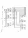
Table of Contents
v through vii/viii
August, 1987
Preface
lX
August, 1987
Section 1
1-1 through 1-4
August, 1987
Section 2
2-1 through 2-2
August, 1987
Section 3
3-1 through 3-20
August, 1987
Section 4
4-1 through 4-6
August, 1987
Section 5
5-1 through 5-2
August, 1987
Section 6
6-1 through 6-6
August, 1987
Section 7
7-1 through 7-12
August, 1987
Appendix A
A-I through A-6
August, 1987
iii/iv
M8155A
TABLE OF <nll'ENI'S
Page
1.1
1.2
1.3
~neral
PCBt\
••••••••••••••• ~ ••••••••••••••••.•.•••••••••••• •• 1-1
~scription •••••••••••••••••••••••••••••••••••••• -•• 1-1
S~if ications •••••••••••••••••••••••••••••••••••••••••• 1-1
SECTICE 2
2.1
2.2
2.3
~neral
•••••••••••••••• "•••••••••••••••••••••••••••••••• • 2-1
Unpacking/Packing Instructions •••••••••••••••••••••••••• 2-1
O{::erator Interface •••••••••••••••••••••••••••••••••••••• 2-1
SECTICE 3
3.1
3.23.2.1
3.2.1.1
3.2.1.2
3.2.1.3
3.2.1.4
3.2.2
3.2.2.1
3.2.2.2
3.2.3
3.2.3.1
3.2.3.2
3.2.4
3.2.4.1
3.2.4.2
3.2.4.3
3.3
3.3.1
3.3.2
3.3.3
3.3.4
3.3.5
3.3.6
3.4
3;4.1
3.4.2
3.4.2.1
3.4.2.2
3.4.3
3.4.3.1
3.4.3.2
3.4.4
3.4.5
~neral
••••••••••••••••••••••••••••••••••••••.••••••••• • 3-1
System I/O Interface •••••••••••••• • • • • • • • • • • • • • • • • • • • ••• 3-1
I/O Protocol Phases ••••••••••• • • • • • • • • • • • • • • • • • • • • •• 3-1
Data Packet Preparation ••••••••••••••••••••••••• 3-3
Command Block Preparation ••••••••••••••••••••••• 3-3
Corrrnand Execution ••••••••••• ................... . 3-4
Conmand Tennination •••••• • • • • • • • • • • • • • • • • • • • • • • .3-6
Interrupt Structure ••••• • • • • • • • • • • • • • • • • • • • • • • • • • • • .3-6
Z80A Interrupts ••••• • • • • • • • • • • • • • • • • • • • • • • • • • • • .3-6
System Interrupts ••••••••••••••••••••••••••••••• 3-6
Serial Communications Channels ••••••••••••••••••• ••• 3-7
~s~ge i?OI1nlElt ••••••••••••••••••••••••••••••• ••• 3-7
Signal I.<>a.ding •••••••••••••••••••••••••••••••••• 3-8
4-way Asynchronous Protocol ••••••••••••••••••••••••• 3-8
Data Line i?OI1nlElt ••••••••••• • • • • • • • • • • • • • • • • • •••• 3-8
Buffer i?low Control ~thods ••••••••••••••••• •••• 3-9
RS-232C Protocol Used by the 4-way ••••••••••• ••• 3-9
4-way Initialization •••••••••••••••••••••••••••••••••••• 3-11
Initialization Criteria ••••••••••••••••••••••••••••• 3-11
ROO Checkstnn ..•..................................... 3-11
~.ry
Test ......................................... 3-11
sec l.A:::x:>p Test ....................................... 3-11
Error Re]?C>rting ••••••••••••••••••••••••••••••••••••• 3-12
Reset Routine ••••••••••••••••••••••••••••••••••••••• 3-12
~tailed Hardware ~scription ••••••••••••••••••••••••••• 3-13
r:t1A Interface Circuits •••••••••••••••••••••••••••••• 3-13
Communications Interface Circuits ••••••••••••••••••• 3-14
Serial Communications Controllers (Sces) ••• ••••• 3-14
SCC Interrupt Acknowledge •••••••••••••••••• ••••• 3-14
Central Processor Logic ••••••••••••••••••••••••••• • .3-14
Read/Write System Memory •••••••••••••••••••••• • .3-14
Read Only Merrory (RCM) • • • • • • • • • • • • • • • • • • • • • • • • • .3-15
Read/Write Registers ••••••••••••••••••••••••••• ••••• 3-15
:Ba.ud Rate Progranming •••••••••••••••••••••••••• ••••• 3-17
v
M8155A
TABLE OF <XNrENrS (cont' d)
Page
FONC.rICtiAL DESCRIPl'ICfi (cont' d)
3.4.6
3.4.7
3.4.8
4.1
4.2
4.3
4.3.1
4.3.2
4.4
4.4.1
4.4.2
4.4.3
4.4.4
4.4
status Registers •••••••••••••••••••••••••••••••••••• 3-17
Instruction Register •••••••••••••••••••••••••••••••• 3-18
Clock Circuitry •••••••••••••• " •••••••••••••••••••••• 3-19
Preventive t1a.intenance."••••••••••••••••••••••••••••••••• 4-1
Corrective t1a.intenance •••••••••••••••••••••••••••••••••• 4-1
Power-Up Initialization And Self Test ••••••••••••••••••• 4-1
Power-Up or Hard Reset Self-Tests ••••••••••••••••••• 4-1
Soft Reset Self-Test •••••••••••••••••••••••••••••••• 4-2
Four-way Diagnostics •••••••••••••••••••••••••••••••••••• 4-2
System Power-Dn Self-Tests •••••••••••••••••••••••••• 4-2
Four-Way Logic Test (~y) •••••••••••••••••••••••••• 4-3
Four-way Function Select Test (FWFS) •••••••••••••••• 4-3
System Interaction Test (SIT) ••••••••••••••••••••••• 4-3
Hardware Configuration •••••••••••••••••••••••••••••••••• 4-3
ILLUSTRATED PARI'S LIST
6.1
Introduction •••••••••••••••••••••••••••••••••••••••••••• 6-1
IOOIC DIAGRAM
7.1
Introduction •••••••••••••••••••••••••••••••••••••••••••• 7-1
APPmDIX A
LIST OF ImIC DIAGRAM
M8155A
Vl.
~CS
LIST OF ILLUSTRATIOOS
Figure
1-1
1-2
3-1
6-1
7-1
Page
4-Way Controller PCBA - Part No. 903390 ••••••••• ~ ••••••• x
Location of Major Components on PCBA •••••••••••••••••••• 1-2
4-way Controller Functional Block Diagram ••••••••••••••• 3-2
4-way Controller PCsA (P/N 903390) •••••••••••••••••••••• 6-2
4-way Controller PCBA - Logic Diagram ••••••••••••••••••• 7-1
LIST OF TABT.ES
Table
1-1
3-1
3-2
3-3
3-4
6-1
Page
4-way Controller Specifications ••••••••••••••••••••••••• 1-1
Asynchronous Communications Connector Data •••••••••••••• 3-8
RS-232C Signals Used by the 4-Way ••••••••••••••••••••••• 3-10
Functions Assigned to Each Read/Write Register •••••••••• 3-16
Time Constant Divisors Required for
Various Bctud Rates •••••••••••••••••••••••••••••••••••• 3-17
4-Way Controller PCBA Parts List •••••••••••••••••••••••• 6-3
vii/viii
M8155A
This manual provides servlce information for the 4-way Controller Printed Circuit Board Assembly. The information is presented as an aid for field service
personnel, and supports the installation, operation, and maintenance of the
PCBA.
The major topics covered in this manual are:.
Section 1
Section 2
Section 3
Section 4
Section 5
Section 6
Section 7
Appendix A
Introduction
Installation
Functional Description
Maintenance
Removal/Replacement
Illustrated Parts List
Logic Diagrams
List of Logic Diagram Mnemonics
This equipoent generates, uses, and can radiate radio frequency
energy and i f not installed and used in accordance with the instruction manual, may cause interference to radio CCIlI'IIlDications.
It has been tested and found to cutply with the limits for Class A
CCIIplting devices pn-suant to SUbpart J of Part 15 of FCC Rules,
which are designed to provide reasonable protection against such
interference when operated in a cumterCial enviromelt. ~ration
of this equipoent in a residential area is likely to calJse interference in which case the user at his own expense will be required
to take whatever measures that may be required to correct the interference.
.
The use of shielded I/O cables is required when connecting writ to
any and all optional peripheral or host devices. Failure to do so
may violate FCC rules.
1.X
M8155A
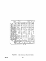
Figure 1-1.
M8155A
4--way Controller PCR2\ - Part No. 903390
x
1.1 GENERAL
The 4-Way Controller PCBA, part number 903390, Figure 1-1, provides the means
by which a MAl 2000/3000 computer system communicates with up to four RS-232C
asynchronous data I ines to which Data Corrmunications Equipnent (DeE) can be
connected. Each Serial Communications Channel (SCC) has software programnable
character formats and baud rates.
1.2
PCBA DESCRIPl'IOO
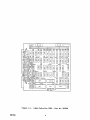
The 4-Way PCBA is designed for horizontal mounting in the 2000/3000 housing.
All components are mounted on one side of the board and are hard wired and
soldered except for the mrrcroprocessor, controller, controller firmware, input
RAM and driver chips, which are socketed. Connections to the DeE equipnent
being serviced are made via four metal-faced 9-pin D-type female connectors on
one side of the PCBA. In addition to the electronic and electric components,
the PCBA also contains a lO-position DIP switch for establishing bus contention priorities and a green LED for indicating Initialization/PASS status (ON)
or FAIL status (OFF). See Figure 1-2.
1.3
SPECIFICATIOOS
Table 1-1.
~ating
4-way Controller Specifications
Environnent
Temperature:
Humidity:
20% to 80% relative humidity with a maximum gradient of 10%
per hour, non-condensing.
Pressure:
Altitude equivalent 10,000 feet, maxlffium
storage and Shiwing Environnent
Temperature:
-15° to 65°C (storage)
-40° to 71°C (shipping)
Humidity:
10% to 90% relative humidity with no condensation permitted.
Pressure:
Altitude equivalent 40,000 feet, maximum
1-1
-47° to 150°F
-72° to 160°F
M8155A
Figure 1-2.
M8155A
Location of Major CalPlnents on PCB1\
1-2
1-3
M8155A
M8155A
1-4
INSTALIATION
2.1
GmFlW..
This section contains unpacking/packing instructions and installation requlrements for the 4-way Controller.
The 4-Way is shipped in an anti-static bag, inserted between two layers of
styrofoam and sealed in a cardboard shipping carton. Unpack the 4-Way as
follows:
1.
Prior to accepting the package from the carrier, inspect the shi~
ping carton for signs of external damage. Any indication of external damage must be noted on the carriers's shipping form and
reported immediately to the MBF Sales Office.
When unpacking the PCBA, set aside the
packing materials and shipping carton for
use if it should become necessary to
reship. The PCBA is ESD sensitive.
Proper handling procedures should be used.
2.3
2.
With the PCBA shipping carton in its upright position, open the
carton and carefully remove the PCBA.
3.
Unwrap the PCBA and inspect it for signs of shipping damage.
mediately report any damage to the MBF Sales Office.
Im-
OPmA'Im INTERFACE
There is no operator interface to the 4-way Controller.
2-1
M8155A
M8155A
2-2
SEX!1'ICfi 3
3.1
GEmlW,
This section contains a functional description of the 4-Way Controller on
three levels: a general block diagram description, a discussion of the system
1/0 interface characteristics, and a detailed discussion of the 4-Way Controller circuits.
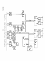
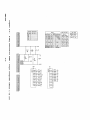
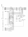
Figure 3-1 is a functional block diagram of the 4~y, showing the relationship among the several functional areas of the controller. The ZaOA-CPU
is the central processing element in the 4-Way Controller. (A detailed discussion of the ZaOA-CPU is contained in the Zilog "ZaOA-CPU Technical Manual",
which is not furnished.)
The Z-aOA-CPU provides data handling assistance to the Central Microprocessor
Board (eM) in the DTU and controls overall 4-Way operations. When service is
required to receive characters or other special conditions, the 4-Way issues
an interrupt to the CMB. The CMB prep3res a data packet of between 1 and 512
bytes in length, creates a Command Block containing the location of the packet
and places the information in a preprogrammed location in DTU memory. The 4Way fetches the data from CMB Inem)ry one word at a time and sends an interrupt
upon completion of the transfer.
3.2
SYSTEM I/O IN1'ERFACE
The System Software Interface consists of activation paths which allow the DTU
software to communicate with the four SCCs (Serial Communications Channels)
via the ZaOA-CPU and response (interrupt) paths which allow the SCCs to interrupt the CPU in the DTU .via the zaOA-CPU.
3.2.1
I/O Protocol Phases
The softwarelhardware protocol consists of from one to four separate phases
which are described in the paragraphs indicated, as follows:
o
a
o
o
Data Packet Preparation (paragraph 3.2.1.1)
Command Block Preparation (paragraph 3.2.1.2)
Command Execution (paragraph 3.2.1.3)
Command Termination (paragraph 3.2.1.4)
3-1
M8155A
i
I-'
U'I
~
I'Zj
j'
~8-D1~
B
k
M5B DATA
5240.
4
B
MSB
DATA
~l5374 v--,
: • 4 .I"vl I
8530
SCC-l
W
I
I-'
•
I
~~.., . . .t------~--__==:_:::J ~
~H"
w
I
IV
COMMAND
REGISTER
LS374
a..........
DATA
&
8530
SCC-2 A
,
>I
Z80A
CPUDATAK
----'
:
2016
2K x 8
RAM
BOARD
~
0
Vt
CONTROL
~ S240
~
~
~..
~~g~5~s
--"'-""r-----s
BUS
CONT
LOGIC
INTRPT
LOGIC
A
...
P2
I
/
/16
/ADDRESS
v
DATA
ADR
2K x 8
PROM
RS232
DRIVERS
UREC~IVERS
DATA
B
"--'
Ie--
P3
~~~~----------~I
~
.....
Cd
.....
--
~
RECRIVB14-t- ERS
I
Ie
I¢
LS273
[....
~
I
..
~ DATA
RS232
DRIVERS
BOARD
STATUS
:
~
s·
;
TRANSMIT
STATUS
~
8/
A~
PI
ADR
P4
Data Packet Preparation
3.2.1.1
A Data Packet (DP) must be established by the host CPU before any data transmission can be accomplished. The DP can be between 1 and 512 bytes in length
and is organized as follows: The MSB of each word is sent first, followed by
the LSB. The DP starting address is then placed in the preassigned Corrtnand
Block for the specified fX)rt. The starting address must be placed on a word
boundary, since the 4-Way is unable to address odd-byte locations.
3.2.1.2
Cbmmand Block Preparation
The Command Block is the mechanism that the host CMB uses to inform the 4-Way
what corrtnand is to be performed, where the DP is, and how large the DP is.
The following is the format required for each Corrtnand Block memory area:
(HJ
AIDmSS
<nll'ENrS
Base Address
Add + 2
Add + 4
Add + 6
Add + 8
Add + 10
Add + 12
Add + 14
Add + 16
Add + 18
Add + 20
Add + 22
Add + 24
Add + 26
Add + 28
Add + 30
Add + 32
Add + 34
Add + 36
Add + 38
Command Word, Port A
Data Byte Count, Port A
Data Packet Address, MSB,
Data Packet Address, LSB,
Transfer status (4-Way to
Corrmand Word, Port B
Data Byte Count, Port B
Data Packet Address, MSB,
Data Packet Address, LSB,
Transfer status (4-Way to
Corrtnand Word, Port C
Data Byte Count, Port C
Data Packet Address, MSB,
Data Packet Address, LSB,
Transfer status (4-Way to
Coomand 'Word, Port D
Data Byte Count, Port D
Data Packet Address, MSB,
Data Packet Address, LSB,
Transfer status (4-Way to
Port A
Port A
CMB), Port A
PQrt B
Port B
CMB), Port B
Port C
Port C
CMB), Port C
Port D
Port D
CMB) , Port D
SAMPLE <XHWID BI.DCK
15
0
0
0
0
14
10
12
11
09
13
0
0
0
0
0
0
0
0
0
0
0
0
0
0
0
0
0
0
MID Data Packet Address
0
0
0
0
o: 0
I
I
I
I
I
I
I
I
I
I
01
03
02
05
04
08
07
06
0
Corrrnand
0
0
0
0
0
Data Packet Byte Count
MSB Data Packet Address
0
LSB Data Packet Address
Command
status (from 4-Way)
0
I
I
I
I
I
I
I
I
I
I
I
I
I
I
I
I
The CMB activates the 4-Way to execute a corrtnand by outputting the appropriate
bit to the Instruction Register (Port Address D(x)AOOOH)
3-3
M8155A
All addresses sent to the 4-way must be on
word boundaries; therefore, the actual 4way starting address has been shifted one
bit to the right. Example: To reach address 0640AH, the 4-way must recei ve
OlAOSH.
3.2.1.3 Cbmmand Execution
Receipt in the Instruction Register of a valid flag from the CMB causes the 4way to read the identified Command Block and execute the command as specified
by the Command Word. The current command can be overridden or terminated
under special conditions, as follows:
o
The Port Reset/X-oN Reset command will clear all buffers and pointers in
a port which is "hung up," without affecting the other ports. If an XOFF condition exists in the same port, the Reset command will 1ssue an
X-oN to the port and continue without loss of data.
o
If a Command Word is not recognized by the 4-Way, it will transmit an
Illegal Comnand code (OFF H) to the status byte of- the Command Block
being serviced, causing a termination o~ the command.
The following are the commands issued to the 4-Way in the Command Block:
CDDE (Hex)
00
01
02
03
04
05
06
07
08
09
OA
OB-FF
OPEBATIOO
mJHN[C
Not Used *
Configure
Data Transfer
status
Load Default Parameters
Load X~N Value
Load X~FF Value
Single Byte Transfer
X~N Enable/Disable
Hard Flow Enable/Disable
7 Bit/8 Bit
Not Used *
(CONF)
(Dr)
(STS)
(IDDEF)
(IDXON)
(IDXOF)
(SINGL)
(ENXON)
(FLOW)
(EIGT)
* - Illegal Command status 1S returned.
o
Cbmmand Configuration - For each register to be changed, the Data Packet
(DP) must specify the register number first, followed by the new command.
M8155A
3-4
o
Data Transfer - UfX)n rece1v1ng the Command Block, the ZSOA-CPU causes
the packet to be transferred a word at a time and simultaneously programs the selected SCC in the proper sequence to handle the serial
transmission of data to the neE being serviced. The Z80A-CPU then 1Ssues an interrupt to the CMB upon completion (Command Executed
Interrupt) •
o
status - The status Command is the only command that allows the 4-Way to
write to system memory; therefore, the CMB reserves 8 consecutive word
memory locations prior to issuing the status Command. UfX)n receiving
the status Command, the 4-Way sends (via DMA) all the data in the Read
Registers of the specified SCC. The Corrmand Block byte count is ignored
while the 4-Way status information is written into CMB memory using the
lower 8 data lines (the UJ;.Per lines· are indeterminate). The 8 lines
contain the following information:
RmISrER ID.
o
Add
+
0
RRO
Add
Add
Add
Add
Add
+
+
+
+
+
2
4
6
8
10
RR1
RR2
RR3
RR10
RR12
Add
+
12
RR13
Add + 14
RR15
DESCRIPrION
Transmit/Receive Buffer status; External
status
Special Receive status
Unrocxiified Interrupt Vector
Interrupt Pending Bits
Miscellaneous status
Lower Byte of Baud Rate Generator Time
Constant
Upper Byte of Baud Rate Generator Time
Constant
External/Status Interrupt Control Information
IDad Port Default ParaIEte.rs - This command tells the 4-Way to load the
default parameters to the SCC fX)rt being addressed: 9600 Baud, 1 start
Bit, 1 stop Bit, Odd Parity.
o
!Dad
x-on Value - This conmand allows the
CMB to alter, via software,
the ASCII character which is used as the X-oN character for each fX)rt.
The default values of 011H and 091H are assigned to all fX)rts of the 4Way during initial Reset. The new value is placed in the Command Block
in place of the Byte Count (lower 8 bits). An eight-bit alternate form
of the X-oN value can also be used.
o
IDad X-off Value - This command allows the CMB to alter, V1a software,
the ASCII character which is used as the X-oFF character for each fX)rt.
The default values of 013H and 093H are assigned to all fX)rts of the 4Way during initial Reset. The new value is placed in the Command Block
in place of the Byte Count (lower 8 bits). An eight-bit alternate form
of the X-oFF value can also be used.
o
Single Byte Transfer - This conmand allows the CMB to transfer a single
byte of data from the CMB to the specified fX)rt. The data to be transferred is placed in the Command Block in place of the Byte Count (lower
8 bits). No DP address is required. A Command Executed Interrupt is
sent ufX)n completion of the transfer.
3-5
M8155A
o
X-aN Enable/Disable - This command toggles the DTR and CTS lines to
enable or disable the hardware flow controls. Flow control is enabled
when the Byte Count of the Command Block equals 1 (OlH), and is disabled
by any otQer Byte Count value. The default setting is Hardware Flow
Control Enabled.
o
7-Bit/8-Bit Data - This command tells the 4-way whether it is handling
7-bit or 8-bit data. If 7-bit data is selected, the eighth bit is
stripped off by the CMB. If 8-bit data is selected, all data is passed
along to the 4-way with no conditioning. A Byte Count value of 1 (OlH)
in the Command Block configures the specified 4-way receive port for 7
bits; any other value configures the port for 8 bits. The default setting is for 7 bits.
3.2.1.4 Oommand Termination
After each command is received, the 4-way firrrMare writes the status in the
awropriate Coomand Block to infonn the CMB that the command has been executed
( 081H) or the 4-way did not understand the command (083H). If a Bus Error occurs during any of the DMAs, the 4-way terminates the current operation and
places the value 083H in the status Byte of the awropriate Command Block.
3.2.2
Interrupt structure
3.2.2.1
Z80A Interrups
SCCs are programmed to interrupt the Z80A when they need service. An interrupt vector, originating the Read/Write registers, points to a transmit or
receive service routine or to an external/status condition. As many as 17
different interrupt routines (four per channel and one board level) can be
enabled under program control. Channel A has a higher priority than Channel
B, C or D; Channel B has a higher priority than ehannel C or D, and so on.
Within each channel, the priority levels are: receive, transmit, external/
status, respectively.
The see interrupt ~ignals share a cammon level and are OR'ed to a common interrupt signal. The first request for service is serviced first; the other
secs are disabled. Simultaneous requests are handled on the basis of an A-Bc-o priority. When the command has been executed, or is detennined to be unexecutable, the Z80A polls the SCCs for an empty FIFO transmit buffer and
loads it. The 4-way then sends the CMB an awropriate interrupt.
3.2.2.2
System
Interrups
When the CMB receives the transmitted interrupt from the 4-way, it responds
with an Interrupt Acknowledge, causing the 4-Way to transmit an Interrupt Vector containing the status information for the selected channel. The Interrupt
Vector consists of a Base Address followed by three Additional Addresses,
structured as follows:
M8155A
3-6
3.2.3
Base Address
Add + 1
Add + 2
Add + 3
Ch
Ch
Ch
Ch
A External/Status Change
A Receive Character Available
A Special Receive Condition
A Command Executed
Add
Add
Add
Add
+
+
+
+
7
Ch
Ch
Ch
Ch
B External/Status Change
B Receive Character Available
B Special Receive Condition
B Command Executed
Add
Add
Add
Add
+
+
+
+
a
9
10
11
Ch
Ch
Ch
Ch
C
C
C
C
Add + 12
Add + 13
Add + 14
Add + 15
Ch
Ch
Ch
Ch
D External/Status Change
D Receive Character Available
D Special Receive Condition
D Command Executed
4
5
6
External/Status Change
Receive Character Available
Special Receive Condition
Command Executed
Serial Cammri.cations Channels
The four asynchronous communications channels are serviced by two USARTs which
support only primary RS-232C signals. Secondary signals and the time options
of the RS-232C are not supported. Communication may be single channel fullduplex or single channel half-duplex.
3.2.3.1
Message Format
A typical 7-bit asynchronous message format consists of one start bit, seven
data bits, one parity bit and one or two stop bits. (An a-bit message format
may also be called for.) The following discussion of the characteristics of
the message format assumes the active signal condition to be the mark state
(-3 to -25 volts):
o
start Bit - Its transition to mark state notifies the 4-Way receiver of
an incoming message; also initiates a clock circuit to provide latching
pulses during the expected data bit intervals.
o
Data Bits - Data bits have standard TIL values: 0.0 to +0.4 VOC equals
logic low; +2.4 VOC to Vcc equals logic high.
o
Parity Bit - Provided for error checking, it rests in the quiescent (0)
state or the mark state (1), depending upon whether the accumulated l's
in the data bits are odd or even. The parity bit is calculated in both
the sender and receiver and the results for each data word are compared
to ensure that the actual and expected data-bit values match.
3-7
M8155A
o
stqp Bit(s) - The stop bit momentarily transits from its normal high
state to its mark state at the end of each message unit, causing the
receiving circuits to be reset in preparation for the next start bit.
During reception, the start and stop bits are stripped away, leaving
only the working data for CPU interaction.
3.2.3.2 Signal Loading
Each communications channel (gate) uses one 1489 line receiver for input loading and one 1488 line driver for output. The- four channels corrmunicate with
the connected equipment via a 9-pin connector which has the characteristics
specified in Table 3-1. An open DSR or nco pin is biased to be in the active
(mark) state so that communication will not be blocked by non-~lemented Slgnals. (The biasing can be rennved or Irodified by manipulating the jumper
block for the port in accordance with the information shown in the logic
diagram in Section 7 of this manual.) The device type data suppl ied by the
CMB software informs the 4-Way what equipnent is connected, and thus what
protocol is needed; the 4-Way masks out the undesired signals when reading
from the see status Registers.
Table 3-1. Asynchronous camunication Connector Data
PIN t
1
2
3
SIGNAL
mNJ[~/mIVER
RF.Ml\RKS
TxD
RxD
RTS
crs
DSR
1488
1489
1488
1489
1489
(Driver)
(Receiver)
(Driver)
(Receiver)
(Receiver)
6
7
nco
1489 (Receiver)
Transmitted Data
Received Data
Request to Send
Clear to Send
Data Set Ready
Signal Ground
Data Carrier Detect
8
9
JJrR
1488 (Driver)
Data Terminal Ready
4
5
SG
3.2.4 4-way Asynchronous Protocol
This discussion of 4-Way asynchronous protocol assumes that the data sender
(or data sourcer) is called Data Set, and the data receiver (or data sink) is
called Data Terminal.
3.2.4.1 Data Line Format
character or message unit is defined by a start bit and one or two stop
bits. Traditionally, one stop bit is used when the baud rate is higher than
110 baud; two stop bits are used when the baud rate is lower than 150 baud.
One-and-a-half stop bits are also possible in some terminals. Character
length can be programmed from 5 to 8 bits, excluding the parity bit, and
parity can be programmed as odd, even or no parity.
A
M8155A
3-8
3.2.4.2
Buffer Flow Control Methods
If the Data Tenninal has slower throughput than its input, the Data Terminal
buffer may become full. One of three flow control methods is used to prevent
buffer overflow, as follows:
o
o
o
X~/X~FF
Protocol
Data Tenninal Ready Control
Data Set Ready Control
X~/X-{)FF
Protocol - Two otherwise unused ASCII codes are embedded in the
output message by the Data Tenninal to announce the full/empty condition of
its receive buffer. The codes are software configurable for each fX)rt, but
have default values of 011H and 091H for X-GN, and 013H and 093H for X-GFF.
The CMB can also send an X~N to the 4-Way by issuing a port Reset command
while the fX)rt is in an X-GFF condition. When under the control of the Data
Terminal, the protocol gives the following instructions to the CMB: 1) When
X-GFF is received, halt transmission; 2) Wait for X~N code; 3) Continue
transmission until X~FF code is received.
Data Tenni.nal Ready Control - When on-line to the CMB, the Data Tenninal can
control the input to its buffer by toggling the Data Terminal Ready (DTR) line
as follows: DTR in the mark state means buffer is full and transmission is to
be hal ted; otherwise, continue transmission.
Data Set Ready Control - This method is used when the Data Tenninal speed ex-
ceeds that of the data source, or when the tenninal is unable to receive any
character within certain time intervals after a carriage return or line feed
is received. In this event, the Data Set Ready (DSR) line is held in a mark
state and the Data Set controls the transmission speed. If necessary, null
codes are inserted between characters to slow the transmission speed. If this
method is used, the data sink software should reject the null codes before
storing the received data.
3.2.4.3 RS-232C Protocol Used
h¥
the
4~y
Table 3-2 identifies all the standard RS-232C signals that are available;
those that are involved in 4-Way protocol are discussed in the paragraphs that
follow.
•
3-9
M8155A
Table 3-2.
RS-232C Signals used by the
4~y
st.aOOard RS-232C InplE!DeDtation
M
AS
CE
CD
CC
EA
DA
DB
DD
CA
CB
CF
CG
CH
CI
SEA
SBB
SCB
SCF
Protective Ground
Signal Ground
Ring Indicator
Data Tenninal Ready
Data Set Ready
Transmitted Data
Transmitter Signal Element Timing
(DTE Source)
Transmitter Signal Element Timing
(DCE Source)
Receiver Signal Element Timing
Request to Send
Clear to Send
Data Carrier Detect
Signal Quality Detector
Data Signal Rate Selector (IJrE Source)
Data Signal Rate Selector (DCE Source)
Secondary Transmitted Data
Secondary Received Data
Secondary Clear to Send
Secondary Received Line Signal Detector
4-way
NO
YES
NO
YES
YES
YES
NO
NO
NO
YES
YES
YES
NO
NO
NO
NO
NO
NO
NO
Transmitted Data (TXD) - Signals on this circuit are generated by the IJrE and
are transferred to the 4-Way USART for transmission to the host. The signal
is held in the marking state during intervals between characters and at all
times when no data is being transmitted.
Received Data (RxD) - Signals on this circuit are generated by the host in
re5pJnse to data signals received from the 4-way USART. This line is held in
the marking state during intervals between characters and at all times when no
data is being received (DCD off).
a half-duplex channel, the Received Data line is held in the marking state
when RTS is asserted and for a brief interval following the ON (~sserted) to
OFF transition of RTS to allow transmission to be completed.
On
Data carrier Detect UXD) - Data Carrier Detect is generated by the host to
qualify the Received Data line signal. Based on the protocol, if Auto Enable
r.bde is not selected, data can still be received when DCD is in the mark state
(FALSE). The 4-Way software decides whether data is acceptable or not.
to SeOO (RrS)/Clear to Send (c.rs) - Request to Send (RTS) and Clear to
Send (CTS) are meaningful when a half-duplex Irodem is involved. RTS requests
a communication channel from the host; CTS from the host acknowledges the request. In half-duplex communication, the 4-way must send RTS and the host acknowledge with CTS before each character can be transmitted. The Transmitter
Shift Register Empty signal in the SCC status Register is used to ensure that
the last stop bit is fully transmitted before RTS is released.
Request
M8155A
3-10
Data Set Ready (£Sl) ...:. Data Set Ready is sent to the 4-way by the rrodem to in-
dicate its on-line condition. DSR is also frequently used to indicate that a
connected DTE element is in the proper condition to receive data (on-line,
with receiving buffer not yet full). DSR is placed at the External Sync pin
of the SCC and can generate an External status Interrupt on any transition.
The DSR bits can also be read from the 4-Way status Register at any time.
Data Temri.nal Ready (UlIU - Data Terminal Ready is set to its marking state
(FALSE) to indicate that the 4-Way is on-line and ready to receive data
(receive buffer not yet full).
3.3
4-wAY INITIALIZATIOO
The 4~y is initialized by a Master Reset or a Power On Reset (POR). The
condition causes the 4-way to initiate a Self-Test routine during which
several power-on (or reset) tests are performed, as discussed in the paragraphs that follow. Successful completion of the Self-Tests is signalled by
illuminating the green LED light on the PCBA.
3.3.1
Initialization Criteria
a cold-start initialization, the LED is OFF. It is turned ON if and when
the Self-Tests are successful. On a warm-start initialization (Software Reset
Command), the LED is ON and is momentarily toggled OFF as an indication that
all hardware has been initialized. If the LED remains OFF, a Fatal Error has
occurred and the 4~y is inoperable and remains so until the Fatal Error is
fixed.
On
3.3.2 IDt Checkstn
As the 4-way enters the PROM Checksum routine, the LED is set to OFF. All
PRCM locations are added together in rrodulo 256 and compared to' an expected
sum stored in the PROM. If the checksum fails, a Fatal Error Code is generated.
3.3.3 Memory Test
A series of simple data patterns are run through 4-way memory to verify the
ability of each memory cell to hold both ones and zeroes.
3.3.4
sec Wop
Test
All four channels are loop-tested in asynchronous mode to verify interrupt,
data continuity, and basic timing. During the test, the serial lines are disabled to ensure that devices on the line are not affected by the testing. All
parallel-to-serial logic on the 4-Way is tested except the driver/- receivers
of the serial interface.
3-11
M8155A
3.3.5
Error Reporting
During Self-Test, the Self-Test bit in the Transmit Status Register is set and
remains set for the duration of the tests. Should a test fail, an error code
is placed in the Receive Data Register to indicate which test failed. If the
test is critical to the operation of the 4-way, the Fatal Error bit is set and
the 4~y will go off-line. The Error Code bits for the Receive Data Register
have the following significance when set during Self-Test mode:
Bit
Bit
Bit
Bit
Bit
Bit
Bit
Bit
O(ISB)
1
2
3
4
5
6
7
RAM Failure
Always Zero
Always Zero
Always Zero
see Port A Failure
sec Port B Failure
sec Port C Failure
SCC Port D Failure
Reset Routine
3.3.6
Upon successful completion of Self-Test (no errors), the LED is set to ON and
control is passed to the Reset routine, which proceeds as follows:
1.
The asynchronous parameters of the sec are set as follows:
bit, 7 data bits, odd parity, one stop bit, 9600 baud.
2.
Bits 2 and 3 are set in the status Register to indicate to the CMB
that the Base Interrupt Vector and the Base Command Block Address
have not been set for the 4-Way. The CMB then writes the least
significant word of the Command Block Address to the 4-way Instruction Register.
3.
The CMB monitors the BUSY flag (bit 0) of the 4-way status Register. Bit 0 is set and remains set until the Z80A has transferred
the address to memory and is ready for the next address.
4.
The CMB, upon sensing the reset of Bit 0, writes the most Slgnificant byte of the Command Block to the lower byte of the host
data bus.
5.
The process 1S repeated for the Base Interrupt Vector.
6.
The 4-Way enters the Executive Program, in which data is passed
along to the appropriate devices connected to the 4-way.
M8155A
3-12
1 start
3.4
IEl'AILED
~
DESCRIPrICE
In this section, the operating characteristics of the electronic and logical
elements of the 4-Way Controller are described 1n terms of their functional
groupings, as follows:
o
o
o
o
o
o
o
o
3.4.1
DMA Interface Circuits (paragraph 3.4.1)
Communications Interface Circuits (paragraph 3.4.2)
Central Processor Logic (paragraph }.4.3)
Read/Write Registers (paragraph 3.4.4)
Prograrrmable Baud Rate Generator (paragraph 3.4.5)
status Register (3.4.6 )
Instruction Register (paragraph 3.4.7)
Clock Circuitry (paragraph 3.4.8)
rM\ Interface Circuits
The DMA interface (see sheet 5 of the Logic Diagram) is activated when the
Z80A asserts SETBREQ-, which forces the Bus Request signal BR- onto the EBUS,
and into the DMAI/Interrupt Arbitration portion of the DMA Interface. At this
time REQ2+ is generated to activate the arbitration process. The settings of
dip switches 1 thru 6 (AFSA-l to ASSA-3) determine the priority level the 4Way will use in any DMA or Interrupt arbitration. The S157, S38 and S64 chips
determine if the arbitration levels match.
If the first stage of arbitration is correct, PG2- is set; if the second stage
of arbitration matches, MYTORN- is asserted TRUE. If AS+, IACK+ and ~CK+
are all inactive (FALSE) the DMA cycle commences with the next GO+ strobe.
Several strobes are created:
a.
!II;ACK+,
which becomes :EG\CK- (Bus Grant Acknowledge signal on
EBUS)
b.
which enables·the address drivers to place the pre-loaded
DMA address on the EBUS.
c.
START+, which creates IJtWD+ to keep the Drive
alive until the DMA cycle is completed.
I~-,
Bus
Signal OOBOS-
To terminate the DMA cycle, one of two events occur, either of which causes
the ~p- and WHOA- signals to turn off the DMA cycle: ~+ (Data Transfer
Acknow ledge) or amR+ (Bus Error).
The following are the only valid arbitration switch settings for the 4-Way:
Board
1
2
3
4
AFSAl
o
o
o
o
1
1
1
1
1
1
1
1
3-13
1
o
o
o
1
1
o
o
1
1
1
o
M8155A
3.4.2
camuni.cations Interface Circuits
3.4.2.1
Serial camuni.cati9flS Controllers
(SCCs)
All RS-232C communications are handled by the SCC chips. These chips handle
the protocol, baud rate, and characteristics of the input and output serial
. data. Refer to the Zilog 8530 Technical Manual for de~ils of the SCCs.
3.4.2.2
sec Interrupt. h::knowledge
The timing arrangements of the SCCs require that a Z80A wait state be generated to allow the scc to complete daisy chain prioritization during an Interrupt Acknowledge cycle. During an Interrupt Acknowledge cycle, ZINTACKasserts Read strobe READ- to SCCs and issues wait strobe ~- to the Z80A.
central Processor Wgic
3.4.3
The Z80A-CPU Microprocessor is the central processing element in the 4-way
Controller. The operation of the Z80A-CPU is described in full detail in the
Zilog Z80A-CPU Technical Manual (not supplied).
3.4.3.1 ReadlWrite Systan Me!oory
The Read/Write System Metoory contains interface logic to the Z80A bus, address
buffering and timing logic, and a 2K x 8 Type 6116 RAM IC. The memory 1S
divided into 9 sections, one 256-byte section for the Z80A scratchpad, four
192-byte FIFO sections for transmitted data, and four 256-byte sections for
received-data buffering. The following RAM memory map shows the starting address for each of the 9 sections:
Address
Address
Address
Address
Address
Address
Address
Address
Address
M8155A
2000H
2100H
21COH
2280H
2340B
2400H
2500B
2600B
2700H
-
Z80A Scratchpad, 256 Bytes
Channel A FIFO, 192 Bytes
Channel B FIFO, 192 Bytes
Channel C FIFO, 192 Bytes
Channel D FIFO, 192 Bytes
Channel A Receive Buffer, 256
Channel B Receive Buffer, 256
Channel C Receive Buffer, 256
Channel D Receive Buffer, 256
3-14
Bytes
Bytes
Bytes
Bytes
3.4.3.2
Read Only Mem>ry (RCM)
The 4-Way ROM consists of a Type 2764 EPROM, which provides 8k x 8 bits of
microprocessor firmware storage. The following functions are provided within
the ROM address range of OOOOH to 2000H:
Self-Test Routine - The Self-Test Routine is activated upon initial power up
or Power On Reset (POR). The ROM, RAM, SCC Channels, and Il1A logic are all
tested, and if anyone should fail, a Fatal Error is generated an~ sent to the
CMB. The 4-Way becomes inoperative and remains so until the error is corrected. If no Fatal Error is detected, 4-Way control is passed on to the
Reset function.
Reset Routine - The Reset function causes the 4-Way
routine located at address 066H. Reset initializes
configuration and then allows the CMB to initialize
Address and Interrupt Vector before passing control
to begin executing the
the SCCs with a default
the 4-way Command Block
to the Executive Routine.
Executive Routine - This resident program is stored 1n an 8K x 8 EPROM and 2K
x 8 of RAM to provide initial 4-way control after a Reset in the following
manner:
o
The Executive monitors the Instruction Register and reports to the OMS
whether a Data Packet has been prepared for transmission.
o
The Executive handles all data transfers between the 4-way and the OMS
and between the 4-way and each of the four asynchronous ports.
3.4.4 ReadlWrite Registers
The center of data activity in the 4-Way revolves around the internal Read/
Write Registers, the programming of which provides the SCC with a functional
"personality." This programming is controlled from the Z80A which uses the 8bit address bus to control an address decoder. Through these decoders the
register values can be assigned before or during program sequencing to
determine how each SCC will establish a given communication protocol. All
communication modes are established by the bit values of the Write Registers.
As data is received or transmitted, the bit values of the Read Register
change. These changed values may promote software action or internal hardware
action which result in further Read Register changes.
The register set for each channel includes 16 Write Registers and 9 Read Registers. Ten Write Registers are used for control, two for sync character generation, and two for baud rate generation. The two remaining Write Registers
are shared by both channels: one for processing Interrupt Vectors and one as
Master Interrupt Control. Of the nine Read Registers, four indicate status
functions, two are used by the Baud Rate Generator, one is for the Interrupt
Vector, one for the Receive Buffer, and one is for reading the Interrupt Pending bits. The assigned functions for each Read/Write Register are listed and
described in Table 3-3.
3-15
M8155A
Table 3-3.
Functions Assigned to Each ReadlWrite Register
RFAD REX;ISrER FDNCrIONS
RRO
Transmit/receive buffer
status; external status
WRO
Command Register pointers;
CRC initialization; commands
for various modes
RR1
Special receive condition
status; error conditions
WR1
Interrupt conditions; data
transfer modes
RR2
Modified (Channel B only)
Interrupt Vector; unmodified vector (Channel A
only)
WR2
Interrupt Vector (access
through either channel)
RR3
Interrupt Pending bits
(Channel A only)
WR3
Receive/control parameters;
No. bits/character
WR4
Transmit/receive miscellaneous
parameters and modes
WR5
Transmit parameters and control
WR6
Sync character or SDLC address
field (1st byte)
WR7
Sync character or SDLC flag
(2nd byte)
WR8
Transmit buffer
WR9
Master Interrupt Control and
Reset (accessed thru either
channel)
WR10
Miscellaneous transmitter/
receiver control bits
WR11
Clock mode control
RR8
RR10
Receive buffer
Miscellaneous status
parameters
RR12
Lower byte of baud rate
generator time constant
WR12
Lower byte of baud rate
generator time constant
RR13
Upper byte of baud rate
generator time constant
WR13
Upper byte of baud rate
generator time constant
WR14
Miscellaneous control bits
WR15
External/status interrupt
control information
RR15
M8155A
External/status interrupt control information
3-16
3.4.5
Bam Rate
Progranming
Each channel in the 4-Way contains a Baud Rate Generator which consists of a
16-bit down counter (two 8-bit time-constant registers), and a square-wave
outplt flip flop. The time constant can be changed at any time to program a
new baud rate, under the following conditions:
.
o
The new value will take effect only up:m the next load of the counter.
o
No attempt is made to synchronize the new time constant with the clock
used to drive the generator.
o
When the time constant is to be changed, the Baud Rate Generator is
stopped by writing an enable bit inWR14 to ensure that the correct time
constant is loaded.
Table 3-4 shows the divisors needed to produce the time constant needed to
generate a x16 clock for the various baud rates. The divisor is calculated ln
accordance with the formula:
Divisor = [1/(2 * BR* 1/Freq)] - 2, where
Freq = 3.6864 MHz.
Table 3-4.
Time Constant Divisors Required for Various
DESIRED
B.2\UD
RATE
3.4.6
DIVI&Jl
Bam Rates
DESIRED VS AcruAL
PmcENl' ERRCE OF
DIFFERENCE
RBJUIRED F<E
X16 CIDCK
50
75
150
300
600
1200
1800
2400
3600
4800
7200
9600
19200
38400
2.302
1,534
766
382
190
94
62
46
30
22
14
10
8FE
5FE
2FE
17E
BE
5E
3E
2E
1E
16
4
1
4
1
Percent Error
= 100 * [(Desired BR - Actual BR)/Desired BR]
E
A
status Register
The status Register contains information on the readiness of the· 4-Way to
receive data, which is sent to the OMS in response to the Transmit status Register command, via the lower 8 bits of the 4-Way to CMB Data Bus. The CMB interprets the status Register bit pattern differently, depending upon whether
Self-Test Bit 1 is set (Self-Test Mode) or not set (Normal Mode).
3-17
M8155A
The significance of the bits (when set) for Normal Mode and Self-Test Mode are
as follows:
Normal M:xie
Bit
Bit
Bit
Bit
Bit
Bit
Bit
Bit
Self-Test
Bit
Bit
Bit
Bit
Bit
Bit
Bit
Bit
0 (LSB)
1
2
3
4
5
6
7 (MSB)
Busy (4-Way not ready)
Self-Test off (must be zero)
Conmand Block Address not received
Base Interrupt Vector not received
DSR Channel A (negative TRUE)
DSR Channel B (negative TRUE)
DSR Channel C (negative TRUE)
DSR Channel D (negative TRUE)
~
0 (LSB)
1
2
3
4
5
6
7 (MSB)
Fatal Error (4-Way inoperative)
Self-Test in progress (must be set)
RCM Failure (Fatal Error)
DMA Bus Failure (Fatal Error)
DSR Channel A (negative TRUE)
DSR Channel B (negative TRUE)
DSR Channel C (negative TRUE)
DSR Channel D (negative TRUE)
3.4. 7 . Instruction Register
The 4-Way Instruction Register is accessed by the OMS after a Data Packet has
been prepared and a Conmand Block is ready to be read. The corrmand is:
D(x)AOOOOH, where (x) is the 4-Way Controller ID. The following is the Instruction Register format:
Bit
Bit
Bit
Bit
0 (LSB)
1
2
3
Bit 4
Bit 5
Bit 6
Bit 7
M8155A
Port
Port
Port
Port
Port
A Conmand Block Ready (when
B Conmand Block Ready (when
C Corrmand Block Ready (when
D Corrmand Block Ready (when
pp Reset/X-oN Reset (bits 4
pp = 00 - Port A
01 - Port B
10 - Port C
11 - Port D
Port Reset Select:
o = No Reset
1 = Reset Port pp
Interrupt Inhibit
3-18
set)
set)
set)
set)
and 5):
3.4.8 Clock Circuitry
A clock buffer is provided which supplies the' following clock frequencies:
System/Bus I/O Clock
The System/Bus I/O Clock is the 8-MHz square wave I/O clock from the CMB.
The 8-MHz clock is buffered in the 4-Way and used to develop I/O timing. A
4-MHz clock is derived from the 8-MHz clock for use by the Z80A-CPU.
Bald Rate Clock
The Baud Rate Clock is a 3.6864 MHz square wave PCLK signal from the CMB
which is used to generate the various 4-Way baud rates.
3-19
M8155A
M8155A
3-20
4.1
PREVENl'IVE MAINl'ENANCE
Maintenance of the 4-way PCBA consists of general cleaning, which should be
accomplished along with scheduled maintenance on the host system. Cleaning of
the 4-way is done in the following manner:
Ib rx:>t use abrasive cleaners aId chemical cleaning agents that
contain acetone, toluene, xylene, or benzene. These cleaners may
cause equipnent damage that requires major repair. ESD
sensitivity requires proper handling of boards.
4.2
1.
Use a soft bristle brush to clean dust from the surface of the
printed circuit board.
2.
Use a lint-free cloth dampened with a solution of 90 percent
isopropyl alcohol to clean non-electrical surfaces.
<DmFrI'IVE MAINl'ENANCE
The paragraphs that follow describe power-on, hard reset, soft. reset and the
diagnostic tests available for the 4-way PCBAs. These tests are included to
insure the integrity of the 4-way hardware and to isolate a hardware problem
if one exists. Also included are descriptions of switch settings and cable
connections for adding a 4-way PCBA to. a system.
4.3
~-UP
4.3.1
INITIALIZATIOO AND SELF-TFSl'
Power-Up or Hard Reset Self-Tests
Upon power-up or a hard reset, the 4-way firmware performs a low-level
hardware functionality checkout which 1S crucial to correct operation of the
controller.
Following either reset, the 4~ay turns on the on board led, sets the proper
status in the status bytes and turns control over to the 4-way firmware EXEC
for further use of the board.
At any time during these self-test, if an error occurs the firmware goes into
looping on that error to signal that error to the CMB and to lock up the 4-way
so that it cannot accept any commands.
4-1
M8155A
The Hard Reset self-test is made up of the following tests:
a.
b.
c.
d.
e•
Board initial ization.
RCM Test.
RAM Test.
see Test.
r:MA. Test.
4.3.2
Soft Reset Self-Test
In addition to the hard reset, the 4~ay firmware can perform a 'soft-reset'
which is accessible via software. This s~ft reset performs a subset of the
hard reset self-tests:
a.
b.
c.
d.
4.4
Board initialization.
Zero-out RAM.
Reset see chips.
Initialize firmware pointers.
FOUR-wAY D~CS
For diagnostic purposes there exist tests on the various diagnostic media
which have varying levels of complexity to aid in the diagnosis of a 4-way
failure and its isolation. The diagnostic media include diagnostic MTS tape
and "MeS cartridges for both the MAl 2000/3000, diagnostic floppy disks for the
MAl 2000 and on the MAl 3000 there is a diagnostic partition on the Winchester
disk. The set of diagnostic tests for the 4~ay boards includes:
a.
b.
c.
d.
System power-on self-test.
4-way logic test (FWAY).
4-way function select test ( FWFS) •
System Interaction Test (SIT).
4.4.1
System Pawer-on Self-Tests
The system power-on self-tests exist in the CMB boot PROMs for the MAl 2000
and in the Micro-Diagnostic System (MOS) for the MAl 3000. These tests check
the 4~ay board self-test status for correct operation of the 4-way firmware
self-test. These tests are low-level and only to insure minimal usage of the
ports on the 4-way. For further information please see the MDS Users's Guide
document #011526.
M8155A
4-2
4.4.2
The
Four-May lDgic Test (FWAY)
logic test (FWAY) is an off-line functionality diagnostic which is
to be used when a 4-way PCB.Z\ is suspected of having hardware failures or to
insure 4~ay hardware integrity. This requires taking the system off-line and
booting the Diagnostic Exec from one of the diagnostic media. (See MAl
2000/3000 Diagnostic Exec Specification, MBF #011489 for more details.) Once
the Exec is loaded the FWAY test can be loaded. The FWAY test is designed to
be a load-and-run type of test requiring no intervention by the user unless
specified and even then the user has to select the Manual option. The FWAY
test runs the 4~ay PCBAs which were found on the system through a series of
tests with increasing complexity until the entire functionality of the board
has been exercised. At any point in the tests if an error is found an error
message is displayed to the user on the screen along with pertinent information concerning the error. For more details see MAl 2000/3000 4-Way Logic
Test Specification, #011177.
4~ay
4.4.3
Four-May Fur¥:±ion Select Test (EWFS)
The 4~ay Function Select test (FWFS) is also an off-line functionality diagnostic. The FWFS test is used to further isolate problems that may have been
found by the FWAY or other tests. The FWFS test al so requires that the system
be taken off-line and that the Diagnostic Exec be booted. Whereas the FWAY
test was a load-and-run type test the FWFS requires that the user set up the
test parameters for each board and each specific test. For more details see
MAl 2000/3000 4-Way Function Select Test Specification, #011178.
4.4.4
System
Interaction Test (SIT)
The System Interaction Test (SIT) fills the remalnlng gap in diagnosing the
system hardware. SIT puts all devices specified into a multi-user test environment and points out errors which occur from bus contention and interrupt
arbitration. As in FWAY and FWFS, SIT also requires that the system be taken
off-line and that the Diagnostic Exec be booted. Also as in FWAY, SIT is a
load-and-run type of test. For more details see System Interaction Test Specification, #011310.
4.4
BARIH\RE cnwIGORATIOO
The switch settings for the 4-way board are as follows:
r:MA Arbitration
Board
Board
Board
Board
#1
#2
#3
#4
o1
1
Oil
Oil
011
111
011
0 0 1
000
4-3
Board Address
101 0
1 011
1 1 0 0
1 1 0 1
M8155A
Where 0 represents the ON position of the switch and 1 represents the OFF
position of the switch.
The cable connectors on the board are numbered from 0 to 3 where the connector
number increases from left to right toward the system power supply.
M8155A
MIrES
4-5
M8155A
M8155A
4-6
Removal/replacement instructions for the 4~ay controller PCBA are contained
in M8079, MAl 2000 Service Manual and M8l08, MAl 3009 Service Manual.
5-1
M8155A
M8155A
5-2
SEX:tIOO 6
ILLUSTRATED PARI'S LIsr
6.1
IN1KDUCTICfi
This section provides parts information for the 4-way Controller PCBA. Figure
6-1 illustrates the 4~y PCBA (PIN 903390) and Table 6-1 lists the parts of
the 4-way Controller PCBA.
6-1
M8155A
Figure 6-1.
M8155A
4~y
Controller PCBA (PIN 903390)
6-2
Table 6-1.
REF
m.
PART
0001
0003
0005
0006
m.
4-way Controller PCBA Parts List
DE3XIPrIOO
REFERENCE
904943-001
762022-003
101613
101612
PCBA. 4-WAY CONTROLLER
lABEL TAB • 375X1. 250 YEL
IC MC1488L QUAD LINE DRIVER
IC MC1489L QUAD LINE RECEIVER
*
*
0007
0008
0009
0010
0011
0012
0013
0014
0015
0016
0017
0018
0019
0020
0021
0022
0023
0024
0025
101315
101655
101541
101615
101776
101713
101625
101627
101740
101628
101629
101741
101742
101630
101719
161086-001
101633
161009
161064-001
IC
IC
IC
IC
IC
IC
IC
IC
IC
IC
IC
IC
IC
IC
IC
IC
IC
IC
IC
0026
0027
0028
0029
0030
0031
0032
0033
0034
0035
0036
0041
0042
0043
0046
0047
0048
0049
0052
0054
0055
161066-001
101637
161023
161049-001
161013
161065-001
161111-001
161108-001
165047-042
162002-002
162031-001
111000-043
119000-003
119000-006
104008-004
104010-001
102000-012
101127
152003-001
331014-007
.325005-003
IC 74LS245 OCTAL BUS XCVR
IC SN74S260 DUAL 5 INPUT POS-NOR GATE
IC 74LS273 OCTAL D-TYPE FLIP/FDOP
IC 74279 QUAD S-R lATCH
IC 74LS373 OCTAL D-TYPE lATCH 3-STATE
IC 74LS374 OCTAL REGISTER D-TYPE F/F
IC 74LS640 OCTAL BUS TRANS INV 3-STATE
IC RAM STATIC 2KX8 CMOS 200NS
IC 2764 8KX8-4-WAY CONTROLLER FIRMWARE
IC Z80A 8 BIT MICRO-P
IC SERIAL CCM1UNICATIONS CONTROLLER
RES CARBON FIIM .25W 5% 1000HM
RES N'IWK DIP 16 PIN 15 RES 1. OK OHM
RES N'IWK DIP 16 PIN 15 RES 3. 9K OHM
CAP CERAMITC X7R DIP 220PF 5% 50V
CAP CERAMITC Z5U AXL .1UF +80 -20% 50V
CAP SOLID TANTALUM 33UF 20% 10V
CAP SOLID TANTALUM AXIAL 47UF 10% 20V
DIODE LIGHT EMITTING
SWITCH DIP SLIDE SPST AUTOINSERT 10SEC
SOCKET IC DIP 4-LFAF CONT GOLD 14 POS
74S00 QUAD 2 INPUT POS NAND GATE
74S02 POS-NOR GATE TOTEM-POLE
74S04 INVERTER HEX
74S08 QUAD 2 INPUT FOS AND GATE
74LS11 TRIPLE 3-INPUT POS AND GATE
74LS30 8 IN NAND
74S32 QUAD 2 INPUT POSITIVE-QR GATE
SN74S38 QUAD 2 INPT POS NAND BUFFER
74LS51 DUAL 2-~DE 2-IN-&IOR-INVERT
74S64 4-2-3-2 INPUT &IOR INV GATE
SN74S74 DUAL D-TYPE FLIP/FDOP
74LS74 DUAL D-TYPE POS EDG-TRIG F/F
74LS85 4 BIT MAGNITUDE CONPARATOR
74S112 DUAL J-K EDGE TRIG FLIP/FDOP
74LS138 3-8 LINE DECODER/DEMLTIPLXR
74LS139 DECODER/DEMLTIPLXR
SN74S157 QUAD 2-1LINEDATA SLCT/MUX
74S240 OCTAL BUFFER 3-STATE TTL
74LS240 BUFF LINE DR 3-ST OCTAL
6-3
4C,5C,6C
2B,3B,3C,5B,
6B
4D
2C,3E
2H,4G,4K
4F,4N,4P
4E
3J
4L
1F,lG
3F
1E
2D,2E
4H, 4R, 6R
1D
2F,2G
2R,3R,5N,5P
5M
1C
1H,1J,2J
1L,lM,lN,lP,
1R
5L
3H
2M, 2N, 2P, 3G
5R
2K,3N
2L,3K,3L,3M
1K
5J
6J
6N
5F,6F
R4,5
R1(4J)
R2 (4B) ,R3 (1B)
C7,8
C9-54
Cl-4
C5,6
DS1
S1(lA)
(2B,3B,3C,
4C,58,5c,6B,
6C)
M8155A
Table 6-1.
4-way Controller J?CRl'\ Parts List (cont'd)
REF
ID.
" PART ID.
0056 325005-007
0057 325005-010
0059 3000.32-003
0060 300032-002
0061 325033-001
0063 300091-001
0064 208000-001
0065 907402-001
0066 310006-002
0068 300092-001
0069 310019-001
0073 907388-001
0074 907769-001
0075 907985-001
0076 214027-001
0077 211001-002
M8155A
DESCRIPl'ICE
REFERENCE
8CX:KET IC DIP 4-LEAF CONT GOLD 28 POS
scx:::KET IC DIP 4-LEAF CONT GOLD 40 POS
CONN HDR DBL ROW .100~S .025SQ 4 POS
CONN HDR DBL ROW .100ers .025SQ 6 POS
JUMPER 0.025 SQ 0.100 CENTERS GOLD PL
CONN D FML RT /ANG PC Mr MrL FACE 9POS
RIVET BLIND •116DX .188L ALUM
CONNECTOR PLATE 4WAY CONTROLLER
SCREWLOCK FML/ML 4-40 D CONN STD
CONN DIN FML 3X32 PRESS-FIT 64 POS A&C
CONN HOUSING/GUIDE DIN 3X32 .100ers ML
EJECTOR EURO-DIN CONN STACK
LATCH EURO-DIN CONNECI'OR STACK
CATCH PCBA STACK CONTROLLERS
FASTENER"PUSH-oN .312 DIA STUD
WASHER SPLIT LOCK STEEL 04
(6J)
(5F,6F,6N)
PG1l-4"
PG1l-4
(PG1l-4)
Pl-4
(Pl-4)
6-4
*
(Pl-4)
J1,2
(J1,2)
*
*
*
*
*
6-5
M8155A
M8155A
6-6
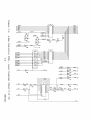
IOOIC DIAGRAMS
7.1
IN1'ROOIJCrIOO
Figure 7-1 illustrates the logic diagrams for the 4-Way Controller PCBA.
7-1
M8155A
i
I-'
(JI
~
I'Zj
1-"
~......
I
I-'
•
.a:.
j
eRa..........
,vEFE,vENC£
TI-4l!
DE.:ll'6NATJONS
NOT
{4:!1T U.3£D
TI-4e~
~
~
T/-lles
re
ac.
7~:5¢>l!
4'N
41"
71'.5'~_ --!SY
71'S"jj
.. SY
74S.31!
.. 51'
~L
~I
l!.T
-f/(4'T)
,
•
•
,
-fe
rSY/X
4'~
,v.3(/~)
C7,C"
~l!"I
C!!I
,.,
.. 1
NaOF PIN
:Y>AIt£5
yt!c.
tlJCArIOA DE: VIt!E.
1"4'
~
_r
~PAREe.
U1!J£D
Jf"
CS4'
DSI
e
~5V
74'5If!4ifJ
PU
-'-~K
PU
L>:~,1tP
1I.It!l..3
(1I1i!;;,~
(B
,
I
I
!1.~!.
I
"..51'
B Ii!
I
.. SV
.,2V
.. SI'
IX PU
.3.~X
Aq!r OF fjl'AIt£B
14'.I!i"
Z
7
S
'-15
1I.1i!,1.3.14'.IS
--4<"
~
......
I
tv
-=-
~
~1-"
..
n
TI-Cl!~
0
TI-C.H!.
I
-
r
~
~
~
0
, .1
I.
-I'SYPtt:
.TI-C/:!I
r-,--
i
~5e-S4'
r~YOC
TI-t!l!3
rt:.~
s·
'-0
ct.
4'7
l"t ,.
I
AI
~J~\I
-----.,
r--
II
IIC
PUI
e..
PU~
.3
PU.3
II
4'
PU4'
Is
PUS
I ....
PU....
I
7
PU7
(n)'
Jo.
I
I
I
I
II
II
I"
pus
PU~
'V
.AA.
"16
IL_________ .J
III
PUI';
PI/II
(e)
(..!S)
(s)
(S,7,B)
IRe.
-----,
ND
13. :>.<
(-4<,B)
(a,B)
(,,)
PU~I2.-1
l!
pu+r2.-2.
1.3
(4',S)
(-V)
(S)
(,)
1/
1(4'~)
PU"12~
(,)
LU+12-4
(,)
S
PU~12-!O
(,)
PuHL-C.
17
Pllt12-7
..A
I>
PlIt1L-8
..A
!>
..
(:»
4'
1("
I~
ill
I~
L ________ J
(!!I)
(:»
(!»
(,)
t:"(MI,ItV'f
n~.N£
""MI- ~
.:n/""'~ <??N"'/#
"'r~
_AEM
N-/.
15"-/~
I.$-/~
/J-/~
r~IM
I.I-IS
1.1-1'
/;-/Z
'I-/L
/I-/Z
'-II
9-1/
/ ' -'II
Z-<I
Z-~
I·~
,,-/
$-1
2-1
P6>A1 - PGol'l4
D~F1./DC.D
os"DeD
PuI.I.UP
I 5-"
I
'1-6
~,
1
i-l
ilD~"'f
•••••
(7) .
....
"
• 'eo
,,. - ,
(7) ' " " .
.&:a
!
~a
.....
.....
m =
-::Ji
),u~~-I
'"
(7)
.....
I
W
~
§
1
-
SD
_
J
~~
(I)
i.tIWDofDA'
-I
~D
~
I
--I>-
A13/~ "
II
7
,
I
AllIe. "
~
.
~
ILJ
4=--
~
:>
I
A13H,A
1.5
~
AIlIS,.A
IS
~
S
Alllto ...
17::<>----
.3
CK
/I
( ..)
CtA'
I'
~
(.)
T~.s; .. ~(.3 •..-)
A13~3'" (.3)
(.3)
~(.3)
I
IL. _ _ _ _ _ _ -.JI
IA>--
II
I
::!13
(
,
tf II 1 :j
•
~!:>
r-~~~-4-~--1
.3
4
ID
~D
7~f:e7.3
~ 3D
'-----"~::I4D
L----..:.:':==-t7 an
L. _ _ _ _ _/~*:~~~
'--_ _ _ _ _-"I.3=15D
(S) LDM:l,oDA'-
(I) ..!:!!!..
~~
TrClA'
J
~
,a
~a ~
I
.3Q~
I
4-61 '
IIQ~
~~ 15
SQ If!
Nt:!
AIlI7,A
~ I
r-..
A13/./J f'A
.:.'
~
i/"
A13I, .. A
..
e'
I I
~
!
AIJI!. -I-A
reT)
YECOr ~
0)
CMI!>ADA'.,. (7)
J
~
I~
w:::.-:-
I/~
II&>
I
A~/~ ~
AI'J/LJ .,.
(.3)
(.3)
AM7,
(.3)
,oats,.
(.3)
IA'
l/~l
I
L
74-l:ll!~(J
N . 3
I
L _____ ~ __ --1
:!1lFr.!1T.,.
AJ5~(3)
L________ .J
•
15
t<>~
1.3
f'..
II
I
I::!>
B
14
~
I!.
to..)
;a
J~. ~
,,'
J&;.k;K-
S'
11
~
1
i-l
-o
.... _
..
.w _ TN" 1
••
' . % , = - -.IT;
='5-
/I'
I
II
(I)
PlJl¢
,.~
7~.5f"
PlJ!i -
1
.."
A13~e.,.
7
TN.
Te-'-
r---~;---l
to
CJI
A13I45 _
LJ
It..
A13/.!1#A
Ii!
S6In
o
ii
i-l
e-
...
. . . . __
. . -.
I ..
r--
-Te-A4
-I.re-C~I
~~-A'
'=_."
=J"_<
A;g~
~72_-A...I<..'.'
"'!'~
,~""",,.
.M _
-
,
F~
.:.
;!E~
."J _ "',_"
1"_.'1
...•... _ 1,,-..
••
,._ 1,,_<,
A'!f!-1"-2-c4
~
~
~
A13II"
~
A-'I$5-
-'Ad~~
HLse~",
I ~
1-"
r
Jr-
r
_
n
i-
1
AJ5~SJ,('_r~
A~~1-T2_t:3
S
7ti1f.!;:---,
.:.a ~/S
SD
/I
PlJl
-"
U
.3a
ILJ ...
177D
1.3
~
"¥=
~
..
All~''''
~J
-~
110. I!!J
7 .3D
14
-e<=I
'.
,,0
1.<'=1
•
•
L<=i
..
H
I..
I"
-
IN
I!N
rI
e•
.... •
, ,
~ ID 7~l!:N!!7!!J ltil ~ I
~ i!D
~a ~
(s)
..--,=
••
1", u
• m
%,pg.
~
-;;....
,.
. 'M
,.
7D
' " ZIl",,.,.
'"<'A
(7)
(7) . . " .
~ ~
- '.
'
r
.....
,
-'
.. .. 5•
,
.....
.ns,.
(7)
(7)
A~"'A
~ ..
~ ~~7.3 -r.-.
~2I=:l/S ..A13~I4'"
T
Q
~
I
~.3 ~ ~5111f1~ .. "
.....I
•
A"!4=---l-T~-Ael
1,1'
7"LSc.,,~
_
5"
7
~!t
~
"'I!
l-=-!-4-'--
~
~
H
lib
III
AI!!4 .. (.3)
Ail/.!I ..
.3l,or.!1T -
-~
(.3)
('!J)
AI!>"I,
( ..)
A13~"
( .. )
IlE~Ir ..
(4 ,,)
AI!>~.t.. (..-)
I
IlEIrA' -
~/-t'I.!
;I-'
U1
ftJ
roz:J
l'
-..J
I
I-'
•
~
. _SY
r--ITD~-------lI
IR..5
I
I
1.3·'K
1~<5)
L. ___ ~- ; -
1
J
7-
'"
(i!)
h
~a
.....
.....
~
-..J
I
~
~
(C!) Al5cf'"
A<5I!!1_
(e) AI5I" ..
(i!)~
j
AtP
,
~;
5WI"
5We. ..
5W..5"
14 <512
I
(I)~
HijlJ
r--1I",
l! A<<5
4 A>.!I
-I 1.3-J!*
b- ,b - ,b-1
,
"
.,
.!I.3
.3 A=.!I
t~
f~---:r __
151
Ii'! AI
1.3 Ai!
15 A.3
1/ ~I
:SW4..
1/
ID
74ll5lJS
A = .7o ! ! m
A<.15 S
Nt:
A
At:
>.e
A.a
I
~_..
I
i'!
(e) Al5e3..
..5
,Ie)
A<5i'!i'!."
4
(e)
ALJel..
(5)
Fce..
"
.5
~
eli
.'\.05
.5 3'T
...
V.745;..r
ALJi'!I-A
...
A.lJDIi~SD-
HL<"~
l.!f
---.Ii'!
74LS/.38
4
I
~
If ~
IS
Ttl
I>
Nt:
r+
..3 C
LJ
§
N':
()
.5
CaHMCLIC -
(- ,)
J
PT"~T~<5 -
r-A
:!S~rR~r -
I
e
4P
.3
E.lJArINClK
(
•
7
)
74~;a
1-'-
0
0
~-
~K
~ ;Q;f74l5/3"-
(5) ,r-/W-A
5
(I)
u:l
i
-
(e) ~~.e/~CS-:.-."'_
(l!)
(o!!) ~.5"
r
~
0
I
~1i~r~N
6eLl
(4)
-
U)
'" 61
q~
!
I
Ie
1 LJ
~A
___
Nt:
EDArOUTEN -
(7)
I
~4
7..,514
w
~
ABI4 ..
PiN!
~~~--=~~~
ENYECr-
''''~H
ADDIiES.lJ .. (5)
JDTACX ..
(s)
I'1:j
1-1'
~
._-
(') PUS
~)
...,J
,
~
a
~SY
.--- ----------,
,~
.I.LJt~.o.(a)
~It l5 r!-NC
"
~
•
.a::..
~
PR
~D til'
.H
.LINT.., ...
(l!)
(t!!)
(l!)
(5)
i$)
(S)
(5)
AIJ1J3 ..
AlJill! ..
!l.-
~
Lf<
7+.51>+
I
13
I!
AIJ"I .,.
..3
f
JACK -A
~
....1J4>.3-A
.3;;..s KALFMrt: ...
I---.
C::-.3F
I
III
Ir~rL______.JI
J.3
I
[JoNT ...
IlJR ,. ...
Ie!"
,
J
H.5et..p!~
Ie
'---HLM/l
I
.31""V" ..;<.
41 "V"
-J;
JUSI-
GIL
I! D
I!E
er
IllI
"'55"
17
-I
ASS"'-l!
ASSA-.3
...,J
I
U1
1-"
n
o
~.
ffi
I!>
-
iI-'
U1
5fJ
7
..
41/F
~A
ec
I
SSEN
!!S
le r - - - - - - - - - - - . ,
/I
,
I
74:1$114
I
13
I
~
II
~
::~~
...
.o.5-A
I
I
1"6/-
'" L __________ J
1"61-
S.a...
eJ)
i!:J)
(I)
..3 c x " ~ f -
(I)
(5)
(e.)
Pt/(;.
Cl.Jt
I
H.$H
pus
MYrU~N~
P~
4 £
4
:I
5
I
IJr~K-A
£Ny£eT- (-')7,LJ,~
+
.31
'"
60YECr ..
-' rebo F-Nt!
I
74aS//
e.
(I) Pt/S"
ex
...
Q~
J(
AS ...
p~
L:'X
7 ...SIlI!
IS
Pt!>1! -
.3
r
.as
.DM460.,.
(5)
lJE1t1t ..
IJTACIC"
,,~
~
(I) PlIS
~...
Jt5T.L"~ -
II
~/.3
74.51><::
en
CI(
tiS"
4~
I
?<Io5H
MyrV,/PN-
(I)
~
~
(S)
I"'~":""
/l6ACK "..
S,7,.
dI~~
/.5
7<f'.5111!
PlI!>
P~
60'"
Ie
"/
n
0::'
!
,1"60'
I!£
745CY",;
II
-If'
cx til
~l:".
1.5
H.574
(I) PU5
PA.
/IT
DRlIlA.5 ..
-'t!. 4
(5.,)
HSI'e.
-::-
"til '
ex
eF
.liZ- Nt!
,!£K
CL~
'/p£S£T-A
.DlPlJU.5 - (
7<f'S;{!
,.§f~
1.1
(5)
I
~
STANT ..
~ 9t..
"/,p
WHOA,.
HSIL!
...
61'
JeD
/I
CCl.K-A
sroP-
PIP
FMArCH,.
HS;e.
is)
.!IE
..p
CK
i!F
I!K
{!~
..313£
I
(C!)
I
I
5
, J;
(S)
e
I
...t!!
~y,7.,..s
~IJ
IlJ6ACX"'· (5,7)
3
HS;P
----,
e
I-'
o
T/-AII
".
I PtJ~
()
l!
..3
/JP/P~ -
"
TI-AI
TI-CI
J'tI'.53.tJ
~AC
-4!Y
41J
111 IF
I ...
/Jp/f I -
'"
!l
P~IO
..3>' ~
/JPIPi! -
..3
(e)
.a::..
-
i!r
p~Ioe
74~e
(,,)
oc
I
:~.3
P/PIO.3 ..
#'
IT
PUt.. (I)
~
i
t il
I
f4<
74574
pbe.,.
'-'l
-
It:
7-O'51S7
I ....
<!A
/I .3A
ecl.":,.
~
§
IIJ
e
5
1-1
1-1
~
.3
b l!/J
I~ .3/J
-::-
~ ex Q Go Utili!.,.
I
- .- - - -r..J
~S~.3e.I
"'F.sA-I
AFSA-{!
AFSA-.3
.51 -v- -0 IN"
",I ""V" .-i. liS
L-::.'"___ .J
HI!
I
I
L_
I (IA) I
I I
le~
e I -v- ~!O
~4tSll4
I
1
f.!L1)
r-.s,-,
CUt
(I) Pllt.>
I
IR.3
3
.'"
21
I'
F"O-
-=
I,,,
I
~
L.:...-"::~.J
IIJ6,.t'.I:- (%)
i)
i
~
(JI
~
r-------------------------------~-----------------------------------~)
I'Zj
1-"
loT
~
(I) PiH
e.
.,
K
74'.sc"';
~
18
(
I)
PlI5
ID
I
II
•
i
~
IS
(.3)
I~"
L
~(4)
.!l
CCLI{"
COM'.:fl!tx -
~:;-
'Q
47
M
~
1.3
K.sT.bYTA(s) .s£TINrK
74.s,4
140
,.n.,,'j
.!:II!-- NI!
I 74SIIl!.
I~
W
.DIfTAOlJr -
(7)
~~~~
P/A#
I
II'~
"OMC~ _
(II)
KIfMC~
~Jtf/-
15
f
_
'"
("')
~
F6
'
~Ct!
l!C£ - (,,)
.sec ICE- (~)
c/'ItI!>USY- (fI)
IIJR .. A (4,S)
I
cu
I I NT'" f"
JIM
74iSI.3'
elf
~u
.. ~
~
4NG/ S
*. .
~A'14
II
/A
_1...d
I, 111
16
MItEO
~(4')
-V;:;;"
e
.. 1f/3
~(/)
11IR+
74£ SH
11111
(4')
:11
~::I
5-
~:E'~ ~;l
1'4
DATIN£N -
(7)
IH=ATJNEN -
~8)
4'STATEN -
.sE TlJU.sWK
.sET~.sItZJ
(8)
-
IN
~ ~LKIJKCU3 . •I1M-
(s) ""L.5Lr..
:1
1:1
74.se"1
~
/6
,~
1<
~
,~
L!LKI1K "I-
T,
(,)
CK3."'''M ..
(-:»
""ESET-IJ
(I:»
""E!Ur-A
(4')
~
lJ6Nr.,. (4)
7
.IA~X"
(4
reI! .. (.3)
S'
I.Q
il~ ~~~~
ttl I I I I I I I
"IV"" I! IAt!K-A
(4)
y#
YI
y~
1'.3
..
t.
b{!A
{;U
t.1
'5
LDt'£CT '4 .DIfTtWTCI It: 13
Ii!
(7)
U,3)
L DM'<;~(e)
l.lJhfIDAD" - (C!)
l DI ~AJJK - (/!)
_ ( ...)
::SETINTK _ (5)
~£TlJUSJ'
7".s;"
KLSLr". (05)
"
(7) ilnt .. A
(7)~
(7)~~
~7) LD~
~
7) .ED· ...~A~__________==::~
(7)~
(7)
.!J)",
fA
(7)~
,,~
SL
HLSe4S,u
S
H~
~~;
i!~...
'5 DI
Ie De
~! e~
.EDI..
AS
.?D.S ,.
II.
itD4> ..
ilD7,.
13 D7
AI
~
A'[~
A7 1,
A~
~!~:
itD4' ..
,
DS
CPU
(,) I~
(» _:I()r
mM>
(.3)
T
IVA
D~
':'111
(IJ)KE
(11)
.. 51'
-.111
ZIJ"'A
VI
-
I(
0
o
o
Ie
eL K
.LINT.., ..
n
~
I
.3
1'05
n-N
~
PV3
'"
~
r
.DK~u.s ~
!(l1)~·1
-
i
-
(I)
8
-- - .
(6)
~1-"
ADDH~~D
f"
~R- w
(+)
~
a
~
(4)
l
.3411
~
~
.DTACK".
(8) A'.s~
(5) ~,.
~
-.J
~e
13
(4)
(.3)
L!,r4M ... (S.~)
8
-.J
~
r-----'
ei 74'L~51 1
iV-A
..
..
~ ~
~~H>.
~ ~ ~ ~ ~ ~ 1I=_~~Ilr1=t~~~~~~~~~~~~~~~~~~~~~--------··-~~tS--(""~)
i1 1i-~ ~ ~ ~ = ~ :-:-:-:-~ :-~ =-=-=-~ ~ ~ ~=-=-~ ~ I- (~)
__
M
.::
""
_
M",,'. _
~A~~-("')
.? A~'- (4))
il~;- (~)
,,,..- I ' "
e",,p~ (.:,.)
"
,1.\
w'-- ,.)
("')
we-'·)
" " 1M'
",.IM)
I"Ij
~.
~
(PoT
(/;)1} A~ l:7t..'-2 at!
~ ": AI
611
&) ~ Ai!
ao
(!S) 2AtN
(5) i!Af!.
(5) ~~ti!.
(5) i!A~3
(5') il A~4
(5) ilAtP.5
....J
I
I-'
•
7)5 A3
"')4 A~
5~~ A5
(5') i!A~
~
(5) i!Ai"7
(5') ZA~8
!
(5)
~a
(.)
I
I
-.!.J
ZD5'A
/(P(/&)
6/7 I
i! Dt-. fA
(J~
(7)
(7)
~ (7)
II
.. sv
I~I
I I I I I I I I I I I PUll :H~" I I I I I I I I I I I I
"...
bN.D~I1')
e. Ne (A-I:)
(co::.) e$. ii£
(I
He v;'p
(i!7
NCo
(c4» AS
~c 1?'~-,".5Y
(eBI
i;z;M
(~",)
t:'£
~
....J
IA\
e.-;,);t; A/I'4>
lI-
....J
at.
A(P
cot') 1<:> AI.
KOMeS -
PUll
a.
05 15 17
_~_
ZA/~
ZAII
(.5')
(5) ZAIe.
(5)
0.3
:3) I A1
c!i C03 All
~i!~
~
~
~A (7)
i!h~ (7)
i! DC! • A
(7)
i!D3 .. A
(7)
~ fl4- fA
(7)
!iT
.'//'1
~
A8
cc A!'
(2«)
(e/) I~ AIO
§....
(])
rT..,;-,4'
'---___-=2I~If_O_-
(')
s)
1$")
(s)
s·
II
~AlHe~-
6HD It!
:i!
",AAI or"'''A
(e3) (!/L-wE) A/I
I
L _____
YCC
J
C! ) ' "
J.RD ZW'" -
(!
(!
21
Cl
(~)
~SY
C>~)
OZ
r-I·
(wz)
.5Y
L..._ _ _ _- - '
\Q
i
r
... ~c:.
MAH£BUSV-
74$t/J6
('K
~
u
131 IF
(s)t:'a6~"-
o
TH£S£ I"AR1.:3 A"'~ c!4'-PJN ~UYIt:'£3 IN5TA~L£.D IN
cB-PIN
.DIP PA'TUfN~. THE. ~&£A'5 IN
PAA'£IVTN£5I:5 INDIt:'AT£. TN£. 1!8-PIN £.QI/IYAL£.HT5
J
/I
1'1536
lJ IJ
MYBERR. (b)
5/
/!JUSY,... (7.a)
B
HC
NC
LQR
L.£i'"
~
-
(,,)~
p,(>
....Q(!!J
~
I-'
0
(Z)~
5
('T
U1
f
L~ ___
(5) SErBUS Y (.3) COO1MCLH _
-
iI-'
-iF~
1.3
74'(.574'
O)ClRI£D-
TI
74£$7'1
;...
U'I
~
r-z:1
.....
1
.....
...
•
I
~
j
~
II(
~
fJ-e:Ai!7
IJI!>~7.DI!> ~t. -
,5 A7
~~
~;E.TC'-Ai?i! r.: i"i:
"ALJ
LU,
liAS~l!Jo5
7 At.
I!> 41>
~~~~e-
;
1!>.3
~5 .DI!JN-'-=-'-'=
..; AI
Ae
~~
DI!>.3-
(+)
DATAO(ITEHUt'T-
i!
I
4~
.3
£DAn:wT
~
~
~
~
0
I
DATIN£N-
e.
.3Q
t.
.lD7~A
~D"''''A
i!DS-.-A
~D4
~
461
Ie
561
IS
'-0
It.
70
1'3>
"
/!-
/IJ Hi.B.3N /tfl
liD
17 7IJ
1,5 BD
I
(05) DArOUTCU: -
1/
2
alii
".A
~D3
... A
~De ... A
JD, .. A
_D; ... A
.5D
(e.,s.'-,8.'.!})
(c,s,t.,8,'.!})
(e •.5.11,,.,~
(e,5,,,,,~=:»
~,5,t.,o!),~')
(e,5,t.,8,!»
(e,5,t.,,..~)
(E • .5 , t.,&. !I)
Ol
CI(
I.D
.31(
74l:5374
'-; eD
161
elIl
3.11
4IJ
13
SD
...5Q
/4
-
..
2,,)
7
D
~
/3
I'"
IT
/.8
1!>00ADsrLN-
l!D
10i
(I) PlH
/I
6
e
'''''
~HS24J
.I£D~+
r--------,
~
',4 .rlI)~-
",i
~4SZ+4>J
_
-------
.
L_______
£DAUNCll(-
~ 4~
t-
.3 DArINI!LK-
I
e.
(a)
"l.
74~.!>e
DArIN
~4.s4>.
'"
(+)
I~~AC.c ...
(s) ~K
~
~
t.
IV A
~
B
1"14I)
841
-
~
/"
~
eQ ~
t.
.361
4a '3>
/(?
.:1"61
u.Q /SIt.
761
IJQ
/:3
(.3)
£DArOUT£N-
( ...)
IJAI!>U.5-
1f;;)
6
74~3l!
elf
3D
4IJ
..0
t.I)
7IJ
IJ
,------,
ilJATINCLK-
4GO
It!
sa
/Slia
III
7Q
21 II) ? .... 53?.3
/0
(,,) D.<;,'m~ D5RCDSIi'I!>
(!» IJ5IPA (2) ;'/(.'T ~
(e) C.HI!>AlJlP ~
(e) SlFTS T".
(t.) I!>USY f-
..
~
(.3)
I O£
II
t:'1C
lDY£CT-
£DS-
H:S;fJ
/T
TIJ
/8
AD
(..3)
(s)
O£
CI(
~
b
(5)
~
eo ~
t.
210
461 I!"
Ie
sa
IS
6&1
I.
761
r-:!.
f-?
s·
.....
17
(5)
eD
3IJ
Z>
4IJ
1.3
SIJ
14
~
cT
"'
IQ
ea .5
.3D
,5
4.ll
1.3
5D
1+
(PIJ
TD
LJD
.Dille ..
DIl(lI ..
.Dl!J¢(J ...
.3L
0
f
IS
21M
7*l5374
~D
7
.D"J>..3 ..
lIP
D
-
()
-
13
.DIIt
~.....
i
/<9
I
4
H:5fIB
.....
~
0)
iJl
I!JZ
.3
IJl!>f7 ...
IJf!,Ij>{J> ..
.l!~(lS- ...
.DEI~4 ..
/I
-fo
-I I
)
(5
A.3
iJ4
~r4A~i-
[
.....I
UlS"'~",5 7 Ie
rIJATOur~N-
r=-.:,.
IJArOUT£N-
(I!J}
t'lj
1-"
1
....,J
.1•
IN
)
(
(;)
(4)
5)
)
' " aD
Z.f- W
"
(:
7G1 114
1:3 SD
5Cl
I71i.....
~
/J 4IJ
~S
Ii!.
~.,
;
:a
IW$Y
DATOl/TCllC _
DATlATCH .,.
( )
(5)
~
!
~a
.....
.....
I
\D
..3 ID
(I) PO'f'
/I
1
4!STATEIY -
(5)
tlI 5
(7)
DATOi/TEN -
~
•
.L
e
10.
I II
J
,zD'"
I
;£D7
I;;
7'f'sf6f6
ClN
(5)
(5)
~
IU5ET-tJ
1.3&"
I.EDOFF -
7-#s~a
.
CtllUD -
t
II
7-#t:57-#
(,>
e£
D1!115 ..
I!J 4I-D
7 3D
DIJ/'f'-;
IiIJI3 ..
/I
.IJ~Je
17
'"
..3
1.3
I'f'
17
16
.,.
.DB 1/ .,.
Iii!./j" ..
D13t.!> ..
D'-',ps ..
IS
I!>
&,
1-#
/J
Ii!
(7) DAT.fNt:'t.k -
(5) M~AT.fNEN-
eD
IIJ
7""I..5.3H
!>
...41
tP
;~
5
161
5D
J.,D
7D
Ie
so 15
"0 It..
IJD
1!J4l
761
I:'J
1'1, "'A:
14 o..!
'---------'
...
(I)
I>t/~
5~
t.
...
(5) REs£r-.a
I
1-"
r
~(S)
( ...)
.D1I11U:5 -
( ...)
LIYYECT _
~
7.,5""
~"
S'
(.5) ~WN
It!.
~ 1/
_
(~
10lla-
I.3J~.e
IO/fill ..
(5")~
c:c
f-&
VI
~
~
f-&
C
-
-
(j)
IVNITE -
(,)
tl~e
:STA.fTACJ(.,.
..3
.,
(5")
CK-#M ..
e Ii
_ _.!::;!.l~~
L _ _ _...!.ct3~5.D
~_ _ _-<.14 &.D
745'4
~LAD-
_
<=4
(5,£>
7""t511
ID 74t:se73 10 ~
7
L
Aft ..
&!.fD1NTND-
..36
e I-f'F).3
745;8
;
(.5)
FF.3FF'f' ~
FFCFF3 ..
US(J4
OC
~5TINTA
(.."s)
7-#.51"
i
t il
~STItJlI
7"".sp
NSf--
(Q
-
.A
NS
p-'l,-~_ _-,~=-r.:...:l:.:£:.:IJ",GW=_-":'''''-_~H''I-+_ _ _ _- - I
STt.EIJOIY..
(7)
(7)
(7)
(7)
(7)
(7)
(7)
(7)
-;Sy
(;
DC
Q .:. lYe
CI
§
o
-
(.) /tIYBERR+
.....
....
....
~ ~:. ....
I
.N
~
n
LEDON
t.a
~~
~.J)qJ
"5~: 'A
e.vc
'~D.3...!rA
.. A
•
IYC
~
....,J
ao. I:'J
7D
14 bD
..EN.....
(
7'f'£5:37:3
CtwMAND.,.
.
eo
JINTAI!J( ...
5
t.
!>",c.
•
~INrA"',c-
(:»
745;'f'
:!:
..,
.50
INT~D •
!>
A "'I!. IJ
Ii!
11#0 15
WAIro'~t>-
17 7D
70 I~ NC
IS /JD
/Ja "
5
/I
~Ir ..
~(5)
7-#tSJI
NC
~Cl~
~C'~
FFSFFt.> ..
,." +
(5")
....~
_I
(JI
5C
(e)
5LFT.'JT-
(~
(7)
;ED7 .. A
~/cY
~~
I'1:j
1-"
~
'-01
I
....•
~
j
~
........
a
(7)
SF
ZDII,A
.,
Z DS , A
(7) i!D3" A
(7)
(7)
(7)
(s)
e.
-i!.Dl! 'A
i!DI,A
i!D~.A
T
:;:~/C£'
11
-.1
(B) -;;;~-rL (8)
S
)
~)
UNrACK
D~
~
o
HrSA _
~
I/J
cr.!lA-
iiW
'"
DT~A
.iil'liA "
~~ Co!
:;,~
::> _
~.,c}-a
~/"a"
i!
-
11111" "" I"I
T JlDIJ ..
Ie r£I
TeB KrJlCA
/fJlD!!. ..
~
I~
I!
I
"
~
el!.
1.,8!:>
2 .. 1 .
I~
O'S I
H Q
Q 13
I
T
I
II I~
-_
DC DA t A
CTSA +A
DTRAtA
PI-
~~~r=-;;-,
~
I
I
,,0
.
I
.!SYNC"
TKxCB
i'
e",
w7~u;,a .3
-
/"'0
7
N7
-::r¥
L-'IIII\r-
PU'~-~
(5) 5ccleN.
~I'=========tI· Iffl~~~
.Iev
~
rXDA
15
TX.DC
HXDA
1.3
'<:XDt:. ..
Hr.5A
"
A'rsc -
__
croSA
IIJ
<!rsc _
j)j';i;;
/r"
DT~C
DCDA
I!J
IJCDC -
'---------------~-fe~PCLIt: ~~I
TK~CA I ... Nt!
~ wln.QA /, Nt:.
L-_ _ _ _ _ _ _ _ _ _ _ _ _ _
r
~.-ll"
Dr~~
/"'JJ~
5C
e
u-C
/.,._
ND
I'QI
/~8~
11J:':l/.3
-'
I~_
.3
SIJ
I('TSC
A
•
-,Ie.
/"8~
I
1"8~
I
I
I
DCDC,....
CTSt:. ... A
D511t! - (~)
~
1
/~Q
I
I
II n
DTRC ... A
Ct: ... ~
~
NT~~A
.rl
I
9/-'1
I
Y
OIS
0"
: r-O
I
DS~J!J -
PI! : !>
(7
,
'S)
IJ.<:,
A!-~
TADC -
@:::zJ
0
n r
Y
5
0
P.5-
DCDC+
1P.5 -7 I
I
NT~C"
I P3 -.3 1
I
PU fie -5
I
I
j4 Q
O.3!
e
01
L _____ -J
II)
PUlli'.-U>
(t)
~
-=-
ersc .,
DT~C.,.
l,r.3~ L!
14~~
14
e~~
~
,.
'<:XDl'.-
I!J I
1 ~_
I
_~/::l4'
--
P6M
I H~-v
_,
AC"
l.j
r-
,.r
B 5A
~
4)..l.. '-------'
,-
CTS.!I-t-
•
~
- /.,._
511
-
[£dINT
~-I.LEO
\D
/.,.086
~
....o
-
(.)
PU'!e.-4
...-J\I\I\r-- -II! V
.---JVV"v- -Ii! v
f5CI!
~------
~
RTSl!It
~
CTS8,A
RL!
1'#""
8S.30
c.Q
r
~-e
I PI!-7
+
DCD"
.DTl<oS -t-A
n
i
-
~
A')(DJ!J _
I
N9
s·
~
~IC
~(s)
~...,.
.
rXDI!.
I
-1i!V
Ip/-::> 1
(7.)
.D:S~A
IJSI1 ... t-
::>1
~A:
PI-"
.DUA..
:
~-Ie."
L
JIH~ 9 /.51
Na
~)
CT.5A.
0/5"1
;~;::~
NID
~
(.)
PU#/I'!-/!-
r1 p6Me- ]
rXDl!.~/II>-
Nt!
II
s IiI:
/.,./1,
":-~----In
~('!»
0
_:''!._~/J_
i
'<:XD8~/!!>
1PI -..3 1
/>Ut//!-I
/ -'c .3
IJ DoS-
I
PI-~
~
~
A'T.5A t-
~6~i
------~T".'JIJ .DTKIJ
1
I
1 . I.
I
II ~
~TSIJ
----
I
':
I
r
.DCDA.
I
0 7
I PI -
HXDA -
I
0"
r-=;---;-'1
I
I
I
rXDA -
i
I
1-'16
I
Rrs A t-A
1
III
i
I
I
/41!JB
j;:~x
-'I
I
'~"'!:J
~
e~
7 Pt!LK
".sy
"'..,.
i!B
I
-ACY
IlS.30
SCI!
RX DAJ/3 -
~ ,"/J'!:J
"I
(,)
IJSItA -
I
.3
-leY
~ ~rJlcoS
T I
4t!
L:::I /.,,,,,1
DCDA -
/I
TXDltJI~-
II
I~"a
...3 e.l!.
..3e. Dla
~
'-01
17
5YNCA
(s) CK.3.t..IlM..
(
~XDA'
.3~ A/;i
(s) i!A~"
(s)
PUB
ClKBR"
D4
""-s1.,;!'
rXDA,
13
HT~A
.3::> D.3
..../ De.
IJI
..3S
i!!A~S
~)
A'~DA
.37 III
.3 Dr..
' . 3 0 8 DS
(7) i! D., .. A
rXDA I!J
.
r--------,I
'!:JI
.,.5Y
I£O~CCI! ""Ne
/"II!>
D5KC -
.~_ ..........
I
P.3 -.q
I
P..3-'
(7')
#
I'Zl
1-1'
1
TI
TI
el
ce
C!>
eof' eU'..3:;1iM(5)
~PAIfE.
cs
FCI-
~
I
.....
•
~
AI3
AN
AI5
A/~
All
AI8
AI!)
a
.....
.....
(5)
.IACK 6ND
(s)
C'II
CIl!
CI3
CI.,
CIS
CI(,
CI7
C/~
~S V.D~
""6ND
,.~
~
CoND
.. S VDC
.. S "DC
6ND
.. s "DC
'5" VDC
tJ.ND
~
§
INT., .INTe. -
C~
C'
SPAIt£.
~
I
~Plte. - (of')
I5PNP- ( .... )
1S6ACI<::... (5)
/jN - (s)
6ND
INTt.>-
C1
CI!>
~
1-1
1-1
~
C'~
bND
IPE.SE.T- (s)
l>ND
~
I
6ND
.. 5" "DC
.!SPANE..
C.51
C!>,'!
bND
PFDr
6ND
IfUJERrED
/jPIf 1/jlRRlJ6IVT aND
INT7INT.5 .INT.3INTI6ND
.. S VDC
SPAlte
-II! .,DC
bND
.. /~ rDC
... S VDC
6ND
.. 5VDC
(.,.)
(e.)
(5)
.. S "DC
6ND
VDC
'DC
6ND
PI
.. S
.. 5
I
l!
..3
....
S
~
7
&
~
.Fe
PE!.
T.I<D~
NXDA -
('!»
(!J)
H'~~
(,)
e
7
SA,!....
D?~
6ND.
DCDA..
~")
!»
(,)
(~)
Ity~_ (~)
Dr~ (!»
.Fe
,,f-T
~
7
IT
f-iT
7~
P.5
TJI~-
N"D/j -
A'T.5.5 .,.
cr.:s~
..
D~It/j..
6ND
.DCD/j"
ItJ/j"
DTit/j ..
('~)
(!»
(~)
(,)
(!iJ)
l')
,)
,,)
C')
,,f-F
~
f7
f-T
f-if-T
f-i1-3--
TXDCRXDC-
(~)
(,)
RT.!SC+ (,)
CT.!JC .. (!»
D:!JltC .. (!i)
6ND
DCDC ..
RIC"
DTNC+
(,)
(,)
~~)
!I)
-
r--r
'"F
~
~
fs
r,;--
~
~
~
TJlDD NXDD ItT.!SD"
(~)
g)
c!»
i)
C T5D ..
DSltD .. ( , )
6ND
(,)
IlCDD" (~)
RID .,. (~)
DTltD .. C~)
~,
n
-=
S'
~
i
-
r
('T
.....
0
~
.....
V'I
~
~
.....
0
A321
_,rAJ
LTHI~
StG.NA.L
IS TIEP TO
TliE JI\OUt-lTINcit
HOLeS
OF
e~
C:O"'_c.'TOl!.
-=
M8155A
7-12
APPENDIX A
LIST OF IffiIC
D~ ~CS
This signal enables the 4-Way's internal status onto the
Z-80A's data bus.
A=B
This signal indicates that the 4-way has been addressed.
AB01 - AB23
These signals are the EBUS address lines.
This signal indicates that 'the 4-way has been addressed and
enables the slave mode registers to be accessed.
AFSAl - 3
These signals are the switch selected first stage arbitration
level for DMA and Interrupt arbitration.
ASSAl. - 3
These signals are the switch selected second stage arbitration
level for DMA and Interrupt arbitration.
AS
This is the EBUS Address strobe which indicates that the address currently on the EBUS is valid.
This is the EBUS generated Bus Error signal which indicates
that an operation on the EBUS was unsuccessful.
This signal is the Bus Grant Acknowledge that is generated by
the requesting device to acknowledge being given control of the
bus.
This is the Bus Grant signal generated by the CMB to glve control of the bus to the requesting device.
This signal is a slave mode command to place the 4-way's Board
status on the EBUS.
BPRO - 2
These EBUS signals determine the priority
DMA or Interrupt.
BR
This signal is the EBUS Bus Request signal that
the device requesting control of the bus.
BUSY
This signal is generated by the Z-80A to inform the CMB that
the 4-way is currently unable to receive any new commands from
the CMB.
This
CK3.68M
1S
arbitratio~
1S
during a
generated by
the 8 MHz system clock.
This is the 3.6864 MHz clock required for the see chips to generate the required baud rates.
A-I
M8155A
CK4M
This is the 4 MHz clcx::k, derived from the system clock, required for the Z-80A.
This is the split baud rate clock, generated by the CMB, required for uses when the serial transmit and receive clocks are
different.
CLRBUSY
This signal clears the BUSY flag given to the OMS.
This signal clears the Command Receives flip-flop that informs
the Z-80A that a cammand was received.
This signal turns off the LED.
This signal informs the CMB that the base command block address
is required by the 4-way.
This is the status bit that the Z-80A reads to determine if a
command was received.
;
This signal latches the new command and sets a flip-flop that
will inform the Z-80A that a command has been received.
C1'SA - 0
These are the Clear To Send signals required for each of the
RS232C ports.
This signal informs the transceiver that data 1S being sent to
the CMB.
This signal latches the data being brought onto the 4-Way from
the CMB.
This enables the lower. 8 bits of the data brought 1n from the
CMB onto the Z-80A data bus.
This line informs the Z-80A that data has been latched for the
CMB and it has not yet been used.
This signal latches the data on the Z-80A data bus prl0r to
sending it to the EBUS.
DATOO'l'EN
This enables the data onto the EBUS from the 4-Way.
DBOO - OB1S
This is the EBUS Data Bus.
DCDA - 0
These are the Data carrier Detects required for each RS232C
serial port.
This signal starts the DMA cycle after completing arbitration.
mBUS
This signal activates the data drivers during a DMA cycle.
OORA - 0
These are the Data Set Ready's required for each RS232C post.
M81S5A
A-2
This is the Data Transfer Acknowledge signal. This signal is
generated by the slave device to acknowledge being addressed by
the master.
lJIRA - D
These are the Data Terminal Ready's required for each RS232C
p::>rt •
This places the data to be sent to the CMB on the EBUS.
This signal latches the data or command being 'sent to the 4-Way
from the CMB.
This enables the data onto the EBUS as a slave mode read operation.
This places the Interrupt Vector on the EBUS data lines for the
CMB to read. It also terminates an interrupt operation and
resets the interrupt request.
This signal is used as a timang signal for the DMA circuit at
the start of the cycle.
This signal indicates that both stages of the arbitration
passed.
00
This signal informs the DMA circuitry that the proper conditions exist for a DMA to take place.
This signal informs the interrupt circuitry that the proper
conditions exist for an interrupt acknowledge.
This signal informs the arbitration logic that a level 4 interrupt has been acknowledged and starts the arbitration sequence
to determine if this board is being acknowledged.
IACK
This signal is sent by the CMB on the EBUS to acknowledge an
interrupt.
This signal is the Internal Bus Grant Acknowledge which informs
the address drivers to place the DMA address on the EBUS. This
signal also drives BGACK.
IBR
This signal is the Internal Bus Request that will drive the BR
signal on the EBUS and will start the DMA cycle.
This is the Internal Data Transfer Acknowledge which informs
the CMB that the 4-Way has acknowledged a slave mode request.
IINT4
This is the Internal Interrupt request that starts the interrupt cycle and drives the interrupt line for the 4-Way.
This is the delayed read strobe required by the SCC's during an
interrupt acknowledge.
A-3
M8155A
lCEQ
This 1S the Z-80A's IIO Request strobe.
This strobe allows the Z-80A to load the lower 8 bits of the
DMA address prior to a DMA cycle.
This strobe allows the Z-80A to load the middle 8 bits of the
DMA address prior to a DMA cycle.
This strobe allows the Z-80A to load the upper bits of the OMS
address prior to a DMA cycle.
This strobe allows the Z-80A to load the interrupt vector prior
to an interrupt cycle.
T.FJX)FF
This strobe turns off the LED.
This strobe turns on the LED.
This is the memory request strobe of the Z-80A.
i
This strobe enables the upper 8 data bits latched from the CMB
onto the Z-80A data bus.
This signal indicates to both the DMA and Interrupt logic that
the 4-way has successfully completed arbitration for the bus.
PRIOl - 3
These are the boards bus priority lines which are compared with
the priority lines on the EBUS.
This signal is the RAM chip select.
RFAD
This is the read signal that the see's rece1ve.
RBJl - 2
These are timing signals used during arbitration.
RESEt
This is the reset signal received from the EBUS and used to
place the 4-way in a known condition.
RIA - D
These are the Ring Indicator signals required for the RS232e
p:>rts.
RCJtC;
This signal 1S the PROM chip select.
RSTIBR
This signal resets the internal bus request.
RSTINIR
This signal resets the internal interrupt request.
•
RTSA - D
These are the Request To Send signals required for each RS232e
port.
RxDA - D
These are the Receive Data lines required for each RS232e port.
SCC01CE
SCC02CE
These are the see chip enables.
M8155A
A-4
This signal sets the internal bus request signal and starts a
EMA cycle.
SErBOSRD
This signal sets the Il1A circuitry for a read operation.
~
This signal sets the I:MA circuitry for a write operation.
SE1'BUSY
This strobe sets the BUSY bit in the status register.
SETINTR
This signal sets the internal interrupt request and starts the
interrupt cycle.
SLtifST
This signal is activated during the self test portion of the
firmware and disables the data drivers to prevent unwanted
characters from reaching the screen.
This signal is a' slave mode reset to the board.
This is the second stage enable of the arbitration logic.
This signal starts the driver bus portion of the EMA cycle.
This signal starts the wait cycle necessary for the Z-80A to
acknowledge an sec interrupt.
SIDP
This signal starts the shutdown cycle of the EMA in progress.
Txm - 0
These are the Transmit Data lines required for each Rs232C
port.
This signal informs the CMB that the base interrupt vector 1S
required by, the 4-Way.
This is the wait strobe that is sent to the Z-80A during an 1nterrupt acknowledge to the sec's.
This turns off the wait line after the wait states are added to
the acknowledge cycle.
This signal is activated during the shutdown portion of the
current DMA cycle.
This is the write strobe that the sec's rece1ve.
ZAOO - ZAl3
These are the Z-80A's address lines.
zoo - 7
These are the Z-80A's data lines.
This signal indicates that the Il1A circuit 1S bringing in data
from the CMB.
ZIlATOOTEN
This signal indicates that the DMA circuit 1S sending data to
the CMB.
A-5
M8155A
M8155A
A-6