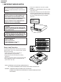
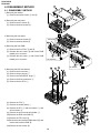
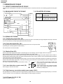
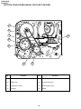
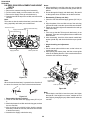
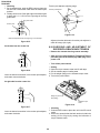
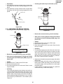
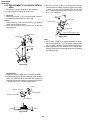
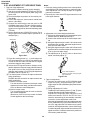
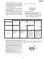
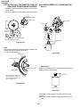
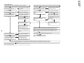
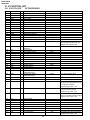
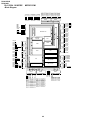
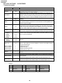
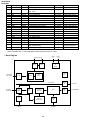
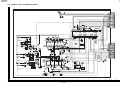
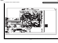
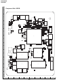
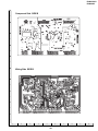
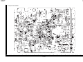
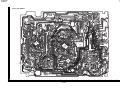
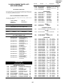
1
DV-NC55S/H
DV-NC60H
SERVICE MANUAL
S01B9DV-NC55S
SERVICE MANUAL
VCR/DVD COMBINATION MODEL
REW
PLAY STOP
PLAY
EJECT/ STOP
POWER
OPEN/
CLOSE
STANDBY
/
VCR DVD
(AV 1 )
CH(TRACKING)
AV 2 IN VDEO L(MONO)-AUDIO-R
DV-NC55S/H
OPERATE
DVD / CD / VIDEO CD PLAYER
EJECT/
STOP
/
REW
PLAY/X2
CH
REC
DVD
OUT
PLAY
STOP
VCR DVD
(LINE 3 )
OPEN/
CLOSE
LINE 3 IN VDEO L(MONO)-AUDIO-R
MODELS
DV-NC55S
DV-NC55H
DV-NC60H
VCR/DVD COMBINATION MODEL
In the interests of user-safety (Required by safety regulations in some countries) the set should be restored to its
original condition and only parts identical to those specified
be used.
DV-NC60H
QSURROUND
CONTENTS
MODELS DV-NC55S/H/60H
Page
1. IMPORTANT SERVICE NOTES ........................................................................................................ 2
2. FEATURES ........................................................................................................................................ 3
3. SPECIFICATIONS ............................................................................................................................. 3
4. PART NAMES .................................................................................................................................... 5
5. MAINTENANCE CHECK ITEMS AND EXECUTION TIME ............................................................... 9
6. DISASSEMBLY METHOD ............................................................................................................... 10
7. OPERATION OF PICKUP ............................................................................................................... 14
8. ADJUSTMENT, REPLACEMENT AND ASSEMBLY OF MECHANICAL UNITS ............................ 15
9. ELECTRICAL ADJUSTMENT .......................................................................................................... 38
10. TEST MODE .................................................................................................................................... 41
11. TROUBLESHOOTING ..................................................................................................................... 44
12. IC FUNCTION LIST ......................................................................................................................... 58
13. BLOCK DIAGRAMS ......................................................................................................................... 82
14. SCHEMATIC DIAGRAMS ................................................................................................................ 92
15. PRINTED WIRING BOARD ASSEMBLIES ................................................................................... 114
16. REPLACEMENT PARTS LIST ...................................................................................................... 137
17. PACKING OF THE SET ................................................................................................................. 159
SHARP CORPORATION
1
DV-NC55S/H
DV-NC60H
1. IMPORTANT SERVICE NOTES
Note:
This unit can be used only where the power
supply is AC 230V-240V, 50Hz. It cannot be used
elsewhere.
CAUTION:
USE OF CONTROLS OR ADJUSTMENTS OR
PERFORMANCE OF PROCEDURES OTHER
THAN THOSE SPECIFIED HEREIN MAY RESULT
IN HAZARDOUS RADIATION EXPOSURE.
• This Unit is classified as a CLASS 1 LASER
product.
• The CLASS 1 LASER PRODUCT label is located
on the rear cover.
• This product contains a low power laser device.
To ensure continued safety do not remove any
cover or attempt to gain access to the inside of
the product. Refer all servicing to qualified
personnel.
CLASS 1
LASER PRODUCT
DO NOT STARE INTO THE LASER BEAM OR
VIEW WITH OPTICAL INSTRUMENT.
WARNING:
TO REDUCE THE RISK OF FIRE OR ELECTRIC
SHOCK, DO NOT EXPOSE THIS EQUIPMENT TO
RAIN OR MOISTURE.
(Rear of product)
TO REDUCE THE RISK OF FIRE OR ELECTRIC
SHOCK, AND ANNOYING INTERFERENCE, USE
THE RECOMMENDED ACCESSORIES ONLY.
Laser Diode Properties
Material: AlGaInP
Wave length: 650 nm
Emission Duration: Continuous
Laser output: Max. 0.7 mW
Power Lead Protection
To avoid any malfunctions of the unit, and to protect
against electric shock, fire or personal injury, please
observe the following.
• Hold the plug firmly when connecting or
disconnecting the AC power lead.
• Keep the AC power lead away from heating
appliances.
• Never put any heavy object on the AC power lead.
• Do not attempt to repair or reconstruct the AC
power lead in any way.
VARO! AVATTAESSA OLET ALTTIINA LASERSÄTEILYLLE.
ÄLÄ TUIJOTA SÄTEESEEN ÄLÄKÄ KATSO SITÄ OPTISEN LAITTEEN LÄPI.
VARNING - LASERSTRÅLNING NÄR DENNA DEL ÄR ÖPPNAD.
STIRRA EJ IN STRÅLEN OCH BETRAKTA EJ STRÅLEN GENOM OPTISKT
INSTRUMENT.
2
DV-NC55S/H
DV-NC60H
2. FEATURES
Ë Common Features
• A DVD, AUDIO CD player and VCR all in one.
• Simultaneous VCR recording and DVD playback.
Ë VCR
•
Hi-Fi Stereo Sound/Double-Azimuth 4-Heads
• 1 minute Rewind (E-180)
• S-VHS Simple Playback
• HQ (High Quality) Circuitry
• Simple Recording Timer
• Sharp Super Picture
Ë DVD
• Plays DVD and Audio CD discs as well as CD-R/CD-RW discs recorded in MP3 file format
• Virtual Dolby Surround (QSURROUND*1) provides high-quality surround sound
• Digital Gamma correction and Digital Super Picture functions
• Dolby Digital*2, DTS*3, MPEG Audio digital out capability
• High-quality digital images
• High-quality digital sound
*1 QSURROUNDTM is a trademark of QSound Labs, Inc.
*2 Manufactured under license from Dolby Laboratories. "Dolby", "Pro Logic" and the double-D symbol are trademarks of
Dolby Laboratories.
*3 "DTS" and "DTS Digital Surround" are trademarks of Digital Theater Systems, Inc.
3. SPECIFICATIONS
Signal System: PAL
INPUT/OUTPUT JACKS
DVD/VCR shared output jacks: VIDEO jack: RCA Pin-jack
AUDIO jack: RCA Pin-jack
DVD output jacks: VIDEO jack: S-Video jack
AUDIO jack: RCA Pin-jack
DIGITAL AUDIO IF: Coaxial digital
AUDIO output jack: RCA Pin-jack
VIDEO input jacks: VIDEO jack: SCART
AUDIO jack: SCART
VCR
Video Recording System:
Number of Video Heads:
Video Signal Standard:
Audio Recording System:
Rotary Two-Head Helical Scanning
4
NTSC Colour System
1 Stationary Head for Linear Audio
2 Rotary Heads for Hi-Fi stereo
Tape Width: 12.7 mm
Tape Speed (PAL): (SP) 23.39 mm/sec
(LP) 11.70 mm/sec
(EP) 7.80 mm/sec
(NTSC) (SP) 33.35 mm/sec (Playback only)
(LP) 16.67 mm/sec (Playback only)
(EP) 11.12 mm/sec (Playback only)
3
DV-NC55S/H
DV-NC60H
Recording/Playback Time: (SP) 240 min (With E-240 Cassette)
(LP) 480 min (With E-240 Cassette)
(EP) 720 min (With E-240 Cassette)
Channel Coverage: UHF E21-E69
Antenna Input: 75Ω
Video Input: Input level: 0.5 to 2.0 Vp-p (75Ω)
Video Output: Output level: 1.0 Vp-p (75Ω)
Audio Output: Output level: –3.8 dBs (47kΩ)
(0 dBs = 0.775 Vrms)
Audio Output: Output level: –8 dBs (1kΩ)
(0 dBs = 0.775 Vrms)
Hi-Fi Audio: Dynamic Range: 90 dB
Frequency Response: 20 Hz-20 kHz
Memory Backup: 60 seconds (55H/60H)
60 minutes (60S)
DVD
DVD/VCR shared Video output: Output level: 1 Vp-p (75Ω)
S video output: Y output level: 1 Vp-p (75Ω)
C output level: 0.286 Vp-p (75Ω)
Audio output: Output level: 2 Vrms (1 kHz, 0 dB)
Video signal horizontal resolution: 500 lines
S/N ratio: 60 dB
Audio signal frequency characteristics: For DVD linear PCM playback:
4 Hz to 22 kHz (48 kHz sampling)
4 Hz to 44 kHz (96 kHz sampling)
CD playback: 4 Hz to 20 kHz (JEITA)
S/N ratio: CD: 100 dB, 1 kHz (EIAJ)
Dynamic range: DVD linear PCM: 96 dB (JEITA)
CD: 96 dB (JEITA)
Total harmonic distortion ratio: CD: 0.006% (JEITA)
Pickup: Wave length: 650 nm (DVD) / 780 nm (CD)
Laser output: Max. 0.7 mW
Operating temperature:
Storage temperature:
Power supply:
Power consumption:
Dimensions:
Weight:
5°C to 35°C (41°F to 95°F)
–20°C to 55°C (–4°F to 131°F)
230V-240V AC, 50 Hz
29 W
430 mm × 99 mm × 363 mm (W × H × D)
6.3 kg
Specifications are subject to change without notice.
Weight and dimensions are approximate.
3-1. ACCESSORIES
Accessories:
Remote Control Unit x 1, Battery x 2, 21Pin Cable x 1, RF Cable x 1,
Operation Manual x 1, Quick Start Guide x 1
4
DV-NC55S/H
DV-NC60H
5. MAINTENANCE CHECK ITEMS AND EXECUTION TIME
MECHANICAL PARTS REGUIRING PERIODICAL INSPECTION
Use the following table as a guide to maintain the mechanical parts in good operating condition.
Parts
Pickup
Spindle Unit
Sled Motor
Loading Motor
Belt
Note
Maintained
1,000 hrs.
2,000 hrs.
: Part Replacement
: Cleaning
(For cleaning, use a lint-free cloth danpened with pure isopropyl alcohol.)
CARES WHEN USING THE PICKUP
1. The laser light having wavelength 650 nm is emitted from the objective lens. BE CAREFUL SO THAT THE LASER
LIGHT DOES NOT ENTER DIRECTLY INTO YOUR EYE.
2. The semiconductor laser may be easily damaged by electrostatic charges. When handling the pickup, take care so that
the electrostatic charge is not generated.
3. The semiconductor laser may be easily damaged by overcurrent. Use the power supply unit which does not give any
spike current when the power is turned on and off.
4. Carefully remove the dust and dirt from the objective lens with the lens blower.
When handling the objective lens, take due care so that it is not contaminated with fingerprint, etc. If the objective lens
is contaminated, impregnate the cleaning paper with a small quantity of solvent (isopropyl alcohol), and gently wipe to
clean.
5. The ozone layer depleting components (ODC) are not used in the production process for the product.
9
DV-NC55S/H
DV-NC60H
1
6. DISASSEMBLY METHOD
4
2
6-1. DISASSEMBLY METHOD
3
1) Removing the cabinet.
(1) Remove the seven screws 1 and 2.
1
2) Removing the rear panel.
(1) Remove the ten screws 3.
(2) Remove the three screws 4.
3) Removing the front panel.
(1) Remove the three screws 5.
(2) Remove the three hooks 6.
4) Removing the front PWB.
(1) Remove the four FFCs 7 and 8.
(2) Release the two hooks 9 and tilt the PWB
toward you to remove it.
(3) Release the two hooks 0 and tilt the PWB
toward you to remove it.
H
9
Shild Plate
5
8
10
8
5
7
6
H
DV-NC55S/H
11
5) Removing the DVD mechanism.
(1) Remove the four screws q.
(2) Remove the two screws w.
(3) Remove the DVD REINF. angle e.
(4) Remove the three connectors r.
(5) Remove the two FFCs t.
11
7
6
DV-NC60H
12
H
11
14
13
14
15
15
26
(6) Remove the FFC y.
(7) Remove the shield (lower) u.
(8) Remove the FFC i, and at connector o, and
at four screws p.
(9) Remove the wire from the wire holder a.
(10)Remove the DVD main PWB s.
(11)Remove the FFC cover d.
(12)Remove the two interface PWB holders f, and
remove the interface PWB g.
(13)Remove the two screws h.
25
24
23
21
22
18
19
20
16
10
17
DV-NC55S/H
DV-NC60H
(14)Remove the connectors j.
(15)Remove the five screws k and l.
27
29
28
6) Removing the cassette housing control/VCR mechanism.
(1) Remove the two screws ;.
(2) Remove the two screws 31 .
(3) Remove the one screw 32 .
30
31
32
33
7) Removing the terminal plate.
(1) Remove the four screws 33 .
34
8) Removing the VCR main PWB.
(1) Remove the one screw 34 .
9) Removing the bottom plate.
(1) Remove the six screws 35 .
35
11
DV-NC55S/H
DV-NC60H
6-2. EXTENSION CABLE USE POINT (FOUR PLACES)
Parts Code
QCNW-8600AJZZ
Price Code
AD
QCNW-8601AJZZ
AE
QCNW-8605AJZZ
AE
QCNW-8607AJZZ
AG
QCNW-8609AJZZ
AF
QCNW-A224WJZZ
AE
QCNW-A225WJZZ
AD
QCNW-A227WJZZ
AC
QCNW-A256WJZZ
AH
QCNW-A226WJZZ
AB
Name/Description
Extension cable (FFC), 29pin
DVD main CN801–INTERFACE CN8202
Extension cable (FFC), 23pin
INTERFACE CN8203–DVD display CN5001
Extension cable (FFC), 9pin
DVD main CN802–AV SC2003
Extension cable(wire), 9pin
DVD main CN201– POWER P9001
Extension cable(wire), 11pin
INTERFACE CN8201– POWER P9002
Extension cable(shield wire), 2pin
DVD main CN803– AV SC2004
Extension cable(shield wire), 2pin
VCR main P1201– INTERFACE CN6101
Extension cable(FFC), 9pin
INTERFACE CN6102– AV CN2005
Extension cable(wire), 12pin
VCR main P9601– POWER P9003
Extension cable(FFC), 19pin
AV SC2001– TERMINAL SC2505
AV SC2002– TERMINAL SC2504
Extension Cable Diagram
Tuner
Terminal PWB
QCNW-A226WJZZ
19PIN
SC2505
QCNW-A256WJZZ
12PIN
SC2504
Power PWB
P1201
SC2003
SC2004 P9601
P9002
P9001
P9003
SC2001
SC2002
CN2005
DVD Mechanism
AV PWB
QCNW-A227WJZZ
QCNW-A225WJZZ
9PIN
2PIN VCR Main PWB
CN6102
QCNW-8609AJZZ
CN8201
11PIN
QCNW-A224WJZZ
2PIN
QCNW-8607AJZZ
9PIN
CN6101
VCR Mechanism
CN201
CN803
DVD Main PWB
CN8203
CN8202
Interface
PWB
CN801
QCNW-8600AJZZ
29PIN
CN5001
VCR Display PWB
DVD Display PWB
QCNW-8601AJZZ
23PIN
12
CN802
QCNW-8605AJZZ
9PIN
DV-NC55S/H
DV-NC60H
6-3. REPLACEMENT OF MAIN PARTS
<Take out disk>
1. Remove the mechanism with angle from the set (refer to 35 on page 156).
2. It is in such cases as the thin driver, and it is pushed in slowly, and a tray is drawn in the arrow direction the slide rack on the
left of the base chassis.
3. Take out disk.
Front Side
<Disassembling and assembling the mechanism chassis>
1. After setting the mechanism chassis to the angle state, ground it to prevent the electrostatic discharge damage of the pickup.
2. Remove S and the DVD shield (lower) 56 (refer to the illustration on page 156).
3. Remove P , Q , Z and R 83 from the DVD main PWB unit 68 , and loosen the 4 screws 45 to remove the DVD main PWB
unit 68 . (Pickup relay FFC 74 isn't removed.) (refer to the illustration on page 156)
4. Remove screws fixing the base chassis (located at the back right and at front left when facing the set).
5. With the pickup FFC connected, turn over the base chassis and short (solder) two short lands on the pickup interface PWB in
order to prevent the electrostatic discharge damage of the pickup.
6. Remove the pickup FFC from the main PWB.
7. Remove the pickup FFC from the pickup interface PWB.
8. Remove the traverse mounting screws to remove the traverse chassis ass'y.
Note: After assembly and wiring, remove the solder joint of the short land. If short-circuited, a disk is not played back.
Pickup FFC
Traverse Fixing Screw
Sled Motor Lead Wire
Loading Motor Lead Wire
<Replacing the pickup and the spindle motor>
Since the pickup optical axis and turntable inclination of DVD are adjusted with higher accuracy than of CD/MD, make a replacement
as a mechanism service chassis ass'y (refer to Parts List).
Pickup FFC
Pickup interface PWB
13
Short Land
DV-NC55S/H
DV-NC60H
7. OPERATION OF PICKUP
7-1. CIRCUIT CONFIGURATION OF PICKUP
The pickup unit reads signals from the disk, and the flexible cable is connected to the board. The following signals flow through the
cable.
7-3. POLARITIES OF SIGNAL
7-2. EQUIVALENT CIRCUIT OF PICKUP
FO+
1
TR–
2
FO+
3
TR+
4
FO–
5
VR
6
PD
7
VCC
LD
8
GND
PD
9
LD
VA
10
GND
VB
11
VOS
VC
12
NC
VD
13
NC
14
Vref(VCC/2)
15
VA
16
VD
17
NC
18
GND
19
VB
20
VC
TR–
TR+
FO–
ACTUATOR
Power adjust
HIGH-FREQUENCY CONVOLUTION
VOS
OSC
–
+
–
+
–
+
–
+
Vref
Vcc
GND
HOLOGRAM LASER UNIT
Focus
FO+, FOTracking
TR+, TR-
When electric current is flowed
from FO+ to FO-, the lens comes
to near the disk.
When electric current is flowed
from TR+ to TR-, the lens goes
toward the outer circumference.
(NC)
1
7-4. SIGNALS OF PICKUP
7-4-1. Tracking drive signal (TR+, TR-)
The signal drives the tracking servo mechanism which projects the beam on the track by moving the objective lens (OL) to the outer
or inner circumference (at a right angle against the track) of the disk.
7-4-2. Focus drive signal (FO+, FO-)
The signal drives the focus servo mechanism which aligns the focus on the pit of the disk
by elevating OL (vertically against the disk surface.)
2-focus objective lens
The VR terminal is connected to GND.
Actuator assembly
7-4-3. Monitor Diode (PD)
Since the laser diode largely varies output of the laser light even if the flowing current is slightly varied, the projection
light is detected with the monitor diode to control the laser light to be equally output.
Since the current varies on the monitor diode according to the intensity of the received light of the laser diode, the drive current of
the laser diode is reduced if the current of the monitor diode increases. On the contrary, the drive current of the laser diode is increased
if the current of the monitor diode decreases.
As the projection light of the laser diode becomes stronger, the current of the monitor diode increases to increase the current which
flows into the monitor diode output (PD). This is input to the pin 44 of IC301 and is compared with the reference voltage to control
the drive current of the laser diode.
LD
PD When the quantity of laser light increases, the
The circuit is called ALPC (Automatic Laser Power Control).
current shown in figure increases and the PD
terminal voltage rises.
IC301 is used to control. The LD terminal voltage
7-4-4. Laser diode drive current control (LD)
lowers, and the quantity of light reduces. (IC301 is
Power supply to drive the laser diode
actuated by voltage input.)
7-4-5. High-frequency convolution module power supply (VOSC)
The high-frequency convolution imposes the high-frequency signal on the DC current to impose the high frequency on the drive
current of the laser. Thus, the interference of outgoing light and reflected light is prevented.
7-4-6. HF Signal (VA, VB, VC, VD)
Signals recorded in the disk
14
DV-NC55S/H
DV-NC60H
8. ADJUSTMENT, REPLACEMENT AND ASSEMBLY OF MECHANICAL UNITS
The explanation given below relates to the on-site general service (field service) but it does not relates to the adjustment
and replacement which need high-grade equipment, jigs and skill. For example, the drum assembling, replacement and
adjustment service must be performed by the person who have finished the technical courses.
8-1. MECHANISM CONFIRMATION ADJUSTMENT JIG
So as to perform completely the mechanism adjustment prepare the following special jigs. So as to maintain the initial
performance of the machine the maintenance and check are necessary. Utmost care must be taken so that the tape is
not damaged. If adjustment needs any jig, be sure to use the required jig.
No.
Jig ltem
Part No.
Code
1.
Torque Cassette Meter
JiGVHT-063
CZ
JiGTG0090
CM
2.
Torque Gauge
JiGTG1200
CN
3.
Torque Gauge Head
JiGTH0006
AW
4.
Torque Driver
JiGTD1200
CB
Master Plane Jig and
Reel Disk Height
Adjusting Jig
JiGRH0002
BR
5.
JiGMP0001
BY
JiGSG2000
BS
JiGSG0300
BF
6.
Configuration
Remarks
This cassette torque meter is used for checking and adjusting the torque of take-up for
measuring tape back tension.
These Jigs are used for checking
and adjusting the torque of take-up
and supply reel disks.
When fixing any part to the threaded
hole using resin with screw, use the
jig. (Specified torque 5 kg)
These Jigs are used for checking
and adjusting the reel disk height.
There are two gauges used for the
tension measurements, 300 g and
2.0 kg.
Tension Gauge
7.
Pinch pressing force
measuring jig
JiGADP0003
BK
This Jig is used with the tension
gauge. Rotary transformer clearance
adjusting jig.
8.
Reverse guide height
adjustment box driver
JiGDRiVER11055
AR
This Jig is used for height adjustment of the
reverse guide (for reverse guide height adjustment).
Video
9.
Alignment Tape
VROUBZFS
CK
VROCPSV
Guide roller height
10. adjustment driver
X value adjustment
11.
gear driver
12.
Reverse Guide Height
Adjusting Jig
Audio
Track
625 Monoscope
6kHz
35µm
625 Monoscope
6kHz
and
and
49µm
Colour bar
1kHz
This screwdriver is used for adjusting the
guide roller height.
JiGDRiVERH-4 AP
JiGDRiVER-6
BM
For X value adjustment
JiGRVGH-F18
BU
This Jig is used for height
adjustment of the reverse guide.
15
DV-NC55S/H
DV-NC60H
8-2. MAINTENANCE CHECK ITEMS AND EXECUTION TIME
Perform the maintenance with the regular intervals as follows so as to maintain the quality of machine.
Parts
Possible symptom
encountered
Maintained 500 1000 1500 2000
hrs. hrs. hrs. hrs.
Remarks
Abnormal rotation or significant
vibration requires replacement.
Guide roller ass’y
Sup guide shaft
Lateral noises Head
occasionally blocked
Reverse guide
Clean tape contact part with the
specified cleaning liquid.
Slant pole on pole base
Color and beating
Full erase head
Small sound or sound
distortion
Poor S/N ratio, no color
Poor flatness of the
envelope with alignment
tape
No tape running,
uneven color
No tape running, tape
slack
No tape running, tape
slack, no fast forward/
rewind motion
A/C head
Upper and lower drum ass’y
Capstan D.D. motor
Pinch roller
Reel belt
Tension band ass’y
Screen swaying
Loading motor
Cassette not loaded or
unloaded
Idler ass’y
Clean tape contact area with the
specified cleaning liquid.
Clean rubber and rubber contact
area with the specified cleaning
liquid.
No tape running, tape
slack
Limiter pulley
Supply/take-up main brake levers
Tape slack
Replace the roller of the cleaner
when it wears down.
Just change the AHC roller
assembly for new one.
AHC (Automatic head cleaner)
NOTE
: Part replacement.
: Cleaning
: Apply grease
<Specified> Cleaning liquid Industrial ethyl alcohol
* This mechanism does not need electric adjustment with variable resistor. Check parts. If any deviation is found,
clean or replace parts.
Video head cleaning procedure
1. Apply one drop of cleaning liquid to the cleaning paper with the baby oiler.
2. Gently press the cleaning paper against the video head to fix your finger, and move the upper drum so that each head
is passed to and fro 5 times (do not move the cleaning paper).
3. Wipe with the dry cleaning paper.
Rotate the upper drum
Notes :
• Use the commercially available ethanol of Class 1 as
cleaning liquid.
• Since the video head may be damaged, do not move up
and down the cleaning paper.
• Whenever the video head is cleaned, replace the cleaning paper.
• Do not apply this procedure for the parts other than the
video head.
16
with one hand.
Gently press the cleaning paper to
fix with your finger, and rotate the
upper drum to clean.
Move to and fro 5 times for each head.
(Do not move the cleaning paper.)
Parts Code
ZPAPRA56-001E
ZOiLR-02-24TE
Description
Cleaning Paper
Babe Oiler (Spoit)
Code
AW
AH
DV-NC55S/H
DV-NC60H
8-3. FUNCTION OF MAJOR MECHANICAL PARTS (TOP VIEW)
15
17
10
18
14
1
9
2
11
7
5
3
12
8
16
6
No.
13
4
Function
No.
Function
1
Full erase head
11
Reverse guide lever ass’y
2
Supply pole base ass’y
12
Casecon drive gear
3
Tension arm ass’y
13
Take-up reel disk
4
Idler wheel ass’y
14
Pinch roller lever ass’y
5
Pinch drive lever ass’y
15
Drum ass’y
6
Supply reel disk
16
Loading motor
7
Supply main brake ass’y
17
Drum motor
8
Take-up main brake ass’y
18
Take-up pole base ass’y
9
Pinch drive cam
10
A/C Head ass’y
17
DV-NC55S/H
DV-NC60H
FUNCTION OF MAJOR MECHANICAL PARTS (BOTTOM VIEW)
21
22
19
26
20
12
23
No.
Function
24
No.
Function
19
Slow brake
23
Clutch lever
20
Master cam
24
Limiter pulley ass'y
21
Capstan D.D. motor
12
Casecon drive gear
22
Reel belt
26
Shifter
18
DV-NC55S/H
DV-NC60H
8-4. DISASSEMBLING THE MECHANISM/MAIN PWB ASSEMBLY
2. Removing the mechanism and cassette housing.
Remove 2 screws 3 fixing the cassette housing to the
mechanism, and remove the cassette housing.
1. When removing the mechanism from the main PWB.
Remove the PWB bottom plate 1 screw 1.
Remove the FFC cable (AA, AD, AH) 2 which connecting the PWB and the mechanism.
Take out vertically the mechanism so that it does not
damage the adjacent parts.
3
Tuner
MECHANISM
CHASSIS
AUDIO/VIDEO PWB
2
CASSETTE
HOUSING
MAIN PWB
1
19
DV-NC55S/H
DV-NC60H
8-5. CARES WHEN REASSEMBLING
cassette housing. (Conditions: When mechanism and PWB
have been installed)
INSTALLING THE CASSETTE HOUSING
When the cassette housing is installed on the mechanism,
the initial setting is essential condition.
There are two initial setting methods, namely electrical and
mechanical.
1. Electrical initial setting
So as to perform initial setting of mechanism execute the
Step 1 of Installation of cassette housing. After ascertaining
the return to the initial setting position (*1) install the
2. Mechanical initial setting
Feed the pulley feed gear of loading motor with screw
driver. After ascertaining the return to the initial set position
(*1) install the cassette housing in the specified position.
(This method is applied only for the mechanism.)
Pulley feed gear
Casecon
drive gear
Screwdriver
Drive angle of
cassette housing
Tilt mark (*1)
INSTALLING THE MECHANISM ON PWB
Lower vertically the mechanism, paying attention to the
mechanism edge, and install the mechanism with due care
so that the parts are not damaged. So as to fix the mechanism to the main PWB install 1 screw 1. For other, fix the
vicinity of loading motor and solder joint side of main PWB.)
Connect again the FFC cable (AA-MH, AD-ME, AH-MH)
between the mechanism and the main PWB.
PARTS WHICH NEED PARTICULAR CARE
When installing the mechanism chassis on the PWB unit,
take care so as to prevent deformation due to contact of
mechanism chassis with REC TIP SW.
TUNER
AUDIO/VIDEO PWB
END SENSOR
REC TIP SW
MAIN PWB
START SENSOR
1
20
DV-NC55S/H
DV-NC60H
8-6. REMOVING AND INSTALLING THE CASSETTE HOUSING
Notes:
1. When fitting the S/E sensor holder to the cassette
controller frame L/R, take care.
2. Misengagement of teeth of casecon drive gear and drive
angle gear causes malfunction. (The cassette cannot be
set, load and ejection are repeated).
3. In the case when you use the magnet screw driver, never
approach the magnet driver to the A/C head, FE head,
and drum.
4. When installing or removing, take care so that the
cassette housing control and tool do not contact the
guide pin or drum.
5. After installing the cassette housing control once perform cassette loading operation.
• Removal
1. In the cassette removing mode, remove the cassette.
2. Unplug the power cord.
3. Remove in the following numerical order.
a) Remove two screws 1.
b) Slide and pull up the cassette housing control.
1
8-7. TO RUN A TAPE WITHOUT THE CASSETTE
HOUSING CONTROL ASSEMBLY
1.
2.
3.
4.
Cassette
housing
control
5.
6.
7.
8.
9.
10.
Remove the full-surface panel.
Short-circuit between TP5102 and TP5103.
Plug in the power cord.
Turn off the power switch.
(The pole bases move into U.L.position.)
Open the lid of a cassette tape by hand.
Hold the lid with two pieces of vinyl tape.
Set the cassette tape in the mechanism chassis.
Stabilize the cassette tape with a weight (500g) to
prevent floating.
Turn on the power switch.
Perform running test.
Figure 8-1.
• Reassembly
1. Before installing the cassette housing control, shortcircuit between TP5102 and TP5103 provided goes left
at VCR display PWB, press the eject button. The casecon
drive gear turns and stops when the positioning mark
appears. Engage two teeth of casecon drive gear with
the three teeth of casecon drive angle gear, and set on
the mechanism chassis as shown below.
500g
Weight to prevent
float (500g)
Mechanism chassis
Figure 8-3.
Casecon
drive gear
Note:
The weight should not be more than 500g.
Casecon drive
angle gear
To take out the cassette tape.
1. Turn off the power switch.
2. Take out the cassette tape.
Figure 8-2.
2. Install in the reverse order of removal.
Power source plug is pulled out after the mounted
completion, and it comes.
21
DV-NC55S/H
DV-NC60H
8-8. REEL DISK REPLACEMENT AND HEIGHT
CHECK
Notes:
1. When installing the reel disk, take due care so that the
tension band ass'y is not deformed and grease does no
adhere.
2. Do not damage the Supply main brake ass'y. Be careful
so that grease does not adhere to the brake surface.
•
1.
2.
3.
4.
Removal
Remove the cassette housing control assembly.
Pull the tension band out of the tension arm ass'y.
Remove the Supply/Take-up main brake ass'y.
Open the hook at the top of the reel disk, and remove the
reel disk.
Note:
Take care so that the tension band ass'y and main brake
ass'y (especially soft brake) are not deformed.
• Reassembly (Take-up reel disk)
1. Clean the reel disk shaft and apply grease (SC-141) to
it.
2. Align the phase of the reel disk to that of the reel relay
gear and to install a new take-up reel disk onto the shaft.
3. Check the reel disk height and reassemble the take-up
main brake ass'y.
Note:
1. Take care so that the Take-up main brake ass'y is not
damaged. Take care so that grease does not adhere the
brake surface.
2. After reassembly, check the video search rewind back
tension (see 8-13), and check the brake torque (see 817).
Tension arm ass'y
Take-up main brake ass'y
Supply main brake ass'y
Tension band ass'y
• Height checking and adjustment
Note:
1. Set the master plane with due care so that it does not
contact the drum.
2. When putting the master plane, shift the reverse guide
a little in the loading direction. Care must be taken since
excessive shift results in damage.
Take-up reel disk
Supply reel disk
Master plane
Reverse
guide
Figure 8-4.
Supply reel disk
Cassette lock
release shaft
Note:
When the tension band ass'y is pressed in the direction of
the arrow for removal, the catch is hard to be deformed.
Position
pin
Take-up reel disk
Figure 8-6.
Note:
1. Check that the reel disk is lower than part A but higher
than part B. If the height is not correct, readjust the reel
disk height by changing the poly-slider washer under the
reel disk.
Figure 8-5.
• Reassembly (Supply reel disk)
1. Clean the reel disk shaft and apply grease (SC-141) to
it.
2. Match the phases of reel disk and reel relay gear, and set
the new reel disk.
3. After checking the reel disk height, wind the tension
band ass'y around the reel disk, and insert into the hole
of tension arm ass'y.
4. Assemble the Supply main brake ass'y.
22
DV-NC55S/H
DV-NC60H
Notes:
1. Hold the torque gauge by hand so that it is not moved.
2. Do not keep the reel disk in lock state. Do not allow longtime measurement.
2. Whenever replacing the reel disk, perform the height
checking and adjustment.
Reel disk height
adjusting jig
Master plane
10 ± 0.2mm
8-10.CHECKING AND ADJUSTMENT OF TAKEUP TORQUE IN REWIND MODE
Mechanism chassis
Reel disk
• Remove the cassette housing control assembly.
A
B
• After short-circuiting between TP5102 and TP5103
provided goes left at VCR display PWB, plug in the
power cord.
Reel disk
Figure 8-7.
• Setting
1. Set a torque gauge to zero on the scale. Place it on the
supply reel disk.
2. Press the rewind button.
3. To calculate the remaining capacity, slowly rotate the
take-up reel disk, and then shift it into the rewind mode.
8-9. CHECKING AND ADJUSTMENT OF TAKEUP TORQUE IN FAST FORWARD MODE
• Remove the cassette housing control assembly.
• After short-circuiting between TP5102 and TP5103
provided goes left at VCR display PWB, plug in the
power cord.
• Checking
1. Turn the torque gauge slowly (one rotation every 2 to 3
seconds) by hand in the CCW direction.
2. Make sure that the indication of torque gauge is not less
than 30mN·m (306gf·cm).
• Setting
1. Set a torque gauge to zero on the scale. Place it on the
take-up reel disk.
2. Press the FF button.
3. To calculate the remaining capacity of the play back
mode, slowly rotate the supply reel disk, and then shift
it into the forward mode.
Torque gauge
30mN·m (306gf·cm)
or more
• Checking
1. Turn the torque gauge slowly (one rotation every 2 to 3
seconds) by hand in the CW direction.
2. Make sure that the indication of torque gauge is not less
than 30mN·m (306gf·cm).
CCW
The gauge is held at
its maximum value.
(Red mark)
Torque gauge
Supply reel disk
CW
30mN·m (306gf·cm)
or more
The gauge is held at
its maximum value.
(Red mark)
Idler ass'y
Figure 8-9.
• Adjustment
1. If the rewind winding-up torque is less than the specified
value, clean the capstan D.D. motor pulley, drive belt,
and limiter pulley with cleaning liquid, rewind again, and
check the winding-up torque.
2. If the winding-up torque is still out of range, replace the
drive belt.
Idler ass'y
Figure 8-8.
• Adjustment
1. If the FF winding-up torque is less than the specified
value, clean the capstan D.D. motor pulley, drive belt,
and limiter pulley with cleaning liquid, and check again.
2. If the torque is less than the set value, replace the reel
belt.
23
DV-NC55S/H
DV-NC60H
Notes:
1. Hold the torque gauge by hand so that it is not moved.
2. Do not keep the reel disk in lock state. Do not allow longtime measurement.
8-12.CHECKING AND ADJUSTMENT OF TAKEUP TORQUE IN VIDEO SEARCH REWIND
MODE
8-11.CHECKING AND ADJUSTMENT OF
TAKE-UP TORQUE IN RECORD/
PLAYBACK MODE
• After short-circuiting between TP5102 and TP5103
provided goes left at VCR display PWB, plug in the
power cord.
• Remove the cassette housing control assembly.
• Remove the cassette housing control assembly.
• After short-circuiting between TP5102 and TP5103
provided goes left at VCR display PWB, plug in the
power cord.
• Turn off the power switch.
• Open the cassette torque meter lid, and fix it with
tape.
• Load the cassette torque meter into the unit.
• Put the weight (500g) on the cassette torque meter.
• Turn on the power switch.
• Press the picture record button, and set EP picture
record mode (x3).
• Setting
Press the playback button and rewind button to set the
video search rewinding mode.
• Checking
Place the torque gauge on the supply reel disk, and turn it
counterclockwise very slowly (one rotation every 1 to 2
seconds) and check that the torque is within the set value
14.0 ± 3.9mN⋅m. (144 ± 40gf⋅cm)
Torque gauge
Set value EP6.9 ± 2.5mN⋅m (70 ± 25gf⋅cm)
CCW
500g
Cassette torque meter
Supply reel disk
Figure 8-10.
• Checking
1. Make sure that value is within the setting 6.9 ± 2.5mN·m
(70 ± 25gf·cm).
2. The winding-up torque fluctuates due to variation of
rotation torque of limiter pulley ass'y. Read the center
value of fluctuation as setting.
3. Set the EP record mode (x3) and make sure that the
winding-up torque is within setting.
Figure 8-11.
Note:
Surely put the torque gauge on the reel disk to measure. If
the torque gauge is raised, accurate measurement is
impossible.
• Adjustment
If the rewinding playback winding-up torque is not within the
setting, replace the limiter pulley assembly.
• Adjustment
If the playback winding-up torque is not within the setting,
replace the limiter pulley assembly.
Note:
When the torque cassette is set, put a weight (500g) to
prevent rise.
When the cassette torque meter is taken out.
Turn off the power switch.
Note:
The winding-up torque fluctuates due to variation of rotation torque of supply reel disk. Read the center value of
fluctuation as setting.
24
DV-NC55S/H
DV-NC60H
8-13.CHECKING THE VIDEO SEARCH REWIND
BACK TENSION
• Remove the cassette housing control assembly.
• After short-circuiting between TP5102 and TP5103
provided goes left at VCR display PWB, plug in the
power cord.
Tension gauge
8.8~11.8N
(900 ~ 1,200gf)
Pinch roller
• Checking
1. After pressing the play button, press the rewind button,
and set the video search rewind mode.
2. Place the torque gauge on the take-up reel disk, and turn
it counterclockwise very slowly (one rotation every 2 to
3 seconds) and check that the torque is within the set
value 3.4 ± 1.5mN⋅m (35 ± 15gf⋅cm).
Capstan shaft
Tension gauge adapter
Figure 8-13.
Torque gauge
1. Detach the pinch roller from the capstan shaft.
Do not separate excessively. Or the pinch lever and
pinch double action lever may disengage.
2. Engage the tension gauge adapter with the pinch roller
shaft, and pull in the arrow direction.
3. Gradually return the pinch roller, and measure the
pulling force when the pinch roller contacts the capstan
shaft.
4. Make sure that the measured value is within setting 8.8
N to 11.8 N (900 to 1,200gf).
CCW
Take-up reel disk
8-15.CHECKING AND ADJUSTMENT OF
TENSION POLE POSITION
• Remove the cassette housing control assembly.
Figure 8-12.
• After short-circuiting between TP5102 and TP5103
provided goes left at VCR display PWB, plug in the
power cord.
Notes:
Set the torque gauge securely on the take-up reel disk.
If it is not secure, the measurement will be incorrect.
• Turn off the power switch.
8-14.C H E C K I N G T H E P I N C H R O L L E R
PRESSURE
•
1.
2.
3.
4.
5.
• Remove the cassette housing control assembly.
• After short-circuiting between TP5102 and TP5103
provided goes left at VCR display PWB, plug in the
power cord.
Setting
Open the cassette tape (E-180), and fix with tape.
Set the cassette tape in loading state.
Put the weight (500g) on the cassette tape.
Turn on the power switch.
Make the adjustment with the beginning of a E-180 tape.
(E-180)
• Checking
Press the play button to set the playback mode.
500g
Weight to prevent
float (500g)
Figure 8-14.
25
DV-NC55S/H
DV-NC60H
• Checking
1. Set a cassette tape, push the REC button to place the
unit in the SP record mode. Now check the tension pole
position.
2. Visually check to see if the right edge of the tension pole
is within the 2.3 ± 0.25 from the right edge of the Sup
guide shaft.
Tension pole adjuster adjusting range
Tension pole adjuster
90°
Sup guide shaft
Tension pole
90°
2.3 ± 0.25
Figure 8-18.
Make the adjustment with the beginning of a E-180 tape.
Adjust so that the delta mark of tension pole adjuster is
within 90° range (left, right).
Figure 8-15.
At left side from the center line
8-16.CHECKING AND ADJUSTMENT OF
RECORD/PLAYBACK BACK TENSION
• Remove the cassette housing control assembly.
• After short-circuiting between TP5102 and TP5103
provided goes left at VCR display PWB, plug in the
power cord.
• Turn off the power switch.
2.3 ± 0.25
•
1.
2.
3.
4.
Figure 8-16.
Insert the slotted screwdriver in the tension pole adjuster,
and rotate counterclockwise.
Setting
Open the torque cassette meter and fix with tape.
Set the cassette tape in loading state.
Put the weight (500g) on the cassette torque meter.
Turn on the power switch.
At right side from the center line
500g
Weight to prevent
float (500g)
Cassette torque
meter
2.3 ± 0.25
Figure 8-19.
Figure 8-17.
• Checking
1. Push the REC button to place the unit in the SP record
mode.
2. At this time ascertain that the back tension is within the
setting (36.5 to 52g·cm) by seeing the indication of
torque cassette meter.
Insert the slotted screwdriver in the tension pole adjuster,
and rotate clockwise.
26
DV-NC55S/H
DV-NC60H
• Checking the brake torque at the take-up side
• Adjustment
1. If the indication of torque cassette meter is lower than
the setting, shift the tension spring engagement to the
part A.
2. If the indication of torque cassette meter is higher than
the setting, shift the tension spring engagement to the
part B.
A
Torque gauge
Tension arm
B
CW
CCW
Take-up reel
disk
Tension spring
Figure 8-20.
CCW: 4.9~13.7mN⋅m (50~140gf⋅cm)
CW:
3.9~10.8mN⋅m (40~110gf⋅cm)
8-17. CHECKING THE BRAKE TORQUE
• Checking the brake torque at the supply side
Figure 8-22.
• Remove the cassette housing control assembly.
Torque gauge
CCW
• After short-circuiting between TP5102 and TP5103
provided goes left at VCR display PWB, plug in the
power cord.
CW
•
1.
2.
3.
Supply reel disk
• Checking
1. Turn the torque gauge at a rate of about one turn/2 sec
in the CCW direction/CW direction so that the reel disk
and torque gauge pointer rotates at equal speed and
make sure that the value is within the setting (CCW
direction: 4.9 to 13.7mN·m (50 to 140gf·cm), CW direction: 3.9 to 10.8 mN·m (40 to 110gf·cm).
CCW: 2.9~9.8mN⋅m (30~100gf⋅cm)
CW:
4.9~13.7mN⋅m (50~140gf⋅cm)
Figure 8-21.
• Remove the cassette housing control assembly.
• After short-circuiting between TP5102 and TP5103
provided goes left at VCR display PWB, plug in the
power cord.
•
1.
2.
3.
Setting
Switch from the FF mode to the STOP mode.
Disconnect the power cord.
Set a torque gauge to zero on the scale. Place it on the
take-up reel disk.
2. Adjustment of the brake torque at the supply side and the
take-up side
• Unless the supply side brake torque or take-up side
brake torque is within the setting, clean the felt surface
of reel disk (supply, take-up) brake lever, check again
the brake torque.
• If value cannot be set within the setting yet, replace the
main brake ass'y or main brake spring.
Setting
Switch from the FF mode to the STOP mode.
Disconnect the power cord.
Set a torque gauge to zero on the scale. Place it on the
supply reel disk.
• Checking
Turn the torque gauge at a rate of about one turn/2 sec
in the CW direction/CCW direction with respect to the
supply reel disk so that the reel disk and torque gauge
pointer rotate at equal speed, and make sure that the
value is within the setting (CW direction: 4.9 to 13.7mN·m
(50 to 140gf·cm); CCW direction: 2.9 to 9.8mN·m (30 to
100gf·cm).
27
DV-NC55S/H
DV-NC60H
3. Align the left end of gear of A/C head arm with the
punched mark of chassis, tentatively tighten the screws
1 and 2 so as to ensure smooth motion of A/C head
arm. Tentative tightening torque must be 0.15 to 0.20
N·m (1.5 to 2.0kgf·cm).
8-18. REPLACEMENT OF A/C (AUDIO/CONTROL)
HEAD
1. Remove the cassette housing control assembly.
2. In unloading state unplug the power cord.
• Removal
1. Remove the screws 123, Azimuth screw, Tilt screw.
2. Unsolder the PWB fitted to the A/C head.
Notes:
1. When replacing, never touch the head. If you touched,
clean with the cleaning liquid.
2. When removing the screw 3, take care so that the
spring may out.
1
Tilt screw
Azimuth screw
3
Height screw
3 Tilt screw
2
Azimuth screw
Left end of A/C head arm gear
Punched line mark on chassis
Figure 8-25.
Note:
1. If the screws 1 and 2 are tighten tentatively too loose,
the azimuth and height of A/C head may change when
they are finally tightened. Therefore care must be taken.
2. After completion of A/C head be sure to adjust tape
running. (Execute the running adjustment by the method
described in 8-21.)
Height screw
1
Spring
2
Figure 8-23.
• Replacement
1. Solder the removed PWB to the new head assembly.
2. Adjust the height from the A/C head plate (lower surface)
to the A/C head base to 10.8mm with slide calipers. (3
places of azimuth screw section, tilt screw section and A/
C head front section) (See the figure below.)
Solder
New A/C head ass'y
A/C head PWB
*Never touch the head
A/C head base
10.8mm
10.8mm
Figure 8-24.
28
DV-NC55S/H
DV-NC60H
8-19.A/C HEAD HEIGHT ROUGH ADJUSTMENT
8-20.HEIGHT ADJUSTMENT OF REVERSE
GUIDE
• Setting
Azimuth screw
1. Adjust the height from the mechanism chassis to the
reverse guide lower flange to 13.38 mm, using the
reverse guide height adjustment jig, in tape loading
state. (Refer to Figure 8-28 (a) (b).)
Reverse guide
Reverse guide height
adjusting jig
Height screw
Reverse guide height
adjusting jig
Tilt screw
Cassette tape
Mechanism
chassis
13.38mm
(b)
(a)
Figure 8-28.
500g
Weight to prevent
float (500g)
2. Rotate counterclockwise the reverse guide height adjustment nut 1/10 turn. (For height adjustment use the
reverse guide height adjustment box driver (JiGDRiVER
11055)).
Mechanism chassis
Figure 8-26.
Box driver
CCW
1.
2.
3.
4.
Turn off the power switch.
Set the cassette tape in the unit.
Turn on the power switch.
Press the PLAY button to put the unit in the playback
mode.
5. Roughly adjust the height of the A/C head by turning the
height screw until the tape is in the position shown
below.
Height adjusting nut
A/C head
Figure 8-29.
Tape
3. Set the tape, and check for tape crease near the reverse
guide in the playback mode.
If crease is found, turn the reverse guide adjustment nut
to remove crease. (As for crease check refer to Figure 830.)
0.3mm
Figure 8-27.
• Adjustment
Adjust the height screw visually so that the control head is
visible 0.3mm below the bottom of the tape.
A
Capstan
motor shaft
Fixing guide
500g
Weight to
prevent float (500g)
Mechanism
chassis
Reverse guide
An example of
crease near the
reverse guide
* Check for crease from the A direction.
Figure 8-30.
29
DV-NC55S/H
DV-NC60H
Notes:
1. Previously set the tracking control in the center position,
and adjust the ATR signal waveform to maximum with X
value adjustment nut. Thereby the tape run rough adjustment is facilitated.
2. Especially the outlet side ATR signal waveform must
have higher flatness.
8-21. ADJUSTMENT OF TAPE DRIVE TRAIN
1. Tape run rough adjustment
1 Remove the cassette housing control assembly.
2 After short-circuiting between TP5102 and TP5103
provided goes left at VCR display PWB, plug in the
power cord.
3 Check and adjust the position of the tension pole.
(See 8-15.)
4 Check and adjust the video search rewind back
tension. (See 8-13.)
5 Connect the oscilloscope to the test point for PB
CHROMA signal output (TP1201). Set the synchronism of the oscilloscope to EXT. The PB CHROMA
signal is to be triggered by the head switching pulse
(TP1202).
6 Set the alignment tape (VROCPSV) to play. (Put a
500g weight on the cassette tape to prevent lift of
cassette tape.)
Figure 8-32.
2. Adjustment of A/C head height and azimuth
1 Perform the initial setting of A/C head position by the
method stated in "8-18 Replacement 3".
2 Connect the oscilloscope to the audio output terminal.
3 Using the alignment tape in which 1 kHz linear audio
signal has been recorded, adjust the height screw so
as to get max audio output.
4 Using the alignment tape in which 6 kHz linear audio
signal has been recorded, adjust the azimuth screw
so as to get max audio output.
5 The adjustment of 3 and 4 twice or three times
repeat, and finally adjust 4.
Guide roller
Cassette Tape
500g
Weight of 500g
Figure 8-31.
7 Press the tracking button (+), (–) and change the
ATR signal waveform from max to min and from min
to max. At this time make sure that the ATR signal
waveform changes nearly parallel.
8 Unless the ATR signal waveform changes nearly
parallel, adjust the height of supply side and take-up
side guide roller so that the envelope waveform
changes nearly parallel. (For ATR signal adjustment
procedure refer to Figure 8-35.)
9 Turn the tilt screw to remove the tape crease at the
fixing guide flange.
Playback the tape and check for tape crease at the
fixing guide flange.
(1) If there is no tape crease
Turn the tilt screw clockwise so that tape crease
appears once at the flange, and then return the tilt
screw so that the crease disappears.
(2) If there is tape crease
Turn counterclockwise the tilt screw so that the
tape crease disappears.
(Reference) If the tilt screw is turned clockwise
crease appears at the lower flange.
For X value adjustment
Adjust the X value, turning the geartype screwdriver.
Figure 8-33.
3. Tape run adjustment
1 Connect the oscilloscope to PB CHROMA signal
output test point, set oscilloscope sync to EXT,
trigger-input the PB CHROMA signal (head switching pulse).
2 Rough adjustment of X value
Tentatively fix A/C head arm screws 1 and 2 by the
method described in 8-18 "Replacement 3".
Playback the alignment tape (VROCPSV) and
shortcircuit between TP5101 and TP5103. As a
result the auto-tracking is automatically cancelled,
so that the X value adjustment mode is set.
Move the A/C head with the X value adjustment gear
driver (JiGDRiVER-6) by the method shown in Figure 8-33, and adjust the A/C head so as to get the
maximum ATR signal waveform. (Note: When the A/
C head is adjusted, adjust so that the maximum ATR
signal waveform is obtained nearest the position of
initial setting made in 8-18.)
30
DV-NC55S/H
DV-NC60H
3 Next, press the tracking button (+), (–) and change
the ATR signal waveform from max to min and from
min to max. At this time adjust the height of supply
and take-up side guide roller with the adjustment
driver (JiGDRiVER-4) so that the ATR signal waveform changes nearly parallel.
4 If the tape is lifted or sunk from the helical lead
surface, the PB CHROMA signal waveform appears
as shown in Figure 8-35.
5 Press the tracking button (+), (–) and make sure that
the ATR signal waveform changes nearly parallel.
6 Finally check tape crease near the reverse guide. If
tape crease is found, remove it as stated in 8-20
"HEIGHT ADJUSTMENT OF REVERSE GUIDE"
item 3.
PB CHROMA
Signal
Head switching pulse
Figure 8-34.
4. A/C head X value adjustment
1 Tentatively fix A/C head arm screws 1 and 2 by the
method described in 8-18 "Replacement 3".
2 Playback the alignment tape VROCPSV, and
shortcircuit between TP5101 and TP5103. As a
result the auto-tracking is automatically cancelled,
so that the X value adjustment mode is set.
When the tape is above the helical lead.
Supply side
Adjustment
Supply side guide roller
rotated in clockwise
direction (lowers guide
roller) to flatten
ATR signal.
Take-up side
Take-up side guide roller
rotated in clockwise
direction (lowers guide
roller) to flatten
ATR signal.
When the tape is below the helical lead.
Supply side
Take-up side
Supply side guide roller
rotated in counterclockwise direction (raises
guide roller) to make the
tape float above the helical
lead. The supply
side guide roller is then
rotated in the clockwise
direction to flatten the
ATR signal.
Take-up side guide roller
rotated in counterclockwise direction (raises
guide roller) to make the
tape float above the
helical lead. The take-up
side guide roller is then
rotated in the clockwise
direction to flatten the
ATR signal.
Figure 8-35.
3 Move the A/C head with the X value adjustment gear
driver by the method shown in Figure 8-33, and
adjust the A/C head so as to get the maximum ATR
signal waveform. (Note: At this time adjust so as to
get the maximum ATR signal waveform nearest the
A/C head position which has been set in case of X
value rough adjustment as stated in 8-21, 3- 2.)
4 Tighten finally the screws 1 and 2. Be sure to
tighten at first the screw 1 and then the screw 2.
Final tightening torque is 0.6N·m (If the screw 2 is
tightened first, the X value may deviate.)
5 Adjust the playback switching point (Refer to the
electric adjustment method.)
6 Playback the self-picture-recorded tape, and check
the flatness of ATR signal waveform and sound.
Notes:
When the A/C head X value adjustment is performed, be
sure to perform at first X value rough adjustment (refer to 821, 3-2).
1
2
Figure 8-36.
31
DV-NC55S/H
DV-NC60H
8-23. REPLACEMENT OF DRUM D.D. MOTOR
8-22.REPLACEMENT OF THE CAPSTAN D.D.
(DIRECT DRIVE) MOTOR
1. Set the ejection mode.
2. Withdraw the main power plug from the socket.
• Remove the mechanism from the main PWB (refer to 84 item 1 When removing the mechanism from the main
PWB ).
•
1.
2.
3.
4.
5.
• Removal (Follow the order of indicated numbers.)
1. Remove the reel belt 1.
2. Remove the slow brake lever 2.
3. Remove the three screws 3.
Notes:
1. In removing the D.D. stator assembly, part of the drum
earth spring pops out of the pre-load collar.
Be careful not to lose it.
2. Install, so that the D.D. rotor ass'y and upper drum ass'y
mounting direction check holes align.
(Align the upper drum dent with the rotor hole.)
3. Be careful not to damage the upper drum or the video
head.
4. Protect the hole elements from shock due to contact with
D.D. stator or D.D. rotor ass'y.
5. After installation adjust the playback switching point for
adjustment of servo circuit.
3
Capstan D.D. motor
control PWB
Capstan D.D.
motor
Removal (Perform in numerical order.)
Disconnect the FFC cable 1.
Unscrew the D.D. stator assembly fixing screws 2.
Take out the D.D. stator assembly 3.
Unscrew the D.D. rotor assembly fixing screws 4.
Take out the D.D. rotor assembly 5.
2
1 Reel belt
Figure 8-37.
2
Slow Blake Lever
D.D. stator ass'y
3
• Reassembly
1. Taking care so that the capstan shaft does not contact
the mechanism chassis, set its position on the mechanism chassis, and then install with the three screws 3.
2. Install the slow brake lever 2.
3. Install the reel belt 1.
1
4
FFC
4
5
D.D. rotor ass'y
Notes:
1. Before installing the capstan D.D. motor, confirm whether
an acetate tape (ZTAPEN120020E) is drawn on the
back of mechanism chassis.
Upper drum
Stick an acetate tape on the projection part of
the chassis.
Figure 8-39.
Capstan Motor Installation position.
Mechanism Chassis from the back.
Figure 8-38.
2. After installing the capstan D.D. motor, be sure to rotate
the capstan D.D. motor and check the movement.
3. Set the tape, and check for the tape crease near the
reverse guide in the playback mode. Adjust the A/C
head and azimuth as stated in 8-21 item 2. If crease is
found, adjust as stated in 8-21 item 3.
32
DV-NC55S/H
DV-NC60H
8-24.REPLACING THE UPPER AND LOWER
DRUM ASSEMBLY
8-25.ASSEMBLING OF PHASE MATCHING
MECHANISM COMPONENTS
• Assemble the phase matching mechanism components in the following order.
1. Assemble the pinch roller assembly and pinch drive
cam.
2. Mounting the shifter (on the back of the mechanism
chassis).
3. Mounting the master cam (on the back of the mechanism chassis).
4. Assemble the connection gear, slow brake and loading
motor parts.
• Replacement (Perform in the numerical order)
1 Remove the motor as stated in 8-23 D.D. motor replacement.
2 Remove the drum earth brush ass’y 2.
3 Remove the drum base 3 from the upper and lower
drum assembly 1.
[Cares when replacing the drum]
1. Be careful so that the drum earth brush is not lost.
2. Do not touch directly the drum surface.
3. Fit gently the screwdriver to the screws.
4. Since the drum assembly is an extremely precise assembly, it must be handled with utmost care.
5. Make sure that the drum surface is free from dust, dirt
and foreign substances.
6. After replacing the drum be sure to perform the tape
running adjustment.
After that, perform also the electrical adjustment.
• Playback switching point adjustment
• X-position adjustment and check
• Standard and x-3 slow tracking adjustment
7. After replacing the drum clean the drum.
• PINCH DRIVE CAM AND PINCH ROLLER
ASSEMBLING METHOD.
(Place the following parts in position in numerical order.)
(1)Reverse drive lever 1
(2)Reverse guide spring 2
(3)Reverse guide lever ass’y 3
(4)Reverse guide height adjusting nut 4
(5)Pinch drive cam 5
(6)Pinch roller ass’y 6
7
(7)Open lever 7
6
2
4
1
3
1
2
5
3
Figure 8-41.
Figure 8-40.
33
DV-NC55S/H
DV-NC60H
1Insert Reverse Guide Lever Ass’y
Insert reverse guide lever ass'y
2 Insert pinch drive cam
Align here.
Turn the reverse guide lever
assembly counterclockwise
to the stopper.
Fit the pinch drive cam so that the notch of pinch
drive cam aligns with the dent of pinch drive lever
assembly.
Fit the pinch drive cam so that the notch of
pinch drive lever assembly aligns with the
half-round notch of chassis.
Pinch drive lever ass'y
Figure 8-42-1.
2Insert Pinch Roller/Pinch Double Action Lever Ass’y.
3Insert Open Lever.
Pinch Roller Double
Action Lever Ass'y
Open lever
Phase Matching Point 2
Figure 8-42-2.
Figure 8-42-3.
34
1.
8-26. INSTALLING THE SHIFTER
2.
Drum
3.
Capstan
D.D. motor
4.
DV-NC55S/H
DV-NC60H
Make sure that the loading gear is at the Phase-Matching point 1 as shown below.
Install, paying attention to insert point 5 and release
point 3.
For the phase matching at the insert point 1, see the
Phase-Matching point 2 as shown below.
Finally fix the inserts 1 and 4.
Reel pulley
Phase-Matching
point 2
(Bottom side of mechanism chassis)
Figure 8-43.
Loading gear (T)
Insert
point 1
Round mark
Shaft 1
Sifter
Half round notch
Insert
point 3
Insert
point 2
Insert
point 4
Shaft 1
Rotation
point 2
Shaft 2
Release
point 3
Shaft 1
Phase-matching
point 1
Figure 8-44.
35
Insert
point 5
DV-NC55S/H
DV-NC60H
8-27.INSTALLING THE MASTER CAM (AT
REAR SIDE OF MECHANISM CHASSIS)
8-28. REPLACEMENT OF LOADING MOTOR
• Removal
1. Make sure beforehand that the shifter is at the point as
shown below.
2. Place the master cam in the position as shown below.
E ring
(XRESJ30-06000)
Master cam
Apply grease
Apply grease
Fully turn
clockwise
Fully turn counterclockwise
Face the wide tooth side ward
No grease
Figure 8-45-1.
Note:
See the figure below for the phase matching between the
master cam and the casecon drive gear.
3. Finally fix with the E ring.
Figure 8-46.
Master cam
Casecon drive gear
• Replacement
Remove the loading motor, and install the replacement
loading motor as shown below.
Half-round notch
Round mark
10.2 +0.2
–0.2 mm
When installing the master cam,
align the casecon drive gear
round mark with the half-round
notch of master cam.
Figure 8-45-2.
Figure 8-47.
The loading motor pressing-in must be less than 147 N
(15 kgf).
Adjust the distance between motor and pulley to 10.2
+0.2
–0.2 mm).
36
DV-NC55S/H
DV-NC60H
8-29. ASSEMBLY OF CASSETTE HOUSING
1. Drive Gear and R Drive angle ass’y
MSPRT0381AJFJ
Apply grease
Apply grease
Apply grease
Figure 8-48.
2. Synchro Gear, Drive Gear L and Drive Gear R
LANGF9592AJFW
Top surface should be free from scratches or soil.
Drive angle
Drive gear R
Frame
Figure 8-49.
37
DV-NC55S/H
DV-NC60H
9. ELECTRICAL ADJUSTMENT
Notes:
• Before the adjustment:
Electrical adjustments discussed here are often required after replacement of electronic components and mechanical
parts such as video heads.
Check that the mechanism and all electric components are in good working condition prior to the adjustments,
otherwise adjustments can not be completed.
• Instruments required:
Colour TV monitor
Dual-trace oscilloscope
Alignment tape (VROCPSV)
Blank video cassette tape
DC voltmeter
Screwdriver for adjustment
Servicing precations
When the IC705 (E2PROM) has been replaced, make the following reprogramming. Depending on models, the IC705
(E2PROM) has been factry-adjusted for it’s memory function.
It’s therefore necessary to reprogram the memory function for the model in question.
Note that the servo circuit requires readjustments for the head switching point, slow and still modes.
• Location of controls and test points
TU1401
TERMINAL
AV
P201
POW
VCR Mechanism
TP5102
DVD
TP5101
Figure 9-1.
38
DV-NC55S/H
DV-NC60H
SERVO CIRCUIT ADJUSTMENT
ADJUSTMENT OF HEAD SWITCHING POINT
Measuring
instrument
Dual-trace oscilloscope
Colour TV monitor
Mode
Playback
Cassette
Alignment tape (VROCPSV)
Test point
Pin(2) of P201 (H.SW.P.) to CH-1,
VIDEO OUT jack to CH-2
(CH-1 trigger slope switch at (+),
Internal trigger at CH-1 side.)
Specification
CH-1: 1V/div 50µs/div
CH-2: 2V/div 50µs/div
CH-2
VIDEO OUT
CH-1
HEAD
SWITCHING
PULSE
6.5 ± 0.5H (lines)
V-sync.
Figure 9-2.
ADJUSTMENT OF PAL SYSTEM SP/LP/EP
SLOW TRACKING PRESET
6.5 ± 0.5H (lines)
1. Remove the front panel and play the alignment tape.
(VROCPSV)
2. Press the PLAY button.
(Playback picture on the monitor screen.)
3. Make for a moment short-circuit TP5101-TP5103,
located at the left side on the VCR display PWB.
Be sure that all the fluorescent display tubes light up
into the TEST mode.(See Note below)
Be sure the "PLAY" appears in the fluorescent display
tubes flashing (about 1Hz) into the auto PG adjustment operating.
Note:
When the manual PG adjustment, obseve the waveform with an oscilloscope and make adjustment FF or
REW button so that the specification.
4. Stop the "PLAY" appears in the flashing of fluorescent
display tubes at adjusted.
5. Press the STOP button in the return to normal mode.
6. Make this checking of waveform on the oscilloscope
screen be as shown in Figure 9-2. just after the head
switching point have been adjusted.
Note:
1 Set-up of TEST mode.
When the adjustment of HEAD SWITCHING POINT,
AUTO TRACKING function is invalid.
2 When the cassette housing control ass’y is removed,
set-up of mechanism operating mode.
1) Replug the AC power cord it a few minutes later.
2) Make a short-circuit TP5102-TP5103 located at the
front side on the main PWB, and press both tracking
control button at the same time to set the tracking in
center.
3) AC power cord is plugged in.
4) You can mechanism operatig mode, Replug the AC
power cord a few minutes later.
Measuring
instrument
Colour TV monitor
Mode
Playback
Cassette
Self-recorded tape
(SP/LP/EP mode)(See Note below)
Control
Tracking control buttons (+) or (–)
Specification
Minimized noise on
monitor screen
1. Have the unit to receive a good TV broadcast or feed
a video signal to the VIDEO IN jack. (See note 2
below)
2. Set the tape speed in SP mode by using the remote
control and record the signal on tape.
3. Rewind and play the tape where signal was recorded
in above step.
4. Press the SLOW button on the remote control, and
playback the recorded portion in the slow mode.
5. Make for a moment short-ciucuit TP5101-TP5103,
located at the front side on the main PWB.
Be sure that all the fluorescent display tubes light up
into the TEST mode.
6. Look at the monitor screen and adjust the (+) or (–)
TRACKING buttons so that the there is noise disappears from the screen.
7. Press the STOP button to return to normal mode.
8. Play the tape a few seconds then press the SLOW
button again and make sure there is on noise in the
screen.(For the LP/EP mode put adjustment at the
same adjustmet way as SP mode.)
Notes:
1 Self-recorded tape means a cassette whose program was recorded by the unit being adjusted.
2 The TV program will not be recorded if RCA or 21pin
plugs are pluged in to the AUDIO/VIDEO input
terminals.
39
DV-NC55S/H
DV-NC60H
ADJUSTMENT OF PAL SYSTEM FV(False
Vertical Sync) OF STILL PICTURE
Measuring
instrument
Colour TV monitor
Mode
Playback still
Cassette
Self-recorded tape (SP mode)
(See Note below 2)
Control
Tracking control buttons (+) or (–)
Specification
No vertical jitter of picture
1. Play a cassette which was recorded by the unit in SP
mode.
2. Press the PAUSE/STILL button to freeze the picture.
3. Look at the monitor screen and adjust (+) or (–)
TRACKING buttons so that the vertical jitter of the
picture to be minimized.
4. Play and freeze the self-recorded tape in SP mode
and make sure vertical jitter of the picture is not
noticeable.(For the LP/EP mode put adjustment at the
same adjustment way as SP mode.)
Note:
1 The FV goes back to the it’s initial state when the unit
is put into the system controller reset mode due to
power failure, etc.
In this case, preset the FV once again.
2 Self-recorded tape is a cassette whose program was
recorded by the unit being adjusted.
40
DV-NC55S/H
DV-NC60H
10. TEST MODE
"NO DISC" state
"F0" key input (Press the "play" key and the "stop" key for 5 seconds.)
F0000000 00000000
<Press the "1" key on the remote control or "stop" key on the main unit.>
The preparation date display of the program
10000000 ~~~~~~~~
(Last updata)
The "playback" key of the remote controller is pushed.
Model number display
10000001 00000552
(Model number)
The "playback" key of the remote controller is pushed.
The version display of the program
10000002 ~~~~~~~~
(Program ver.)
The "playback" key of the remote controller is pushed.
Reagion number display
10000003 00000002
(Region code:Binary display)
The "playback" key of the remote controller is pushed.
Micro-code number display
Micro-code is the thing of the process
10000004 ~~~~~~~~
(Microcode ver.) program of the system integrated circuit.
The "playback" key of the remote controller is pushed.
The preparation date display of the servo program
10000005 ~~~~~~~~
(Servo ver.)
The "playback" key of the remote controller is pushed.
It is returned to the test mode initial image plane.
<The "2" key of the remote controller is pushed.>
Color bar display
00001 (FIP)
There is no copy guard signal.
As for the symptom when it was
dubbed in the video tape recorder?
Color bar display
00002 (FIP)
The "playback" key of the remote controller is pushed.
AGC only
As for the symptom when it was
dubbed in the video tape recorder?
The "playback" key of the remote controller is pushed.
AGC+Color stripe1
As for the symptom when it was
dubbed in the video tape recorder?
Color bar display
00003 (FIP)
The "playback" key of the remote controller is pushed.
AGC+Color stripe2
As for the symptom when it was
dubbed in the video tape recorder?
Color bar display
00004 (FIP)
The "playback" key of the remote controller is pushed.
<The "4" key of the remote controller is pushed.>
The all FIPs burning
40000000 00000000 (OSD only)
The "4" key of the remote controller is pushed.
It is returned to the test mode initial image plane.
To (1)
41
DV-NC55S/H
DV-NC60H
From (1)
"3" Key input
DYNMIC TEST
30000000 00000000
Laser test mode
"1" Key input
The tray opens, the DVD laser is lit,
spinning is performed and the sled moves to the outer periphery.
LASER TEST
30000001 000000DD
"1" Key input
LASER TEST
30000001 000000CD
The DVD laser goes out, the CD laser is lit, spinning is performed,
and the sled moves to the outer periphery.
"1" Key input
LASER TEST
30000001 00000000
The DVD and CD lasers go out,
spinning is performed and the sled moves to the outer periphery.
"1" Key input
Step execution mode
"2" Key input
STEP TEST
30000001 00000000
Load a disc after the tray is opened.
"Open/Close" Key input
STEP TEST
30000200 00000000
STEP TEST
30000201 00000000
Focus on
"Playback" Key input
STEP TEST
30000202 00000000
RF gain adjustment, Track on
"Playback" Key input
STEP TEST
30000203 00000000
Focus gain adjustment
"Playback" Key input
STEP TEST
30000204 00000000
Track gain adjustment
"Playback" Key input
STEP TEST
30000205 00000000
STEP TEST
DD000210 00000000
Focus balance adjustment
(DVD operation)
In case of 2-layer DVD,
adjust the focus balance,
the RF gain and the focus
gain of the layer 0.
STEP TEST
DD000211 00000000
Control data lead
"Playback" Key input
STEP TEST END
DD000212 ~~~~~~~~
To (2)
Following playback state
(~~~~~~~~ is a sector ID)
42
(CD operation)
STEP TEST END
CD000210 ~~~~~~~~
Following playback
state after reading TOC.
(~~~~~~~~ is a SUB-Q)
DV-NC55S/H
DV-NC60H
From (2)
Following playback, jump test mode
"3" Key input
PLAY TEST
30000001 00000000
Load a disc after the tray is opened.
"Open/Close" Key input
PLAY TEST
DD000303 ~~~~~~~~
Following playback state (~~~~~~~~ is a sector ID)
Pressing the keys on the remote control mentioned in the table below
enables the test jump.
Key
Jump
Key
1
-1
3
4
-102
6
7
-510
9
C
-511
M
2
-765
Repeat
5
-766
A-B
8
-7000
Program
Before skipping. -15000
After skipping.
Next replay
Layer Jump
Jump
1
102
510
511
765
766
7000
15000
Spin offset adjustment mode
"MENU" Key input
SPIN OFFSET
ADJUST COMPLETE
00000000 0000~~~~
Tray open.
(Offset adjustment of the spindle is executed automatically.)
The adjustment result is indicated in the ~~~~ section.
[ROM RENEWAL MODE]
1. A DVD itself and a personal computer are articulated as the right figure. Software for the renewal is started more.
2. A power source is put with pushing a DVD's own playback key and a halt key at the same time. (It keeps pushing it for about three
seconds.)
R : OK
It is displayed.
3. When "Y" is inputted in accordance with the personal computer display and data transfer indication is shown and renewal process
is started normally when an ENTER key is pushed.
W : STR
It is displayed.
4. When renewal is completed normally.
W : END
Personal computer
(DOS)
It is displayed.
5. "STOP" key is surely pushed if renewal is completed and the display
of above NO.4 is confirmed.It is made to turn off POWER after that.
Fixture for the ROM renewal
(RUNTK0808GEZZ)
PART CODE
RUNTK0808GEZZ
Price Code
CD
DIGITAL It is articulated to the
OUT terminal connection child.
43
DVD itself
DV-NC55S/H
DV-NC60H
11. TROUBLESHOOTING
(DVD)
FLOW CHART NO.1
FLOW CHART NO.3
The fluorescent display tube does not light.
Is the supply voltage of 5V fed to pin(14) and pin
(38) of IC5001?
Yes
Is the supply voltage of -19V fed to pin(27) of
IC5001?
Yes
Is there 500kHz oscillation at pin(44) of IC5001?
Yes
Check the signal lines of FIP DA, FIP CK, FIP CS
of IC5001 and IC504.
Yes
Are the filament voltage applied between (1), (2)
and (31), (32) of the fluorescent display tube?
Also negative voltage applied between these pins
and GND.
Yes
Check the fluorescent display tube and its periphery?
No operation is possible from the infrared remote control.
No
No
No
No
No
Check the PC 5V line.
Check the PC -22V line and Q8202.
Check R5014-5, IC5001 and their periphery.
Check or replace IC5001 and IC504.
Operation is possible from the DVD, but no
operation is possible from the infrared remote
control.
Yes
Is 5V voltage supplied to the pin(3) terminal of
remote control receiver?
Yes
Is the "L" pulse sent out pin(1) terminal of receiver
when the infrared remote control is activated?
Yes
Is pulse signal supplied to the pin(10) of IC8201?
No
Replace the remote control receiver or replace the
remote control transmitter is necessary.
No
Check AT 5V line.
No
Replace the remote control receiver.
No
Check the line between the remote control receiver
and the pin(10) of IC8201.
Check the power circuit, D5004 and Q8203.
Yes
Replace IC8201.
No
No
Is pulse signal supplied to the pin(32) of IC504?
Check the line between the remote control receiver
and the pin(32) of IC504.
Check that the fluorescent display tube is free from
damages such as crack.
Yes
FLOW CHART NO.2
The key operation is disabled.
Replace IC504.
FLOW CHART NO.4
No
The disc tray cannot be opened and closed.
Replace key switch.
Is the signal from the pins(70) and (69) of IC504
input into the pins(1) and (28) of IC7701?
Yes
Is loading motor drive voltage output from the
pins(9) and (10) of IC7701?
Yes
3.3V
OFF
No
No
Check the LD-RVS/FWD signal line between
IC7701 and the IC504.
Check AT 8V line.
No
Is 8V voltage applied to the pin(8) of IC7701?
Yes
Replace IC7701.
2.5V
KEY-1/2
44
Is key switch contact and installation state normal?
Yes
Is the control voltage normally into the pins(95)
and (96) of IC504?
Is the loading motor drive voltage applied to the
No
terminal of loading motor?
Yes
Check for mechanism and gear engagement and breakage.
1.8V
0.9V
Check the line between the IC7701 and the
loading motor.
FLOW CHART NO.5
0V
S5003
STOP
S5002
PLAY
KEY–1
KEY–2
The [No Disc] indication. (In case of focus error)
Does the optical pickup move up and down after
the disc is removed?(Checking of symptom.)
Yes
Is FE signal output to the pin(21) of IC301 when
the disc is set?
Yes
Is FE signal inputted into the pin(150) of IC701?
Yes
Check or replace IC701.
Check the line between the IC301 and IC701.
No
No
No
See FLOW CHART NO.6<The [No Disc] indication.
(In case focus servo does not function.)>
Replace IC301.
Yes
Is there input signal on the pins(52), (53), (54) and
(55) of IC301?
No
Check the connection of optical pickup cable.
If it is normal, replace the optical pickup.
FLOW CHART NO.6
FLOW CHART NO.9
The [No Disc] indication. (In case focus servo does
not function.)
Picture do not operate normally.
Is the focus control signal output from the pin(158) No
of IC701?
Yes
No
Is the focus control signal from the pin(158) of
IC701 input into the pin(23) of IC7701?
Yes
Check the pins(10) and (11) of IC701 periphery
circuit. If it is normal, replace IC701.
Check the focus control signal line between
the IC7701 and IC701.
Check AT 8V line.
Is the focus control drive voltage output from the
pins(17) and (18) of IC7701?
Yes
Is the focus control drive voltage applied to the
terminal of focus actuator?
Yes
Check the connection of optical pickup cable.
If it is normal, replace the traverse chassis unit.
No
No
No
Is 8V voltage applied to the pin(8) of IC7701?
Yes
Check the pin(21) of IC7701 and replace IC7701.
Check the line between the IC7701 and the focus
actuator.
FLOW CHART NO.7
The [No Disc] indication. (When the laser beam
does not light.)
45
Is the Q303(LD POWER CTL) drive output to the
pin(46) of IC301? (Checking of symptom.)
Yes
Is 5V voltage applied to the emitter of Q303?
Yes
Is approx. 2V applied to the pin(3) of the pickup
terminal? (See note.)
Yes
Check the connection of optical pickup cable.
If it is normal, replace the traverse chassis unit.
No
No
No
Check the line between the pin(46) of IC301 and
the base of Q303.
Check the A_5V line.
Check the main unit.
(IC601, Q201, Q202, Q203 periphery circuit.)
Check the PC 5V line.
No
No
No
No
Check the parts C2003, C2007, C2008 and the
lines between them.
No
Is 5V applied to the pins(1) and (28) of IC2001?
Yes
Replace IC2001.
Check parts C2016, Q2002 periphery circuit and the
line between them.
No
Is 5V applied to the pin(6) of IC2004?
Yes
Are the DVD_H line at pin(2) of IC2004 on "L"
level?
Yes
Replace IC2004.
No
Check the DVD_H line.
Note: Since the laser diode is very susceptible to static
electricity, be careful of static electricity or electricity
leak from the measuring equipment when confirming
the voltage.
Both picture and sound do not operate normally.(1)
Replace the main PWB unit.
Yes
See FLOW CHART NO.9 and NO.10.
No
Check the line between the Q303 and pickup
terminal.
FLOW CHART NO.8
Set the disc on the disc tray.
Yes
Do you have done disk loading by normality?
Yes
Is the level of RF signal which is output from
pins(29), (30) of IC301, normal?
Yes
Set the disc on the disc tray.
Yes
Are the video signals outputted to the pins of main
unit connector CN802, CN803?
CN803 1PIN CVBS/Y
CN802 3PIN Y/CR
CN802 5PIN C/CB
Yes
Are the video signals shown above input into
the pins of IC2001?
IC2001 2PIN CVBS
IC2001 11PIN S-Y
IC2001 4PIN S-C
Yes
Are the video signal outputted to each pins of
IC2001?
IC2001 27PIN CVBS
IC2001 18PIN S-Y
IC2001 25PIN S-C
Yes
Are the CVBS video signal shown above input
into the pin of terminal?
IC2004 1PIN CVBS
Yes
Are the video signal outputted into the pin of
terminal?
IC2004 7PIN CVBS
Yes
No
No
No
Check the loading switch.
Check for contamination of objective lens of
optical pickup.
Replace traverse chassis unit.
Are the video signals shown above input into
the pins of terminal?
IC1206 6PIN CVBS
IC1201 6PIN S-Y
IC1202 6PIN S-C
Yes
Are the video signals outputted into the pin of
terminal?
IC1206 2PIN CVBS
IC1201 2PIN S-Y
IC1202 2PIN S-C
Yes
Are the video signals shown above outputted into
the pins of output terminal?
Are the composite video signals outputted to the
VIDEO OUT terminal (J1202)?
Are the luminance signals outputted to the
S-OUT terminal (J1201)?
Are the chroma signals outputted to the
S-OUT terminal (J1201)?
No
No
Check the line between pin(7) of IC2004 and pin(6)
of IC1206.
Check C1201, C1206, Q2003, Q2002 periphery
circuit and the lines between them.
Is 5V applied to the pin(3) of IC1201, IC1202 and
IC1206.
Yes
Replace IC1201, IC1202 and IC1206.
No
Check the VIDEO OUT terminal (J1202) and the
line between the pin(2) of IC1206 and the VIDEO
OUT terminal (J1202).
Check the S-OUT terminal (J1201) and the line
between the pin(2) of IC1201 and the S-OUT
terminal (J1201).
Check the S-OUT terminal (J1201) and the line
between the pin(2) of IC1202 and the S-OUT
terminal (J1201).
No
No
No
DV-NC55S/H
DV-NC60H
No
*1
Sound do not operate normally.
46
Set the disc on the disc tray.
Yes
Are the digital audio interface signals outputted
to the pins of main unit connector CN801?
CN801 3PIN AMCLK
CN801 4PIN ABCLK
CN801 5PIN ALRCLK
CN801 6PIN AOUT0
Yes
Are the digital audio interface signals inputted
to the pins of IC6001?
IC6001 5PIN AMCLK
IC6001 3PIN ABCLK
IC6001 1PIN ALRCLK
IC6001 2PIN AOUT0
Yes
Are the system control interface signals outputted
to the pins of main unit connector CN801?
CN801 10PIN ADAC DA
CN801 11PIN ADAC CK
CN801 12PIN ADAC L
CN801 16PIN RSTO I
Yes
Are the system control interface signals inputted
to the pins of IC6001?
IC6001 26PIN ADAC DA
IC6001 27PIN ADAC CK
IC6001 28PIN ADAC L
IC6001 22PIN RSTO I
Yes
Are the audio interface signals outputted to the
pins of IC6001?
IC6001 16PIN L OUT
IC6001 13PIN R OUT
Yes
Are the audio interface signals inputted to the
pins of IC6004?
IC6004 3PIN L OUT
IC6004 5PIN R OUT
Yes
Are the audio interface signals outputted to the
pins of IC6004?
IC6004 1PIN L OUT
IC6004 7PIN R OUT
Yes
*1
No
Are the audio interface signals inputted to the pins
No
of IC6010?
IC6010 2PIN L OUT
IC6010 12PIN R OUT
Yes
Are the audio interface signals outputted to the
pins of IC6010?
No
IC6010 15PIN L OUT
IC6010 14PIN R OUT
Yes
Check the main unit. (IC601 periphery circuit.)
Check the line between the pins of main unit
connector CN801 and the pins of IC6001.
CN801 3PIN → IC6001 5PIN AMCLK
CN801 4PIN → IC6001 3PIN ABCLK
CN801 5PIN → IC6001 1PIN ALRCLK
CN801 6PIN → IC6001 2PIN AOUT0
No
No
Are the audio interface signals inputted to the pins
No
of IC6011?
IC6011 3PIN L OUT
IC6011 5PIN R OUT
Yes
Are the audio interface signals outputted to the
No
pins of IC6011?
IC6011 1PIN L OUT
IC6011 7PIN R OUT
Yes
Are the audio signals input to the pins of IC2501?
No
IC2501 2PIN L OUT
IC2501 1PIN R OUT
Yes
Check the main unit. (IC504 periphery circuit.)
Check the line between the pins of main unit
connector CN801 and the pins of IC6001.
CN801 10PIN → IC6001 26PIN ADAC DA
CN801 11PIN → IC6001 27PIN ADAC CK
CN801 12PIN → IC6001 28PIN ADAC L
CN801 16PIN → IC6001 22PIN RSTO I
No
Are the audio signals output to the pins of IC2501?
No
IC2501 42PIN L OUT
IC2501 43PIN R OUT
Yes
Are the audio signals output to the specific
outputted terminals?
No Is the DVD audio signal (L) output to the
AUDIO OUT (L) terminal (J1202)?
No
Is the DVD audio signal (R) output to the
AUDIO OUT (R) terminal (J1202)?
Check the PC 3.3V line and PC 5V line.
No
Is 3.3V applied to the pin(7) and 5.5V applied to the
pins(10), (15) and (19) of the IC6001?
Yes
Check or replace IC6001.
No
Check the line between the pins of IC6001 and the
pins of IC6004.
IC6001 16PIN → IC6004 3PIN L OUT
IC6001 13PIN → IC6004 5PIN R OUT
No
Check the AUDIO OUT (L) terminal (J1202) and
the line between the pin(42) of IC2501 and the
AUDIO OUT (L) terminal (J1202).
Check the AUDIO OUT (R) terminal (J1202) and
the line between the pin(43) of IC2501 and the
AUDIO OUT (R) terminal (J1202).
Check the PC 9V line.
No
Is 9V applied to the pin(8) of IC6004?
Yes
Check or replace IC6004.
No
*2
*2
*3
Are the audio signals output to the specific
outputted terminals?
Is the DVD audio signal (L) output to the DVD
AUDIO OUT (L) terminal (J1204)?
Is the DVD audio signal (R) output to the DVD
AUDIO OUT (R) terminal (J1202)?
*3
Check the line between the pins of IC6010 and the
pins of IC6004 and the sound mute periphery
circuit.(Q6007-8.)
IC6004 1PIN → IC6010 2PIN L OUT
IC6004 7PIN → IC6010 12PIN R OUT
Is 9V applied to the pin(16) of IC6010?
Yes
Are the pins(9), (10) and (11) of IC6010 on "L" level?
Yes
No
Replace IC6010.
Check the DVD-H line and Q6010.
Check the line between the pins of IC6010 and the
pins of IC6011.
IC6010 15PIN → IC6011 3PIN L OUT
IC6010 14PIN → IC6011 5PIN R OUT
Is 9V applied to the pin(8) of IC6011?
Yes
Replace IC6011.
Is 5V and 12V applied to the pins of IC2501?
IC2501 PIN(24) & (29)→ AT5V
IC2501 PIN(4) → AT12V
Yes
No
Check the AT5V and AT12V line.
Are the ST SCL and ST SDA inputted to the pins
(22) and (21) of IC2501 respectively?
Yes
Is DEC A_Mute at pin(9) of IC2501 LOW?
Yes
No
Replace IC2501.
Check the line between the pins of IC701 and the
pins of IC2501
IC701 18PIN → IC2501 22PIN ST SCL
IC701 17PIN → IC2501 21PIN ST SDA
No
No
Check the line between the pins of IC2501 and the
pins of IC6011 and the sound mute periphery circuit
(Q6011-12).
IC6011 1PIN → IC2501 2PIN L OUT
IC6011 7PIN → IC2501 1PIN R OUT
Check the DEC A_Mute line between pin(96) of
IC701 and pin(9) of IC2501.
No
No
Check the DVD AUDIO OUT (L) terminal (J1204)
and the line between the pin(16) of IC6001 and the
DVD AUDIO OUT (L) terminal (J1204).
Check the DVD AUDIO OUT (R) terminal (J1204)
and the line between the pin(13) of IC6001 and the
DVD AUDIO OUT (R) terminal (J1204).
No
DV-NC55S/H
DV-NC60H
FLOW CHART NO.10
FLOW CHART NO.4
(VCR)
A cassette tape is not take in.
FLOW CHART NO.1
The VCR flourescent display tube fails light up.
Is the supply voltage of 5V feed to pin(7) of IC5101?
YES
Is the supply voltage of –20V feed to pin(1) of IC5101?
YES
Is it possible to confirm signals FIP CS, FIP OE,
FIP DATA, and FIP CLK on the pins(2), (3), (4)
and (5) of IC5101?
YES
Are grid and segment signals supplied to the
indication tube (DG5101) from the indication tube
driver IC (IC5101)?
YES
Is supply filament voltage feed between pin(1)/(2)
and (31)/(32) of the flourescent display tube?
YES
Check the periphery of fluorescent indication tube
and main block.
NO
NO
NO
NO
NO
NO
Check STBY 5V line.
Check STBY –20V line.
Check signal line between IC701 and IC5101.
Replace IC5101.
Check power circuit and D9701.
Check that the fluorescent indication tube is free
from damages such as crack.
Is "L" level applied at pin(19) of IC701.
YES
Are start sensor shutter go to openwhen the
cassette tape is inserted?
YES
Does pin(79) of IC701 change from "H" to "L"
level when the cassette tape is inserted?
YES
Does pin(11) of IC7002 go to a "H"(about 4.7V)
level when the cassette tape is inserted?
YES
Does pin(13) of IC7002 change to about 10V when
the cassette tape is inserted?
YES
Is the specified voltage (about 10V) applied at the
loading motor terminal when the cassette tape is
inserted?
YES
Replace loading motor.
NO
NO
Check R717.
Check start sensor shutter.
NO
Check line start sensor and all the way up thru to
pin(79) of IC701.
NO
Check line pin(93) of IC701 and all the way up
thru to pin(11) of IC7002.
NO
NO
Check IC7002.
Check between IC7002 and loading motor.
FLOW CHART NO.5
A cassette tape is taken in, but ejected at once.
FLOW CHART NO.2
Key-in input is not received.
47
Does the key switch make good contact, when the
cassette tape is inserted?
YES
Is there the function control voltage inputted at the
pins(87) and (88) of IC701?
YES
NO
Check switch contact.
Does the start sensor pulse at pin(79) of IC701
change from "L" to "H" level when the cassette
tape is loaded?
YES
Does the end sensor pulse at pin(85) of IC701
change from "L" to "H" level when the cassette
tape is loaded?
YES
Does the master cam mode shifteroperate
normally when the cassette tape is loaded?
YES
Replace IC701.
NO
Check line start sensor and all the way up thru to
pin(79) of IC701.
NO
Check line end sensor and all the way up thru to
pin(85) of IC701.
NO
Check cam switch (A), (B) and all the way
up thru to pins(7), (6) of IC701.
NO
See FLOW CHART NO.8.
<The capstan motor fails to run.>
FLOW CHART NO.6
The cassette tape fails to eject.
Check or place the peripheral circuit of IC701.
FLOW CHART NO.3
No operation is possible from the infrared remote control.
NO
NO
NO
Check AT 5V lines.
Replace the remote control receiver or replace the
remote control transmitter if necessary.
Check line between at remote control receiver thru
to pin(5) of IC701.
NO
NO
NO
NO
NO
NO
Check reel disk and reel drive unit.
Check take-up reel sensor and all the
way up thru to pin(2) of IC701.
Check pin(90) of IC701.
Check IC7002.
Check between IC7002 and all the way up thru to
the loading motor.
Replace loading motor.
DV-NC55S/H
DV-NC60H
Operation is possible from the VCR, but no
operation is possible from the infrared remote
control.
YES
Is the supply voltage of 5V feed to pin(3) terminal
of remote control receiver?
YES
Is "L" pulse sent out pin(1) terminal of receiver
when the infrared remote control is activated?
YES
Is inputted "L" pulse to pin(5) of IC701?
YES
Replace IC701.
Does the capstan motor start when the EJECT
button is pressed?
YES
Does the take-up reel disk turn when the capstan
motor is running?
YES
Are pulses applied at pin(2) of IC701 when the
take-up reel disk is turning?
YES
Is a "H"(about 4.7V) level applied at pin(12) of
IC7002 when a reel pules has been inputted?
YES
Is the voltage about 10V sent out of pin(15) of IC7002?
YES
Is the specified voltage applied at the loading
motor terminal?
YES
Dose the loading motor run?
YES
Replace cassette cam, gear, etc.
FLOW CHART NO.9
No power is turned on.
Does power control(H) signal at pin(94) of IC701
change from "L" to "H" level?
YES
Does the base voltage of RJ9904 change from
about 12.6V to 11.8V?
YES
Is voltage of 12V sent out from the emitter of
RJ9904 transistor?
YES
Does the base voltage of Q9903 change from
about 5.5V to 6.2V?
The drum motor fails to run.
NO
NO
NO
NO
YES
NO
Is voltage of 5V sent out from the emitter of Q9903
transistor?
YES
Check peripheral circuit for poor soldering.
Check line between emitter of RJ9904 and base of
Q9903.
NO
Is the voltage more than about 2.6V DC given out
of pin(58) of IC701.
YES
NO
Is the supply voltage of 5V feed to pin(3) of IC7002?
YES
NO
Is the voltage more than about 2.6V applied at
pin(2) of IC7002?
YES
NO
Is the supply voltage of 12V feed to pin(21) of IC7002?
YES
Check or replace drum motor.
Check peripheral circuit of Q9903 and AT 5V line.
FLOW CHART NO.10
Check IC701.
Check line between RJ9904, Q9905 and IC701.
Check peripheral circuit of RJ9904 and AT 12V line.
Is drum PG signal given out of pin(7) of IC7002?
YES
The capstan motor fails to run.
NO
NO
48
NO
NO
NO
Check IC1701.
Check PC 5V line.
Check between pin(58) of IC701 and all the way
up to pin(2) of IC7002.
Check PC 12V line.
The drum motor runs only for a few seconds.
NO
FLOW CHART NO.8
Is the voltage more than about 2.6V DC given out
of pin(59) of IC701.
YES
Is the supply voltage of 5V feed to pin(8) of AC
connector?
YES
Is the voltage more than 2.6V DC sent in pin(4) of
AC connector?
YES
Is approx. 3.5V applied to the pin(3) of the AC
connector?
YES
Is 23V applied to the pin(5) of the AC connector
normally?
YES
Replace capstan motor.
DV-NC55S/H
DV-NC60H
FLOW CHART NO.7
Check IC701.
Check PC 5V line.
Is drum PG signal given out of pin(66) of IC701?
YES
Is V-H.SW.P pulse given out of pin(23) of IC701?
YES
Replace IC701.
Check between the pin(4) of AC connector and all
the way up thru to pin(59) of IC701.
FLOW CHART NO.11
Check the pin(60) of IC701.
Is the drum motor rotating?
YES
NO
NO
Check pins(4), (5), (6) of IC7002 and periperal circuits.
YES
Check or replace drum motor.
Check line between pin(7) of IC7002 and all the
way up thru to pin(66) of IC701.
Check IC701.
No head switching pulse.
Check AT 23V line.
Is the drum PG signal and drum FG signal present
on pins(66) and (65) of IC701, respectively?
YES
NO
NO
See FLOW CHART NO.9, 10
<The drum motor fails to run>
<The drum motor runs only for a few seconds>
Replace IC701.
D-FG
D-PG
About 5Vp-p
Are the drum PG and drum FG signals present on
pins(7) and (8) of IC7002?
YES
Check periperal circuit of IC7002.
NO
About 5Vp-p
Check line between pins(7), (8) of IC7002 and all
the way up thru to pins(65), (66) of IC701.
FLOW CHART NO.14
FLOW CHART NO.12
Drum servo does not function.
Picture E-E does not appear.
Is there 14.3MHz oscillation at pins(37) and (38)
of IC701?
YES
In PB mode
Is there drum FG signal at pin(65) of IC701 present?
YES
NO
NO
Check peripheral circuit of X701.
YES
Is picture signal input into pins(30), (28) and (31)
of IC201?
YES
In REC mode
Is the V-SYNC signal(reference) at pin(50) of IC701?
NO
Check peripheral circuit of C746-747 and R745.
NO
NO
NO
1 External input mode
• Check the line between the front video input
terminal and pin(28) of IC201.
2 U/V tuner mode
Check the line between the pin(25) of U/V tuner
and pin(31) of IC201.
Is picture signal output to the pin(52) of IC201?
NO
YES
Is 5V applied to the pin(12) of IC201?
Is picture signal input into the pin(49) of IC701?
YES
YES
NO
NO
Check drum FG signal line.
Is the head switching pulse at pin(23) of IC701
present?
YES
Is the drum APC output at pin(34) of IC701 and
drum AFC output at pin(32) of IC701 present?
YES
Is the drum control voltage applied to pin(2) of
IC7002?
YES
Does the IC7002 operate normally?
YES
Replace drum motor.
NO
See FLOW CHART NO.11
<No head switching pulse>
Check the YC 5V line.
Check the line between pin(52) of
IC201 and pin(49) of IC701.
Replace IC701.
Is serial data clock signal applied to the pins(63)
and (62) of IC201?
Is picture signal output to the pin(47) of IC701 ?
NO
YES
Is 5V applied to the pin(51) of IC701?
Is pin(58) of IC701 in high impedance?
NO
Check the line between pins(63) and (62) of IC201
and pins(56) and (57) of IC701.
NO
Check the AT 5V line.
Is picture signal output to the emitter of video
output buffer (Q708)?
FLOW CHART NO.13
Capstan servo does not function.
NO
Check Q708 periphery.
YES
49
1Only PB mode inoperative
RF output: Check Q708 periphery and tuner pin(6)
periphery.
Are REC and/or PB mode inoperative?
YES
Check peripheral circuit of X701.
NO
NO
Check the line between the Q708 emitter and the
pin(3) of IC2004.
YES
YES
NO
Check AC-MC connector and
capstan FG signal line.
Line output: Is there V-SYNC signal input at
pin(3) of IC2004.
Is there 14.3MHz oscillation at
pins(37) and (38) of IC701?
Does the capstan FG signal appear
at pin(67) of IC701?
Is there V-SYNC signal output at pin(7) of IC2004.
YES
NO
Is 5V applied to the pin(6) of IC2004.
NO
YES
YES
Check capstan motor unit and/or
replace.
Does PB CTL signal appear at
pin(76) of IC701 (TP201)?
YES
Does AA-MH harness normally?
NO
YES
YES
Does A/C head operate normally?
NO
Replace A/C head.
YES
Is there capstan AFC and APC
at pins(31) and (33) of IC701?
YES
Does pin(59) of IC701 operate
normally?
Check the PC 5V line.
Are the pin(1) of IC2004 on "L" level?
YES
NO
Replace IC2004.
Check the DVD-H line.
YES
NO
Replace IC701.
NO
Check the VIDEO OUT terminal (J1202) and the
line between the pin(7) of IC2004 and the VIDEO
OUT terminal (J1202).
Is there capstan AFC and APC
at pins(31) and (33) of IC701?
Check "1"
NO
Check "2"
Replace AA-MH harness.
2Only REC mode inoperative
Readjust the A/C head height.
NO
Check peripheral circuit of
C746-747 and R745.
Is the V-SYNC signal(reference) at
pin(50) of IC701?
YES
Replace IC701.
NO
DV-NC55S/H
DV-NC60H
Is there REC CTL signal output at
pins(75) and (74) of IC701?
YES
NO
Picture (luminance) record is impossible (E-E mode is possible).
Is luminance signal (approx. 0.5
Vp-p) input to the pin(19) of IC201?
NO
Check between the pins(18) and
(19) of IC201.
Is voltage 5V applied to the chroma NO
power terminal pin(61) of IC201?
Check the periphery of pin(61) of
IC201 and PC 5V line.
NO
Check between the pins(21) and
(42) of IC201. (Check C208.)
YES
Is chroma signal (approx. 156 mVp-p NO
/Burst) input into the pin(46) of
IC201?
Check between the pins(60) and
(46) of IC201. (Check C512.)
NO
Check between the pins(39) and
(26) of IC201. (Check C212.)
YES
YES
Is luminance signal (approx. 0.3
Vp-p) input to the pin(42) of IC201?
YES
Is luminance signal (approx. 0.5
Vp-p) input to the pin(26) of IC201?
YES
Although picture record is possible, color does not appear (E-E mode is possible).
Is luminance signal (approx. 0.5
Vp-p) input to the pin(39) of IC201?
NO
YES
Check whether the pins(75) and
(73) of IC201 oscillate (4.43 MHz)?
YES
Is chroma signal (approx. 197 mVp-p NO
/Burst) input into the pin(58) of
IC201?
Check between the pins(58) and
(35) of IC201.
YES
YES
Is voltage 5V applied to the CCD section
power terminal pin(36) of IC201?
NO
YES
50
Is CCD control voltage approx. 0V
applied normally to the pin(37)
from the pin(57) of IC201?
Is clock signal (approx. 8.86 MHz/
0.5 Vp-p) for CCD applied normally
to the pin(44) from the pin(69) of
IC201?
Is chroma signal (approx. 197 mVp-p
/Burst) output to the pin(35) of
IC201?
SP mode: Is there chroma ingredient included signal (approx. 20 mVp-p)
output at pins (88), (89) ((SP1)) and pins (86), (87) ((SP2)) of IC201?
LP mode: Is there chroma ingredient included signal (approx. 20 mVp-p)
output at pins (93), (94) ((EP1)) and pins (92), (91) ((EP2)) of IC201?
YES
Is luminance signal (approx. 0.5
Vp-p) input to the pin(23) of IC201?
YES
Is the luminance signal (approx. 0.5
Vp-p) input and output to the pins(13)
and (14) of IC201, respectively?
NO
Check between the pins(24) and
(23) of IC201. (Check C210.)
Is PRE/REC Vcc 5V applied to the pin(90) of IC201?
NO
Replace IC201.
NO
Check the pins(13) and (14) of
IC201 peripheral circuit.
(R201, R202, C203, C225)
YES
SP mode: Is record FM signal (approx. 20 mp-p) output to the pins(88) and (89) (SP1) and pins(86) and (87) (SP2) of IC201?
LP mode: Is record FM signal (approx. 20 mp-p) output to the pins(93) and (94) (LP1) and pins(92) and (91) (LP2) of IC201?
YES
Check or replace the cylinder.
DV-NC55S/H
DV-NC60H
FLOW CHART NO.15
FLOW CHART NO.16
Playback picture does not appear (E-E mode is possible).
Is FM signal (approx. 200mVp-p) NO
input to the pin(78) of IC201?
YES
Although picture is played back, color does not appear (E-E mode is possible).
Check between the pins(79) and
(78) of IC201.
YES
Is luminance signal (approx. 200mVp-p
outputted at the pin(78) of IC201?
YES
Is V-H.SW.P. applied to the pin
(81) of IC201?
YES
Check V-H.SW.P. line.
Is the luminance signal input and
output to the pins(13), (14) of
IC201?
NO
Check the periphery of pins(13) and
(14) of IC201.
YES
51
Is luminance signal (approx. 0.5
Vp-p) input to the pin(19) of IC201?
YES
NO
Check between the pin(18) and
pin(19) of IC201.
Is luminance signal (approx. 0.3
Vp-p) input to the pin(42) of IC201?
YES
NO
Check between the pin(21) and
pin(42) of IC201. (Check C208.)
Is luminance signal (approx. 0.5
Vp-p) input to the pin(26) of IC201?
NO
Check between the pin(39) and
pin(26) of IC201. (Check C212.)
YES
Is voltage 5V applied to the chroma NO
power terminal pin(61) of IC201?
Check the periphery of pin(61) of
IC201 and PC 5V line.
YES
Is chroma signal (approx. 156
mVp-p/Burst) input into the pin
(46) of IC201?
NO
Check between the pin(60) and
pin(46) of IC201. (Check C512.)
YES
YES
Check whether the pin(75) and pin
(73) of IC201 oscillate (4.43 MHz)?
NO
Is chroma signal (approx. 197
mVp-p/Burst) input into the pin
(58) of IC201?
Check between the pin(58) and
pin(35) of IC201.
YES
Is chroma signal (approx. 300
mVp-p/Burst) input into the pin
(54) of IC201?
YES
YES
NO
Check between the pin(55) and
pin(54) of IC201.
Is chroma signal (approx. 197
mVp-p/Burst) output to the pin
(35) of IC201?
NO
Replace IC201.
YES
Is luminance signal (approx. 0.5
Vp-p) input to the pin(39) of IC201?
NO
Is voltage 5V applied to the CCD section power terminal pin(36) of IC201?
YES
Is control voltage approx. 5V applied normally to the pin(37) from the pin(57) of IC201? Is CCD clock signal
(approx. 8.86 MHz/0.5 Vp-p) applied to the pin(44) from the pin(69) of IC201?
Is luminance signal (approx. 0.5
Vp-p) input to the pin(23) of IC201?
YES
NO
Check between the pins(24) and (23) of IC201. (Check C210.)
Is luminance signal (approx. 0.5
Vp-p) input at pin(52) of IC201?
NO
Replace IC201.
DV-NC55S/H
DV-NC60H
DV-NC55S/H
DV-NC60H
FLOW CHART NO.17 Hi-Fi SOUND MODE TROUBLESHOOTING(1) (For Hi-Fi model)
No Hi-Fi E-E sound heard
<For Hi-Fi mode>
<For normal mode>
Is there audio signal inputted at
each input terminal as shown in
table?
Tuner input terminal. IC2501 IC2501 NO
pin(16) pin(15)
Decoder signal input IC6301 IC6301 NO
terminal.
pin(61) pin(52)
YES
Check line ranging from pins
(31),(30) of IC1701 (NICAM/GR),
to the each input terminal of
IC2501.
Check line ranging from pins
(39),(40) of IC2501 (decoder
circuit) or audio input terminal to
the each input terminal of IC6301.
Check PC5V and Hi-Fi 9V line.
NO
Is the supply voltage of PC 5V
fed to pins(14), (30), (36) and 9V
fed to pin (60) of IC6301?
Is there audio signal inputted at
each input terminal of IC201 as
shown in table?
U/V tuner audio input
pin(8) NO
terminal.
Aux input terminal.
pin(9) NO
Check line ranging from A-out pin
(21), of TU1401.
Check line ranging from pin (53)
of IC6301.
YES
Replace IC201.
YES
Is there audio signal outputted
at pins (11), of IC201?
YES
NO
Is there "L" level at pin(99) of
IC201?
NO
Check line between pin (8) of
IC6301 and pin (21) of IC701.
YES
Is there audio signal outputted
at pins (4), (46) of IC6301?
YES
NO
Are there the serial data and
clock at pins (31) and (32) of
IC6301?
NO
52
Check line between pins (31),
(32) of IC6301 and pins (26), (27)
of IC701?
Is there audio signal outputted
at pins (5), (45) of IC6301?
YES
NO
Check line between pins (4, 46)
and (5,45) of IC6301.
(C6302, C6320)
Is there audio signal outputted
at pin (54) of IC6301?
NO
Check line between pin (11) of
IC201 and pin (54) of IC6301.
YES
Line output terminal: Is there audio signal outputted at pins (58) and (56) of IC6301?
NO
YES
YES
Is there "L" level at pin (8) of
IC6301?
NO
Check line between pin(8) of
IC6301 and pin (21) of IC701.
Replace IC6301.
Line output terminal
Check line ranging from pins (58) and (56) of IC6301 to pins (2) and (1) of IC2501.
FLOW CHART NO.20 LINEAR SOUND MODE TROUBLESHOOTING(1) (For MONO model)
FLOW CHART NO.18 Hi-Fi SOUND MODE TROUBLESHOOTING(2) (For Hi-Fi model)
No E-E sound
No Hi-Fi sound recording (E-E mode is posible).
NO
Is there audio signal inputted at input terminal as
shown in table?
Decoder or aux signal input terminal.
NO
Pin (9) of IC201
NO
Front A/V signal input terminal.
Pin (11) of IC2501 (DECODER) or Front A/V signal
input terminal pin (7) of IC201.
Replace IC6301.
Check peripheral circuit of IC6301 as shown in table.
L-ch pins (41),(40),(39),(38),(37)
R-ch pins (10),(11),(12),(15),(16)
YES
Is there a REC FM signal outputted at the IC6301
pins(26) to (22) (CH-1)/pins (26) to (25) (CH-2).
Check PC 5V lines.
NO
Is the supply voltage of 5V fed to pin (20) of IC6301?
YES
Is there "L" level at pin (33) of IC6301?
NO
NO
YES
Check AH-MZ harness.
YES
Check the record current setting resistor R352 and
pin (27) of IC6301.
YES
NO
Is there audio signal outputted at pin (11) of
IC201? (DECODER)
Check PC 5V lines.
NO
NO
YES
Check AUDIO MUTE (H) line between pin (99) of
IC201 and pin (21) of IC701.
FLOW CHART NO.19 Hi-Fi SOUND MODE TROUBLESHOOTING(3) (For Hi-Fi model)
No Hi-Fi sound playback(E-E mode is possible).
Check PC 5V lines.
NO
NO
Is the supply voltage of 5V fed to pin (20) of IC6301?
Is there playback envelope signal outputted at pins
(19) to(18) of IC6301?
YES
Does the trap circuit operate normally?
YES
NO
R-ch pins (10),(11),(12),(15),(16)
53
YES
Replace IC6301.
Check the trap circuit. (Q601, Q602).
YES
YES
L-ch pins (41),(40),(39),(38),(37)
Is the supply voltage of 5V fed to pin (96) of
IC201?
YES
Is there "L" level at pin (99) of IC201?
YES
Check or replace the cylinder.
Check peripheral circuit of IC6301 as shown in table.
Check line ranging from pin (39) of IC2501
(DECODER) or from SCART input terminal.
Check line ranging from Front A/V input
terminal (J2101).
To Output Terminal
YES
Is there A-H.SW.P. signal at pin (35) of IC6301?
NO
Check the A-H.SW.P. line between pin (35) of
IC6301 and pin (28) of IC701.
NO
Line output terminal : Is there audio signal
inputted at pins (2) of IC2501?
Check line between Q601, Q602 of IC201 and
Audio Output terminal.
YES
Is there audio signal outputted at pins (42), and
(30) of IC2501?
YES
For Single SCART MONO
NO
Check peripheral circuit of IC2501.
Check line between IC2501 peripheral and
output terminal peripheral.
DV-NC55S/H
DV-NC60H
FLOW CHART NO.23 NICAM/IGR TROUBLESHOOTING (For Hi-Fi model)
No NICAM/IGR
No linear sound recording (E-E mode is possible)
Is "L" level applied at pin (99) of IC201?
YES
Is there signal at pin (4) of IC201?
YES
Is the supply voltage of 12V fed to pin (2) of T651?
YES
Is there signal (Bias) at pin (5) of T651?
YES
Is there signal (Bias + Audio sig) at pin (6) of T651?
YES
Check the MH-AA harness and A/C head.
NO
NO
NO
NO
NO
Check the AUDIO MUTE (H) line between pin (99)
of IC201 and pin (21) of IC701.
Replace IC201.
Check M 12V line.
Check the Bias oscillation circuit (T651, Q651,
Q652) and A-ERASE CTL line.
Check peripheral circuits of T651.
FLOW CHART NO.22 LINEAR SOUND MODE TROUBLESHOOTING(3) (For Hi-Fi and MONO model)
No linear sound playback (E-E mode is possible)
Is there signal at pin (100) of IC201?
YES
YES
Replace IC201.
YES
Clean A/C head.
YES
NO
Is the azimuth height of A/C head properly
adjusted?
Are there signal at pin (1) of IC681?
PAL EP ONLY
YES
54
Re-adjust azimuth.
YES
Is there signal at pin (11) of IC201.
YES
Is there audio signal inputted at pin(54) of IC6301?
Are there MH-AA harness and the PB AMP
peripheral parts normal?
NO
NO
NO
YES
Replace A/C head.
YES
Check the AUDIO MUTE (H) line between pin (99)
of IC201 and pin (21) of IC701.
Replace IC201.
Check peripheral circuit of
TU1401.
Check between SIF OUT of
TU1401 and pin(2) of IC1701.
(2) of IC1701?
YES
Check PC5V line.
NO
Is there a NICAM/IGR audio signal NO
at pins(31), (30) of IC1701?
YES
Is 5V supplied at pins (11), (19),
(1) of IC1701?
YES
YES
Is there a NICAM/IGR audio signal
at pin (15), (16) of IC2501?
Is MPX 8V supplied at pin (33) of
IC1701?
NO
YES
NO
Is there "L" level at pin (99) of IC201.
Is there a base band signal at SIF NO
OUT of TU1401?
YES
Is there a base band signal at pin NO
Check line between pin (39), (40)
of IC2501 and pins(52), (61) of
IC6301.
NO
Check the REG. circuit of D9912.
YES
See Flow Chart No. 17 Hi-Fi
SOUND MODE
TROUBLESHOOTING (1)
For Hi-Fi model
Check serial data and clock at pin NO
(12) and (13) of IC1701.
Check PC Motor 12V line.
YES
NO
Check peripheral circuit of X1701.
Is there oscillated 18.432MHz at
pins(5), (6) of IC1701?
YES
Check peripheral circuit of IC1701.
YES
Replace IC1701.
Check between IIC Data pins(26),
(27) of IC701 and pins(12),(13)
of IC1701.
Check line between pin (11) of IC201 and pin (54)
of IC6301.
Hi-Fi model ONLY
DV-NC55S/H
DV-NC60H
FLOW CHART NO.21 LINEAR SOUND MODE TROUBLESHOOTING(2) (For Hi-Fi and MONO model)
FLOW CHART NO.24 DECODER TROUBLESHOOTING (For 2 SCART Hi-Fi and MONO model)
Not output from 21pin connector in video and audio signal.
NO
Is voltage 5V applied to the video section power
terminal at pins(24), (29) of IC2501?
YES
Is voltage 12V applied to the audio section power
terminal at pins(14) of IC2501?
YES
Is there SDA and SCL signal applied to pins(21)
and (22) of IC2501?
NO
NO
Check STBY 5V line.
Check STBY 12V line.
Check line between pins(21), (22) of IC2501 and
pins(17), (18) of IC701.
YES
Check signal line from video and audio function
logic table as shown below.
55
<Linear Audio Double scart>
SIG.
SIG.
MODE
DECODER CIRCUIT
INPUT SIGNAL
OUTPUT SIGNAL
FLOW INPUT (switch) OUTPUT FLOW
SELECT
E1(L1) video output
Pin47 of IC701(Y/C video output)
>
>
(A)
pin25
pin7
21PIN CONNECTOR
E2(L2) video input
>
(B)
pin28
Front video input
>
(C)
pin13
E1(L1) audio output(L/R-ch)
Pin11 of IC201 (Audio output)
>
>
(A)
pin42
pin2
21PIN CONNECTOR
E2(L2) audio input(L/R-ch)
>
(B)
pin33
Front audio input
>
(C)
pin11
E2(L2) video output
Tuner video output
>
>
(A)
pin26
pin18
21PIN CONNECTOR
E1(L1) video input
>
(B)
pin23
Pin47 of IC701(Y/C video output)
>
(C)
pin7
E2(L2) audio output(L/R-ch)
Tuner audio output
>
>
(A)
pin30
pin16
21PIN CONNECTOR
E1(L1) audio input(L/R-ch)
>
(B)
pin36
Pin11 of IC201(Audio output)
>
(C)
pin2
Pin31 of IC201
E2(L2) video input
>
>
(A)
pin5
pin28
Y/C video input
E1(L1) video input
>
(B)
pin23
(Aux. input)
Tuner video output
>
(C)
pin18
Front video input
>
(D)
pin13
Pin9 of IC201
E2(L2) audio input (L/R-ch)
>
>
(A)
pin39
pin33
Audio input
E1(L1) audio input (L/R-ch)
>
(B)
pin36
Tuner audio output
>
(C)
pin16
Front audio input
>
(D)
pin11
<Hi-Fi Audio Double scart>
SIG.
MODE
SIG.
DECODER CIRCUIT
INPUT SIGNAL
OUTPUT SIGNAL
FLOW INPUT (switch) OUTPUT FLOW
SELECT
E1(L1) video output
Pin47 of IC701(Y/C video output)
>
(A)
>
pin25
pin7
21PIN CONNECTOR
E2(L2) video input
>
(B)
pin28
Front video input
>
(C)
pin13
E1(L1) audio output(L-ch)
Pin58 of IC6301 (Audio output L-ch)
>
(A)
>
pin42
pin2
21PIN CONNECTOR
E2(L2) audio input(L/R-ch)
>
(B)
pin33
Front audio L-ch input
>
(C)
pin11
E1(L1) audio output(R-ch)
Pin56 of IC6301(Audio output R-ch)
>
(A)
>
pin43
pin1
21PIN CONNECTOR
E2(L2) audio input(R-ch)
>
(B)
pin34
Front audio R-ch input
>
(C)
pin10
E2(L2) video output(L-ch)
Tuner video output
(A)
>
>
pin26
pin18
21PIN CONNECTOR
E1(L1) video input
(B)
>
pin23
Pin47 of IC701(Y/C video output)
(C)
>
pin7
E2(L2) audio output(L-ch)
MPX output(L-ch)
(A)
>
>
pin30
pin16
21PIN CONNECTOR
E1(L1) audio input(L-ch)
(B)
>
pin36
Pin58 of IC6301(Audio output L-ch)
(C)
>
pin2
E2(L2) audio output(R-ch)
MPX output(R-ch)
(A)
>
>
pin31
pin15
21PIN CONNECTOR
E1(L1) audio input(R-ch)
(B)
>
pin37
Pin56 of IC6301(Audio output R-ch)
(C)
>
pin1
Pin31 of IC201
E2(L2) video input
(A)
>
>
pin5
pin28
Y/C video input
E1(L1) video input
(B)
>
pin23
(Aux. input)
Tuner video output
(C)
>
pin18
Front video input
(D)
>
pin13
Pin61 of IC6301
E2(L2) audio input (L-ch)
(A)
>
>
pin39
pin33
(Aux. input)
E1(L1) audio input (L-ch)
(B)
>
pin36
MPX output(L-ch)
(C)
>
pin16
Front audio L-ch input
(D)
>
pin11
Pin52 of IC6301
E2(L2) audio input (R-ch)
(A)
>
>
pin40
pin34
(Audio input (R-ch)
E1(L1) audio input (R-ch)
(B)
>
pin37
MPX output (R-ch)
(C)
>
pin15
Front audio R-ch input
(D)
>
pin10
DV-NC55S/H
DV-NC60H
DV-NC55S/H
DV-NC60H
(POWER)
FLOW CHART NO.1
FLOW CHART NO.5
No power
Is the fuse good?
YES
NO
Is the normal state restored when once unplugged
NO
power cord is plugged again after several seconds?
YES
NO
Are AT 5V voltage line normal?
YES
NO
Are STBY 44V, AT 23V, PC 12V, STBY –24V,
STBY 5V and filament voltage lines normal?
YES
Is "H" level applied at pin(1) of IC701?
NO
The fuse blows out even when it is
replaced with new one.
See FLOW CHART NO.2 <Fuse blown out.>.
Check for leak or short-circuiting of primary circuit
part.(L901, D910-3, T901, Q901-902, etc.)
Check each rectifier circuits and short-circuit of
secondary circuit.
Check the power failure circuit.
(Q704 and the peripheral circuit)
FLOW CHART NO.2
Fuse blown out.
Case (1)
Check for leak or short-circuiting of primary
circuit part. (L901, T901, Q901-902, etc.)
Case (2)
Check for short-circuiting of rectifying diode and
circuit in each rectifying circuit of secondary circuit.
(D9601-6)
FLOW CHART NO.3
56
When the output voltage varies.
NO
Is the photocoupler circuit on the secondary side
operating normally?
YES
Is the control of photocoupler circuit on the primary NO
side operating normally?
YES
Check the circuit and replace parts.
(IC901, IC902, IC9601, etc.)
Check the circuit and replace parts.
(IC901, IC902, IC9601, Q902, etc.)
Replace IC701, IC702.
FLOW CHART NO.4
When buzz is heard from the vicinity of power circuit.
Check for short-circuiting of circuit and rectifying diode of each rectifying circuit of secondary
circuit and check for failure of shunt regulator circuit. (D9601-6, IC9601, C9613, C9618)
The DVD power cannot be turned on.
Does the change from STANDBY LED indicate
YES
turn-off?
YES
NO
Is the supply voltage of 5V fed to pin(9) of IC8201?
YES
Is the supply voltage about 5V fed to pin(11) of
IC8201?
YES
Is there 4.0MHz oscillation at pins(6) and (8) of
IC8201?
YES
Does the "L" signal inputted at pin(13) of IC8201,
when the POWER button activated on the DVD?
YES
Does the remote control "L" signal inputted at
pin(10) of IC8201, when the POWER button
activated on the remote control unit?
YES
Replace IC8201.
NO
NO
NO
NO
Check the AT 5V line.
Check the IC8202.
Check the FL8201 and IC8201.
Check the S5001 and POWER KEY line.
Check the line between the remote control
receiver and the pin(10) of IC8201.
The STANDBY LED indicate it flashing after 0.5sec.
Yes (below, confirmed operating at LED turn-off of 0.5sec interval.)
Replace IC8201.
Are the "P–CON(L)" pulse outputted from the
NO
pin(32) of IC8201?
YES
NO
Check each component and if poor the replace.
Does the P–CON switch circuit is operate
normally? (Q9053-5, Q9058, IC9053-54)
YES
NO
Are the "H" pulse inputted into the pin(33) of
Check or replace D9091-95.
IC8201?
YES
Replace IC8201.
FLOW CHART NO.6
FLOW CHART NO.9
PC 9V is not output.
PC -22V is not output.
Is 12V voltage supplied at pin(1) of IC9052?
YES
Is voltage of 9V sent out from the pin(2) of IC9052?
NO
Check the IC9052 periphery circuit.
NO
YES
NO
Does the P-CON switch circuit is operate ally?
(Q9056-7, Q9053, etc.)
YES
NO
Are the "H" pulse inputted into the pin(9) of IC8201?
YES
Replace IC8201.
Check the secondary circuit, AT 12V and PC 12V
switch(Q9053) circuit.
Check for load circuit short-circuiting or leak.
Check each component and if poor the replace.
Check or replace D9091-5.
FLOW CHART NO.7
Check the AT -22V line.
Check for load circuit short-circuiting or leak.
Check each component and if poor the replace.
Check or replace D9091-5.
FLOW CHART NO.10
PC 8V is not output.(PC 9V is possible)
PC 3.3V(1), (2) is not output.
NO
Is 12V voltage supplied at pin(1) of IC9052?
YES
YES
Is voltage of 8V sent out from the pin(2) of IC9052?
NO
Check the IC9052 periphery circuit.
YES
Replace IC9052.
Check the PC 12V line.
Check for load circuit short-circuiting or leak.
57
FLOW CHART NO.8
PC 5V is not output.
Is 5V voltage supplied at emitter of Q9054?
YES
Is voltage of 5V sent out from the collector of
Q9054?
NO
Check the Q9054 periphery circuit.
YES
Does the P-CON switch circuit is operate
normally? (Q9056-7, etc.)
YES
Are the "H" pulse inputted into the pin(9) of
IC8201?
YES
Replace IC8201.
NO
Is -22V voltage supplied at emitter of Q8202?
YES
YES
Is voltage of -22V sent out from the collector of
Q8202?
NO
Check the Q8202 periphery circuit.
YES
NO
Does the P-CON switch circuit is operate normally?
(Q8201, etc.)
YES
NO
Are the "H" pulse inputted into the pin(32) of
IC8201?
YES
Replace IC8201.
NO
YES
Check the AT 5V line.
Check for load circuit short-circuiting or leak.
NO
Is 5V voltage supplied at pin(1) of IC9053?
YES
YES
Is voltage of 3.3V sent out from the pin(2) of IC9053?
NO
Check the IC9053 periphery circuit.
YES
NO
Does the P-CON switch circuit is operate normally?
(Q9056-7, etc.)
YES
NO
Are the "H" pulse inputted into the pin(9) of IC8201?
YES
Replace IC8201.
Check the secondary circuit, AT 5V line.
Check for load circuit short-circuiting or leak.
Check each component and if poor the replace.
Check or replace D9091-5.
FLOW CHART NO.11
PC 1.8V is not output.(PC 3.3V(1), (2) is possible)
NO
NO
NO
Check each component and if poor the replace.
Is 5V voltage supplied at pin(1) of IC9054?
YES
Is voltage of 2.5V sent out from the pin(2) of
IC9054?
YES
Check or replace D9091-5.
NO
Check the IC9054 periphery circuit.
YES
Check the secondary circuit, AT 5V line.
Check for load circuit short-circuiting or leak.
Replace IC9054.
DV-NC55S/H
DV-NC60H
DV-NC55S/H
DV-NC60H
12. IC FUNCTION LIST
12-1. IC301 TA1323F
Pin No.
1
2
3
4
5
6
7
8
9
10
11
12
13
14
15
16
RF PROCESSOR
Terminal name
GND
P2TP
P2TN
LDO2
MDI2
VrD
Vrfil
Vdd
DPAC
DPBD
DPD1
DPD2
SCB
SCL
SCD
VRCK
I/O
–
I
I
O
I
O
–
I
–
–
–
–
I
I
I
I
Operation function
GND terminal.
TE+input (CD)
TE–input (CD)
Drive ouput 2
Monitor input 2
Digital VREF
Filter capacity for reference
Power terminal
DPD AC combination capacity 1
DPD AC combination capacity 2
DPD integral capacity 1
DPD integral capacity 2
Control line (Bit clock)
Control line (Latch signal)
Control line (Sirial Data)
Reference clock input
Terminal DC Voltage(TYP.)
Remarks
–
VrA
VrA
–
–
–
Vdd/2 output (1.65V)
–
–
3.3V is connected.
–
–
–
–
2.2[V]
2.2[V]
2.2[V]
2.3[V]
When frequency is increased, the
filters excepting the servo LPF are
shifted to high frequency side.
–
17
VCKF
–
18
19
20
21
22
23
24
25
26
27
28
29
VccP
LVL
TEO
FEO
DFTN
VccS
NC
RPZ
RPO
RPB
RPP
RFOn
–
O
O
O
I
–
–
O
O
–
–
O
30
RFOp
O
31
32
33
VccR
RFS
TEB
–
I
I
Capacity for VRCK time constant
adjustment
Power terminal
Servo addition output
TE output
FE output
DPD difect
Power terminal (servo)
–
RF ripple output 2
RF ripple output 1
RF ripple bottom
RF ripple peak
Equivalent RF output
(Differential output)
Equivalent RF output
(Differential output)
Power terminal (RF)
RF slice level adjustment
TE balance
34
FEB
I
FE balance
VrD
35
DPDB
I
Pit depth adjustment
VrD
36
37
38
39
40
41
42
43
Vcc2
NC
NC
GND2
TCC1
RFDC
VrA
EQB
–
–
–
–
I
–
O
I
Power terminal
–
–
GND terminal.
Time constant adjustment
DC feedback capacity
Analog VREF
Boost adjustment
–
VrD/2
VrD
VrD
–
–
–
VrD
VrD/2
–
–
1.65[V]
1.65[V]
–
–
VrD
–
–
–
–
–
–
2.1[V]
VrD
58
Low DPD output: Mute
Used in the open state.
DC voltage varies by RFS.
DC voltage varies by RFS.
When TEB is raised, the gain on the
TP side and the delay amount on the
A+C side are increased.
Adjusting range: GND - Vdd
When FEB is raised, the gain on the
A+C (FP) side is increased.
Adjusting range: GND - Vdd
When DPDB is raised, the delay
amount on the A•B side is increased.
Adjusting range: GND - Vdd
Used in the open state.
Used in the open state.
When EQB is raised, the boost increases.
Adjusting range: GND - Vdd
DV-NC55S/H
DV-NC60H
TEB
P1TP
• Block Diagram
FEB
A input (CD)
B input (CD)
C input (CD)
D input (CD)
GND terminal (Servo)
FE+input (CD)
FE–input (CD)
DPDB
I
I
I
I
–
I
I
Vcc2
P2AI
P2BI
P2CI
P2DI
GNDS
P2FP
P2FN
NC
58
59
60
61
62
63
64
NC
D input (DVD)
C input (DVD)
B input (DVD)
A input (DVD)
GND terminal (RF)
APC polarity 2
GND2
I
I
I
I
–
I
TCC1
P1DI
P1CI
P1BI
P1AI
GNDR
LDP2
VrA
52
53
54
55
56
57
EQF
Monitor input 1
Drive output 1
TE–input (DVD)
TE+input (DVD)
FE–input (DVD)
FE+input (DVD)
APC polarity 1
MDI1
I
O
I
I
I
I
I
LDO1
MDI1
LDO1
P1TN
P1TP
P1FN
P1FP
LDP1
P1TN
45
46
47
48
49
50
51
Terminal DC Voltage(TYP.)
Remarks
VrD
When EQF is raised, shift to the
high frequency side occurs.
Adjusting range: GND - Vdd
–
–
VrA
VrA
VrA
VrA
–
Positive polarity when this terminal
is connected to Vcc.
VrA
VrA
VrA
VrA
–
–
Positive polarity when this terminal
is connected to Vcc.
VrA
VrA
VrA
VrA
–
VrA
VrA
RFDC
I/O
Operation function
I Frequency adjustment
EQB
Pin No. Terminal name
44
EQF
48 47 46 45 44 43 42 41 40 39 38 37 36 35 34 33
LDP1
51
P1DI
52
P1CI
53
P1BI
54
sel-RF
sel-PD
F-gain
Adjust
GNDR 56
LDP2
P2BI
59
P2DI
28 RPP
27 RPB
RF Ripple
creation
26 RPO
FEB
sel-FE
57
58
F-gain
Adjust
sel-PD
DPDB
sel-TE
sel-DPD
60
sel-PD
T-gain
Adjust
GNDS 62
23 VccS
mode-TE
5
6
7
P2TN
LDO2
MDI2
VrD
Vrfil
8
9 10 11 12 13 14 15 16
59
DPD1
4
17 VCKF
BUS
DPBD
3
18 VccP
DPAC
2
19 LVL
Vdd
1
P2TP
64
20 TEO
Time
constant
adjustment
TCC1
Vref
GND
P2FN
21 FEO
Level
detect
tcc1 (BUS)
63
22 DFTN
TE-gain
Adjust
TEB
sel-LVL
APC2
24 NC
TEB
VrA
P2FP
25 RPZ
FE-gain
Adjust
DPD-TE
creation
3Beam-TE
creation
61
29 RFOn
EQ
FE creation
P2AI
P2CI
DC
FB
R-gain
Adjust
mode-IC
55
30 RFOp
Output
Amp
DPD2
P1AI
31 VccR
VRCK
50
SCD
P1FP
32 RFS
APC1
SCL
49
SCB
P1FN
DV-NC55S/H
DV-NC60H
12-2. IC501 IX1689GE
Pin No.
Symbol
45
DQ15/A-1
25-18, 8-4
A0-A12
3-1, 48,
16, 17
29, 31, 33,
35, 38, 40,
42, 44
30, 32, 34, 36,
39, 41, 43, 45
DQ8-DQ14
26
CE#
12
RP#
28
OE#
11
WR#
14
WP#
15
RY/BY#
47
BYTE#
13
37
27, 46
9, 10
Vpp
Vcc
GND
NC
A13-A18
DQ0-DQ7
FLASH MEMORY
Type
Name and function
Byte selection address: When the device is in the x8 mode, the low or high order byte is
Input
selected. It is not used in the x16 mode.
(If BYTE# is high, DQ15/A-1 input circuit does not operate.)
Word selection address: Selection of one word of 16k byte block. These addresses are
Input
latched during data wiring operation.
Block selection address: Selection of 1/32 erase block. These addresses are latched
Input
during data writing, erasing and lock block operation.
Low order byte data input/output: Command user interface writing cycle data and command
Input/Output input. Various data read memory identifier and status data output Chip nonselection or
output disable: Float state
High order byte data input/output: The function is the same as that of low order byte
Input/Output data input/output. Operative only in x16 mode. x8 mode: Float state DQ15/A-1 is address.
Chip enable: Device control logic, input buffer, decoder and sense amp. are activated.
Input
Chip becomes active only when CE# is “Low”.
Reset/Power down: If RP# is set to “Low”, the control circuit is initialized when power
is turned on. Hence, the RP#pin is set to “Low”. When power is turned on or off or in
case of fluctuation it is kept at “Low” so as to protect data from noise. When RP# is in
Input
“Low” state, the device is in deep power down state. 480 ns is required to recover
from the deep power down state. If the RP# pin becomes “Low”, the whole chip operation is
interrupted and reset. After recovery the device is set to array read state.
Output enable: When OE# is set to “Low”, data is output from the DQ pin. When OE# is
Input
set to “High”, the DQ pin is set to float state.
Write enable: Command user interface, data Q register and address Q latch access is
Input
controlled. In “Low” state WR# becomes active. At rise edge the address and data are
fetched.
Write protection: Blanking/writing to the boot block area is input of prohibition control.
Input
Blanking to the boot block area and writing actuation can't be executed at the time of
WP#=VIL.
Ready/busy: The state of internal write state machine is output. In “Low” state it is
indicated that the write state machine is in operation. If the write state machine waits for
Output
next operation instruction, erase is suspended or it is in deep power down state, the RY/BY#
pin is in float state.
Byte enable: When BYTE# is set to “Low”, the device is set to the x8 mode. At this time
Input
the DQ8-DQ15 pin becomes float state. Address A-1 selects high order/low order byte.
When BYTE# is “High”, the device is set to the x16 mode. The A-1 input circuit is disabled.
———
Write/erase power supply: 5.0 ± 0.5V is applied during writing/erasing.
———
Device power supply: 5.0 ± 0.5V
———
Ground
———
Nonconnection
60
DV-NC55S/H
DV-NC60H
• Block Diagram
DQ8-14
DQ0-7
Output
Buffer
Output
Buffer
Input
Buffer
Input
Buffer
OUTPUT MULTIPLEXER
I/O Logic
BYTE#
DATA
QUEUE
REGISTER
ID
Register
CSR
Register
CE#
ESRs
CUI
A-1.0~18
OE#
Data
Comparator
WR#
RP#
Input
Buffer
Y-DECODER
Y GATING/SENSING
WSM
16-KBYTE
Block 31
16-KBYTE
Block 30
16-KBYTE
Block 1
X-DECODER
16-KBYTE
Block 0
RY/BY#
ADDRESS
QUEUE
LATCHES
Program Erase
Voltage Switch
VCC
GND
ADDRESS
COUNTER
12-3. IC502 IX1765GE
VPP
4M EDO DRAM
Terminal
Terminal name
Function
16-19, 22-26
A0-A8
Address inputs.
14
RAS
Row address strobe.
28
UCAS
Column address strobe/upper byte control.
29
LCAS
Column address strobe/lower byte control.
13
WE
Write enable.
27
OE
2-5, 7-10
DQ1-DQ16
Data inputs/outputs.
Output enable.
31-34, 36-39
1, 6, 20
VCC
+3.3V power supply.
21, 35, 40
VSS
0V ground.
11-12, 15, 30
NC
No connection.
• Block Diagram
OE
WE
UCAS
LCAS
RAS
RAS clock
generator
CAS clock
generator
WE clock
generator
OE clock
generator
VCC
VSS
Data I/O Bus
Column decoders
Refresh
counter
Sense amplifiers
Y0-Y8
A0
A1
A7
A8
Address buffers
and predecoders
I/O
Buffer
512 16
9
Row
decoders
X0-X8
512
61
Memory
array
I/O1
I/O2
I/O3
I/O4
I/O5
I/O6
I/O7
I/O8
I/O9
I/O10
I/O11
I/O12
I/O13
I/O14
I/O15
I/O16
DV-NC55S/H
DV-NC60H
12-4. IC504 IX1687GE
MICRO COM.
PD7/D15
PD6/D14
PD5/D13
PD4/D12
PD3/D11
PD2/D10
PD1/D9
PD0/D8
PE7/D7
PE6/D6
PE5/D5
PE4/D4
PE3/D3
PE2/D2
PE1/D1
PE0/D0
Vcc
Vcc
Vcc
Vcc
Vcc
Vss
Vss
Vss
Vss
Vss
Vss
Vss
Vss
• Block Diagram
Port B
Port C
Peripheral address bus
Peripheral data bus
Port F
D/A converter
A/D converter
PPG
Port 4
62
P47/AN7/DA1
P46/AN6/DA0
P45/AN5
P44/AN4
P43/AN3
P42/AN2
P41/AN1
P40/AN0
Port 2
Vref
AVcc
AVss
Port 1
Port 3
TPU
PA7/A23/IRQ7
PA6/A22/IRQ6
PA5/A21/IRQ5
PA4/A20/IRQ4
PA3/A19
PA2/A18
PA1/A17
PA0/A16
PB7/A15
PB6/A14
PB5/A13
PB4/A12
PB3/A11
PB2/A10
PB1/A9
PB0/A8
PC7/A7
PC6/A6
PC5/A5
PC4/A4
PC3/A3
PC2/A2
PC1/A1
PC0/A0
P35/SCK1
P34/SCK0
P33/RxD1
P32/RxD0
P31/TxD1
P30/TxD0
Port 5
SCI
P10/PO8/TIOCA0/DACK0
P11/PO9/TIOCB0/DACK1
P12/PO10/TIOCC0/TCLKA
P13/PO11/TIOCD0/TCLKB
P14/PO12/TIOCA1
P15/PO13/TIOCB1/TCLKC
P16/PO14/TIOCA2
P17/PO15/TIOCB2/TCLKD
P20/PO0/TIOCA3
P21/PO1/TIOCB3
P22/PO2/TIOCC3
P23/PO3/TIOCD3
P24/PO4/TIOCA4
P25/PO5/TIOCB4
P26/PO6/TIOCA5
P27/PO7/TIOCB5
P67/CS7/IRQ3
P66/CS6/IRQ2
P65/IRQ1
P64/IRQ0
P63/TEND1
P62/DREQ1
P61/TEND0/CS5
P60/DREQ0/CS4
WDT
RAM
Port G
PG4/CS0
PG3/CS1
PG2/CS2
PG1/CS3
PG0/CAS
DMAC
ROM *
Port 6
PF7/Ø
PF6/AS
PF5/RD
PF4/HWR
PF3/LWR
PF2/LCAS/WAIT/BFEQO
PF1/BACK
PF0/BREQ
DTC
Bass Controller
Interruption
controller
Internal data bus
H8S/2000 CPU
Internal addressbus
Clock oscillator
MD2
MD1
MD0
EXTAL
XTAL
STBY
RES
WDTOVF
NMI
Port E
Port A
Port D
P50
P51
P52
P53/ADTRG
DV-NC55S/H
DV-NC60H
12-5. IC508 IX1761GE
Pin No.
1
2
3
4
5
6
7
8
9
10
11
12
13
14
15
16
17
18
19
20
21
22
23
24
25
26
27
28
29
30
31
32
33
34
35
36
37
38
39
40
41
42
43
44
45
46
47
48
49
50
51
Terminal name
VDD1
HADR0
HADR1
HADR2
HADR3
HADR4
HADR5
HADR6
HADR7
VSS
VDD1
HDAT0
HDAT1
HDAT2
HDAT3
HDAT4
HDAT5
HDAT6
HDAT7
HRD
HWR
HAS
HCS1
HCS2
VSS
VDD1
HWAIT
HINT
VSS
PDO[0]
PDO[1]
PDO[2]
PDO[3]
PDO[4]
PDO[5]
PDO[6]
PDO[7]
PDO[8]
VSS
VDD1
PSYCO
PDRQO
PDCKO
VSS
VDD2
DVDREQ
PDCKI
PDRQI
PSYCI
VSS
VDD2
TRACK BUFFER INTERFACE
I/O
Supply
Input
Input
Input
Input
Input
Input
Input
Input
Supply
Supply
In/Output
In/Output
In/Output
In/Output
In/Output
In/Output
In/Output
In/Output
Input
Input
Input
Input
Input
Supply
Supply
Output
Output
Supply
Output
Output
Output
Output
Output
Output
Output
Output
Output
Supply
Supply
Output
Output
Output
Supply
Supply
Input
Input
Input
Input
Supply
Supply
Operation function
Digital power supply +3.3V
CPU Address bus
CPU Address bus
CPU Address bus
CPU Address bus
CPU Address bus
CPU Address bus
CPU Address bus
CPU Address bus
Digital GND
Digital power supply +3.3V
CPU Data bus
CPU Data bus
CPU Data bus
CPU Data bus
CPU Data bus
CPU Data bus
CPU Data bus
CPU Data bus
CPU Read signal
CPU write signal
CPU address strobe
CPU chip select signal 1 (Track Buffer Operation)
CPU chip select signal 2 (bus Voltage Transfer)
Digital GND
Digital power supply +3.3V
CPU wait signal (Open drain)
CPU interrupt signal (Open drain)
Digital GND
Output DVD/CDdata
Output DVD/CDdata
Output DVD/CDdata
Output DVD/CDdata
Output DVD/CDdata
Output DVD/CDdata
Output DVD/CDdata
Output DVD/CDdata
Output DVD/CDdata
Digital GND
Digital power supply +3.3V
Output data selector sync signal
Output data transfer block signal
Output data transfer clock
Digital GND
Digital power supply +5V
Request signal input
Input data transfer clock
Input data transfer block signal
Input data selector sync signal
Digital GND
Digital power supply +5V
63
DV-NC55S/H
DV-NC60H
Pin No.
52
53
54
55
56
57
58
59
60
61
62
63
64
65
66
67
68
69
70
71
72
73
74
75
76
77
78
79
80
81
82
83
84
85
86
87
88
89
90
91
92
93
94
95
96
97
98
99
100
Terminal name
PDI[8]
PDI[7]
PDI[6]
PDI[5]
PDI[4]
PDI[3]
PDI[2]
PDI[1]
PDI[0]
VSS
VDD1
VSS
VDD2
5VBUS[7]
5VBUS[6]
5VBUS[5]
5VBUS[4]
5VBUS[3]
5VBUS[2]
5VBUS[1]
5VBUS[0]
NC
NC
VSS
VDD1
5VBUFO[B]
5VBUFI[B]
5VBUFO[A]
5VBUFI[A]
GPO[3]
GPO[2]
GPO[1]
GPO[0]
VSS
VDD1
LI[1]
LI[2]
BUFO[C]
BUFI[C]
BUFO[B]
BUFI[B]
BUFO[A]
BUFI[A]
TEST0
TEST1
TEST2
NC
MRST
VSS
I/O
Output
Output
Output
Output
Output
Output
Output
Output
Output
Supply
Supply
Supply
Supply
In/Output
In/Output
In/Output
In/Output
In/Output
In/Output
In/Output
In/Output
–
–
Supply
Supply
Output
Output
Output
Output
Output
Output
Output
Output
Supply
Supply
Input
Input
Output
Input
Output
Input
Output
Input
Input
Input
Input
–
Input
Supply
Operation function
Input DVD/CD data
Input DVD/CD data
Input DVD/CD data
Input DVD/CD data
Input DVD/CD data
Input DVD/CD data
Input DVD/CD data
Input DVD/CD data
Input DVD/CD data
Digital GND
Digital power supply +3.3V
Digital GND
Digital power supply +5V
CPU bus 5V conversion input/output
CPU bus 5V conversion input/output
CPU bus 5V conversion input/output
CPU bus 5V conversion input/output
CPU bus 5V conversion input/output
CPU bus 5V conversion input/output
CPU bus 5V conversion input/output
CPU bus 5V conversion input/output
Not Connect
Not Connect
Digital GND
Digital power supply +3.3V
5V buffer output B
5V buffer input B (3.3V input)
5V buffer output A
5V buffer input A (3.3V input)
General-purpose output terminal (CPU control)
General-purpose output terminal (CPU control)
General-purpose output terminal (CPU control)
General-purpose output terminal (CPU control)
Digital GND
Digital power supply +3.3V
Gate Input[1]
Gate Input[2]
Schmitt trigger buffer output C
Schmitt trigger buffer input C
Schmitt trigger buffer output B
Schmitt trigger buffer input B
Schmitt trigger buffer output A
Schmitt trigger buffer input A
Test terminal 0 (Normal: Low, Test: Hi) Function
Test terminal 1 (Normal: Low, Test: Hi) RAM
Test terminal 2 (Normal: Low, Test: Hi) Pin
Not Connect
27MHz Input terminal
Digital GND
64
DV-NC55S/H
DV-NC60H
VDD2
PDI[8]
PDI[7]
PDI[6]
PDI[5]
PDI[4]
PDI[3]
PDI[2]
PDI[1]
VSS
PDI[0]
VSS
VDD1
VDD2
5VBUS[7]
5VBUS[6]
5VBUS[5]
5VBUS[4]
5VBUS[3]
5VBUS[2]
5VBUS[1]
NC
5VBUS[0]
NC
VSS
• Block Diagram
75 74 73 72 71 70 69 68 67 66 65 64 63 62 61 60 59 58 57 56 55 54 53 52 51
VDD1
76
5VBUFO[B] 77
5VBUFI[B]
IPD
Interface
78
50
VSS
49
PSYCI
48 PDRQI
47
5VBUFO[A] 79
PDCKI
Timing
Gen.
46 DVDREQ
5VBUFI[A]
80
GPO[3]
81
GPO[2]
82
GPO[1]
83
GPO[0]
84
VSS
85
VDD1
86
40
VDD1
LI[1]
87
39
VSS
LI[2]
88
38 PDO[8]
BUFO[C]
89
GPO
Interface
ID
Detect
Error
Detect
45
VDD2
44
VSS
43 PDCKO
Memory
CTL
42 PDRQO
41 PSYCO
RAM
(4.2Kbyte)
ZZ
37 PDO[7]
36 PDO[6]
90
BUFO[B]
91
BUFI[B]
92
BUFO[A]
93
BUFI[A]
94
32 PDO[2]
TEST0
95
31 PDO[1]
TEST1
96
30 PDO[0]
TEST2
97
NC
98
MRST
99
VSS
100
OPD
Interface
BUFI[C]
ZZ
ZZ
35 PDO[5]
34 PDO[4]
33 PDO[3]
Host
Interface
29
VSS
28
HINT
27 HWAIT
HADR7
VSS
HADR6
HCS2
HADR5
HCS1
HADR4
HAS
HADR3
HWR
HADR2
HRD
HADR1
HDAT7
VDD1
65
HDAT6
9 10 11 12 13 14 15 16 17 18 19 20 21 22 23 24 25
HDAT5
8
HDAT4
7
HDAT3
6
HDAT2
5
HDAT1
4
HDAT0
3
VDD1
2
VSS
1
HADR0
26
VDD1
DV-NC55S/H
DV-NC60H
12-6. IC601 IX1720GE
AV DECODER
• Terminal description
Name
Type
Description
Host interface, CD-DSP interface, sub-code interface (32-pin)
Reset input (active Low). When shifting from the assert state to deassert state,
RESET#
ID
initialization process of this device is started.
Stand-by input (active Low). When asserting with RESET#, all of output pins and
bidirectional pins enter the float state, and this device is electrically separated from
STANDBY#
ID
periphery. All internal operations are stopped and the power consumption is minimized.
In the stand-by mode, the contents of SDRAM and setup parameter are not retained.
Idle, Init, or Reset state display output (active High). It enters the active state after
IDLE
O(p.u.)
resetting.
Data bus width of the host interface is determined. It can be changed during resetting
HWID
ID
only. The host interface of the device is set to 8 bits at the low level (GNDP) and 16
bits at the high level (VDDP).
When the width is 16 bits (HWID is VDDP), byte order of the host interface data bus
is determined. It can be changed during resetting only. The device is set to input/
HORD
ID
output m.s. byte HD at [15:8] at the low level (GNDP), and m.s. byte at [7:0] at the
high level. When HWID is at the GNDP level, it is connected to GNDP.
Protocol of the host bus is determined. It can be changed during resetting only. The
HTYPE
ID
device is set to A type at the low level (GNDP) and B type at the high level (VDDP).
HD[7:0]
I/O
8 I.s. of the host data bus. When HWID input is connected to GNDP, only this signal
(HD[7:4])
(r.t.)
is defined as the host data signal. When HWID is connected to VDDP, it is used as
(HD[3])
(p.u.)
an 8 I.s. line of 16-bit data bus.
(HD[2:1])
(r.t.)
(HD[0])
(p.u.)
HD[11:8]
I/O
When HWID is connected to VDDP, it is used as a data line 11:8 of the 16-bit host
(HD[11])
(p.d.)
data bus.
(HD[10:8])
(r.t.)
When HWID is connected to VDDP, it is used as a data line 15:12 of the 16-bit host
HD[15:12]
I/O(r.t.)
data bus. When HWID is connected to GNDP, it is used as a the CD-DSP serial input
port pin as defined below.
CDCLK (HD[12])
I
CD-DSP bit clock input
CDDAT (HD[13])
I
CD-DSP data input
CDFRM (HD[14)
I
CD-DSP LR clock (frame) input
CDERR (HD[15])
I
CD-DSP data error input
Host address input. The address signal specifying the physical address in this device
HA[3:0]
I
is input.
HCS#
I
Host chip select input. Active Low.
Host protocol A type (HTYPE=GNDP): HR/W#. This input determines the direction of
HWR# (HR/W#)
I
the host access.
Host protocol B type (HTYPE=VDDP): HWR#. Host write input (active Low).
Host protocol A type (HTYPE=GNDP): HDS#. Data strobe input (active Low).
HRD# (HDS)
I
Host protocol B type (HTYPE=VDDP): HRD#. Host read input (active Low).
Glossary
I
AI
ID
r.t.
Input
Analog input
Input not synchronized
with PCLK
Retained terminal
O
AO
p.u.
Output
Analog output
Terminal internally
pulled up
66
I/O
AI/O
p.d.
Bidirectional
Analog bidirectional
Terminal internally
pulled down
DV-NC55S/H
DV-NC60H
Name
Type
Description
Host interface, CD-DSP interface, sub-code interface (32-pin)...continued
Host ready output (active High). Use this signal when the stream is transferred via
the host bus. External pull-up resistor is required. Prior to transfer of each packet (1
HRDY
O(p.d.)
packet: length in CodBurstLen bytes), make sure that this signal is in the active state,
and then bit streams of CodBurstLen byte long or shorter can be written on this device
consecutively.
Interrupt request (active Low). This is deasserted when the host reads the interrupt
status register of this device and also when the host masks or resets the interrupt
HIRQ#
O(p.u.)
using the interrupt mask register.
When HIRQ# is not asserted, it enters the 3-state mode. (External pull-up resistor is
required.)
Host acknowledge output (active Low). When the protocol is A type, the device asserts
this output and notifies the completion of read or write cycle.
HACK#
O(p.u.)
When this signal is not active, it enters the 3-state mode. (External pull-up resistor is
required.) When the protocol is B type, this signal functions as a wait output signal. If
the high-speed host (microcomputer) is used, this signal may not have to be connected.
GPI/O signal (3-pin)
General-purpose bidirectional pin monitored and controlled by the ADP micro code.
GPIO
I/O(r.t.)
After resetting, this pin is defined as an input. It can be set by using the ADP command.
GPSI
I
General-purpose input monitored by the DVP micro code.
General-purpose output controlled by the DVP micro code. After resetting, output
GPSO
O(p.d.)
from this pin is switched to Low.
PLL signal (5-pin)
GCLK
ID
27,000 MHz clock or crystal input for main processor.
GCLK1
ID
27,000 MHz master clock input for audio. Normally, this must be connected to GCLK.
Output to crystal connected to GCLK. If the crystal is not used for GCLK, nothing
XO
AO
must be connected to XO.
PLL configuration input. It can be changed only during resetting. Normally, both pins
PLLCFG[1:0]
ID
must be connected to GNDP.
Analog video port (7-pin)
For CVBS, the composite video signal is output.
CVBS/G/Y
AO
For RGB, the G signal is output.
(DAC A)
For YUV, the Y signal is output.
For CVBS, the Y signal is output.
Y/R/V
AO
For RGB, the R signal is output.
(DAC B)
For YUV, the V signal is output.
For CVBS, the C signal is output.
C/B/U
AO
For RGB, the B signal is output.
(DAC C)
For YUV, the U signal is output.
CVBS/C
AO
The CVBS or C signal is selected and output.
(DAC D)
RSET
AI
Resistance load for DAC gain adjustment is inserted between GND and DAC.
VREF
AI
Reference voltage for DAC gain adjustment is input.
Composite sync output. Effective only when the RGB analog output is selected.
COSYNC
O(p.d.)
Otherwise, it is fixed to Low.
Digital video port (5-pin)
VCLKx2
I/O(r.t.)
Main video clock input or output. 27,000 MHz.
VCLK
I/O(r.t.)
Divided VCLKx2 signal. Used as a qualifier of data and sync signal.
HSYNC
I/O(r.t.)
Horizontal sync bidirectional signal pin. Its polarity and length are programmable.
VSYNC
I/O(r.t.)
Vertical sync bidirectional signal pin. Its polarity and length are programmable.
FI
I/O(r.t.)
Field identification bidirectional signal pin. Its polarity is programmable.
67
DV-NC55S/H
DV-NC60H
Name
Type
Digital audio port (8-pin)
Description
AMCLK
I/O(p.u.)
Audio master clock I/O. Sampling frequency can be selected among 384fs, 256fs,
192fs, and 128fs (programmable).
S/PDIF (AOUT[3])
O(p.d.)
S/PDIF transmitter output. It can be connected to DAC as the fourth audio output
(AOUT [3]). After resetting, this pin outputs the low-level signal.
AOUT[2:0]
O(p.d.)
Serial output of PCM stereo audio for DAC. After resetting, this pin outputs the lowlevel signal.
AIN
I
ALRCLK
O(p.d.)
ABCLK
O(p.d.)
Serial input of PCM stereo audio for ADC.
LR clock output of AOUT [4:0] and AIN. The square wave is formed with the sampling
frequency. The LR polarities are programmable.
Bit clock output of AOUT [4:0] and AIN. AOUT is output to this clock in the leading
and trailing edges (programmable) and AIN is latched.
DVD-DSP interface (13-pin)
DVDREQ
DVDVALID
DVDSOS
DVDDAT[7:0]
DVDSTRB
DVDERR
O(p.d.)
I
I
I
ID
I
DVD-DSP data request output (polarity programmable).
DVD-DSP data effective input (polarity programmable).
DVD-DSP data sector start input (polarity programmable).
DVD-DSP data input bus.
DVD-DSP data bit strobe (clock) input. Polarity programmable.
DVD-DSP error input. Polarity programmable.
SDRAM interface (35-pin)
RAMDAT [15:0]
I/O(r.t.)
SDRAM bidirectional data bus.
RAMADD [11:0]
RAMRAS#
O(p.d.)
O(p.u.)
SDRAM address bus output.
SDRAM row selection (active Low) output.
RAMCAS#
PCLK
O(p.u.)
O(p.d.)
SDRAM column selection (active Low) output.
SDRAM clock output (same as the internal processing clock).
RAMDQM
RAMCS0#
RAMCS1#
O(p.d.)
O(p.u.)
O(p.u.)
SDRAM data masking (active High) output.
SDRAM chip select (active Low) output. Lower 2 Mbyte device.
SDRAM chip select (active Low) output. Upper 2 Mbyte device.
RAMWE#
TEST signal (pin 3)
O(p.u.)
SDRAM write enable (active Low) output.
SCNENBL
TESTMODE
ID
ID
Test pin. Normally connected to GNDP.
Test pin. Normally connected to GNDP.
ICEMODE
Power signal (49-pin)
ID
Test pin. Normally connected to VDDP.
GNDP
VDDP
S
S
Ground for 3.3V digital power supply.
3.3V digital power supply
VDDIP
GNDAAM
S
S
3.3V digital power supply
Ground for PLL power supply for 3.3V AMCLK generation.
VDDAAM
GNDC
S
S
PLL power supply for 3.3V AMCLK generation.
Ground for 1.8V digital power supply.
VDDC
GNDA
S
S
1.8V digital power supply.
Ground for PLL power supply for 1.8V internal clock generation.
VDDA
VDDD
S
S
PLL power supply for 1.8V internal clock generation.
Analog power supply for 3.3V video DAC.
GNDDAC
[D,B,P,S]
S
Ground for Analog power supply for 3.3V video DAC.
68
DV-NC55S/H
DV-NC60H
90
100
80
130
70
TOP VIEW
140
60
150
50
40
30
20
10
1
160
HORD
HWID
VDDP
HTYPE
HD15/CDERR
HD14/CDFRM
HD13/CDDAT
HD12/CDCLK
HD11/TCK
GNDP
HD10/TMS
VDDC
HD9/TDO
GNDC
HD8/TDI
VDDP
HD7
HD6
VDDIP
HD5
HD4
HD3
HD2
HD1
HD0
VDDP
HA3
HA2
HA1
HA0
HWR#/HR/W#
HCS#
VDDC
HRD#/HDS#
GNDC
HRDY
HIRQ#
VDDP
HACK#
GNDP
VDDA
STNDBY#
GNDA
RESET#
SCNENBL
VDDP
VCLKx2
GNDP
TESTMODE
VDDAAM
AMCLK
GNDAAM
S/PDIF/AOUT3
GPIO
VDDP
AOUT0
AOUT1
AOUT2
ALRCLK
VDDP
ABCLK
VDDC
GPSO
GNDC
GPSI
GNDP
DVDERR
DVDSOS
DVDVALID
DVDSTRB
DVDREQ
DVDDAT0
DVDDAT1
DVDDAT2
DVDDAT3
DVDDAT4
DVDDAT5
DVDDAT6
DVDDAT7
IDLE
110
120
GCLK
XO
PLLCFG0
GCLK1
VDDC
PLLCFG1
GNDC
AIN
ICEMODE
VREF
GNDDAC_S
GNDDAC_P
RESET
GNDDAC_B
C/B/UDAC_C
Y/R/VDAC_B
VDDD
CVBS/C/DAC_D
CVBS/G/Y/DAC_A
GNDDAC_D
COSYNC
VDDIP
VDDP
GNDP
FI
HSYNC
VDDP
VSYNC
VCLK
RAMDAT0
RAMDAT15
VDDP
RAMDAT1
RAMDAT14
GNDP
RAMDAT2
RAMDAT13
VDDP
RAMDAT3
RAMDAT12
• Block Diagram
69
GNDP
RAMDAT4
RAMDAT11
VDDP
RAMDAT5
RAMDAT10
RAMDAT6
GNDC
RAMDAT9
VDDP
RAMDAT7
GNDP
RAMDAT8
VDDP
PCLK
GNDP
RAMDQM
VDDC
RAMWE#
RAMCAS#
RAMRAS#
RAMCS1#
VDDP
RAMCS0#
GNDP
RAMADD11
RAMADD9
RAMADD10
VDDP
RAMADD8
RAMADD0
GNDP
RAMADD7
RAMADD1
RAMADD6
RAMADD2
VDDP
RAMADD5
RAMADD3
RAMADD4
DV-NC55S/H
DV-NC60H
12-7. IC602-3 IX0751TA 16M SDRAM
Pin No.
35
34
18
19
20~24
27~32
17, 16, 15
Terminal Name
CLK
Clock
Name
CKE
Clock Enable
CS
BA
A0~A10
Chip Select
Bank Address
Address
Input Function
The system clock input. All other inputs are referenced to the SDRAM on
the rising edge of CLK.
Controls internal clock signal and when deactivated, the SDRAM will
be one of the states among power down, suspend or self refresh.
Command input enable or mask except CLK, CKE and DOM
Select either one of banks during both RAS and CAS activity.
Row Address: RA0~RA10, Column Address: CA0~CA7
RAS, CAS, WE Row Address Strobe,
Column Address Strobe,
Write Enable
14, 36
LDQM, UDQM Data Input/Output Mask
2, 3, 5,
I/O0~15
Data Input/Output
6, 8, 9, 11, 12, 39, 40,
42, 43, 45, 46, 48, 49
VDD/VSS
Power Supply/Ground
1, 25, 26
4, 7, 10, VDDO/VSSO
Data Output Power/Ground
13, 38, 41, 44, 47, 50
33, 37
NC
No Connection
RAS, CAS and WE define the operation.
Refer function truth table for details.
DQM control output buffer in read mode and mask input data in write mode.
Multiplexed data input/output pin
Power supply for internal circuit and input buffer.
Power supply for DO
No connection
• Block Diagram
Row Decoder
Ref. Addr.[0:11]
Address[0:10]
Refresh
Counter
Audio/Self Refresh
Refresh
Interval Timer
Row Addr. Latch/Predecode
Self Refresh Counter
512Kx16
Bank 0
Sense AMP & I/O gates
Column Decoder
Precharge
CKE
CS
RAS
CAS
Row Active
State Machine
BA(A11)
Address
Register
Column Active
Burst Length
Counter
Column Addr.
Latch & Counter
Overflow
WE
UDQM
Data Input/Output Buffers
CLK
Column Decoder
Sense AMP & I/O gates
Row Addr. Latch/Predecode
LDQM
Mode Register
512Kx16
Bank 1
Test Mode
70
I/O Control
I/O0
I/O1
I/O2
I/O3
I/O4
I/O5
I/O6
I/O7
I/O8
I/O9
I/O10
I/O11
I/O12
I/O13
I/O14
I/O15
DV-NC55S/H
DV-NC60H
12-8. IC701 TC94A03F
Pin No. Terminal Name In/Output
1
ASLCN
Output
2
ASLCO
Output
SERVO/DATA PROCESSOR
3
4
5
6
7
8
9
10
11
12
13
14
15
16
17
18
DVSS
RO
DVDD
DVR
LO
DVSS
XVSS
XI
XO
XVDD
TESM0
TESM1
TESM2
VDD3
VSS3
VPFC
–
Output
–
Output
Output
–
–
Input
Output
–
–
–
–
–
–
Output
19
20
21
22
23
24
25
26
27
28
29
30
31
32
33
34
35
36
37
38
39
40
41
42
43
44
45
46
47
48
49
50
51
52
53
54
TEST0
VLPFI
VLPFO
VSS3
MON0
MON1
MON2
MON3
MON4
MON5
MON6
MON7
MON8
MON9
VDD3
NC
NC
TEST1
FLGA
FLGB
VSS3
/RST
/MA
/MRD
/MWR
/MCE
/MINT
MD0
MD1
MD2
MD3
MD4
MD5
MD6
MD7
VDD5
Input
Input
Output
–
Operation function
3/5V system
Data slice negative pole output
3V system
Analog data slice output
3V system
(Digital slice output enabled at differential input)
Ground for DAC only
–
R-ch output signal
3V system
Power supply for DAC only
3V system
Amplifier reference signal output
3V system
L-ch output signal
3V system
Ground for DAC only
–
Ground for oscillator only
–
Crystal oscillation input
3V system
Crystal oscillation output
3V system
Power supply for oscillator only
–
Test terminal
3V system
Test terminal
3V system
Test terminal
3V system
3.3V digital power
–
3.3V digital ground
–
Clock PLL system phase/frequency
3V system
comparative output
Test mode terminal
3V system
VCO system filter input for clock PLL
3V system
VCO system filter output for clock PLL
3V system
3.3V digital ground
–
Output
Test monitor
–
Analog output terminal
Analog input terminal
Analog output terminal
Analog input terminal
Analog output terminal
Connected to GND
OPEN
Connected to VDD3
Analog output terminal
Connected to VDD3
Analog input terminal
Analog output terminal
3V system
3.3V digital power
–
–
–
Input
In/Output
In/Output
–
Input
Input
Input
Input
Input
Output
Test mode terminal
General-purpose I/O or flag monitor
General-purpose I/O or flag monitor
3.3V digital ground
Reset terminal
Microcomputer address enable signal
Microcomputer data read signal
Microcomputer data write signal
Microcomputer chip enable signal
Microcomputer interrupt signal
3V system
5V system
5V system
–
5V system
5V system
5V system
5V system
5V system
5V system
In/Output
Microcomputer data buss
5V system
–
Remarks
Analog output terminal
Analog output terminal
5V power supply
–
71
Connected to VDD3
Pull-up resistor built in
Fail-safe terminal
Fail-safe terminal
Fail-safe terminal
Fail-safe terminal
Open drain terminal
DV-NC55S/H
DV-NC60H
Pin No.
55
56
57
58
59
60
61
62
63
64
65
66
67
68
69
70
71
72
73
74
75
76
77
78
79
80
81
82
83
84
85
86
87
88
89
90
91
92
93
94
95
96
97
98
99
100
101
102
103
104
105
106
107
108
109
110
Terminal Name In/Output
NC
–
NC
SMCK
Output
VMCK
Output
VDD3
PD0
VSS5
PD1
PD2
PD3
PD4
VSS3
PD5
PD6
PD7
PD8
/PSYC
/PDRQ
PDCK
VDD5
TESM3
DIGI
TESM4
VDD3
BA0
BA1
BA2
BA3
VSS5
BA4
BA5
BA6
BA7
BA8
VDD3
/BOE
/BRAS
/BCAS
/BCASL
/BWE
VDD5
BD0
BD1
BD2
BD3
BD4
BD5
BD6
BD7
BD8
VSS3
BD9
BD10
BD11
BD12
VSS5
Operation function
3/5V system
–
5V system
5V system
–
Output
–
22M system clock output
Data output system (signal processing
system) clock output
3.3V digital power supply
DVD/CD data output
5V ground supply
Output
DVD/CD data output
5V system
–
3.3V digital ground
–
5V system
–
–
Output
DVD/CD data output
5V system
Output
Output
Output
–
–
Input
–
–
DVD data sector sync signal
DVD data transfer block
DVD data transfer block
5V power supply
Test terminal
1 bit DAC digital IN input
Test terminal
3.3V digital power supply
5V system
5V system
5V system
–
5V system
5V system
5V system
–
Output
External RAM address output
5V system
–
5V ground supply
–
Output
External RAM address output
5V system
–
Output
Output
Output
Output
Output
–
3.3V digital power supply
External RAM/OE signal
External RAM/RAS signal
External RAM/UCAS signal
External LCAS/WE signal
External RAM WE signal
5V power supply
–
5V system
5V system
5V system
5V system
5V system
–
External RAM data I/O
5V system
In/Output
–
In/Output
–
Remarks
3.3V digital ground
–
External RAM data I/O
5V ground supply
5V system
–
72
Connected to VSS5
Connected to VDD5
DV-NC55S/H
DV-NC60H
Pin No.
111
112
113
114
115
116
117
118
119
120
121
122
123
124
125
Terminal Name In/Output
BD13
BD14
In/Output
BD15
NC
–
NC
VDD3
–
PLCK
In/Output
TESM5
–
TESM6
–
TESM7
–
TESM8
–
VSS3
–
CFC1
Output
CFC2
Output
PPW
Output
126
PESV
Input
127
128
PVSS
PESP
–
Output
129
PDOP1
Output
130
PDON1
Output
131
PDOP2
Output
132
PDON2
Output
133
134
135
LPFN
LPFO
PVREF
Input
Output
–
136
137
138
139
VCOREF
VCOF
PVDD
RFOn
140
141
142
TESM9
TEST2
RFCD
–
Input
Input
143
RFDVD
Input
144
145
AVDD
RFCT
–
Input
146
147
RFZI
TEZI
Input
Input
148
149
150
151
152
153
154
155
AWIN
AVSS
FEI
TEI
LVL
RFRP
AVSS
TESM10
Input
–
Input
Input
Input
Input
–
–
Input
Input
–
In/Output
Operation function
External RAM data I/O
3/5V system
Remarks
5V system
–
3.3V digital power supply
PLL system clock I/O
Test terminal
Test terminal
Test terminal
Test terminal
3.3V digital ground
VCO frequency control signal
VCO frequency control signal
Phase comparator offset adjustment voltage
output
Phase comparator offset adjustment signal
input
Ground for 3.3V PLL system only
Phase comparator offset adjustment signal
output
DVD/CD phase control signal
(positive polarity)
DVD/CD phase control signal
(negative polarity)
DVD/CD phase control signal
(positive polarity)
DVD/CD phase control signal
(negative polarity)
Data PLL low-pass filter inversion input
Data PLL low-pass filter output
Reference power supply for data PLL
system only
VCO reference
VCO self-adjusting filter output
Power supply for 3.3V PLL system only
Data slice 6-bit DAC output
(RFOn input enabled at differential input)
Test terminal
Test mode terminal
CD RF signal input
(RFOp input enabled at differential input)
DVD RF signal input
(RFOp input enabled at differential input)
Power supply for 3.3V analog system only
RFRP center voltage output
(zero cross import)
RFRP zero cross signal input
Tracking error signal input
(zero cross import)
Active wide PLL control signal input
Ground for 3.3V analog system only
Focus error signal input
Tracking error signal input
RF level or sub beam signal add input
RFRP signal input
Ground for 3.3V analog system only
Test terminal
73
–
3V system
3V system
3V system
3V system
3V system
–
3V system
3V system
3V system
Analog output terminal
Analog output terminal
Analog output terminal
3V system
Analog input terminal
–
3V system
Analog output terminal
3V system
Analog output terminal
3V system
Analog output terminal
3V system
Analog output terminal
3V system
Analog output terminal
3V system
3V system
3V system
Analog input terminal
Analog output terminal
3V system
3V system
–
3V system
Analog input terminal
Analog input terminal
3V system
3V system
3V system
OPEN
Connected to VDD3
Analog input terminal
3V system
Analog input terminal
–
3V system
OPEN
3V system
3V system
Analog input terminal
Analog input terminal
3V system
–
3V system
3V system
3V system
3V system
–
3V system
Analog input terminal
Connected to GND
Connected to GND
OPEN
OPEN
Analog output terminal
Analog input terminal
Analog input terminal
Analog input terminal
Analog input terminal
Connected to VREF
DV-NC55S/H
DV-NC60H
Pin No. Terminal Name In/Output
156 EXTAD
Input
157 VREF
–
158
159
160
161
162
163
164
165
166
167
168
169
170
171
172
173
174
175
FOO
TRO
AVDD
AWCTL
FMO
DMO
TEBC
FEBC
DPDC
EQBC
ANMON
/DFCT
VRCK
VSS3
SCD
SCL
SCB
FGIN
Output
Output
–
Output
Output
Output
Output
Output
Output
Output
Output
Output
Output
–
Output
Output
Output
Input
176
ASLCP
Output
Operation function
General-purpose external ADC input
Reference power supply for analog system
only: 1.65V
Focus EQ output
Tracking EQ output
Power supply for 3.3V analog system only
Active wide PLL control output
Feed EQ output
Disc EQ output
Tracking balance control signal
Focus balance control signal
DPD error signal/pit depth adjustment signal
RF wide boost adjustment signal
General-purpose PWM output
Black dot detection signal
RF EQ property control clock
3.3V digital ground
Head amplifier serial data
Head amplifier serial data latch pulse
Head amplifier serial data clock
Disc FG signal input
(with self-bias circuit)
Data slice positive pole output
3/5V system
Remarks
3V system Analog input terminal
3V system
3V system
3V system
–
3V system
3V system
3V system
3V system
3V system
3V system
3V system
3V system
3V system
3V system
–
3V system
3V system
3V system
3V system
Analog output terminal
Analog output terminal
Analog output terminal
Analog output terminal
Analog output terminal
Analog output terminal
Analog output terminal
Analog output terminal
Analog output terminal
Analog output terminal
Feedback resistor
Analog input terminal
Analog output terminal
Note) Terminals with "/" at the beginning of their names are active "L" ones.
• Block Diagram
Digital
in
to Driver, RFamp
DAC
DAC I/F
Servo signal
from RFamp
ADC
DEQ
Analog
out
1bit DAC
for
CD-DA
Clock
PLL
Servo
Control
Digital Servo
Micom BUS
RF signal
from RFamp
Data
Slicer
PLL
Slice
level
Gen.
Syndrome
operation
ECC
SYNC Det.
Demodulation
DRAM
I/F
to DRAM
to RFamp
74
Micom
I/F
Output
I/F
to Micom
to DECORDER
DV-NC55S/H
DV-NC60H
12-9. IC702 IX3420CE
4M EDO DRAM
Terminal
Terminal name
16-19, 22-26
A0-A8
Address inputs.
Function
14
RAS
Row address strobe.
28
UCAS
Column address strobe/upper byte control.
29
LCAS
Column address strobe/lower byte control.
13
WE
Write enable.
27
OE
Output enable.
2-5, 7-10
DQ1-DQ16
Data inputs/outputs.
VCC
+3.3V power supply.
21, 35, 40
VSS
0V ground.
11-12, 15, 30
NC
No connection.
31-34, 36-39
1, 6, 20
• Block Diagram
OE
WE
UCAS
LCAS
RAS
RAS clock
generator
CAS clock
generator
WE clock
generator
OE clock
generator
VCC
VSS
Data I/O Bus
Column decoders
Refresh
counter
Sense amplifiers
Y0-Y8
9
A0
A1
A7
A8
Address buffers
and predecoders
Row
decoders
X0-X8
I/O
Buffer
512 16
Memory
array
512
75
I/O1
I/O2
I/O3
I/O4
I/O5
I/O6
I/O7
I/O8
I/O9
I/O10
I/O11
I/O12
I/O13
I/O14
I/O15
I/O16
DV-NC55S/H
DV-NC60H
12-10. IC5001 PT6312LQ FL DRIVER
Pin No.
1-4
5
Terminal name
SW1 to SW4
DOUT
I/O
I
O
6
DIN
I
7, 43
8
GND
CLK
–
I
9
STB
I
10-13
K1 to K4
I
14, 38
15-20
VDD
SG1/KS1 to
SG6/KS6
SG7 to SG11
SG12/GR11
SG13/GR10 to
SG16/GR7
VEE
GR6 to GR1
LED1 to LED4
OSC
–
O
21-25
26, 28-31
27
32-37
42-39
44
O
Operation function
General purpose input pins
Data output pin (N-Channel, Open-Drain)
This pin outputs serial data at the falling edge of the shift clock (starting from the lower bit).
Data input pin
This pin inputs serial data at the rising edge of the shift clock (starting from the lower bit)
Ground pin
Clock input pin
This pin reads serial data at the rising edge and outputs data at the falling edge.
Serial interface strobe pin
The data input after the STB has fallen is processed as a command.
When this pin is "HIGH", CLK is ignored.
Key data input pins
The data inputted to these pins are latched at the end of the display cycle.
Logic power supply
High-voltage segment output pins also acts as the key source
High voltage segment output pin
High voltage segment/grid output pins
O
–
O
O
I
Pull-down level
High-voltage grid output pins
LED output pin
Osillator input pin
A resistor is connected to this pin to determine the oscillation frequency.
• Block Diagram
Control
DIN 6
DOUT 5
CLK 8
Serial
Data
Interface
STB 9
Display Memory
(16bits x 11 Words)
Segment
Driver/
Grid
Driver/
VDD
R
44
OSC
Key Scan
Output
Timing Generator
15
16
17
18
19
20
21
22
23
24
25
SG1/KS1
SG2/KS2
SG3/KS3
SG4/KS4
SG5/KS5
SG6/KS6
SG7
SG8
SG9
SG10
SG11
OSC
26 SG12/GR11
28 SG13/GR10
SW1 1
SW2
2
SW3 3
General
Input
Register
Key Matrix Memory
29 SG14/GR9
30 SG15/GR8
SW4 4
31 SG16/GR7
LED1 42
LED2 41
LED3 40
LED
Driver
Grid
Driver
LED4 39
Dimming Circuit
14, 38 7, 43
10 11 12 13
K1 K2 K3 K4
VDD
76
GND
27
VEE
37
36
35
34
33
32
GR1
GR2
GR3
GR4
GR5
GR6
DV-NC55S/H
DV-NC60H
12-11. IC6001 PCM1737 AUDIO DAC
Pin No.
1
2
3
4
5
6
7
8
9
10
11
12
13
14
15
16
17
18
19
20
21
22
23
24
25
26
27
28
Terminal name
LRCK
DATA
BCK
CLKO
SCLK
DGND
VDD
TEST1
TEST2
VCCR
AGNDR
VCOMR
VOUTR
AGND
VCC
VOUTL
VCOML
AGNDL
VCCL
NA
NA
RST
ZEROL
ZEROR
MDO
MDI
MC
ML
I/O
I
I
I
O
I
–
–
I
I
–
–
–
O
–
–
O
–
–
–
I
I
I
O
O
O
I
I
I
Operation function
LRCK clock input (fs) (1)
Audio • Data input (1)
Bit clock input for data. (1)
System clock buffered output.
System clock input.
Digital ground.
Digital power supply +3.3V
Test pin (2) (Open or ground)
Test pin (2) (Open or ground)
Rch, Analog power supply +5V
Analog ground, Rch
Rch Analog output amp. • common
Rch Analog voltage output.
Analog • ground
Analog power supply +5V
Lch Analog voltage output
Lch Analog output amp • common
Analog ground, Lch
Lch, Analog power supply +5V
Not connected.
Not connected.
Reset
Lch, Zero data • flug
Rch, Zero data • flug
Mode control, data output (3)
Mode control, data input (2)
Mode clock (2)
Mode latch (2)
Note: (1) Schmidt trigger input, 5V logic input possible. (2) Schmidt trigger input pull-down resistor. 5V logic input possible. (3) Try state output
• Block Diagram
BCK
LRCK
Sirial
I/F
DATA
x8 (x4)
Oversampling
Dijital Filter
+
Mulcher
Function
Controller
TEST1
TEST2
RST
ML
VOUTL
CR LPF
+
Output Amp
DAC
VCOML
Mulcher Level
Data-Sigma
Modulator
Function
Control
VOUTR
CR LPF
+
Output Amp
DAC
MC
VCOMR
MDI
MDO
NA
System Clock
NA
VCCR
AGNDR
VCCL
AGNDL
VCC
VDD
DGND
ZEROR
77
AGND
Power Supply.
Zero detection
ZEROL
Clock
Manager
CLKO
SCLK
DV-NC55S/H
DV-NC60H
12-12. IC7701 BA5984FP
Pin No.
1
2
3
4
5
6
7
8
9
10
11
12
13
14
Terminal name
LD-FWD
SL_IN(+)
SL_IN(-)
SLOUT
SP_IN(+)
SP_IN(-)
SP_OUT
VCC
LD(-)
LD(+)
SPIN(-)
SPIN(+)
SL(-)
SL(+)
MOTOR DRIVER
Operation function
Pin No.
Loading driver FWD input terminal
15
CH1 Former stage amplifier nonreverse input terminal
16
CH1 Former stage amplifier reverse input terminal
17
CH1 Former stage amplifier output terminal
18
CH2 Former stage amplifier nonreverse input terminal
19
CH2 Former stage amplifier reverse input terminal
20
CH2 Former stage amplifier output terminal
21
Power terminal
22
Loading driver Negative output
23
Loading driver Positive output
24
Driver CH2 Negative output
25
Driver CH2 Positive output
26
Driver CH1 Negative output
27
Driver CH1 Positive output
28
Terminal name
V04(+)
V04(-)
V03(+)
V03(-)
GND
BIAS
MUTE
FO_OUT
FO_IN(-)
FO_IN(+)
TR_OUT
TR_IN(-)
TR_IN(+)
REV
Operation function
Driver CH4 Negative output
Driver CH4 Positive output
Driver CH3 Negative output
Driver CH3 Positive output
Ground terminal
Bias input terminal
Mute control terminal
CH3 Former stage amplifier output terminal
CH3 Former stage amplifier reverse input terminal
CH3 Former stage amplifier nonreverse input terminal
CH4 Former stage amplifier output terminal
CH4 Former stage amplifier reverse input terminal
CH4 Former stage amplifier nonreverse input terminal
Loading driver REV input terminal
Note 1: Positive and negative output the driver have polarity with respect to input. (An example: 4 pin terminal voltage
‘HIGH’: 14 pin terminal voltage ‘HIGH’)
• Block Diagram
26
25
24
23
22
21
20
REV OUTF
FWD OUTR
16K
10K
10K
10K
+
16K
-
15
10K
10K
10K
10K
+
Level
Shift
-
+
-
10K
16
+
+
17
+
+
+
10K
Loading Driver
18
10K
MUTE
10K
19
+
27
+
28
+
Level
Shift
Level
- Shift +
16K
10K
+
-
Level
- Shift +
16K
2
3
4
5
6
7
8
78
10
11
12
+
+
9
+
1
+
+
+
10K
10K
10K
10K
10K
10K
VCC
10K
13
10K
14
DV-NC55S/H
DV-NC60H
12-13. IC8201 IX1757GE INTERFACE MICOM.
• Terminal description
Pin No.
Terminal Name
In/Output
1
2
TRAY ACK(L)
DVD LED(L)
Input
Output
3
DUB LED(L)
Output
4
STANDBY LED(L)
Output
Operation function
Input terminal of [TRAY ACK] from DVD microcomputer
DVD LED control terminal
It outputs [L] and is lit during DVD output.
VTR ← DVD LED control terminal
It outputs [L] and is lit in VTR ← DVD mode.
Stand-by LED control terminal
It outputs [L] and is lit during stand-by.
IC test terminal. Fixed to GND.
5
TEST
Input
6
XIN
Input
Radiator connection terminal
7
8
VSS
XOUT
–
Output
Digital GND
Radiator connection terminal
9
VDD
10
11
R/C
RESET
12
NC
13
14
POWER KEY
OPEN/CLOSE KEY
15
EA
16
POWER OFF
Output
17
POWER ON
Output
VTR POWER ON key control terminal
It outputs [H] when the power is ON.
VTR TIMER mode detection terminal
–
Input
Input
–
Power AT_5V
Remote control signal input
Microcomputer reset signal input
Unconnected
Input
Input
POWER key input: [L] input while key is ON.
OPEN/CLOSE key input: [L] input while key is ON.
Input
Terminal for IC only. Fixed to power supply.
18
TIMER MODE
Input
19
POWER MODE
Input
VTR POWER OFF key control terminal
It outputs [H] when the power is OFF.
When [H] is output, the VTR power ON/OFF is not controlled.
VTR POWER mode detection terminal
When [TIMER MODE] = [L], DVD is turned ON when the [POWER MODE] is
activated and turned OFF when it is deactivated.
20
21~31
REC MODE
NC
Input
–
VTR REC mode detection terminal
[VTR ← DVD] key is disabled at [H] input.
No used
32
33
P-CON(L)
SHORT DET(L)
Output
Input
DVD P-CON control terminal
Short circuit detection terminal for DVD P-CON power supply
34
35
NC
A_OUT_MUTE(L)
–
Output
Unconnected
Sound output mute control terminal for VTR/DVD common terminal
36
DVD(H)
Output
Output switching control terminal for VTR/DVD common terminal
37
38~40
DUB(H)
NC
Output
–
Input switching control terminal for VTR input 1
No used
After [L] is input for 0.5 seconds, P-CON is switched to OFF.
41
PLAY MODE(L)
Input
DVD PLAY mode detection terminal
When [TIMER MODE] = [H] and [PLAY MODE] = [L], DVD is not turned OFF even
if the [POWER MODE] is deactivated.
42
STANDBY REQUEST(L)
Output
Control terminal for POWER OFF request to DVD microcomputer
43
TRAY REQUEST(L)
Output
It keeps outputting the request until [STANDBY ACK] = [L] is input.
Control terminal for TRAY operation request to DVD microcomputer
44
STANDBY ACK(L)
It keeps outputting the request until [TRAY ACK] = [L] is input.
Input
Input terminal for [STANDBY ACK] from DVD microcomputer
79
RESET
XOUT
XIN
SYSCLK
CLK GEAR, TBT
fs
fc
80
ROM
16KB
RAM
512B
CPU
STANDBY
CONTROLLER
OSC
LOW FREQ
OSC
HIGH FREQ
OSC
DVO
WDT
TI0, TI1
TO0
ch. 0
Port 3
P37~P30
P17~P10
A8~A15
SCK,
SI, SO
P07~P00
Port 09
AD0~7
EXTERNAL BUS
CONTROLLER
SERIAL
INTERFACE
ch. 1
RXD,
TXD
Port 4
P47~P40
UART
ch. 0
RD, WR, ALE, WAIT, CLK
ch. 1
8bit TMR
INTREQ
Port 1
ETC0
TO1
INTERRUPT
CONTROLLER
16-bit
Expansion Timer
STOP
Port 2
P22~P20
EA
DV-NC55S/H
DV-NC60H
• Block Diagram
DV-NC55S/H
DV-NC60H
-MEMO-
81
DV-NC55S/H
DV-NC60H
DV-NC55S/H
DV-NC60H
13. BLOCK DIAGRAMS
13-1. SYSTEM SERVO BLOCK DIAGRAM
J
I
FROM INTERFACE BLOCK
(FROM PIN 37 OF IC8201)
DUB(H)
DUB(H)
H
G
(TO BASE OF Q503, Q302 AND Q205)
F
E
EJECT/STOP
D
REW
REW
/STOP
C
B
A
1
2
3
4
5
6
7
8
9
10
11
82~83
12
13
14
15
16
17
18
19
20
DV-NC55S/H
DV-NC60H
DV-NC55S/H
DV-NC60H
13-2. MAIN BLOCK DIAGRAM
J
I
H
G
F
E
D
C
B
A
1
2
3
4
5
6
7
8
9
10
11
84~85
12
13
14
15
16
17
18
19
20
DV-NC55S/H
DV-NC60H
DV-NC55S/H
DV-NC60H
13-3. SIGNAL FLOW BLOCK DIAGRAM
J
EE Signal
PB Luminance Signal
PB Chrominance Signal
REC Luminance Signal
REC Chrominance Signal
I
H
G
F
E
D
C
B
A
1
2
3
4
5
6
7
8
9
10
11
86~87
12
13
14
15
16
17
18
19
20
DV-NC55S/H
DV-NC60H
DV-NC55S/H
DV-NC60H
13-4. AUDIO BLOCK DIAGRAM
J
EE Signal
PB Signal
REC Signal
I
H
G
F
E
D
C
B
A
1
2
3
4
5
6
7
8
9
10
11
88~89
12
13
14
15
16
17
18
19
20
DV-NC55S/H
DV-NC60H
DV-NC55S/H
DV-NC60H
13-5. POWER BLOCK DIAGRAM
J
I
H
G
F
E
D
C
B
A
1
2
3
4
5
6
7
8
9
10
11
90~91
12
13
14
15
16
17
18
19
20
DV-NC55S/H
DV-NC60H
DV-NC55S/H
DV-NC60H
14. SCHEMATIC DIAGRAMS 14-1. DVD MAIN (1) CIRCUIT SCHEMATIC DIAGRAM
J
I
H
G
F
E
D
C
B
A
1
2
3
4
5
6
7
8
9
10
11
92~93
12
13
14
15
16
17
18
19
20
DV-NC55S/H
DV-NC60H
DV-NC55S/H
DV-NC60H
14-2. DVD MAIN (2) CIRCUIT SCHEMATIC DIAGRAM
J
I
H
G
F
E
D
C
B
A
1
2
3
4
5
6
7
8
9
10
11
94~95
12
13
14
15
16
17
18
19
20
DV-NC55S/H
DV-NC60H
14-3. VCR DISPLAY CIRCUIT SCHEMATIC DIAGRAM
J
I
H
G
F
E
D
C
B
A
1
2
3
4
5
6
96
7
8
9
10
DV-NC55S/H
DV-NC60H
14-4. DVD DISPLAY CIRCUIT SCHEMATIC DIAGRAM
J
I
H
G
F
E
D
C
B
A
10
1
11
2
12
3
13
4
14
5
15
6
97
16
7
17
8
18
9
19
10
DV-NC55S/H
DV-NC60H
DV-NC55S/H
DV-NC60H
14-5. AV CIRCUIT SCHEMATIC DIAGRAM
J
I
H
G
F
E
D
C
B
A
1
2
3
4
5
6
7
8
9
10
11
98~99
12
13
14
15
16
17
18
19
20
DV-NC55S/H
DV-NC60H
DV-NC55S/H
DV-NC60H
14-6. TERMINAL CIRCUIT SCHEMATIC DIAGRAM
J
I
H
G
F
E
D
C
B
A
1
2
3
4
5
6
7
8
9
10
11
100~101
12
13
14
15
16
17
18
19
20
DV-NC55S/H
DV-NC60H
DV-NC55S/H
DV-NC60H
å AND SHADED COMPONENTS=SAFETY RELATED PARTS
14-7. POWER CIRCUIT SCHEMATIC DIAGRAM
J
I
H
G
F
E
D
C
B
A
1
2
3
4
5
6
7
8
9
10
11
102~103
12
13
14
15
16
17
18
19
20
DV-NC55S/H
DV-NC60H
DV-NC55S/H
DV-NC60H
14-9. VCR MAIN (1) CIRCUIT SCHEMATIC DIAGRAM
J
I
H
G
F
E
D
C
B
A
1
2
3
4
5
6
7
8
9
10
11
106~107
12
13
14
15
16
17
18
19
20
DV-NC55S/H
DV-NC60H
DV-NC55S/H
DV-NC60H
14-10. VCR MAIN (2) CIRCUIT SCHEMATIC DIAGRAM
J
I
H
G
F
E
D
C
B
A
1
2
3
4
5
6
7
8
9
10
11
108~109
12
13
14
15
16
17
18
19
20
DV-NC55S/H
DV-NC60H
DV-NC55S/H
DV-NC60H
å AND SHADED COMPONENTS=SAFETY RELATED PARTS
14-11. VCR MAIN (3) CIRCUIT SCHEMATIC DIAGRAM
J
I
H
G
F
E
D
å
C
B
A
1
2
3
4
5
6
7
8
9
10
11
110~111
12
13
14
15
16
17
18
19
20
DV-NC55S/H
DV-NC60H
DV-NC55S/H
DV-NC60H
14-12. VCR MAIN (4) CIRCUIT SCHEMATIC DIAGRAM
J
I
H
G
F
E
D
C
B
A
1
2
3
4
5
6
7
8
9
10
11
112~113
12
13
14
15
16
17
18
19
20
DV-NC55S/H
DV-NC60H
15. PRINTED WIRING BOARD ASSEMBLIES
DVD MAIN PWB
Component Side SIDE A
J
Q308
I
TP7711TP7710TP7709 TP7708TP7707TP7706
C308
TP7705TP7704TP7703 TP7702TP7701
Q309
C213
C310
CN701
C321
FD4
CN702
C322
C313
C314
C320
C316
C337
TP323
R311
TP321
R328
R327
R336
R335
R7736
TP319
TP835
C780
C207
TP839
C7703
TP316
IC301
TP331 TP332
R7739
TP838
TP317
R340
C326
R332
C325
R331
TP315
TP314
TP313
TP312
IC7701
C208
TP311
R330
C324
CN301
C214
R333
R780
C206
TP837
C327
R7740
C303
R334
TP836
H
TP322
C302
R7725
R7729
C7707
C7702
R7721
R7714
R7713
R7711
FB602
R7709
CN201
C328
TP333
TP833
TP834
TP320
R341
C309
R342
C212
C323
TP832
R7701
R7704
C209
C211
C210
C318
C338
TP831 TP318
TP310
R329
TP309
R337
R7708
R339
TP308
C317
TP307
R317
R338
R343
TP306
TP305
R316
C315
R344
L302
R7732
R7730
C7705
R7726
R7724
C7704
R7717
R7722
G
R7712
R7710
Z3
C329
TP304
C301
C330
R7707
TP303
TP302
TP301
L301
R325
R326
R691
TP602
CN601
IC702
C752
TP603
TP601
C502
Z4
FB607
F
TP503
R524
R521
R535
R537
R525
R531
C507
C506
R522
FL501
R518
R517
R520
R514
L501
R513
R516
R570
R528
R519
R534
C526
R505
R506
C510
R544
C511
FB605
C505
C631
TP502
R616
C604
R617
R619
C629
R618
C602
R557
R620
C504
TP823
R621
R509
R508
R529
Q503
TP501
C508
TP824
C501
TP820
L602
C632
C633
C634
TP606 TP608
C630
TP604
C627
TP821
R622
R545
R567
C503
FB816
TP605 TP607
IC504
TP822
C635
R510
R511
R558
Q502
E
C601
R543
R507
C603
R540
C509
X601
TP819
R816
C626
R612
TP817
TP816
R613
R817
D
R501
TP818
TP815
R541
R550
R502
R504
R815
CN801
TP813
R533
CN803
TP814
R539
R538
R503
FB604
TP841
R602
R556
R542
TP812
R604
C605
TP811
TP810
R605
FB807
TP809
R551
TP808
TP807
C625
R552
R603
R806
TP806
TP805
IC601
C606
R805
C623
TP804
TP840
R804
C607
TP803
CN802
C
C622
R803
TP802
R802
IC501
TP801
R801
C608
R826
R825
C621
C616
C614
C615
C613
R601
C612
C517
C610
R555
FD2
C611
C609
B
A
1
2
3
4
5
6
114
7
8
9
10
DV-NC55S/H
DV-NC60H
Wiring Side SIDE A
J
I
H
G
F
E
D
C
B
A
1
10
2
11
3
12
4
13
5
14
6
15
115
7
16
8
17
9
18
10
19
DV-NC55S/H
DV-NC60H
Component Side SIDE B
J
Q304
R7734
FB301
R322
C307
R314
C331
CN302
I
FD1
R532
C7706
IC7702
R323
Q302
C707
R321
Q701
C716
C706
R708
C709
C710
C718
R713
C719
R724
C720
R726
C715
C781
C721
C722
C723
C724
C725
C726
C727
R743
R746
R745
IC705
C739
R744
R704
R741
R705
R748
R747
C741
C742
G
C738
R742
C740
C733
C311
Q303
C737
R739
C703
C732
R345
R319
R737
R740
C702
R346
R738
R701
C708
R702
R703
R721
R723
C711
C735
C730
C713
R722
R709
R710
R729
R711
R730
R731
R733
R732
R735
R734
R736
R725
R718
R719
R720
C333
C332
C319
R716
Q307
TP701
C705
C714
R303
TP712
C306
R768
C304
C728
L701
R728
R304
L702
C734
C712
R727
D301
R714
C729
C717
Q301
H
R707
R769
R767
R717
R715
C731
Q702
R712
R315
C305
R310
C704
R320
C701
R749
C743
R753
R752
C745
R706
R756
CN703
R759
R757
R758
C749
C747
R760
C748
R750
C746
R755
C312
C744
R754
FL701
R751
R318
IC701
TP702 TP703 TP704 TP705 TP706 TP707
TP708 TP709 TP710
F
C664
TP711
R761
C750
R512
C665
R762
C751
IC604
R763
R764
C662
R530
R765
TP714
C759
C758
C512
C756
C753
C663
TP713
C661
IC507
D501
R515
E
C757
C522
IC503
R568
C528
C624
C523
TP506 TP505 TP504
C529
C521
R566
TP507
FB817
C519
R828
FB814
TP508
FB813
IC508
TP509
R692
R693
C527
R523
C524
D
R615
FB815
C520
R563
R564
C628
L601
R569
C525
FB812
TP510
FB811
C205
R565
TP511
R814
IC603
TP513
R561
R812
R562
C643
C644
C202
R224
R827
Q501
R813
FB810
Q201
R536
R819
TP826
R818
TP825
R609
R608
R611
R610
R559
C
R824
R560
R606
TP827
Z2
FB809
R607
R820
FB808
FB806
TP830
R823
C204
R225
TP829
R822
C203
R226
TP828
R821
Q202
IC502
IC602
Z1
C516
C515
Q203
Q205
C617
R227
B
C201
C640
FD3
C641
R571
C620
C646
FB603
C619
C618
FB601
A
1
2
3
4
5
6
116
7
8
9
10
DV-NC55S/H
DV-NC60H
VCR DISPLAY PWB
Component Side SIDE A
J
I
H
Wiring Side SIDE A
G
F
Component Side SIDE B
E
D
C
Wiring Side SIDE B
B
A
1
2
3
4
5
6
118
7
8
9
10
DV-NC55S/H
DV-NC60H
DVD DISPLAY PWB
Component Side SIDE A
J
I
H
Wiring Side SIDE A
G
F
Component Side SIDE B
E
D
C
Wiring Side SIDE B
B
A
1
10
2
11
3
12
4
13
5
14
6
15
119
7
16
8
17
9
18
10
19
DV-NC55S/H
DV-NC60H
AV PWB
Component Side SIDE A
J
I
H
G
F
Wiring Side SIDE A
E
D
C
B
A
1
2
3
4
5
6
120
7
8
9
10
DV-NC55S/H
DV-NC60H
Component Side SIDE B
J
R2014
C2003
Q2316
R2013
Q2014
R2326
Q2006
R6060
R2341
I
R6061
R6067
R6066
R6062
Q2309
R6063
Q2311
R6064
Q2310
R6065
C2015
Q2315
Q2313
IC2002
R2340
R6075
R2339
Q2005
IC6010
R6161
R6160
RJ101
Q2317
R6167
R6166
R6163
R6162
R6164
R6165
IC2004
C2002
R6068
R6175
JP6001
IC6110
R2001
R2003
R2008
R2007
R2010
H
R6076
C2018
IC2001
Q2003
R6176
IC6011
Q6010
Q2001
R2005
R2009
C2019
R2004
Q6110
JP6002
R6072
Q2004
R6070
R6074
R2002
R2011
Q2002
IC2003
R2012
R6069
Q6012
Q2007
Q6011
R6071
R2006
R6073
G
F
Wiring Side SIDE B
E
D
C
B
A
10
1
11
2
12
3
13
4
14
5
15
6
121
16
7
17
8
18
9
19
10
DV-NC55S/H
DV-NC60H
TERMINAL PWB
Component Side SIDE A
J
I
H
G
F
Wiring Side SIDE A
E
D
C
B
A
1
2
3
4
5
6
122
7
8
9
10
DV-NC55S/H
DV-NC60H
Component Side SIDE B
J
I
H
G
F
Wiring Side SIDE B
E
D
C
B
A
10
1
11
2
12
3
13
4
14
5
15
6
123
16
7
17
8
18
9
19
10
DV-NC55S/H
DV-NC60H
POWER PWB
Component Side SIDE A
J
I
H
G
F
Wiring Side SIDE A
E
D
C
B
A
1
2
3
4
5
6
124
7
8
9
10
DV-NC55S/H
DV-NC60H
Component Side SIDE B
J
I
H
G
F
Wiring Side SIDE B
E
D
C
B
A
10
1
11
2
12
3
13
4
14
5
15
6
125
16
7
17
8
18
9
19
10
DV-NC55S/H
DV-NC60H
INTERFACE PWB
Component Side SIDE A
J
I
H
G
F
Wiring Side SIDE A
E
D
C
B
A
1
2
3
4
5
6
126
7
8
9
10
DV-NC55S/H
DV-NC60H
Component Side SIDE B
J
I
H
G
F
Wiring Side SIDE B
E
D
C
B
A
1
10
2
11
3
12
4
13
5
14
6
15
127
7
16
8
17
9
18
10
19
DV-NC55S/H
DV-NC60H
DV-NC55S/H
DV-NC60H
VCR MAIN PWB
Component Side SIDE A
J
I
H
G
F
E
D
C
B
A
1
2
3
4
5
6
7
8
9
10
11
128~129
12
13
14
15
16
17
18
19
20
DV-NC55S/H
DV-NC60H
DV-NC55S/H
DV-NC60H
Wiring Side SIDE A
J
I
H
G
F
E
D
C
B
A
1
2
3
4
5
6
7
8
9
10
11
130~131
12
13
14
15
16
17
18
19
20
DV-NC55S/H
DV-NC60H
DV-NC55S/H
DV-NC60H
Component Side SIDE B
J
Q9913
R9807
Q9906
C7012
R9923
C1210
R9924
IC1203
R7001
IC1205
R1202
R1201
R7002
Q1201
R9910
C1213
R1206
C7002
IC1204
Q9909
C1204
R1204
C1208
Q601
IC1202
IC1201
C7023
C652
R656
RJ1205
R657
C653
Q605
Q652
FB6102
Q681
R682
C520
R617
FB6101
RJ27
R606
R681
R601
R620
C1221
IC1206
C308
C1735
R1723
C1704
R5410
C310
R5412
C1202
C304
C320
R1203
R609
C1207
R610
Q5402
C1706
R5403
C5418
R5408
C306
R301
IC1701
C399
C1712
R1208
R5419
Q5401
C319
C311
C681
R505
C318
R604
C1223
C5411
C1702
C1216
C763
R768
R766
R752
C1713
C315
FB1202
R1210
C1711
R1714
C356
R352
C797
C6314
R603
C317
C1710
C357
R351
RJ33
C6317
R6328
R5352
C214
C210
IC5401
C352
C353
C5356
R5354
C202
R619
C307
C5406
R5401
R5414
R5415
Q5404
IC6301
R6314
R6313
C5402
C5401
R1209
C6305
R6319
C5321
C6309
Q5303
R5413
R6318
R6312
R5314
C1411
R1405
R1404
R6327
C602
C513
R506
R247
C518
C507
C505
C305
C523
R6321
C5316
C5319
R607
R6320
R5357
R6309
C5302
R305
Q5301
R6308
C5311
C5318
R6323
R6322
C5312
Q5302
R5311
C5310
IC5301
C5309
R5409
Q5403
RJ1404
R5310
Q5304
R2104
R5307
R6303
C5303
C5404
R207
R5305
R5304
R5306
R6304
R767
R735
RJ401
C209
C622
R708
C514
C6310
R776
R602
R754
R6325
C6315
Q708
C1409
C5355
R753
C1720
R353
C795
C354
R303
R798
R5301
R5309
C769
C748
R508
IC681
R1720
C309
C509
R210
RJ805
C1812
R1403
IC705
R6305
C628
C316
R312
Q303
Q301
RJ3001
R313
C327
C326
C796
IC5381
C5408
R608
C798
R203
R306
C312
R314
C503
C329
C328
C303
R510
Q302
C794
RJ111
C1715
C302
R502
C506
C330
R5407
C627
C521
C222
R507
Q501
R248
C5412
Q682
C623
C516
RJ5003
R5418
Q603
R625
R605
RJ23
C604
IC201
R504
RJ5002
R5402
Q604
R624
R683
C203
C225
C218
C220
C219
C522
Q201
R209
R1211
C735
C206
R202
RJ21
C207
R618
C205
RJ25
C515
Q502
C581
FB1203
Q9910
R659
RJ806
C625
R612
R611
C5352
C5353
C204
Q5351
R5358
RJ26
Q503
Q582
R726
C1738
R7004
R1205
Q9917
R1207
R7047
C7003
C7004
R731
R728
C626
R613
Q602
Q205
R615
Q581
IC5351
Q5353
Q5352
R785
R725
C732
C736
C747
C775
Q712
RJ50
C729
RJ737
C6308
R5302
R712
Q304
R1810
A4
132~133
R9905
R7006
R756
C781
C780
R769
R719
Q713
C739
C744
R741
C768
C770
R742
R5303
C5306
R723
R1402
B
20
19
18
17
16
15
14
13
12
11
10
9
8
7
R772
R773
R771
R736
RJ2
C756
C758
RJ701
R6310
C5320
C
R763
C765
Q711
IC701
R764
C313
Q703
D
6
5
R616
C5354
R5355
R733
4
R770
R789
R751
R799
R738
3
2
1
C723
Q704
C740
C737
E
R8009
C8009
C722
R778
F
R707
C8008
R5359
C771
R724
G
R801
IC8051
C7016
H
Q9905
Q9908
I
A
R9918
R9917
R9908
RJ7007
R9916
C1219
R7005
C7009
C7091
C7092
R746
R759
R788
R765
RJ37
R730
R1861
RJ721
R614
C5357
R5356
C724
R777
C624
C715
R713
C714
C810
R722
RJ51
R779
C725
RJ10
C817
R201
FB203
RJ11
C730
C776
C731
C760
R760
C502
C743
C757
R745
C755
C754
R750
R743
C749
R749
R501
R509
R315
R802
R732
C5381
R774
R775
R6307
R817
R816
C5304
C5301
C5305
R734
C5315
R5308
C1402
R5312
R1807
R1801
IC1801
R1808
C1407
DV-NC55S/H
DV-NC60H
DV-NC55S/H
DV-NC60H
Wiring Side SIDE B
J
I
H
G
F
E
D
C
B
A
1
2
3
4
5
6
7
8
9
10
11
134~135
12
13
14
15
16
17
18
19
20
DV-NC55S/H
DV-NC60H
-MEMO-
J
I
H
G
F
E
D
C
B
A
1
2
3
4
5
6
136
7
8
9
10
DV-NC55S/H
DV-NC60H
Part No.
★
Description
16. REPLACEMENT
PARTS
LIST/ Code
EXPLODED VIEWS
Ref. No.
Ref. No.
ELECTRICAL PARTS LIST
J
J
J
J
Description
IC702
IC705
IC7701
IC7702
RH-iX3420CEZZ
VHiNJM12904-1
VHiBA5984FP-1
VHiTC4W53F/-1
Q201
Q202
Q203
Q205
Q301
Q302
Q303
Q502
Q503
Q701
Q702
VS2SA1576A+-1
VS2SA1576A+-1
VS2SA1576A+-1
VS2SA1576A+-1
VS2SA1576A+-1
VS2SA1298Y/-1
VS2SA1298Y/-1
VS2SA1298Y/-1
VSDTC144EUA-1
VSDTC144EUA-1
VSDTC144EUA-1
D301
D501
VHDDAP222//-1
VHDDAN222//-1
X601
RCRSC0039GEZZ~ J Crystal, CRSC0039GE
FL501
RFiLC0207GEZZ
L601
L602
VP-NM470K2R0N
VP-NM470K2R0N
C204
C205
C206
C207
C208
C209
C210
C211
C212
C213
C214
C302
C303
C306
C307
C308
C309
C310
C311
C312
C313
C314
C315
C316
C317
C318
C319
C320
C321
C322
C323
C324
C325
C326
C328
C332
C501
C502
C503
C504
C506
VCKYCY1CB104K
VCEAPF0JW476M
VCKYCY1HB103K
VCKYCY1HB103K
VCKYCY1HB103K
VCKYCY1HB103K
VCKYCY1HB103K
VCKYCY1HB103K
RC-EZ0475GEZZ
RC-EZ0475GEZZ
RC-EZ0475GEZZ
VCKYCY0JF105Z
VCKYCY0JF105Z
VCKYCY1HB103K
VCEAPF0JW107M
VCEAPF0JW476M
VCKYCY1HB103K
VCEAPF0JW476M
VCEAPF1HW225M
VCKYCY1HB103K
VCKYCY1HB102K
VCKYCY1HB102K
VCEAPF0JW476M
VCKYCY1HB102K
VCKYCY1CB104K
VCKYCY1HB102K
VCEAPF0JW476M
VCKYCY1CB104K
VCEAPF0JW476M
VCKYCY1HB103K
VCKYCY1CB104K
VCKYCY1CB104K
VCKYCY1HB472K
VCKYCY1HB472K
VCKYCY1CB104K
VCKYCY1HB102K
VCKYCY1CB104K
VCEAPF0JW107M
VCKYCY1CB104K
VCKYCY1CB104K
VCKYCY1CB104K
Code
IX3420CE, 4M EDO DRAM AT
NJM12904
AE
BA5984FP, Motor Driver AR
TC4W53F
AE
TRANSISTORS
Parts marked with " å " are important for maintaining the safety of the
set. Be sure to replace these parts with specified ones for maintaining
the safety and performance of the set.
" HOW TO ORDER REPLACEMENT PARTS"
To have your order filled promptly and correctly, please furnish
the following informations.
1. MODEL NUMBER
3. PART NO.
5. PRICE CODE
★
Part No.
2. REF. NO.
4. DESCRIPTION
J
J
J
J
J
J
J
J
J
J
J
2SA1576A+
2SA1576A+
2SA1576A+
2SA1576A+
2SA1576A+
2SA1298Y
2SA1298Y
2SA1298Y
DTC144EUA
DTC144EUA
DTC144EUA
AB
AB
AB
AB
AB
AB
AB
AB
AB
AB
AB
DIODES
å MARK: SAFETY RELATED PARTS
J DAP222
J DAN222
AA
AA
PWB ASSEMBLY IS NOT REPLACEMENT ITEM
PACKAGED CIRCUIT
★ MARK: SPARE PARTS DELIVERY SECTION
AH
FILTER
Ref. No.
Part No.
★
Description
Code
(NOT REPLACEMENT ITEM)
DUNTKB086TEV1
DUNTKB041TEV1
DUNTKB085TEV1
DUNTKB045TEV1
DUNTKB046TEV1
DUNTKB047TEV1
DUNTKB087TEV1
DUNTKB040TEV1
DUNTKB084TEV1
DUNTKB043TEV1
DUNTKB043TEV2
– DVD Main PWB Unit
– VCR Display PWB Unit
(DV-NC55S/H)
– VCR Display PWB Unit
(DV-NC60H)
– DVD Display PWB Unit
(DV-NC55S/H)
– DVD Display PWB Unit
(DV-NC60H)
– AV PWB Unit
– Terminal PWB Unit
– Power PWB Unit
(DV-NC55S/H)
– Power PWB Unit
(DV-NC60H)
– Interface PWB Unit
(DV-NC55S/H)
– Interface PWB Unit
(DV-NC60H)
– VCR Main PWB Unit
(DV-NC55H/60H)
– VCR Main PWB Unit
(DV-NC55S)
—
—
—
—
—
—
—
—
—
—
—
—
—
INTEGRATED CIRCUITS
VHiTA1323F+-1Q
RH-iX1689GEZZ
RH-iX1765GEZZ
IC503
IC504
IC507
IC508
IC601
IC602
IC603
IC701
VHiPST600iM-1
RH-iX1687GEZZ
VHiBR93L66F-1
RH-iX1761GEZZQ
RH-iX1720GEZZQ
RH-iX0751TAZZ
RH-iX0751TAZZ
VHiTC94A03F-1Q
J TA1323F+, RF Processor
J IX1689GE, Flash ROM 8M
J IX1765GE,
Work RAM 4M EDO
J PST600iM, Reset
J IX1687GE, Micro Com.
J BR93L66F, E2PROM
J IX1761GE
J IX1720GE, AV Decoder
J IX0751TA, 16M SDRAM
J IX0751TA, 16M SDRAM
J TC94A03F, Servo ECC
J Peaking, 47µH
J Peaking, 47µH
AB
AB
CAPACITORS
DUNTK6054TE6E
DVD MAIN PWB UNIT
IC301
IC501
IC502
AD
COILS
PRINTED WIRING BOARD ASSEMBLIES
DUNTK6054TE6E
DUNTKB042TEV1
J Filter, FiLC0207GE
AV
BB
AX
AE
BD
AH
AW
BG
AX
AX
BC
137
J
J
J
J
J
J
J
J
J
J
J
J
J
J
J
J
J
J
J
J
J
J
J
J
J
J
J
J
J
J
J
J
J
J
J
J
J
J
J
J
J
0.1
47
0.01
0.01
0.01
0.01
0.01
0.01
220
220
220
1
1
0.01
100
47
0.01
47
2.2
0.01
1000p
1000p
47
1000p
0.1
1000p
47
0.1
47
0.01
0.1
0.1
4700p
4700p
0.1
1000p
0.1
100
0.1
0.1
0.1
16V
6.3V
50V
50V
50V
50V
50V
50V
6.3V
6.3V
6.3V
6.3V
6.3V
50V
6.3V
6.3V
50V
6.3V
50V
50V
50V
50V
6.3V
50V
16V
50V
6.3V
16V
6.3V
50V
16V
16V
50V
50V
16V
50V
16V
6.3V
16V
16V
16V
Ceramic
Electrolytic
Ceramic
Ceramic
Ceramic
Ceramic
Ceramic
Ceramic
Electrolytic
Electrolytic
Electrolytic
Ceramic
Ceramic
Ceramic
Electrolytic
Electrolytic
Ceramic
Electrolytic
Electrolytic
Ceramic
Ceramic
Ceramic
Electrolytic
Ceramic
Ceramic
Ceramic
Electrolytic
Ceramic
Electrolytic
Ceramic
Ceramic
Ceramic
Ceramic
Ceramic
Ceramic
Ceramic
Ceramic
Electrolytic
Ceramic
Ceramic
Ceramic
AB
AB
AA
AA
AA
AA
AA
AA
AD
AD
AD
AB
AB
AA
AC
AB
AA
AB
AB
AA
AA
AA
AB
AA
AB
AA
AB
AB
AB
AA
AB
AB
AA
AA
AB
AA
AB
AC
AB
AB
AB
DV-NC55S/H
DV-NC60H
Ref. No.
Part No.
★
Description
Ref. No.
Code
DUNTK6054TE6E
DVD MAIN PWB UNIT(Continued)
C508
C510
C511
C512
C515
C516
C517
C519
C520
C521
C522
C523
C524
C525
C526
C527
C528
C529
C602
C603
C604
C605
C606
C609
C610
C613
C614
C617
C618
C619
C620
C621
C623
C624
C625
C626
C627
C628
C629
C630
C631
C632
C633
C635
C640
C641
C643
C644
C646
C701
C702
C703
C704
C705
C706
C707
C708
C709
C710
C711
C712
C713
C714
C715
C716
C717
C718
C720
C721
C722
C723
C725
VCKYCY1CB104K
VCKYCY1CB104K
VCKYCY1CB104K
VCKYCY0JF105Z
VCKYCY1HB103K
VCKYCY1HB103K
VCKYCY1HB103K
VCKYCY1HB103K
VCKYCY1HB103K
VCKYCY1HB103K
VCEAPF0JW476M
VCKYCY1HB103K
VCKYCY1HB472K
VCKYCY1HB103K
VCEAPF0JW476M
VCKYCY1HB103K
VCKYCY1HB103K
VCKYCY1HB103K
VCKYCY1CB104K
RC-EZ0475GEZZ
VCKYCY1CB104K
VCKYCY1CB104K
VCKYCY1CB104K
VCKYCY1CB104K
VCKYCY1CB104K
VCKYCY1CB104K
VCKYCY1CB104K
RC-EZ0475GEZZ
VCKYCY1CB104K
VCKYCY1CB104K
RC-EZ0475GEZZ
VCKYCY1CB104K
VCKYCY1CB104K
VCEAPF0JW476M
VCKYCY1CB104K
VCCCCY1HH100D
VCCCCY1HH100D
VCEAPF0JW476M
RC-EZ0475GEZZ
VCKYCY1CB104K
VCEAPF0JW476M
VCKYCY1CB104K
VCKYCY1CB104K
VCKYCY1CB104K
VCKYCY1CB104K
VCKYCY1CB104K
VCKYCY1CB104K
VCKYCY1CB104K
VCEAPF0JW107M
VCKYCY1HB103K
VCCCCY1HH820J
VCCCCY1HH820J
VCKYCY1HB103K
VCCCCY1HH221J
VCCCCY1HH221J
VCEAPF0JW476M
VCKYCY1CB104K
VCCCCY1HH221J
VCEAPF1CW106M
VCKYCY1CB104K
VCKYCY1CB104K
VCKYCY1HB103K
VCEAPF0JW476M
VCKYCY1CB104K
VCCCCY1HH221J
VCKYCY1HB472K
VCKYCY1HB153K
VCKYCY1HB682K
VCKYCY1HB153K
VCKYCY1HB153K
VCKYCY1CB104K
VCKYCY1CB104K
J
J
J
J
J
J
J
J
J
J
J
J
J
J
J
J
J
J
J
J
J
J
J
J
J
J
J
J
J
J
J
J
J
J
J
J
J
J
J
J
J
J
J
J
J
J
J
J
J
J
J
J
J
J
J
J
J
J
J
J
J
J
J
J
J
J
J
J
J
J
J
J
0.1
0.1
0.1
1
0.01
0.01
0.01
0.01
0.01
0.01
47
0.01
4700p
0.01
47
0.01
0.01
0.01
0.1
220
0.1
0.1
0.1
0.1
0.1
0.1
0.1
220
0.1
0.1
220
0.1
0.1
47
0.1
10p
10p
47
220
0.1
47
0.1
0.1
0.1
0.1
0.1
0.1
0.1
100
0.01
82p
82p
0.01
220p
220p
47
0.1
220p
10
0.1
0.1
0.01
47
0.1
220p
4700p
0.015
6800p
0.015
0.015
0.1
0.1
16V
16V
16V
6.3V
50V
50V
50V
50V
50V
50V
6.3V
50V
50V
50V
6.3V
50V
50V
50V
16V
6.3V
16V
16V
16V
16V
16V
16V
16V
6.3V
16V
16V
6.3V
16V
16V
6.3V
16V
50V
50V
6.3V
6.3V
16V
6.3V
16V
16V
16V
16V
16V
16V
16V
6.3V
50V
50V
50V
50V
50V
50V
6.3V
16V
50V
16V
16V
16V
50V
6.3V
16V
50V
50V
50V
50V
50V
50V
16V
16V
Ceramic
Ceramic
Ceramic
Ceramic
Ceramic
Ceramic
Ceramic
Ceramic
Ceramic
Ceramic
Electrolytic
Ceramic
Ceramic
Ceramic
Electrolytic
Ceramic
Ceramic
Ceramic
Ceramic
Electrolytic
Ceramic
Ceramic
Ceramic
Ceramic
Ceramic
Ceramic
Ceramic
Electrolytic
Ceramic
Ceramic
Electrolytic
Ceramic
Ceramic
Electrolytic
Ceramic
Ceramic
Ceramic
Electrolytic
Electrolytic
Ceramic
Electrolytic
Ceramic
Ceramic
Ceramic
Ceramic
Ceramic
Ceramic
Ceramic
Electrolytic
Ceramic
Ceramic
Ceramic
Ceramic
Ceramic
Ceramic
Electrolytic
Ceramic
Ceramic
Electrolytic
Ceramic
Ceramic
Ceramic
Electrolytic
Ceramic
Ceramic
Ceramic
Ceramic
Ceramic
Ceramic
Ceramic
Ceramic
Ceramic
AB
AB
AB
AB
AA
AA
AA
AA
AA
AA
AB
AA
AA
AA
AB
AA
AA
AA
AB
AD
AB
AB
AB
AB
AB
AB
AB
AD
AB
AB
AD
AB
AB
AB
AB
AA
AA
AB
AD
AB
AB
AB
AB
AB
AB
AB
AB
AB
AC
AA
AA
AA
AA
AA
AA
AB
AB
AA
AB
AB
AB
AA
AB
AB
AA
AA
AA
AA
AA
AA
AB
AB
★
Part No.
C726
C727
C728
C729
C730
C731
C732
C733
C734
C735
C741
C742
C744
C746
C747
C748
C749
C750
C751
C752
C753
C756
C757
C758
C759
C7702
C7703
C7704
C7705
C7706
FL701
VCKYCY1CB104K J
VCKYCY1CB104K J
VCCCCY1HH221J J
VCKYCY1HB472K J
VCKYCY1CB104K J
VCKYCY1HB102K J
VCKYCY1CB104K J
VCKYCY1CB104K J
VCCCCY1HH561J J
VCKYCY1HB103K J
VCKYCY1HB103K J
VCKYCY1CB104K J
VCKYCY1CB104K J
VCKYCY1CB104K J
VCKYCY1CB104K J
VCKYCY1HB103K J
VCKYCY1HB103K J
VCKYCY1CB104K J
VCKYCY1HB102K J
VCKYCY1CB104K J
VCKYCY1CB104K J
VCKYCY1CB104K J
VCKYCY1CB104K J
VCKYCY1CB104K J
VCKYCY1CB104K J
VCKYCY1HB103K J
VCEAPF1CW106M J
VCCCCY1HH101J J
VCCCCY1HH221J J
VCKYCY1CB104K J
RCRMC0001GEZZ~J
R224
R225
R226
R227
R303
R310
R311
R314
R315
R316
R317
R318
R319
R320
R325
R326
R327
R328
R343
R344
R345
R501
R502
R503
R504
R505
R506
R507
R508
R509
R510
R511
R513
R514
R515
R516
R517
R518
R519
R520
R522
R523
VRS-CY1JF681J
VRS-CY1JF681J
VRS-CY1JF681J
VRS-CY1JF681J
VRS-CY1JF222J
VRS-CY1JF472J
VRS-CY1JF335J
VRS-TW2ED330J
VRS-CY1JF471J
VRS-CY1JF335J
VRS-CY1JF103J
VRS-TW2ED470J
VRS-TW2ED470J
VRS-CY1JF471J
VRS-CY1JF820J
VRS-CY1JF100J
VRS-CY1JF820J
VRS-CY1JF100J
VRS-CY1JF000J
VRS-CY1JF000J
VRS-CY1JF000J
VRS-CY1JF102J
VRS-CY1JF103J
VRS-CY1JF103J
VRS-CY1JF103J
VRS-CY1JF332J
VRS-CY1JF332J
VRS-CY1JF332J
VRS-CY1JF100J
VRS-CY1JF100J
VRS-CY1JF100J
VRS-CY1JF103J
VRS-CY1JF472J
VRS-CY1JF102J
VRS-CY1JF154J
VRS-CY1JF103J
VRS-CY1JF102J
VRS-CY1JF102J
VRS-CY1JF102J
VRS-CY1JF103J
VRS-CY1JF100J
VRS-CY1JF473J
Description
0.1
16V Ceramic
0.1
16V Ceramic
220p 50V Ceramic
4700p 50V Ceramic
0.1
16V Ceramic
1000p 50V Ceramic
0.1
16V Ceramic
0.1
16V Ceramic
560p 50V Ceramic
0.01 50V Ceramic
0.01 50V Ceramic
0.1
16V Ceramic
0.1
16V Ceramic
0.1
16V Ceramic
0.1
16V Ceramic
0.01 50V Ceramic
0.01 50V Ceramic
0.1
16V Ceramic
1000p 50V Ceramic
0.1
16V Ceramic
0.1
16V Ceramic
0.1
16V Ceramic
0.1
16V Ceramic
0.1
16V Ceramic
0.1
16V Ceramic
0.01 50V Ceramic
10
16V Electrolytic
100p 50V Ceramic
220p 50V Ceramic
0.1
16V Ceramic
Ceramic Vibrator
Code
AB
AB
AA
AA
AB
AA
AB
AB
AB
AA
AA
AB
AB
AB
AB
AA
AA
AB
AA
AB
AB
AB
AB
AB
AB
AA
AB
AA
AA
AB
AD
RESISTORS
138
J
J
J
J
J
J
J
J
J
J
J
J
J
J
J
J
J
J
J
J
J
J
J
J
J
J
J
J
J
J
J
J
J
J
J
J
J
J
J
J
J
J
680
680
680
680
2.2k
4.7k
3.3M
33
470
3.3M
10k
47
47
470
82
10
82
10
0
0
0
1k
10k
10k
10k
3.3k
3.3k
3.3k
10
10
10
10k
4.7k
1k
150k
10k
1k
1k
1k
10k
10
47k
1/16W
1/16W
1/16W
1/16W
1/16W
1/16W
1/16W
1/4W
1/16W
1/16W
1/16W
1/4W
1/4W
1/16W
1/16W
1/16W
1/16W
1/16W
1/16W
1/16W
1/16W
1/16W
1/16W
1/16W
1/16W
1/16W
1/16W
1/16W
1/16W
1/16W
1/16W
1/16W
1/16W
1/16W
1/16W
1/16W
1/16W
1/16W
1/16W
1/16W
1/16W
1/16W
Metal Oxide
Metal Oxide
Metal Oxide
Metal Oxide
Metal Oxide
Metal Oxide
Metal Oxide
Metal Oxide
Metal Oxide
Metal Oxide
Metal Oxide
Metal Oxide
Metal Oxide
Metal Oxide
Metal Oxide
Metal Oxide
Metal Oxide
Metal Oxide
Metal Oxide
Metal Oxide
Metal Oxide
Metal Oxide
Metal Oxide
Metal Oxide
Metal Oxide
Metal Oxide
Metal Oxide
Metal Oxide
Metal Oxide
Metal Oxide
Metal Oxide
Metal Oxide
Metal Oxide
Metal Oxide
Metal Oxide
Metal Oxide
Metal Oxide
Metal Oxide
Metal Oxide
Metal Oxide
Metal Oxide
Metal Oxide
AA
AA
AA
AA
AA
AA
AA
AA
AA
AA
AA
AA
AA
AA
AA
AA
AA
AA
AA
AA
AA
AA
AA
AA
AA
AA
AA
AA
AA
AA
AA
AA
AA
AA
AA
AA
AA
AA
AA
AA
AA
AA
DV-NC55S/H
DV-NC60H
Ref. No.
Part No.
★
Description
Code
Ref. No.
DUNTK6054TE6E
DVD MAIN PWB UNIT(Continued)
R524
R525
R528
R529
R530
R531
R532
R533
R534
R535
R536
R537
R538
R540
R541
R543
R544
R545
R552
R555
R556
R557
R558
R560
R561
R564
R565
R566
R568
R569
R570
R571
R601
R602
R603
R604
R607
R608
R610
R612
R613
R615
R616
R617
R620
R621
R622
R701
R702
R703
R704
R705
R706
R707
R708
R709
R710
R711
R712
R713
R714
R715
R716
R717
R718
R719
R720
R721
R724
R725
R726
R727
VRS-CY1JF103J
VRS-CY1JF103J
VRS-CY1JF103J
VRS-CY1JF472J
VRS-CY1JF103J
VRS-CY1JF472J
VRS-CY1JF103J
VRS-CY1JF103J
VRS-CY1JF103J
VRS-CY1JF103J
VRS-CY1JF000J
VRS-CY1JF103J
VRS-CY1JF103J
VRS-CY1JF472J
VRS-CY1JF102J
VRS-CY1JF103J
VRS-CY1JF472J
VRS-CY1JF102J
VRS-CY1JF000J
VRS-CY1JF000J
VRS-CY1JF102J
VRS-CY1JF222J
VRS-CY1JF472J
VRS-CY1JF103J
VRS-CY1JF103J
VRS-CY1JF562J
VRS-CY1JF103J
VRS-CY1JF103J
VRS-CY1JF101J
VRS-CY1JF101J
VRS-CY1JF000J
VRS-CY1JF000J
VRS-CY1JF100J
VRS-CY1JF103J
VRS-CY1JF560F
VRS-CY1JF391F
VRS-CY1JF560F
VRS-CY1JF560F
VRS-CY1JF560F
VRS-CY1JF684J
VRS-CY1JF101J
VRS-CY1JF221J
VRS-CY1JF391J
VRS-CY1JF221J
VRS-CY1JF221J
VRS-CY1JF221J
VRS-CY1JF180J
VRS-CY1JF223J
VRS-CY1JF103J
VRS-CY1JF103J
VRS-CY1JF223J
VRS-CY1JF682J
VRS-CY1JF222J
VRS-CY1JF000J
VRS-CY1JF123J
VRS-CY1JF123J
VRS-CY1JF123J
VRS-CY1JF123J
VRS-CY1JF822J
VRS-CY1JF000J
VRS-CY1JF473J
VRS-CY1JF154J
VRS-CY1JF181J
VRS-CY1JF183J
VRS-CY1JF151J
VRS-CY1JF151J
VRS-CY1JF151J
VRS-CY1JF222J
VRS-CY1JF104J
VRS-CY1JF102J
VRS-CY1JF000J
VRS-CY1JF331J
J
J
J
J
J
J
J
J
J
J
J
J
J
J
J
J
J
J
J
J
J
J
J
J
J
J
J
J
J
J
J
J
J
J
J
J
J
J
J
J
J
J
J
J
J
J
J
J
J
J
J
J
J
J
J
J
J
J
J
J
J
J
J
J
J
J
J
J
J
J
J
J
10k
10k
10k
4.7k
10k
4.7k
10k
10k
10k
10k
0
10k
10k
4.7k
1k
10k
4.7k
1k
0
0
1k
2.2k
4.7k
10k
10k
5.6k
10k
10k
100
100
0
0
10
10k
56
390
56
56
56
680k
100
220
390
220
220
220
18
22k
10k
10k
22k
6.8k
2.2k
0
12k
12k
12k
12k
8.2k
0
47k
150k
180
18k
150
150
150
2.2k
100k
1k
0
330
1/16W
1/16W
1/16W
1/16W
1/16W
1/16W
1/16W
1/16W
1/16W
1/16W
1/16W
1/16W
1/16W
1/16W
1/16W
1/16W
1/16W
1/16W
1/16W
1/16W
1/16W
1/16W
1/16W
1/16W
1/16W
1/16W
1/16W
1/16W
1/16W
1/16W
1/16W
1/16W
1/16W
1/16W
1/16W
1/16W
1/16W
1/16W
1/16W
1/16W
1/16W
1/16W
1/16W
1/16W
1/16W
1/16W
1/16W
1/16W
1/16W
1/16W
1/16W
1/16W
1/16W
1/16W
1/16W
1/16W
1/16W
1/16W
1/16W
1/16W
1/16W
1/16W
1/16W
1/16W
1/16W
1/16W
1/16W
1/16W
1/16W
1/16W
1/16W
1/16W
Metal Oxide
Metal Oxide
Metal Oxide
Metal Oxide
Metal Oxide
Metal Oxide
Metal Oxide
Metal Oxide
Metal Oxide
Metal Oxide
Metal Oxide
Metal Oxide
Metal Oxide
Metal Oxide
Metal Oxide
Metal Oxide
Metal Oxide
Metal Oxide
Metal Oxide
Metal Oxide
Metal Oxide
Metal Oxide
Metal Oxide
Metal Oxide
Metal Oxide
Metal Oxide
Metal Oxide
Metal Oxide
Metal Oxide
Metal Oxide
Metal Oxide
Metal Oxide
Metal Oxide
Metal Oxide
Metal Oxide
Metal Oxide
Metal Oxide
Metal Oxide
Metal Oxide
Metal Oxide
Metal Oxide
Metal Oxide
Metal Oxide
Metal Oxide
Metal Oxide
Metal Oxide
Metal Oxide
Metal Oxide
Metal Oxide
Metal Oxide
Metal Oxide
Metal Oxide
Metal Oxide
Metal Oxide
Metal Oxide
Metal Oxide
Metal Oxide
Metal Oxide
Metal Oxide
Metal Oxide
Metal Oxide
Metal Oxide
Metal Oxide
Metal Oxide
Metal Oxide
Metal Oxide
Metal Oxide
Metal Oxide
Metal Oxide
Metal Oxide
Metal Oxide
Metal Oxide
AA
AA
AA
AA
AA
AA
AA
AA
AA
AA
AA
AA
AA
AA
AA
AA
AA
AA
AA
AA
AA
AA
AA
AA
AA
AA
AA
AA
AA
AA
AA
AA
AA
AA
AA
AA
AA
AA
AA
AA
AA
AA
AA
AA
AA
AA
AA
AA
AA
AA
AA
AA
AA
AA
AA
AA
AA
AA
AA
AA
AA
AA
AA
AA
AA
AA
AA
AA
AA
AA
AA
AA
★
Part No.
R728
R729
R730
R731
R732
R734
R735
R736
R737
R738
R739
R740
R741
R742
R743
R744
R745
R746
R747
R748
R749
R750
R751
R752
R753
R754
R755
R756
R757
R758
R759
R760
R761
R762
R763
R764
R765
R768
R769
R780
R820
R821
R822
R823
R824
R825
R827
R7717
R7721
R7722
R7724
R7725
R7726
R7729
R7730
R7732
R7734
R7736
VRS-CY1JF331J
VRS-CY1JF393J
VRS-CY1JF273J
VRS-CY1JF273J
VRS-CY1JF103J
VRS-CY1JF103J
VRS-CY1JF103J
VRS-CY1JF103J
VRS-CY1JF000J
VRS-CY1JF333F
VRS-CY1JF472J
VRS-CY1JF473F
VRS-CY1JF000J
VRS-CY1JF333F
VRS-CY1JF152J
VRS-CY1JF473F
VRS-CY1JF103J
VRS-CY1JF104J
VRS-CY1JF000J
VRS-CY1JF333J
VRS-CY1JF000J
VRS-CY1JF154J
VRS-CY1JF000J
VRS-CY1JF000J
VRS-CY1JF334J
VRS-CY1JF105J
VRS-CY1JF471J
VRS-CY1JF100J
VRS-CY1JF103J
VRS-CY1JF103J
VRS-CY1JF102J
VRS-CY1JF102J
VRS-CY1JF000J
VRS-CY1JF000J
VRS-CY1JF000J
VRS-CY1JF000J
VRS-CY1JF000J
VRS-CY1JF000J
VRS-CY1JF000J
VRS-CY1JF000J
VRS-CY1JF472J
VRS-CY1JF100J
VRS-CY1JF100J
VRS-CY1JF100J
VRS-CY1JF103J
VRS-CY1JF101J
VRS-CY1JF100J
VRS-CY1JF102J
VRS-CY1JF223J
VRS-CY1JF223J
VRS-CY1JF333J
VRS-CY1JF223J
VRS-CY1JF103J
VRS-CY1JF103J
VRS-CY1JF473J
VRS-CY1JF102J
VRS-CY1JF822J
VRS-CY1JF102J
FB301
FB601
FB602
FB603
FB605
FB806
FB807
FB808
FB809
FB810
FB813
FB814
FB815
FB816
FB817
RBLN-0077TAZZ
RBLN-0061TAZZ
RBLN-0052TAZZ
RBLN-0061TAZZ
RBLN-0061TAZZ
RBLN-0077TAZZ
RBLN-0077TAZZ
RBLN-0077TAZZ
RBLN-0077TAZZ
RBLN-0077TAZZ
RBLN-0077TAZZ
RBLN-0077TAZZ
RBLN-0077TAZZ
RBLN-0076TAZZ
RBLN-0077TAZZ
J
J
J
J
J
J
J
J
J
J
J
J
J
J
J
J
J
J
J
J
J
J
J
J
J
J
J
J
J
J
J
J
J
J
J
J
J
J
J
J
J
J
J
J
J
J
J
J
J
J
J
J
J
J
J
J
J
J
Description
330
39k
27k
27k
10k
10k
10k
10k
0
33k
4.7k
47k
0
33k
1.5k
47k
10k
100k
0
33k
0
150k
0
0
330k
1M
470
10
10k
10k
1k
1k
0
0
0
0
0
0
0
0
4.7k
10
10
10
10k
100
10
1k
22k
22k
33k
22k
10k
10k
47k
1k
8.2k
1k
1/16W
1/16W
1/16W
1/16W
1/16W
1/16W
1/16W
1/16W
1/16W
1/16W
1/16W
1/16W
1/16W
1/16W
1/16W
1/16W
1/16W
1/16W
1/16W
1/16W
1/16W
1/16W
1/16W
1/16W
1/16W
1/16W
1/16W
1/16W
1/16W
1/16W
1/16W
1/16W
1/16W
1/16W
1/16W
1/16W
1/16W
1/16W
1/16W
1/16W
1/16W
1/16W
1/16W
1/16W
1/16W
1/16W
1/16W
1/16W
1/16W
1/16W
1/16W
1/16W
1/16W
1/16W
1/16W
1/16W
1/16W
1/16W
Metal Oxide
Metal Oxide
Metal Oxide
Metal Oxide
Metal Oxide
Metal Oxide
Metal Oxide
Metal Oxide
Metal Oxide
Metal Oxide
Metal Oxide
Metal Oxide
Metal Oxide
Metal Oxide
Metal Oxide
Metal Oxide
Metal Oxide
Metal Oxide
Metal Oxide
Metal Oxide
Metal Oxide
Metal Oxide
Metal Oxide
Metal Oxide
Metal Oxide
Metal Oxide
Metal Oxide
Metal Oxide
Metal Oxide
Metal Oxide
Metal Oxide
Metal Oxide
Metal Oxide
Metal Oxide
Metal Oxide
Metal Oxide
Metal Oxide
Metal Oxide
Metal Oxide
Metal Oxide
Metal Oxide
Metal Oxide
Metal Oxide
Metal Oxide
Metal Oxide
Metal Oxide
Metal Oxide
Metal Oxide
Metal Oxide
Metal Oxide
Metal Oxide
Metal Oxide
Metal Oxide
Metal Oxide
Metal Oxide
Metal Oxide
Metal Oxide
Metal Oxide
Code
AA
AA
AA
AA
AA
AA
AA
AA
AA
AA
AA
AA
AA
AA
AA
AA
AA
AA
AA
AA
AA
AA
AA
AA
AA
AA
AA
AA
AA
AA
AA
AA
AA
AA
AA
AA
AA
AA
AA
AA
AA
AA
AA
AA
AA
AA
AA
AA
AA
AA
AA
AA
AA
AA
AA
AA
AA
AA
BALUNES
139
J
J
J
J
J
J
J
J
J
J
J
J
J
J
J
Balun, BLN-0077TA
Balun, BLN-0061TA
Balun, BLN-0052TA
Balun, BLN-0061TA
Balun, BLN-0061TA
Balun, BLN-0077TA
Balun, BLN-0077TA
Balun, BLN-0077TA
Balun, BLN-0077TA
Balun, BLN-0077TA
Balun, BLN-0077TA
Balun, BLN-0077TA
Balun, BLN-0077TA
Balun, BLN-0076TA
Balun, BLN-0077TA
AB
AD
AC
AD
AD
AB
AB
AB
AB
AB
AB
AB
AB
AC
AB
DV-NC55S/H
DV-NC60H
Ref. No.
★
Part No.
Description
Ref. No.
Code
DUNTK6054TE6E
DVD MAIN PWB UNIT(Continued)
R801
R802
R803
R804
R805
R806
R812
R813
R814
R815
R816
R817
R818
R819
RBLN-0076TAZZ
RBLN-0076TAZZ
RBLN-0076TAZZ
RBLN-0076TAZZ
RBLN-0076TAZZ
RBLN-0076TAZZ
RBLN-0076TAZZ
RBLN-0076TAZZ
RBLN-0076TAZZ
RBLN-0076TAZZ
RBLN-0076TAZZ
RBLN-0076TAZZ
RBLN-0076TAZZ
RBLN-0076TAZZ
J
J
J
J
J
J
J
J
J
J
J
J
J
J
CN201
CN301
CN302
CN701
CN702
CN703
CN801
CN802
CN803
QPLGN0964TAZZ J
QSOCN2336TAZZ~ J
QPLGN0464TAZZ J
QPLGN0664TAZZ J
QPLGN0564TAZZ J
QPLGN0364TAZZ J
QSOCN2936TAZZ J
QSOCN0936TAZZ J
QPLGN0264TAZZ J
Balun, BLN-0076TA
Balun, BLN-0076TA
Balun, BLN-0076TA
Balun, BLN-0076TA
Balun, BLN-0076TA
Balun, BLN-0076TA
Balun, BLN-0076TA
Balun, BLN-0076TA
Balun, BLN-0076TA
Balun, BLN-0076TA
Balun, BLN-0076TA
Balun, BLN-0076TA
Balun, BLN-0076TA
Balun, BLN-0076TA
AC
AC
AC
AC
AC
AC
AC
AC
AC
AC
AC
AC
AC
AC
R5116
VRD-RA2BE822J
R5116
VRS-CY1JF822J
R5117
R5118
R5119
VRS-CY1JF103J
VRS-CY1JF223J
VRS-CY1JF563J
J KRC102S
J KRC102S
IC5001 VHiPT6312LQ-1
VP-XF100J0000
VP-XF100J0000
AU
C5101
C5102
C5103
C5104
C5115
C5116
VCEA9M1CW106M
VCKYCY1HF103Z
VCKYCY1HF103Z
VCEA0A0JW477M
VCCCCY1HH101J
VCCCCY1HH101J
J Peaking, 10µH
J Peaking, 10µH
10
0.01
0.01
470
100p
100p
16V
50V
50V
6.3V
50V
50V
Electrolytic
Ceramic
Ceramic
Electrolytic
Ceramic
Ceramic
VRS-CY1JF750J
VRS-CY1JF332J
VRS-CY1JF272J
VRS-CY1JF472J
VRD-RA2BE101J
VRS-CY1JF332J
VRD-RA2BE472J
VRS-CY1JF822J
VRD-RA2BE103J
J
J
J
J
J
J
J
J
J
R5110
VRS-CY1JF103J
J
R5111
R5112
R5114
R5115
VRS-CY1JF223J
VRD-RA2BE563J
VRD-RA2BE272J
VRD-RA2EE2R7J
J
J
J
J
75
1/16W
3.3k 1/16W
2.7k 1/16W
4.7k 1/16W
100 1/8W
3.3k 1/16W
4.7k 1/8W
8.2k 1/16W
10k 1/8W
(NC55S/H)
10k 1/16W
(NC60H)
22k 1/16W
56k 1/8W
2.7k 1/8W
2.7 1/4W
Metal Oxide
Metal Oxide
Metal Oxide
Metal Oxide
Carbon
Metal Oxide
Carbon
Metal Oxide
Carbon
AB
AA
AA
AC
AA
AA
AB
AB
AB
AB
AB
AB
AB
J
J
J
J
J
J
J
Socket, 11Pin
Socket, 11Pin
Socket, 15Pin
Jack, VIDEO IN
Jack, AUDIO IN(L)
Jack, AUDIO IN(R)
Remote Receiver
AC
AD
AD
AE
AE
AE
AF
J PT6312LQ, FL Driver
AM
VSKRC102S//-1
VSKRC102S//-1
VSKRC102S//-1
VSKRC102S//-1
VSKRC102S//-1
J
J
J
J
J
KRC102S
KRC102S
KRC102S
KRC102S
KRC102S
AA
AA
AA
AA
AA
AS
AC
AD
AB
AA
AD
CAPACITORS
AA
AA
AA
AA
AB
AA
AA
AA
AA
C5005
C5006
C5007
C5008
C5009
C5010
C5011
VCKYCY1HF103Z
VCEA9M1CW106M
VCKYCY1HF103Z
VCCCCY1HH330J
VCCCCY1HH330J
VCCCCY1HH330J
VCKYCY1HF103Z
R5001
R5002
VRD-RA2BE102J
VRD-RA2BE181J
R5003
R5010
R5011
R5012
R5013
VRS-CY1JF561J
VRS-CY1JF104J
VRD-RA2BE103J
VRD-RA2BE103J
VRD-RA2BE103J
J
J
J
J
J
J
J
0.01
10
0.01
33p
33p
33p
0.01
50V
16V
50V
50V
50V
50V
50V
Ceramic
Electrolytic
Ceramic
Ceramic
Ceramic
Ceramic
Ceramic
AA
AB
AA
AA
AA
AA
AA
Carbon
Carbon
AA
AA
Metal Oxide
Metal Oxide
Carbon
Carbon
Carbon
AA
AA
AA
AA
AA
RESISTORS
Metal Oxide AA
Metal Oxide
Carbon
Carbon
Carbon
Switch, POWER
Switch, EJECT/STOP
Switch, CH–
Switch, CH+
Switch, PLAY
Switch, REC(NC60H)
Switch, REW
DG5001 VVK06SS72T+-1
J Display
D5001 RH-PX0432GEZZ+ J PhotoDiode, DUB LED
D5002 VHPSEL1913K-1+ J PhotoDiode, DVD LED
(NC55S/H)
D5003 VHD1SS119//-1
J 1SS119
D5004 RH-EX0601GEZZ J Zener, EX0601GE
D5005 VHPSEL4914D-1+ J PhotoDiode, DVD LED
(NC60H)
RESISTORS
R5102
R5103
R5104
R5105
R5106
R5107
R5108
R5109
R5110
J
J
J
J
J
J
J
DIODES AND LED’S
AB
AB
CAPACITORS
J
J
J
J
J
J
AC
TRANSISTORS
Q5003
Q5004
Q5005
Q5006
Q5007
COILS
L5101
L5102
J Balun, BLN-0076TA
INTEGRATED CIRCUIT
AM
AA
AA
J Display
Metal Oxide AA
Metal Oxide AA
Metal Oxide AA
DUNTKB041TEV1(DV-NC55S/H)
DUNTKB085TEV1(DV-NC60H)
DVD DISPLAY PWB UNIT
LED
DG5101 VVK20U106SB-1
Metal Oxide AA
MISCELLANEOUS PARTS
TRANSISTORS
VSKRC102S//-1
VSKRC102S//-1
QSW-K0003AJZZ
QSW-K0003AJZZ
QSW-K0003AJZZ
QSW-K0003AJZZ
QSW-K0003AJZZ
QSW-K0003AJZZ
QSW-K0003AJZZ
CN5101 QSOCN1195REZZ
CN5102 QSOCN1199REZZ
CN5103 QSOCN1595REZZ
J5101 QJAKE0190CEZZ
J5102 QJAKE0257GEZZ
J5103 QJAKE0180CEZZ
RMC5101 RRMCU0233CEZZ
INTEGRATED CIRCUIT
Q5101
Q5102
AA
SWITCHES
S5101
S5102
S5103
S5104
S5106
S5107
S5108
AF
AF
AC
AD
AC
AC
AF
AD
AC
J MN12512+, Fip Driver
Carbon
Code
BALUN
DUNTKB042TEV1(DV-NC55S/H)
DUNTKB086TEV1(DV-NC60H)
VCR DISPLAY PWB UNIT
IC5101 VHiMN12512+-1
Description
J 8.2k 1/8W
(NC60H)
J 8.2k 1/16W
(NC55S/H)
J 10k 1/16W
J 22k 1/16W
J 56k 1/16W
FB5101 RBLN-0076TAZZ
MISCELLANEOUS PARTS
Plug, 9Pin
Socket, 23Pin
Plug, 4Pin
Plug, 6Pin
Plug, 5Pin
Plug, 3Pin
Socket, 29Pin
Socket, 9Pin
Plug, 2Pin
★
Part No.
AA
AA
AA
AA
140
J 1k
1/8W
J 180 1/8W
(NC55S/H)
J 560 1/16W
J 100k 1/16W
J 10k 1/8W
J 10k 1/8W
J 10k 1/8W
DV-NC55S/H
DV-NC60H
Ref. No.
★
Part No.
Description
Code
DUNTKB041TEV1(DV-NC55S/H)
DUNTKB085TEV1(DV-NC60H)
DVD DISPLAY PWB UNIT
R5014
R5015
R5016
R5017
R5018
R5019
VRS-CY1JF333J
VRS-CY1JF183J
VRD-RM2HD2R7J
VRS-CY1JF332J
VRS-CY1JF332J
VRD-RA2BE181J
S5001
S5002
S5003
QSW-K0003AJZZ
QSW-K0003AJZZ
QSW-K0003AJZZ
J
J
J
J
J
J
33k 1/16W
18k 1/16W
2.7 1/2W
3.3k 1/16W
3.3k 1/16W
180 1/8W
(NC60H)
Metal Oxide
Metal Oxide
Carbon
Metal Oxide
Metal Oxide
Carbon
AA
AA
AA
AA
AA
AA
SWITCHES
J Switch, OPEN/CLOSE
J Switch, PLAY
J Switch, STOP
AB
AB
AB
MISCELLANEOUS PARTS
CN5001 QSOCN2399REZZ J Socket, 23Pin
CN5002 QSOCN1199REZZ J Socket, 11Pin
Part No.
★
C2009
C2010
C2011
C2012
C2014
C2015
C2016
C2017
C2018
C2019
C2516
C2517
C6052
C6053
C6054
C6055
C6056
C6057
C6058
C6059
C6152
C6153
C6154
C6155
C6156
C6157
VCEA9M0JW107M
VCEA9M1CW106M
VCEA9M1CW106M
VCEA9M1CW106M
VCEA9M0JW476M
VCKYCY1EB103K
VCEA9M1CW106M
VCEA9M1CW106M
VCKYCY1CF104Z
VCKYCY1CF104Z
VCEA9A1CW106M
VCEA9A1CW106M
VCEA9M1CW476M
VCEA9M0JW107M
VCEA9M1CW106M
VCEA9M1CW106M
VCEA9M1CW106M
VCEA9M1CW106M
VCEA9M1CW106M
VCEA9M1CW106M
VCEA9A1CW476M
VCEA9M0JW107M
VCEA9M1CW106M
VCEA9M1CW106M
VCEA9M1CW106M
VCEA9M1CW106M
J
J
J
J
J
J
J
J
J
J
J
J
J
J
J
J
J
J
J
J
J
J
J
J
J
J
R2001
R2002
R2003
R2004
R2005
R2006
R2007
R2008
R2009
R2010
R2011
R2012
R2013
R2014
R2015
R2326
R2339
R2340
R2341
R2342
R6060
R6061
R6062
R6063
R6064
R6065
R6066
R6067
R6068
R6069
R6070
R6071
R6072
R6073
R6074
R6075
R6076
R6160
R6161
R6162
R6163
R6164
R6165
R6166
R6167
R6168
R6175
VRS-CY1JF272J
VRS-CY1JF332J
VRS-CY1JF272J
VRS-CY1JF272J
VRS-CY1JF332J
VRS-CY1JF272J
VRS-CY1JF272J
VRS-CY1JF332J
VRS-CY1JF272J
VRS-CY1JF272J
VRS-CY1JF332J
VRS-CY1JF272J
VRS-CY1JF272J
VRS-CY1JF102J
VRD-RA2BE103J
VRS-CY1JF332J
VRS-CY1JF332J
VRS-CY1JF562J
VRS-CY1JF102J
VRD-RA2EE750J
VRS-CY1JF561J
VRS-CY1JF561J
VRS-CY1JF823J
VRS-CY1JF823J
VRS-CY1JF823J
VRS-CY1JF823J
VRS-CY1JF823J
VRS-CY1JF823J
VRS-CY1JF153J
VRS-CY1JF104J
VRS-CY1JF104J
VRS-CY1JF821J
VRS-CY1JF821J
VRS-CY1JF272J
VRS-CY1JF272J
VRS-CY1JF393J
VRS-CY1JF393J
VRS-CY1JF561J
VRS-CY1JF561J
VRS-CY1JF823J
VRS-CY1JF823J
VRS-CY1JF823J
VRS-CY1JF823J
VRS-CY1JF823J
VRS-CY1JF823J
VRD-RA2BE153J
VRS-CY1JF000J
Ref. No.
AE
AD
DUNTKB045TEV1
AV PWB UNIT
INTEGRATED CIRCUITS
IC2001 VHiMM1540AF-1
IC2002 VHiMM1113XF1E
IC2003 VHiMM1111XF1E
IC2004 VHiMM1111XF1E
IC6010 VHiBU4053V/-1
IC6011 VHiNJM4565M-1~
IC6110 VHiBU4053V/-1
J MM1540AF, Driver
J MM1113XF,
Y/COMP. Selector
J MM1111XF,
DUB Video Selector
J MM1111XF,
VCR/DVD Selector
J BU4053V, Audio Selector
J NJM4565M, BUFF
J BU4053V,
DVD Audio Selector
VS2PB709AR/-1
VS2PB709AR/-1
VS2PB709AR/-1
VS2PB709AR/-1
VSUN2213///-1
VSUN2213///-1
VSUN2213///-1
VSUN2213///-1
VSUN2213///-1
VSUN2111///-1
VSUN2213///-1
VSUN2213///-1
VS2PD601AR/-1
VS2PD601AR/-1
VSUN2213///-1
VSUN2213///-1
VS2SD1306-E1E
VS2SD1306-E1E
VSUN2213///-1
J
J
J
J
J
J
J
J
J
J
J
J
J
J
J
J
J
J
J
D2301
D2302
D2307
VHD1SS119//-1
VHD1SS119//-1
VHD1SS119//-1
C2001
C2002
C2003
C2004
C2005
C2006
C2007
C2008
VCEA9M1CW107M
VCKYCY1EB103K
VCKYCY1CF104Z
VCEA9M1HW105M
VCEA9M1CW106M
VCEA9M1CW106M
VCEA9M1HW105M
VCEA9M1HW105M
2PB709AR
2PB709AR
2PB709AR
2PB709AR
UN2213
UN2213
UN2213
UN2213
UN2213
UN2111
UN2213
UN2213
2PD601AR
2PD601AR
UN2213
UN2213
2SD1306-E
2SD1306-E
UN2213
AE
AE
AE
AD
AE
AB
AB
AB
AB
AA
AA
AA
AA
AA
AA
AA
AA
AB
AB
AA
AA
AD
AD
AA
DIODES
J 1SS119
J 1SS119
J 1SS119
AB
AB
AB
CAPACITORS
J
J
J
J
J
J
J
J
100
0.01
0.1
1
10
10
1
1
16V
25V
16V
50V
16V
16V
50V
50V
Electrolytic
Ceramic
Ceramic
Electrolytic
Electrolytic
Electrolytic
Electrolytic
Electrolytic
100
10
10
10
47
0.01
10
10
0.1
0.1
10
10
47
100
10
10
10
10
10
10
47
100
10
10
10
10
6.3V
16V
16V
16V
6.3V
25V
16V
16V
16V
16V
16V
16V
16V
6.3V
16V
16V
16V
16V
16V
16V
16V
6.3V
16V
16V
16V
16V
Electrolytic
Electrolytic
Electrolytic
Electrolytic
Electrolytic
Ceramic
Electrolytic
Electrolytic
Ceramic
Ceramic
Electrolytic
Electrolytic
Electrolytic
Electrolytic
Electrolytic
Electrolytic
Electrolytic
Electrolytic
Electrolytic
Electrolytic
Electrolytic
Electrolytic
Electrolytic
Electrolytic
Electrolytic
Electrolytic
Code
AB
AB
AB
AB
AB
AA
AB
AB
AA
AA
AB
AB
AB
AB
AB
AB
AB
AB
AB
AB
AB
AB
AB
AB
AB
AB
RESISTORS
AN
AE
TRANSISTORS
Q2001
Q2002
Q2003
Q2004
Q2005
Q2006
Q2007
Q2014
Q2309
Q2310
Q2311
Q2313
Q2315
Q2316
Q2317
Q6010
Q6011
Q6012
Q6110
Description
AB
AA
AA
AB
AB
AB
AB
AB
141
J
J
J
J
J
J
J
J
J
J
J
J
J
J
J
J
J
J
J
J
J
J
J
J
J
J
J
J
J
J
J
J
J
J
J
J
J
J
J
J
J
J
J
J
J
J
J
2.7k
3.3k
2.7k
2.7k
3.3k
2.7k
2.7k
3.3k
2.7k
2.7k
3.3k
2.7k
2.7k
1k
10k
3.3k
3.3k
5.6k
1k
75
560
560
82k
82k
82k
82k
82k
82k
15k
100k
100k
820
820
2.7k
2.7k
39k
39k
560
560
82k
82k
82k
82k
82k
82k
15k
0
1/16W
1/16W
1/16W
1/16W
1/16W
1/16W
1/16W
1/16W
1/16W
1/16W
1/16W
1/16W
1/16W
1/16W
1/8W
1/16W
1/16W
1/16W
1/16W
1/4W
1/16W
1/16W
1/16W
1/16W
1/16W
1/16W
1/16W
1/16W
1/16W
1/16W
1/16W
1/16W
1/16W
1/16W
1/16W
1/16W
1/16W
1/16W
1/16W
1/16W
1/16W
1/16W
1/16W
1/16W
1/16W
1/8W
1/16W
Metal Oxide
Metal Oxide
Metal Oxide
Metal Oxide
Metal Oxide
Metal Oxide
Metal Oxide
Metal Oxide
Metal Oxide
Metal Oxide
Metal Oxide
Metal Oxide
Metal Oxide
Metal Oxide
Carbon
Metal Oxide
Metal Oxide
Metal Oxide
Metal Oxide
Carbon
Metal Oxide
Metal Oxide
Metal Oxide
Metal Oxide
Metal Oxide
Metal Oxide
Metal Oxide
Metal Oxide
Metal Oxide
Metal Oxide
Metal Oxide
Metal Oxide
Metal Oxide
Metal Oxide
Metal Oxide
Metal Oxide
Metal Oxide
Metal Oxide
Metal Oxide
Metal Oxide
Metal Oxide
Metal Oxide
Metal Oxide
Metal Oxide
Metal Oxide
Carbon
Metal Oxide
AA
AA
AA
AA
AA
AA
AA
AA
AA
AA
AA
AA
AA
AA
AA
AA
AA
AA
AA
AA
AA
AA
AA
AA
AA
AA
AA
AA
AA
AA
AA
AA
AA
AA
AA
AA
AA
AA
AA
AA
AA
AA
AA
AA
AA
AA
AA
DV-NC55S/H
DV-NC60H
Ref. No.
★
Part No.
Description
DUNTKB045TEV1
AV PWB UNIT(Continued)
R6176
VRS-CY1JF000J
J 0
1/16W Metal Oxide AA
BALUN
FB2001 RBLN-0076TAZZ
J Balun, BLN-0076TA
AC
MISCELLANEOUS PARTS
SC2001
SC2002
SC2003
SC2004
SC2005
SC2006
SC2007
SC2008
SC2009
QSOCN1995REZZ
QSOCN1995REZZ
QSOCN0999REZZ
QPLGN0278GEZZ
QSOCN0995REZZ
QSOCN1279GEZZ
QSOCN1279GEZZ
QSOCN0779GEZZ
QSOCN1279GEZZ
J
J
J
J
J
J
J
J
J
Socket, 19Pin
Socket, 19Pin
Socket, 9Pin
Plug, 2Pin
Socket, 9Pin
Socket, 12Pin
Socket, 12Pin
Socket, 7Pin
Socket, 12Pin
AD
AD
AD
AA
AC
AC
AC
AC
AC
DUNTKB046TEV1
TERMINAL PWB UNIT
INTEGRATED CIRCUITS
IC2501 VHiLA73024V-1~ J LA73024V, Selector
IC2502 VHiMM1114XF1E~ U MM1114XF,
R/CHROMA Selector
IC2503 VHiMM1506XN-1
J MM1506XN, G Selector
IC2504 VHiMM1506XN-1
J MM1506XN, B Selector
IC2505 VHiTC4W53F/-1
J TC4W53F, Selector
AN
AH
AE
AE
AE
TRANSISTORS
Q2503
Q2504
Q2505
Q2506
Q2507
Q2508
Q2901
Q2902
VSUN2213///-1
VS2PD601AR/-1
VS2PD601AR/-1
VS2PD601AR/-1
VS2PD601AR/-1
VSUN2213///-1
VS2PB709AR/-1
VSUN2113///-1
J
J
J
J
J
J
J
J
D2502
D2503
D2505
D2506
D2507
D2508
D2509
D2510
D2511
D2512
D2513
D2514
D2516
D2517
D2518
D2519
D2520
D2521
D2522
D2526
D2527
D2528
RH-EX0627GEZZ
RH-EX0627GEZZ
RH-EX0646GEZZ
RH-EX0627GEZZ
RH-EX0646GEZZ
RH-EX0646GEZZ
RH-EX0646GEZZ
RH-EX0646GEZZ
RH-EX0646GEZZ
RH-EX0646GEZZ
RH-EX0627GEZZ
RH-EX0627GEZZ
RH-EX0627GEZZ
RH-EX0646GEZZ
RH-EX0646GEZZ
RH-EX0646GEZZ
RH-EX0646GEZZ
RH-EX0627GEZZ
RH-EX0627GEZZ
RH-EX0627GEZZ
RH-EX0627GEZZ
RH-EX0646GEZZ
C2501
C2502
C2503
C2504
C2505
C2506
C2507
VCEA9M1CW106M
VCEA9M1CW106M
VCEA9M1HW105M
VCEA9M1CW106M
VCEA9M1CW106M
VCEA9M1HW105M
VCEA9M1CW106M
UN2213
2PD601AR
2PD601AR
2PD601AR
2PD601AR
UN2213
2PB709AR
UN2213
AA
AB
AB
AB
AB
AA
AB
AA
Zener, EX0627GE
Zener, EX0627GE
Zener, EX0646GE
Zener, EX0627GE
Zener, EX0646GE
Zener, EX0646GE
Zener, EX0646GE
Zener, EX0646GE
Zener, EX0646GE
Zener, EX0646GE
Zener, EX0627GE
Zener, EX0627GE
Zener, EX0627GE
Zener, EX0646GE
Zener, EX0646GE
Zener, EX0646GE
Zener, EX0646GE
Zener, EX0627GE
Zener, EX0627GE
Zener, EX0627GE
Zener, EX0627GE
Zener, EX0646GE
AA
AA
AA
AA
AA
AA
AA
AA
AA
AA
AA
AA
AA
AA
AA
AA
AA
AA
AA
AA
AA
AA
CAPACITORS
J
J
J
J
J
J
J
10
10
1
10
10
1
10
16V
16V
50V
16V
16V
50V
16V
Electrolytic
Electrolytic
Electrolytic
Electrolytic
Electrolytic
Electrolytic
Electrolytic
★
C2508
C2509
C2510
C2511
C2512
C2513
C2514
C2515
C2518
C2519
C2520
C2521
C2522
C2530
C2531
C2532
C2533
C2534
C2535
C2536
C2538
C2539
C2540
C2541
C2542
C2543
C2544
C2545
C2546
C2547
C2560
C2561
C2562
C2563
C2564
C2565
C2566
VCEA9M1CW106M
VCEA9M1HW105M
VCEA9M1HW105M
VCEA9M1HW105M
VCEA9M1CW107M
VCKYCY1EF104Z
VCKYCY1EF104Z
VCEA0M0JW477M
VCEA9M1CW106M
VCEA9M1CW106M
VCKYCY1HF103Z
VCKYCY1EF104Z
VCKYCY1HF103Z
VCKYCY1EF104Z
VCEA9M0JW227M
VCE9EM1AW106M
VCEA9M1CW106M
VCKYCY1EF104Z
VCE9EM1AW106M
VCEA9M1CW106M
VCCCCY1HH101J
VCCCCY1HH101J
VCCCCY1HH101J
VCCCCY1HH101J
VCCCCY1HH101J
VCCCCY1HH101J
VCCCCY1HH101J
VCCCCY1HH101J
VCCCCY1HH101J
VCCCCY1HH101J
VCEA9M1CW106M
VCEA9M1CW106M
VCEA9M1CW107M
VCKYCY1HF103Z
VCEA9M0JW476M
VCEA9M1CW106M
VCKYCY1EF104Z
J
J
J
J
J
J
J
J
J
J
J
J
J
J
J
J
J
J
J
J
J
J
J
J
J
J
J
J
J
J
J
J
J
J
J
J
J
JP2501
JP2502
R2236
R2238
R2242
R2501
R2502
R2503
R2504
R2505
R2506
R2507
R2508
R2509
R2510
R2511
R2512
R2513
R2514
R2515
R2522
R2523
R2524
R2525
R2544
R2545
R2546
R2547
R2551
R2552
R2553
R2554
R2556
R2557
R2558
R2559
VRD-RA2BER0RJ
VRD-RA2BER0RJ
VRS-CY1JF103J
VRS-CY1JF103J
VRD-RA2BE102J
VRS-CY1JF123J
VRS-CY1JF123J
VRD-RA2BE750J
VRD-RA2BE750J
VRD-RA2BE821J
VRD-RA2BE821J
VRS-CY1JF123J
VRS-CY1JF123J
VRS-CY1JF821J
VRS-CY1JF821J
VRD-RA2BE750J
VRD-RA2BE750J
VRD-RA2BE750J
VRD-RA2BE750J
VRD-RA2BE750J
VRS-CY1JF123J
VRS-CY1JF123J
VRS-CY1JF123J
VRS-CY1JF123J
VRS-CY1JF101J
VRS-CY1JF470J
VRS-CY1JF681J
VRD-RA2BE750J
VRS-CY1JF101J
VRS-CY1JF470J
VRS-CY1JF681J
VRD-RA2BE750J
VRS-CY1JF102J
VRS-CY1JF272J
VRS-CY1JF101J
VRS-CY1JF822J
Description
10
1
1
1
100
0.1
0.1
470
10
10
0.01
0.1
0.01
0.1
220
10
10
0.1
10
10
100p
100p
100p
100p
100p
100p
100p
100p
100p
100p
10
10
100
0.01
47
10
0.1
16V
50V
50V
50V
16V
25V
25V
6.3V
16V
16V
50V
25V
50V
25V
6.3V
10V
16V
25V
10V
16V
50V
50V
50V
50V
50V
50V
50V
50V
50V
50V
16V
16V
16V
50V
6.3V
16V
25V
Electrolytic
Electrolytic
Electrolytic
Electrolytic
Electrolytic
Ceramic
Ceramic
Electrolytic
Electrolytic
Electrolytic
Ceramic
Ceramic
Ceramic
Ceramic
Electrolytic
Electrolytic
Electrolytic
Ceramic
Electrolytic
Electrolytic
Ceramic
Ceramic
Ceramic
Ceramic
Ceramic
Ceramic
Ceramic
Ceramic
Ceramic
Ceramic
Electrolytic
Electrolytic
Electrolytic
Ceramic
Electrolytic
Electrolytic
Ceramic
Code
AB
AB
AB
AB
AB
AA
AA
AC
AB
AB
AA
AA
AA
AA
AB
AB
AB
AA
AB
AB
AA
AA
AA
AA
AA
AA
AA
AA
AA
AA
AB
AB
AB
AA
AB
AB
AA
RESISTORS
DIODES
J
J
J
J
J
J
J
J
J
J
J
J
J
J
J
J
J
J
J
J
J
J
Part No.
Ref. No.
Code
AB
AB
AB
AB
AB
AB
AB
142
J
J
J
J
J
J
J
J
J
J
J
J
J
J
J
J
J
J
J
J
J
J
J
J
J
J
J
J
J
J
J
J
J
J
J
J
0.0R
0.0R
10k
10k
1k
12k
12k
75
75
820
820
12k
12k
820
820
75
75
75
75
75
12k
12k
12k
12k
100
47
680
75
100
47
680
75
1k
2.7k
100
8.2k
1/8W
1/8W
1/16W
1/16W
1/8W
1/16W
1/16W
1/8W
1/8W
1/8W
1/8W
1/16W
1/16W
1/16W
1/16W
1/8W
1/8W
1/8W
1/8W
1/8W
1/16W
1/16W
1/16W
1/16W
1/16W
1/16W
1/16W
1/8W
1/16W
1/16W
1/16W
1/8W
1/16W
1/16W
1/16W
1/16W
Carbon
Carbon
Metal Oxide
Metal Oxide
Carbon
Metal Oxide
Metal Oxide
Carbon
Carbon
Carbon
Carbon
Metal Oxide
Metal Oxide
Metal Oxide
Metal Oxide
Carbon
Carbon
Carbon
Carbon
Carbon
Metal Oxide
Metal Oxide
Metal Oxide
Metal Oxide
Metal Oxide
Metal Oxide
Metal Oxide
Carbon
Metal Oxide
Metal Oxide
Metal Oxide
Carbon
Metal Oxide
Metal Oxide
Metal Oxide
Metal Oxide
AA
AA
AA
AA
AA
AA
AA
AA
AA
AA
AA
AA
AA
AA
AA
AA
AA
AA
AA
AA
AA
AA
AA
AA
AA
AA
AA
AA
AA
AA
AA
AA
AA
AA
AA
AA
DV-NC55S/H
DV-NC60H
Ref. No.
★
Part No.
Description
Code
DUNTKB046TEV1
TERMINAL PWB UNIT(Continued)
R2560
R2561
R2562
R2563
R2564
R2565
R2566
R2901
R2903
R2904
R2907
R2909
VRS-CY1JF183J
VRS-CY1JF470J
VRS-CY1JF102J
VRS-CY1JF470J
VRS-CY1JF681J
VRD-RA2BE750J
VRS-CY1JF153J
VRD-RA2EE331J
VRS-CY1JF183J
VRS-CY1JF153J
VRS-CY1JF821J
VRS-CY1JF472J
J
J
J
J
J
J
J
J
J
J
J
J
S2501
QSW-S0270GEZZ
FB2501
FB2502
FB2505
FB2506
FB2507
FB2508
FB2509
FB2510
FB2511
FB2512
FB2513
FB2514
RBLN-0077TAZZ
RBLN-0077TAZZ
RBLN-0077TAZZ
RBLN-0077TAZZ
RBLN-0077TAZZ
RBLN-0076TAZZ
RBLN-0077TAZZ
RBLN-0077TAZZ
RBLN-0077TAZZ
RBLN-0077TAZZ
RBLN-0077TAZZ
RBLN-0076TAZZ
18k
47
1k
47
680
75
15k
330
18k
15k
820
4.7k
1/16W
1/16W
1/16W
1/16W
1/16W
1/8W
1/16W
1/4W
1/16W
1/16W
1/16W
1/16W
Metal Oxide
Metal Oxide
Metal Oxide
Metal Oxide
Metal Oxide
Carbon
Metal Oxide
Carbon
Metal Oxide
Metal Oxide
Metal Oxide
Metal Oxide
AA
AA
AA
AA
AA
AA
AA
AA
AA
AA
AA
AA
SWITCH
J Switch
AF
BALUNES
J
J
J
J
J
J
J
J
J
J
J
J
Balun, BLN-0077TA
Balun, BLN-0077TA
Balun, BLN-0077TA
Balun, BLN-0077TA
Balun, BLN-0077TA
Balun, BLN-0076TA
Balun, BLN-0077TA
Balun, BLN-0077TA
Balun, BLN-0077TA
Balun, BLN-0077TA
Balun, BLN-0077TA
Balun, BLN-0076TA
AB
AB
AB
AB
AB
AC
AB
AB
AB
AB
AB
AC
Ref. No.
Part No.
★
Description
J
J
J
J
J
J
J
J
J
J
J
J
J
J
J
J
J
J
J
J
J
J
J
J
DX0220CE
DX0220CE
DX0220CE
DX0220CE
Zener, EX0611GE
1SS119
Zener, EX0610GE
Zener, EX0611GE
1SS119
1SS119
1SS119
1SS119
1SS119
1F4G
1SS244
DX0436CE
15DF1FC
15DF1FC
1SS244
1SS119
1SS119
1SS119
FX0001AJ
FX0001AJ
å
å
å
å
D910
D911
D912
D913
D9051
D9052
D9053
D9054
D9091
D9092
D9093
D9094
D9095
D9601
D9602
D9603
D9604
D9605
D9606
D9611
D9612
D9613
å IC901
å IC902
RH-DX0220CEZZ
RH-DX0220CEZZ
RH-DX0220CEZZ
RH-DX0220CEZZ
RH-EX0611GEZZ
VHD1SS119//-1
RH-EX0610GEZZ
RH-EX0611GEZZ
VHD1SS119//-1
VHD1SS119//-1
VHD1SS119//-1
VHD1SS119//-1
VHD1SS119//-1
VHD1F4G////-1
VHD1SS244//-1
RH-DX0436CEZZ
VHD15DF1FC/1E
VHD15DF1FC/1E
VHD1SS244//-1
VHD1SS119//-1
VHD1SS119//-1
VHD1SS119//-1
RH-FX0001AJZZ
RH-FX0001AJZZ
å L901
L9601
L9602
L9603
å T901
RCiLF0275GEZZ
RCiLP0171CEZZ
RCiLP0171CEZZ
RCiLP0171CEZZ
RTRNWA005WJZZ
å
å
å
å
å
å
å
å
å
C901
C902
C903
C904
C905
C908
C909
C910
C913
C9021
C9052
C9053
C9055
C9057
C9058
C9059
C9060
C9061
C9063
C9064
C9072
C9601
C9603
C9605
C9606
C9608
C9609
C9610
C9611
C9612
C9613
C9614
C9616
C9618
RC-FZ029CUMZZ J
RC-FZ029CUMZZ J
RC-KZ0105GEZZ J
RC-EZ0437GEZZ J
RC-KZ0112CEZZ J
VCQYTA1HM152J J
VCEA0M1HW336M+J
VCQYTA1HM332J J
RC-EZ0661GEZZ J
VCEA9M0JW107M J
VCEA0M1AW477M+J
VCEA9M1CW476M J
VCEA9M1CW476M J
VCEA9M0JW107M J
VCEA9M0JW107M J
VCEA0A1CW108M J
VCEA9M1CW106M J
VCEA9M1CW106M J
VCEA9M1HW225M J
VCEA9M1HW225M J
VCEA0A1CW227M J
VCEA0M1AW477M+J
VCEA0M1JW476M+ J
VCEA0A1VW477M J
VCEA0M1VW476M+J
RC-EZ1087CEZZ J
VCEA0M1EW107M+J
RC-EZ1075CEZZ J
VCEA0M1AW477M+J
VCEA0M1HW476M+J
VCEA9M1HW105M J
VCKYCY1EF104Z J
VCKYD41CY103N J
VCEA9M1HW105M J
å
å
å
å
å
R901
R902
R904
R906
R907
VRD-RM2HD105J
RR-HZ0014GEZZ
RR-WZ0018GEZZ
VRD-RM2HD105J
VRD-RM2HD333J
Code
AB
AB
AB
AB
AA
AB
AA
AA
AB
AB
AB
AB
AB
AC
AB
AG
AD
AD
AB
AB
AB
AB
AE
AE
COILS AND TRANSFORMER
J
J
J
J
J
Coil, CiLF0275GE
Coil, CiLP0171CE
Coil, CiLP0171CE
Coil, CiLP0171CE
Transformer
AF
AD
AD
AD
AM
CAPACITORS
MISCELLANEOUS PARTS
SC2501
SC2502
SC2504
SC2505
QSOCZ2185GEZZ
QSOCZ2185GEZZ
QSOCN1996REZZ
QSOCN1996REZZ
J
J
U
U
Socket, 20Pin
Socket, 20Pin
Socket, 19Pin
Socket, 19Pin
AF
AF
AB
AB
DUNTKB047TEV1(DV-NC55S/H)
DUNTKB087TEV1(DV-NC60H)
POWER PWB UNIT
INTEGRATED CIRCUITS
IC9021
IC9052
IC9053
IC9054
IC9601
VHiPQ15RW21-1
VHiKA7808AP-1
VHiPQ30RV11-1
VHiPQ30RV11-1
VHiKiA431//-1
å
å
å
å
å
Q901
Q902
Q903
Q904
Q910
Q9053
Q9054
Q9055
Q9056
Q9057
Q9058
Q9603
VS2SK2848//-1
VS2SC2001LK-1
VS2SC3052EF-1
VS2SC3052EF-1
VS2SC3052EF-1
VS2SB1443TV1E
VS2SC2001LK-1
VS2C1740SQR1E
VSKRC102S//-1
VSKRA103S//-1
VS2SD471-KL1E
VS2SA1530ARS1
å
å
å
å
å
å
D903
D904
D905
D907
D908
D909
VHD1SS119//-1
VHD10ELS4//-1
VHD1SS119//-1
RH-EX0645GEZZ
RH-EX0613GEZZ
RH-DX0220CEZZ
J
J
J
J
J
PQ15RW21, 5.2V REG
KA7808AP, 8VREG
PQ30RV11, 3.3V REG
PQ30RV11, 1.8V REG
KiA431
AK
AE
AF
AF
AE
TRANSISTORS
J
J
J
J
J
J
J
J
J
J
J
J
2SK2848
2SC2001LK
2SC3052EF
2SC3052EF
2SC3052EF
2SB1443TV
2SC2001LK
2C1740SQR
KRC102S
KRA103S
2SD471-KL
2SA1530AR
AH
AA
AC
AC
AC
AE
AA
AC
AA
AA
AC
AC
DIODES AND LED’S
J
J
J
J
J
J
1SS119
10ELS4
1SS119
Zener, EX0645GE
Zener, EX0613GE
DX0220CE
AB
AD
AB
AB
AA
AB
0.1
0.1
2200p
68
100p
1500p
33
3300p
1
100
470
47
47
100
100
1000
10
10
2.2
2.2
220
470
47
470
47
1500
100
2200
470
47
1
0.1
0.01
1
250V M.Polypro
250V M.Polypro
AC250V Ceramic
400V Electrolytic
1kV Ceramic
50V Mylar
50V Electrolytic
50V Mylar
400V Electrolytic
6.3V Electrolytic
10V Electrolytic
16V Electrolytic
16V Electrolytic
6.3V Electrolytic
6.3V Electrolytic
16V Electrolytic
16V Electrolytic
16V Electrolytic
50V Electrolytic
50V Electrolytic
16V Electrolytic
10V Electrolytic
63V Electrolytic
35V Electrolytic
35V Electrolytic
16V Electrolytic
25V Electrolytic
10V Electrolytic
10V Electrolytic
50V Electrolytic
50V Electrolytic
25V Ceramic
16V Ceramic
50V Electrolytic
AD
AD
AD
AK
AB
AA
AB
AA
AD
AB
AC
AB
AB
AB
AB
AD
AB
AB
AB
AB
AC
AC
AC
AB
AB
AF
AB
AF
AC
AB
AB
AA
AA
AB
RESISTORS
143
J
J
J
J
J
1M
12M
4.7
1M
33k
1/2W
1W
2W
1/2W
1/2W
Carbon
AA
Alumina Ceramic AE
Wire Wound AD
Carbon
AA
Carbon
AA
DV-NC55S/H
DV-NC60H
Ref. No.
★
Part No.
Description
Ref. No.
Code
DUNTKB047TEV1(DV-NC55S/H)
DUNTKB087TEV1(DV-NC60H)
POWER PWB UNIT(Continued)
å
å
å
å
å
å
å
å
å
å
å
R908
R909
R910
R911
R912
R914
R915
R916
R920
R922
R930
R9021
R9022
R9054
R9055
R9056
R9058
R9066
R9067
R9068
R9069
R9070
R9071
R9073
R9601
R9602
R9603
R9604
R9605
R9606
R9607
R9608
R9609
R9610
R9611
R9612
R9613
R9614
R9615
R9616
R9618
R9620
VRD-RA2BE563J
VRS-CY1JF473J
VRS-CY1JF273J
VRS-CY1JF223J
VRS-CY1JF562J
VRD-RA2BE101J
VRD-RM2HD152J
VRN-VV3DBR22J
VRS-CY1JF272J
VRS-CY1JF103J
VRD-RM2HD105J
VRS-CY1JF152F
VRS-CY1JF152F
VRS-CY1JF103J
VRD-RA2EE821J
VRD-RA2BE681J
VRD-RA2BE271J
VRS-CY1JF272F
VRS-CY1JF182F
VRS-CY1JF333F
VRS-CY1JF102F
VRS-CY1JF123J
VRS-CY1JF222F
VRS-CY1JF331J
VRS-CY1JF390J
VRS-CY1JF273J
VRS-CY1JF104J
VRS-CY1JF100J
VRS-CY1JF121J
VRS-CY1JF122J
VRS-CY1JF470J
VRS-CY1JF152J
VRS-CY1JF271J
VRS-CY1JF182J
VRS-CY1JF152J
VRS-CY1JF102J
VRS-CY1JF152J
VRS-CY1JF102J
VRD-RA2BE332J
VRS-CY1JF272J
VRG-SC2EB1R0J
VRS-CY1JF682J
J
J
J
J
J
J
J
J
J
J
J
J
J
J
J
J
J
J
J
J
J
J
J
J
J
J
J
J
J
J
J
J
J
J
J
J
J
J
J
J
J
J
56k
47k
27k
22k
5.6k
100
1.5k
0.22
2.7k
10k
1M
1.5k
1.5k
10k
820
680
270
2.7k
1.8k
33k
1k
12k
2.2k
330
39
27k
100k
10
120
1.2k
47
1.5k
270
1.8k
1.5k
1k
1.5k
1k
3.3k
2.7k
1
6.8k
1/8W
1/16W
1/16W
1/16W
1/16W
1/8W
1/2W
2W
1/16W
1/16W
1/2W
1/16W
1/16W
1/16W
1/4W
1/8W
1/8W
1/16W
1/16W
1/16W
1/16W
1/16W
1/16W
1/16W
1/16W
1/16W
1/16W
1/16W
1/16W
1/16W
1/16W
1/16W
1/16W
1/16W
1/16W
1/16W
1/16W
1/16W
1/8W
1/16W
1/4W
1/16W
Carbon
Metal Oxide
Metal Oxide
Metal Oxide
Metal Oxide
Carbon
Carbon
Metal Film
Metal Oxide
Metal Oxide
Carbon
Metal Oxide
Metal Oxide
Metal Oxide
Carbon
Carbon
Carbon
Metal Oxide
Metal Oxide
Metal Oxide
Metal Oxide
Metal Oxide
Metal Oxide
Metal Oxide
Metal Oxide
Metal Oxide
Metal Oxide
Metal Oxide
Metal Oxide
Metal Oxide
Metal Oxide
Metal Oxide
Metal Oxide
Metal Oxide
Metal Oxide
Metal Oxide
Metal Oxide
Metal Oxide
Carbon
Metal Oxide
Fuse Resistor
Metal Oxide
J Balun, BLN-0043CE
J Balun, BLN-0036CE
FH901
FH902
F901
PDA901
P901
P9001
P9002
P9003
W9001
W9002
W9003
W9004
W9005
å W911
W9011
W9012
W9013
W9014
W9015
QFSHD1014CEZZ
QFSHD1013CEZZ
QFS-C2025CEZZ
PRDAF5021AJFW
QPLGN0269GEZZ
QPLGN0978GEZZ
QPLGN1178GEZZ
QPLGN1278GEZZ
PRDAR0103AJFW
PRDAR0104AJFW
PRDAR0104AJFW
PRDAR0103AJFW
PRDAR0104AJFW
XBPSD30P10KS0
XBPSD30P10KS0
XBPSD30P10KS0
XBPSD30P10KS0
XBPSD30P10KS0
XBPSD30P10KS0
J
J
J
J
J
J
J
J
J
J
J
J
J
J
J
J
J
J
J
Fuse Holder
Fuse Holder
Fuse, 2A 250V
Heat Sink
Plug, 3Pin
Plug, 9Pin
Plug, 11Pin
Plug, 12Pin
Heat Sink
Heat Sink
Heat Sink
Heat Sink
Heat Sink
Screw
Screw
Screw
Screw
Screw
Screw
Code
INTEGRATED CIRCUITS
AA
AA
AA
AA
AA
AB
AA
AB
AA
AA
AA
AA
AA
AA
AA
AA
AA
AA
AA
AA
AA
AA
AA
AA
AA
AA
AA
AA
AA
AA
AA
AA
AA
AA
AA
AA
AA
AA
AA
AA
AB
AA
IC6001
IC6004
IC6101
IC8201
IC8202
VHiPCM1737E-1
VHiNJM4565M-1~
VHiTC4W53F/-1
RH-iX1757GEZZQ
VHiPST600H/-1
Q6002
Q6003
Q6004
Q6005
Q6006
Q6007
Q6008
Q6009
Q6020
Q6101
Q6102
Q8201
Q8202
Q8203
Q8204
Q8205
Q8206
Q8207
Q8209
VS2SA1530ARS1
VSKRC104S//-1
VSKRA103S//-1
VSKRC104S//-1
VSKRA103S//-1
VS2SD1306-E-1
VS2SD1306-E-1
VSKRC104S//-1
VSKRA103S//-1
VS2SC3052EF-1
VSKRC103S//-1
VSKRA103S//-1
VS2SC3052EF-1
VS2SC3203Y/-1
VSKRA103S//-1
VSKRC103S//-1
VSKRC103S//-1
VSKRC103S//-1
VSKRA102S//-1
D6001
D6002
D6003
D6101
D8201
D8202
D8203
VHD1SS119//-1
VHD1SS119//-1
VHD1SS119//-1
RH-EX0609GEZZ
VHD1SS119//-1
VHD1SS119//-1
VHD1SS119//-1
J
J
J
J
J
PCM1737E, Audio DAC
NJM4565M, Audio Amp
TC4W53F
IX1757GE, Interface CPU
PST600H, Reset IC
AS
AD
AE
AQ
AE
TRANSISTORS
J
J
J
J
J
J
J
J
J
J
J
J
J
J
J
J
J
J
J
2SA1530AR
KRC104S
KRA103S
KRC104S
KRA103S
2SD1306-E
2SD1306-E
KRC104S
KRA103S
2SC3052EF
KRC103S
KRA103S
2SC3052EF
2SC3203Y
KRA103S
KRC103S
KRC103S
KRC103S
KRA102S
AC
AA
AA
AA
AA
AC
AC
AA
AA
AC
AA
AA
AC
AB
AA
AA
AA
AA
AA
DIODES
J
J
J
J
J
J
J
1SS119
1SS119
1SS119
Zener, EX0609GE
1SS119
1SS119
1SS119
AB
AB
AB
AA
AB
AB
AB
FILTERS
FL6101 RFiLN0044GEZZ
FL8201 RFiLC0198GEZZ
J Filter, FiLN0044GE
J Filter, FiLC0198GE
AB
AE
COIL
AB
AB
L6101
VP-MK100K0000
C6001
C6002
C6003
C6006
C6007
C6008
C6009
C6010
C6011
C6012
C6013
C6014
C6015
C6025
C6026
C6027
C6028
C6029
C6030
C6031
C6032
C6033
C6034
C6035
C6036
VCEA9M0JW476M
VCKYCY1HF103Z
VCKYCY1CB104K
VCEA9M1CW106M
VCEA9M1CW106M
VCEA9M1CW106M
VCCCCY1HH470J
VCKYCY1EF104Z
VCEA9M1CW106M
VCEA9M0JW227M
VCKYCY1CB104K
VCQYTA1HM561J
VCQYTA1HM561J
VCEA9M1CW106M
VCKYCY1HF103Z
VCKYCY1HF103Z
VCEA9M0JW227M
VCEA2A0JW477M
VCEA9M1CW106M
VCEA9A1CW106M
VCEA9M1CW106M
VCEA9M1CW226M
VCEA9M1CW226M
VCQYTA1HM822J
VCQYTA1HM822J
J Peaking, 10µH
AB
CAPACITORS
MISCELLANEOUS PARTS
å
å
å
å
Description
DUNTKB040TEV1(DV-NC55S/H)
DUNTKB084TEV1(DV-NC60H)
INTERFACE PWB UNIT
BALUNES
å FB902 RBLN-0043CEZZ
FB9001 RBLN-0036CEZZ
★
Part No.
AC
AC
AD
AE
AB
AC
AC
AC
AE
AD
AD
AE
AD
AA
AA
AA
AA
AA
AA
144
J
J
J
J
J
J
J
J
J
J
J
J
J
J
J
J
J
J
J
J
J
J
J
J
J
47
0.01
0.1
10
10
10
47p
0.1
10
220
0.1
560p
560p
10
0.01
0.01
220
470
10
10
10
22
22
8200p
8200p
6.3V
50V
16V
16V
16V
16V
50V
25V
16V
6.3V
16V
50V
50V
16V
50V
50V
6.3V
6.3V
16V
16V
16V
16V
16V
50V
50V
Electrolytic
Ceramic
Ceramic
Electrolytic
Electrolytic
Electrolytic
Ceramic
Ceramic
Electrolytic
Electrolytic
Ceramic
Mylar
Mylar
Electrolytic
Ceramic
Ceramic
Electrolytic
Electrolytic
Electrolytic
Electrolytic
Electrolytic
Electrolytic
Electrolytic
Mylar
Mylar
AB
AA
AB
AB
AB
AB
AA
AA
AB
AB
AB
AB
AB
AB
AA
AA
AB
AB
AB
AB
AB
AB
AB
AA
AA
DV-NC55S/H
DV-NC60H
Ref. No.
★
Part No.
Description
Code
Ref. No.
DUNTKB040TEV1(DV-NC55S/H)
DUNTKB084TEV1(DV-NC60H)
INTERFACE PWB UNIT(Continued)
C6049
C6050
C6051
C6052
C6080
C6081
C6101
C6103
C6104
C6105
C6106
C6109
C6110
C6111
C6112
C6113
C8201
C8202
C8203
C8204
C8205
C8206
C8208
C8209
C8214
C8215
C8216
C8217
VCCCCY1HH221J
VCCCCY1HH221J
VCCCCY1HH221J
VCCCCY1HH221J
VCKYCY1HB102K
VCKYCY1CB104K
VCKYCY1EB103K
VCEA9M1CW106M
VCKYCY1EB103K
VCKYCY1CB104K
VCEA9M1CW106M
VCCCCY1HH470J
VCEA9M0JW107M
VCCCCY1HH470J
VCEA9M1CW106M
VCKYCY1HF103Z
VCKYCY1HF103Z
VCKYCY1HF103Z
VCKYCY1HB102K
VCEA9M1HW105M
VCEA9M0JW476M
VCKYCY1HF103Z
VCKYCY1HF103Z
VCKYCY1HF103Z
VCCCD41HH100J
VCCCD41HH100J
VCCCD41HH100J
VCKYD41HF104Z
RJ47
R6010
R6011
R6012
R6029
R6030
R6031
R6036
R6037
R6042
R6043
R6044
R6045
R6046
R6047
R6048
R6049
R6050
R6051
R6052
R6053
R6054
R6055
R6056
R6057
R6058
R6101
R6102
R6103
R6104
R6105
R6106
R6107
R6108
R6110
R8201
R8202
R8203
R8204
R8205
R8206
VRS-CY1JF000J
VRD-RM2HD220J
VRS-CY1JF472J
VRS-CY1JF472J
VRD-RA2BE222J
VRS-CY1JF222J
VRS-CY1JF152J
VRS-CY1JF102J
VRS-CY1JF102J
VRS-CY1JF153J
VRS-CY1JF153J
VRS-CY1JF474J
VRS-CY1JF474J
VRS-CY1JF153J
VRS-CY1JF153J
VRS-CY1JF331J
VRS-CY1JF331J
VRS-CY1JF473J
VRS-CY1JF473J
VRS-CY1JF272J
VRD-RA2BE272J
VRD-RA2BE332J
VRS-CY1JF103J
VRS-CY1JF153J
VRS-CY1JF103J
VRS-CY1JF153J
VRS-CY1JF000J
VRS-CY1JF272J
VRD-RM2HD101J
VRD-RA2BE151J
VRD-RA2BE103J
VRS-CY1JF681J
VRS-CY1JF183J
VRD-RA2BE273J
VRS-CY1JF472J
VRS-CY1JF104J
VRS-CY1JF103J
VRS-CY1JF473J
VRD-RA2BE103J
VRS-CY1JF103J
VRS-CY1JF103J
J
J
J
J
J
J
J
J
J
J
J
J
J
J
J
J
J
J
J
J
J
J
J
J
J
J
J
J
220p
220p
220p
220p
1000p
0.1
0.01
10
0.01
0.1
10
47p
100
47p
10
0.01
0.01
0.01
1000p
1
47
0.01
0.01
0.01
10p
10p
10p
0.1
50V
50V
50V
50V
50V
16V
25V
16V
25V
16V
16V
50V
6.3V
50V
16V
50V
50V
50V
50V
50V
6.3V
50V
50V
50V
50V
50V
50V
50V
Ceramic
Ceramic
Ceramic
Ceramic
Ceramic
Ceramic
Ceramic
Electrolytic
Ceramic
Ceramic
Electrolytic
Ceramic
Electrolytic
Ceramic
Electrolytic
Ceramic
Ceramic
Ceramic
Ceramic
Electrolytic
Electrolytic
Ceramic
Ceramic
Ceramic
Ceramic
Ceramic
Ceramic
Ceramic
AA
AA
AA
AA
AA
AB
AA
AB
AA
AB
AB
AA
AB
AA
AB
AA
AA
AA
AA
AB
AB
AA
AA
AA
AB
AB
AB
AA
0
22
4.7k
4.7k
2.2k
2.2k
1.5k
1k
1k
15k
15k
470k
470k
15k
15k
330
330
47k
47k
2.7k
2.7k
3.3k
10k
15k
10k
15k
0
2.7k
100
150
10k
680
18k
27k
4.7k
100k
10k
47k
10k
10k
10k
1/16W
1/2W
1/16W
1/16W
1/8W
1/16W
1/16W
1/16W
1/16W
1/16W
1/16W
1/16W
1/16W
1/16W
1/16W
1/16W
1/16W
1/16W
1/16W
1/16W
1/8W
1/8W
1/16W
1/16W
1/16W
1/16W
1/16W
1/16W
1/2W
1/8W
1/8W
1/16W
1/16W
1/8W
1/16W
1/16W
1/16W
1/16W
1/8W
1/16W
1/16W
Metal Oxide
Carbon
Metal Oxide
Metal Oxide
Carbon
Metal Oxide
Metal Oxide
Metal Oxide
Metal Oxide
Metal Oxide
Metal Oxide
Metal Oxide
Metal Oxide
Metal Oxide
Metal Oxide
Metal Oxide
Metal Oxide
Metal Oxide
Metal Oxide
Metal Oxide
Carbon
Carbon
Metal Oxide
Metal Oxide
Metal Oxide
Metal Oxide
Metal Oxide
Metal Oxide
Carbon
Carbon
Carbon
Metal Oxide
Metal Oxide
Carbon
Metal Oxide
Metal Oxide
Metal Oxide
Metal Oxide
Carbon
Metal Oxide
Metal Oxide
R8207
R8208
R8209
R8210
R8211
R8212
R8213
R8214
R8215
R8216
R8217
R8218
R8219
R8220
VRS-CY1JF473J
VRS-CY1JF103J
VRS-CY1JF103J
VRS-CY1JF473J
VRD-RA2BE473J
VRS-CY1JF473J
VRS-CY1JF473J
VRS-CY1JF103J
VRS-CY1JF472J
VRS-CY1JF472J
VRS-CY1JF103J
VRS-CY1JF103J
VRS-CY1JF682J
VRS-CY1JF682J
FB6001
FB6002
FB6004
FB6005
FB6006
FB6101
FB6102
FB6103
FB6104
FB8201
RBLN-0077TAZZ
RBLN-0077TAZZ
RBLN-0077TAZZ
RBLN-0077TAZZ
RBLN-0077TAZZ
RBLN-0077TAZZ
RBLN-0077TAZZ
RBLN-0077TAZZ
RBLN-0077TAZZ
RBLN-0077TAZZ
CN6101
CN6102
CN8201
CN8202
CN8203
PSLDM9385AJZZ
QPLGN0278GEZZ
QSOCN0995REZZ
QPLGN1178GEZZ
QSOCN2999REZZ
QSOCN0620FJZZ
J
J
J
J
J
J
J
J
J
J
J
J
J
J
Description
47k
10k
10k
47k
47k
47k
47k
10k
4.7k
4.7k
10k
10k
6.8k
6.8k
1/16W
1/16W
1/16W
1/16W
1/8W
1/16W
1/16W
1/16W
1/16W
1/16W
1/16W
1/16W
1/16W
1/16W
Code
Metal Oxide
Metal Oxide
Metal Oxide
Metal Oxide
Carbon
Metal Oxide
Metal Oxide
Metal Oxide
Metal Oxide
Metal Oxide
Metal Oxide
Metal Oxide
Metal Oxide
Metal Oxide
AA
AA
AA
AA
AA
AA
AA
AA
AA
AA
AA
AA
AA
AA
BALUNES
J
J
J
J
J
J
J
J
J
J
Balun, BLN-0077TA
Balun, BLN-0077TA
Balun, BLN-0077TA
Balun, BLN-0077TA
Balun, BLN-0077TA
Balun, BLN-0077TA
Balun, BLN-0077TA
Balun, BLN-0077TA
Balun, BLN-0077TA
Balun, BLN-0077TA
AB
AB
AB
AB
AB
AB
AB
AB
AB
AB
MISCELLANEOUS PARTS
RESISTORS
J
J
J
J
J
J
J
J
J
J
J
J
J
J
J
J
J
J
J
J
J
J
J
J
J
J
J
J
J
J
J
J
J
J
J
J
J
J
J
J
J
★
Part No.
AA
AA
AA
AA
AA
AA
AA
AA
AA
AA
AA
AA
AA
AA
AA
AA
AA
AA
AA
AA
AA
AA
AA
AA
AA
AA
AA
AA
AA
AA
AA
AA
AA
AA
AA
AA
AA
AA
AA
AA
AA
J
J
J
J
J
J
Shield
Plug, 2Pin
Socket, 9Pin
Plug, 11Pin
Socket, 29Pin
Socket, 23Pin
AE
AA
AC
AC
AE
AE
DUNTKB043TEV1(DV-NC55H/60H)
DUNTKB043TEV2(DV-NC55S)
VCR MAIN PWB UNIT
TUNERS
TU1401 VTUATMDG2-602
TU1401 VTUATMDB2-602
J VHF/UHF Tuner(NC55S)
J UHF Tuner(NC55H/60H)
BG
BF
INTEGRATED CIRCUITS
IC201
VHiHA8617F/-1
J HA8617F,
Y/C Audio Processor
IC681
VHiTC4S66F/-1
J TC4S66F
IC701
RH-iXA082WJZZQ U IXA082WJ
IC703
VHiPST600K/-1
J PST600K
IC705
VHiBR2416E2-1
J BR2416E2, E2PROM
IC1201 VHiMM1508XN-1
J MM1508XN, Y Driver
IC1202 VHiMM1506XN-1
J MM1506XN, C Driver
IC1206 VHiMM1508XN-1
J MM1508XN, COMP. Driver
IC1701 VHiMSP3417G-1Q J MSP3417G, MPX Decoder
IC1801 VHiLC74793J1E
J LC74793J, VPS/PDC
IC6301 VHiLA72634M-1
J LA72634M,
Hi-Fi Audio Processor
IC7002 VHiLB11880+-1
J LB11880+,
Loading/Drum M Driver IC
AX
AD
AE
AE
AK
AE
AE
AE
AY
AV
AR
AL
TRANSISTORS
Q201
Q205
Q301
Q302
Q303
Q501
Q502
Q503
Q581
Q582
Q601
145
VS2PD601AR/-1
VSUN2213///-1
VS2PD601AR/-1
VSUN2113///-1
VS2PD601AR/-1
VS2PD601AR/-1
VS2SK1826++-1
VSUN2213///-1
VSUN2111///-1
VSUN2211///-1
VS2PB709AR/-1
J
J
J
J
J
J
J
J
J
J
J
2PD601AR
UN2213
2PD601AR
UN2113
2PD601AR
2PD601AR
2SK1826++
UN2213
UN2111
UN2111
2PB709AR
AB
AA
AB
AA
AB
AB
AC
AA
AA
AA
AB
DV-NC55S/H
DV-NC60H
Ref. No.
Part No.
★
Description
Code
DUNTKB043TEV1(DV-NC55H/60H)
DUNTKB043TEV2(DV-NC55S)
VCR MAIN PWB UNIT(Continued)
Q602
Q603
Q604
Q605
Q651
Q652
Q681
Q682
Q703
Q704
Q708
Q711
Q712
Q713
Q9903
Q9905
Q9906
Q9907
Q9908
Q9909
Q9910
Q9916
VS2SD1306-E1E
VSUN2112///-1
VS2PD601AR/-1
VS2PD601AR/-1
VS2SC3203Y/-1
VS2PD601AR/-1
VSUN2211///-1
VSUN2111///-1
VS2PB709AR/-1
VSUN2212///-1
VS2PB709AR/-1
VS2PD601AR/-1
VS2PD601AR/-1
VSUN2211///-1
VS2SD471-KL1E
VSUN2211///-1
VS2PB709AR/-1
VS2SA1706ST1E
VSUN2211///-1
VS2PB709AR/-1
VSUN2211///-1
VS2SD471-KL1E
D701
D702
D704
D705
D708
D709
D710
D711
D712
D9701
D9902
D9903
D9904
D9908
D9909
D9910
D9912
Q701
Q702
RH-PX0270GEZZ
VHD1SS119//-1
VHD1SS119//-1
RH-PX0238GEZZ
RH-PX0238GEZZ
VHD1SS119//-1
VHD1SS119//-1
RH-PX0252GEZZ
RH-PX0252GEZZ
RH-EX0601GEZZ
VHD1SS119//-1
RH-EX0720GEZZ
RH-EX0677GEZZ
RH-EX0610GEZZ
RH-EX0611GEZZ
RH-DX0220CEZZ
VHD1SS119//-1
RH-PX0233GEZZ
RH-PX0233GEZZ
X501
X701
X702
X1701
RCRSB0232GEZZ
RCRSB0205GEZZ
RCRSB0138GEN1
RCRSB0249GEZZ
L201
L301
L302
L304
L351
L502
L503
L581
L651
L707
L1401
L1403
L1404
L1407
L1703
L1704
å T651
VP-XF181J0000
VP-MK101K0000
VP-MK180J0000
VP-XF120J0000
VP-MK101K0000
VP-XF560J0000
VP-XF120J0000
VP-XF101K0000
VP-DF221K0000
VP-XF100J0000
VP-CF100K0000
VP-XF100J0000
VP-XF100J0000
VP-XF100J0000
VP-XF100J0000
VP-XF100J0000
RTRNH0098GEZZ
J
J
J
J
J
J
J
J
J
J
J
J
J
J
J
J
J
J
J
J
J
J
2SD1306-E
UN2112
2PD601AR
2PD601AR
2SC3203Y
2PD601AR
UN2211
UN2211
2PB709AR
UN2212
2PB709AR
2PD601AR
2PD601AR
UN2211
2SD471-KL
UN2211
2PB709AR
2SA1706ST
UN2211
2PB709AR
UN2211
2SD471-KL
PhotoDiode, Cassette LED
1SS119(NC55S)
1SS119
PX0238GE
PX0238GE
1SS119
1SS119
PX0252GE
PX0252GE
Zener, EX0601GE
1SS119
Zener, EX0720GE
Zener, EX0677GE
Zener, EX0610GE
Zener, EX0611GE
DX0220CE
1SS119
PX0233GE
PX0233GE
AD
AA
AB
AB
AB
AB
AA
AA
AB
AA
AB
AB
AB
AA
AC
AA
AB
AE
AA
AB
AA
AC
AC
AB
AB
AF
AF
AB
AB
AF
AF
AA
AB
AB
AB
AA
AA
AB
AB
AD
AD
PACKAGED CIRCUITS
J
J
J
J
Crystal, CRSB0232GE
Crystal, CRSB0205GE
Crystal, CRSB0138GE
Crystal, CRSB0249GE
AG
AM
AD
AF
COILS AND TRANSFORMER
J
J
J
J
J
J
J
J
J
J
J
J
J
J
J
J
J
Peaking, 180µH
Peaking, 100µH
Peaking, 18µH
Peaking, 12µH
Peaking, 100µH
Peaking, 56µH
Peaking, 12µH
Peaking, 100µH
Peaking, 220µH
Peaking, 10µH
Peaking, 10µH
Peaking, 10µH
Peaking, 10µH
Peaking, 10µH
Peaking, 10µH
Peaking, 10µH
OSC. Transformer
Part No.
C201
C202
C203
C204
C205
C206
C207
C208
C209
C210
C211
C212
C213
C214
C215
C217
C218
C219
C220
C221
C222
C223
C225
C301
C302
C303
C304
C305
C306
C307
C308
C309
C310
C311
C312
C313
C316
C317
C318
C319
C320
C326
C327
C328
C329
C330
C351
C352
C353
C354
C355
C356
C357
C399
C501
C502
C503
C504
C505
C506
C507
C508
C509
C512
C513
C514
C515
C516
C517
C518
C519
C520
C521
C522
VCEA9M0JW107M
VCKYCY1EF104Z
VCCCCY1HH121J
VCKYCY1EF104Z
VCCCCY1HH220J
VCKYCY1EF104Z
VCKYCY1EF104Z
VCEA9M1HW105M
VCKYCY1EF104Z
VCKYCY1EF104Z
VCEA9M1HW335M
VCEA9M1CW106M
VCEA9M1HW225M
VCKYCY1EF104Z
VCKYD41CF105Z
VCEA9M0JW107M
VCKYCY1HF103Z
VCKYCY1EF104Z
VCKYCY1EF104Z
VCEA9M1CW106M
VCKYCY1EF104Z
VCEA9M0JW107M
VCCCCY1HH220J
VCEA9M0JW476M
VCKYCY1EF104Z
VCKYCY1HF103Z
VCKYCY1HF103Z
VCKYCY1HF103Z
VCKYCY1HF103Z
VCKYCY1HF103Z
VCKYCY1HF103Z
VCKYCY1HF103Z
VCKYCY1HF103Z
VCKYCY1CB393K
VCKYCY1EB123K
VCKYCY1HB222K
VCCCCY1HH220J
VCCCCY1HH120J
VCCCCY1HH220J
VCCCCY1HH3R0C
VCCCCY1HH3R0C
VCCCCY1HH220J
VCCCCY1HH150J
VCCCCY1HH150J
VCKYCY1EF104Z
VCKYCY1EF104Z
VCEA9M0JW476M
VCKYCY1EB123K
VCKYCY1HB561K
VCKYCY1EB123K
VCKYD41CF105Z
VCCCCY1HH820J
VCCCCY1HH560J
VCKYCY1EF104Z
VCEA9M0JW107M
VCKYCY1EF104Z
VCKYCY1CB104K
VCEA9M1HW225M
VCKYCY1CB273K
VCKYCY1AB474K
VCKYCY1EF104Z
VCEA9M1HW475M
VCKYCY1CB393K
VCKYD41CY103N
VCKYCY1HF103Z
VCKYCY1HF103Z
VCKYCY1HB331K
VCCCCY1HH120J
VCEA9M1HW335M
VCKYCY1CB393K
VCEA9M1HW105M
VCKYCY1EF104Z
VCCCCY1HH6R0D
VCKYCY1HF103Z
Description
Code
CAPACITORS
DIODES AND LED’S
J
J
J
J
J
J
J
J
J
J
J
J
J
J
J
J
J
J
J
★
Ref. No.
AB
AB
AB
AB
AB
AB
AB
AB
AB
AB
AB
AB
AB
AB
AB
AB
AE
146
J
J
J
J
J
J
J
J
J
J
J
J
J
J
J
J
J
J
J
J
J
J
J
J
J
J
J
J
J
J
J
J
J
J
J
J
J
J
J
J
J
J
J
J
J
J
J
J
J
J
J
J
J
J
J
J
J
J
J
J
J
J
J
J
J
J
J
J
J
J
J
J
J
J
100
0.1
120p
0.1
22p
0.1
0.1
1
0.1
0.1
3.3
10
2.2
0.1
1
100
0.01
0.1
0.1
10
0.1
100
22p
47
0.1
0.01
0.01
0.01
0.01
0.01
0.01
0.01
0.01
0.039
0.012
2200p
22p
12p
22p
3p
3p
22p
15p
15p
0.1
0.1
47
0.012
560p
0.012
1
82p
56p
0.1
100
0.1
0.1
2.2
0.027
0.47
0.1
4.7
0.039
0.01
0.01
0.01
330p
12p
3.3
0.039
1
0.1
6p
0.01
6.3V
25V
50V
25V
50V
25V
25V
50V
25V
25V
50V
16V
50V
25V
16V
6.3V
50V
25V
25V
16V
25V
6.3V
50V
6.3V
25V
50V
50V
50V
50V
50V
50V
50V
50V
16V
25V
50V
50V
50V
50V
50V
50V
50V
50V
50V
25V
25V
6.3V
25V
50V
25V
16V
50V
50V
25V
6.3V
25V
16V
50V
16V
10V
25V
50V
16V
16V
50V
50V
50V
50V
50V
16V
50V
25V
50V
50V
Electrolytic
Ceramic
Ceramic
Ceramic
Ceramic
Ceramic
Ceramic
Electrolytic
Ceramic
Ceramic
Electrolytic
Electrolytic
Electrolytic
Ceramic
Ceramic
Electrolytic
Ceramic
Ceramic
Ceramic
Electrolytic
Ceramic
Electrolytic
Ceramic
Electrolytic
Ceramic
Ceramic
Ceramic
Ceramic
Ceramic
Ceramic
Ceramic
Ceramic
Ceramic
Ceramic
Ceramic
Ceramic
Ceramic
Ceramic
Ceramic
Ceramic
Ceramic
Ceramic
Ceramic
Ceramic
Ceramic
Ceramic
Electrolytic
Ceramic
Ceramic
Ceramic
Ceramic
Ceramic
Ceramic
Ceramic
Electrolytic
Ceramic
Ceramic
Electrolytic
Ceramic
Ceramic
Ceramic
Electrolytic
Ceramic
Ceramic
Ceramic
Ceramic
Ceramic
Ceramic
Electrolytic
Ceramic
Electrolytic
Ceramic
Ceramic
Ceramic
AB
AA
AA
AA
AA
AA
AA
AB
AA
AA
AB
AB
AB
AA
AB
AB
AA
AA
AA
AB
AA
AB
AA
AB
AA
AA
AA
AA
AA
AA
AA
AA
AA
AA
AA
AA
AA
AA
AA
AA
AA
AA
AA
AA
AA
AA
AB
AA
AA
AA
AB
AA
AA
AA
AB
AA
AB
AB
AA
AC
AA
AB
AA
AA
AA
AA
AA
AA
AB
AA
AB
AA
AA
AA
DV-NC55S/H
DV-NC60H
Ref. No.
Part No.
★
Description
Code
Ref. No.
DUNTKB043TEV1(DV-NC55H/60H)
DUNTKB043TEV2(DV-NC55S)
VCR MAIN PWB UNIT(Continued)
C523
C581
C602
C603
C604
C605
C606
C607
C608
C609
C610
C611
C612
C622
C623
C624
C625
C626
C627
C628
C629
C651
C652
C653
C654
C655
C681
C682
C713
VCKYCY1HF103Z
VCCCCY1HH270J
VCKYCY1EB123K
VCEA9M0JW226M
VCKYCY1HB102K
VCEA9M1HW335M
VCEA9M1CW106M
VCEA9M1HW475M
VCEA9M0JW226M
VCEA9M1HW474M
VCEA9M1HW105M
VCEA9M1HW105M
VCEA9M1HW105M
VCKYCY1HB102K
VCKYCY1HB331K
VCKYCY1HB682K
VCCCCY1HH101J
VCCCCY1HH101J
VCCCCY1HH221J
VCKYCY1HB222K
VCKYD41CF105Z
VCQPKA2AA562J
VCKYCY1EB103K
VCKYCY1EB103K
VCEA9M1CW106M
VCEA9M1CW476M
VCKYCY1HB472K
VCEA9M1CW106M
RC-EZ0426GEZZ
J
J
J
J
J
J
J
J
J
J
J
J
J
J
J
J
J
J
J
J
J
J
J
J
J
J
J
J
J
C714
C715
C722
C723
C724
C728
C729
C730
C731
C732
C735
C736
C737
C739
C740
C741
C742
C743
C744
C745
C746
C747
C748
C749
C754
C755
C756
C757
C758
C760
C761
C762
C763
C765
C768
C769
C770
C771
C773
C774
C775
VCKYCY1HF103Z
VCKYCY1HF103Z
VCKYCY1HB472K
VCKYCY1EF104Z
VCKYCY1EF104Z
VCEA9M0JW226M
VCKYCY1EF104Z
VCKYCY1EF104Z
VCKYCY1HB102K
VCKYCY1HB102K
VCCCCY1HH221J
VCKYCY1HB102K
VCKYCY1HF103Z
VCKYCY1HB222K
VCKYCY1HF103Z
VCKYD41CY103N
VCEA9M1HW105M
VCKYCY1AF105Z
VCKYCY1EF104Z
VCEA9M0JW227M
VCEA9M1HW105M
VCCCCY1HH101J
VCKYCY1HF103Z
VCKYCY1EB223K
VCCCCY1HH220J
VCCCCY1HH150J
VCCCCY1HH150J
VCCCCY1HH120J
VCKYCY1EB103K
VCKYCY1AF105Z
VCEA0A0JW108M
VCEA9M0JW226M
VCKYCY1HF103Z
VCKYCY1HF103Z
VCKYCY1EB103K
VCKYCY1EF104Z
VCKYCY1CB473K
VCKYCY1HB102K
VCEA9M0JW227M
VCEA9M0JW107M
VCKYCY1HB102K
J
J
J
J
J
J
J
J
J
J
J
J
J
J
J
J
J
J
J
J
J
J
J
J
J
J
J
J
J
J
J
J
J
J
J
J
J
J
J
J
J
0.01 50V Ceramic
27p
50V Ceramic
0.012 25V Ceramic
22
6.3V Electrolytic
1000p 50V Ceramic
3.3
50V Electrolytic
10
16V Electrolytic
4.7
50V Electrolytic
22
6.3V Electrolytic
0.47 50V Electrolytic
1
50V Electrolytic
1
50V Electrolytic
1
50V Electrolytic
1000p 50V Ceramic
330p 50V Ceramic
6800p 50V Ceramic
100p 50V Ceramic
100p 50V Ceramic
220p 50V Ceramic
2200p 50V Ceramic
1
16V Ceramic
5600p 100V Mylar
0.01 25V Ceramic
0.01 25V Ceramic
10
16V Electrolytic
47
16V Electrolytic
4700p 50V Ceramic
10
16V Electrolytic
0.1
5.5V Electrolytic
(NC55S)
0.01 50V Ceramic
0.01 50V Ceramic
4700p 50V Ceramic
0.1
25V Ceramic
0.1
25V Ceramic
22
6.3V Electrolytic
0.1
25V Ceramic
0.1
25V Ceramic
1000p 50V Ceramic
1000p 50V Ceramic
220p 50V Ceramic
1000p 50V Ceramic
0.01 50V Ceramic
2200p 50V Ceramic
0.01 50V Ceramic
0.01 16V Ceramic
1
50V Electrolytic
1
10V Ceramic
0.1
25V Ceramic
220
6.3V Electrolytic
1
50V Electrolytic
100p 50V Ceramic
0.01 50V Ceramic
0.022 25V Ceramic
22p
50V Ceramic
15p
50V Ceramic
15p
50V Ceramic
12p
50V Ceramic
0.01 25V Ceramic
1
10V Ceramic
1000 6.3V Electrolytic
22
6.3V Electrolytic
0.01 50V Ceramic
0.01 50V Ceramic
0.01 25V Ceramic
0.1
25V Ceramic
0.047 16V Ceramic
1000p 50V Ceramic
220
6.3V Electrolytic
100
6.3V Electrolytic
1000p 50V Ceramic
C776
C780
C781
C794
C795
C796
C797
C798
C1201
C1202
C1203
C1204
C1205
C1206
C1207
C1208
C1220
C1221
C1222
C1223
C1224
C1401
C1402
C1404
C1405
C1406
C1407
C1409
C1411
C1701
C1702
C1704
C1705
C1706
C1707
C1708
C1709
C1710
C1711
C1712
C1713
C1714
C1715
C1718
C1720
C1723
C1730
C1731
C1735
C1738
C1753
C1803
C1804
C1805
C1806
C1807
C1811
C1812
C6301
C6302
C6303
C6304
C6305
C6306
C6307
C6308
C6309
C6310
C6313
C6314
C6315
C6316
C6317
C6318
C6319
AA
AA
AA
AB
AA
AB
AB
AB
AB
AB
AB
AB
AB
AA
AA
AA
AA
AA
AA
AA
AB
AB
AA
AA
AB
AB
AA
AB
AG
AA
AA
AA
AA
AA
AB
AA
AA
AA
AA
AA
AA
AA
AA
AA
AA
AB
AC
AA
AB
AB
AA
AA
AA
AA
AA
AA
AA
AA
AC
AC
AB
AA
AA
AA
AA
AA
AA
AB
AB
AA
147
Part No.
★
VCKYCY1EF104Z J
VCKYCY1CB473K J
VCKYCY1EB103K J
VCCCCY1HH6R0D J
VCCCCY1HH120J J
VCCCCY1HH390J J
VCKYCY1EF104Z J
VCKYCY1HB682K J
VCEA9A1HW105M J
VCKYCY1CB104K J
VCEA0A0JW477M J
VCKYCY1EB103K J
VCEA9M0JW227M J
VCKYD41CY103N J
VCKYCY1CB104K J
VCKYCY1CF104Z J
VCEA9M1HW105M J
VCKYCY1CB104K J
VCEA0A0JW477M J
VCKYCY1CB104K J
VCEA9M0JW107M J
VCEA9M0JW227M J
VCKYCY1HF103Z J
VCEA9M0JW107M J
VCEA9M0JW107M J
VCEA9M1HW105M J
VCKYCY1EF104Z J
VCKYCY1HF103Z J
VCKYCY1HB682K J
VCCSD41HL220J J
VCCCCY1HH470J J
VCKYCY1HF103Z J
VCEA9M1CW106M J
VCKYCY1HF103Z J
VCEA9M1CW106M J
VCEA9M0JW226M J
VCEA9M1AW226M+J
VCCCCY1HH5R0C J
VCCCCY1HH6R0D J
VCKYCY1HF103Z J
VCKYCY1HF103Z J
VCEA9M1HW105M J
VCKYCY1HF103Z J
VCEA9M0JW226M J
VCCCCY1HH470J J
VCEA9M1CW106M J
VCEA9M1CW106M J
VCEA9M1CW106M J
VCKYCY1HB122K J
VCKYCY1HB122K J
VCKYD41HB331K J
VCQYTA1HM563J J
VCEA9M1HW475M J
VCKYD41CF105Z J
VCEA9M1HW105M J
VCKYD41CY103N J
VCEA9M0JW476M J
VCKYCY1HF103Z J
VCEA9M1CW106M J
VCEA9M1HW105M J
VCEA9M1CW106M J
VCEA9M1HW475M J
VCKYCY1EB103K J
VCEA9M0JW226M J
VCEA9M0JW226M J
VCKYCY1HB472K J
VCKYCY1HB332K J
VCKYCY1CF334Z J
VCEA9M0JW476M J
VCKYCY1HB332K J
VCKYCY1HB472K J
VCEA9M0JW226M J
VCKYCY1EB103K J
VCEA9M1HW475M J
VCEA9M1CW106M J
Description
0.1
0.047
0.01
6p
12p
39p
0.1
6800p
1
0.1
470
0.01
220
0.01
0.1
0.1
1
0.1
470
0.1
100
220
0.01
100
100
1
0.1
0.01
6800p
22p
47p
0.01
10
0.01
10
22
22
5p
6p
0.01
0.01
1
0.01
22
47p
10
10
10
1200p
1200p
330p
0.056
4.7
1
1
0.01
47
0.01
10
1
10
4.7
0.01
22
22
4700p
3300p
0.33
47
3300p
4700p
22
0.01
4.7
10
25V
16V
25V
50V
50V
50V
25V
50V
50V
16V
6.3V
25V
6.3V
16V
16V
16V
50V
16V
6.3V
16V
6.3V
6.3V
50V
6.3V
6.3V
50V
25V
50V
50V
50V
50V
50V
16V
50V
16V
6.3V
10V
50V
50V
50V
50V
50V
50V
6.3V
50V
16V
16V
16V
50V
50V
50V
50V
50V
16V
50V
16V
6.3V
50V
16V
50V
16V
50V
25V
6.3V
6.3V
50V
50V
16V
6.3V
50V
50V
6.3V
25V
50V
16V
Ceramic
Ceramic
Ceramic
Ceramic
Ceramic
Ceramic
Ceramic
Ceramic
Electrolytic
Ceramic
Electrolytic
Ceramic
Electrolytic
Ceramic
Ceramic
Ceramic
Electrolytic
Ceramic
Electrolytic
Ceramic
Electrolytic
Electrolytic
Ceramic
Electrolytic
Electrolytic
Electrolytic
Ceramic
Ceramic
Ceramic
Ceramic
Ceramic
Ceramic
Electrolytic
Ceramic
Electrolytic
Electrolytic
Electrolytic
Ceramic
Ceramic
Ceramic
Ceramic
Electrolytic
Ceramic
Electrolytic
Ceramic
Electrolytic
Electrolytic
Electrolytic
Ceramic
Ceramic
Ceramic
Mylar
Electrolytic
Ceramic
Electrolytic
Ceramic
Electrolytic
Ceramic
Electrolytic
Electrolytic
Electrolytic
Electrolytic
Ceramic
Electrolytic
Electrolytic
Ceramic
Ceramic
Ceramic
Electrolytic
Ceramic
Ceramic
Electrolytic
Ceramic
Electrolytic
Electrolytic
Code
AA
AA
AA
AA
AA
AA
AA
AA
AB
AB
AC
AA
AB
AA
AB
AA
AB
AB
AC
AB
AB
AB
AA
AB
AB
AB
AA
AA
AA
AA
AA
AA
AB
AA
AB
AB
AB
AA
AA
AA
AA
AB
AA
AB
AA
AB
AB
AB
AA
AA
AA
AB
AB
AB
AB
AA
AB
AA
AB
AB
AB
AB
AA
AB
AB
AA
AA
AA
AB
AA
AA
AB
AA
AB
AB
DV-NC55S/H
DV-NC60H
Ref. No.
★
Part No.
Description
Ref. No.
Code
DUNTKB043TEV1(DV-NC55H/60H)
DUNTKB043TEV2(DV-NC55S)
VCR MAIN PWB UNIT(Continued)
C6320
C6322
C6323
C6324
C6327
C6328
C7002
C7003
C7004
C7005
C7006
C7007
C7009
C7011
C7012
C7016
C7019
C7020
C7023
C7091
C7092
C8008
C8009
C9701
C9901
C9903
C9908
VCEA9M1HW105M
VCEA9M1CW106M
VCEA9M1CW106M
VCEA9M1CW107M
VCEA9M1HW105M
VCEA9M1HW105M
VCKYCY1EB223K
VCKYCY1EB223K
VCKYCY1EB223K
VCEAGA1VW107M
VCEA9M1CW476M
VCKYD41CF105Z
VCKYCY1EB103K
VCFYSA1HB474J
VCKYCY1CF334Z
VCKYCY1HB102K
VCKYD41HF104Z
VCEA9M0JW476M
VCKYCY1EF104Z
VCKYCY1HB392K
VCKYCY1HB392K
VCCCCY1HH101J
VCCCCY1HH101J
VCFYSA1HB474J
VCEA9M1CW476M
VCEA9M1HW105M
VCEA9M1CW107M
RJ1205
RJ5002
RJ7007
R201
R202
R203
R204
R207
R208
R209
R210
R247
R248
R301
R303
R305
R306
R312
R313
R314
R315
R351
R352
R353
R501
R502
R504
R505
R506
R507
R508
R509
R510
R601
R602
R603
R604
R605
R606
R607
R608
R609
VRS-CY1JF000J
VRS-CY1JF000J
VRS-CY1JF000J
VRS-CY1JF682J
VRS-CY1JF182J
VRS-CY1JF822J
VRD-RA2BE562J
VRS-CY1JF102J
VRD-RA2BE471J
VRS-CY1JF472J
VRS-CY1JF102J
VRS-CY1JF223J
VRS-CY1JF223J
VRS-CY1JF473J
VRS-CY1JF392J
VRS-CY1JF102J
VRS-CY1JF681J
VRS-CY1JF681J
VRS-CY1JF333J
VRS-CY1JF182J
VRS-CY1JF682J
VRS-CY1JF471J
VRS-CY1JF272J
VRS-CY1JF224J
VRS-CY1JF102J
VRS-CY1JF273J
VRS-CY1JF221J
VRS-CY1JF224J
VRS-CY1JF272J
VRS-CY1JF272J
VRS-CY1JF472J
VRS-CY1JF154J
VRS-CY1JF154J
VRS-CY1JF183J
VRS-CY1JF274J
VRS-CY1JF181J
VRS-CY1JF473J
VRS-CY1JF153J
VRS-CY1JF333J
VRS-CY1JF682J
VRS-CY1JF122J
VRS-CY1JF224J
J
J
J
J
J
J
J
J
J
J
J
J
J
J
J
J
J
J
J
J
J
J
J
J
J
J
J
1
10
10
100
1
1
0.022
0.022
0.022
100
47
1
0.01
0.47
0.33
1000p
0.1
47
0.1
3900p
3900p
100p
100p
0.47
47
1
100
50V
16V
16V
16V
50V
50V
25V
25V
25V
35V
16V
16V
25V
50V
16V
50V
50V
6.3V
25V
50V
50V
50V
50V
50V
16V
50V
16V
Electrolytic
Electrolytic
Electrolytic
Electrolytic
Electrolytic
Electrolytic
Ceramic
Ceramic
Ceramic
Electrolytic
Electrolytic
Ceramic
Ceramic
Mylar
Ceramic
Ceramic
Ceramic
Electrolytic
Ceramic
Ceramic
Ceramic
Ceramic
Ceramic
Mylar
Electrolytic
Electrolytic
Electrolytic
AB
AB
AB
AB
AB
AB
AA
AA
AA
AC
AB
AB
AA
AC
AA
AA
AA
AB
AA
AA
AA
AA
AA
AC
AB
AB
AB
RESISTORS
J
J
J
J
J
J
J
J
J
J
J
J
J
J
J
J
J
J
J
J
J
J
J
J
J
J
J
J
J
J
J
J
J
J
J
J
J
J
J
J
J
J
0
0
0
6.8k
1.8k
8.2k
5.6k
1k
470
4.7k
1k
22k
22k
47k
3.9k
1k
680
680
33k
1.8k
6.8k
470
2.7k
220k
1k
27k
220
220k
2.7k
2.7k
4.7k
150k
150k
18k
270k
180
47k
15k
33k
6.8k
1.2k
220k
1/16W
1/16W
1/16W
1/16W
1/16W
1/16W
1/8W
1/16W
1/8W
1/16W
1/16W
1/16W
1/16W
1/16W
1/16W
1/16W
1/16W
1/16W
1/16W
1/16W
1/16W
1/16W
1/16W
1/16W
1/16W
1/16W
1/16W
1/16W
1/16W
1/16W
1/16W
1/16W
1/16W
1/16W
1/16W
1/16W
1/16W
1/16W
1/16W
1/16W
1/16W
1/16W
Metal Oxide
Metal Oxide
Metal Oxide
Metal Oxide
Metal Oxide
Metal Oxide
Carbon
Metal Oxide
Carbon
Metal Oxide
Metal Oxide
Metal Oxide
Metal Oxide
Metal Oxide
Metal Oxide
Metal Oxide
Metal Oxide
Metal Oxide
Metal Oxide
Metal Oxide
Metal Oxide
Metal Oxide
Metal Oxide
Metal Oxide
Metal Oxide
Metal Oxide
Metal Oxide
Metal Oxide
Metal Oxide
Metal Oxide
Metal Oxide
Metal Oxide
Metal Oxide
Metal Oxide
Metal Oxide
Metal Oxide
Metal Oxide
Metal Oxide
Metal Oxide
Metal Oxide
Metal Oxide
Metal Oxide
AA
AA
AA
AA
AA
AA
AA
AA
AA
AA
AA
AA
AA
AA
AA
AA
AA
AA
AA
AA
AA
AA
AA
AA
AA
AA
AA
AA
AA
AA
AA
AA
AA
AA
AA
AA
AA
AA
AA
AA
AA
AA
148
Part No.
★
R610
R611
R612
R613
R614
R615
R616
R617
R619
R620
R624
R625
R654
R655
R656
R657
R658
R659
R681
R682
R683
R707
R708
R709
VRS-CY1JF473J
VRS-CY1JF562J
VRS-CY1JF104J
VRS-CY1JF104J
VRS-CY1JF473J
VRS-CY1JF101J
VRS-CY1JF333J
VRS-CY1JF682J
VRS-CY1JF393J
VRS-CY1JF123J
VRS-CY1JF472J
VRS-CY1JF222J
VRD-RA2BE392J
VRD-RA2BE273J
VRS-CY1JF470J
VRS-CY1JF682J
VRD-RA2EE4R7J
VRS-CY1JF101J
VRS-CY1JF183J
VRS-CY1JF182J
VRS-CY1JF122J
VRS-CY1JF123J
VRS-CY1JF123J
VRD-RA2EE680J
J
J
J
J
J
J
J
J
J
J
J
J
J
J
J
J
J
J
J
J
J
J
J
J
R710
R712
R713
R719
R722
R723
R724
R725
R726
R727
R728
R730
R731
R732
R733
R734
R735
R736
R738
R741
R742
R743
R745
R746
R748
R749
R750
R751
R752
R753
R754
R755
R756
R759
R760
R761
R763
R764
R765
R766
R767
R768
R769
R770
R771
R772
R773
R774
R775
R776
VRD-RA2BE151J
VRS-CY1JF103J
VRS-CY1JF000J
VRS-CY1JF102J
VRS-CY1JF102J
VRS-CY1JF103J
VRS-CY1JF103J
VRS-CY1JF102J
VRS-CY1JF102J
VRD-RA2BE332J
VRS-CY1JF681J
VRS-CY1JF104J
VRS-CY1JF182J
VRS-CY1JF104J
VRS-CY1JF562J
VRS-CY1JF562J
VRS-CY1JF472J
VRS-CY1JF101J
VRS-CY1JF222J
VRS-CY1JF564J
VRS-CY1JF154J
VRS-CY1JF473J
VRS-CY1JF332J
VRS-CY1JF104J
VRD-RA2BE271J
VRS-CY1JF473J
VRS-CY1JF223J
VRS-CY1JF103J
VRS-CY1JF103J
VRS-CY1JF154J
VRS-CY1JF152J
VRD-RA2BE151J
VRS-CY1JF822J
VRS-CY1JF104J
VRS-CY1JF223J
VRD-RA2BE271J
VRS-CY1JF223J
VRS-CY1JF223J
VRS-CY1JF222J
VRS-CY1JF103J
VRS-CY1JF151J
VRS-CY1JF104J
VRS-CY1JF563J
VRS-CY1JF332J
VRS-CY1JF473J
VRS-CY1JF273J
VRS-CY1JF391J
VRS-CY1JF473J
VRS-CY1JF391J
VRS-CY1JF151J
J
J
J
J
J
J
J
J
J
J
J
J
J
J
J
J
J
J
J
J
J
J
J
J
J
J
J
J
J
J
J
J
J
J
J
J
J
J
J
J
J
J
J
J
J
J
J
J
J
J
Description
47k 1/16W
5.6k 1/16W
100k 1/16W
100k 1/16W
47k 1/16W
100 1/16W
33k 1/16W
6.8k 1/16W
39k 1/16W
12k 1/16W
4.7k 1/16W
2.2k 1/16W
3.9k 1/8W
27k 1/8W
47
1/16W
6.8k 1/16W
4.7 1/4W
100 1/16W
18k 1/16W
1.8k 1/16W
1.2k 1/16W
12k 1/16W
12k 1/16W
68
1/4W
(NC55S)
150 1/8W
10k 1/16W
0
1/16W
1k
1/16W
1k
1/16W
10k 1/16W
10k 1/16W
1k
1/16W
1k
1/16W
3.3k 1/8W
680 1/16W
100k 1/16W
1.8k 1/16W
100k 1/16W
5.6k 1/16W
5.6k 1/16W
4.7k 1/16W
100 1/16W
2.2k 1/16W
560k 1/16W
150k 1/16W
47k 1/16W
3.3k 1/16W
100k 1/16W
270 1/8W
47k 1/16W
22k 1/16W
10k 1/16W
10k 1/16W
150k 1/16W
1.5k 1/16W
150 1/8W
8.2k 1/16W
100k 1/16W
22k 1/16W
270 1/8W
22k 1/16W
22k 1/16W
2.2k 1/16W
10k 1/16W
150 1/16W
100k 1/16W
56k 1/16W
3.3k 1/16W
47k 1/16W
27k 1/16W
390 1/16W
47k 1/16W
390 1/16W
150 1/16W
Code
Metal Oxide
Metal Oxide
Metal Oxide
Metal Oxide
Metal Oxide
Metal Oxide
Metal Oxide
Metal Oxide
Metal Oxide
Metal Oxide
Metal Oxide
Metal Oxide
Carbon
Carbon
Metal Oxide
Metal Oxide
Carbon
Metal Oxide
Metal Oxide
Metal Oxide
Metal Oxide
Metal Oxide
Metal Oxide
Carbon
AA
AA
AA
AA
AA
AA
AA
AA
AA
AA
AA
AA
AA
AA
AA
AA
AA
AA
AA
AA
AA
AA
AA
AA
Carbon
Metal Oxide
Metal Oxide
Metal Oxide
Metal Oxide
Metal Oxide
Metal Oxide
Metal Oxide
Metal Oxide
Carbon
Metal Oxide
Metal Oxide
Metal Oxide
Metal Oxide
Metal Oxide
Metal Oxide
Metal Oxide
Metal Oxide
Metal Oxide
Metal Oxide
Metal Oxide
Metal Oxide
Metal Oxide
Metal Oxide
Carbon
Metal Oxide
Metal Oxide
Metal Oxide
Metal Oxide
Metal Oxide
Metal Oxide
Carbon
Metal Oxide
Metal Oxide
Metal Oxide
Carbon
Metal Oxide
Metal Oxide
Metal Oxide
Metal Oxide
Metal Oxide
Metal Oxide
Metal Oxide
Metal Oxide
Metal Oxide
Metal Oxide
Metal Oxide
Metal Oxide
Metal Oxide
Metal Oxide
AA
AA
AA
AA
AA
AA
AA
AA
AA
AA
AA
AA
AA
AA
AA
AA
AA
AA
AA
AA
AA
AA
AA
AA
AA
AA
AA
AA
AA
AA
AA
AA
AA
AA
AA
AA
AA
AA
AA
AA
AA
AA
AA
AA
AA
AA
AA
AA
AA
AA
DV-NC55S/H
DV-NC60H
Ref. No.
Part No.
★
Description
Code
Ref. No.
DUNTKB043TEV1(DV-NC55H/60H)
DUNTKB043TEV2(DV-NC55S)
VCR MAIN PWB UNIT(Continued)
R777
R778
R779
R787
R788
R789
R790
R791
R798
R799
R801
R816
R817
R1203
R1204
R1208
R1210
R1211
R1401
R1404
R1405
R1703
R1710
R1711
R1714
R1720
R1723
R1801
R1807
R1808
R1810
R1861
R6305
R6307
R6308
R6309
R6310
R6317
R6318
R6319
R6320
R6321
R6322
R6323
R6324
R6325
R6327
R6328
R6329
R7001
R7002
R7003
R7004
R7005
R7006
R7011
R7018
R7047
R8009
R8010
R8011
R8012
R8013
R8014
R8015
R8016
R9703
R9807
R9901
R9907
R9908
VRS-CY1JF104J
VRS-CY1JF221J
VRS-CY1JF221J
VRD-RA2BE473J
VRS-CY1JF154J
VRS-CY1JF155J
VRD-RA2BE102J
VRD-RA2BE102J
VRS-CY1JF271J
VRS-CY1JF102J
VRS-CY1JF562J
VRS-CY1JF183J
VRS-CY1JF183J
VRS-CY1JF750J
VRS-CY1JF750J
VRS-CY1JF750J
VRS-CY1JF821J
VRS-CY1JF821J
VRD-RA2BE154J
VRS-CY1JF562J
VRS-CY1JF272J
VRD-RA2BE473J
VRD-RA2BE101J
VRD-RA2BE101J
VRS-CY1JF102J
VRS-CY1JF103J
VRS-CY1JF103J
VRS-CY1JF103J
VRS-CY1JF272J
VRS-CY1JF562J
VRS-CY1JF103J
VRS-CY1JF473J
VRS-CY1JF103J
VRS-CY1JF331J
VRS-CY1JF331J
VRS-CY1JF472J
VRS-CY1JF103J
VRD-RA2BE153J
VRS-CY1JF152J
VRS-CY1JF000J
VRS-CY1JF102J
VRS-CY1JF272J
VRS-CY1JF102J
VRS-CY1JF272J
VRD-RA2BE153J
VRS-CY1JF152J
VRS-CY1JF333J
VRS-CY1JF333J
VRD-RA2BE221J
VRS-CY1JF103J
VRS-CY1JF103J
VRD-RA2EE1R0J
VRS-CY1JF392J
VRS-CY1JF104J
VRS-CY1JF564J
VRG-SC2EB1R0J
VRD-RA2EE1R0J
VRS-CY1JF105J
VRS-CY1JF101J
VRD-RA2BE101J
VRD-RA2BE101J
VRD-RA2BE101J
VRD-RA2BE101J
VRD-RA2BE101J
VRD-RA2BE101J
VRD-RA2BE101J
VRD-RA2BE223J
VRS-CY1JF100J
VRD-RA2BE820J
VRD-RA2BE103J
VRS-CY1JF103J
J
J
J
J
J
J
J
J
J
J
J
J
J
J
J
J
J
J
J
J
J
J
J
J
J
J
J
J
J
J
J
J
J
J
J
J
J
J
J
J
J
J
J
J
J
J
J
J
J
J
J
J
J
J
J
J
J
J
J
J
J
J
J
J
J
J
J
J
J
J
J
100k
220
220
47k
150k
1.5M
1k
1k
270
1k
5.6k
18k
18k
75
75
75
820
820
150k
5.6k
2.7k
47k
100
100
1k
10k
10k
10k
2.7k
5.6k
10k
47k
10k
330
330
4.7k
10k
15k
1.5k
0
1k
2.7k
1k
2.7k
15k
1.5k
33k
33k
220
10k
10k
1
3.9k
100k
560k
1
1
1M
100
100
100
100
100
100
100
100
22k
10
82
10k
10k
1/16W
1/16W
1/16W
1/8W
1/16W
1/16W
1/8W
1/8W
1/16W
1/16W
1/16W
1/16W
1/16W
1/16W
1/16W
1/16W
1/16W
1/16W
1/8W
1/16W
1/16W
1/8W
1/8W
1/8W
1/16W
1/16W
1/16W
1/16W
1/16W
1/16W
1/16W
1/16W
1/16W
1/16W
1/16W
1/16W
1/16W
1/8W
1/16W
1/16W
1/16W
1/16W
1/16W
1/16W
1/8W
1/16W
1/16W
1/16W
1/8W
1/16W
1/16W
1/4W
1/16W
1/16W
1/16W
1/4W
1/4W
1/16W
1/16W
1/8W
1/8W
1/8W
1/8W
1/8W
1/8W
1/8W
1/8W
1/16W
1/8W
1/8W
1/16W
Metal Oxide
Metal Oxide
Metal Oxide
Carbon
Metal Oxide
Metal Oxide
Carbon
Carbon
Metal Oxide
Metal Oxide
Metal Oxide
Metal Oxide
Metal Oxide
Metal Oxide
Metal Oxide
Metal Oxide
Metal Oxide
Metal Oxide
Carbon
Metal Oxide
Metal Oxide
Carbon
Carbon
Carbon
Metal Oxide
Metal Oxide
Metal Oxide
Metal Oxide
Metal Oxide
Metal Oxide
Metal Oxide
Metal Oxide
Metal Oxide
Metal Oxide
Metal Oxide
Metal Oxide
Metal Oxide
Carbon
Metal Oxide
Metal Oxide
Metal Oxide
Metal Oxide
Metal Oxide
Metal Oxide
Carbon
Metal Oxide
Metal Oxide
Metal Oxide
Carbon
Metal Oxide
Metal Oxide
Carbon
Metal Oxide
Metal Oxide
Metal Oxide
Fuse Resistor
Carbon
Metal Oxide
Metal Oxide
Carbon
Carbon
Carbon
Carbon
Carbon
Carbon
Carbon
Carbon
Metal Oxide
Carbon
Carbon
Metal Oxide
R9909
R9910
R9911
R9915
R9916
R9922
AA
AA
AA
AA
AA
AA
AA
AA
AA
AA
AA
AA
AA
AA
AA
AA
AA
AA
AA
AA
AA
AA
AB
AB
AA
AA
AA
AA
AA
AA
AA
AA
AA
AA
AA
AA
AA
AA
AA
AA
AA
AA
AA
AA
AA
AA
AA
AA
AA
AA
AA
AA
AA
AA
AA
AB
AA
AA
AA
AB
AB
AB
AB
AB
AB
AB
AA
AA
AA
AA
AA
Part No.
★
VRD-RM2HD182J
VRS-CY1JF221J
VRD-RM2HD562J
VRD-RA2BE103J
VRS-CY1JF103J
VRD-RA2BE331J
J
J
J
J
J
J
Description
1.8k
220
5.6k
10k
10k
330
1/2W
1/16W
1/2W
1/8W
1/16W
1/8W
Carbon
Metal Oxide
Carbon
Carbon
Metal Oxide
Carbon
Code
AA
AA
AA
AA
AA
AA
SWITCH
SW701 QSW-F0042AJZZ
J Switch, REC TIP
AG
BALUNES
FB202
FB203
FB1202
FB1203
FB1401
FB6101
FB6102
RBLN-0043CEZZ
RBLN-0051TAZZ
RBLN-0077TAZZ
RBLN-0077TAZZ
RBLN-0043CEZZ
RBLN-0077TAZZ
RBLN-0077TAZZ
J1201
J1202
J1204
PDA301
P201
P1201
P1202
P1203
P1204
P1205
P7001
P9601
SC301
SC601
SC602
SC1801
SC1802
SC7001
SC7002
W851
W852
QSOCD0445AJZZ
QJAKG0093CEZZ
QJAKG0065AJZZ
PSLDM4540AJFW
QPLGN0447REZZ
QPLGN0278GEZZ
QPLGZ1246GEZZ
QPLGZ1246GEZZ
QPLGZ1246GEZZ
QPLGZ0746GEZZ
QPLGZ0883GEZZ
QPLGN1278GEZZ
QSOCN0911REN1
QSOCN0604REN1
QSOCZ0293GEZZ
QSOCN1595REZZ
QSOCN1195REZZ
QSOCZ0292GEZZ
QSOCN0704REN1
LHLDZ1962AJ00
LHLDZ1962AJ00
J
J
J
J
J
J
J
Balun, BLN-0043CE
Balun, BLN-0051TA
Balun, BLN-0077TA
Balun, BLN-0077TA
Balun, BLN-0043CE
Balun, BLN-0077TA
Balun, BLN-0077TA
AB
AC
AB
AB
AB
AB
AB
MISCELLANEOUS PARTS
149
J
J
J
J
J
J
J
J
J
J
J
J
J
J
J
J
J
J
J
J
J
Socket
Jack, Rear AV
Jack, Rear AV
Shield
Plug, 4Pin
Plug, 2Pin
Plug, 12Pin
Plug, 12Pin
Plug, 12Pin
Plug, 7Pin
Plug, 8Pin
Plug, 12Pin
Socket, 9Pin
Socket, 6pin
Socket, 2Pin
Socket, 17Pin
Socket, 11Pin
Socket, 2Pin
Socket, 7Pin
Holder
Holder
AF
AH
AH
AE
AA
AA
AC
AC
AC
AB
AD
AC
AD
AB
AC
AD
AC
AC
AB
AD
AD
DV-NC55S/H
DV-NC60H
Ref. No.
Part No.
★
Description
Ref. No.
Code
AU
AH
AV
AV
AG
U
U
U
U
U
Packing Case(NC55S/H)
Packing Case(NC60H)
Wrapping Paper
Packing Add.
Packing Add.
CMECD0211HJV1
LX-BZ3189GEZZ
NGERH1330AJZZ
NGERH1341AJ00
LX-WZ1030GE00
LX-BZ3163GEFN
QSW-M0066AJZZ
DUNTK6062TEV1
RMOTV2019AJZZ
NGERH1333AJZZ
NGERR1021AJZZ
MSPRC0244AJZZ
NGERR1024AJZZ
LX-HZ0083TAFF
PCUSG0126AJZZ
LX-HZ3117AJZZ
QCNW-8552AJZZ
QCNW-8553AJZZ
MSLiP0014AJZZ
LHLDZ2144AJZZ
QCNW-8375AJZZ
LHLDW1033CE00
RMOTM1097AJZZ
NPLYM0001AJZZ
QSW-B0011AJZZ
NBLTK0068AJZZ
NGERH1332AJZZ
NGERP1016AJZZ
LCHSM0314AJZZ
LCRA-0002GEZZ
LX-WZ0102GEFD
PMAGS1001GEZZ
GCOVA2164AJZZ
LX-BZ3434AJFD
J
J
J
J
J
J
J
–
J
J
J
J
J
J
J
J
J
J
J
J
J
J
J
J
J
J
J
J
J
J
J
J
J
J
Mecha Chassis Ass'y
Guide Axis Pressing Biss
Relay Gear1
Relay Gear2
Relay Gear Washer
Motor Screw
In SW
Sled Motor PWB Unit
Sled Motor
Sled Motor Gear
Double Action Rack
Rack Spring
Rack
Rack Fixing Screw
Insulator
Traverse Fixing Screw
Sled Wire
Pickup Relay FFC
Slide Rack
Traverse Holder
Loading Wire
Nylon Band
Loading Motor
L Motor Pulley
Loading Switch
Loading Belt
Pulley Gear
Tray Pinion
Base Chassis
Disc Clamper
York Washer
Magnet
Tray
L Motor Fixing Screw
LBNDK1011AJZZ
LBOSZ1007AJZZ
LBOSZ1006AJZZ
LCHSM0184AJZZ
LHLDZ2016AJZZ
LPOLM0070GEZZ
LPOLM0064GEZZ
MLEVF0518AJZZ
J
J
J
J
J
J
J
J
510
MLEVF0519AJZZ
J
511
512
515
516
517
518
519
520
521
522
523
524
525
526
527
529
530
MLEVF0499AJZZ
MLEVF0500GEZZ
MLEVF0523AJZZ
LANGF9620AJFW
MLEVP0271AJZZ
MLEVP0272AJZZ
MLEVP0301AJZZ
MLEVP0275AJZZ
MLEVP0292AJZZ
MLEVP0336AJZZ
MLEVP0293AJZZ
MLEVP0324AJZZ
MLEVP0325AJZZ
CLEVP0287AJZZ
MSLiP0010AJZZ
MSPRD0175AJFJ
MSPRT0402AJFJ
J
J
J
J
J
J
J
J
J
J
J
J
J
J
J
J
J
531
MSPRT0403AJFJ
J
532
533
534
535-1
535-2
536
537
538
539
540
541
543
544
545
546
547
548
549
550
551
552
553
555
556
557
558
559
560
561
562
563
565
566
MSPRC0213AJFJ
MSPRT0416AJFJ
NBLTK0067AJ00
NDAiV1091AJ00
NDAiV1093AJ00
NGERH1293AJZZ
NGERH1295AJ00
NGERH1294AJZZ
NGERH1270AJZZ
NGERH1271AJZZ
NGERH1272AJZZ
NGERH1299AJZZ
NGERW1070AJZZ
NGERW1066AJZZ
NiDR-0018AJZZ
NPLYV0162AJZZ
NPLYV0163AJZZ
NROLP0131GEZZ
NSFTP0032AJZZ
MSPRC0217AJFJ
PREFL1011AJZZ
QCNW-8345AJZZ
QCNW-8021AJZZ
QPWBF5243AJZZ
QSOCN0696REZZ
RHEDT0036AJZZ
RHEDU0089GEZZ
RMOTM1078GEZZ
RMOTN2067GEZZ
RMOTP1151GEZZ
DDRMW0030TEXD
QBRSK0041GEZZ
XBPSD26P04500
J
J
J
J
J
J
J
J
J
J
J
J
J
J
J
J
J
J
J
J
J
J
J
J
J
J
J
J
J
J
J
J
J
567
568
569
570
571
PGiDC0056GEFW
QPWBF5468AJZZ
QPLGZ0292GEZZ
MSPRC0228AJFJ
MSPRC0224AJFJ
J
J
J
J
J
AG
AB
AG
AG
—
—
—
—
—
MECHANISM PARTS (DVD PART)
401
401-1
401-2
401-3
401-4
401-5
401-6
401-7
401-8
401-9
401-10
401-11
401-12
401-13
409
410
413
418
419
420
421
422
423
424
425
426
427
428
429
431
432
433
434
435
501
502
504
505
506
507
508
509
AG
PACKING PARTS
(NOT REPLACEMENT ITEM)
SPAKC4950UMZZ
SPAKC4890UMZZ
SPAKP0002UMZZ
SPAKX1144UMZZ
SPAKX1146UMZZ
★
Description
Code
MECHANISM PARTS (VCR PART)
SUPPLIED ACCESSORIES
QCNW-8077UMZZ U 21Pin Cable
QCNW-7870UMZZ U RF Cable
RRMCGA005WJSA U Remote Control Unit
(NC55H/60H)
RRMCGA012WJSA U Remote Control Unit
(NC55S)
TiNS-4058UMZZ
U Operation Manual
(NC55S)
TiNS-4056UMZZ
U Operation Manual
(NC55H)
TiNS-4054UMZZ
U Operation Manual
(NC60H)
TiNS-4102UMZZ
U Quick Start Guide
(NC55H)
TiNS-4059UMZZ
U Quick Start Guide
(NC55S)
TiNS-4055UMZZ
U Quick Start Guide
(NC60H)
Part No.
BU
AB
AC
AC
AA
AC
AD
—
AM
AB
AC
AB
AC
AA
AD
AC
AF
AF
AD
AD
AD
AA
AM
AB
AE
AD
AC
AC
AL
AD
AB
AF
AH
AB
150
Tension Band Ass’y
AH
Tension Arm boss
AD
Cassette Stay L
AD
Main Chassis Ass’y
AQ
Loading Motor Block
AG
Supply Pole Base Ass’y
AK
Take-up Pole Base Ass’y AM
Take-up Loading
AF
Arm Ass’y
Supply Loading
AF
Arm Ass’y
Pinch Drive Lever Ass’y
AG
Pinch Roller Lever Ass’y AW
Tension Arm Ass’y
AH
A/C Head Base
AG
Shifter Drive Lever
AE
Pinch Double Action Lever AD
Reverse Guide Lever Ass’y AL
Reverse Guide Drive Lever AD
Slow Brake Lever
AE
Open Lever
AD
Clutch Lever
AE
Supply Main Brake Ass’y AF
Take-up Main Brake Ass’y AF
Auto Head Cleaner
AG
Shifter
AH
Reverse Guide Spring
AE
Loading Double Action
AE
Spring
Pinch Double Action
AD
Spring
Earth Spring
AC
Tension Spring
AD
Loading Belt
AE
Reel Disk1
AE
Reel Disk2
AC
Loading Connect Gear
AD
Master Cam
AE
Casecon Drive Gear
AD
Take-up Loading Gear
AF
Supply Loading Gear
AD
Pinch Drive Cam
AE
Reel Relay Gear
AE
Worm Gear
AD
Worm Wheel Gear
AD
Idler Wheel Ass’y
AK
Motor Pulley
AD
Limiter Pulley Ass’y
AM
Guide Roller
AL
Tension Pole Adjuster
AB
Guide Roller Spring
AC
Light Guide
AE
FFC for Drum Motor
AH
FFC for A/C Head
AD
A/C Head PWB
AE
Socket, 6 pin
AB
Full Erase Head
AM
A/C Head Ass’y
AP
Loading Motor
AP
Capstan D.D. Motor
AY
Drum Drive Motor
AT
Upper and Lower Drum Ass’y BH
Drum Earth Brush
AD
Drum Drive Motor
AB
Mounting Screw
(SW2.6P+5S)
Drum Base
AL
PWB(LDG Motor)
AE
Socket(LDG Motor)
AE
Azimuth Spring
AB
Height Adjusting Spring
AC
DV-NC55S/H
DV-NC60H
Ref. No.
Part No.
★
Description
Code
Ref. No.
XBPSD26P08000
XHPSD26P06WS0
LX-HZ3082GEZZ
XJPSD26P060000
XHPSD30P08WS0
J
J
J
J
J
208
209
210
211
212
213
214
XRESJ30-06000
XWHJZ31-05052
XWHJZ31-03052
XWHJZ31-04052
XWHJZ31-06052
XWHJZ31-07052
PSPAP0009AJZZ
J
J
J
J
J
J
J
216
218
LX-WZ1041GE00
XBPSD30P06000
J
J
219
220
221
LX-WZ1098GE00
LX-BZ3096GEFD
XBPSD26P06000
J
J
J
222
223
XBPSD26P14000
XWHJZ31-08052
J
J
Screw 2.6P+8S A/C Head
C2.6P+6S(A/C)
WSW 2.6+6
Screw, C2.6P+6S
Screw, C3SP+8S
(For Drum Base)
E-Ring, E-3
Washer, W3.1 P-5.2-0.5
Washer, W3.1 P-5.2-0.3
Washer, W3.1 P-5.2-0.4
Washer, W3.1 P-5.2-0.6
Washer, W3.1 P-5.2-0.7
Reverse Guide Adjusting
Nut
CW 2.6-6-0.5 CAM
Drum Base Mounting
Screw SW3P+6S
CW 2.6-4.7-0.5 RED
Tilt Adjusting Screw
Azimuth Adjusting Screw
2.6+6S
Screw(A/C Head)
Washer, W3.1 P-5.2-0.8
AA
AA
AD
AA
AA
AA
AC
AC
AC
AC
AC
AB
AA
AA
AB
AA
AA
AA
AC
CASSETTE HOUSING CONTROL PARTS
300
301
302
303
304
305
306
307
308
309
310
311
312
313
314
315
316
317
CHLDX3081TEV2
J Cassette Housing Control
Ass’y
LANGF9592AJFW J Upper Plate
LHLDX1028AJ00
J Frame (L)
LHLDX1032AJ00
J Frame (R)
LHLDX1030AJZZ
J Holder (L)
LHLDX1031AJZZ
J Holder (R)
MLEVF0469AJFW J Proof Lever (R)
MLEVP0281AJ00 J Door Open Lever
MSLiF0077AJFW
J Slider
MSPRD0151AJFJ J Proof Lever (R) Spring
MSPRD0166AJFJ J Drive Gear (R) Spring
MSPRP0175AJFJ J Cassette Spring
MSPRT0381AJFJ J Double Action Spring
NGERH1278AJZZ J Drive Gear L
NGERH1309AJZZ J Drive Gear R
NGERR1008AJ00 J Double Action Rack Gear
NGERR3005AJFW J Drive Angle Gear
NSFTD0041AJFD J Main Shaft
★
Description
Code
CABINET PARTS
SCREW, NUTS AND WASHERS
201
202-1
202-2
203
207
Part No.
AX
AL
AH
AH
AE
AE
AE
AD
AE
AB
AE
AE
AC
AE
AE
AE
AG
AH
1
3
3
3
24
25
28
29
30
32
35
36
39
40
41
42
44
45
46
48
49
49
51
52
53
54
55
56
57
58
59
CCABA3167TEV1
CPNLC2990TEV1
CPNLC2990TEV2
CPNLC2980TEV1
LX-HZ3096GEZZ
XEBSD30P12000
GCABB1251AJZZ
GCOVA2208AJZZ
GBDYU3141AJFW
QEARP0460AJFW
LANGF9653AJFW
LANGF9654AJFW
PGUMS0026AJZZ
XEPSD30P14XS0
LX-HZ3087GEFN
LX-HZ3100GEFF
LHLDF1057CEZZ
LX-HZ3099GEFD
XHPSD30P06WS0
LHLDW1072GEZZ
CDECQ2350TEV2
CDECQ2431TEV1
PSPAZ0470AJZZ
XEBSF30P12000
PSPAZ0632AJZZ
PSHEP0043AJZZ
LHLDW1151AJZZ
PSLDM4593AJFW
LHLDW1006GEZZ
LHLDP1198AJZZ
LHLDP1200AJZZ
U
U
U
U
J
J
J
U
J
J
J
J
J
J
J
J
J
J
J
J
J
J
J
J
J
J
J
J
J
J
J
63
64
65
66
PSLDM4551UMFW
PSPAZ0633AJZZ
DUNTKB045TEV1
DUNTKB040TEV1
U
J
U
U
66
DUNTKB084TEV1 U
67
DUNTKB047TEV1 U
67
DUNTKB087TEV1 U
68
69
DUNTK6054TE6E U
DUNTKB042TEV1 U
69
DUNTKB086TEV1 U
70
DUNTKB041TEV1 U
70
DUNTKB085TEV1 U
71
DUNTKB043TEV1 U
71
DUNTKB043TEV2 U
72
73
74
å 75
å 75
76
77
78
79
80
81
82
83
84
85
86
151
QCNW-8021AJZZ
QCNW-8345AJZZ
QCNW-8553AJZZ
QACCB5014UMZZ
QACCV2009AJZZ
QCNW-8600AJZZ
QCNW-8601AJZZ
QCNW-8602AJZZ
QCNW-8603AJZZ
QCNW-8604AJZZ
QCNW-8605AJZZ
QCNW-A224WJZZ
QCNW-8607AJZZ
QCNW-A225WJZZ
QCNW-8609AJZZ
QCNW-A227WJZZ
J
J
J
U
J
J
J
J
J
J
J
J
J
J
J
J
Top Cabinet Ass'y
KS Panel(NC55H)
KS Panel(NC55S)
KS Panel(NC60H)
Screw
Screw
Panel Frame
Rear Cover
Plate (lower)
Ground-Part
Angle(DVD)
DVD REINF. Angle
Foot Rubber
Screw
Screw
Screw
Interface PWB Holder
Screw
Screw
Wire Holder
Tray Ass'y(NC55S/H)
Tray Ass'y(NC60H)
Spacer
Screw
Spacer
Cover
Holder
DVD Shield(lower)
Holder
LED Holder
DVD LED Holder
(NC55S/H)
H/A Shield(Top)
Spacer
AV PWB Unit
Interface PWB Unit
(NC55S/H)
Interface PWB Unit
(NC60H)
Power PWB Unit
(NC55S/H)
Power PWB Unit
(NC60H)
DVD Main PWB Unit
VCR Display PWB Unit
(NC55S/H)
VCR Display PWB Unit
(NC60H)
DVD Display PWB Unit
(NC55S/H)
DVD Display PWB Unit
(NC60H)
VCR Main PWB Unit
(NC55H/60H)
VCR Main PWB Unit
(NC55S)
Connecting Cord
Connecting Cord
Connecting Cord
AC Cord(NC55H/60H)
AC Cord(NC55S)
Connecting Cord
Connecting Cord
Connecting Cord
Connecting Cord
Connecting Cord
Connecting Cord
Connecting Cord
Connecting Cord
Connecting Cord
Connecting Cord
Connecting Cord
AR
AX
AX
AX
AB
AA
AQ
AG
AQ
AC
AM
AC
AB
AB
AB
AA
AB
AB
AA
AA
AH
AK
AC
AA
AB
AB
AC
AE
AA
AB
AD
AB
AC
—
—
—
—
—
—
—
—
—
—
—
—
AD
AH
AF
AQ
AM
AD
AE
AC
AC
AC
AE
AE
AG
AD
AF
AC
DV-NC55S/H
DV-NC60H
Ref. No.
87
88
90
91
93
94
95
96
97
98
99
Part No.
★
XHPSF30P10WS0
PSPAZ0641AJZZ
PSLDM9385AJZZ
PSLDM4591AJFW
TLABS0417AJZZ
GCOVA3065AJZZ
QCNW-A226WJZZ
QCNW-A256WJZZ
DUNTKB046TEV1
TLABZ1748UMZZ
QCNW-8022AJZZ
J
J
J
J
J
U
U
J
U
U
J
Description
Screw
Spacer
Spacer
Shild Plate(NC55S/H)
Laser Caution Label
Rear Panel
Connecting Cord
Connecting Cord
Terminal PWB Unit
Rear Cover Label
FFC For Drum Motor
Ref. No.
Code
AA
AB
AE
AF
AC
AG
AB
AH
—
AF
AD
FRONT PANEL PARTS
DV-NC55S/H
601
601
601-1
601-2
601-3
601-4
601-5
601-6
601-7
601-7
601-9
601-10
601-12
CPNLC2990TEV1
CPNLC2990TEV2
HDECQ2351AJSB
HDECQ2401AJSA
HiNDP2238AJSB
HiNDP2172AJSB
JBTN-3132AJSA
JBTN-3121AJSB
CDECQ2316TEV7
CDECQ2316TEV5
MSPRD0103AJFJ
XEBSD20P06000
HDECQ1993AJZZ
601
601-1
601-2
601-3
601-4
601-5
601-6
601-7
601-8
601-9
601-10
CPNLC2980TEV1
HiNDP2180AJSA
HiNDP2183AJSA
HDECQ2434AJZZ
HDECQ2430AJSA
JBTN-3149AJSA
JBTN-3150AJSA
JBTN-3151AJSA
HDECQ2432AJSA
MSPRD0103AJFJ
HDECQ1993AJZZ
U
U
J
J
U
J
J
J
U
U
J
J
J
Front Panel Ass'y(NC55H)
Front Panel Ass'y(NC55S)
Decoration Plate(Left)
Decoration Plate(Right)
Indicator(Left)
Indicator(Right)
Button(Left)
Button(Right)
C Cassette Flap(NC55H)
C Cassette Flap(NC55S)
Cassette Flap Spring
Screw
LED Cover
AX
AX
AF
AL
AD
AF
AG
AG
AK
AK
AB
AA
AF
DV-NC60H
U
U
U
U
U
U
U
U
U
J
J
Front Panel Ass'y
VCR Indicator
DVD Indicator
DVD/VCR Decoration
Window Decoration
VCR Mode Button
Channel Rec Button
DVD Mode Button
Cassette Flap Dec.
Cassette Flap Spring
LED Cover
AX
AD
AD
AG
AG
AC
AC
AC
AG
AB
AF
152
Part No.
★
Description
Code
DV-NC55S/H
DV-NC60H
MECHANISM
EXPLODED
VIEW (DVD Code
PART)
Ref.
No.
Part No.
★
Description
Ref. No.
★
Part No.
Description
Code
Dry Coating
H
Dry Coating
Dry Coating
434
G
429
432
F
Dry Coating
433
431
Grease
435
Grease
428
E
427
425
426
401-11
401-13
420
401-10
424
D
Grease
Grease
401-4
401-12
401-3
401-2
422
423
409
421
C
Grease
419
418
401-5
410
409
409
B
å Caution
When touching the pickup,
wear an earth band to
prevent breakage by static
electricity.
401-9
401
410
401-8
401-1
413
409
A
401-6
1
2
401-7
3
4
153
5
6
DV-NC55S/H
DV-NC60H
MECHANISM
Ref. No.
Part No.
EXPLODED
VIEW (VCR
PART)Ref. No.
★
Description
Code
★
Part No.
Description
Code
566
566
H
553
566
222
202
220
566
570
526
557
565
555
221
562
559
G
563
556
201
202-1
202-2
207
207
516
550
571
F
501
549
567
522
551
218
549
515
558
533
508
551
E
552
502
524
531
532
525
511
214
512
504
507
519
518
520
203
529
D
535-1
535-2
546
C
505
209
210
211
212
213
223
216
541
543
561
543
523
509
521
510
539
530
530
B
536
538
534
517
540
537
548
506
545
208
544
527
547
560
219
568
A
569
1
2
3
4
154
5
6
DV-NC55S/H
DV-NC60H
CASSETTE
CONTROL
Ref. No.
Part No.HOUSING
★
Description
EXPLODED
Code
Ref.VIEW
No.
★
Part No.
Description
Code
H
300
G
301
F
304
302
311
311
E
305
306
308
309
313
D
310
317
C
303
314
312
B
307
315
316
A
1
2
3
4
155
5
6
DV-NC55S/H
DV-NC60H
CABINET
VIEW
Ref. No.
Part EXPLODED
No.
★
Description
46
Ref. No.
Code
87
51
24
H
★
Part No.
Description
Code
Y
1
87 94
B
52
87
H
H
J
87
A
40
C
95
N
25
M
E
D
X
87
81
73
86
AA
41 Z
O
52
V
J
87 40
24
97
72
G
A
65
40
M
99
75
84
N 46
Q
R
98
29
E
U
76
U
C
L
25
79
W
28
35
I
I
25
55
48
88
R
A
83
W
68
Y
A
L
Z
30
80
P
59
C
I
54
32
88
91
X
74
G
67
G
K
F
55
F
A
69
44
G
46
32
H
D
S
53
64
D
78
25
46
85 57
71
90
O
96
K
66
V
P
63
E
93
36
Y
G
F
Y
25
B
39
Q
T
45
3
58
Y
70
42
82
AA
S
88
77
H
49
88
K 69
25
L
B
88
A
80
DV-NC55S/H
T
56
88
58
T
58
70
H
49
A
3
DV-NC60H
1
2
3
4
156
5
6
DV-NC55S/H
DV-NC60H
FRONTPart
PANEL
Ref. No.
No.
EXPLODED
VIEW(DV-NC55S/H)
★
Description
Code
Ref. No.
★
Part No.
Description
Code
H
601
G
601-10
601-7
F
601-3
601-9
601-5
601-1
E
601-10
601-6
D
601-4
601-12
601-2
C
B
A
1
2
3
4
157
5
6
DV-NC55S/H
DV-NC60H
FRONTPart
PANEL
Ref. No.
No.
EXPLODED
VIEW(DV-NC60H)
Ref. No.
★
Description
Code
Part No.
★
Description
Code
H
601
G
601-9
601-8
601-5
F
601-6
E
601-7
601-10
601-1
D
601-3
601-2
601-4
C
B
A
1
2
3
4
158
5
6
DV-NC55S/H
DV-NC60H
Ref.PACKING
No.
Part No.
★ SET
Description
17.
OF THE
Code
Ref. No.
Part No.
★
Description
Code
No.5
No.4
No.3
★No.7
No.1, 2
★No.9
★No.8
★No.6
ACCESSORIES
PACKING PARTS (NOT REPLACEMENT ITEM)
No.
Model
1
– Common parts –
QCNW-8077UMZZ 21Pin Cable
2
– Common parts –
QCNW-7870UMZZ RF Cable
3
4
5
Parts Code
Description
Remarks
No.
6
Model
Parts Code
Description
Remarks
NC55S/H
SPAKC4950UMZZ
Packing Case
★
NC60H
SPAKC4890UMZZ
Packing Case
★
NC55H/60H
RRMCGA005WJSA Remote Control Unit
7
– Common parts –
SPAKP0002UMZZ
Wrapping Paper
★
NC55S
RRMCGA012WJSA Remote Control Unit
8
– Common parts –
SPAKX1144UMZZ
Packing Add.
★
NC55S
TiNS-4058UMZZ
Operation Manual
9
– Common parts –
SPAKX1146UMZZ
Packing Add.
★
NC55H
TiNS-4056UMZZ
Operation Manual
NC60H
TiNS-4054UMZZ
Operation Manual
NC55H
TiNS-4102UMZZ
Quick Start Guide
NC55S
TiNS-4059UMZZ
Quick Start Guide
NC60H
TiNS-4055UMZZ
Quick Start Guide
MARK ★ Not Replacement Item
159
DV-NC55S/H
DV-NC60H
Ref. No.
Part No.
★
Description
Ref. No.
Code
Part No.
★
Description
Code
COPYRIGHT © 2001 BY SHARP CORPORATION
ALL RIGHTS RESERVED.
No part of this publication may be reproduced,
stored in a retrieval system, or transmitted in
any form or by any means, electronic, mechanical,
photocopying, recording, or otherwise, without
prior written permission of the publisher.
SHARP CORPORATION
AV Systems Group
Quality & Reliability Control Center
Yaita, Tochigi 329-2193, Japan
D Japan P SUKM TQ1231-S
Nov. 2001 Printed in JAPAN
SA. DS
160