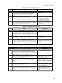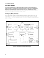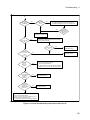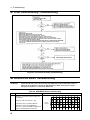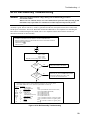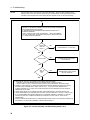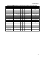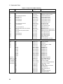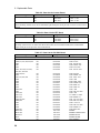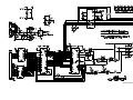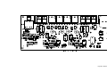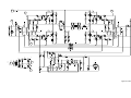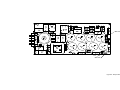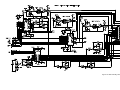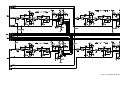
1
Keysight Models 6811A, 6812A, 6813A, 6811B, 6812B, and 6813B AC Power Source/Analyzers Keysight Models 6841A and 6842A Harmonic/Flicker Test Systems Service Manual Warranty Information CERTIFICATION Keysight Technologies certifies that this product met its published specifications at time of shipment from the factory. Keysight Technologies further certifies that its calibration measurements are traceable to the United States National Bureau of Standards, to the extent allowed by the Bureau's calibration facility, and to the calibration facilities of other International Standards Organization members. WARRANTY This Keysight Technologies hardware product is warranted against defects in material and workmanship for a period of three years from date of delivery. Keysight Technologies software and firmware products, which are designated by Keysight Technologies for use with a hardware product and when properly installed on that hardware product, are warranted not to fail to execute their programming instructions due to defects in material and workmanship for a period of 90 days from date of delivery. During the warranty period Keysight Technologies will, at its option, either repair or replace products which prove to be defective. Keysight Technologies does not warrant that the operation for the software firmware, or hardware shall be uninterrupted or error free. For warranty service, with the exception of warranty options, this product must be returned to a service facility designated by Keysight Technologies. Customer shall prepay shipping charges by (and shall pay all duty and taxes) for products returned to Keysight Technologies. for warranty service. Except for products returned to Customer from another country, Keysight Technologies shall pay for return of products to Customer. Warranty services outside the country of initial purchase are included in Keysight Technologies’ product price, only if Customer pays Keysight Technologies international prices (defined as destination local currency price, or U.S. or Geneva Export price). If Keysight Technologies is unable, within a reasonable time to repair or replace any product to condition as warranted, the Customer shall be entitled to a refund of the purchase price upon return of the product to Keysight Technologies. LIMITATION OF WARRANTY The foregoing warranty shall not apply to defects resulting from improper or inadequate maintenance by the Customer, Customer-supplied software or interfacing, unauthorized modification or misuse, operation outside of the environmental specifications for the product, or improper site preparation and maintenance. NO OTHER WARRANTY IS EXPRESSED OR IMPLIED. KEYSIGHT TECHNOLOGIES. SPECIFICALLY DISCLAIMS THE IMPLIED WARRANTIES OF MERCHANTABILITY AND FITNESS FOR A PARTICULAR PURPOSE. EXCLUSIVE REMEDIES THE REMEDIES PROVIDED HEREIN ARE THE CUSTOMER'S SOLE AND EXCLUSIVE REMEDIES. KEYSIGHT TECHNOLOGIES SHALL NOT BE LIABLE FOR ANY DIRECT, INDIRECT, SPECIAL, INCIDENTAL, OR CONSEQUENTIAL DAMAGES, WHETHER BASED ON CONTRACT, TORT, OR ANY OTHER LEGAL THEORY. ASSISTANCE The above statements apply only to the standard product warranty. Warranty options, extended support contacts, product maintenance agreements and customer assistance agreements are also available. Contact your nearest Keysight Technologies Sales and Service office for further information on Keysight Technologies' full line of Support Programs. 2 Safety Summary GENERAL This is a Safety Class 1 instrument (provided with a terminal for connection to protective earth ground). - OPERATION - BEFORE APPLYING POWER: Verify that the product is set to match the available line voltage, the correct line fuse is installed, and all safety precautions (see below) are taken. Also note the instrument's external markings described under "Safety Symbols" WARNING SHOCK HAZARD, EQUIPMENT DAMAGE, PERSONAL INJURY This product is a high-energy instrument, which means that it converts large amounts of energy during normal operation. This can result in catastrophic component damage (rapid, violent, component disassembly) if certain components fail during operation. When covers are removed, always wear a face shield and ear protection when powering up this instrument. Only repair units in a controlled area with no unprotected personnel present. Servicing instructions are for use by service-trained personnel. To avoid dangerous electrical shock, do not perform any servicing unless you are qualified to do so. Before switching on the instrument, the protective earth terminal of the instrument must be connected to the protective conductor of the (mains) power cord. The mains plug shall be inserted only in an outlet socket that is provided with a protective earth contact. This protective action must not be negated by the use of an extension cord (power cable) that is without a protective conductor (grounding). Grounding one conductor of a twoconductor outlet is not sufficient protection. If this instrument is to be energized via an auto-transformer (for voltage change), make sure the common terminal is connected to the earth terminal of the power source. Any interruption of the protective (grounding) conductor or disconnection of the protective earth terminal will cause a potential shock hazard that could result in personal injury. Whenever it is likely that the protective earth connection has been impaired, this instrument must be made inoperative and be secured against any unintended operation. Only fuses with the required rated current, voltage, and specified type (normal blow, time delay, etc.) should be used. Do not use repaired fuses or short-circuited fuseholders. To do so could cause a shock or fire hazard. Do not operate this instrument in the presence of flammable gases or fumes. Do not install substitute parts or perform any unauthorized modification to the instrument. Some procedures described in this manual are performed with power supplied to the instrument while its protective covers are removed. If contacted, the energy available at many points may result in personal injury. Any adjustment, maintenance, and repair of this instrument while it is opened and under voltage should be avoided as much as possible. When this is unavoidable, such adjustment, maintenance, and repair should be carried out only by a skilled person who is aware of the hazard involved. Capacitors inside this instrument may hold a hazardous charge even if the instrument has been disconnected from its power source. SAFETY SYMBOLS Refer to the table on the following page WARNING The WARNING sign denotes a hazard. It calls attention to a procedure, practice, or the like, which, if not correctly performed or adhered to, could result in personal injury. Do not proceed beyond a WARNING sign until the indicated conditions are fully understood and met. Caution The CAUTION sign denotes a hazard. It calls attention to an operating procedure, or the like, which, if not correctly performed or adhered to, could result in damage to or destruction of part or all of the product. Do not proceed beyond a CAUTION sign until the indicated conditions are fully understood and met. 3 Safety Symbol Definitions Symbol Description Symbol Description Direct current Terminal for Line conductor on permanently installed equipment Alternating current Caution, risk of electric shock Both direct and alternating current Caution, hot surface Three-phase alternating current Caution (refer to accompanying documents) Earth (ground) terminal In position of a bi-stable push control Protective earth (ground) terminal (Intended for connection to external protective conductor.) Out position of a bi-stable push control Frame or chassis terminal On (supply) Terminal for Neutral conductor on permanently installed equipment Off (supply) Terminal is at earth potential (Used for measurement and control circuits designed to be operated with one terminal at earth potential.) Standby (supply) Units with this symbol are not completely disconnected from ac mains when this switch is off. To completely disconnect the unit from ac mains, either disconnect the power cord or have a qualified electrician install an external switch. Notice Keysight Technologies shall not be liable for errors contained herein or for incidental or consequential damages in connection with the furnishing, performance or use of this material. This document contains proprietary information which is protected by copyright. All rights are reserved. No part of this document may be photocopied, reproduced, or translated into another language without the prior written consent of Keysight Technologies. The information contained in this document is subject to change without notice. Copyright 1995, 1997, 2000, 2014 Keysight Technologies Printing History First Edition ............October, 1995 Second Edition ...... ... July, 1997 Third Edition ......... September, 2000 Fourth Edition ......... December, 2014 4 Table of Contents Warranty Information Safety Summary Notice Printing History Table of Contents 2 3 4 4 5 1 INTRODUCTION 7 Organization Safety Considerations Related Documents Revisions Instrument Identification Manual Revisions Firmware Revisions Electrostatic Discharge 7 7 7 8 8 8 8 8 2 PERFORMANCE TESTS 9 Introduction Test Equipment Required Current Monitoring Resistor Constant Voltage Tests Procedures 9 9 10 10 11 3 PRINCIPLES OF OPERATION Introduction General Description A1 Front Panel Assembly A2 GPIB / RS-232 Interface Assembly A3 FET Assembly A4 AC Input Assembly A5 DC Rail Asembly A6 Bias Assembly A7 Inverter Assembly A8 Digital Signal Processing (DSP) Assembly A9 Output / Filter Assembly A10 Control Assembly A11 Trigger ( BNC ) Assembly 17 17 17 17 18 18 18 18 19 19 19 19 20 20 5 4 TROUBLESHOOTING Introduction Test Equipment Required Troubleshooting Hints Power-on Self-test Failures Run-Time Errors Overall Troubleshooting Flowchart A1 Front Panel Assembly Troubleshooting A2 GPIB/RS-232 Board Troubleshooting A3 FET Board Troubleshooting A5 DC Rail Assembly Troubleshooting A6 Bias Assembly Troubleshooting A7 Inverter Assembly Troubleshooting Slow-Start Procedure A8 DSP and A10 Control Assembly Troubleshooting A9 Output/Filter/Relay Assembly Troubleshooting A11 Trigger/BNC Board Troubleshooting Initialization ROM Upgrade Identifying the Firmware Upgrade Procedure Post-repair Calibration Inhibit Calibration Switch Disassembly Procedures List of Required Tools Top Cover ( outer cover ) Removal Inner Top Cover Removal A1 Front Frame / Panel Assembly Removal and Replacement A2 HI-IB / RS 232 Board Removal and Replacement A3 AC FET Assembly Removal and Replacement A4 AC Input Board Removal and Replacement A5 DC Rail Board Removal and Replacement A6 Bias Board Removal and Replacement A7 Inverter Assembly Removal and Replacement A8 DSP Board and A10 Control Board Removal and Replacement A11 Trigger ( BNC ) Board Removal and Replacement A9 Output Board Removal and Replacement 5 REPLACEABLE PARTS LIST Introduction Reading the Tables How to Order Parts 6 DIAGRAMS Introduction General Schematic Notes List of Figures INDEX 6 21 21 21 21 22 22 24 26 26 27 29 31 33 39 38 41 42 44 44 44 44 45 45 46 47 47 47 47 48 48 48 48 49 49 49 50 50 51 51 51 51 63 63 63 64 115 1 Introduction Organization This manual contains information for troubleshooting and repairing to the component level models Keysight 6811A/B, 6812A/B, and 6813A/B Power Source/Analyzers, and models Keysight 6841A and 6842A Harmonic Flicker Test Systems. All models will hereafter be referred to as the ac source. This manual is organized as follows: Introduction Chapter 1 Performance tests Chapter 2 Principles of operation on a block-diagram level Chapter 3 Troubleshooting Chapter 4 Replaceable parts Chapter 5 Diagrams Chapter 6 Safety Considerations This ac power source is a Safety Class I instrument, which means it has a protective earth terminal. This terminal must be connected to earth ground through a power source equipped with a 4-wire (3-wire for Keysight 6811A/B), ground receptacle. Refer to the "Safety Summary" page at the beginning of this manual for general safety information. Before operation or repair, check the ac source and review this manual for safety warnings and instructions. Safety warnings for specific procedures are located at appropriate places in the manual. WARNING: SHOCK HAZARD, EQUIPMENT DAMAGE, PERSONAL INJURY - Hazardous voltages exist within the ac power source chassis, at the output terminals, and at the analog programming terminals. Only qualified personnel who have been trained in working with high voltage power equipment are to service this unit. This product is a high-energy instrument, which means that it converts large amounts of energy during normal operation. This can result in catastrophic component damage (rapid, violent, component disassembly) if certain components fail during operation. When covers are removed, always wear a face shield and ear protection when powering up this instrument. Only repair units in a controlled area with no unprotected personnel present. Related Documents The following documents are shipped with your ac source: a Quick-Start Guide, to help you quickly get started using the ac source a User's Guide, containing detailed installation, checkout, and front panel information a Programming Guide, containing detailed GPIB programming information a Quick Reference Card, designed as a memory jogger for the experienced user 7 1 - Introduction Revisions Instrument Identification The ac source is identified by a 10-digit serial number. The items in this serial number are explained as follows: US The first two letters indicates the country of manufacture, where US = USA. 3729 This is a code that identifies either the date of manufacture, or the date of a significant design change. 0101 The last four digits are a unique number assigned to each unit. Manual Revisions This manual was written for ac sources that have the same or higher serial numbers as those listed on the title page. NOTE: If the serial number of your unit is higher than that shown on the title page, your unit was made after the publication of this manual and may have hardware or firmware differences not covered in this manual. If they are significant to the operation and/or servicing of the ac source, those differences are documented in one or more Manual Change sheets included with this manual. If the serial number of your unit is lower than those shown on the title page, your unit was made before the publication of this manual and can be different from that described here. The previous versions of this manual (print date October, 1995 or July, 1997) applies to these units. Firmware Revisions You can obtain the firmware revision number by either reading the integrated circuit label, or query the ac source using the GPIB *IDN?' query command (see Chapter 4, Troubleshooting). Electrostatic Discharge CAUTION: The ac source has components that can be damaged by ESD (electrostatic discharge). Failure to observe standard antistatic practices can result in serious degradation of performance, even when an actual failure does not occur. When working on the ac source, observe all standard, antistatic work practices. These include, but are not limited to: Working at a static-free station such as a table covered with static-dissipative laminate or with a conductive table mat (Keysight P/N 9300-0797, or equivalent). Using a conductive wrist strap, such as Keysight P/N 9300-0969 or 9300-0970. Grounding all metal equipment at the station to a single common ground. Connecting low-impedance test equipment to static-sensitive components only when those components have power applied to them. Removing power from the ac source before removing or installing printed circuit boards. 8 2 Performance Tests Introduction This chapter provides test procedures for checking the operation of a model Keysight 6811AB, 6812A/B, 6813A/B AC Power Source/Analyzer and Keysight 6841A, 6842A Harmonic/Flicker Test System. The required test equipment is specified and sample performance test record sheets are included. Instructions are given for performing the tests using the front panel keypad. Test Equipment Required Table 2-1 lists the equipment required to perform the performance tests in this chapter. A test record sheet with specification limits and measurement uncertainties (when test using the recommended test equipment) may be found at the back of this section. WARNING: SHOCK HAZARD. These tests should only be performed by qualified personnel. During the performance of these tests, hazardous voltages may be present at the output of the unit. Table 2-1. Test Equipment Required for Verification and Performance Tests Type Specifications Recommended Model Digital Voltmeter Resolution: 10 nV @ 1V Readout: 8 1/2 digits Accuracy: 20 ppm Keysight 3458A Current Monitor 0.01 ohms +/-200 ppm 10 Watts Guildline 7320/15 Audio Analyzer Input Voltage: 50mV TO 300V Keysight 8903A Distortion Accuracy: +/-1db 20Hz to 20khz Residual Distortion/Noise: -80db (0.01%) 20Hz to 20kHz Frequency Counter Ratio Transformer 1 Accuracy @1 KHZ < 0.001% Keysight 5316B 30:1 ratio < 50 ppm Variable-Voltage Transformer Power: 1 Phase 3.4KVA Range: 104-127V 47-63 Hz / 207-253V 47-63 Hz Load Resistors 20 ohms, 5 A, 1000 W minimum 250 ohms, 2 A, 500 W minimum 120 ohms, 2.5 A, 750 W minimum 51 ohms, 6 A, 1800 W minimum GPIB Controller Full GPIB capabilities Superior Powerstat HP Series 300 or equivalent 1 A ratio transformer is not required for a valid MIL-STD-5622A 4:1 test. The 30:1 ratio transformer is only required when a 4:1 test equipment ratio is desired using the Keysight 3458A voltmeter in the 1000 volt range. 9 2 - Performance Tests Current Monitoring Resistor A 4-terminal current monitoring resistor (current shunt ) listed in Table 2-1 is required to eliminate output current measurement error caused by voltage drops in the load leads and connections. Constant Voltage Tests If more than one meter or a meter and an oscilloscope are used, connect each to the sense terminals by separate leads to avoid mutual coupling effects. Tables 2-2 through 2-8 provide the test procedures for verifying the 6811A/B, 6812A/B, 6813A/B, and the 6841A, 6842A compliance with the specifications given in Appendix A of the User’s Guide. Please refer to the CALIBRATION PROCEDURE or TROUBLESHOOTING if you observe out-of specification performance. The performance test specifications are listed in the Performance Test Records at the end of this chapter. You can record the actual measured values in the columns provided. When performing the load tests select an adequate gauge wire using the procedures given in the User’s Guide for connecting the load. Figure 2-1. Test Setup 10 Performance Tests - 2 Procedures In the following procedures the term "UUT" means "unit under test" which can be either the 6811A/B, 6812A/B, 6813A/B, 6841A, or 6842A AC Source. Table 2-2. Voltage Programming and Readback Accuracy Step Action Normal Result This procedure verifies that the voltage programming / GPIB readback and Front Panel display functions are within specifications. 1 Turn off the UUT and connect DVM and Ratio Transformer as shown in Test Setup Figure 2-1. Switch S1is open. 2 Turn on the UUT. Recall factory defaults with *RST then CV annunciator on program output to VOLT 300, FREQ 45, SHAPE:SIN Output current near zero 3 Record voltage readings at DMM and on front panel display. Reading within specified high range 300V / 45Hz limits 4 Program FREQ 400 5 Record voltage readings at DMM and on front panel display. 6 Program FREQ 1000, CURR:PEAK 40 7 Record voltage readings at DMM and on front panel display. Reading within specified high range 300V / 400Hz limits Reading within specified high range 300V / 1KHz limits Table 2-3. Constant Voltage Load Effect Step Action Normal Result This test measures the change in output voltage resulting from a change in output current from full-load to no-load or no-load to full-load. 1 Turn off the UUT and connect DMM, Load Resistors, Current shunt and Ratio Transformer as shown in Test Setup Figure 2-1 with S1 closed. 2 Turn on the UUT. Recall factory defaults with *RST. Set CV annunciator on, output current near: 1.2 amps for 6811A/B ALC:DET RMS to rms then program output to VOLT 2.5 amps for 6812A/B 300, FREQ 60, SHAPE:SIN 5.8 amps for 6813A/B 3 Record voltage reading of DMM. 4 Open S1 5 Record voltage readings at DMM. 6 Check test results Output current near zero. The difference between the DMM readings in Step 3 & 5 are within specified load effect limits. 11 2 - Performance Tests Table 2-4. Constant Voltage Source Effect Step Action Normal Result This test measures the change in output voltage resulting from a change in AC Mains Input voltage from minimum to maximum value within the line voltage specification. 1 Turn off the UUT and connect DMM, Load Resistors, Current shunt and Ratio Transformer as shown in Test Setup Figure 2-1 with S1 closed. 2 Connect UUT AC input through a variable voltage transformer 3 Turn on the UUT. Recall factory defaults with *RST. Set CV annunciator on, output current near: 1.2 amps for 6811A/B ALC:DET RMS to rms then program output to 2.5 amps for 6812A/B, 6841A VOLT 300, FREQ 60, SHAPE:SIN, 5.9 amps for 6813A/B, 6842A 4 Adjust variable voltage transformer to low line condition ( 104 or 207 VAC ) 5 Record voltage reading of DMM. 6 Adjust variable voltage transformer to high line condition ( 127 or 253 VAC ) 7 Record voltage readings at DMM. 8 Check test results The difference between the DMM readings in Step 3 & 5 are within specified line effect limits. Table 2-5. RMS Current Accuracy Test Step Action Normal Result This test verifies the measurement accuracy of the rms current readback. 12 1 Turn off the UUT and connect an 20 ohm Load Resistor, current shunt and DMM as shown in Test Setup Figure 2-1 with S1 closed. 2 Turn on the UUT. Recall factory defaults with *RST. Set ALC:DET RMS to rms and then program output voltage to VOLT 60, FREQ 60 SHAPE:SIN, CURR 2.50 for 6811A/B; VOLT 120, FREQ 60 SHAPE:SIN, CURR 5.00 for the 6812A/B, 6813A/B, 6841A, 6842A CC annunciator on, output current near 2.5 amps for 6811A/B - near 5 amps for the 6812A/B, 6813A/B, 6841A, 6842A 3 Record DVM reading and calculate rms current Readings are within specified current high range limits. 4 Program CURR:RANGE LOW CC annunciator on, output current near 2.5 or 5.0 amps 5 Record DVM reading and calculate rms current Readings are within specified current low range limits. Performance Tests - 2 Table 2-6. Harmonic Distortion Test Step Action Normal Result This test measures the total harmonic distortion of the output sinewave at full power 1 Turn off the UUT. Connect load resistor and DMM as shown in Test Setup Figure 2-1 with S1 closed. 2 Turn on the UUT. Program output voltage to VOLT 300, FREQ 60, SHAPE:SIN, CURR MAX 3 CV annunciator on, Output current at 1.2 amps for 6811A/B 2.5 amps for 6812A/B, 6841A 5.8 amps for 6813A/B, 6842A Record the total harmonic distortion reading from the audio Readings are less then maximum analyzer and front panel display of UUT. specified limits. Table 2-7. Frequency Accuracy Test Step Action Normal Result This test verifies the frequency programming and measurement accuracy of the output voltage waveform. 1 Turn off the UUT. Connect the audio analyzer directly to the UUT output terminals. Connect the frequency counter to the Monitor Output on the rear panel of the audio analyzer. 2 Turn on the UUT. Program output voltage to CV annunciator on. VOLT 100, FREQ 400, SHAPE:SIN, CURR MAX 3 Select AC Level on the audio analyzer. Record the output frequency reading from counter and front panel display of UUT. Readings are within specified limits @ 400Hz. Table 2-8. DC Voltage Programming and Readback Accuracy Step Action Normal Result This test verifies the DC voltage programming and front panel readback functions are within specifications. 1 Turn off the UUT. Connect DVM directly to the output terminals. DVM negative lead is connected to COM output terminal. Disconnect the 30:1 transformer. Open S1. 2 Turn on UUT. Program output voltage to VOLT 0, OUTP:COUP DC, OFFSET 425 Output voltage at +425 Vdc, output current near zero. 3 Record dc voltage at DVM and readback from front panel display. Readings within specified dc voltage programming and readback limits. 4 Program output voltage OFFSET -425 Output voltage at -425 Vdc, output current near zero. 5 Record dc voltage at DVM and readback from front panel display. Readings within specified DC voltage programming and readback limits. 13 2 - Performance Tests Table 2-9. Performance Test Record - Keysight 6811A/B Model Report No: Test Description Date: Minimum Specification Results Maximum Specification Meas. Uncert. 300.750 140mV Voltage Programming & Readback Accuracy 300Vrms @ 45Hz 299.250 ________ V Front Panel Display Vrms -190mV ________ V 300Vrms @ 400Hz 298.200 ________ V Front Panel Display Vrms -400mV ________ V 300Vrms @ 1KHz 296.700 ________ V Front Panel Display Vrms -700mV ________ V Vrms +700mV CV Load Effect Vout - 1.5V ________ V Vout + 1.5V CV Line Effect Vout - 0.3V ________ V Vout + 0.3V Vrms +190mV 301.800 Vrms +400mV 303.300 (1.2mV) 140mV (1.2mV) 140mV (1.2mV) rms Current Readback Front Panel Display High Range (A models) Io-0.0175A _______A Io+0.0175A 1mA Front Panel Display Low Range (A models) Io-0.0045A _______A Io+0.0045A 1mA Front Panel Display High Range (B models) Io-0.01125A _______A Io+0.01125A 1mA Front Panel Display Low Range (B models) Io-0.00275A _______A Io+0.00275A 1mA Total Harmonic Distortion Audio Analyzer 0 ________ % 1% Front Panel Display 0 ________ % 1% Frequency Programming & Readback Accuracy Program 400 Hz Front Panel Display 399.960 Hz _______ Hz 400.040 Hz Fo - 0.040 Hz _______ Hz Fo + 0.040 Hz 0.005Hz DC Voltage Programming & Readback Accuracy +425 VDC Output 424.075 Vdc ________Vdc 425.925 Vdc Front Panel Display Vo-0.363 Vdc ________Vdc Vo+0.363Vdc -425 VDC Output -424.075 Vdc ________Vdc 425.925 Vdc Front panel Display Vo-0.363 Vdc ________Vdc Vo+0.363 Vdc 4.4mV 4.4mV Note: 1. Measurement uncertainties are only valid when using test equipment listed in Table 2-1. 2. Voltage Programming and Readback measurement uncertainties are for a 3458A DMM in the 1000 volt range. 3. Measurement uncertainties in parenthesis are only if a 30:1 ratio transformer is used with the 3458A DMM. 14 Performance Tests - 2 Table 2-10. Performance Test Record - Keysight 6812A/B, 6841A Model Report No: Test Description Date: Minimum Specification Results Maximum Specification Meas. Uncert. 300.750 140mV Voltage Programming & Readback Accuracy 300Vrms @ 45Hz 299.250 ________ V Front Panel Display Vrms -190mV ________ V 300Vrms @ 400Hz 298.200 ________ V Front Panel Display Vrms -400mV ________ V 300Vrms @ 1KHz 296.700 ________ V Front Panel Display Vrms -700mV ________ V Vrms +700mV CV Load Effect Vout - 1.5V ________ V Vout + 1.5V CV Line Effect Vout - 0.3V ________ V Vout + 0.3V Vrms +190mV 301.800 Vrms +400mV 303.300 (1.2mV) 140mV (1.2mV) 140mV (1.2mV) rms Current Readback Front Panel Display High Range (A models) Io-0.0175A _______A Io+0.0175A 1mA Front Panel Display Low Range (A models) Io-0.0045A _______A Io+0.0045A 1mA Front Panel Display High Range (B models) Io-0.0125A _______A Io+0.0125A 1mA Front Panel Display Low Range (B models) Io-0.0040A _______A Io+0.0040A 1mA Total Harmonic Distortion Audio Analyzer 0 ________ % 1% Front Panel Display 0 ________ % 1% Frequency Programming & Readback Accuracy Program 400 Hz Front Panel Display 399.960 Hz _______ Hz 400.040 Hz Fo - 0.040 Hz _______ Hz Fo + 0.040 Hz 0.005Hz DC Voltage Programming & Readback Accuracy +425 VDC Output 424.075 Vdc ________Vdc 425.925 Vdc Front Panel Display Vo-0.363 Vdc ________Vdc Vo+0.363Vdc -425 VDC Output -424.075 Vdc ________Vdc 425.925 Vdc Front panel Display Vo-0.363 Vdc ________Vdc Vo+0.363 Vdc 4.4mV 4.4mV Note: 1. Measurement uncertainties are only valid when using test equipment listed in Table 2-1. 2. Voltage Programming and Readback measurement uncertainties are for a 3458A DMM in the 1000 volt range. 3. Measurement uncertainties in parenthesis are only if a 30:1 ratio transformer is used with the 3458A DMM. 15 2 - Performance Tests Table 2-11. Performance Test Record - Keysight 6813A/B, 6842A Model Report No: Test Description Date: Minimum Specification Results Maximum Specification Meas. Uncert. 300.750 140mV Voltage Programming & Readback Accuracy 300Vrms @ 45Hz 299.250 ________ V Front Panel Display Vrms -190mV ________ V 300Vrms @ 400Hz 298.200 ________ V Front Panel Display Vrms -400mV ________ V 300Vrms @ 1KHz 296.700 ________ V Front Panel Display Vrms -700mV ________ V Vrms +700mV CV Load Effect Vout - 1.5V ________ V Vout + 1.5V CV Line Effect Vout - 0.3V ________ V Vout + 0.3V Vrms +190mV 301.800 Vrms +400mV 303.300 (1.2mV) 140mV (1.2mV) 140mV (1.2mV) rms Current Readback Front Panel Display High Range (A models) Io-0.0175A _______A Io+0.0175A 1mA Front Panel Display Low Range (A models) Io-0.0045A _______A Io+0.0045A 1mA Front Panel Display High Range (B models) Io-0.0125A _______A Io+0.0125A 1mA Front Panel Display Low Range (B models) Io-0.0040A _______A Io+0.0040A 1mA Total Harmonic Distortion Audio Analyzer 0 ________ % 1% Front Panel Display 0 ________ % 1% Frequency Programming & Readback Accuracy Program 400 Hz Front Panel Display 399.960 Hz _______ Hz 400.040 Hz Fo - 0.040 Hz _______ Hz Fo + 0.040 Hz 0.005Hz DC Voltage Programming & Readback Accuracy +425 VDC Output 422.575 Vdc ________Vdc 427.425 Vdc Front Panel Display Vo-0.363 Vdc ________Vdc Vo+0.363Vdc -425 VDC Output -422.575 Vdc ________Vdc 427.425 Vdc Front panel Display Vo-0.363 Vdc ________Vdc Vo+0.363 Vdc 4.4mV 4.4mV Note: 1. Measurement uncertainties are only valid when using test equipment listed in Table 2-1. 2. Voltage Programming and Readback measurement uncertainties are for a 3458A DMM in the 1000 volt range. 3. Measurement uncertainties in parenthesis are only if a 30:1 ratio transformer is used with the 3458A DMM. 16 3 Principles of Operation Introduction Figure 3-1 at the end of this chapter is a block diagram showing the major circuits within the AC Power Source /Analyzer and Harmonic / Flicker Test System. These units consist of the following modules. A1 Front Panel Assembly A2 GPIB Assembly A3 AC FET Assembly A4 AC Input Assembly A5 DC Rail Assembly A6 Bias Assembly A7 Inverter Assembly A8 DSP Assembly A9 Output Filter Assembly A10 Control Assembly A11 Trigger Assembly General Description The 6811A/B, 6812A/B, and 6813A/B are 375VA, 750VA and 1750VA AC Source/Analyzers whereas the 6841A and 6842A are 750VA and 1750VA power sources are used as Harmonic / Flicker Test Systems. The 6811A/B, 6812A/B and 6841A can operate from 120, 220 or 240 volt AC input main while the 6813A/B and 6842A only operate from 220/240 volt AC input mains. All deliver regulated AC voltage and/or current from 45 to 1000 hertz. They can operate below 45 hertz to DC at derated output power. (See Users Guide for operation below 45 hertz ). They can generate sine, square, clipped sine or arbitrary waveforms. The output waveform can be controlled from the front panel keypad or computer via GPIB or RS-232. The output characteristics or measurements ( voltage, current, frequency, power factor, etc. ) can be readback via the front panel, GPIB or RS-232. A1 Front Panel Assembly The A1 Intelligent Front Panel assembly contains a circuit board, a vacuum florescent display assembly, keypad and rotary pulse generators ( RPG ). The circuit board contains digital logic circuits including a CPU, ROM and RAM. The front panel CPU decodes operator keystrokes and transmits the information to the A8 DSP assembly. The front panel receives information from the A8 DSP assembly to update the display. The front panel assembly is a surface mount ( SMT ) assembly and is not component level repairable. The A1 front panel assembly is common to all models. 17 3 - Principles of Operation A2 GPIB / RS-232 Interface Assembly The A2 GPIB / RS-232 interface assembly contains the CPU and GPIB interface controller for communicating with a GPIB controller. The A2 interface assembly also contains the logic for communicating with a computer via RS232. The interface type, GPIB or RS-232, is determined by the operator using front panel keystrokes. When using the RS-232 interface the operator can select the baud rate and parity using the front panel keypad. The GPIB / RS232 interface assembly is an SMT assembly and is not component level repairable. The A2 assembly is common to all models. A3 FET Assembly The 6813A/B and 6842A A3 FET assembly contains 8 power FETs and 2 bridge driver ICs. The power FETS and power transformer form an H-Bridge converter. The A3 FET H-Bridge converts the 320 volt DC rail from the AC Input assembly to 500 volts DC on the A9 Output assembly via the A5 DC Rail assembly. The A3 assembly power FETs switching frequency is synchronized with the switching frequency of the A7 Inverter assembly. The A3 FET switching frequency is approximately 42 KHz, 1/2 that of the A7 Inverter assembly. The 6811A/B, 6812A/B and 6842A ACFET assemblies, having lower output power ratings then the 6813A/B and 6842A/B , use only 4 power FETs in the H-Bridge. Earlier ac source models used through-hole FET assemblies. Updated surface-mount FET assemblies (refer to the parts list) are the recommended replacement part for all previous version FET assemblies. The surface-mount FET assemblies are not component-level repairable. The 6811A/B, 6812A/B and 6841A use one common assembly, the 6813A and 6842A use a different unique assembly . A4 AC Input Assembly The AC input mains voltage is connected on the rear panel via J1049 to the A4 AC Input board. The AC input board converts the AC mains to a nominal 320 volt DC rail for use by the AC FET assembly. Relays K1040 and K1041 prevent the DC rail from energizing until the front panel on/off switch closed. Resistors R1040, R1041, R1045 and R1046 limit turn-on surge current to the input filter capacitors C1060 thru C1067. Relay K1040 bypasses the current limit resistors when energized. Relay K1040 is controlled by FET Q1040 who is driven by the input_rly_iso signal derived from the DSP assembly. Wire jumper J1047 connects the full wave bridge rectifier D1060 and input capacitors C1060 thru C1067 as either a voltage doubler for 120 volt mains or full wave bridge for 220/240 volt mains. Fuse F1020 is the main AC line fuse and F1080 protects the 320 volt DC rail to the AC FET assembly. The A4 assembly is component level repairable and there are 3 unique assemblies. One for the 6811A/B, another for the 6812A/B and 6841A and another for the 6813A/B and 6842A. A5 DC Rail Assembly The A5 DC Rail assembly contains U447 the CV error amplifier, U491 PWM driver, U462 PWM comparator and U475 ramp generator to control the FET H-bridge on the A3 ACFET assembly. The chassis mounted power transformer connects the 42 KHz AC from the A3 ACFET assembly to input rectifiers D400 thru D407 on the A5 DC Rail board. Chassis mounted rail filter 5080-2329 and capacitors C500 to C503 and C508 to C509 located on the A9 Output Filter board convert the 42 KHz AC to a 503 volt DC rail for use by the A7 Inverter assembly. It also contains U423 bias voltage detector and high/low 503 volt rail voltage detection circuit. There is a red LED on the right side of the A5 DC Rail assembly to warn when high voltages are present, this LED can be seen from the right side of the AC Source without removing any covers. This assembly is component level repairable but extreme caution must be used when troubleshooting as 1100 volts peak / 503VDC is present. The A5 DC Rail assembly is common to all models. 18 Principles of Operation - 3 A6 Bias Assembly The A6 Bias assembly receives the AC input mains voltage via connector J1035 from the A4AC Input assembly. The bias transformer primaries for models 6811A/B, 6812A/B, or 6841A can be configured for either 100, 120 , 200 or 230 volt nominal input and models 6813A/B and 6842A can only be configured for 200 or 230 volt nominal inputs. The input voltage range is configured by moving jumpers on J353. A J353 jumper configuration diagram is located on the bias assembly next to J353. Regulator U300 supplies +15 volts to the AC input relays and bias to the ACFET assembly. Regulators U311 and U3121 supply +5 volts to the GPIB and front panel assemblies. Opto-coupler U362 transmits the input_rly_iso signal to relay K1040 on the AC input assembly. J337 supplies +5 and +/- 15 volts to the control assembly via the Output Filter assembly and 48 volts AC via E336 to the DC rail assembly. The A6 assembly is a component level repairable assembly. There is one unique assembly for the 6811A/B, 6812A/B and 6841A and another unique assembly for the 6813A/B and 6842A. A7 Inverter Assembly The A7 Inverter (output amplifier ) assembly is a switching H-bridge FET assembly operating at approximately 83 KHz. It receives its switching logic from the A10 control assembly. The A7 Inverter assembly can provide a sine, square, clipped sine, arbitrary waveform or DC level to the A9 Output Filter assembly. The Keysight 6813A/B and 6842A uses twice as many power FETs as the Keysight 6811A/B, 6812A/B and 6841A assembly. Slow start procedures, disconnecting the 503 volt DC rail, should be used when troubleshooting the Inverter assembly. See Inverter troubleshooting for more complete information on slow start procedures. Earlier ac source models used a through-hole inverter assembly. An updated surface-mount inverter assembly (refer to the parts list) is the recommended replacement part for all previous version ac source inverter assemblies. The surface-mount inverter assembly is not component-level repairable. A8 Digital Signal Processing (DSP) Assembly The A8 DSP assembly contains the CPU, ROMs, Digital-to Analog ( DACs ) circuits that control the output voltage and output current settings. It contains Analog-to-Digital ( ADCs ) circuits to readback actual output voltage and current. It contains all logic circuits for generating arbitrary waveforms, frequency changes and transient or pulse level changes. At power on the A8 DSP assembly performs a self test and reports any failures via the front panel display. The A8 assembly is an SMT assembly and is not component level repairable except for the ROMs which are installed in sockets and are replaceable for ROM upgrades. There is one unique assembly for models 6811A/B, 6812A/B, and 6813A/B and another unique assembly for models 6841A and 6842A. A9 Output / Filter Assembly The A9 Output filter assembly contains U500 the remote sense amplifier and K501 remote sense relay. The rms and peak current sense resistors, overvoltage divider and output disconnect relays K502 and K503 ( older manufactured units use one output disconnect relay K500 ). The A9 Output assembly contains 2 notch filters to reduce the inverter switching frequency noise in the output. It provides a communication path between the A10 Control assembly, A5 DC rail assembly and A6 Bias assembly. The A9 assembly is component level repairable. There is one unique assembly for model 6811A/B and another unique assembly for models 6812A/B, 6813A/B, 6841A and 6842A. 19 3 - Principles of Operation A10 Control Assembly The A10 Control assembly contains the PWM comparator and ramp generator for controlling the A7 Inverter assembly power FETs. It contains the voltage and current rms/dc converter circuits, voltage and current readback amplifiers and all other analog circuits required to interface the output voltage , output current and frequency programming and measurement capabilities with the A8 DSP assembly. The A10 assembly is an SMT assembly and is not component lever repairable. There are three unique A10 Control assemblies, one for model 6811A/B, one for models 6812A/B, and 6841A and one for models 6813A/B, and 6842A. A11 Trigger ( BNC ) Assembly The A11 Trigger or BNC assembly provides the communication and isolation path for trigger out ( U157 ) and trigger in signals ( U156 ). The A11 assembly provides the isolation ( optical couplers ) between the A2 GPIB interface assembly ( U153 & U154 ) and A8 DSP assembly ( J115 ). The A11 assembly is an SMT assembly and is common to all models. Figure 3-1. AC Power Source/Analyzer Block Diagram 20 4 Troubleshooting Introduction WARNING: SHOCK HAZARD, EQUIPMENT DAMAGE, PERSONAL INJURY - Some troubleshooting procedures in this chapter are performed with power applied and protective covers removed. These procedures should be performed only by trained personnel who are aware of the hazards. This product is a high-energy instrument, which means that it converts large amounts of energy during normal operation. This can result in catastrophic component damage (rapid, violent, component disassembly) if certain components fail during operation. When covers are removed, always wear a face shield and ear protection when powering up this instrument. Only repair units in a controlled area with no unprotected personnel present. CAUTION: This instrument uses components which can either be damaged or suffer serious performance degradation as a result of ESD (electrostatic discharge). Observe the standard antistatic precautions to avoid damage to the components. An ESD summary is given in Chapter 1. This chapter provides troubleshooting and repair information for the AC Power Source. Before beginning troubleshooting procedures make certain the problem is in the AC Power Source and not with an associated circuit , the GPIB controller or AC input lines. Without removing the covers you can use the verification tests in Chapter 2 to determine if the AC Power Source is operating normally. Test Equipment Required Equipment GPIB Controller Digital Voltmeter Function Generator Oscilloscope Current Shunt Logic Probe Table 4-1. Test Equipment Requirements for Troubleshooting Characteristics Recommended Model Communicate with AC Source via GPIB or RS232 HP Series 200/300 controller or equiv. Check voltages /resistances Keysight 3458A or equivalent Generate waveforms Keysight 3312A or equivalent Observe waveforms Keysight 54504A or equivalent Check output current 0.01 ohm 10 watt Check data lines Keysight 545A or equivalent Troubleshooting Hints Service kit 5063-2330 contains 2 PC board holders to hold the A5 DC Rail board in a vertical position for troubleshooting, and a PC board extender that raises the A8 DSP and A10 Control boards above the chassis for troubleshooting. Extender board part number 5063-2331 PC B holder part number 5020-8458 Locate and observe the 2 red LEDs, one on each side of the unit, which indicate when high voltage is present on the A4 AC input board, A5 DC rail board, and A9 output board. Wait for the LEDs to extinguish before removing or installing assemblies. If both CV and CC annunciators are on, the peak current limit is may be set too low. 21 4 - Troubleshooting Power-on Self-test Failures The power-on self-test sequence tests of most of the digital and DAC circuits. If the supply fails self-test, the display "ERR" annunciator will come on. You can then query the unit to find out what the error(s) are. When an error is detected, the output is not disabled so you can still attempt to program the supply to help troubleshoot the unit. Table 4-2 lists the self test errors and gives a possible remedy for each error. Table 4-3 lists the run-time errors that can occur at any time while the unit is running. NOTE: A partial self test is performed when the *TST? query is executed. Those tests that interfere with normal interface operation or cause the output to change are not performed by *TST?. The return value of *TST? will be zero if all tests pass, or the error code of the first test that failed. The power supply will continue normal operation if *TST? returns a non-zero value. Table 4-2. Self-Test Errors Error # Description 0 No error - 1 Non-volatile RAM RD0 section checksum failed A 2 Non-volatile RAM CONFIG section checksum failed A 3 Non-volatile RAM CAL section checksum failed A 4 Non-volatile RAM WAVEFORM section checksum failed A 5 Non-volatile RAM STATE section checksum failed A 6 Non-volatile RAM LIST section checksum failed A 7 Non-volatile RAM RST section checksum failed A 10 RAM selftest B 11 - 31 DAC selftest error, expected <n>, read <reading> Errors 11, 12, 13, 14, 15 apply to DAC12 1A and 1B Errors 16, 17, 18 apply to DAC12 2A Errors 19, 20, 21 apply to DAC12 2B Errors 22, 23 apply to DAC12 4A Errors 24, 25 apply to DAC12 4B Errors 26, 27, 28 apply to DAC12 3A and 3B Errors 29, 30, 31 apply to DAC12 5A and 5B B 40 Voltage selftest error C 43 Current selftest error C 70 Fan voltage failure D 80 Digital I/O selftest error D A Re-initialize unit and re-calibrate. If unit still has RAM error replace A8 DSP board. B Check A8 DSP and A10 Control assemblies C *TST? programs 50 volts, expected readback 50+/-1volt 0+/-1amp D Check fan and/or fan voltage or replace A8 DSP assembly. Possible Remedy Run-Time Errors Run-time errors do not occur during self-test, but can occur at any time while the unit is running. (See Table 4-3). 22 Troubleshooting - 4 Table 4-3. Run-Time Errors Error # 200 201 210 211 212 213 214 215 216 217 218 219 220 221 222 223 224 401 402 403 404 405 406 600 601 602 603 604 605 606 607 608 609 610 Description Outgrd not responding Front panel not responding Ingrd receiver framing error Ingrd uart overrun status Ingrd received bad token Ingrd receiver buffer overrun Ingrd input buffer overrun Outgrd output buffer overrun RS-232 receiver framing error RS-232 receiver parity error RS-232 receiver overrun error Ingrd inbuf count sync error Front panel uart overrun Front panel uart framing Front panel uart parity Front panel buffer overrun Front panel timeout CAL switch prevents calibration CAL password is incorrect CAL not enabled Computed readback cal constants are incorrect Computed programming cal constants are incorrect Incorrect sequence of calibration commands Systems in mode:list have different list lengths Requested voltage and waveform exceeds peak voltage capability Requested voltage and waveform exceeds transformer volt-second rating Command only applies to RS-232 interface Trigger received before requested number of pre-trigger readings Requested RMS current too high for voltage range Waveform data not defined VOLT, VOLT:SLEW, and FUNC:SHAP modes incompatible Measurement overrange Output buffer overrun Command cannot be given with present SYST:CONF setting E Communication error between A1 GPIB, A8 DSP and/or A11 trigger assemblies. F Communication error between A3 front panel, A8 DSP and /or A11 Trigger assemblies. G RS-232 communication or programming error. H Check CAL switch positions (see Figure 4-11). J See Appendix B in User’s Guide for calibration procedure. K Programming error (see applicable programming command in Programming Guide). Possible Remedy E F E E E E E E G G G E F F F F F H H J J J J K K K K K K K K K K K 23 4 - Troubleshooting Overall Troubleshooting Flowchart Figure 4-1 gives the overall procedures to isolate a fault to a circuit board or particular circuit. See Figure 6-1 for the location of the circuit boards. START TROUBLESHOOTING PROCEDURES TURN UNIT OFF. DISCONNECT LOAD. DO NOT REMOVE OUTER COVER (TORX T25) AND INNER COVER (TORX T15/T20) UNLESS REQUIRED BY THE PROCEDURE. WEAR A FACE SHIELD AND EAR PROTECTION WHENEVER THE COVERS ARE REMOVED. TURN UNIT ON. CHECK FOR ANY INDICATION AC POWER ON. IS AC INPUT ASSY LED ON ? note 1 SEE FIGURES 6-8 AND 6-9. CHECK FUSE A4F1020 / LINE SWITCH, A4 E1048 CONNECTIONS TO L1050 LINE CHOKE CHECK A4TP1050-2 FOR ~150VDC, +RAIL FOR ~300VDC SEE FIGURES 6-12 & 6-13 CHECK FUSE A6 F300 & A6 F301, +15Vpri & +12Vpri FROM A6 BIAS ASSY TO A4 ACINPUT ASSY NO YES NO IS DISPLAY ON ? NO IS FAN ON ? CHECK FUSE A6F301 LINE VOLTAGE SWITCH A4J353 SETTING SEE A6 BIAS BOARD TROUBLESHOOTING YES YES PRESS SHIFT KEY ON FRONT PANEL SHIFT ANNUNICIATOR LIGHTS ? NO CHECK +5V TO A8 DSP ASSY YES CHECK DRDX / DTXD SIGNALS @ A11 TRIGGER ASSY U150-5 TO D COM J7462-2 ON A8 DSP ASSY U151-1 TO D COM J7462-2 ON A8 DSP ASSY U164-5 TO D COM J7462-2 ON A8 DSP ASSY U163-6 TO H COM J114-2 ON A11 TRIG ASSY CHECK BIAS VOLTAGES ( +5V SEC / -15V ) A6 BIAS / A9 OUTPUT / A8 DSP / A10 CONTROL ASSY GO TO A1 FRONT PANEL TROUBLESHOOTING IS ERROR ANNUNICATOR ON ? YES PRESS [ SHIFT ] [ ERROR ]. SEE TABLE 4-2 FOR SELF-TEST ERROR MESSAGE NO PROGRAM "VOLT 120" "OUTPUT ON" Notes: 1. View LED from lower left side of power supply. "A" Figure 4-1. Overall Troubleshooting Procedures (sheet 1 of 2) 24 Troubleshooting - 4 "A" MEASURE 120 VAC @ OUTPUT TERMINALS YES MEASURED VOLTAGE IS WITHIN SPEC? PROGRAM "OUTPUT OFF" CONNECT LOAD RESISTOR (20 OHMS) AND CURRENT SHUNT ACROSS OUTPUT TERMINALS PROGRAM "OUTPUT ON" "CURRENT 5.00" YES NO NO NO OUTPUT CURRENT @ 5A WITHIN SPEC CC MODE? PERFORM VERIFICATION & CALIBRATION AS REQUIRED IS DC RAIL LED ON? DISCONNECT CABLE FROM A9E527 (OUTPUT BOARD) NO TO J625 (INVERTER BOARD) YES IS YES DC RAIL LED GO TO A7 INVERTER TROUBLESHOOTING ON? NO MEASURE DC RAIL J444-1 TO J444-3 503 +/-4 VDC NO GO TO A3 FET/A5 DC RAIL TROUBLESHOOTING YES MEASURE 120 VAC A9TP501 TO CHECK OUTPUT RELAY A9K500, A9Q501, D501 OUTPUT_RELAY (HI) @ A10J524-45 OUT_RELAY (HI) @ A10J821-22 (IF THESE SIGNALS DO NOT TOGGLE WITH OUTP ON PROBLEM WITH A1 FRONT PANEL OR A8 DSP BOARD YES A9TP502 NO MEASURE ~3.5 Vpp SINEWAVE @ A10J822-5 CONTROL BOARD NO GO TO A8 DSP TROUBLESHOOTING YES CHECK PULSES AT A10U1801-25 CONTROL BOARD SEE FIG 6-18 NO GO TO A10 CONTROL BOARD TROUBLESHOOTING YES IF FAULT IS VOLTAGE OR CURRENT READBACK CHECK OUTPUT AND CONTROL BOARDS IF FAULT IS TRIG IN, TRIG OUT, RI OR DFI GO TO A11 TRIGGER BOARD TROUBLESHOOTING IF FAULT IS NO OUTPUT CHECK A7 INVERTER BOARD Figure 4-1. Overall Troubleshooting Procedures (sheet 2 of 2) 25 4 - Troubleshooting A1 Front Panel Assembly Troubleshooting Figure 4-2. Front Panel Assembly Troubleshooting A2 GPIB/RS-232 Board Troubleshooting WARNING: Step Disable the 500 Vdc rail by disconnecting cable 5080-2365 from A5-J400. Then connect a jumper from A5-J445-4 to A5-J445-10. This disables the RAIL_LOW_FAULT signal. Also place an insulator over the A5 DC Rail board. Table 4-4. GPIB/RS232 Board Troubleshooting Procedure Waveform 1. Check for +5 Vdc at L100 (see Figure 6-5 for location). 2. Check for clock waveform at Y100. 3. Connect the unit to a GPIB or RS232 controller to check the GPIB/RS232 transceivers. Note that GPIB and RS232 use separate communication transceivers. 26 2.00 V/div HP-IB CRYSTAL 50.0 ns/div -250.0 ns Troubleshooting - 4 A3 FET Board Troubleshooting Because test points on the FET board are not accessible when the board is installed, troubleshooting must be performed with the board removed from the power supply. Troubleshooting procedures are provided with both power removed and power applied. The location of different test points are shown by encircled numbers on the A3 FET Board schematic and component location diagrams. NOTE: Step 1 2 3 4 5 6 8 9 10 11 12 13 14 15 16 17 Earlier ac source models used through-hole FET assemblies. Updated surface-mount FET assemblies (refer to the parts list) are the recommended replacement part for all previous version FET assemblies. The surface-mount FET assemblies are not component-level repairable. Table 4-5. FET Board Troubleshooting Procedure Result With all power removed Turn the power supply off and remove the A3 FET board with See Disassembly Procedures its heatsink assembly attached (see Disassembly Procedures). Measure the resistance between the +Rail (E502) and the - Rail Value should be >20 M (E501) and common (-Rail). Measure the resistance between the gate of each FET (Q201Value should be >15 k 204, Q211, Q222, Q233, and Q244) and common (-Rail). Measure the resistance across capacitor C201. Value should be approx. 150 Measure the resistance across the 15 V bias input (E506 to Value should be approx. 1 k in the E507). forward direction and 490 reversed. With signal from external waveform generator applied Short the collectors of Q251 and Q252 by connecting the collector (case) of each transistor to common (E507). Connect a waveform generator to J200-1 and J200-2. Set generator to produce a 20kHz, 20Vp-p triangular waveform. See Figure 4-3A. Connect 15 V from an external supply to E506 (positive) and Value should be approx. 1 k in the E507 (common). forward direction and 490 reversed. Note: All of the following measurements are taken with respect to E507 common (same as TP 26 on A3 FET Board). Check bias voltage at U203-1 (TP 27). +5V While adjusting the external 15 V supply input, check the bias Voltage goes from low of 0V to high of trip point at U204-1 (TP 28). 5V at an input of approx. 12V, and from high to low at an input of approx. 13V Set external supply input to + 15V and check drive 1 waveform See Figure 4-3B. at U201-10 (TP 29), and drive 2 waveform at U201-12 (TP 30). Check that pulses are present at U201-1(TP 31), U201-7 (TP See Figure 4-3C. 32), U202-1 (TP 33), and U202-7 (TP 34) Pulses should be present on both sides of inductors L201-204 and L213-216 as follows: Check the pulses on the driver transistor side (Q251-Q254) of See Figure 4-3D. each inductor. Check the pulses on the FET regulator side (Q201-Q204, See Figure 4-3E. Q211,Q222, Q233, and Q244) of each inductor. If the waveforms do not have the fast step as shown in Figure 4-3, then the associated FET gate input has an open circuit. Measure the VREF voltage at U204-4 (TP 35). approx. 1.7 V. All pulses turned off. Check the peak current limit by connecting a 68 k resistor from +5 V (U201-9) to U204-5. 27 4 - Troubleshooting 5V / DIV 5V / DIV 10 uS / DIV 10 uS / DIV A. J200 TEST SIGNAL FROM SIGNAL GENERATOR 5V / DIV B. U201/U202 PINS 10, 12 DRIVE SIGNAL 5V / DIV 10 uS / DIV C. U201/202 PINS 1, 7 DRIVE SIGNAL 10 uS / DIV D. L201-L204, L213-216 DRIVE SIDE 5V / DIV 10 uS / DIV E. L201-L203, L213-L216 REGULATOR SIDE Figure 4-3. FET Assembly Test Waveforms 28 Troubleshooting - 4 A5 DC Rail Assembly Troubleshooting WARNING: This board contains hazardous voltages during some troubleshooting procedures. Use extreme caution. When covers are removed, always wear a face shield and ear protection when powering up this instrument. Only repair units in a controlled area with no unprotected personnel present. Before troubleshooting the A5 DC Rail board, refer to the previous procedure and determine that the A3 AC FET Assembly is good. The 503 Vdc rail (+/-4Vdc) is generated from the 300 Vac input board rail, the A3 FET board, and the power transformer. The A5 DC Rail board contains the PWM and CV error amplifiers for controlling the FET switches. Troubleshooting the bias, PWM, and CU error amplifiers must be done with the 300 Vdc rail disconnected from the A3 FET assembly. DISCONNECT CABLE FROM A3 FET BOARD TO J1042 ON A4 AC INPUT BOARD. DISCONNECT CABLE FROM A9 OUTPUT BOARD TO J625 ON A7 INVERTER BOARD. REMOVE 5 SCREWS HOLDING A5 DC RAIL BOARD AND HOLD A5 DC RAIL BOARD IN VERTICAL POSITION USING BOARD HOLDERS. JUMPER TP#1 & TP X TURN ON AC INPUT START MEASURE BIAS VOLTAGES: TP404 = COMMON TP401 = +15VDC TP402 = -15VDC TP403 = +5VDC MEASURE +10V RAIL_REF @ C454+ = 10.00VDC PWM_EN NO @ +5V ? CHECK U423 BIAS DETECT CIRCUIT PWM_EN WILL INHIBIT A8 DSP BOARD YES WAVEFORM EXT_CLK_ISO U436-6 OK? NO CHECK EXT_SYNC U436-3 TO X CHECK EXT_CLK_SYNC A10 J824-1 CONTROL BOARD IF SIGNAL NOT PRESENT @ A10 J824-1, THEN A10 CONTROL OR A8 DSP BOARD FAULT YES THE CV ERROR AMPLIFIER, PWM COMPARATOR, PWM DRIVER, RAMP GENERATOR AND HV/LOW RAIL DETECT CIRCUIT CAN BE CHECKED BY APPLYING 0V OR 10V TO RAIL_VMON. CHECK RAMP GENERATOR AT U475-1 AND U475-7 (SEE FIGURES 4-5C AND 4-5D). 0V applied 10V applied CV ERROR AMP -15V +15V PWM COMPARATOR +5V 0 RAIL_OV_INH +5V +5V RAIL_INH_ISO 0 0 RAMP PULSE PULSE PULSE 1/2 EXT_CLK_ISO +5V PULSE PWM DRIVER (disconnected) 0 PULSE PWM DRIVER (normal) PULSE 0 RAIL_OV_INH +5V 0 0 RAIL_LOW_WARN +1.2V 0 LRFIN 5V LRFDEL +5V 0 U447-7 U462-7 U463-3 (LOW WHEN RAIL OVERVOLTAGE IS TRUE) U463-4 (HIGH INHIBITS PWM DRIVER) U463-14 (SEE FIGURE 4-5B) U463-15 (SEE FIGURE 4-5A) U491-8,9 (SEE FIGURE 4-5E) U491-8,9 (SEE FIGURE 4-5F) U424-14 (TOGGLES AT APPROX. 10.6V @ RAIL_VMON) U424-14 (TOGGLES AT APPROX. 9.3V @ RAIL_VMON) U424-1 (TOGGLES AT APPROX. 8.4V @ RAIL_VMON) U433-1 Figure 4-4. DC Rail Assembly Troubleshooting 29 4 - Troubleshooting 2.00 V/div 5.00 us/div 5.00 us/div 1.00 V/div RAMP GENERATOR PULSE R483/R489 TO TP404 EXT_CLK_ISO U436-6 (R459) TO TP404 RAMP PULSE 83 kHz EXTERNAL CLOCK B A 2.00 V/div 5.00 us/div 2.00 V/div 5.00 us/div RAMP GENERATOR U475-7 (R480) TO TP404 RAMP GENERATOR U475-1 (R487) TO TP404 RAMP GENERATOR NO. 2 RAMP GENERATOR NO. 1 D C 5.00 V/div 5.00 V /div 10.00 us/div PWM DRIVER U491-8 TO U491-9 RAIL DISCONNECTED FROM AC FET (PULL J1042 AC INPUT) PWM DRIVER U491-8 TO U491-9 500 V DC RAIL DISCONNECTED FROM INVERTER SHORT RAIL_LO_FAULT TP#1 TO X PWM DRIVER - AC FET RAIL DISCONNECTED PWM DRIVER - NORMAL OPERATION E Figure 4-5. DC Rail Assembly - Test Waveforms 30 5.00 us/div F Troubleshooting - 4 A6 Bias Assembly Troubleshooting Checking the A6 Bias Assembly consists of checking the bias voltages and the fan speed control circuit. WARNING: Disable the 500 Vdc rail by disconnecting cable 5080-2365 from A5-J400. Then connect a jumper from A5-J445-4 to A5-J445-10. This disables the RAIL_LOW_FAULT signal. Also place an insulator over the DC Rail board. NOTE: You can determine if any of the bias voltage regulators are operating in current limit mode by disconnecting the cable going to the circuit where the bias is used. If the bias voltage returns to normal with the cable disconnected, most likely the bias circuit is OK. Step 1 2 3 3 4 Table 4-6. Bias Assembly Troubleshooting Procedure Result Check F301 If open, replace fuse. If fuse blows again, troubleshoot the bias circuits. Check the bias voltages at the following locations. Measure at the indicated points: Test point Common point C314+ and C302- (P) +12 Vdc (+12V PRI to A4 Input board) C304+ and C302- (P) +15 Vdc (+15V PRI to A3 FET board) C313+ and C317- (H) +12 to 15 Vdc (+5V UNREG to U311, U312) U312 tab and C317- (H) +5 Vdc (+5VDC to A1 Front Panel) U311 tab and C317- (H) +5 Vdc (+5V DC to A2 GPIB board) U322 tab and C329+ (Y) +15 Vdc (+15VSEC to A8 DSP, A9 Output, A10 Control boards) C331 tab and C329+ (Y) -15 Vdc (-15VSEC to A8 DSP, A9 Output, A10 Control boards) E346-2 and D322 (F) +25 to 30 Vdc (+25 V UNREG to A7 Inverter, A8 DSP boards) E346-1 and D322 (F) +5 V (+5 V SEC to A7 Inverter, A8 DSP boards) E336-2 and E336-3 ~22 Vac (~22Vac to dc rail bias regulator) E336-1 and E336-3 ~44 Vac (~44Vac to dc rail bias regulator) Check the fan speed supply by measuring the voltage at: Test point Common point C361+ and D322 (F) 4.7 Vdc (in AUTO mode) Change the fan speed and check for the correct voltage as follows: Press 0 and 9 simultaneously. EE INIT <model> Press twice, once, and ENTER FAN:MODE MAN Press 0 and 9 simultaneously. EE INIT <model> Press once. FAN:SPEED <n> Enter a fan speed, then ENTER 10 = 5.7 Vdc 50 = 9.6 Vdc 100 = 14.6 Vdc After the fan speed test, enter the following command: *RST SHIFT OUTPUT ENTER This restores the fan speed to automatic mode. 31 4 - Troubleshooting Figure 4-6. Bias Assembly Voltage Distribution 32 Troubleshooting - 4 A7 Inverter Assembly Troubleshooting WARNING: SHOCK HAZARD, EQUIPMENT DAMAGE, PERSONAL INJURY Failure to first follow the slow-start procedure after replacing the A7 inverter board may result in catastrophic component damage when powering up the instrument. When covers are removed, always wear a face shield and ear protection when powering up this instrument. Only repair units in a controlled area with no unprotected personnel present. NOTE: Earlier ac source models used a through-hole inverter assembly. An updated surface-mount inverter assembly (refer to the parts list) is the recommended replacement part for all previous version ac source inverter assemblies. The surface-mount inverter assembly is not component-level repairable. TURN ON AC SOURCE A 10 U 1801- 23 NO TROUBLESHOOT A8 DSP/ A 10 INV_OFF LOW ? CONTROL ASSEMBLIES SEE FIG 6- 18 YES CHECK FOR PWM SIGNALS AT PWM DRIVE A10 U 1801- 25. SEE FIG 4-8A A 10 U 1801- 25 PWM SIGNAL PRESENT? NO YES TURN UNIT OFF. REMOVE CABLE FROM OUTPUT A7 J625. TURN UNIT ON. CHECK Q 601 THRU Q 608 AND Q 611 THRU Q 618 GATE SIGNALS , SEE FIG 4-8B , 4-8 C. CHECK Q 627 , Q 629 , Q 637 AND Q 639 DRAIN PULSE , SEE FIG 4-8 D. CHECK Q 633 , Q 635 , Q 641 AND Q 643 DRAIN PULSES , SEE FIG 4-8E. ALL WAVEFORMS OK? NO " A" YES A. CONNECT EXTERNAL 30 VDC TO J 627 (+ TO J 627 -1) ( - TO J 627 -2) B. REMOVE CABLE (S) TO J 526 AND J 527 ON A9 OUTPUT BOARD C. CONNECT OSCILLOSCOPE TO J 526 AND OBSERVE WAVEFORM FIG 4-8F D. IF WAVEFORM IS NOT CORRECT, GO TO “A” ON NEXT SHEET E. IF WAVEFORM IS CORRECT CHECK A9 OUTPUT BOARD FILTER Figure 4-7. Inverter Assembly Troubleshooting (sheet 1 of 2) 33 4 - Troubleshooting NOTE: The procedure below references the Slow Start Procedure. This procedure should be used whenever the A7 Inverter board is replaced to prevent destruction of the replacement inverter assembly if the original cause of the failure did not originate on the A7 inverter assembly. "A" REMOVE A7 INVERTER ASSEMBLY CHECK FOR CRACKED OR BROKEN FETS, BURN MARKS ON PC BOARD. IF BROKEN FETS OR BURN MARKS ARE OBSERVED REPLACE A7 INVERTER ASSEMBLY. APPLY +20VDC @ J638-2 AND +5VDC@J638-1. J638-34 IS COMMON. OR USE "SLOW START" PROCEDURE. SEE STEP "E" BELOW AND SEE A7 “SLOW START PROCEDURE”. +12VDC @ U619-2 & U620-2 ? NO TROUBLESHOOT +12 VDC BIAS YES U621-6 LOW ? NO TROUBLESHOOT Q644 & U621 PCLR CIRCUITS YES U607-1 & U609-1 HI ? NO TROUBLESHOOT U602, Q619 & INN_OFF CIRCUITS YES A. USE 8-PIN DIP TEST CLIP TO CONNECT FOLLOWING TEST EQUIPMENT 1. CONNECT FUNCTION GENERATOR 83 KHZ SQUARE WAVE TO U602-3 & U602-4 2. SHORT U602-5 TO U602-7. OPTO MUST BE LOW FOR U608 TO GENERATE TURN-ON PULSES. B. CONNECT OSCILLOSCOPE TO U608-2 AND INCREASE FUNCTION GENERATOR GAIN UNTIL 83KHZ SQUARE WAVE IS OBSERVED AT U608-2. SEE FIG 4-8 G. NOTE; FUNCTION GENERATOR IS CONNECTED DIRECTLY TO U602 OPTO DIODE. BE SURE FUNCTION GENERATOR HAS INTERNAL IMPEDANCE OF 50 OHMS. C. CHECK GATE DRIVE TO ALL POWER FETS Q601 THRU Q608 AND Q611 THR Q618 SEE FIG 4-8H. D. CHECK WAVEFORM AT "H" BRIDGWE OUTPUT E626-1 TO E626-2 AND E627-1 TO E627-2. SEE FIG 4-8H E. IF ALL WAVEFORMS ARE CORRECT REINSTALL A7 INVERTER ASSEMBLY. CONNECT ALL CABLES EXCEPT 503 VDC RAIL. CONNECT EXTERNAL DC SOURCE TO A7J625. SEE A7 “SLOW START PRODEDURE”. F. CHECK CURRENT WAVEFORM FIG 4-8J. PROGRAM AND CHECK OUTPUT VOLTAGE AND CURRENT TO DETERMINE IF A7 INVERTER ASSEMBLY IS OPERATING PROPERLY. Figure 4-7. Inverter Assembly Troubleshooting (sheet 2 of 2) 34 Troubleshooting - 4 1.00 V/div 2.00 V 5.00 us/div 5.00 V/div 0.00 s 0.00 V 2.00 us/div -18.00 us SCOPE DC COUPLED GATE TO -RAIL A10U1801-25 X 0V PWM DRIVE 0V A 5.00 V/div 0.00 V 2.00 us/div B -18.00 us SCOPE DC COUPLED GATE TO -RAIL 5.00 V/div 0.00 V 2.00 us/div -16.00 us SCOPE DC COUPLED DRAIN TO -RAIL 0V 0V C 5.00 V/div 0.00 V 2.00 us/div SCOPE DC COUPLED DRAIN TO -RAIL D 20.00 V/div -16.00 us 0.00 V 2.00 us/div 8.00 us J526 OR J527 EXTERNAL 30 VDC TO J625 OUTPUT ON 0V E F Figure 4-8. Inverter Assembly - Test Waveforms (sheet 1 of 2) 35 4 - Troubleshooting 2.00 V/div 0.00 V 2.00 us/div 5.040 us U608-2 TO 5.00 V/div 2.00 us/div 0.00 V GATE TO 0V G 10.00 V/div 0.00 V 2.00 us/div H 200 mV/div 5.040 us 0.00 V 5.00 us/div 1 mA/mV INVERTER CURRENT EXTERNAL 30 VDC TO J625 OUTPUT OFF E626-1/E627-1 TO E626-2/E627-2 EXTERNAL 30 VDC TO J625 I Figure 4-8. Inverter Assembly - Test Waveforms (sheet 2 of 2) 36 5.040 us J -25.00 us Troubleshooting - 4 Slow-Start Procedure WARNING: SHOCK HAZARD, EQUIPMENT DAMAGE, PERSONAL INJURY Failure to first follow the slow-start procedure after replacing the A7 inverter board may result in catastrophic component damage when powering up the instrument. When covers are removed, always wear a face shield and ear protection when powering up this instrument. Only repair units in a controlled area with no unprotected personnel present. The A7 Slow-Start troubleshooting procedure allows testing the A7 inverter assembly and A10 control assembly voltage and current loops using an external DC power supply in place of the AC source 500 Vdc rail. Service Kit 5063-2330 will be required to perform both procedures. 1. Turn off the UUT (AC source ) and remove cable 5080-2698 from A7-J625. This cable disconnects the 500 Vdc rail from the A7 Inverter assembly. WARNING: SHOCK HAZARD. Unless you perform step #2, the 500 Vdc rail will still be present on the A5 dc rail assembly during the slow-start procedure. 2. To disable the 500 Vdc rail during the following tests, disconnect cable 5080-2365 from A5-J400. This will remove the PWM drive to the A3 AC FET assembly and disable the 500 Vdc rail. Then connect a jumper from A5-J445-4 to A5-J445-10. This disables the RAIL_LOW_FAULT signal and allows the DSP assembly to function. 3. Use the extender board from the service kit and raise the A8 DSP and A10 Control assemblies from the unit. Verify that the A8 and A10 assemblies are functioning properly. Refer to the A8 DSP and A10 Control assembly troubleshooting procedures. 4. If the A8 DSP and A10 Control assemblies check good, turn off the unit and re-install the A8 and A10 assemblies in the unit. 5. Using cable 5080-2381 (remove from defective A7 PCA. Or order this cable), connect an external ( 60V/2A minimum ) DC power supply to the A7 Inverter assembly A7-J625. 6. Turn on the unit and DC power supply. 7. Set the external DC supply for 0 volts and 2 amps current limit. 8. Slowly increase the external DC supply voltage to 60 Vdc observing the current from the external supply. The external supply should go to 60 Vdc with only 200 to 300 milliamperes current from the external supply. If the current raises immediately check for shorted FETs on the A7 Inverter assembly. 9. Connect an oscilloscope to the unit's output terminal block. Enable the output. Using the front panel knob, increase the output voltage while observing the oscilloscope. A harmonic free sine wave should appear on the oscilloscope until the output voltage reaches approximately 30-35 volts. At this time the sine wave will develop a flat top. This test verifies the voltage control loop. 10. Disable the output and connect a load resistor ( 20 ohms ) capable of sinking 1.5 to 2 amps to the output terminals of the unit. 11. Enable the output and set CURR:LEV to 1 amp. The unit should current limit at 1 ampere and the CC annunciator should come on. The response of the RMS ( CURR:LEV ) loop is slow so you will have to wait a moment. Set the CURR:LEV to 3 amps and set CURR:PEAK to 1 amp. Both the CV and CC annunciators should come on. These tests verify both the RMS and PEAK current loops. 12. If the A7 Inverter assembly passes the above tests, the voltage and current PWM loops are functioning properly. If the A7 assembly fails when the internal 500 Vdc rail is applied it may be due to high voltage breakdown on either FETs or capacitors on the A7 assembly or the A9 output assembly. 37 4 - Troubleshooting A8 DSP and A10 Control Assembly Troubleshooting WARNING: These assemblies contain hazardous voltages during some troubleshooting procedures. Use extreme caution. Disconnect the 500V dc rail between the A9 Output board and the A7 Inverter board by disconnecting the cable from J625. Also place an insulator over the DC Rail board. NOTE: To troubleshoot the A8 DSP board and the A10 Control board, it is recommended to use the extender board from Service Kit 5063-2330. The extender raises the A8 and A10 boards from the unit to access the J822/J722 and the J864 connectors. Table 4-7 lists the general troubleshooting procedure. All analog voltage levels or digital signals can be generated using the front panel keypad. Use an oscilloscope to easily distinguish the ac rms measurements from the dc measurements. Tables 4-8 and 4-9 describe the expected input/output signals between the DSP and the Control boards. Table 4-7. DSP/Control Assembly Troubleshooting Step 1 2 3 4 38 Procedure With the cable to J625 disconnected To check the J822 analog voltages, enter the following J822-31 -3.8 Vdc commands from the front panel: J822-23 +1.0 Vac J822-15 -4.0 Vdc VOLTAGE VOLT 300 ENTER OUTPUT ON J822-13 +6.0 Vdc J822-9 -2.5 Vdc J822-5 +3.0 Vac J822-1 0 Vac Result J822-32 -0.8 Vdc J822-22 +5.0 Vdc J822-20 -15.0 Vdc J822-18 +15.0 Vdc J822-16 -1.5 Vdc J822-12 -5.0 Vdc J822-10 +6.0 Vdc J822-8 +5.0 Vdc J822-6 +6.0 Vdc To check the J822 offset voltages, enter the following commands from the front panel: SHIFT OUTPUT OUTP:COUP DC ENTER J822-9 -4.6 Vdc (for +425 Vout) VOLTAGE OFFSET 425 ENTER OUTPUT ON J822-9 near 0 V (for -425 Vout) VOLTAGE OFFSET -425 ENTER SHIFT OUTPUT *RST ENTER With the cable to J625 connected so that the ac source can output voltage and current Enter the following commands from the front panel: J822-1 3 Vac VOLTAGE VOLT 300 ENTER OUTPUT ON J822-12 -3.0 Vdc VOLTAGE ALC:DET RMS ENTER J822-12 near 0 V VOLTAGE VOLT 0 ENTER SHIFT OUTPUT *RST ENTER With a short across the output terminals Enter the following commands from the front panel: J822-3 -0.75 Vac VOLTAGE VOLT 5 ENTER OUTPUT ON J822-3 -0.23 Vac SHIFT CURRENT CURR:LEV 4 ENTER SHIFT OUTPUT *RST ENTER Remove the short from across the output terminals Troubleshooting - 4 Table 4-8. Voltage Measurements at J822 (viewed from circuit side of A10 control board) range signal pin pin signal range 5 to 0.02V 0.8 to 4.9V ,normally 3.8V 0V = 0A out; 4.9V = 85A out -2.5 to 2.4V See bias troubleshooting -2.5 to 2.5V 0V = 0A out; -4.99V = 13A out 0 to 5V -0.1 to 2.5V = 20 to 1000 H waveform trim 33 34 Z inductance program HS_MON 31 32 fan monitor 0.5 to 2V(0 - 100% fan speed) normally 0.7 to 1V I_MON_RMS 29 30 VA monitor 0 to 4.98V ramp trim 27 28 8-bit DAC common Z DAC reference 25 26 Z resistance program FAN_PROG 23 24 DC trim rms voltage trim 21 22 OV program bias common 19 20 -15V bias rms current common 17 18 +15V bias I_RMS_PROG 15 16 I_PEAK_PROG 0 to 2.5V = 0 to 1 -2.5 to 2.4V 5 to 0.02V = 448 to 2V pk out -4.99Vdc = 0 to 40 or 80Apeak out rms voltage modu 13 14 rms voltage prog. common DC program common 11 12 V_RMS_PROG WFDC_PROG 9 10 waveform DC modu 0 to 5V waveform ampl. common 7 8 waveform DC offset 0 to 5V 0V = 0V out; 3V = 300V out WFAC_PROG 5 6 waveform ac modu 0 to 5V -5 to 4.99V ac/dc = full current output current monitor 3 4 current monitor common -5 to 4.99V ac/dc = +/-425Vdc or 300Vac voltage monitor 1 2 voltage monitor common -4.99 to 0V = -425V to +425V out 0V = 0V out; -3V = 300V out ALC:RTIME = always -4.9V 39 4 - Troubleshooting Table 4-9. Voltage Measurements at J821 (viewed from circuit side of A10 control board) range signal pin pin signal range hi hi 33 34 DDS down SUB_A0 31 32 SUB_A1 +5 volt bias 29 30 digital common (D10 & X) RESET 27 28 INPUT_RELAY SUB_ENB 25 26 PCLR SENSE_RELAY 23 24 SUB_D +5 volt bias 21 22 OUTPUT_RELAY normally hi; low true INHIBIT 19 20 PROT_CLEAR normally low; hi true RAIL_INHIBIT 17 18 IPCL_Test normally hi; low true normally low ALC:INT = low; ALC:EXT = hi normally low normally hi 1.5V @ 10 seconds after power-on normally hi; low true normally low output enabled = 4.95 V output disabled = 2 mV pulses hi @ PROT CLEAR VA_LIMIT 15 16 REG_FAULT digital common (D10) 13 14 AC_FAULT_MODE normally hi; low true SOA_FAULT 11 12 SPARE_IN normally low; hi true RAIL_LO_FAULT 9 10 RAIL_LO_WARN not used normally hi; low true DIODE_R_PCLR 7 8 RAIL_HI_FAULT normally low; hi true digital common (D10) 5 6 CV_REALTIME RMS = low; RTIME = hi CL_RMS 3 4 CL_PEAK OVP_FAULT 1 2 CV_LEVELING hi when CC true normally low; hi true 40 SUB_A2 normally hi normally low normally high; pulsing low true RMS = hi; RTIME = low Troubleshooting - 4 A9 Output/Filter/Relay Assembly Troubleshooting WARNING: These assemblies contain hazardous voltages during some troubleshooting procedures. Use extreme caution. When covers are removed, always wear a face shield and ear protection when powering up this instrument. Only repair units in a controlled area with no unprotected personnel present. START TURN UNIT ON. CONNECT OSCILLOSCOPE PROBE TO 500 mV/div A9TP500. OBSERVE WAVEFORM. NO WAVEFORM OK? (SEE FIGURE) 5.00 us/div CHECK U506 AND ASSOCIATED CIRCUIT COMPONENTS A9TP500 YES PROGRAM VOLT 300 OUTPUT ON NO U500-6 3 VAC? CHECK U500 RELAY 501 VOLTAGE DRIVER RESISTORS U500-6 ~/=OUTPUT VOLTAGE *0.01 YES PROGRAM OUTPUT OFF. CONNECT A 20 OHM LOAD. PROGRAM CURR 10 OUTPUT ON UNIT IN CC NO CHECK U502 AND ASSOCIATED CURRENT COMPONENTS. 10 AMPS U502-6 ~/=OUTPUT *0.0566 YES CHECK IMON, VMON, and I_L_MON SIGNALS AT A10 CONTROL BOARD. Figure 4-9. Output/Filter/Relay Troubleshooting 41 4 - Troubleshooting A11 Trigger/BNC Board Troubleshooting WARNING: This board contains hazardous voltages during some troubleshooting procedures. Use extreme caution. When covers are removed, always wear a face shield and ear protection when powering up this instrument. Only repair units in a controlled area with no unprotected personnel present. Table 4-10. Trigger/BNC Board Troubleshooting Step 1. 1. 2. 1. 2. 1. 2. 3. 42 Procedure Result Communications Troubleshooting Turn on unit with no voltage or current programmed, See Figure 4-10A, B, C, D. As long as waveforms and the output off. Use an oscilloscope and check for are similar, communications are OK. A problem pulses at U150-1, U151-5, U153-3, and U154-1. exists if waveforms never go high or low. Trigger Out Troubleshooting Connect an oscilloscope to the Trig Out BNC and Check for a trigger output pulse every time the enter the following front panel commands: SHIFT TRIGGER command is entered (see SHIFT OUTPUT TTL:STATE ON ENTER Figure 4-10E). TRIGGER CONTROL INIT:CONT ENTER Then enter SHIFT TRIGGER. If no output is observed, trace the signal from the A8 DSP board at: A11 U165-12 Negative pulse (referenced to H common) A11 U157-12/U165-13 Positive pulse (referenced to H common) A11 U165-12/U164-10 Positive pulse (referenced to D common) A11 U164-11 Negative pulse (referenced to D common) Trigger In Troubleshooting Connect an oscilloscope to the Trig Out BNC and Check for a trigger output pulse every time the enter the following front panel commands: Trig In BNC is shorted (see Figure 4-10E). SHIFT OUTPUT TTL:STATE ON ENTER TRIGGER CONTROL INIT:CONT ENTER TRIGGER CONTROL TRIG:SOUR EXT ENTER Then short the Trig In BNC (pull low). If no output is observed, trace the signal from the A8 DSP board at: A11 U165-12 Negative pulse (referenced to H common) A11 U157-12/U165-13 Positive pulse (referenced to H common) A11 U165-12/U164-10 Positive pulse (referenced to D common) A11 U164-11 Negative pulse (referenced to D common) RI (Remote Inhibit) Troubleshooting Enter the following front panel commands: 100 Vac at the output terminals VOLTAGE VOLT 100 ENTER OUTPUT ON Short the RI terminals together (J113-3 to J113-4). Ouput goes to 0 Vac; Output relay opens; PROT annunciator comes on If the output does not disable, trace the signal from the A8 DSP board at the following locations: Normal RI Shorted A11 U165-6 LOW HI A11 U161-5 HI LOW Troubleshooting - 4 Table 4-10. Trigger/BNC Board Troubleshooting - continued Step 1 2 3 4 5 6 Procedure Result DFI (Discrete Fault Indicator) Troubleshooting Connect a +5 Vdc source to the DFI terminals via a See Figure 4-10F. 5K resistor. Connect a controller to the GPIB connector and send the following GPIB commands: OUTPUT 705;”OUTP:DFI ON” OUTPUT 705;”OUTP:SOUR:QUES” OUTPUT 705;”STAT:QUES:ENAB 512” Connect a voltmeter between J113-1 and J113-2. Voltmeter should read +5 Vdc Short the RI terminals together (J113-3 to J113-4). Voltmeter should read LOW (<0.07 Vdc) Enter the following front panel commands: Voltmeter should read HIGH (+5 Vdc) SHIFT STATUS QUES:EVEN? ENTER If J113-1 does not go low, trace the signal from the A8 DSP board at the following locations: Normal DFI True A11 U164-13/U165-3 +5 Vdc LOW A11 U164-12/U165-4 LOW +5 Vdc B. U151-5 (DTXD) A. U150-1 (DRXT) D. U154-1 (ARXD) C. U153-3 (ATXD) 2.00 V/div 10.00 us/div -50.00 us J113-1 +5V 5K J113-2 E. TRIGGER OUT PULSE F. DFI TEST SETUP Figure 4-10. Trigger/BNC Assembly - Test Waveforms 43 4 - Troubleshooting Initialization NOTE: Initializing the unit erases all calibration, waveform, and list data Instruments that are being initialized for the first time or have suffered non-volatile memory corruption should be initialized with the front panel EEINIT command. To initialize the unit perform the following: 1. Turn the unit on, then do the front panel CAL ON command. 2. Press 0 and 9 keys simultaneously, EEINIT <model> should now be displayed. 3. Scroll to the correct model number and press ENTER. If the command is successful, the front panel display will go through a normal power-on sequence. ROM Upgrade Identifying the Firmware The model number, then firmware revision is displayed on the front panel for approximately 10 seconds when AC line switch is turned on. The firmware revision is also accessible via the GPIB using the *IDN? query. The following sample Keysight BASIC program does this. 10 ALLOCATE L$[52] 20 OUTPUT 705;"*IDN?" 30 ENTER 705;L$ 40 DISP L$ 50 END The computer will display the string "KEYSIGHT TECHNOLOGIES",<model >,0,<revision>". Upgrade Procedure It is possible to update to newer ROM versions without destroying the calibration data. To update the unit to newer ROM revisions perform the following. 1. Turn input power off, remove the old ROMs and install the new ROMS. 2. Turn the unit on, then do the front panel CAL ON command. 3. Press 0 and 9 keys simultaneously, then scroll to the ROMUPD command. 4. Scroll to the correct model number and press ENTER. If the command is successful, the front panel display will go through a normal power-on sequence. If "OUT OF RANGE" error is displayed, then the instrument will have to be re-initialized with the EEINIT command and recalibrated. This can occur if the instrument was previously initialized with a QA firmware revision ( QA.xx.xx ), or if non-volatile memory has become corrupted for any reason. 44 Troubleshooting - 4 Post-Repair Calibration Calibration is required annually and whenever certain components are replaced. If components in any of the circuits listed below are replaced, the supply must be re-calibrated as described in Appendix B of the User's Guide. a. A8 DSP Assembly b. A9 Output Filter/Relay Assembly c. A10 Control Assembly If the A8 DSP Assembly is replaced, the supply must be initialized first (see "Initialization" previously discussed in this chapter) and then be calibrated. Inhibit Calibration Switch If "CAL DENIED" appears on the display when calibration is attempted, or if error code 401 occurs when calibrating over the GPIB, the internal INHIBIT CAL switch has been set. This switch setting prevents unauthorized or inadvertent power supply calibration. You must reset this switch in order to calibrate the supply. The internal calibration switches are located on the A8 DSP board and are accessible by removing the top cover, inner cover then lifting the A10 control board and A8 DSP board assembly. Switches 1 and 2 set the calibration configuration. The three switch positions are illustrated as follows: Figure 4-11. Calibration Switches Normal This is the default switch position. The calibration functions are accessible after entering a numeric password. The default password is 0 and is changeable by the user. Clear Password The calibration password is reset to 0 and the remote programming language is set to SCPI. This option is useful if the user has forgotten the password. Inhibit Cal In this position the calibration of the power source cannot be changed. All calibration commands are disabled. If the CAL ON command is sent with the switch in this position an Out Of Range error will be displayed on the front panel. This option is useful in installations where calibration access is guarded by instrument seals. 45 4 - Troubleshooting Disassembly Procedures The following paragraphs provide instructions on how to disassemble various components of the ac source. Once disassembled, the components can be reassembled by performing the disassembly instructions in reverse order. Figure 4-12 shows the location of the major components of the unit. Figure 4-12. Component Locations CAUTION: 46 Most of the attaching hardware is metric. Use of other types of fasteners will damage threaded inserts. Refer to list of required tools when performing disassembly and replacement. Troubleshooting - 4 WARNING: SHOCK HAZARD. To avoid the possibility of personal injury, turn off AC power and disconnect the line cord before removing the top cover. Disconnect the GPIB cable, any loads and remote sense leads before attempting disassembly. List of Required Tools T10, T15 and T25 Torx screwdrivers. Allen wrench 0.050 inch. 2PT. Pozidriv screwdriver. #2 Phillips screwdriver. 3/16 inch flat blade screwdriver. 7mm and 10mm Hex drivers 5/8 inch Hex driver or box wrench Static free workstation and antistatic wrist discharge strap. Top Cover ( outer cover ) Removal a. Using a T25 Torx screwdriver remove the screws holding the carrying straps on each side of the AC source. Total of 4 screws. b. To remove, slide cover toward rear of unit to disengage it from front panel, spread bottom of cover to lift it from the unit. c. When replacing the outer cover carefully align front of cover with front frame and rear bottom corners with rectangular blocks mounted on the chassis. Inner Top Cover Removal a. Using a T15 Torx screwdriver remove 4 screws holding the top of the inner cover, 3 screws holding the left side and 4 screws holding the right side. b. Lift the inner cover straight up and off the unit. A1 Front Frame / Panel Assembly Removal and Replacement a. Remove the top cover as described earlier. b. Locate and carefully peel off the vinyl trim strips (one on each side of the frame ) to gain access to the side screws the secure the front frame to the chassis. c. Using a T10 Torx screwdriver remove 2 screws from each side of the front frame. d. Move the front frame forward a few inches and disconnect the phone type cable from connector A1J6 located on the front panel PC board. e. Move the right side of the front frame forward, pivoting on the left corner to gain access to S1 on / off switch. f. Disconnect the wires going to switch S1 noting the color code of the wires and the respective switch terminals to which they connect for subsequent reconnection. g. The front frame can now be removed from the AC source. h. To remove the PC board from the front frame, use a T10 Torx to remove the screw. Find the PC board finger that keeps the PC board from sliding in the direction of switch S1. Lift the PC board finger, slide the PC board off the plastic fingers and remove the PC board from the frame. j. To reinstall the front panel PC board and front frame perform the above steps in reverse order. 47 4 - Troubleshooting A2 GPIB / RS 232 Board Removal and Replacement a. Remove the outer and inner top covers as described earlier. b. Remove the two ( 2 ) 7 mm Hex screws that hold the GPIB connector place. c. Using a T15 Torx screwdriver remove the screw holding the PC board to the rear chassis. d. Disconnect the phone type cable from J112. e. To reinstall the A2 GPIB PC board perform the above steps in reverse order. A3 AC FET Assembly Removal and Replacement a. Remove the outer and inner top covers as described earlier. b. Remove DC rail cable from A4J1042 on AC input board. c. Remove bias cables between A3J200 and A5J400 on A5 DC rail board and from A6J339 on the A6 bias board. d. Lift fan straight up from unit and rest on A5 DC rail board. e. Remove Litz wire cables from power transformer that connect to TB201 on A3 assembly. f. Use T15 Torx screwdriver to remove screw holding A3 ACFET assembly to rear panel. g. Slide A3ACFET assembly toward front of AC source and lift assembly up and out of unit. h. To reinstall the A3 ACFET assembly, perform the above steps in reverse order. A4 AC Input Board Removal and Replacement a. Remove the outer and inner top covers as described earlier. b. Remove the A2 GPB board as described earlier. c. Remove the A3 ACFET assembly as described earlier. d. Use 10mm Hex driver to disconnect ground wire connected to rear panel, located under A2 GPIB board. e. Remove red and black wires going to line choke. f. Remove cable between J1035 and J335 on A6 Bias board. g. Using a T15 Torx screwdriver, remove 3 screws holding A4 AC Input board to chassis. h. Slide A4 AC Input board toward the front of the unit and lift from chassis. j. To reinstall the A4 AC Input board perform the above steps in reverse order. A5 DC Rail Board Removal and Replacement a. Remove the outer and inner top covers as described earlier. b. Disconnect cables at J436, J400, J444 and J445. c. Using T15 Torx screwdriver remove 5 screws holding A5 DC rail board to chassis. d. Disconnect cable to J1232 or J1233 on power transformer board. Mark which connector the cable was removed from. e. Disconnect wires from rail choke 5080-2329 at A5 DC rail board. The A5 DC rail board is labeled with wire color code. f. To reinstall the A5 DC rail board perform the above steps in reverse order taking care to reconnect the rail choke wires to the correct terminals and the power transformer cable to the correct receptacle. 48 Troubleshooting - 4 A6 Bias Board Removal and Replacement a. Remove the outer and inner top covers as described earlier. b. Remove A5 DC rail board as described earlier. c. Disconnect cables from J306A, J306B, J335, J337, J339 and J343. d. Disconnect wires going to S1 on/off switch. Record where wires terminate at switch. e. Using T15 Torx screwdriver remove 1 screw holding A6 bias board to chassis. f. Using 2PT posidrive screwdriver remove 4 screws holding bias transformer and A6 bias board to chassis. h. Slide A6 bias board to the left and lift from chassis. j. To reinstall the A6 Bias board perform the above steps in reverse order. A7 Inverter Assembly Removal and Replacement a. Remove outer and inner top covers as described earlier. b. Lift fan out of chassis and rest on A5 dc rail board. c. Disconnect cables to J526 and J527 on A9 output board. d. Disconnect cables to J625 from A9 output board and J638 from A6 bias board. e. Disconnect cables to J828 and J855 on A10 control board. f. Disconnect cable at J444 on A5 DC rail board to help in removal of A7 Inverter assembly. g. Using T15 Torx screwdriver remove screw holding A7 Inverter assembly to rear chassis. h. Slide A7 Inverter assembly toward front of unit and lift from chassis. j. To reinstall the A7 Inverter assembly perform the above steps in reverse order. A8 DSP Board and A10 Control Board Removal and Replacement a. Remove outer and inner top covers as described earlier. b. Disconnect cable from A7 Inverter assembly to J746 on the A8 DSP board. c. Disconnect cables to J828 and J855 on A10 control board. d. Disconnect cable to J115 on the A11 Trigger board. e. Using T15 Torx screwdriver remove 3 screws holding A10 Control board to right side of chassis. f. Lift A10 Control board from chassis. g. Using T15 Torx screwdriver remove 6 screws holding A8 DSP board to A10 Control board. h. To reinstall the A8 DSP and A10 control boards perform the above steps in reverse order. 49 4 - Troubleshooting A11 Trigger ( BNC ) Board Removal and Replacement a. Remove outer and inner top covers as described earlier. b. Disconnect cable from A10 control board to J115. c. Disconnect cables to J106 and J112. Mark cables to J106 and J112 before removing. If the cables are reversed during replacement, the ac source will not pass turn-on self test. d. Use 5/8 inch socket/box wrench to remove nuts holding BNC connectors to rear panel. e. Remove A11 Trigger board from unit. j. To reinstall the A11 Trigger ( BNC ) board perform the above steps in reverse order A9 Output Board Removal and Replacement a. Remove outer and inner top covers as described earlier. b. Remove A7 Inverter assembly, A8 DSP, A10 Control and A11 Trigger boards as described earlier. c. Disconnect cable going to J337 on the A6 bias board. d. Disconnect cable going to J445 on the A5 DC rail board. e. Using T15 Torx screwdriver remove 4 screws holding A9 output board to chassis. f. Slide A9 output board toward the front of the unit and lift from chassis. g. To reinstall the A9 output board perform the above steps in reverse order 50 5 Replaceable Parts List Introduction This section lists the replaceable electrical and mechanical parts for the Keysight Series 6611A/B, 6612A/B, 6613A/B AC Power Source/Analyzers, and Keysight Series 6841A, 6842A Harmonic Flicker Test Systems. Reading the Tables Each table lists electrical components alphabetically by reference designator and provides the Keysight part number followed by the part description. Mechanical parts are placed after the electrical parts and listed alphabetically by part description. Unless otherwise specified, a listed part is used in all models of the series. Model-specific parts are tabulated by model number under the reference designator. Note that the word “All” in the Applicability column in any of these tables means that the item is applicable to all models. Part Reference Designators A assembly B blower (fan) C capacitor CR thyristor/SCR D diode DSP display (LCD) F fuse J jack K L M P Q R RT SW Part Description Abbreviations assy assembly m metric bd board mch machine gnd ground mm millimeter lg long mtg mounting relay inductor mechanical plug transistor resistor thermal resistor switch PCB sq submin thrd T TB U VR W Y PC board square subminiature thread transformer terminal block integrated circuit voltage regulator cable or jumper crystal oscillator W/ w/o xfmr xtal with without transformer crystal How to Order Parts You can order parts from your local Keysight Technologies Sales and Support Office. When ordering a part, please include the following information: the Keysight part number the part description the model number of the unit. 51 5 - Replaceable Parts Ref Desig. Al1 A2 A3 A3 A4 A4 A4 A5 A6 A6 A7 A8 A8 A9 A9 A10 A10 A10 A11 A12 T1 M11 M21 M31 M41 M51 M61 1 Refer to Figure 5-1 at the end of this chapter for location information. 52 Table 5-1. Parts List for Main Assembly Keysight Part Description No. TESTED CIRCUIT BOARD ASSEMBLIES All 5060-3596 Front Panel Board Tested All 5063-2376 GPIB/RS-232 Board Tested 6811A/B,6812A/B,6841A 06812-61001 AC FET Board Tested 6813A/B,6842A 5063-2316 AC FET Board Tested 6811A/B 06811-61020 AC Input Board Tested 6812A/B,6841A 06812-61020 AC Input Board Tested 6813A/B,6842A 06813-61020 AC Input Board Tested All 5063-2313 DC Rail Board Tested 6811A/B,6812A/B,6841A 06812-61021 Bias Board Tested 6813A/B,6842A 06813-61021 Bias Board Tested All 5064-0110 Inverter Board Tested 6811A,6812A,6813A 5063-2315 DSP Board Tested 6811B, 6812B,6813B,6841A,6842A 5063-2367 DSP Board Tested 6811A/B 06811-61022 Output/Relay/Filter Board tested 6812A/B,6813A/B,6841A,6842A 5063-2314 Output/Relay/Filter Board Tested 6811A/B 5063-3482 Control Board Tested 6812A/B,6841A 5063-2369 Control Board Tested 6813A/B,6842A 5063-2370 Control Board Tested All 5060-3597 Trigger (BNC) Board All 5060-3590 Thermistor Board All 9100-5145 Power Transformer Assembly MECHANICAL PARTS All 5040-1702 KEYPAD - AC SOURCE All 5040-1703 FRONT FRAME All 5080-2333 WINDOW All 5001-6795 FRONT PANEL LABEL All 0370-3238 KNOB 6mm 6811A 06811-80001 NAMEPLATE 6811B 06811-80007 NAMEPLATE 6812A 06812-80001 NAMEPLATE 6812B 06812-80003 NAMEPLATE 6813A 06813-80001 NAMEPLATE 6813B 06813-80006 NAMEPLATE 6841A 06841-80001 NAMEPLATE 6842A 06842-80001 NAMEPLATE All 0360-2190 JUMPER-BARR BLK All 0360-2191 CVR-TERM BLK-DC All 0515-1085 SCREW DC COVER All 06813-20001 INV HEAT SINK All 06813-80002 FET PAD INVERTER DFL/RI All 1252-1488 TERM-BLK- 4 POS All 1400-0493 CABLE TIE All 1400-0611 CLAMP-CABLE (rail choke) All 3101-3088 LINE SWITCH All 5001-0539 TRIM SIDES,FR GY All 5001-6745 COVER All 5001-6799 CHASSIS INVERTER All 5001-9801 CHASSIS AC FET Applicability Replaceable Parts - 5 Ref Desig. L1050 Table 5-1. Main Assembly - continued Applicability Keysight Part No. Description All 5001-9803 CHASSIS TOP All 5001-9804 PANEL-REAR All 5001-9805 BRACKET-FAN All 5001-9808 FET CLIP All 5001-9809 BRACKET DC RAIL All 5040-1676 SAF-CVR-AC INPUT All 5040-1697 BLOCK-TOP COVER All 5040-1704 AC SAFETY COVER All 5041-8801 FOOT All 5041-8819 CAP-STRAP HANDLE All 5041-8820 CAP-STRAP HANDLE All 5060-3570 CHASSIS ASSY All 5062-3705 STRAP HANDLE All 5080-2328 CHOKE-LINE All 5080-2329 CHOKE-RAIL All 5080-2339 LABEL-REAR PANEL All 5080-2341 XFMR INSULATOR All 5080-2342 INSULATOR All 5080-2348 CABLE ASSEMBLY All 5080-2353 CABLE ASSEMBLY All 5080-2356 CABLE ASSEMBLY All 5080-2362 ASSY-FAN All 5080-2365 CABLE All 5080-2373 INSULATOR INVERTER All 5080-2380 CABLE ASSEMBLY All 5080-2381 CABLE ASSEMBLY All 5080-2397 CABLE ASSEMBLY All 5062-3977 RACK MOUNT KIT (without handles) All 5062-3983 RACK MOUNT KIT (with handles) All 7120-8214 LABEL-WARNING All 7121-2794 LABEL-ID SN All 9100-5145 XFMR-SWITCH POWER All 8120-5573 PWR CORD OPT 831 6813A/B,6842A 8120-6502 PWR CORD OPT 832 6811A/B 8120-8605 POWER CORD OPT 900 6811A/B 8120-8606 POWER CORD OPT 901 6811A/B 8120-8607 POWER CORD OPT 902 6811A/B 8120-8608 POWER CORD OPT 912 6811A/B 8120-8609 POWER CORD OPT 903, 918 6811A/B 8120-8610 POWER CORD OPT 904 6811A/B 8120-8611 POWER CORD OPT 917 6812A/B,6841A 8120-5568 POWER CORD OPT 833 6812A/B,6841A 8120-5566 POWER CORD OPT 834. 6812A/B,6813A/B 8120-6505 POWER CORD/PLUG OPT 841 6841A,6842A 8120-6505 POWER CORD/PLUG OPT 841 6813A/B,6842A 8120-6506 POWER CORD OPT 842 6813A/B,6842A 8120-6507 POWER CORD/PLUG OPT 844 6812A/B,6841A 8120-6508 POWER CORD/PLUG OPT 845 6812A/B,6841A 8120-6509 POWER CORD/PLUG OPT 846 6812A/B,6841A 8120-5567 POWER CORD/PLUG OPT 847 6812A/B,6841A 8120-6511 POWER CORD/PLUG OPT 848 53 5 - Replaceable Parts Table 5-2. Parts List for Technical Manuals Reference Desig. Applicability Keysight Part No. Description All All All All All All All All All All All All All All Reference Desig. C1010,1011 C1012-1016 C1020,1021 C1022,1023,1080 C1040 C1050 C1051,1052 C1060,1061 C1062-1065 C1062-1065 C1066,1067 D1060 D1061 DS1080 E1047 E1051 F1020 F1020 F1080 HS1060 J1035 J1042 J1047 J1049 K1040,1041 L1020 L1020 L1060,1061 Q1040 R1010 R1040,1041,1045,1046 R1042 R1043,RIO44 R1050 R1051 R1060,1061,1080,1081 R1082 54 5962-0885 5962-0829 5962-0883 5962-0889 5962-0837 5962-0839 5962-0841 5962-0843 5962-0845 5962-0847 5962-8101 5961-5190 5962-8113 5962-8115 REFERENCE CARD GUIDE-USER GUIDE-QUICK START ENGLISH GUIDE-PROGRAMMING GUIDE-QUICK START FRENCH. GUIDE-QUICK START ITALIAN GUIDE-QUICK START SPANISH GUIDE-QUICK START CHINESE (TAIWAN.) GUIDE-QUICK START KOREAN. GUIDE-QUICK START GERMAN. GUIDE-QUICK START JAPANESE GUIDE-USER JAPANESE GUIDE -QUICK START CHINESE (PRC) GUIDE-USER CHINESE (PRC ) Table 5-3. Parts List for AC Input Board Applicability Keysight Part No. Description ELECTRICAL PARTS All All All All All All All 6813A/B,6842A 6811A/B 6812A/B,6841A 6813A/B,6842A All All All 6811A/B,6812A/B,6841A All 6811A/B,6812A/B,6841A 6813A/B,6842A All All All All All All All 6811A/B 6812A/B,6841A All All All All All All All All All All 0160-4183 0160-7606 0160-3969 0160-4439 0160-4355 0160-4065 0160-7606 0180-4641 0180-4528 0180-4641 0180-4641 1906-0389 1901-1098 1990-0517 5060-3586 66000-60051 2110-0910 2110-0849 2110-0098 1205-0861 1252-2672 1251-4781 1251-5613 0360-2421 0490-1834 06811-80003 66000-80004 06012-80095 1855-0665 0698-8827 0811-3932 0698-4150 0698-0092 0698-3620 0811-1666 0811-1866 0757-0418 CAP 1000 pF 20% CAP 1uF 275V CAP .015 uF 20% CAP 4700 pF 20% CAP .01uF 10% CAP 1uF 20% CAP 1uF 275V CAP 2700 uF 200V CAP 1800 uF 200V CAP 2700 uF 200V CAP 2700 uF 200V FWB KPC3506/356 DIO-IN4150 LED-VISIBLE ASSY-WIRE KIT ASSY-WIRE KIT FUSE 30AM 500V FUSE 25AM 250V FUSE 20AM 250V HEAT SINK CONN-POST-TP-HDR CONN-UTIL CONN-SGL CONN BARRIER-BLOCK RLY 1C 12VDC CHOKE-INPUT CHOKE-INPUT CHOKE-OUTPUT MOSFET RFP 2Nl2L RES 1M 1%.125W RESISTOR-FIXED RES 115 1%.25W RES 2.61K 1% RES 100 5% 2W MO RES 1 5% 2W PW RES IOK 1% 5W PW RES 619 1%.125W Replaceable Parts - 5 Table 5-4. Parts List for Bias Board Reference Desig. C300,311,321,350 C301,328 C302,313,325,329 C303,304,314,315,317,C326,327,330 C312 C322 C323 C324 C331 C361 D300-303,331-334,351 D321-324,362-365 D325 D352 E334 E336 E338 F300,322,323 F301 F311,321 F324,325 F326 HS300,311,312,322,351 HS321,323 J306,314 J335 J337 J339 J343 J353 L321 Q351 R300,326,329 R301 R311,313 R314 R323 R324 R325 R327,328 R330 R351 R354 R372 R373 T300 T300 T301 T301 U300,311,312,322 U313 U321 U323 U362 VR351 VR352 Applicability Keysight Part No. ELECTRICAL PARTS All 0160-4834 All 0180-3298 All 0180-0230 All 0180-4129 All 0180-4137 All 0180-4462 All 0180-4398 All 0180-3458 All 0180-4131 All 0180-4136 All 1901-0731 All 1901-1087 All 1901-0992 All 1901-1098 All 5080-2355 All 5080-2357 All 5080-2358 All 2110-0688 All 2110-0002 All 2110-0685 All 2110-0699 All 2110-0712 All 1205-0350 All 1205-0282 All 1252-1999 All 1252-2672 All 1251-8139 All 1252-0063 All 1252-0055 All 1251-5439 All 5080-2321 All 1854-0828 All 0698-8672 All 0698-0085 All 0699-0083 All 0699-1982 All 0757-0279 All 0757-0280 All 8159-0005 All 0757-0281 All 0699-0208 All 0698-3155 All 0686-2225 All 0757-0463 All 0757-0419 9100-5143 6811A/B,6812A/B,6841A 9100-5144 6813A/B,6842A 9100-5141 6811A/B,6812A/B,6841A 9100-5142 6813A/B,6842A All 1826-0393 All 1826-0147 All 1826-2505 All 1826-0527 All 1990-1074 All 1902-0955 All 1902-0957 Description CAP .047 uF 10% C-F 2200uF 50V C-F 1uF 50V CAP l uf 35V CAP 1200 uf 35V CAP 1200 uF 63V C-F 470 uf 63V CAP 4700 uF 50V CAP 4.7 uf 35 V CAP l uf 20V DIO-IN4004/10GO4 DIO-PWR 856 DIODE 40V 3A DIO-IN4150 CABLE CABLE CABLE FUSE 3AM 125V FUSE 2AM 250V FU-SUBMIN 7AM FU-SUBMIN 5AM FU-SUBMIN 4AM HEAT SINK HEAT SINK MOD PHONE RCPT CONN-POST-TP-HDR CONN-POST-TP-HDR CONN-POST-TP-HDR CONN-POST-TP HDR CONN-POST-TP-HDR CHOKE-OUTPUT XSTR NPN SI RES 243.4 .1% RES 2.61K 1% RES 681 .1%.IW RES 1.055K . 1% RES 3.16K 1% RES IK 1%.125W RES-ZERO OHMS RES 2.74K 1% RES I 5%.25W CF RES 4.64K 1% RES 2.2K 5% .5W RES 82.5K 1% RES 681 1%.125W XFMR-BIAS XFNR-BIAS TRANSFORMER-GPIB TRANSFORMER-GPIB IC LM317T IC 7812/34OT-12 IC LM2576T-ADJT IC LM337T OPTO-ISOLATOR DIO-ZNR 7.5V 5% DIO-ZNR 9.1 V 5% 55 5 - Replaceable Parts Table 5-5. Parts List for Inverter Board Applicability Keysight Part No. Description All 0160-7505 Cable - thermistor All 5080-2699 Cable - 3 wire All 5081-4971 Cable - 4 wire NOTE: Earlier ac source models used a different (through-hole) inverter board. This surface-mount inverter board assembly (5064-0110) is the recommended replacement part for all previous version ac source inverter boards. Reference Desig. Table 5-6. Parts List for FET Board Applicability Keysight Part No. Description All 5080-2365 Cable (J200) All 5188-4204 Cable (J201) All 5188-4209 Cable (J202) NOTE: Earlier ac source models used a different (through-hole) FET board. This surface-mount FET board assembly (06812-61001 for models 6811B/6812B or 5063-2316 for model 6813B) is the recommended replacement part for all previous version FET boards. Reference Desig. Reference Desig. C400-405 C409,411,413,419,454,475 C416 C417 C418 C425, 427-429, 433-442, 449, 453, 465-468 C426,444,473 C432 C447,451,495,498 C448 C452 C455 C456 C459 C462,464 C463 C476,480 C477,478 C481,485 C482,483,492 C484,489 C491 C493 C494 C496,497 D400-407 D416-419 D420,475 D423 DS400 56 Table 5-7. Parts List for DC RAIL Board Applicability Keysight Part No. ELECTRICAL PARTS All 0160-7640 All 0180-4129 All 0160-4834 All 0180-3458 All 0180-4405 All 0160-5422 All All All All All All All All All All All All All All All All All All All All All All All All 0180-4136 0150-0050 0160-5098 0160-4799 0160-4808 0160-4831 0160-4823 0160-4810 0160-4797 0160-4807 0160-4795 0160-4787 0160-4904 0160-4835 0160-4791 0180-4131 0160-4805 0160-4822 0160-4824 1901-1543 1901-0731 1901-1098 1902-0951 1990-0517 Description C-F 330pF 1600V CAP 1uf 35V CAP .047UF 10% CAP 4700UF 50V CAP 470 uf 50V CAP .047 UF 20% CAP 10uf 20V CAP 1000PF +80 CAP .22UF 10% CAP 2.2PF CAP 470PF 100V CAP 4700PF 10% CAP 820PF 5% CAP 330PF 5% CAP 3.3PF CAP 33PF 5% 100V CAP 4.7PF C-F 22PF 5% 100V CAP 6800PF 5% CAP .1UF 10% 50V CAP 10PF 5% 100V CAP 4.7uf 35 V CAP 47PF 5% 100V CAP 1000PF 5% CAP 680pf 100v DIODE DIODE-1N4004/10G04 DIODE-IN4150 DIODE-ZENER LED-VISIBLE Replaceable Parts - 5 Reference Desig. E430-1,2,3,4 E432 E454 HS400, 402-404, 406, 407 J400 J436 J444 J445 Q450,491 Q475,476 R1408 R1409 R400,401,406,407 R403,404 R408,410 R412 R413 R414,425,449 R415,420 R416,419,422 R417, 418, 421, 469, 407, 1417, 1418 R423 R424,432,493 R426, 427, 429, 451, 459, 471, 1401-1405 R428,463 R430 R431 R433 R434,435 R436 R437 R439 R440, 444, 450, 458, 1415 R441 R445 R446 R447 R448 R452 R453 R454 R456, 468, 470, 499, 1411 R457 R460 R462 R464 R465 R467 R475,476 Table 5-7. DC RAIL Board - continued Applicability Keysight Part No. ELECTRICAL PARTS All 1251-5613 All 5080-2354 All 1251-0600 All 1205-0298 All 1252-2503 All 1251-8606 All 1251-5980 All 1252-1707 All 1855-0727 All 1854-0477 All 0698-3499 All 0757-0465 All 0699-3196 All 0811-1914 All 0811-1708 All 0811-1826 All 0812-0050 All 0698-3279 All 0698-8672 All 0757-0281 All 8159-0005 Description CONN-SGL CONN CABLE CONTACT-CONN M HEAT SINK CONN-POST-TP-HDR CONN-POST-TP-HDR CONN-UTIL CONN-POST-TP-PST MOSFET 2N7000 XSTR NPN 2N2222A RES 40.2K 1% RES 100K 1% RES 150 5% 10W RES 5K 5% 10W PW RES 7K 5%5W 5PWI RES .05 10% 3W RES 3K 5% 5W PW RES 4.99K 1% RES 243.4 .1% RES 2.74K 1% RES-ZERO OHMS All All All 0698-3637 0757-0199 0698-3155 RES 820 5% 2W MO RES 21.5K 1% RES 4.64K 1% All All All All All All All All All All All All All All All All All All All All All All All All All 0757-0446 0698-8827 0698-3159 0698-8807 0698-6369 0698-6614 0699-0721 0698-6977 0757-0419 0757-0420 0698-6376 0698-0085 0698-6392 0698-3700 0683-2255 0698-0083 0699-0486 0698-3430 0698-3486 0698-8816 0757-0462 0757-0274 0757-0467 0698-4479 0699-0070 RES 15K 1% .125W RES 1M 1% .125W RES 26.1K 1% RES 39K .1% RES 1M .1% .25W RES 7.5K .1% RES 33K .1% RES 30K .1% .125 RES 681 1% .125W RES 750 1% .125W RES 200K .1% RES 2.61K 1% RES 22K .1%.125W RES 715 1% .125W RES 2.2M 5% .25W RES 1.96K 1% RES 2K .1% .1W F RES 21.5 1% RES 232 1% .125W RES 2.15 1% RES 75K 1% .125W RES 1.21K 1% RES 121K 1% RES 14K 1% .125W RES 3.16M 1% 57 5 - Replaceable Parts Reference Desig. R477 R478, 482, 484, 485 R479, 481, 491 R480, 487, 1410 R483,489 R486,488 R490 R492 R494,496 R495,497 REF U463 T491 TP401-404 U416 U417 U418 U423 U424 U433,434 U435 U436 U447,475 U449 U462 U463 U464 U491 W400 58 Table 5-7. DC RAIL Board - continued Applicability Keysight Part No. ELECTRICAL PARTS All 0757-0280 All 0757-0472 All 0757-0442 All 0757-0407 All 0757-0434 All 0698-4486 All 0698-4446 All 0757-0273 All 0757-0427 All 0757-0401 All 1200-0639 All 06624-80091 All 1251-5380 All 5060-3212 All 1826-0122 All 1826-0527 All 1826-2341 All 1826-0138 All 1990-0732 All 1990-1502 All 1990-0429 All 1826-1533 All 1826-1437 All 1826-0065 All 5080-2405 All 1820-3673 All 1826-2343 All 7175-0057 Description RES 1K 1% .125W RES 200K 1% RES 10K 1% .125W RES 200 1% .125W RES 3.65K 1% RES 24.9K 1% RES 267 1% .125W RES 3.01K 1% RES 1.5K 1% RES 100 1% .125W SKT-IC 20-CONT XFMR-PULSE POST-TP-HDR 6603 ASSY-HS 317T IC 7805/340T-5 IC LM337T IC-REG TL7702BCP IC-COM LM339N OPTO-ISOLATOR OPTO-ISOLATOR OPTO-ISOLATOR IC 34072 IC IC LM311 PRGMD GAL, DIR IC MM74HC123N IC-REG TL598CN WIRE 22 Replaceable Parts - 5 Reference Desig. C500-503 C506 C508-516 C533,534,541,544, C540,543 C542,554 C545,547 C546 C548,549,575,576 C550 C550 C553,555 C556,557 C564,565 C568,569 C570 C571 C578,579,580 D501,502 Red, Black J524 J526,527 K500 K501 K502,503 L500,501 L500,503 L504 L504,505 L507,508 L509 L512,513 L514 P527 P537 P544 P545 Q501,502 R502 R503,565,576,577 R506,507,512-515 R508,509,566,567 Table 5-8. Parts List for Output Board Applicability Keysight Part No. ELECTRICAL PARTS All 0180-4649 All 0160-7197 All 0160-7640 All 0160-5422 All 0160-4803 All 0160-4795 All 0160-4814 All 0160-4825 All 0160-5422 6811A/B 0160-4824 6812A/B,6813A/B, 0160-4809 6841A, 6842A All 0160-4789 All 0160-4819 All 0180-4136 All 0160-7934 All 0160-4918 All 0160-4835 All 0160-5422 All 1901-1098 All 5080-2698 All 1252-1052 All 1251-7616 See Rev C assembly replacement parts at end of table. All 0490-1405 All 0490-1961 6811A/B 06811-80004 6812A/B,6813A/B, 5080-2331 6841A,6842A 6811A/B 06811-80005 6812A/B,6813A/B, 5080-2332 6841A,6842A All 5080-2330 All 5080-2368 All 9135-0481 All 5080-2461 All 5080-2351 All 5080-2346 All 5080-2363 All 5080-2350 All 1855-0665 All 0698-3547 All 0811-1832 All 0683-1065 All 0699-1060 Description CAP 2500 uf 300V CAP 0.33 uF 630 V C-F 330 pF 1600V CAP .047 uF 20% CAP 68 pF 5% IOOV CAP 4.7 pF CAP 150 pF 5% CAP 560 uf 100V CAP .047 uF 20% CAP 680 pF CAP 390 pF 100V CAP 15 pF 5% 100V CAP 2200 pF 5% CAP l0uf 20V 2 uF 300 vac 2% CAP .022 uf 10% CAP 1 uF 10% 50V CAP 0.047 uF 20% DIO-IN4150 CABLE DIN-CONN-MALE CONN-UTIL MT-LK RELAY 2C 12 VDC RELAY 1C 12VDC CHOKE CHOKE CHOKE CHOKE INDUCTOR INDUCTOR-RESON INDUCTOR-CM INDUCTOR CABLE CABLE CABLE CABLE MOSFET RFP 2Nl2L RES 1 5%.5W CC RES 5 1% 3W PW RES IOM 5%.25W RES .05 1% 3W 59 5 - Replaceable Parts Reference Desig. R510 R510 R511,543,549 R520,R523 R521,522 R529,R530 R531,536,539-542 R532,533 R535 R537,544-546,595,596 R547 R547 R500,501,592,593 R550,555,558,559 R551,554 R552,553 R560 R568 R571,572 R573,574 R575 R569 R578 R579,580 R581 R584-591 R594 RT501 TB552 TP500 U500 U502,506 U503 W501 NOTE: K500 L510,511 R500,501 R503 R584-591 60 Table 5-8. Output Board - continued Applicability Keysight Part No. 6811A/B 06811-80006 6812A/B,6813A/B, 5080-2383 6841A,6842A All 0699-0222 All 0698-3152 All 0757-0414 All 0698-6414 All 0699-1743 All 0699-1741 All 0699-4307 All 0757-0401 6811A/B 0757-1100 6812A/B,6813A/B, 0698-4463 6841A,6842A All 0698-3260 All 0698-8826 All 0757-0279 All 0698-3156 All 0698-OG64 All 0698-3609 All 0699-3420 All 0698-3279 All 0698-4446 All 0757-0407 All 0698-3430 All 0698-8812 All 0683-0475 All 0811-1810 All 0683-1015 All 0837-0397 All 0360-2578 All 1250-1918 All 1826-1081 All 1826-1135 All 1826-0412 All 7175-0057 Description RES SHUNT W/PIN RES SHUNT W/PIN RES 10.5K .1% RES 3.48K 1% RES 432 1% .125W RES IK.1%.lW F RES 345K .1% RES 5.657K.1% RESISTOR-FIXED RES 100 1%.125W RES 600 1% .125w RES 845 1%.125W RES 464K 1% RES 825K 1% RES 3.16K 1% RES 14.7K 1% RES 9.31K 1% RES 22 5% 2W MO RES 56K 5% 5W RES 4.99K 1% .125W RES 267 1% .125W RES 200 1% .125W RES 21.5 1% RES 1 1%.125W F RES 4.7 5% .25W RES 3.6K 5% 3W RES 100 5% .25W THERMISTOR BARRIER BLOCK TEST JACK IC LF411A IC OP-27 IC LM393N WIRE 2 The following parts are used only in Output Filter assemblies Revision C and below. 6812A/B,6813A/B, 6841A,6842A 6812A/B,6813A/B, 6841A,6842A 6812A/B,6813A/B, 6841A,6842A 6812A/B,6813A/B, 6841A,6842A 6812A/B,6813A/B, 6841A,6842A 5063-3494 RELAY-ASSEMBLY 9140-1743 CHOKE 82uH MOLDED 0698-3260 RES 464k 1% 0812-0047 RES 5 5% 5W PW 0811-1810 RES 3.6K 5% 3W Replaceable Parts - 5 Reference Desig. U985 U988 U991 U1801 Table 5-9. Parts List for Control Board Applicability Keysight Part No. Description All 5080-2410 Programmed GAL Freq All 5080-2408 programmed GAL Status All 5080-2409 Programmed GAL Protect All 5080-2407 Programmed GAL PWM/RLY Reference Desig. G1, G2 U004 Table 5-10. Parts List for Front Panel Applicability Keysight Part No. Description All 0960-0912 RPG All 5080-2384 Programmed ROM front panel Table 5-11. Parts List for DSP Board Reference Desig. Applicability Keysight Part No. U714 6841A,6842A 5080-2421 U715 6841A,6842A 5080-2422 U716 6841A,6842A 5080-2423 U734 6811A,6812A,6813A 5080-2411 U734 6811B,6812B,6813B,6841A,6842A 5080-2424 U735 6811A,6812A,6813A 5080-2412 U735 6811B,6812B,6813B,6841A,6842A 5080-2425 Reference Desig. RT1 3004 Description Programmed GAL Programmed GAL Programmed GAL Programmed ROM Programmed ROM Programmed ROM Programmed ROM Table 5-12. Parts List for Thermistor Board Applicability Keysight Part No. Description All 0837-0397 Thermistor Cyl. All 5080-2367 Cable PC Board (A1) Keypad (M1) Front Frame (M2) Window (M3) Label (M4) Knob (M5) Nameplate (M6) Figure 5-1. Front Panel Components (see Table 5-1) 61 6 Diagrams Introduction This chapter contains drawings and diagrams for troubleshooting and maintaining the Keysight Series 6611A/B 6612A/B 6613A/B AC Power Source/Analyzers, and Keysight Series 6841A/6842A/6843A Harmonic Flicker Test Systems. Unless otherwise specified, a drawing or diagram applies to all models of the series (see general schematic note #1). Wiring connections to external equipment are shown in the ac source User’s Guide. General Schematic Notes Not all components or values shown on the schematic apply to all ac source models. The parts lists in Chapter 5 contains information about components that are model-specific. All resistors are in ohms 1%, 1/8 W, unless otherwise specified. All capacitors are in microfarads unless otherwise specified. Signal lines that are terminated by flags continue on other sheets and may go to other locations on the same sheet. For example: CVPROG (SH.2 8C)on sheet 2 location 8C) the same location All resistors are in ohms 1%, 1/8 W, unless otherwise specified. All resistors are in ohms 1%, 1/8 W, unless otherwise specified. Unless otherwise noted, bias connections to integrated-circuit packages are as follows: Common 5V 14-pin packages pin 7 pin 14 16-pin packages pin 8 pin 16 20-pin packages pin 10 pin 20 63 6 - Diagrams List of Figures Figure 6-1. Interconnect Diagram Figure 6-2. Front Panel Assembly, Component Locations Figure 6-3. Front Panel Assembly, Schematic Diagram (2 sheets) Figure 6-4. GPIB Assembly, Component Locations Figure 6-5. GPIB Assembly, Schematic Diagram Figure 6-6. FET Assembly, Component Locations Figure 6-7. FET Assembly, Schematic Diagram Figure 6-8. AC Input Assembly, Component Locations Figure 6-9. AC Input Assembly, Schematic Diagram Figure 6-10. DC Rail/Diode Assembly, Component Locations (2 sheets) Figure 6-11. DC Rail/Diode Assembly, Schematic Diagram (3 sheets) Figure 6-12. Bias Assembly, Component Locations Figure 6-13. Bias Assembly, Schematic Diagram (2 sheets) Figure 6-14. Inverter Assembly, Component Locations Figure 6-15. Inverter Assembly, Schematic Diagram (2 sheets) Figure 6-16. DSP Assembly, Component Locations (2 sheets) Figure 6-17. DSP Assembly, Schematic Diagram (10 sheets) Figure 6-18. Control Board, Component Locations (2 sheets) Figure 6-19. Control Assembly, Schematic Diagram (7 sheets) Figure 6-20. Output Board, Component Locations Figure 6-21. Output Assembly, Schematic Diagram (4 sheets) Figure 6-22. Trigger Board, Component Locations Figure 6-23. Trigger Assembly, Schematic Diagram Figure 6-24. Thermistor Assembly, Component Locations Figure 6-25. Thermistor Assembly, Schematic Diagram Figure 6-26. Transformer Assembly, Component Locations Figure 6-27. Thermistor Assembly, Schematic Diagram 64 65 66 67 69 70 71 72 73 74 75 77 80 81 83 84 86 88 98 100 107 108 112 113 114 114 114 114 5188-4204 J201 J202 J628 5081-4971 J625 5080-2698 Red/Black J646 5188-4209 Inverter 5080-2699 Figure 6-1. Interconnect Diagram +36V I +5V Figure 6-2. Front Panel Assembly, Component Locations Figure 6-3. Intelligent Front Panel Assembly, Schematic Diagram (sheet 1 of 2) Figure 6-3. Intelligent Front Panel Assembly, Schematic Diagram (sheet 2 of 2) Figure 6-4. GPIB Assembly, Component Locations Figure 6-5. GPIB Assembly, Schematic Diagram Figure 6-6. FET Assembly, Component Locations 4.64K A 0699-3963 30 DRIVE2 9 + 8 V+ 182612 1528 R253 B +15VF 3 U204 GND LM339 14 35 14.7K A 0699-3974 3 1528 12 1826- U204 B GND 13 LM339 V+ 3 - 10 + 11 R247 R255 61.9K A 0699-3988 100 A 0699-3924 +5V 0.25V +15VF MC1 1 R258 +15V 5% 100PF MI 1000V 0160-8826 C -RAIL 4 R228 R229 A 100 0699-3924 A 10 0699-3901 Q254 R267 A 82.5 0699-3922 A 121 0699-3926 D205 1901-1335 8 HO 7 VB 6 VS 3 VCC 2 COM 1 LO HIN 12 SD 13 LIN 14 IR2110S 1821-5804 VSS 15 C222 11 4.64K A 0699-3963 DRIVE2 18261528 12 GND V+ TO HEATSINK +7 -6 28 33 VR201 0.33 5% 25V X7R 0160-7746 C218 R271 R269 1.1K B 0699-2978 R270 11K A 0699-3971 R226 14.7K A 0699-3974 10PF A 0160-7834 6.2V_5% 1902-1542 R232 L209 20NH 9170-2122 3.3 5% 1/8W 300 0699-2890 +15VF R272 C237 C213 2200PF 20% 1KV PP 0160-6838 0.01 B 0160-7751 61.9K A 0699-3988 9.53K A 0699-5219 U204 3 LM339 1 C240 R275 0.01 B 0160-7751 U202 4.7 20% 25V CE 0161-1001 T202 +5V 1 5% 1W 350 0699-4285 9170-1476 A 82.5 0699-3922 1901-1335 C216 D204 R264 R202 L203 A 82.5 0699-3922 0.47 10% 25V X7R 0161-0914 80UH 9100-4350 R265 D224 G 1 R220 75 1% 30W 80-20 0699-7383 R233 A 10 0699-3901 MP4 3 R231 A 75 0699-3921 SCREW_M3_P 2 Q203 Q253 31.6 A 0699-3913 E203 2110-0726 Q251 100PF 5% 1000V MI 0160-8826 wire R230 2 1 E201 2110-0726 75 1% 30W 80-20 0699-7383 R213 IRGP20B60PD 1854-1784 L204 C221 13K 5% 1W 200 0699-3409 C220 IXFMR2 C219 2 1 2 1 2200PF 20% 1KV PP 0160-6838 C210 20NH 9170-2122 L206 14.7K A 0699-3974 9170-1476 0.01 B 0160-7751 E G 1 4.7 20% 25V CE 0161-1001 E204 2110-0726 2 1 MJD45H11 1853-0655 R212 D201 1906-0291 E C238 E202 2110-0726 0837-3781 RV200 C235 0.01 B 0160-7751 3 D206 0.1 10% 400V PM 0160-6806 C244 0.1 10% 400V PM 0160-6806 75 1% 30W 80-20 0699-7383 R224 1 5% 1W 350 0699-4285 R218 1 5% 1W 350 0699-4285 R207 3.3 5% 1/8W 300 0699-2890 2 Q204 10K A 0699-3970 20NH 9170-2122 L211 2200PF 20% 1KV PP 0160-6838 C214 1 5% 1W 350 0699-4285 R219 1 5% 1W 350 0699-4285 C245 IXFMR1 R256 B R201 13.3 A 0699-3904 18261528 12 4 C230 +5 -4 5 NOT LOCATED ON BOARD 4700PF B 0160-7711 6 3 XFMR2 26.1K A 0699-3980 2 XFMR3 1.47K A 0699-3951 +15V R222 R299 XFMR1 R227 GND 75 1% 30W 80-20 0699-7383 R208 31.6 A 0699-3913 7UF 5% 200V PM 0160-7505 PWR XFMR T201 R252 31 R254 V+ R216 100PF 5% 1000V MI 0160-8826 C201 4.99K A 0699-4752 LM339 2 51.1K A 0699-3987 U204 3 9.09K A 0699-3969 +15VF R250 1M A 0699-4016 R223 Q252 R251 R246 2200PF 20% 1KV PP 0160-6838 9170-1476 3 0.01 B 0160-7751 DRIVE1 E C211 1 G IRGP20B60PD 1854-1784 D202 150 1% 30W 80-20 0699-7384 C229 SHUTDOWN L202 R249 29 C209 7.5K A 0699-3967 1906-0291 C206 4.7 20% 25V CE 0161-1001 C R248 82.5 A 0699-3922 Q202 2 26.1K A 0699-3980 R263 L208 R210 100 A 0699-3924 D203 R209 10 A 0699-3901 3 6800PF 1% 50V C0G 0160-7951 R242 100PF 5% 1000V MI 0160-8826 E 10PF A 0160-7834 R237 1901-1335 C203 C C228 4.64K A 0699-3963 +15V C226 121 A 0699-3926 82.5 A 0699-3922 C215 5% 100PF MI 1000V 0160-8826 Q201 2 0.1 D 0160-7798 R262 R261 9170-1476 20NH 9170-2122 1 75 A 0699-3921 1 G C227 LO IR2110S 1821-5804 VSS 15 R245 2 MJD45H11 1853-0655 COM R211 3 14.7K A 0699-3974 6 C208 VS VCC C205 11 10 A 0699-3901 100 A 0699-3924 R243 LIN 7 0.33 5% 25V X7R 0160-7746 82.5 A 0699-3922 14.7K A 0699-3974 SD 14 8 VB R244 13 HO 0.47 10% 25V X7R 0161-0914 VDD 0.01 B 0160-7751 C236 HIN R239 U201 4.64K A 0699-3963 12 R241 DRIVE1 4.64K A 0699-3963 R238 1K A 0699-3947 R204 1.96K A 0699-3954 R260 562 A 0699-3366 1906-0291 1 3 R240 DRIVE2 1K A 0699-3947 D207 +5V R206 C207 100PF 5% 1000V MI 0160-8826 1906-0291 T204 R203 825 C 0699-1437 +15V R205 L201 MJD45H11 1853-0655 1 4.7 20% 25V CE 0161-1001 32 IRGP20B60PD 1854-1784 2 C202 1826-1601 1 R273 4.64K A 0699-3963 -RAIL 1906-0291 1252-0055 D209 2 3 6 7 U203 1251-7616 1906-0291 R274 +RAIL 2 MJD45H11 1853-0655 4.64K A 0699-3963 27 2 HEADER 06624-80091 J200 4 DRIVE_B 1 IRGP20B60PD 1854-1784 8 DRIVE_A J201 2 PIN UTILITY 34 C C239 R268 +15V 5.62K A 0699-3367 VDD B DRIVE1 R266 +15V HEADER RT< 2 1252-2503 1 J202 1 MC2 2 B R236 26 511K A 0699-4010 D213 1906-0291 D214 IXFMR1 1906-0291 1906-0291 D216 IXFMR2 B Figure 6-7. FET Assembly, Schematic Diagram 300 Vdc 0V 150 Vdc Figure 6-8. AC Input Assembly, Component Locations Figure 6-9. AC Input Assembly, Schematic Diagram RAIL_LO_FAULT (LO) RAIL_PCLR_ISO (5V) X RAIL_LO_WARN (LO) RAIL_HI_FAULT (LO) RAIL_INH (LO) Figure 6-10. DC Rail/Diode Assembly, Component Locations (sheet 1 of 2) RAMP (fig 403) RAMP (fig 404) PWM_EN (5V) RAMP PULSE (fig 402) +10V RAIL_REF RAIL_INH (LO) 1/2 EXT_CLK_ISO EXT_CLK_ISO RAIL_PCLR_ISO (5V) RAIL_LO_FAULT (LO) RAIL_VMON (10V) RAIL_HI_FAULT (LO) TP1 X RAIL_LO_WARN (LO) Figure 6-10. DC Rail/Diode Assembly, Component Locations (sheet 2 of 2) Figure 6-11. DC Rail/Diode Assembly, Schematic Diagram (sheet 1 of 3) Figure 6-11. DC Rail/Diode Assembly, Schematic Diagram (sheet 2 of 3) Figure 6-11. DC Rail/Diode Assembly, Schematic Diagram (sheet 3 of 3) 12 Vdc / P 15 Vdc / P 12-15 Vdc / H +15 Vdc / Y Y F 25-30 Vdc 5 Vdc -15 Vdc / Y 5 Vdc / H H F Figure 6-12. Bias Assembly, Component Locations Figure 6-13. Bias Assembly, Schematic Diagram (sheet 1 of 2) Figure 6-13. Bias Assembly, Schematic Diagram (sheet 2 of 2) Figure 6-14. Inverter Assembly, Component Locations R669 68PF A 0160-7868 10 5% 1/2W 200 0699-3538 +RAIL L651 1.8UH 149285 J625 1 2 PIN UTILITY 2 MC603 1 MC608 1 2 2 L607 G 1 3 2 Q608 9170-1476 G 1 L608 3 9170-1476 D 10 5% 1/2W 200 0699-3538 R651 10 5% 1/2W 200 0699-3538 C674 1 10 5% 1/2W 200 0699-3538 68PF A 0160-7868 R649 10 5% 1/2W 200 0699-3538 R650 R652 C665 1 10 5% 1/2W 200 0699-3538 68PF A 0160-7868 S R659 S R601 13K 5% 1W 200 0699-3409 R692 3.3 10% 600V PMET 149276 C615 3.3 10% 600V PMET 149276 C614 3.3 10% 600V PMET 149276 C613 1M C 0699-1327 G Q632 C676 Q633 3 Q628 C667 Q629 19.6 A 0699-3908 R653 G 10 5% 1/2W 200 0699-3538 19.6 A 0699-3908 D D635 1906-0358 D636 R658 G 100PF 5% 1000V MI 149262 10 5% 1/2W 200 0699-3538 R654 R686 1.6 5% 1W 200 149263 L606 S D 3 19.6 A 0699-3908 S R657 R621 2 10K A 0699-3970 9170-1476 L625 D602 D D D 9170-1476 10 5% 1/2W 200 0699-3538 S MC606 1 R672 R687 1.6 5% 1W 200 149263 R688 1.6 5% 1W 200 149263 R693 13K 5% 1W 200 0699-3409 600V 149257 R694 13K 5% 1W 200 0699-3409 C682 680PF 5% 1000V MI 149261 Not Loaded G 1 G 2 Q607 R656 19.6 A 0699-3908 D R602 1M C 0699-1327 R695 9170-1476 D601 600V 149257 13K 5% 1W 200 0699-3409 L624 R680 1.6 5% 1W 200 149263 APT6025BVR 149256 L605 D633 D612 149258 R681 1.6 5% 1W 200 149263 G 1 1906-0358 3 10% 0.022 PMET 250V 149270 C609 C610 D610 3 10% 0.022 PMET 250V 149270 C607 R696 13K 5% 1W 200 0699-3409 680PF 5% 1000V MI 149261 149259 149259 R697 13K 5% 1W 200 0699-3409 R603 1M C 0699-1327 1.6 5% 1W 200 149263 R682 9170-1476 APT6025BVR 149256 9170-1476 D634 S 2 3 10K A 0699-3970 D611 1 2 Q606 E608 D609 149258 1 1252-1346 R604 1M C 0699-1327 2 S Not Loaded Not Loaded 680PF 5% 1000V MI 149261 C611 1252-1346 1 E626-1 RED E627-1 RED 1 E626-2 BLK 1252-1346 1 E627-2 BLK 1252-1346 C681 Not Loaded 680PF 5% 1000V MI 149261 1 9170-1476 1.6 5% 1W 200 149263 R689 680PF 5% 1000V MI 149261 C602 680PF 5% 1000V MI 149261 149258 L621 9170-1476 3 1250-1918 SOURCE_4A 1.6 5% 1W 200 149263 3 R690 S 600V 149257 1 G D608 L604 600V 149257 D D607 Q604 2 1.6 5% 1W 200 149263 C605 1.6 5% 1W 200 149263 100PF 5% 1000V MI 149262 C606 3 100PF 5% 1000V MI 149262 R617 10 5% 1/2W 200 0699-3538 2 S L627 3 1 SCREW_M3_P 9170-1476 9170-1476 S 2 149258 -RAIL MP23 L626 1 G D603 2 NOTE: This screw mounts to the heat sink 1.6 5% 1W 200 149263 L603 3 149259 SOURCE_1A R691 D 1 149259 MC601 1 R683 Q603 2 D604 L620 3 D605 C603 9170-1476 R684 9170-1476 S D R662 1 3 1.6 5% 1W 200 149263 R667 0.022 10% 250V PMET 149270 L601 APT6025BVR 149256 D606 C604 D S 2 Q605 1906-0358 G C675 L602 R685 R668 1 G 9170-1476 R666 0.022 10% 250V PMET 149270 1 D APT6025BVR 149256 Q635 10 5% 1/2W 200 0699-3538 1 G APT6025BVR 149256 1855-0801 MTD2955V Q601 2 L623 1855-0843 MTD3055V 3 2 10 5% 1/2W 200 0699-3538 Q602 2 APT6025BVR 149256 68PF A NOT 0160-7868 LOADED 9170-1476 9170-1476 10 5% 1/2W 200 0699-3538 10K A 0699-3970 R613 L622 Q634 E603 10 5% 1/2W 200 0699-3538 1250-1918 68PF A 0160-7868 Not Loaded R615 R655 C666 D632 C601 1906-0358 3 1906-0358 R612 100PF 5% 1000V MI 149262 APT6025BVR 149256 C677 R614 R679 Q627 10 5% 1/2W 200 0699-3538 D631 10 5% 1/2W 200 0699-3538 10K A 0699-3970 1855-0843 MTD3055V 3 2 D638 68PF A NOT 0160-7868 LOADED 1906-0358 C668 D637 R620 19.6 A 0699-3908 Q626 1906-0358 D S Not Loaded D 1 R661 1855-0801 MTD2955V APT6025BVR 149256 2 19.6 A 0699-3908 1 G G E601 3 1906-0358 R619 2 D S S 1250-1918 19.6 A 0699-3908 G GATE_4A D S R660 GATE_1A 19.6 A 0699-3908 +RAIL C608 1855-0801 MTD2955V 2 GATE_3A NOT 68PF LOADED A 0160-7868 1 1855-0843 MTD3055V 3 2 -RAIL SOURCE_3A +RAIL +RAIL C612 1855-0801 MTD2955V 2 GATE_2A NOT 68PF LOADED A 0160-7868 1 1855-0843 MTD3055V 3 2 1250-1918 E609 Not Loaded SOURCE_2A F600 10A 2110-0624 F601 Not Loaded 6.3A 149272 1251-7616 -RAIL Figure 6-15. Inverter Assembly, Schematic Diagram (sheet 1 of 2) 2 C646 T601 B A Q CXT R/CXT 4 15 14 VIN +5V 11 Turn-off Drive U607 R639 TOFF_2 10K A 0699-3970 GND 8 Not Loaded 2 149277 15 OA IA 6 3 7 TOFF_1 SHTDN E IB OB R637 Q624 3 D 1 G S 26.1 B 0699-3830 2 Off FET C663 0.047 D 0160-5944 GATE_1A 1 4 10 7 2 5 1UF 10% 16V X7R 0160-7736 Turn-off Pulse Width 2 C683 TOFF_2 20% 47 TA 20V 0180-4535 14 1820-5656 13 CLR Q MTD3055V 1855-0843 1 C647 C692 20% 10 TA 10V 0180-4577 C693 20% 10 TA 10V 0180-4577 C691 560PF B 0160-7865 R631 2 +12V +12V U606 3 100PF A 0160-7835 1 +5V 0_OHM 0699-2643 COMM 3 TOFFM_2 VR601 C687 20% 100 AL 50V 0180-3334 R632 Not Loaded 20% 22 TA 20V 0180-4116 C684 1251-3305 14.7K B 0699-3067 4 BLK 1 MC78M05CDT 2 I O 1826-1734 R646 24 5% 1W 200 0699-3760 0.047 D 0160-5944 16 VCC 100 5% 1W 200 0699-3407 1.5A 2110-0944 1.62K A 0699-3952 3 C690 4 PIN POST 20% 47 TA 20V 0180-4535 BLK Unreg. 25-30 Vdc D650 To Bias Board 2 330UH 9140-2261 1901-1366 OR 1 J638 C645 R633 R698 R630 15V_5% 1902-1643 U619 2 SHDN SW MIC4576 149260 1 4 VIN FB GND 6 3 F602 5 WHT +5V +5V_DSP 0_OHM 0699-2643 U620 L650 +5V_DSP R627 Not Loaded +12V 100 5% 1W 200 0699-3407 R628 0_OHM 0699-2643 9 6 5080-2371 SOURCE_1A GATE_2A SOURCE_2A 10 GND Unreg. Common L MC610 A B Positive edge trigger 10 9 +5V 6 C642 B A Q CXT R/CXT 12 +5V TONR_2 10 TONM_2 9 R635 7 6 3.65K B 0699-4417 GND 8 100PF C 0160-7733 TON_02 Turn-on Pulse Width 2 B A Q CXT R/CXT 12 7 +12V 149271 HCPL-0631 5 R605 +5V +5V 3 I DOUT SEN2 REM 5 TDLY_2 6 TDLY_1 7 OPTO Turn-off Pulse Width 1 A Q CXT R/CXT 7 +5V 11 I/O5 I4 I/O4 I5 I/O3 I6 I/O2 I7 I/O1 I8 I/O0 OE/I9 18 TOFFM_1 17 TONM_2 16 TONM_1 15 TONR_2 14 TONR_1 13 TONG_2 12 TONG_1 Q630 3 D 1 G S +12V Off FET 14 VIN 2 R648 6.8 5% 1/8W 500 0699-2064 C664 6.8 5% 1/8W 500 0699-2064 1500PF B 0160-7712 10 7 2 5 9 6 5080-2371 SOURCE_3A GATE_4A SOURCE_4A 11 U609 TONG_2 2 6 TONG_1 7 IA 149277 15 OA SHTDN IB E OB Q631 3 D 3 R644 10 L A B 4 16 9 1 G S GND R641 10K A 0699-3970 GND 8 9 TOFF_1 I3 1820-8602 GND 10 B 12 8 TOFF_2 I/O6 TOFFM_2 4 Turn-on Drive 26.1 B 0699-3830 On FET 2 R665 TON_01 I2 19 C680 4 I/O7 1UF 10% 16V X7R 0160-7736 3 I1 20% 47 TA 20V 0180-4535 PCLR TON_02 I0/CLK GATE_3A 1 6.8 5% 1/8W 500 0699-2064 C652 1820-5656 5 CLR Q 100PF A 0160-7835 6 PCLR 8 5 +5V VEE 7 16 VCC U610 3 2 TONR_1 R675 1 TONM_1 464K A 0699-4009 14 C653 1K A 0699-3947 1826-2801 SEN1 IOUT 100PF A 0160-7835 C686 R676 20% 22 TA 20V 0180-4116 R674 4.64K 0.1% 1/8W 25 0699-2967 C689 MMBT2907 1853-0525 0.047 D 0160-5944 C694 270PF A 0160-7511 7.5K A 0699-3967 R673 3.16K 0.1% 1/8W 25 0699-2721 15K 0.1% 1/8W 25 0699-2836 R671 R670 3 4 2 T602 Not Loaded C673 10 6 U621 2 1 R629 0.047 D 0160-5944 1 VCC PWMIN +12V 1500PF B 0160-7712 +12V +5V Q644 2 0.047 D 0160-5944 U610 11 9 464K A 0699-4009 1 C651 TOFFM_1 +12V U608 +5V C685 R677 20 VCC GAL16V8 3.83K A 0699-3961 R626 +12V and +5V Undervoltage Detect +5V R636 3.65K B 0699-4417 GND 8 16 VCC 10 A 0699-3901 R678 +12V 15 C679 +12V CXT R/CXT +5V 4 6.8 5% 1/8W 500 0699-2064 3 HEADER Q 1500PF B 0160-7712 C641 1251-4670 2 4.64K 0.1% 1/8W 25 0699-2967 Bias Test +5V A MTD3055V 1855-0843 1 14 R664 Negative edge trigger B C670 1 TDLY_1 MTD3055V 1855-0843 OPTO 2 1820-5656 13 CLR Q R663 HCPL-0631 5 U605 3 100 5% 1W 200 0699-3407 Not Loaded Low=Disabled R643 149271 Turn-on Drive Enable 16 VCC C649 1906-0358 7 2 C688 Break before make circuit 1 Q619 D640 100PF C 0160-7733 8 MMBT3904 1854-1037 U602 4.22K A 0699-3962 1 +5V D 0.047 0160-5944 1251-3305 J600 511 B 0699-3032 Spare R606 INV_OFF 1500PF B 0160-7712 3 C644 CONTROL_5 Not Loaded 20% 22 TA 20V 0180-4116 PWM+ 2 4 RED 3 1 R624 OR J628 4 PIN POST R623 BLK 1.78K A 0699-3953 WHT R607 6 To Control Board MTD3055V 1855-0843 +5V R640 10K A 0699-3970 GND 8 1500PF B 0160-7712 1820-5656 5 CLR Q R699 4 R622 0.047 D 8 0160-5944 U602 511 B 0699-3032 C637 11 TDLY_2 100 5% 1W 200 0699-3407 +5V 2 On FET U606 1820-5656 5 CLR Q R625 11 S 26.1 B 0699-3830 R647 U605 1251-3305 1 G C661 16 VCC 26.1 B 0699-3830 +5V_DSP Comm 0.047 D 0160-5944 16 VCC R638 0_OHM 0699-2643 4 R609 No Connect 31.6K A 0699-3982 Unreg_DSP 3 R608 BLK 2 D C643 21.5K A 0699-3978 4 PIN POST +5V_DSP 31.6K A 0699-3982 N/C 1 C648 OR To DSP Board J646 +5V 100PF A 0160-7835 WHT Q625 3 Break before make circuit 2 +5V 21.5K A 0699-3978 R610 36.5K B 0699-3713 4 16 9 +12V 1820-5656 13 CLR Q TON_01 Turn-on Pulse Width 1 B A Q CXT R/CXT GND 8 4 15 +5V R642 10K A 0699-3970 Figure 6-15. Inverter Assembly, Schematic Diagram (sheet 2 of 2) Figure 6-16. DSP Assembly, Component Locations (sheet 1 of 2) Figure 6-16. DSP Assembly, Component Locations (sheet 2 of 2) Figure 6-17. DSP Assembly, Schematic Diagram (sheet 1 of 10) Figure 6-17. DSP Assembly, Schematic Diagram (sheet 2 of 10) Figure 6-17. DSP Assembly, Schematic Diagram (sheet 3 of 10) Figure 6-17. DSP Assembly, Schematic Diagram (sheet 4 of 10) Figure 6-17. DSP Assembly, Schematic Diagram (sheet 5 of 10) Figure 6-17. DSP Assembly, Schematic Diagram (sheet 6 of 10) Figure 6-17. DSP Assembly, Schematic Diagram (sheet 7 of 10) Figure 6-17. DSP Assembly, Schematic Diagram (sheet 8 of 10) Figure 6-17. DSP Assembly, Schematic Diagram (sheet 9 of 10) Figure 6-17. DSP Assembly, Schematic Diagram (sheet 10 of 10) Figure 6-18. Control Board, Component Locations (sheet 1 of 2) U801-23 U801-25 Figure 6-18. Control Board, Component Locations (sheet 2 of 2) Figure 6-19. Control Assembly, Schematic Diagram (sheet 1 of 7) Figure 6-19. Control Assembly, Schematic Diagram (sheet 2 of 7) Figure 6-19. Control Assembly, Schematic Diagram (sheet 3 of 7) Figure 6-19. Control Assembly, Schematic Diagram (sheet 4 of 7) Figure 6-19. Control Assembly, Schematic Diagram (sheet 5 of 7) Figure 6-19. Control Assembly, Schematic Diagram (sheet 6 of 7) Figure 6-19. Control Assembly, Schematic Diagram (sheet 7 of 7) TP 501 TP 502 Figure 6-20. Output Board, Component Locations TP 502 TP 501 Figure 6-21. Output Assembly, Schematic Diagram (sheet 1 of 4) Figure 6-21. Output Assembly, Schematic Diagram (sheet 2 of 4) Figure 6-21. Output Assembly, Schematic Diagram (sheet 3 of 4) Figure 6-21. Output Assembly, Schematic Diagram (sheet 4 of 4) Figure 6-22. Trigger Board, Component Locations Figure 6-23. Trigger Assembly, Schematic Diagram Figure 6-24. Thermistor Assembly, Component Locations Figure 6-26. Transformer Assembly, Component Locations Figure 6-25. Thermistor Assembly, Schematic Diagram Figure 6-27. Transformer Assembly, Schematic Diagram Index trigger board, 50 —C— cal denied, 45 calibration, 45 post repair, 45 change page, 8 component locations AC Input assembly, 73 bias assembly, 80 control board, 98 dc rail/diode assembly, 75 DSP assembly, 86 FET assembly, 71 front panel assembly, 66 HP-IB assembly, 69 inverter assembly, 83 output board, 107 thermistor assembly, 114 transformer assembly, 114 trigger board, 112 constant voltage load effect, 11 constant voltage source effect, 12 constant voltage tests, 10 copyrights, 4 current monitor resistor, 10 —E— electrostatic discharge, 8 error codes, 22, 23 ESD, 8 —F— firmware revisions, 8 frequency accuracy, 13 —H— harmonic distortion, 13 hazardous voltages, 7 hints, 21 —I— identification, 8 inhibit calibration, 45 initialization, 44 interconnect diagram, 65 —J— —D— dc readback accuracy, 13 dc voltage programming, 13 description A1 front panel, 17 A10 Control assembly, 20 A11 Trigger assembly, 20 A3 FET assembly, 18 A4 AC Input assembly, 18 A5 DC Rail assembly, 18 A6 Bias assembly, 19 A7 Inverter assembly, 19 A8 Digital signal processing assembly, 19 A9 Output/Filter assembly, 19 GPIB assembly, 18 RS-232 assembly, 18 disassembly, 46 AC FET assembly, 48 AC Input board, 48 Bias board, 49 DC rail board, 48 DSP/Control board, 49 front panel, 47 HP-IB/RS-232 board, 48 Inverter assembly, 49 output board, 50 tools, 47 J307 voltages, 39, 40 —M— manual revisions, 8 —N— notice, 4 —O— overall troubleshooting, 24 —P— power-on self-test, 22 —R— readback accuracy, 11 replaceable parts ac FET board, 56 ac input board, 54 bias board, 55 115 control board, 62 dc rail board, 57, 58, 59 DSP board, 62 front panel board, 62 main assemblies, 52 output board, 60 thermistor board, 62 revisions, 8 rms current accuracy, 12 ROM upgrade, 44 run-time, 23 —S— safety considerations, 7 summary, 3 schematic diagrams AC input assembly, 74 bias assembly, 81 control board, 100 dc rail/diode assembly, 77 DSP assembly, 88 FET assembly, 72 front panel assembly, 67 HP-IB assembly, 70 inverter assembly, 84 output board, 108 thermistor assembly, 114 transformer assembly, 114 trigger board, 113 schematic notes, 63 116 self-test, 22 serial number, 8 —T— test equipment troubleshooting, 21 verification, 9 test record HP 6811A, 14 HP 6812A, 15 HP 6813A, 16 HP 6841A, 15 HP 6842A, 16 troubleshooting Bias assembly, 31 Control assembly, 38 DSP board, 38 FET board, 27 front panel, 26 Inverter assembly, 33 Output/Filter/Relay assembly, 41 Rail assembly, 29 RS-232, 26 Trigger/BNC board, 42 troubleshooting GPIBboard, 26 —V— voltage programming, 11 Keysight Sales and Support Offices For more information about Keysight Technologies test and measurement products, applications, services, and for a current sales office listing, visit our web site: http://www.keysight.com/find/tmdir You can also contact one of the following centers and ask for a test and measurement sales representative. United States: Keysight Technologies Test and Measurement Call Center P.O. Box 4026 Englewood, CO 80155-4026 (tel) 1 800 452 4844 Latin America: Keysight Technologies Latin American Region Headquarters 5200 Blue Lagoon Drive, Suite #950 Miami, Florida 33126 U.S.A. (tel) (305) 267 4245 (fax) (305) 267 4286 Canada: Keysight Technologies Canada 5150 Spectrum Way Mississauga, Ontario L4W 5G1 (tel) 1 877 894 4414 Australia/New Zealand: Keysight Technologies Australia Pty Ltd 347 Burwood Highway Forest Hill, Victoria 3131 (tel) 1-800 629 485 (Australia) (fax) (61 3) 9272 0749 (tel) 0 800 738 378 (New Zealand) (fax) (64 4) 802 6881 Europe: Keysight Technologies Test & Measurement European Marketing Organisation P.O. Box 999 1180 AZ Amstelveen The Netherlands (tel) (31 20) 547 9999 Asia Pacific: Keysight Technologies 24/F, Cityplaza One, 1111 King's Road, Taikoo Shing, Hong Kong tel: (852)-3197-7777 fax: (852)-2506-9284 Japan: Keysight Technologies Japan Ltd. Measurement Assistance Center 9-1, Takakura-Cho, Hachioji-Shi, Tokyo 192-8510, Japan (tel) (81) 426 56 7832 (fax) (81) 426 56 7840 Technical data is subject to change. 117 6HULDO1XPEHUV For instruments with Serial Numbers: KEYSIGHT 6811A: US37290101 and up KEYSIGHT 6811B: US38390481 and up KEYSIGHT 6812A: US37290101 and up KEYSIGHT 6812B: US38390451 and up KEYSIGHT 6813A: US37290101 and up KEYSIGHT 6813B: US38390285 and up KEYSIGHT 6841A: US37340101 and up KEYSIGHT 6842A: US37340101 and up For instruments with higher serial numbers, a change page may be included. 118 This information is subject to change without notice. © Keysight Technologies 1995, 1997, 2000, 2014 Edition 4, December 2014 5962-0859 www.keysight.com 119