1
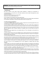
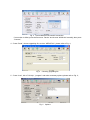
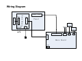
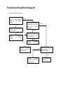
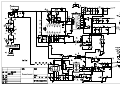
FILE NO.
SERVICE MANUAL
LCD TV
LCD-40XR11F
PRODUCT CODE No.
1 682 350 98: PAL-B/G (Australia)
NTSC(AV)
INPUT
REFERENCE No.:SM0915190
CONTENTS
Safety precautions………………………………………………………………………..… 3
Alignment instructions …………………………….…….………………………………… 5
Software upgrade instructions .................................................................................. 12
Working principle analysis……………………………….………….…………............... 15
Block diagram…………………………………..………………………………….…………17
IC block diagram………………………………………………………………………..……18
Wiring diagram ……………………………………………………………………………. 21
Troubleshooting flow chart ………………………………………………………………..……
22
Schematic diagram………………………………………………………………………… 25
APPENDIX-A: Assembly list
APPENDIX-B: Exploded View
Assembling the Stand
WALL MOUNTING INSTRUCTIONS
Attention: This service manual is only for service personnel to take reference with. Before
servicing please read the following points carefully.
Safety precautions
1. Instructions
Be sure to switch off the power supply before replacing or welding any components or
inserting/plugging in connection wire. Anti static measures must be taken (throughout the entire
production process!):
a) Do not touch here and there by hand at will;
b) Be sure to use anti static electric iron;
c) It’s necessary for the welder to wear anti static gloves.
Please refer to the part list before replacing components that have special safety requirements.
Do not replace with different components with different specs and type at will.
2. LCD servicing precautions
2.1 Screens are different from one model to another and therefore not interchangeable. Be sure to
use the screen of the original model for replacement.
2.2 The operation voltage of LCD screen is 700-825V. Be sure to take proper measures in
protecting yourself and the machine when testing the system in the course of normal operation or
right after the power is switched off. Please do not touch the circuit or the metal part of the module
that is in operation mode. Relevant operation is possible only one minute after the power is
switched off.
2.3 Do not use any adapter that is not identical with the TV set. Otherwise it will cause fire or
damage to the set.
2.4 Never operate the set or do any installation work in bad environment such as wet bathroom,
laundry, kitchen, or nearby fire source, heating equipment and devices or exposure to sunlight etc.
Otherwise bad effect will result.
2.5 If any foreign substance such as water, liquid, metal slices or other matters happens to fall into
the module, be sure to cut the power off immediately and do not move anything on the module lest
it should cause fire or electric shock due to contact with the high voltage or short circuit.
2.6 Should there be smoke, abnormal smell or sound from the module, please shut the power off
at once. Likewise, if the screen is not working after the power is on or in the course of operation,
the power must be cut off immediately and no more operation is allowed under the same
condition.
2.7 Do not pull out or plug in the connection wire when the module is in operation or just after the
power is off because in this case relatively high voltage still remains in the capacitor of the driving
circuit. Please wait at least one minute before the pulling out or plugging in the connection wire.
2.8 When operating or installing LCD please don’t subject the LCD components to bending,
twisting or extrusion, collision lest mishap should result.
2.9 As most of the circuitry in LCD TV set is composed of CMOS integrated circuits, it’s necessary
to pay attention to anti statics. Before servicing LCD TV make sure to take anti static measure and
ensure full grounding for all the parts that have to be grounded.
2.10 There are lots of connection wires between parts behind the LCD screen. When servicing or
moving the set please take care not to touch or scratch them. Once they are damaged the screen
would be unable to work and no way to get it repaired.
If the connection wires, connections or components fixed by the thermotropic glue need to
disengage when service, please soak the thermotropic glue into the alcohol and then pull them
out in case of dagmage.
2.11 Special care must be taken in transporting or handling it. Exquisite shock vibration may lead
to breakage of screen glass or damage to driving circuit. Therefore it must be packed in a strong
case before the transportation or handling.
2.12 For the storage make sure to put it in a place where the environment can be controlled so as
to prevent the temperature and humidity from exceeding the limits as specified in the manual. For
prolonged storage, it is necessary to house it in an anti-moisture bag and put them altogether in
one place. The ambient conditions are tabulated as follows:
Temperature
Humidity
Operation range
+5 ~ +35 oC
Storage range
-20 ~ +60 oC
Operation range
20% ~ 80%
Storage range
10% ~ 90%
2.13 Display of a fixed picture for a long time may cause a permanent after-image on the screen,
as commonly called “ghost shadow”. The degree of the after-image varies with the maker of LCD
screen. This phenomenon doesn’t represent failure. This “ghost shadow” may remain in the
picture for a period of time (several minutes). But when operating it please avoid displaying still
picture in high brightness for a long time.
3. Installation precautions
3.1 The front panel of LCD screen is made of glass. When installing it please make sure to put it in
place.
3.2 For service or installation it’s necessary to use specified screw lest it should damage the
screen.
3.3 Be sure to take anti dust measures. Any foreign substance that happens to fall down between
the screen and the glass will affect the receiving and viewing effect
3.4 When dismantling or mounting the protective partition plate that is used for anti vibration and
insulation please take care to keep it in intactness so as to avoid hidden trouble.
3.5 Be sure to protect the cabinet from damage or scratch during service, dismantling or
mounting.
Adjustment Instruction
1
Safety Instructions
1.1 Power supply must be cut off when replacing or welding any component or inserting / pulling out
connective lines;
1.2 Anti-electrostatic measures must be carried out during the whole producing processes!
a) Do not touch IC by hands at will;
b) Use anti-electrostatic iron;
c) Welder must wear anti-electrostatic glove;
1.3 Replacing any component with special safety requirement must refer to component list without
changing its specification and model at will.
2
Adjustment Equipments
Multimeter or oscilloscope
VG-849
CA-210
USB storage device
DVD ( HDMI 1.4 supported ) or equipments with the same functions
3
Adjustment Processes
3.1 Power voltage checking
According to the wiring diagram specified by “Product Specification”, connect power board
assembly, data processing assembly, IR/Key board assembly, backlight board assembly correctly,
to power on the TV set.
supply with power, press button
Make sure the voltages of socket X601 each pin on the main board are correct.Voltage value
and range are listed as Table 1:
Table 1
Voltage of X601 each pin
X601
Pin1,2
3,4
Voltage
24V±5%
0
Function
AMP_PWR
GND
5,6
12
V±5%
+5V
STB
7,8
9
0
≤5.2V
GND
PWR_SW
10
11
5
5
V±5%
V±5%
Main
+5V
5V
STB
12
13
≤5.2 V
≤5.2 V
BL_PWM
BL_ON
3.2 Adjustment flow as Fig. 1:
Check if EDID、HDCP KEY、FLASH has been written?
General assembly and combined adjustment
White balance adjustment
Input central signal, check TV function (omitted
channel, analog parameters control, etc. ), check
earphone, speakers output.
Check accessory and packing
Check AV input, output and relevant functions.
Default settings before ex-factory
Input Component signal, check YPbPr functions.
Input D-SUB signal, check display and all functions
Check other functions (Radio、
(such as analog parameter), H/V center, etc..
LCN、HDMI ARC/CEC、OAD, etc.)
Input HDMI signal, check display and all functions
(such as analog parameter), H/V center, etc..
Check USB multimedia port and
Fig. 1 Adjustment flow chart
4
Adjustment Instruction
4.1 The unit adjustment
4.1.1
According to the wiring diagram specified by “Product Specification”, connect
power/backlight board assembly, data processing assembly, IR/Key board assembly correctly, supply
with power, turn on the TV set. Check display.
4.1.2
Factory menu instruction
a) Press key “INPUT”, then press digital keys “2、5、8、0” in turn to enter into primary factory
menu;
b)
c)
d)
e)
f)
g)
h)
Press keys “▲” and “▼” to move cursor to each page of primary factory menu, then press
key “OK” to enter into submenu page;
Press keys “▲” and “▼” to move cursor upward or downward within any one page;
Press keys “◄” and “►” to do adjustment when move cursor to one item;
Press key “MENU” to exit submenu page to the superior factory menu;
Press key “EXIT” to exit factory menu in any case;
Press key “OK” to enter the inferior factory submenu;
Factory menu item: Aging Mode to be used for aging the TV set; red, green blue and
white full screen picture displays in turn; default setting is OFF;
i)
Factory menu item: ADC ADJUST
Component;
to be used for ADC calibration for VGA and
j)
Factory menu item: Fac. Channel Preset to be used for factory channel presetting; central
signal digital frequency value for Australia program is set as CH28(529.5 MHz) and
CH33(564.5 MHz); original digital program presetting could not change if central signal
setting has any modification, so please search for digital program manually by perform item
DTV of menu Channel;
k) Factory menu item: Color Temp. to be used for white balance adjustment;
l) Factory menu item: Store Setting Init.
m) Factory menu item: USB SW Update to be used for software updating from USB port;
when U disk containing updating software is inserted into USB port, choose the item to
perform updating process;
n)
Factory menu item: Other Settings include settings of EEPROM Init, MEMC Update,
Power mode, MST DEBUG, ISP MODE, Backlight, SSC, NONLINEAR, Video Quality, Audio
Quality, Light Sensor, Overscan, etc.; no need any adjustment normally.
o)
Factory menu item: Shipment to be used for initializing user data; Success flag will display
after initialization, then press KEY POWER only to power off the TV set.
p)
Please perform EEPROM Init before adjustment for the first time if software has been
upgraded or data have been kept in EEPROM.
4.1.3 ADC calibration for D-SUB channel
a) Switch to D-SUB channel;
b) Press key “INPUT”, then press digital keys “2、5、8、0” in turn to enter into primary factory
menu;
c) Move cursor to item “ADC ADJUST” and press key “OK” to enter into the inferior submenu;
d) Input D-SUB signal (VG-849 Timing:856 (1024×768/60 Hz), Pattern:914 Chess Pattern);
move cursor to item “MODE”, press keys “▲” and “▼” to choose item “RGB”, then move
cursor to item “AUTO ADC” and press key “OK” to perform auto adjustment until prompt
“success” displays;
4.1.4 ADC calibration for Component channel
a) Switch to Component channel;
b) Press key “INPUT”, then press digital keys “2、5、8、0” in turn to enter into primary factory
menu;
c) Move cursor to item “ADC ADJUST” and press key “OK” to enter into the inferior submenu;
d) Input Component signal (VG-849 Timing:972(1080i), Pattern:918 100% color bar); move
cursor to item “MODE”, press keys “▲” and “▼” to choose item “YPbPr”, then move cursor to
item “AUTO ADC” and press key “OK” to perform auto adjustment until prompt “success”
displays;
4.2 White balance adjustment
Unless specified by customer, default settings of COOL color temperature is 12000K and
chromatic coordinates is (272、278); referenced settings of Normal color temperature is 9300K and
chromatic coordinates is (285、293); referenced settings of Warm color temperature is 6500K and
chromatic coordinates is (313、329);
Default setting is Normal.
4.3 Adjustment procedures
The TV set should be working above 30 minutes to be in a stabler state before adjustment. Use
CA-210 BBY channel to adjust white balance;
a) Switch to HDMI channel;
b) Press key “INPUT”, then press digital keys “2、5、8、0” in turn to enter into primary factory
menu;
c)
d)
e)
f)
g)
h)
i)
j)
k)
l)
Move cursor to item “W/B ADJUST” and press key “OK” to enter into the inferior submenu;
Input HDMI signal (VG-849 Timing:856(1024×768/60 Hz),Pattern:921 16 step Gray);
move cursor to item “MODE”, press keys “▲” and “▼” to choose item “HDMI”, then move
cursor to item “TEMPERTURE” and press keys “▲” and “▼” to choose “COOL”;
Fix “G GAIN”, adjust “R GAIN, B GAIN” to set 14th chromatic coordinates as (272、278);
Fix “G OFFSET”, adjust “R OFFSET、B OFFSET” to set 4th chromatic coordinates as
(272、278);
To make sure chromatic coordinates of bright scale are (X=272±10,Y=278±10) and
chromatic coordinates of dark scale are (X=272±10,Y=278±10) during adjusting;
Move cursor to item “COPY ALL” to copy white balance data to other channels except DTV
channel;
Check if chromatic coordinates of NORMAL and WARM meet the requirements (permitted
error of NORMAL bright scale: x±10,y±10, permitted error of NORMAL dark scale: x±10,
y±10; permitted error of WARM bright scale and dark scale: x±10,y±10); if not, adjust
“R_GAIN /B_GAIN/R_OFF/B_OFF” to be up to the requirements and then save the data;
Perform “Copy All” for Normal/Warm adjustments except DTV channel;
Check if chromatic coordinates of other channels meet the requirements, if not, do
adjustment for nonstandard channel alone with the same procedures from b) to j) as HDMI
channel’s and then save the data;
Switch to HDMI channel, change to 16-grey-scale program from central signal source,
adjust white balance with the same procedures from e) to g) as HDMI channel’s; but pay
attention not to perform “COPY ALL”!
m) Inspect all channels after completing adjustment to check if display is normal;
n) Refer to the following rule for adjustment:
B Gain/Offset: adjust B Gain/Offset downward, coordinates of X and Y will increase, adjust B
Gain/Offset upward, coordinates of X and Y will decrease;
R Gain/Offset: adjust R Gain/Offset will affect X value, but affect Lv value slightly, adjust R
Gain/Offset upward, coordinates of X will increase, adjust R Gain/Offset
downward, coordinates of X will decrease;
G Gain/Offset: adjust G Gain/Offset will affect Y value, and affect Lv value greatly, adjust G
Gain/Offset upward, coordinates of Y will increase, adjust G Gain/Offset
downward, coordinates of Y will decrease;
Note: Sanyo customer requires that default color temperature is Normal, adjust white
balance of color temperature Normal and Cool in Dynamic picture mode; for other
customers, please adjust white balance of color temperature Cool in Dynamic picture mode.
5
Function check
5.1 TV functions
Input central signal to RF port, enter into menu Channel first, then search for programs
automatically and check if there is any omitted program; check the speakers output and the picture
display;
5.2 AV port
Input AV signal with formats listed as Table 1 separately, check picture, sound and other
functions;
Table 1 AV video signal formats
No.
Lines per
H.- Freq.(kHz)
frame
Note
V.- Freq.(Hz)
1
525
15.734/15.75
59.94/60
NTSC, NTSC4.43,PAL60,PAL-M
2
625
15.625
50
PAL, PAL-N, SECAM
5.3 Component port
Input Component signal from VG-849 with formats listed as Table 2 separately, check picture and
sound in the case of power-on, switching channel, changing mode, etc.;
Table 2 Component signal formats
No.
Definition
H.- Freq.
V.- Freq.
Dot pulse Freq.
(kHz)
(Hz)
(MHz)
Note
1
720×480
15.734/15.75
59.94/60
13.5/13.514
480i (NTSC)
2
720×576
15.625
50
13.5
576i (PAL)
3
720×480
31.469/31.5
59.94/60
27/27.027
480p (NTSC PROG)
4
720×576
31.25
50
27
576p (PAL PROG)
5
1280×720
37.5
50
74.25
720p (50p)
6
1280×720
44.955/45
59.94/60
74.176/74.25
720p (59.94p/60p)
7
1920×1080
28.125
50
74.25
1080i (50i)
8
1920×1080
33.75
59.94/60
74.176/74.25
1080i (59.94p/60p)
9
1920×1080
26.973
23.976
74.176
1080p (23.97p)
10
1920×1080
27
24
74.25
1080p (24p)
11
1920×1080
28.125
25
74.25
1080p (25p)
12
1920×1080
33.716
29.97
74.176
1080p (29.97p)
13
1920×1080
33.75
30
74.25
1080p (30p)
14
1920×1080
56.25
50
148.5
1080p (50p)
15
1920×1080
67.432/67.5
59.94/60
148.35/148.5
1080p (59.94p/60p)
5.4 D-SUB port
Input D-SUB signal from VG-849 with formats listed as Table 3 separately, check picture and
sound; if H./V. of picture displays abnormally, enter into main menu Picture->Screen->Auto Adjust to
perform auto calibration.
Table 3 D-SUB signal formats
No.
Definition
H.- Freq.
V.- Freq.
Dot pulse Freq.
(kHz)
(Hz)
(MHz)
Note
1
640×480
31.469
59.94
25.175
IBM
2
720×400
31.469
70.086
28.322
IBM
3
640×480
37.861
72.809
31.5
VESA
4
640×480
37.5
75
31.5
VESA
5
800×600
35.156
56.25
36
VESA
6
800×600
37.879
60.317
40
VESA
7
800×600
48.077
72.188
50
VESA
8
800×600
46.875
75
49.5
VESA
9
1024×768
48.363
60.004
65
VESA
10
1024×768
56.476
70.069
75
VESA
11
1024×768
60.023
75.029
78.75
VESA
12
1152×864
67.5
75
108
VESA
13
1280×960
60
60
108
VESA
14
1280×1024
63.98
60.02
108
VESA
15
1280×1024
80
75
135
SXGA
16
1360×768
47.7
60
85.5
WXGA
17
1440×900
55.9
60
106.5
18
1680×1050
65.3
60
146.25
19
1920×1080
67.5
60
148.5
WXGA+
(
Panel
National only)
WSXGA+ ( Panel
National only)
5.5 HDMI port
HDMI port supports all signal formats supported by Component port (Table 2) and D-SUB port
(Table 3), furthermore, it can also support signal with formats listed as Table 4 and Table 5 (video and
audio combination). Check picture and sound in the case of power-on, switching channel, changing
mode, etc.;
Table 4
Digital HDMI signal formats
No
.
Definition
H.- Freq.
V.- Freq.
(kHz)
(Hz)
Dot pulse
Freq.
Note
(MHz)
1
720(1440)×480
15.734/15.75
59.94/60
27/27.027
2
720(1440)×576
15.625
50
27
720(1440)×[email protected]/60 Hz,
4:3/16:9
720(1440)×576i@50 Hz,4:3/16:9
Table 5
No.
Item
Video & audio signal formats of digital HDMI
Unit
Parameter
Note
Deep color:RGB 4:4:4(24 bit/pixel,30 bit/pixel,36 bit/pixel)、
1
YUV 4:4:4 (24 bit/pixel,30 bit/pixel,36 bit/pixel)、
Video
For "1080p,deep color", only support "30 bit/pixel"
YUV 4:2:2(16 bit)、YUV 4:2:2(20 bit)、YUV 4:2:2(24 bit)
2
3
Audio sample
freqence
Audio
width
data
kHz
32、44.1、48
Bit
16、20、24
5.6 USB port
5.6.1 PVR function
Insert a formatted U disk in which recorded programs have been saved; press key “Record
List” to choose and play one program, check picture, sound and other functions;
5.6.2 Media playing function
Insert a U disk kept files of picture, sound and video, check picture, sound and other
functions;
Supported media formats as below:
Photo:JPEG,BMP,PNG
Video:H.264 ,MPEG-1,MPEG-2,VC-1,FLV
Audio:WMA,MP3,M4A (AAC)
5.7 Music port (depending on different models whether contain the port or not)
Input audio signal to side music port (analog audio input) from audio output equipment, check
audio output.
5.8 Other functions check
a) Check timing on/off, sleeping time off, picture/sound mode, OSD, stereo, digital audio port,
etc,;
b) Check pure digital audio programs (RADIO) ;
c) Check logical channel number (LCN);
d) Check HDMI ARC;
e) Check HDMI CEC;
f) Check OAD for special customer;
6
User Menu Setting before shipment
Enter into Factory Menu and choose “Shipment” to perform presetting before shipment;
Main procedures are described as follow:
a) Clear out all programs;
b) Clear out information of VCHIP,parent control, etc.;
c) Default user analog parameter setting;
d) Recover default password;
e) Set Menu Language as English;
f) Set Power mode as Off。
Software Upgrading Instruction
Software Upgrading Instruction as Table 6
Table 6
Location
Part No.
Software Upgrading Instruction
Software
SMT before
function
upgrading
Part model
Upgrading method
Upgrade with ALL100, etc.,
N103
5272532006
EN25Q32A-100HIP
FLASH
Yes
need write protection, refer to
Note1;
N105
5272404005
CAT24C04WI-GT3
HDCP KEY
Yes
NB03
5272402003
CAT24C02WI
VGA EDID
Yes
Upgrade with ALL100, etc.
Note 1
Write protection setting method: enter into ALL-100 upgrading interface “AUTO”, tick off
“Config”, press “config Setting”, set option “Protect” as “All Protect” and “SRWD” as “Enable”,
then press “OK” to complete write protection setting;
Please make sure option “Config” is ticked off during software upgrading and reset write
protection after ALL-100 upgrading software is opened each time;
Note 2 Upgrading method with ISP upgrading instrument:
1) Main board upgrading: connect 4-core line of ISP to Debug port (X603) on main board;
The Unit upgrading: connect both VGA ports of ISP and main board, enter into factory menu and
set “ISP Mode” as “ON”;
2) Use Mstar upgrading instrument (V4.4.2.0 or higher version), enter into menu “Device”, tick off
“WP Pin pull to high during ISP” to make sure Flash hardware write protection is removed and
erasing process is normal; please refer to Fig.2;
Fig. 2 Write protection setting
3) Press menu “Connect”, dialog box “Device Type is MX25L64” (device type depending on parts
used on board actually) will display to show successful connection; please refer to Fig. 3;
Fig. 3 Device MX25L64 successful connection
If connection is failed, press the first menu “Device” and choose “MX25L64” manually, then press
“Connect”;
4) Press “Read”, choose upgrading file, such as “MERGE.bin”; please refer to Fig. 4;
Fig. 4
Choosing upgrading file
5) Press “Auto”, tick off “All chip”, “program” and other necessary options; please refer to Fig. 5;
Fig. 5
Options
6) Press “Run” shown as Fig. 4 to perform upgrading in two steps, “Erase” and “Program”;
Normal upgrading process:
The first step “Erasing…, Flash Status: 03” will last for some time, or erasing is failed if the step
passes over immediately; please confirm procedure 2) to perform upgrading again;
The second step is “Programming…,Flash Status:00”;
Then prompt “Pass” displays;
7) Prompt “Pass” will display by button “Run” when upgrading succeeds; please refer to Fig. 6;
Fig. 6 Prompt “Pass” displayed by “Run” when upgrading succeeds
8) Need not exit ISP upgrading interface if there are other TV sets to be upgraded , only procedures
3) and 6) need repeat;
Note 3
Upgrading with USB:
1) Make sure U disk is formatted as FAT32;
2) Copy software file named as “Merge. bin” to U disk;
3) Turn on the TV set, then insert U disk in USB port of the unit;
a)
First press key “INPUT”, then press keys “2、5、8、0” in turn to enter into primary factory
menu;
b)
Choose “USB SW Update” to begin upgrading;
4) Upgrading processes:
A、Read data from U disk while data indicator light of U disk is twinkling at the same time;
B、Upgrading flash, then the unit will be in “standby” mode;
5) Cut off the power supply and then restart the TV set, enter into factory menu to verify version and
time parameter, then perform “EEPROM Init” to complete the whole upgrading processes.
Note: The USB upgrading method can not be sure to be suitable for all kinds of U disk, so try another U
disk if necessary.
Working Principle of the Unit
1、 ATV
PAL signal flow
Receive RF PAL analog signal and sent it to XC5200C (D/A silicon Tuner controlled by main chip
MSD309PX through I2C bus) to be demodulated, then differential IF signal is send out to main chip
MSD309PX analog demodulation to be demodulated to get analog CVBS video signal and SIF sound
signal.
CVBS video signal is processed by back-end video decoder, anti-interlacing part, video processor
and zoom controller, then LVDS signal is outputted to drive display panel.
SIF sound signal is processed by back-end demodulator to get analog sound signal, then processed
by pre-amplifier, acoustic effect processor and volume controller to get two parts of signals: the analog
part of signal is sent to earphone amplifier MAX9820 to be amplified and then outputted to earphone jack;
the digital part of signal I2S is sent to digital audio power amplifier TAS5711 to be processed by D/A
converter and power amplifier, then outputted to drive speakers.
2、 DVB-T signal flow
Receive RF DVB-T digital signal and sent it to XC5200C (D/A silicon Tuner controlled by main chip
MSD309PX through I2C bus) to be processed by down-frequency-conversion, then differential IF signal is
send out to main chip MSD309PX digital demodulation to be demodulated, then standard parallel
transmission flow is outputted to back-end demultiplexer and decoder to be processed.
Video channel: demultiplexing digital video signal is processed by MSD309PX decoder and video
processor, then LVDS signal is outputted to drive display panel;
Audio channel: demultiplexing digital audio signal is processed by MSD309PX decoder and audio
processor, then double-sound-track analog audio signal (stereo) is outputted to MSD309PX to be
processed by preamplifier, acoustic effect processor and volume controller to get two parts of signals: the
analog part of signal is sent to earphone amplifier MAX9820 to be amplified and then outputted to
earphone jack; the digital part of signal I2S is sent to digital audio power amplifier TAS5711 to be
processed by D/A converter and power amplifier, then outputted to drive speakers.
3、 AV input signal flow
AV video signal is inputted to main chip MSD309PX to be processed by video decoder,
anti-interlacing part, video processor and zoom controller, then LVDS signal is outputted to drive display
panel;
AV audio signal is processed by voltage divider, resistance matcher and AC coupler, then sent to
main chip MSD309PX to be processed by acoustic effect processor and volume controller to get two parts
of signals: the analog part of signal is sent to earphone power amplifier MAX9820 to be amplified and
then outputted to earphone jack; the digital part of signal I2S is sent to digital audio power amplifier
TAS5711 to be processed by D/A converter and power amplifier, then outputted to drive speakers.
4、 D-SUB/YPbPr input signal flow
D-SUB、YPbPr video signal is inputted to main chip MSD309PX to be processed by A/D convertor,
video decoder, anti-interlacing part, video processor and zoom controller, then LVDS signal is outputted to
drive display panel;
D-SUB、YPbP audio signal is processed by voltage divider, resistance matcher and AC coupler, then
sent to main chip MSD309PX to be processed by acoustic effect processor and volume controller to get
two parts of signals: the analog part of signal is sent to earphone power amplifier MAX9820 to be
amplified and then outputted to earphone jack; the digital part of signal I2S is sent to digital audio power
amplifier TAS5711 to be processed by D/A convertor and power amplifier, then outputted to drive
speakers.
5、 HDMI input signal flow
HDMI video signal is inputted to main chip MSD309PX to be processed by video decoder, video
processor and zoom controller, then LVDS signal is outputted to drive display panel;
HDMI audio signal is sent to main chip MSD309PX to be processed by audio decoder, pre-amplifier,
acoustic effect processor and volume controller to get two parts of signals: the analog part of signal is sent
to earphone power amplifier MAX9820 to be amplified and then outputted to earphone jack; the digital
part of signal I2S is sent to digital audio power amplifier TAS5711 to be processed by D/A convertor and
power amplifier, then outputted to drive speakers.
Block Diagram
RF
XC5200C
Silicon
Tuner
VIF
LVDS
SIF
HDMI1 w/ARC
I2S
HDMI2
TAS5711
Audio
Amplfier
HDMI3
VGA
MSD309PX-LF
YPbPr
DDR2
512Mbit X 2PCS
Video In
YPbPr Audio In
Flash
AV Audio In
VGA Audio In
SPDIF IN
IR
USB
RS-232
MAX232
POWER
SUPPLY
KEY
IC Block Diagram
1、
TUNER IC XC5200C
The Single-Chip Multi-Standard Tuner XC5200C supports all analog TV
formats transmitted worldwide in the 42-1000 MHz band on either cable or
terrestrial broadcast channels. It implements on-chip tuning, and channel
filtering without external (SAW) filters and has no manually tunable parts.
The broadband tuner converts the selected channel into an Intermediate
Frequency (IF), which is then sampled by an internal high-resolution
analog-to-digital converter (A/D) for further processing.
The IF signals are filtered using a standard-dependent high-rejection
channel filter and converted to a user programmable output frequency. At the
output of the D/A converter, the TV signal is low-pass filtered using a
high-performance smoothing filter and input to a variable gain amplifier. The IF
output amplifier gain can be controlled via an external analog signal on Vagc.
The XC5200C architecture is summarized in Figure 1. XC5200C Block
Diagram.
2、
AMP IC
TAS5711
The TAS5711 is a 20-W, efficient, digital audio power amplifier for driving
stereo bridge-tied
speakers. One serial data input allows processing of up to two discrete audio
channels and seamless integration to most digital audio processors and MPEG
decoders. The device accepts a wide range of input data and data rates. A fully
programmable data path routes these channels to the internal speaker drivers.
The TAS5711 is an I2S slave-only device receiving all clocks from external
sources. The TAS5711
operates with a PWM carrier between 384-kHz switching rate and 352-KHz
switching rate depending on the input sample rate. Over sampling combined
with a fourth-order noise shaper provides a flat noise floor and excellent
dynamic range from 20 Hz to 20 kHz.
3、
AUDIO IC MAX9820
The MAX9820 Windows Vista®-compliant stereo headphone amplifier is
designed for portable
Equipment where board space is at a premium. It features Maxim’s
DirectDrive® architecture to produce a ground-referenced output from a single
supply, eliminating the large output-coupling capacitors required by
conventional single-supply headphone amplifiers.
The MAX9820 features an undervoltage lockout that prevents over
discharging of the battery
During brownout conditions, click-and-pop suppression that eliminates audible
transients on startup, a low-power shutdown mode, and thermal-overload and
short-circuit protection. Additionally, the MAX9820 suppresses RF radiation
received by input and supply traces acting as
antennas and prevents the amplifier from demodulating the coupled noise.
Wiring Diagram
Inverter
X502
Power Board
X503
Panel TCON
X508
Panel
IR
Board
X501
Key
Board
LVDS
Power
X601
X603
Debug
X401
AMP
XV01
Main Board
IR
X604
Key
X610
Troubleshooting Block Diagram
1.Panel doesn’t light up.
Supply with power,
check if red indicator
lights up in STANDBY
state?
Yes
Press key POWER
on remote control or
the
unit,
check
indicator.
No
Check if 5V is supplied
to X601-PIN11 ?
Blue
No
Check
circuits
board.
Red
Check if level of
X601-PIN13 on main
board is high?
STANDBY
on
power
Yes
No
Check
board.
backlight
Check
power
control circuits on
main board.
No
Check if level of
X601-PIN9 on main
board is high?
Yes
Check
power
control circuits on
main board.
Check power
board.
2.No picture, but backlight is normal:
Can control the TV set
by keys on remote
control or the unit?
Yes
Press key MENU,
can OSD display
normally?
Yes
No
No
Yes
No
有
Enter into factory menu to initialize
EEPROM, then cut off main power
and then turn on the TV set again,
check if there is picture?
Yes
Readjust the
main board.
Replace the main
board
Do no
TVchannel
have picture at
all?
No
3.No sound, but picture is normal:
No sound
Check if level of
NV01-PIN19&25
are all high?
No
Yes
Check if there is
signal inputted to
NV01-PIN15&20&21
&22 ?
No
Check
IIS
(signal
input
circuits) on main
board.
No
Check +24V on
power board.
Yes
Check if level of
VV03-b is low?
Yes
No
Replace
VV03
Check Reset &
Mute circuits of
power amplifier.
Check power voltage
of NV01.
Yes
Check IIC signal of
NV01- PIN23&24.
D
E
N101 -A
F7
E8
MA_DQS1
MA_DQSB1
ODT
VSSQ1
VSSQ2
VSSQ3
VSSQ4
VSSQ5
VSSQ6
VSSQ7
VSSQ8
VSSQ9
VSSQ10
LDQS
LDQS
B7
A8
UDQS
UDQS
A_MVERF
J2
A2
E2
L1
R3
R7
R8
MA_BA2
3
VREF
MA_A13
NC#A2
NC#E2
BA2
NC#R3
NC#R7
NC#R8
MIUA_DQS1
MIUA_DQSB1 R126
A7
B2
B8
D2
D8
E7
F2
F8
H2
H8
MIUA_DQ11
MIUA_DQ12
MIUA_DQ9
MIUA_DQ14
R105
10K
A3
E3
J3
N1
P9
VSS1
VSS2
VSS3
VSS4
VSS5
MIUA_DQ6
MIUA_DQ1
MIUA_DQ3
MIUA_DQ4
+1.8V-DDR2
MIUA_DQ15
MIUA_DQ8
MIUA_DQ10
MIUA_DQ13
A_MVERF
R106
10K
C105
100n
MIUA_DQ7
MIUA_DQ0
MIUA_DQ2
MIUA_DQ5
GND-D
GND-D
R127
R128
R129
R130
MA_DQS0
22 MA_DQSB0
MIUA_DQS0
MIUA_DQSB0
MIUA_DQS1
MIUA_DQSB1
A16
C16
A15
B15
MIUA_DQM0
MIUA_DQM1
B16
C17
MA_DQS1
22 MA_DQSB1
MIUA_MCLK C12
MIUA_MCLKZ B11
MIUA_MCKE C21
MA_DQ11
GND-D MA_DQ12
22 MA_DQ9
MA_DQ14
MIUA_WEZ
MIUA_RASZ
MIUA_CASZ
MIUA_BA0
MIUA_BA1
MIUA_BA2
MIUA_ODT
MA_DQ6
MA_DQ1
22 MA_DQ3
MA_DQ4
MA_DQ15
MA_DQ8
22 MA_DQ10
MA_DQ13
B20
B10
A10
A21
B21
C22
C11
PAD_IO[59](B_MCLK)
PAD_IO[57](B_MCLKZ)
PAD_IO[84](B_CKE)
PAD_IO[83](B_WEZ)
PAD_IO[56](B_RASZ)
PAD_IO[54](B_CASZ)
PAD_IO[86](B_BA0)
PAD_IO[85](B_BA1)
PAD_IO[87](B_BA2)
PAD_IO[58](B_ODT)
PAD_IO[36](A_WEZ)
PAD_IO[9](A_RASZ)
PAD_IO[7](A_CASZ)
PAD_IO[39](A_BA0)
PAD_IO[38](A_BA1)
PAD_IO[40](A_BA2)
PAD_IO[11](A_ODT)
L24
L23
K24
K25
MIUB_DQS0
MIUB_DQSB0
MIUB_DQS1
MIUB_DQSB1
MIUB_DQS0
MIUB_DQSB0 R157
M23
M24
MIUB_DQM0
MIUB_DQM1
MIUB_DQS1
MIUB_DQSB1 R158
G23
F25
T23
MIUB_MCLK
MIUB_MCLKZ
MIUB_MCKE
MIUB_DQ11
MIUB_DQ12 GND-D
MIUB_DQ9 R159
MIUB_DQ14
R25
F23
E24
T24
T25
U23
F24
MIUB_WEZ
MIUB_RASZ
MIUB_CASZ
MIUB_BA0
MIUB_BA1
MIUB_BA2
MIUB_ODT
MIUB_DQ6
MIUB_DQ1
MIUB_DQ3
MIUB_DQ4
+1.8V-DDR2
R143
10K
D22
R141
10K
C109
100n
KEY
+5V-HDMI1_DET
002:C3
4
SPI-CK
SPI-DI
SPI-CSSPI-DO
+3.3V-S
+3.3V-S
N103
EN25Q64-104HIP
SPI
003:D1
LED
C4
A4
A2
B3
A3
B2
1
8
CS
VCC
R102
10K
2
7
R101
10K
C101
100n
NC/DQ3
DO/DQ1
CLK
WP/DQ2
3
6
5
R103
10K
4
DI/DQ0
R118
VSS
22
+3.3V-S
C103
100n
R175
10K
R176
10K
PAD_GPIO_PM6(BOOT_FLASH_CS)
PAD_SPI_CZ(BACKUP_FLASH_CS)
PAD_SPI_CK
PAD_SPI_DI
PAD_SPI_DO
PAD_GPIO_PM8(FLASH_WP)
UART/I2CS
P6
N6
003:F1;002:A2;002:G1 UART-RX
003:F1;002:A2;002:G1 UART-TX
GND-D
PAD_SAR0
PAD_SAR1
PAD_SAR2(POWER_DET)
PAD_SAR3
DDCA_CK
DDCA_DA
I2CM
001:A6;003:D1;003:E3;004:B5
AA23
AA24
SCL
001:A6;003:D1;003:E2;004:B5
SDA
PAD_DDCR_CK
PAD_DDCR_DA
IR
G5
003:D1 IR
PAD_IRIN
R113
1M
C106
30p
5
G101
24MHz
+3.3V-S
Vcc
C102
100n
C107
R104 GND-D 30p
10K
GND
N105
CAT24C04WI
R137
10K
1
Vcc
2 NC1
3 A1 HDCP WP
SCL
4 A2
Vss
SDA
8
7
6
5
RESET
R146 33
R147 33
R145
0
USB
USB-D+
USB-D-
C2
B1
AD11
AE11
F11
E11
GND-D
R177
10K
8
A0
Vcc
A1
WP
2
R178 33
R179 33
R180 33
7
3
A2
DATA
6
SCL
4
5
SDA
100n
C133
GND
GND-D
Option
GND-D
R133
0
AC20
AD21
AE20
AD20
AE19
AC19
AC18
AD19
AC17
AD18
AE17
AD17
R134
0
R132
R135
R136
0
0
0
0
RXO0+
RXO0RXO1+
RXO1RXO2+
RXO2RXOC+
RXOCRXO3+
RXO3RXO4+
RXO4-
004:D5;004:E6
004:C5;004:E6
004:D5;004:E6
004:C5;004:E6
004:D5;004:E5
004:C5;004:E5
004:D5;004:E5
004:C5;004:E5
004:D5;004:E5
004:C5;004:E5
004:D5
004:C5
RXE0+
RXE0RXE1+
RXE1RXE2+
RXE2RXEC+
RXECRXE3+
RXE3RXE4+
RXE4-
004:D5
004:C5
004:D5
004:C5
004:D5
004:C5
004:D5
004:C5
004:D5
004:C5
004:D6
004:C6
GPIO_TCON
PAD_TCON0
PAD_TCON1(SC1_RE1)
PAD_TCON2(FE_ANT5V_MONITOR)
PAD_TCON3(TUNER_RESET)
PAD_TCON4
PAD_TCON5(SC1_MUTE)
PAD_TCON6(PCM_5V_CTL)
PAD_TCON7(SIDE_AV_DET)
PAD_TCON9(COMP_DET)
PAD_TCON10(HP_DET)
PAD_TCON11(HP_MUTE)
PAD_DP_P0
PAD_DM_P0
PAD_DP_P1
PAD_DM_P1
PAD_GND_EFUSE
PAD_TESTPINPP
B7
A8
MB_DQ7
MB_DQ0
22 MB_DQ2
MB_DQ5
MB_A13
R160
R162
ODT
UDQS
UDQS
J2
VREF
A2
E2
L1
R3
R7
R8
MB_BA2
VSSQ1
VSSQ2
VSSQ3
VSSQ4
VSSQ5
VSSQ6
VSSQ7
VSSQ8
VSSQ9
VSSQ10
LDQS
LDQS
NC#A2
NC#E2
BA2
NC#R3
NC#R7
NC#R8
VSS1
VSS2
VSS3
VSS4
VSS5
GND-D
+1.8V-DDR2
J1
J7
A7
B2
B8
D2
D8
E7
F2
F8
H2
H8
GND-D
+1.8V-DDR2
R169
10K
A3
E3
J3
N1
P9
R170
10K
B_MVERF
C113
100n
GND-D
Close to DDR
AA10
T5
AB10
AB7
AA9
V5
AC11
AA8
E2PWP0
001:A6
R183
MUTE_AVOUT
0
002:D5
R185
R6
Y8
Y9
ARC1_CTL 002:D4
HP-DCT- 002:H4
HP-MUTE- 002:F5
N101 -C MSD309PX-LF-V1
N101 -E MSD309PX-LF-V1
HDMI
002:A4
002:A4
002:A4
002:A4
002:A4
002:A4
002:A4
002:A4
002:A4
002:A4
002:A5
002:A3
002:A2
002:A2
002:A2
002:A2
002:A2
002:A3
002:A3
002:A3
002:A3
002:A3
002:A5
002:A5
002:A5
002:A5
002:A5
002:A5
002:A6
002:A5
002:A6
002:A6
002:A6
002:A3;002:A4;002:A6
T4
G2
H3
H2
J3
J2
J1
G3
G1
M4
M5
K6
HDMI2-RX0HDMI2-RX0+
HDMI2-RX1HDMI2-RX1+
HDMI2-RX2HDMI2-RX2+
HDMI2-RXCHDMI2-RXC+
HDMI2-SCL
HDMI2-SDA
HDMI2-HP
D2
E3
E2
F3
F2
F1
D3
D1
J6
L6
J4
HDMI1-RX0HDMI1-RX0+
HDMI1-RX1HDMI1-RX1+
HDMI1-RX2HDMI1-RX2+
HDMI1-RXCHDMI1-RXC+
HDMI1-SCL
HDMI1-SDA
HDMI1-HP
HDMI3-RX0HDMI3-RX0+
HDMI3-RX1HDMI3-RX1+
HDMI3-RX2HDMI3-RX2+
HDMI3-RXCHDMI3-RXC+
HDMI3-SCL
HDMI3-SDA
HDMI3-HP
AC8
AD9
AC9
AD10
AE10
AC10
AE8
AD8
AE7
AD7
AC7
R142
100
HDMI-CEC
PAD_RX0N_B
PAD_RX0P_B
PAD_RX1N_B
PAD_RX1P_B
PAD_RX2N_B
PAD_RX2P_B
PAD_RXCN_B
PAD_RXCP_B
DDCDB_CK
DDCDB_DA
HOTPLUGB
PAD_RX0N_C
PAD_RX0P_C
PAD_RX1N_C
PAD_RX1P_C
PAD_RX2N_C
PAD_RX2P_C
PAD_RXCN_C
PAD_RXCP_C
DDCDC_CK
DDCDC_DA
HOTPLUGC
PAD_LINEIN_L0
PAD_LINEIN_R0
PAD_LINEIN_L1
PAD_LINEIN_R1
PAD_LINEIN_L2
PAD_LINEIN_R2
PAD_LINEIN_L5
PAD_LINEIN_R5
PAD_LINEOUT_L0
PAD_LINEOUT_R0
PAD_LINEOUT_L3
PAD_LINEOUT_R3
PAD_EARPHONE_OUTL
PAD_EARPHONE_OUTR
R4
R5
T6
U6
V6
U5
AD6
AC6
V1
V2
AA6
Y5
AD5
AE5
VGA-LIN
VGA-RIN
YPBPR-LIN
YPBPR-RIN
CVBS1-LIN
CVBS1-RIN
MP3-LIN
MP3-RIN
002:G1
002:G1
002:D1
002:D1
002:D6
002:D6
002:G3
002:G3
CVBS-LOUT
CVBS-ROUT
002:D4
002:D4
HPAMP-LIN
HPAMP-RIN
002:G4
002:F4
AB4
AB5
AC3
I2S
PAD_I2S_OUT_MCK
PAD_I2S_OUT_SD
PAD_I2S_OUT_WS
PAD_I2S_OUT_BCK
PAD_I2S_IN_BCK(USB0_OCD)
PAD_I2S_IN_SD(USB0_CTL)
PAD_I2S_IN_WS
A6
B5
B6
C6
C1
H6
G6
SPDIF
P5
PAD_SPDIF_OUT
002:H1
002:G2
002:H1
002:G2
002:H1
002:G2
002:G2
002:G2
002:G2
VGA-R_INVGA-R_IN
VGA-G_INVGA-G_IN
VGA-B_INVGA-B_IN
VGA-SOG_IN
VGA-HSYNC
VGA-VSYNC
+3.3V
GND-D
SPDIF
2.2u
C112
2.2u
L101
BG1608B121
GND-D
MCLK
SDIN
LRCLK
SCLK
003:E2
003:E2
003:E2
003:E2
M2
M3
L2
L3
K1
K3
K2
N4
N5
R3
P2
P3
N2
N3
M1
N1
W6
Y6
Close to 309
C111
PAD_VRP
PAD_VAG
AVSS_VRM_ADC_DAC
K5
PAD_CEC
+3.3V-S
AUDIO
PAD_RX0N_A
PAD_RX0P_A
PAD_RX1N_A
PAD_RX1P_A
PAD_RX2N_A
PAD_RX2P_A
PAD_RXCN_A
PAD_RXCP_A
DDCDA_CK
DDCDA_DA
PAD_HOTPLUGA
002:D3
002:D2
002:D3
002:D2
002:D3
002:D2
002:D2
YPBPR-PR_INYPBPR-PR_IN
YPBPR-Y_INYPBPR-Y_IN
YPBPR-PB_INYPBPR-PB_IN
YPBPR-SOG_IN
U2
U3
T2
T1
R1
R2
T3
V4
RGB
CVBS
PADA_RIN0M
PADA_RIN0P
PADA_GIN0M
PADA_GIN0P
PADA_BIN0M
PADA_BIN0P
PADA_SOGIN0
PAD_HSYNC0
PAD_VSYNC0
PADA_CVBS0
PADA_CVBS1
PADA_CVBS2
PADA_CVBS3
PADA_CVBS4
PADA_CVBS5
PADA_CVBS_OUT1
PADA_CVBS_OUT2
AC5
W4
W5
AA5
W2
W3
V3
AA4
W1
PADA_RIN1M
PADA_RIN1P
PADA_GIN1M
PADA_GIN1P
PADA_BIN1M
PADA_BIN1P
PADA_SOGIN1
PAD_HSYNC1
PAD_VSYNC1
CVBS1_IN 002:D6
CVBS_OUT
002:D5
R174
68
PADA_VCOM
C130
47n
GND-D
PADA_RIN2M
PADA_RIN2P
PADA_GIN2M
PADA_GIN2P
PADA_BIN2M
PADA_BIN2P
PADA_SOGIN2
PADA_HSYNC2
002:D3;002:E1
GPIO
PAD_GPIO0(NTP_MUTE)
PAD_GPIO1(AMP_RST)
PAD_GPIO2(INV_CTL)
PAD_GPIO3(PANEL_CTL)
PAD_GPIO4(USB_CTL)
PAD_GPIO5(ERROR_OUT)
PAD_GPIO12(AMD_SCL)
PAD_GPIO13(AMP_SDA)
A7
C7
F4
E4
C3
D4
F6
F5
RESET-AMP
STB-AMP
BL_SWPNPWR_SW
USB_CTL
003:E3
003:E3
003:B1
003:F5
003:F5
LVDS_IO1
LVDS_IO2
004:B5
004:B5
TITLE:
GPIO_PM
PAD_GPIO_PM0(5V_HDMI_3)
PAD_GPIO_PM1(5V_HDMI_1)
PAD_GPIO_PM4(POWER_ON_OFF)
PAD_GPIO_PM5(5V_HDMI_2)
PAD_GPIO_PM11(DSUB_DET)
PAD_GPIO_PM12(EDID_WP)
+3.3V
1
R131
PAD_TCON15(SC1_DET)
C104
100n
GND-D
N107
AT24LC32A/SN
PADA_OUTP_CH[12](PAD_G_ODD[3])
PADA_OUTN_CH[12](PAD_G_ODD[2])
PADA_OUTP_CH[13](PAD_G_ODD[1])
PADA_OUTN_CH[13](PAD_G_ODD[0])
PADA_OUTP_CH[14](PAD_B_ODD[7])
PADA_OUTN_CH[14](PAD_B_ODD[6])
PADA_OUTP_CH[15](PAD_B_ODD[5])
PADA_OUTN_CH[15](PAD_B_ODD[4])
PADA_OUTP_CH[16](PAD_B_ODD[3])
PADA_OUTN_CH[16](PAD_B_ODD[2])
PADA_OUTP_CH[17](PAD_B_ODD[1])
PADA_OUTN_CH[17](PAD_B_ODD[0])
AC24
AC25
AD24
AD25
AE24
AC23
AE23
AD23
AE22
AC22
AC21
AD22
E5
Option
R181
33
R144
10K
C110
100n
6
PAD_XTAL_IN
PAD_XTAL_OUT
MB_DQS1
MB_DQSB1
VDDL
VSSDL
Close to 309
PADA_OUTP_CH[6](PAD_R_ODD[7])
PADA_OUTN_CH[6](PAD_R_ODD[6])
PADA_OUTP_CH[7](PAD_R_ODD[5])
PADA_OUTN_CH[7](PAD_R_ODD[4])
PADA_OUTP_CH[8](PAD_R_ODD[3])
PADA_OUTN_CH[8](PAD_R_ODD[2])
PADA_OUTP_CH[9](PAD_R_ODD[1])
PADA_OUTN_CH[9](PAD_R_ODD[0])
PADA_OUTP_CH[10](PAD_G_ODD[7])
PADA_OUTN_CH[10](PAD_G_ODD[6])
PADA_OUTP_CH[11](PAD_G_ODD[5])
PADA_OUTN_CH[11](PAD_G_ODD[4])
PAD_RESET
002:A1
002:A1
+3.3V
R111
0
RESET
N104
APX810-29SAG-7
GND-D
+3.3V
XTAL
AD1
AE2
F7
E8
MIUB_DQ7
MIUB_DQ0
MIUB_DQ2
MIUB_DQ5
HDMI2
003:C1;003:H4
J5
G4
B4
AA7
MB_DQ11
GND-DMB_DQ12
22 MB_DQ9
MB_DQ14
LDM
UDM
K9
MB_DQS0
MB_DQSB0
MIUB_DQ15
MIUB_DQ8
MIUB_DQ10 R161
MIUB_DQ13
HDMI1
SAR
MB_DQS1
22 MB_DQSB1
B_MVERF
HDMI3
BL_PWM
003:B1;004:B5
PAD_PWM0
PAD_PWM1
PAD_PWM2
PAD_PWM3
F3
B3
A1
E1
J9
M9
R1
33K
R182
GND-D
AB25
AB24
E6
D6
VDD1
VDD2
VDD3
VDD4
VDD5
RAS
+1.8V-DDR2
MSD309PX-LF-V1
PWM
10K
10K
MB_DQM0
MB_DQM1
MB_DQS0
22 MB_DQSB0
MB_DQ6
MB_DQ1
22 MB_DQ3
MB_DQ4
MB_DQ15
MB_DQ8
22 MB_DQ10
MB_DQ13
Close to DDR
R107
R108
K7
L7
MB_ODT
GND-D
N101 -D
MB_CASZ
WE
CAS
MVREF
MA_DQ7
MA_DQ0
22 MA_DQ2
MA_DQ5
MB_RASZ
MB_DQM1
MB_DQM0
CS
100n
C131
PAD_IO[12](A_MCLK)
PAD_IO[10](A_MCLKZ)
PAD_IO[37](A_CKE)
CKE
L8
GND-D
K3
MB_WEZ
100n
C128
PAD_IO[73](B_DQM0)
PAD_IO[72](B_DQM1)
22
K2
100n
C126
PAD_IO[26](A_DQM0)
PAD_IO[25](A_DQM1)
22
MB_MCLK
MB_MCLKZ
MB_CKE
100n
C124
PAD_IO[70](B_DQS0)
PAD_IO[71](B_DQS0B)
PAD_IO[68](B_DQS1)
PAD_IO[69](B_DQS1B)
MIUB_DQM1
MIUB_DQM0 R156
MB_A13
GND-D
Close to DDR
100n
C122
PAD_IO[23](A_DQS0)
PAD_IO[24](A_DQS0B)
PAD_IO[21](A_DQS1)
PAD_IO[22](A_DQS1B)
MIUB_MCLK
MIUB_MCLKZ R155
75
C114
47n
+1.8V-DDR2
A9
C1
C3
C7
C9
E9
G1
G3
G7
G9
100n
C132
MA_DQS0
MA_DQSB0
VDDL
VSSDL
MA_DQM1
MA_DQM0
R154
VDDQ1
VDDQ2
VDDQ3
VDDQ4
VDDQ5
VDDQ6
VDDQ7
VDDQ8
VDDQ9
VDDQ10
CK
CK
R172
100
100n
C129
K9
MIUA_DQS0
MIUA_DQSB0 R125
J1
J7
22
MIUB_A13
MB_MCLKZ K8
MB_MCLK J8
MB_MCLK
MB_MCLKZ
R171
100
100n
C127
MA_ODT
LDM
UDM
R124
MIUB_DQ0
MIUB_DQ1
MIUB_DQ2
MIUB_DQ3
MIUB_DQ4
MIUB_DQ5
MIUB_DQ6
MIUB_DQ7
MIUB_DQ8
MIUB_DQ9
MIUB_DQ10
MIUB_DQ11
MIUB_DQ12
MIUB_DQ13
MIUB_DQ14
MIUB_DQ15
MB_DQ15
MB_DQ14
MB_DQ13
MB_DQ12
MB_DQ11
MB_DQ10
MB_DQ9
MB_DQ8
MB_DQ7
MB_DQ6
MB_DQ5
MB_DQ4
MB_DQ3
MB_DQ2
MB_DQ1
MB_DQ0
100n
C125
F3
B3
MIUA_DQM1
MIUA_DQM0
MA_MCLK
MA_MCLKZ
H23
P24
G24
R23
R24
G25
P23
H24
J25
N23
J24
N24
N25
J23
M25
K23
A12
A11
A10
A9
A8
A7
A6
A5
A4
A3
A2
A1
A0
B9
B1
D9
D1
D3
D7
C2
C8
F9
F1
H9
H1
H3
H7
G2
G8
100n
C123
CAS
MA_DQM0
MA_DQM1
A1
E1
J9
M9
R1
VDD1
VDD2
VDD3
VDD4
VDD5
RAS
L7
75 MA_A13
PAD_IO[61](B_DQ0)
PAD_IO[79](B_DQ1)
PAD_IO[62](B_DQ2)
PAD_IO[80](B_DQ3)
PAD_IO[81](B_DQ4)
PAD_IO[60](B_DQ5)
PAD_IO[78](B_DQ6)
PAD_IO[64](B_DQ7)
PAD_IO[65](B_DQ8)
PAD_IO[76](B_DQ9)
PAD_IO[66](B_DQ10)
PAD_IO[77](B_DQ11)
PAD_IO[75](B_DQ12)
PAD_IO[63](B_DQ13)
PAD_IO[74](B_DQ14)
PAD_IO[67](B_DQ15)
R2
P7
M2
P3
P8
P2
N7
N3
N8
N2
M7
M3
M8
DQ15
DQ14
DQ13
DQ12
DQ11
DQ10
DQ9
DQ8
DQ7
DQ6
DQ5
DQ4
DQ3
DQ2
DQ1
DQ0
100n
C120
MA_CASZ
R122
PAD_IO[14](A_DQ0)
PAD_IO[32(A_DQ1)
PAD_IO[15](A_DQ2)
PAD_IO[33](A_DQ3)
PAD_IO[34](A_DQ4)
PAD_IO[13](A_DQ5)
PAD_IO[31](A_DQ6)
PAD_IO[17](A_DQ7)
PAD_IO[18](A_DQ8)
PAD_IO[29](A_DQ9)
PAD_IO[19](A_DQ10)
PAD_IO[30](A_DQ11)
PAD_IO[28](A_DQ12)
PAD_IO[16](A_DQ13)
PAD_IO[27](A_DQ14)
PAD_IO[20](A_DQ15)
MB_A12
MB_A11
MB_A10
MB_A9
MB_A8
MB_A7
MB_A6
MB_A5
MB_A4
MB_A3
MB_A2
MB_A1
MB_A0
BA0
BA1
100n
C121
K7
75
22
C13
A19
A12
B19
C20
B12
C19
A13
B14
C18
C14
A18
B18
B13
B17
C15
MA_A2
MA_A0
MA_CASZ
MA_RASZ
R121
MIUA_MCLK
MIUA_MCLKZ R123
MIUA_DQ0
MIUA_DQ1
MIUA_DQ2
MIUA_DQ3
MIUA_DQ4
MIUA_DQ5
MIUA_DQ6
MIUA_DQ7
MIUA_DQ8
MIUA_DQ9
MIUA_DQ10
MIUA_DQ11
MIUA_DQ12
MIUA_DQ13
MIUA_DQ14
MIUA_DQ15
MA_A12
MA_A7
MA_A9
MA_A3
L2
L3
100n
C118
MA_RASZ
WE
75
MB_BA0
MB_BA1
100n
C119
2
K3
R120
R167
CS
MA_WEZ
GND-D
MIUA_A13
75
MIUB_A0
MIUB_A1
MIUB_A2
MIUB_A3
MIUB_A4
MIUB_A5
MIUB_A6
MIUB_A7
MIUB_A8
MIUB_A9
MIUB_A10
MIUB_A11
MIUB_A12
MIUB_A13
R165
L8
MIUA_A2
MIUA_A0
MIUA_CASZ
MIUA_RASZ
GND-D
Close to DDR
R119
MA_A5
MA_A10
MA_A1
MA_BA2
E23
U24
D24
V25
D25
V24
D23
W25
C25
W24
V23
C24
W23
B25
R168
CKE
MIUA_A12
MIUA_A7
MIUA_A9
MIUA_A3
75
PAD_IO[55](B_A0)
PAD_IO[88](B_A1)
PAD_IO[52](B_A2)
PAD_IO[91](B_A3)
PAD_IO[50](B_A4)
PAD_IO[90](B_A5)
PAD_IO[53](B_A6)
PAD_IO[92](B_A7)
PAD_IO[51](B_A8)
PAD_IO[93](B_A9)
PAD_IO[89](B_A10)
PAD_IO[49](B_A11)
PAD_IO[82](B_A12)
PAD_IO[47](B_A13)
R163
K2
R110
100
R109
100
R117
PAD_IO[8](A_A0)
PAD_IO[41](A_A1)
PAD_IO[5](A_A2)
PAD_IO[44](A_A3)
PAD_IO[3](A_A4)
PAD_IO[43](A_A5)
PAD_IO[6](A_A6)
PAD_IO[45](A_A7)
PAD_IO[4](A_A8)
PAD_IO[46](A_A9)
PAD_IO[42](A_A10)
PAD_IO[2](A_A11)
PAD_IO[35](A_A12)
PAD_IO[0](A_A13)
10K
10K
MA_CKE
MIUA_A5
MIUA_A10
MIUA_A1
MIUA_BA2
+1.8V-DDR2
A9
C1
C3
C7
C9
E9
G1
G3
G7
G9
VDDQ1
VDDQ2
VDDQ3
VDDQ4
VDDQ5
VDDQ6
VDDQ7
VDDQ8
VDDQ9
VDDQ10
CK
CK
MA_MCLK
MA_MCLKZ
MA_A4
MA_A6
MA_A8
MA_A11
C10
A22
A9
B23
B9
A23
C9
C23
B8
A24
B22
C8
B24
B7
10K
MA_MCLKZ K8
MA_MCLK J8
MIUA_A4
MIUA_A6
MIUA_A8
MIUA_A11
MIUA_A0
MIUA_A1
MIUA_A2
MIUA_A3
MIUA_A4
MIUA_A5
MIUA_A6
MIUA_A7
MIUA_A8
MIUA_A9
MIUA_A10
MIUA_A11
MIUA_A12
MIUA_A13
R166
A12
A11
A10
A9
A8
A7
A6
A5
A4
A3
A2
A1
A0
MIUA_ODT
MIUA_WEZ
MIUA_MCKE
MIUA_BA1
MIUA_BA0
MA_DQ15
MA_DQ14
MA_DQ13
MA_DQ12
MA_DQ11
MA_DQ10
MA_DQ9
MA_DQ8
MA_DQ7
MA_DQ6
MA_DQ5
MA_DQ4
MA_DQ3
MA_DQ2
MA_DQ1
MA_DQ0
R164
R2
P7
M2
P3
P8
P2
N7
N3
N8
N2
M7
M3
M8
B9
B1
D9
D1
D3
D7
C2
C8
F9
F1
H9
H1
H3
H7
G2
G8
DQ15
DQ14
DQ13
DQ12
DQ11
DQ10
DQ9
DQ8
DQ7
DQ6
DQ5
DQ4
DQ3
DQ2
DQ1
DQ0
Close to 309
MIUB_ODT
75 MB_ODT
R148
MIUB_WEZ
MB_WEZ
MIUB_MCKE
MB_CKE
MIUB_BA1
75 MB_BA1
R149
MIUB_BA0
MB_BA0
MB_A4
MIUB_A4
MIUB_A6
MB_A6
MIUB_A8
75 MB_A8
R150
MIUB_A11
MB_A11
MIUB_A5
MB_A5
MIUB_A10
MB_A10
MIUB_A1
75 MB_A1
R151
MIUB_BA2
MB_BA2
MIUB_A12
MB_A12
MIUB_A7
MB_A7
MIUB_A9
R152
75 MB_A9
MIUB_A3
MB_A3
MIUB_A2
MB_A2
MIUB_A0
MB_A0
MIUB_CASZ R153
75 MB_CASZ
MIUB_RASZ
MB_RASZ
10K
MA_A12
MA_A11
MA_A10
MA_A9
MA_A8
MA_A7
MA_A6
MA_A5
MA_A4
MA_A3
MA_A2
MA_A1
MA_A0
BA0
BA1
N106
K4T1G164QE-HCF7
MIUB
10K
L2
L3
C108
47n
1
MA_BA0
MA_BA1
H
MSD309PX-LF-V1
MIUA
Close to 309
75 MA_ODT
R115
MA_WEZ
MA_CKE
75 MA_BA1
R116
MA_BA0
G
100n
C116
N102
K4T1G164QE-HCF7
F
100n
C117
C
100n
C115
B
10K
A
AB8
H5
C5
K4
L5
M6
0
Core & Memory
R186
DWG NO.
9232KI5201DL
ISP_EN
002:G1
003:B2
PWR_SW
UART-RXSTB 002:A2
R173
4.7K
+3.3V-S
V1.0
REV.
DRAWN BY
Sheet
E2PWP- 001:D5
001:B5;003:D1;003:E3;004:B5
SCL
001:B5;003:D1;003:E2;004:B5
SDA
APPROVED BY
1
to
4
XOCECO
XIAMEN OVERSEAS CHINESE
ELECTRONIC CO., LTD.
B
C
D
E
F
G
H
G
A
4
RB51
5.1
RB88
33
D
CB29
1u
SPDIF
001:F5;002:D3
G
CB22
47n
YPBPR-PR_IN
001:H5
Option with
MAX232
RB23
33
VB07
2N7002-T1
G
YPBPR-PR
CB39
100p
UART-TX
001:B5;003:F1;002:A2
CB23
47n
YPBPR-PB_IN
001:H5
33
YPBPR-SOG_IN
001:H5
HDMI1
1
2
YPBPR-Y_IN
001:H5
3
RB24
33
GND-D
RB25
0
CB25
47n
RB26
33
RB74
CB67 68
RB75
47n
CB68 68
RB76
GND-D
VCC-VGA
XB07
HC1038-15F-3.08
RB68
RB69
100
100
RB80
22K
CB59
RB70
47n
RB82
22K
33
5
10
15
4
9
14
3
8
13
2
7
12
1
6
11
Near MSD309
47n
RB71
CB61
1n
RB72
0
CB62
47n
RB73
33
CB60
VGA-G_IN
001:H4
VGA-SOG_IN
001:H4
VGA-R_IN
001:H4
33
+5V VCC-VGA
RB81
75
RB83
75
RB85
75
RB43
75
DB01
MMBD1204
NB03
CAT24C02WI
GND-D
1
2
3
4
GND-D
6
7
8
HDMI1-RX0+
HDMI1-RX0HDMI1-RXC+
HDMI1-RXC-
CB66 68
47n
VB05
2SC4081
YPBPR-Y
CB41
100p
Near MSD309
47n
001:H4
VGA-G_IN-
Close to MSD309
VB04
2SC4081
VGA-B_IN
001:H4
RB42
75
GND-D
001:H4
VGA-B_IN-
001:H4
VGA-R_IN-
YPBPR-PB
G1
CB24
1n
4
GND-D
8
7
6
5
Vcc
WP
SCL
SDA
A0
A1
A2
Vss
RB54
RB56
RB57
RB55
10K
33
33
0
RB61
RB62
4.7K
4.7K
CB65
100n
9
10
YPBPR-Y_IN001:H5
CB26
47n RB33
68
12
YPBPR-PB_IN001:H5
CB27
47n RB34
68
14
YPBPR-PR_IN001:H5
CB28
47n RB35
68
11
13
HDMI1_ARC
002:E3
15
HDMI1-SCL
HDMI1-SDA
16
A0
A1
A2
Vss
8
Vcc 7
WP 6
SCL 5
SDA
GND-D
17
+5V-HDMI1
Near MSD309
18
+5V-HDMI1
DA02
MMBD1204
RA27
1K
RA11
RA13
RA14
RA12
GND-D
10K
33
33
0
RA21
RA22
4.7K
4.7K
RA30
1K
RA36
1K
RA33
10K
VA03
2SC4081
CA02
100n
RA45
1K
+5V
GND-D
+5V-HDMI1_DET
001:B4
CB85
1u
CA06
100n
RA42
10K
RA46
2K
001:F4
MP3-LIN
GND-D
GND-D
GND-D
GND-D
HDMI1-HP
001:E5
RA44
10K
XA02
HDMI
CB86
1u
HDMI1_ARC
002:C3
Near MSD309
RA39
47
GND-D
XB04
RCA-308A-09
VA05
2SC4081
2
3
002:E6
AV1-R
GND-D
+3.3V
R
4
5
RB84
1K
6
RA08
10
7
HP-DCT- 001:D5
002:E6
AV1-L
9
12
CVBS-ROUT
001:F4
RB07
100K
13
HDMI-CEC
001:E5;002:A3;002:A6
14
RB49
200K
CB05
180p
+5V +5V-HDMI2
+3.3V +5V-HDMI2
17
+5V-HDMI2
18
+5V-HDMI2
19
DA03
NA03
CAT24C02WI
1
2
3
4
A0
A1
A2
Vss
8
Vcc 7
WP 6
SCL 5
SDA
RA26
1K
MMBD1204
RA15
RA17
RA18
RA16
10K
33
33
0
RA23
RA24
4.7K
4.7K
RA29
1K
GND-D
RB13
100
RB14
100K
RA35
1K
RA32
10K
CA03
100n
CVBS-LOUT
001:F4
CB33
1u
GND-D
VA02
2SC4081
GND-D
Near MSD309
CB43
+3.3V
HDMI2-HP
001:E4
RB30
4.7K
001:D5
5
RA09
10
HDMI3
1
RB09
12K
1%
7
DB05
CD4148WP
GND-D
CB79
10u
4
CVBS_OUT
001:I4
5
6
7
+5V
8
HDMI3-RX0+
HDMI3-RX0HDMI3-RXC+
HDMI3-RXC-
1
GND-D
100n
CB80
9
10
11
RB31
4.7K
DB02
CD4148WP
HP-MUTE001:D5
NB02
THS7314D
+12V
R
2
C1N
C1P
GND-D
G5
GND-D
GND-D
GND-D RB48
3K
CB58
100n
RB92
10K
VB01
2SC4081
GND-D
+5V
8
CH1_IN
CH1_OUT
CH2_IN
CH2_OUT
CH3_IN
CH3_OUT
2
Near MSD309
LB02
BG1608B121
GND-D
1
GND
CB47
3.3n
CB56
10u
+3.3V
CB16
1u
C1P
1
3
RA10
10
2
GND-D
SHDN
3
+5V-AU
XB03
AV13-06-526
CB15
1u
C1N
9
10
GND-D
VB06
2SC4081
RB19
3K
DB06
CD4148WP
4
3
SHDN
9
G2
OUTL
11 Vss
GND-D
Near MSD309
Vss
GND-D
GND
CB31
100n
RB21
12K
L
4
EP
ST-113
5
OUTR
OUTL
11
8
RB12
10K
CB32
10u
RB46
200K
5
EP
VDD
7
VDD
GND-D
OUTR
NL
NR
NL
CB48
1u
XB05
10
NB06
MAX9820
NR
6
2
HDMI3-RX2+
HDMI3-RX2HDMI3-RX1+
HDMI3-RX1-
CB52
3.3n
GND-D
RB44
1K
HPAMP-LIN
001:F4
RB11
39K
1%
1%
MUTE_AVOUT
PWR-MUTE
002:G5
XA01
HDMI
RB10
39K
1%
RB08
12K
1u
+5V-AU
GND-D
GND-D
GND-D
CB06
180p
NB04
MAX9820
8
Y
16
RB58
39K
6
RB20
12K
002:E6
AV1
15
HDMI2-SCL
HDMI2-SDA
RB22
39K
CB53
1u
RB45
1K
HPAMP-RIN
001:F4
R2
11
RB06
100
W
10
1u
CB37
8
W2
HDMI2-RX0+
HDMI2-RX0HDMI2-RXC+
HDMI2-RXC-
1
001:F4
MP3-RIN
CA04
1u
3
4
7
CB82
470u
6
16V
RB27
4.7K
RB110
75
RB28
1K
Y2
001:E4
001:E4
001:E4
001:E4
GND-D
RA43
1K
ARC1_CTL
001:D5
HDMI2
RA41
10K
10u
CB81
HDMI2-RX2+
HDMI2-RX2HDMI2-RX1+
HDMI2-RX1-
GND-D
VA04
RA40
75
2SC4081
+3.3V RA38
300
RA07
10
001:E4
001:E4
001:E4
001:E4
CA05
1u
RA37
200
SPDIF
001:F5;002:E1
1u
CB38
1
2
3
4
GND-D
19
+5V_ARC
NA02
CAT24C02WI
001:E5
001:E5
001:E5
001:E5
VB03
2SC4081
VGA-VSYNC
001:H4
VGA-HSYNC
001:H4
GND-D
5
+5V +5V-HDMI1
+3.3V +5V-HDMI1
001:E5
001:E5
001:E5
001:E5
G
VGA-SCL
VGA-SDA
RB41
75
CB40
100p
HDMI-CEC
001:E5;002:A4;002:A6
001:E4
001:E4
RB67
1K
RB60
470
RB53
33
RB79
120
B1
33
RA06
10
4
R
RB65
12K
GND-D
S
HDMI1-RX2+
HDMI1-RX2HDMI1-RX1+
HDMI1-RX1-
3
UART-RX
001:B4;003:F1;002:A2
GND-D
RA05
10
001:E5
001:E5
L
+3.3V-S
RB78
220
RB77
180
R
XA03
HDMI
001:E4
001:E4
001:E5
001:E4
+5V
L
RB89
33
RB86
0
CB57
180p
RB59
12K
RB66
470
CB09 100n
RS232-TXD
RS232-RXD
RB18
12K
GND-D
2
001:E4
001:E4
001:E4
001:E4
CB54
180p
RB52
33
RB04
0
JY-3541L-01-030
XB01
GND-D
RB03
10K
001:D6
ISP_EN
RB17
10K
CB18
180p
GND-D
16
15
14
13
12
11
10
9
RB01 33
UART-RX
001:B4;003:F1;002:G1
RB64
RB05
0
C1+
Vcc
V+
GND
C1- T1OUT
C2+
R1IN
C2- R1OUT
VT1IN
T2OUT T2IN
R2IN R2OUT
CB11
1u
YPBPR-LIN
001:F4
+5V-S
NB01
MAX232CSE
CB01 100n 1
CB02 100n 2
3
CB03 100n 4
5
6
7
CB04
8
100n
RB02
CB50 1u
Near MSD309
W2
NB05
IP4223CZ6
RB87
0
UART-TX
001:B5;003:F1;002:G1
10K
GND-D
GND-D
UART-RXSTB
001:D6
VGA-RIN
001:F4
RB63
Near MSD309
CB74
100n
1 2 3
+5V-S
VGA-LIN
001:F4
RB16
12K
O2
CB73
100u
16V
6 5 4
RB47
0
1
CB17
180p
G
SMD1206L150THWR
+5V
YPBPR-RIN
001:F4
CB49 1u
1
FUB01
UBA-100/W
RB15
10K
R1
+5V_USB
XB06
CB10
1u
R2
USB-D001:B6
XB08
JY-3541L-01-030
XB02
AV6-8.4-13A-2
3
5.1
2
USB-D+
001:B5
RB50
2SA1576UB
VB02
5
VS+
DB03
CD4148WP
GND
PWR-MUTE
002:D5
DB04
CD4148WP
12
GND-D
14
15
16
17
6
1
2
3
4
A0
A1
A2
Vss
8
Vcc 7
WP 6
SCL 5
SDA
RA25
1K
RA01
RA03
RA04
RA02
10K
33
33
0
RA19
RA20
4.7K
4.7K
CA01
100n
HDMI3-HP
001:E5
RA31
10K
GND-D
CB20
1u
GND-D
CVBS1-LIN
001:F4
VA01
2SC4081
Near MSD309
CB21
47n
GND-D
CVBS1_IN
001:I4
GND-D
GND-D
RA28
1K
RA34
1K
RB29
4.7K
RB32
33
CB36
180p
RB39
10K
TITLE:
002:E4
AV1-L
002:E4
AV1
AV Interface
9232KI5201DL
V1.0
REV.
DRAWN BY
Sheet
RB36
75
APPROVED BY
GND-D
DWG NO.
GND-D
RB40
12K
GND-D
CB34
180p
CB07
470u
16V
RB38
12K
GND-D
19
MMBD1204
CB35
180p
18
+5V-HDMI3
DA01
NA01
CAT24C02WI
CB19
1u
002:E4
AV1-R
W1
+5V-HDMI3
RB37
10K
Y1
+5V +5V-HDMI3
+3.3V +5V-HDMI3
CVBS1-RIN
001:F4
R1
GND-D
13
HDMI-CEC
001:E5;002:A3;002:A4
001:E5 HDMI3-SCL
001:E5 HDMI3-SDA
GND-D
2
to
4
XOCECO
XIAMEN OVERSEAS CHINESE
ELECTRONIC CO., LTD.
D
E
F
+5V-S
GND-D
+12V
GND-D
L601
STPB3216-380PT
C621
100n
2
C608
10u
C603
220u
16V
IN
BS
3
EN
R607
100K
AVDD_DMPLL
H9
H10
N601
MP2307
L607
NR8040T100M
+5V-USB
Min:100mA
Max:2500mA
For USB and 5V TCON
Use 1482 for Big Size
SW
8
K9
AVDD_AU33
J9
AVDD_EAR33
FB
1%
COMP
GND4
C619
1n
E19
F19
AVDD_LPLL_MEMPLL
R620
30K
+1.8V-DDR2
105mA
E17
D604
SK34A
E18
F17
F18
G17
C624
100n
GND-D
BS
IN
3
7
EN
110mA+300mA
+1.8V-DDR2
L608
NR6045T220M
SW
R602
100K
G16
H16
H17
J16
J17
1
2
L614
STPB3216-380PT
R632
10K
1%
N603
MP2309
5
8
GND
C629
10u
C628
10u
AVDD_DDRB_G16
AVDD_DDRB_H16
AVDD_DDRB_H17
AVDD_DDRB_J16
AVDD_DDRB_J17
DVDD_NODIE
C630
10u
C655
2.2u
R631
10K
1%
GND-D
C626
10u
C623
10u
GND-D
C602
100p
C601
100n
C607
39n
+24V-AMP
+24V
5
R601
1.2K
0
R715
0
D
R716
C652
100u
16V
R652 10K
+3.3V
150mA+225mA+...
C650
100n
C653
220u
16V
C658
220u
16V
+5V_TUNER
+5V
D605
1N4001
+2.5V
225mA
C648
100n
C651
220u
16V
L615
STPB3216-380PT
16V
+3.3V
390
R710
390
R711
390
R712
390
R713
G
C718
100n
CV15
100n
RV32
47K
GND-D
V611
2SC4081
For Small
Size Power
C645
100n
GND-D
6
V612 C723
APM2315A 100n
GND-D
100n
C711
C641
220u
16V
GND-D
N606
AZ1117-3.3
3
2
IN
OUT
GND
C644
1
100n
100u
C710
+5V
PWR_ON/OFF
003:A2;003:A3;003:A4;003:A2
CV37
1000u
35V
N612
AZ1117-3.3
3
2
IN
OUT
GND
1
N19
M19
L19
K19
N20
M20
L20
K20
N21
M21
L21
K21
N22
M22
L22
K22
J22
H22
U18
T18
R18
P18
N18
M18
L18
K18
+3.3V_TUNER2
370mA for Nutune
100n
C713
C649
100n
100u
C712
GND
C646
100n
R653
OUT
4.7K
C643
100u
16V
IN
+3.3V-S
400mA
16V
N608
AS1117-3V3
R704
10K
S
GND-D
+5V-S
GND
GND
GND
GND
GND
GND
GND
GND
GND
GND
GND
GND
GND
GND
GND
GND
GND
GND
GND
GND
GND
GND
GND
GND
6
COMP
4
AVDD_DDRA_E17
AVDD_DDRA_E18
AVDD_DDRA_F17
AVDD_DDRA_F18
AVDD_DDRA_G17
L10
FB
SS
VDDP
VDDP
G18
C620
22n
C611
100n
PWR_ON/OFF
003:A2;003:A3;003:A2;003:B6
+3.3V 127mA
C633
220u
16V
C722
10u
10V
C632
10u
10V
R630
10K
1%
6
4
4
AVDD3P3_ADC
AVDD3P3_ADC
R629
45.3K
5
SS
AVDD_DVI
AVDD_DVI_E9
AVDD_DVI
STB:6.6mA
AVDD_DVI
NOR:195mA
AVDD_DVI
or 380mA?
AVDD_DVI
G10
1
7
PWR_ON/OFF
003:A2;003:A4;003:A2;003:B6
+12V
E9
E10
F9
F10
G9
GND-D
GND-D
GND_104
GND_105
GND_106
GND_107
GND_108
GND_109
GND_110
GND_111
GND_112
GND_113
GND_116
GND_117
GND_118
GND_119
GND_120
GND_121
GND_122
GND_123
GND_124
GND_125
GND_126
GND_127
GND_128
GND_129
GND_130
GND_131
GND
GND
GND
GND
GND
GND
GND
GND
GND_132
GND_133
GND_134
GND_135
GND_136
GND_137
GND_85
GND_86
GND_87
GND_88
GND_89
GND_90
GND_91
GND_92
GND_93
GND_94
GND_95
GND_96
GND_97
GND_98
GND_99
GND_100
GND_101
GND_102
GND_103
1
2
OUT_A
PVDD_A_2
3
4
GVDD_OUT
BST_A
OC_ADJ
SSTIMER
PVDD_A_3
6
5
RV24 470
8
9
PBTL
AVSS
PLL_FLTM
7
RV23 470
CV14 47n
10
CV10 47n
11
PLL_FLTP
PGND_CD_37
GND-D
VV03
RV04
3K
GND-D
CV11
10u
16V
CV17
100n
GND-D
+5V
CV21
1u
R718
10K
CV12
100n
GND-D
GND-D
+5V-AU
For Audio Out
<100mA
C725
100n
V613
APM2315A
C719
100n
GND-D
V614
2SC4081
CV24
39n
+24V-AMP
GND-D
+12V
CV04
100n
10K
RV17
+5V
RV01
4.7K
RV20
1K
+3.3V-S
RV35
3K
CV18
1n
CV16
100n
R714
4.7K
GND-D
R708
0
GND-D
DV01
CD4148WP
R707
0
GND-D
2SA1576UB
VV01
H13
J13
K13
L13
M13
N13
P13
R13
T13
U13
C724
100n
R719
4.7K
R717
10K
2SC4081
R705
0
D
+3.3VA
CV02
100n
GND-D
S
+5V
RV21
10K
RV36
3K
37
CV20
30p
GND-D
RV19
47K
GND-D
DV03
CD4148WP
SCL
24
CV08
100n
STB-AMP
001:D5
PGND_CD_38
G
+3.3V-S
RV11
1K
RESET-AMP
001:D5
38
SDA
KEY
001:B4;003:C1
Common Key
GND-D
+5V-S
+3.3V-S
DV02
CD4148WP
RV14
4.7K
X610
CV01
470u
16V
R700
330
1
R706
0
R702
4.7K
V610
2SC4081
2
GND-D
1K
R703
L613
BG1608B121
AVSS_PGA
OUT_C
SDIN
330
R701
AVDD25_PGA
U8
CV36
100n
GND-D
GND-D
D14
E14
F14
G14
H14
J14
K14
L14
M14
N14
P14
R14
T14
U14
+5V_USB
C636
100n
+5V-USB
+3.3V
+3.3V
R693
1K
USB_CTL
001:D6
+1.2V-Core
+3.3V
R694
1K
R695
10K
R698
4.7K
R696
10K
V608
2SC4081
C714
10u
OFF
100n
C715
C654
100n
R628
12K
3
T8
CV34
1n
CV29
39n
39
23
CV19
30p
GND-D
GND-D
C656
100n
C659
100n
C662
100n
C660
100n
GND-D
C664
100n
+3.3V
L604
STPB3216-380PT
+5V-USB
L605
STPB3216-380PT
+1.8V-DDR2
R604
1K
C661
100n
GND-D
U16
T16
R16
P16
N16
M16
L16
K16
F16
E16
D16
K17
L17
M17
N17
P17
R17
T17
U17
C663
100n
PNPWR_SW
001:D6
G2
D2_7
S1
D1_6
G1
D1_5
7
VDD-P
3
GND-D
+12V
+3.3V
C657
100n
D2_8
6
4
GND-D
C665
100n
GND-D
+3.3V-S
8
S2
2
V609
2SC4081
ON
D15
E15
F15
G15
H15
J15
K15
L15
M15
N15
P15
R15
T15
U15
N605
AO4803A
1
R606
10K
R612
1K
C716
100n
R627
47K
R649
4.7K
R616
10K
V601
2SC4081
5
100n
C677
R634
10K
1%
6
C625
22n
C622
4.7n
AVDD25_MOD
AVDD25_MOD
CV43
1u
+24V-AMP
47K
R699
4
C617
100n
P8
P9
C638
10u
C635
470u
16V
COMP
40
10K
R697
1%
GND
PVDD_C_40
OUT_D
FB
AVDD_AU25
SCLK
C678
10u
10K
R650
5
SS
R9
PVDD_C_41
22
RV06
RV07
RV08
RV09
RV10
33
001:F5 LRCLK
33
001:F5 SCLK
33
001:F5 SDIN
33
SDA
33
SCL
001:A6;001:B5;003:D1;004:B5
+5V
RV34
10K
GND-D
LRCLK
21
RV33
10K
CV41
330p
41
PVDD_D3_5
8
R633
4.3K
AVDD25_REF
AVDD25_REF
42
20
GND-D
CV35
100n
36
D602
SK34A
N8
N9
BST_C
35
1151mA
BST_B
NV01
PVDD_D_34
3
SW
TAS5711
PDN
34
N602
MP1482-18V
EN
R610
100K
L610
NR6045T150M
AVDD2P5_ADC
AVDD2P5_ADC
VR_DIG
19
GVDD+OUT
BS
+1.2V-Core
CV07
100n
CV05
G N D - D 4.7u
BST_D
IN
7
PWR_ON/OFF
003:A3;003:A4;003:A2;003:B6
225mA
M8
M9
1
C613
10u
AVDD1P2
+2.5V
43
33
2
C609
220u
16V
J21
PVDD_B_44
32
C627
100n
44
DVSSO
18
3
4
GND-D
RV31
18
CV28
39n
CV33
1n
1
2
22uH
+24V-AMP
45
PVDD_B_45
17
AGND
L603
STPB3216-380PT
L612
BG1608B121
+12V
DVDD_MIUA
DVDD_MIUB
OSC_RES
RV18
18.2K
RV13
10K
GND-D
VREG
H20
J20
GND-D
46
OUT_B
MCLK
16
31
2
GND
GND
GND
GND
GND
GND
GND
GND
GND
GND
GND
GND
GND
GND
GND
GND
GND
GND
GND
GND
GND
GND
GND
GND
GND
GND
GND
GND
GND
GND
GND
GND
GND
GND
GND
GND
GND
GND
GND
GND
GND
GND
GND
GND
GND
GND
GND
LV03
NR8040T220M
GND-D
15
RV29
10K
CV40
220u
25V
47
30
PWR_ON/OFF
003:A2;003:A3;003:A4;003:B6
C610
100n
MCLK
001:F5
V8
W8
V9
W9
J10
K10
M10
N10
P10
R10
T10
U10
V10
W10
D11
G11
H11
J11
K11
L11
M11
N11
P11
R11
T11
U11
V11
W11
D12
E12
F12
G12
H12
J12
K12
L12
M12
N12
P12
R12
T12
U12
V12
W12
D13
E13
F13
CV31
220u
25V
GND-D
GND-D
PGND_AB_47
RV28
10K
CV39
220u
25V
PGND_AB_48
A_SEL
RV05
33
DVSS
L:OFF
AVDD
V7
W7
XV01
CV30
220u
25V
GND-D
48
14
GND-D
GND
GND
GND
V605
2SC4081
GND-D
13
GND-D
+24V-AMP
CV32
100n
CV27
1n
+24V-AMP
CV42
1u
RV30
18
CV38
330p
+24V-AMP
29
+24V
PWR_SW
001:D6
H:ON
AC2
AE1
Y10
DVDD
1
R623
10K
GND
GND
GND
GND-S
RV03
10K
NC
VDDC1.2V
VDDC1.2V
VDDC1.2V_3
VDDC1.2V_4
VDDC1.2V_5
VDDC1.2V_6
VDDC1.2V_7
VDDC1.2V_8
VDDC1.2V_9
VDDC1.2V_10
GND-D
28
R603
1K
RV02
10K
CV06
100n
STEST
GND-D
2
E22
F22
E21
F21
G21
H21
E20
F20
G20
G22
22uH
CV03
RV12 10u
0
+1.2V-Core
1151mA
R626
1K
CV22
39n
001:A6;001:B5;003:E2;004:B5
SDA
SCL
001:A6;001:B5;003:E3;004:B5
N101 -F MSD309PX-LF-V1
+3.3V-S
LV02
NR8040T220M
GND-D
CV13
4.7n
CV09
4.7n
+3.3VA
27
3
LV01
BG1608B121
GND-D
12
+12V
GND-D
2.5A
+5V-S
C604
+5V-S
220u
16V
R613
1K
R615 R619
PWR_ON/OFF
1K
10K
V602
2SC4081
4
GND-D
BL_PWM
001:B4;004:B5
V604
2SC4081
6
5
SCL
7
R644
2.2K
RESET
R614
2.2K
GND-D
R625
1K
R622
10K
R642
2.2K
GND-S
25
R605 FOR
Large Size
R618
1K
R608
10K
C612
10u
R605
0
SDA
6
CV26 1u
GND-D
DV04
CD4148WP
R709
2.2K
8
7
5
+3.3V
C605
220u
16V
9
IR
001:B5
GND-D
V606
2SC4081
GND-D
GND-D
GND-D
BOT
+1.2V-Core
+3.3V
TITLE:
GND-D
GND-D
InternalInterface
POWER & Audio AMP
GND-D
+3.3V-S
GND-D
100n
C676
+5V
10
+3.3V
CV25 2.2n
UART-TX
001:B5;002:A2;002:G1
+3.3V
1K R646
4
R638
33
4
100n
C674
OPC_OUT 004:B5
R643
RV27
22K
UART-RX
001:B4;002:A2;002:G1
3
GND-D
10K
R637
33
001:B4
+1.8V-DDR2
GND-D
DWG NO.
9232KI5201DL
+2.5V
100n
C675
3
GND-D
2
3
RV26
100
2
LED
100n
C672
1
1.5A +5V
2-3: Common Key,R639=4.7K
1-3: Touch Key,R639=5.6K 1%
R639
5.6K
KEY
1%
001:B4;003:H4
C639
100n
2
1
100n
C673
C606
220u
16V
11
1
BL_SW- H:OFF
001:D6 L:ON
V607
+5V-S 2SC4081
1-4: Common IR
1-7: Intell IR
R648
1K
R647
10K
100n
C668
+5V-S
V603
R611 2SC4081
2.2K
C614
100n
R624
1K
R621
10K
R645
1K
1
+3.3V-S
100n
C666
C721
100u
16V
12
+5V-S
X602
100n
C667
13
R617
1K
39p
C647
If use PWM control panel,
then del C612,C721 and C614
H
R686
0
VR_ANA
X604
TJC10S-07A
+3.3V-S
X601
TJC3S-13A
100n
C669
+5V
G
+3.3V-S
X603
TJC10-04A
+3.3V-S
26
C
100n
C670
B
100n
C671
A
V1.0
REV.
DRAWN BY
Sheet
GND-D
GND-D
APPROVED BY
3
to
4
XOCECO
XIAMEN OVERSEAS CHINESE
ELECTRONIC CO., LTD.
A
B
C
D
E
F
G
H
+3.3V_TUNER2
N101 -B
MSD309PX-LF-V1
+3.3V_TUNER2
0
R236
+1.8V_TUNER
R237
0
JUMPER
+1.8V_TUNER
1
GND
PAD_SIFP
PAD_SIFM
PAD_IFAGC
PAD_RFAGC_TAGC
PAD_TGPIO0(RF_AGC_CTRL)
PAD_TGPIO1(DEMOD_RESET)
PAD_TGPIO2(TUNER_SCL)
PAD_TGPIO3(TUNER_SDA)
C232
120p
GND-D
CS0603-12NJ-S
004:B3 T_SDA
004:B3 T_SCL
SCL_T
004:H2
R211
100
R229
4.7K
C248
100n
C249
100n
37
38
39
40
VDDA_38
NC_40
NC_39
41
42
V145
43
VDDC_43
VDDC_42
R225
4.99K
44
45
VDDA_45
Reset
G201
GPIO1
NC_11
VDDC_26
+1.8V_TUNER
25
TestMode
GPIO3
GND_22
VDDA_21
VDDC_20
GPIO2
C252
100n
GND-D
24
23
22
21
+3.3V_TUNER3
004:G3
GND-D
R244
0
C246
+3.3V_TUNER2
100n
C247 C256
100n 100n
+3.3V_TUNER2
C243
100n
C244
100n
R413
0
C254
30p
26
12
C210
22n
IF_AGC 004:C3
GND-D
31.875MHz
C250
30p
27
NC_10
20
AGC_TUN
29
AddrSel
GND-D
GND-D
AD3
AE3
Rext
46
47
VDDA_9
C235
100n
GND-D
28
VDDC_12
JUMPER
30
X2
11
R208
10K
Close to 309
GND_46
GND-D
VDDA_8
R233
0
C255
100n
GND_30
GND_19
R207
10K
IF_AGC
004:B3
XC5200C
10
+5V_TUNER
GND-D
X1
N613
GND
9
+1.8V_TUNER
AB2
AB3
AC4
AD2
AD4 R416
AE4
ExtChoke
C234
100n
004:D2
004:D2
31
19
AB1
AA1
32
SIF
R239
0
2.2K
2.2K
ExtRef
18
100n R231
100n R232
GND_5
7
GND-D
R243
0
C219
C220
VDDD_33
GND_7
GND-D
SDA_T
SCL_T
+1.8V_TUNER
33
GND_4
8
R210
100
R238
0
GND-D
34
6
820nH
C233
100n
004:H2
SDA_T
DIF_P 004:C1
DIF_M 004:C1
SCL
VDDA_17
R204
4.7K
R203
4.7K
SDA
GND_3
VIF
R240
0
IN1
5
L205
SYS_RESET
004:B3
35
4
+3.3V_TUNER2
R246
0
GND_36
3
L204
390nH
CS0603-R39J-S
GND-D
+3.3V_TUNER3
36
VDDA_1
2
17
PAD_VIFP
PAD_VIFM
L202
270nH
1
L203
12nH
16
PAD_QP
PAD_QM
CS0603-R27J-S
C226
39p
30p
C207
100p
C230
1n
C225
56p
R230
100
C253
004:G3
GND-D
NC
AA3
AA2
Y3
Y2
48
+3.3V_TUNER2
@pinCo
X201
IF-10S
GND-D
C242
1u
C251
30p
IF_N
R206
100
004:G3
VAGC
PAD_IP
PAD_IM
NAND FLASH
IF_P
L201
STLI1608_R12KT
VDDA_48
C205
150p
GND-D
VDDC_47
GND-D GND-D GND-D
100n
U20
V20
R19
AE13
AC13
Y11
AB11
AB13
Y19
Y23
W20
C231
100n
C229
100n
C228
100n
15
DIF_M
004:B2
C204
C206
100p
R205
100n 100
FRONT END
PAD_PCM2_CE_N
3
C203
DIF_P
004:B2
C227
100n
Close to 309
PAD_TS0_D[0]
PAD_TS0_D[1]
PAD_TS0_D[2]
PAD_TS0_D[3]
PAD_TS0_D[4]
PAD_TS0_D[5]
PAD_TS0_D[6]
PAD_TS0_D[7]
PAD_TS0_CLK
PAD_TS0_VLD
PAD_TS0_SYNC
PAD_PCM_IRQA_N
PAD_PCM_OE_N
PAD_PCM_IORD_N
PAD_PCM_CE_N
PAD_PCM_WE_N
PAD_PCM_CD_N
PAD_PCM_WAIT_N
PAD_PCM_IOWR_N
PAD-PCM_REG_N
PAD_PF_ALE
PAD_PF_AD[15]
PAD_PF_CE0Z
PAD_PF_CE1Z
PAD_PF_OEZ
PAD_PF_WEZ
PAD_F_RBZ
GND-D
TS0
Y25
T21
T19
P21
P20
R20
T20
P19
NC
14
PAD_PCM_A[0]
PAD_PCM_A[1]
PAD_PCM_A[2]
PAD_PCM_A[3]
PAD_PCM_A[4]
PAD_PCM_A[5]
PAD_PCM_A[6]
PAD_PCM_A[7]
PAD_PCM_A[8]
PAD_PCM_A[9]
PAD_PCM_A[10]
PAD_PCM_A[11]
PAD_PCM_A[12]
PAD_PCM_A[13]
PAD_PCM_A[14]
PAD_PCM_RESET
GND-D
+3.3V_TUNER2
Y16
AD14
AD15
AC15
AC16
Y17
AB17
AB19
Y18
AE16
AB16
VDDA_14
AD16
Y13
Y14
AA13
AC14
AB23
AB20
AB14
AA21
PAD_TS1_D[0]
PAD_TS1_D[1]
PAD_TS1_D[2]
PAD_TS1_D[3]
PAD_TS1_D[4]
PAD_TS1_D[5]
PAD_TS1_D[6]
PAD_TS1_D[7]
PAD_TS1_CLK
PAD_TS1_VLD
PAD_TS1_SYNC
VDDC_13
Y24
Y22
AB22
AA22
AA20
Y21
AA18
AA19
AA16
AA14
AA12
Y15
AA17
AA15
AE14
Y20
TS1
PAD_PCM_D[0]
PAD_PCM_D[1]
PAD_PCM_D[2]
PAD_PCM_D[3]
PAD_PCM_D[4]
PAD_PCM_D[5]
PAD_PCM_D[6]
PAD_PCM_D[7]
13
2
PCMCIA
W21
U21
U19
AD12
AC12
AD13
Y12
AA11
C241
1n
1
JUMPER
R245 +3.3V_TUNER2
0
R234
0
+1.8V_TUNER
JUMPER
GND-D
GND-D
GND-D GND-D
SYS_RESET
T_SCL
T_SDA
0
GND-D
004:H1
004:C2
004:C2
+3.3V_TUNER2
+5V_TUNER +3.3V_TUNER2 +1.8V_TUNER0
C257
10u
C258
10u
N203
AS1117-1V8
C237
100u
16V
C259
10u
IN
C238
100n
+1.8V_TUNER0 R242
0
OUT
GND
C239
100n
R226
1K
+1.8V_TUNER
R241
0
IF_N
004:D1
IF_P
004:D1
AGC_TUN 004:D3
C245
100n
C240
220u
16V
GND-D
GND-D
GND-D
GND-D
GND-D
+3.3V_TUNER2
C260
10u
C261
100n
X402
FPC1.0-SMT11-30WX-1H
VDD-P
GND-D
30
30
29
29
4
28
28
27
VDD-P
VDD-P
27
X401
PHB-2x20-2.0
26
26
1
1
2
3
4
5
6
7
8
9
10
11
12
13
14
15
16
17
18
19
20
21
22
23
24
25
26
27
28
29
30
31
32
33
34
35
36
37
38
39
40
3
5
001:D4;004:E6 RXO0001:D4;004:E6 RXO1001:D4;004:E5 RXO2001:D4;004:E5 RXOC+3.3V
001:D4;004:E5 RXO3-
5
001:A6;001:B5;003:D1;003:E3
003:B1
001:A6;001:B5;003:D1;003:E2
001:B4;003:B1
SCL
OPC_OUT
SDA
BL_PWM
R403
R404
R405
R406
R407
R408
R409
R410
0
0
0
0
10K
0
10K
0
001:D4 RXO4-
LVDS_IO1
LVDS_IO2
GND-D
R411
R412
0
0
001:D4 RXE2001:D4 RXEC001:D4 RXE3001:D5 RXE4-
4
24
6
23
25
24
23
22
RXO0+ 001:D4;004:E6
RXO1+ 001:D4;004:E6
21
20
12
11
22
21
10
9
RXO2+ 001:D4;004:E5
20
19
14
13
17
19
RXOC+ 001:D4;004:E5
18
16
15
RXO3+ 001:D4;004:E5
001:D4;004:D5 RXO3+
RXO4+ 001:D4
001:D4;004:C5 RXO3-
18
17
18
17
16
20
21
001:D4 RXE0-
25
8
19
001:D4 RXE1001:D6
001:D6
7
2
16
15
22
23
001:D4;004:D5 RXOC+
RXE0+ 001:D4
27
RXEC+ 001:D4
001:D4;004:C5 RXO2-
12
11
10
10
9
RXE4+ 001:D4
001:D4;004:D5 RXO1+
9
8
36
37
001:D4;004:D5 RXO2+
RXE3+ 001:D4
34
35
RXE2+ 001:D4
11
32
33
13
12
30
31
14
RXE1+ 001:D4
28
29
001:D4;004:C5 RXOC-
13
26
25
15
14
24
001:D4;004:C5 RXO1-
8
7
38
39
TITLE:
7
DWG NO.
6
40
K401
001:D4;004:D5 RXO0+
6
5
001:D4;004:C5 RXO0-
Tuner & Demo
5
9232KI5201DL
4
4
GND-D
6
3
2
2
V1.0
REV.
3
GND-D
DRAWN BY
Sheet
1
1
APPROVED BY
4
to
4
XOCECO
XIAMEN OVERSEAS CHINESE
ELECTRONIC CO., LTD.
Power board
APPENDIX-A: Main assembly 9240KI5210
NAME
LCD-40XR11F
NO.
MAIN COMPONENT AND IT'S NO.
Main processing
board
XI6KI0130110
N101
N102,N106
N613
NV01
IR board
XI635KI01002
Key board
XI635KI01001
Power board
XI6KI0132010
Remote control
XI6010900802
RC-908-0A(RC-S071)
Panel
XI5203408104
LTA400HM09
MSD309PX-LF-SV (5270309003)
NT5TU32M16DG_AC(5273216001)
XC5200C (5275200002)
TAS5711 ( 5275711001)
APPENDIX-B: Exploded view (LCD-40XR11F)
PART LIST OF EXPLODED VIEW
REF.No.
1
2
3
4
5
6
7
8
9
10
11
12
13
14
15
DESCRIPION
Pedestal assembly
Standing pole
Power board assembly
Interface baffle (down)
Main board assembly
Interface baffle (right)
RF inverter board assembly
Speaker assembly
IR assembly
Front cabinet assembly
Power switch assembly
Display panel
Key board assembly
Panel holder assembly
Back cover assembly
Note: Design and specification are subject to change without notice.
PART LIST
LCD-40XR11F ver.1.0
REF.No. PARTS No.
1
XI6151213000
2
XI58D0029010
3
XI6KI0132010
4
XI5810V72200
5
XI6KI0130110
6
XI5810P72110
7
8
XI6170891000
9
XI635KI01002
10
XI6640520210
11
XI635KC01204
12
XI5203408104
13
XI635KI01001
14
XI6153370000
15
XI674052J160
16
XI6010900802
17
XI5944039290
18
XI60Z0000760
19
XI60Z0000761
DESCRIPION
Pedestal assembly
Standing pole
Power board assembly
Interface baffle (down)
Main board assembly
Interface baffle (right)
RF inverter board assembly
Speaker assembly
IR assembly
Front cabinet assembly
Power switch assembly
Display panel
Key board assembly
Panel holder assembly
Back cover assembly
Remote control
User manual
Backlight board
Logical board
Only the parts in above list are used for repairing.
Other parts except the above parts can't be supplied.
Q'TY REMARK
1
1
1
1
1
1
1 No used for the model
1
1
1
1
1 LTA400HM09
1
1
1
1
1
1
1
Appendix: Installing the Stand
If the stand is provided, please read these instructions thoroughly before attempting this installation.
You must install your TV into the stand in order for it to stand upright on a cabinet or other flat surface. If you intend
to mount your TV on a wall or other vertical surface, you must remove the stand column.
Cautions:
Make sure that you handle your TV very carefully when attempting assembly or removal of the stand. If you are not
sure of your ability to do this, or of your ability to use the tools necessary to complete this job, refer to a professional
installer or service personnel. The manufacturer is not responsible for any damages or injuries that occur due to
mishandling or improper assembly.
When using a table or bench as an aid to assembly, make sure that you put down a soft cushion or covering to prevent
accidental scratching or damage to your TV's finish.
The speaker is not intended to support the weight of your TV. Do not move or handle your TV by the speaker. This
can cause damage to your TV that is not covered by the manufacturer's warranty.
Before attempting assembly or removal of the stand, unplug the AC power cord.
Installing the stand
To install the stand:
1. Remove the stand from the box and place it on a table or
bench.
Stand
column
Locators
Stand base
Stand
column
Locating grooves
Secure with screws
You must pay attention to the direction of the stand. The
wide portion of the stand should go towards the front of
the TV.
2. Lay your TV flat (screen down) on the edge of a table or
bench. Make sure that you put down a soft cushion or
cloth so that your TV is not scratched.
3. Align the stand base with the TV, move the stand base
gently until the locators on the stand column align with
the locating grooves on the stand. And align the holes in
the stand with the holes in the stand column, then secure
the stand to the column with provided screws.
To remove the stand from the TV, just detach the
screws from the stand base.
NOTE:
The appearance of this product in these illustrations may differ from your actual product, and is for
comparative purposes only.
WALL MOUNTING INSTRUCTIONS
27
Safety Precautions:
1. Be sure to ask an authorized service personnel to carry out setup.
2. Thoroughly read this instruction before setup and follow the steps below precisely.
3.The wall to be mounted should be made from solid materials. Only use accessories supplied by the manufacturer.
4.Very carefully handle the unit during setup. We are not liable for any damage or injury caused by mishandling or improper installation.
5.Be sure to place the unit on a stable and soft platform which is strong enough to support the unit.
6.Do not uplift the speaker when moving the display. The appearance of the unit may different from the actual ones.
7.Design and specifications are subject to change without notice.
8. Retain these instructions for future reference.
X
Below we will show you how to mount the
Display on the wall using our company’s
wall mounting components.
Wall
Wall
8
Wall Mounting Holder
Wall Mounting Connector
200
Take out these
parts from the
box
(Unit:mm)
Note: All the wall mounting parts are
optional and may be unavailable in
your model.
Expansion Bolt
Wood Screw
Combination Screw
Wall mounting fix-hole center
Fig.1
1. There are three options of wall mounting
holder with different
specifications
:200200,200400,200600. Please check your
wall mounting holder for its specification.
Rear wall mounting hole center
Fig.2
2. Due to the wall mounting fix-groove leaning to the
right side, the whole unit will lean to right side after
installation, please carefully measure the position of
the holes you want to drill, refer to the parameters
on Fig.2 when drilling the holes.
Fig.3a
Fig.3b
3a. Screw 4pcs expansion bolts to fix the
wall mounting holder on the wall.
3b. If your wall is a wooden structure, please
fix the wall mounting holder on the wall
with 16pcs wood screws.
Note: The "X" in Fig.2 represents a data. It may be
200mm or 400mm or 600mm.
Fig.7
Fig.6
Fig.4
4. Use the 4pcs combination screws to fix
the wall mounting connector to the rear
of the display unit.(Caution:the direction
of the connectors should be strictly
confirm to the diagram illustrated above).
Fig.5
5. Put the back of the display unit close to the wall
mounting holder, insert the four wall mounting
connectors into the four calabash-shaped holes on
the wall mounting holder. (Fig.5)
6. Let the display unit slowly slide down to
the end of the calabash-shaped hole.
(Fig.6)
7. Push rightwards carefully until the wall
mounting connectors fully slide into the
right fix-grooves and be sure the mounting
is secure.
8. If you want to dismount the unit do the above steps in reverse order.
June 2011