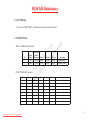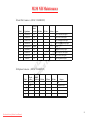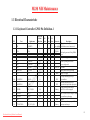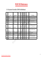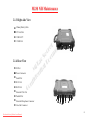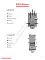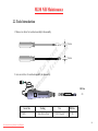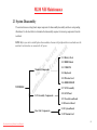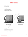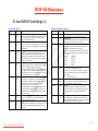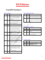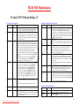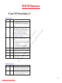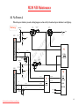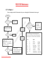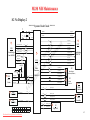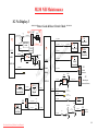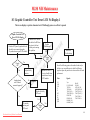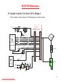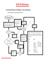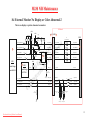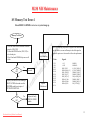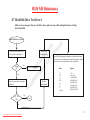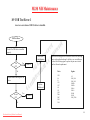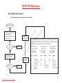
1
SERVICE MANUAL FOR M230 BY: Sanny Gao Technical Maintenance Department /GTK MTC Nov.2006 / R01 Downloaded from LpManual.com Manuals M230 N/B Maintenance Contents 1. Hardware Engineering Specification …………………………………………………………………… 4 1.1 Introduction ……………………………………………………………………………………………………………. 4 1.2 System Architecture ………………………………………………………………..…………………………………. 1.3 Electrical Characteristic ……...……………………………………………………………………………………….. 10 t t n e e r c m e u S c c Do a iT ial M t n e id f n o C 2. System View and Disassembly ………………………………………………………………………….. 2.1 System View ……………………………………………………………………………………………………………. 83 91 91 2.2 Tools Introduction …………………………………………………………………………………………………..…. 94 2.3 System Disassembly ……………………………………………………………………………………………………. 95 3. Definition & Location of Connectors/Switches ………………………………………………………… 117 3.1 Mother Board ……….……………………………………………………………..…………………………………… 117 3.2 I/O Board ……………………………………………...………………………………………………………………… 119 3.3 LED Board ……………………………………………………………………………………………………………… 121 3.4 Touch Screen Board …………………………………………………………………………………………………… 122 3.5 Switch Board …………………………………………………………………………………………………………… 124 4. Definition & Location of Major Components ………………………………………………………….. 126 4.1 Mother Board …………………………………………………………………………………………………..……… 126 5. Pin Description of Major Component …….……………………………………………………………. 128 5.1 Intel Yonah Processor CPU ……..……………………………………………………………………………………. 128 5.2 Intel 945GM North Bridge ……………………………………………………………………………………………. 133 1 Downloaded from LpManual.com Manuals M230 N/B Maintenance Contents 5.3 Intel ICH7-M South Bridge …………………………………………………………………………………………… 139 6. System Block Diagram …………………………………………………………………………………… 150 t t n e e r c m e u S c c Do a iT ial M t n e id f n o C 7. Maintenance Diagnostics ………………………………………………………………………………… 151 7.1 Introduction ……………………………………………………………………………………………………………. 151 7.2 Maintenance Diagnostics ……………………………………………………………………………………………… 7.3 Error Codes ……………………………………………………………………………………………………………. 152 153 8. Trouble Shooting ………………………………………………………………………………………… 160 8.1 No Power ………………………………………………………………………………………………………………. 162 8.2 No Display ……………………………………………………………………………………………………………… 8.3 Graphic Controller Test Error LCD No Display ……………………………………………………………………. 8.4 External Monitor No Display or Color Abnormal ….. ……………………………………………………………… 8.5 Memory Test Error ………………………………………….………………………………………………………… 8.6 Keyboard (K/B) or Touch Pad (T/P) Test Error ……………..…………………………………………………...… 8.7 Hard Disk Drive Test Error ………………………..…………………………………………………………………. 8.8 CD-ROM Test Error …………………………………………………………………..……………………………..… 8.9 USB Port Test Error …………………………………………………………………………………………………… 8.10 Audio Test Error ………………………………………………………………………………………..…………….. 8.11 LAN Test Error ………………………………………………………………………………………………………. 8.12 1394B Test Error ……………………………………………………………………………………………………... 8.13 Mini Express (Wireless) Socket Test Error …………………………………………………………………………. 166 169 171 173 175 177 179 181 185 188 190 192 2 Downloaded from LpManual.com Manuals M230 N/B Maintenance Contents 8.14 PCMCIA Socket Test Error ……..……………………………………..………………………………………….… 194 9. Spare Parts List ………………………………………………………………………………………….. 196 t t n e e r c m e u S c c Do a iT ial M t n e id f n o C 10. System Exploded Views ………………………………………………………………………………... 212 11. Reference Material ………………………………………………………………………………….….. 219 3 Downloaded from LpManual.com Manuals M230 N/B Maintenance 1. Hardware Engineering Specification 1.1 Introduction 1.1.1 General Description t t n e e r c m e u S c o 1.1.2 System Overview MarketingcRequirement a D iT ial M t n e id f n o C This document describes the system hardware engineering specification for M230 portable notebook computer system. The M230 notebook computer is a new mainstream high performance thin and light notebook in the MiTAC notebook family. – The new M230 is ruggedized notebook, high-portability industrial computer. It can be used in the vehicle field and office. The notebook computer also can connect with a docking to extend the capability of I/O devices. The M230 will support the Intel Mobile Pentium M based on 65 nm technology – Yonah 1.66 GHz processor or 1.5 GHz (option) processor via the 479-ball Micro-FCBGA packages and an operating Front Side Bus speed of 667 MHz. The Intel 945GM north bridge chipset supports host system bus at 667 MHz, 2 slots of DDR2 SODIMM (400/533 MHz) 256 MB to 2 GB total, internal video controller support RGB, TV-out, SDVO and LVDS video interfaces and hub interface to south bridge ICH7-M. The Intel 82801GBM (ICH7-M) south bridge supports PCI 2.3 interface, integrated IDE (PATA) controller, integrated Serial ATA (SATA) controller, integrated USB hub 2.0 up to 8 ports, integrated LAN 10/100 Mbit/s, integrated Intel high definition controller (Azalia), LPC interface, SMBus 2.0 interface, FWH interface, Real Time 4 Downloaded from LpManual.com Manuals M230 N/B Maintenance Clock (RTC), IRQ controller and advance programmable interrupt controller (APIC) support. On PCI Bus interface exist PCI1520 card-bus controller and TSB82AA2 1394B controller that supports PC cards and 1394B device separately, Wireless LAN on mini PCIE interface and X-BAY radio interface. On LPC interface exist super I/O that is SIO10N268. It provides four serial ports and one parallel port. The LPC will connect the Keyboard embedded controller H8S/2140 and flash memory for BIOS. t t n e e r c m e u S c c Do a iT ial M t n e id f n o C There are two SMBus interfaces, one is connected from ICH7-M and operating under master mode, the second is multi-master Bus and connected from H8S/2140. The Master provides interface to synthesizer and to memory identification. The multi-master channel used for thermal sensor controller (SMBus from LCD interface and SMBus from Docking). A CODEC (ALC260) with TI audio amplifier stereo analog audio to internal speakers, audio jack and docking. Digital audio-PDIF standard also provided to audio jack and to docking. System also provides LEDs to display system status, such as power on, battery state, HDD, Num Lock, Caps Lock and Scroll Lock. The system also provides a port to expand docking capability. Input/Output (I/O) ports can include parallel port, serial port, VGA port, USB, line out, video input. The system also provides DVD-ROM, Bluetooth, GPS, X-BAY radios. A full set of software drivers and utilities are available to allow advanced operating systems such as Windows 2000 and Windows XP to take full advantage of the hardware capabilities. Detailed specs as follow. 5 Downloaded from LpManual.com Manuals M230 N/B Maintenance Features CPU Standard: Intel Yonah processor LV dual core 1.66 GHz in µ-FCBGA package Intel Yonah processor LV dual core 1.5 GHz in µ-FCBGA package CPU thermal ceiling: 15 W FSB 667 MHz Core Logic L2 Cache System BIOS t t n e e r c m e u S c c Do a iT ial M t n e id f n o C Intel 945GM chipset (Calistoga) + ICH7-M (PCI Express x 6 channels) on-die 2 MB 1 MB flash EPROM Includes system BIOS (Phoenix solution, Kernel core version), VGA BIOS, plug & play, ACPI2.0 capability Boot from IDE & SATA devices, USB CD-ROM, USB FDD Suspend to DRAM/HDD PC2001 compliance Standard: 256 MB Memory Options: 512 MB/1 GB/2 GB (Max system memory of 2 GB in 2 slots) Supports 400/533 MHz DDR2 devices 2 DDR2 SO-DIMM (200-pin) - Integrated in 945GM chipset, Intel GMA950 graphic controller VGA Controller - Optional ATI M54-CSP VGA controller with 128 MB memory - Dual view function/LCD/CRT simultaneous display capability - 14.1" TFT XGA (1024 x 768) SPWG type 14.1" LCD Display - 15.0" TFT SXGA+ (1400 x 1050) SPWG type 15.0" LCD (Optional) Factory optional touch screen Factory option Hi-Contrast solution for 14" panel only Structure 3-spindle Video Memory Shared system memory 64 MB - Standard: Serial ATA 60 GB; up to 120 GB (5400 or 7200 rpm) HDD - Factory optional HDD heater for low temperature (-20 C~55 C) support - Optional low temperature 20 GB HDD without HDD heater 6 Downloaded from LpManual.com Manuals M230 N/B Maintenance Continue to the previous page - Built-in design to support operating mode free drop from 0 to 3 feet heigh HDD 1~3 feet: Protected by G-sensor 0~1 foot: Protected by special construction resistance design CD-ROM Bay Easy swappable bay for CD-ROM/COMBO Drive/DVD dual recorder/2nd battery - Water-proof membrane keyboard Keyboard - Factory optional water-proof rubber keyboard t t n e e r c m e u S c c Do a iT ial M t n e id f n o C - Factory optional back-light rubber keyboard Pointing Device PCMCIA Audio A sensitive control touch pad: capacitance type (Optional water-proof: resistance type) - Type II x 2 - Card Bus support - Type II x 1 and built-in smart card reader x 1 (optional) Azalia 32 bits 192 KHz/AC97' 2.3 Audio digital controllerBuild-in Stereo 2 W speakers - Serial port x 1 - USB 2.0 x 2 (USB power support maximum 1 A per port) - IrDA FIR x 1 - DC input x 1 - Docking Port (POGO pin, hot docking) compatible with M220 I/O Ports - CRT port x 1 - 1394B port x 1 (Optional: PS2 port x 1 ) - Parallel port x 1 - RJ-45 x 1 - RJ-11 x 1 - Microphone-in x 1 - Line-out x 1 - Integrated 10/100/1000 base-T Ethernet with TPM security function - Integrated 56 kbps Modem Communication - Integrated Wireless LAN (802.11 a/b/g) with antenna - Factory optional GPS module with antenna - Factory optional wireless module for GSM GPRS/CDMA with antenna 7 Downloaded from LpManual.com Manuals M230 N/B Maintenance Continue to the previous page Communication Cooling Battery AC Adaptor Dimensions Weight - Factory optional Bluetooth with antenna - No any interface between 4 antennas in the same time No fan - Main battery supports over 5 hours - Second battery supports over 2 hours (Based on system without M54 VGA controller) - 90 Watts universal or above, auto sensing/switching, fully support all the functions t t n e e r c m e u S c c Do a iT ial M t n e id f n o C - Input: 100-240 V, 50/60 Hz AC - 328 x 272.1 x 46 mm for M230-4 (14.1") - 338 x 286 x 46 mm for M230-5 (15") -Same dimension as M220 x1 (Front side) Software USB2.0, right side x 2, rear side x 2 Environmental Standard (Main System) IEC 68-2-1,2,14 / MIL-STD-810F, Method 501.4, 502.4 o Temperature o o Operating: 0 C to 55 C (standard)-W/O battery pack > 50 C o o o -20 C to 60 C (optional)-W/O battery pack > 50 C o o Storage: -40 C to 70 C Humidity Altitude According to IEC 68-2-30/MIL-STD-810F, Method 507.45% to 95% RH, non-condensing According to IEC 68-2-13/MIL-STD-810F, Method 500.4 Operating: 15,000 ft, non-operating: 40,000 ft Altitude change rate: 2,000 ft/min According to IEC 68-2-27/MIL-STD-810F, Method 516.5 Shock Operating: 15 g, 11 ms, half sine wave Non-operating: 50 g, 11 ms, half sine wave According to IEC 68-2-6 / MIL-STD-810F, Method 514.5 Operating: 10~57.5 Hz/0.075 mm, 57.5~500 Hz/1.0 g Vibration MIL-STD-810F, 514.5C1-high way truck vibration exposure Non-operating: 10~57.5 Hz/0.15 mm, 57.5~500 Hz/2.0 g MIL-STD-810F-514.5C-17 general minimum integrity exposure 8 Downloaded from LpManual.com Manuals M230 N/B Maintenance Continue to the previous page According to IEC 68-2-32 / MIL-STD-810F, Method 516.5 Drop - 3-foot-high free drop on steel plate, 4-foot-high free drop on plywood plate - 26 times/one machine (Panel close/Power off) According to IEC1000-4-2 Air Discharge: 0 KV~8 KV (included), no any error ESD t t n e e r c m e u S c c Do a iT ial M t n e id f n o C 8 KV~15 KV, allow soft error Contact data pin discharge: 0 KV~6 KV (included), no any error Salt Fog * 6 KV~ 8 KV, allow soft error 5% Sodium Chloride (NaCl) during the entire exposure period measure the salt fog fallout rate and PH of the fallout solution at least at 48-hour intervals. Ensure the fallout is 2 Regulation between 1 and 3 ml/80 cm /hr FCC part 15, Subpart B, C, Class B, UL, CUL, TUV, CE! , CB, CCC, WHQL, BSMI, E-Mark Removable Options: Easy changeable wireless modem in X-BAY: EDGE, EVDO, GPS ODD devices (Combo drive, DVD dual) Vehicle docking board (Backward compatible with M220) Options Factory Options: HDD heater Full travel membrane keyboard with backlight Rubber keyboard with backlight Blue tooth (class1) - TECOM Class I module BT3014 with Broadcom firmware v1.2 9 Downloaded from LpManual.com Manuals M230 N/B Maintenance 1.2 System Architecture 1.2.1 Function Description 1.2.1.1 CPU t t n e e r c m e u S c c Do a iT ial M t n e id f n o C Intel Mobile Yonah processor • First dual core processor for mobile (Yonah and Yonah low voltage skus) • 667 MT/s (667 MHz) FSB support • On-die, primary 32-KB instruction cache and 32-KB write back data cache • On-die, 2 MB L2 cache with advanced transfer cache architecture • Streaming SIMD Extension 2 (SSE2) and Streaming SIMD Extension 3 (SSE3) • Support Intel architecture with dynamic execution • Advanced gunning transceiver logic (AGTL+) bus driver technology • Enhanced Intel SpeedStep technology to anable real-time dynamic switching between multiple voltage and frequency points • Data prefetch logic • 479-ball Micro-FCBGA package 10 Downloaded from LpManual.com Manuals M230 N/B Maintenance 1.2.1.2 North Bridge & 3D Graphics DDR2 Chipset – Intel 945GM FSB Support • AGTL+bus driver technology with integrated GTL termination resister (gated AGTL+receivers for reduced power) t t n e e r c m e u S c c Do a iT ial M t n e id f n o C • Supports 32-bit AGTL+host bus addressing • 667 MT/s (667 MHz) and 533 MT/s (533 MHz) FSB support • 2X address, 4X data • Host bus dynamic bus inversion HDINV support • 12 deep, in-order queue Integrated System Memory DRAM Controller • Supports up to two DDR2 SDRAM channels (64 bit wide per channel) • One SO-DIMM connecter per channel • Maximum of two, double-sided unbuffered SO-DIMMs (4 rows populated) • Minimum amount of memory supported is 128 MB (16 MB x 16-b x 4 devices x 1 row=128 MB), using 256 MB technology Serial ATA controller • 256 MB, 512 MB and 1 GB technology using X8 and X16 devices • Three memory channel organization are supported for DDR2 11 Downloaded from LpManual.com Manuals M230 N/B Maintenance - Single channel - Dual channel symmetric - Dual channel asymmetric • Support DDR2 400/533/667 devices • Supports On-Die Termination (ODT) for DDR2 t t n e e r c m e u S c c Do a iT ial M t n e id f n o C • Supports fast chip select mode • Supports partial writes to memory using Data Mask signals (DM) • Supports high-density memory package for DDR2 type devices • Supports Reduced Power DDR2 (RPDDR2) • Supports Intel Rapid Memory Power Management External Graphics Using PCI Express Architecture Interface • One X16 (16 lanes) PCI Express port intended for graphics attach; fully compliant to the PCI Express base specification revision 1.0a • Maximum theoretical realized bandwidth on interface of 4 GB/s in each direction simultaneously, for an aggregate of 8 GB/s when X16 • Automatic discovery, negotiation and training of link out of set • Supports traditional PCI style traffic (asynchronous snooped, PCI ordering) • Supports traditional AGP style traffic (asynchronous non-snooped, PCI-X ordering) 12 Downloaded from LpManual.com Manuals M230 N/B Maintenance • Hierarchical PCI-compliant configuration mechanism for downstream devices (i.e. normal PCI 2.3 configuration space as a PCI-to-PCI bridge) • Supports lane reversal and bit swapping Internal Graphics Controller t t n e e r c m e u S c c Do a iT ial M t n e id f n o C • Graphics core frequency - 2D Display core frequency at 133, 200 or 250 MHz @ Vcc=1.05 V depending on the host/ memory configurations - 3D Render core frequency at 133, 166, 250 MHz @Vcc=1.05 V depending on the host/ memory configurations - Intel® Smart 2D Display Technology - Intel® dual-frequency graphics technology support - Dynamic Video Memory Technology (DVMT) 3.0 support • 3D graphics engine - DirectX* 9.0 support - OpenGL* 1.5 and 2.0 support - Zone rendering 2.0 support • Analog CRT DAC interface support - Supports max DAC frequency up to 400 MHz 13 Downloaded from LpManual.com Manuals M230 N/B Maintenance - 24-bit RAMDAC support - DDC2B compliant - Up to 2048x1536 resolution support • Analog TV-out interface support t t n e e r c m e u S c c Do a iT ial M t n e id f n o C - Integrated TV-out device supported on display pipes A and B - NTSC/PAL encoder standard formats supports - 480i/480p/576i/576p/720p/1080i/1080p modes supported - Tri-level Sync signal - Multiplexed output interface - Composite video with S-Video - S-Video - Component video - Up to 1024x768 resolution supported for NTSC/PAL - Macrovision, overscan scaling and flicker filtering support • Serial Digital Video out Port (SDVO) interface support - Two SDVO ports are muxed with a subset of the external graphics interface using PCI Express architecture signals - Each SDVO port support display pixel rates up to 200 MP/s (600 MB/s) 14 Downloaded from LpManual.com Manuals M230 N/B Maintenance - Supports a variety display devices such as DVI, TV-out, LVDS .etc - Supports hot plug and display - Support for HDCP SDVO devices - Support for Macrovision on SDVO TV-out devices - Support for lane reversal t t n e e r c m e u S c c Do a iT ial M t n e id f n o C • Digital LVDS interface support - Integrated dual channel LVDS interface supported on display pipe B only - Compliant with ANSI/TIA/EIA-644-2001 spec - Supports 25 MHz to 112 MHz single/dual channel LVDS LCD interface with support for format of 1x18 bpp for TFT panels with single channel LVDS, 2x18 bpp for TFT panels with dual channels LVDS - Panel fitting, panning and center mode supported - Spread Spectrum Clocking (SSC) supported - Panel power sequencing compliant with SPWG timing specification - Integrated PWM or dedicated GMBus interface for LCD backlight inverter control - Intel® Display Power Savings Technology 2.0 support - Maximum UXGA panel size supported - Maximum WUXGA wide panel size supported 15 Downloaded from LpManual.com Manuals M230 N/B Maintenance • PCI Express x1 port support - One general purpose PCI Express port support - External graphics using PCI Express architecture and SDVO are functional in this mode • Direct Media Interface (DMI) t t n e e r c m e u S c c Do a iT ial M t n e id f n o C - Chip-to-chip interconnect between the GMCH and Intel 82801GBM - DMI X2 and DMI X4 configurations support - Bit swapping is supported - Lane reversal is supported • Packing/power - 1466-ball micro-FCBGA (37.5 mm x 37.5 mm) with a 42-mil x 34-mil ball pitch - VCC (1.05 core supply) - VCCSM (DDR2=1.8 V I/O supply) - VCCHV (3.3 V high voltage supply) VCCA_CRTDAC (2.5 V CRT analog supply) VCC_SYNC (2.5 V HSYNC/VSYNC supply) - VCCD LVDS (1.5 V digital supply) VCCTX_LVDS (2.5 V Data/CLK Tx power supply) VCCA_LVDS (2.5 V LVDS analog supply) 16 Downloaded from LpManual.com Manuals M230 N/B Maintenance - VCCA_TVBG (3.3 V TV DAC bnad gap supply) VCCD_TVDAC (1.5 V TV DAC supply) VCCDQ_TVDAC (1.5 V TV DAC quiet supply) VCCA_TVDACA (3.3 V TV-out Channel A supply) VCCA_TVDACB (3.3 V TV-out Channel B supply) VCCA_TVDACC (3.3 V TV-out Channel C supply) t t n e e r c m e u S c c Do a iT ial M t n e id f n o C - VCC3G (1.5 V PIC-E/DMI analog supply) VCC3A_GBG (2.5V PCI-E/DMI band gap supply) - VCCA_HPLL (1.5 V host VCO supply) VCCA_MPLL (1.5 V system memory VCO) VCCD_HMPLL (1.5 V digital dividers supply) VCCA_3GPLL (1.5 V PCI-E PLL supply) VCCA_DPLLA/B (1.5 V Display A/B PLL supply) 17 Downloaded from LpManual.com Manuals M230 N/B Maintenance 1.2.1.3 System Frequency Synthesizer – ICS9LPR310 • ICS9LPR310 is a low power CK410M-compliant clock specification. This clock synthesizer provides a single chip solution for next generation P4 Intel processors and Intel chipsets. ICS9LPR310 is driven with a 14.318 MHz crystal 667 MT/s (667 MHz) FSB support • Supports tight ppm accuracy clocks for Serial-ATA and PCIEX t t n e e • r c m e • u S c c Do • a iT ial • M t n e 1.2.1.4 PCMCIA Controller idTI PCI 1520+TPS2224A f n o C • Supports programmable spread percentage and frequency Uses external 14.318 MHz crystal, external crystal load caps are required for frequency tuning PEREQ# pins to support PCIEX power management Programmable watchdog safe frequency Low power differential clock outputs (No 50 ohm resistor to GND needed) – TI PCI 1520 – Card Bus Controller • The PCI1520, a dual-slot Card Bus controller designed to meet the PCI Bus power management interface specification for PCI to Card Bus bridges, is an ultra-low power high-performance PCI-to-Card Bus controller that supports two independent card sockets compliant with the PC card standard • The PCI1520 provides features that make it the best choice for bridging between PCI and PC cards in both 18 Downloaded from LpManual.com Manuals M230 N/B Maintenance notebook and desktop computers. The 1997 PC card standard retains the 16-bit PC card specification defined in PCI local bus specification and defines the new 32-bit PC card, Card Bus, capable of full 32-bit data transfers at 33 MHz. The PCI1520 supports any combination of 16-bit and Card Bus PC cards in the two sockets, powered at 5 V or 3.3 V, as required • The PCI1520 is compliant with the PCI local bus specification and its PCI interface can act as either a PCI master device or a PCI slave device. The PCI bus mastering is initiated during Card Bus PC card bridging transactions. The PCI1520 is also compliant with PCI bus power management interface specification • Key Features t t n e e r c m e u S c c Do a iT ial M t n e id f n o C - 209-terminal MicroStar BGA ball-grid array (GHK/ZHK) package - 2.5 V core logic and 3.3 V I/O with universal PCI interfaces compatible with 3.3 V 5 V PCI signaling environments - Integrated low-dropout voltage regulator (LDO-VR) eliminates the need for an external 2.5 V power supply - Mix-and-match 5 V/3.3 V 16-bit PC cards and 3.3 V Card Bus cards - Two PC card or Card Bus slots with hot insertion and removal - Serial interface to TI TPS222X dual-slot PC card power switch - Burst transfers to maximize data throughput with Card Bus cards - Interrupt configurations: parallel PCI, serialized PCI, parallel ISA and serialized ISA - Serial EEPROM interface for loading subsystem ID and subsystem vendor ID - Pipelined architecture greater than 130 Mbps throughout from Card Bus-to-PCI and from PCI-to-Card Bus 19 Downloaded from LpManual.com Manuals M230 N/B Maintenance TPS2224A – PCMCIA and Card Bus Power Switch • The TPS2224A Card Bus power-interface switch provide an integrated power management solution for two PC card sockets. These devices allow the controlled distribution of 3.3 V, 5 V, 12 V to each card slot. The current-limiting and thermal protection features eliminate the need for fuses. Current-limiting reporting helps the user isolate a system fault. The switch Rds (on) and current-limiting values have been set for the peak and average current requirements stated in the PC card specification • key features t t n e e r c m e u S c c Do a iT ial M t n e id f n o C - Fast current limit response time - Fully integrated VCC and VPP switching for 3.3 V, 5 V and 12 V - Meets current PC card standards - VPP output selection independent of VCC - 12 V and 5 V supplies can be disabled - TTL-Logic compatible inputs - Short-circuit and thermal protection - 140 µA (Typical) quiescent current from 3.3 V input - Break-before-make switching - Power-on reset - 40 °C to 85 °C operating ambient temperature range - 32-pin SSOP package 20 Downloaded from LpManual.com Manuals M230 N/B Maintenance 1.2.1.5 Read Only Memory (Flash ROM) • FWH bus interface • Single 3.3 V operations • 3.3 V – volt Read • 3.3 V – volt Erase • 3.3 V – program t t n e e r c m e u S c c Do a iT ial M t n e id f n o C • Fast program operation • VPP=12 V • Byte-by-Byte programming: 9 µs (typ.) • Fast erase operation • Fast read access time: Tkg 11 ns • Endurance: 30 K cycles (typ.) • Twenty-year data retention • 16 even sectors with 64 K bytes • Any individual sector can be erased • Hardware protection • #TBL supports 64-Kbyte Boot Block hardware protection 21 Downloaded from LpManual.com Manuals M230 N/B Maintenance • #WP supports the whole chip except boot block hardware protection • Hardware features • Latched address and data • TTL compatible I/O • Automatic program and erase timing with internal VPP generation t t n e e r c m e u S c c Do a iT ial M t n e id f n o C • End of program or erase detection • Toggle bit • Data polling • Low power consumption • Read active current:15 mA (typ. for FWH mode) • VPP input pin • Acceleration (ACC) function accelerates program timing • Hardware reset pin (#RESET) • Reset the internal state machine to the read mode • Ready/#Busy output (RY/#BY) • Detect program or erase cycle completion • Dual BIOS function • Full-chip partition with 8 M-bit or dual-block partition with 4 M-bit 22 Downloaded from LpManual.com Manuals M230 N/B Maintenance • Available packages: 32L PLCC, 32L STSOP, 40L TSOP (10x20 mm), 32 PLCC lead free, 32L STSOP lead free and 40L TSOP (10x20 mm) lead free 1.2.1.6 Keyboard Controller The H8S/2140 is a high-speed central processing unit with an internal 32-bit architecture that is upwardcompatible with the H8/300 and H8/300H CPUs. The H8S/2000 CPU has sixteen 16-bit general registers, can address a 16-Mbyte linear address space and is ideal for real-time control. t t n e e r c m e u S c c Do a iT ial M t n e id f n o C Detail specification as below: Bus Controller • Basic bus interface • Burst ROM interface • Idle cycle insertion • Bus arbitration function Data Transfer Controller • Transfer is possible over any number of channels • Three transfer modes • One activation source can trigger a number of data transfers (chain transfer) • Direct specification of 16-Mbyte address space is possible 23 Downloaded from LpManual.com Manuals M230 N/B Maintenance • Activation by software is possible • Transfer can be set in byte or word units • A CPU interrupt can be requested for the interrupt that activated the DTC • Module stop mode can be set t t n e e r c m e u S c c Do a iT ial M t n e id f n o C 16-Bit Free-Running Timer (FRT) • Selection of four clock sources • Two independent comparators • Four independent input capture channels • Counter clearing • Seven independent interrupts • Special functions provided by automatic addition function 8-Bit PWM Timer (PWM) • Operable at a maximum carrier frequency of 625 KHz using pulse division (at 10 MHz operation) • Duty cycles from 0 to 100% with 1/256 resolution (100% duty realized by port output) • Direct or inverted PWM output and PWM output enable/disable control 24 Downloaded from LpManual.com Manuals M230 N/B Maintenance 14-Bit PWM Timer (PWMX) • Division of pulse into multiple base cycles to reduce ripple • Two resolution settings • Two base cycle settings t t n e e r c m e u S c c Do a iT ial M t n e id f n o C • Four operating speeds • Four operation clocks (by combination of two resolution settings and two base cycle settings) 8-Bit Timer (TMR) • Selection of clock sources • Selection of three ways to clear the counters • Timer output controlled by two compare-match signals • Cascading of TMR_0 and TMR_1 • Multiple interrupt sources for each channel Timer Connection • Five input pins and four output pins, all of which can be designated for phase inversion • An edge-detection circuit is connected to the input pins, simplifying signal input detection • TMR_X can be used for PWM input signal decoding 25 Downloaded from LpManual.com Manuals M230 N/B Maintenance • TMR_X can be used for clamp waveform generation Watchdog Timer (WDT) • Selectable from eight (WDT_0) or 16 (WDT_1) counter input clocks • Switchable between watchdog timer mode and interval timer mode t t n e e r c m e u S c c Do a iT ial M t n e id f n o C Serial Communication Interface (SCI & IrDA) • Choice of asynchronous or clocked synchronous serial communication mode • Full-duplex communication capability • The on-chip baud rate generator allows any bit rate to be selected • Choice of LSB-first or MSB-first transfer (except in the case of asynchronous mode 7-bit data) • Four interrupt sources Bus Interface (IIC) • Selection of addressing format or non-addressing format • Conforms to Philips I2Cbus interface (I2Cbus format) • Two ways of setting slave address (I2Cbus format) • Start and stop conditions generated automatically in master mode (I2C bus format) • Selection of the acknowledge output level in reception (I2C bus format) 26 Downloaded from LpManual.com Manuals M230 N/B Maintenance • Automatic loading of an acknowledge bit in transmission (I2C bus format) • Wait function in master mode (I2C bus format) • Wait function (I2C bus format) • Interrupt sources • Selection of 16 internal clocks (in master mode) t t n e e r c m e u S c c Do a iT ial M t n e id f n o C • Direct bus drive (SCL/SDA pin) • Automatic switching from formatless mode to I2C bus format (IIC_0 only) Host Interface X-Bus Interface • Control of the fast GATE A20 function • Shutdown of the XBS module by the HIFSD pin • Five host interrupt requests Keyboard Buffer Controller • Conforms to PS/2 interface specifications • Direct bus drive (via the KCLK and KD pins) • Interrupt sources: on completion of data reception and on detection of clock edge • Error detection: parity error and stop bit monitoring 27 Downloaded from LpManual.com Manuals M230 N/B Maintenance Host Interface LPC Interface (LPC) • Supports LPC interface I/O read cycles and I/O write cycles • Has three register sets comprising data and status registers • Supports SERIRQ t t n e e r c m e u S c c Do a iT ial M t n e id f n o C • Eleven interrupt sources A/D Converter • 10-bit resolution • Input channels: eight analog input channels and 16 digital input channels • Analog conversion voltage range can be specified using the reference power supply voltage pin (AVref) as an analog reference voltage • Conversion time: 13.4 µs per channel (at 10-MHz operation) • Two kinds of operating modes • Four data registers • Sample and hold function • Three kinds of conversion start • Interrupt request 28 Downloaded from LpManual.com Manuals M230 N/B Maintenance D/A Converter • 8-bit resolution • Two output channels • Conversion time: Max. 10 µs (when load capacitance is 20 pF) t t n e e r c m e u S c c Do a iT ial M t n e id f n o C • Output voltage: 0 V to AVref • D/A output retaining function in software standby mode I/O ports • Ten I/O ports (ports 1 to 6, 8, 9, A, and B), and one input-only port (port 7) Interrupt Controller • Two interrupt control modes • Priorities settable with ICR • Independent vector addresses • Thirty-one external interrupts • DTC control 29 Downloaded from LpManual.com Manuals M230 N/B Maintenance Power-Down Modes • Medium-speed mode • Subactive mode • Sleep mode t t n e e r c m e u S c c Do a iT ial M t n e id f n o C • Subsleep mode • Watch mode • Software standby mode • Hardware standby mode • Module stop mode 30 Downloaded from LpManual.com Manuals M230 N/B Maintenance 1.2.1.7 Super I/O – SMSC SIO10N268 3.3 Volt Operation (5 Volt Tolerant) PC99, PC01, ACPI 1.0 Compliant LPC Interface Design t t n e e r c m e u S c c Do a iT ial M t n e id f n o C X-Bus Interface (LPC Mode Only) • Three chip selects (Two I/O and one memory) • 8-Bit data transfers • Support for up to 2 MB flash • Interfaces with 3 V memory devices • Support for up to two external I/O components • Offers three modes of operation for I/O devices • Provides FWH emulation Serial IRQ Compatible with Serialized IRQ Support for PCI Systems Programmable Wake-up Event (PME) Interface 33 General Purpose Input/Output Pins System Management Interrupt 31 Downloaded from LpManual.com Manuals M230 N/B Maintenance 2.88 MB Super I/O Floppy Disk Controller • Licensed CMOS 765B floppy disk controller • Software and register compatible with SMSC's proprietary 82077AA compatible core • Supports two floppy drives directly • Configurable open drain/push-pull output drivers t t n e e r c m e u S c c Do a iT ial M t n e id f n o C • Supports vertical recording format • 16-byte data FIFO • 100% IBM compatibility • Detects All overrun and under run conditions • Sophisticated Power Control Circuitry (PCC) including multiple Power Down Modes for reduced power consumption • DMA enable logic • Data rate and drive control registers • 480 addresses, up to 15 IRQ and four DMA options Floppy Disk Available on Parallel Port Pins (ACPI Compliant) • Enhanced digital data separator • 2 Mbps, 1 Mbps, 500 Kbps, 300 Kbps, 250 Kbps data rates 32 Downloaded from LpManual.com Manuals M230 N/B Maintenance • Programmable precompensation Serial Ports • Four full function serial ports • High speed NS16C550 compatible UARTs with Send/Receive 16-byte FIFOs t t n e e r c m e u S c c Do a iT ial M t n e id f n o C • Supports 230 K and 460 K baud • Programmable baud rate generator • Modem control circuitry • 480 address and 15 IRQ options 33 Downloaded from LpManual.com Manuals M230 N/B Maintenance 1.2.1.8 1394B Controller – TI TSB82AA2 • Single 3.3 V supply (1.8 V internal core voltage with regulator) • 3.3 V and 5 V PCI signaling environments • Serial bus data rates of 100M bits/s, 200M bits/s, 400M bits/s and 800M bits/s t t n e e r c m e u S c c Do a iT ial M t n e id f n o C • Physical write posting of up to three outstanding transactions • Serial ROM or boot ROM interface supports 2-wire serial EEPROM devices • 33 MHz/64 bit and 33 MHz/32 bit selectable PCI interface • PCI burst transfers and deep FIFOs to tolerate large host latency • Transmit FIFO – 5 K asynchronous • Transmit FIFO – 2 K isochronous • Receive FIFO – 2 K asynchronous • Receive FIFO – 2 K isochronous • D0, D1, D2, and D3 power states and PME events per the PCI Bus power management interface specification • Programmable asynchronous transmit threshold • Isochronous receive dual-buffer mode • Out-of-order pipelining for asynchronous transmit requests • Register access fail interrupt when the PHY SYSCLK is not active 34 Downloaded from LpManual.com Manuals M230 N/B Maintenance • Initial bandwidth available and initial channels available registers • Digital video and audio performance enhancements • Fabricated in advanced low-power CMOS process • Multifunction terminal (MFUNC terminal 1) • PCI_CLKRUN protocol per the PCI Mobile Design Guide t t n e e r c m e u S c c Do a iT ial M t n e id f n o C • General-purpose I/O • CYCLEIN/CYCLEOUT for external cycle timer control for customized synchronization • Packaged in 144-terminal LQFP (PGE) 35 Downloaded from LpManual.com Manuals M230 N/B Maintenance 1.2.1.9 Audio Codec – Realtek ALC260 • Single-chip multi-bit Sigma-Delta converters with high S/N ratio • 1 stereo DAC supports 16/20/24-bit PCM format with 44.1/48/96/192 KHz sample rate • 2 stereo ADCs support 16/20-bit PCM format with 44.1/48/96 KHz sample rate t t n e e r c m e u S c c Do a iT ial M t n e id f n o C • Applicable for 2-Channel 192 KHz DVD-Audio solutions • LINE-OUT, HP-OUT, LINE1, LINE2, MIC1 and MIC2 are stereo input and output re-tasking • MONO line level output to subwoofer speaker for 2.1 channel applications • High-quality differential CD analog input • External PCBEEP input is applicable, and internal BEEP generator is integrated • Power-Off CD mode supported • Power management and enhanced power saving features • Power support: Digital: 3.3 V; Analog: 3.3 V/5.0 V • Selectable 2.5 V/3.75 V VREFOUT • Two jack detection pins (each designed to detect 4 jacks) • Supports 44.1 K/48 K/96 kHz/192 kHz S/PDIF output • Supports 44.1 K/48 K/96 KHz S/PDIF input • 48-pin LQFP packages (lead (Pb)-free package also available) 36 Downloaded from LpManual.com Manuals M230 N/B Maintenance • Supports external volume knob control • Reserve analog mixer architecture is backwards compatible with AC'97 • –64 dB ~ +30 dB with 1 dB mixer gain for fine volume control • Impedance sensing capability for each re-tasking jack • Built-in headphone amplifier for each re-tasking jack t t n e e r c m e u S c c Do a iT ial M t n e id f n o C • Supports GPIOs (General purpose input/output) for customized applications • Hardware copyright protection for DVD-Audio • Meets Microsoft WHQL/WLP 2.0 audio requirements • EAX™ 1.0 & 2.0 compatible • Direct Sound 3D™ compatible • A3D™ compatible • I3DL2 compatible • HRTF 3D positional audio • Emulation of 26 sound environments to enhance gaming experience • 10-band software equalizer • Voice cancellation and key shifting in Karaoke mode • Enhanced configuration panel and device sensing wizard to improve user experience • Content copy protection for S/PDIF interface 37 Downloaded from LpManual.com Manuals M230 N/B Maintenance • Power management setting • Microphone Acoustic Echo Cancellation (AEC) and Beam Forming (BF) technology for voice application • Mono/Stereo Microphone noise suppression t t n e e • r c m e u S • c c o a • D iT ial M t 1.2.1.11 Mobility VGA Chipsete –n ATI M54CSP128 id f n o C 1.2.1.10 LAN – Broadcom BCM5752 Integrates TPM 1.2 security functionality enabling OEMs to offer this high level of PC security as a standard feature Enables TPM-ready security platforms for next Microsoft OS (Longhorn) Integrates 10/100/1000 BASE-T transceiver and media access controller The M54/M52 provides the fastest and most advanced 2D, 3D and multimedia graphics performance for notebooks. The M54/M52 supports Shader Model 3.0, advanced memory interface technology, a brand new display controller and a consumer electronics (CE) quality TV (NTSC/PAL) encoder. The M54 is based on PCI Express technology and leverages a brand new graphics architecture. Based on 90 nm micron process technology, the M54 will deliver a 16-lane PCI Express bus interface and lead-free ASIC Features in Detail: 38 Downloaded from LpManual.com Manuals M230 N/B Maintenance 2D Acceleration Features • A highly optimized 128 bit engine, capable of processing multiple pixels/clock • Hardware acceleration is provided for Bitblt, line drawing, polygon and rectangle fills, bit masking, monochrome expansion, panning and scrolling, scissoring, and full ROP support (including ROP3) • Optimized handling of fonts and text using ATI proprietary techniques t t n e e r c m e u S c c Do a iT ial M t n e id f n o C • Game acceleration including support for Microsoft's DirectDraw: Double Buffering, Virtual Sprites, Transparent Blit, and Masked Blit • Acceleration in 8/15/16/32 bpp modes • Support for WIN 2000 & WIN XP GDI extensions: Alpha BLT, Transparent BLT, Gradient Fill • Hardware cursor support up to 64x64x32 bpp, with alpha channel for direct support of WIN 2000 & WIN XP alpha cursor standard 3D Acceleration Features • DirectX9 Shader Model 3.0 support • Full DX9 conformance, including floating point per component at full speed • Support for 2X AA, 4X AA and 6X AA subsamples, with little performance loss in most cases • Advanced AA quality algorithms, generating visuals that are superior to other solutions with an equivalent number of samples • 2X/4X/8X/16X anisotropic filtering modes. Adaptive algorithm with bi-linear (performance) and tri-linear (quality) options 39 Downloaded from LpManual.com Manuals M230 N/B Maintenance • Dedicated geometry acceleration for Direct3D and OpenGL, which incorporates 2 parallel Vector/Scalar Engines performing HW transformation, clipping and lighting • 2 full vertex processors in the VAP (Vertex Assembler & Processor) Motion Video Acceleration Features t t n e e r c m e u S c c Do a iT ial M t n e id f n o C • Video scaling and fully programmable YCrCb to RGB color space conversion for full-screen/full-speed video playback and fully adjustable color controls • Hardware I2C • VIP 2.0 with multi channel DMA transfer • Front end scaler support for 8, 15, 16, and 32 bpp color depths • Back end overlay/scaler supports up to 8x4 tap filtering, and always ensures at least 4x2 tap filtering even in extreme cases. 4x4 tap is typical. Back-end scaler also supports upscaling and downscaling, filtered scaling of all supported YUV formats, RGB32 and RGB15/16, and filtered display of images up to 1536 pixels wide • MPEG-4 simple profile suppor • Adaptive de-interlacing filter eliminates video artifacts caused by displaying interlaced video on noninterlaced displays, by analyzing image and using optimal de-interlacing function on a per-pixel basis Dual Display Features • Improved 64-bit display controller with symmetric display capabilities • Two triple 10-bit palette DACs (DAC and DAC2) with gamma correction for true WYSIWYG color. Pixel 40 Downloaded from LpManual.com Manuals M230 N/B Maintenance rates up to 400 MHz standard • Dual RGB CRT output • One C Y COMP output plus second RGB CRT output from second DAC • Dual displays (LCD/DVI, DVI/CRT, LCD/TV, CRT/TV, etc.), with completely independent resolution, refresh rates, h/w icon & h/w cursor and display data t t n e e r c m e u S c c Do a iT ial M t n e id f n o C • Hardware cursor up to 64x64 pixels in 2 bpp, full color AND/XOR mix and full color 8-bit alpha blend • Primary display supports VGA and accelerated modes, video overlay and hardware cursor • Secondary display supports TV-out or CRT. It supports accelerated modes, video overlay, and hardware cursor; however, it does not support VGA. Modes supported include 800x600 and 16:9 modes such as 848x480, with user flexibility for moving and sizing the screen MPEG-4 simple profile support • Support for up to 4 K x 4 K resolution display Digital Display Support • Support for fixed resolution displays (e.g. panels) from VGA (640x480) to wide UXGA (1920x1200) resolution with full ratiometric expansion ability for source modes up to 1400 x 1050 with standard display timing, or up to 1920x1440 with reduced blanking timing. Higher resolution panels and digital CRTs may be possibly supported-contact ATI for details • Improved auto expansion • Optional auto-centering mode to display desktop at native size without ratiometric expansion • Support for VGA text modes in centering panel modes (up to approximately 165 MHz pixel frequency) 41 Downloaded from LpManual.com Manuals M230 N/B Maintenance • Support for reduced blanking intervals, as defined by VESA Bus Support Features • PCI Express 1.0a and PCI Express 1.1 compliant. PCI Express is the latest generation I/O interconnect architecture which replaces conventional PCI and AGP buses in new PC platforms. Refer to PCI-SIG for specifications relating to PCI Express architecture t t n e e r c m e u S c c Do a iT ial M t n e id f n o C • Native X16 PCI Express bus interface • Supports X1, X2, X4, X8, X12 and X16 lane widths • Supports X16 lane reversal where the receiver on lanes 0 to 15 on the graphics endpoint are mapped to the transmitter on lanes 15 down to 0 on the root complex • Supports X16 lane reversal where the transmitter on lanes 0 to 15 on the graphics endpoint are mapped the receiver on lanes 15 down to 0 on the root complex (requires corresponding support on the root complex) • Supports X1, X2, X4, X8, X12 and X16 polarity inversion • Supports “Mobile Graphics Low-Power Addendum to the PCI Express Base Specification 1.0” Memory Support Features • 256/128/64-bit memory interface using DDR1 or DDR2 SDRAM/SGRAM or GDDR3 SDRAM (except M52-T) to build 16/32/64/128/256/512 MB configurations • Support for SSTL-1.8 memory interface 42 Downloaded from LpManual.com Manuals M230 N/B Maintenance Power Management Features • Single chip solution in 90 nm micron CMOS technology • Full ACPI 1.0b, OnNow, and IAPC (Instantly Available PC) power management • Static and Adynamic Power Management support (APM as well as ACPI) with full VESA DPM and energy star compliance t t n e e r c m e u S c c Do a iT ial M t n e id f n o C • Full PowerPlayTM 6.0, including enhanced Power on Demand support • The chip power management support logic supports four device power states - on, standby, suspend and off - defined for the OnNow architecture. Each power state can be achieved by software control bits • Clocks to every major functional block are controlled by a unique dynamic clock switching technique which is completely transparent to the software. By turning off the clock to the block that is idle or not used at that point, the power consumption is significantly reduced during normal operation Internal LVDS Spread Spectrum Support • The M54/M52 spread spectrum controller is capable of generating a triangular frequency modulation profile. The amount of spread and the modulation frequency is fully programmable • Only the LVDS display is available to be spread (i.e., 1 PLL) External Spread Spectrum Support • Memory and/or core clock spread spectrum support via the GPIO16 pin • External spread spectrum supported for TMDS or LVDS transmitters via the GENERICC/GENERICD pin 43 Downloaded from LpManual.com Manuals M230 N/B Maintenance PC Design Guide Compliance • Fully compliant with Windows Logo program requirements for all target Operating Systems. This includes both the current Logo requirements and the future (draft) requirements that will be enforced during the lifespan of the product • Fully compliant with Mobile PCI rev 1.0 t t n e e r c m e u S c c Do a iT ial M t n e id f n o C • Bi-endian support for compliance on a variety of processor platforms Test Capability Features • Full scan implementation on the digital core logic which provides high fault coverage through ATPG (Automatic test pattern generation vectors) • Dedicated test logic for the on-chip custom memory macros to provide complete coverage on these modules • A JTAG test mode (which is largely compliant with the IEEE 1149.1 standard) including internal scan chain for access to chip-level test functions and for board level connectivity testing • Integrated hardware diagnostic tests performed automatically upon initialization • High quality components through built-in scan and chip diagnostics • Improved access to the analog modules and PLLs in the M54/M52 in order to allow full evaluation and characterization of these modules Other Features 44 Downloaded from LpManual.com Manuals M230 N/B Maintenance • Support for serial ROM video BIOS • Support for 32 and 64-bit operating systems based on Intel, AMD and PowerPC CPUs • HW cursor support for monochrome, color and alpha blended cursors • GDI support for Alpha & Transparent BLTs, as well as Gradient Fills t t n • e e r c m e u S c 1.2.1.12 USB Bluetooth (option) TECOM BT3014 c o a D • iT ial M t • n • e id • f n o C • Compliance with Wassenaar Agreement 3D vector rate (as defined by the Wassenaar Agreement) is 58-78 M 10-pixel vectors/sec – Bluetooth Specification V.1.2 compliant Bluetooth spec 1.1 compatible Bluetooth protocol stacks and profiles support is optional Indoor coverage range up to 50 m typically in general environments for the Class 1 output power with 0dBi omni-directional antenna Outdoor coverage range up to 100 m typically in open site for the Class 1 output power with 0dBi omnidirectional antenna • Output power controllable • Max data rate 720 kbps 45 Downloaded from LpManual.com Manuals M230 N/B Maintenance 1.2.1.13 Fax/Modem – Askey 1456VQL-T1 (INT-LF) • HD audio, AC’97, MC’97 2.2 compliant • V.44, V.42, V.42bis and MNP ™ Class 5 data compression • Low-power standby mode t t n e e r • c m e • u S c c Do • a iT ial M t 1.2.1.14 South Bridge ICH7-M n e id f n • o C • 3.3 V to 5 V power supply • Compliant with FCC, CTR21, JATE and other PTTs Auto sensing host interface to select AC’97 or HD audio OperationtTemperature/humidity: 0 °C/0%~60 °C/90% Storage temperature/humidity: -20 °C/0%~70 °C/90% PCI Bus Interface Supports PCI Revision 2.3 Specification at 33 MHz • Supports up to 6 master devices on PCI • NEW: Six available PCI REQ/GNT pairs • Support for 64-bit addressing on PCI using DAC protocol 46 Downloaded from LpManual.com Manuals M230 N/B Maintenance PCI Express Interface • 4 PCI Express root ports • NEW: 2 Additional PCI Express root ports (Not available on all ICH7 SKUs) • Supports PCI Express 1.0a t t n e e r c m e u S c c Do a iT ial M t n e id f n o C • Ports 1-4 can be statically configured as 4x1,or 1x4 • Support for full 2.5 Gb/s bandwidth in each direction per x1 lane • Module based Hot-Plug supported (e.g., Express Card) Integrated Serial ATA Host Controller • two ports (Mobile Only) • Integrated AHCI controller (Not available on all ICH7 SKUs) Integrated IDE Controller • Independent timing of up to two drives • Ultra ATA 100/66/33, BMIDE and PIO modes • Tri-state modes to enable swap bay USB2.0 47 Downloaded from LpManual.com Manuals M230 N/B Maintenance • Includes four UHCI host controllers that support eight external ports • Includes one EHCI high-speed USB 2.0 host controller that supports all eight ports • Includes one USB 2.0 High-speed debug port • Supports wake-up from sleeping states S1-M–S5 • Supports legacy keyboard/mouse software t t n e e r c m e u S c c Do a iT ial M t n e id f n o C Intel® High Definition Audio Interface • PCI Express endpoint • Independent Bus Master logic for eight general purpose streams: four input and four output • Support three external Codecs • Supports variable length stream slots • Supports multichannel,, 32-bit sample depth, 92 KHz sample rate output • Provides mic array support • Allows for non-48 KHz sampling output • Support for ACPI device states • NEW: Docking support • NEW: Low voltage mode 48 Downloaded from LpManual.com Manuals M230 N/B Maintenance Interrupt Controller • Support up to eight PCI interrupt pins • Supports PCI 2.3 message signaled interrupts • Two cascaded 82C59 with 15 interrupts • Integrated I/O APIC capability with 24 interrupts t t n e e r c m e u S c c Do a iT ial M t n e id f n o C • Supports processor system bus interrupt delivery 1.05 V operation with 1.5 V and 3.3 V I/O • 5V tolerant buffers on IDE, PCI, USB over-current and legacy signals Timers Based on 82C54 • System timer, refresh request, speaker tone output Power Management Logic • ACPI 2.0 compliant • ACPI-defined power states (C1–C4, S1-M, S3–S5) • ACPI power management timer • Support for “Intel® SpeedStepTM technology” processor power control • Support for “Deeper Sleep” power state 49 Downloaded from LpManual.com Manuals M230 N/B Maintenance • PCI CLKRUN# and PME# support • SMI# generation • All registers readable/restorable for proper resume from 0 V suspend states • Support for APM-based legacy power management for non-ACPI Desktop and Mobile implementation t t n e e r c m e u S c c Do a iT ial M t n e id f n o C External Glue Integration • Integrated pull-up, pull-down and series termination resistors on IDE, processor interface • Integrated Pull-down and Series resistors on USB NEW: Serial Peripheral Interface(SPI) for Serial and Shared Flash Firmware Hub (FWH) Interface supports BIOS memory size up to 8 MB Low Pin Count (LPC) Interface • Supports two Master/DMA devices • Support for Security Device(Trusted Platform Module) connected to LPC Enhanced DMA Controller • Two cascaded 8237 DMA controllers • Supports LPC DMA 50 Downloaded from LpManual.com Manuals M230 N/B Maintenance Real-Time Clock • 256-byte battery-backed CMOS RAM • Integrated oscillator components • Lower Power DC/DC Converter implementation t t n e e r c m e u S c c Do a iT ial M t n e id f n o C System TCO Reduction Circuits • Timers to generate SMI# and Reset upon detection of system hang • Timers to detect improper processor reset • Integrated processor frequency strap logic • Supports ability to disable external devices SMBus • Flexible SMBus/SMLink architecture to optimize for ASF • Provides independent manageability bus through SM-Link interface • Supports SMBus 2.0 Specification • Host interface allows processor to communicate via SMBus • Slave interface allows an internal or external microcontroller to access system resources • Compatible with most two-wire components that are also I2C compatible 51 Downloaded from LpManual.com Manuals M230 N/B Maintenance NEW: 1.05 V Core Voltage Integrated 1.05 V Voltage Regulator (INTVR) for the Suspend and LAN wells GPIO: TTL, open-drain, inversion Package 31x31 mm 652 mBGA t t n e e r c m e u S c c Do a iT ial M t n e id f n o C 52 Downloaded from LpManual.com Manuals M230 N/B Maintenance 1.2.1.15 LED Indicators There are 13 LED indicators locate on the system housing, the detail shows on the follows table: LED Number Functions LED color Remark LED BD HD1 Power on/Suspend Green/Red Power on: Green LED on, Suspend: Red LED on. LED BD HD2 LED BD HD4 LED BD HD5 LED BD HD3 M/BD D34 M/BD D33 M/BD D32 M/BD D35 M/BD D36 M/DB D37 M/BD D836 M/BD D31 HDD Amber If HDD in accessing, LED on Num Lock Green Keyboard Number Lock Caps Lock Green Keyboard Caps Lock Scroll Lock Green Keyboard Scroll Lock CDROM Amber If ODD in accessing, LED on Battery Low Battery Charge Status Wireless LAN Amber If battery in Low state, amber LED blinks. If AC exist, amber LED on when battery in charging, Green LED on if battery full. When wireless LAN link, Green LED on. If GPRS module exist, green LED on, and amber LED on if the module active. If the Ethernet LAN link, amber LED on, and green LED on if the Ethernet LAN active. If Touch Pad disable, LED on If AC exists, Green LED on. If HDD temperature below 2°C or ambient temperature over 60°C, Red LED blinks. t t n e e r c m e u S c c Do a iT ial M t n e id f n o C Amber /Green Green XBAY GPRS module Amber /Green LAN Amber /Green Touch Pad ON/Off green AC IN/HDD Low Temp. Green/Red 53 Downloaded from LpManual.com Manuals M230 N/B Maintenance 1.2.1.16 Mini PCI-E Interface • Mechanical dimension support the Mini Card • Mini PCI_E Interface – Pin out of System Connector Pin 1 3 5 7 9 11 13 15 17 19 21 23 25 27 29 31 33 35 37 39 41 43 45 47 49 51 53 Signal PCIE_WAKE# WLAN_AACTIVE BT_ACTIVE PCIECLKREQ2# GROUND CLK_PCIE_S1# CLK_PCIE_S1 GROUND TP TP GROUND PCIE_RXN3 PCIE_RXP3 GROUND GROUND PCIE_TXN3 PCIE_TXP3 GROUND NC NC NC NC NC NC NC NC GROUND Pin 2 4 6 8 10 12 14 16 18 20 22 24 26 28 30 32 34 36 38 40 42 44 46 48 50 52 54 Signal 3.3VS GROUND 1.5VS NC NC NC NC NC GROUND MINI_PD# BUF_PLT_RST# 3.3V GROUND 1.5VS SMBCLK SMBDATA GROUND NC NC GROUND S1_LED0 S1_LED1 S1_LED2 1.5VS GROUND 3.3V GROUND t t n e e r c m e u S c c Do a iT ial M t n e id f n o C 54 Downloaded from LpManual.com Manuals M230 N/B Maintenance 1.2.1.17 Buttons • Power on (I/O BD: HSW1) – Push button for power on and off control 1.2.1.18 I/O Ports t t n e e r c m e u S c c Do a iT ial M t n e id f n o C RJ-11 Modem Line Connector Pin 1 2 Signal Name TIP Power On default Direction Active S0 State Active S3 State Active RING Active Active Active S4 State Power off Description Transmit Data Tip Power off Transmit Data Ring RJ-45 With LED Connector Pin 1 g Name TX+ default OD S0 State S3 State S4 State Description Data Transmit and Receive 2 TX- OD Data Transmit and Receive 3 RX+ OD Data Transmit and Receive 4 TRD2+ OD Data Transmit and Receive 5 TRD2- OD Data Transmit and Receive 6 RX- OD Data Transmit and Receive 7 TRD3+ OD Data Transmit and Receive 8 TRD3- OD Data Transmit and Receive 55 Downloaded from LpManual.com Manuals M230 N/B Maintenance Infrared Interface Supporting IRDA Format -HSDL 3602 (288003602002) • Fully compliant to IrDA 1.1 physical layer specifications (9.6 Kb/s to 4 Mb/s operation) • Typical link distance of =1.0 m • Low power operation of 3.3 V t t n e e r c m e u S c c Do a iT ial M t n e id f n o C • Small module size of height 4.0 mm, width 12.2 mm, depth 5.1 mm • Complete shutdown (TXD, RXD, PIN Diode) • Low shutdown current of 10 nA typical • Single Rx data output allowing speed select by FIR select pin • Excellent noise immunity with integrated EMI Shield • Edge detection input feature preventing the LED from long turn-on time • Interface to various super I/O and controller devices • Designed to accommodate light loss with Cosmetic Window 56 Downloaded from LpManual.com Manuals M230 N/B Maintenance Pin 1 Signal Name VCC Power On default Direction Power off S0 State +3V S3 State Chip Power off S4 State Power off Description Supply Voltage Ground Ground Ground Ground Analog Ground 2 AGND 3 FIR_SEL In Out Chip Power off Power off FIR Select 4 MD0 In Out Chip Power off Power off Mode 0 5 MD1 In Out Chip Power off Power off Mode 1 6 NC 7 GND Ground Ground 8 RXD In 9 TXD 10 LEDA t t n e e r c m e u S c c Do a iT ial M t n e id f n o C Ground Ground Ground In Chip Power off Power off Receiver Data OUT OUT Chip Power off Power off Transmitter Data OUT OUT Chip Power off Power off LED Anode USB Ports-FOXCONN USB113C – K1 (MiTAC 331040004039) Pin # Signal Description 1 USB1_5V default 0V S0 State 5V S3 State 5V S4 State 5V 2 USB1- Low I/O Low Low Supply voltage USB Differential Data Minus 3 USB1+ Low I/O Low Low USB Differential Data Plus 4 GND Ground Ground Ground Ground Ground Antenna Switch Connector (MiTAC 297150100015) • It passes antenna signal from system to docking for using vehicle dock 57 Downloaded from LpManual.com Manuals M230 N/B Maintenance POGO Docking Port Connector – (MiTAC 796115000001) Pin # Signal name 1 VDOCK_POGO 2 DVMAIN_POGO 3,4,6 5 Ground P_H8_SM_DATA default S0 State S3 State S4 State In, 19V In In In OUT, 19V OUT OUT OUT Ground Ground Ground Ground Hi-Z I/O I/O Hi-Z Description Support mother board and battery charge Support docking board Ground SMBus Data t t n e e r c m e u S c c Do a iT ial M t n e id f n o C 8 P_H8_SM_CLK Hi-Z I/O I/O Hi-Z SMBus Clock 7 P_USB5+ Low I/O Low Low USB Differential Data Plus 10 P_USB5- Low I/O Low Low USB Differential Data Minus 9 P_DOCK_RI# I 11 P_SPDIFOUT O SPIDFOUT Signal 12 P_USBOC#5 I USB over current to USB HUB 13 P_USB4+ 16 P_USB4- 14 P_SUSB# 15 +3V_POGO 17,18 +5V_POGO Ring indicator Low I/O Low Low USB Differential Data Plus Low I/O Low Low USB Differential Data Minus Out, 3.3V Out, 3.3V Out, 3.3V Out, 5V Out, 5V Out, 5V O S3 control Out, 3.3V +3,3V POWER Out, 5V +5V POWER 19 POGO_DOCK_IN I Dock sense 20 P_PWRON_CARKEY I Ignition input 21 +5VA_POGO 22 AGND 23 P_MIC 24 P_AOUT_L 25 P_AOUT_R Out, 5V Out, 5V Out, 5V Out, 5V Supply voltage Ground Ground Ground Ground Ground I Microphone Input Signal O Line Out Left Signal O Line Out Right Signal 58 Downloaded from LpManual.com Manuals M230 N/B Maintenance Serial Port Connector – (MiTAC 331040009005) Pin # Signal name Power On default Direction 1 COM1DCD# IN COM1 Carrier detector signal 2 COM1RXD IN COM1 Received data signal 3 COM1TXD O COM4 Transmitted data signal COM1 Data terminal ready signal S0 State S3 State S4 State Purpose t t n e e r c m e u S c c Do a iT ial M t n e id f n o C 4 COM1DTR# O 5 Shield-ground Ground 6 COM1DSR# IN COM1 Data set ready signal 7 COM1RTS# O COM1 Request to send signal 8 COM1CTS# IN COM1 Clear to send signal 9 COM1RI# IN COM1 Ring indicator signal Ground Micphone Connector – (MiTAC 331040005015) Pin # 1 2 3 4 5 Signal name GND Mic in Power On default Direction S0 State S3 State S4 State Purpose GND Microphone Input NC NC NC 59 Downloaded from LpManual.com Manuals M230 N/B Maintenance Parallel Port Connector – (MiTAC 331040009005) Pin # Signal name Power On default Direction S0 State S3 State S4 State Purpose 1 P_STB# O 2 P_LPD0 I/O PIO Strobe 3 P_LPD1 I/O PIO Data bit1 signal 4 P_LPD2 I/O PIO Data bit2 signal 5 P_LPD3 I/O PIO Data bit3 signal 6 P_LPD4 I/O PIO Data bit4 signal 7 P_LPD5 I/O PIO Data bit5 signal 8 P_LPD6 I/O PIO Data bit6 signal PIO Data bit0 signal t t n e e r c m e u S c c Do a iT ial M t n e id f n o C 9 P_LPD7 I/O 10 D/ACK# I PIO Printer Acknowledge PIO Data bit7 signal 11 D/BUSY I PIO Printer Busy 12 D/PE I PIO Printer Paper End 13 D/SLCT I PIO Printer Selected Status 14 D/AFD# O PIO Auto Feed 15 D/ERR# I PIO Printer Error 16 D/INIT# O PIO Printer Initiate 17 D/SLIN# 18,19,20,21,2 Shield2,23,24,25 ground I PIO printer Select Input Ground Ground 60 Downloaded from LpManual.com Manuals M230 N/B Maintenance VGA Port Connector – (Mitac 331040009005) Pin # Signal name Power On default Direction S0 State S3 State S4 State Purpose 1 CRT_RED CRT RED SIGNAL 2 CRT_GREEN CRT GREEN SIGNAL 3 CRT_BLUE CRT BLUE SIGNAL 4 NC No Connect 5 Ground 6 Ground 7 Ground 8 Ground 9 NC 10 Ground 11 NC 12 CRT_DDCDATA CRT DDC Data Signal 13 CRT_HSYNC CRT Horizontal Synchronization 14 CRT_VSYNC CRT Vertical Synchronization 15 CRT_DDCCLK CRT DDC Clock Signal t t n e e r c m e u S c c Do a iT ial M t n e id f n o C Ground Ground Ground Ground No Connect Ground No Connect 61 Downloaded from LpManual.com Manuals M230 N/B Maintenance 1394B Port Connector (MiTAC 291000000905) Pin # Signal name Power On default Direction S0 State S3 State S4 State Purpose 1 TPB0- I/O Differential signal 2 TPB0+ I/O Differential signal 3 TPA0- I/O Differential signal 4 TPA0+ 5 Shield-ground Ground 6 Shield-ground Ground 7 NC No Connection 8 VCC 9 Shield-ground t t n e e r c m e u S c c Do a iT ial M t n e id f n o C I/O Differential signal 19V Ground Stereo Jack – (MiTAC 331840010019) Pin # 1 Signal name DECT HP#/OPT 2 Line out left 3 Line out right 4 AGND Power On default Direction S0 State S3 State S4 State Purpose Audio and Optical Fiber Device detect Audio Line out left signal Audio Line out right signal Audio ground 5 Device detect 6 NC Audio Device detect 7 SPDIFOUT Optical Fiber 8 VCC 3V 9 GND Ground 10 NC No Connection No Connection 62 Downloaded from LpManual.com Manuals M230 N/B Maintenance 1.2.1.19 Internal Connector Definition LCD Connector (MiTAC 291000005017)-1 Pin # Signal name 1 LCDVCC default O 2 LCDVCC O S0 State S3 State Purpose S4 State 3 V with fuse controlled by EN VDD video 3 V with fuse controlled by EN VDD video t t n e e r c m e u S c c Do a iT ial M t n e id f n o C 3 LCDVCC 4 +5V 5 GND 6 TXCLK- 7 TCCLK+ 8 GND 9 TXOUT0- 10 TXOUT0+ 11 GND 12 TXOUT1- 13 TXOUT1+ 14 GND 15 TXOUT2- 16 TXOUT2+ 17 GND 18 BLADJ 19 EN_BKL 20 +5V 21 O 3 V with fuse controlled by EN VDD video O +5 V GND Ground O Sampling Clock (Positive : -) O Sampling Clock (Negative : +) GND Ground O Transmission Data of Pixels 0 (Negative : -) O Transmission Data of Pixels 0 (Positive : +) GND Ground O Transmission Data of Pixels 1 (Negative : -) O Transmission Data of Pixels 1 (Negative : +) GND Ground O Transmission Data of Pixels 2 (Negative : -) O Transmission Data of Pixels 2 (Negative : +) GND Ground O Adjust LCD Brightness Signal O Enable backlight O support to inverter +5V O support to inverter 22 COM3_RTS# O COM3 Request to send signal 23 COM3_TXD O COM3 Transmitted data signal 24 COM3_RXD O COM3 Received data signal 63 Downloaded from LpManual.com Manuals M230 N/B Maintenance Continue to the previous page Pin # Signal name 25 Power On S0 State S3 State S4 State Purpose DDCPCLK O 27 DDCPDATA USBP7- O O Low Low Low DDC Data USB Differential Data Minus 28 USBP7+ O Low Low Low USB Differential Data Plus 29 +5V 30 +5V 31 DVMAIN 32 DVMAIN 33 +3V 34 +3V 35 +3V 36 26 DDC Clock t t n e e r c m e u S c c Do a iT ial M t n e id f n o C O Supply to touch screen controller O Supply to touch screen controller O support to inverter O support to inverter O +3 V O +3 V O +3 V COM3_DTR# O COM3 Data terminal ready signal 37 LCD_SM_DATA O For SM bus GPIO controller 38 LCD_SM_CLK O For SM bus GPIO controller 39 GND 40 TXOUTB0- 41 TXOUTB0+ 42 GND 43 TXOUTB1- O Transmission Data of Pixels 1 (Negative : -) 44 TXOUTB1+ O Transmission Data of Pixels 1 (Negative : +) GND O O GND GND Ground Transmission Data of Pixels 0 (Negative : -) Transmission Data of Pixels 0 (Positive : +) Ground 45 GND 46 TXOUTB2- O Transmission Data of Pixels 2 (Negative : -) 47 TXOUTB2+ O Transmission Data of Pixels 2 (Negative : +) 48 GND GND Ground Ground 49 TXCLKB- O Sampling Clock (Positive : -) 50 TCCLKB+ O Sampling Clock (Negative : +) 64 Downloaded from LpManual.com Manuals M230 N/B Maintenance KBD Connector (MiTAC 291000003015) Pin # 1 Signal name KI7 Power On default Direction I S0 State S3 State S4 State Purpose KBD matrix 2 KI6 I KBD matrix 3 KI5 I KBD matrix 4 KI4 I KBD matrix 5 KI3 I KBD matrix 6 KI2 I KBD matrix 7 KI1 I KBD matrix 8 KI0 I KBD matrix 9 KO15 O KBD matrix 10 KO14 O KBD matrix 11 KO13 O KBD matrix 12 KO12 O KBD matrix 13 KO11 O KBD matrix 14 KO10 O KBD matrix 15 KO9 O KBD matrix 16 KO8 O KBD matrix 17 KO7 O KBD matrix 18 KO6 O KBD matrix 19 KO5 O KBD matrix 20 KO4 O KBD matrix 21 KO3 O KBD matrix 22 KO2 O KBD matrix 23 KO1 O KBD matrix 24 KO0 O KBD matrix t t n e e r c m e u S c c Do a iT ial M t n e id f n o C 65 Downloaded from LpManual.com Manuals M230 N/B Maintenance Continue to the previous page Pin # Signal name Power On default Direction O S0 State S3 State S4 State Purpose 25 GND Ground 26 EL_VB O EL lamp drive 27 EL_VB O EL lamp drive 28 EL_VA O EL lamp drive 29 EL_VA O EL lamp drive 30 LED_KB_PWR O LED keyboard power t t n e e r c m e u S c c Do a iT ial M t n e id f n o C SATA HDD Connector (MiTAC 291000025204) Pin # 1-4 Signal name +19V_HEAT Power On default Direction S0 State S3 State S4 State Purpose O Heater Power 5 HDD_D- Remote Thermal Negative Input 6 HDD_D+ Remote Thermal Positive Input 7 TEMP_SEN I Temperature Sense 8 +5VA O Power Supply 9,10,12 +5VS O Power Supply 25 SATAHDD_TXN O SATA Differential Signal 26 SATAHDD_TXP O SATA Differential Signal 29 SATAHDD_RXN I SATA Differential Signal 30 11,13,18,34-52 14-17,19-24, 27,28,31-33 SATAHDD_RXP GND I GND SATA Differential Signal Ground NC 66 Downloaded from LpManual.com Manuals M230 N/B Maintenance RTC Battery Connector 2-pin Hirose DF13-2P (MiTAC 291000020233) Pin # 1 2 Signal name +3VA Power On default Direction O GND GND S0 State S3 State S4 State Purpose t t n e e r c m e u S c c Do a iT ial M t n e id f n o C • The charge function will not support for RTC battery • The consumption of RTC CMOS memory will be ~3 uA, the calculated life cycle for the RTC battery is no less than 6 years PCMCIA Connector (MiTAC 291000251504) Pin No Pin Name 72 B_CAD0 Direction S0 State S3 State S4 State Description 70 B_CAD1 71 B_CAD2 68 B_CAD3 69 B_CAD4 65 B_CAD5 66 B_CAD6 63 B_CAD7 62 B_CAD8 58 B_CAD9 Card Bus address/data bus 60 B_CAD10 Card Bus address/data bus Card Bus address/data bus Card Bus address/data bus Card Bus address/data bus Card Bus address/data bus Card Bus address/data bus Card Bus address/data bus Card Bus address/data bus Card Bus address/data bus Card Bus address/data bus 67 Downloaded from LpManual.com Manuals M230 N/B Maintenance Continue to the previous page Pin No Pin Name Direction S0 State S3 State S4 State Description 56 B_CAD11 Card Bus address/data bus 54 B_CAD12 Card Bus address/data bus 55 B_CAD13 Card Bus address/data bus 52 B_CAD14 Card Bus address/data bus 53 B_CAD15 Card Bus address/data bus 50 B_CAD16 30 B_CAD17 29 B_CAD18 28 B_CAD19 27 B_CAD20 24 B_CAD21 22 B_CAD22 20 B_CAD23 18 B_CAD24 15 B_CAD25 13 B_CAD26 11 B_CAD27 10 B_CAD28 8 B_CAD29 7 B_CAD30 5 B_CAD31 61 B_CCBE0# 49 B_CCBE1# 31 B_CCBE2# 16 B_CCBE3# t t n e e r c m e u S c c Do a iT ial M t n e id f n o C Card Bus address/data bus Card Bus address/data bus Card Bus address/data bus Card Bus address/data bus Card Bus address/data bus Card Bus address/data bus Card Bus address/data bus Card Bus address/data bus Card Bus address/data bus Card Bus address/data bus Card Bus address/data bus Card Bus address/data bus Card Bus address/data bus Card Bus address/data bus Card Bus address/data bus Card Bus address/data bus Card Bus bus commands and byte enables. Card Bus bus commands and byte enables. Card Bus bus commands and byte enables. Card Bus bus commands and byte enables. 68 Downloaded from LpManual.com Manuals M230 N/B Maintenance Continue to the previous page Pin No Pin Name Direction S0 State S3 State S4 State Description 47 B_CPAR Card Bus bus parity 45 B_CPERR# Card Bus parity error indicator 42 B_CGNT# Card Bus bus grant 40 B_CINT# Card Bus interrupt 34 B_CIRDY# Card Bus initiator ready 4 B_CCLKRUN# Card Bus clock run 73 Card Bus detect 1 Cars Bus voltage sense 1 and Card Bus detect 2 t t n e e r c m e u S c c Do a iT ial M t n e id f n o C 57,26 B_CCD1# B_CVS1, B_CVS2 46 B_CBLOCK# Card Bus lock 44 B_CSTOP# Cars Bus stop 41 B_CDEVSEL# Card Bus device select 35 B_CTRDY# Card Bus target ready 32 B_CFRAME# Card Bus cycle frame 23 B_CRST# Card Bus reset 21 B_CSERR# 19 B_CREQ# 14 B_CAUDIO Card Bus audio 12 B_CSTSCHG Card Bus states change 3 B_CCD2# Card Bus detect 1 36 B_CCLK 38,39 CARD_VB 6 B_RSVD/D2 48 B_RSVD/A18 64 B_RSVD/D14 37 VPPBOUT Card Bus system error Card Bus request Card Bus clock Switched output that delivers 0 V, 3.3 V, 5 V, or high impedance to card Switched output that delivers 0 V 3.3 V, 5 V, 12 V, or high impedance to card 69 Downloaded from LpManual.com Manuals M230 N/B Maintenance Continue to the previous page Pin No Pin Name 1,9,17,25,3 3,59,67,74, 75 GND Direction S0 State S3 State S4 State Description Ground 147 A_CAD0 Card Bus address/data bus 145 A_CAD1 Card Bus address/data bus 146 A_CAD2 143 A_CAD3 144 A_CAD4 140 A_CAD5 141 A_CAD6 138 A_CAD7 137 A_CAD8 133 A_CAD9 135 A_CAD10 Card Bus address/data bus 131 A_CAD11 Card Bus address/data bus 129 A_CAD12 Card Bus address/data bus 130 A_CAD13 Card Bus address/data bus 127 A_CAD14 Card Bus address/data bus 128 A_CAD15 Card Bus address/data bus 125 A_CAD16 Card Bus address/data bus 105 A_CAD17 Card Bus address/data bus 104 A_CAD18 Card Bus address/data bus 103 A_CAD19 Card Bus address/data bus 102 A_CAD20 Card Bus address/data bus 99 A_CAD21 Card Bus address/data bus 97 A_CAD22 Card Bus address/data bus 95 A_CAD23 Card Bus address/data bus 93 A_CAD24 Card Bus address/data bus t t n e e r c m e u S c c Do a iT ial M t n e id f n o C Card Bus address/data bus Card Bus address/data bus Card Bus address/data bus Card Bus address/data bus Card Bus address/data bus Card Bus address/data bus Card Bus address/data bus Card Bus address/data bus 70 Downloaded from LpManual.com Manuals M230 N/B Maintenance Continue to the previous page Pin No Pin Name Direction S0 State S3 State S4 State Description 90 A_CAD25 Card Bus address/data bus 88 A_CAD26 Card Bus address/data bus 86 A_CAD27 Card Bus address/data bus 85 A_CAD28 Card Bus address/data bus 83 A_CAD29 Card Bus address/data bus 82 A_CAD30 Card Bus address/data bus 80 A_CAD31 136 A_CCBE0# 124 A_CCBE1# 106 A_CCBE2# 91 A_CCBE3# Card Bus address/data bus Card Bus bus commands and byte enables. Card Bus bus commands and byte enables. Card Bus bus commands and byte enables. Card Bus bus commands and byte enables. 122 A_CPAR Card Bus bus parity 120 A_CPERR# t t n e e r c m e u S c c Do a iT ial M t n e id f n o C Card Bus parity error indicator 117 A_CGNT# Card Bus bus grant 115 A_CINT# Card Bus interrupt 109 A_CIRDY# Card Bus initiator ready 79 A_CCLKRUN# Card Bus clock run 148 132,101 A_CCD1# A_CVS1, A_CVS2 Card Bus detect 1 Cars Bus voltage sense 1 and Card Bus detect 2 121 A_CBLOCK# Card Bus lock 119 A_CSTOP# Cars Bus stop 116 A_CDEVSEL# Card Bus device select 110 A_CTRDY# Card Bus target ready 107 A_CFRAME# Card Bus cycle frame 71 Downloaded from LpManual.com Manuals M230 N/B Maintenance Continue to the previous page Pin No Pin Name Direction S0 State S3 State S4 State Description 98 A_CRST# Card Bus reset 96 A_CSERR# Card Bus system error 94 A_CREQ# Card Bus request 89 A_CAUDIO Card Bus audio 87 A_CSTSCHG Card Bus states change 78 A_CCD2# Card Bus detect 2 111 A_CCLK 113,114 CARD_VA t t n e e r c m e u S c c Do a iT ial M t n e id f n o C 81 A_RSVD/D2 123 A_RSVD/A18 139 A_RSVD/D14 112 VPPAOUT 76,77,84,9 2,100,108, 118,126,13 4,142,149, 150 GND Card Bus clock Switched output that delivers 0 V, 3.3 V, 5 V, or high impedance to card Switched output that delivers 0 V 3.3-V, 5-V, 12-V, or high impedance to card Ground 72 Downloaded from LpManual.com Manuals M230 N/B Maintenance I/O Board 28-pin Connector (Mitac 291000012806) Pin # 1-12 Signal name Power On default Direction NC Purpose S0 State S3 State S4 State Not Connect 19 COM1DCD# IN COM1 Carrier detector signal 15 COM1RXD IN COM1 Received data signal 27 COM1TXD O COM1 Transmitted data signal 23 COM1DTR# O COM1 Data terminal ready signal 21 COM1RI# IN COM1 Ring indicator signal 17 COM1DSR# IN COM1 Data set ready signal 13 COM1RTS# O COM1 Request to send signal 25 14 COM1CTS# MDI0+ IN I/O COM1 Clear to send signal Data Transmit and Receive 16 MDI0- I/O Data Transmit and Receive 18 MDI1+ I/O Data Transmit and Receive 20 MDI1- I/O Data Transmit and Receive 22 MDI2+ I/O Data Transmit and Receive 24 MDI2- I/O Data Transmit and Receive 26 MDI3+ I/O Data Transmit and Receive 28 MDI3- I/O Data Transmit and Receive t t n e e r c m e u S c c Do a iT ial M t n e id f n o C 73 Downloaded from LpManual.com Manuals M230 N/B Maintenance I/O Board 120-pin Connector (Mitac 291000011229)-1 Pin # Signal name default S0 State S3 State S4 State Purpose 1 AGND Analog Ground 2 DEVICE_DECT# Audio Device detect 3 SPDIFOUT S/PDIF OUT 4 GND Ground 5 LCD_SM_DATA For SM bus GPIO controller 6 LCD_SM_CLK For SM bus GPIO controller 7 DDCPCLK DDC Clock 8 DDCPDATA 9 COM3_RXD 10 COM3_TXD 11 COM3_RTS# 12 SUSB# 13-20 PIO_PD0-7 t t n e e r c m e u S c c Do a iT ial M t n e id f n o C DDC Data COM3 Received data signal COM3 Transmitted data signal COM3 Request to send signal S3 control PIO Data bit0~7 signal 21 PIO_STROBE# O PIO Strobe 22 PIO_ALF# PIO_ERROR# O PIO Auto Feed 23 24 PIO_INIT# 25 I PIO Printer Error O PIO Printer Initiate PIO_SLCTIN# I PIO printer Select Input 26 PIO_ACK# I PIO Printer Acknowledge 27 PIO_BUSY 28 PIO_PE 29 PIO_SLCT 30 LID# 31 COM3_DTR# I PIO Printer Busy I PIO Printer Paper End I PIO Printer Selected Status LID Function +5V COM3 Data terminal ready Power Supply 34 CRT_HSYNC CRT Horizontal Sync. Signal 35 CRT_VSYNC CRT Vertical Sync. Signal 32-33 74 Downloaded from LpManual.com Manuals M230 N/B Maintenance I/O Board 120-pin Connector (Mitac 291000011229)-2 Continue to the previous page Pin # Signal name 36 CRT_DDCCLK default S0 State S3 State S4 State Purpose CRT DDC Clock Signal 37 CRT_DDCDATA CRT DDC Data Signal 38 CRT_BLUE CRT BLUE Signal 39 CRT_GREEN 40 CRT_RED 41 USBP7- 42 USBP7+ 43 EN_BKL 44 BLADJ 45-47 LCD_+3VS 48 NC 49 GND 50 TXCLK- 51 TXCLK+ 52 GND 53 TXOUT0- 54 TXOUT0+ 55 GND 56 TXOUT1- CRT GREEN Signal t t n e e r c m e u S c c Do a iT ial M t n e id f n o C CRT RED Signal I/O USB Differential Data Minus I/O USB Differential Data Plus O Enable Backlight O Adjust LCD Brightness Signal O +3VS For LCD Not Connect GND Ground Sampling Clock (Positive : -) Sampling Clock (Positive : +) GND Ground Transmission Data of Pixels 0 (Negative : -) Transmission Data of Pixels 0 (Positive : +) GND Ground Transmission Data of Pixels 1 (Negative : -) 57 TXOUT1+ 58 GND 59 TXOUT2- 60 TXOUT2+ Transmission Data of Pixels 2 (Positive : +) 61,65 Transmission Data of Pixels 1 (Positive : +) GND GROUND Transmission Data of Pixels 2 (Negative : -) AGND Analog Ground 62 LINE_OUT_L Audio Line out left signal 63 LINE_OUT_R Audio Line out right signal 64 MIC Microphone Input Signal 66-81 KO0-15 Downloaded from LpManual.com Manuals O KBD matrix 75 M230 N/B Maintenance I/O Board 120-pin Connector (Mitac 291000011229)-3 Continue to the previous page Pin # Signal name 82-89 KI7-0 90 91 default I POWERSW# I S0 State S3 State S4 State Purpose KBD matrix Power Button KBD_EN_EL O Keyboard Enable EL 92-93 +3VS O Power Supply 94-95 +5VS O Power Supply 96-97 +3V O Power Supply 98-99 LCD_DVMAIN O Power Supply t t n e e r c m e u S c c Do a iT ial M t n e id f n o C 100 CRT_IN# 101 WLAN_ACTIVE 102 BT_ACTIVE 103-108 NC 109 GND 110 TXOUTB0- 111 TXOUTB0+ 112 GND 113 TXOUTB1- 114 TXOUB1+ 115 GND 116 TXOUTB2- 117 TXOUTB2+ 118 GND 119 TXCLKB- 120 TXCLKB+ I Indication for CRT IN O WLAN Communication with BT I BT Communication with WLAN Not Connect Ground Transmission Data of Pixels 0 (Negative : -) Transmission Data of Pixels 0 (Positive : +) Ground Transmission Data of Pixels 1(Negative : -) Transmission Data of Pixels 1(Positive : +) Ground Transmission Data of Pixels 2 (Negative : -) Transmission Data of Pixels 2 (Positive : +) Ground Sampling Clock (Positive : -) Sampling Clock (Positive : +) 76 Downloaded from LpManual.com Manuals M230 N/B Maintenance IDE 50-Pin Connector (MiTAC 291000025038 )-1 Power On default Direction S0 State Pin # Signal name 1 CD_R S3 State S4 State CD ROM Audio right Output Purpose 2 CD_L CD ROM Audio left Output 3 GND 4 CD_COMM Ground 5 IDE_PDD8 I/O 6 IDE_RESET I 7 IDE_PDD9 I/O IDE Device data 9 8 IDE_PDD7 I/O IDE Device data 7 9 IDE_PDD10 I/O IDE Device data 10 10 IDE_PDD6 I/O IDE Device data 6 11 IDE_PDD11 I/O IDE Device data 11 12 IDE_PDD5 I/O IDE Device data 5 13 IDE_PDD12 I/O IDE Device data 12 14 IDE_PDD4 I/O IDE Device data 4 15 IDE_PDD13 I/O IDE Device data 13 16 IDE_PDD3 I/O IDE Device data 3 17 IDE_PDD14 I/O IDE Device data 14 18 IDE_PDD2 I/O IDE Device data 2 19 IDE_PDD15 I/O IDE Device data 15 20 IDE_PDD1 I/O IDE Device data 1 21 IDE_PDDREQ I 22 IDE_PDD0 I/O I t t n e e r c m e u S c c Do a iT ial M t n e id f n o C CD ROM Audio ground IDE Device data 8 Reset DMA Request IDE Device data 0 23 IDE_PDIOR# 24-25 GND Read Strobe 26 IDE_PDIOW O Write Strobe 27 IDE_PDDACK# O DMA Acknowledge Ground 77 Downloaded from LpManual.com Manuals M230 N/B Maintenance IDE 50-Pin Connector (MiTAC 291000025038 )-2 Continue to the previous page Power On default Direction S0 State I Pin # Signal name 28 IDE_PIORDY 29 NC 30 IDE_IRQ14 O 31 CD_DIAG I/O 32 IDE_PDA1 O Address 1 33 IDE_PDA2 O Address 2 34 IDE_PDA0 O Address 0 35 IDE_PDCS#3 O Chip Select signal 36 IDE_PDCS#1 O Chip Select signal 38 CDACTP# 37 +5V + 5 volts power +5V + 5 volts power +5V + 5 volts power +5V + 5 volts power +5V + 5 volts power GND Ground GND Ground 39 40 41 42 43 44 45 46 47 48 S3 State S4 State Purpose I/O Ready Not Connect Interrupt signal t t n e e r c m e u S c c Do a iT ial M t n e id f n o C Passed Diagnostics Led driver NC Not Connect GND Ground GND Ground CSEL Master device 49 USBP1- I/O USB Differential Data Minus 50 USBP1+ I/O USB Differential Data Plus 78 Downloaded from LpManual.com Manuals M230 N/B Maintenance Speaker Left 2-pin Connector – HIROSE (MiTAC 291000020202) Pin # 1 2 Power On default Signal name Direction S0 State SPKLOUT+ 2W /4 ohm SPKLOUT- S3 State 2W /4 ohm S4 State Purpose Line out to speaker left Line out to speaker Left t t n e e r c m e u S c c Do a iT ial M t n e id f n o C PS2 Board 6-pin Connector (MiTAC 291000010630) Pin # Signal name Direction S0 State S3 State S4 State Purpose +5V POWER 1 +5V 2 M_CLK Mouse Clock 3 M_DATA Mouse Data 4 K_CLK Keyboard Clock 5 K_DATA Keyboard Data 6 GND Ground 79 Downloaded from LpManual.com Manuals M230 N/B Maintenance X-Bay 84-pin Connector – (Mitac 291000018402)-1 Pin # Signal name 1,3,5,7,9,11,13, NC 15,17,19,21,23, 29,31,33,35,37 2,4,6 Vsys 8,10,12 14,16 18,20 22,24 26 28 25,27 30 32 34 36 38 40 42 44 Power On default Direction S0 State S3 State S4 State Purpose Not Connect t t n e e r c m e u S c c Do a iT ial M t n e id f n o C O +19V +5V O +5V +3V O +3V +5VS O +5VS +3VS O +3VS +5VA O Always +5V +12V O +12V USB OC# I USB Over Current Signal USBP6- I/O Low Low Low USB Differential Data 6 Minus USBP6+ I/O Low Low Low USB Differential Data 6 Plus USBP3- I/O Low Low Low USB Differential Data 3 Minus USBP3+ I/O Low Low Low USB Differential Data 3 Plus PCIE_RXN2 I PCIE Signal PCIE_RXP2 I PCIE Signal PCIE_TXN2 O PCIE Signal PCIE_TXP2 O PCIE Signal 46 CLK_PCIE PCIE Signal 48 CLK_PCIE PCIE Signal 50 PCIECLKREQ# 52 PCIE_WAKE# PCIE Signal 54 PCI_RESET# PCI Signal I PCIE Signal 80 Downloaded from LpManual.com Manuals M230 N/B Maintenance X-Bay 84-pin Connector – (Mitac 291000018402)-2 Pin # 56 Signal name SMBCLK Power On default Direction S0 State S3 State S4 State Purpose SM BUS Clock signal 58 SMBDATA SMI BUS Data signal 62 MIC Microphone Input Signal LINEIN_L Audio Line out left signal LINEIN_R Audio Line out right signal CCRST SIM Card Reset Signal CCGND SIM Card Ground Signal CCIO SIM Card Serial Data Signal CCVCC SIM Card Power Signal CCVCC SIM Card Power Signal CCCLK SIM Card Clock Signal 66 70 74 76 78 80 82 84 t t n e e r c m e u S c c Do a iT ial M t n e id f n o C 39,41,43,45,47, GND 49,60,64,68,72 51 SUSB# 53 Ground S3 control XBAY_GPIO0 GPIO Signal XBAY_GPIO1 GPIO Signal XBAY_RX_YEL LED Control Signal XBAY_TX_GRN LED Control Signal XBAY_LINK LED Control Signal 63 XBAY_ACT LED Control Signal 65 XBAY_ID0 XBAY ID Select Signal 67 XBAY_ID1 XBAY ID Select Signal 69 COM4_TXD COM4 Transmitted data signal 55 57 59 61 81 Downloaded from LpManual.com Manuals M230 N/B Maintenance X-Bay 84-pin Connector – (Mitac 291000018402)-3 Pin # 71 73 75 77 79 81 83 Signal name COM4_RXD COM4_DTR# Power On default Direction S0 State S3 State S4 State Purpose COM4 Received data signal COM4 Data terminal ready signal t t n e e r c m e u S c c Do a iT ial M t n e id f n o C COM4_DCD# COM4 Carrier detector signal COM4_RTS# COM4 Request to send signal COM4_CTS# COM4_DSR# COM4 Clear to send signal COM4 Data set ready signal COM4_RI# COM4 Ring indicator signal 82 Downloaded from LpManual.com Manuals M230 N/B Maintenance 1.3 Electrical Characteristic 1.3.1 Keyboard Controller GPIO Pin Definition-1 Power On default Direction S0 State S3 State S4 State 8 /STBY/FVPP 9 VCC1 10 PA7/KEYIN15 11 PA6/KEYIN14 12 P52/SCK0 13 P51/RXD0 t t n e e r c m e u S c c Do a iT ial M t n e id f n o C 14 PIN Port 1 /RES 2 XTAL 3 EXTEL 4 VCCB 5 MD1 6 MD0 7 /NMI Signal name Connect to Description When pin low, the chip is Reset button reset/Hardware reset button used H8_RESET# I XTAL I Crystal EXTAL I Crystal Clock pulse generator/Using 10MHz input VCCB I VDD5 Always 5 V supply H8_MODE1 I H8_MODE0 I H8_SUSB I Set the operating mode/Mode 3 choose single mode ICH7-M H8_STBY# I VCC1 I VDD3 K_DATA O P/S 2 K_CLK O P/S 2 BAT_CLK_H8 I/O Battery USE_A I/O P50/TXD0 USE_B I/O 15 VSS4 VSS4 I GND 16 P97/WAIT/ SDA BAT_DATA_H8 I Battery S3 control standby mode/Always pull high Always 3V supply PA7 input and output pins/ ps2 keyboard data PA6 input and output pins/ ps2 keyboard clock input and output pins I2C bus clock input and output pins/I2C bus clock output pin GPIO/ Software control charger to main or second battery charging Ground I2C data input and output pins/I2C data input and output 83 Downloaded from LpManual.com Manuals M230 N/B Maintenance 1.3.1 Keyboard Controller GPIO Pin Definition-2 PIN Port Signal name Power On default Direction S0 State S3 State S4 State Connect to Description 17 P96/0 G_SENSOR# O G-sensor GPI/ HDD drop sensor interrupt pin 18 P95/AS H8_SB_PWRBTN# O ICH7-M GPIO/ ICH6 power button signal 19 P94/WR BAT_SM_SW O 20 PA5/KEYIN13 M_DATA O 21 PA4/KEYIN12 22 P93/RD 23 P92/IRQ0 24 P91/IRQ1/EIOW 25 P90/IRQ2/ESC2 26 P60/KEYIN0/FTC1 27 P61/KEYIN1/FTOA 28 P62/KEYIN2/FTIA 29 P63/KEYIN3/FTIB 30 PA3/KEYIB11 31 PA2/KEYIN10 32 P64/KEYIN4/FTIC 33 P65/KEYIN5/FTID 34 P66/KEYIN6/IRQ6 35 P67/KEYIN7/IRQ7 36 GPIO/ Software control SMBus switch PA5 input and output pins/ ps2 mouse data input and output pins PA4 input and output pins/ ps2 mouse clock input and output pins t t n e e r c m e u S c c Do a iT ial M t n e id f n o C P/S 2 M_CLK O P/S 2 H8_THRM# O ICH7-M H8_LID# I H8_POWERBTN# I H8_SUSC I ICH7-M KBD_KI0 I Keyboard Keyboard Matrix KBD_KI1 O Keyboard Keyboard Matrix KBD_KI2 I Keyboard Keyboard Matrix GPIO/ Throttle signal GPIO/ LID switch signal input pin Power switch GPIO/ Power button used S4 control KBD_KI3 I Keyboard Keyboard Matrix TPD_DATA O Touch Pad Touch Pad data TPD_CLK O Touch Pad Touch Pad clock KBD_KI4 I Keyboard Keyboard Matrix KBD_KI5 I Keyboard Keyboard Matrix KBD_KI6 O Keyboard Keyboard Matrix KBD_KI7 I Keyboard Keyboard Matrix AVREF AVREF I +3VA Always 3V supply 37 AVCC AVCC I +3VA 38 P70/AN0 VBATT1 I Battery1 Always 3V supply Analog input pin/Read main battery voltage 84 Downloaded from LpManual.com Manuals M230 N/B Maintenance 1.3.1 Keyboard Controller GPIO Pin Definition-3 PIN 39 Port Signal name Power On default Direction S0 State S3 State S4 State Connect to Description Analog input pin/Read second battery voltage P71/AN1 VBATT2 I Battery2 40 P72/AN2 WAKE_ON_LAN# I BCM5752 41 P73/AN3 SEN_DDR I +1.8V Analog input pin/Read 1.8V voltage 42 P74/AN4 SEN_3V I +3V Analog input pin/Read 3 V voltage 43 P75/AN5 SEN_VCORE I Vcore 44 P76/AN6/DA0 ISET I 45 P77/AN7/DA1 BLADJ I Inverter 46 AVSS AVSS I GND 47 PA1/KEYIN9 RING# O 48 PA0/KEYIN8 ADEN# O 49 P40/TMCI0 PWROK I ICH7-M 50 P41/TMO0 SPK_OFF O ALC260 51 P42/TMRI0 H8_SMB_DATA I 52 P43/TMCI1/HIRQ1 H8_SCI I ICH7-M 53 P44/TMO1/HIRQ1 USB_CTRL O MIC2545 54 P45/TMRI1/HIRQ1 POWERON CARKEY# I GPIO/ IGNITION signal power on 55 P46/PW0 PWR_ON O 56 P47/PW1 HDD_HEAT_PWM O GPIO/Output power on signal PWM D/A pulse output pin/HDD heater PWM output Wake from LAN t t n e e r c m e u S c c Do a iT ial M t n e id f n o C HDD Analog input pin/Read Vcore voltage Analog output pin/output charger current Analog output pin/LCD panel brightness Ground PA1 input and output pins/ Modem ring signal input PA0 input and output pins/ AC input signal GPIO/ Power OK signal output GPIO/Software control speaker on or off I2C bus data input and output pins/I2C bus data input and output pins GPIO/ SCI output pin GPIO/Software control device power on or off 85 Downloaded from LpManual.com Manuals M230 N/B Maintenance 1.3.1 Keyboard Controller GPIO Pin Definition-4 PIN Port 57 PB7/XDB7 58 PB6/XDB6 59 VCC2 60 P27/A15 61 P26/A14 62 P25/A13 63 P24/A12 64 P23/A11 65 P22/A10 66 P21/A9 67 P20/A8 68 PB5/XDB4 69 PB4/XDB4 70 VSS1 71 VSS2 72 P17/A7 73 P16/A6 Signal name LED_DATA Power On default Direction I/O S0 State S3 State S4 State Connect to LED Description PB7 input and output pins/ Output LED indicator data signal PB6 input and output pins/ Output LED indicator clock signal t t n e e r c m e u S c c Do a iT ial M t n e id f n o C LED_CLK I/O LED VCC2 I +3VA Always 3V supply KO15 KEY BD MATRIX : KO14 KEY BD MATRIX : KO13 KEY BD MATRIX : KO12 KEY BD MATRIX : KO11 KEY BD MATRIX : KO10 KEY BD MATRIX : KO9 KEY BD MATRIX : KO8 O Keyboard Internal Keyboard Internal Keyboard Internal Keyboard Internal Keyboard Internal Keyboard Internal Keyboard Internal Keyboard Keyboard Matrix O O O O O O O Keyboard Matrix Keyboard Matrix Keyboard Matrix Keyboard Matrix Keyboard Matrix Keyboard Matrix Keyboard Matrix ALERT I/O Battery LEARNING# I/O Battery VSS1 I GND Ground VSS2 KEY BD MATRIX : KO7 KEY BD MATRIX : KO6 I GND Internal Keyboard Internal Keyboard Ground O O PB5 input p and output p ppins disable AC function Keyboard Matrix Keyboard Matrix 86 Downloaded from LpManual.com Manuals M230 N/B Maintenance 1.3.1 Keyboard Controller GPIO Pin Definition-5 PIN Port 74 P15/A5 75 P14/A4 76 P13/A3 77 P12/A2 78 P11/A1 79 P10/A0 80 PB3/XDB3 81 PB2/XDB2 82 P30/HDB0/D0 83 P31/HDB1/D1 84 P32/HDB2/D2 85 P33/HDB3/D3 Power On default Direction S0 State S3 State S4 State O Connect to Internal Keyboard Internal Keyboard Internal Keyboard Internal Keyboard Internal Keyboard Internal Keyboard BAT2_IN# I/O Battery RCIN# I/O ICH7-M LPC_LAD0 I/O LPC_LAD1 I/O LPC_LAD2 I/O LPC_LAD3 I/O Signal name KEY BD MATRIX : KO5 KEY BD MATRIX : KO4 KEY BD MATRIX : KO3 KEY BD MATRIX : KO2 KEY BD MATRIX : KO1 KEY BD MATRIX : KO0 O Description Keyboard Matrix t t n e e r c m e u S c c Do a iT ial M t n e id f n o C O O O O Keyboard Matrix Keyboard Matrix Keyboard Matrix Keyboard Matrix Keyboard Matrix PB3 input and output pins/second battery plug in signal PB2 input and output pins/ Reset CPU signal LPC command, address, data input and output pins/LPC address and data input and output 86 P34/HDB4/D4 FRAME# I/O The start of an LPC cycle or forced termination of an abnormal LPC cycle/LPC frame 87 P35/HDB5/D5 PLT_RST# I/O LPC reset/LPC reset 88 P36/HDB6/D6 PCI_H8_CLK I/O Clock 89 P37/HDB7/D7 SERIRQ I/O ICH7-M LPC clock input pin/LPC clock Input and output pin for LPC serialized host interrupts/LPC serial host interrupts 87 Downloaded from LpManual.com Manuals M230 N/B Maintenance 1.3.1 Keyboard Controller GPIO Pin Definition-6 PIN 90 Port PB1/XDB1 Signal name Power On default Direction S0 State S3 State S4 State Connect to Description DOCK_IN# I/O Docking I/O ICH7-M I GND Ground IDE_HDD_PWR I/O HDD A20GATE I/O ICH7-M PCI_CLKRUN I/O PCI device LPC_PD# I/O GPIO/ HDD power on or off A20 gate control signal output pin/A20 gate used Input and output pins that requests the start of LCLK operation when LCLK is stopped/LCLK function used Input pin that controls LPC module shutdown/controls LPC module shutdown 91 PB0/XDB0 EXTSMI# 92 VSS3 VSS3 93 P80/HA0 94 P81/GA20 95 P82/CLKRUN# 96 P83/PLCPD# 97 P84/IRQ2/TXD1 98 P85/IRQ4/RXD1 99 P86/IRQ5/SCK1 100 /RESO LSCI output pin/ Dock in signal input LSMI output pin/SMI output pin t t n e e r c m e u S c c Do a iT ial M t n e id f n o C H8_WAKE_UP# I GPIO/Wakeup event RSMRST# I H8_SMB_CLjK I Resume reset I2C bus clock input and output pins/I2C bus clock output pin N/A O 88 Downloaded from LpManual.com Manuals M230 N/B Maintenance 1.3.2 ICH7-M GPIO Pin Definition-1 Item Multi. Func./Note Signal Name / Description 0 PM_BMBUSY# GPIO0 1 PCI_REQ5#(Reserved) 2 PCI_INTE# 3 PCI_INTF# 4 Power On default Direction S0 State S3 State S4 State Power plane I Low Low Core GPIO1/REQ5# I Low Low Core GPIO2/PIRQE# I Off Off Core GPIO3/PIRQF# I Off Off Core PCI_INTG# GPIO4/PIRQG# I Off Off Core 5 PCI_INTH# GPIO5/PIRQH# I Off Off Core 6 GPO_ENOVA GPIO6 I Off Off Core 7 SCI# GPIO7 I Off Off Core 8 EXTSMI# GPIO8 I Driven Driven Resume t t n e e r c m e u S c c Do a iT ial M t n e id f n o C 9 SUSPEND# GPIO9 I Driven Driven Resume 10 XBAY_GPIO0 GPIO10 I Driven Driven Resume 11 SMBALERT# GPIO11/SMBALERT# Native Driven Driven Resume 12 T/P GPIO12 I Driven Driven Resume 13 XBAY_GPIO1 GPIO13 I Driven Driven Resume 14 KBD_EN_EL GPIO14 I Driven Driven Resume 15 IDE_HDD_RST# GPIO15 I Driven Driven Resume 16 DPRSLPVR GPIO16/DPRSLPVR Native Off Off Core 17 PCI_GNT5# GPIO17/GNT5# O Off Off Core 18 STOP_PCI# GPIO18/STPPCI# O Off Off Core 19 XBAY_ID0 GPIO19/STA1GP I Off Off Core 20 STOP_CPU# GPIO20/STPCPU# O Off Off Core 21 T/P GPIO21/STA0GP I Driven 22 PCI_REQ4# GPIO22/REQ4# Native Low Low Core 23 LDRQ#1 GPIO23 Native Low Low Core Core 89 Downloaded from LpManual.com Manuals M230 N/B Maintenance 1.3.2 ICH7-M GPIO Pin Definition-2 Item Multi. Func./Note Signal Name / Description 24 GPO_ENOVA1 GPIO24 25 GPO_ENOVA2 26 T/P 27 T/P 28 Power On default Direction S0 State S3 State S4 State Power plane O Defined Defined Resume GPIO25 O Defined Defined Resume GPIO26/EL_RSVD O Defined Defined Resume GPIO27/EL_STATE0 O Defined Defined Resume T/P GPIO28/EL_STATE0 O Defined Defined Resume 29 USBOC#5 GPIO29 Native Driven Driven Resume 30 USBOC#6 GPIO30 Native Driven Driven Resume 31 USBOC#7 GPIO31 Native Driven Driven Resume 32 PCI_CLKRUN# GPIO32 O t t n e e r c m e u S c c Do a iT ial M t n e id f n o C Core 33 MINI_PD# GPIO33 O Off Off Core 34 ENABKL_SB GPIO34 O Off Off Core 35 SATACLKREQ# GPIO35 O Off Off Core 36 T/P GPIO36 I Driven 37 XBAY_ID1 GPIO37 I Off Off Core 38 CRT_IN# GPIO38 I Off Off Core 39 KBD_US/JP# GPIO39 I Off Off Core 40 NOT Implemented GPIO40~47 implemented 41 PCI_GNT4# GPIO48 Native Off Off Core 42 HPWRGD GPIO49 Native Off Off CPU_IO 43 Core N/A 90 Downloaded from LpManual.com Manuals M230 N/B Maintenance 2. System View and Disassembly 2.1 System View 2.1.1 Front View t t n e e r c m e u S c c Do a iT ial M t n e id f 2.1.2 Left-side View n o C 1 Top Cover Latch 12 Device Indicators 1 3 Touch Screen Pen 4 Handle 5 Kensington Lock 12 3 5 4 1 CD/Combo/DVD RW Drive 12 Hard Disk Drive 1 12 91 Downloaded from LpManual.com Manuals M230 N/B Maintenance 2.1.3 Right-side View 1 Primary Battery Pack 12 PC Card Slot 3 USB Port*2 t t n e e r c m e u S c c Do 2.1.4 Rear View a iT ial M t n e id f n o C 4 1394B Port 1 12 3 4 1 IR Port 12 Power Connector 3 Serial Port 4 RJ11 Port 5 RJ45 Port 6 External VGA Port 7 Parallel Port 8 External Microphone Connector 9 Line Out Connector 1 12 3 5 4 6 8 7 9 92 Downloaded from LpManual.com Manuals M230 N/B Maintenance 12 2.1.5 Bottom View 1 3 1 SIM Card Slot 12 Release Knob 3 Docking Connector (POGO) 4 t t n e e r c m e u S c c Do a T al i 2.1.6 Top-open View M ti n e id f n o C 4 Memory Slot 5 Stereo Speaker Set 1 Power Button 5 12 12 LCD Screen 3 Device Indicators 4 Keyboard 5 Touch Pad 1 5 3 4 5 93 Downloaded from LpManual.com Manuals M230 N/B Maintenance 2.2 Tools Introduction 1. Minus screw driver for notebook assembly & disassembly. 2 mm t t n e e r c m e u S c c Do a iT ial M t n e id f n o C 2 mm 2. Auto screw driver for notebook assembly & disassembly. Screw Size 1. M2.0 Tooling Auto-Screw driver Bit Size #0 Tor. Bit Size 2.0-2.5 kg/cm2 #0 94 Downloaded from LpManual.com Manuals M230 N/B Maintenance 2.3 System Disassembly The section discusses at length each major component for disassembly/reassembly and show corresponding illustrations.Use the chart below to determine the disassembly sequence for removing components from the notebook. NOTE: Before you start to install/replace these modules, disconnect all peripheral devices and make sure the notebook is not turned on or connected to AC power. t t n e e r c m e u S c c Do a iT ial M t n e id f n o C 2.3.1 Battery Pack 2.3.2 HDD Module Modular Components 2.3.3 CD-ROM 2.3.4 Keyboard 2.3.5 Wireless Card 2.3.6 DDR2-SDRAM NOTEBOOK 2.3.7 LCD Assembly LCD Assembly Components 2.3.8 LCD Panel 2.3.9 Touch Screen Board 2.3.10 Inverter Board Base Unit Components 2.3.11 System Board 2.3.12 Modem Card 95 Downloaded from LpManual.com Manuals M230 N/B Maintenance 2.3.1 Battery Pack Disassembly 1. Open the battery door. (Figure 2-1) 2. Pull the battery holder out. (Figure 2-2) t t n e e r c m e u S c c Do a iT ial M t n e id f n o C Figure 2-1 Open the battery door Reassembly Figure 2-2 Pull the battery holder out 1. Replace the battery pack into the compartment. 2. Push the battery door inside slightly to close it. 96 Downloaded from LpManual.com Manuals M230 N/B Maintenance 2.3.2 HDD Module Disassembly 1. Open the HDD door. (Figure 2-3) 2. Pull the HDD out. (Figure 2-4) t t n e e r c m e u S c c Do a iT ial M t n e id f n o C Figure 2-3 Open the HDD door Reassembly Figure 2-4 Pull the HDD out 1. Replace the HDD into the compartment. 2. Push the HDD door inside slightly to close it. 97 Downloaded from LpManual.com Manuals M230 N/B Maintenance 2.3.3 CD-ROM Disassembly 1. Open the CD-ROM door. (Figure 2-5) 2. Put the notebook upside down and put the ejector direct. (Figure 2-6) t t n e e r c m e u S c c Do a iT ial M t n e id f n o C Figure 2-5 Open the CD-ROM door Figure 2-6 Put the ejector direct 98 Downloaded from LpManual.com Manuals M230 N/B Maintenance 3. Turn the ejector counterclockwise to push the CD-ROM out. (Figure 2-7) t t n e e r c m e u S c c Do a iT ial M t n e id f n o C Figure 2-7 Turn the ejector counterclockwise Reassembly 1. Replace the CD-ROM module into the compartment. 2. Push the CD-ROM door inside slightly to close it. 99 Downloaded from LpManual.com Manuals M230 N/B Maintenance 2.3.4 Keyboard Disassembly 1. Open the top cover then remove five screws. (Figure 2-8) 2. Turn to back then remove four screws. (Figure 2-9) t t n e e r c m e u S c c Do a iT ial M t n e id f n o C Figure 2-8 Remove five screws Figure 2-9 Remove four screws 100 Downloaded from LpManual.com Manuals M230 N/B Maintenance 3. Open the top cover to 180-degree then slightly lift up the hinge cover. (Figure 2-10) 4. Remove four screws and open the bracket. (Figure 2-11) t t n e e r c m e u S c c Do a iT ial M t n e id f n o C Figure 2-10 Remove the hinge cover Figure 2-11 Remove four screws 101 Downloaded from LpManual.com Manuals M230 N/B Maintenance 5. Disconnect the keyboard cable. (Figure 2-12) t t n e e r c m e u S c c Do a iT ial M t n e id f n o C Figure 2-12 Disconnect keyboard cable Reassembly 1. Reconnect the keyboard cable. 2. Replace the bracket and secure with four screws. 3. Replace the hinge cover and secure with five screws. 4. Turn to back, then secure the hinge cover with four screws. 102 Downloaded from LpManual.com Manuals M230 N/B Maintenance 2.3.5 Wireless Card Disassembly 1. Remove the battery pack and keyboard. (Refer to section 2.3.1 and 2.3.4 Disassembly) 2. Remove ten screws fastening the LED board cover. (Figure 2-13) 3. Disconnect the LED board’s cable. (Figure 2-14) t t n e e r c m e u S c c Do a iT ial M t n e id f n o C Figure 2-13 Remove ten screws Figure 2-14 Disconnect the LED board’s cable 103 Downloaded from LpManual.com Manuals M230 N/B Maintenance 5. Disconnect the wireless card’s antennae first. Then remove two screws and remove the wireless card. (Figure 2-15) t t n e e r c m e u S c c Do a iT ial M t n e id f n o C Figure 2-15 Free the wireless card Reassembly 1. Replace the wireless card and secure with two screws. Then sure that the antennae fully populated. 2. Replace the LED board’s cable and then secure the LED board cover with ten screws. 4. Replace the keyboard and battery pack. (Refer to sections 2.3.4 and 2.3.1 Reassembly.) 104 Downloaded from LpManual.com Manuals M230 N/B Maintenance 2.3.6 DDR2 Disassembly 1. Remove the battery pack. (Refer to sections 2.3.1 Disassembly) 2. Remove nine screws fastening the DDR2-SDRAM cover. (Figure 2-16) 12 ). (Figure 2-17) 1 ) and remove the SO-DIMM ( 3. Pull the retaining clips outwards ( t t n e e r c m e u S c c Do a iT ial M t n e id f n o C 1 12 1 Figure 2-16 Remove nine screws Reassembly Figure 2-17 Remove the SO-DIMM 1. To install the DDR2, match the DDR2’s notched part with the socket’s projected part and firmly insert the SODIMM into the socket at a 20-degree angle. Then push down until the retaining clips lock the DDR2 into position. 2. Replace the DDR2-SDRAM cover and secure with nine screws. 3. Replace the battery pack. (Refer to section 2.3.1 Reassembly) 105 Downloaded from LpManual.com Manuals M230 N/B Maintenance 2.3.7 LCD Assembly Disassembly 1. Remove the battery pack and keyboard. (Refer to section 2.3.1 and 2.3.4 Disassembly) 2. Disconnect the LCD cable from the I/O board. And remove four screws to free the LCD assembly. (Figure 2-18) t t n e e r c m e u S c c Do a iT ial M t n e id f n o C Figure 2-18 Free the LCD assembly Reassembly 1. Attach the LCD assembly to the base unit and secure with four screws. 2. Replace the LCD cable to the I/O board. 3. Replace the keyboard and battery pack. (Refer to sections 2.3.4 and 2.3.1 Reassembly) 106 Downloaded from LpManual.com Manuals M230 N/B Maintenance 2.3.8 LCD Panel Disassembly 1. Remove the battery pack and keyboard. (See sections 2.3.1 and 2.3.4 Disassembly) 2. Remove sixteen screws to release four corner rubbers. (Figure 2-19) 3. Remove eight screws. (Figure 2-20) t t n e e r c m e u S c c Do a iT ial M t n e id f n o C Figure 2-19 Remove four corner rubbers Figure 2-20 Remove eight screws 107 Downloaded from LpManual.com Manuals M230 N/B Maintenance 4. Remove six screws to free the LCD housing. (Figure 2-21) 5. Open the LCD cover carefully. Be careful with the touch screen cable! (Figure 2-22) t t n e e r c m e u S c c Do a iT ial M t n e id f n o C Be careful with this touch screen cable Figure 2-21 Remove six screws Figure 2-22 Free the LCD cover 108 Downloaded from LpManual.com Manuals M230 N/B Maintenance 1 ). 6. To disconnect the inverter cable, lift the transparent plastic clip up firmly to remove it from the connector( 12 ). (Figure 2-23) Then disconnect the inverter cable ( 7. Disconnect the LCD cable to free the panel. (Figure 2-24) t t n e e r c m e u S c c Do a iT ial M t n e id f n o C 1 12 Figure 2-23 Disconnect the inverter cable Reassembly Figure 2-24 Disconnect the LCD cable 1. Reconnect the LCD CABLE, inverter cable and touch screen cable. Then fit the panel. 2. Replace LCD cover. Secure the LCD housing with fourteen screws. 3. Replace four corner rubbers and secure with sixteen screws. 4. Replace the LCD assembly, keyboard and battery pack. (Refer to sections 2.3.7, 2.3.4 and 2.3.1 Reassembly) 109 Downloaded from LpManual.com Manuals M230 N/B Maintenance 2.3.9 Touch Screen Board Disassembly 1. Remove the battery, keyboard, LCD assembly and LCD panel. (Refer to section 2.3.1, 2.3.4, 2.3.7 and 2.3.8 Disassembly) 2. Remove three screws and disconnect two cables to free the touch screen board. (Figure 2-25) t t n e e r c m e u S c c Do a iT ial M t n e id f n o C Figure 2-25 Free the touch screen board Reassembly 1. Fit the touch screen board back into place and secure with three screws. Reconnect two cables. 2. Replace the LCD panel into LCD housing. Then reconnect the touch screen cable and inverter cable. 3. Replace the LCD panel. (Refer to section 2.3.8 Reassembly) 4. Replace the LCD assembly, keyboard and battery pack. (Refer to sections 2.3.7, 2.3.4 and 2.3.1 Reassembly) 110 Downloaded from LpManual.com Manuals M230 N/B Maintenance 2.3.10 Inverter Board Disassembly 1. Remove the battery, keyboard, LCD assembly and LCD panel. (Refer to section 2.3.1, 2.3.4, 2.3.7 and 2.3.8 Disassembly) 2. Remove two screws and disconnect one cable to free the inverter board. (Figure 2-26) t t n e e r c m e u S c c Do a iT ial M t n e id f n o C Figure 2-26 Free the inverter board Reassembly 1. Fit the inverter board back into place and secure with three screws. Reconnect one cable. 2. Replace the LCD panel into LCD housing. Then reconnect the touch screen cable and inverter cable. 3. Replace the LCD panel. (Refer to section 2.3.8 Reassembly) 4. Replace the LCD assembly, keyboard and battery pack. (Refer to section 2.3.7, 2.3.4 and 2.3.1 Reassembly) 111 Downloaded from LpManual.com Manuals M230 N/B Maintenance 2.3.11 System Board Disassembly 1. Remove the battery, HDD, CD-ROM, keyboard, wireless card, DDR2 and LCD assembly. (Refer to sections 2.3.1~2.3.7 Disassembly) 2. Remove thirty-four screws. (Figure 2-27) 3. Remove six stand-off screws. (Figure 2-28) t t n e e r c m e u S c c Do a iT ial M t n e id f n o C Figure 2-27 Remove thirty-four screws Figure 2-28 Remove sis stand-off screws 112 Downloaded from LpManual.com Manuals M230 N/B Maintenance 4. Remove two speakers’ cables to free the bottom cover. (Figure 2-29) 5. Remove eight screws and disconnect T/P SW wire to free the system board. (Figure 2-30) t t n e e r c m e u S c c Do a iT ial M t n e id f n o C Figure 2-29 Free the bottom cover Figure 2-30 Remove eight screws 113 Downloaded from LpManual.com Manuals M230 N/B Maintenance 6. Remove four screws fixing the PCMCIA socket. (Figure 2-31) 7. Turn over, lift the PCMCIA socket straightly to free it from the system board. (Figure 2-32) 8. Turn over the base unit, then lift up the system board from the housing. t t n e e r c m e u S c c Do a iT ial M t n e id f n o C Figure 2-31 Remove four screws Reassembly Figure 2-32 Free the PCMCIA socket 1. Put the PCMCIA socket back to its place in the housing. 2. Replace the system board back into the housing. Reconnect the PCMCIA socket to the system board and secure with four screws. 3. Secure the system board with eight screws. 4. Turn over the base unit. Secure with fifteen screws and reconnect one cable. 5. Replace the LCD assembly, DDR2, wireless card, keyboard, CD-ROM, HDD and battery pack. (Refer to the previous sections reassembly) 114 Downloaded from LpManual.com Manuals M230 N/B Maintenance 2.3.12 I/O Board Disassembly 1. Remove the battery, HDD, CD-ROM, keyboard, wireless card, DDR2, LCD assembly and system board. (Refer to sections 2.3.1~2.3.7, 2.3.11 Disassembly) 2. Remove three screws. (Figure 2-33) 3. Disconnect modem’s cable, then free the I/O board. (Figure 2-34) t t n e e r c m e u S c c Do a iT ial M t n e id f n o C Figure 2-33 Remove three screws Figure 2-34 Free the I/O board Reassembly 1. Replace the modem card back into the system board and secure with two screws. 2. Replace the system board, LCD assembly, DDR2, wireless card, keyboard, CD-ROM, HDD and battery pack. (Refer to previous sections Reassembly) 115 Downloaded from LpManual.com Manuals M230 N/B Maintenance 2.3.13 Modem Card Disassembly 1. Remove the battery, hard disk drive, CD-ROM, keyboard, wireless card, DDR2, LCD assembly, system board and I/O board. (Refer to sections 2.3.1~2.3.7, 2.3.11 and 2.3.12 Disassembly) 2. Remove two screws, then free the modem card. (Figure 2-35) t t n e e r c m e u S c c Do a iT ial M t n e id f n o C Figure 2-35 Remove the modem card Reassembly 1. Replace the modem card back into the system board and secure with two screws. 2. Replace the system board, LCD assembly, DDR2, wireless card, keyboard, CD-ROM, HDD and battery pack. (Refer to previous section Reassembly) 116 Downloaded from LpManual.com Manuals M230 N/B Maintenance 3. Definition & Location of Connectors/Switches 3.1 Mother Board (Side A) t t n e e r c m e u S c c Do a iT ial M t n e id f n o C POGO J504, J505: DDR2 SO-DIMM Socket J506: SIM Interface J507: Right Audio Channel Connector J508: Left Audio Channel Connector J509: Switch Board Cable Connector J506 J505 J509 J507 J504 J508 117 Downloaded from LpManual.com Manuals M230 N/B Maintenance 3. Definition & Location of Connectors/Switches 3.1 Mother Board (Side B) PJ1 J3 t t n e e r c m e u S c c Do a iT ial M t n e id f n o C J8 J9 J13 J2 J2: 1394b Port J10 J3: I/O Board Connector J11 J8: LED Board Connector J9: COM1&Giga LAN Board Connector J12 J10, J11: USB Port J16 PJ2 J15 J17 J509 J12: CD-ROM Connector J13: X-BAY Connector J15: PC Card Slot J16: CMOS Battery Connector PJ3 J18 J17: PCI Express Connector J18: SATA HDD Connector J19 J19: MDC Connector PJ1: Power Jack PJ2: Secondary Battery Connector PJ3: Primary Battery Connector 118 Downloaded from LpManual.com Manuals M230 N/B Maintenance 3. Definition & Location of Connectors/Switches 3.2 I/O Board (Side A) J502 J504 J505 t t n e e r c m e u S c c Do a iT ial M t n e id f n o C J501 J500 J506 J503 J500: Parallel Port J501: External VGA Connector J507 J502: Serial Port J503: External Microphone Jack J508 J510 J504: RJ11 Connector J505: RJ45 Connector J506: Line Out Phone Jack J507: I./O Board to MB Connector J508: Modem Jump Wire Connector J510: COM1&Giga LAN Board Connector 119 Downloaded from LpManual.com Manuals M230 N/B Maintenance 3. Definition & Location of Connectors/Switches 3.2 I/O Board (Side B) t t n e e r c m e u S c c Do a iT ial M t n e id f n o C J1: LCD Cable Connector J2: Internal Keyboard Connector J1 HSW1 HSW1: Power Button J2 120 Downloaded from LpManual.com Manuals M230 N/B Maintenance 3. Definition & Location of Connectors/Switches 3.3 LED Board t t n e e r c m e u S c c Do a iT ial M t n e id f n o C HJ1: LED Board to MB Connector HJ1 121 Downloaded from LpManual.com Manuals M230 N/B Maintenance 3. Definition & Location of Connectors/Switches 3.4 Touch Screen Board (Side A) t t n e e r c m e u S c c Do a iT ial M t n e id f n o C J600: Presume Pin Assignment J601: Touch Screen Cable Connector J600 J601 122 Downloaded from LpManual.com Manuals M230 N/B Maintenance 3. Definition & Location of Connectors/Switches 3.4 Touch Screen Board (Side B) t t n e e r c m e u S c c Do a iT ial M t n e id f n o C J100: Inverter Board to Touch Screen J101 Board Connector J101: LCD Cable Connector J100 123 Downloaded from LpManual.com Manuals M230 N/B Maintenance 3. Definition & Location of Connectors/Switches 3.5 Switch Board (Side A) t t n e e r c m e u S c c Do a iT ial M t n e id f n o C SW1~SW4: Switch Button SW1 SW2 SW3 SW4 124 Downloaded from LpManual.com Manuals M230 N/B Maintenance 3. Definition & Location of Connectors/Switches 3.5 Switch Board (Side B) t t n e e r c m e u S c c Do a iT ial M t n e id f n o C J500: Touch Pad Connector J500 J501: Switch Board to MB Connector J501 125 Downloaded from LpManual.com Manuals M230 N/B Maintenance 4. Definition & Location of Major Components 4.1 Mother Board (Side A) t t n e e r c m e u S c c Do a iT ial M t n e id f n o C U513 POGO U520 U521 U512: System BIOS U512 U513: Intel Yonah CPU Processor U520: PCMCIA & CardBus Controller U521: Intel 945GM North Bridge U522 U522: Intel ICH7-M South Bridge 126 Downloaded from LpManual.com Manuals M230 N/B Maintenance 4. Definition & Location of Major Components 4.1 Mother Board (Side B) t t n e e r c m e u S c c Do a iT ial M t n e id f n o C U4 U5 U6 U4: Super I/O Controller U5: BCM5789M Giga LAN Controller U9 U6: TI 1394B PHY U9: TI 1394B HOST U13 U13: H8S/2140 Keyboard Controller J509 127 Downloaded from LpManual.com Manuals M230 N/B Maintenance 5. Pin Descriptions of Major Components 5.1 Intel Yonah Processor CPU (1) CPU Pin Description Signal Name Type A[31:3]# I/O A20M# I ADS# I/O ADSTB# I/O BCLK[1:0] BNR# I I/O CPU Pin Description (Continued) Description t t n e e r c m e u S c c Do a iT ial M t n e id f n o C A[31:]#(Address) define a 2*32- byte physical memory address space. In sub-phase 1 of the address phase, these pins transmit the address of a transaction. Must connect the appropriate pins of both agents on the Intel Core TM Duo processor and the Intel Core TM Solo processor FSB. A[31:3]# are source synchronous signals and are latched into the receiving buffers by ADSTB[1:0]#. Address signals are used as straps which are sampled before RESET# is deasserted. If A20M#(Address-20 Mask) is asserted, the processor masks physical address bit 20(A20#) before looking up a line in any internal cache and before driving a read/write transaction on the bus. Asserting A20M# emulates the 8086 processor’s address wrap-around at the 1-Mbyte boundary. Assertion of A20M# is only supported in real mode. A20M# is an asynchronous signal. However, to ensure recognition of this signal following an Input/Output write instruction, it must be valid along with the TRDY# assertion of the corresponding Input/Output Write bus transaction. ADS#(Address Strobe) is asserted to indicate the validity of the transaction address on the A[31:3]# and REQ[4:0]# pins. All bus agents observe the ADS# activation to begin parity checking, protocol checking, address decode, internal snoop, or deferred reply ID match operations associated with the new transaction. Address strobes are used to latch A[31:3]# and REQ[4:0]# on their rising and falling edges. Strobes are associated with signals as shown below. Signals Associated Strobe REQ[4:0]#, A[16:3]# ADSTB[0]# A[31:17]# ADSTB[1]# The differential pair BCLK (Bus Clock) determines the system bus frequency. All processor system bus agents must receive these signals to drive their outputs and latch their inputs. BNR# (Block Next Request) is used to assert a bus stall by any bus agent that is unable to accept new bus transactions. During a bus stall, the current bus owner cannot issue any new transactions. Signal Name BPM[2:1]# BPM[3,0]# Type I/O BPRI# I BR0# I/O BSEL[2:0] O COMPP3:0] Analog Description BPM[3:0]# (Breakpoint Monitor) are breakpoint and performance monitor signals. They are outputs from the processor that indicate the status of breakpoints and programmable counters used for monitoring processor performance. BPM[3:0]# should connect the appropriate pins of all Intel Pentium M processor system bus agents. This includes debug or performance monitoring tools. BPRI# (Bus Priority Request) is used to arbitrate for ownership of the processor system bus. It must connect the appropriate pins of both processor system bus agents. Observing BPRI# active (as asserted by the priority agent) causes the other agent to stop issuing new requests, unless such requests are part of an ongoing locked operation. The priority agent keeps BPRI# asserted until all of its requests are completed, then releases the bus by deasserting BPRI#. BR0# is used by the processor to request the bus. The arbitration is done between the Intel Pentium M processor (Symmetric Agent) and the Mobile Intel 945 Express chipset family (High Priority Agent). BSEL[2:0] (Bus SELECT) are used to select the processor input clock frequency. The table defines the possible combinations of the signals and the frequency associated with each combination. The required frequency is determined by the processor, chipset and clock synthesizer. All agents must operate at the same frequency. The processor operates at 667 MHz or 533 MHz system bus frequency (166MHz or 133MHz BCLK[1:0] frequency, respectively). BSE[2:0] Encoding for BCLK Frequency BCLK BSEL[2] BSEL[1] BSE[0] Frequency L L L Reserved L L H 133MHz L H L Reserved L H H 166MHz COMP[3:0] must be terminated on the system board using precision (1% tolerance) resistors. Refer to the platform design guides for more implementation details. 128 Downloaded from LpManual.com Manuals M230 N/B Maintenance 5.1 Intel Yonah Processor CPU (2) CPU Pin Description (Continued) CPU Pin Description (Continued) Signal Name Description Signal Name Type D[63:0]# (Data) are the data signals. These signals provide a 64-bit data path between the processor system bus agents, and must connect the appropriate pins on both agents. The data driver asserts DRDY# to indicate a valid data transfer. D[63:0]# are quad-pumped signals and will thus be driven four times in a common clock period. D[63:0]# are latched off the falling edge of both DSTBP[3:0]# and DSTBN[3:0]#. Each group of 16 data signals correspond to a pair of one DSTBP# and one DSTBN#. The following table shows the grouping of data signals to data strobes and DINV#. Quad-Pumped Signal Groups Data Group DSTBN#/DSTBP# DINV# D[15:0]# 0 0 D[31:16]# 1 1 D[47:32]# 2 2 D[63:48]# 3 3 Furthermore, the DINV# pins determine the polarity of the data signals. Each group of 16 data signals corresponds to one DINV# signal. When the DINV# signal is active, the corresponding data group is inverted and therefore sampled active high. DBR# (Data Bus Reset) is used only in processor systems where no debug port is implemented on the system board. DBR# is used by a debug port interposer so that an in-target probe can drive system reset. If a debug port is implemented in the system, DBR# is a no connect. DBR# is not a processor signal. DBSY# (Data Bus Busy) is asserted by the agent responsible for driving data on the processor system bus to indicate that the data bus is in use. The data bus is released after DBSY# is deasserted. This signal must connect the appropriate pins on both processor system bus agents. DEFER# is asserted by an agent to indicate that a transaction cannot be guaranteed in-order completion. Assertion of DEFER# is normally the responsibility of the addressed memory or Input/Output agent. This signal must connect the appropriate pins of both processor system bus agents. DINV[3:0]# I/O D[63:0]# Type I/O DBR# O DBSY# I/O DEFER# I Description DINV[3:0]# (Data Bus Inversion) are source synchronous and indicate the polarity of the D[63:0]# signals. The DINV[3:0]# signals are activated when the data on the data bus is inverted. The bus agent will invert the data bus signals if more than half the bits, within the covered group, would change level in the next cycle. DINV[3:0]# Assignment To Data Bus Bus Signal Data Bus Signals DINV[3]# D[63:48]# DINV[2]# D[47:32]# DINV[1]# D[31:16]# DINV[0]# D[15:0]# DPRSTP# when asserted on the platform causes the processor to transition from the Deep Sleep State to the Deeper Sleep Stated. In order to return to the Deep Sleep State, DPRSTP# must be deasserted. DPRSTP# is driven by the Intel ICH7M chipset. DPSLP# when asserted on the platform causes the processor to transition from the Sleep state to the Deep Sleep state. In order to return to the Sleep state, DPSLP# must be deasserted. DPSLP# is driven by the ICH7M chipset. DRDY# (Data Ready) is asserted by the data driver on each data transfer, indicating valid data on the data bus. In a multi-common clock data transfer, DRDY# may be deasserted to insert idle clocks. This signal must connect the appropriate pins of both processor system bus agents. Data strobe used to latch in D[63:0]#. Signals Associated Strobe D[15:0]#, DINV[0]# DSTBN[0]# D[31:16]#, DINV[1]# DSTBN[1]# D[47:32]#, DINV[2]# DSTBN[2]# D[63:48]#, DINV[3]# DSTBN[3]# t t n e e r c m e u S c c Do a iT ial M t n e id f n o C DPRSTP# I DPSLP# I DRDY# I/O DSTBN[3:0]# I/O 129 Downloaded from LpManual.com Manuals M230 N/B Maintenance 5.1 Intel Yonah Processor CPU (3) CPU Pin Description (Continued) CPU Pin Description (Continued) Signal Name Type Description Signal Name DSTBP[3:0]# I/O IGNNE# FERR#/PBE# O Data strobe used to latch in D[63:0]#. Signals Associated Strobe D[15:0]#, DINV[0]# DSTBP[0]# D[31:16]#, DINV[1]# DSTBP[1]# D[47:32]#, DINV[2]# DSTBP[2]# D[63:48]#, DINV[3]# DSTBP[3]# FERR# (Floating-point Error)/PBE#(Pending Break Event) is a multiplexed signal and its meaning is qualified by STPCLK#. When STPCLK# is not asserted, FERR#/PBE# indicates a floating point when the processor detects an unmasked floating-point error. FERR# is similar to the ERROR# signal on the Intel 80387 coprocessor, and is included for compatibility with systems using MS-DOS* type floating-point error reporting. When STPCLK# is asserted, an assertion of FERR#/PBE# indicates that the processor has a pending break event waiting for service. The assertion of FERR#/PBE# indicates that the processor should be returned to the Normal state. When FERR#/PBE# is asserted, indicating a break event, it will remain asserted until STPCLK# is deasserted. Assertion of PREQ# when STPCLK# is active will also cause an FERR# break event. For additional information on the pending break event functionality, including identification of support of the feature and enable/disable information, refer to Volume 3 of the Intel Architecture Software Developer’s Manual and AP-485, For termination requirements please contact your Intel representative. GTLREF determines the signal reference level for AGTL+ input pins. GTLREF should be set at 2/3 VCCP . GTLREF is used by the AGTL+ receivers to determine if a signal is a logical 0 or logical 1.Plese contact your Intel representative for more information regarding GTLREF implementation. HIT# (Snoop Hit) and HITM# (Hit Modified) convey transaction snoop operation results. Either system bus agent may assert both HIT# and HITM# together to indicate that it requires a snoop stall, which can be continued by reasserting HIT# and HITM# together. IERR# (Internal Error) is asserted by a processor as the result of an internal error. Assertion of IERR# is usually accompanied by a SHUTDOWN transaction on the processor system bus. This transaction may optionally be converted to an external error signal (e.g., NMI) by system core logic. The processor will keep IERR# asserted until the assertion of RESET#, BINIT#, or INIT#. GTLREF I HIT# HITM# I/O I/O IERR# O Type I Description IGNNE# (Ignore Numeric Error) is asserted to force the processor to ignore a numeric error and continue to execute noncontrol floating-point instructions. If IGNNE# is deasserted, the processor generates an exception on a noncontrol floating-point instruction if a previous floating-point instruction caused an error. IGNNE# has no effect when the NE bit in control register 0 (CR0) is set. IGNNE# is an asynchronous signal. However, to ensure recognition of this signal following an Input/Output write instruction, it must be valid along with the TRDY# assertion of the corresponding Input/Output Write bus transaction. INIT#(Initialization), when asserted, resets integer registers inside the processor without affecting its internal caches or floating-point registers, The processor then begins execution at the power-on Reset vector configured during power-on configuration. The processor continues to handle snoop requests during INIT# assertion. INIT# is an asynchronous signal. However, to ensure recognition of this signal following an Input/Output Write Instruction, it must be valid along with the TRDY# assertion of the corresponding Input/Output Write bus transaction, INIT# must connect the appropriate pins of both FSB agents. If INIT# is sampled active on the active to inactive transition of RESET#, then the processor executes its Built-in Selt-Test(BIST). LINT[1:0] (Local APIC Interrupt) must connect the appropriate pins of all APIC Bus agents. When the APIC is disabled, the LINT0 signal becomes INTR, a maskable interrupt request signal, and LINT1 becomes NMI, a nonmaskable interrupt. INTR and NMI are backward compatible with the signals of those names on the Pentium processor. Both signals are asynchronous. Both of these signals must be software configured using BIOS programming of the APIC register space and used either as NMI/INTR or LINT[1:0]. Because the APIC is enabled by default after Reset, operation of these pins as LINT[1:0] is the default configuration. LOCK# indicates to the system that a transaction must occur atomically. This signal must connect the appropriate pins of both processor system bus agents. For a locked sequence of transactions, LOCK# is asserted from the beginning of the first transaction to the end of the last transaction. t t n e e r c m e u S c c Do a iT ial M t n e id f n o C INIT# I LINT[1:0] I LOCK# I/O 130 Downloaded from LpManual.com Manuals M230 N/B Maintenance 5.1 Intel Yonah Processor CPU (4) CPU Pin Description (Continued) CPU Pin Description (Continued) Signal Name Description Signal Name When the priority agent asserts BPRI# to arbitrate for ownership of the processor system bus, it will wait until it observes LOCK# deasserted. This enables symmetric agents to retain ownership of the processor system bus throughout the bus locked operation and ensure the atomicity of lock. Probe Ready signal used by debug tools to determine processor debug readiness. Probe Request signal used by debug tools to request debug operation of the processor. As an output, PROCHOT# (Processor Hot) will go active when the processor temperature monitoring sensor detects that the processor has reached its maximum safe operating temperature. This indicates that the processor Thermal Control Circuit has been activated, if enabled. As an input, assertion of PROCHOT# by the system will activate the TCC, if enabled. TCC will remain active until the system deasserts PRCCHOT#. By default PROCHOT# is configured as an output only. Bidirectional PROCHOT# must be enabled via the BIOS. This signal may require voltage translation on the motherboard. Processor Power Status Indicator signal. This signal is asserted when the processor is in a lower state (HFM and LFM) and lower state (Deep Sleep and Deeper Sleep). PWRGOOD (Power Good) is a processor input. The processor requires this signal as a clean indication that the clocks and power supplies are stable and within their specifications. ‘Clean’ implies that the signal will remain low (capable of sinking leakage current), without glitches, from the time that the power supplies are turned on until they come within specification. The signal must then transition monotonically to a high state. The PWRGOOD signal must be supplied to the processor; it is used to protect internal circuits against voltage sequencing issues. It should be driven high throughout the boundary scan operation. REQ[4:0]#(Request Command) must connect the appropriate pins of both FSB agents. They are asserted by the current bus owner to the currently active transaction type. These signals are source synchronous to ADSTB[0]#. Asserting the RESET# signal resets the processor to a known state and invalidates its internal caches without writing back any of their contents. For a power-on Reset, RESET# must stay active for at least two milliseconds after VCC and BCLK have reached their proper specifications. RESET# Type LOCK# I/O PRDY# O PREQ# I PROCHOT# I/O PSI# O PWRGOOD I REQ[4:0] I/O RESET# I RS[2:0]# Type Description I On observing active RESET#, both system bus agents will deassert their outputs within two clocks. All processor straps must be valid within the specified setup time before RESET# is deasserted. There is a 55 (normal) on die pull up resistor on this signal. I RS[2:0]# (Response Status) are driven by the response agent (the agent responsible for completion of the current transaction), and must connect the appropriate pins of both processor system bus agents. Reserved/ These pins are RESERVED and must be left unconnected on the No Connect board. However, it is recommended that routing channels to these pins on the board be kept open for possible future use. Please refer to the platform design guides for more details. I SLP# (Sleep), when asserted in Stop-Grant state, causes the processor to enter the Sleep state. During Sleep state, the processor stops providing internal clock signals to all units, leaving only the Phase-Locked Loop (PLL) still operating. Processors in this state will not recognize snoops or interrupts. The processor will recognize only assertion of the RESET# signal, deassertion of SLP#, and removal of the BCLK input while in Sleep state. If SLP# is deasserted, the processor exits Sleep state and returns to Stop-Grant state, restarting its internal clock signals to the bus and processor core units. If DPSLP# is asserted while in the Sleep state, the processor will exit the Sleep state and transition to the Deep Sleep state. I SMI# (System Management Interrupt) is asserted asynchronously by system logic. On accepting a System Management Interrupt, the processor saves the current state and enter System Management Mode (SMM). An SMI Acknowledge transaction is issued, and the processor begins program execution from the SMM handler. If SMI# is asserted during the deassertion of RESET# the processor will tristate its outputs. I STPCLK# (Stop Clock), when asserted, causes the processor to enter a low power Stop-Grant state. The processor issues a Stop-Grant Acknowledge transaction, and stops providing internal clock signals to all processor core units except the system bus and APIC units. The processor continues to snoop bus transactions and service interrupts while in Stop-Grant state. When STPCLK# is deasserted, the processor restarts its internal clock to all units and resumes execution. The assertion of STPCLK# has no effect on the bus clock; STPCLK# is an asynchronous input. t t n e e r c m e u S c c Do a iT ial M t n e id f n o C RSVD SLP# SMI# STPCLK# 131 Downloaded from LpManual.com Manuals M230 N/B Maintenance 5.1 Intel Yonah Processor CPU (5) CPU Pin Description (Continued) CPU Pin Description (Continued) Signal Name Description Signal Name TCK (Test Clock) provides the clock input for the processor Test Bus (also known as the Test Access Port). TDI (Test Data In) transfers serial test data into the processor. TDI provides the serial input needed for JTAG specification support. TDO (Test Data Out) transfers serial test data out of the processor. TDO provides the serial output needed for JTAG specification support. TEST1 must have a stuffing option of separate pull down resistor to Vss. TEST2 must have a 51±5% pull down resistor to Vss. Vsssense Type TCK I TDI I TDO O TEST1, I TEST2 I Type O Description Vsssense together with Vccsense are voltage feedback signals to IMVP6 that control the 2.1m loadline at the processor die. It should be used to sense ground near the silicon with little noise. t t n e e r c m e u S c c Do a iT ial M t n e id f n o C THERMDA Other Thermal Diode Anode. THERMDC Other Thermal Diode Cathode. THERMTRIP# O TMS I TRDY# I TRST# I Vcc I The processor protects itself from catastrophic overheating by use of an internal thermal sensor. This sensor is set well above the normal operating temperature to ensure that there are no false trips. The processor will stop all execution when the junction temperature exceeds approximately 125°C. This is signalled to the system by the THERMTRIP# (Thermal Trip) pin. TMS (Test Mode Select) is a JTAG specification support signal used by debug tools. TRDY# (Target Ready) is asserted by the target to indicate that it is ready to receive a write or implicit writeback data transfer. TRDY# must connect the appropriate pins of both FSB agents. TRST# (Test Reset) resets the Test Access Port (TAP) logic. TRST# must be driven low during power on Reset. Processor core power supply. Vcca I Vcca provides isolated power for the internal processor core PLL’s. Vccp I Processor I/O Power Supply. VID[6:0] O VID[6:0] (Voltage ID) pins are used to support automatic selection of power supply voltages (Vcc). Unlike some previous generations of processors, these are CMOS signals that are driven by the Intel Pentium M processor. The voltage supply for these pins must be valid before the VR can supply Vcc to the processor. Conversely, the VR output must be disabled until the voltage supply for the VID pins becomes valid. The VID pins are needed to support the processor voltage specification variations. The VR must supply the voltage that is requested by the pins, or disable itself. 132 Downloaded from LpManual.com Manuals M230 N/B Maintenance 5.2 Intel 945GM North Bridge (1) Host Interface Signals Signal Name HADS# HBNR# Description I/O GTL+ Address Strobe: The processor bus owner asserts HADS# to indicate the first of two cycles of a request phase. The (G)MCH can assert this signal for snoop cycles and interrupt messages. Block Next Request: HBNR# is used to block the current request bus owner from issuing new requests. This signal is used to dynamically control the processor bus pipeline depth. Priority Agent Bus Request: The (G)MCH is the only Priority Agent on the processor bus. It asserts this signal to obtain the ownership of the address bus. This signal has priority over symmetric bus requests and will cause the current symmetric owner to stop issuing new transactions unless the HLOCK# signal was asserted. Bus Request 0: The (G)MCH pulls the processor’s bus HBREQ0# signal low during HCPURST#. The processor samples this signal on the active-toinactive transition of HCPURST#. The minimum setup time for this signal is 4 HCLKs. The minimum hold time is 2 HCLKs and the maximum hold time is 20 HCLKs. HBREQ0# should be tristated after the hold time requirement has been satisfied. CPU Reset: The HCPURST# pin is an output from the (G)MCH. The (G)MCH asserts HCPURST# while RSTIN# is asserted and for approximately 1 ms after RSTIN# is de-asserted. The HCPURST# allows the processors to begin execution in a known state. Note that the Intel® ICH7 must provide processor frequency select strap setup and hold times around HCPURST#. This requires strict synchronization between (G)MCH HCPURST# de-assertion and the ICH7 driving the straps. Data Bus Busy: This signal is used by the data bus owner to hold the data bus for transfers requiring more than one cycle. Defer: HDEFER# indicates that the (G)MCH will terminate the transaction currently being snooped with either a deferred response or with a retry response. I/O GTL+ HBPRI# O GTL+ HBREQ0# I/O GTL+ HCPURST# Host Interface Signals (Continued) Type O GTL+ HDBSY# I/O GTL+ HDEFER# O GTL+ Signal Name HDRDY# HEDRDY# Type Description I/O GTL+ O GTL+ Data Ready: This signal is asserted for each cycle that data is transferred. Early Data Ready: This signal indicates that the data phase of a read transaction will start on the bus exactly one common clock after assertion. Dynamic Bus Inversion: These signals are driven along with the HD[63:0] signals. They indicate if the associated signals are inverted or not. HDINV[3:0]# are asserted such that the number of data bits driven electrically low (low voltage) within the corresponding 16 bit group never exceeds 8.. HDINV[x]# Data Bits HDINV3# HD[63:48] HDINV2# HD[47:32] HDINV1# HD[31:16] HDINV0# HD[15:0] Host Address Bus: HA[31:3]# connect to the processor address bus. During processor cycles, the HA[31:3]# are inputs. The (G)MCH drives HA[31:3]# during snoop cycles on behalf of DMI and PCI Express* initiators. HA[31:3]# are transferred at 2x rate. Host Address Strobe: These signals are the source synchronous strobes used to transfer HA[31:3]# and HREQ[4:0] at the 2x transfer rate. Host Data: These signals are connected to the processor data bus. Data on HD[63:0] is transferred at 4x rate. Note that the data signals may be inverted on the processor bus, depending on the HDINV[3:0]# signals. Hit: This signal indicates that a caching agent holds an unmodified version of the requested line. In addition, HHIT# is driven in conjunction with HHITM# by the target to extend the snoop window. t t n e e r c m e u S c c Do a iT ial M t n e id f n o C HDINV[3:0]# I/O GTL+ HA[31:3]# I/O GTL+ HADSTB[1:0]# I/O GTL+ HD[63:0]# I/O GTL+ HHIT# I/O GTL+ 133 Downloaded from LpManual.com Manuals M230 N/B Maintenance 5.2 Intel 945GM North Bridge (2) Host Interface Signals (Continued) Host Interface Signals (Continued) Signal Name Signal Name Type Description HDSTBP[3:0]# HDSTBN[3:0]# I/O GTL+ Differential Host Data Strobes: These signals are the differential source synchronous strobes used to transfer HD[63:0]# and HDINV[3:0]# at 4x transfer rate. These signals are named this way because they are not level sensitive. Data is captured on the falling edge of both strobes. Hence they are pseudo-differential, and not true differential. Strobe Data Bits HDSTBP3#, HDSTBN3# HD[63:48] HDINV3# HDSTBP2#, HDSTBN2# HD[47:32] HDINV2# HDSTBP1#, HDSTBN1# HD[31:16] HDINV1# HDSTBP0#, HDSTBN0# HD[15:00] HDINV0# Hit Modified: This signal indicates that a caching agent holds a modified version of the requested line and that this agent assumes responsibility for providing the line. In addition, HHITM# is driven in conjunction with HHIT# to extend the snoop window. Host Lock: All processor bus cycles sampled with the assertion of HLOCK# and HADS#, until the negation of HLOCK# must be atomic (i.e., no DMI or PCI Express accesses to DRAM are allowed when HLOCK# is asserted by the processor). Precharge Request: The processor provides a “hint” to the (G)MCH that it is OK to close the DRAM page of the memory read request with which the hint is associated. The (G)MCH uses this information to schedule the read request to memory using the special “AutoPrecharge” attribute. This causes the DRAM to immediately close (Precharge) the page after the read data has been returned. This allows subsequent processor requests to more quickly access information on other DRAM pages, since it will no longer be necessary to close an open page prior to opening the proper page. HPCREQ# is asserted by the requesting agent during both halves of Request Phase. The same information is provided in both halves of the request phase. Host Request Command: These signals define the attributes of the request. HREQ[4:0]# are transferred at 2x rate. They are asserted by the requesting agent during both halves of Request Phase. In the first half, the signals define the transaction type to a level of detail that is sufficient to begin a snoop request. In the second half, the signals carry additional information to define the complete transaction type. HHITM# I/O GTL+ HLOCK# I/O GTL+ HPCREQ# I GTL+ 2X HREQ[4:0]# I/O GTL+ 2X HTRDY# Type Description O GTL+ Host Target Ready: This signal indicates that the target of the processor transaction is able to enter the data transfer phase. HRS[2:0]# O Host Response Status: GTL+ These signals indicate the type of response as shown below: 000 = Idle state 001 = Retry response 010 = Deferred response 011 = Reserved (not driven by (G)MCH) 100 = Hard Failure (not driven by (G)MCH) 101 = No data response 110 = Implicit Write back 111 = Normal data response BSEL[2:0] I Bus Speed Select: COMS At the de-assertion of RSTIN#, the value sampled on these pins determines the expected frequency of the bus. HRCOMP I/O Host RCOMP: COMS This signal is used to calibrate the Host GTL+ I/O buffers. This signal is powered by the Host Interface termination rail (VTT). HSCOMP I/O Slew Rate Compensation: COMS This is the compensation signal for the Host Interface. HSWING I Host Voltage Swing: A This signal provides the reference voltage used by FSB RCOMP circuits. HSWING is used for the signals handled by HRCOMP. HDVREF I Host Reference Voltage: A Voltage input for the data, address, and common clock signals of the Host GTL interface. HACCVREF I Host Reference Voltage: A Reference voltage input for the Address, and Common clock signals of the Host GTL interface. Note: Unless otherwise noted, the voltage level for all signals in this interface is tied to the termination voltage of the Host Bus (VTT). t t n e e r c m e u S c c Do a iT ial M t n e id f n o C 134 Downloaded from LpManual.com Manuals M230 N/B Maintenance 5.2 Intel 945GM North Bridge (3) DDR2 DRAM Channel A Interface (Continued) DDR2 DRAM Channel A Interface Signal Name SCLK_A[5:0] SCLK_A[5:0]# SCS_A[3:0]# SMA_A[13:0] SBS_A[2:0] SRAS_A# SCAS_A# SWE_A# SDQ_A[63:0] SDM_A[7:0] SDQS_A[7:0] Type Signal Name Description O SDRAM Differential Clock: SSTL-1.8 (3 per DIMM). SCLK_Ax and its complement SCLK_Ax# signal make a differential clock pair output. The crossing of the positive edge of SCLK_Ax and the negative edge of its complement SCLK_Ax# are used to sample the command and control signals on the SDRAM. O SDRAM Complementary Differential Clock: SSTL-1.8 (3 per DIMM). These are the complementary Differential DDR2 Clock signals. O Chip Select: SSTL-1.8 (1 per Rank). These signals select particular SDRAM components during the active state. There is one chip select for each SDRAM rank. O Memory Address: SSTL-1.8 These signals are used to provide the multiplexed row and column address to the SDRAM. O Bank Select: SSTL-1.8 These signals define which banks are selected within each SDRAM rank. DDR2: 1-Gb technology is 8 banks. O Row Address Strobe: SSTL-1.8 This signal is used with SCAS_A# and SWE_A# (along with SCS_A#) to define the SDRAM commands. O Column Address Strobe: SSTL-1.8 This signal is used with SRAS_A# and SWE_A# (along with SCS_A#) to define the SDRAM commands. O Write Enable: SSTL-1.8 This signal is used with SCAS_A# and SRAS_A# (along with SCS_A#) to define the SDRAM commands. I/O Data Lines: SSTL-1.8 The SDQ_A[63:0] signals interface to the SDRAM data bus. 2X O Data Mask: SSTL-1.8 When activated during writes, the corresponding data groups in 2X the SDRAM are masked. There is one SDM_Ax bit for every data byte lane. I/O Data Strobes: SSTL-1.8 For DDR2, SDQS_Ax and its complement SDQS_Ax# signal make up a differential strobe pair. The data is captured at the crossing 2X point of SDQS_Ax and its complement SDQS_Ax# during read and write transactions. SDQS_A[7:0]# SCKE_A[3:0] Type I/O SSTL-1.8 2X O SSTL-1.8 Description Data Strobe Complements: These are the complementary DDR2 strobe signals. Clock Enable: (1 per Rank). SCKE_Ax is used to initialize the SDRAMs during power-up, to power-down SDRAM ranks, and to place all SDRAM ranks into and out of self-refresh during Suspend-to-RAM. O On Die Termination: SSTL-1.8 Active On-die Termination Control signals for DDR2 devices. t t n e e r c m e u S c c Do a iT ial M t n e id f n o C SODT_A[3:0] DDR2 DRAM Channel B Interface Signal Name SCLK_B[5:0] SCLK_B[5:0]# SCS_B[3:0]# SMA_B[13:0] SBS_B[2:0] SRAS_B# Type Description O SDRAM Differential Clock: SSTL-1.8 (3 per DIMM). SCLK_Bx and its complement SCLK_Bx# signal make a differential clock pair output. The crossing of the positive edge of SCLK_Bx and the negative edge of its complement SCLK_Bx# are used to sample the command and control signals on the SDRAM. O SDRAM Complementary Differential Clock: SSTL-1.8 (3 per DIMM). These are the complementary Differential DDR2 Clock signals. O Chip Select: SSTL-1.8 (1 per Rank). These signals select particular SDRAM components during the active state. There is one chip select for each SDRAM rank. O Memory Address: SSTL-1.8 These signals are used to provide the multiplexed row and column address to the SDRAM. O Bank Select: SSTL-1.8 These signals define which banks are selected within each SDRAM rank. DDR2: 1-Gb technology is 8 banks. O Row Address Strobe: SSTL-1.8 This signal is used with SCAS_B# and SWE_B# (along with SCS_B#) to define the SDRAM commands. 135 Downloaded from LpManual.com Manuals M230 N/B Maintenance 5.2 Intel 945GM North Bridge (4) DDR2 DRAM Channel B Interface (Continued) Signal Name SCAS_B# SWE_B# SDQ_B[63:0] SDM_B[7:0] SDQS_B[7:0] SDQS_B[7:0]# SCKE_B[3:0] SODT_B[3:0] Type O Column Address Strobe: SSTL-1.8 This signal is used with SRAS_B# and SWE_B# (along with SCS_B#) to define the SDRAM commands. O Write Enable: SSTL-1.8 This signal is used with SCAS_B# and SRAS_B# (along with SCS_B#) to define the SDRAM commands. I/O Data Lines: SSTL-1.8 The SDQ_B[63:0] signals interface to the SDRAM data bus. 2X O Data Mask: SSTL-1.8 When activated during writes, the corresponding data groups in the SDRAM are masked. There is one SDM_Bx bit for every data 2X byte lane. I/O Data Strobes: SSTL-1.8 For DDR2, SDQS_Bx and its complement SDQS_Bx# signal make up a differential strobe pair. The data is captured at the crossing 2X point of SDQS_Bx and its complement SDQS_Bx# during read and write transactions. I/O Data Strobe Complements: SSTL-1.8 These are the complementary DDR2 strobe signals. 2X O Clock Enable: SSTL-1.8 (1 per Rank). SCKE_Bx is used to initialize the SDRAMs during power-up, to power-down SDRAM ranks, and to place all SDRAM ranks into and out of self-refresh during Suspend-to-RAM. O On Die Termination: SSTL-1.8 Active On-die Termination Control signals for DDR2 devices. PCI Express* Interface Signals Signal Name Type Description EXP_RXN[15:0] EXP_RXP[15:0] EXP_TXN[15:0] EXP_TXP[15:0] EXP_ICOMPO Analog Display Signals (Intel® 82945G GMCH Only) Signal Name Description RED Type O A Description RED Analog Video Output: This signal is a CRT Analog video output from the internal color palette DAC. The DAC is designed for a 37.5 Ω routing impedance; however, the terminating resistor to ground will be 75 Ω (e.g., 75 Ω resistor on the board, in parallel with a 75 Ω CRT load). REDB Analog Output: This signal is an analog video output from the internal color palette DAC. It should be shorted to the ground plane. GREEN Analog Video Output: This signal is a CRT Analog video output from the internal color palette DAC. The DAC is designed for a 37.5 Ω routing impedance: however, the terminating resistor to ground will be 75 Ω (e.g., 75 Ω resistor on the board, in parallel with a 75 ΩCRT load). GREENB Analog Output: This signal is an analog video output from the internal color palette DAC. It should be shorted to the ground plane. BLUE Analog Video Output: This signal is a CRT Analog video output from the internal color palette DAC. The DAC is designed for a 37.5 Ω routing impedance; however, the terminating resistor to ground will be 75 Ω (e.g., 75 Ω resistor on the board, in parallel with a 75 Ω CRT load). BLUEB Analog Output: This signal is an analog video output from the internal color palette DAC. It should be shorted to the ground plane. Resistor Set: Set point resistor for the internal color palette DAC. A 255 Ω 1% resistor is required between REFSET and motherboard ground. CRT Horizontal Synchronization: This signal is used as the horizontal sync (polarity is programmable) or “sync interval”. 2.5 V output. CRT Vertical Synchronization: This signal is used as the vertical sync (polarity is programmable). 2.5 V output. Monitor Control Clock: This signal may be used as the DDC_CLK for a secondary multiplexed digital display connector. Monitor Control Data: This signal may be used as the DDC_Data for a secondary multiplexed digital display connector. t t n e e r c m e u S c c Do a iT ial M t n e id f n o C I/O PCI Express* Receive Differential Pair PCIE O PCI Express* Transmit Differential Pair PCIE I PCI Express* Output Current and Resistance Compensation A EXP_COMPI I PCI Express* Input Current Compensation A Unless otherwise specified, PCI Express signals are AC coupled, so the only voltage specified is a maximum 1.2 V differential swing. RED# O A GREEN O A GREEN# O A BLUE O A BLUE# O A REFSET O A HSYNC O 2.5V CMOS O 2.5V CMOS I/O 2.5V CMOS I/O 2.5V CMOS VSYNC DDC_CLK DDC_DATA 136 Downloaded from LpManual.com Manuals M230 N/B Maintenance 5.2 Intel 945GM North Bridge (5) Clock, Reset, and Miscellaneous Signal Name HCLKP HCLKN Description I HCSL Differential Host Clock In: These pins receive a differential host clock from the external clock synthesizer. This clock is used by all of the (G)MCH logic that is in the Host clock domain. Memory domain clocks are also derived from this source. Differential PCI Express* Clock In: These pins receive a differential 100 MHz Serial Reference clock from the external clock synthesizer. This clock is used to generate the clocks necessary for the support of PCI Express. Display PLL Differential Clock In GCLKP GCLKN I HCSL DREFCLKN DREFCLKP RSTIN# I HCSL I HVIN PWROK EXTTS# EXP_EN EXP_SLR ICH_SYNC# Clock, Reset, and Miscellaneous (Continued) Type Type Description XORTEST Signal Name I/O GTL+ LLLZTEST I/O GTL+ XOR Test: This signal is used for Bed of Nails testing by OEMs to execute XOR Chain test. All Z Test: As an input this signal is used for Bed of Nails testing by OEMs to execute XOR Chain test. It is used as an output for XOR chain testing. t t n e e r c m e u S c c Do a iT ial M t n e id f n o C Reset In: When asserted, this signal will asynchronously reset the (G)MCH logic. This signal is connected to the PCIRST# output of the Intel® ICH7. All PCI Express graphics attach output signals will also tri-state compliant to PCI Express* Specification, Revision 1.0a. This input should have a Schmitt trigger to avoid spurious resets. This signal is required to be 3.3 V tolerant. I Power OK: HVIN When asserted, PWROK is an indication to the (G)MCH that core power has been stable for at least 10 us. I External Thermal Sensor Input: CMOS This signal may connect to a precision thermal sensor located on or near the DIMMs. If the system temperature reaches a dangerously high value, then this signal can be used to trigger the start of system thermal management. This signal is activated when an increase in temperature causes a voltage to cross some threshold in the sensor. I PCI Express SDVO Concurrent Select: CMOS 0 = Only SDVO or PCI Express operational 1 = SDVO and PCI Express operating simultaneously via PCI Express port NOTES: For the 82945P MCH, this signal should be pulled low. I PCI Express* Lane Reversal/Form Factor Selection: CMOS (G)MCH’s PCI Express lane numbers are reversed to differentiate Balanced Technology Extended (BTX) or ATX form factors. 0 = (G)MCH’s PCI Express lane numbers are reversed (BTX Platforms) 1 = Normal operation (ATX Platforms) O ICH Sync: HVCMOS This signal is connected to the MCH_SYNCH# signal on the ICH7. DDR2 DRAM Reference and Compensation Signal Name Type Description SRCOMP[1:0] I/O System Memory RCOMP SOCOMP[1:0] I/O A I A DDR2 On-Die DRAM Over Current Detection (OCD) Driver Compensation SDRAM Reference Voltage: These signals are reference voltage inputs for each SDQ_x, SDM_x, SDQS_x, and SDQS_x# input signals. SMVREF[1:0] Direct Media Interface (DMI) Signal Name Type Description DMI_RXP[3:0] DMI_RXN[3:0] DMI_TXP[3:0] DMI_TXN[3:0] I/O DMI O DMI Direct Media Interface: These signals are receive differential pairs (Rx). Direct Media Interface: These signals are transmit differential pairs (Tx). 137 Downloaded from LpManual.com Manuals M230 N/B Maintenance 5.2 Intel 945GM North Bridge (6) Intel® Serial DVO (SDVO) Interface (Intel® 82945G GMCH Only) Signal Name Type Description SDVOB_CLK- O PCIE O PCIE O PCIE O PCIE O PCIE O PCIE O PCIE O PCIE O PCIE Serial Digital Video Channel B Clock Complement: This signal is multiplexed with EXP_TXN12. Serial Digital Video Channel B Clock Clock: This signal is multiplexed with EXP_TXP12. Serial Digital Video Channel C Red Complement: This signal is multiplexed with EXP_TXN15. Serial Digital Video Channel C Red: This signal is multiplexed with EXP_TXP15. Serial Digital Video Channel B Green Complement: This signal is multiplexed with EXP_TXN14. Serial Digital Video Channel B Green: This signal is multiplexed with EXP_TXP14. Serial Digital Video Channel B Blue Complement: This signal is multiplexed with EXP_TXN13. Serial Digital Video Channel B Blue: This signal is multiplexed with EXP_TXP13. Serial Digital Video Channel C Red Complement Channel B Alpha Complement: This signal is multiplexed with EXP_TXN11. Serial Digital Video Channel C Red Complement Channel B Alpha: This signal is multiplexed with EXP_TXP11. Serial Digital Video Channel C Green Complement: This signal is multiplexed with EXP_TXN10. Serial Digital Video Channel C Green: This signal is multiplexed with EXP_TXP10. Serial Digital Video Channel C Blue Complement: This signal is multiplexed with EXP_TXN9. Serial Digital Video Channel C Blue: This signal is multiplexed with EXP_TXP9. Serial Digital Video Channel C Clock Complement: This signal is multiplexed with EXP_TXN8. Serial Digital Video Channel C Clock: This signal is multiplexed with EXP_TXP8. Serial Digital Video TV-OUT Synchronization Clock Complement: This signal is multiplexed with EXP_RXN15. Serial Digital Video TV-OUT Synchronization Clock: This signal is multiplexed with EXP_RXP15. Serial Digital Video Input Interrupt Complement: This signal is multiplexed with EXP_RXN14. SDVOB_CLK+ SDVOB_REDSDVOB_RED+ SDVOB_GREEN SDVOB_GREEN + SDVOB_BLUESDVOB_BLUE+ SDVOC_RED-/ SDVOB_ALPHA SDVOC_RED+/ SDVOB_ALPHA + SDVOC_GREEN SDVOC_GREEN + SDVOC_BLUESDVOC_BLUE+ SDVOC_CLKSDVOC_CLK+ SDVO_TVCLKI NSDVO_TVCLKI N+ SDVOB_INT- O PCIE O PCIE O PCIE O PCIE O PCIE O PCIE O PCIE I PCIE I PCIE I PCIE Intel® Serial DVO (SDVO) Interface (Intel® 82945G GMCH Only) (Continued) Signal Name SDVOB_INT+ SDVOC_INT- Voltage I PCIE I PCIE I PCIE I PCIE I PCIE I/O COD I/O COD Description Serial Digital Video Input Interrupt: This signal is multiplexed with EXP_RXP14. Serial Digital Video Input Interrupt Complement: This signal is multiplexed with EXP_RXN10. Serial Digital Video Input Interrupt: This signal is multiplexed with EXP_RXP10. Serial Digital Video Filed Stall Complement: This signal is multiplexed with EXP_RXN13. Serial Digital Video Filed Stall: This signal is multiplexed with EXP_RXP13. Serial Digital Video Device Control Clock. t t n e e r c m e u S c c Do a iT ial M t n e id f n o C SDVOC_INT+ SDVO_STALL- SDVO_STALL+ SDVO_CTRLCL K SDVO_CTRLDA TA Serial Digital Video Device Control Data. Power and Ground Name Voltage Description VCC 1.5V Core Power VTT 1.2V Processor System Bus Power VCC_EXP 1.5V PCI Express* and DMI Power VCCSM 1.8V System Memory Power VCC2 2.5V 2.5V COMS Power VCCA_EXPPL L VCCA_DPLLA (GMCH ONLY) VCCA_DPLLB (GMCH ONLY) VCCA_HPLL 1.5V PCI Express PLL Analog Power 1.5V Display PLL A Analog Power 1.5V Display PLL B Analog Power 1.5V Host PLL Analog Power VCCA_SMPLL 1.5V System Memory PLL Analog Power VCCA_DAC 2.5V Display DAC Analog Power VSS 0V Ground VSSA_DAC 0V Ground 138 Downloaded from LpManual.com Manuals M230 N/B Maintenance 5.3 Intel ICH7-M South Bridge (1) PCI Interface Signals Signal Name IRDY# Type I/O TRDY# I/O STOP# I/O PAR I/O PCI Interface Signals (Continued) Description Name Initiator Ready: IRDY# indicates the ICH7's ability, as an initiator, to complete the current data phase of the transaction. It is used in conjunction with TRDY#. A data phase is completed on any clock both IRDY# and TRDY# are sampled asserted. During a write, IRDY# indicates the ICH7 has valid data present on AD[31:0]. During a read, it indicates the ICH7 is prepared to latch data. IRDY# is an input to the ICH7 when the ICH7 is the target and an output from the ICH7 when the ICH7 is an initiator. IRDY# remains tri-stated by the ICH7 until driven by an initiator. Target Ready: TRDY# indicates the Intel® ICH7's ability as a target to complete the current data phase of the transaction. TRDY# is used in conjunction with IRDY#. A data phase is completed when both TRDY# and IRDY# are sampled asserted. During a read, TRDY# indicates that the ICH7, as a target, has placed valid data on AD[31:0]. During a write, TRDY# indicates the ICH7, as a target is prepared to latch data. TRDY# is an input to the ICH7 when the ICH7 is the initiator and an output from the ICH7 when the ICH7 is a target. TRDY# is tri-stated from the leading edge of PLTRST#. TRDY# remains tri-stated by the ICH7 until driven by a target. Stop: STOP# indicates that the ICH7, as a target, is requesting the initiator to stop the current transaction. STOP# causes the ICH7, as an initiator, to stop the current transaction. STOP# is an output when the ICH7 is a target and an input when the ICH7 is an initiator. Calculated/Checked Parity: PAR uses “even” parity calculated on 36 bits, AD[31:0] plus C/BE[3:0]#. “Even” parity means that the ICH7 counts the number of one within the 36 bits plus PAR and the sum is always even. The ICH7 always calculates PAR on 36 bits regardless of the valid byte enables. The ICH7 generates PAR for address and data phases and only guarantees PAR to be valid one PCI clock after the corresponding address or data phase. The ICH7 drives and tristates PAR identically to the AD[31:0] lines except that the ICH7 delays PAR by exactly one PCI clock. PAR is an output during the address phase (delayed one clock) for all ICH7 initiated transactions. PAR is an output during the data phase (delayed one clock) when the ICH7 is the initiator of a PCI write transaction, and when it is the target of a read transaction. ICH7 checks parity when it is the target of a PCI write transaction. If a parity error is detected, the ICH7 will set the appropriate internal status bits, and has the option to generate an NMI# or SMI#. AD[31:0] Type I/O Description PCI Address/Data: AD[31:0] is a multiplexed address and data bus. During the first clock of a transaction, AD[31:0] contain a physical address (32 bits). During subsequent clocks, AD[31:0] contain data. The Intel® ICH7 will drive all 0s on AD[31:0] during the address phase of all PCI Special Cycles. Bus Command and Byte Enables: The command and byte enable signals are multiplexed on the same PCI pins. During the address phase of a transaction, C/BE[3:0]# define the bus command. During the data phase C/BE[3:0]# define the Byte Enables. C/BE[3:0]# Command Type 0000b Interrupt Acknowledge 0001b Special Cycle 0010b I/O Read 0011b I/O Write 0110b Memory Read 0111b Memory Write 1010b Configuration Read 1011b Configuration Write 1100b Memory Read Multiple 1110b Memory Read Line 1111b Memory Write and Invalidate All command encodings not shown are reserved. The ICH7 does not decode reserved values, and therefore will not respond if a PCI master generates a cycle using one of the reserved values. Device Select: The ICH7 asserts DEVSEL# to claim a PCI transaction. As an output, the ICH7 asserts DEVSEL# when a PCI master peripheral attempts an access to an internal ICH7 address or an address destined DMI (main memory or graphics). As an input, DEVSEL# indicates the response to an ICH7-initiated transaction on the PCI bus. DEVSEL# is tri-stated from the leading edge of PLTRST#. DEVSEL# remains tri-stated by the ICH7 until driven by a target device. Cycle Frame: The current initiator drives FRAME# to indicate the beginning and duration of a PCI transaction. While the initiator asserts FRAME#, data transfers continue. When the initiator negates FRAME#, the transaction is in the final data phase. FRAME# is an input to the ICH7 when the ICH7 is the target, and FRAME# is an output from the ICH7 when the ICH7 is the initiator. FRAME# remains tristated by the ICH7 until driven by an initiator. t t n e e r c m e u S c c Do a iT ial M t n e id f n o C C/BE[3:0]# I/O DEVSEL# I/O FRAME# I/O 139 Downloaded from LpManual.com Manuals M230 N/B Maintenance 5.3 Intel ICH7-M South Bridge (2) Serial ATA Interface Signals PCI Interface Signals (Continued) Signal Name PERR# REQ[0:3]# REQ[4]#/ GPIO22 REQ[5]#/GPIO1 GNT[0:3]# GNT[4]#/ GPIO48 GNT[5]#/ GPIO17# PCICLK PCIRST# PLOCK# Type I/O I O I O I/O SERR# I/OD PME# I/OD Description Name Parity Error: An external PCI device drives PERR# when it receives data that has a parity error. The ICH7 drives PERR# when it detects a parity error. The ICH7 can either generate an NMI# or SMI# upon detecting a parity error (either detected internally or reported via the PERR# signal). PCI Requests: The ICH7 supports up to 6 masters on the PCI bus. The REQ[4]# and REQ5# pins can instead be used as a GPIO. Type O SATA0TXP SATA0TXN SATA0RXP SATA0RXN SATA1TXP SATA1TXN SATA1RXP SATA1RXN SATA2TXP SATA2TXN SATA2RXP SATA2RXN SATA3TXP SATA3TXN SATA3RXP SATA3RXN SATARBIAS O SATARBIAS# I SATA0GP/ GPIO21 I SATA1GP/ GPIO19 I SATA2GP/ GPIO36 I I O Description Serial ATA 0 Differential Transmit Pair: These are outbound high-speed differential signals to Port 0. Serial ATA 0 Differential Receive Pair: These are inbound high-speed differential signals from Port 0. Serial ATA 1 Differential Transmit Pair: These are outbound high-speed differential signals to Port 1. Serial ATA 1 Differential Receive Pair: These are inbound high-speed differential signals from Port 1. Serial ATA 2 Differential Transmit Pair: These are outbound high-speed differential signals to Port 2. Serial ATA 2 Differential Receive Pair: These are inbound high-speed differential signals from Port 2. Serial ATA 3 Differential Transmit Pair: These are outbound high-speed differential signals to Port 3. Serial ATA 3 Differential Receive Pair: These are inbound high-speed differential signals from Port 3. Serial ATA Resistor Bias: These are analog connection points for an external resistor to ground. Serial ATA Resistor Bias Complement: These are analog connection points for an external resistor to ground. Serial ATA 0 General Purpose: This is an input pin which can be configured as an interlock switch corresponding to SATA Port 0. When used as an interlock switch status indication, this signal should be drive to ‘0’ to indicate that the switch is closed and to ‘1’ to indicate that the switch is open. If interlock switches are not required, this pin can be configured as GPIO21. Serial ATA 1 General Purpose: Same function as SATA0GP, except for SATA Port 1. If interlock switches are not required, this pin can be configured as GPIO19. Serial ATA 2 General Purpose: Same function as SATA0GP, except for SATA Port 2. If interlock switches are not required, this pin can be configured as GPIO36. t t n e e r c m e u S c c Do a iT ial M t n e id f n o C PCI Grants: The ICH7 supports up to 6 masters on the PCI bus. The GNT4# and GNT5# pins can instead be used as a GPIO. Pull-up resistors are not required on these signals. If pull-ups are used, they should be tied to the Vcc3_3 power rail. GNT5#/GPIO17 has an internal pull-up. NOTE: PCI Clock: This is a 33 MHz clock. PCICLK provides timing for all transactions on the PCI Bus. PCI Reset: This is the Secondary PCI Bus reset signal. It is a logical OR of the primary interface PLTRST# signal and the state of the Secondary Bus Reset bit of the Bridge Control register (D30:F0:3Eh, bit 6). PCI Lock: This signal indicates an exclusive bus operation and may require multiple transactions to complete. The ICH7 asserts PLOCK# when it performs non-exclusive transactions on the PCI bus. PLOCK# is ignored when PCI masters are granted the bus in desktop configurations. System Error: SERR# can be pulsed active by any PCI device that detects a system error condition. Upon sampling SERR# active, the ICH7 has the ability to generate an NMI, SMI#, or interrupt. PCI Power Management Event: PCI peripherals drive PME# to wake the system from low-power states S1–S5. PME# assertion can also be enabled to generate an SCI from the S0 state. In some cases the ICH7 may drive PME# active due to an internal wake event. The ICH7 will not drive PME# high, but it will be pulled up to VccSus3_3 by an internal pull-up resistor. I O I O I 140 Downloaded from LpManual.com Manuals M230 N/B Maintenance 5.3 Intel ICH7-M South Bridge (3) Serial ATA Interface Signals (Continued) Name SATA3GP/ GPIO37 SATALED# SATACLKREQ #/GPIO35 Type Platform LAN Connect Interface Signals Description Name I Serial ATA 3 General Purpose: Same function as SATA0GP, except for SATA Port 3. If interlock switches are not required, this pin can be configured as GPIO37. OC Serial ATA LED: This is an open-collector output pin driven during SATA command activity. It is to be connected to external circuitry that can provide the current to drive a platform LED. When active, the LED is on. When tri-stated, the LED is off. An external pull-up resistor to Vcc3_3 is required. NOTE: An internal pull-up is enabled only during PLTRST# assertion. OD Serial ATA Clock Request: (Native)/ This is an open-drain output pin when configured as I/O (GP) SATACLKREQ#. It is to connect to the system clock chip. When active, request for SATA Clock running is asserted. When tri-stated, it tells the Clock Chip that SATA Clock can be stopped. An external pull-up resistor is required. I LAN_RXD[2:0] I Name SPI_CS# Type I/O SPI_MISO I SPI_MOSI O SPI _ARB I SPI_CLK O Description Description LAN I/F Clock: This signal is driven by the Platform LAN Connect component. The frequency range is 5 MHz to 50 MHz. Received Data: The Platform LAN Connect component uses these signals to transfer data and control information to the integrated LAN controller. These signals have integrated weak pull-up resistors. Transmit Data: The integrated LAN controller uses these signals to transfer data and control information to the Platform LAN Connect component. LAN Reset/Sync: The Platform LAN Connect component’s Reset and Sync signals are multiplexed onto this pin. t t n e e r c m e u S c c Do a iT ial M t n e id f n o C LAN_TXD[2:0] O LAN_RSTSYNC O Other Clock Name Serial Peripheral Interface (SPI) Signals Type LAN_CLK SPI Chip Select: Also used as the SPI bus request signal. SPI Master IN Slave OUT: Data input pin for Intel® ICH7. SPI Master OUT Slave IN: Data output pin for ICH7. SPI Arbitration: SPI arbitration signal is used to arbitrate the SPI bus with Intel PRO 82573E Gigabit Ethernet Controller when Shared Flash is implemented. SPI Clock: SPI clock signal, during idle the bus owner will drive the clock signal low. 17.86 MHz. Type CLK14 I CLK48 I SATA_CLKP SATA_CLKN I DMI_CLKP, DMI_CLKN I Description Oscillator Clock: This clock is used for 8254 timers. It runs at 14.31818 MHz. This clock is permitted to stop during S3 (or lower) states. 48 MHz Clock: This clock is used to run the USB controller. Runs at 48.000 MHz. This clock is permitted to stop during S3 (or lower) states. 100 MHz Differential Clock: These signals are used to run the SATA controller at 100 MHz. This clock is permitted to stop during S3/S4/S5 states. 100 MHz Differential Clock: These signals are used to run the Direct Media Interface. Runs at 100 MHz. 141 Downloaded from LpManual.com Manuals M230 N/B Maintenance 5.3 Intel ICH7-M South Bridge (4) IDE Interface Signals Name Type DCS1# O DCS3# O DA[2:0] O DD[15:0] I/O DDREQ I DDACK# O DIOR#/ (DWSTB/ RDMARDY#) O IDE Interface Signals (Continued) Description Name IDE Device Chip Selects for 100 Range: For ATA command register block. This output signal is connected to the corresponding signal on the IDE connector. IDE Device Chip Select for 300 Range: For ATA control register block. This output signal is connected to the corresponding signal on the IDE connector. IDE Device Address: These output signals are connected to the corresponding signals on the IDE connector. They are used to indicate which byte in either the ATA command block or control block is being addressed. IDE Device Data: These signals directly drive the corresponding signals on the IDE connector. There is a weak internal pull-down resistor on DD7. IDE Device DMA Request: This input signal is directly driven from the DRQ signal on the IDE connector. It is asserted by the IDE device to request a data transfer, and used in conjunction with the PCI bus master IDE function and are not associated with any AT compatible DMA channel. There is a weak internal pulldown resistor on this signal. IDE Device DMA Acknowledge: This signal directly drives the DAK# signal on the IDE connector. DDACK# is asserted by the Intel® ICH7 to indicate to IDE DMA slave devices that a given data transfer cycle (assertion of DIOR# or DIOW#) is a DMA data transfer cycle. This signal is used in conjunction with the PCI bus master IDE function and are not associated with any AT-compatible DMA channel. DIOR# /Disk I/O Read (PIO and Non-Ultra DMA): This is the command to the IDE device that it may drive data onto the DD lines. Data is latched by the ICH7 on the deassertion edge of DIOR#. The IDE device is selected either by the ATA register file chip selects (DCS1# or DCS3#) and the DA lines, or the IDE DMA acknowledge (DDAK#). Disk Write Strobe (Ultra DMA Writes to Disk): This is the data write strobe for writes to disk. When writing to disk, ICH7 drives valid data on rising and falling edges of DWSTB. Disk DMA Ready (Ultra DMA Reads from Disk): This is the DMA ready for reads from disk. When reading from disk, ICH7 deasserts RDMARDY# to pause burst data transfers. DIOW#/ (DSTOP) Type O Description Disk I/O Write (PIO and Non-Ultra DMA): This is the command to the IDE device that it may latch data from the DD lines. Data is latched by the IDE device on the deassertion edge of DIOW#. The IDE device is selected either by the ATA register file chip selects (DCS1# or DCS3#) and the DA lines, or the IDE DMA acknowledge (DDAK#). Disk Stop (Ultra DMA): ICH7 asserts this signal to terminate a burst. I/O Channel Ready (PIO): This signal will keep the strobe active (DIOR# on reads, DIOW# on writes) longer than the minimum width. It adds wait-states to PIO transfers. Disk Read Strobe (Ultra DMA Reads from Disk): When reading from disk, ICH7 latches data on rising and falling edges of this signal from the disk. Disk DMA Ready (Ultra DMA Writes to Disk): When writing to disk, this is deasserted by the disk to pause burst data transfers. t t n e e r c m e u S c c Do a iT ial M t n e id f n o C IORDY/ (DRSTB/ WDMARDY#) I System Management Interface Signals Name Type INTRUDER# I SMLINK[1:0] I/OD LINKALERT# I/OD Description Intruder Detect: This signal can be set to disable system if box detected open. This signal’s status is readable, so it can be used like a GPIO if the Intruder Detection is not needed. System Management Link: SMBus link to optional external system management ASIC or LAN controller. External pull-ups are required. Note that SMLINK0 corresponds to an SMBus Clock signal, and SMLINK1 corresponds to an SMBus Data signal. SMLink Alert: Output of the integrated LAN and input to either the integrated ASF or an external management controller in order for the LAN’s SMLINK slave to be serviced. 142 Downloaded from LpManual.com Manuals M230 N/B Maintenance 5.3 Intel ICH7-M South Bridge (5) EEPROM Interface Signals USB Interface Signals Name USBP0P, USBP0N, USBP1P, USBP1N Type I/O USBP2P, USBP2N, USBP3P, USBP3N I/O USBP4P, USBP4N, USBP5P, USBP5N I/O USBP6P, USBP6N, USBP7P, USBP7N I/O OC[4:0]# OC5#/GPIO29 OC6#/GPIO30 OC7#/GPIO31 I USBRBIAS O USBRBIAS# I Name Description Universal Serial Bus Port [1:0] Differential: These differential pairs are used to transmit Data/Address/Command signals for ports 0 and 1. These ports can be routed to UHCI controller #1 or the EHCI controller. NOTE: No external resistors are required on these signals. The Intel® ICH7 integrates 15 kΩ pull-downs and provides an output driver impedance of 45 Ω which requires no external series resistor. Universal Serial Bus Port [3:2] Differential: These differential pairs are used to transmit data/address/command signals for ports 2 and 3. These ports can be routed to UHCI controller #2 or the EHCI controller. NOTE: No external resistors are required on these signals. The ICH7 integrates 15 KΩ ?pull-downs and provides an output driver impedance of 45 Ω which requires no external series resistor. Universal Serial Bus Port [5:4] Differential: These differential pairs are used to transmit Data/Address/Command signals for ports 4 and 5. These ports can be routed to UHCI controller #3 or the EHCI controller. NOTE: No external resistors are required on these signals. The ICH7 integrates 15 KΩ?pull-downs and provides an output driver impedance of 45 Ω which requires no external series resistor. Universal Serial Bus Port [7:6] Differential: These differential pairs are used to transmit Data/Address/Command signals for ports 6 and 7. These ports can be routed to UHCI controller #4 or the EHCI controller. NOTE: No external resistors are required on these signals. The ICH7 integrates 15 KΩ?pull-downs and provides an output driver impedance of 45 Ω which requires no external series resistor. Overcurrent Indicators: These signals set corresponding bits in the USB controllers to indicate that an overcurrent condition has occurred. OC[7:4]# may optionally be used as GPIOs. NOTE: OC[7:0]# are not 5 V tolerant. USB Resistor Bias: Analog connection point for an external resistor. Used to set transmit currents and internal load resistors. USB Resistor Bias Complement: Analog connection point for an external resistor. Used to set transmit currents and internal load resistors. Type EE_SHCLK O EE_DIN I Description EEPROM Shift Clock: Serial shift clock output to the EEPROM. EEPROM Data In: Transfers data from the EEPROM to the Intel® ICH7. This signal has an integrated pull-up resistor. EEPROM Data Out: Transfers data from the ICH7 to the EEPROM. EEPROM Chip Select: Chip select signal to the EEPROM. t t n e e r c m e u S c c Do a iT ial M t n e id f n o C EE_DOUT O EE_CS O Interrupt Signals Name SERIRQ Type I/O PIRQ[D:A]# I/OD PIRQ[H:E]#/ GPIO[5:2] I/OD IDEIRQ I Description Serial Interrupt Request: This pin implements the serial interrupt protocol. PCI Interrupt Requests: In non-APIC mode the PIRQx# signals can be routed to interrupts 3, 4, 5, 6, 7, 9, 10, 11, 12, 14 or 15 as described in the Interrupt Steering section. Each PIRQx# line has a separate Route Control register. In APIC mode, these signals are connected to the internal I/O APIC in the following fashion: PIRQA# is connected to IRQ16, PIRQB# to IRQ17, PIRQC# to IRQ18, and PIRQD# to IRQ19. This frees the legacy interrupts. PCI Interrupt Requests: In non-APIC mode the PIRQx# signals can be routed to interrupts 3, 4, 5, 6, 7, 9, 10, 11, 12, 14 or 15 as described in the Interrupt Steering section. Each PIRQx# line has a separate Route Control register. In APIC mode, these signals are connected to the internal I/O APIC in the following fashion: PIRQE# is connected to IRQ20, PIRQF# to IRQ21, PIRQG# to IRQ22, and PIRQH# to IRQ23. This frees the legacy interrupts. If not needed for interrupts, these signals can be used as GPIO. IDE Interrupt Request: This interrupt input is connected to the IDE drive. 143 Downloaded from LpManual.com Manuals M230 N/B Maintenance 5.3 Intel ICH7-M South Bridge (6) Power Management Interface Signals Name PWRBTN# RI# Type I I SYS_RESET# I LAN_RST# I WAKE# I MCH_SYNC# I THRM# I THRMTRIP# I SUS_STAT#/ LPCPD# O Power Management Interface Signals (Continued) Description Name Power Button: The Power Button will cause SMI# or SCI to indicate a system request to go to a sleep state. If the system is already in a sleep state, this signal will cause a wake event. If PWRBTN# is pressed for more than 4 seconds, this will cause an unconditional transition (power button override) to the S5 state. Override will occur even if the system is in the S1-S4 states. This signal has an internal pullup resistor and has an internal 16 ms de-bounce on the input. Ring Indicate: This signal is an input from a modem. It can be enabled as a wake event, and this is preserved across power failures. System Reset: This pin forces an internal reset after being debounced. The ICH7 will reset immediately if the SMBus is idle; otherwise, it will wait up to 25 ms ± 2 ms for the SMBus to idle before forcing a reset on the system. LAN Reset: When asserted, the internal LAN controller will be put into reset. This signal must be asserted for at least 10 ms after the resume well power (VccSus3_3 and VccSus1_5) is valid. When de-asserted, this signal is an indication that the resume well power is stable. NOTE: LAN_RST# should be tied to RSMEST#. PCI Express* Wake Event: Sideband wake signal on PCI Express asserted by components requesting wakeup. MCH SYNC: This input is internally ANDed with the PWROK input. Connected to the ICH_SYNC# output of (G)MCH. Thermal Alarm: Active low signal generated by external hardware to generate an SMI# or SCI. Thermal Trip: When low, this signal indicates that a thermal trip from the processor occurred, and the ICH7 will immediately transition to a S5 state. The ICH7 will not wait for the processor stop grant cycle since the processor has overheated. Suspend Status: This signal is asserted by the ICH7 to indicate that the system will be entering a low power state soon. This can be monitored by devices with memory that need to switch from normal refresh to suspend refresh mode. It can also be used by other peripherals as an indication that they should isolate their outputs that may be going to powered-off planes. This signal is called LPCPD# on the LPC I/F. Type SUSCLK O RSMRST# I Description Suspend Clock: This clock is an output of the RTC generator circuit to use by other chips for refresh clock. Resume Well Reset: This signal is used for resetting the resume power plane logic. VRM Power Good: This should be connected to be the processor’s VRM Power Good signifying the VRM is stable. This signal is internally ANDed with the PWROK input. Platform Reset: The Intel® ICH7 asserts PLTRST# to reset devices on the platform (e.g., SIO, FWH, LAN, (G)MCH, IDE, TPM, etc.). The ICH7 asserts PLTRST# during power-up and when S/W initiates a hard reset sequence through the Reset Control register (I/O Register CF9h). The ICH7 drives PLTRST# inactive a minimum of 1 ms after both PWROK and VRMPWRGD are driven high. The ICH7 drives PLTRST# active a minimum of 1 ms when initiated through the Reset Control register (I/O Register CF9h). NOTE: PLTRST# is in the VccSus3_3 well. S3 Sleep Control: SLP_S3# is for power plane control. This signal shuts off power to all non-critical systems when in S3 (Suspend To RAM), S4 (Suspend to Disk), or S5 (Soft Off) states. S4 Sleep Control: SLP_S4# is for power plane control. This signal shuts power to all non-critical systems when in the S4 (Suspend to Disk) or S5 (Soft Off) state. NOTE: This pin must be used to control the DRAM power to use the ICH7’s DRAM power-cycling feature. Refer to Chapter 5.14.10.2 for details. S5 Sleep Control: SLP_S5# is for power plane control. This signal is used to shut power off to all non-critical systems when in the S5 (Soft Off) states. Power OK: When asserted, PWROK is an indication to the ICH7 that core power has been stable for 99 ms and that PCICLK has been stable for 1 ms. An exception to this rule is if the system is in S3HOT, in which PWROK may or may not stay asserted even though PCICLK may be inactive. PWROK can be driven asynchronously. When PWROK is negated, the ICH7 asserts PLTRST#. NOTE: PWROK must deassert for a minimum of three RTC clock periods for the ICH7 to fully reset the power and properly generate the PLTRST# output. t t n e e r c m e u S c c Do a iT ial M t n e id f n o C VRMPWRGD I PLTRST# O SLP_S3# O SLP_S4# O SLP_S5# O PWROK I 144 Downloaded from LpManual.com Manuals M230 N/B Maintenance 5.3 Intel ICH7-M South Bridge (7) Processor Interface Signals Name Type A20M# O CPUSLP# O FERR# I IGNNE# O INIT# O INIT3_3V# O INTR O Processor Interface Signals (Continued) Description Name Mask A20: A20M# will go active based on either setting the appropriate bit in the Port 92h register, or based on the A20GATE input being active. CPU Sleep: This signal puts the processor into a state that saves substantial power compared to Stop-Grant state. However, during that time, no snoops occur. The Intel® ICH7 can optionally assert the CPUSLP# signal when going to the S1 state. Numeric Coprocessor Error: This signal is tied to the coprocessor error signal on the processor. FERR# is only used if the ICH7 coprocessor error reporting function is enabled in the OIC.CEN register (Chipset Config Registers:Offset 31FFh: bit 1). If FERR# is asserted, the ICH7 generates an internal IRQ13 to its interrupt controller unit. It is also used to gate the IGNNE# signal to ensure that IGNNE# is not asserted to the processor unless FERR# is active. FERR# requires an external weak pull-up to ensure a high level when the coprocessor error function is disabled. NOTE: FERR# can be used in some states for notification by the processor of pending interrupt events. This functionality is independent of the OIC register bit setting. Ignore Numeric Error: This signal is connected to the ignore error pin on the processor. IGNNE# is only used if the ICH7 coprocessor error reporting function is enabled in the OIC.CEN register (Chipset Config Registers:Offset 31FFh: bit 1). If FERR# is active, indicating a coprocessor error, a write to the Coprocessor Error register (I/O register F0h) causes the IGNNE# to be asserted. IGNNE# remains asserted until FERR# is negated. If FERR# is not asserted when the Coprocessor. Error register is written, the IGNNE# signal is not asserted. Initialization: INIT# is asserted by the ICH7 for 16 PCI clocks to reset the processor. ICH7 can be configured to support processor Built In Self Test (BIST). Initialization 3.3 V: This is the identical 3.3 V copy of INIT# intended for Firmware Hub. Processor Interrupt: INTR is asserted by the ICH7 to signal the processor that an interrupt request is pending and needs to be serviced. It is an asynchronous output and normally driven low. Type O NMI Description Non-Maskable Interrupt: NMI is used to force a non-Maskable interrupt to the processor. The ICH7 can generate an NMI when either SERR# is asserted or IOCHK# goes active via the SERIRQ# stream. The processor detects an NMI when it detects a rising edge on NMI. NMI is reset by setting the corresponding NMI source enable/disable bit in the NMI Status and Control register (I/O Register 61h). System Management Interrupt: SMI# is an active low output synchronous to PCICLK. It is asserted by the ICH7 in response to one of many enabled hardware or software events. Stop Clock Request: STPCLK# is an active low output synchronous to PCICLK. It is asserted by the ICH7 in response to one of many hardware or software events. When the processor samples STPCLK# asserted, it responds by stopping its internal clock. Keyboard Controller Reset CPU: The keyboard controller can generate INIT# to the processor. This saves the external OR gate with the ICH7’s other sources of INIT#. When the ICH7 detects the assertion of this signal, INIT# is generated for 16 PCI clocks. NOTE: The ICH7 will ignore RCIN# assertion during transitions to the S3, S4, and S5 states. A20 Gate: A20GATE is from the keyboard controller. The signal acts as an alternative method to force the A20M# signal active. It saves the external OR gate needed with various other chipsets. CPU Power Good: This signal should be connected to the processor’s PWRGOOD input to indicate when the CPU power is valid. This is an output signal that represents a logical AND of the ICH7’s PWROK and VRMPWRGD signals. This signal may optionally be configured as a GPIO. t t n e e r c m e u S c c Do a iT ial M t n e id f n o C SMI# O STPCLK# O RCIN# I A20GATE I CPUPWRGD/ GPIO49 O Firmware Hub Interface Signals Name FWH[3:0]/ LAD[3:0] FWH4/ LFRAME# Type I/O O Description Firmware Hub Signals: These signals are multiplexed with the LPC address signals. Firmware Hub Signals: This signal is multiplexed with the LPC LFRAME# signal. 145 Downloaded from LpManual.com Manuals M230 N/B Maintenance 5.3 Intel ICH7-M South Bridge (8) General Purpose I/O Signals Name Type Tolerance Power Well Description GPIO49 I/O V_CPU_IO V_CPU_IO General Purpose I/O Signals (Continued) Name Type Tolerance Power Well Description Multiplexed with CPUPWRGD GPIO1 I/O 5V Core Multiplexed with REQ5#. I/O 3.3 V Core Unmultiplexed. GPIO48 I/O 3.3 V Core Multiplexed with GNT4# GPIO0 GPIO[47:40] N/A 3.3 V N/A Not implemented. GPIO[39:38] I/O 3.3 V Core Unmultiplexed. GPIO37 I/O 3.3 V Core Multiplexed with SATA3GP. GPIO36 I/O 3.3 V Core Multiplexed with SATA2GP. GPIO35 I/O 3.3 V Core Multiplexed with SATACLKREQ#. GPIO34 I/O 3.3 V Core Unmultiplexed. NOTES: 1. GPI[15:0] can be configured to cause a SMI# or SCI. Note that a GPI can be routed to either an SMI# or an SCI, but not both. 2. Some GPIOs exist in the VccSus3_3 power plane. Care must be taken to make sure GPIO signals are not driven high into powered-down planes. Some ICH7 GPIOs may be connected to pins on devices that exist in the core well. If these GPIOs are outputs, there is a danger that a loss of core power (PWROK low) or a Power Button Override event will result in the Intel ICH7 driving a pin to a logic 1 to another device that is powered down.. GPIO33 I/O 3.3 V Core Unmultiplexed. GPIO32 I/O 3.3 V Core Unmultiplexed. GPIO31 I/O 3.3 V Resume Multiplexed with OC7# GPIO30 I/O 3.3 V Resume Multiplexed with OC6# GPIO29 I/O 3.3 V Resume Multiplexed with OC5# t t n e e r c m e u S c c Do a iT ial M t n e id f n o C GPIO28 I/O 3.3 V Resume GPIO27 I/O 3.3 V Resume Unmultiplexed. Unmultiplexed. GPIO26 I/O 3.3 V Resume Unmultiplexed. GPIO25 I/O 3.3 V Resume Unmultiplexed. GPIO24 I/O 3.3 V Resume GPIO23 I/O 3.3 V Core Unmultiplexed. Not cleared by CF9h reset event. Multiplexed with LDRQ1# GPIO22 I/O 3.3 V Core Multiplexed with REQ4# GPIO21 I/O 3.3 V Core Multiplexed with SATA0GP. GPIO20 I/O 3.3 V Core Unmultiplexed. GPIO19 I/O 3.3 V Core Multiplexed with SATA1GP. GPIO18 I/O 3.3 V Core Unmultiplexed. GPIO17 I/O 3.3 V Core Multiplexed with GNT5#. GPIO16 I/O 3.3 V Core Unmultiplexed. GPIO[15:12] I/O 3.3 V Resume Unmultiplexed. GPIO11 I/O 3.3 V Resume GPIO[10:8] I/O 3.3 V GPIO[7:6] I/O GPIO[5:2] I/OD PCI Express* Signals Name PETp[1:4], PETn[1:4] PERp[1:4], PERn[1:4] PETp[5:6], PETn[5:6] (Intel® ICH7R Only) PERp[1:4], PERn[5:6] (ICH7R Only) Type Description O PCI Express* Differential Transmit Pair 1:4 I PCI Express Differential Receive Pair 1:4 O PCI Express* Differential Transmit Pair 5:6 Reserved: ICH7 I PCI Express Differential Receive Pair 5:6 Reserved: ICH7 SM Bus Interface Signals Name Type Description SMBDATA I/OD Multiplexed with SMBALERT# SMBCLK I/OD Resume Unmultiplexed. 3.3 V Core Unmultiplexed. SMBALERT#/ GPIO11 5V Core Multiplexed with PIRQ[H:E]#. SMBus Data: External pull-up resistor is required. SMBus Clock: External pull-up resistor is required. SMBus Alert: This signal is used to wake the system or generate SMI#. If not used for SMBALERT#, it can be used as a GPIO. I 146 Downloaded from LpManual.com Manuals M230 N/B Maintenance 5.3 Intel ICH7-M South Bridge (9) AC’97/Intel® High Definition Auto Link Signals Name Type ACZ_RST# O ACZ_SYNC O ACZ_BIT_CLK I/O ACZ_SDOUT ACZ_SDIN[2:0] O I Description AC’97/Intel® High Definition Audio Reset: Master hardware reset to external codec(s). AC ’97/Intel High Definition Audio Sync: 48 kHz fixed rate sample sync to the codec(s). Also used to encode the stream number. AC ’97 Bit Clock Input: 12.288 MHz serial data clock generated by the external codec(s). This signal has an integrated pull-down resistor (see Note below). Intel High Definition Audio Bit Clock Output: 24.000 MHz serial data clock generated by the Intel High Definition Audio controller (the Intel® ICH7). This signal has an integrated pull-down resistor so that ACZ_BIT_CLK doesn’t float when an Intel High Definition Audio codec (or no codec) is connected but the signals are temporarily configured as AC ’97. AC ’97/Intel High Definition Audio Serial Data Out: Serial TDM data output to the codec(s). This serial output is double-pumped for a bit rate of 48 Mb/s for Intel High Definition Audio. NOTE: ACZ_SDOUT is sampled at the rising edge of PWROK as a functional strap. See Function Straps for more details. There is a weak integrated pull-down resistor on the ACZ_SDOUT pin. AC ’97/Intel High Definition Audio Serial Data In [2:0]: Serial TDM data inputs from the three codecs. The serial input is single-pumped for a bit rate of 24 Mb/s for Intel® High Definition Audio. These signals have integrated pulldown resistors, which are always enabled. Power and Ground Signals Name Description Vcc3_3 Vcc1_05 Vcc1_5_A t t n e e r c m e u S c c Do a iT ial M t n e id f n o C Vcc1_5_B V5REF VccSus3_3 VccSus1_05 V5REF_Sus VccRTC VccUSBPLL VccDMIPLL LPC Interface Signals Name LAD[3:0]/ FWH[3:0] LFRAME#/ FWH4 LDRQ[0]# LDRQ[1]#/ GPIO23 Type I/O O I Description 3.3 V supply for core well I/O buffers (22 pins). This power may be shut off in S3, S4, S5 or G3 states. 1.05 V supply for core well logic (20 pins). This power may be shut off in S3, S4, S5 or G3 states. 1.5 V supply for Logic and I/O (30 pins). This power may be shut off in S3, S4, S5 or G3 states. 1.5 V supply for Logic and I/O (53 pins). This power may be shut off in S3, S4, S5 or G3 states. Reference for 5 V tolerance on core well inputs (2 pins). This power may be shut off in S3, S4, S5 or G3 states. 3.3 V supply for resume well I/O buffers (24 pins). This power is not expected to be shut off unless the system is unplugged in desktop configurations. 1.05 V supply for resume well logic (5 pins). This power is not expected to be shut off unless the system is unplugged in desktop configurations. This voltage may be generated internally (see Function Straps for strapping option). If generated internally, these pins should not be connected to an external supply. Reference for 5 V tolerance on resume well inputs (1 pin). This power is not expected to be shut off unless the system is unplugged in desktop configurations. 3.3 V (can drop to 2.0 V min. in G3 state) supply for the RTC well (1 pin). This power is not expected to be shut off unless the RTC battery is removed or completely drained. Note: Implementations should not attempt to clear CMOS by using a jumper to pull VccRTC low. Clearing CMOS in an Intel® ICH7-based platform can be done by using a jumper on RTCRST# or GPI. 1.5 V supply for core well logic (1 pin). This signal is used for the USB PLL. This power may be shut off in S3, S4, S5 or G3 states. Must be powered even if USB not used. 1.5 V supply for core well logic (1 pins. This signal is used for the DMI PLL. This power may be shut off in S3, S4, S5 or G3 states. 1.5 V supply for core well logic (1 pins). This signal is used for the SATA PLL. This power may be shut off in S3, S4, S5 or G3 states. Must be powered even if SATA not used. Powered by the same supply as the processor I/O voltage (3 pins). This supply is used to drive the processor interface signals listed in Process Interface Signals. Grounds (194 pins). LPC Multiplexed Command, Address, Data: For LAD[3:0], internal pull-ups are provided. LPC Frame: LFRAME# indicates the start of an LPC cycle, or an abort. LPC Serial DMA/Master Request Inputs: LDRQ[1:0]# are used to request DMA or bus master access. These signals are typically connected to external Super I/O device. An internal pull-up resistor is provided on these signals. LDRQ1# may optionally be used as GPIO. VccSATAPLL V_CPU_IO Vss 147 Downloaded from LpManual.com Manuals M230 N/B Maintenance 5.3 Intel ICH7-M South Bridge (10) Functional Strap Definitions Signal Usage When Sampled Description GNT3# GNT2# Top-Block Swap Override Reserved XOR Chain Selection LINKALER Reserved T# No Reboot SPKR REQ[4:1]# INTVRMEN Integrated VccSus1_05 VRM Enable/ Disable Reserved EE_CS EE_DOUT GNT5#/ GPIO17#, GNT4#/ GPIO48 Rising Edge of PWROK Rising Edge of PWROK ACZ_SDOU XOR Chain Entrance/PCI T Express* Port Config bit 1 Rising Edge of PWROK Always Rising Edge of PWROK Rising Edge of PWROK t t n e e r c m e u S c c Do a iT ial M t n e id f n o C ACZ_SYNC PCI Express Port Config bit 0 GPIO25 Reserved The signal has a weak internal pull-down. If the signal is sampled high, this indicates that the system is strapped to the “No Reboot” mode (ICH7 will disable the TCO Timer system reboot feature). The status of this strap is readable via the NO REBOOT bit (Chipset Config Registers:Offset 3410h:bit 5). Enables integrated VccSus1_05 VRM when sampled high. GPIO16 Reserved This signal has a weak internal pull-down. NOTE: This signal should not be pulled high. This signal has a weak internal pull-up. NOTE: This signal should not be pulled low. This field determines the destination of accesses to the BIOS memory range. Signals have weak internal pull-ups.Also controllable via Boot BIOS Destination bit (Chipset Config Registers:Offset 3410h:bit 11:10) (GNT5# is MSB) 01-SPI 10-PCI 11-LPC Rising Edge of PWROK Rising Edge of RSMRST# This signal requires an external pull-up resistor. Reserved Boot BIOS Destination Selection The signal has a weak internal pull-up. If the signal is sampled low, this indicates that the system is strapped to the “top-block swap” mode (Intel® ICH7 inverts A16 for all cycles targeting FWH BIOS space). The status of this strap is readable via the Top Swap bit (Chipset Config Registers:Offset 3414h:bit 0). Note that software will not be able to clear the Top-Swap bit until the system is rebooted without GNT3# being pulled down. This signal has a weak internal pull-up. NOTE: This signal should not be pulled low. See Chapter 25 for functionality information. Functional Strap Definitions (Continued) Signal Usage When Sampled Description SATALED# Reserved XOR Chain Entrance TP3 Rising Edge of PWROK Allows entrance to XOR Chain testing when TP3 pulled low at rising edge of PWROK. See Chapter 25 for XOR Chain functionality information. When TP3 not pulled low at rising edge of PWROK, sets bit 1 of RPC.PC (Chipset Config Registers:Offset 224h). See Section 7.1.34 for details. This signal has a weak internal pull-down. This signal has a weak internal pull-down. Sets bit 0 of RPC.PC (Chipset Config Registers:Offset 224h). See Section 7.1.34 for details. This signal has a weak internal pull-up. NOTE: This signal should not be pulled low. This signal has a weak internal pull-down. NOTE: This signal should not be pulled high. This signal has a weak internal pull-up enabled only when PLTRST# is asserted. NOTE: This signal should not be pulled low. See Chapter 25 for functionality information. This signal has a weak internal pull-up. NOTE: This signal should not be pulled low unless using XOR Chain testing. Direct Media Interface Signals Name Type Description DMI[0:3]TXP, DMI[0:3]TXN DMI[0:3]RXP, DMI[0:3]RXN DMI_ZCOMP O Direct Media Interface Differential Transmit Pair 0:3 I Direct Media Interface Differential Receive Pair 0:3 O DMI_IRCOMP I Impedance Compensation Input: Determines DMI input impedance. Impedance/Compensation Compensation Output: Determines DMI output impedance and bias current. 148 Downloaded from LpManual.com Manuals M230 N/B Maintenance 5.3 Intel ICH7-M South Bridge (11) Miscellaneous Signals Name Type INTVRMEN I SPKR O RTCRST# I TP0 I TP1 O TP2 O TP3 I/O Description Internal Voltage Regulator Enable: This signal enables the internal 1.05 V Suspend regulator when connected to VccRTC. When connected to Vss, the internal regulator is disabled. Speaker: The SPKR signal is the output of counter 2 and is internally “ANDed” with Port 61h bit 1 to provide Speaker Data Enable. This signal drives an external speaker driver device, which in turn drives the system speaker. Upon PLTRST#, its output state is 0. NOTE: SPKR is sampled at the rising edge of PWROK as a functional strap. See Function Straps for more details. There is a weak integrated pull-down resistor on SPKR pin. RTC Reset: When asserted, this signal resets register bits in the RTC well. NOTES: 1. Unless CMOS is being cleared (only to be done in the G3 power state), the RTCRST# input must always be high when all other RTC power planes are on. 2. In the case where the RTC battery is dead or missing on the platform, the RTCRST# pin must rise before the RSMRST# pin. Test Point 0: This signal must have an external pull-up to VccSus3_3. Test Point 1: Route signal to a test point. Test Point 2: Route signal to a test point. Test Point 3: Route signal to a test point. Real Time Clock Interface Name Type RTCX1 Special RTCX2 Special t t n e e r c m e u S c c Do a iT ial M t n e id f n o C Description Crystal Input 1: This signal is connected to the 32.768 KHz crystal. If no external crystal is used, then RTCX1 can be driven with the desired clock rate. Crystal Input 2: This signal is connected to the 32.768 KHz crystal. If no external crystal is used, then RTCX2 should be left floating. 149 Downloaded from LpManual.com Manuals M230 N/B Maintenance 6. System Block Diagram U523 Clock Generator ICS9LR310 U513 ADM1032 Thermal Sensor Intel Pentium M TPS2224A CPU t t n e e r c m e u S c c Do a iT ial M t n e id f n o C VGA TFT LCD Control -HA[0..31] U520 PCI1520 PDV PCMCIA&CardBus Mini PCIE Wireless -HD[0..63] IC Card Socket MD[0..63] RGB U521 North Bridge Calistoga 945GM LVDS DRAM Control USB DMI SATA Line in PCIE External Microphone POGO USB Azalia CDROM/DVD U5 Giga LAN 200-Pin DDR2 SO-DIMM Socket * 2 USB0,1,2,7 X-BAY PCI Bus U9 TSB82AA2 1394B HOST MA[0..14] U502 U522 Audio Codec South Bridge ICH7-M ALC260 J19 M.D.C Internal Microphone U507 Amplifier TPA0212 Internal Speaker Line out/SPDIF RJ-11 Jack LPC BUS U6 TSB81BA3 1394B PHY U13 RJ-45 Jack U512 Parallel Port System BIOS U4 Keyboard BIOS SIO10N268 Winbond Super I/O H8/2140S COM1 X-BAY Downloaded from LpManual.com Manuals Touch Screen Internal Keyboard Touch Pad Power Button ECO Button Cover Switch Quick Key 150 M230 N/B Maintenance 7. Maintenance Diagnostics 7.1 Introduction Each time the computer is turned on, the system BIOS runs a series of internal checks on the hardware. This Power on Self Test (post) allows the computer to detect problems as early as the power-on stage. Error messages of post can alert you to the problems of your computer. t t n e e r c m e u S c c Do a iT ial M t n e id f n o C If an error is detected during these tests, you will see an error message displayed on the screen. If the error occurs before the display is initialized, then the screen cannot display the error message. Error codes or system beeps are used to identify a post error that occurs when the screen is not available. The value for the diagnostic port is written at the beginning of the test. Therefore, if the test failed, the user can determine where the problem occurred by reading the last value written to the port by the debug card plug at Parallel port. 151 Downloaded from LpManual.com Manuals M230 N/B Maintenance 7.2 Maintenance Diagnostics 7.2.1 Diagnostic Tool for Mini PCI Slot t t n e e r c m e u S c c Do a iT ial M t n e id f n o C Figure 7-1 Mini PCI debug card P/N: 316664900030-R00 Description: PWA-5027/DEBUG BD 152 Downloaded from LpManual.com Manuals M230 N/B Maintenance 7.3 Error Codes-1 Following is a list of error codes in sequent display on the Mini PCI debug board. Tpoint Post Routine Description 0ah Verify Real Mode. If the CPU is in protected mode, turn on A20 and pulse the reset line, forcing a shutdown 0. NOTE: Hook routine should not alter DX, which holds the powerup CPU ID. Disable Non-Maskable Interrupts. Get CPU type from CPU registers and other methods. Save CPU type in NVRAM. NOTE: Hook routine should not alter DX, which holds the powerup CPU ID. Initialize system hardware. Reset the DMA controllers, disable the videos, clear any pending interrupts from the real-time clock and set up port B register. Disable system ROM shadow and start to execute ROMEXEC code from the flash part. This task is pulled into the build only when the ROMEXEC relocation is installed. Initialize chip set registers to the Initial POST Values. Set in-POST flag in CMOS that indicates we are in POST. If this bit is not cleared by postClearBootFlagJ (AEh), the TrustedCore on next boot determines that the current configuration caused POST to fail and uses default values for configuration. Clear the Initialize CPU registers 0bh Enable CPU cache. Set bits in cmos related to cache. 02h 03h 04h 06h 07h 08h 09h Tpoint Post Routine Description 16h Set the initial POST values of the cache registers if not integrated into the chipset. Set the initial POST values for registers in the integrated I/O chip. Enable the local bus IDE as primary or secondary depending on other drives detected. Initialize Power Management. General dispatcher for alternate register initialization. Set initial POST values for other hardware devices defined in the register tables. Restore the contents of the CPU control word whenever the CPU is reset. Early reset of PCI devices required to disable bus master. Assumes the presence of a stack and running from decompressed shadow memory. Verify that the 8742 keyboard controller is responding. Send a selftest command to the 8742 and wait for results. Also read the switch inputs from the 8742 and write the keyboard controller command byte. Verify that the ROM BIOS checksums to zero 17h Initialize external cache before autosizing memory. 0ch t t n e e r c m e u S c c Do a iT ial M t n e id f n o C 0eh 0fh 10h 11h 12h 13h 14h 153 Downloaded from LpManual.com Manuals M230 N/B Maintenance 7.3 Error Codes-2 Tpoint 18h 1ah Post Routine Description Tpoint 1. Memory to memory disabled 29h Using the table of configurations supplied by the specific chipset module, test each DRAM configuration to see if that particular configuration is valid. Then program the chipset to its autosized configuration. Before autosizing, disable all caches and all shadow RAM. Initialize the POST Memory Manager 2. Channel 0 hold address disabled 2ah Zero the first 512K of RAM 3. Controller enabled 2ch Test 512K base address lines 2eh 2fh 32h Test first 512K of RAM. Initialize external cache before shadowing. Compute CPU speed. 33h Initialize the Phoenix Dispatch Manager 36h Vector to proper shutdown routine. 38h Shadow the system BIOS. Autosize external cache and program cache size for enabling later in POST. If CMOS is valid, load chipset registers with values from CMOS, otherwise load defaults and display Setup prompt. If Auto Configuration is enabled, always load the chipset registers with the Setup defaults (Rel 6.0). Load alternate registers with CMOS values. Initialize extended memory for RomPilot. Initialize interrupt vectors 0 thru 77h to the TrustedCore general interrupt handler. Initialize all three of the 8254 timers. Set the clock timer (0) to binary count, mode 3 (square wave mode), and read/write LSB then MSB. Initialize the clock timer to zero. Set the RAM refresh timer (1) to binary count, mode 2 (Rate Generator), and read/ Initialize DMA command register with these settings: 4. Normal timing 5. Fixed priority 6. Late write selection 2. Address increment 28h t t n e e r c m e u S c c Do a iT ial M t n e id f n o C 7. DREQ sense active 8. DACK sense active low.Initialize all 8 DMA channels with these settings: 1. Single mode 3ah 3. Auto initialization disabled (channel 4 - Cascade) 4,. Verify transfer 1ch 22h Initialize interrupt controllers for some shutdowns. Verify that DRAM refresh is operating by polling the refresh bit in PORTB. Reset the keyboard. 24h Set segment-register addressibility to 4 GB 20h Post Routine Description 3ch 3dh 41h 42h 154 Downloaded from LpManual.com Manuals M230 N/B Maintenance 7.3 Error Codes-3 Tpoint Post Routine Description 45h Initialize all motherboard devices. 46h Verify the ROM copyright notice. Initialize support for I2O by initializing global variables used by the I2O code. Pause POST table processing if a CMOS bit is set (for debugging). Verify that the equipment specified in the CMOS matches the hardware currently installed. If the monitor type is set to 00 then a video ROM must exist. If the monitor type is 1 or 2 set the video switch to CGA. If monitor type 3, set the video switch to m Perform these tasks: 47h 48h 2. Set the system max bus number. 5. Write a -1 to the status register of every PCI device. 6. Find all IOPs and initialize them. 4bh 4ch 52h Display copyright notice. Initialize MultiBoot. Allocate memory for old and new MultiBoot history tables. Display CPU type and speed. Checksum CMOS and initialize each EISA slot with data from the initialization data block. Verify keyboard reset. 54h Initialize keystroke clicker if enabled in Setup. 55h 5ah Enable USB devices. Test for unexpected interrupts. First do an STI for hot interrupts. Secondly, test the NMI for an unexpected interrupt. Thirdly, enable the parity checkers and read from memory, checking for an unexpected interrupt. Register POST Display Services, fonts, and languages with the POST Dispatch Manager. Display prompt "Press F2 to enter SETUP". 5bh Disable CPU cache. 5ch Test RAM between 512K and 640K. Determine and test the amount of extended memory available. Determine if memory exists by writing to a few strategic locations and see if the data can be read back. If so, perform an address-line test and a RAM test on the memory. Save the total extended 4fh 50h 51h 58h 3. Write a 0 to the command register of every PCI device. 4. Write a 0 to all 6 base registers in every PCI device. 4ah 4eh Post Routine Description t t n e e r c m e u S c c Do a iT ial M t n e id f n o C 1. Size the PCI bus topology and set bridge bus numbers. 49h Tpoint Initialize all video adapters in system. Initialize QuietBoot if it is installed. Enable both keyboard and timer interrupts (IRQ0 and IRQ1). If your POST tasks require interrupts off, preserve them with a PUSHF and CLI at the beginning and a POPF at the end. If you change the PIC, preserve the existing bits. Shadow video BIOS ROM if specified by Setup, and CMOS is valid and the previous boot was OK. 59h 60h 155 Downloaded from LpManual.com Manuals M230 N/B Maintenance 7.3 Error Codes-4 Tpoint 62h 64h 66h 67h 68h 69h 6ah 6bh 6ch 6eh 70h Post Routine Description Perform an address line test on A0 to the amount of memory available. This test is dependent on the processor, since the test will vary depending on the width of memory (16 or 32 bits). This test will also use A20 as the skew address to prevent corruption Jump to UserPatch1. See "The POST Component". Set cache registers to their CMOS values if CMOS is valid, unless auto configuration is enabled, in which case load cache registers from the Setup default table. Quick initialization of all Application Processors in a multi-processor system. Enable external cache and CPU cache if present. Configure noncacheable regions if necessary. NOTE: Hook routine must preserve DX, which carries the cache size to the DisplayCacheSizeJ routine. Initialize the handler for SMM. Tpoint Post Routine Description 81h Check status bits to see if configuration problems were detected. If so, display error messages on the screen. Check status bits for keyboard-related failures. Display error messages on the screen. Initialize the hardware interrupt vectors from 08 to 0F and from 70h to 77H. Also set the interrupt vectors from 60h to 66H to zero. Initialize Intelligent System Monitoring. The Coprocessor initialization test. Use the floating point instructions to determine if a coprocessor exists instead of the ET bit in CR0. Disable onboard COM and LPT ports before testing for presence of external I/O devices. Run late device initialization routines. 82h Test and identify RS232 ports. 83h Configure Fisk Disk Controller. 84h Test and identify parallel ports. 85h 87h Display any ESCD read errors and configure all PnP ISA devices. Initialize onboard I/O and BDA according to CMOS and presence of external devices. Initialize motherboard configurable devices. 88h Initialize interrupt controller. 89h Enable non-maskable interrupts. 8ah Initialize Extended BIOS Data Area and initialize the mouse. 8bh Setup interrupt vector and present bit in Equipment byte. 72h 76h t t n e e r c m e u S c c Do a iT ial M t n e id f n o C Display external cache size on the screen if it is non-zero. NOTE: Hook routine must preserve DX, which carries the cache size from the cacheConfigureJ routine. If CMOS is bad, load Custom Defaults from flash into CMOS. If successful, reboot. Display shadow message. Display the starting offset of the nondisposable segment of TrustedCore. Check flags in CMOS and in the TrustedCore data area for errors detected during POST. Display error messages on the screen. 7ch 7dh 7eh 80h 86h 156 Downloaded from LpManual.com Manuals M230 N/B Maintenance 7.3 Error Codes-5 Tpoint Post Routine Description 92h Initialize both of the floppy disks and display an error message if failure was detected. Check both drives to establish the appropriate diskette types in the TrustedCore data area. Count the number of ATA drives in the system and update the number in bdaFdiskcount. Initialize hard-disk controller. If the CMOS ram is valid and intact, and fixed disks are defined, call the fixed disk init routine to initialize the fixed disk system and take over the appropriate interrupt vectors. Configure the local bus IDE timing register based on the drives attached to it. Jump to UserPatch2. See "The POST Component". 93h Build the MPTABLE for multi-processor boards. 8ch 8fh 90h 91h 2. Activate the drive by checking for media present. 3. Check sector 11h (17) for Boot Record Volume Descriptor. 4. Check the boot catalog for validity. 5. Pick a boot entry. 96h 97h 98h 99h 9ah Post Routine Description Check support status for Self-Monitoring Analysis Reporting Technology (disk-failure warning). Shadow miscellaneous ROMs if specified by Setup and CMOS is valid and the previous boot was OK. Set up Power Management. Initiate power -management state machine. Initialize Security Engine. t t n e e r c m e u S c c Do a iT ial M t n e id f n o C 1. Check CMOS for CD-ROM drive present. 95h Tpoint 9ch 9dh 9eh a0h Enable hardware interrupts. Check the total number of Fast Disks (ATA and SCSI) and update the bdaFdiskCount. Verify that the system clock is interrupting. a2h Setup Numlock indicator. Display a message if key switch is locked. a4h Initialize typematic rate. Overwrite the "Press F2 for Setup" prompt with spaces, erasing it from the screen. Scan the key buffer to see if the F2 key was struck after keyboard interrupts were enabled. If an F2 keystroke is found, set a flag. 9fh a8h aah 6. Create a Specification Packet. Reset segment-register addressibility from 4GB to normal 64K by generating a Shutdown 8. Create pointer to MP table in Extended BDA. Search for option ROMs. Rom scan the area from C800h for a length of BCP_ROM_Scan_Size (or to E000h by default) on every 2K boundary, looking for add on cards that need initialization. 157 Downloaded from LpManual.com Manuals M230 N/B Maintenance 7.3 Error Codes-6 Tpoint Post Routine Description Tpoint Enter SETUP. If (F2 was pressed) Turn off <Esc> and <F2> key checking. IF (VGA adapter is present) go to SETUP IF (OEM screen is still up) t t n e e r c m e u S c c Do a iT ial M t n e id f n o C Else if (errors were found) ach display "Press F1 or F2" prompt if (F2 is pressed) go to setup else if (F1 is pressed) boot Else boot aeh Clear ConfigFailedBit and InPostBit in CMOS. Check for errors. If (errors were found) b0h beep twice display "F1 or F2" message if (F2 keystroke) go to SETUP if (F1 keystroke) go to BOOT b1h b2h b4h Post Routine Description Inform RomPilot about the end of POST. Change status bits in CMOS and/or the TrustedCore data area to reflect the fact that POST is complete. One quick beep Note OEM screen is gone. b5h Fade out OEM screen. Reset video: clear screen, reset cursor, reload DAC. ENDIF b7h ENDIF If password on boot is enabled, a call is made to Setup to check password. If the user does not enter a valid password, Setup does not return. Initialize ACPI BIOS. b9h Clear all screen graphics before booting. bah Initialize the SMBIOS header and substructures. bch Clear parity-error latch bdh Display Boot First menu if MultiBoot is installed. beh If BCP option is enabled, clear the screen before booting. bfh Check virus and backup reminders. Display System Summary. c0h Try to boot with INT 19 c1h Initialize the Post Error Manager. b6h 158 Downloaded from LpManual.com Manuals M230 N/B Maintenance 7.3 Error Codes-7 Tpoint Post Routine Description Tpoint Post Routine Description c2h Write PEM errors. e5h Check force recovery boot c3h Display PEM errors. e6h Checksum BIOS ROM c4h Initialize system error handler e7h Go to TrustedCore c5h PnPnd dual CMOS (optional) e8h Initialize Multi Processor c6h Initialize note dock e9h Set Huge Segment c7h Initialize note dock late eah Initialilze OEM special code c8h Force check (optional) ebh Initialize PIC and DMA c9h ech Initialize Memory type edh Initialize Memory size eeh Shadow Boot Block efh System memory test f0h Initialize interrupt vectors f1h Initialize Run Time Clock f2h Initialize video f3h Initialize System Management Mode f4h Output one beep f5h Boot to Mini DOS e0h Extended checksum (optional) Redirect Int 15h to enable target board to use remote keyboard (PICO BIOS). Redirect Int 13h to Memory Technologies Devices such as ROM,RAM, PCMCIA, and serial disk (PICO BIOS). Redirect Int 10h to enable target board to use a remote serial video (PICO BIOS). Remap I/O and memory address space for PCMCIA (PICO BIOS). Initialize digitizer device and display installed message if successful. Unknown interrupt The following are for Boot Block in Flash The following are for Boot Block in FlashROM. Initialize the chipset f6h Clear Huge segment e1h Initialize the bridge f7h Boot to Full DOS e2h Initialize the CPU e3h Initialize system timer e4h Initialize system I/O cah cbh cch cdh ceh d2h t t n e e r c m e u S c c Do a iT ial M t n e id f n o C 159 Downloaded from LpManual.com Manuals M230 N/B Maintenance 8. Trouble Shooting 8.1 No Power (*1) 8.2 No Display (*2) 8.3 VGA Controller Test Error LCD No Display t t n e e r c m e u S c c Do a iT ial M t n e id f n o C 8.4 External Monitor No Display or Color Abnormal 8.5 Memory Test Error 8.6 Keyboard (K/B) or Touch Pad (T/P) Test Error 8.7 Hard Disk Drive Test Error 8.8 CD-ROM Test Error 8.9 USB Port Test Error 8.10 Audio Test Error 8.11 LAN Test Error 8.12 1394B Test Error 8.13 Mini Express (wireless) Socket Test Error 8.14 PCMCIA Socket Test Error 160 Downloaded from LpManual.com Manuals M230 N/B Maintenance *1: No Power Definition Base on ACPI Spec, We define no power as while we press the power button, the system can’t leave S5 status or none the PG signal send out from power supply. Judge condition: Check whether there are any voltage feedback control to turn off the power. t t n e e r c m e *2: No Display Definition u S c c Do a iT ial M t n e id f n o C Check whether no CPU power will cause system can’t leave S5 status. If there are not any diagram match these condition, we should stop analyzing the schematic in power supply sending out the PG signal. If yes, we should add the effected analysis into no power chapter. Base on the digital IC three basic working conditions: working power, reset, Clock. We define no display as while system leave S5 status but can’t get into S0 status. Judge condition: Check which power will cause no display. Check which reset signal will cause no display. Check which Clock signal will cause no display. Base on these three conditions to analyze the schematic and edit the no display chapter. Keyword: S5: Soft Off S0: Working For detail please refer the ACPI specification. 161 Downloaded from LpManual.com Manuals M230 N/B Maintenance 8.1 No Power-1 When the power button is pressed, nothing happens, no fan activity is heard and power indicator is not light up. Check following parts and signals: No Power Is the notebook connected to power (either AC adaptor or battery)? No Try another known good battery or AC adapter. Signals PJ1 PL505 PF501 PF502 PQ3 PQ518 PQ519 PQ521 PQ523 PU506 PQ526~PQ528 PD501~PD504 PL501~PL503 PD519~PD522 Vsys VDOCK ADINP LEARNING# ADEN# PWR_AC CHG_A# CHG_B# t t n e e r c m e u S c c Do a iT ial M t n e id f n o C Board-level Troubleshooting Where from power source problem (first use AC to power it)? Connect AC adaptor or battery. Yes Parts AC Power Check following parts and signals: Power OK? Yes No Replace Motherboard Battery No Reconnect I/O board to motherboard well. No Power OK? Replace the Faulty AC adaptor or battery. Yes Try another known good I/O board. Power OK? Yes Parts: Signals: PJ2 PJ3 PU4 PQ522 PQ533 PQ534 PF502 PF503 PF504 ABATT+/BBATT+ VBATT1/2 PWR_BATT# DCH_A/B# SMC_A/B SMD_A/B BAT_CLK/DATA End. 162 Downloaded from LpManual.com Manuals M230 N/B Maintenance 8.1 No Power-2 When the power button is pressed, nothing happens, no fan activity is heard and power indicator is not light up. Main Voltage Map P31 PD503,PD504 PL503 VDOCK t t n e e r c m e u S c c Do a iT ial M t n e id f n o C POWER IN PJ1 PD501,PD502 PL506 PU506,PQ523,PQ528 PL518,PR562 PF501 P31 PQ534 ABATT+ PJ2 PQ526 P31 P31 PQ527 Charge PQ519,PQ518 PR531 Discharge P31 PQ533 BBATT+ PQ522 PJ3 ADINP PD533 P31 PD532 ABATT+,BBATT+ PF502 PU509 PD531 P33 5V PQ542 P31 Vsys PQ514,PQ515 PL514 P33 5V PL515,PL516,PU503 PQ516,PQ517 PL517 +5V PU502,PL513 PD508 P33 5VA JO537 P33 JO527 P33 P33 12V JO523 P33 +12V P33 JO528 +3V 3.3V P33 +5VA PL524,PL525,PU507 PQ539,PQ540,PL523 P34 P34 JO517,JO518 +1.8V 1.8V PU511 P34 0.9V P34 JO517,JO518 +0.9VS P33 3.3VA PL504,PL505,PU1 PQ501,PQ502,PL510 JO540 PQ503,PQ504,PL511 P35 JO517,JO518 +1.5VS P35 P35 JO512,JO516 1.05V P33 +3VA P35 1.5V PL520,PL521,PU508 PQ535,PQ536,PL519 P36 +VCCP P36 JO532 +1.2VS 1.2V PQ537,PQ538,PL522 P36 P36 JO533,JO534 +G3_VDD 1.25V NOTE : PL507,PL508,PQ505~PQ510 PU2,PQ512~PQ513,PL509 PR503,PL512,PR514 P32 Vcore JO508,JO509… P32 +CPU_CORE P33 : Page 33 on M/B Board circuit diagram. 163 Downloaded from LpManual.com Manuals M230 N/B Maintenance 8.1 No Power-3 When the power button is pressed, nothing happens, no fan activity is heard and power indicator is not light up. 5VA Charge PR51 100K ADEN# PD514 MMSZ5252B BIOS 5 6 7 8 1 2 3 S PU506 OZ864B0 PR544 1M ICHP ICHM CHG_A PD521,PD522 SSA34 CHG_B ABATT+ PQ534 FDS6679 8 7 6 5 3 2 1 G PD519,PD520 SSA34 PQ527 3 FDS6679 2 1 8 7 6 5 D S G H8S/2140 PQ528 SI4832DY PWR_AC S Keyboard G D U13 LDR P31 VAD PQ521 2N7002 ADEN# PD523 SSA34 IACP PR530 100K PR562 0.025 D HDR IACM LEARNING# PL518 47UH PR529 470K PL501 120Z/100M P21 8 7 6 5 3 2 1 D PC503 PC504 0.1U PR531 0.02 S 4 2MJ-0402A120 PL502 120Z/100M 3 2 1 G PC501 PC502 0.1U 8 7 6 5 D 2 3 8 7 6 5 3 2 1 PQ523 SI4835DY G PL506 120Z/100M 1 PF501 FUSE_6.5A PQ518 FDS6679 S PJ1 PQ519 FDS6679 S POWER IN ADINP PD501,PD502 SSA34 Vsys PR53 1M G P31 t t n e e r c m e u S c c Do a iT ial M t n e id f n o C PL503 120Z/100M D PD503,PD504 SSA34 VDOCK PF502 FUSE_10A PQ3 2N7002 CHG_A# PQ533 FDS6679 8 7 6 5 3 2 1 S G G D S D BBATT+ 8 7 6 5 3 2 1 PQ526 FDS6679 CHG_B# 164 Downloaded from LpManual.com Manuals M230 N/B Maintenance 8.1 No Power-4 When the power button is pressed, nothing happens, no fan activity is heard and power indicator is not light up. PQ534 FDS6679 ABATT+ 8 7 6 5 3 2 1 Vsys G G D S PR571 287K PF504 FUSE_10A 8 7 6 5 D 3 2 1 PJ3 PQ522 SI4835DY PD521,PD522 SSA34 S Discharge t t n e e r c m e u S c c Do a iT ial M t n e id f n o C PF502 FUSE_10A VBATT1 P31 Battery Connector A PR569 100K PR57 0 DCH_A P31 SMC_A PR56 0 SMD_A PD6,PD5 MMSZ5232B BBATT+ PQ533 FDS6679 VBATT2 P31 OZ864B0 ICHM G PR532 287K PU506 D S PF503 FUSE_10A DCH_B PD519,PD520 SSA34 8 7 6 5 3 2 1 PJ2 PWR_BATT# P21 Battery Connector B PR533 100K SMC_A P21 BAT_DATA SMD_A PR554 0 PR548 0 PU4 SMC_B BAT_CLK U13 Keyboard BIOS SMC_B CD4052 SMC_B H8S/2140 SMC_B VBATT2 PD517,PD518 MMSZ5232B VBATT2 165 Downloaded from LpManual.com Manuals M230 N/B Maintenance 8.2 No Display-1 There is no display on both LCD and monitor after power on although the LCD and monitor is known-good. No Display Monitor or LCD module OK? No Yes Make sure that CPU module, DIMM memory are installed properly. Display OK? Yes No 1.Try another known good CPU module, DIMM module. 2.Remove all of I/O device (HDD, CD-ROM…….) from motherboard except LCD or monitor. Display OK? Yes No t t n e e r c m e u S c c Do a iT ial M t n e id f n o C Replace monitor or LCD. Board-level Troubleshooting Correct it. Replace Motherboard 1. Replace faulty part. 2. Connect the I/O device to the M/B one at a time to find out which part is causing the problem. System BIOS writes Yes error code to port by Mini PCI-E debug card? Refer to port error code description section to find out which part is causing the problem. No One of the following parts on the mother-board may be defective, use an oscilloscope to check the following signal or replace the parts one at a time and test after each replacement. Parts U4 U5 U9 U13 U512 U513 U520 U521 U522 U523 J3 J12 J13 J17 J19 U16 X504 Q24 Q27 Signals SMBCLK SMBDATA PCI_CLK PCICLK_CARD CLK_PCIE_ICH# CLK_PCIE_ICH CLK_USB48 CLK_ICH14 CLK_MCH_3GPLL CLK_MCH_3GPLL# HCPURST# H8_RESET# HPWRGD ACZ_RST# CD_RST# PLT_RST# PWR_ON PCI_RESET# PCI_1394_CLK PCIE_LAN_RST# 166 Downloaded from LpManual.com Manuals M230 N/B Maintenance 8.2 No Display-2 ****** System Clock Check ****** C765 39P CLK+ SMBDATA SMB_DATA SMBCLK SMB_CLK 1 X504 C764 14.318MHz 39P P7 U521 North Bridge Intel 945GM CLK_MCH_BCLK# R773 CLK_MCH_BCLK R774 CLK_MCH_3GPLL# R840 CLK_MCH_3GPLL R841 MCH_BSEL2 R711 1K MCH_BSEL1 R714 1K MCH_BSEL0 R718 1K R785 1K CLK- t t n e e r c m e u S c c Do a iT ial M t n e id f n o C 0 STOP_PCI# 22 R803 0 STOP_CPU# 22 R869 22 CLK_USB48 R816 33 CLK_ICH14 R838 22 CLK_PCIE_ICH# R839 22 CLK_PCIE_ICH R863 33 PCI_CLK R815 22 SATA_CLK# R808 22 SATA_CLK 22 22 P6 Clock Generator R782 1K R778 22 R779 22 CLK_PCIE_S1 U513 CPU Yonah P17 P21 CPU_BSEL0 R870 2.2K FS_A CPU_BSEL1 R810 2.2K FS_B R788 CPU_BSEL2 U512 SYS BIOS U13 H8S/2140 FSA 1 1 FSB 0 1 R821 PCICLK_FWH FSC 0 0 CPU 133.3 166.7 PCI* 33.33 33.33 Downloaded from LpManual.com Manuals SRC 100 100 USB 48 48 R790 22 R795 22 South Bridge ICH7-M P19 Mini Express Connector(Wireless) CLK_PCIE_XBAY# CLK_PCIE_XBAY 2.2K FS_C PCIECLKREQ1# R847 33 PCI_1394_CLK R884 33 PCICLK_CARD R885 33 CLK_PCIE_CARD R883 33 -CLK_PCIE_CARD P26 J13 X-BAY Connector P28 U9 1394B Controller 33 R792 PCI_H8_CLK ICS9LR310 U522 J17 CLK_PCIE_S1# PCIECLKREQ2# P4 P15 R797 U523 +VCCP R787 1K R780 1M 2 DOT 96 96 UNIT: MHz 22 R836 22 PCIE CLK_LAN# R837 22 PCIE CLK_LAN P23 P27 U520 Card Controller U5 Giga LAN 167 M230 N/B Maintenance 8.2 No Display-3 ****** Power Good & Reset Circuit Check ****** P24 H8_POWERBTN# R196 1K J3 J507 DDR2 Power Module H8_RESET# R188 1K 2 1 I/O Board t t n e e r c m e u S c c Do a iT ial M t n e id f n o C PCI_RESET# RESET GND P24 VCC MN U4 Super I/O U14 IMP811 H8S/2140 SB_PWRBTN# C215 0.1U R209 10K +3V ICH7-M P4 U513 CPU Yonah 1 2 3 MDC P18 U502 Audio Codec ALC260 ACZ_RST#_M P19 U520 PCMCIA Controller 1394B Controller A VCC B P19 Y GND J13 P26 X-BAY Connector +3VS J17 5 4 P19 BUF_PLT_RST# R335 100K Mini Express Connector(Wireless) HPWRGD PLT_RST# PLT_RST# PLT_RST# To North Bridge PLT_RST# J19 P27 U9 PCI_RESET# PLT_RST# HCPURST# P28 R215 4.7K U16 NC7S08 P7 U5 Giga LAN PCI_RESET# U522 Bridge PCI_RESET# P23 G_PCI_RESET# +3VA 3 South U521 North Bridge Intel 945GM 0 PCI_RESET# 4 C219 1U R55 P15 Power Module PWR_ON KBC P22 PCI_RESET# PWR_ON U13 P3 3 4 1 2 POWERSW# C194 0.1U P21 HSW1 PLT_RST# To KBC Controller R652 PLT_RST# R889 39 P17 U512 SYS BIOS 100 +5VS R582 0 ACZ_RST# R888 39 +5VS ACZ_RST# R176 10K PLT_RST# R168 0 R175 10K Q27 DTC144TKA J12 CD_RST# P14 CDROM Connector Q24 DTC144TKA 168 Downloaded from LpManual.com Manuals M230 N/B Maintenance 8.3 Graphic Controller Test Error LCD No Display-1 There is no display or picture abnormal on LCD although power-on-self-test is passed. Graphic Controller Test Error LCD No Display Connect the I/O device & cable to the M/B one at a time to find out which part is causing the problem. t t n e e r c m e u S c c Do a iT ial M t n e id f n o C 1. Confirm LCD panel is good and check the cables are connected properly. 2. Try another known good LCD module. Replace Motherboard No Yes Display OK? No Is motherboard and I/O board connected properly? Yes No Display OK? Remove all the I/O device & cable from motherboard except LCD module. Replace faulty monitor. Reconnect it. Replace the faulty I/O board. Yes Yes Try another known good I/O board. Display OK? Board-level Troubleshooting No One of the following parts on the mother-board may be defective, use an oscilloscope to check the following signal or replace the parts one at a time and test after each replacement. Parts Signals U13 U503 U512 J1 J3 J507 Q5 Q6 Q522 Q524 Vsys LCD_DVMAIN TXCLK+/TXCLKB+/TXOUT[0~2]+/TXOUTB[0~2]+/DDCPCLK DDCPDATA H8SMB_CLK H8SMB_DATA BLADJ EN_BKL LCD_SM_CLK LCD_SM_DATA TXOUT[10~12]+/TXOUT[20~22]+/TXOUTCLK1+/TXOUTCLK2+/- 169 Downloaded from LpManual.com Manuals M230 N/B Maintenance 8.3 Graphic Controller Test Error LCD No Display-2 There is no display or picture abnormal on LCD although power-on-self-test is passed. Q524 SI2303DS Vsys S C985 0.1U R1026 100K I/O Board t t n e e r c m e u S c c Do a iT ial M t n e id f n o C D G C647 0.1U R1021 200K D C811 0.1U Q522 G 2N7002 +5V S P7 TXOUTCLK2+/- U512 P24 R521 1M TXCLKB+/- TXOUT[10~12]+/- TXOUT[0~2]+/- TXOUT[20~22]+/- TXOUTB[0~2]+/- H8SMB_DATA D H8SMB_CLK LCD_SM_DATA +3VS S LCD DDCPCLK/DATA +3VS Q5 2N7002 G J1 TXCLK+/- NB_DDCBCLK/NB_DDCBDATA Intel 945GM P3 LCD_DVMAIN R522,R523… 0 TXOUTCLK1+/- North Bridge J3 J507 P3 R95 4.7K Q6 2N7002 G D LCD_SM_CLK Inverter Board BLADJ R96 S 4.7K EN_BKL P21 U13 R641 KBC H8S/2140 ENABKL_SB From south bridge ENABKL_NB From north bridge 0 1 2 3 U503 NC7S08 A VCC B P24 Y GND +3VS 5 4 PWROK From north bridge 1 2 3 U2001 NC7S08 A VCC B P24 Y GND +3VS Touch Screen Board 5 4 170 Downloaded from LpManual.com Manuals M230 N/B Maintenance 8.4 External Monitor No Display or Color Abnormal-1 There is no display or picture abnormal on monitor. External Monitor No Display or Color Abnormal 1. Confirm monitor is good and check the cables are connected properly. 2. Try another known good monitor. Connect the I/O device & cable to the M/B one at a time to find out which part is causing the problem. t t n e e r c m e u S c c Do a iT ial M t n e id f n o C Replace Motherboard No Yes Display OK? No Is motherboard and I/O board connected properly? Yes No Display OK? Remove all the I/O device & cable from motherboard except extended monitor. Replace faulty monitor. Reconnect it. Replace the faulty I/O board. Yes Yes Try another known good I/O board. Display OK? Board-level Troubleshooting No One of the following parts on the mother-board may be defective, use an oscilloscope to check the following signal or replace the parts one at a time and test after each replacement. Parts Signals U508 U512 U522 J3 J501 J507 L4 L8 L10 Q509~512 FA1 +5V CRT_IN# CRT_RED VGA_CRT_RED CRT_GREEN VGA_CRT_GREEN CRT_BLUE VGA_CRT_BLUE CRT_HSYNC VGA_CRT_HSYNC CRT_VSYNC VGA_CRT_VSYNC CRT_DDCCLK CRT_DDCDATA AGND_CRT VGA_CRT_DDCCLK VGA_CRT_DDCDATA 171 Downloaded from LpManual.com Manuals M230 N/B Maintenance 8.4 External Monitor No Display or Color Abnormal-2 There is no display or picture abnormal on monitor. I/O Board +5VS +3VS R559 4.7K VGA_CRT_DDCCLK R607 0 R560 4.7K R557 4.7K R558 4.7K 0 S G R596 VGA _CRT_ VSYNC U521 North Bridge 0 D S Q509 2N7002 D Q510 2N7002 +3VS P15 CRT_ DDCDATA D +3VS 8 2 VCC OE1,2# 1Y 1A CRT_DDCCCK CRT_ DDCDATA CRT_ DDCDATA 1,7 6 CRT_HSYNC_C CRT_HSYNC CRT_HSYNC 3 CRT_ VSYNC_C CRT_ VSYNC CRT_ VSYNC P24 5 4 2A GND 2Y U508 SN74LVC2G125 AGND_CRT U522 R270 10K CRT_ IN# Intel 945GM CRT_DDCCLK Q512 2N7002 G G R605 VGA _CRT_HSYNC J501 FA1 120OHM/100MHZ CRT_ IN# CRT_ IN# CRT_ IN# South Bridge ICH7-M VGA_CRT_ RED VGA_CRT_ GREEN VGA_CRT_BLUE L510 120Z/100M AGND_CRT CRT_ RED CRT_ RED L4 75Z/100M CRT_ RED 0 CRT_ GREEN CRT_ GREEN L8 75Z/100M CRT_ GREEN 0 CRT_BLUE CRT_BLUE L10 75Z/100M CRT_BLUE R564 0 R590 R602 L515 120Z/100M GND C12,C13,C14 3.3P P4 External VGA Connector t t n e e r c m e u S c c Do a iT ial M t n e id f n o C CRT_DDCCLK S P7 J3 J507 P3 R599 4.7K D S 0 R608 4.7K Q511 2N7002 G +3VS VGA _CRT_ DDCDATA R622 P24 R598 0 R31,R30,R29 75 AGND_CRT AGND_CRT 172 Downloaded from LpManual.com Manuals M230 N/B Maintenance 8.5 Memory Test Error-1 Extend DDR2 SO-DIMM is test error or system hangs up. Memory Test Error t t n e e r c m e u S c c Do a iT ial M t n e id f n o C 1. Check the extend SDRAM module is installed properly. (J504, J505) 2. Confirm the SDRAM socket (J504, J505) is ok, no band pins. 3. Check if on board SDRAM chips are no cold solder. Test OK? Yes No If your system host bus clock running at 400/533/667 MHz then make sure that SO-DIMM module meet require of PC3200/PC4200/PC5400. Test OK? No Yes Board-level Troubleshooting Correct it. Replace Motherboard One of the following components or signals on the motherboard may be defective, use an oscilloscope to check the signals or replace the parts one at a time and test after each replacement. Parts: Signals: U521 J504 J505 R205 R240 R250 R242 R245 R299 R304 R310 +1.8V +0.9VS DDR2_VREF DDRA/B_MA[0..13] DDR_CKE#[0..3] DDR_CS#[0..3] DDR_ODT[0..3] DDRA/B_CAS# DDRA/B_RAS# DDRA/B_WE# SMBCLK SMBDATA M_CLK _DDR[0..3] M_CLK _DDR#[0..3] DDRA/B_DQS[0..7] DDRA/B_DQS#[0..7] DDR_A/B_DQ[0..63] DDRA/B_MD[0..7] DDRA/B_BS#[0..2] PM_EXTTS#[0,1] Replace the faulty DDR2 SO-DIMM module. 173 Downloaded from LpManual.com Manuals M230 N/B Maintenance 8.5 Memory Test Error-2 Extend DDR2 SO-DIMM is test error or system hangs up. +0.9VS R240,R250…. 56 J505 DDRA/B_BS#[0..2], DDRA/B_CAS#, DDRA/B_RAS#, DDRA/B_WE# DDRA_BS#[0..2], DDRA_CAS#, DDRA_RAS#, DDRA_WE# DDRA/B_MA[0..13], DDR_CKE#[0..3], DDR_CS#[0..3], DDR_ODT[0..3] DDRA_MA[0..13], DDR_CKE#[0..3], DDR_CS#[0..3], DDR_ODT[0..3] DDRA/B_DQS[0..7], DDRA/B_DQS#[0..7] DDRA_DQS[0..7], DDRA_DQS#[0..7] DDRA/B_MD[0..7],DDRA/B_MA[0..13], DDR_A/B_DQ[0..63] DDRA_MD[0..7],DDRA_MA[0..13], DDR_A_DQ[0..63] t t n e e r c m e u S c c Do a iT ial M t n e id f n o C M_CLK_DDR[0..3], M_CLK_DDR#[0..3], PM_EXTTS#[0,1] P8 M_CLK_DDR[0,1], M_CLK_DDR#[0,1], PM_EXTTS#0 SMBDATA DIMM0 P7 SMBCLK U521 +1.8V +0.9VREF North Bridge DDR2_VREF R205 0 SMBDATA Intel 945GM P13 J504 SMBCLK P13 SMBCLK DDRB_BS#[0..2], DDRB_CAS#, DDRB_RAS#, DDRB_WE# DIMM1 SMBDATA DDRB_MA[0..13], DDR_CKE#[0..3], DDR_CS#[0..3], DDR_ODT[0..3] DDRB_DQS[0..7], DDRB_DQS#[0..7] DDRB_MD[0..7],DDRB_MA[0..13], DDR_B_DQ[0..63] M_CLK_DDR[2,3], M_CLK_DDR#[2,3], PM_EXTTS#1 174 Downloaded from LpManual.com Manuals M230 N/B Maintenance 8.6 Keyboard (K/B) or touch pad (T/P) Test Error-1 Error message of keyboard or touch pad test error is shown or any key does not work. Keyboard or touch pad Test Error Is K/B or T/P cable connected to notebook properly? No t t n e e r c m e u S c c Do a iT ial M t n e id f n o C Board-level Troubleshooting Correct it. Check J2, J501 for cold solder? Yes Re-soldering. No Replace Motherboard Yes Correct it. Try another known good Keyboard or touch pad. Yes Yes Test Ok? Test Ok? Replace the faulty Keyboard or touch pad. No Are all the connectors between boards connected properly? No No Reconnect it. Try one known good board each time. One of the following parts or signals on the motherboard may be defective, use an oscilloscope to check the signals or replace the parts one at a time and test after each replacement. Parts Signals U13 U522 J2 J3 J500 J501 J507 J509 X503 SW1~SW4 KI[0..7] KO[0..15] SERIRQ LFRAME# LPC_LAD[0..3] SWL SWR TPD_CLK TPD_DATA Yes 175 Downloaded from LpManual.com Manuals M230 N/B Maintenance 8.6 Keyboard (K/B) or touch pad (T/P) Test Error-2 Error message of keyboard or touch pad test error is shown or any key does not work. P24 L31 120Z/100M +3VA L26 120Z/100M L32 120Z/100M +3VA H8_VDD3 H8_AVREF H8_VDD5 +3VS P15 t t n e e r c m e u S c c Do a iT ial M t n e id f n o C KI[0..7] KI[0..7] KO[0..15] KO[0..15] Q500 SI2301DS KBD_EN_EL KBD_EN_EL South Bridge ICH7-M LPC_LAD[0..3] +5V C654 22P XTAL 1 X503 10MHz C653 22P EL_VA D P17 SW Board J509 J500 P2 J501 VDD, CLK, DATA SWR L560 120Z/100M R654 4.7K 3 2, 4 Internal Keyboard Connector +5VS H8S/2140 EXTAL S C517 0.1U G P3 R544 0 Keyboard BIOS LFRAME# R546 0 KBD_EN_EL U13 U522 LED_KB_PWR5V +3V R545 10K SERIRQ J2 R547 100K P21 R752 8.2K I/O Board J3 J507 P3 SWL R653 4.7K TPD_CLK L558 120Z/100M TPD_CLK TPD_DATA L559 120Z/100M TPD_DATA P2 SW3 3 4 1 2 SW1 3 4 SW4 3 4 1 2 1 2 SW2 3 4 1 2 176 Downloaded from LpManual.com Manuals M230 N/B Maintenance 8.7 Hard Disk Drive Test Error-1 Either an error message is shown, or the drive motor spins non-stop, while reading data from or writing data to hard disk. Hard Disk Drive Test Error 1. Check if BIOS setup is OK?. 2. Try another working drive. Re-boot OK? Yes No Check the system driver for proper installation. Re - Test OK? Yes t t n e e r c m e u S c c Do a iT ial M t n e id f n o C Board-level Troubleshooting Replace the faulty parts. Replace Motherboard One of the following parts or signals on the motherboard may be defective, use an oscilloscope to check the signals or replace the parts one at a time and test after each replacement. Parts: Signals: U13 U14 U17 U522 J18 F1 F2 Q37~Q40 +5VA +5VS_HDD SATAHDD_RXP SATAHDD_RXN SATAHDD_TXP SATAHDD_TXN IDE_HDD_PWR HDD_HEAT_PWM End No 177 Downloaded from LpManual.com Manuals M230 N/B Maintenance 8.7 Hard Disk Drive Test Error-2 Either an error message is shown, or the drive motor spins non-stop, while reading data from or writing data to hard disk. J18 P15 t t n e e r c m e u S c c Do a iT ial M t n e id f n o C L39 120Z/100M IDE_HDD_PWR +5VA U522 3900P SATAHDD_RXP C377 3900P SATAHDD_RXN C808 3900P SATAHDD_TXP 3900P SATAHDD_TXN C812 ICH7-M Q39 SI2301DS F2 6.5A/32V DC Vsys R350 100K P21 HDD_HEAT_PWM S D G R349 200K R355 0 Q40 DTC144WK U17 ADM1022 H8_RESET# R188 1K RESET# F1 2A KBC +5VS H8S/2140 +12V IDE_HDD_PWR C396 1000P D2-/THERM U14 IMP811 MN VGA_THERMAL# HDD_DTEMP_SEN VMON INT S R343 470K HDD_D+ D2+/GPI P14 P21 U13 P14 SATA HDD Connector South Bridge C378 R346 1M +5VS_HDD D G Q37 SI2301DS C395 150U Q38 DTC144WK 178 Downloaded from LpManual.com Manuals M230 N/B Maintenance 8.8 CD-ROM Test Error-1 An error message is shown when reading data from CD-ROM. CD-ROM Test Error 1. Try another known good compact disk. 2. Check install for correctly. Test OK? Yes No Check the CD-ROM for proper installation. Re - Test OK? Yes t t n e e r c m e u S c c Do a iT ial M t n e id f n o C Board-level Troubleshooting Replace the faulty parts. Replace Motherboard End One of the following parts or signals on the motherboard may be defective, use an oscilloscope to check the signals or replace the parts one at a time and test after each replacement. Parts: Signals: U502 U522 J12 Q24 Q27 L29 R168 R175 R176 R184 R197 +5VS +3VS 5V_VCD IDE_PDD[0..15] CD_RST# IDE_PDCS#[1,3] IDE_PDAP0..2] IDE_IRQ14 IDE_PDDACK# IDE_PIORDY IDE_PDIOR# CD_L CD_R CD_COMM CDROM_L CDROM_R CDROM_COMM USBP1+/-_FDD IDE_PDIOW# IDE_PDDREQ PLT_RST# No 179 Downloaded from LpManual.com Manuals M230 N/B Maintenance 8.8 CD-ROM Test Error-2 An error message is shown when reading data from CD-ROM. J12 L29 120Z/100M t t n e e r c m e u S c c Do a iT ial M t n e id f n o C +5VS R176 10K PLT_RST# C187 1U R175 10K Q27 DTC144TKA C212 150U CD_RST# IDE_PDD[0..15] +3VS P15 R197 8.2K IDE_PDA[0..2], USBP1+/-_FDD IDE_PDA[0..2] , USBP1+/-_FDD IDE_IRQ14 IDE_IRQ14 IDE_PDDACK# IDE_PIORDY IDE_PDIOW# IDE_PDDREQ IDE_PDIOR# IDE_PDDACK# IDE_PIORDY IDE_PDIOW# IDE_PDDREQ IDE_PDIOR# IDE_PDCS#[1,3] R1005 +5VS 330 A P18 U502 Audio Codec ALC260 CD_L C521 1U CDROM_L CD_GND C517 1U CDROM_COMM CD_R C513 1U CDRPM_R R179 R23 0 R7 R10 100K CDACTP# 470 CD_DIAG CD_L 0 R6 R17 100K IDE_PDCS#[1,3] K D34 PG1102W CD-ROM Connector R184 4.7K ICH7-M C195 10U P14 C174 0 IDE_PDD[0..15] South Bridge C204 1U CD_RST# R168 0 Q24 DTC144TKA U522 5V_VCD +5VS +5VS CD_COMM 0 CD_R R28 100K 180 Downloaded from LpManual.com Manuals M230 N/B Maintenance 8.9 USB Test Error-1 An error occurs when a USB I/O device is installed. USB Test Error Check if the USB device is installed properly. t t n e e r c m e u S c c Do a iT ial M t n e id f n o C Board-level Troubleshooting Test OK? Yes No Replace another known good USB device. Correct it. Replace Motherboard Re-test OK? No Yes Correct it. Check the following parts for cold solder or one of the following parts on the mother-board may be defective, use an oscilloscope to check the following signal or replace the parts one at a time and test after each replacement. Parts: Signals: U522 J10 J11 U511 U517 L18 L22 Q515 D506 D507 D515 D518 +5V USB_OC#0 USB_OC#2 USBP0+/USBP2+/USB0+/USB2+/VBUS0 VBUS1 USB_CTRL# 181 Downloaded from LpManual.com Manuals M230 N/B Maintenance 8.9 USB Test Error-2 An error occurs when a USB I/O device is installed. +5V R634 10K t t n e e r c m e u S c c Do a iT ial M t n e id f n o C Q515 DTC144WK USB_CTRL From Page 21 U13 +5V USB_CTRL# P15 USB_OC#0 USBP2+ U522 IN0,1 FLG P26 C602 10U C509 150U C596 10U L18 90Z/100M 1 3 2 L524 120Z/100M P26 VBUS0 VOUT0,1 4 J10 C600 1U C601 0.1U C610 150U D506 ESD0603A USB2- USB Port USBP2- D507 RLS4148 R632 10K U511 MIC2505/2545BM USB2+ R887 10K South Bridge +3V R879 10K ICH7-M +5V USB_CTRL# USB_OC#2 D518 RLS4148 R670 10K U517 MIC2505/2545BM IN0,1 USBP0+ VOUT0,1 C638 10U L22 90Z/100M USBP0- L529 120Z/100M C621 150U C643 10U C632 1U USB0- 4 1 3 2 P26 VBUS1 C631 0.1U C622 150U D515 ESD0603A USB Port FLG P26 J11 USB0+ 182 Downloaded from LpManual.com Manuals M230 N/B Maintenance 8.9 USB Test Error-3 (POGO) An error occurs when a USB I/O device is installed. J503 8 7 6 5 VDOCK_POGO C96 10U D11 ESD0603A P_USBP4+ P25 USBP4- S VDOCK R142 100K t t n e e r c m e u S c c Do a iT ial M t n e id f n o C Q21 DTC144TKA Q17 2N7002 G G U522 USBP4+ R151 100K 3 2 1 D P15 +5VA Q14 SI4435DY D P_USBP4- C130 0.1U P_DOCK_IN# S C145 0.1U U515 USBP5+ P13USB20 P_USBP5+ P25 8 7 6 5 DVMAIN_POGO USBP5- P_USBP5- D SUSB# +3V SUSB# P_SUSB# POGO Connector R881 10K P_DOCK_IN# P21 C80 1000P P_USB_OC#5 C144 10U D300 PSD24C U522 PWRON_CARKEY# South Bridge H8_SMB_CLK ICH7-M DOCK_RI# From Page 22 U4 R170 10K Q23 DTC144TKA Q26 2N7002 G D S +5VA R148 100K S D C112 22U R145 100K G Q4 DTC144TKA Q15 2N7002 G P_DOCK_IN# U12 74CBTD3384 Q521 FDC625 P_H8_SMB_CLK P_H8_SMB_DATA DOCK_RI# D S P_PWRON_CARKEY# +5V_POGO H8_SMB_DATA R165 10K Q18 SI2301DS +5VA_POGO P25 DOCK_IN# R157 1M R173 100K Vsys G ICH7-M USB_OC#5 3 2 1 S South Bridge +5VA Q22 SI4435DY P_DOCK_RI# C988 22U D1~D4 P25 Q521 FDC625 +5V S D1~D4 +12V_SW G P25 S +3V G +3V_POGO C809 22U Q520 SI2303DS +12V S R1022 100K R1027 1M C623 0.1U C986 0.1U D R1025 100K G D G Q514 2N7002 Q523 DTC144WK S R1024 1M 183 Downloaded from LpManual.com Manuals M230 N/B Maintenance 8.9 USB Test Error-4 (X-BAY) An error occurs when a USB I/O device is installed. +3V J13 R864 10K USB_OC#6 R876 10K Vsys P15 USB_OC#3 t t n e e r c m e u S c c Do a iT ial M t n e id f n o C +5V USBP3+_XBAY +3V +5VS +3VS +5VA USBP3-_XBAY PCIE_RXN2 U522 P26 PCIE_RXP2 +12V +3VA PCIE_TXN2 PCIE_TXP2 South Bridge PCIE_WAKE# ICH7-M SMBCLK R183 0 SMBDATA R182 0 SUSB# XBAY_GPIO[0,1] XBAY Connector PCI_RESET# U523 P6 CLK_PCIE_XBAY# CLK_PCIE_XBAY Clock Generator PCIECLKREQ1# XBAY_ID[0,1] ICS9LR310 COM4_TXD P22 COM4_RXD COM4_DTR# U4 Super I/O COM4_DCD# XBAY_LINK R1008 0 XBAY_ACT R1013 0 D35 CL-155Y/PG-DT R1010 330 D37 CL-155Y/PG-DT R1011 330 COM4_RTS# COM4_CTS# SIO10N268 COM4_DSR# COM4_RI# 184 Downloaded from LpManual.com Manuals M230 N/B Maintenance 8.10 Audio Test Error-1 No sound from speaker after audio driver is installed. Audio Test error 1. Check if speaker cables are connected properly. 2. Make sure all the drivers are installed properly. Yes Test OK? No Try another known good speaker, CD-ROM. Re-test OK? t t n e e r c m e u S c c Do a iT ial M t n e id f n o C Board-level Troubleshooting Check the following parts for cold solder or one of the following parts on the motherboard may be defective,use an oscilloscope to check the following signal or replace parts one at a time and test after each replacement. Correct it. 1.If no sound cause of line out, check the following parts & signals: Replace Motherboard Yes Correct it. 2. If no sound cause of MIC, check the following parts & signals: 3. If no sound cause of CD-ROM, check the following parts & signals: Parts: Signals: Parts: Signals: Parts: U507 U10 U11 J503 J506 J507 J508 AOUT_L/R DEVICE_DECT# DECT_HP#/OPT SPDIFOUT LINE_OUT_L/R SPKLOUT+/SPKROUT+/- U502 U522 J3 J503 J507 +5VS U502 +3VS U522 MIC1_L J12 MIC1_R MIC1_VREFO_R MIC1_VREFO_L Signals: CD_L CD_R CD_COMM CDROM_L CDROM_R CDROM_COMM No 185 Downloaded from LpManual.com Manuals M230 N/B Maintenance 8.10 Audio Test Error-2 (Audio In) P24 I/O Board J3 J507 P3 3 6 5 4 No sound from speaker after audio driver is installed. 2 1 P5 L505 120Z/100M +5VS t t n e e r c m e u S c c Do a iT ial M t n e id f n o C C546 0.1U C548 0.1U C554 10U U522 R888 39 ACZ_SDOUT R330 39 ACZ_SDIN0 R556 39 ACZ_SYNC R325 39 ACZ_BITCLK R886 39 South Bridge R582 C516 1U MIC1-R C511 1U L505 600Z/100M MIC_N C548 0.1U C554 10U C567 0.1U C566 0.1U CARDSPK# From Page 27 U520 U502 ACZ_RST# 0 R2000 47K U8 SN74LVC1G3157 MIC Audio Codec J13 MIC MIC_N ACZ_BITCLK C545 22P C547 22P LINE_IN_L R533 0 LINE_IN_R R507 0 IN+ ALC260 P18 U2000 P18 R511 VO1(+) U501 VO2(-) LM4890 IN- R506 PC_BEEP P26 R531 20K ACZ_SYNC 0 POGO P25 Connector +5V_CODEC ACZ_SDIN0 R583 J503 P_MIC P25 ACZ_SDOUT NC7S32 R699 10K 1 P18 C514 1U SB_SPKR L504 120Z/100M 2 AGND MIC DVDD1,2 C544 22P ICH7-M MIC1-L L503 600Z/100M C546 0.1U ACZ_RST# 2.2K External MIC 4 AVDD1,2 L508 120Z/100M +3VS 3 C503 0.1U J503 L501 PLP3216S MIC 2.2K MIC1-VREFO-LR14 P18 U504 RT9167-47CB P15 MIC1-VREFO-RR14 +5V_CODEC L507 120Z/100M R505 0 20K C505 0 C504 0 X-BAY Connector LINEIN_L LINEIN_R 100K AGND J12 PCBEEP CD_R C513 1U CDROM_R R6 0 CD_R 1 CD_COMM C521 1U CDROM_L R7 0 CD_L 2 CD_L C517 1U CDROM_COMM R23 0 CD_COMM 4 R10 100K R28 100K P14 CD-ROM Connector R17 100K AGND 186 Downloaded from LpManual.com Manuals M230 N/B Maintenance 8.10 Audio Test Error-3 (Audio Out) No sound from speaker after audio driver is installed. C538 2.2U ROUT+ SPKROUT+ ROUT- SPKROUT- LOUT+ SPKLOUT+ LOUT- SPKLOUT- AOUT_R C552 2.2U P_AOUT_R P25 P25 U11 SN74LVC1G3157 Internal Speaker Connector J508 P18 L Internal Speaker Connector P18 R542 33K P24 C57 10U R552 J3 J507 P3 I/O Board +5VS C62 10U R2 4.7K 33K RHP IN J503 R t t n e e r c m e u S c c Do a iT ial M t n e id f n o C RLINE IN C560 4.7U J507 P18 R1 10K 5 DEVICE_DECT# L16 120Z/100M U507 LINE_OUT_R P_AOUT_L P25 U10 SN74LVC1G3157 C65 100P R73 1K R74 1K SPDIFOUT Amplifier TPA0212 C541 2.2U R553 C61 100P DECT_HP#/OPT SPDIFOUT DECT_HP#/OPT 3 4 2 1 DECT_HP#/OPT LLINE IN C571 AOUT_L 4.7U R578 47K C557 2.2U R562 R587 100K 33K L8 120Z/100M Q513 DTC144TKA 3 L1 120Z/100M L9 PLP3216S 1 4 2 1 +3VS_SPD LED Drive IC Line out Phone Jack 3 Q3 DTA144WK LHP IN 4 2 7 8 9 +5V_AMP +5VS 33K 120Z/100M L7 120Z/100M L12 120Z/100M POGO Connector Audio L5 L11 PLP3216S LINE_OUT_L L15 120Z/100M J506 P5 L2 120Z/100M +3VS R5 10K DEVICE_DECT# R1 Q2 DTC144TKA 187 Downloaded from LpManual.com Manuals M230 N/B Maintenance 8.11 LAN Test Error-1 An error occurs when a LAN device is installed. LAN Test Error 1.Check if the driver is installed properly. 2.Check if the notebook connect with the LAN properly. t t n e e r c m e u S c c Do a iT ial M t n e id f n o C Board-level Troubleshooting Test OK? Yes No Check if BIOS setup is ok. Correct it. Replace Motherboard Re-test OK? Yes Correct it. Check the following parts for cold solder or one of the following parts on the mother-board may be defective, use an oscilloscope to check the following signal or replace the parts one at a time and test after each replacement. Parts: Signals: U5 U500 U522 J9 J505 J510 X501 L12 L17 L506 L513 +3V +3VS LAN_3.3 VMAIN_3.3 MDI[0~3]+/PMDI[0~3]+/LAN_RST# PCI_LPC_CLK SMBCLK SMBDATA PCIE_R/TXP1 PCIE_R/TXN1 No 188 Downloaded from LpManual.com Manuals M230 N/B Maintenance 8.11 LAN Test Error-2 An error occurs when a LAN device is installed. L17 120Z/100M VMAIN_3.3 R539 200 XTAL0 +3VS C82 0.1U C83 0.1U t t n e e r c m e u S c c Do a iT ial M t n e id f n o C XTAL1 L12 120Z/100M LAN_3.3 X501 25MHZ C537 27P C540 27P +3V C49 0.1U P23 P24 P15 U5 LAN_3.3 MDI0+ U522 PCIE_LAN_RST# PCIEWAKE# R113 0 LAN_RST# LAN MDI1+ R94… 0 Controller MDI1- LFRAME#, PCI_RESET#, SERIRQ ICH7-M SMBCLK, SMBDATA PMDI0+ PMDI0- PMDI1- R512… R579… 0 0 1 L516 PLP3216S 1 L513 PLP3216S 3 MDI2- MDI3+ MDI3- PMDI2- PMDI3- MDI0- P5 TX- MDI1+ RX+ MDI1- RX- 1 L517 PLP3216S 3 4 2 1 TRD+ MDI2+ 4 2 PMDI3+ P5 TX+ MDI0+ 4 2 PMDI2+ J505 4 2 PMDI1+ G_LPC_LAD[0~3] BCM5789M South Bridge L506 PLP3216S 3 MDI2+ LPC_LAD[0~3] I/O Board MDI2- MDI3+ MDI3- U500 HN2426SG TRD2- TRD3+ TRD3- MTC[0~3] R517… 75 PCIE_RXP1, PCIE_RXN1, PCIE_TXP1, PCIE_TXN1 PCI_LPC_CLK PCI_LPC_CLK From page 6 U523 RJ45 LAN Connector PCIE_WAKE# J9 J510 P3 3 MDI0- R71 1K R72 0 C44 0.1U C550 1000P RJ45_GND 189 Downloaded from LpManual.com Manuals M230 N/B Maintenance 8.12 1394B Test Error-1 An error occurs when a 1394 device is installed. 1394B Test Error 1. Check if the 1394B device is installed properly. 2. Confirm 1394B driver is installed ok. Test OK? Yes No Try another known good 1394B device. Re-test OK? t t n e e r c m e u S c c Do a iT ial M t n e id f n o C Board-level Troubleshooting Correct it Replace Motherboard Yes Change the faulty part then end. Check the following parts for cold solder or one of the following parts on the mother-board may be defective, use an oscilloscope to check the following signal or replace the parts one at a time and test after each replacement. Parts: Signals U6 U7 U9 U510 U522 J2 X502 L15 L525 L2010 F501 D2008 +3V DVDD1.8V DVDD3.3V PLLVDD1.8V PHY_POWER PHY_D[0..7] TPA0+/TPB0+/PCI_AD[0..31] PCI_C/BE#[0..3] PCI_RESET# PCI_INT#C PCI_SERR# PCI_PERR# No 190 Downloaded from LpManual.com Manuals M230 N/B Maintenance 8.12 1394B Test Error-2 An error occurs when a 1394 device is installed. PHY_POWER +3V PLLVDD1.8V L525 +3V R136 2.7K C104 0.1U R137 2.7K P28 SDA SCL t t n e e r c m e u S c c Do a iT ial M t n e id f n o C PHY_POWER L518 P28 U7 AT24C02LM8 120Z/100M C581,C562 4.7U DVDD1.8V 120Z/100M C594 0.1U L15 120Z/100M R612 100P 5 R633 19.3K C615 10U C611 0.1U L514 1394B_GND 1394B_GND 120Z/100M R35 56.2 C21 270P C29 1U J2 1394B_GND TPA0+ PCI_SERR# U9 PCI_PERR# U6 F501 6.5A/32VDC D2008 SSA34 Vsys PCI_DEVSEL# 1394B HOST PCI_TRDY# PHY_D[0..7] 1394B PHY TPB0+ TPB0- -PCI_IRDY# PHY_CTL[0,1] PCI_FRAME# PCI_PME# TSB82AA2 PCI_REQ#2 R127 22 PHY_LCLK P29 TPA0- 1394B Socket PCI_STOP# TSB81BA3 R37 56.2 R39 56.2 C94 270P R185 4.99K PHY_PCLK PCI_GNT#2 ICH7-M C604,C605 0.1U 2 120Z/100M R36 56.2 PCI_PAR South Bridge 4 R631 33K P29 AVDD3.3V U522 3 U510 TPS79301 PLLVDD3.3V L517 P18 1 P29 6 PCI_RESET# PHY_LREQ PCI_INT#C PCI_CLKRUN# R138 0 PCI_AD22 R159 0 PHY_LINKON L2010 120Z/100M PHY_PINT 1394B_GND +3V PCI_AD[0..31], PCI_C/BE#[0..3] PHY_LPS R610 100 R611 133 VCC OUT P29 E/D GND X502 98.302MHzOSC 1394B_GND 1394B_GND 191 Downloaded from LpManual.com Manuals M230 N/B Maintenance 8.13 Mini Express (Wireless) Socket Test Error-1 An error occurs when a wireless card device is installed. Mini Express (Wireless) Socket Test Error t t n e e r c m e u S c c Do a iT ial M t n e id f n o C Board-level Troubleshooting 1. Check if the wireless card device is installed properly. 2. Confirm wireless driver is installed ok. Test OK? Yes No Try another known good wireless card device. Re-test OK? No Yes Correct it Change the faulty part then end. Replace Motherboard Check the following parts for cold solder or one of the following parts on the mother-board may be defective, use an oscilloscope to check the following signal or replace the parts one at a time and test after each replacement. Parts: Signals U522 U523 J17 D14 Q35 Q36 +3VS PCIE_RXN3 PCIE_RXP3 PCIE_TXN3 PCIE_TXP3 PCIECLKREQ2# CLK_PCIE_S1 CLK_PCIE_S1# PCIE_WAKE# MINI_PD# SMBCLK SMBDATA SMB_CLK SMB_DATA WLAN_LINK_GRN 192 Downloaded from LpManual.com Manuals M230 N/B Maintenance 8.13 Mini Express (Wireless) Socket Test Error-2 An error occurs when a wireless card device is installed. +3VS P6 J17 t t n e e r c m e u S c c Do a iT ial M t n e id f n o C R835 10K PCIECLKREQ2# U523 Clock Generator ICS9LR310 R779 22 CLK_PCIE_S1 R778 22 CLK_PCIE_S1# SMBDATA R892 SMBCLK R891 Q36 2N7002 G R235 2.2K D R233 10K S SMB_CLK P15 Q35 2N7002 D SMB_DATA S 0 USBP6-_XBAY USBP6+_XBAY PCIE_RXN3 South Bridge ICH7-M PCIE_RXP3 C699 0.1U PCIE_TXN3 C700 0.1U PCIE_TXP3 MINI_PD# +3VS R2002 330 R890 SMBCLK G R340 PCIE_WAKE# U522 R228 10K SMBDATA Mini Express (Wireless) Connector R236 2.2K 0 0 +3VS +3V R745 1K P19 0 D14 CL-155Y/PG-DT WLAN_LINK_GRN R894 0 193 Downloaded from LpManual.com Manuals M230 N/B Maintenance 8.14 PCMCIA Socket Test Error-1 An error occurs when a express card device is installed. PCMCIA Socket Test Error t t n e e r c m e u S c c Do a iT ial M t n e id f n o C Board-level Troubleshooting Check if the PCMCIA device is installed properly. Test OK? Yes No Try another known good PCMCIA device. Re-test OK? No Yes Correct it Change the faulty part then end. Replace Motherboard Check the following parts for cold solder or one of the following parts on the mother-board may be defective, use an oscilloscope to check the following signal or replace the parts one at a time and test after each replacement. Parts: Signals U518 U520 U522 J15 L537~L541 VPPA/B VCCA/B VPPA/BOUT A/B_CCLK PCI_AD[0..31] PCI_C/BE#[0..3] A/B_CAD[0..31] A/B_CCBE#[0..3] A/B_CPAR CARD_VA/B A/B_CFRAME# A/B_CTRDY# A/B_CIRDY# A/B_CPERR# A/B_CSERR# A/B_RST# A/B_CINT# A/B_CCD[1,2]# 194 Downloaded from LpManual.com Manuals M230 N/B Maintenance 8.14 PCMCIA Socket Test Error-2 An error occurs when a express card device is installed. +12V +5V +5V +3V P27 U518 VPPA/B Power Switch VCCA/B L539,L538 120Z/100M t t n e e r c m e u S c c Do a iT ial M t n e id f n o C TPS2224A VPPA/BOUT L537 120Z/100M J15 CARD_VA/B +5VCCP R695,R732 0 L540,L541 120Z/100M R753,R757 0 P27 PCI_AD[0..31], PCI_C/BE#[0..3] P15 P27 PCI_PAR, PCI_FRAME#, PCI_TRDY#, PCI_IRDY# A/B_CCLK U522 A/B_CAD[0..31], A/B_CCBE#[0..3] PCI_STOP#, PCI_DEVSEL#, A/B_CFRAME#, A/B_CTRDY#, A/B_CIRDY#, A/B_CSTOP# South Bridge U520 PCI_AD28 R747 0 A/B_CPAR, A/B_CDEVSEL#, A/B_CBLOCK# TYCO-1565338 PCI_PERR#, PCI_SERR# ICH7-M A/B_CPERR#, A/B_SERR# PCMCIA Connector PCI_PAR, PCI_FRAME#, PCI_TRDY#, PCI_IRDY# R743,R746 47 PCI_REQ#0, PCI_GNT#0 A/B_CSTSCHG, A/B_CCLKRUN# PCI_RESET#, PCI_PME# A/B_CINT#, A/B_CRST#, A/B_CAUDIO PWROK R734 0 A/B_CCD[1,2]#, A/B_CVS[1,2] PCI_INT#A/B, SERIRQ, PCI_CLKRUN#, PCI_LOCK# R722,R700… 0 A/B_RSVD/D2, A/B_RSVD/D14, A/B_RSVD/A18 195 Downloaded from LpManual.com Manuals M230 N/B Maintenance 9. Spare Parts List --1 Part Number Description Location(s) Part Number Description 791901160015 NB0;M230-4,53G,USB,S,16-D1-12 225600000422 T F041-POLYIMIDE T APE;WIDE 20m 796115030056 T F041-COVER;HOOK,BLACK,M220 346121200009 T F041-GASKET;ψ1.6,CA27,(FT) 796115010024 T F041-SPRING;HOOK,M220 796121270051 T F041-DOW CORNING 3140 RT V SI 796115000007 T F041-CORNER RUBBER;T -L,ASSY, 796115000008 T F041-CORNER RUBBER;T -R,ASSY, 796115000009 T F041-CORNER RUBBER;D-L,ASSY, 796115000010 T F041-CORNER RUBBER;D-R,ASSY, 796115010007 T F041-HOOK;LCD,SUS,M220 796115030022 t t n e e r c m e u S c c Do a iT ial M t n e id f n o C Location(s) 796121270052 T F041-ADHESIVE SILICON RT V-31 412116000002 T F041-INVERT ER ASSY; 15.1" DA 221800920001 T F041-CART ON;380MM*320MM*150M 226114200001 T F041-PLAST IC EPE;ANT I-ST AT IC 226800900001 T F041-SPONGE;370MM*310MM*10MM T F041-PART IT ION;LCD CABLE,M22 332110020190 T F041-WIRE;#20,UL1007,31MM,BL 796115050010 T F041-BOX;HOUSING,BLUETOOT H,M 343111500001 T F041-Cu FOIL;T=0.05mm,23mmx5 796115050025 T F041-BOX;COVER,BLUET OOTH,M22 346111500001 T F041-INSULAT OR;T APE,CAPT ON,T 796115060023 T F041-HOOK;LCD,RUBBER,M220 365350000009 LF-SOLDER WIRE;SN96.5/AG3.0/C 796115090003 T F041-HOUSING;LCD,14.1,M220 411115000127 T F041-PWA;PWA-DA-1A09-I03 INV 796115090004 T F041-BEZEL;LCD,14.1,M220 271071102313 T F041-T H-RES;1K ,1/16W,5% , R11 796115020020 T F041-HINGE;ROT SHAFT,M220 271071104310 T F041-T H-RES;100K ,1/16W,5% , R7 796115050032 T F041-HOOK,LCD,PLAST IC,M220 271071137012 T F041-T H-RES;137 ,1/16W,1% , R14A 796115050087 T F041-FIXT URE;INVER PCB CABLE 271071163105 T F041-T H-RES;160K ,1/16W,1% , R13 342115000001 T F041-MAGNET ;11.9*5.9*1.2MM.1 271071202304 T F041-T H-RES;2K ,1/16W,5% , R12,R16 796115074004 T F041-T HERMAL PAD;INVERTER,M2 271071304103 T F041-T H-RES;301K ,1/16W,1% , R3 796115050052 T F041-MYLAR;INVERT ER,15",M220 271071470103 T F041-T H-RES;4.32K,1/16W,1% , R10 796115060109 T F041-WLAN/GPRS SPONGE;14"/15 271071511313 T F041-T H-RES;510 ,1/16W,5% , R15 796115070055 T F041-3M;SCOT CH-GRIP,PLAST IC 271071563102 T F041-T H-RES;56K ,1/16W,1% , R6 796115070079 T F041-DOUBLE TAPE;3M#9888T ,4m 271071753302 T F041-T H-RES;75K ,1/16W,5% , R8 796119070014 T F041-DUO-PAK,DP-420,OFF-WHIT 271072433101 T F041-T H-RES;43.2K,1/10W,1% , R1 796115070071 T F041-T APE;3M,#1350,W1.5CM,66 271072474102 T F041-T H-RES;470K ,1/10W,1% , R4,R5 196 Downloaded from LpManual.com Manuals M230 N/B Maintenance 9. Spare Parts List --2 Part Number Description Location(s) Part Number Description Location(s) T F041-T H-RES;10K ,1/16W,1% , R109,R110 271072822103 T F041-T H-RES;8.2K ,1/10W,1% , R14B 271071103108 272003105402 T F041-T H-CAP;1U ,CR,25V ,10 C22,C7 272011226706 T F041-T H-CAP;22U ,CR,10V,1206 C114 272010680402 T F041-T H-CAP;68P ,CR,2KV,10% C18 272075104710 T F041-T H-CAP;0.1U ,50V,+80-2 C115 272013475403 T F041-T H-CAP;4.7U ,25V ,10%,1 272023475402 T F041-T H-CAP;4.7U ,25V ,10%,1 272071105411 T F041-T H-CAP;1U ,10V ,10%,060 272071334404 T F041-T H-CAP;0.33U ,10V ,10%, 272072105403 T F041-T H-CAP;0.1U ,CR,16V,10 272073223408 T F041-T H-CAP;0.022U,CR,25V ,1 272075101408 T F041-T H-CAP;100P ,50V ,10%,0 272075103415 T F041-T H-CAP;0.01U ,50V,10%, 272075471415 T F041-T H-CAP;470P ,50V,10%,06 272075472703 T F041-T H-CAP;4700P,50V ,+ -20 272990100302 T F041-T H-CAP;10P,3000V,+- 5%, 273001050263 T F041-XFMR;LH10,20/1720,270mH 281101010004 T F041-T H-IC;MP1010BEF(LF),CCF 291000020229 T F041-T H-CON;HDR,MA,2P*1,3.5M t t n e e r c m e u S c c Do a iT ial M t n e id f n o C C14A 284510321002 T F041-T H-IC;ADM1032ARZ-1,TEMP U104 C1 291000021410 T F041-T H-CON;HDR,MA,14P*1,1.2 J100 C10,C4 291000033003 T F041-T H-CON;RECT ,COAXIAL,30P J101 C2 331040010023 T F041-T H-CON;HDR,5P*2,FM,1.27 J103 C12,C16,C6 242600000572 T F041-LABEL;4*3MM,HI-TEMP,260 C9 242600000676 T F041-LABEL;25*6MM,COMMON C15B,C20,C21 316116000005 T F041-T H-PCB;PWA-M230,T OUCH S C11,C13,C3,C8 242804400010 T F041-T H-LABEL;BAR CODE,20*5, C17 361200003204 T F041-SOLDER PAST E;PF606-P;FO C15A,C5 226116010001 T F041-SPONGE EPE;ANTI-STATIC, C19 221801220102 T F041-CART ON;M/B,SHERWOOD-B,P T1 365350000009 LF-SOLDER WIRE;SN96.5/AG3.0/C U1 242600000566 T F041-LABEL;BLANK,7MM*7MM,PRC J2 226683810101 T F041-CART OON;L490,W320,FOR I CN1 222672730002 T F041-PE BUBBLE BAG;BAT TERY,2 F1 796115060052 T F041-LCD RUBBER;35*10*9T,M22 R0A 796115060053 T F041-LCD RUBBER;30*10*9T,M22 796115070027 T F041-SPRING;LCD CU FOIL COND 291000911101 T F041-T L-CON;HDR,MA,11P*1,1.2 295000010248 T F041-T H-FUSE;FAST,1.5A,63VDC 316115000040 T F041-PCB;PWA-DA-1A09-I03 INV 242804400010 T F041-T H-LABEL;BAR CODE,20*5, 361200003204 T F041-SOLDER PAST E;PF606-P;FO 796115070069 T F041-DOUBLE TAPE;3M,#4609,4M 422116000002 T F041-CABLE ASSY;T/S BD T O IN 413000020737 T F041-LCD;LTD141ECGA,14.1",EH 411115100022 T F041-T H-PWA;PWA-M220.LCD&BLU 413000020734 T F041-LCD;LTD141ECGA,14.1",XG 271002000312 T F041-T H-RES;0 ,1/10W,5% , 796116070001 T F041-T EMPERED GLASS;14.1,POL R107 R00 197 Downloaded from LpManual.com Manuals M230 N/B Maintenance 9. Spare Parts List --3 Part Number Description Location(s) Part Number Description 796115160026 T F041-PORON;L32,100*20*2T,14" 242600000653 T F041-LABEL;MODEL,5M,MIT AC 796115160027 T F041-PORON;SR-S 32P,60*15*2T 230000030048 T F041-RIBBON;11CM*300M,PT800 796115160028 T F041-PORON;H32,50*6*3T ,14" L 796119070006 T F041-T APE;25MM*45M, CM34 796115160029 T F041-PORON;H32,100*6*3T,14" 796115160034 T F041-PORON;H32,35*6*3T ,14" L 796115160036 T F041-PORON;L32 AND SR-S 32P, Location(s) t t n e e r c m e u S c c Do a iT ial M t n e id f n o C 799001212004 T F041-MANUAL;BAT TERY CAUT ION, 796119072005 T F041-LABEL;INT EL CORE DUO 242670800148 T F041-LABEL;WINXP,ARTEMIS 799001160003 T F041-Manual;Quick Start Guid 796115030030 T F041-T OP CASE;HDD,M220 796115160037 T F041-PORON;SR-S 32P,297*4*2T 796115160032 T F041-PORON;SR-S 32P,217*4*2T 796115150021 T F041-MYLAR;LT D141ECGA,14",M2 796115050007 T F041-MYLAR;RIBBON HDD MODULE 422116000015 T F041-CABLE ASSY;MB T O T/S & 796115050056 T F041-MYLAR;HDD FRONT ,M220 796115160011 T F041-GASKET; 733GT, A PART G 412116000001 T F041-T H-PCB ASSY; SAT A HDD A 796115070019 T F041-GASKET;I/O BD CONDUCT P 796116030002 T F041-BOTT OM-CASE;HDD,M230 T F041-T H-HDD DRIVE;120GB,MK-1 796119002016 T F041-CONDUCTIVE TAPE;LCD CON 523450283097 332810018001 T F041-PWR CORD;125V,10A,3P,PV 796116060007 T F041-SPONGE;PORON SR-S 32P a 791921160005 T F041-AC ADAPT ER ASSY; 90-264 796116060008 T F041-SPONGE;PORON H32,70*10* 565111600001 T F041-S/W;CD ROM,SYSTEM DRIVE 796116060009 T F041-SPONGE;PORON H32,90*10* 799001160001 T F041-Manual;USER'S,EN,M230 796116060010 T F041-SPONGE;PORON SR-S 24P a 796116060011 T F041-SPONGE;PORON H32,30*10* 796116060012 T F041-SPONGE;PORON SR-S 24P,5 796114960029 T F041-RUBBER KEY;KEYBOARD,ML9 796115030029 T F041-BKT;TOP BKT ,RUBBER-KB,M 796115070067 T F041-LOGO;BIG,M220 796115070068 T F041-LOGO;SMALL,M220 796115010025 T F041-NEEDLE;RESERT KEY,M220 225600000421 T F041-T APE;INSULATION,AC04,50 230000030047 T F041-RIBBON;13CM*300M,LABEL 796115030003 T F041-BKT;RUBBER KBD,M220 242600000650 T F041-LABEL;25*10MM,POLYESTER 796115050051 T F041-MYLAR;RUBBER-KB,M220 242600000651 T F041-LABEL;25*10MM,3020F 796115050055 T F041-MYLAR;PLAT E,RUBBER-KB,M 242600000652 T F041-LABEL;3.5"DISKETT E,BLAN 411116000065 T F041-T H-PWA;PWA-M230,KBD,LED 198 Downloaded from LpManual.com Manuals M230 N/B Maintenance 9. Spare Parts List --4 Part Number Description Location(s) Part Number Description 411116000031 T F041-T H-PWA;PWA-M230,KBD LED 796115050022 T F041-LENS;IR,M220 332210000033 T F041-T L-CABLE;FLAT,P=1.0MM,P 796115050026 T F041-MYLAR;LED,HINGE-COVER,M 271001100301 T F041-T H-RES;100 ,1/10W,5% , 796115050028 T F041-MYLAR;TP-PCB,M220 294011200534 T F041-T H-LED;RED,H0.8,0603,C1 316116000010 T F041-T H-PCB;PWA-M230,KBD LED 242600000572 T F041-LABEL;4*3MM,HI-TEMP,260 796115000071 T F041-DOOR;PCMCIA,200MP,ASSY, 796115000072 T F041-DOOR;BAT T,200MP,ASSY,M2 796115000073 T F041-DOOR;CD ROM,200MP,ASSY, 796115000074 T F041-DOOR;HDD,200MP,ASSY,M22 796115000006 R1,R2 t t n e e r c m e u S c c Do a iT ial M t n e id f n o C Location(s) 796115050029 T F041-MYALR;RELEASE,HANDLE,DV 796115060006 T F041-CORNER RUBBER;L-R,MAIN 796115060007 T F041-CORNER RUBBER;L-F,MAIN 796115060008 T F041-CORNER RUBBER;R-R,MAIN 796115060009 T F041-CORNER RUBBER;R-F,MAIN 796115060014 T F041-RUBBER;SPEAKER,M220 796115060015 T F041-BUTT ON;POWER,M220 T F041-ASSY;SIM-CARD MOUDLE,M2 796115060030 T F041-RUBBER;ST OPER,SIM,COVER 796115010004 T F041-RINGS;BELT ,M220 796115060031 T F041-RUBBER;MOUSE,R-L,M220 796115020001 T F041-BKT;BATT -PCMCIA DOOR,M2 796115060032 T F041-RUBBER;SMT ,SWITCH,DOCKI 796115020002 T F041-BKT;CD ROM-HDD DOOR,M22 796115090002 T F041-COVER;DDR,M220 796115020003 T F041-BKT;SPEAKER,M220 411116000007 T F041-T H-PWA;PWA-M230, LED BD 796115020004 T F041-BKT;TOUCH PAD,M220 271071471308 T F041-T H-RES;470 ,1/16W,5% , HR1,HR2,HR3,HR5,HR6,HR7 796115020005 T F041-BKT;DC-DOOR,M220 291000151005 T F041-T H-CON;FPC/FFC,10P,1MM, HJ1 796115020009 T F041-BKT;CRT -DOOR,M220 294011200523 T F041-T H-LED;GRN,H1.5,1206,PG HD2,HD3,HD4,HD5 796115020010 T F041-BKT;PRINT-PORT-DOOR,M22 316116000004 T F041-T H-PCB;PWA-M230,LED BD R00 796115020011 T F041-BKT;USB-PS2-DOOR,M220 294011200504 T F041-T H-LED;YEL/GRN,H1.1,L3. HD1 796115030002 T F041-BKT;POWER BUTTON,M220 242600000572 T F041-LABEL;4*3MM,HI-TEMP,260 796115030026 T F041-COVER;HINGE,M220 226800020001 T F041-BOX;PET ,1/20,SEC-V6,GPP 796115050001 T F041-COVER;PALM-REST ,M220 221800020002 T F041-CART ON;425*310H240,SEC- 796115050004 T F041-LED;FN-DISPLAY,M220 226683810101 T F041-CART OON;L490,W320,FOR I 796115050005 T F041-LED;POWER,M220 222672730002 T F041-PE BUBBLE BAG;BAT TERY,2 R01 199 Downloaded from LpManual.com Manuals M230 N/B Maintenance 9. Spare Parts List --5 Part Number Description Location(s) Part Number Description Location(s) T F041-T H-CON;ST EREO JACK,10P, J506 422116000007 T F041-CABLE ASSY;MBD TO LED B 331840010019 339111000089 T F041-SPEAKER ASSY;Φ23mm,2W, 291000011228 T F041-T H-CON;HDR,MA,60P*2,0.8 J507 339111000090 T F041-SPEAKER ASSY;Φ23mm,2W, 291000020233 T F041-T L-CON;HDR,MA,2P*1,1.25 J508 796115070002 T F041-T HERMAL PAD;DDR,M220 344600001135 T F041-IC CARD CON PART;68P*2, 411116000056 t t n e e r c m e u S c c Do a iT ial M t n e id f n o C 273000500182 T F041-T H-CHOKE COIL;120OHM/10 297011000001 T F041-T H-SW;T ACT ,SPST,BY MAGN Q1 T F041-T H-PWA;PWA-M230 NAPA,IO 288200144034 T F041-T H-TRANS;DDTA144WKA,PNP Q3 272075339907 T F041-T H-CAP;3.3P ,CR,50V ,+- C1,C12,C13,C15,C49,C5 288200144029 T F041-T H-TRANS;DT C144WK,NPN,S Q4 272013106504 T F041-T H-CAP;10U,25V,+/-20%,1 C2,C42 271061103114 T F041-T H-RES;10K ,1/16W,1% , R1,R5,R514,R515,R545 272102104708 T F041-T H-CAP;0.1U ,16V,+80-2 271061472312 T F041-T H-RES;4.7K ,1/16W,5% , R2 272071475403 T F041-T H-CAP;4.7U,6.3V,10%,06 C520,C538 271061473502 T F041-T H-RES;47K ,1/16W,5% , R10 272105102421 T F041-T H-CAP;1000P,CR,50V,10% C500 271061104108 T F041-T H-RES;100K ,1/16W,1% , R547 272030102414 T F041-T H-CAP;1000P,3KV,10%,18 C508,C509,C550 271002000312 T F041-T H-RES;0 ,1/10W,5% , R25,R544,R546 D3 271061750105 T F041-T H-RES;75,1/16W,1%,0402 D4 284501284006 T F041-T H-IC;PACSZ1284-02QR,QS U1 288100006006 T F041-T H-DIODE ARRAY;PACDN006 U3 286303311001 T F041-T H-IC;ADM3311EARU TSSOP U501 273000610054 T F041-T H-FERRIT E ARRAY;120OHM FA1 316116000016 T F041-T H-PCB;PWA-M230 NAPA,IO R01 F1,F501 242600000572 T F041-LABEL;4*3MM,HI-TEMP,260 HSW1 288200144030 T F041-T H-TRANS;DDTC144TKA,N-M Q2 J1 291000012808 T F041-T H-CON;HDR,14P*2, 0.8MM J510 288100099015 T F041-T H-DIODE;BAV99,70V,450M 288100112005 T F041-T H-DIODE;EC11FS2-T E12L, 288105435001 T F041-T H-STEERING DIODE;SRV05 288104148020 T F041-T H-DIODE;RLS4148,200MA, 288100402002 T F041-T L-DIODE ; ESD. V-PORT- D16 273000500183 T F041-T H-FERRIT E CHIP;120OHM/ 295000010259 T F041-T H-FUSE;1.1A/6V,POLY SW 297010400001 T F041-T H-SW; PUSH BUT TON, SPS 291000005017 T F041-T H-CON;RECT ,COAXIAL,50P 291000003015 T F041-T H-CON; 30P,6902-E30N-0 J2 288115112001 T F041-T H-DIODE ; ESD. V-PORT- D500,D501 331040005015 T F041-T H-CON;ST EREO JACK,5P,R J503 286301117110 T F041-T H-IC;APL1117-VC-TRL,1A U503 T F041-T L-XSFORMER;100/1000 BA U500 T F041-T H-FERRIT E CHIP;120OHM/ 291000810223 T F041-T H-CON;PHONE JACK,2P,H1 J504 273001050206 291000020820 T F041-T H-CON;RJ45,WO/LED,8P,H J505 273000500187 200 Downloaded from LpManual.com Manuals M230 N/B Maintenance 9. Spare Parts List --6 Part Number Description Location(s) Part Number Description 222687630001 T F041-PE BUBBLE BAG;BAT TERY,G 272073104712 T F041-T H-CAP;0.1U,25V,10%,060 272101016401 T F041-T H-CAP;.1U ,CR,10V,10% C504,C506,C522,C523 226687620001 T F041-SPONGE;320*290*10,CAIMA 271071101107 T F041-T H-RES;100 ,1/16W,1% , R549,R550 222672730002 T F041-PE BUBBLE BAG;BAT TERY,2 271061100103 T F041-T H-RES;10,1/16W,1%,0402 270140000008 T F041-T H-THYRIST OR;280V,5.6X3 288106830001 T F041-T H-TVS DIODE ; RSB6.8S- 361200003204 T F041-SOLDER PAST E;PF606-P;FO 225118020001 T F041-T APE;SOLDER PREVENT ,1/2 288100603005 T F041-T L,DIODE ; ESD. MLVS-06 288103050001 T F041-T H-ESD DIODE; PD03S050 273030300119 T F041-T H;FERRIT E BEAD 90OHM/1 272105390401 T F041-T H-CAP;39P,50V,+-10%,04 272071105412 T F041-T H-CAP;1U,10V,10%,0603, 272075471422 T F041-T H-CAP;470P,CR,50V,10%, 288103180001 T F041-T H-ESD DIODE; PD03S180H 288202301008 T F041-T H-TRANS;SI2301BDS,P-MO 796116070007 T F041-SPRING;TCSBB40-5,USB GN t t n e e r c m e u S c c Do a iT ial M t n e id f n o C Location(s) R548 242600000566 T F041-LABEL;BLANK,7MM*7MM,PRC S500 365350000009 LF-SOLDER WIRE;SN96.5/AG3.0/C 422116000009 T F041-FFC ASSY;T OUCH PAD,M230 422116000013 T F041-CABLE ASSY;NAPA MBD T O 797726443194 T F041-STANDOFF;#4-40L5.5D5,H/ 796115000075 T F041-ASSY;CD ROM,RELEASE MOD 796116000005 T F041-T OP HOUSING ASSY;MAIN-S L10,L4,L512,L8 796116090001 T F041-T OP HOUSING; MAIN-SYS,M C530,C532,C534,C536 796115020018 T F041-BKT;HOOK,FIX,M220 C552 796115090005 T F041-COVER;X-BAY,M220 C47,C48 796115020019 T F041-SPRING;RELEASE,HANDLE,M D17,D18,D2 411116000010 T F041-T H-PWA;PWA-M230, TRACK Q500 271071103310 T F041-T H-RES;10K ,1/16W,5% , R500,R501 SP2,SP3 272005105402 T F041-T H-CAP;0.1U,CR,50V,10%, C501 SP1 272011106714 T F041-T H-CAP;10U ,10V,+80-20 C500 291000151219 T F041-T H-CON;FPC/FFC,12P,0.5M J500,J501 J500 297040105039 T F041-T H-SW;PUSH BUTT ON,SPST , SW1,SW2,SW3,SW4 J501 316116000006 T F041-T H-PCB;PWA-M230,T RACK P R00 J502 242600000572 T F041-LABEL;4*3MM,HI-TEMP,260 D19,D573 796116070005 T F041-SPRING;TCSBD30-5,AUDIO 796116050003 T F041-MYLAR;13mm*26mm*0.4mm 331040025003 T F041-T H-CON; D,FM,25P,2.77,R 331040015004 T F041-T H-CON;D,FM,15P,2.29,R/ 331040009005 T F041-T H-CON;D,MA,9P,2.775,R/ 221680820005 T F041-CART ON;BATT ERY,CAIMAN,P 226800020001 T F041-BOX;PET ,1/20,SEC-V6,GPP 221680850002 T F041-PART IT ION;BATT ERY,MARLI 221800020002 T F041-CART ON;425*310H240,SEC- 221680850003 T F041-PART IT ION;T OP/BT M,BATT E 222672730002 T F041-PE BUBBLE BAG;BAT TERY,2 201 Downloaded from LpManual.com Manuals M230 N/B Maintenance 9. Spare Parts List --7 Part Number Description Location(s) Part Number Description Location(s) 796115030019 T F041-RELEASE;HANDLE,DVD,M220 796115070066 T F041-LABEL;COVER DDR,M220 796115000028 T F041-COVER ASSY;LCD-KEY-CONN 796115100009 T F041-RUBBER FOOT;MAIN-SYS,M2 796115050031 T F041-HOLDER PROTECT HOOK,M2 796115100010 T F041-CAP ASSY;COM PORT ,M220 796115060046 T F041-RUBBER;DDR,BOT TOM,M220 796115100011 T F041-CAP ASSY;DC-IN,M220 796115060049 T F041-RUBBER;LCD KEYBOARD,CAB 796115100012 T F041-CAP ASSY;PHONE-JACK,M22 796115050035 T F041-PLAT E_TP_ALPS_M220 796115100013 T F041-CAP ASSY;PRINT-PORT ,M22 796115050034 T F041-MYLAR;BATT SIDE-WALL,M2 796115100014 T F041-CAP ASSY;RJ11-RJ45,M220 796115070024 T F041-GASKET;I/O BRACKET,W22. 796115100016 T F041-CAP ASSY;CRT,M220 796115070026 T F041-GASKET;C-PART CD ROM T O 796116060003 T F041-RUBBER;DDR,M230 796115070019 T F041-GASKET;I/O BD CONDUCT P 442802200003 T F041-T OUCHPAD MODULE;T M61PUF 796115050038 T F041-MYLAR;7-LED,DISPLAY,M22 796115160017 T F041-NANNEX;COVER,T L4401 16* 796150063002 T F041-GRIP GROUP;W150 796115160018 T F041-NANNEX;COVER,T L4403 16* 796115070031 T F041-GASKET; CAP. T OUCH PAD, 346121200009 T F041-GASKET;ψ1.6,CA27,(FT) 796115050033 T F041-MYLAR;BATT ,M220 411116000052 T F041-T H-PWA;PWA-M230,NAPA M/ 796115020017 T F041-BKT;COVER;SIM-CARD,M220 331000005046 T F041-T H-CON;RP MMCX CONNECTO J4,J5,J6,J7 796115010018 T F041-SCR;HANDLE,M3L13.5,M220 331040004039 T F041-T H-CON;HDR,SHROUD,MA,4P J10,J11 796115050049 T F041-MYLAR;HDD_SIDE,M220 796115000001 T F041-HOUSING;POGO,MODULE,ASS J503 796115050048 T F041-MYLAR;HDD_UPPER,M220 331000004089 T F041-CON;BATT ERY,0402A120,4P PJ1 796115060088 T F041-RUBBER;ANT ENNA,X-BAY,M2 331000007082 T F041-CON;BATT ERY,7P,MA,2.5MM PJ2 796115070058 T F041-CLOT H;SPEAKER,M220 331000005033 T F041-T H-CON;BAT TERY,5P,MA,5. PJ3 796115060013 T F041-RUBBER;RELEASE HANDLE,M 481116000001 T F041-F/W ASSY;SYS/VGA BIOS,M U512 796115070060 T F041-GASKET;HDD GAP,W10,H1.0 421118200001 T F041-WIRE ASSY;BIOS,BAT TERY J16 796116000004 T F041-BOTT OM COVER ASSY;MAIN- 411116000054 T F041-T H-PWA;PWA-M230,NAPA M/ 796116000002 T F041-BOTT OM COVER;PAINT,M230 272101015402 T F041-T H-CAP;1U,6.3V,+-10%,04 796115070070 T F041-AL FOIL; T OUCH PAD BRAC 272013106504 T F041-T H-CAP;10U,25V,+/-20%,1 t t n e e r c m e u S c c Do a iT ial M t n e id f n o C 202 Downloaded from LpManual.com Manuals M230 N/B Maintenance 9. Spare Parts List --8 Part Number Description Location(s) Part Number Description 272101104415 T F041-T H-CAP;0.1U ,CR,10V,10 272102104708 T F041-T H-CAP;0.1U ,16V,+80-2 272105390401 T F041-T H-CAP;39P,50V,+-10%,04 C764,C765 272071475403 T F041-T H-CAP;4.7U,6.3V,10%,06 272105180308 T F041-T H-CAP;18P ,50V ,+/-5% C817,C818 272431157518 T F041-T H-CAP;150U ,T PC,6.3V,2 272011226706 T F041-T H-CAP;22U ,CR,10V,1206 272001106404 T F041-T H-CAP;10U,6.3V ,10%,08 272105101313 T F041-T H-CAP;100P ,50V ,5%,04 272401107507 T F041-T L-CAP;100U,POSCAP,4V,2 272431477003 T F041-T H-CAP;470U,2.5V,2R5TPE 272105470403 T F041-T H-CAP;47P ,50V ,+ -10 272102224401 T F041-T H-CAP;.022U,16V,+-10%, 272103103407 T F041-T H-CAP;0.01U ,CR,25V ,1 272101474703 T F041-T H-CAP; 0.47U ,CR,10V,+ 272431227006 T F041-T H-CAP;220uF,4V,7343,25 272105392502 T F041-T H-CAP;3900P,50V,+/-20% 272105102421 T F041-T H-CAP;1000P,CR,50V,10% 272001106517 T F041-T H-CAP;10U,10V,+80-20%, T F041-T H-CAP;0.047U,16V,10%,0 Location(s) 272102473404 t t n e e r c m e u S c c Do a iT ial M t n e id f n o C 288100603003 T F041-T H-DIODE;ESD,V-PORT -060 D11,D15,D506,D515 288100561004 T F041-T H-DIODE;ESD MMBZ5V6ALT D20 288100054035 T F041-T H-DIODE;BAT54C,SCHOT TK 294011200536 T F041-T H-LED;YEL/GRN,H1.1,L3. D14,D32,D36,D37 294011200502 T F041-T H-LED;YEL,H1.5,1206,11 D33,D34 288105556002 T F041-T H-DIODE;BZV55-C5V6,ZEN D501 288104148020 T F041-T H-DIODE;RLS4148,200MA, D507,D518 288100099015 T F041-T H-DIODE;BAV99,70V,450M D509,D514,D516 288100541004 T F041-T H-DIODE;BAT54ALT1,COM. 295000010218 T F041-T H-FUSE;FAST,2A,63VDC,1 F1 C372,C743,C781,C790 295000010206 T F041-T H-FUSE;NORMAL,6.5A/32V F2,PF501 C377,C378,C808,C812 291000010630 T F041-T H-CON;HDR,FM,3P*2,2.0M J1 291000000905 T F041-T H-CON;MINI IEEE1394B,R J2 291000011229 T F041-T H-CON;HDR,FM,60P*2,0.8 J3 291000141004 T F041-T H-CON;FPC/FFC,10P,1MM, J8 291000012806 T F041-T H-CON;HDR,14P*2, 0.8MM J9 291000025038 T F041-T H-CON;HDR,25P*2,FM,.8M J12 291000018402 T F041-T H-CON;HDR,42P*2,0.8MM, J13 J510 C61,C612,C65,PC29,PC30 C507,C508 272073104712 T F041-T H-CAP;0.1U,25V,10%,060 272105270305 T F041-T H-CAP;27P ,50V ,5%,04 272071225406 T F041-T H-CAP;2.2U ,CR,6.3V ,1 272072474403 T F041-T H-CAP;0.47U,16V,10%,06 272072473409 T F041-T H-CAP;0.047U,16V ,10%, C576 291000011227 T F041-T L-CON;WFR,MA,12P,1.25M 272105222411 T F041-T H-CAP;2200P,50V ,+/-10 C649 291000251504 T F041-T H-CON;IC CARD,75P*2,FM J15 291000020233 T F041-T L-CON;HDR,MA,2P*1,1.25 J16,J507,J508 291000255201 T F041-T H-CON;MINI PCI-EXPRESS J17 272105220404 T F041-T H-CAP;22P ,50V ,+ -10 272101224702 T F041-T H-CAP;0.22U ,10V ,+80- C537,C540 C237,C265,C722,C73 203 Downloaded from LpManual.com Manuals M230 N/B Maintenance 9. Spare Parts List --9 Part Number Description Location(s) Part Number Description 291000025204 T F041-T L-CON;D,MA,52P,.635MM, J18 273000990374 T F041-T H-INDUCT OR;4.7UH,D104C 291000921202 T F041-T H-CON;MDC 12P,H=5MM,PI J19 273000990375 T F041-T H-INDUCT OR;4.7UH,FDV06 297150100015 T F041-T H-SW;SWITCH,RF SLIDE S J501,J502 288227002024 T F041-T H-TRANS;2N7002LT 1,N-CH 291000612036 T F041-T H-CON;DDR2 ST D SOCKET 291000612034 T F041-T H-DIMM SOCKET;DDRII RE 291000150815 T F041-T L-CON;FPC/FFC,8P,1MM,R 291000151219 T F041-T H-CON;FPC/FFC,12P,0.5M 273000500189 T F041-T H-CHOKE COIL;90OHM/100 273000990296 T F041-T H-INDUCT OR;10UH,+-20%, 273000500184 T F041-T H-FERRIT E CHIP;600OHM/ 272075102419 T F041-T H-CAP;1000P,CR,50V,10% 272075102424 T F041-T H-CAP ;0.1U CR 50V 10% 272075101408 T F041-T H-CAP;100P ,50V ,10%,0 272075103414 T F041-T H-CAP;0.01U ,CR,50V ,1 272043226507 T F041-T H-CAP;22U ,25V ,+-20%, 272075152405 T F041-T H-CAP;1500P,CR,50V,10% 272075100404 T F041-T H-CAP;10P ,50V ,10%,0 272431336001 T F041-T H-CAP;330uF,6.3V,7343, 272003105402 T F041-T H-CAP;1U ,CR,25V ,10 288100540006 T F041-T H-DIODE;MBR0540_NL,1A, 288105232007 T F041-T H-DIODE;MMSZ5232B,5.6V 288100034012 T F041-T H-DIODE;SSA34,40V,3A,S 288105252004 T F041-T H-DIODE;MMSZ5252B,24V, 295000010243 T F041-T H-FUSE;NANO,10A/125V,R 273000990377 T F041-T H-INDUCT OR;0.82UH,FDU1 PL509,PL512 t t n e e r c m e u S c c Do a iT ial M t n e id f n o C Location(s) PL513,PL518,PL519 J504 288207832004 T F041-T H-TRANS;IRF7832PBF,N-M J505 288207821006 T F041-T H-TRANS;IRF7821PBF,N-M J506 288200144029 T F041-T H-TRANS;DT C144WK,NPN,S J509 288206679005 T F041-T H-TRANS;FDS6679_NL,P-M L18,L22 288204835008 T F041-T H-TRANS;SI4835BDY-T1-E PQ523,Q14,Q22 L27,L28 288204832002 T F041-T H-TRANS;SI4832DY,N-MOS PQ528 L503,L505 288203415002 T F041-T H-TRANS;AO3415,P-MOSFE PU501 271061104108 T F041-T H-RES;100K ,1/16W,1% , 271061100103 T F041-T H-RES;10,1/16W,1%,0402 PC13,PC21 271079474101 T F041-T H-RES;470K,1/10W,1% ,0 PC16,PC20,PC527,PC589 271061203112 T F041-T H-RES;20K ,1/16W,1% , PC539,PC540 271071403101 T F041-T H-RES;40.2K ,1/16W,1% PC518 271061000003 T F041-T H-RES;0 ,1/16W,0402 PC519 271071752105 T F041-T H-RES;7.5K,1/16W,1%,06 271061103114 T F041-T H-RES;10K ,1/16W,1% , 271061105104 T F041-T H-RES;1M,1/16W,1% ,040 271061101109 T F041-T H-RES;100 ,1/16W,1% , 271072223101 T F041-T H-RES;22K ,1/10W,1% ,0 271061102113 T F041-T H-RES;1K ,1/16W,1% , PD514 271072300331 T F041-T H-RES;300K ,1/10W,5% , PR535,PR540,PR55 PF502,PF503,PF504 271046017302 T F041-T H-RES;.001,2W,5%,2512, PR503,PR514 271013221302 T F041-T H-RES;220 ,1/4W,5% ,1 PR507,PR568 PR5 PR20,PR38,PR8,PR9 PR22 204 Downloaded from LpManual.com Manuals M230 N/B Maintenance 9. Spare Parts List --10 Part Number Description Location(s) Part Number Description Location(s) 271071133104 T F041-T H-RES;13.3K,1/16W,.1%, PR509 286300480001 T F041-T H-IC;SC480,PWM-DDR2,ML PU507 271072118311 T F041-T H-RES;118K ,1/10W,1% , PR510 286302951020 T F041-T H-IC;LP2951ACM NOPB,Vo PU509 271071513102 T F041-T H-RES;51K ,1/16W,1% , PR512 286300809025 T F041-T H IC;ADM809SART-REEL7 PU510 271072113312 T F041-T H-RES;113K ,1/10W,1% , 271071184103 T F041-T H-RES;180K ,1/16W,1% , 271061474304 T F041-T H-RES;470K ,1/16W,5% , 271045029102 T F041-T H-RES;.02 ,1W,1%,2512, 271071287114 T F041-T H-RES;287K ,1/16W,1% , 271061220105 T F041-T H-RES;22 ,1/16W,1% , 271061333304 T F041-T H-RES;33K ,1/16W,5% ,0 271046257104 T F041-T H-RES;.025 ,2W ,1% ,25 271072372101 T F041-T H-RES;37.4K ,1/10W,1% 271071121217 T F041-T H-RES;12.1K,1/16W,1% , 271071153105 T F041-T H-RES;15K ,1/16W,1% , 271071150104 T F041-T H-RES;15 ,1/16W,1% ,06 271071562309 T F041-T H-RES;5.6K ,1/16W,5% , 271071152107 T F041-T H-RES;1.5K ,1/16W,1% , 271071283105 T F041-T H-RES;28K ,1/16W,1% , 271072822102 T F041-T H-RES;8.2K ,1/10W,1% , 286301485001 T F041-T H-IC;SC1485,PWM,T SSOP- 286300452001 t t n e e r c m e u S c c Do a iT ial M t n e id f n o C PR516 286300055003 T F041-T H-IC;T C55,3.3V,250mA,R PR527 288200144030 T F041-T H-TRANS;DDTC144TKA,N-M PR529,R25,R343 288200069011 T F041-T H-TRANS;BCP69,PNP,SOT- Q10,Q3 PR531 288200645001 T F041-T H-TRANS;FDC645N_NL,5.5 Q519,Q521 PR532,PR571 271611103305 T F041-T H-RP;10K*4 ,8P ,1/16W, RP1,RP501 271621103306 T F041-T H-RP;10K*8 ,10P,1/32W, RP502 271621472306 T F041-T H-RP;4.7K*8,10P,1/32W, RP2 PR562 271071228306 T F041-T H-RES;2.2 ,1/16W,5% , R2,R772,R866 PR563 271061471308 T F041-T H-RES;470 ,1/16W,5% , R11,R179 PR564 271061472312 T F041-T H-RES;4.7K ,1/16W,5% , PR567 271061560106 T F041-T H-RES;56.2,1/16W,1%,04 R35,R36,R37,R39 PR576 271061394307 T F041-T H-RES;390K ,1/16W,5% , R61 PR520,PR525,PR582 271061221318 T F041-T H-RES;220 ,1/16W, 5%, R139,R2020,R67 PR586 271061632102 T F041-T H-RES;6.34K,1/16W,1% , R107 PR588 271061270104 T F041-T H-RES;27.4 ,1/16W, 1% R129,R687 PR594 271061540102 T F041-T H-RES;54.9 ,1/16W,1% , PU1,PU503 271061272105 T F041-T H-RES;2.7K ,1/16W,1% , T F041-T H-IC;SC452,PWM CONT ROL PU2 271061822307 T F041-T H-RES;8.2K ,1/16W,5% , 288204800008 T F041-T H-TRANS;SI4800DY,N-MOS PU3,PU504,Q2 271061202104 T F041-T H-RES;2K ,1/16W,1% , 282574405205 T F041-T H-IC;74HC4052MX_NL,DUA PU4 271061473103 T F041-T H-RES;47K ,1/16W,1% , 286302731001 T F041-T H-IC;LM2731YMF,Boost C PU502 271061251102 T F041-T H-RES;255,1/16W,1%,040 R225 286000864002 T F041-T H-IC;OZ864,DUAL BATT C PU506 271061221107 T F041-T H-RES;221,1/16W,1%,040 R232,R769 PU511 R715,R716 R186,R555 205 Downloaded from LpManual.com Manuals M230 N/B Maintenance 9. Spare Parts List --11 Part Number Description Location(s) Part Number Description 271061201107 T F041-T H-RES;200 ,1/16W, 1%, R239,R539 288003602002 T F041-T H-FIR; HSDL-3602-007 F U1 271061560306 T F041-T H-RES;56 ,1/16W,5% , 284510268002 T F041-T H-IC;SIO10N268,SMSC SU U4 271061240102 T F041-T H-RES;24.9,1/16W,1% ,0 284505752007 T F041-T H-IC;BCM5752;GIGA Bit U5 271061334103 T F041-T H-RES;332K,1/16W,1%,04 271061800101 T F041-T H-RES;80.6,1/16W,1%,04 271061390309 T F041-T H-RES;39, 1/16W, 5%,0 271061204104 T F041-T H-RES;200K ,1/16W,1% , 271061331313 T F041-T H-RES;330,1/16W,5% ,04 271061492102 T F041-T H-RES;4.99K,1/16W,1% , 271061750105 T F041-T H-RES;75,1/16W,1%,0402 271061131109 T F041-T H-RES;130 ,1/16W,1% , 271071101107 T F041-T H-RES;100 ,1/16W,1% , 271061152502 T F041-T H-RES;1.5K ,1/16W,5% , 271071100103 T F041-T H-RES;10 ,1/16W,1% , 271061510306 T F041-T H-RES;51, 1/16W, 5%,0 271071000312 T F041-T H-RES;0 ,1/16W,5% , 271061010102 T F041-T H-RES;1,1/16W,1%,0402, 271061470502 T F041-T H-RES;47 ,1/16W,5% , 271061330311 T F041-T H-RES;33 ,1/16W,5% , 271061222104 T F041-T H-RES;2.2K,1/16W,1%,04 271061433306 T F041-T H-RES;43K ,1/16W,5% ,0 271061106308 t t n e e r c m e u S c c Do a iT ial M t n e id f n o C Location(s) R317 284501394004 T F041-T H-IC;1394B PHY,T SB81BA U6 R320,R324 286374131002 T F041-T H-IC;SN74LVC1G3157-DCK U10,U11,U8 284501394003 T F041-T H-IC;1394B CONTROLLER U9 R554 282074338003 T F041-T H-IC;74CBT D3384,10 BIT U12 R1004,R1010,R1011,R2001 481116000002 T F041-F/W ASSY;KBD CT RL,H8,M U13 R185,R677 286369229003 T F041-T H-IC;G692L293Tf,RESET U14 281307085005 T F041-T H-IC;NC7SZ08P5,2-INPUT U15,U16,U2001,U503 R611 286301022001 T F041-T H IC;ADM1022ARQ QSOP-1 U17 R639,R640 282000302001 T F041-T H-IC;LIS3L02DQ,G-SENSO U18 R646,R658 286104890003 T F041-T H-IC;AUDIO AMPLIFIER,L U501 R655,R727 284500260006 T F041-T H-IC;ALC260,AUDIO CODE U502 R683 286391674003 T F041-T H-IC;RT9167-47PB,LDO,S U504 286100212002 T F041-T H-IC;T PA0212,AMPLIFIER U507 R723,R766 282074212002 T F041-T H-IC;SN74LVC2G125,DUAL U508 R743,R746 286302545003 T F041-T L-IC;MIC2545A-1YMT R,US U511,U517 291000613223 T F041-T H-IC SOCKET;32P,PLCC,T U512 286301117110 T F041-T H-IC;APL1117-VC-TRL,1A U514 R793,R802 284510321002 T F041-T H-IC;ADM1032ARZ-1,TEMP U516 T F041-T H-RES;10M ,1/16W,5% , R882 286302224001 T F041-T H-IC;T PS2224A,CARDBUS U518 271071220308 T F041-T H-RES;22 ,1/16W,5% , R883 284501520004 T F041-T H-IC;PCI1520,PCI/CARDB U520 297120100019 T F041-T H-SW;SMT,SPST ,8P,1.27P SW1 284509310001 T F041-T H-IC;ICS9LPR310, LOW P U523 297040200013 T F041-T H-SW;PUSH BUTT ON,DPDT , SW2 282574164008 T F041-T H-IC;74VHC164,SIPO REG U526 206 Downloaded from LpManual.com Manuals M230 N/B Maintenance 9. Spare Parts List --12 Part Number Description Location(s) Part Number Description 274012500430 T F041-T H-XT AL;25MHZ,30PPM,18P X501 271061490102 T F041-T H-RES;49.9 ,1/16W,1% , 274040304401 T F041-T H-OSC;98.304MHZ,3.3V,7 X502 272075102505 T F041-T H-CAP;1000P,50V ,+/-20 C80 274011000412 T F041-T H-XT AL;10M,30PPM,16PF, X503 288104024001 T F041-T H,DIODE,TVS ARRAY;40PF D300,D504 274011431467 T F041-T H-XT AL;14.318MHZ,16PF, 274013275401 T F041-T H-XT AL;32.768KHZ,20PPM 316116000015 T F041-T H-PCB;PWA-M230,NAPA M/ 284500007017 T F041-T H-IC;ICH7M,SOUT H BRIDG 284500945004 T F041-T H-IC;INTEL 945GM GMCH, 273000130360 T F041-T H-FERRIT E CHIP;120OHM/ 283411600001 T F041-T H-IC;FLASH,AT45DB021B, 294011200503 T F041-T H-LED;RED/GRN,H1.1,L3. 288202303008 T F041-T H-TNANS;SI2303,P-MOSFE 272071105412 T F041-T H-CAP;1U,10V,10%,0603, 273000150374 T F041-T H-FERRIT E CHIP;120OHM/ 271061223106 T F041-T H-RES;22.1K,1/16W,1% , 271071134102 T F041-T H-RES;130K ,1/16W,1% , 271071303105 T F041-T H-RES;30.1K,1/16W,1%,0 272075680307 T F041-T H-CAP;68P ,50V ,5% ,0 271061432102 T F041-T H-RES;4.3K,1/16W,1%,04 286300320002 T F041-T L-IC;PI3USB20 SWIT CH 4 284180786068 T F041-T H-IC;CPU,YONAH,LV,1.66 281307125007 t t n e e r c m e u S c c Do a iT ial M t n e id f n o C Location(s) X504 288179301001 T F041-T H-IC;T PS79301DBVR ,TI, U510 X505 272105271406 T F041-T H-CAP;270P ,50V,+-10%, C21,C94 R02 271061681308 T F041-T H-RES;680 ,1/16W,5% , PR58 U522 272433156506 T F041-T H-CAP;15U,25V,20%,60M, U521 282574132012 T F041-T H-IC;74AHCT1G32,SINGLE U2000 271061122107 T F041-T H-RES; 1.21K,1/16W,1% R64 U506 272431227576 T F041-T H-CAP;220uF,2.5V,+-20% D31 796116040001 T F041-SPACER;H=5.0MM,M2X0.4P, PQ1,Q39,Q520,Q524 796115040005 T F041-SPACER;H=3.0MM,M2.0X0.4 MT GH32,MT GH33 343114900045 T F041-SPACER;H=2MM,M3X0.5,ML9 MT GH7,MT GH8 271061333103 T F041-T H-RES;33K ,1/16W,1% , PR545,PR599 PR15 271061303103 T F041-T H-RES;30K ,1/16W,1% ,0 PR536,PR539,PR54,PR596 PR24 271071114104 T F041-T H-RES;110K,1/16W,1% 06 PR597 PR37 796116070006 T F041-SPRING;TCSBM46-6,IO GND TP515,T P564,TP565 PC22 271061151110 T F041-T H-RES;150 ,1/16W, 1%, R1000,R1001,R1005 R761 288103315001 T F041-T L-DIODE ; ESD. V-PORT- D4,D5,D8,D9 U515 273030400088 T F041-T H;FERRIT E BEAD 1000OHM L14,L24,L522 U513 288110150431 T F041-T H-TVS DIODE ; AZ1015-0 D10,D19,D21 T F041-T H-IC;NC7SZ125,SINGLE,S U3 273020100008 T F041-T H;Chip COMMON MODE CHO L13,L16 271071333102 T F041-T H-RES;33K ,1/16W,1% , R631 272005105702 T F041-T H-CAP ;1U CR 50V +80-2 C146,C155,L9 271061196215 T F041-T H-RES;19.6K,1/16W,1%,0 R633 273030200018 T F041-T H-FERRIT E BEAD; 30OHM/ R564,R590,R602 272075471422 T F041-T H-CAP;470P,CR,50V,10%, PC534 272103220002 T F041-T H-CAP;2.2P,0.1P,25V,NP C550,C564,C579 207 Downloaded from LpManual.com Manuals M230 N/B Maintenance 9. Spare Parts List --13 Part Number Description Location(s) Part Number Description 288106830001 T F041-T H-TVS DIODE ; RSB6.8S- 796118270005 T F041-T HERMAL PAD; ICS, A770; 288100004002 T F041-T H-STEERING DIODE;USB00 U19,U20 796116000007 T F041-CAP ASSY;2USB-1394,M230 288101515001 T F041-T L-DIODE ; ESD. V-PORT- C502,C512,C515,C528 796115160011 T F041-GASKET; 733GT, A PART G 283480440006 T F041-T H-IC;EEPROM,AT24C02,2K 288202301008 T F041-T H-TRANS;SI2301BDS,P-MO 796115070030 T F041- SPRING;M/B POGO-GND PA 797216403024 T F041-NUT;M3,HEX,FE,NIW 796115040019 T F041-STANDOFF;H=5.2mm,M2.5*0 796115050037 T F041-MYLAR;LAN,MODEM,M220 796115060051 T F041-CR SPONGE;7LED-SHADING, 797215202016 T F041-NUT;M2,HEX,SUS,PSV 796115070001 T F041-T AFLON;CD-ROM,M220 796115060018 796115050030 796116000006 t t n e e r c m e u S c c Do a iT ial M t n e id f n o C Location(s) U7 796116070012 T F041-GASKET;733GT , LAN, USB PQ542,Q16,Q2000,Q25,Q37 323711900004 T F041-DRAM MODULE;DDR2 1G 533 TP566,T P567 411116000013 T F041-T H-PWA; PWA-M230, CD-RO 291000015058 T F041-T H-CON;HDR,MA,25P*2,.8M J500 291000015059 T F041-T H-CON;HDR ,FM,25P*2,.8 J1 316116000002 T F041-T H-PCB;PWA-M230,CD-ROM R00 796115040015 T F041-SPACER;H=2.5MM,02MM,M22 242600000572 T F041-LABEL;4*3MM,HI-TEMP,260 226800020001 T F041-BOX;PET ,1/20,SEC-V6,GPP T F041-RUBBER;DOCKING,POGO,M22 221800020002 T F041-CART ON;425*310H240,SEC- T F041-MYLAR;PCMCIA,M220 222672730002 T F041-PE BUBBLE BAG;BAT TERY,2 T F041-COPPER FOIL-MYLAR;M/B,M 523481614003 T F041-DVD COMBO DRIVE; UJ-DA7 796115040020 T F041-STANDOFF;H=5.2mm,M2.5*0 565111820002 T F041-S/W;NERO,RECORDER 796115050082 T F041-SPACER;H=1,OUT ER=3.7,IN 565111820003 T F041-S/W;POWERDVD,MEDIAMAT IC 796115100008 T F041-HOOK ASSY;DVD LOCK,M220 338911120027 T F041-BATT ERY PACK; LI, 11.1V 242680600001 T F041-LABEL;BATT ,11.1V/7.2AH, 242683200024 T F041-LABEL;5*20,BLANK,COMMON 797628422111 T F041-STANDOFF;H=11.0mm,M3*0. 796115000066 T F041-CD ROM SLIDE ASSY,M220 796114850034 T F041-MYLAR;DRAM,W130 796116020002 T F041-BKT;1394B,M230 412806000002 T F041-FAX MODEM 56K,RD02-D330 242686000009 T F041-LABEL;LOT NUMBER,HOOK 796116060004 T F041-RUBBER;5*5*2T ,M230 242687600004 T F041-LABEL;MIRRIR PAPER,WHIT 796116060005 T F041-RUBBER;10*15*6.6T,M230 335152000127 T F041-T H-FUSE;LR4-73X,POLY SW 796116060006 T F041-RUBBER;8*8*5.6T,M230 338937010065 T F041-BATT ERY;LION,3.7V,2400m 208 Downloaded from LpManual.com Manuals M230 N/B Maintenance 9. Spare Parts List --14 Part Number Description Part Number Description Location(s) 342120100001 T F041-CONT ACT PLATE;W5L58T0.1 Location(s) 271071100103 T F041-T H-RES;10 ,1/16W,1% , R7 342120100002 T F041-CONT ACT PLATE;W5L80T0.1 271071101107 T F041-T H-RES;100 ,1/16W,1% , 342120100003 T F041-CONT ACT PLATE;W5L11.5T 0 271071104114 T F041-T H-RES;100K ,1/16W,.1%, 342680600001 T F041-CONT ACT PLATE;W5L24T0.1 271071104310 T F041-T H-RES;100K ,1/16W,5% , R12,R8 342680600002 T F041-CONT ACT PLATE;W5L45T0.1 271071105312 T F041-T H-RES;1M ,1/16W,5% , R1,R18,R20,R3 342686000017 T F041-T H-CONTACT PLAT E;W4L30T 271071471103 T F041-T H-RES;470 ,1/16W,1% , R30,R31,R32,R33 342687600003 T F041-CONT ACT PLATE;W5L9T 0.13 271071502304 T F041-T H-RES;5K ,1/16W,5% , R24,R5,R6 342687600005 T F041-CONT ACT PLATE;W5L45T0.1 271071613101 T F041-T H-RES;61.9K,1/16W,1% , R10,R23 344680600003 T F041-COVER;BATT ,ML-900,PWR 271071842101 T F041-T H-RES;8.45K,1/10W,1% , R22 344680600004 T F041-HOUSING;BAT T,ML-900,PWR 272003474403 T F041-T H-CAP;.47U ,CR,25V,10% C3 346687600005 T F041-INSULAT OR;ONE ROUND,FIB 272003475401 T F041-T H-CAP;4.7U,25V,10%,080 C5 346801200001 T F041-INSULAT OR;5,BATT ERY ASS 272005105402 T F041-T H-CAP;0.1U,CR,50V,10%, C1,C2 361400004013 T F041-ADHESIVE;ABS+PC PACK,G4 272005220401 T F041-T H-CAP;.22U ,10% ,50V , C13,C14,C16,C21 411114300129 T F041-PWA;PWA-ML900/BATT GAUG 272072474403 T F041-T H-CAP;0.47U,16V,10%,06 C12,C4,C9 331000005041 T F041-CON;BATT ERY,FM,5P,5.0MM 272073104712 T F041-T H-CAP;0.1U,25V,10%,060 332100020023 T F041-WIRE;#20,UL1007,120MM,R 272073105403 T F041-T H-CAP;1U, CR, 25V ,10% C17 332100020033 T F041-WIRE;#20,UL1007,22mm,BL 272075151309 T F041-T H-CAP;150P ,50V ,5% ,0 C11 332100020034 T F041-WIRE;#20,UL1007,22mm,RE 272075222407 T F041-T H-CAP;2200P,50V ,10%,0 C7 332801500001 T F041-WIRE#26;UL1007,L18,BLUE 272075680307 T F041-T H-CAP;68P ,50V ,5% ,0 C10,C6 332100026021 T F041-WIRE;#26,UL1007,152MM,B 286002084002 T F041-T H-IC;BQ2084,GAS GAUGE, U1 V1.41 332110020189 T F041-WIRE;#20,UL1007,55MM,BL 286029312002 T F041-T H-IC;BQ29312,PROT ECT IO U2 365350000009 LF-SOLDER WIRE;SN96.5/AG3.0/C 288100056026 T F041-T H-DIODE;UDZ5V6B-F,ZENE ZD3,ZD4 411114300130 T F041-PWA;PWA-ML900/BATT GAUG 288104148022 T F041-T H-DIODE;1N4148WS,75V,2 D1,D2 271002391102 T F041-T H-RES;390,1/10W,1% ,08 R34 288204409003 T F041-T H-TRANS;AO4409,P-MOSFE Q1,Q2,Q3,Q4 271046407105 T F041-T H-RES;0.040,2W,1%,2512 R9A1,R9B1,R9C1 294112000001 T F041-T H-LED;GREEN,12-21SYGC/ LED2,LED3,LED4 t t n e e r c m e u S c c Do a iT ial M t n e id f n o C R13 209 Downloaded from LpManual.com Manuals M230 N/B Maintenance 9. Spare Parts List --15 Part Number Description Location(s) Part Number Description T F041-PART IT ION;BATT ERY,MARLI 294112000002 T H041-T H-LED;RED,12-21SURC/S5 LED1 221680850002 316683700021 T F041--PCB;PWA-ML900/BATT GAU R0B 221680850003 T F041-PART IT ION;T OP/BT M,BATT E 361200003064 T F041-SOLDER PAST E;SN96.5/AG3 226687620001 T F041-SPONGE;320*290*10,CAIMA 288100018007 T F041-T H-DIODE;PSD18C,T VS,18V 272001475412 T F041-T H-CAP;4.7U,10V,10%,080 297040200023 T F041-T H-SW;PUSH BUTT ON,DPDT , 361200003201 T F041-ADHESIVE;SILICONE,DOW C 242804400010 T F041-T H-LABEL;BAR CODE,20*5, 288104024001 T F041-T H,DIODE,TVS ARRAY;40PF 310111103049 T F041-T HERMIST OR;10K,1%,RA,DI 332100026031 T F041-WIRE;#26,UL1007,115mm,Y 335612000006 T F041-T HERMAL CUTOFFS;378,8A/ Location(s) t t n e e r c m e u S c c Do a iT ial M t n e id f n o C TVS2,TVS3 224801530001 T F041-PALLET;PLYWOOD,L1140*W1 C8 242679400008 T F041-LABEL;BAR CODE,NEW,COMM SW 242686900045 T F041-LABEL;BLANK,55*25,OUTER 225600020010 T F041-PE FILM;SKIN,PACKING 225600020006 T F041-T APE;CART ON,2.5W,30M/RL TVS1 225600020002 T F041-T APE;1/2'',WRINKLE T APE RT1 796115000025 T F041-GPS BOX;ASSY,M220 796115070064 T F041-LABEL;110MM*85MM,PACKIN 798961150005 T F041-CART ON;MAIN SYST EM,M220 T F041-PE BAG;ANTI-STATIC,450* 346671600025 T F041-INSULAT OR;BATT ASSY,W7L 798961150009 335152000134 T F041-FUSE;T HERMAL FUSE,G7F51 798961212013 T F041-PE BAG;ANTI-STATIC,210* 342114300002 T F041-CONT ACT PLATE;W5L20,ANG 796115070057 T F041-MYLAR;TRANSPARENT ,320*2 346114300017 T F041-INSULAT OR;FIBRE,BAT TERY 798961150012 T F041-END CAP;SYSTEM UNIT,14" 346116000001 T F041-INSULAT OR;L63W14mm,T=0. 798961150011 T F041-BOX;ACCESSORY KIT ,14" & 346116000002 T F041-INSULAT OR;L60W26mm,T=0. 796116070010 T F041-LABEL;SAFET Y/EMC/E-MARK 346116000003 T F041-INSULAT OR;L12W6mm,T=0.8 796115000041 T F041-WLAN ANTENNA;ASSY,R,M22 225680620003 T F041-T APE;ADHESIVE,DOUBLE-FA 412116000006 T F041-PCB ASSY;MINIPCIE WLAN 346685400025 T F041-INSULAT OR;FIBRE,BAT T,3 796115000042 T F041-WLAN ANTENNA;ASSY,L,M22 346680800013 T F041-NYLON;BATT ERY,PULL CLOT 796119072006 T F041-LABEL;INT EL CENT RINO DU 333025000015 T F041-SHRINK TUBE;300V,125,I. 791911151252 T F041-INT ASSY;(G)BLUETOOT H,M 333020000039 T F041-SHRINK TUBE;600V,125'C, 411116000037 T F041-T H-PWA;PWA-M230,BLUETOO 221680820005 T F041-CART ON;BATT ERY,CAIMAN,P 291000021022 T F041-T H-CON;HDR,5P*2,MA,1.27 J3 210 Downloaded from LpManual.com Manuals M230 N/B Maintenance 9. Spare Parts List --16 Part Number Description Location(s) Part Number Description 316116000012 T F041-T H-PCB;PWA-M230,BLUETOO R00 365350000009 272075102424 T F041-T H-CAP ;0.1U CR 50V 10% C4 272013106504 T F041-T H-CAP;10U,25V,+/-20%,1 C1,C2,C5 272071105412 T F041-T H-CAP;1U,10V,10%,0603, 291000020611 T F041-T H-CON;HDR,MA,6P*1,1.25 331840003017 T F041-T H-CON;MMCX,CONNECTOR,P J1 271071241105 T F041-T H-RES;243,1/16W,1%,060 R2 271071151107 T F041-T H-RES;150 ,1/16W,1% , 271071103108 T F041-T H-RES;10K ,1/16W,1% , 286301117114 T F041-T H-IC;AMS1117,VOL REGUL 412150000004 T F041-T H-PCB ASSY;BLUETOOT H M U2 271071000312 T F041-T H-RES;0 ,1/16W,5% , R3 242600000572 T F041-LABEL;4*3MM,HI-TEMP,260 273000150374 T F041-T H-FERRIT E CHIP;120OHM/ 361200003204 T F041-SOLDER PAST E;PF606-P;FO 222672730002 T F041-PE BUBBLE BAG;BAT TERY,2 242600000566 T F041-LABEL;BLANK,7MM*7MM,PRC 365350000009 LF-SOLDER WIRE;SN96.5/AG3.0/C 411116000004 T F041-T H-PWA;PWA-M230,BLUETOO 313002000097 T F041-T H-ANTENNA;BLUETOOHT,2. X400 316116000001 T F041-T H-PCB;PWA-M230,BLUETOO R00 242600000572 T F041-LABEL;4*3MM,HI-TEMP,260 422116000005 T F041-CABLE ASSY;BLUETOOT H TO 226683830101 T F041-CART OON;L416,W269,FOR P 222672730003 T F041-PE BUBBLE BAG;250*240mm Location(s) LF-SOLDER WIRE;SN96.5/AG3.0/C t t n e e r c m e u S c c Do a iT ial M t n e id f n o C C3 J2 R1 R5,R6,R8 U1 L1,L2,L3,L4,L5 P400 P/N: 791901160015 211 Downloaded from LpManual.com Manuals 11. Reference Material Intel Yonah CPU Intel, INC Intel 945GM North Bridge Intel, INC Intel ICH7-M South Bridge Intel, INC Hitachi H8S/2140 KBC Hitachi, INC M230 Hardware Engineering Specification Technology Corp/MITAC Explode Views Technology Corp/MITAC Downloaded from LpManual.com Manuals SERVICE MANUAL FOR M230 Sponsoring Editor : Ally Yuan Author : Sanny Gao Publisher : MiTAC Technology Corp. Address : No.269, Road 2, Export Processing Zone, Kunshan, P.R.C Tel : 086-512-57367777 Fax : 086-512-57385099 First Edition : Nov. 2006 E-mail : Ally.Yuan @ mic.com.tw Web : http: //www.mitac.com Downloaded from LpManual.com Manuals http: //www.mtc.mitacservice.com