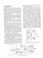
1
nual
$eftice
six-3s|oo
FM €Iuartz Locked
S T E R E OR E C E I V E R
()proNEER'
C O M E SI N T W O V E R S I O N SD I S T I N G U I S H E DA S F O L L O W S :
MODELSX.3gOO
Remarks
Voltage
Type
KU
120Vonly
U . S . A .m o d e l
5/U
I 10V, 120V, 22Oand240V (Switchable)
U . S .M i l i t a r y m o d e l
This servicemanual is applicableto the KU type. When repairingthe S/G type, pleaseseethe
additional servicemanual (seepages47 -56l..
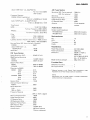
1. SPECIFICATIONS
CONTENTS
1. spECtFtcATtoNS
2
2 ' F R o NPr A N EFLA C I L T T I E S
DIAGRAM
3' BLocK
4 . c l R C UD
lrESCRIPTIoNS
a
7
P o w e rA m p l i f i e rS e c t i o n
C o n t i n u oPuosw e0r u t p u0t f 1 2 0w a t t s x p cehr a n n e l ,m i n . a
, t 8 o h m sf r o m 2 0 H e r t tzo 2 0 , 0 0 0
H e r t zw i t h n 0 m . r e t h a n0 . 0 0 5 %t o l a lh a r m o -
4 . 1 F MT u n eSr e c t i o n
4.2 AM TunerSection
8
9
n i Cd i S t O f t i O n .
4.3
9
g ohms)
c o n t i n u o u s r a t e d p o w e r o u t p u tN. .o m o r e t h a n 0 . 0 0 5 %
6 0 w a t t s p e r c h a n n e lp o w e r
Audio Section
4.4
DisplayCircuits
4.5
P r o t e c t i o nC i r c u i t
current
suppressor
4'6 Surge
.......
11
13
" " " ' l5
15
5 ' D I S A S S E M B L Y' '
1 E
6 . P A R T SL O C A T I O N
16
7 . D I A L C O R DS T R I N G I N G.
g. ADJUSTMENTS
18
Section
8.1 Audio
8.2
T u n e rS e c t i o n .
1e
(20Hertzto 20,000
Hertz,
Distortion
To,rlHarmonic
,",1r',jlltr,r.ion
oirioriion
iuorrrrrltrl;f ;::ltjT:"fl
c o n t i n u o ursa t e dp o w e ro u t p u t . . N o m o r et h a n0 . 0 0 5 %
6 0 w a t t sp e rc h a n n epl o w e r
' . . . ' N o m o r et h a n0 . 0 0 5 %
output
R
e
s
p
o
n
s
e
Frequency
*! aa
T iorTln?,t'.2
rnpr.s.nriiiui,vli,.np.oun..t,i;ff
20
DIAGRAM
9, SCHEMATIC
p
.
c
.
B o A R D Sc o N N E C T T o ND T A G R A M
10.
24
I1.PARTSLIST.
35
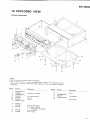
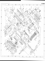
1 2 . E X p L o D E Dv t E W
41
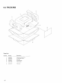
1 3 .P A C K | N G . . . .
46
E A N U A L F O RS / GT Y P E
A D D T T T O N ASLE R V T CM
41
29
.....
'l
V/50kilohms
OUtPUt
' ' ' ' ' A' B' A+B
-speaker
D a m p i n gF a c t o r( 2 0 H e r t zt o 2 0 , 0 0 0H e r t z ,8 o h m s )
...60
r t r . i r .i i H i , r r r o r t c i r c u i t eAo ,n e t w o r k )
Hr..;;
115d8
""'
P r e a m p l i f i e rS e c t i o n
In p u t ( S e n s i t i v i t y / l m p e d a n c e )
2 . 5 m V / 5 0k i l o h m s
P H O N O1 , 2 . . .
A U X , T A P EP L A Y 1 , 2 ,
... 150mV/50kilohms
...
ADAPTORIN
P h o n oO v e r l o a dL e v e l( T . H . D .0 . 0 0 5 %1, , 0 0 0H e r t z )
300mV
PHONO
1.2...
l Pedance)
O u t P u t( L e v e l /m
T A P ER E C1 , 2 . A D A P T O RO U T
150mV
PREAMP
O U T ( R L :5 0 k i l o h m s )
. . . . 1 V l 1 k i l o h m s( V o l u m e :m a x . )
T o t a l H a r m o n i cD i s t o r t i o n( 2 0 H e r t zt o 2 0 . 0 0 0H e r t z )
P H O N O1 . 2 ( R E CO U T ) . . . . . . N o m o r et h a n0 . 0 0 5 %
( 1 0 Vo u t p u t )
sx-3900
A U X , T A P EP L A Y 1 , 2 . A D A P T O RI N
No more than 0.005%
(10V output)
F r e q u e n cR
y esponse
P H O N O( RI A A E q u a l i z a t i o n )
. . . 2 0 H e r t zt o 2 0 , 0 0 0H e r t zt 0 . 2 d B
A U X , T A P EP L A Y 1 , 2 ,A D A P T O R
OUT
+9
' ' ' ' ' 7 H e r t zt o 8 0 0 0 0 H e r t z d B
Ton. contror
B A S S.
TREBLE
AM TunerSection
S e n s i t i v i t (yl H F , F e r r i t ea n t e n n a .) . 300sV/m
(lHF, Ext. antenna)" .
1SpV
Selectivity
30dB
S i g n a l - t o - N o i sR
e atio
50dB
l m a g e R e s p o n s eR a t i o
40dB
l F R e s p o n sR
e atio. .
40dB
Antenna
F e r r i t el o o p s t i c k
an t e n n a
! 4 d B / ! 7 d B( 1 0 0 H 2 )
f u rnoverFrequency
: 2OOHz/
400H2
(10kHz)
+gdB/t7dB
Tu rnoverFrequencv
: 2kHzI 4k{z
Filter
L O W ..
1 5 H z( - 6 d B / o c t . )
HIGH.
8 k H z( - 6 d B / o c t . )
L o u d n e sC
s o n t o u r( V o l u m ec o n t r o ls e t a t - 4 0 d B p o s i t i o n )
. . . . + 6 d B( 1 0 0 H 2 )+, 3 d B( 1 00 0 0 H 2 )
H u m a n dN o i s e( l HF , s h o r t - c i r c u i t e
Adn, e t w o r k )
PHONO
. .. . .. 86dB
A U X , T A P EP L A Y 1 , 2 ,
ADAPTORIN...
10 5 d B
-20d8
Attenuator.
FM Tuner Section
U s a b lS
e e n s i t i v i t( yl HF)
5 0 d BO u i e t i n gS e n s i t i v i t y
MONO
STEREO
S i g n a l - t o - N o iR
s ea t i o
MONO
S T ERE O
D i s t o r t i o n( a t 6 5 d B f)
MONO 100H2.
lkHz .
6kHz '
S T E R E O1 0 0 H 2 .
ikHz .
6kHz
O u t p u t( L e v e l /m
l pedance)
F M ( 1 0 0 %M o d . ) .
A M ( 3 0 %M o d . ) .
6 5 0 m V / 2 . 4k i l o h m s
20OmV/2.4 kilohms
Semiconductors
lCs...
FETs.
T r an s i s t o r s
Diodes
M iscellaneous
P o w e rR e q u i r e m e n t s
P o w e rC o n s u m p t i o n
Dimensions
9 . 8 d B f( 1 . 7 p V )
t5
o
89
62
AC 120V.60H2
3 5 0 W( U L )
5 2 6 ( W x) 1 7 6 ( H )x
4 5 2 ( D )m m
2 0 - 1 1 / 1 6 ( wxl 6 - 15 / 1 6
( H ) x 1 7 - 1 4 / 1 6 ( Di nl
2Okg(441b 2ozl
14.2dBf(2.8pV)
3 6 d B f( 3 4 . 7 p V )
Weight(without package)
8 3 d B( a t 6 5 d B f )
7 8 d B( a t 8 0 d B f )
O p e r a t i n gi n s t r u c t i o n s
FM T-type antenna
0.1o/o
* Measured pursuant to
the Federal Trade Commission's
Regulation rule on Power Output Claims for Amplifiers.
FurnishedParts
o.o7%
oJ%
O.27o
o.15%
O.2To
C a p t u r eR a t i o . .
1.0d8
A l t e r n a t e C h a n n e lS e l e c t i v i t y
400kHz
......80dB
S t e r e oS e p a r a t i o n
1 k H z .
. . . . . . 5 0 d 8
3OHzto15kllz.
......
35dB
F r e q u e n c yR e s p o n s e
....2OHzto15kHz1!jaa
Spurious
Response
Ratio. . . . . . . 100dB
lmageResponseRatio
...
lFResponseRatio..
....
AMSuppressionRatio
...
S u b c a r r i e r P r o d u c tR a t i o . . . . . . .
SCARejectionRatio
....
M u t i n gT h r e s h o l d
Antenna Input .
Audio Section
90dB
100d8
60dB
64dB
64dB
1 9 . 2 d B f( S g V )
300 ohms balanced,
75 ohms unbalanced.
1
1
Trade
NOTE:
Specifications and the design subject to possible modifications
without notice due to improvements.
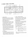
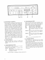
2 . F R O N T P A N E LF A C I L I T I E S
O POWERSWITCH
SWITCH
O T R E B L ET U R N O V E R
SetthisswitchtooNtosupp|ypowertothereceiver.
is setto ON' because
Therewill be a shortdelaywhen it
the
to suppress
the muting circuit has been actuated
the
when
generated
unpleasantnoisethat is sometimes
off '
Poweris switchedon and
@ BASSTURNOVERSWITCH
frequency in which
Use this switch to change over the
bass control is starting
the sound adlustment with the
or 400H2 in accordance
to take effect. Select 200H2
withthecharacterlstics'ofyourIisteningroomandof
preference'
y o u r s p e a k e r sa, n d w i t h y o u r g e n e r a l
@ E A S SA N D T R E B L EC O N T R O L S
bass and the treble'
Use these controls to adiust the
and turn the bass
ON
lf you set the tone switch to
controItotherightfromitscenterposition,youwi||be
ab|etoemphasizethesoundinafrequencyrangewhich
bassturnover switch'
is lower than that selectedby the
f
r
o
m t h e c e n t e rp o s i t i o n
c
o
n
t
r
o
l
C o n v e r s e l y t, u r n i n g t h i s
to the left will attenuate the sound'
adjust the sound in a
You can use the treble control to
by the treble turnfrequency higher than that selected
over switch.
@ T O N ES W I T C H
bassand treble
Set this switch to ON when adjustingthe
tone control
c o n t r o l s .W h e n s e t t o t h e O F F p o s i t i o n 't h e
circuitsaredisengagedandfrequencyresponseisf|at.
Thisfunctionisconvenientforcheckingphonocartridge
room acoustics'
a n d s p e a k e rt o n e q u a l i t y a n d l i s t e n i n g
the frequency in which
Use this switch to change over
treble control is starting
the sound adjustment with the
or 4kHz in accordance
to take effect' Select 2k{z
withthecharacteristicsofyourIisteningroomandof
preference'
y o u r s p e a k e r sa, n d w i t h y o u r g e n e r a l
@ noRProRswlrcH
SetthisswitchtooNwhenreproducingsoundfroman
to the ADAPoptional componentwhich is connected
p
o
s
i t i o ni f y o u a r e
upper
T O R i a c k sA
. l w a y ss e ti t t o t h e
n o t u s i n ga c o m p o n e nwt i t h t h e s et e r m i n a l s '
SWITCH
@ T A P ED U P L I C A T E
you want to duplicate or
Set this switch to ON when
two tape decks'
edit a pre-recorded tape using
@ T A P EM O N I T O RS W I T C H
a r e c o r d i n gi n
E m p l o y f o r t a p e p l a y b a c ko r t o m o n i t o r
progress.
P l a y b a c ko r m o n i t o r i n g o f a t a p e d e c k c o n 1:
nected to the TAPE 1 jacks'
position when not
SOURCE: Be sure to set to this
monip
usingthe tape deck for laybackand
2:
tori ng'
conP l a y b a c ko r m o n i t o r i n g o f a t a p e d e c k
jacks'
nected to the TAPE 2
NOTE:
be sure to set this
When listeningto recordsor broadcasts'
from speakers
obtained
be
not
witt
switch to SOURCE' Sound
if it is setto 1 or 2.
six-39cl(f
€) BALANCECONTROL
U s e t h i s c o n t r o l t o b a l a n c et h e v o l u m e o f t h e l e f t a n d
r i g h t c h a n n e l s .F i r s t , h o w e v e r , s e t t h e m o d e s w i t c h t o
M O N O . l f t h e s o u n d a p p e a r st o b e l o u d e r o n t h e r i g h t , i t
means that the volume of the right channel is higher.
Turn the balancecontrol to the left and adjust.Conv e r s e l y ,i f t h e s o u n d a p p e a r st o b e l o u d e r o n t h e l e f t , i t
meansthat the volume of the left channel is higher.
T h e r e f o r e . t u r n t h e b a l a n c ec o n t r o l t o t h e r i g h t a n d
a dj u s t . A f t e r a d j u s t i n g , r e t u r n t h e m o d e s w i t c h t o
STEREO.
@ M O D ES W T T C H
U s e t h i s s w i t c h f o r s e l e c t i n gm o n o o r s t e r e o p e r f o r m a nces.
STEREO: Set to this position for normal operations.
MONO:
W h e n s e t t o t h i s p o s i t i o n ,t h e l e f t a n d r i g h t
c h a n n e l s i g n a l sw i l l b e m i x e d a n d r e p r o duced monophonically from both speaker
systems.
o v o L U M EC O N T R O L
Use this control to adjust the output level to the
s p e a k e r sa n d h e a d p h o n e sT. u r n i t c l o c k w l s et o i n c r e a s e
t h e o u t p u t l e v e l .N o s o u n d w i l l b e h e a r d i f y o u s e t i t t o
-. The scale is graduated in dB which indicate the
a t t e n u a t i o nw h e n t h e m a x i m u m o u t p u t l e v e li s 0 d B .
€ ) M U T I N GS W I T C H
Set this switch to the *20d8 position to attenuate the
a u d i o o u t p u t i n d i c a t e db y t h e v o l u m e c o n t r o l b y 2 0 d B .
T h e r e i s n o n e e d t o a d j u s tt h e v o l u m e c o n t r o l i f y o u u s e
this switch when turning down the audio output temp o r a r i l y a n d w h e n c h a n g i n go v e r r e c o r d so r t a p e s .
G ) H E A D P H O NJEA C K
P l u g t h e h e a d p h o n e si n t o t h i s j a c k w h e n y o u w a n t t o
l i s t e nt h r o u g h y o u r s t e r e oh e a d p h o n e s .
Releaseboth speaker switches if you want to listen to
t h e s o u n d t h r o u g h y o u r h e a d p h o n e so n l y .
(E SPEAKER
SWITCHES
D e p r e s st h e s w i t c h c o r r e s p o n d i n gt o t h e s p e a k e r sc o n n e c t e d t o t h e S P E A K E R St e r m i n a l s( A o r B ) o n t h e r e a r
panel.
You can depress both of these buttons to listen to the
sound from two pairs of speaker systems at the same
time.
(15H2)
@ L O WF I L T E RS W I T C H
D e p r e s st h i s s w i t c h i n t h e e v e n t t h a t t u r n t a b l e r u m b l e ,
recordingcutting noise or other low frequency noise
b e c o m e s o b j e c t i o n a b l e .A t t e n u a t i o n i n t h e f r e q u e n c y
bandbelow 15Hz is6dB/octave.
(8kHz)
G ) H I G H F I L T E RS W I T C H
D e p r e s st h i s s w i t c h i f r e c o r d s c r a t c hn o i s e o r o t h e r h i g h
f r e q u e n c y n o i s e b e c o m e so b j e c t i o n a b l e A
. ttenuation in
t h e f r e q u e n c yb a n d a b o v eS k H z i s 6 d B / o c t a v e .
€ ) P O W E RM E T E R
This meter allows you to read out the rated power level
o n t h e f l u o r e s c e n t d i s p l a y t u b e w h e n s p e a k e r sw i t h a
nominal impedanceof 8 ohms are connected to the
s p e a k e rt e r m i n a l s .
@ DrALPOTNTER
T h i s p o i n t e r i n d i c a t e st h e b r o a d c a s t i n gs t a t i o n s .
rNDrcAToR
@ rnnSTEREo
T h i s i n d i c a t o rl i g h t s u p w h e n r e c e i v i n ga n F M s t e r e o
p r o g r a mi f t h e F M m u t i n go f f s w i t c hi s r e l e a s e d .
@ o U A R T Z L O C K E D| N D | C A T O R
This indicatorlightsup after the optimum tuning point
h a s b e e n o b t a i n e d a n d d i s p l a y st h a t t h e r e c e i v i n gs t a t e i s
s t a b i l i z e db y t h e b u i l t - i n q u a r t z l o c k c i r c u i t .
€D SIGNAL INDICATOR
T h i s i n d i c a t o r l i g h t s i n s e q u e n c ef r o m l e f t t h r o u g h r i g h t
d u r i n g t h e t u n i n g o f a n A M o r F M b r o a d c a s ti n a c c o r d a n c e w i t h t h e s t r e n g t h o f t h e s i g n a l sb e i n g r e c e i v e d .
The optimum tuning point is where the maximum
n u m b e r o f i n d i c a t o r sl i g h t .
rNDrcAToR
@ rururNG
W h e n t u n i n g i n a n F M s t a t i o n ,t h e o p t i m u m r e c e p t i o n
p o i n t i s i n d i c a t e dw h e n t h e c e n t e r i n d i c a t o r l i g h t s u p .
W h e n t h e l e f t i n d i c a t o rh a s c o m e o n , r o t a t e t h e t u n i n g
k n o b s l i g h t l y c l o c k w i s e .W h e n t h e r i g h t i n d i c a t o rc o m e s
o n , r o t a t e t h e k n o b s l i g h t l yc o u n t e r - c l o c k w i s e .
YI S P L A Y
@ F R E O U E N CD
T h i s i n d i c a t e st h e f r e q u e n c yw h i c h i s t u n e d .
W i t h F M r e c e p t i o n ,t h e l e t t e r s " F M " a p p e a ro n t h e l e f t
of the displayand "MHz" on the right. With AM recept i o n , " A M " a p p e a r so n t h e l e f t a n d " k H z " o n t h e r i g h t .
These change when the function selectorposition is
c h an g e d .
@ T U N I N GK N O B
U s et h i s k n o b t o t u n e i n t o b r o a d c a s t i n gs t a t i o n s .
5
@ F M M U T I N GO F F S W I T C H
tuned
W h e n t h i s s w i t c h i s r e l e a s e da n d a n F M b r o a d c a s
s
u
p
p
r
e
s st h e
t
o
i
n
s
i
d
e
in, the muting circuit is activated
broadcasting
the
between
annoying interstation noise
' henthe broadcastf r e q u e n c i e sf o r n o i s e - f r e er e c e p t i o n W
r
e
c
e i v i n ga s t a t i o n i n a
w
h
e
n
ing station is far away or
O
F
F p o s i t i o na n d t h e n
t
h
e
t
o
f r i n g e a r e a ,s e t t n e s w i t c h
with a strong
station
tune in. lf there is a broadcasting
program
whose
station
a
to
signal level on the air next
tune in
to
able
be
not
you
may
you want to receive,
d
r
o
w
n
ed out
b
e
w
i
l
l
s
o
u
n
d
t
h
e
s a t i s f a c t o r i l yb e c a u s e
t
h
e FM
s
e
t
t
h
i
s
'
l
i
k
e
c
a
s
e
s
I
n
by the stronger signals'
p
o
s
i
t
i
o
n
)and
(
d
e
p
r
e
s
s
e
d
O
F
F
MUTING OFF switch to
the
w
h
e
n
w
o
r
k
n
o
t
d
o
e
s
tune in. The muting circuit
b
e
en
h
a
s
t
u
n
i
n
g
l
f
b
r
o
a
d
c
a
s
t
s
'
t u n e r i s r e c e i v i n gA M
b
e
en
h
a
s
s
w
i
t
c
h
O
F
F
M
U
T
I
N
G
F
M
p e r f o r m e da f t e r t h e
quartz
locked
the
selected.
depressed and a station
the LOCKED
circuit is set to the OFF mode and
i n d i c a t o rd o e s n o t l i g h t .
@ FM 25PSSWITCH
a Dolby* FM
Depressthis switch when listening to
the released
at
switch
broadcast; otherwise keep this
position.
@ ) B R I G H T N E SSSE L E C T O R
of the power
Use this switch to select the brightness
m e t e r a n d t h e f r e q u e n c Yd i s P l a Y '
or other
B R I G H T : W h e n u s i n g t h e r e c e i v e ri n d a y l i g h t
DIM:
SELECTOR
@ FUNCTION
to the
Deoress the function switch which corresponds
first
d
o
w
n
program source.Turn the volume control
the
w
h
i
l
e
b e f o r e s e l e c t i n ga d i f f e r e n t f u n c t i o n s w i t c h
s o u n d f r o m o n e p r o g r a ms o u r c ei s b e i n g r e p r o d u c e d '
FM:
AM:
AUX:
this switchfor FM broadcasts'
Depress
this switchfor AM broadcasts
Deoress
an
D e p r e s st h i s s w i t c h w h e n l i s t e n i n g t o
AUX
the
to
audio component connected
iacks.
p l a y i n ga r e c o r d o n
P H O N O 2 : D e p r e s st h i s s w i t c h w h e n
the turntable connectedto the PHONO 2
j a ck s .
p l a y i n ga r e c o r d o n
P H O N O 1 : D e p r e s st h i s s w i t c h w h e n
1
the turntable connected to the PHONO
iacks.
NOTE:
a ilme'
OnlY one function switch should be depressedat
@ L O U D N E SS W l r c H
the volume
When listening to a performance with
and the bass
control turned down, depressthis switch
a n d t r e b l ew i l l b e a c c e n t u a t e d '
i t h a r d e rt o
f
Whenthe volumeis low, the human ear inds
volume is high'
h e a r t h e b a s sa n d t r e b l e t h a n w h e n t h e
for
The loudnessswitch is thus designedto compensate
a
nd
b
a
s
s
t
h
e
t h i s d e fi c i e n c y . B y d e p r e s s i n gt h i s s w i t c h '
s
o
u
nd
t
h
e
a
n
d
treble come through much more strongly
is
c
o
n
t
r
o
l
takes on a puncn even when the volume
turneddown.
bright locations'
A t n i g h t o r i n d a r k l o c a t i o n sw h e n t h e e x i s t i n g b r i g h t n e s si s t o o h i g h '
*Theword,,Dolby''isatrademarkofDoIbyLaboratoriesInc.
sx-39clcl
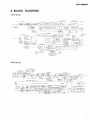
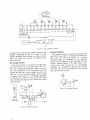
3. BLOCK DIAGRAM
Tuner Section
r c ( H A l 2 0 1 )0
OUARIZ LOCKEO
AM TUNER
5-POINT SIGNAL
I N D I C A T O RO R I V E
A M O
rUN]NG INDICATOR
FREOUINCY
FM
OISPLAY
MHz
,ODDD
, t_, t_t.t_t t_t
AM
CoUNTER
Oi - D5
TIME DIVISION
7- SE6M€NT OECOD€R
ROM
s1s2 s3 s4
Audio Section
IAPE 1 _-. ^
REC PLAY
.":-
ADAPrcR
OUT IN
ar lr
R CnANNE- . IHL SAME A5
IHF
L CHAN\EL )
FREA!ENCY
FL TUSE
'UIER
SECTION
KHT
apIF system IC (PA300?-A), it is amplified and
conwhich
4-1)
Fig'
(see
detector
to a crystal
a series
sists of diodes connected in parallel in
resonacrystal
a
with
equipped
circuit
resonance
as
the IF
same
the
is
frequency
i.r. irt" resonance
fr"qr".r"y (10'?MHz), which meansthe impedance
in the outat it ls time will be minimal, resulting
level' If the input
fut being reduced to a minimum
capaciiruq.r"rr"y increases-the reactance of the
of the
tanie stage(C) is reduced,and the reactance
AM
in
ir"rar"tun"u stage (L) increased,resulting
portion
positive
Jetection by D2 which leavesthe
decreases'
frequency
input
If
the
IF
signal.
of the
reacC
stage
and
decreased
is
reactance
L stage
D1
by
tance increased,resulting in AM detection
IF
signal'
which leavesthe negativeportion of the
as the
it'r" t stageand C stagereactancesinctease
is
degree oidetuning in the respectivedirections
in
in&eased, resulting in a subsequentincrease
S-curve
the detector output. By thus attaining
possible'
characteristics,FM detection becomes
deviaSince the IF signalis an FM signalfrequency
be
symmetrical
tiorl-a"" to iodulation, it will
is
about a central axis. And if the central frequency
outdetector
the
equal to the resonancefrequency,
o,rt OC level will be zero. If, however,there is any
displacement in the central frequency, frequency
become
deviation in respect to the detector will
a DC
of
generation
aryrrr-utri"a1, resulting in the
LPF1
through
passed
This DC voitage is
"liiug".
(IF filter) and LPF2 (AC filter) to form a correccapaciiion voltage which is applied to the variable
tancediodeinthelocaloscillator,therebycorrectconstant
ing the oscillator frequency to obtain a
frequency)'
tn' (i.e. a constanttuned
detecSince the central frequency of the crystal
tuned
resonator'
crystal
the
tor is regulated by
obare
stability
high
frequencies of exiremely
tained.
4 . C I R C U I TD E S C R I P T I O N Sptiei
4 . 1 F M T U N E RS E C T I O N
Front End
a 4
The FM front end of SX-3900 includes
FETMOS
ganged tuning capacitor, a dual-gate
a modified
Eo"Too"A l-slage RF amplifier' and
is a
oscillator
This
circuit llcal oscillator'
ai;;
vari-cap
a
uoiiug" controled oscillator employing
(varia'blecapacitancediode)' When the.quartz-lock
is not in
,yrt"..t (refer to "Quartz-lock system")
to the
applied
is
operution, a constant voltage
diode.
lF Amplifier and Detector
Theseemploy 3 ICs and 3 dual-elementceramic
stageconfilters. fne lC (HA1201) of the first 2
currentamplifier
stitutes a single-stagedifferential
third
the
(PA300?-A)-in
ii-lti.rg limitet. The IC
IC
iF
system
former
stage,an improvement on the
amplifier'
iimiter
iF
ai, includes an
liigool
cirquadrature detector, meter drive' and other
S/N
distortion'
of
cuits. Performance in terms
parameters'
ratio, delay characteristics,and other
to
comparison
in
,ho*, a marked improvement
the PA3001-A.
Ouartz-LockSYstem
SX-3900
The quartz-lock systemfeaturedin the
system
control
serl/o
stereo receiver is a frequency
displacement
Any
employing a crystal resonator'
detected as a
i.r itt"-lntlrmediate frequency (IF) is
with a
(equipped
DC voltage by the discriminator
oscillator
local
the
in
crystal resonator)' resulting
ir"qt"r-r"y being corrected and subsequently
servoconlocked. This extremely stablefrequency
frequencies
tuned
that
trol system thus ensures
remain tuned securelyfor aslong asrequired'
of the
When the IF signalappearsat pin no'17
l c ( P A5 0 0 7 - A )
F M F R O N TE N D
CRYSTAL DETECTOR
|
: ( L )
C I R C UI T
F i g .4 - 1 O u a r t zL o c kS Y s t e m
a
----,
1 3
+ i
I
sx-39clo
o Limiting the Locking Range
If the quartzJock range is too wide, it will
overlap with strong adjacent broadcasting frequencies and result in considerable tuning difficulties. A DC amplifier is therefore used as a
limiter (limiter action by NFB circuit zener diodes)
which restricts the voltage applied to the variable
capacitance diode, thereby limiting the quartz-lock
range.
A DC voltage appears at pin no.13 of the IF
system IC (PA3007-A) when the antenna input
ievel drops below 5pV, or when the tuned frequency has been detuned by more than t100kHz.
This DC voltage (FM muting signal) is applied to
the gate of Q2 (FET) via a Schmitt circuit, resulting in the FET being turned on, and the quartzIock circuit being turned off.
Multiplex Decoder
The recently developed multiplex decoder IC
(PA4006-A) combines MPX decoding with muting
functions in a single IC, thereby handling the
functions of the more conventional MPX IC
(PA1001 A) and AF MUTING IC (PA1002-A).
Distortion ratings and S/N ratio have been
further improved by incorporating a chopper type
MPX decoder. The chopper type switching circuit
(see Fig. 4-2) operates by switching the signal
either to ground or to the through circuit, thereby
eliminating the generation of unwanted noise or
distortion. Furthermore, since the PA4006--4 features DC direct-coupled switching with the detector, there is no deterioration in separation at the
Iow frequency end.
Besides the decoder and muting circuits, the
PA4006-.4 also incorporates the pilot signal canceller, stereo auto selector, VCO killer circuit, MU'l
amplifier. and MUT control circuit.
Composite
si g n a l
Inprt
4 . 3 A U D I OS E C T I O N
P h o n oE q u a l i z eArm p l i fi e r
Fig. 4-3 shows the basic configuration of the
circuit. An S-N ratio of 86dB (at 2.5mV input,
IHF-A) has been achieved by using a ultra-lownoise PNP transistor (2SA978) at the first stage,
and reducing the signal source resistance and
equalizer element impedance. High voltage gain is
provided in the following stage by a bootstrap circuit. The output stage is a complementary symmetrical SEPP circuit. The high voltage utility
factor of the SEPP circuit provides a high maximum output
voltage. Dynamic
range of the
equalizer amplifier is therefore wide and overload
input level at 0.005% distortion is 300mV (rms at
lkHz).
tNHMrl
F i g .4 - 3 P h o n o E q u a l i z e A
r m p l i fi e r
Tone Control
Fig. 4-4 shows the basic configuration of the
circuit. This circuit is an NFB type tone control
with IC (HA12017P).
Tone control (BASS, TREBLE) is accomplished
by providing the tone amplifier NFB circuit with
a frequency selective characteristic. The capacitance of C7-C4 are changedby the TURNOVER
switches (by adding another capacitors in parallel)
to provide selectionof the frequency.
The NFB circuit is changedto a flat frequency
characteristicwhen the TONE switch in the OFF
oosition.
Output
JUIIUUUIJUIJU'.}. --'II
,in"r'r
switchins
S/
n
L
F i g . 4 - 2 C h o p p e rT y p e S w i t c h i n gC i r c u i t
4 . 2 A M T U N E RS E C T I O N
The AM tuner section consists of a 2-ganged
tuning capacitor plus an IC (HA1197) which contains a 1-stage RF amplifier, converter, 2-stage IF
amplifier, detector, and AGC circuit.
The AM STEREO OUT terminal on the rear
panel is for connecting to an AM stereo broadcast
decoder adaptor. The signal appearing at this terminal is the converter output passed via a buffer
(emitter-follower) stage.
Tone Control
junctions formed by
bias circuit consisting of 4 PN
Power AmPlif ier Section
VR1'
D3 and Q4, and
Q3,
--Witft
flow of
o Amplifier Circuit
R1 and D1 ensuring a constart
be
power
may
X
the
of
point
and
The basic circuit arrangement
current, the base of Q1
(level
a
is
stage
basis
AC
The
an
4-5'
on
Fig'
level
it shown in
-first
brought to the same
"-pilii"t
amplifier comprising PNP twin transisfluctuationsduetothesignal)byasimpleshiftin
aiti*""ti"f
is a current
be considered
i.t te2l, the load circuit of which
DC level. Furthermore, Q1 may
(QB)'
transistor
resistance'
twin
emitter
NPN
the
an
as
with R3
employing
;*;;
X is inY
and
points
"-iti"t-toffower
Thecurrentmirrorprovidespush-pulloperationin
When the voltage across
harmonics
apsignal
even
th.e
cancel
of
to
portion
serves
this stage, which
creased by the positive
signal
input
the
gain'
becomel.
it
itrls cirluit,
and
-- further increase
;i*i-;"
outflow of base
(Q1). since the emitteremitter_follower
Qf in the input &cuit absorbs
it-trri,
of a
generation
the
prevents
and
current from Q2,
followervoltagegainispracticallyl,avoltage
temperature
DC voltage. BecauseQ1 follows any
m o r e o r l e s s e q u a l t o t h a t o f t h e i n pY
utsignal
the center point
increaseacrosspoints and X)
voltage
drift in Q2, temperature drift of
the
it,
iirr"i
is the voltat R5. And the R3 voltage
voltage is Prevented.
ir^*"J"""a
Darlington
of Q3
a
is.
(Q4,
collector
and
Q5)
stage
base
The pre-driver
age applied across the
a
employs
circuit'
which
of
circuit
power
load
jt"g:
the
the
**g"-".rt,
Pi"tin excess
which forms part of
be
bias voltage applied to Q3 will
constant-currentsource(Q6)resultingahighvoltil;h"
points Y
across
voltage
ttt"
gain.
age
by the same amou"i
"
the
by
portion. of the signal)
Tite power stagebias voltage is supplied
and X increased(by positive
high
The
circuit'
no signal is being
when
sewocontrol
level
high spe"a bias
above the voltage
nonprovides
speea bias servocontrol circuit
applied. Consequently, the increase 1" l:]1"?:rn
(refer to
stage
power
cancels the decrease
the
in
,^*it"t ing operation
lii"t.
o.i"ts Y and X
Z't}r,ereby maintaining
;'High SpeeaBias Servocontrol Circuit")'
and
X
points
toii"g"'u"t"ss
Darlingthe PNP power
a.2-stage
is
cutiing
(Q7
without
Q12)
The power stage
the idle current
SEPP
parallel
is
ton arrangement, tite tinat stage
constant in the
time
no
is
there
circuit. Bicause
amplifiNFB circuit in the low frequency region'
inputs will be
cation is possible down to DC (DC
however, by the input coupling capacitor)'
""l.it,
o High Speed Bias Servocontrol Circuit
within the
By operating the power stage.only
with miniactive region 1no possible cut-off).and
servocontrol
bias
mum idle current,'the high speed
discircuit prevents the generation of switching
tortion and reducesheat loss'
When there
This circuit is outlined in Fig' 4-6'
circuit'
Q1 and Q2 are
is no signal applied to the
be on' The
will
and
Q4
almost iut off' while Q3
of both of
base
and
uoitug" across the collector
RI V
P R E -O
"e
aEsRi "
may be
time
this
at
C l r c , i t r vo f N o n - s w i t c h i nAgm p l i f i e r
t'n. d-d
these transistors (Q3 and Q4)
stage
power
the
with
disregarded. Consequently,
*l
||'.l
I
nl
Fi s . 4 - 5 P o w e r A m P l i f i e r C i r c u i t
sx-39ocl
stage off (noting that there actually is a slight decrease in current). For the negative portions of the
signal, Q2 and Q4 are operated in the same manner, thereby preventing the NPN power stage from
being cut off.
4.4 DISPLAY CIRCUIT
Power lndicator Circuit
The SX-3900 output power indicators feature
fluorescent indicator tube (FL tube). In this tube,
thermionic emissions from the cathode are accelerated into the fluorescent substance of the
segmental anodes, resulting in the emission of light.
This tube is used to indicate numerals, letters and
other symbols.
An outline of the FL tube drive circuit is shown
in Fig. 4-7 .'lhe output circuit signal is first passed
through a low-pass filter and a compressor circuit
before being applied to pin no.6 (4) of the IC
(TA7318P-A). The compressor circuit makes use
of the non-linearity of rising portion of the diode's
Vd-Id characteristics to contract the signal dynamic range by 20dB. The IC contains a detector circuit, compressor (40dB), and peak hold circuit for
both left and right channels. The dynamic range
of the signal is thus contracted by 6OdB to obtairr
a "peak held" DC voltage.
The output power indicator segments of the FL
tube are driven by the HA12010 ICs (one for each
channel) equipped with 12 pairs of voltage comparators. These comparators are biased at increasing levels, so each comparator will commence to
operate separately as the input level increases.
And since these comparators apply the voltages to
the output power indicator segments, each successive segment will light up in tum as the input level
rises.
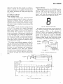
FrequencyDisplay
Frequenciesreceived by the SX-3900 are displayed in digital form by fluorescent indicator
tube (FL tube). Each digit employs up to 7 segments (a - g) (see Fig. 4-8) to display all numerals
from 0 to 9 (with the exception of the left hand
digit which employs only 2 segmentsb and c).
o
F
F i g . 4 - 8 7 - S e g m eD
n ti g i tD i s p l a y
The signal source during both AM and FM reception is the local oscillator. The signal is passedvia a
buffer
amplifier (FET) to the prescalar IC
(M54451P) where it is subjected to frequency division (1/8 for AM and 1/80 for FM) before being
applied to the frequency counter IC (PD5009).
This IC is responsible for the dynamic drive of the
7-segment 5-digit display (each digit being tumed
on according to time-shared sequential scanning).
rc (M54451P)
FM LOCAL
O S C , SI GN A L
FM-AM SELECTION
SIGNAL
tc (fA7318P-At
1/2
LPF
' | N + +
m
t c ( H A i 2 o r o)
I
fltl
E-
-fl
I
w(8rl )
o.oo1
--
--
tr n Dtr !!
!I
t
EE tr n Dt]
l
O.O1
O.1
FL TUBE
F i g . 4 - 9 F r e q u e n c yD i s p l a yC i r c u i t
5;6141+O---1-t!rr-f{
t
7r7
rc(P05009)
AM LOCAL
O S C , SI G NA L
1
FL TUEE
F i g . 4 - 7 P o w e r I n d i c a t o rC i r c u i t
l
10
pO
D5
B R I G H TN E S S
SELECTION
D4
03
DIGIT DRIVER
MULTIPLEXER
c o N T R O LC I R C U I T L A T C H
LOAD
GATE
PRESETAALE 5'DIGI'T
DECIMAL COUNTER
D E C IM A L
COUNTER
FROM -P R E S C A LA R
22-BlT
Vcc
x 16
ROM
GNO
o f C o u n t elrC ( P D 5 0 0 9 )
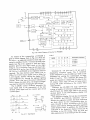
F i o . 4 - 1 0 B l o c kD i a g r a m
PD5009 is
An outline of the composition of
the
given in block diagram form in Fig' 4-10' With
condigit
FL tube a - g segments(anode) for each
pulse
nected in parallel, the D1 D5 time division
(indegrid
;i;"dr (rel nig. 4-11) applied to each
grid ior each digit) result in .the digits
G;J""i
hand side'
being Iit up in successionfrom the left
5ms internacf,"aigit is lit up for 1ms during each
selector
tul. Pin"no.? of PD500g is the brightness
set to
is
width
terminal. The time division pulse
for
200ps
to
and
;00u; for H level input signals,
FL
of
degree
the
L Ievel signals, therety varying
lighting
segment
(by varying the
tube brightness
"Note
that since the power indicator FL
perioa).
of brightiune is driven by static drive, the degree
grid
voltage'
the
,r"rr rrruy be varied by changing
the
ffre f.f ZUHz crystal oscillator generates
time
the
of
preparation
basic signal used in the
gate circuit
aiuirlon.-p.tlse signal and the counter
control signal.
F i g . 4 - 11 D i s i t S i g n a l
Table 1
l n t e r m e d i a t ef r e q u e n c Y
10.67MH2
'10.70MH2
10.73MH2
- 6)^are used in
Terminals S1 54 (pin nos'3
reception mode' The 2 reception
d"i;;;tt";
(seeTable 1) are
;;d"t emptoved in the SX-3900
of input
bv varving
-rri" the combination
;;;;;;J
FM
during
IFs
s different
;;;i; iH uni l;'
the
in
offset
)re required in coping witir ]f
;.;;
preset
being
54
IF ceramic filter stage, 53 and
the ceramic filter
arrring FM mode acc-ordingto
characteristics.
"^'Aftfto.,gft
the SX-3900 FM stage quartz-lock
"capable
of locking any frequency within
.Vrt"- is
(digit in the second
;ir;FM bani, the 10kHz digit
decimalplace)intheFMfrequencydisplaywill
appearonlY as 5 or 0'
.*htu
FL tube-alsoincorporates
^SiCXaL
fr"qrrerr"y display
inclicators' And alttre iUNf-fqC ana
for these indicators
though the segments(anode)
drive cirur" ,iuti" driven uy itre corresponding
D3 time
the
to
tf," grid is driven according
segments
the
placing
",ritr,
pu"lsetiming, thereby
liilit"
the AM and FM
;;J", djnamic a'iul' ttt addition'
i n d i c a t o r s i n t h e l r e q u e n c y d i s p l a y s e c t i o n aand
relit
while the kHz
according to the OS timing'
the D1 timing'
MHz indicatorsare lit accordingto
sx-39ocl
TUNING lndicatorCircuit
The TUNING indicator consists of a center
tuning indicator (which lights up when a broadcasting station frequency is properly tuned) and
2 detuning direction indicators which indicate the
direction in wnich the station has been tuned away
from. The corresponding drive circuits are outlined in Fig.4-72.
The TUNING indicator is activated once the
station has been tuned to within t100kHz of the
center frequency. This is because Q16 is turned
on and Q21 turned off (resulting in the detector
differential amplifier [Q19 & Q20] being turned
off and Q24 being turned on) by the FM muting
signal appearing at pin no.13 of the IF system IC
(PA3007-A) and passed via the Schmitt circuit
(Q17 & Q18) when the station is tuned away by
more than t100kHz.
The DC voltage on pin no.4 of PA3007-A
describes an S curve when tuning to and away from
a particular broadcasting frequency, the voltage on
pin no.2 serving as the reference level. This DC
voltage is amplified by the differential amplifier
(Q19 & Q20) and then applied to a polarity detector switch circuit (Q22 & Q23).
When tuning to a frequency from the high frequency side (or tuning away from the frequency to
a higher frequency), the voltage on pin no.4 will
be higher than that on pin no.2. The Q20 collector
voltage will thus be lowered and the Q19 collector voltage raised, resulting in Q23 being turned
on, and the higher frequency (right hand side)
detuning direction indicator also being turned on.
When, on the other hand, the broadcasting frequency is approached from the low frequency side
(or when tuning away to a lower frequency) the
pin no.4 voltage will be lower, resulting in Q22
being tumed on to light up the lower frequency
(left hand side) detuning direction indicator. Wherl
either Q22 or Q23 is on, the Q24 base voltage will
be high, resulting in Q24 being tumed on and Q25
turned off, which means that the center tuning
indicator will not be lit up.
Once the broadcasting frequency has been tuned
properly, the voltages on pin nos.2 & 4 will be
equal. Consequently, Q22 and Q23 will both be
turned off, which means that neither of the detuning direction indicators will be on in this case.
And since Q24 is turned off because of the decreased base voltage, Q25 will be turned on, and
the center tuning indicator light up. Furthermore,
C77 is charged up via R99, resulting in Q26 being
turned on, thereby lighting up the Quartz Locked
indicator LED.
SCHl,llTT
CI R C U I T
r ircuit
F i g . 4 - 1 2 T u n i n gI n d i c a t o C
S I G N A L I n d i c a t o rC i r c u i t
The SX-3900 SIGNAL indicator consistsof an
FL tube 5-point indicator display.The signalmeter
drive signal obtained from the FM IF system IC
(PA3007-A) and AM tuner IC (HA1197) is first
amplified and then applied to the indicator drive
IC (HA12010). This IC contains12 pairs of voltage
comparators similar to those employed in the
power indicator circuit, 5 of thesepairs being used
to drivethe SIGNAL indicator(Fig. -13).
CIRCUIT
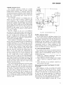
4.5 PROTECTION
purpose
The
of this circuit is to protect both the
speakersand the power amplifiers. The relay in the
output circuit is automatically opened in any of
the following cases:
1. During the "transient operations" when the
power supply is tumed on and off.
2. Upon detection of a DC voltage in the output
circuit, caused by component failure or accident.
3. Upon detection of an overload, causedby a
short circuit in the load.
Muting Operationwhen PowerSupply is Turned
On and Off
With reference to Fig, 4-74 when the power
supply is turned on, Q5 turns off due to -B (The
time constant of the -B circuit is very small.).
If there is no input (DC) on Q3 and Q4, they will
be off, and the timing capacitor C4 charges up
through R8 and R7, and thus Q6 turns on. When
Q6 conducts, the relay operates,and the output
muting on the power amplifier will be removed.
When the power supply is turned off, -B will
l c ( H A 1 2 0 1 )0
F i g .4 - 1 3 S i g n a lI n d i c a t o rC i r c u i t
abruptly decay, and Q5 will conduct owing to the
residui component of +B. As a result, C4 will
rapidly discharge,Q6 will ceaseto conduct, whereupon the relay will become de-energized and
restore muting.
DC Voltage Detector
The output circuit is connected to the Q3 emitter and qa trase via a low-pass filter (R5, C2)'
Any DC voltages appearing the output circuit of
the power amplifier, it will be applied to the Q3
emitter and Q4 base. If the voltage is positive, Q4
turns on. C4 will rapidly discharge'If the voltage
is negative, QB tums on' C4 will rapidly discharge'
As consequence,Q6 will turn off and the relay
will become de-energized,thus causingthe output
circuit to oPen.
OverloadDetection
The overload detector circuit incorporates the
load (RL) in one side of a Wheatstonebridge (see
Fig. 4-15). The base and emitter of a sensing
tra'nsistor (Q2) are connected to the opposite
corners of ttre bridge, so if RL decreases,Q2 will
prebecome forward biased. If RL falls below a
scribed value, Q2 will turn on' C4 will rapidly
discharge. As consequence,Q6 will tum off and
the relay will become de-energized,thus causing
the output circuit to oPen.
F i g . 4 - 1 5 O v e r l o a dD e t e c t o r
F i q . 4 - 1 4 P r o t e c t i o nC i r c u i t
sx-39ocl
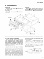
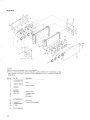
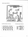
5. DISASSEMBLY
WoodenCover
Remove the two screws (O o.r each side of
the wooden cover.
Bottom Plate
Remove the thirteen screws Q to detach the
bottom plate.
Front Panel
Remove all the knobs by pulling. liemove the
two screws @ from the top edgeof the front panel.
Remove the two nuts @ from the control shafts.
.tt
Front panel
'- \
\--'-=.::att/77
S
\
)rt"
Bottom plate
4 . 6 S U R G EC U R R E N TS U P P R E S S O R
Since the SX-3900 employs a large toroidal
power transformer and two 15,0009F capacitors
in the power supply circuit, the sudden surge of
current when the power supply is turned on may
reach several hundred amperes. The surge current
suppressor circuit used to reduce this sudden
surgeis shown in Fig. 4-16.
When the POWER switch (S1) is OFF (i.e. no
supply of AC power), the relay contact (S2) is
open. But when this switch (S1) is tumed ON,
the sudden surge of current is passedthrough R1-,
thereby greatly reducing the flow of current.
When the output DC voltage of the power supply
circuit reaches a certain prescribed level, 52 will
close,and R1 consequentlybe by-passed.
The time
required for this to occur, however, is considerably
shorter than the time required for the muting
circuit to operate when the power supply is tumed
on, so there is no undue effect upon normal operation of the receiver.
Microtemp is a temperature-sensitive fuse
coupled to R1. If 52 fails to close due to an
abnormality in the power supply circuit or relay,
the heat generatedin R1 will cause Microtemp to
below, thereby opening the primary circuit.
When the POWER switch (S1) is tumed OFF,
the relay driving circuit is opened, thereby opening
52 and the primary circuit.
RELAY
F i g . 4 - 1 6 S u r g eC u r r e n S
t uppresso
Cri r c u i t
The A marh found on some component parts indicates
the iiportance of the safety factor of the part' Thereparts of identical
fore, when replacing, be sure to use
designation.
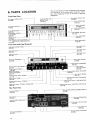
6. PARTS LOCATION
Front PanelView
F l u o r e s c e n ti n d i c a t o r t u b e
AAV-OO8
F l u o r e s c e n ti n d i c a t o r t u b e
AAV-OO7
K n o b ( F I L T E R ,F M ,
BRIGHT/DIM}
Knob (FUNCTION)
AAD-226
AAD.227
Knob (TUNING)
AAA-065
Knob (LOUDNESS)
AAD-227
Front panelassembly
AN8.861
Knob (SPEAKERS)
AAD.226
, UTING)
K n o b( M O D E M
AAD.139
' K n o b( V O L U M E )
AAB-238
Knob (BASS,TREBLE,
TURNOVER)
AAB-239
Woodencover
AMM-087
TONE,ADAPTOR,knob (POWER,
D U P L I C A T ET, A P EM O N I T O R )
AAD.139
K n o b( B A L A N C E )
AA8-239
Front View with PanelRemoved
Lamp with wires
AEL-069
P u s hs w i t c h ( B R I G H T / D l M )
ASG-230
Lamp with wires
AE L-095
Dual push switch
ASG-229
Lamp with wires
AEL-069
Lamp with wires
AEL-047
P h o n ei a c k ( P H O N E S )
AKN-O30
Tuning shaft assemblY
AXA-260
P u s hs w i t c h ( L O U D N E S S )
ASG-230
Leverswitch
( M U T I N G- 2 O d B }
ASK-152
R e m o t e s w i t c h ( S P E A K ER S )
ASX-137
, AL e v e r s w i t c h ( P O W E R )
-nsr-soz
Slide rotary switch
( B A S ST U R N O V E R }
ASE-125
2 - g a n gv a r i a b l e r e s i s t o r ( B A S S )
ACT-134
L e v e rs w i t c h ( T O N E )
ASK.152
2 - g a n gv a r i a b l er e s i s t o r ( T R E B L E )
ACT-134
Sliderotaryswitch (TREBLETURNOVER)
ASE-126
4 - g a n gv a r i a b l er e s i s t o r ( V O L U M E )
ACW-304
L e v e rs w i t c h ( M O D E )
A S K . 15 2
v a r i a b l er e s i s t o r ( B A L A N C E )
ACT-133
Remoteleverswitch (TAPEMONITOR)
ASX.131
R e m o t e l e v e rs w i t c h ( A D A P T O R , D U P L I C A T E )
ASX.128
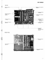
Rear PanelView
T e r m i n a l( I N P U T )
AKB-064
m i n a l ( P R E A M P O U T / P O W E RA M P l N )
AKB-063
Bar-antenna
ATB.624
T e r m i n a l( A M S T E R E O O U T )
AKB-076
AK
TE
e r- 0
m5i 4
n a l( S P E A K E R S )
-, A
I
AC socket (AC OUTLETS)
AKP-041
I
T e r m i n a(iA N T E N N A I
AKA-o13
16
AC power cord
ADG.O29
Terminal (TAPE, ADAPTOR)
AKB-063
r
s)<-39clct
c
Top Viw
S p e a k e r st e r m i n a l a s s e m b l y
GW3-222
R e c t i f i e ra s s e m b l y
AWR.211
E q u a l i z e ra s s e m b l y
AWM-226
Electrolytic capacitor
15 . O 0 0 pF , 7 1 V
ACH-210
Poweramplif ier assembly
AWH-097
Detector assembly
GWX.463
Tuner assembly
GWE-132
f
Indicatorassembly
AWV-OO8
\
Lamp socket
AKK-OO5
Lamp (wedge typel
AE L.029
/r
\t"Bottom View
r t;!
I
I
Tuner assembly
GWE-132
T o n e a m p l i fi e r a s s e m b l y
GWG-140
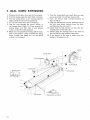
7. DIAL CORD STRINGING
1 . Removethe wooden cover and the front panel.
2 . Turn the tuning capacitor shaft fully clockwise.
3 . Fix the tuning drum to the tuning capacitor
shaft so that the set-screwis uppermost.
Tie one end of the dial cord to the spring.
5 . Pass the cord through the cutout section in
the tuning drum. Wind it ll2 turn around the
tuning drum, and then take it over pulleys
A, B, C, D and E in that sequence.
o . Wind the cord around the tuning shaft 3 times.
Passit over pully F, wind it around the tuning
drum 2 times, and finally tie it to the spring
so that it is tensioned.
4
7" Tum the tuning shaft and check that the cord
movessmoothly. Cut off any excesscord.
8. Tum the tuning shaft counter-clockwiseas
far as it will go.
9. Align the dial pointer with the starting point of
the dial scale (third division from the left),
and then passthe cord over it.
10. Check that the dial pointer is in line with the
starting point of the dial scale.
11. Finally apply the locking paint to the knot of
the cord and the dial pointer connection.
12. If the tension of the cord is weak, move the
springto the projection B.
S p r in g
T u n i n gd r u m
Tuningcapacitor
T u n i n gd r u m
B
T u n i n gs h a f t
E
\
D
D i a lp o i n t e r
1A
Dial pointerconnection
sx-3s|clcl
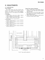
8. ADJUSTMENTS
8.1 AUDIOSECTION
PowerAmplifier
Turn VRS, VR5 (L) and VR4, VR6 (R) fully
around in the counter-clockwisedirection, but set
VR1(L) and VR2(R) to the center positions.
Without any load or input signal,tum the POWER
switch ON.
o DC Balance
1. Adjust VR1(L) for 0V(to within t30mV)
betweenterminal No.30 and ground.
2. Adjust VR2(R) for OV(to within t30mV)
betweenterminal No.29 and ground.
o Idle Cunent
1. Adjust VR3 (L) for 56mV between terminals
N o . 1 2 ( + )a n dN o . 1 1 ( - ) .
2. Adjust VR4 (R) for 56mV between terminals
N o . 9 ( + )a n d N o . 1 0 ( - ) .
3. Adjust VRb (L) for 70mV between terminals
N o . 1 2 ( + )a n d N o . 1 1 ( - ) .
4. Adjust VR6 (R) for 70mV between terminals
N o . 9 ( + )a n d N o . 1 0 ( - ) .
Output PowerIndicatorCalibration
1. Apply a IkHz signal to the POWER AMP IN
terminals (or any other input power amplifier
input terminals).
2. Adjust the level of this input signal so that
the voltage on the output terminals (SPEAKERS) read 8.95V(rms).
3. Adjust VR1(L) and VR2(R) so that the output power indicator read 10 watts.
Powertransformer
lndicator
assembly
V R s V R 3V R 1
vR2 VR4 VR6
r zir 3ozgr o
'g
F i g . 8 - 1 P o w e r a m p l i fi e r a d j u s t m e n t s
19
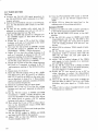
8 . 2 T U N E RS E C T I O N
FM Tuner
o Connect the FM SG (FM signal generator)to
the FM ANTENNA 300Q terminalsvia a 300O
dummy antenna.
o Switch the FUNCTION selectorto the FM position, the FM MUTING OFF switch to the OFF
position.
o L5 and L6 are coreless coils which may be
adjusted by extending one turn of coil out towardstuning capacitor(seeFig. 8-2).
1. Set the SX-3900 dial pointer to a frequencyin
the 106MHz region so that there will be no
input signal.
2. Rotate the N core of T2 so that the voltage
between no.B and no.7 terminals on the tuner
assemblyis reducedto DC 0V.
3. Next tune the dial pointer to 106MHz, and set
the FM SG outPut to 106MHz, 60 to 80dB
(modulation - 40OHz,t71kHz deviation).
4. Adjust TC1 so that the voltage betweenno.8
and no.7 terminals is reduced to DC 0V and
maximum readingof the SIGNAL indicator.
5. Then tune the dial pointer to 90MHz, and set
the FM SG output frequencyto 90MHz.
6. Rotate the L8 core so that the voltage between
no.B and no.? terminals is reducedto DC 0V
and maximum reading of the SIGNAL indicator.
7. Repeatsteps3 to 6 above.
8. Reset the FM SG output level to 20 30dB'
and adjust "1C2,"1C3,TC4 and T1 at 106MHz,
and L2, L5 and L6 at 90MHz in the samemanner as described in steps 3 to 7. These adjustments will ensure optimum sensitivity between
the two extreme frequencies.
9. Retune to a position with no input signal.
10. Rotate the A core of T2 so that the voltage
between no.8 and no.7 terminalsis reducedto
DC OV.
11. Set the FM SG output to 98MHz and 60dB
(modulation - 4O0Hz, x7lkHz deviation), and
tune the SX-3900 to this position (fine adjust
the tuning knob to ensure a DC 0V reading
betweenno.8 and no.7 terminals).
12. Then rotate the B core of T2 to reducedistortion in the demodulator output (TAPE REC
terminal) to minimum.
13. Repeatsteps9 to 12 aboveuntil both specifications are satisfactorilYmet.
14. Set the FM SG output to 98MHz and 60dB,
and tune the SX-3900to this position.
1-5.Adjust VR2 so that the SIGNAL indicator
(5-point display)reads"5".
20
16. Turn the FM MUTING OFF switch to the ON
position, and set the FM SG output level to
20d8.
17. Adjust VR1 to bring the input level to the
startingpoint of the muting operation.
MultiPlexDecoder
o Connect the MPX SG (FM multiplex generator)
to the FM SG externalmodulator terminal.
o Set the FM MUTING OFF switch to the OFF
position.
18. Set the FM SG output to 98MHz and 60dB
(unmodulated), and tune the SX-3900 to this
position (fine adjust the tuning knob to ensure
a DC 0V reading between no.S and no.7 terminals).
19. Adjust VRb to obtain a 76kHz signalat terminal no.6.
20. Set the FM SG output level to 60dB, and the
modulation mode to external. Then with the
MPX SG, set Main off, and pilot signal to
t7 .lkHz deviation.
21. Adjust VR4 to reduce leakageof the 19kHz
pilot signal (in both channels)to a minimum
(at TAPE REC terminals).
22.Set the FM SG output level to 80dB, the MPX
SG Main to 1kHz, L+R to t67.1kHz deviation,
and pilot signalto !7 .1kHz deviation.
23. Rotate the T1 core around by up to 90' in
either direction to reduce the demodulator
output (TAPE REC terminals) distortion to a
minimum.
24. Then set the FM SG output level to 60dB, the
MPX SG Main to 1-kHz,L (or R) to 133'75kHz
deviation, and pilot signal to x7.1kHz deviation.
25. Adjust VR4 to reduce crosstalkbetweenL and
R channelsto a minimum.
sx-3900
Crystal Detector
o Set the FM MUTING OFF switch to the OFF
position.
26. Set the FM SG output to 98MHz and 60dB
(unmodulated),and tune the SX-3900to this
position (fine adjust the tuning knob to ensure
a DC 0V reading between no.S and no.7 terminals of the tuner assembly).
27. Rotate the B core of T201 to obtain a reading
of DC 0V (within r30mV) between terminal
no.9 and ground.
28. Set the FM SG modulationto 40OHz,x7lkHz
deviation.
29. Rotate the A core of T201 to minimize AC
signallevel betweenno.9 and ground.
A
I
f f i t
rh
ffi
r-
ffi
|:I
Fig.8 2
A d j u s t m e n to f t h e t u n i n g c o i l s
AC voltmeter
D i s t o r t i o nm e t e r
@rr
L2
T o T A P ER E C
@
terminal
Oscilloscope
?,)-,
vR2
TC4 TC3 TC2
l@++-A
T2t^]l
l_9-D
T u n e ra s s e m b l y
M P X s i g n a lg e n e r a t o r
s--8
0--7
F M s i g n a gl e n e r a t o r
To FM
ANTENNA
3 0 0 S 2t e r m i n a l s
. OD)
I N ( E X TM
Fig.8 3
FM tuner adjustment
FrequencyDisplayCircuit
o The counter IC (PD5009) has been designedto
match FM ceramic filter IF offset (caused by
displacement of the central frequency) by
combination of the inputs (of H or L level)
applied to pin nos.3 & 4. The matchingIF offset
in the SX-3900 is determined accordingto the
combinationsof connectionsand disconnections
between the JP14 and JP15 jumper wires in the
equalizerassembly(AWM-226). Check that the
combinations shown in the table below have
been followed for the corresponding grades of
FM ceramic filters F1-F3 (5 ranks - color
coded).
PD5009
F M c e r a m i cf i l t e r s
(F1-F3)
Pin no.3
Red
Bl u e
Gray
Orange
Brown
If the SX-3900 frequency display reads
97.95MHz or 98.05MH2 when a 98.00MH2
signal is applied to the receiver, adjust TC1 so
that the displayreads98.00MH2correctly.
If an accurate 98.00MH2 input signalsource is
not available, tune the receiver to the nearest
known broadcasting station in the 98MHz region, and check that the station's frequency is
correctly displayed, adjusting TC1 if necessary.
AWM-226
Pin no.4
H
H
L
L
H
;
H
H
H
JP14
JP15
Cut
Cut
Connecl
Connect
Cut
Co1 n e c t
Cu
Cu
Cu
Cu
L=OV
JP
T;rl
B
_/
.T_T
:\
-rn I
JP
I n d i c a t o ra s s e m b l y
Equalizer
assembly
@
o
o
g
AD
@
F i g . 8 - 4 A d j u s t m e n t o f f r e q u e n c yd i s p l a y
@
six-39ocl
AM Tuner
o Connect the AM SG (AM signal generator)to
the AM ANTENNA terminal via 1kQ resistor'
o Switch the FUNCTION selectorto the AM position.
1. Set the SX-3900 dial pointer to 600kHz, and
the AM SG output to 600kHz, 100d8 (modulation 400H2,3O%).
2. Adjust the core of T3 to maximum demodulated output (at TAPE REC terminal).
3. Then set to 1400kH2, and set the AM SG output frequencyto 1400kHz also.
4. This time adjust TC6 to obtain maximum
demodulatedoutput (at TAPE REC terminal).
5. Set the SX-3900 dial pointer to 600kHz, and
the AM SG output to 600kHz,30d8.
6. Adjust the core of T3 to maximum demoduIated output (at TAPE REC terminal).
7. Then set to 1400kH2, and set the AM SG output frequencyto 1400kH2.
8. Adjust TC6 to obtain maximum demodulated
output (at TAPE REC terminal).
9. Repeatsteps5 to 8 above.
l-0. Set the SX-3900 dial pointer to 600kHz, and
the AM SG output frequencyto 600kHz.
11. Slide the bar-antennacoil along the core to
find the position which gives maximum demodulated output (at TAPE REC terminal).
12. Tune to 1400kH2, and set the AM SG output
frequencyto 1400kH2.
13. Adjust TC5 to obtain maximum demodulated
output (at TAPE REC terminal).
14. Repeatsteps10 to 13 as above.
15. Tune to 600kHz, and set the AM SG output
frequencyto 60OkHz.
16. Adjust T4 and F7 to obtain maximum demodulated output (at TAPE REC terminal).
Oscilloscope
Bar-antena
AC voltmeter
To TAPE
t e r mi n a l
A M s i g n a lg e n e r a t o r
To AM
A N T E N N A1 k f ) r e s i s t o r
terminal
Fig. 8-5 AM tuner adjustment
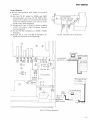
9 . S C H E M A T I CD I A G R A M
ExternalAppearanceof Transistorsand lCs
2SA905
2SC 91 5
2SA726S
Lot No
2SK34
Lor No---..Jri---fl
C)
hrr
l$
hre
++l
ryoe No
;iiJ
PA3007-A
..,*"-K)
I I D! l_r"o.
'o"-]$Jo/
i/|\\
d lJ\\
E
'Lot
-
2sA912
2SC1885
?
n
\r^'.
\qil,,. \
x${a''rl
-FsZ
D
3SK73
No
Loi No
Type No
",
/ il\
il|\
E Ll l l
c u
333#3f zsc177sA
' %-A(ll
Type No\
,Lot
No
-t
oss
-
HA1197
H A l 2 0 10
"Aruln+A
fi{+{il++ilfl
+{
2SA979
2S8682
Type No
2sK168
i^...\
-"0"^"" Jl\-I'l
I']
Lot No
Lo,No
\rfll
N
r,,.-\ffpf
2SA1076
25C2526
r-ot'o
il\/t'l
;!u
zSC1384
PA4006-A
At'0"*-{i_\
n"..--ltn]-l
f.-
"'*>ffi$.-'.
-l
.o,
"o---tl$J--t'0.
*o
}K
/ il\
E UII
C
2SC461
2SC535
25C2575
F.-
)
r-otno-_{$l
I i lLL-l-l-rYPe No
^*-)\P
ilil\
rype No
c--F\m
I at r'
No
_ Lot
l]ll\
2sA7so
2SC1400
H412017P
Nr
f nr\
I
<^s \ l l 6
Dot
*r\
l*\\4/rYe"
"-_'-,-'rsN I
}|iPl-t---.o,
B U \ \
c u
E
U
2SD313P
^..->f;i"/
iJ ll \\
a q l l
c u
ilu \iU
il tl
B v
N"
"o
TA7318P
Type No-
t l
Lot
No
PD5009
e
Lot No
2SA9o4A
2SC1914,A
5ut,r
h\
2SD313
N
)
r-"tr'r"--ld lf l I
lN tffi
r,*''----\Ul l/
ii IHr
/i il\\
l/lt\\
a u l l
c l l
24
Q$"
2SC1906
-
a
.nj44
IIJII\J|//
/ !\
Bull
2sAe78 ,i"rr*
2SA1100
5
.",,n"ffi
ull/
a2
2SA985A
,rO.""Nl
t*\t I
.,
" * * = - S'oss
HAl 201
NJM4558DV
Type No
rC\Yl
,ro"^o_ft\yl
n,rfiffpl--rot.,o
il\/tl
sltl
M54451P
t 4
JiiniJ[,J],
rM#+++#
H
)
11. PARTSLIST
NO?ES:
c W'henordering resrslors,first conuert resistanceualuesinto code form as shown in
the follo w ing examples.
Ex. 1 \Yhen there ere 2 effectiue digits (any digit apart from 0), such as 560 ohm
a n d ' 1 7 k o h m ( t o l e r a n c ei s s h o w n b y J = 5 % , a n d K : 1 0 o / " ) .
, 5 6 x 1 0 ' 5 6 1. . . .
. R D t / a PtSr 6 n J
560a
,17ksL
SA B J
4 7 x L U '
4 7 3 . . .
. R D I / n PA
05'2
0R5..
. RN2HOEtrK
1r)
010
nslP OEO 1{
Ex. 2 When there are 3 effectiue digits (such as in high precision metal filnt resis
tors).
5.62kst
o
562 x 10'
5 6 2I
RNI/aSR
tr6trtrr
I'he L
marh found on some componenl parts indicates the importance of the
safety factor of the part. Therefore, when replacing, be sure to use parts of
id e n t ic a I d esigna t ion.
Parts
Miscellaneous
Part No.
SEMICONDUCTORS
Part No.
25C2526
2 S A 10 7 6
Symbol & Description
o1-o4
o5-08
FUSES
Part No.
Svmbol & Description
I nrr-ros
FUl
FU2
F U 3 ,F U 4
r'i.AEK-1o2
A n er - r o o
1OA
2.54
1A
LAMPS
Part No.
A EL-029
A EL-069
A EL-095
AEL.O47
A E1 . 0 7 5
AEL-065
Symbol & Description
PLl-PL3
L a m p ( w e d g et y p e )
P L 4 , P L 5 , P L 7 , P L 8 L a m pw i t h w i r e s
PL6
Lamp with wires
PL9.PL10 Lampwith wires
P L 11
Lamp with wires
PLl2
L a m pw i t h w i r e s
PartNo.
Symbol & Description
f, nsr-soz
s17
A S X . 12 8
ASX.131
GWG-140
GWS-221
AWH-097
AWR.21O
GW5-222
T o n e a m p li f i e r a s s e m b l y
S w i t c ha s s e m b l y
P o w e r a m p l i fi e r a s s e m b l y
P o w e rs u p p l y a s s e m b l y
S p e a k e r tse r m i n a la s s e m b l y
GWS-223
GWK.146
AWR.211
Switch assembly
H e a d p h o n ejsa c k a s s e m b l y
R e c t i f i e ra s s e m b l y
OTHERS
PartNo.
Symbol & Description
.41ncc-oot
i\ 4rr-676
1, ntt-ozs
C1
T1
T2
T3
ATB-624
A nrp-o+r
i\ noc-ozs
AKB-076
AKH-O1O
AKK-O05
AKM.OO4
caMA 224K 250
SWITCHES
L e v e r( P O W E R )
R e m o t e l e v e r( A D A P T O R , D U P L I C A T E )
R e m o t e l e v e r( T A P E M O N I T O R )
Part No.
GWE.132
GWS-220
GWX-463
AWV.OOS
AWM-226
35
Symbol & Description
T u n e ra s s e m b l y
Switch assembly
Detectorassembly
I n d i c a t o ra s s e m b l y
Equalizea
r ssembly
C e r a m i c c a p a c i t o r 0 . 0 1/ 2 5 0 V
Powertransformer
Powertransformer
B a r - a n t e n n aa s s e m b l v
A C s o c k e t( A C O U T L E T S )
AC power cord
T e r m i n a l( A M S T E R E OO U T )
T r a n s i s t o rs o ck e t
Lamp socket
J u m p e rp l u g
c 2 ,c 3
(GWE-132)
Parts List of Tuner Assembly
CAPACITORS
Part No.
P . C .B O A R DA S S E M B L I E S
Symbol & Description
Symbol I Description
ACK-034
ACM-OO6
VC
TC1
50
C C D C HO T O D
c c D c H 0 1 0 c5 0
ccDcH 040c 50
c c D c H 1 2 0 J5 0
c c D C H 1 5 0 J5 0
c50
cl6
cl4
c11
wzl
T u n i n gc a p a c i t o r
C e r a m i ct r i m m e r
Symbol & Description
Part No.
1\ Rozevr rrr
L
R N % P OD ! D !
F
R 1 - R 1 1 , R 1 3 ,R 1 5 - R 2 2 , R 2 4 - R 2 9 ,
R31-R45, R47-R49, R52-R63, R65,
R 6 7 , R 7 0 - R 1 2 3 , R 1 2 5 ,R 1 2 8 - R 1 5 2
R12,R46,R126
R50,R51
R N % S O! ! ! N
F
R30
RD%PM !!!
c20
Symbol & Description
Part No.
J
ccDcH 330J 50
C C D C H 1 0 1 J5 0
ACG-018
C C D L H O S O D5 0
C C D R H 1 5 O J5 0
c52
c19
c11
C C D U J 1 2 O J5 0
C C D X L O B O D5 0
CCDSL 39OJ50
c c D S L 1 0 1 J5 0
C C D S L 1 5 1 J5 0
c 1 , c 8 , c 10
c89
c75
c24, C49
c 3 4 ,C 3 5
C K D Y B 1 O 2 K5 0
CKDYB 122K50
CKDYF 1032 50
c 1 5 , c 6 7 , C 6 8 ,C 8 2 ,C 9 1
c99
c 2 , c 5 , c 6 , c 1 3 , c 2 2 , c 2 3 , C 2 5 ,C 3 2 ,
c38, C41,C42,C44,C45,C81,C86,
c 8 7 , C 9 0 ,C 9 2 - C 9 5 ,C l 0 i , C l 0 7
3SK73
2SK34
2 S K 16 8
2 S C 19 0 6
2SC535-A
o1
02
0 3 , 0 15
Q4
o5
CKDYF 4]32 50
c 2 6 - C 2 9 ,C 3 1 ,C 3 7 ,C 3 9 ,C 4 0 ,
c46-C48, C74,C96,Cl 00, c104-c1 06,
c 10 8
c18
c9
H A 12 0 1
NJM4558DV
PA3007-A
P44006-A
HA1197
06, 07, 09
o8
010
011
412
CGB R68K 5OO
CGB R91J5OO
( C G B R 9 1K 5 O O )
C e r a m i c3 9 0 p / 5 0 V
SEMICONDUCTORS
Part No.
Symbol & Description
corvlA 153K 50
COMA 473K 50
C O S H3 3 1 J 5 0
cosH 751J 50
c o s H 15 2 J 5 0
c102
2 S C 19 19
25C2515
(2SC945A)
013
014,016-021,a24-416
c88
c 5 5 ,C 5 7
c 5 9 ,C 6 0
2 S A 110 0
(2SA733A)
o22, o23, o28-o35
o2l
c 10 3
c 6 3 ,C 6 4 ,C 7 0 , C t I
c65, C66
c 6 1 , C 6 2 ,C t 2
c79. C98
H A 1 2 0 10
CEANL R22M50
CEANL O1!M 50
CEANL 4R7M 50
C E A O l O Ms O L
CEA 3R3M 50L
MZ.061
D 1 ,D 2
CEA4R7M sOL
C E A l O O Ms O L
CEA 22AM 25L
C E A 4 7 O M1 O L
C E A 1 0 1 M1 O L
c91
c 3 3 , C 4 3 .C 5 6 ,C 6 9 ,C 8 5
c73
c80
c30, c76, c71
C E A 1 O 1 M2 5 L
C E A 2 2 1 M1 6 1
CEA331M1OL
C E A 4 7 1M 1 6 L
CEA 47OM25L
c36, C83,C84
(wz-061)
tJt333
D 3 , D s - D 17
11s24731
1SV69-03
D18
C O I L SA N D F I L T E R S
Part No,
Symbol & Description
c54
c 5 1 ,C 8 5
C 3 ,C 4 ,C 7 8
ATC-097
ATC-099
Arc-o72
L4, L7, L9-L13, Ll5, 116
C h o k ec o i l
F M a n t e n n ac o i l
L2
FM RF coil
L5, L6
F M o s c .c o i l
L8
RESISTORS
When ordering resistors,conuert the
resistanceualue itto code form, and
then rewrite the part no. as before.
Part No.
Symbol& Description
ATE-OO8
ATE-045
ATB.063
ATB-069
ATF-104"
T1
T2
T3
f4
F1-F3
Note
36
r24-O28
L t z
FM
FM
AM
AM
FM
IFT
DET
o s c .c o i l
lF coil
c e r a m i cf i l t e r
c92-048
c92-O49
ACP-056
ACP-0s5
ACT-133
V R 1 ,V R 3
VR2
VR4
VR5
VR6
S e m i - f i x e d( 4 7 k - B )
S e m i - f i x e d( 1 0 k - B )
S e m i - f i x e d( 2 2 k - B )
S e m i -ifx e d ( 6 . 8 k - B )
V a r i a b l e( B A L A N C E )
T h e F M c e r a m i cf i l t e r s ( A T F - 1 0 4 , s y m b o l n o s . F l - F 3 ) i n t h e
t u n e r a s s e m b l v( G W E - 13 2 ) h a s b e e n s e l e c t e do n t h e b a s i so f
their respective lF offset values (the degree of displacement
f r o m t h e c e n t e r l F ) . F i l t e r sa r e g r a d e di n t o 5 r a n k s ,t h e s eb e i n g
, r a y , b l u e ,a n d
i d e n t i f i e db y c o l o r c o d i n ga t t h e t o p ( r e d , o r a n g e g
b r o w n ) . W h e n r e p l a c i n gf i l t e r s , a l w a y s u s e f i l t e r s o f t h e s a m e
ACW-304
VR7
V a r i a b l e( V O L U M E )
colorcode.
W h e n p l a c i n g o r d e r s f o r t h e s e f i l t e r s , d e s i g n a t et h e g r a d e ( c o l o r )
a sw e l l a st h e p a r t n o .
sx-39clcl
Part No,
ATF-073
ATF-105
ATF-038
Symbol & Description
SEMICONDUCTORS
F 4 ,F 5
F6
F7
Part No.
F M l o w p a s sf i l t e r
A M c e r a m i cf i l t e r
AM lF filter
PartNo.
Symbol & Description
A S X . 13 3
A S X - 13 4
A S X - 13 O
ASK.152
S1
52
53
54. S5
R e m o t es l i d e( T A P E y I O N I T O R )
R e m o t es l i d e( D U P L I C A T E )
R e m o t es l i d e( A D A P T O R )
Svmbol & Description
Part No.
A S K - 15 2
A S E . 12 5
ASE-126
51
52
53
L e v e r( T O N E )
Slide rotary (200/400)
Slide rotary l2Kl4Kl
L e v e ri | V O D E ,M U T I N G )
Parts List of Switch Assembly(GWS-221)
OTHERS
Symbol & Description
Part No.
T e r m i n a l( A N T E N N A )
T e r m i n a l( T A P E , A D A P T O R )
A K A - O , I3
AKB-063
(GWS-220)
PartsList of Switch Assembly
Part No.
Symbol & Description
ASG-230
J
c o M A 4 7 3 K5 0
C C D S L1 5 1 J5 0
P u s hs w i t c h( L O U D N E S S )
56
R 3 0 1- R 3 0 6
c 3 0 1 ,c 3 0 2
c303, c304
PartsList of Tone Amplifier Assembly(GWG-140)
CAPACITORS
Part No.
Symbol & Description
c c D S L 1 0 1K 5 0
ccDSL 470K 50
c c D S L 4 7 1K 5 0
coMA 332J 50
COMA 123J50
c5, c6, c1 1, C12
C3, C4
c 1 3 ,C 1 4
coMA 124J50
CEANL R33M 50
C E A N L O l O M5 0
C E A N L l O O M5 0
C E A N LO R l M 5 0
c25, C26,C29,C30
c 1 5 ,C 1 6 ,C 1 9 ,C 2 0
, 34
c 1 7 ,C 1 8 ,C 2 1 , C 2 2C, 3 3 C
c35, C36
c 3 7 ,C 3 8
C E A 4 7 O M2 5 L
C E A 4 7 O M5 O L
CEAlOiM 1OL
CEANL4R7M 50
c9,c10
c39-C42
C7, C8
c1, c2
all
r1a
c23, C24,C27,C28
RESISTORS
When ordering resistors, conuert the
resistance ualue into code form, and
then rewrite the part no. as before.
Part No.
Symbol& Description
Note:
ACT-134
R D % P M! D !
HA120i7P
SWITCHES
SWITCHES
RDTaPM D!!
Symbol & Description
J
SWITCHES
Part No.
Symbol & Description
ASG-229
ASG-229
ASG-230
S4
JO
P u s h( F I L T E R )
P u s h( F M M U T I N G O F F )
P u s h( B R I G H T / D l M )
PartsList of PowerAmplifier Assembly(AWH-097)
CAPACITORS
Part No.
Symbol & Description
C E A N L4 R 7 M5 0
C C D S L2 2 1K 5 0
C C D S L4 7 O K5 0
ccDSL 470J50
c c D S L 3 9 0 K5 0
c o M A 3 3 2 K2 5 0
I c c o s r 1 0 1 Ks o o
C E A N PB 2 2 M5 0
ACG-009
CKDYB 472K 50
c o M A 8 2 3 K5 0
C E A4 7 1 M6 L
C E A1 0 1 M2 5 L
RESISTORS
cl13,Cl14
, 1 2 1, C 1 2 A
c 1 2 1, C 1 2 2 C
c 12 9 ,C 13 0
C 1 3 1 - C 1 3 4C e r a m i c 0 . 0 4 7 1 1 5 0 V
c 13 5 ,C 13 6
c 13 7 ,C l 3 8
c 13 9
c140
N o t e : When ordering resistors, conuert the
resistanceualue into code form, and
then rewrite the part no. as before.
Symbol& Description
PartNo.
V R 1 ,V R 2
V R 3 ,V R 4
V R 5 ,V R 6
ACP-035
ACP.O19
ACP-302
R D % P MI l A
c101,c102
c 10 3 , c 10 4
c 10 5 - c 1 0 8
c109,c110
cl11,C112
J
S e m i - f i x e(d3 3 0 k - B )
S e m i -i xf e d( 1 0 0 - B )
S e m i - f i x e(d1 0 0 k - B )
, 11 6 ,
R 1 0 1 - R 1 0 8R, 111 , R l 1 2 ,R 1 1 5 R
R119R
, 120F
. j 2 5 , R 1 2 6 ,R 1 4 5 ,R 1 4 6 ,
R 1 4 9 - R 1 5 2R, 1 5 7 R
, 1 5 8 ,R 1 6 7 - R 1 7 0 ,
, 199
R 1 7 5 - R 1 8 2R, 1 9 1 - R 1 9 4R, 1 9 7 R
, REBLE)
VR1, VR2
V a r i a b l e( B A S S T
R3-R40, R43,R44
37
Symbol & Description
Part No,
J
R D T a P M F! ! !
RSlP !tr! J
R D % P SI N I J
a RNlH !!t]
K
I nsznrn! K
t+
A ncru-t
R 1 0 9 ,R 1 1 0 ,R 1 1 3 ,R 1 1 4 ,R 1 1 7 ,R 1 1 8 ,
R123,R124,R|27-R142, Rl47 , R148,
R 1 5 3 - R 1 5 6 , R 15 9 - R 1 6 4 , R l t 1 - R 1 7 4
R 1 2 1, R 1 2 2 , R 1 4 3 , R 1 4 4
R196
R 1 8 7 ,R 1 8 8
R 1 8 9 ,R 1 9 0
R 1 8 3 - R 1 8 6 W i r ew o u n d ( t w i n )
O.4l l5W x 2
SEMICONDUCTORS
Symbol & Description
Part No.
0 1 0 1 ,0 1 0 2
2 S C 17 7 5 A - E *
o r 2 S C 17 7 5 A - F "
0 1 0 3 ,0 1 0 4
2 S A 9 7 9 - F*
or 2SA979-G*
" h f e o f 0 1 0 1 a n d O 1 0 2 s h o u l dh a v et h e E - r a n ki,1O 1 0 3 a n d
O 10 4 h a v et h e F - r a n k .
* h f e o f O 1 0 1 a n d O 1 0 2 s h o u l d h a v et h e F - r a n k it 0 1 0 3 a n d
Parts List of Indicator Assembly(AWV-008)
CAPACITORS
ACM-010
COMA 473J 50
C E A N L O l O M5 0
CEANL4R7M 50
coMA 332J 50
TCl
C E A 4 7 O M1 6 L
C E A 1 O 1 M2 5 L
CKDYF 1032 50
CKDYX 473M25
CEA471MlOL
c9
c10
0 1 0 5 ,0 1 0 6
0 1 0 7 ,o 1 0 8
raal
2SA750
o109,o110
o 1 11 , 0 1 1 2 ,0 1 1 7 , 4 1 1 8
2 S C 14 0 0
2SA905
2SA904A
2 S C 19 14 4
25C2575
0 1 1 3 ,0 1 1 4 , 0 1 1 9 , 0 1 2 0
0 11 5 , o 11 6
0121,4122
a123,4124
a 1 2 5 ,0 1 2 6 ,o ' , 3l 7 - o 1 3 9
ol tr
ccDcH020c50
CKDYF 473250
c c D S L 1 0 1K 5 0
C E A2 2 1 M1 6 L
C E AO l O Ms O L
RESISTORS
2 S C 13 8 4
o140
MZ-061
D101-D106
C3, C4
c5, c6
c 7 ,c 8
c12, c14, c17-c21 , c28
c 1 3 , c 1 5 , c 2 5 - c 2 7 , C 2 9 ,C 3 0
c 16 , C 3 2
ACP-OO7
RD%PIVI
l!tr
c24
c31
c 3 4 ,C 3 6
LJ3
c31-c43
N o t e : When ordering resistors, conuert the
resistance ualue into code form, and
then rewrite the part no. as before.
Symbol& Description
PartNo.
0 1 3 3 ,o 1 3 4
25C2275A-o**
or 25C2215A-P'*
o 1 3 5 ,o 1 3 6
2SA985A-O**
or 2SA985A-P"*
* * h f e o f O 1 3 3 - 0 1 3 6 s h o u l dh a v et h e s a m ev a l u e .
C e r a m i ct r i m m e r
c c D c H 1 0 1K 5 0
0 1 0 4 h a v et h e G - r a n k .
25C2291
2SA750
(2SA7265)
Symbol & Description
Part No.
J
VR1,VR2
Semi-fixed
R1-R33. R35-R63
SEMICONDUCTORS
PartNo.
T47318P-A
H A 12 0 10
M54451P
PD5009
Symbol & Description
o1
02, 03
o4
uc
06-010
(2SC945A)
2SC461-B
2-1K261
011
D 1- D 4
(wz-061)
STV2H
10E2
1S 15 5 5
( 15 2 0 7 6 )
D 1 0 9D, 1 1 0
D 11 1 , D 11 2 ,D 1 1 7D, 1 1 8
D113-D116
15247 1
MZ-150
, 132D
, 133
D129D
, 130D
D 13 1
(wz-150)
TH103-2
Th101.Th102
Part No,
Symbol & Description
RL1
ASR.068
PBZ3OPO6OFMC
r24-O28
AAV-OO7
L1, L2
V1
AAV.OOS
A S S - 0 11
VCZ3OPOSOFMC
v2
X1
C h o k ec o i l
F l u o r e s c e nitn d i c a t o rt u b e
F l u o r e s c e nitn d i c a t o rt u b e
Crystal resonator
Relay
CAPACITORS
Part No
CEANL4R7M 50
CEA 47OM50L
3A
Symbol & Description
PartsList of EqualizerAssembly(AWM-226)
OTHERS
Part No.
OTHERS
Symbol & Description
c3, c4, c29, C30
v t , v z , w t l , u t o
six-39clcl
Part No.
Symbol & Description
C E A 4 7 O M1 O L
CEA471M6L
C E A 2 2 O Ms O L
c 19 , C 2 0
c 9 , c 10
c25-C28
C C D S L2 2 O K 5 0
ccDSL 181K50
c c D s L 2 2 1K 5 0
coMA 683K 50
coPA i22G 50
c23, C24
c7, c8
C5, C6
c21,C22
c 1 5 ,C 1 6
coPA 183G50
COPA 683G 50
C K D Y F 1 O 3 Z5 0
CKDYF 4132 50
c 1 3 ,C 1 4
c 1 1, C 1 2
c31
Part No.
Symbol& Description
R1-R12, R15,R16,R21-R46
R 1 3 ,R 1 4 ,R 1 7 - R 2 0
R47
SEMICONDUCTORS
Part No.
Symbol & Description
2SA978
2SC17l5A
2 S C18 8 5
254912
01,02
03, 04
05, 06
07, 08
1S 15 5 5
( 15 2 0 7 6 )
D 1 ,D 2
Part No.
Symbol& Description
A nozpsrrrr .r
A n o z p v rr r l L
R D % P M! ! D
J
SEMICONDUCTORS
Part No.
2SK34
2 5 D 3 13 P
2SC1885
254912
2S8682
(258507)
Symbol & Description
01,02
UJ
a4
uc
vo
2SC1
9 15
2SA905
2SD33
1
25C2575
o7
o8
0 9 , o 11
010
1 Cl trRtr
D l , D 11
A roez
Symbol & Description
s - g a n gp u s h s w i t c h
ADU -ZZti
51
AKB-064
AKB.063
T e r m i n a (l I N P U T )
T e r m i n a l( P B E A l \ 4 PO U T / P O W E RA M P
tN)
PartsList of PowerSupply Assembly(AWR-210)
KZL-140
MZ-110
( w z - 11 0 )
MZ-130
(wz-130)
MZ-177
(wz-1771
f, nrr-ozs
Symbol & Description
C 2 ,C 1 4 ,C 1 8 ,C 1 9C e r a m i0c . 0 1 / 1 5 0 v
C 7 ,C 8
c5, c24
cl
ao
CAPACITORS
C E A 1 O 1 M2 5 L
C E A 4 7 O M5 0 L
C E A 4 7 O M6 3 1
C E A 4 7 1 M6 L
C E A2 2 1 M1 6 1
c16
c 1 2 ,C 1 3
c10,c11
Part No.
cl7
D13
D12
Symbol & Description
T1
H e a t e rt r a n s f o r m e r
PBZ3OP060FMC
VBZ30PO6OFMC
ACG-O04
C C D S L1 0 1K 5 0
C E A l O O M5 0 L
CEA 2R2M sOL
C E A 4 7 O M2 5 L
aaa
D2-D5, D7-D1 0
D6
D14
OTHERS
PartNo.
CAPACITORS
Part No.
R 3 , R 1 6 ,R 1 7
R11,R12
R23, R24
B4-R7
R1,R2, R8-R10, R13-R15, R18-R22,
R25,R26,R27
( 152076)
OTHERS
Part No.
c20, c21
cl5
c3. c4
RESISTORS
RSlP !D! J
R D % P SN l N J
wJz
c22
UO
When ordering resistors, conuert the
resistance ualue into code form, and
then rewrite the part no. as before.
Note
RESISTORS
R D % P MN I t r J
F
R N % P Ol l ! t r
R S 2 PD l D J
Symbol & Description
CEA 331M251
C E A l O O M6 3 L
C E A 4 7 1 M1 6 L
C E A 1 O 2 M3 5 L
CEA 221M8OL
When ordering resistors, conuert the
resistance ualue into code form, and
then rewrite the part no. as before.
Note:
Part No.
PartsList of Detector Assembly(GWX-463)
c c D S L 1 0 1 J5 0
c c D W K 1 5 0 K5 0
C K D Y B4 ] 1 K 5 0
CKDYF 103250
Symbol & Description
c201
c202
c204
c206
39
RESISTORS
When ordering resistors,conuert the
resistanceualue into code form, and
then rewrite the part no. as before.
Part No.
Symbol& Description
Note
RD%PM!N!
J
R 2 0 1- R 2 0 8
CAPACITORS
-B
2SC461
2-1K261
vt,vz
c3, c4
A ncc-otz
o201
D201,D202
OTHERS
Lf,
RESISTORS
Part No.
Symbol& Descriptiol__ =---
I ncru-oto
A ncru-ozg
R1
R2
Symbol & DescriPtion
PartNo,
ATE.O50
ASS-012*
r201
X1
FM DET
C r y s t a lr e s o n a t o r
T h e c r v s t a l r e s o n a t o r( A S S - 0 1 2 s, y m b o l n o . X 1 ) i n t h e d e t e c t o r
a s s e m b l v( G W X - 4 6 3 ) i s a v a i l a b l ei n 3 d i f f e r e n t t y p e s c o r r e s p o n d i n g t o t h e l F o f f s e t v a l u e so f t h e F M c e r a m i cf i l t e r s ( A T F - I 0 4 ,
s v m b o l n o s . F 1 - F 3 ) i n t h e t u n e r a s s e m b l y( G W E - 13 2 I . T h e s e
mav be identified by the different colored dots (red, blue,
o r a n g e ) a t t h e h e a d . W h e n r e p l a c i n g c r y s t a l r e s o n a t o r s ,c h e c k
t h a t t h e m a t c h i n g r e q u i r e m e n t sl i s t e d i n t h e f o l l o w i n g t a b l e a r e
met.
Crystal resonator (ASS-012)
Red
Blue
Orange
F M c e r a m i cf i l t e r ( A T F ' 1 0 4 )
0.01/150V
Ceramic
Electrolytic 15000/71V
0.01/125V
Ceramic
When ordering resistors, conuert the
resistanceualue into code form, and
then rewrite the part no. as before.
Note:
Symbol & DescriPtion
Part No.
Symbol & DescriPtion
Part No.
ACG-004
ACH-210
SEMICONDUCTORS
o
PartsList of RectifierAssembly(AWR-211)
W i r ew o u n d 3 . 3 / 2 0 W
Carbon composition
12.2Mly,wl
SEMICONDUCTORS
Part No.
Symbol & Description
A sstst
A sststn
D1
OTHERS
Part No.
Svmbol & Description
A nsn-oog
Araex-oot
F1
Rel ay
Temperature-sensitive fuse
)
R e d ( b l u eo r o r a n g ea l s op e r m i s s i b l e )
Blue(or brown)
O r a n g e( o r g r a y )
Parts List of SpeakersTerminal Assembly(GWS-222)
Part No.
Symbol & DescriPtion
T e r m i n a l( S P E A K E R S )
R e m o t es l i d es w i t c h
A nrr-osa
A S X - 13 7
(GWS-223)
Parts List of Switch Assembly
Part No.
Symbol & Description
Remote push switch
ASX-135
Jack Assembly(GWK-146)
PartsList of Headphones
Part No.
AKN-O3O
R S 2 P3 3 1J
40
Symbol & Description
P h o n e . i a c k( P H O N E S )
R 1 ,R 2
')
sx-39clct
12. EXPLODEDVIEW
Exterior Components
a
)
4
7
L
:N
l-\j\
,,P
,ngJ
\-i,/
I
l
| I
l c
o
NO?E'S:
o Pa,rtswithout parl number cannot
be supplied.
o ,he [' mark found on some
component parts indicates the importance
of the
safe.ty factor of the part. Therefore,^rnn:,
,nin"ing, be sure to useparts of
identical
designation.
Key No.
1.
2.
3.
4.
4-1.
4-2.
5.
6.
7.
B.
9.
10.
Part No.
DCK40P150FZK
AMM_087
vBz30P080FMC
AN8_861
AAD-226
AAD-227
WA92F140U100
Description
Key No.
part No.
1 1
Woodencover assembly
F r o n t p a n e la s s e m b l y
Knob A
Knob B
NK9OFUC
AAD-139
AAB-239
K n o b ( f o r l e v e rs w i t c h )
K n o b ( B A S S ,T R E B L E ,
AAB-238
444_065
T U R N O V E R ,B A L A N C E }
Knob (VOLUME)
Knob (Tuning)
12.
13.
14.
15.
Description
Food
vBz40POSoFMc
AEC-178
vrz4opl2oF^a
toot assemblv
Bottom plate
Interior ComPonents
NO?ES:
o Partswithout part number cannot be supplied'
of the
. in" A mark found on some component parts indicates the importance
safetyfactorofthepart.Therefore,whenreplacing,besuretousepartsofidentical
designation.
Part No.
Description
GWE.132
GWS-220
GWX.463
AWV-OO8
AWM.226
Tuner assemblY
Switch assemblY
Detector assemblY
lndicator assemblY
E q u a l i z e ra s s e m b l Y
T o n e a m p l i fi e r a s s e m b l Y
Switch assemblY
P o w e r s u p p l Ya s s e m b l Y
S p e a k e r st e r m i n a l a s s e m b l Y
10.
GWG.140
GWS-221
AWR-210
GW3-222
GWS.223
11.
12.
GWK.146
AWR-211
Key No.
1.
2.
4.
Description
ASX-131
Remote switch
Remotebelt
Remotebelt
Remotebelt
C e r a m i cc a p a c i t o r
ACG-001
AKP-041
ADG-029
Switch assemblY
54.
/i, 55.
AK8-076
ATT-676
AC socket (AC OUTLETS)
AC power cord
T e r m i n a l( G N D )
T e r m i n a l( A M S T E R E O O U T )
Powertransformer
H e a d p h o n e sj a c k a s s e m b l Y
R e c t i f i e ra s s e m b l Y
F u s eh o l d e r a s s e m b l y
Dial panel
Dial pointer
56.
I\ 57.
58.
A sg.
A oo.
ATA-624
4rT-675
AE L-029
AEK-106
AEK-102
B a r - an t e n n a
Powertrans{ormer
L a m p ( w e d g et Y P e )
F u s e( 1 A )
F u s e( 2 . 5 A )
17.
18.
19.
20.
Shaft cover A
Shaft cover B
Sidef rame L
Sideframe R
P a n e lf r a m e
A or.
62.
63.
64.
65.
AEK-305
AEL-069
AE L-O95
AE L-047
AE L-075
F u s e( 1 0 A )
Lamp with wires
Lamp with wires
Lamp with wires
Lamp with wires
21.
22.
23.
24.
25.
C e n t e rf r a m e
R e a rp a n e l
C e n t e rc h a n n e l
Tuner holder
Heat sink holder
66.
67.
68.
69.
70.
AEC-327
Strain relief
P la t e
Lamp socket
J u m p e rp l u g
Smoother
26.
T r a n s f o r m e rh o l d e r
S c a l eb o a r d h o l d e r L
S c a l eb o a r d h o l d e r R
E O h o l d e rA
E O h o l d e rB
71.
72.
73.
74.
75.
ABA-176
ABE-001
R e i n f o r c e dp l a t e
Ground plate
Acrylic board
Spacer A
Spacer B
76.
77.
7a.
79.
80.
ABN-050
NKgOFUC
wA92F140U100
wA35F100N080
AEC-525
Rod
Pulleyassembly
P u l l e y a s s e m b l yS
T u n i n gd r u m a s s e m b l Y
Tuning shaft assembly
81.
82.
83.
84.
85.
BBT3OPOSOFZK
vBz30P060FMC
PMT3OPO6OFZK
MTZ3OPlOOFZK
vBz30P080FMC
SPring
R e i n f o r c e dc h a n n e l
M o u n t i n gc l a m p
L e v e rs w i t c h ( P O W E R )
86.
87.
88.
89.
90.
PMZSOPOBOFMC
PMZ3OPO6OFMC
VBZ40P080FMC
PMZ3oP120FMC
Lamp with wires
AE L-065
o
i Q
14.
15.
lo.
28.
29.
30.
31.
32.
34.
36.
Jt.
JO.
40.
AXA-260
4 1'
42.
43.
tt
45.
42
A
46.
41.
48.
49.
50.
Part No.
A 51.
A, 52.
7.
u.
A,
Key No.
ASK.507
ASX-128
Remoteswitch
AKK-005
AKM-004
G r o u n d t e r m i n a l2 - P
Lamp holder
C a p a c i t o rc o v e r
S p e c i a ls c r e w
lnternal toothed lock washer
Union nut
Nylon rivet
HeatSink
/
\
fl
11
,.'r
NO?ES:
t Parts without part number cannot be supplied.
c The I
mark found on some component parts indicates the importance of the
safety factor of the part. Therefore, when replacing, be sure to use parts of identical
designation.
Key No.
1.
2.
3.
4.
5.
PartNo.
Description
VBZ3OPO6OFMC
Holder
VMH3OP120FMC
Socket stopper
25C2526
6.
7.
8.
9.
10.
2SA1076
AEC-488
AKH-010
11.
12.
13.
14.
15.
BBT3OPOSOFZK
16.
W A 3 3 F1 0 0 M 1 0 0
AWH-097
VBZ30P080FMC
STV2H
I n s u l a t o rw a f e r
T r a n s i s t o rs o c k e t
Heatsink
P A h o l d e rA
P A h o l d e rB
P o w e ra m p l i f i e r a s s e m b l y
13 . P A C K I N G
\...
;w
- --l
\ i
Parts List
Part No.
Description
1.
2.
3.
4.
5.
AR8-354
ADH-002
AHA-247
AHC-042
AH D-756
O p e r a t i n gi n s t r u c t i o n s
T-type FM antenna
Sidepad
I n s i d ep a c k i n g
6.
AHA-251
Rearpad
Key No.
40
P a c k i n gc a s e
( L / L )
SERVICE
m. 5I-484016
Date: l{ovsnber, 1983
INFORMATION
CDrrtoNEEFr
S/G
MooelrSX-J900/KU,
SUgJfCf ;
Addition of resistors
RgnSOru: For easier Idle
R200, R201
into Power Amp Assernbly.
current adjustment.
:
(Added) ---------)100rr
RDl/4PM1OlJNL
PRe
e:
Srnvrcr lvlnruunt[ A R T - 4 5 7 ]- - - - - -
S X - 3 9 0 0s e r i e s
21, 55
A p p l r c A B LS
Er R t R tN o , :
3 6 0 3 6 0 1290455L-
SX-39OO
/KU
s x - 3 9 0 0 / sc
POST CFtTCEBOX 1780
LONG BEACH, CALIFORNIA 90801
P H O N E :2 i 3 1 4 2 0 - 5 7 0 0 F A X : ( 2 ' 1 3 ) 4 2 0 ' 5 9 0 2
(J-lrc)
PIONEERELECTRONICS(USA INC.
TECHNICIALINFORMATICNCENTER
C)rqoNEEn
SFSs|OOS/G
The basic performanceof the S/G type is the sameas the KU type. This additionalservice
manualis applicableto the S/G type, pleaserefer to the KU type servicemanualwith exception
of this supplements.
SPECIFICATIONS
T h e s p e c i f i c a t i o nf osr S / G t y p e i s t h e s a m ea st h e K U t y p ee x c e p ft o r f o l l o w i n gs e c t i o n s ;
Miscellaneous
P o w e rR e q u i r e m e n t s
Powerconsumption.
W e i g h(tw i t h o u tp a c k a g e )
. A C 1 1 0 1 1 2 0 1 2 2 0 1 2 4(0sVw i t c h a b l e5)0 / 6 0 H 2
."310w
. 21kg
(46lb5 oz)
C O N T R A S TO F M I S C E L L A N E O U SP A R T S
of the
. The b marh found on some component parts indicates the importance
parts
identical
of
to
use
be
sure
replacing,
when
safety"factor of the part. Therefore,
designation.
SEMICONDUCTORS
Part No.
Description
Symbol
0 1- 0 4
05-08
T r an s is t o r
T r a nsi s t o r
Remarks
KU type
S/G type
25C2526
25A1076
2>VZAZO
2 S A 10 7 6
FUSES
Part No.
Description
Symbol
J" FU1
,\ FU2
F u s e( 1 0 A )
,\ rus
F u s e( 1 A )
F u s e( 1A )
F u s e( 5 A )
,i).FU4
A E K - l1 O
AEK-102
AEK-106
AEK-106
AEK-108
AEK.305
AEK-102
AEK.106
AEK.106
FUSe tZ.CA'
Remarks
S/G type
KU type
LAMPS
Part No.
Description
Symbol
Remarks
S/G type
KU type
AE L-029
AE L-029
AEL.O29
AE L-069
AEL.O69
AE L-029
AEL-029
AE L-029
AE L.069
AE L-069
wires
wires
wires
wires
wires
AE L-095
A E L-069
AE L-069
A E L-047
AEL.O47
AEL.Og5
AEL.069
AEL-069
AEL-047
AEL-047
Lamp with wires
Lamp with wires
AE L-075
AE L-065
AE L-075
AEL-065
PL1
PL2
PL3
PL4
PL5
L a m p ( w e d g et Y P e )
L a m p { w e d g et y p e )
L a m p ( w e d g et y p e )
Lamp with wires
Lamp with wires
PL6
PLl
PL8
PL9
PLlO
Lamp with
Lamp with
Lampwith
Lamp with
Lampwith
P L 11
PLl2
SWITCHES
Part No.
Symbol
A s tz
t\
Description
Lever (POWER)
R e m o t e l e v e r( A D A P T O R , D U P L I C A T E )
R e m o t el e v e r( T A P E M O N I T O R )
L i n e v o l t a g es e l e c t o r
KU type
ASK-507
ASX-128
ASX.131
Remarks
S/G type
ASK.508
ASX-128
ASX-131
AKX.063
'u
t
j
:i
:
P . C .B O A R DA S S E M B L I E S
Part No.
Description
Symbol
KU type
S/G type
Tuner assembly
Switch assembly
D e t e c t o ra s s e m b l y
I n d i c a t o ra s s e m b l y
E q u a l i z e ra s s e m b l y
GWE-132
GWS-220
GWX.463
AWV-OO8
AWM-226
GWE-132
GWS-220
GWX-463
AWV-OO8
AWM-226
Tone amplifier assembly
Switch assembly
P o w e ra m p l i f i e r a s s e m b l y
Powersupply assembly
S p e a k e r st e r m i n a l a s s e m b l y
GWG.140
GWS-221
AWH-097
AWR-210
GWS-222
GWG.140
GWS.221
AWH-097
AWR.21O
GWS-222
Switch assembly
H e a d p h o n e sj a c k a s s e m b l y
R e c t i fi e r a s s e m b l y
D e - e m p h a s ia
sssembly
GWS-223
GWK.146
AWR.211
GWS-223
GWK-146
AWR.214
AWS-147
Remarks
OTHERS
Part No.
Description
Symbol
ac1
C e r a m i cc a p a c i t o r
S/G type
ACG-001
coMA 224K 250
ATT.676
4TT.675
ATB.624
ACG-001
coMA 224K 250
ATT.682
4TT-681
ATB-624
AC socket (AC OUTLETS)
AC power cord
T e r m i n a l( A M S T E R E O O U T )
T r a n s i s t o rs o c k e t
Lamp socket
AKP-041
ADG-029
AKB-076
AKH.OlO
AKK.OOS
AKP.O41
ADG-049
AKB.O76
AKH.OlO
AKK-OOs
J u m p e rp l u g
AKM-OO4
AKM-OO4
c2,c3
T1
T2
T3
A
A
KU type
PowertransJormer
P o w e rt r a n s f o r m e r
B a r - an t e nn a
Remarks
PACKING
Symbol
Part No.
Description
KU type
S/G type
P a c k i n gc a s e
I n s i d ep a c k i n g
Sidepad
AHD-756
AHC-042
AHA-247
C a r d b o a r ds p a c e r
Rearpad
AHA-251
AHD-757
AHC-O42
AHA-247
AHB-089
AHA-251
Remarks
FURNISHED
PARTS
Symbol
Part No.
Description
KU type
O p e r a t i n gi n s t r u c t i o n s
T type FM antenna
ARB-354
ADH-OO2
S/G type
ARB.356
ADH-OO2
Remarks
RectifierAssembly(AWR-214)
FuseHolderAssembly(for S/G type)
De-emphasis
Assembly(AWS-I47)
50
PartsList of Rectifier Assembly(AWR-214)
CAPACITORS
SYmbol& DescriPtion
Part No.
C 1, C 2
C3,C4
C5
ACG-004
ACH-210
ACG-001
0.01/150V
Ceramic
Electrolytic 15000/71V
0.01/250V
Ceramic
RESISTOR
When ordering resistors, conuert the
resistance ualue into code form, and
then rewrite the part no. as before.
Part No.
Symbol & DescriPtion
Note:
ACN-019
Rl
Wire wound 3.3/20W
SEMICONDUCTORS
Part No.
J J I C I
b S t c t h
Symbol & Oescription
D1
D2
OTHERS
Part No.
ASR-069
AEX-0O1
Symbol & DescriPtion
RelaY
F1
use
T e m p e r a t u r e - s e n s i t i vf e
Assembly(AWS-147)
PartsList of De-emphasis
Part No.
50
Symbol & Description
c o s H 7 5 1 J5 0
cosH 152J50
C 1 ,C 2
c3, c4
ASH-015
51
S l i d es w i t c h
-,q
fir
. j
il
''
:l
.
:
,.
t
:!
' i .
rl
4-1 , Mesurc
1-chorrie,
Mesuno-ku.
Tokyo 153, Japen
PICINEEFI
ELECTFTCINIC
CCIFIPCIFIATICIN
U.!. FIC'NEEn
ELECTFICtNIea
E|5 Oxford OFive, Moonachie,
New Jerlsy
O7O74
U.S.A.
CC'F|FigllATlClN
FIC'NEEE
Belgium
ELECTFTCINIC IEUFICIPE
N.\,. Luitl€gen-Haven
I, POSO Antwerp,
Auatnalia
FfCINCEa
ELECTRCIJ{ICa
A|JaTF|ALIA
FTY- L?E'. 178-184
Bounddny Road. ElFeeside. Victonia 3195,