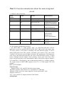
1
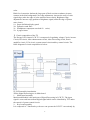
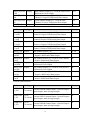
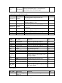
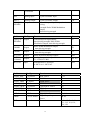
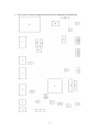
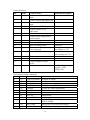
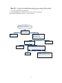
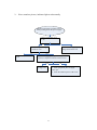
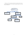
LCD TELEVISION SERVICE MANUAL CHASSIS LS03 Please read this manual carefully before service. 1 CONTENTS PartⅠ:Specification, feature and Composition ……………………………………3 PartⅡ: Function introduction about the main integrated circuit ………………..6 PartⅢ: Signal Processing Flow chart ….………………………………………….17 PartⅣ: Typical troubleshooting processing flowchart …………………………..22 Annex: Circuit schematic diagram 2 PartⅠ: Specification , feature and Composition Ⅰ. Main feature 1、Radio frequency input It can receive CATV signal. 2、AV input Convenient for watching a DVD player,VCR,pickup camera or other playback devices. 3、Scart input Convenient of receiving a high quality component signal from a DVD player. 4、YPbPr input Capable of receiving the high definition YPbPr signal in 480i, 480P, 576i, 576P, 720P, 1080i, and 1080P formats. 5、Scart output 6、VGA input a. Convenient to connect with a host computer. b. Use as a data display terminal. c. Connect the 3.5mm(diameter)audio jack to your computer’s soundcard to listen to stereo sound transmitted from your home computer. 7、Program & child lock function Capable of locking any program of the TV and the function button of the front panel. 8、Timer function 9、Blue background with noise reduction In AV、Scart and YPbPr modes, screen displays soft blue background , if there is no signal input. 10、 Multi Language on-screen display menu Text and graphical user interface makes the menu operation user-friendly. 11、 Power energy Saving mode(power management mode) When used as PC display terminal without PC signal output, the LCD TV will automatically power off within 30 Seconds and enter Power Energy Saving Mode. It will automatically startup again when it receives a signal from the PC.To start the TV manually with no signal press the number buttons or【 】/【P+】/【P-】 on the remote control. 12、Plug-and-play No additional software is needed when the product is used as computer terminal display. 13、Automatic picture’s quality adjustment 14、No flicker, no radiation, greenness and health 15、Auto on as time is set 16、Zoom mode(for19”,22”) Full-screen 、16:9、cinema、Subtitle 17、Legerity, convenient, low power consumption 18、Picture quality enhancement function Dynamic skin color correct: improve distort color in picture, make it near to real 3 color. Black level extension: darken the large part of black section to enhance pictures contrast in the dim background Color edge adjustment: increase the steep of color signal edge, make the edge of color transition more clearly. Brightness edge adjustment: increase edge gradient of brightness signal, make the edge of picture more clearer 19、Super definition display panel 20、Dynamic comb filter 21、Headphones output(not conclude 02 series) 22、8 page teletext Ⅱ. Circuit composition of the TV The Europe LS03 chassis LCD TV is composed of regulating voltage Circuit, inverter Circuit, RF circuit, video enhancement circuit, video Processing circuit, Power amplifier circuit, VGA circuit, system control circuit and key control circuit. The block diagram of circuit composition is below: Ⅲ. PCB assembly introduction All the Signal Processing are in Main board. 1、 Main board assembly Main board Module is the main part of Signal Processing in LCD TV. The input signal is converted into uniform digital signal which can be identified by TFT under the control of system control circuit. 2、 Key board assembly It is composed of 7 function keys. the user can operate the LCD TV conveniently by 4 using this assembly. 3、 Remote control receiving board assembly It is composed of a work indicator light and a remote receive head. The user use the remote control box by this module can operate the LCD TV conveniently and know the LCD TV work condition. 4、 Earphone output board assembly(not conclude 02 series) It is composed of a earphone outlet, user can Listen by earphoneconveniently. 5、 Inverter board assembly(include inverter circuit) The function of the inverter is supply power to light tube in TFT , and lighten the back lamp Unit of TFT module, so the user can see the image on TFT. 5 PartⅡ: Function introduction about the main integrated circuit Ⅰ. Main ICs and components Serial Name number 1 U4 2 U8 3 U9 model Main function MP1430DN-LF-Z PI5V330SQEX 24LC21AT/SN Liner voltage IC Video switch EEPROM(save display parameter information) EEPROM(save user control information) Audio processor Audio power amplifier single and multistandard alignment-free IF-PLL demodulators 4 U23 24LC32AT/SN 5 6 7 U11 U15 U19 STV-8217 TDA1517P TDA9886TS/V4 8 9 U17 U22 TDA5-E2I21RW2 MST718BE-LF RF tuner Processor with Video Decoder Ⅱ. The function introduction of main IC 1 The MST718BE is a high quality ASIC for NTSC/PAL/SECAM LCD-TV application. It receives analog NTSC/PAL/SECAM CVBS and S-Video inputs from TV tuners, DVD or VCR sources, including weak and distorted signals, as well as analog RGB input from GPS systems. Automatic gain control (AGC) and 10-bit 3-channel A/D converters provide high resolution video quantization. With automatic video source and mode detection,users can easily switch and adjust variety of signal sources. Multiple internal adaptive PLLs precisely extract pixel clock from video source and perform sharp color demodulation. Built-in line-buffer supports adaptive 2-D comb-filter, 2-D sharpening, and synchronization stabler in a condense manner. The output format of MST718BE supports 8-bit TTL or LVDS digital TFT-LCD modules. MST718 FEATURES: Video Decoder · Supports NTSC, PAL and SECAM video input formats ·2D NTSC and PAL comb-filter for Y/C separation of CVBS input ·Multiple CVBS and S-video inputs Supports Closed-caption and V-chip ·Supports Teletext 1.5 ·ACC, AGC, and DCGC (Digital Chroma GainControl) Analog Input 6 ·Supports RGB input format from PC,camcorders and GPS ·Supports YCbCr inputs from conventional videosource and HDTV ·Supports SCART – RGB + Fast Blank ·Supports video input 480i, 480p, 576i, 576p,720p, 1080i; RGB input resolution in 640x480,800x480, 800x600, 1024x768, and 1280x1024(SXGA) ·3-channel low-power 10-bit ADCs integration for YCbCr and RGB ·Supports RGB composite sync input (CSYNC),SOY, SOG, HSYNC, and VSYNC ·On-chip clock synthesizer and PLL ·Auto-position adjustment, auto-phase adjustment, auto-gain adjustment, and auto-mode detection Color Engine ·Brightness, contrast, saturation, and hue adjustment ·9-tap programmable multi-purpose FIR (Finite Impulse Response) filter ·Differential 3-band peaking engine ·Vertical peaking ·Spatial noise reduction ·Luminance Transient Improvement (LTI) ·Chrominance Transient Improvement (CTI) ·Black Level Extension (BLE) ·White Level Extension (WLE) ·Favor Color Compensation (FCC) ·3-channel gamma curve adjustment ·Independent 6 color of saturation, hue, and brightness control Scaling Engine/Panel Interface ·Supports digital panels up to 1366x768, and 1440x900 ·Supports single/dual 8-bit LVDS panel outputs ·Supports 8-bit TTL panel output ·Supports various displaying modes ·Supports horizontal panorama scaling Miscellaneous ·Built-in MCU ·3-wire serial bus interface for configuration setup ·Built-in step-down PWM circuits for input 2.5V ·Built-in internal OSD with 512 programmable fonts, 1、2 or 4 bit per pixel color,16-color palettes, and 12-bit color resolution ·Supports external OSD ·Support CVBS out ·Spread spectrum clocks ·Optional 3.3V / 5V output pads with programmable driving current ·128-pin PQFP package MST718 pin function: Analog Interface Pin Name Pin Type Function Pin 7 VMID VCLAMP REFM REFP PRINP Analog Input PRINM Analog Input PBINP Analog Input PBINM Analog Input SOY YINP Analog Input Analog Input YINM Analog Input BINP Analog Input BINM Analog Input SOGIN GINP Analog Input Analog Input GINM Analog Input RINP Analog Input RINM Analog Input C1INP Analog Input C1INM Analog Input YS1INP Analog Input YS1INM Analog Input C2INP Analog Input C2INM Analog Input YS2INP Analog Input YS2INM Analog Input CVBS1P CVBS1M Analog Input Analog Input Mid-Scale Voltage Bypass CVBS/YC Mode Clamp Voltage Bypass Internal ADC Bottom De-coupling Pin Internal ADC Top De-coupling Pin Analog Pr Input of HDTV Reference Ground for Analog Pr Input of HDTV Analog Pb Input of HDTV Reference Ground for Analog Pb Input of HDTV Sync-on-Y slicer input Analog Y Input of HDTV Reference Ground for Analog Y Input of HDTV Analog B Input of VGA Reference Ground for Analog B Input of VGA Sync-on-Green slicer input Analog G Input of VGA Reference Ground for Analog G Input of VGA Analog R Input of VGA Reference Ground for Analog R Input of VGA Analog Chroma Input for TV S-Video1 / Analog Composite Input of TV CVBS4 Reference Ground for Analog Chroma Input of TV S-Video1 / Analog Composite Input of TV CVBS4 Analog Luma Input of TV S-Video1 / Analog Composite Input of TV CVBS3 Reference Ground for Analog Luma Input of TV S-Video1 / Analog Composite Input of TV CVBS3 Analog Chroma Input for TV S-Video2 Reference Ground for Analog Chroma Input of TV S-Video2 Analog Luma Input of TV S-Video2 Reference Ground for Analog Luma Input of TV S-Video2 Analog Composite Input for TV CVBS1 Reference Ground for Analog Composite 8 2 3 4 5 7 8 9 10 11 12 13 14 15 16 17 18 19 20 22 23 24 25 26 27 28 29 30 31 CVBS2P Analog Input CVBS2M Analog Input Pin Name Input of TV CVBS1 Analog Composite Input for TV CVBS2 Reference Ground for Analog Composite Input of TV CVBS2 Pin Type VREXT_CDAC Analog Input HSYNCIN1 32 33 Function Pin Reference Current Generator, 820 ohm to Ground HSYNC / Composite Sync for VGA Input 1 116 Schmitt Trigger Input w/ 5V-tolerant VSYNCIN1 Schmitt Trigger VSYNC for VGA Input 1 Input w/ 5V-tolerant HSYNCIN2 Schmitt Trigger HSYNC / Composite Sync for VGA Input w/ Input 2 5V-tolerant VSYNCIN2 Schmitt Trigger VSYNC for VGA Input 2 Input w/ 5V-tolerant Digital Panel Output Interface Pin Pin Name Function Type CLKO Output Display Clock Output DEO Output Display Enable Output VSYNCO Output Vertical Sync Output HSYNCO Output Horizontal Sync Output BOUT[7]/LVB Output Blue channel Output [7] / LVDS B-Link Channel 0M 0 Negative Differential Data Output BOUT[6]/LVB Output Blue channel Output [6] / LVDS B-Link Channel 0P 0 Positive Differential Data Output BOUT[5]/LVB Output Blue channel Output [5] / LVDS B-Link Channel 1M 1 Negative Differential Data Output BOUT[4]/LVB Output Blue channel Output [4] / LVDS B-Link Channel 1P 1 Positive Differential Data Output BOUT[3]/LVB Output Blue channel Output [3] / LVDS B-Link Channel 2M 2 Negative Differential Data Output BOUT[2]/LVB Output Blue channel Output [2] / LVDS B-Link Channel 2P 2 Positive Differential Data Output BOUT[1]/LVB Output Blue channel Output [1] / LVDS B-Link Negative CKM Differential Clock Output 9 125 124 123 122 Pin 77 78 79 80 108 107 106 105 104 103 102 BOUT[0]/LVB CKP GOUT[7]/LVB 3M GOUT[6]/LVB 3P GOUT[5:4] Pin Name GOUT[3]/ LVA0M Output Output Output Output Pin Type Output GOUT[2]/ Output LVA0P GOUT[1]/ Output LVA1M GOUT[0]/ Output LVA1P ROUT[7:6] Output ROUT[5]/L Output VA2M ROUT[4]/L Output VA2P ROUT[3]/L Output VACKM ROUT[2]/L Output VACKP ROUT[1]/L Output VA3M ROUT[0]/L Output VA3P External OSD Interface Pin Name OSDR/GPI O_P30 OSDG/GPI O_P31 OSDB/GPI O_P32 Pin Type I/O w/ 5V-toleran t I/O w/ 5V-toleran t I/O w/ 5V-toleran t Blue channel Output [0] / LVDS B-Link Positive Differential Clock Output Green channel Output [7] / LVDS B-Link Channel 3 Negative Differential Data Output Green channel Output [6] / LVDS B-Link Channel 3 Positive Differential Data Output Green channel Output [5:4] Function Green channel Output [3] / LVDS A-Link Channel 0 Negative Differential Data Output Green channel Output [2] / LVDS A-Link Channel 0 Positive Differential Data Output Green channel Output [1] / LVDS A-Link Channel 1 Negative Differential Data Output Green channel Output [0] / LVDS A-Link Channel 1 Positive Differential Data Output Red channel Output [7:6] Red channel Output [5] / LVDS A-Link Channel 2 Negative Differential Data Output Red channel Output [4] / LVDS A-Link Channel 2 Positive Differential Data Output Red channel Output [3] / LVDS A-Link Negative Differential Clock Output Red channel Output [2] / LVDS A-Link Positive Differential Clock Output Red channel Output [2] / LVDS A-Link Channel 3 Negative Differential Data Output Red channel Output [0] / LVDS A-Link Channel 3 Positive Differential Data Output Function External OSD R-channel Input / General Purpose Input/Output; 4mA driving strength External OSD G-channel Input / General Purpose Input/Output; 4mA driving strength External OSD B-channel Input / General Purpose Input/Output; 4mA driving strength 10 101 99 98 97, 96 Pin 95 94 93 92 91, 90 89 88 87 86 85 84 Pin 73 74 75 FB/GPIO_ P33 I/O w/ External Fast-Blank Input / General Purpose 5V-toleran Input/Output; 4mA driving strength t 76 Switching Power and PWM Interface Pin Name Pin Type Function Switching Pulse Output for DC-DC PWMOUT2 Output Converter FB2 Analog Input Error Voltage Feedback Input Pin for PWM2; voltage = 1.2V SENSE2 Analog Input Sense Circuit Connection for PWM2 Switching Pulse Output for DC-DC PWMOUT1 Output Converter FB1 Analog Input Error Voltage Feedback Input Pin for PWM1; voltage = 1.2V SENSE1 Analog Input Sense Circuit Connection for PWM1 PGOOD Output Power Good Indicator Internal MCU Interface with Serial Flash Memory Pin Pin Type Name SAR2 Analog Input SAR1 Analog Input SAR0 Analog Input SCK Output SDI Output SDO Input w/ 5V-tolerant CSN Output GPIO_P0 I/O w/ 5V-tolerant 0-GPIO_ P07 INT Input SDA I/O w/ 5V-tolerant SCL Input w/ 5V-tolerant POWER_ Input w/ 5V-tolerant ON_RST N/CS Misc. Interface Pin Name RESET Pin Type Schmitt Trigger Input w/ Pin 38 39 40 41 42 43 44 Function Pin SAR Low Speed ADC Input 2 SAR Low Speed ADC Input 1 SAR Low Speed ADC Input 0 SPI Interface Sampling Clock SPI Interface Data-In SPI Interface Data-Out SPI Interface Chip Select 49 48 47 52 53 54 55 58-64, 83 General Purpose Input/Output; 4mA driving strength Interrupt Input for IR Receiver 3-Wire Serial Bus Data 3-Wire Serial Bus Clock Power On Reset Signal/Chip Selection for 3-wire Serial Function Hardware Reset; active high 11 65 66 67 68 Pin 72 5V-tolerant 121 XIN Analog Input Crystal Oscillator Input XOUT GPIO_P24 /PWMD3 Analog Output Output Crystal Oscillator Output General Purpose Input/Output; 4mA driving strength/ Pulse Width Modulation Output; 4mA driving strength Pin Name GPIO_P25 /PWMD4 Pin Type Output PWMD2 Output PWMD1 Output INT_OUT CVBSO1 /CVBSO2 MCUSEL Output Output Input Function General Purpose Input/Output; 4mA driving strength/ Pulse Width Modulation Output; 4mA driving strength Pulse Width Modulation Output; 4mA driving strength Pulse Width Modulation Output; 4mA driving strength Mode Detection Interrupt Output Analog Composite Output for TV CVBS1/CVBS2 Embedded MCU selection. 0: MCU on. 1: MCU off. 120 56 Pin 57 70 71 100 34, 115 109 Power Pins Pin Name Pin Type Function Pin AVDD_ADC AVDD_GMC AVDD_PWM AVDD_OPLL AVDD_CDAC AVDD_XTAL AVDD_MPLL VDDC 2.5V Power 5V Power 5V Power 2.5V Power 2.5V Power 5V Power 2.5V Power 2.5V Power 6, 21 35 37 113 117 118 127 50, 110 VDDP 3.3V/5V Power GND Ground ADC Power GMC Power PWM Power OPLL Power Current DAC Power XTAL Power MPLL Power Digital Core Power Digital Input/Output Power Ground 12 46, 82 1, 36, 45, 51, 69, 81, 111, 112, 114, 119, 126, 128 2 TDA9886 introduction: The TDA9885 is an alignment-free multistandard (PAL and NTSC) vision and sound IF signal PLL demodulator for negative modulation only and FM processing.The TDA9886 is an alignment-free multistandard (PAL, SECAM and NTSC) vision and sound IF signal PLL demodulator for positive and negative modulation,including sound AM and FM processing. FEATURES · 5 V supply voltage · Gain controlled wide-band Vision Intermediate Frequency (VIF) amplifier, AC-coupled · Multistandard true synchronous demodulation with active carrier regeneration: very linear demodulation,good intermodulation figures, reduced harmonics, and excellent pulse response · Gated phase detector for L and L-accent standard · Fully integrated VIF Voltage Controlled Oscillator(VCO), alignment-free, frequencies switchable for all negative and positive modulated standards via I2C-bus · Digital acquisition help, VIF frequencies of 33.4, 33.9,38.0, 38.9, 45.75, and 58.75 MHz · 4 MHz reference frequency input: signal from Phase-Locked Loop (PLL) tuning system or operating as crystal oscillator · VIF Automatic Gain Control (AGC) detector for gain control, operating as peak sync detector for negative modulated signals and as a peak white detector for positive modulated signals · External AGC setting via pin OP1 · Precise fully digital Automatic Frequency Control (AFC) detector with 4-bit digital-to-analog converter, AFC bits readable via I2C-bus · TakeOver Point (TOP) adjustable via I2C-bus or alternatively with potentiometer · Fully integrated sound carrier trap for 4.5, 5.5, 6.0, and 6.5 MHz, controlled by FM-PLL oscillator · Sound IF (SIF) input for single reference Quasi Split Sound (QSS) mode, PLL controlled · SIF-AGC for gain controlled SIF amplifier, single reference QSS mixer able to operate in high performance single reference QSS mode and in intercarrier mode, switchable via I2C-bus · AM demodulator without extra reference circuit · Alignment-free selective FM-PLL demodulator with high linearity and low noise · I2C-bus control for all functions · I2C-bus transceiver with pin programmable Module Address (MAD) · Four I2C-bus addresses via MAD. TDA9886 pin function: SYMBOL PIN DESCRIPTION 13 VIF1 VIF2 n.c. OP1 FMPLL DEEM AFD DGND n.c. AUD 1 2 3 4 5 6 7 8 TOP 9 SDA SCL 10 11 SIOMAD 12 n.c. n.c. n.c. TAGC REF VAGC n.c. CVBS n.c. AGND VPLL VP AFC OP2 n.c. 13 14 15 16 17 18 19 20 21 22 - SIF1 23 SIF2 24 n.c. n.c. - VIF differential input 1 VIF differential input 2 not connected output port 1; open-collector FM-PLL for loop filter de-emphasis output for capacitor AF decoupling input for capacitor digital ground not connected audio output tuner AGC TakeOver Point (TOP) for resistor adjustment I2C-bus data input and output I2C-bus clock input sound intercarrier output and MAD select with resistor not connected not connected not connected tuner AGC output 4 MHz crystal or reference signal input VIF-AGC for capacitor not connected composite video output not connected analog ground VIF-PLL for loop filter supply voltage AFC output output port 2; open-collector not connected SIF differential input 1 and MAD select with resistor SIF differential input 2 and MAD select with resistor not connected not connected 14 3 STV82x7 introduction The STV82x7 is a multistandard TV sound demodulator and audio processor.This chip performs automatic multistandard analog TV stereo sound identification and demodulation (no specific I²C programming is required). It offers various audio processing functions such as equalization, loudness, beeper, volume, balance, and surround effects. It provides a cost-effective solution for analog and digital TV designs. The STV82x7 is perfectly suited to current and future digital TV platforms, based on audio/video digital chips (STD2000, (DTV100 platform) and the future WorldWide iDTV one chip) which include an internal digital decoder (MPEG, Dolbyٛ Digital...). In the case where a Dolbyٛ Digital decoder is embedded in the audio/video digital chip, Virtual Dolbyٛ Digital could be obtained. For the CTV100/120 platform, the device is offered as an alternative solution to the first-generation chassis that uses the STV82x6. Features ● Single audio source processing: — IF source and/or analog stereo input (SCART) — one digital source with a maximum of 6 synchronous channels (5.1 is obtained across three I²S) ● SIF input signal with Automatic Gain Control (AGC) ● Digital Demodulator with automatic standard detection and demodulation for AM, FM mono, FM 2 carriers (German or Korean FM 2-carrier) and NICAM Analog matrix with: — five external inputs: four SCART inputs (2 VRMS capable) one analog mono input (0.5 VRMS) — one internal input from a digital matrix via a DAC — three external outputs (2 VRMS capable) — one internal output for the digital matrix (using an internal ADC) ● Digital matrix with: — three input modes (Demodulator/SCART, SCART only and I²S) — three stereo outputs (Loudspeakers, Headphone and SCART) ● High-end audio DAC ● S/PDIF output for connection with an external amplifier/decoder ● Internal multiplexer for the S/PDIF output (to share the internal S/PDIF output and the S/PDIF output generated by the external decoder of the digital broadcast) 9/149 ● Specific stand-by mode (Loop-through) ● Control by I²C bus (two I²C addresses) ● System PLL and Clock Generation using either a single quartz oscillator or a differential clock 15 4 TDA1517 introduction: The TDA1517 is an integrated class-B dual output amplifier in a plastic single in-line medium power package with fin (SIL9MPF), a plastic rectangular-bent single in-line medium power package with fin (RBS9MPF) or a plastic heat-dissipating dual in-line package (HDIP18). The device is primarily developed for multi-media applications. FEATURES · Requires very few external components · High output power · Fixed gain · Good ripple rejection · Mute/standby switch · AC and DC short-circuit safe to ground and VP · Thermally protected · Reverse polarity safe · Capability to handle high energy on outputs (VP = 0 V) · No switch-on/switch-off plop · Electrostatic discharge protection. TDA1517 pin function: SYMBOL PIN DESCRIPTION -INV1 1 non-inverting input 1 SGND 2 signal ground SVRR 3 supply voltage ripple rejection output OUT1 4 output 1 PGND 5 power ground OUT2 6 output 2 VP 7 supply voltage M/SS 8 mute/standby switch input -INV2 9 non-inverting input 2 16 PartⅢ: Signal Processing Flow chart This chapter mainly introduces analog signals process、video intensify process、TV system control process、TV supply system. 1、 IF/RF process Completed by TAF5-E2I21RW2 RF tuner, output IF signal. The Function of RF tuner is below: Pin 1 2 3 4 5 6 7 8 symbol AGC TU ADD SCL SDA BM BM NC 9 BTL function Auto gain control voltage The TV do not connect ground I2C bus(clock ) I2C bus(data ) +5V power supply +5V power supply Not connected +32V power supply,form 0~32V tune voltage Not connected IF signal output 10 NC 11 IF 2、 Image and sound process TDA9886 chip receives the IF signal separated from SAW filter, detects and decodes. Output CVBS analog signals from the 17 pin. Output TV-SIFP signal from 12 pin. CVBS analog signals is decoded inside of MST718BE chip. TV-SIFP signal is decoded inside of STV82x7 chip,then output the main channel L、R audio signal from 28,29 pin. 3、 Digital signal process The MST718BE receives analog NTSC/PAL/SECAM CVBS and S-Video inputs. It finishes the pixels ratio converting of input video signal、the image auto optimization process ,then process via memory buffer, scaler, chroma matrix circuitm, chroma look-up table, chroma space gain, etc. Output corresponding standard physical resolution digital color signal and corresponding sync, clock signal to TFT, control the TFT to display image correctly. 17 4、TV power supply system: 18 5、The location of main components and socket on mainboard and definition 19 Socket definition NO. Name 1 2 3 4 5 6 7 8 9 10 11 12 13 14 15 Connect object Connect outside SCART signal input Connect outside HD audio input Connect outside HD-YPbPr input Connect outside VGA input Connect outside VGA audio input Connect adapter outside power Connect inside supply power board module Connect display screen Connect display screen MST718 debug socket Connect remote control receiving board Connect TV K board Connect speaker Connect speaker Connect earphone output board Connect inverter 16 Description of Main component No. Name Element A U17 TDA5-E2I21RW2 B U11 STV82x7 C U14 Ams1117-1.8 E U15 TDA1517 F U20 K3953M G U18 K9656M H U19 TDA9886 I U8 P15V330 G U13 Ams1117-3.3 K U2 7808 L M U22 U9 MST718BE 24C21 Function description Not used Look circuit diagram, the fifth pin is 3.3V Look circuit diagram , the second pin is 3.3V +12V, +12V, backlight switch,GND, GND,GND Function description RF input, IF output Audio processor Low dropout voltage regulator Audio power amplifier IF Filter for Video Applications IF Filter for Audio Applications Analog signal processor Video switch Low dropout voltage regulator THREE TERMINAL POSITIVE VOLTAGE REGULATORS AD converter and format transformer EEPROM(save display parameter information) 20 N O P Q R S U24 U23 U4 U7 U6 U5 PS25LV040 24C32 MSP1430 Ams1117-2.5 Ams1117-3.3 4435(9435) T U1 IRF7314 Serial Flash Memory EEPROM(save display parameter information) Liner voltage IC Low dropout voltage regulator Low dropout voltage regulator ARX4435 Transceiver for Macair H009 Specification HEXFET Power MOSFET 21 PartⅣ: Typical troubleshooting processing flowchart Ⅰ. Typical troubleshooting flowchart 1、No anything(haven’t sound ,haven’t picture, haven’t indicator light),and no respondence to key,remote control. No answer,no respondence to key and remote control button NO Is outside adapter(or inside) output 12V normal? YES repair or change adapter The connection of Main board and key board ,remote control board is reliable or not? YES NO Connect the wire again Is U4,U6,U7 output port voltage normal? NO Check U4,U6,U7 Outside circuit YES Check each supply power pins voltage of U4,U6,U7 output to U22 are correct or not? YES NO 1、check peripheral parts of supply power pin . 2、check the soldered joint is OK or not. Change U22 22 2、 Have sound no picture, indicator light work normally indicator light work, but black screen when pressing down the power supply Observe back lamp is on or off YES NO U4,U6,U7 output voltage is normal or not? NO Check U4,U6,U7Outside circuit Check inverter supply power voltage and connect line YES Check each supply power pins voltage of U4,U6,U7 output to U22 are correct or not? YES Change U22 NO 1、check peripheral parts of supply power pin . 2、check the soldered joint is OK or not. 23 3、White screen: The reason of the troubleshoot is the signal electrode electrode haven’t working voltage. The TFT is always in transparent condition, so the whole screen is in white raster. VLCD of screen socket CON3(CON4) on main board is normal or not? NO YES Check the soldering of screen socket on main board is OK or not? Check Q5,U5,L6,L7,L8 etc related parts YES Switch signal source, use the oscillograph to check the signal input or not YES NO Check PCB copper connect line Check U22 peripheral circuit is normal or not ,change the trouble parts. 24 NO Patch solder