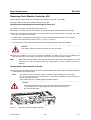
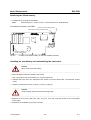
1
Test and Measurement Division Manual Vector Network Analyzer R&SZVB4 / ZVB8 1145.1010.06/10 Printed in the Federal Republic of Germany 1145.1084.82.01 1 Dear Customer, throughout this manual, the Vector Network Analyzer R&S® ZVB is abbreviated as R&S ZVB. R&S® is a registered trademark of Rohde & Schwarz GmbH & Co. KG Trade names are trademarks of the owners. 1145.1084.82.01 2 Safety Instructions This unit has been designed and tested in accordance with the EC Certificate of Conformity and has left the manufacturer’s plant in a condition fully complying with safety standards. To maintain this condition and to ensure safe operation, the user must observe all instructions and warnings given in this operating manual. Safety-related symbols used on equipment and documentation from R&S: Observe operating instructions 1. Weight indication for units >18 kg PE terminal Ground terminal The unit may be used only in the operating conditions and positions specified by the manufacturer. Unless otherwise agreed, the following applies to R&S products: IP degree of protection 2X, pollution severity 2 overvoltage category 2, only for indoor use, altitude max. 2000 m. The unit may be operated only from supply networks fused with max. 16 A. Unless specified otherwise in the data sheet, a tolerance of ±10% shall apply to the nominal voltage and of ±5% to the nominal frequency. 2. For measurements in circuits with voltages Vrms > 30 V, suitable measures should be taken to avoid any hazards. (using, for example, appropriate measuring equipment, fusing, current limiting, electrical separation, insulation). 3. If the unit is to be permanently wired, the PE terminal of the unit must first be connected to the PE conductor on site before any other connections are made. Installation and cabling of the unit to be performed only by qualified technical personnel. 4. For permanently installed units without built-in fuses, circuit breakers or similar protective devices, the supply circuit must be fused such as to provide suitable protection for the users and equipment. 5. Prior to switching on the unit, it must be ensured that the nominal voltage set on the unit matches the nominal voltage of the AC supply network. If a different voltage is to be set, the power fuse of the unit may have to be changed accordingly. 6. Units of protection class I with disconnectible AC supply cable and appliance connector may be operated only from a power socket with earthing contact and with the PE conductor connected. 095.1000 Sheet 17 Danger! Shock hazard Warning! Hot surfaces Ground Attention! Electrostatic sensitive devices require special care 7. It is not permissible to interrupt the PE conductor intentionally, neither in the incoming cable nor on the unit itself as this may cause the unit to become electrically hazardous. Any extension lines or multiple socket outlets used must be checked for compliance with relevant safety standards at regular intervals. 8. If the unit has no power switch for disconnection from the AC supply, the plug of the connecting cable is regarded as the disconnecting device. In such cases it must be ensured that the power plug is easily reachable and accessible at all times (length of connecting cable approx. 2 m). Functional or electronic switches are not suitable for providing disconnection from the AC supply. If units without power switches are integrated in racks or systems, a disconnecting device must be provided at system level. 9. Applicable local or national safety regulations and rules for the prevention of accidents must be observed in all work performed. Prior to performing any work on the unit or opening the unit, the latter must be disconnected from the supply network. Any adjustments, replacements of parts, maintenance or repair may be carried out only by authorized R&S technical personnel. Only original parts may be used for replacing parts relevant to safety (eg power switches, power transformers, fuses). A safety test must be performed after each replacement of parts relevant to safety. (visual inspection, PE conductor test, insulationresistance, leakage-current measurement, functional test). continued overleaf Safety Instructions 10. Ensure that the connections with information technology equipment comply with IEC950 / EN60950. 11. Lithium batteries must not be exposed to high temperatures or fire. Keep batteries away from children. If the battery is replaced improperly, there is danger of explosion. Only replace the battery by R&S type (see spare part list). Lithium batteries are suitable for environmentally-friendly disposal or specialized recycling. Dispose them into appropriate containers, only. Do not short-circuit the battery. 12. Equipment returned or sent in for repair must be packed in the original packing or in packing with electrostatic and mechanical protection. 095.1000 Sheet 18 13. Electrostatics via the connectors may dam- age the equipment. For the safe handling and operation of the equipment, appropriate measures against electrostatics should be implemented. 14. The outside of the instrument is suitably cleaned using a soft, lint-free dustcloth. Never use solvents such as thinners, acetone and similar things, as they may damage the front panel labeling or plastic parts. 15. Any additional safety instructions given in this manual are also to be observed. Certified Quality System Certified Environmental System ISO 9001 ISO 14001 DQS REG. NO 1954 QM DQS REG. NO 1954 UM Qualitätszertifikat Certificate of quality Certificat de qualité Sehr geehrter Kunde, Dear Customer, Cher client, Sie haben sich für den Kauf eines Rohde & Schwarz-Produktes entschieden. Hiermit erhalten Sie ein nach modernsten Fertigungsmethoden hergestelltes Produkt. Es wurde nach den Regeln unseres Qualitätsmanagementsystems entwickelt, gefertigt und geprüft. Das Rohde & SchwarzQualitätsmanagementsystem ist u.a. nach ISO 9001 und ISO14001 zertifiziert. You have decided to buy a Rohde & Schwarz product. You are thus assured of receiving a product that is manufactured using the most modern methods available. This product was developed, manufactured and tested in compliance with our quality management system standards. The Rohde & Schwarz quality management system is certified according to standards such as ISO9001 and ISO14001. Vous avez choisi d'acheter un produit Rohde & Schwarz. Vous disposez donc d'un produit fabriqué d'après les méthodes les plus avancées. Le développement, la fabrication et les tests respectent nos normes de gestion qualité. Le système de gestion qualité de Rohde & Schwarz a été homologué, entre autres, conformément aux normes ISO 9001 et ISO14001. Spare Parts Express Service Phone: +49 89 4129 - 12465 Fax: +49 89 41 29 - 13306 E-mail:[email protected] In case of urgent spare parts requirements for this Rohde & Schwarz unit, please contact our spare parts express service. Outside business hours, please leave us a message or send a fax or e-mail. We shall contact you promptly. 1007.9016 Adressen/Addresses FIRMENSITZ/HEADQUARTERS (Tel) Phone (Fax) Fax E-mail (Tel) +49 (89) 41 29-0 (Fax) +49 89 4129-121 64 [email protected] Rohde & Schwarz GmbH & Co. KG Mühldorfstraße 15 · D-81671 München Postfach 80 14 69 · D-81614 München Austria (Tel) +43 (1) 602 61 41-0 Rohde & Schwarz-Österreich Ges.m.b.H. (Fax) +43 (1) 602 61 41-14 Am Europlatz 3 [email protected] Gebäude B 1120 Wien Azerbaijan Rohde & Schwarz Azerbaijan Liaison Office Baku ISR Plaza, 5th floor 340 Nizami Str. 370000 Baku Bangladesh BIL Consortium Ltd. Corporate Office House-33, Road-4, Block-F Banani, Dhaka-1213 Barbados siehe / see Mexico Belarus siehe/see Ukraine Belgium Rohde & Schwarz Belgium N.V. Excelsiorlaan 31 Bus 1 1930 Zaventem Belize siehe / see Mexico Bermuda siehe/see Mexico BosniaHerzegovina siehe/see Slovenia Brazil Rohde & Schwarz Do Brasil Ltda. (Tel) +55 (11) 56 44 86 11 Av. Alfredo Egidio de Souza Aranha n° (general)·+55 177, (11) 56 44 86 25 (sales) 1° andar - Santo Amaro (Fax) +55 (11) 56 44 86 36 04726-170 Sao Paulo - SP [email protected] Brunei George Keen Lee Equipment Pte Ltd. #11-01 BP Tower 396 Alexandra Road Singapore 119954 Bulgaria Rohde & Schwarz Representation Office Bulgaria 39, Fridtjof Nansen Blvd. 1000 Sofia (Tel) +359 (2) 96 343 34 (Fax) +359 (2) 963 21 97 [email protected] (Tel) +1 (613) 592 80 00 (Fax) +1 (613) 592 80 09 [email protected] WERKE/PLANTS (Tel) +49 (8331) 108-0 Rohde & Schwarz Messgerätebau GmbH (Fax) +49 (8331) 108-11 24 Riedbachstraße 58 · D-87700 Memmingen Postfach 1652 · D-87686 Memmingen [email protected] Rohde & Schwarz GmbH & Co. KG (Tel) +49 (9923) 857-0 Werk Teisnach (Fax) +49 (9923) 857-11 74 Kaikenrieder Straße 27 · D-94244 Teisnach [email protected] Postfach 1149 · D-94240 Teisnach Rohde & Schwarz GmbH & Co. KG (Tel) +49 (2203) 49-0 Dienstleistungszentrum Köln (Fax) +49 (2203) 49 51-229 Graf-Zeppelin-Straße 18 · D-51147 Köln info.rsdc@rohdePostfach 98 02 60 · D-51130 Köln schwarz.com·[email protected] TOCHTERUNTERNEHMEN/SUBSIDIARIES Rohde & Schwarz Vertriebs-GmbH Mühldorfstraße 15 · D-81671 München Postfach 80 14 69 · D-81614 München (Tel) +49 (89) 41 29-137 74 (Fax) +49 (89) 41 29-137 77 [email protected] Rohde & Schwarz International GmbH Mühldorfstraße 15 · D-81671 München Postfach 80 14 60 · D-81614 München (Tel) +49 (89) 41 29-129 84 (Fax) +49 (89) 41 29-120 50 [email protected] Rohde & Schwarz Engineering and Sales GmbH Mühldorfstraße 15 · D-81671 München Postfach 80 14 29 · D-81614 München (Tel) +49 (89) 41 29-137 11 (Fax) +49 (89) 41 29-137 23 [email protected] R&S BICK Mobilfunk GmbH (Tel) +49 (5042) 998-0 Fritz-Hahne-Str. 7 · D-31848 Bad Münder (Fax) +49 (5042) 998-105 Postfach 2062 · D-31844 Bad Münder [email protected] Rohde & Schwarz FTK GmbH Wendenschlossstraße 168, Haus 28 D-12557 Berlin (Tel) +49 (30) 658 91-122 (Fax) +49 (30) 655 50-221 [email protected] Canada Rohde & Schwarz SIT GmbH Agastraße 3 D-12489 Berlin (Tel) +49 (30) 658 84-0 (Fax) +49 (30) 658 84-183 [email protected] Rohde & Schwarz Canada Inc. 555 March Rd. Kanata, Ontario K2K 2M5 Chile (Tel) +49 (2203) 49-5 23 25 (Fax) +49 (2203) 49-5 23 36 [email protected] Dymeq Ltda. Av. Larrain 6666 Santiago China Rohde & Schwarz China Ltd. Representative Office Beijing 6F, Parkview Center 2 Jiangtai Road Chao Yang District Beijing 100016 R&S Systems GmbH Graf-Zeppelin-Straße 18 D-51147 Köln Postfach 98 02 60 D-51130 Köln ADRESSEN WELTWEIT/ADDRESSES WORLDWIDE Albania siehe/see Austria Algeria Rohde & Schwarz Bureau d'Alger 5B Place de Laperrine 16035 Hydra-Alger (Tel) +213 (21) 48 20 18 (Fax) +213 (21) 69 46 08 Antilles (Neth.) siehe / see Mexico Argentina Precision Electronica S.R.L. Av. Pde Julio A. Roca 710 - 6° Piso 1067 Buenos Aires Australia Rohde & Schwarz (Australia) Pty. Ltd. Sales Support Unit 6 2-8 South Street Rydalmere, N.S.W. 2116 (Tel) +541 (14) 331 10 67 (Fax) +541 (14) 334 51 11 [email protected] (Tel) +61 (2) 88 45 41 00 (Fax) +61 (2) 96 38 39 88 [email protected] Rohde & Schwarz China Ltd. Representative Office Shanghai Room 807-809, Central Plaza 227 Huangpi North Road Shanghai 200003 Rohde & Schwarz China Ltd. Representative Office Guangzhou Room 2903, Metro Plaza 183 Tian He North Road Guangzhou 510075 (Tel) +994 (12) 93 31 38 (Fax) +994 (12) 93 03 14 [email protected] (Tel) +880 (2) 881 06 53 (Fax) +880 (2) 882 82 91 (Tel) +32 (2) 721 50 02 (Fax) +32 (2) 725 09 36 [email protected] (Tel) +656 276 06 26 (Fax) +656 276 06 29 [email protected] (Tel) +56 (2) 339 20 00 (Fax) +56 (2) 339 20 10 [email protected] (Tel) +86 (10) 64 31 28 28 (Fax) +86 (10) 64 37 98 88 [email protected] (Tel) +86 (21) 63 75 00 18 (Fax) +86 (21) 63 75 91 70 [email protected] (Tel) +86 (20) 87 55 47 58 (Fax) +86 (20) 87 55 47 59 [email protected] Adressen/Addresses China Rohde & Schwarz China Ltd. Representative Office Chengdu Unit G, 28/F, First City Plaza 308 Shuncheng Avenue Chengdu 610017 (Tel) +86 (28) 86 52 76 06 (Fax) +86 (28) 86 52 76 10 [email protected] Rohde & Schwarz China Ltd. Representative Office Xian Room 603, Jin Xin International No. 99 Heping Road Xian 710001 (Tel) +86 (29) 87 41 53 77 (Fax) +86 (29) 87 20 65 00 [email protected] Germany siehe / see Mexico Croatia siehe/see Slovenia Cuba siehe / see Mexico Cyprus Hinis Telecast Ltd. Agiou Thoma 18 Kiti Larnaca 7550 Czech Republic Rohde & Schwarz Praha, s.r.o. Hadovka Office Park Evropská 2590/33c 16000 Praha 6 Zweigniederlassung Mitte, Geschäftsstelle (Tel) +49 (2203) 807-0 Köln (Fax) +49 (2203) 807-650 Niederkasseler Straße 33 · D-51147 Köln [email protected] Postfach 900 149 · D-51111 Köln Denmark Egypt Rohde & Schwarz Danmark A/S Ejby Industrivej 40 2600 Glostrup (Tel) +45 (43) 43 66 99 (Fax) +45 (43) 43 77 44 [email protected] U.A.S. Universal Advanced Systems 31 Manshiet El-Bakry Street Heliopolis 11341 Cairo El Salvador siehe/see Mexico Estonia Rohde & Schwarz Danmark A/S Estonian Branch Office Narva mnt. 13 10151 Tallinn Finland Rohde & Schwarz Finland Oy Taivaltie 5 01610 Vantaa France Rohde & Schwarz France Immeuble "Le Newton" 9-11, rue Jeanne Braconnier 92366 Meudon La Forêt Cédex (Tel) +20 (2) 455 67 44 (Fax) +20 (2) 256 17 40 [email protected] Germany (Tel) +33 (2) 99 51 97 00 (Fax) +33 (2) 99 51 98 77 Zweigniederlassungen der Rohde & Schwarz Vertriebs-GmbH/Branch offices of Rohde & Schwarz Vertriebs-GmbH Zweigniederlassung Nord, Geschäftsstelle (Tel) +49 (30) 34 79 48-0 Berlin (Fax) +49 (30) 34 79 48 48 Ernst-Reuter-Platz 10 · D-10587 Berlin [email protected] Postfach 100620 · D-10566 Berlin Zweigniederlassung Süd, Geschäftsstelle Nürnberg Donaustraße 36 D-90451 Nürnberg (Tel) +49 (911) 642 03-0 (Fax) +49 (911) 642 03-33 [email protected] Kop Engineering Ltd. P.O. Box 11012 3rd Floor Akai House, Osu Accra North (Tel) +233 (21) 77 89 13 (Fax) +233 (21) 701 06 20 [email protected] Greece Mercury S.A. 6, Loukianou Str. 10675 Athens (Tel) +302 (10) 722 92 13 (Fax) +302 (10) 721 51 98 [email protected] Guatemala siehe/see Mexico Guiana siehe / see Mexico Haiti siehe / see Mexico Honduras siehe/see Mexico Hong Kong Electronic Scientific Engineering 9/F North Somerset House Taikoo Place 979 King's Road, Quarry Bay Hong Kong Hungary Rohde & Schwarz Budapesti Iroda Váci út 169 1138 Budapest Iceland siehe/see Denmark India Rohde & Schwarz India Pvt. Ltd. 244, Okhla Industrial Estate Phase - III New Delhi 110 020 (Tel) +91 (11) 26 32 63 81 (Fax) +91 (11) 26 32 63 73 [email protected] Rohde & Schwarz India Pvt. Ltd. Bangalore Office No. 24, Service Road, Domlur 2nd Stage Extension Bangalore - 560 071 (Tel) +91 (80) 535 23 62 (Fax) +91 (80) 535 03 61 [email protected] Rohde & Schwarz India Pvt. Ltd. Hyderabad Office 302 & 303, Millennium Centre 6-3-1099/1100, Somajiguda Hyderabad - 500 016 (Tel) +91 (40) 23 32 24 16 (Fax) +91 (40) 23 32 27 32 [email protected] (Tel) +358 (207) 60 04 00 (Fax) +358 (207) 60 04 17 [email protected] Niederlassung/Subsidiary Rennes 37 Rue du Bignon Bâtiment A 35510 Cesson Sévigné (Tel) +49 (89) 41 86 95-0 (Fax) +49 (89) 40 47 64 [email protected] Ghana (Tel) +372 (6) 14 31 23 (Fax) +372 (6) 14 31 21 [email protected] (Tel) +33 (0) 141 36 10 00 (Fax) +33 (0) 141 36 11 11 [email protected] Zweigniederlassung Süd, Geschäftsstelle München Mühldorfstraße 15 · D-81671 München Postfach 80 14 69 · D-81614 München Zweigniederlassung Mitte, Geschäftsstelle (Tel) +49 (6102) 20 07-0 Neu-Isenburg (Fax) +49 (6102) 20 07 12 Siemensstraße 20 D-63263 Neu-Isenburg [email protected] Postfach 16 51 D-63236 Neu-Isenburg (Tel) +357 (24) 42 51 78 (Fax) +357 (24) 42 46 21 [email protected] (Tel) +420 (2) 24 31 12 32 (Fax) +420 (2) 24 31 70 43 [email protected] (Tel) +49 (228) 918 90-0 (Fax) +49 (228) 25 50 87 [email protected] Zweigniederlassung Nord, Geschäftsstelle (Tel) +49 (40) 38 61 83 - 00 Hamburg (Fax) +49 (40) 38 61 83 - 20 Vierenkamp 6 D-22423 Hamburg [email protected] Rohde & Schwarz China Ltd. (Tel) +86 (755) 82 03 11 98 Representative Office Shenzhen (Fax) +86 (755) 82 03 30 70 Room 1901, Central Business [email protected] No. 88 Fuhua Yilu Futian District Shenzhen 518026 Costa Rica Zweigniederlassung Büro Bonn Josef-Wirmer-Straße 1-3 · D-53123 Bonn Postfach 140264 · D-53057 Bonn (Tel) +852 (25) 07 03 33 (Fax) +852 (25) 07 09 25 [email protected] (Tel) +36 (1) 412 44 60 (Fax) +36 (1) 412 44 61 [email protected] Adressen/Addresses India Indonesia Iran Rohde & Schwarz India Pvt. Ltd. Mumbai Office B-603, Remi Bizcourt, Shah Industrial Estate, Off Veera Desai Road Andheri West Mumbai - 400 058 (Tel) +91 (22) 26 30 18 10 (Fax) +91 (22) 26 73 20 81 [email protected] PT Rohde & Schwarz Indonesia Graha Paramita 5th Floor Jln. Denpasar Raya Blok D-2 Jakarta 12940 (Tel) +62 (21) 252 36 08 (Fax) +62 (21) 252 36 07 [email protected]·[email protected] Rohde & Schwarz Iran Liaison Office Tehran Groundfloor No. 1, 14th Street Khaled Eslamboli (Vozara) Ave. 15117 Tehran (Tel) +98 (21) 872 42 96 (Fax) +98 (21) 871 90 12 [email protected] Ireland siehe/see United Kingdom Israel Eastronics Ltd. Measurement Products 11 Rozanis St. P.O.Box 39300 Tel Aviv 61392 (Tel) +972 (3) 645 87 77 (Fax) +972 (3) 645 86 66 [email protected] J.M. Moss (Engineering) Ltd. Communications Products 9 Oded Street P.O.Box 967 52109 Ramat Gan (Tel) +972 (3) 631 20 57 (Fax) +972 (3) 631 40 58 [email protected] Rohde & Schwarz Italia S.p.a. Centro Direzionale Lombardo Via Roma 108 20060 Cassina de Pecchi (MI) (Tel) +39 (02) 95 70 41 (Fax) +39 (02) 95 30 27 72 [email protected] Rohde & Schwarz Italia S.p.a. Via Tiburtina 1182 00156 Roma (Tel) +39 (06) 41 59 81 (Fax) +39 (06) 41 59 82 70 [email protected] Italy Jamaica siehe / see Mexico Japan Rohde & Schwarz Japan K.K. Tokyo Office 711 Bldg., Room 501 (5th floor) 7-11-18 Nishi-Shinjuku Shinjuku-ku Tokyo 160-00023 Jordan (Tel) +81 (3) 59 25 12 88 (Fax) +81 (3) 59 25 12 90 [email protected] Rohde & Schwarz Japan K.K. Shin-Yokohama Office KM Daiichi Bldg., 8F 2-13-13 Kouhoku-ku Yokohama-shi Kanagawa 222-0033 (Tel) +81 (4) 54 77 35 70 Rohde & Schwarz Japan K.K. Osaka Office TEK Dai 2 Bldg., 8F 1-13-20 Esaka-shi Suita-shi Osaka-fu 564-0063 (Tel) +81 (6) 63 10 96 51 Jordan Crown Engineering & Trading Co. Jabal Amman, Second Circle Youssef Ezzideen Street P.O.Box 830414 Amman, 11183 (Tel) +962 (6) 462 17 29 (Fax) +962 (6) 465 96 72 [email protected] Kazakhstan Rohde & Schwarz Kazakhstan Representative Office Almaty Pl. Respubliki 15 480013 Almaty Kenya Excel Enterprises Ltd Dunga Road P.O.Box 42 788 Nairobi Korea Rohde & Schwarz Korea Ltd. 83-29 Nonhyun-Dong, Kangnam-Ku (Tel) +7 (32) 72 67 23 54 (Fax) +7 (32) 72 67 23 46 [email protected] (Tel) +254 (2) 55 80 88 (Fax) +254 (2) 54 46 79 (Tel) +82 (2) 34 85 19 00 (Fax) +82 (2) 547 43 00 [email protected]·[email protected] Seoul 135-010 Kuwait Group Five Trading & Contracting Co. Mezzanine Floor Al-Bana Towers Ahmad Al Jaber Street Sharq Latvia Rohde & Schwarz Danmark A/S Latvian Branch Office Merkela iela 21-301 1050 Riga Lebanon Rohde & Schwarz Liaison Office Riyadh P.O.Box 361 Riyadh 11411 Netcom P.O.Box 55199 Op. Ex-Presidential Palace Horch Tabet Beirut (Tel) +965 (244) 91 72/73/74 (Fax) +965 (244) 95 28 [email protected] (Tel) +371 (7) 50 23 55 (Fax) +371 (7) 50 23 60 [email protected] (Tel) +966 (1) 465 64 28 Ext. 303 (Fax) +966 (1) 465 64 28 Ext. 229 [email protected] (Tel) +961 (1) 48 69 99 (Fax) +961 (1) 49 05 11 [email protected] Liechtenstein siehe/see Switzerland Lithuania Rohde & Schwarz Danmark A/S Lithuanian Branch Office Lukiskiu 5-228 2600 Vilnius Luxembourg siehe/see Belgium Macedonia NETRA Sarski odred 7 1000 Skopje Malaysia Rohde & Schwarz Malaysia Sdn Bhd (Tel) +60 (3) 20 94 00 33 Suite 10.04, Level 10, Wisma E&C (Fax) +60 (3) 20 94 24 33 No. 2 Lorong Dungun Kiri [email protected] Damansara Heights 50490 Kuala-Lumpur Malta Tektraco International Technology Ltd.(Tel) +356 (21) 37 43 00 or 37 80 88 121, B'Kara Road (Fax) +356 (21) 37 66 67 San Gwann SGN 08 [email protected] Mexico Rohde & Schwarz de Mexico S. de R.L. de C.V. German Centre Oficina 4-2-2 Av. Santa Fé 170 Col. Lomas de Santa Fé 01210 Mexico D.F. Moldava siehe/see Austria Nepal ICTC Pvt. Ltd. Hattisar, Post Box No. 660 Kathmandu (Tel) +370 (5) 239 50 10 (Fax) +370 (5) 239 50 11 [email protected] (Tel) +389 (2) 329 82 30 (Fax) +389 (2) 317 74 88 [email protected] (Tel) +52 (55) 85 03 99 13 (Fax) +52 (55) 85 03 99 16 [email protected] (Tel) +977 (1) 443 48 95 (Fax) +977 (1) 443 49 37 [email protected] Adressen/Addresses Netherlands Rohde & Schwarz Nederland B.V. Perkinsbaan 1 3439 ND Nieuwegein New Zealand Nichecom 1 Lincoln Ave. Tawa, Wellington (Tel) +31 (30) 600 17 00 (Fax) +31 (30) 600 17 99 [email protected] (Tel) +64 (4) 232 32 33 (Fax) +64 (4) 232 32 30 [email protected] Nicaragua siehe/see Mexico Nigeria Ferrostaal Abuja Plot 3323, Barada Close P.O.Box 8513, Wuse Off Amazon Street Maitama, Abuja Norway Rohde & Schwarz Norge AS Enebakkveien 302 B 1188 Oslo Oman Mustafa Sultan Science & Industry Co.LLC. Test & Measurement Products Way No. 3503 Building No. 241 Postal Code 112 Al Khuwair, Muscat Pakistan Siemens Pakistan 23, West Jinnah Avenue Islamabad Panama siehe/see Mexico Papua New Guinea siehe/see Australia Paraguay siehe/see Argentina Philippines Rohde & Schwarz (Philippines) Inc. Unit 2301, PBCom Tower 6795, Ayala Ave. cor. Herrera St. Makati City Poland Rohde & Schwarz SP.z o.o. Przedstawicielstwo w Polsce ul. Stawki 2, Pietro 28 00-193 Warszawa Portugal Rohde & Schwarz Portugal, Lda. Alameda Antonio Sergio 7-R/C - Sala A 2795-023 Linda-a-Velha Republic Dominican siehe/see Mexico Romania Rohde & Schwarz Representation Office Bucharest 89 Eroii Sanitari Bldv., sector 5 050472 Bucuresti Russian Federation Saudi Arabia (Tel) +234 (9) 413 52 51 (Fax) +234 (9) 413 52 50 [email protected] Saudi Arabia Gentec Haji Abdullah Alireza & Co. Ltd. P.O.Box 43054 Riyadh (Tel) +966 (1) 293 20 35 (Fax) +966 (1) 466 16 57 [email protected] SerbiaMontenegro Rohde & Schwarz Representative Office Belgrade Tose Jovanovica 7 11030 Beograd (Tel) +381 (11) 305 50 25 (Fax) +381 (11) 305 50 24 [email protected] Singapore Rohde & Schwarz Regional Headquarters Singapore Pte. Ltd. 1 Kaki Bukit View #05-01/02 Techview Singapore 415 941 Rohde & Schwarz Systems & Communications Asia Pte Ltd Service 1 Kaki Bukit View #04-01/07 Techview Singapore 415 941 (Tel) +47 (23) 38 66 00 (Fax) +47 (23) 38 66 01 [email protected] (Tel) +968 63 60 00 (Fax) +968 60 70 66 [email protected] (Tel) +92 (51) 227 22 00 (Fax) +92 (51) 227 54 98 [email protected] (Tel) +65 68 46 37 10 (Fax) +65 68 46 00 29 [email protected] Slovak Republic Specialne systemy a software, a.s. Svrcia ul. 3 841 04 Bratislava 4 Slovenia Rohde & Schwarz Representative Office Ljubljana Tbilisijska 89 1000 Ljubljana South Africa Protea Data Systems (Pty.) Ltd. Communications and Measurement Division Private Bag X19 Bramley 2018 (Tel) +27 (11) 719 57 00 (Fax) +27 (11) 786 58 91 [email protected] Protea Data Systems (Pty.) Ltd. Cape Town Branch Unit G9, Centurion Business Park Bosmandam Road Milnerton Cape Town, 7441 (Tel) +27 (21) 555 36 32 (Fax) +27 (21) 555 42 67 [email protected] (Tel) +63 (2) 753 14 44 (Fax) +63 (2) 753 14 56 (Tel) +48 (22) 860 64 94 (Fax) +48 (22) 860 64 99 [email protected] (Tel) +65 68 46 18 72 (Fax) +65 68 46 12 52 Spain (Tel) +351 (21) 415 57 00 (Fax) +351 (21) 415 57 10 [email protected] (Tel) +421 (2) 65 42 24 88 (Fax) +421 (2) 65 42 07 68 [email protected] (Tel) +386 (1) 423 46 51 (Fax) +386 (1) 423 46 11 [email protected] Rohde & Schwarz Espana S.A. Salcedo, 11 28034 Madrid (Tel) +34 (91) 334 10 70 (Fax) +34 (91) 729 05 06 [email protected] Rohde & Schwarz Espana S.A. Av. Princep d'Astúries, 66 08012 Barcelona (Tel) +34 (93) 415 15 68 (Fax) +34 (93) 237 49 95 [email protected] Sri Lanka Dynatel Communications (PTE) Ltd. 451/A Kandy Road Kelaniya Sudan SolarMan Co. Ltd. P.O.Box 11 545 North of Fraouq Cementry 6/7/9 Bldg. 16 Karthoum Rohde & Schwarz International GmbH (Tel) +7 (095) 745 88 50 to 53 119180, Yakimanskaya nab., 2 (Fax) +7 (095) 745 88 54 Moscow [email protected] Sweden Rohde & Schwarz Sverige AB Flygfältsgatan 15 128 30 Skarpnäck (Tel) +46 (8) 605 19 00 (Fax) +46 (8) 605 19 80 [email protected] Rohde & Schwarz International GmbH (Tel) +966 (1) 293 2035 Liaison Office Riyadh (Fax) +966 (1) 466 1657 c/o Haji Abdullah Alireza Co. Ltd. [email protected] P.O.Box 361 Riyadh 11411 Switzerland Roschi Rohde & Schwarz AG Mühlestr. 7 3063 Ittigen (Tel) +41 (31) 922 15 22 (Fax) +41 (31) 921 81 01 [email protected] Syria Electro Scientific Office Baghdad Street Dawara Clinical Lab. Bldg P.O.Box 8162 Damascus (Tel) +40 (21) 411 20 13 (Fax) +40 (21) 410 68 46 [email protected] (Tel) +94 (112) 90 80 01 (Fax) +94 (112) 91 04 69 69 [email protected] (Tel) +249 (183) 47 31 08 (Fax) +249 (183) 47 31 38 [email protected] (Tel) +963 (11) 231 59 74 (Fax) +963 (11) 231 88 75 [email protected] Adressen/Addresses Taiwan Rohde & Schwarz Taiwan (Pvt.) Ltd. (Tel) +886 (2) 28 93 10 88 Floor 14, No. 13, Sec. 2, Pei-Tou Road (Fax) +886 (2) 28 91 72 60 Taipei 112 [email protected] Tanzania SSTL Group P.O. Box 7512 Dunga Street Plot 343/345 Dar Es Salaam Thailand Rohde & Schwarz International Thailand 2nd floor Gems Tower Bangrak, Suriyawong Bangkok 10600 (Tel) +255 (22) 276 00 37 (Fax) +255 (22) 276 02 93 [email protected] Schmidt Electronics (Thailand) Ltd. Messtechnik 202 Le Concorede Tower, 23rd Fl. Ratchadaphisek Rd. Huay kwang Bangkok 10320 (Tel) +66 (2) 200 07 29 (Fax) +66 (2) 267 00 79 siehe/see Mexico Tunisia Teletek 71, Rue Alain Savary Residence Alain Savary (C64) Cité el Khadra 1003 Tunis Turkey Rohde & Schwarz International GmbH Liaison Office Istanbul Bagdat Cad. 191/3, Arda Apt. B-Blok 81030 Selamicesme-Istanbul Ukraine Rohde & Schwarz Representative Office Kiev 4, Patris Loumoumba ul. 01042 Kiev Aeromarine S.A. Cerro Largo 1497 11200 Montevideo USA (Tel) +1 (410) 910 78 00 Rohde & Schwarz, Inc. (Fax) +1 (410) 910 78 01 Eastern Regional Office (US Headquarters) [email protected] 8661A Robert Fulton Drive Columbia, MD 21046-2265 (Tel) (Fax) (Tel) +216 (71) 77 33 88 (Fax) +216 (71) 77 05 53 [email protected] (Tel) +90 (216) 385 19 17 (Fax) +90 (216) 385 19 18 [email protected] (Tel) +38 (044) 268 60 55 (Fax) +38 (044) 268 83 64 [email protected] Rohde & Schwarz International GmbH Liaison Office Middle East Vertrieb P.O. Box 31156 Abu Dhabi Rohde & Schwarz Bick Mobile Communication P.O.Box 17466 JAFZ, PPU ZG-07 Dubai (Tel) +971 (2) 6335 670 (Fax) +971 (2) 6335 671 Dario [email protected] (Tel) +971 (4) 883 71 35 (Fax) +971 (4) 883 71 36 Rohde & Schwarz Emirates L.L.C. ESNAAD Premisses at Mussafah, P.O.Box 31156 Abu Dhabi Rohde & Schwarz UK Ltd. Ancells Business Park Fleet Hampshire GU51 2UZ Uruguay (Tel) +66 (2) 880 93 47 (Fax) +66 (2) 880 93 47 Trinidad &Tobago United Kingdom Rohde & Schwarz UK Ltd. 3000 Manchester Business Park Aviator Way Manchester M22 5TG (Tel) +66 (2) 69 41 47 05 (Fax) +66 (2) 69 41 476 [email protected] TPP Operation Co. Ltd. Kommunikationstechnik 41/5 Mooban Tarinee Boromrajchonnee Road Talingchan Bangkok 10170 United Arab Emirates United Kingdom (Tel) +971 (2) 55 49 411 (Fax) +971 (2) 55 49 433 [email protected] (Tel) +44 (1252) 81 88 88 (sales)·+44 (1252) 81 88 18 (service) (Fax) +44 (1252) 81 14 47 [email protected] (Tel) +44 (870) 735 16 42 (Fax) +44 (1252) 81 14 77 [email protected] (Tel) +598 (2) 400 39 62 (Fax) +598 (2) 401 85 97 [email protected] Rohde & Schwarz, Inc. Central Regional Office / Systems & EMI Products 8080 Tristar Drive Suite 120 Irving, TX 75063 (Tel) +1 (469) 713 53 00 (Fax) +1 (469) 713 53 01 [email protected] Rohde & Schwarz, Inc. R&D and Application Support 8905 SW Nimbus Ave Suite 240 Beaverton, OR 97008 (Tel) +1 (503) 403 47 00 (Fax) +1 (503) 403 47 01 [email protected] Rohde & Schwarz, Inc. Western Regional Office 7700 Irvine Center Drive Suite 100 Irvine, CA 92618 (Tel) +1 (949) 885 70 00 (Fax) +1 (949) 885 70 01 [email protected] Rohde & Schwarz, Inc. Service & Calibration Center 8661A Robert Fulton Drive Columbia, MD 21046-2265 (Tel) +1 (410) 910 50 02 (Fax) +1 (410) 910 79 31 [email protected] Vietnam Rohde & Schwarz Representative Office Vietnam Unit 807, 8/F, Schmidt Tower 239 Xuan Thuy Road Cau Giay District Hanoi West Indies siehe/see Mexico (Tel) +84 (4) 834 20 46 Service and Repairs R&S ZVB Contents of the Manuals for the ZVB Network Analyzer Service manual - instrument This service manual for the instrument contains information on checking specs, instrument alignment, repairs and troubleshooting. The service manual – instrument contains all the information you will need to repair the instrument by means of board replacement. The service manual has four chapters and an annex (Chapter 5) which contains the instrument documentation: Chapter 1 Contains all the information you will need to check specs and lists the test equipment required. Chapter 2 Describes the manual alignment of the frequency and DC measurement accuracy, automatic alignment after board replacement and also system error calibration. Chapter 3 Describes the instrument design and simple repair and troubleshooting strategies. Board replacement plays a key role. Chapter 4 Contains information on expansions and modifications achieved by updating instrument software and by retrofitting options. Chapter 5 Describes how to return the instrument and order spare parts. It also contains spare parts lists and exploded diagrams of the instrument. Operating manual The operating manual contains all the information you will need about the technical characteristics of the instrument, putting the instrument into operation, the basic operating procedures, controls and displays, menu operation and remote control. By way of an introduction, typical measurement tasks are explained using menu screen-shots and program examples. The operating manual also contains notes on maintenance and explains how to troubleshoot faults using the warnings and error messages output by the instrument. 1145.1078.82 0.1 E-1 R&S ZVB Manuals Service and Repairs Contact your Rohde & Schwarz Service Center or the Rohde & Schwarz Express Spare-Part Delivery Service to solve your service problems or to order spare parts and boards. A list of Rohde & Schwarz representatives and the address of our Express Spare-Part Delivery Service can be found at the beginning of this service manual. To help us process your queries rapidly and effectively, and to determine whether your instrument is still covered by warranty, we need the following information: • Instrument model • Serial number • Firmware version • If repairs are to be made, the description of the fault should be as accurate as possible • Contact person to answer any questions that may arise Rohde & Schwarz offers the following calibration services: • Calibration on R&S’s own test systems. The calibration documentation meets the requirements of the ISO 9000 quality management system. • Calibration in an R&S-based, accredited DKD calibration laboratory. The calibration documentation comprises the DKD calibration certificate. The calibration documentation meets the requirements of the ISO 17025 quality management system. Chapter 5 describes in detail the procedure for returning your instrument and the procedure for ordering spare parts. 1145.1078.82 0.2 E-1 FSQ FVREF "Überschrift 2" \* MERGEFORMAT Fehler! Formatvorlage nicht definiert. R&S ZVB Contents Table of Contents - Chapter 1 "Performance Test" 1 Performance Test................................................................................................ 1.1 Preliminary Remarks ........................................................................................................................1.1 Test Equipment and Accessories ...................................................................................................1.2 Performance Test .............................................................................................................................1.3 Checking the Frequency Uncertainty .......................................................................................1.3 Checking the Harmonics ..........................................................................................................1.4 Checking the Maximum Output Power.....................................................................................1.5 Checking the Accuracy of Output Power..................................................................................1.6 Checking the Output Linearity ..................................................................................................1.7 Checking the Power Measurement Uncertainty.......................................................................1.8 Checking the Input Linearity.....................................................................................................1.9 Checking the Input Noise Level..............................................................................................1.10 Checking the Matching (raw)..................................................................................................1.11 Checking the Dynamic Range................................................................................................1.12 Checking the Dynamic Range reduced due to Spurious .......................................................1.13 Checking the DC Measurement Inputs ..................................................................................1.14 Performance Test Report...............................................................................................................1.15 1145.1078.82 I-1.1 E-1 R&S ZVB Preliminary Remarks 1 Performance Test Preliminary Remarks • The required characteristics of the spectrum analyzer are checked after a warm-up time of at least 60 minutes; this ensures that the guaranteed data is met. • The values stated in the following sections are not guaranteed data; only the specifications in the data sheet are binding. • The values in the data sheet are guaranteed limits. Because of the measurement errors that arise, these limits must be increased to encompass the tolerances of the measuring equipment used for the performance test. • Entries for the measurement are represented in the following way: [<KEY>] Press a front-panel key, e.g. [SPAN] [<SOFTKEY>] Press a softkey, e.g. [MARKER -> PEAK] [<nn unit>] Enter a value + terminate the entry with a unit, e.g. [12 kHz] Consecutive entries are separated with a [ : ], e.g. [ BW : MANUAL RES BW : 3 kHz ] 1145.1078.82 1.1 E-1 Performance Test R&S ZVB Test Equipment and Accessories Item Type of equipment Recommended characteristics or features Recommended R&S model Order No. Application 1 Spectrum analyzer a) Counter mode: Min. resolution: 100 Hz Max. rel. frequency deviation: 10-6 b) Linearity Max. departure from linearity (2σ): 0.06 dB c) Frequency response: 50 MHz to 4 GHz: < 1 dB 4 GHz to 8 GHz: < 2 dB FSU 26 1129.9003.26 Frequency uncertainty Harmonics Output linearity Input linearity 2 Power sensor N, 50 Ω. 300 kHz to 8 GHz RSS error < 0.1 dB VSWR < 1.2 NRP-Z51 1138.0005.02 Max. output power Accuracy of output power Power measurement uncertainty 2 Power meter 300 kHz to 8 GHz NRVD + Sensor ZV-Z51 0857.8008.02 Max output power Accuracy of output power 0857.9004.02 Power measurement uncertainty 3 Network analyzer 300 kHz to 8 GHz ZVC 1127.8600.61 Matching port 1 to port 4 4 Calibration kit N, 50 Ω. 300 kHz to 8 GHz. ZV-Z21 1085.7099.02 Input linearity Matching port 1 to port 4 Input noise level 5 Signal generator 300 kHz to 8 GHz, Power = -40 dBm to 10 dBm SMR27 with Option SMR-B15 1104.0002.27 SML01 1090.3000.11 Weinschel 1870A - Power measurement uncertainty 1104.4989.02 6 Power splitter N, 50 Ohm, Γeq < 0.05 (50 MHz to 8 GHz) Output tracking < 0.15 dB 7 Test cable N(male) – N(male), approx. 1.5 m Frequency uncertainty Harmonics Matching port 1 to port 4 Power measurement uncertainty Input linearity 8 BNC cable Male – male, approx. 1.5 m General: Device synchronisation 9 DC power supply -12 V to +12 V NGSM 32/10 0192.0810.31 DC meas inputs 10 Multimeter MU < 0.2%, DC range 1 V, 10 V URE3 0350.5315.03 DC meas inputs 11 Conn. Cables for DC inputs ZV-Z71 1164.1005.02 DC meas inputs 1145.1078.82 1.2 Power measurement uncertainty E-1 R&S ZVB Performance Test Performance Test Compare with data sheet Checking the Frequency Uncertainty Instrument: Spectrum analyzer (see Chapter “Test Equipment“, Item1) Test cable (see Chapter “Test Equipment“, Item7) Test setup: Connect the spectrum analyzer to (port 2 to port 4) Spectrum analyzer settings: - [ PRESET ] - [ FREQ : 1 GHz ] - [ SPAN : 50 kHz ] - [ BW : MANUAL RES BW : 10 kHz ] - [ MARKER : MARKER MODE : FREQ COUNT ] - [ AMPT : REF LEVEL : 10 dBm] R&S® ZVB settings - Select [System : Internal Reference] - [ Preset ] - [ Meas :Wave Quantities: a1 Src Port 1] - [ Sweep : Sweep Type : CW Mode : CW Frequency : 1 GHz; Power : 0 dBm] - [ Sweep : Single : Restart] Measurement: Read off the frequency indicated by the marker. Frequency deviation = marker value – 1 GHz Max. frequency deviation .............................. see Performance Test Report 1145.1078.82 1.3 E-1 Performance Test R&S ZVB Checking the Harmonics Instrument: Spectrum analyzer (see Chapter "Test Equipment", Item1) Test cable (see Chapter “Test Equipment", Item7) Test setup: Connect the spectrum analyzer to port1 (port 2 to port 4) Spectrum analyzer settings: Note: Synchronize the reference oscillators in the spectrum analyzer and in the R&S®ZVB. - [ PRESET ] - [ FREQ : fGEN, 2* fGEN, 3* fGEN *] - [ SPAN : ZERO SPAN ] - [ BW : MANUAL RES BW : 100 Hz ] - [ MARKER : DETECTOR : RMS ] - [ AMPT : REF LEVEL : 10 dBm] * For measurement frequencies, see Performance Test Report {fGEN}. R&S® ZVB settings: - [ Preset ] - [ Meas : Wave Quantities: a1 Src Port 1 (a2 Src Port 2, a3 Src Port 3, a4 Src Port 4)] - [ Sweep : Sweep Type : CW Mode : CW Frequency : {fGEN*} ; Power : 8 dBm ] - [ Sweep : Single : Restart] * For measurement frequencies, see Performance Test Report {fGEN}. Measurement: Calculation: Read off the levels Ln*fgen (n = 1, 2, 3) indicated by the spectrum analyzer’s markers. Harmonics = Ln*f gen - Lfgen - cable loss (in dB) The cable loss corresponds to the S21 of the test cable used between the fundamental and the measured harmonic (S21 is negative). 1145.1078.82 1.4 E-1 R&S ZVB Performance Test Checking the Maximum Output Power Instrument: Power sensor or Power meter with power sensor (see Chapter “Test Equipment“, Item2) Test setup: Connect power sensor to port1 (port 2 to port 4) Power sensor settings: For measurement frequencies, see Performance Test Report {fGEN*}. R&S®ZVB settings: - [ Preset ] - [ Meas : Wave Quantities: a1 Src Port 1 (a2 Src Port 2 to a4 Src Port 4)] - [ Sweep : Sweep Type : CW Mode : CW Frequency : {fGEN*} ; Power : 16 dBm] - [ Sweep : Single : Restart] * For measurement frequencies see the Performance Test Report {fGEN}. Measurement: Read off the level indicated by the power meter. Max. power ................................................... see Performance Test Report 1145.1078.82 1.5 E-1 Performance Test R&S ZVB Checking the Accuracy of Output Power Instrument: Power sensor or Power meter with power sensor (see Chapter “Test Equipment“, Item2) Test setup: Connect the power sensor to port 1 (port 2 to port 4) Power sensor settings: For measurement frequencies, see Performance Test Report {fGEN*}. R&S®ZVB settings: - [ Preset ] - [ Meas :Wave Quantities: a1 Src Port 1 (a2 Src Port 2, a3 Src Port 3, a4 Src Port 4)] - [ Sweep : Sweep Type : CW Mode : CW Frequency : {fGEN*} ; Power : -10 dBm] - [ Sweep : Single : Restart] * For measurement frequencies, see Performance Test Report {fGEN}. Measurement: Read off the levels indicated by the power sensor Level deviation = LSENSOR – (-10 dBm) 1145.1078.82 1.6 E-1 R&S ZVB Performance Test Checking the Output Linearity Instrument: Spectrum analyzer (see Chapter “Test Equipment“, Item1) Test cable (see Chapter “Test Equipment“, Item7) Test setup: Connect the spectrum analyzer to port 1(port 2 to port 4) Spectrum analyzer settings: Note: Synchronize the reference oscillators in the spectrum analyzer and in the R&S®ZVB : - [ PRESET ] - [ FREQ : fGEN*] - [ SPAN : ZERO SPAN ] - [ BW : MANUAL RES BW : 100 Hz ] - [ MARKER : DETECTOR : RMS ] - [ AMPT : REF LEVEL : 5 dBm] * For measurement frequencies, see Performance Test Report {fGEN}. R&S®ZVB settings: - [ Preset ] - [ Meas : Wave Quantities: a1 Src Port 1 (a2 Src Port 2, a3 Src Port 3, a4 Src Port 4)] - [ Sweep : Sweep Type : CW Mode : CW Frequency : {fGEN*} ; Power : {lGEN*}] - [ Sweep : Single : Restart] * For measurement frequencies {fGEN} and levels {lGEN}, see Performance Test Report Measurement: Calculation: Read the spectrum analyzer’s marker values (level L) . The measured values are referred to the level at the ZVB setting of -10 dBm. Calculating the generator level linearity: Level linearity = L - L@-10dBm – step width (in dB) Step width = lgen – (-10 dBm) (reference) 1145.1078.82 1.7 E-1 Performance Test R&S ZVB Checking the Power Measurement Uncertainty Instrument: Power sensor or Power meter with power sensor (see Chapter “Test Equipment“, Item2) Signal generator (see Chapter “Test Equipment“, Item5) Power splitter (see Chapter “Test Equipment“, Item6) Calibration kit (see Chapter “Test Equipment“, Item4) Test cable (see Chapter “Test Equipment“, Item7) Preparation/ test setup: Connect the signal generator to the power-splitter input using the test cable. Connect the power sensor to a power-splitter output Connect the other power-splitter output to port1 (port2 to port 4) using an adapter from the calibration kit R&S®ZVB settings: The reference oscillators in the signal generator and in the ZVB must be synchronized. - [ Preset ] - [ Meas : Wave Quantities: b1 Src Port 1 (b2 Src Port 2, b3 Src Port 3, b4 Src Port 4)] - [ Power : RF Off ] - [ Meas Bandwidth : 100 Hz ] - [ Marker ] - [ Sweep : Sweep Type : CW Mode : CW Frequency : {fGEN*}] - [ Sweep : Single : Restart] * For the measurement frequencies, see Performance Test Report {fGEN}. Measurement: Signal generator : CW Mode, Frequency: fgen Signal-generator level: -5 dBm Adjust the signal-generator level so that the power meter reads 0 dB +/- 0.2 dB Determine the signal-generator level that gives –10 dBm at the splitter output. This level is required for the following measurement, “Checking Receiver Linearity”. Read off the power meter display and the ZVB marker values. Level error = LZVB – LPS 1145.1078.82 1.8 E-1 R&S ZVB Performance Test Checking the Input Linearity Instrument: Spectrum analyzer (see Chapter “Test Equipment“, Item1) Test cable (see Chapter “Test Equipment“, Item7) Calibration kit (see Chapter “Test Equipment“, Item4) R&S®ZVB settings: - [ Preset ] - [ Meas : Wave Quantities: a1 Src Port 1] [ Meas : Wave Quantities: a2 Src Port 2] [ Meas : Wave Quantities: a3 Src Port 3] [ Meas : Wave Quantities: a4 Src Port 4] - [ Meas Bandwidth : 10 Hz ] - [ Marker ] - [ Sweep : Sweep Type : CW Mode : CW Frequency : {fGEN*}] - [ Sweep : Single : Restart] * For measurement frequencies, see Performance Test Report {fGEN} Test setup for reference measurement: Settings for the spectrum analyzer: Connect the spectrum analyzer to port 1 (port 2 to port 4) - [ PRESET ] - [ AMPT : REF LEVEL : 15 dBm - [ FREQ : CENTER : fGEN ] - [ SPAN : ZERO SPAN ] - [ BW : MANUAL RES BW : 10 Hz ] - [ MARKER : DETECTOR : RMS] * For measurement frequencies, see Performance Test Report {fGEN}. Reference measurement: Set the ZVB and the spectrum analyzer to fGEN Set the ZVB output power to -40 dBm and increase the power in 5dB steps up +10 dBm (+8 dBm) Read off the level displayed by the spectrum analyzer and by the ZVB. Reference offset Loffset = LZVB,REF - LSA, REF R&S®ZVB settings: - [ Meas : Ratios: b1/a1 Src Port 1] [ Meas : Ratios: b2/a2 Src Port 2] [ Meas : Ratios: b3/a3 Src Port 3] [ Meas : Ratios: b4/a4 Src Port 4] Test setup: Connect a short male to port 1 (port 2 to port 4) Measurement: Set the ZVB output power to -40 dBm and increase the power in 5dB steps up to +10 dBm (+8 dBm) Read off the ratio displayed by the ZVB (LZVB ) Calculation: 1145.1078.82 Input linearity error @ xx dB = LZVB, - Loffset 1.9 E-1 Performance Test R&S ZVB Checking the Input Noise Level Test equipment Calibration kit (see Chapter “Test Equipment“, Item4) Test setup: Connect the Match Male from the calibration kit to port 1 (port 2 to port 4) R&S®ZVB settings: - [ Preset ] - [ Meas : Wave Quantities: b1 Src Port 1 (b2 Src Port 2, b3 Src Port 3, b4 Src Port 4)] - [ Power : RF Off ] - [ Meas Bandwidth : 10 Hz ] - [ Marker ] - [ Sweep : Sweep Type : CW Mode : CW Frequency : {fGEN*}] - Service Function 1.0.0.1.1 (see chapter 3 ‘Service Functions’, Service Level 2) - [ Measure : Wave Quantities : More Wave Quantities… : Properties : Detector : RMS ] - [ Sweep : Single : Restart] * For measurement frequencies, see Performance Test Report {fGEN}. Measurement: 1145.1078.82 Read off the noise level indicated by the markers on the DUT. 1.10 E-1 R&S ZVB Performance Test Checking the Matching (raw) Instrument: Network analyzer (see Chapter “Test Equipment“, Item3) Calibration kit (see Chapter “Test Equipment“, Item4) Test cable (see Chapter “Test Equipment“, Item7) Preparation/ test setup: Connect the test cable to the network analyzer and perform a 1-port calibration at the end of the cable. Connect the test cable to port 1 (port2 to port 4) on the R&S®ZVB. R&S®ZVB settings: - [ Preset ] - [ Power : -40 dBm ] Measurement Read off the network analyzer’s marker values (for marker frequencies see Performance Test Report) 1145.1078.82 1.11 E-1 Performance Test R&S ZVB Checking the Dynamic Range Test equipment: Calibration kit N (see Chapter “Test Equipment“, Item4) Test setup: Connect Short Male to port1 and port 2 (port 3 and port 4) (use Short Female with Through Male as a second Short Male) R&S®ZVB settings: - [ Preset ] - [ Meas : Ratios : b1/a2 Drive Port 2] [ Meas : Ratios: b2/a1 Drive Port 1] [ Meas : Ratios: b3/a4 Drive Port 4] [ Meas : Ratios: b4/a3 Drive Port 3] - [ Power : 10 dBm ] - [ Meas Bandwidth : 10 Hz ] - [ Marker ] - [ Sweep : Sweep Type : CW Mode : CW Frequency : {fGEN*}] - Service Function 1.0.0.1.1 (see chapter 3 "Service Functions", Service Level 2) - [ Measure : Wave Quantities : More Wave Quantities… : Properties : Detector : RMS ] - [ Sweep : Single : Restart] * For measurement frequencies, see Performance Test Report {fGEN}. Measurement: Read off marker value Calculation: Nominal dynamic range: ............................... see Performance Test Report 1145.1078.82 1.12 E-1 R&S ZVB Performance Test Checking the Dynamic Range reduced due to Spurious Test equipment: Calibration kit N (see Chapter “Test Equipment“, Item4) Test setup: Connect Short Male to port1 and port 2 (port 3 and port 4) (use Short Female with Through Male as a second Short Male) R&S®ZVB settings: - [ Preset ] - [ Meas : Ratios : b1/a2 Drive Port 2] [ Meas : Ratios: b2/a1 Drive Port 1] [ Meas : Ratios: b3/a4 Drive Port 4] [ Meas : Ratios: b4/a3 Drive Port 3] - [ Start : 16 MHz ] - [ Number of Points : 500 ] - [ Power : 10 dBm ] - [ Meas Bandwidth : 1000 Hz ] - [ Marker ] - [ Sweep : Sweep Type : CW Mode : CW Frequency : {fGEN*}] - Service Function 1.0.0.1.1 (see chapter 3 ‘Service Functions’, Service Level 2) - [ Measure : Wave Quantities : More Wave Quantities… : Properties : Detector : RMS ] - [ Sweep : Single : Restart] * For measurement frequencies, see Performance Test Report {fGEN}. Measurement: Read off marker value Calculation: Nominal dynamic range: ............................... see Performance Test Report 1145.1078.82 1.13 E-1 Performance Test R&S ZVB Checking the DC Measurement Inputs Test equipment: DC Power Supply NGSM 32/10 (see Chapter “Test Equipment“, Item9) Multimeter URE3 (see Chapter “Test Equipment“, Item10) DC cable (see Chapter “Test Equipment“, Item11) Test setup: Connect the Power Supply to the Input DC MEAS 1V (DC MEAS 10V) of the ZVB using the DC cable R&S®ZVB settings: - [ Preset ] For DC Meas 1 V: - [ Meas : More : DC Inputs : DC Meas ±1 V] - [ Format : Real] - [ Scale : Scale/Div : .25 x1] - [ Marker ] For DC Meas 10 V: - [ Meas : More : DC Inputs : DC Meas ±10 V] - [ Format : Real] - [ Scale : Scale/Div : 2.5 x1] - [ Marker ] Measurement: Set Power Supply to DC values UDC using Multimeter URE (DC values see Performance Test Report) and connect it to pos. and neg. input Read off the DC level UDC ZVB indicated by the marker. Calculation: 1145.1078.82 Deviation = UDC - UDC ZVB 1.14 E-1 R&S ZVB Performance Test Report Performance Test Report Table 1-1: Performance Test Report ROHDE & SCHWARZ Performance Test Report ZVAB Version 30.09.04 Model (ZVB4/ZVB8) Item number: 1045. Serial number Tested by: Date: Signature: General: All Tables apply to port1; values for ports 2 to 4 are identical. Parameter Covered on Min. value Actual value Max. value Unit Measurement tolerance Frequency deviation @ 1 GHz With Option ZVAB-B4 1145.1078.82 Page 1.3 Hz - 8000 _________ - 100 1 Hz + 8000 + 100 1.15 E-1 Performance Test Report Parameter Covered on R&S ZVB Min. value Actual value Max. value Unit Measurement tolerance Port . Harmonics Source power +8dBm Freq. Harmonics dBc Page 1.4 ________ ________ -20 -20 50,001 MHz 100 MHz 150 MHz ________ ________ -20 -20 100 MHz 200 MHz 300 MHz ________ ________ -20 -20 200 MHz 400 MHz 600 MHz ________ ________ -20 -20 500 MHz 1000 MHz 1500 MHz ________ ________ -20 -20 750 MHz 1500 MHz 2250 MHz ________ ________ -20 -20 1 GHz ________ ________ -20 -20 1.5 GHz 3 GHz 4.5 GHz ________ ________ -20 -20 2 GHz ________ ________ -20 -20 50 MHz 100 MHz 150 MHz 2 GHz 3 GHz 4 GHz 6 GHz 1145.1078.82 1.16 1 dB E-1 R&S ZVB Parameter Performance Test Report Covered on Min. value Actual value Max. value Unit Measurement tolerance Port . Harmonics Source power +8 dBm Freq. Harmonics dBc Page 1.4 2.1 GHz 4.2 GHz 6.3 GHz ________ ________ -20 -20 2.5 GHz 5.0 GHz ________ -20 3.0 GHz 6.0 GHz ________ -20 3.5 GHz 7 GHz ________ -20 1 dB ZVB8 only: 7 GHz 14 GHz ________ -20 8 GHz 16 GHz ________ -20 1145.1078.82 1.17 E-1 Performance Test Report Parameter Covered on R&S ZVB Min. value Actual value Max. value Unit Measurement tolerance Port . Maximum output power Test frequency 300 kHz 1 MHz 2 MHz 5 MHz 10 MHz 20 MHz 50 MHz 100 MHz 200 MHz 500 MHz 750 MHz 1 GHz 1.5 GHz 2 GHz 2.1 GHz 2.5 GHz 3 GHz 3.5 GHz 4 GHz dBm Page 1.5 10 10 10 10 10 10 13 13 13 13 13 13 13 13 13 13 13 13 13 ________ ________ ________ ________ ________ ________ ________ ________ ________ ________ ________ ________ ________ ________ ________ ________ ________ ________ ________ 10 10 10 10 10 10 10 8 8 ________ ________ ________ ________ ________ ________ ________ ________ ________ 1 dB ZVB8 only: 4.1 GHz 4.5 GHz 5 GHz 5.5 GHz 6 GHz 6.5 GHz 7 GHz 7.5 GHz 8 GHz 1145.1078.82 1.18 E-1 R&S ZVB Parameter Performance Test Report Covered on Min. value Actual value Max. value Unit Measurement tolerance Port . Accuracy of output power -10 dBm Test frequency 300 kHz 1 MHz 2 MHz 5 MHz 10 MHz 20 MHz 50 MHz 100 MHz 200 MHz 500 MHz 750 MHz 1 GHz 1.5 GHz 2 GHz 2.1 GHz 2.5 GHz 3 GHz 3.5 GHz 4 GHz dB Page 1.6 –3 –3 –3 –3 –3 –3 –2 –2 –2 –2 –2 –2 –2 –2 –2 –2 –2 –2 –2 ________ ________ ________ ________ ________ ________ ________ ________ ________ ________ ________ ________ ________ ________ ________ ________ ________ ________ ________ 3 3 3 3 3 3 2 2 2 2 2 2 2 2 2 2 2 2 2 –2 –2 –2 –2 –2 –2 –2 –2 –2 ________ ________ ________ ________ ________ ________ ________ ________ ________ 2 2 2 2 2 2 2 2 2 0. dB ZVB8 only: 4.1 GHz 4.5 GHz 5 GHz 5.5 GHz 6 GHz 6.5 GHz 7 GHz 7.5 GHz 8 GHz 1145.1078.82 1.19 E-1 Performance Test Report Parameter Covered on R&S ZVB Min. value Actual value Max. value Unit Measurement tolerance Port . Output linearity Reference –10 dBm Freq. Level 50 MHz 20 dB 15 dB 10 dB 5 dB -5 dB -10 dB -15 dB -20 dB -25 dB -30 dB dB Page 1.7 -2 -2 -2 -2 -2 -2 -2 -2 -2 -2 ________ ________ ________ ________ ________ ________ ________ ________ ________ ________ 2 2 2 2 2 2 2 2 2 2 500 MHz 20 dB 15 dB 10 dB 5 dB -5 dB -10 dB -15 dB -20 dB -25 dB -30 dB -2 -2 -2 -2 -2 -2 -2 -2 -2 -2 ________ ________ ________ ________ ________ ________ ________ ________ ________ ________ 2 2 2 2 2 2 2 2 2 2 1 GHz 20 dB 15 dB 10 dB 5 dB -5 dB -10 dB -15 dB -20 dB -25 dB -30 dB -2 -2 -2 -2 -2 -2 -2 -2 -2 -2 ________ ________ ________ ________ ________ ________ ________ ________ ________ ________ 2 2 2 2 2 2 2 2 2 2 2 GHz 20 dB 15 dB 10 dB 5 dB -5 dB -10 dB -15 dB -20 dB -25 dB -30 dB -2 -2 -2 -2 -2 -2 -2 -2 -2 -2 ________ ________ ________ ________ ________ ________ ________ ________ ________ ________ 2 2 2 2 2 2 2 2 2 2 1145.1078.82 1.20 0.06 dB E-1 R&S ZVB Parameter Performance Test Report Covered on Min. value Actual value Max. value Unit Measurement tolerance Port . Output linearity Reference –10 dBm Freq. Level 2.1 GHz 20 dB 15 dB 10 dB 5 dB -5 dB -10 dB -15 dB -20 dB -25 dB -30 dB dB Page 1.7 -2 -2 -2 -2 -2 -2 -2 -2 -2 -2 ________ ________ ________ ________ ________ ________ ________ ________ ________ ________ 2 2 2 2 2 2 2 2 2 2 3 GHz 20 dB 15 dB 10 dB 5 dB -5 dB -10 dB -15 dB -20 dB -25 dB -30 dB -2 -2 -2 -2 -2 -2 -2 -2 -2 -2 ________ ________ ________ ________ ________ ________ ________ ________ ________ ________ 2 2 2 2 2 2 2 2 2 2 4 GHz 20 dB 15 dB 10 dB 5 dB -5 dB -10 dB -15 dB -20 dB -25 dB -30 dB -2 -2 -2 -2 -2 -2 -2 -2 -2 -2 ________ ________ ________ ________ ________ ________ ________ ________ ________ ________ 2 2 2 2 2 2 2 2 2 2 1145.1078.82 1.21 0.06 dB E-1 Performance Test Report Parameter Covered on R&S ZVB Min. value Actual value Max. value Unit Measurement tolerance ZVB8 only: Port . Output linearity Reference –10 dBm Freq. Level 4.1 GHz 20 dB 15 dB 10 dB 5 dB -5 dB -10 dB -15 dB -20 dB -25 dB -30 dB dB Page 1.7 -2 -2 -2 -2 -2 -2 -2 -2 -2 -2 ________ ________ ________ ________ ________ ________ ________ ________ ________ ________ 2 2 2 2 2 2 2 2 2 2 6 GHz 20 dB 15 dB 10 dB 5 dB -5 dB -10 dB -15 dB -20 dB -25 dB -30 dB -2 -2 -2 -2 -2 -2 -2 -2 -2 -2 ________ ________ ________ ________ ________ ________ ________ ________ ________ ________ 2 2 2 2 2 2 2 2 2 2 8 GHz 18 dB 15 dB 10 dB 5 dB -5 dB -10 dB -15 dB -20 dB -25 dB -30 dB -2 -2 -2 -2 -2 -2 -2 -2 -2 -2 ________ ________ ________ ________ ________ ________ ________ ________ ________ ________ 2 2 2 2 2 2 2 2 2 2 1145.1078.82 1.22 0.06 dB E-1 R&S ZVB Parameter Performance Test Report Covered on Min. value Actual value Max. value Unit Measurement tolerance Port . Power measurement uncertainty Test frequency 300 kHz 1 MHz 2 MHz 5 MHz 10 MHz 20 MHz 50 MHz 100 MHz 200 MHz 500 MHz 750 MHz 1 GHz 1.5 GHz 2 GHz 2.1 GHz 2.5 GHz 3 GHz 3.5 GHz 4 GHz dB Page 1.8 -1 -1 -1 -1 -1 -1 -1 -1 -1 -1 -1 -1 -1 -1 -1 -1 -1 -1 -1 ________ ________ ________ ________ ________ ________ ________ ________ ________ ________ ________ ________ ________ ________ ________ ________ ________ ________ ________ 1 1 1 1 1 1 1 1 1 1 1 1 1 1 1 1 1 1 1 -1 -1 -1 -1 -1 -1 -1 -1 -1 ________ ________ ________ ________ ________ ________ ________ ________ ________ 1 1 1 1 1 1 1 1 1 0.2 dB ZVB8 only: 4.1 GHz 4.5 GHz 5 GHz 5.5 GHz 6 GHz 6.5 GHz 7 GHz 7.5 GHz 8 GHz 1145.1078.82 1.23 E-1 Performance Test Report Parameter Covered on R&S ZVB Min. value Actual value Max. value Unit Measurement tolerance Port . Input linearity dB Page 1.9 0.06 dB Reference –10 dBm 20 dB 15 dB 10 dB 5 dB -5 dB -10 dB -15 dB -20 dB -25 dB -30 dB -0.1 -0.1 -0.1 -0.1 -0.1 -0.1 -0.1 -0.1 -0.1 -0.1 ________ ________ ________ ________ ________ ________ ________ ________ ________ ________ 0.1 0.1 0.1 0.1 0.1 0.1 0.1 0.1 0.1 0.1 500 MHz 20 dB 15 dB 10 dB 5 dB -5 dB -10 dB -15 dB -20 dB -25 dB -30 dB -0.1 -0.1 -0.1 -0.1 -0.1 -0.1 -0.1 -0.1 -0.1 -0.1 ________ ________ ________ ________ ________ ________ ________ ________ ________ ________ 0.1 0.1 0.1 0.1 0.1 0.1 0.1 0.1 0.1 0.1 1 GHz 20 dB 15 dB 10 dB 5 dB -5 dB -10 dB -15 dB -20 dB -25 dB -30 dB -0.1 -0.1 -0.1 -0.1 -0.1 -0.1 -0.1 -0.1 -0.1 -0.1 ________ ________ ________ ________ ________ ________ ________ ________ ________ ________ 0.1 0.1 0.1 0.1 0.1 0.1 0.1 0.1 0.1 0.1 2 GHz 20 dB 15 dB 10 dB 5 dB -5 dB -10 dB -15 dB -20 dB -25 dB -30 dB -0.1 -0.1 -0.1 -0.1 -0.1 -0.1 -0.1 -0.1 -0.1 -0.1 ________ ________ ________ ________ ________ ________ ________ ________ ________ ________ 0.1 0.1 0.1 0.1 0.1 0.1 0.1 0.1 0.1 0.1 50 MHz 1145.1078.82 1.24 E-1 R&S ZVB Parameter Performance Test Report Covered on Min. value Actual value Max. value Unit Measurement tolerance Port . Input linearity dB Page 1.9 0.06 dB Reference –10 dBm -0.1 -0.1 -0.1 -0.1 -0.1 -0.1 -0.1 -0.1 -0.1 -0.1 ________ ________ ________ ________ ________ ________ ________ ________ ________ ________ 0.1 0.1 0.1 0.1 0.1 0.1 0.1 0.1 0.1 0.1 4.1 GHz 20 dB 15 dB 10 dB 5 dB -5 dB -10 dB -15 dB -20 dB -25 dB -30 dB -0.1 -0.1 -0.1 -0.1 -0.1 -0.1 -0.1 -0.1 -0.1 -0.1 ________ ________ ________ ________ ________ ________ ________ ________ ________ ________ 0.1 0.1 0.1 0.1 0.1 0.1 0.1 0.1 0.1 0.1 6 GHz 20 dB 15 dB 10 dB 5 dB -5 dB -10 dB -15 dB -20 dB -25 dB -30 dB -0.1 -0.1 -0.1 -0.1 -0.1 -0.1 -0.1 -0.1 -0.1 -0.1 ________ ________ ________ ________ ________ ________ ________ ________ ________ ________ 0.1 0.1 0.1 0.1 0.1 0.1 0.1 0.1 0.1 0.1 8 GHz 20 dB 15 dB 10 dB 5 dB -5 dB -10 dB -15 dB -20 dB -25 dB -30 dB -0.1 -0.1 -0.1 -0.1 -0.1 -0.1 -0.1 -0.1 -0.1 -0.1 ________ ________ ________ ________ ________ ________ ________ ________ ________ ________ 0.1 0.1 0.1 0.1 0.1 0.1 0.1 0.1 0.1 0.1 4 GHz 20 dB 15 dB 10 dB 5 dB -5 dB -10 dB -15 dB -20 dB -25 dB -30 dB ZVB8 only: 1145.1078.82 1.25 E-1 Performance Test Report Parameter Covered on R&S ZVB Min. value Actual value Max. value Unit Measurement tolerance Port . Input noise level Test frequency 423.450 kHz 1.12345 MHz 2.12345 MHz 5.12345 MHz 10.12345 MHz 20.12345 MHz 50.12345 MHz 100.12345 MHz 200.12345 MHz 50012345 MHz 75012345 MHz 1000.12345 MHz 1500.12345 MHz 2000.12345 MHz 2100.12345 MHz 2500.12345 MHz 3000.12345 MHz 3500.12345 MHz 3999.87655 MHz dBm Page 1.10 ________ ________ ________ ________ ________ ________ ________ ________ ________ ________ ________ ________ ________ ________ ________ ________ ________ ________ ________ –70 –70 –70 –70 –70 –70 –70 –110 –110 –110 –110 –110 –110 –110 –110 –110 –110 –110 –110 _ _ _ _ _ _ _ _ _ _ _ _ _ _ _ _ _ _ _ ________ ________ ________ ________ ________ ________ ________ ________ ________ ________ ________ –105 –105 –105 –105 –105 –105 –105 –105 –105 –105 –105 _ _ _ _ _ _ _ _ _ _ _ ZVB8 only: 4100.12345 MHz 4500.12345 MHz 5000.12345 MHz 5050.12345 MHz 5700.12345 MHz 6000.12345 MHz 6350.12345 MHz 6360.12345 MHz 7000.12345 MHz 7500.12345 MHz 7999.87655 MHz 1145.1078.82 1.26 E-1 R&S ZVB Parameter Performance Test Report Covered on Min. value Actual value Max. value Unit Measurement tolerance Port . Matching (raw) Test frequency 300 kHz 1 MHz 2 MHz 5 MHz 10 MHz 20 MHz 50 MHz 100 MHz 200 MHz 500 MHz 750 MHz 1 GHz 1.5 GHz 2 GHz 2.5 GHz 3 GHz 3.5 GHz 4 GHz dB Page 1.11 16 16 16 16 16 16 16 16 16 16 16 16 16 16 16 16 16 16 ________ ________ ________ ________ ________ ________ ________ ________ ________ ________ ________ ________ ________ ________ ________ ________ ________ ________ 16 16 16 16 16 16 14 14 ________ ________ ________ ________ ________ ________ ________ ________ 1 dB ZVB8 only: 4.5 GHz 5 GHz 5.5 GHz 6 GHz 6.5 GHz 7 GHz 7.5 GHz 8 GHz 1145.1078.82 1.27 E-1 Performance Test Report Parameter Covered on R&S ZVB Min. value Actual value Max. value Unit Measurement tolerance Port . Dynamic range Test frequency 300 kHz 1 MHz 2 MHz 5 MHz 10 MHz 20 MHz 50 MHz 100 MHz 200 MHz 500 MHz 750 MHz 1 GHz 1.5 GHz 2 GHz 2.1 GHz 2.5 GHz 3 GHz 3.5 GHz 4 GHz dB Page 1.12 80 80 80 80 80 80 120 120 120 123 123 123 123 123 123 123 123 123 123 ________ ________ ________ ________ ________ ________ ________ ________ ________ ________ ________ ________ ________ ________ ________ ________ ________ ________ ________ _ _ _ _ _ _ _ _ _ _ _ _ _ _ _ _ _ _ _ 120 120 120 120 120 120 120 120 120 115 108 ________ ________ ________ ________ ________ ________ ________ ________ ________ ________ ________ _ _ _ _ _ _ _ _ _ _ _ ZVB8 only: 4.1 GHz 4.5 GHz 5 GHz 5.05 GHz 5.7 GHz 6 GHz 6.35 GHz 6.36 GHz 7 GHz 7.5 GHz 8 GHz 1145.1078.82 1.28 E-1 R&S ZVB Parameter Performance Test Report Covered on Min. value Actual value Max. value Unit Measurement tolerance Port . Dynamic range reduced due to spurious dB Page 1.13 Test frequency 16 MHz 32 MHz 48 MHz 96 MHz 192 MHz 496 MHz 752 MHz 1008 MHz 1504 MHz 2000 MHz 2096 MHz 2496 MHz 3008 MHz 3504 MHz 4000 MHz 50 50 50 90 90 90 93 93 93 93 93 93 93 93 93 ________ ________ ________ ________ ________ ________ ________ ________ ________ ________ ________ ________ ________ ________ ________ _ _ _ _ _ _ _ _ _ _ _ _ _ _ _ 90 90 90 90 90 90 90 90 90 85 78 ________ ________ ________ ________ ________ ________ ________ ________ ________ ________ ________ _ _ _ _ _ _ _ _ _ _ _ ZVB8 only: 4096 MHz 4496 MHz 5008 MHz 5056 MHz 5696 MHz 6000 MHz 6352 MHz 6368 MHz 6992 MHz 7488 MHz 8000 MHz 1145.1078.82 1.29 E-1 Performance Test Report Parameter Covered on R&S ZVB Min. value Actual value Max. value Unit Measurement tolerance Accuracy DC meas 1 V Page 1.14 Pos. Input -1000 m V -300 mV -10 mV 10 mV 300 mV 1000 m V - 27.5 - 10.0 - 2.75 - 2.75 - 10.0 - 27.5 ________ ________ ________ ________ ________ ________ + 27.5 + 10.0 + 2.75 + 2.75 + 10.0 + 27.5 Neg. Input -1000 m V -300 mV -10 mV 10 mV 300 mV 1000 m V - 27.5 - 10.0 - 2.75 - 2.75 - 10.0 - 27.5 ________ ________ ________ ________ ________ ________ + 27.5 + 10.0 + 2.75 + 2.75 + 10.0 + 27.5 Accuracy DC meas 10 V Page 1.14 Pos. Input -10.0 V -3.0 V -0.1 V 0.1 V 3.0 V 10.0 V - 0.275 - 0.10 - 0.0275 - 0.0275 - 0.10 - 0.275 ________ ________ ________ ________ ________ ________ + 0.275 + 0.10 + 0.0275 + 0.0275 + 0.10 + 0.275 Neg. Input -10.0 V -3.0 V -0.1 V 0.1 V 3.0 V 10.0 V - 0.275 - 0.10 - 0.0275 - 0.0275 - 0.10 - 0.275 ________ ________ ________ ________ ________ ________ + 0.275 + 0.10 + 0.0275 + 0.0275 + 0.10 + 0.275 1145.1078.82 1.30 mV 1 mV V 0.01 V E-1 R&S ZVB Table of Contents - Alignment Table of Contents - Chapter 2 "Alignment" 2 Alignment............................................................................................................. 2.3 Service Menu ...........................................................................................................................2.3 Manual Alignment and Recording Correction Values ..................................................................2.4 Measuring Equipment ..............................................................................................................2.4 Aligning the Frequency Accuracy.............................................................................................2.5 Aligning the DC Inputs..............................................................................................................2.6 Correction ValueRecording ......................................................................................................2.8 Factory System Error Calibration ...........................................................................................2.11 1145.1078.82 I-2.1 E-1 Table of Contents - Alignment R&S ZVB This page has been left blank intentionally. 1145.1078.82 I-2.2 E-1 R&S ZVB Manual Alignment and Recording Correction Values 2 Alignment This chapter describes the alignment of the frequency reference and the recording of correction data after a board has been replaced. The following manual alignments or corrections can be performed on the ZVB: • • Alignment of the 10-MHz reference oscillator which determines the frequency accuracy of the ZVB Recording the correction values for the generators and the receivers which determine the measurement accuracy of the ZVB’s absolute values. By performing the alignment and recording the correction values, it is possible to ensure that the ZVB is meeting its specifications by correcting any deviations. The alignments must be performed within an ambient temperature range of +22 °C to +24 °C after the appropriate warm-up time. The ZVB meets its specs and is ready for operation when the alignment has been performed and/or correction values have been recorded and a system error calibration carried out. Service Menu Access to the board-alignment functions is password-protected to prevent unintentional changes to settings. Entering the password MENU Service Function System System Config… Measurement Wizard ► Print ► Enter Password: ● Internal Reference External Reference Preset GPIB Address… Service Function… External Tools • ► Enter password 30473035. Caution The alignment shall be performed only by appropriately trained personnel because any changes made have a profound effect on the measurement accuracy of the instrument 1145.1078.82 2.3 E-1 Manual Alignment and Recording Correction Values R&S ZVB Manual Alignment and Recording Correction Values In the sequel, the test equipment and the instrument preparations required to manually align the ZVB and each of the alignments are described. Preliminary remarks The analyzer must be allowed to warm up for at least 30 minutes before alignment. This is the only way of ensuring that the guaranteed data are met. Test Equipment Table 2-1 Test equipment for manually aligning the ZVB Item Type of equipment Recommended specifications Recommend ed model R&S Order No. Application 1 Frequency counter Error <1x10⁻⁹, frequency range to 10 MHz Advantest R5361B with Option 23 2 Signal generator 300 kHz to 8 GHz SML01 SMR20 1090.3000.11 1104.0002.20 Recording correction values 3 Power meter 300 kHz to 8 GHz NRVD 0857.8008.02 Recording correction values 4 Power sensor 300 kHz to 8 GHz NRV-Z51 0857.9004.02 Recording correction values 5 Power divider DC to 8 GHz Weinschel Mod. 5628 1109.0617.00 Recording correction values 6 PC PC with IEC/IEEE-bus interface and. ZVAB-Service program Recording correction values 7 Power supply 2x 0 to 10 V Aligning the DC inputs 8 DC meter 9 Calibration kit 10 14 Frequency accuracy of the reference oscillator URE 0350.5315.02 Aligning the DC inputs N calibration kit ZV-Z21 1085.7099.02 Recording correction values Test cable Test cable N (m) to N (m). ZV-Z11 1085.6505.03 Recording correction values Conn. Cables for DC Inputs 4-pin mini-DIN plug ZV-Z71 1164.1005.02 Aligning the DC inputs 1145.1078.82 2.4 E-1 R&S ZVB Manual Alignment and Recording Correction Values Aligning the Frequency Accuracy Test equipment Frequency counter (section "Test Equipment", item 1): -9 Error <1x10 Frequency range to 10 MHz Test setup: Connect the frequency counter to the 10-MHz reference output at the rear of the ZVB. ZVB settings: Select internal reference MENU : System: Reference Internal Frequency counter settings: Set the necessary resolution: 0.1 Hz Note: Before the following measurement is performed, the ZVB must have been switched on for at least 30 minutes to give the reference oscillator time to warm up. Measurement: Measure the frequency with the frequency counter: Nominal frequency: Model without OCXO (Option B4) 10 MHz ± 1 Hz Model with OCXO (Option B4) 10 MHz ± 0.3 Hz Alignment without Option ZVAB-B4: • Enter Service Function 2.1.1.6.209.0x000000 • Read off the frequency-counter display, e.g. 10.000050 MHz. • Change the right-hand segment (corresponding to bit 0 to bit 11) of the data word - e.g. to 000400 - instead of 000000. • Read off the frequency counter display again, e.g. 10.000010 MHz. • Change the left-hand segment of the data word, until the counter indicates precisely 10.000000 MHz. Alignment with Option ZVAB-B4: • Enter Service Function 2.1.1.6.209.0x800000. • Read off the frequency-counter display, e.g. 10.000005 MHz. • Change the left-hand segment (corresponding to bit 12 to bit 23) of the data word - e.g. to 400000 - instead of 800000. • Read off the frequency-counter display again, e.g. 10.000001 MHz. • Change the left-hand segment of the data word, until the counter indicates precisely 10.000000 MHz. 1145.1078.82 2.5 E-1 Manual Alignment and Recording Correction Values R&S ZVB Aligning the DC Inputs At the outset, ensure that the correction parameters "Multiplier" M and "Offset" F have been preset to M=1 and F=0 for both inputs. This can be done using the Service Functions 3.1.2.5 and 3.1.2.2 which are described below under Service Functions. Test equipment: Power supply 2 x 0 to 10 V DC meter (URE) Test setup: DC Meas ± 1 V DC Meas ± 10 V Connect DC voltage + 1 V…………pin 6, pin 3 (Gnd) - 1 V…………pin 8, pin 5 (Gnd) Connect DC voltage: + 10 V…………pin 6, pin 3 (Gnd) - 10 V…………pin 8, pin 5 (Gnd) Check voltages with the URE and correct if necessary. ZVB settings: Measure : DC Inputs : DC Meas ± 1V Measurement Read off the voltages displayed by the ZVB: Measure : DC Inputs: DC Meas ± 10V V1 = positive voltage V2 = negative voltage Calculating the corrections: M -> scaling factor F -> offset M = (V1-V2)/2 M = (V1-V2)/20 F = (V1+V2)/(V1-V2) F = 10x (V1+V2)/(V1-V2) Pin assignment for DC MEAS connector The values that have been obtained in this way are now written to the hard disk using the Service Functions described below and then transferred to the EEprom of network controller1. Example illustrating DC Meas 1 V: When +1 V is applied, V 1 = 1.023 V is displayed by the ZVB; when -1 V is applied, V2 = -1.011 V is displayed. The results of the calculation are M = 1.017 and F = 0.0059. The following entries are, therefore, made: ¾ Select Service Level 2 (see Service Functions). ¾ Set Service Functions (Writing to the hard disk) 3.1.2.5.dc_meas_1V.DcMeasMultiplier.1.017 3.1.2.5.dc_meas_1V.DcMeasOffset.0.0059 1145.1078.82 2.6 E-1 R&S ZVB Manual Alignment and Recording Correction Values etc. for the second measurement input. ¾ Set Service Function (Writing to the EProm) 3.1.2.2 When correction value programming for the two DC voltage measurement inputs has been completed, end the NWA application and restart. Check the alignment by applying the four voltages +1 V, -1 V, +10 V and -10 V and, as a further check, 0 V. Reading the previous DC values: ¾ Select Read in the Service Function Menu ¾ Set Service Functions: 3.1.2.5.dc_meas_1V.DcMeasMultiplier 3.1.2.5.dc_meas_1V.DcMeasOffset 3.1.2.5.dc_meas_10V.DcMeasMultiplier 3.1.2.5.dc_meas_10V.DcMeasOffset 1145.1078.82 2.7 E-1 Manual Alignment and Recording Correction Values R&S ZVB Correction Value Recording Required test equipment (see Table 2-1): • PC with ZVAB-Service program • Power meter with power sensor • Signal generator Connect the PC, ZVB, power meter and signal generator via the IEC/IEEE-bus interface. Start the ZVAB-Service program. 1145.1078.82 2.8 E-1 R&S ZVB Manual Alignment and Recording Correction Values Generator and reference-channel absolute measurements Test setup: NRV-Z51 power sensor to port1 Buttons in the RUN section: Measurement Generator linearity GEN Lin Reference channel absolute abs a Generator frequency response GEN Frq Measurements are then performed in the same way on the remaining ports. If all three correction values for the generator side of a port are to be recorded, click on the appropriate bar: Port 1 If two NRVDs and four NRV-Z51 sensors are used (for 2-port models, one NRVD with two sensors), measurements on all ports can be made simultaneously. run all Ports Meas-channel absolute measurements Test setup: Connect generator (SMP/SMR) via power splitter to port1. Screw the NRV-Z51 to the second power-splitter output. Buttons in the RUN section: Measurement: abs a Wave quantity b1 Now, perform the measurement in the same way on the remaining ports. 1145.1078.82 2.9 E-1 Manual Alignment and Recording Correction Values R&S ZVB The measurement can be performed simultaneously on all ports using a setup comprising an LO divider, four power splitters, two NRVDs and four NRV-Z51 sensors (for 2-port models: two power splitters and one NRVD with two sensors). Abs b all Ports REF and MEAS channel relative measurement (a and b wave) Test setup: Follow the instructions on the screen (screw SHORT to portx or connect test cable between two ports) Measurement: rel all Ports Wave ratio b1/ a1 Specific measurement results can be displayed as a graph by clicking on the appropriate button in the Load section. This means that a check can be made at a later date. Spurious measurements (outliers) can then be detected. The ZVAB-Service program automatically writes the correction data to the Eprom. 1145.1078.82 2.10 E-1 R&S ZVB Manual Alignment and Recording Correction Values Factory System Error Calibration A complete factory N-port system-error calibration is performed on all the network analyzer’s measurement ports. This involves directly connecting the O, S and M calibration standards to each port and then connecting the ports together in pairs using a cable as a T standard. All port pairs must be considered. If the analyzer has four ports, this means that there are six ways of connecting the ports together in pairs, i.e. port pairs 1-2, 1-3, 1-4 then 2-3, 2-4 and finally 3-4. The number of connection pairs for a 3-port instrument goes down to three and there is only one way of pairing off the ports of 2port analyzer. The TOSM method is used for calibration. The procedure is illustrated using a 4-port instrument, but the principle is the same for 2-port and 3-port instruments: PRESET SWEEP : NUMBER OF POINTS : 1000 POWER BW AVG : MEAS BANDWIDTH : 100 HZ CAL : START CAL : FOUR PORT P1 P2 P3 P4 The SELECT PORT CONNECTOR(S) dialog, which can be skipped with NEXT, is displayed. The MEASURE STANDARDS dialog then appears. The “Standards to be measured” list then shows the calibration standards. When the calibration standards have been connected, the calibration measurement is started by clicking the appropriate button. Finally, click the APPLY CAL button. When you click on the CAL button again, CAL MANAGER appears with a dialog in which the "Channel Cal" calibration must be copied to the CAL POOL under the name "Factory". Then, the Windows Explorer is used to copy the file Factory.cal which is now in the directory C:\Rohde&Schwarz\Nwa\Calibration\Data to the directory C:\Documents and Settings\All Users\Application Data\Rohde&Schwarz\Nwa\Data\Eeprom\Mbt. Service Function 3.5.0.2 then uses this file to program the MB-EEprom. This can take about a minute. Restart the network analyzer to check that it is functioning properly. 1145.1078.82 2.11 E-1 R&S ZVB Instrument Construction and Function Description Table of Contents - Chapter 3 "Repairs" 3 Repairs............................................................................................................. 3.1 Instrument Construction and Function Description................................................................3.1 Block Diagram ............................................................................................................................3.2 Description of the Block Diagram ...............................................................................................3.4 Board Replacement...................................................................................................................3.12 Board Overview ........................................................................................................................3.13 Replacing Front Module Processor A90...................................................................................3.14 Replacing the Lithium Battery on the Front Module Processor ................................................3.17 Replacing Hard Disk A60..........................................................................................................3.20 Replacing LCD A70 and the DC/AC Converter ........................................................................3.21 Replacing Flexible switch board (Keyboard) A16 / Key pad A15 .............................................3.23 Replacing the Front Cover........................................................................................................3.25 Replacing Disk Drive A30 .........................................................................................................3.26 Replacing USB Board A40 .......................................................................................................3.27 Replacing Power Supply A20 ...................................................................................................3.28 Replacing Fuse board A21 .......................................................................................................3.29 Replacing a Fan........................................................................................................................3.30 Replacing Motherboard A10 .....................................................................................................3.31 Replacing a Reflectometer A510 to 540...................................................................................3.34 Replacing the Inner Conductor of a Port Connector ................................................................3.35 Replacing the Bridge unit..........................................................................................................3.36 Replacing the Reflectometer Fan .............................................................................................3.38 Replacing Network Controller Board A130, A140 ....................................................................3.39 Replacing Synthesizer Board A150, A160 ...............................................................................3.40 Replacing LO Divider A600 ......................................................................................................3.41 Replacing Frequency Reference Board A100 ..........................................................................3.42 Troubleshooting ........................................................................................................................3.43 Test Equipment and Accessories .............................................................................................3.43 Troubleshooting - Power-up Problems .....................................................................................3.44 Troubleshooting - Power-up Problems .....................................................................................3.44 Troubleshooting Boot Problems ...............................................................................................3.45 Troubleshooting - Boot Error ....................................................................................................3.46 Troubleshooting with the Selftest .............................................................................................3.47 Checking the Temperature Sensors .........................................................................................3.52 Service Functions .....................................................................................................................3.53 Determining Which Boards are Defective.................................................................................3.57 Board Test ................................................................................................................................3.58 Testing the frequency reference board.........................................................................3.59 Testing the Synthesizer Board......................................................................................3.60 Testing the Reflectometer Board ..................................................................................3.61 Testing the LO Divider Board .......................................................................................3.65 Testing the Network Controller Board...........................................................................3.66 Testing the Motherboard...............................................................................................3.67 1145.1078.82 I-3.1 E-1 Instrument Construction and Function Description 1145.1078.82 I-3.2 R&S ZVB E-1 R&S ZVB Instrument Construction and Function Description 3 Repairs This chapter describes the ZVB’s construction, simple procedures for repairs, troubleshooting and board replacement. A selftest which checks the diagnostic voltages of the board and indicates limit violations is provided for troubleshooting and diagnostics. Chapter 4 of this service manual describes the installation of options and firmware updates. Instrument Construction and Function Description The ZVB’s construction is shown schematically by the following block diagrams and the exploded drawings (see also Chapter 5). The block diagram will help clarify the following function description of the instrument. 1145.1078.82 3.1 E-1 Instrument Construction and Function Description R&S ZVB Block Diagram See also Chapter 5, Annex and Drawings. PORT 1 BRIDGE PORT 1 GENERATOR PORT 1 15 to 21 MHz RECEIVER REF PORT 1 RECEIVER MEAS PORT 1 NETCON ANALOG 1 BRIDGE PORT 2 NETCON DIGITAL 1 GENERATOR PORT 2 PORT 2 RECEIVER REF PORT 2 RECEIVER MEAS PORT 2 SYNTHESIZER 2 BRIDGE PORT 3 PORT 3 LO DIVIDER FREQUENCY REFERENCE SYNTHESIZER 1 GENERATOR PORT 3 OPTION OCXO ZVAB-B4 CPU GRAPHICS DISPLAY 15 to 21 MHz RECEIVER REF PORT 3 RECEIVER MEAS PORT 3 NETCON ANALOG 2 BRIDGE PORT 4 PORT 4 NETCON DIGITAL 2 GENERATOR PORT 4 RECEIVER REF PORT 4 RECEIVER MEAS PORT 4 POWER SUPPLY Fig. 3-1 Block diagram of ZVB4/8 4 ports 1145.1078.82 3.2 E-1 R&S ZVB Instrument Construction and Function Description PORT 1 BRIDGE PORT 1 GENERATOR PORT 1 15 to 21 MHz RECEIVER REF PORT 1 RECEIVER MEAS PORT 1 NETCON ANALOG 1 BRIDGE PORT 2 NETCON DIGITAL 1 CPU GRAPHICS DISPLAY GENERATOR PORT 2 PORT 2 RECEIVER REF PORT 2 RECEIVER MEAS PORT 2 FREQUENCY REFERENCE LO DIVIDER OPTION OCXO ZVAB-B4 SYNTHESIZER POWER SUPPLY Fig. 3-2 Block diagram of the ZVB4/8 2 ports 1145.1078.82 3.3 E-1 Instrument Construction and Function Description R&S ZVB Description of the Block Diagram The block diagram shown in Fig. 3-1 applies to the ZVB4 4 ports and the ZVB8 4 ports, Fig. 3-2 to the ZVB4 2 ports and the ZVB8 2 ports The ZVB is a vector network analyzer covering 300 kHz to 4 GHz (ZVB4) or 300 kHz to 8 GHz (ZVB8). The models ZVB4 and ZVB8 are available in a 2-port or in a 4-port version. The signal generator (including the LO signal for the receiver) is implemented, according to the number of ports, using one or two synthesizer boards. The signal processing path comprises a reflectometer board, an IF board, a network controller and a processor section, comprising a Pentium-PC, I/O interface and graphics board. The instrument can be expanded to handle future digital and analog requirements by retrofitting options. The generator signal (300 kHz to 4 GHz or 300 kHz to 8 GHz) is generated on synthesizer board 1, amplified in the generator section of the reflectometer board and then passes via the bridge to the port (port1 to 4) and so to the DUT. The reference signal (Ref1 to 4) is split in the bridge and fed to the receiver section (Receiver Ref1 to 4) on the reflectometer board. The signal reflected or transmitted by the DUT (Meas1 to 4) is fed to the port, coupled out in the bridge unit and fed to the receiver section (Receiver Meas 1 to 4) on the reflectometer board. The internal reference frequencies are generated on the frequency reference board the128-MHz reference frequency is generated there as an internal device reference. The following sections describe the various boards in greater detail. Reflectometer A reflectometer board comprising a bridge unit, a generator section (Generator) and a receiver section (Receiver) are incorporated in every port (Port1 to 4). These three components are screwed together to form a compact unit. Bridge unit The bridge unit is a resistive coupler which is used to separate the signal going to the DUT from the signal coming from the DUT. The reference signal (= measure of the signal to the DUT) is also obtained from the bridge unit. The reference signal provides a reference for relative measurements. Generator The generator contains three broadband amplifier stages which boost the signal coming from the synthesizer to a level > 20 dBm. Limiter diodes protect the output stage from ESDs. A total of three adjustable attenuators form the setting element to keep the output level constant and to attenuate it electronically. Receiver The receiver section has two channels (measurement channel and reference channel) and uses single conversion. Every channel contains a buffer amplifier, for each of the frequency ranges 300 kHz to 4 GHz and 4 GHz to 8 GHz (ZVB8 only) a mixer with LO amplifiers and an IF amplifier. In the mixer, the input signal is directly converted to the IF range, approx 15 to 21 MHz. The inputs are protected by limiter diodes. 1145.1078.82 3.4 E-1 R&S ZVB Instrument Construction and Function Description Network controller The network controller comprises two boards, the netcon analog and the netcon digital which are screwed together to form a single unit. The boards are four-channel – in other words, one network controller is required for two ports (2 measurement channels + 2 reference channels). After A/D conversion, the network controller performs high-speed digital processing on the IF signals from the reflectometers. Netcon analog The netcon analog board is a 4-channel IF amplifier with selectable amplifier stages for the AGC (Automatic Gain Control) and one 14-bit A/D converter per channel. The transmission bandwidth is 13 MHz to 26 MHz. A dither generator is used to linearize the A/D-converter characteristic. The board also accommodates a temperature sensor which is only used for general temperature checks and not to correct measurement results. Netcon digital The netcon digital board further processes the digitized raw data from the netcon analog board. Speed considerations mean that digital signal processing is performed in an ASIC which has a clock frequency of 80 MHz. The main functions on the board are: Mixing to the baseband Filter with bandwidths from 1 Hz to 100 kHz in 1/3/5 sequence Detectors, PCI interface Setting and routine control The current measured value (sample), the average, the RMS and the Max can be recorded simultaneously and passed on to the main processor via the PCI-bus. The connection to the PCI-bus is made via the PCINT-FPGA. A further FPGA "FCON" contains the central section of the procedure control from measurement point to measurement point and the trigger control. This FPGA is configured by the main processor. The A/D converters for ext. DC measurements are also accommodated on the netcon digital board. 1145.1078.82 3.5 E-1 Instrument Construction and Function Description R&S ZVB Frequency reference The frequency reference board generates the highly stable and spectrally pure clock signals, required by the ZVB, which can be phase-locked to external synchronisation signals. The various function blocks are: The 128 MHz VCXO (voltage-controlled crystal oscillator) which generates a stable, low-noise reference frequency for the synthesisers, for the A/D converters and for digital signal processing. The PLL for phase locking the VCXO signal to an external reference signal or to a 10 MHz OCXO (oven-controlled crystal oscillator) option. The VCO and PLL which generate the clock for the netcon digital board (locked to the 128 MHz VCXO). The frequency can be varied from 75 MHz to 86 MHz. The VCO frequency is programmable;-the nominal clock frequency is 80 MHz. A reference frequency of 10 MHz is standard. If the OCXO is fitted, the OCXO signal is brought out at the ZVAB’s rear panel (10 MHz REF) so that further instruments can be synchronised. The free-running VCXO (no OCXO, no external reference) can be calibrated using a pre-tune voltage. If no OCXO is fitted, a 10 MHz signal is still output at the instrument’s rear panel. It is derived from the 80 MHz signal which is divided down to 10 MHz by the divider for the OCXO. The following are also accommodated on the board: - A control-CPLD to act as an interface between the serial bus and the board, - Register for storing divider values, - D/A converter for pre-tuning the VCXO and OCXO - An on-board EEPROM for storing board-specific data - Selftest facilities OCXO reference (option B4) As an option, the frequency reference board can be fitted to an OCXO (oven-controlled crystal oscillator) which considerably improves the phase noise of the reference signal close to the carrier, short-term stability and long-term stability. 1145.1078.82 3.6 E-1 R&S ZVB Instrument Construction and Function Description Synthesizers The source signals for the generator signals associated with each port and the LO signal for the mixers on the receiver boards for each of the reflectometers are generated on the synthesizer board. A maximum of four individual synthesizers can be accommodated on a synthesizer board. In all, there are three different synthesizer- variants: Model 02: Fitted with four synthesizers Model 03: Fitted with one synthesizer Model 04: Fitted with three synthesizers These synthesizer models are incorporated as follows in the various ZVB models: Sy model 02 Sy model 03 Sy model 04 ZVB4 2 ports -------- -------- 2xsource, 1xLO ZVB8 2 ports -------- -------- 2xsource, 1xLO ZVB4 4 ports 4xsource 1xLO -------- ZVB8 4 ports 4xsource 1xLO -------- 1145.1078.82 3.7 E-1 Instrument Construction and Function Description R&S ZVB LO divider The LO signal from the synthesiser is distributed via the LO-divider board between the receiver boards associated with the reflectometers that have been installed. A maximum of four reflectometers can be supplied with the LO signal in this way. The divider comprises a resistive power divider and a buffer amplifier in each of the four output branches. The buffer amplifiers are used to compensate for the power divider loss and to provide decoupling between the reflectometers (crosstalk). 1145.1078.82 3.8 E-1 R&S ZVB Instrument Construction and Function Description Front unit The front unit comprises a mounting plate on which the LCD, the flexible switch board and key pad, and the tachogenerator are accommodated. The front module controller is mounted in the controller tray in the instrument frame. LC display All results and setting information the user requires is displayed on the colour LCD. The resolution of the LCD is 800 x 600 pixels (SVGA). The display has an integral cold-cathode tube to provide illumination. The high voltage that is required is provided by a dedicated DC/AC converter. The converter is mounted on the mounting plate next to the display and connected to both the display and the controller board via a cable. Keyboard The keyboard comprises a flexible switch board and a key pad. They make contact whenever a rubber key is pressed. The two LEDs for the status display associated with the Standby/On key (yellow for standby/green for on) are also accommodated on the key pad. Key detection and LED control are performed via a foil cable connection on the controller board. They are controlled by means of a matrix method implemented by a special microprocessor on the controller board; the two LEDs are controlled accordingly. When the instrument is turned off at the mains switch, the microprocessor saves the status of the Standby/On key. Front module controller The front module controller accommodates all the components that are required on one board - for example, the processor, memory chips (SIMMs), I/O chips (ISA bus), the lithium battery, IEC/IEEE bus controller, two serial interfaces (COM1/2), a parallel interface (LPT), LCD graphics controller, external VGA-monitor graphics interface (Monitor) and a connector for an external keyboard (keyboard PS/2). Also integrated on the controller board are a floppy controller for an external disk drive and an IDE hard-drive controller. In the case of the FMR6, the LAN interface is also integrated on the controller board. Hard disk The hard disk is screwed to the rear of the tray for the front module controller with a holder and connected to the board with a flat cable. 1145.1078.82 3.9 E-1 Instrument Construction and Function Description R&S ZVB Power supply The power supply produces all the voltages required to power the ZVB. It can be turned off with a switch on the instrument’s rear panel. The power supply is a primary-switched power supply with power factor correction (PFC) and standby circuit (+12 V standby). On the secondary side, it outputs DC voltages (+3.4 V, +5.2 V, +6.5 V, +8.25 V, +12.25 V, +12 V standby, -12.25 V). The control signal RS_PS_ON which is controlled by the front module controller (via the STANDBY/ON key at the front of the instrument frame), activates the power supply. In the standby mode, the power supply generates only the 12-V standby voltage to supply a crystal oven and the STANDBY status display on the front panel. The secondary voltages are open-proof and short-proof to ground and mutually open-proof and shortproof. A circuit that prevents overheating is also provided. Overheating is indicated to the front module controller via a status signal (OT). 1145.1078.82 3.10 E-1 R&S ZVB Instrument Construction and Function Description Motherboard The motherboard supplies power to the boards and connects them to the control and data buses. A number of RF connections are also routed via the motherboard. As well as straight connections, a number of circuits are accommodated on the motherboard: Motherboard controller (MBCON) 28 V supply Preamplifier for the DC measurement inputs Supply voltage fuses Rear panel interfaces Fan control The MBCON unit acts as an FSU bus-slave: • • • • • to drive the LEDs (instrument front-panel) to drive the fan in five stages for two temperature sensors on the motherboard for an SPI-EEPROM on the motherboard Furthermore, the software can detect which device (ZVB4 or ZVB8) is present using the MBCON. In addition to the voltages delivered by the power supply, +28 V is produced from +12 V on the motherboard by means of a boosting switching regulator. This voltage is required to operate the OCXO on the reference board when option B4 is fitted. Each board has its own fuses for the supply voltages. These fuses are soldered into position on the board. All external supply voltages (USB etc.) are protected to prevent shorts. 1145.1078.82 3.11 E-1 Board Replacement R&S ZVB Board Replacement The following section is a detailed description of board replacement. Chapter 5 tells you how to order spare parts. It contains a list of mechanical parts and their order numbers as well as drawings relating to board replacement. Note: The numbers in brackets are the item numbers in the list of mechanical parts in Chapter 5. In turn, these item numbers are the same as the item numbers in the drawings relating to board replacements (also in Chapter 5): 1145.1010 sheet 1 (ZVB base instrument, Items 10-120, 260-470) 1145.1010 sheet 2, 3, 4 (ZVB base instrument, Items 125-188) 1145.1290 sheet 1 (ZVB base instrument, Items 500-799) 1145.1384 sheet 1 (ZVB display unit, Items 800-1060) 1145.1770 sheet 1 (ZVB Option B4) The terms “left” and “right” always mean left and right as seen looking at the front of the instrument. • Follow the additional safety instructions at the beginning of this manual. Caution • Disconnect the instrument from the mains before removing the enclosure. • To prevent damage to electronic components, only open the instrument on an anti-static workbench. Handgelenk-Zuleitung und Armband The following methods can be used singly or in any combination to prevent damage from electrostatic discharges: - Grounded bracelet - Conducting floor surface and grounded ankle bracelet Erdungsleitung ArbeitsplatzErdungsanschluß Fersenband Bodenplatte • Before removing the rear-panel feet and pulling off the shell, stand the instrument on its front handles to prevent damage being caused by slipping. • When replacing the shell, ensure that no cables are trapped or pulled out. 1145.1078.82 3.12 E-1 R&S ZVB Board Replacement Board Overview Table 3-1 Overview: Board Replacement Board Measures taken after replacement Function test Front module controller Alignment Recording of correction values System error calibration Check error log Lithium battery Check error log Hard disk Check error log LC display / DC/AC converter Functional test Flexible switch board (keyboard)/ key pad Functional test Other BIOS update System error calibration FW update Front cover Disk drive Check the directory structure USB board Test with mouse, keyboard Power supply Check error log Fan Motherboard Check error log Alignment DC measurement inputs Reflectometer Check error log Record correction values System error calibration Input connector port 1 to 4 Check error log System error calibration Bridge unit Check error log Record correction values System error calibration Reflectometer fan Check error log Network controller Check error log Record correction values System error calibration Alignment DC measurement inputs Synthesizer Check error log Record correction values System error calibration LO divider Check error log Record correction values System error calibration Frequency reference Check error log Alignment Frequency accuracy 1145.1078.82 3.13 E-1 Board Replacement R&S ZVB Replacing Front Module Controller A90 (See Chapter 5, Spare Parts List, Item 580, and drawings 1145.1010, 1145.1290) The front module controller is located behind the front unit. Opening the instrument and removing the front unit Turn off the instrument and disconnect from the mains. Remove the 4 screws from the front handles (410), left and right, and take off the front handles. Remove the countersunk screw (390) next to the display and pull off the front cover (300, 303, 306, 310, 313, 316, 320, 323) forwards ¾ Remove the 2 countersunk screws (610) in the top of the front frame and the 2 in the bottom. ¾ Remove the countersunk screws (176) (4 ), (177) (6 ), (178) (8) ¾ Pull out the front unit together with the keyboard and display (600, 601, 602, 603) forwards. Caution The cables to the front module controller are still connected. Disconnect the cables to the LCD, the DC/AC illumination converter, the key pad (keyboard), the tachogenerator and, if necessary, the network connection on the front module controller. N.B.: When disconnecting cables, be especially careful with the cable to the keyboard. It is a foil cable and can only be removed when the locking device on the foil-cable connector is released. Removing the front module controller Remove the 10 sems screws (590) in the front module controller and remove the front module controller in the following way (see Fig. 3-2): Note: The insertion force for the front module controller on the motherboard is very large. The slot in the bottom of the controller tray is provided to facilitate pushing out the front module controller forwards. Using a blunt, flat tool, carefully edge the board forwards. Caution Do not insert the tool too far into the slot; only apply pressure to the board. To ease the board out, apply light pressure to each and every slot. Do not bend the board. Fig. 3-2 Removing the front module controller 1145.1078.82 3.14 E-1 R&S ZVB Board Replacement Installing the new front module controller and putting the instrument back together Carefully insert the new front module controller on the motherboard and screw into place with 10 sems screws (590). Caution: With type FMR6 1091.2520.00, there is a danger of shorting between board components, tracks and screws (590). Use suitable insulation. Reconnect the cables to the front module controller, ensuring correct polarity. Front Module Controller Typ FMR6 Connector for rotary pulse generator Controller module Controller module Contact side of switching foil (keyboard) up CPU Battery LAN 1 LAN 2 + Connector for display and converter adapter board Fig. 3-3 Location of the edge connectors on the front module controller ¾ Re-insert the front unit into the instrument and secure to the front frame with 4 countersunk screws. (610). ¾ Fit the following countersunk screws (176) (4), (177) (6), (178) (8). Caution Avoid trapping cables and ensure cabling is tidy. ¾ Replace the front cover (300 to 323) and secure with the countersunk screw (390). ¾ Secure the 2 front handles (410) with the 4 screws. Putting into operation ¾ Connect the mains cable and turn on at the power on switch. The instrument is now in standby mode. ¾ Insert the BIOS disk in the floppy disk drive. 1145.1078.82 3.15 E-1 Board Replacement ¾ R&S ZVB Turn on the instrument and wait for the first beep. Press the DEL key. The instrument should now display the setup menu. • • • • • • Select Advanced BIOS Features Enter Select First Boot Device Select Floppy using page up/down key Press F10 key (save) Enter ¾ BIOS has now been programmed. Do not turn the instrument off when the program is running. ¾ Follow the instructions on the screen. ¾ Select Service Level 2 (see Service Functions). ¾ Check the protocol file for errors: [ INFO : Error Log ] 1145.1078.82 3.16 E-1 R&S ZVB Board Replacement Replacing the Lithium Battery on the Front Module Controller (See Chapter 5, Spare Parts List, Item (582), and drawings 1145.1010, 1145.1290) The lithium battery is located on the front module controller behind the front unit. Caution Do not expose lithium batteries to high temperatures or naked flames. Keep batteries away from children. If the battery is not replaced correctly, there is a risk of explosion. Only use R&S-type replacement batteries (See Chapter 5, Spare Parts List, Item 776 for type FMR6). Lithium batteries are classified as special waste – only use designated containers for disposal. Opening the instrument and removing the front unit ¾ Turn off the instrument and disconnect from the mains supply. ¾ Remove the 4 screws in the front handles (410), right and left, and take off the front handles ¾ Remove the countersunk screw (390) next to the display and pull off the front cover (300, 303, 306, 310, 313, 316, 320, 323) forwards. ¾ Remove the 2 countersunk screws (610)in the top of the front frame and the 2 in the bottom. ¾ Remove the countersunk screws (176) (4 ), (177) (6 ), (178) (8). ¾ Pull out forwards the front unit together with the keyboard and display (600, 601, 602, 603). Caution The cables to the front module controller are still connected. Disconnect the cables to the LCD, the DC/AC illumination converter, the key pad (keyboard), the tachogenerator and, if necessary, the network connection on the front module controller. Note: 1145.1078.82 When disconnecting cables, be especially careful with the cable to the keyboard. It is a foil cable and can only be removed when the locking device on the foil-cable connector is released. 3.17 E-1 Board Replacement R&S ZVB Removing the lithium battery ¾ Carefully lift up and pull out the battery. Note: Lithium battery 3.4 V (dia. 20 mm * 3 mm) R&S Item No. 0858.2049.00 Front Module Controller Typ FMR6 Connector for rotary pulse generator Controller module Controller module Contact side of switching foil (keyboard) up CPU Battery LAN 1 LAN 2 + Connector for display and converter adapter board Fig. 3-4 Location of the lithium battery on the front module controller Installing the new battery and reassembling the instrument Caution Never short circuit the battery ¾ Insert the battery under the spring in the holder. N.B.: The positive pole of the battery (+) must be uppermost. ¾ Reinsert the front unit in the instrument and secure to the front frame with 4 countersunk screws (610). ¾ Refit the countersunk screws (176) (4), (177) (6 ), (178) (8). Caution Avoid trapping cables and ensure cabling is tidy. ¾ Replace the front cover (300, 303, 306, 310, 313, 316, 320, 323) and screw in the countersunk screw (390). ¾ Refit the 2 front handles (410) using 4 screws. 1145.1078.82 3.18 E-1 R&S ZVB Board Replacement Putting into operation ¾ Connect the mains cable and turn on at the power switch. The instrument is now in standby mode. ¾ Select Service Level 2 (see Service Functions). ¾ When the instrument has been started, check the protocol file for errors: [ INFO : Error Log ] 1145.1078.82 3.19 E-1 Board Replacement R&S ZVB Replacing Hard Disk A60 (See Chapter 5, Spare Parts List, Item 710, and drawings 1145.1010 and 1145.1290) The hard disk is located between the controller tray and the boards. The spare disk is delivered with the software pre-installed. Before removal: Whenever possible, back up the user data on an external data storage medium. Opening the instrument and replacing the hard disk Turn off the instrument, disconnect from the mains, unscrew the 4 rear-panel feet (460) and pull off the enclosure (400) backwards ¾ Lift off the instrument cover (296) at the top after undoing the 23 (2 ports) or. 28 (4 ports) countersunk screws (298). ¾ Disconnect the flat cable (715) at the hard disk drive. Note: Do not pull or push on the flat cable – instead, carefully lever out the connector strip with a small screwdriver. ¾ Remove the 2 countersunk screws (725) in the hard disk holder (720). ¾ Remove the hard disk (710) and holder (720). ¾ Undo the 4 countersunk screws (730), remove the old hard disk and screw the new hard disk to the holder (720). Installing and putting the new hard disk into operation ¾ Refit the hard disk and holder into the instrument using 2 countersunk screws (725). Note: The bottom of the holder is inserted into a sheet-metal wall. ¾ Connect the flat cable (715) to the hard disk. ¾ Replace the instrument’s top cover (296) and screw back into position with 23 or 28 countersunk screws (298). ¾ Slide on the enclosure (400) and screw the 4 rear-panel feet (460) back into position. ¾ Connect the mains cable and turn on at the mains switch. The instrument is now in standby mode ¾ Select Service Level 2 (see Service Function) ¾ When the instrument has been started, check the protocol file for errors: [ INFO : Error Log ] 1145.1078.82 3.20 E-1 R&S ZVB Board Replacement Replacing LCD A70 and the DC/AC Converter (See Chapter 5, Spare Parts List Items 910, 930 and drawings 1145.1290, 1145.1384) The LCD and the associated DC/AC converter are accommodated on a mounting plate. The connection to the front module controller is made with cables which should also be replaced individually. The replacement procedure is as follows: f Opening the instrument and removing the front unit ¾ Turn off the instrument and disconnect from the mains. ¾ Remove the 4 screws in the front handles (410), left and right, and take off the front handles. ¾ Remove the countersunk screw (390) next to the display and pull off the front cover (300, 303, 306, 310, 313, 316, 320, 323) forwards. ¾ Remove the 2 countersunk screws 610) in the top of the frame and the 2 in the bottom. ¾ Remove the countersunk screws (176) (4 ), (177) (6 ), (178) (8). ¾ Pull out the front unit together with the keyboard and display (600, 601, 602, 603) forwards. Caution The cables to the front module controller are still connected ¾ Disconnect the cables to the LCD, the DC/AC illumination converter, the key pad (keyboard), the tachogenerator and, if necessary, the network connection to the front module controller. Note: When disconnecting cables, be especially careful with the cable to the keyboard. It is a foil cable and can only be removed when the locking device on the foil-cable connector has been released. Place the key-side of the front unit on a clean surface. Removing the DC/AC converter ¾ Disconnect the cable from the display (910) to the DC/AC converter (930). ¾ Disconnect the converter cable (950) to the DC/AC converter (930) ¾ Remove the DC/AC converter (930) by undoing the 2 screws (940) Removing the LCD ¾ Disconnect the display cable (945) by cutting through the adhesive label(946). ¾ Remove the display connector (1020) after you have undone the two screws (1040). ¾ Disconnect the display cable (1030) at the display (910). ¾ Remove the display (910) after removing the 4 screws (920) 1145.1078.82 3.21 E-1 Board Replacement R&S ZVB Installing and putting into operation a new LCD or DC/AC converter ¾ Reinstall the new LCD or new DC/AC converter by reversing the disassembly procedure, refit all screws and reconnect the cables that have been disconnected (drawing 1145.1384). ¾ When replacing the display (921) or display cable (945), use a new adhesive label (946) to secure the cabling. ¾ Place the key-side of the front unit on the top of the instrument so that the cables can be connected to the front module controller. ¾ Carefully connect all cable connectors to the front module controller, ensuring that the polarity is correct. Front Module Controller Typ FMR6 Connector for rotary pulse generator Controller module Controller module Contact side of switching foil (keyboard) up CPU Battery LAN 1 LAN 2 + Connector for display and converter adapter board Fig. 3-5 Location of the edge contacts on the front module controller ¾ Reinsert the front unit in the instrument and secure to the front frame with 4 countersunk screws (610). ¾ Refit the countersunk screws (176) (4), (177) (6 ), (178) (8). Caution Avoid trapping cables and ensure cabling is tidy. ¾ Replace the front cover (300, 303, 306, 310, 313, 316, 320, 323) and secure with countersunk screw (390). ¾ Refit the 2 front handles (410) using the 4 screws. ¾ Connect the mains cable, turn on at the mains switch and press the ON key. 1145.1078.82 3.22 E-1 R&S ZVB Board Replacement Replacing Flexible switch board (Keyboard) A16 / Key Pad A15 (See Chapter 5, Spare Parts List, Items 860, 870, 875, 877 and drawings 1145.1010, 1145.1384) The flexible switch board (keyboard) and key pad are located behind the front cover and the keyboard frame Opening the instrument and removing the front unit ¾ Turn off the instrument and disconnect from the mains. ¾ Remove the 4 screws in the front handles (410),right and left, and take off the front handles ¾ Remove the countersunk screw (390) next to the display and pull off the front cover (300, 303, 306, 310, 313, 316, 320, 323) forwards ¾ Remove the 2 countersunk screws (610) in the top of the front frame and the 2 in the bottom. ¾ Remove the countersunk screws (176) (4), (177) (6), (178) (8). ¾ Pull out the front unit together with the keyboard and display (600, 601, 602, 603) and place it with the key-side on top of the instrument. Caution The cables to the front module controller are still connected. ¾ Disconnect the cables to the LCD, the DC/AC illumination converter, the key pad (keyboard), the tachogenerator and, if necessary, the network connection to the front module controller. Note: When disconnecting cables, be especially careful with the cable to the keyboard. It is a foil cable and can only be removed when the locking device on the foil-cable connector is released. Removing the flexible switch board (keyboard) / key pad ¾ Place the front unit with the key-side upwards on a clean surface. ¾ Remove knob (990) from the tachogenerator. ¾ Undo the 10 countersunk screws (890) and remove the keyboard frame (800, 801, 805). ¾ The flexible switch board (860) and the key pad (870, 875) can now be replaced. Installing a new flexible switch board / key pad and reassembling the instrument ¾ Insert the new flexible switch board (860) into the keyboard frame (800, 801, 805) from behind. N.B.: The positioning pins must be inserted in the holes in the keyboard frame. ¾ Place the new key pad (870, 875) on the rear of the flexible switch board (860). 1145.1078.82 3.23 E-1 Board Replacement Note: R&S ZVB Thread the foil cable’s connector through the slot in the mounting tray. Position the key pad so that the pins on the flexible switch board pass through the holes in the key pad. ¾ Place the rear of the display unit on the key pad (870, 875). N.B.: Position the display unit so that the pins on the flexible switch board pass through the holes in the mounting tray. ¾ Press the front unit together, with the key-side upwards turn and screw back together again with 10 countersunkl screws (890). ¾ Place the front unit with the key-side on top of the instrument so that the cables can be connected to the front module controller ¾ Reconnect the cables to the front module controller, ensuring correct polarity. Front Module Controller Typ FMR6 Connector for rotary pulse generator Controller module Controller module Contact side of switching foil (keyboard) up CPU Battery LAN 1 LAN 2 + Connector for display and converter adapter board Fig. 3-6 Location of the edge contacts on the front module controller ¾ Reinsert the front unit into the instrument and secure to the front frame with 4 countersunk screws (610). ¾ Refit the countersunk screws (176)(4), (177) (6 ), (178) (8). Caution Avoid trapping cables and ensure cabling is tidy. ¾ Replace the front cover (300, 303, 306, 310, 313, 316, 320, 323) and secure with the countersunk screw (390). ¾ Refit the 2 front handles (410) using 4 screws. ¾ Connect the mains cable, turn on at the mains switch and press the ON key. 1145.1078.82 3.24 E-1 R&S ZVB Board Replacement Replacing the Front Cover (See Chapter 5, Spare Parts List, Items 300, 303, 306, 310, 313, 316, 320, 323, and drawing 1145.1010) The front cover is the outermost front panel with lettering. Each instrument type has its own front cover. ¾ Turn off the instrument and disconnect from the mains. ¾ Remove the 4 screws in the front handles (410), right and left, and take off the front handles ¾ Remove the countersunk screw (390) next to the display and pull off the front cover (e.g. 300) forwards ¾ Fit the new front cover and reassemble the instrument by reversing the disassembly procedure. ¾ Connect the mains cable, turn on at the mains switch and press the ON key. 1145.1078.82 3.25 E-1 Board Replacement R&S ZVB Replacing Disk Drive A30 (See Chapter 5, Spare Parts List, Item 670 and drawing 1145.1290) Opening the instrument and removing the disk drive ¾ Turn off the instrument and disconnect from the mains, screw off the 4 rear-panel feet (460) and pull off the enclosure (400) backwards. ¾ Remove the 2 sems screws (700) and carefully lift out the floppy disk drive (670), together with the floppy disk holder (680). N.B.: The floppy cable to the motherboard is still connected. ¾ Disconnect floppy cable (690) on the floppy disk drive. Installing a new disk drive and reassembling the instrument ¾ Release the floppy disk drive by removing the 3 sems screws (702) from the floppy drive holder (680) and insert a new floppy disk drive (670) into the floppy drive holder (680). ¾ Connect floppy cable (690) on the floppy disk drive. ¾ Resecure the floppy disk drive (680) from above to the side of the instrument with the fan using 2 sems screws (700). N.N.: Center the floppy disk drive wrt the cut-out in the front cover. ¾ Slide the enclosure (400) back on and screw the 4 rear-panel feet (460) into position. ¾ Connect the mains cable, turn on at the mains switch and press the ON key. Function test ¾ The instrument boots up and starts the instrument firmware. ¾ Insert the 3 ½ ″disk with the files. ¾ Press the FILE key, then the File Manager softkey and Edit Path. ¾ Enter “ a “ and “ : “ with the screen functions and terminate with the Enter key. ¾ The directory structure of the disk displayed on the screen shows that the floppy disk drive is operating properly. 1145.1078.82 3.26 E-1 R&S ZVB Board Replacement Replacing USB Board A40 (See Chapter 5, Spare Parts List, Item 1050 and drawings 1145.1290 and 1145.1384) The USB board is located behind the front cover and the keyboard frame next to the ON key. Opening the instrument and removing the USB-board ¾ Turn off the instrument and disconnect from the mains. ¾ Remove the 4 screws in the front handles (410), right and left, and take off the front handles ¾ Remove the countersunk screw (390) next to the display and pull off the front cover (300, 303, 306, 310, 313, 316, 320, 323) forwards. ¾ Remove the 2 countersunk screws (610) in the top of the front frame and the 2 in the bottom. ¾ ¾ Remove the countersunk screws (176) (4 ), (177) (6 ), (178) (8). Pull out the front unit together with the keyboard and display (600, 601, 602, 603) forwards and place it with the key side on top of the instrument. Remove the 2 screws (1060), disconnect the cable and remove the USB board (1050). Fitting the USB board and reassembling the instrument ¾ Install the new USB board by reversing the removal procedure, replace all screws and connect and install the relevant cables (drawing 1145.1384). ¾ Insert the front unit back into the instrument and secure to the front frame with 4 countersunk screws (610). ¾ Refit the countersunk screws (176)(4), (177) (6 ), (178) (8). ¾ Replace the front cover (300, 303, 306, 310, 313, 316, 320, 323) and secure with the countersunk screw (390). ¾ Refit the 2 front handles (410) using 4 screws. ¾ Connect the mains cable, turn on at the mains switch and press the ON key. ¾ Check the USB board: Connect the mouse or keyboard and perform a function check. 1145.1078.82 3.27 E-1 Board Replacement R&S ZVB Replacing Power Supply A20 (See Chapter 5, Spare Parts List, Items 790 and drawings 1145.1010, 1145.1290) The power supply is installed at the rear of the instrument frame. Removing the power supply ¾ Turn off the instrument and disconnect from the mains, screw off the 4 rear-panel feet (460) and pull off the enclosure (400) towards the rear. ¾ Remove the 2 countersunk screws (796) in the top of the instrument and the 8 sems screws. (795) in the rear panel of the power supply. ¾ Pull out the power supply unit a little at the rear of the instrument, remove screw (737) and antitouch guard (736). ¾ On the left-hand side of the power supply, pull off the protective conductor cable and fuse board (735) to the left. ¾ On the right-hand side of the power supply, remove the plug-on connections to the motherboard. ¾ Remove the power supply unit. ¾ Remove the 4 screws (793) and washers (792) and remove the power supply (790) from the power supply plate (791). Installing the new power supply ¾ Fit the new power supply by reversing the removal procedure. ¾ Push the enclosure (400) back on and screw the 4 rear-panel feet (460) into position. ¾ Connect the mains cable, turn on at the mains switch and press the ON key. ¾ Select Service Level 2 (see Service Functions). ¾ When the instrument has been started, check the protocol file for errors [ INFO : Error Log ] 1145.1078.82 3.28 E-1 R&S ZVB Board Replacement Replacing Fuse board A21 (See Chapter 5, Spare Parts List, Item 735, and drawings 1145.1010, 1145.1290) The fuse board is installed on the left-hand side of the power supply. Removing the power supply and the fuse board ¾ Turn off the instrument and disconnect from the mains, screw off the 4 rear-panel feet (460) and pull off the enclosure (400) backwards. ¾ Remove the 2 countersunk screws (796) in the top of the instrument and the 8 sems screws. (795) in the rear panel of the power supply. ¾ Pull out the power supply unit a little at the rear of the instrument, remove screw (737) and antitouch guard (736). ¾ On the left-hand side of the power supply, pull off the fuse board (735) to the left. ¾ Disconnect the two mains cables from the fuse board. Fitting the new fuse board and the power supply ¾ Connect the mains cables to the fuse board and refit the fuse board to the power supply. ¾ Secure the anti-touch guard (736) with screw (737). ¾ Reinstall the power supply by reversing the removal procedure. ¾ Push the enclosure (400) back on and screw the 4 rear-panel feet (460) into position. ¾ Connect the mains cable, turn on at the mains switch and press the ON key. ¾ Select Service Level 2 (see Service Functions). ¾ When the instrument has been started, check the protocol file for errors [ INFO : Error Log ] 1145.1078.82 3.29 E-1 Board Replacement R&S ZVB Replacing a Fan (See Chapter 5, Spare Parts List, Item 15 and drawings 1145.1010, 1145.1290, 1145.1332) The fans, three in all, are located behind the right-hand side panel. Opening the instrument and removing the fan ¾ Turn off the instrument and disconnect from the mains, screw off the 4 rear-panel feet (460) and pull off the enclosure (400) backwards. ¾ Lift off the top instrument cover (296) after undoing the 23 (2 ports) or 28 (4 ports) countersunk screws (298). ¾ Remove the 4 screws in the front handles (410), right and left, and take off the front handles. ¾ Remove the countersunk screw (390) next to the display and pull off the front cover (300, 303, 306, 310, 313, 316, 320, 323) forwards ¾ Remove the 2 countersunk screws (610) in the top of the front frame and the 2 in the bottom. ¾ Remove the countersunk screws (176) (4 ), (177) (6 ), (178) (8) ¾ Pull out the front unit together with the keyboard and display (600, 601, 602, 603) forwards. ¾ Disconnect the fan cable on the motherboard X35, X36 and X37 (FAN). ¾ Undo the 2 screws (19) and the 5 screws (17) and remove fan plate (50) with the 3 fans (15). ¾ Remove fan (15) by undoing the 4 fan screws (18). Fitting a new fan and reassembling the instrument ¾ Install the fan using the 4 fan screws. N.B.: The arrows on the fan show the installation position. The fan blows air into the instrument. Route the fan cable so that it cannot get caught in the fan. ¾ Reinsert the fan plate with the 3 fans on it into the instrument and secure with 2 screws (19) and 5 screws (17). ¾ Connect the fan cabling on the motherboard X35, X36 and X37 (FAN). ¾ Reinsert the front unit into the instrument and secure to the front frame with 4 countersunk screws (610). ¾ Refit the countersunk screws (176) (4), (177) (6 ), (178) (8). Caution Avoid trapping cables and ensure cabling is tidy. ¾ Replace the front cover (300 to 323) and secure with the countersunk screw (390). ¾ Refit the 2 front handles (410) using 4 screws. ¾ Refit the top instrument cover (296) with 23 (2 ports) or 28 (4 ports) countersunk screws (298). ¾ Connect the mains cable, turn on at the mains switch and press the ON key. ¾ Check that all three fans are operating correctly (fans are blowing air into the instrument). ¾ Turn off the instrument and disconnect the mains cabling again. ¾ Push the enclosure (400) back on and screw the 4 rear-panel feet (460) into position. ¾ Connect the mains cable, turn on at the mains switch and press the ON key. 1145.1078.82 3.30 E-1 R&S ZVB Board Replacement Replacing Motherboard A10 (See Chapter 5, Spare Parts List, Item 510 and drawings 1145.1010, 1145.1290) The motherboard is located on the base of the instrument. Opening the instrument and removing the motherboard ¾ Turn off the instrument and disconnect from the mains, screw off the 4 rear-panel feet (460) and pull off the enclosure (400) backwards. ¾ Lift off the top instrument cover (296) after undoing the 23 (2 ports) or 28 (4 ports) countersunk screws (298). ¾ Extract the top boards: Use ejector lever for the synthesizer and network controller, hold the frequency reference by the enclosure. ¾ Remove the power supply (550). • Remove the 2 countersunk screws (796) in the top of the instrument and the 8 sems screws (795) in the rear panel of the power supply. • Pull out the power supply unit a little at the rear of the instrument, remove screw (737) and anti-touch guard (736). • On the left-hand side of the power supply, pull off the protective conductor cable and the fuse board (735) to the left. • On the right-hand side of the power supply, pull off the plug-in connections to the motherboard. • Remove the power supply unit. ¾ Remove the 4 screws in the front handles (410), right and left, and take off the front handles. ¾ Remove the countersunk screw (390) next to the display and pull off the front cover (300, 303, 306, 310, 313, 316, 320, 323) forwards ¾ Remove the 2 countersunk screws (610) in the top of the front frame and the 2 in the bottom. ¾ Remove the countersunk screws (176) (4 ), (177) (6 ), (178) (8). ¾ Pull out the front unit together with the keyboard and display (600, 601, 602, 603) forwards. Caution! The cables to the front module controller are still connected. ¾ Disconnect the cables to the LCD, the DC/AC illumination converter, the key pad (keyboard), the tachogenerator and, if necessary, the network connection to the front module controller. Note: When disconnecting cables, be especially careful with the cable to the keyboard. It is a foil cable and can only be removed when the locking device on the foil-cable connector is released. ¾ Remove the front module controller (for instructions see “Replacing Front Module Controller A90“) ¾ Place the instrument on its top and remove the instrument’s base cover (297) by undoing the 12.countersunk screws (299). 1145.1078.82 3.31 E-1 Board Replacement R&S ZVB ¾ Undo the RF cabling from the reflectometers (165, 170, 175) to the LO divider (125) and to the motherboard. ¾ Release the 50-pin flat cable and disconnect from the reflectometers ¾ Remove screws (151, 156, 161) and take out the reflectometers. ¾ Undo RF cabling at the LO divider (125). ¾ Disconnect the 12-pin flat cable from the LO divider ¾ Remove screws (127) (2 in the strut, 4 in the rear panel) and take out the LO divider together with plate (126) Undo the screws holding the connectors on the rear panel: • The 6 hexagonal nuts and washers for the BNC connectors. • 2 hexagonal bolts (530, 540) each for the monitor interface and the user-control interface. • 2 hexagonal screws (550) each for the USB interface and in the dummy panel (555). ¾ Remove the 3 screws (144) each for the left and right side panels and the 2 screws (143) in the center and take out both motherboard rails (140, 141). ¾ Disconnect any cabling still on the motherboard (fan, floppy, IEC-bus, etc.). ¾ Remove the 14 screws holding the motherboard (520) and take out the motherboard. 1145.1078.82 3.32 E-1 R&S ZVB Board Replacement Installing the motherboard and reassembling the instrument N.B.: ¾ The Eprom on the new motherboard contains the serial No. of the instrument. Therefore, it should not be installed in any instrument other than the one for which it was ordered. The motherboard is the passport of the instrument and unique for every unit. It does not make sense to order this part for stock. Install the new motherboard by reversing the removal procedure. N.B.: Install the motherboard carefully to prevent any damage to components. Lettering indicates where cables are to be connected. ¾ Reinstall the front module controller, front unit, power supply, boards and cables, instrument covers, enclosure and rear-panel feet by reversing the disassembly procedure. ¾ Connect the mains cable, turn on at the mains switch and press the ON key. ¾ Select Service Level 2 (see Service Functions). ¾ When the instrument has been started, check the protocol file for errors: [ INFO : Error Log ] ¾ Align the DC inputs (see Aligning the DC Inputs) 1145.1078.82 3.33 E-1 Board Replacement R&S ZVB Replacing a Reflectometer A510 to 540 (See Chapter 5, Spare Parts List, Items 165, 175 and drawing 1145.1010) The boards are located under the motherboard. Opening the instrument and removing the board ¾ Turn off the instrument and disconnect from the mains, screw off the 4 rear-panel feet (460) and pull off the enclosure (400) backwards. ¾ Remove the bottom instrument cover (297) after undoing the 12 countersunk screws (299). ¾ Remove the 2 screws (176, 177, 178) in the front of the instrument next to the port connector. ¾ Disconnect the source cable, the LO cable, the two IF cables and the 50-pin control cable from the reflectometer. ¾ Remove the 2 screws (151, 156, 161) at the end of the reflectometer and take out the reflectometer Installing the board and reassembling the instrument ¾ Insert the new board into the instrument and reconnect any cables that have been disconnected N.B.: Use the lettering on the motherboard as an aid. ¾ Screw in the 2 screws (176, 177, 178) in the front of the instrument next to the port connector. ¾ Screw in the 2 screws (151, 156, 161) in the end of the reflectometer. ¾ Fit the instrument base cover (297) and secure with 12 countersunk screws (299). ¾ Slide the enclosure (400) back on and screw the 4 rear-panel feet (460) into position. ¾ Connect the mains cable and turn on at the mains switch. The instrument is now in the standby mode ¾ Select Service Level 2 (see Service Functions). ¾ When the instrument has been started, check the protocol file for errors: [ INFO : Error Log ] ¾ Record the generator and receiver correction data (see Recording Correction Values). ¾ Perform the factory system error calibration (see Factory System Error Calibration). 1145.1078.82 3.34 E-1 R&S ZVB Board Replacement Replacing the Inner Conductor of a Port Connector (See Chapter 5, Spare Parts List, Item 110, and drawings 1145.1010, 1145.3593, 1145.3664) Opening the instrument and removing the reflectometer ¾ Turn off the instrument and disconnect from the mains, screw off the 4 rear-panel feet (460) and pull off the enclosure (400) backwards. ¾ Remove the instrument base cover (297) after undoing the 12 countersunk screws (299). ¾ Remove the 2 screws (176, 177, 178) in the front of the instrument next to the port connector. ¾ Disconnect the source cable, the LO cable, the two IF cables and the 50-pin control cable from the reflectometer ¾ Remove the 2 screws (151, 156, 161) at the end of the reflectometer and take out the reflectometer Replacing the inner conductor ¾ Unscrew the N outer conductor with a spanner (narrow, SW 14mm) and take out inner conductor unit. N.B.: Ensure that the centring disk (135) is also removed. ¾ Carefully insert the new inner conductor in the bridge unit enclosure and screw back the N outerconductor (lock with Loctite 262, mount with torque 3.5 Nm). Reassembling the instrument ¾ Insert the reflectometer into the instrument and reconnect all the cables that have been disconnected. N.B.: Use the lettering on the motherboard as an aid. ¾ Screw in the 2 screws (176, 177, 178) in the front of the instrument next to the port connector. ¾ Screw in the 2 screws (151, 156, 161) in the end of the reflectometer. ¾ Fit the instrument base cover (297) and secure with 12 countersunk screws (299). ¾ Push the enclosure (400) back on and screw the 4 rear-panel feet (460) into position. ¾ Connect the mains cable and turn on at the mains switch. The instrument is now in standby mode. ¾ Select Service Level 2 (see Service Functions). ¾ When the instrument has been started, check the protocol file for errors: [ INFO : Error Log ] ¾ Perform factory system error calibration (see Factory System Error Calibration). 1145.1078.82 3.35 E-1 Board Replacement R&S ZVB Replacing the Bridge unit (See Chapter 5, Spare Parts List, Item 100 and drawings 1145.1010, 1145.3664) Opening the instrument and replacing the reflectometer ¾ Turn off the instrument and disconnect from the mains, screw off the 4 rear-panel feet (460) and pull off the enclosure (400) backwards. ¾ Remove the instrument base cover (297) after undoing the 12 countersunk screws (299). ¾ Remove the 2 screws (176, 177, 178) in the front of the instrument next to the port connector. ¾ Disconnect the source cable, the LO cable, the two IF cables and the 50-pin control cable from the reflectometer ¾ Remove the 2 screws (151, 156, 161) at the end of the reflectometer and take out the reflectometer. Removing the bridge unit ¾ Loosen the MEAS, REF and GEN cables (310, 320, 300) at both ends and disconnect at the bridge unit. N.B.: When loosening support the cable with a 7mm spanner! ¾ Remove the 3 screws (160) and carefully pull the bridge unit off the reflectometer. ¾ Remove the 2 screws (240) and remove the plate (230). Fitting the new bridge unit ¾ Secure plate (230) to the new bridge unit using the 2 screws (240). ¾ Carefully place the bridge unit on the reflectometer and secure with 3 screws (160). ¾ Screw the MEAS- REF and GEN cables (310, 320, 300) to the bridge unit, and then tighten at both ends. N.B.: When tightening with a 7 mm spanner support the cable. Reassembling the instrument ¾ Insert the reflectometer into the instrument and reconnect all the cables that have been disconnected. N.B.: Use the lettering on the motherboard as a guide. ¾ Screw in the 2 screws (176, 177, 178) in the front of the instrument next to the port connector. ¾ Screw in the 2 screws (151, 156, 161) in the end of the reflectometer. ¾ Fit the instrument base cover (297) and secure with 12 countersunk screws (299). ¾ Push the enclosure (400) back on and screw the 4 rear-panel feet (460) into position. ¾ Connect the mains cable and turn on at the mains switch. The instrument is now in standby mode 1145.1078.82 3.36 E-1 R&S ZVB Board Replacement ¾ Select Service Level 2 (see Service Functions). ¾ When the instrument has been started, check the protocol file for errors: [ INFO : Error Log ] ¾ Record generator and receiver correction data (see Recording Correction Data). ¾ Perform factory system error calibration (see Factory System Error Calibration). 1145.1078.82 3.37 E-1 Board Replacement R&S ZVB Replacing the Reflectometer Fan (See Chapter 5, Spare Parts List, Item 190 and drawings 1145.1010, 1145.3664) Opening the instrument and removing the reflectometer ¾ Turn off the instrument and disconnect from the mains, screw off the 4 rear-panel feet (460) and pull off the enclosure (400) backwards. ¾ Remove the instrument base cover (297) after undoing the 12 countersunk screws (299). ¾ Remove the 2 screws (176, 177, 178) in the front of the instrument next to the port connector. ¾ Disconnect the source cable, the LO cable, the two IF cables and the 50-pin control cable from the reflectometer. ¾ Remove the 2 screws (151, 156, 161) at the end of the reflectometer and take out the reflectometer. Replacing the fan ¾ Disconnect the fan cable at the reflectometer. ¾ Undo the 4 holding screws (194) and remove the fan. ¾ Insert the new fan (cable outlet to the outside). ¾ Screw back the 4 screws (194) and washers (192, 193). Reassembling the instrument ¾ Fit the reflectometer into the instrument and reconnect all the cables that have been disconnected. N.B.: Use the lettering on the mother board as a guide. ¾ Screw in the 2 screws (176, 177, 178) in the front of the instrument next to the port connector. ¾ Screw in the 2 screws (151, 156, 161) in the end of the reflectometer. ¾ Connect the mains cable, turn on at the mains switch and press the ON key. ¾ Check that the fan is operating. ¾ Turn off the instrument again and disconnect from the mains. ¾ Fit the instrument base cover (297) and secure with 12 countersunk screws (299). ¾ Push the enclosure (400) back on and screw the 4 rear-panel feet (460) into position. ¾ Reconnect the mains cable and turn on at the mains switch. The instrument is now in the standby mode. 1145.1078.82 3.38 E-1 R&S ZVB Board Replacement Replacing Network Controller Board A130, A140 (See Chapter 5, Spare Parts List, Items 100, 105 and drawing1145.1010) The board is in the upper section of the instrument. Opening the instrument and removing the board ¾ Turn off the instrument and disconnect from the mains, screw off the 4 rear-panel feet (460) and pull off the enclosure (400) backwards. ¾ Lift off the instrument top cover (296) after undoing the 23 (2 ports) or 28 (4 ports) countersunk screws (298). ¾ Extract the network controller using the ejector lever Fitting the board and reassembling the instrument ¾ Fit the new board in the instrument. ¾ Refit the top instrument cover (296) with 23 (2 ports) or 28 (4 ports) countersunk screws (298). ¾ Slide the enclosure (400) back on and screw the 4 rear-panel feet (460) into position. ¾ Connect the mains cable and turn on at the mains switch. The instrument is now in the standby mode ¾ Select Service Level 2 (see Service Functions). ¾ When the instrument has been started, check the protocol file for errors: [ INFO : Error Log ] ¾ Record the receiver correction data (see Recording Correction Values). ¾ Perform factory system error calibration (see Factory System Error Calibration). ¾ Align the DC inputs (see Aligning the DC Inputs). 1145.1078.82 3.39 E-1 Board Replacement R&S ZVB Replacing Synthesizer Board A150, A160 (See Chapter 5, Spare Parts List, Items 110, 115 and drawing 1145.1010) The board is located in the upper section of the instrument. Opening the instrument and removing the board ¾ Turn off the instrument and disconnect from the mains, screw off the 4 rear-panel feet (460) and pull off the enclosure (400) backwards. ¾ Lift off the instrument top cover (296) after undoing the 23 (2 ports) or the 28 (4 ports) countersunk screws (298). ¾ Extract the synthesizer with the ejector lever. Installing the board and reassembling the instrument ¾ Insert the new board into the instrument. ¾ Refit the instrument top cover (296) securing with the 23 (2 ports) or the 28 (4 ports) countersunk screws (298). ¾ Push the enclosure (400) back on and screw the 4 rear-panel feet (460) into position. ¾ Connect the mains cable and turn on at the mains switch. The instrument is now in the standby mode ¾ Select Service Level 2 (see Service Functions). ¾ When the instrument has been started, check the protocol file for errors: [ INFO : Error Log ] ¾ Record the generator and receiver correction data (see Correction Value Recording). ¾ Perform factory system error calibration (see Factory System Error Calibration). 1145.1078.82 3.40 E-1 R&S ZVB Board Replacement Replacing LO Divider A600 (See Chapter 5, Spare Parts List, Item 125 and drawing 1145.1010) The board is located under the motherboard. Opening the instrument and removing the board ¾ Turn off the instrument and disconnect from the mains, screw off the 4 rear-panel feet (460) and pull off the enclosure (400) backwards. ¾ Remove the instrument base cover (297) after undoing the 12 countersunk screws (299). ¾ Disconnect the RF cable and the 12 pin control cable from the LO divider. ¾ Remove the 2 screws (128) and remove the LO divider. Installing the board and reassembling the instrument ¾ Insert the new board into the instrument and secure with 2 screws (128). ¾ Reconnect the RF cable and the 12 pin control cable. ¾ Fit the instrument base cover (297) and secure with 12 countersunk screws (299). ¾ Push the enclosure (400) back on and screw the 4 rear-panel feet (460) into position. ¾ Connect the mains cable and turn on at the mains switch. The instrument is now in the standby mode ¾ Select Service Level 2 (see Service Functions). ¾ When the instrument has been started, check the protocol file for errors: [ INFO : Error Log ] ¾ Record the receiver correction data (see Recording Correction Data). ¾ Perform factory system error calibration (see Factory System Error Calibration). 1145.1078.82 3.41 E-1 Board Replacement R&S ZVB Replacing Frequency Reference Board A100 (See Chapter 5, Spare Parts List, Item 120 and drawings 1145.1010, 1145.1770) Opening the instrument and replacing the board ¾ Turn off the instrument and disconnect from the mains, screw off the 4 rear-panel feet (460) and pull off the enclosure (400) backwards. ¾ Lift off the instrument top cover (296) after undoing the 23 (2 ports) or the 28 (4 ports) countersunk screws (298). ¾ Extract the frequency reference board (120). Installing the board and reassembling the instrument ¾ Insert the new board into the instrument ¾ Refit the instrument top cover (296) with the 23 (2 ports) or the 28 (4 ports) countersunk screws (298). ¾ Push the enclosure (400) back on and screw the 4 rear-panel feet (460) into position. ¾ Connect the mains cable and turn on at the mains switch. The instrument is now in the standby mode ¾ Select Service Level 2 (see Service Functions). ¾ When the instrument has been started, check the protocol file for errors: [ INFO : Error Log ] 1145.1078.82 3.42 E-1 R&S ZVB Troubleshooting Troubleshooting The instructions in this manual describe troubleshooting down to the board level. Any defective boards can then be replaced and the instrument put back into operation. A selftest which checks the board diagnostic voltages and displays limit violations is provided to facilitate troubleshooting and diagnosis. We recommend that you return your instrument to the technical specialists at an R&S service facility for board replacement and any further repairs that may be needed (see the address list at the beginning of this manual). Warning Do not insert or remove boards that are still live Avoid causing shorts when measuring voltages The ZVB has the following facilities to simplify diagnosis: • Selftest • Service functions N.B. The first thing to do if you encounter any problems is to check if any connection (cables, edge connectors etc.) are damaged or even incorrectly inserted. Test Equipment and Accessories Item. Instrument type 1 DC meter 2 Power supply 3 Spectrum analyzer Frequency range 0 to 8 GHz FSEB 20 1066.3010.20 1 4 Adapter cable 1 m long SMP male to SMA male - 1129.8259.00 1 5 Adapter cable 0.5 m long SMP male to SMP male - 1129.8265.00 1 6 SMA cable 0.5 m long SMA male to SMA male - 1142.5895.00 2 7 SMA cable 1 m long SMA male to SMA male - 1142.5889.00 2 8 BNC cable 1 m to 2 m long BNC male to BNC male - e.g. 1100.8850.00 1 9 Adapter SMA female to N male - 4012.5837.00 2 10 Adapter N male to BNC female - 0118.2812.00 1 11 Termination SMA termination. 50 Ω male - 0249.7823.00 3 12 SMP adapter SMP female to SMP female - 1093.6869.00 1 13 Adapter board Extension 150 mm high, 48 pins, 2 mm pitch - 1100.3542.02 1 4-pin mini-DIN plug ZV-Z71 1164.1005.02 1 14 Conn. Cables for DC Inputs 1145.1078.82 Recommended features Recommend ed model R&S Order No. Qty. URE 0350.5315.02 1 0 to 10 V 3.43 E-1 Troubleshooting R&S ZVB Troubleshooting - Power-up Problems • Fault: It is not possible to turn on the ZVB. Action Check mains switch on the rear panel Cause of fault / remedy Mains switch OFF: Turn on at mains switch. ⇓ Check LED is yellow (standby) ⇓ Turn on instrument. Check LED is green ⇓ • LED does not come on: ¾ Measure voltage at X92.C23 (Front module controller): Nom. value: +13.5 V ± 1V Nom. value reached: Fault in key pad or controller. No voltage: Power supply defective or short to12 V standby. LED does not come on: ¾ Measure the PWR-ON signal at power supply X92.B24: < 1V for ON Voltage > 1V: Key pad or controller defective. Fault: Fan not working. Action Check voltage at connector: X35, X36, X37 pin 3: nom. value 12V Cause of fault / remedy If no voltage can be measured the fan fuse may be defective (F12, F62, F63) ⇓ Select Service Function Set Service Level 1 Set Service Function 2.5.0.11.1.5 (max. fan speed) Check voltage at connector: X35, X36, X37 pin 3: nom. value 0.9V 1145.1078.82 3.44 E-1 R&S ZVB Troubleshooting Troubleshooting Boot Problems • Fault: ZVB does not start the measurement application. The first action the ZVB performs after power-up is booting BIOS for the processor. When the processor has been successfully initialised, the Windows XP start-up procedure begins. Then, the measurement application is loaded as an autostart program. If there are errors during the boot phase, messages indicate possible defects. The message “No System Disk or Disk error…” indicates that the hard disk data is corrupt. If this is the case, replace the hard disk. If the operating system on the hard disk has been corrupted and so cannot be loaded correctly, Windows XP outputs a “blue screen”. This screen summarizes all the key information about the internal status of the processor. 1145.1078.82 3.45 E-1 Troubleshooting R&S ZVB Troubleshooting - Boot Error If the message below appears on the screen when the boot procedure has been completed, Warning: Boot error occurred. For details browse Error Log file. the cause of the error can be found in the Error-Log file. INFO Setup Info Press the Error Log softkey. The results are displayed on the screen. Hardware Info Selftest Error Log OPTION OCXO ZVAB-B4 Del Error Log Cause of error: Data cannot be read from one or more boards. When the instrument is booted, all the calibration data that is required must be written to the processor’s RAM. When the NWA application is started, the entry on the hard disk is compared with the Eprom data on the board. If the data matches, the data is loaded from the hard disk into RAM. If there is not a match, the Eprom data is written to the hard disk and then loaded into RAM. If the data at the specified address cannot be read, a check is made in Config.ini to check if the board in question should be present. If so, the board is simulated (i.e. if this board is present and is functioning physically, the instrument will function) and an entry is made in the ErrorLog file. If a board must always be physically present, (frequency reference, synthesizer1, NetworkControler1, reflectometer1, reflectometer2), an error message is output. See: Troubleshooting with the Selftest 1145.1078.82 3.46 E-1 R&S ZVB Troubleshooting Troubleshooting with the Selftest The selftest is used to check supply voltages to the boards, including voltages generated on the boards themselves. On the frequency reference board, two clock signals (128 MHz and ADC-CLK) are also measured. Starting the selftest: • Select Service Level 2 (see Service Functions) – this means that the temperature sensor readings are displayed and tighter voltage tolerances used. • Call the selftest in the INFO menu: INFO Setup Info Hardware Info Start the selftest with the Selftest softkey. The selftest results are displayed on the screen. Selftest Error Log… Del Error Log In the selftest result-table, an abbreviation is used for every board designation: Fr Frequency reference Nd1 Network controller1, digital section Nd2 Network controller2, digital section (only 4-oort instruments) Sy1/DDSCON Synthesizer1 Sy1/DDSCON Synthesizer2(only 4-port instruments) Rm1 Reflectometer port1 Rm2 Reflectometer port2 Rm3 Reflectometer port3 (applies only to 3-port and 4-port-instruments y) Rm4 Reflectometer port4 (applies only to 4-port instruments) 1145.1078.82 3.47 E-1 Troubleshooting R&S ZVB Total selftest status: user mode ---PASSED--Instrument Type: ZVB8 with 4 Ports Part Number: 1145.1010k10 Product ID: 01.00 Serial Number: 100124 IP Addresses IP Address: 0.0.0.0&nbs; Subnet Mask: 0.0.0.0 IP Address: 0.0.0.0 Subnet Mask: 0.0.0.0 IP Address: 127.0.0.1 (Localhost) Subnet Mask: 255.0.0.0 SyMapping: ZVB8_P4 LO Divider: is active Date: 05/28/04 Time: 14:52:57 Voltages Fr Test description Min Max Result State +10V_A SUPPLY 1.550V 1.950V 1.756V PASSED +5V_A SUPPLY 1.400V 1.800V 1.560V PASSED +5V_REF 1.400V 1.800V 1.560V PASSED +12V_STB 1.900V 2.300V 2.112V PASSED 128_VCXO 0.800V 4.000V 2.696V PASSED ADC_CLK 0.800V 4.000V 2.060V PASSED -10V_A SUPPLY 1.900V 2.300V 2.128V PASSED -5V_A SUPPLY 2.100V 2.500V 2.264V PASSED Test description Min Max Result State +5VA_ADC 2.250V 2.750V 2.488V PASSED +2.5VD_MDD1 1.125V 1.375V 1.264V PASSED +2.5VD_MDD2 1.125V 1.375V 1.264V PASSED +1.5VD_FCON 0.675V 0.825V 0.752V PASSED -5VA_ADC 2.250V 2.750V 2.464V PASSED DGND1 0.000V 0.200V 0.000V PASSED DGND2 0.000V 0.200V 0.000V PASSED AGND 0.000V 0.200V 0.000V PASSED Voltages Nd1 1145.1078.82 3.48 E-1 R&S ZVB Troubleshooting Voltages Nd2 Test description Min Max Result State +5VA_ADC 2.250V 2.750V 2.484V PASSED +2.5VD_MDD1 1.125V 1.375V 1.260V PASSED +2.5VD_MDD2 1.125V 1.375V 1.260V PASSED +1.5VD_FCON 0.675V 0.825V 0.752V PASSED -5VA_ADC 2.250V 2.750V 2.460V PASSED DGND1 0.000V 0.200V 0.000V PASSED DGND2 0.000V 0.200V 0.000V PASSED AGND 0.000V 0.200V 0.000V PASSED Test description Min Max Result State +10V_A SUPPLY 1.500V 2.000V 1.752V PASSED +5V_A SUPPLY 1.300V 1.800V 1.560V PASSED +5V_REF 1.300V 1.800V 1.568V PASSED +7V_A SUPPLY 1.400V 1.900V 1.628V PASSED Test description Min Max Result State +10V_A SUPPLY 1.500V 2.000V 1.752V PASSED +5V_A SUPPLY 1.300V 1.800V 1.560V PASSED +5V_REF 1.300V 1.800V 1.564V PASSED +7V_A SUPPLY 1.400V 1.900V 1.616V PASSED Voltages Sy1\DDSCON Voltages Sy2\DDSCON Voltages Rm1 Test description Min Max Result State GND 0.000V 0.200V 0.000V PASSED GND 0.000V 0.200V 0.000V PASSED +5V SUPPLY 2.300V 2.700V 2.496V PASSED +10.5VA SUPPLY 2.300V 2.800V 2.564V PASSED +10.5VB SUPPLY 2.300V 2.800V 2.564V PASSED +12V FAN 2.000V 2.600V 2.216V PASSED +12V SUPPLY 2.000V 2.600V 2.204V PASSED -12V SUPPLY 1.600V 2.000V 1.796V PASSED Test description Min Max Result State GND 0.000V 0.200V 0.000V PASSED GND 0.000V 0.200V 0.000V PASSED Voltages Rm2 1145.1078.82 3.49 E-1 Troubleshooting R&S ZVB +5V SUPPLY 2.300V 2.700V 2.500V PASSED +10.5VA SUPPLY 2.300V 2.800V 2.576V PASSED +10.5VB SUPPLY 2.300V 2.800V 2.592V PASSED +12V FAN 2.000V 2.600V 2.204V PASSED +12V SUPPLY 2.000V 2.600V 2.204V PASSED -12V SUPPLY 1.600V 2.000V 1.796V PASSED Test description Min Max Result State GND 0.000V 0.200V 0.000V PASSED GND 0.000V 0.200V 0.000V PASSED +5V SUPPLY 2.300V 2.700V 2.500V PASSED +10.5VA SUPPLY 2.300V 2.800V 2.584V PASSED +10.5VB SUPPLY 2.300V 2.800V 2.600V PASSED +12V FAN 2.000V 2.600V 2.196V PASSED +12V SUPPLY 2.000V 2.600V 2.220V PASSED -12V SUPPLY 1.600V 2.000V 1.800V PASSED Test description Min Max Result State GND 0.000V 0.200V 0.000V PASSED GND 0.000V 0.200V 0.000V PASSED +5V SUPPLY 2.300V 2.700V 2.492V PASSED +10.5VA SUPPLY 2.300V 2.800V 2.604V PASSED +10.5VB SUPPLY 2.300V 2.800V 2.568V PASSED +12V FAN 2.000V 2.600V 2.216V PASSED +12V SUPPLY 2.000V 2.600V 2.136V PASSED -12V SUPPLY 1.600V 2.000V 1.804V PASSED Voltages Rm3 Voltages Rm4 Voltages Fr Voltages Nd1 Voltages Nd2 Voltages Sy1\DDSCON Voltages Sy2\DDSCON Voltages Rm1 Voltages Rm2 Voltages Rm3 Voltages Rm4 Home 1145.1078.82 3.50 E-1 R&S ZVB Troubleshooting Interpreting the Results of the Selftest Negative voltages are transformed into positive voltages by means of a positive voltage and a resistor network because the A/D converters that are used can handle only positive voltages. This is why an acceptable negative voltage may elicit a FAIL because the associated positive voltage is out of tolerance. The voltages supplied by the power supply are not checked directly. The failure of a power supply voltage can, however, be deduced from FAILs of certain voltages on several boards. The following Table shows how the board-oriented voltages checked during the selftest are derived from the power supply voltages. Power supply +3.4 V +6.5 V +8.25 V +5V_A +5V_REF Fr Nd +5.2 V +2.5VD_MDD1 +2.5VD_MDD2 +1.5VD_FCON +12.25 V -6.5 V -12.25 V +10V_A +12V_STB -5V_A -10V_A +5VA_ADC -5VA_ADC Sy +5V_A +5V_REF +7V_A +10V_A Rm +5V +10.5VA +10.5VB +12V +12V FAN -12V If the voltages listed in a column are all FAIL, the corresponding power supply voltage has failed or is out-of-tolerance. The power supply must then be replaced. On the motherboard, there is a separate fuse for each board and for each of the power supply voltages used on the board. If a FAIL message is output, the first action to take is to check the fuse. The LO divider board must be removed before the fuses on the motherboard can be checked (See Chapter Board Replacement). If an internal board voltage is out-of-tolerance, even though the power supply voltages used on the board are OK, the board must be replaced. 1145.1078.82 3.51 E-1 Troubleshooting R&S ZVB Checking the Temperature Sensors Select Service Level 2 (see Service Functions). Setup Info INFO When the Hardware Info softkey is pressed information about the installed hardware, the results of temperature measurements and … are displayed. Hardware Info Selftest Error Log… Del Error Log Temperature Info Current Temperature Readings Component Sensor Temperature Sensor Temperature Sensor Motherboard Near NC: 33.75°C Near SY: 34.75°C Near PS: Netcon 1 Analog: 40.25°C Digital: 49.75°C Netcon 2 Analog: ----- Digital: ----- Reflectometer 1 Generator: 38.50°C Receiver: 42.50°C Reflectometer 2 Generator: 36.00°C Receiver: 38.75°C Reflectometer 3 Generator: 38.25°C Receiver: 40.25°C Reflectometer 4 Generator: 39.25°C Receiver: 41.75°C Temperature 38.50°C Highly elevated temperature values indicate a fan failure. 1145.1078.82 3.52 E-1 R&S ZVB Troubleshooting Service Functions The service functions allow you to examine particular circuit sections on specific boards or to make well-defined settings that would normally change automatically according to the state of the instrument (e.g. the IF). There are a number of service functions which, if used incorrectly, could cause the instrument to malfunction. Usually, these functions are disabled. They are enabled only after a code number (PASSWORD) has been entered. There are three different service levels: Service level Password 0 No password necessary 1 894129 2 30473035 MENU Service Function System System Config… Measurement Wizard ► Print ► Enter Password: ● Internal Reference External Reference Preset GPIB Address… Service Function… External Tools 1145.1078.82 ► 3.53 E-1 Troubleshooting R&S ZVB Service Function Structure Group Main ID . Sub ID . . Function Group Applies to 1 API 2 HW (boards) Boards Boards Main ID Sub ID 0: All boards 0 1: Network controller1 0: All board . Address . Data 1: PCI 2: ND 3: NA 2: Network controller2 5: Motherboard 0: 9: Frequency reference 0: 11: Synthesizer1 0: All board 1: SY1 2: SY2 3: SY3 4: SY4 12: Synthesizer2 21: Reflectometer1 0: all board 1: GEN 2: REC 22: Reflectometer 2 23: Reflectometer 3 24: Reflectometer 4 1145.1078.82 3.54 E-1 R&S ZVB Troubleshooting Group 1: General Functions Functions Enable/disables the arbitrary mode settings in the port configuration (e.g. LowNoise/ LowDistortion) independently of the model Service function 1.0.0.0.X Data Serv. Lev. 0 → Use disabled 2 1 → Use enabled Enables/disables the peak detector and RMS 1.0.0.1.X detector independently of the model 0 → Use disabled Activates or deactivates the setting of measured 1.1.0.2.X values to default values when status messages are issued due to HW faults 0 → Deactivate default values Activates or deactivates factory calibration for 1.1.0.3.X the active setup 0 → Deactivate factory calibration 2 1 → Use enabled 0 1 → Activate default values 0 1 → Activate factory calibration Group 2: General Functions Functions Service function Suppress error-message box 2.0.0.0.X Selftest all boards 2.0.0.5.0.0 Data X=0 → MSG box is output (default state) X=1 → MSG box is suppressed (error is nevertheless entered in the log file) Serv. Lev. 1 0, 1 or 2 Network controller Functions Service function ND1:Read Temp (addr.:68) 2.1.2.3 1 ND2:Read Temp (addr.:68) 2.2.2.3 1 ND[1..2] Selftest 2.[1-2].2.5.0.0 0, 1 or 2 NA1:Read Temp (addr.:69) 2.1.3.3 1 NA2:Read Temp (addr.:69) 2.2.3.3 1 1145.1078.82 3.55 Data Serv. lev. E-1 Troubleshooting R&S ZVB Motherboard Functions Service function Data Serv. lev. MB: Fan manual 2.5.0.11.1.X X= 0 to 5 1 MB: Fan automatic 2.5.0.11.0 1 MB:Read Temp 2.5.0.3.1 1 2.5.0.3.2 1 2.5.0.3.3 1 Front (NC) (addr.:205) MB: Read Temp Rear (SY) (addr.: 204) MB: Read Temp Back (PS) (addr.: 202) Frequency reference Functions Service function FR Selftest 2.9.0.5.0.0 Data Serv.lev. 0, 1 or 2 Reflectometers Functions Service function Data Serv.lev. RM[1-4]: Fan manual 2.[21-24].0.11.X X = 1 to 5 1 RM[1-4]:Fan automatic 2.[21-24].0.11.0 1 RM[1-4]: Read Temp Gen 2.[21-24].1.3 1 RM[1-4]: Read Temp Rec 2.[21-24].2.3 1 RM[1-4]: Selftest 2.[21-24].0.5.X RM[1-4]: Read OVL 2.[21-24].0.12 1 RM[1-4]: OVL Reset 2.[21-24].0.13 1 RM[1-4] Generator Selftest 2.[21-24].1.5.0.0 0, 1 or 2 RM[1-4]: IF shift 2.[21-24].2.18.ZF X = 0 to 4 IF in Hz 1 0 0 = IF via shift table 1145.1078.82 3.56 E-1 R&S ZVB Troubleshooting Determining which Boards are defective The table below lists boards that are probably defective based on the faults that occurred during the performance test. Defective board Problem with: Probable Also possible Frequency accuracy Frequency reference SSB phase-noise Only one port All ports Synthesizer1 Frequency reference Level accuracy Only one port All ports Reflectometer associated with defective port Synthesizer1 Max. output level Only one port All ports Reflectometer associated with defective port Synthesizer1 Absolute accuracy wave quantity a Reflectometer associated with defective port Level linearity Reflectometer associated with defective port Harmonic ratio Reflectometer associated with defective port Spurious suppression Synthesizer1 Matching portx Bridge unit of reflectometer associated with the defective port Directivity portx Bridge unit of reflectometer associated with the defective port Receiver absolute accuracy Port 1, 2 Port 3, 4 All ports Reflectometer associated with defective port Reflectometer associated with defective port Synthesizer1 Network controller1 Network controller2 Frequency reference Receiver linearity for high levels Portx All ports Reflectometer associated with defective port LO divider LO divider Synthesizer2 Receiver linearity for low levels Network controller1 Network controller2 Port1, 2 Port3, 4 Synthesizer1 Receiver noise level portx Reflectometer associated with defective port Synthesizer2 or synth.1 for 2-port models Dynamic range portx Reflectometer associated with defective port Synthesizer2 or. synth.1 for 2-port models DC measurement input1V Motherboard Network controller1 DC measurement input 10V Motherboard Network controller1 Frequency reference input/output Frequency reference A board test should be performed before the board that has been deduced to be defective is replaced. 1145.1078.82 3.57 E-1 Troubleshooting R&S ZVB Board Test When boards are being tested, internal sources are used whenever possible. This means that it is always assumed that the downstream board in the signal path is OK. If a clear fault is not present, the order of the board tests given below should always be followed. The inputs and outputs of the boards to be tested can be accessed via cables in the lower section of the instrument (except the frequency reference board). Opening the instrument (See Chapter 5, drawing1145.1010) ¾ ¾ Turn off the instrument and disconnect from the mains, screw off the 4 rear-panel feet (460) and pull off the enclosure (400) backwards. Remove the instrument base cover (297) after undoing the 12 countersunk screws (299). Only when testing the frequency reference board: ¾ Lift off the instrument top cover (296) after undoing the 23 (2 ports) or the 28 (4 ports) countersunk screws (298). 1145.1078.82 3.58 E-1 R&S ZVB Troubleshooting Testing the frequency reference board (see Test Equipment) ¾ Remove the board from the instrument. ¾ Reinsert board and extension card. ¾ Connect the output to be tested to the spectrum analyzer using an adapter cable and adapter SMAN. ¾ Set the frequencies listed in the table. ¾ Check signals according to following table. Signal Connector Frequency Nom. level NA1_AD_CLK X103 80 MHz 10 dBm ±1dB NA2_AD_CLK X104 80 MHz 10 dBm ±1dB SY1_REF X105 128 MHz 10 dBm ±1dB SY2_REF X106 128 MHz 10 dBm ±1dB REF_10_OUTIN X107 10 MHz 6 dBm ±1dB Setting Menu/System/Internal Reference The board must be replaced if the signal is more than 2 dB below the stated nominal level. ¾ Connect the frequency reference output of the spectrum analyzer to X107 (REF_10_OUTIN) using an adapter cable and adapter SMA-N. ¾ Connect X105 or X106 (SY1_REF or. SY2_REF) to the spectrum analyzer using an adapter cable and adapter SMA-N. ¾ The 128 MHz signal’s frequency must precisely equal its nominal frequency. If the frequency differs in any way (e.g. 128.001 MHz), replace the board. 1145.1078.82 3.59 E-1 Troubleshooting R&S ZVB Testing the Synthesizer Board Synthesizer1 ¾ ¾ Disconnect source cable at the reflectometer (1 to 4, depending on which synthesizer section is to be tested). Connect the end of the source cable to the spectrum analyzer input via an adapter cable and adapter SMA-N. N.B.: ¾ Bend the source cable as little as possible, if necessary secure adapter cable with adhesive tape. Set the frequencies listed in the table on the ZVB and check the values. [ Sweep : Sweep Type : CW Mode : CW Frequency : …Hz] [ Sweep : Single : Restart] Frequency Level 2nd harmonic 3rd harmonic SSB noise carrier offset 100 kHz 300 kHz 0 dBm ±2 dB < -28 dBc < -28 dBc -130 dBc 100 MHz 0 dBm ±2 dB < -28 dBc < -28 dBc -130 dBc 1 GHz 0 dBm ±2 dB < -28 dBc < -28 dBc -126 dBc 2 GHz 0 dBm ±2 dB < -28 dBc < -28 dBc -120 dBc 3 GHz 0 dBm ±2 dB < -28 dBc < -28 dBc -116 dBc 4 GHz 0 dBm ±2 dB < -28 dBc < -28 dBc -112 dBc 6 GHz 0 dBm ±2 dB < -28 dBc < -28 dBc -108 dBc 8 GHz 0 dBm ±2 dB < -28 dBc < -28 dBc -105 dBc The cable loss must also be taken into account at the stated levels. For the specified cable it is 0.25 dB/GHz (0.5 m) 0.5 dB/GHz (1 m). The board must be replaced if the level is more than 2 dB below the specified value or the other values are more than 2 dB above their specified value. Synthesizer2 or synthesizer1 for ZVB4/8 2 ports ¾ ¾ Disconnect the LO cable at the LO divider. Connect the end of the LO cable to the spectrum analyzer input using an adapter cable and adapter SMA-N. N.B.: ¾ Bend the source cable as little as possible, if necessary secure adapter cable with adhesive tape. Set the frequencies listed in the table above on the ZVB and check the values. 1145.1078.82 3.60 E-1 R&S ZVB Troubleshooting Testing the Reflectometer Generator levels It is assumed that the synthesizer section (synthesizer1) associated with the reflectometer to be tested is OK. ¾ Loosen cable W514 (GEN -> Bridge unit) at both ends and screw off at the generator output GEN. Note: When loosening, support the cable with a 7mm spanner ¾ Connect the generator output to the spectrum analyzer using the SMA cables () and adapter SMAN. ¾ Set the power to 8 dBm ¾ Set the ZVB to the CW sweep mode. ¾ Set the frequencies listed in the table. Frequency Level 2nd harmonic 3rd harmonic 300 kHz 16 dBm --- --- 50 MHz 16 dBm < - 21 dBc < - 21 dBc 1 GHz 16 dBm < - 21 dBc < - 21 dBc 3 GHz 16 dBm < - 21 dBc < - 21 dBc 6 GHz 16 dBm < - 21 dBc --- 8 GHz 16 dBm < - 21 dBc --- With the stated levels, the cable loss must still be taken into account. For the specified cable it is 0.25 dB/GHz. Receiver levels The following is assumed: • The LO synthesizer section (synthesizer1 mod. 04, synthesizer2) associated with the reflectometer to be tested is OK. • The network controller associated with the reflectometer to be tested is OK. • One reflectometer in the instrument is functioning. ¾ Loosen cable W515 (Bridge unit -> MEAS) and cable W518 (Bridge unit -> REF) at both ends and screw off at the MEAS and REF receiver inputs. N.B.: When loosening, support the cable with a 7mm spanner Connect the receiver input (MEAS or REF) to a functioning instrument port using an adapter cable and adapter SMA-N. ¾ Set the ZVB to the CW sweep mode. ¾ Set the frequencies and output levels for the port used for the measurement as indicated in the table and read off the level for the receiver to be tested (wave quantity ax or bx). 1145.1078.82 3.61 E-1 Troubleshooting R&S ZVB Frequency Output level Displayed level ax or bx 300 kHz -20 dBm 0 dBm 50 MHz -20 dBm 0 dBm 1 GHz -20 dBm 0 dBm 3 GHz -20 dBm 0 dBm 6 GHz -20 dBm 0 dBm 8 GHz -20 dBm 0 dBm With the stated levels, the cable loss must still be taken into account. For the specified cable, it is 0.25 dB/GHz (0.5 m) or. 0.5 dB/GHz (1 m). If the measured values are more than 2 dB below the levels and ratios list in the table, the board must be replaced. Bridge unit levels The following is assumed: • One reflectometer in the instrument is OK. Method 1: The generator section of the associated reflectometer is OK (output level at the port meets specifications). ¾ Loosen cable W515 (Bridge unit -> MEAS) and cable W518 (Bridge unit -> REF) at both ends and disconnect at the bridge unit. N.B.: When loosening, support the cable with a 7mm spanner ¾ Connect the bridge unit output (MEAS = connector W515 or REF = connector W518) to a functioning port using the SMA cable and adapter SMA-N to a functioning port. Terminate the bridge unit output that is not used with an SMA termination. ¾ Screw a SHORT from the N calibration kit to the port connector. ¾ Set the frequencies and levels listed in the table for the reflectometer associated with the bridge unit (port) and measure the level (wave quantity bx) at the port used for the measurement. 1145.1078.82 3.62 E-1 R&S ZVB Troubleshooting Frequency Level Output level MEAS Output level REF 300 kHz 0 dBm -18 dBm -32 dBm 50 MHz 0 dBm -18 dBm -32 dBm 1 GHz 0 dBm -18 dBm -32 dBm 3 GHz 0 dBm -18 dBm -32 dBm 6 GHz 0 dBm -18 dBm -32 dBm 8 GHz 0 dBm -18 dBm -32 dBm With the stated levels, the cable loss must still be taken into account. For the specified cable it is 0.25 dB/GHz. If the measured values are more than 2 dB below the levels in the table, the board must be replaced. Method 2: The receive section of the associated reflectometer is OK. ¾ Loosen cable W514 (GEN -> Bridge unit) at both ends and screw off at the bridge unit. N.B.: When loosening, support the cable with a 7mm spanner ¾ Connect the bridge input (connector. W514) to a functioning port using the SMA cable and SMA-N adapter. ¾ Screw a SHORT from the N calibration kit to the port connector. ¾ Set the frequencies and levels listed in the table at the port used for the measurement and measure the level (wave quantity ax or bx) at the reflectometer associated with the bridge unit (port). Frequency Level Output level MEAS Output level REF 300 kHz 8 dBm -18 dBm -32 dBm 50 MHz 8 dBm -18 dBm -32 dBm 1 GHz 8 dBm -18 dBm -32 dBm 3 GHz 8 dBm -18 dBm -32 dBm 6 GHz 8 dBm -18 dBm -32 dBm 8 GHz 8 dBm -18 dBm -32 dBm With the stated levels, the cable loss must still be taken into account. For the specified cable it is 0.25 dB/GHz. If the measured values are more than 2 dB below the levels given in the table, the board must be replaced. 1145.1078.82 3.63 E-1 Troubleshooting R&S ZVB Bridge Directivity The following is assumed: • The generator and receiver sections of the reflectometer associated with the bridge unit are OK. ¾ Screw the SHORT from an N calibration kit to the port connector. ¾ Perform a sweep from 300 kHz to 8 GHz, measure S11, save measured values (Data -> Mem : Math = Data/Mem). ¾ Screw the MATCH from the N calibration kit to the port connector. ¾ The trace gives the directivity. Frequency range Directivity 300 kHz to 50 MHz < -10 dB 50 MHz to 8 GHz < -16 dB If the measured values are greater than the values stated in the table, the bridge unit must be replaced. Bridge unit: Port Matching It is assumed that there is a functioning reflectometer in the instrument. ¾ Loosen cables W514 (GEN -> Bridge unit), W515 (Bridge unit -> MEAS) and W518 (Bridge unit -> REF) at both ends and unscrew at the bridge unit. N.B.: When loosening, support the cable with a 7mm spanner ¾ Terminate the bridge unit input and bridge unit outputs with 3 SMA terminations. ¾ Connect N test cable to a functioning instrument port and perform a 1-port calibration at the end of the cable. ¾ Connect the end of the test cable to the port of the bridge unit under test and display the Sxx magnitude on the screen. Frequency range Sxx dB 300 kHz to 2 GHz -12 dB 2 GHz to 8 GHz -18 dB If the values in the table are exceeded, the board must be replaced. 1145.1078.82 3.64 E-1 R&S ZVB Troubleshooting Testing the LO Divider Board It is assumed that the LO-synthesizer section (synthesizer2 for 3-port and 4-port-models, synthesizer 1, mod. 04) is OK. ¾ Disconnect cable W656, WW659, W666 or W669, depending on which LO-branch is being tested. ¾ Connect the output under test (X6, X7, X8 or X9) to the spectrum analyzer using the adapter cable and SMA-N adapter. ¾ Enter service- function 2.21.2.18.20000000 (IF = 20 MHz). ¾ Set the ZVB to the CW sweep mode. ¾ Set the frequencies listed in the table. Frequency ZVB Frequency spec. = Frq ZVB + IF Level 300 kHz 20.3 MHz 5 dBm to 14 dBm 50 MHz 70 MHz 5 dBm to 14 dBm 1 GHz 1.02 GHz 5 dBm to 14 dBm 3 GHz 3.02 GHz 5 dBm to 14 dBm 6 GHz 6.02 GHz 5 dBm to 19 dBm 8 GHz 8.02 GHz 5 dBm to 19 dBm With the stated levels, the cable loss must still be taken into account. For the specified cable, it is 0.25 dB/GHz (0.5 m) or 0.5 dB/GHz (1 m). If the measured values are below the levels in the table, the board must be replaced. 1145.1078.82 3.65 E-1 Troubleshooting R&S ZVB Testing the Network Controller Board Testing the IF inputs It is assumed that there is one functioning reflectometer in the instrument. ¾ Disconnect the IF-MEAS and IF-REF cable from each of the reflectometers. ¾ Connect the input to be tested at the end of the appropriate IF cable (W136, W137, W138, W139, and W146, W147, W148, W149) to a functioning port using the adapter cable and SMA-N adapter . ¾ Set the ZVB to CW sweep mode, CENTER 20 MHz. ¾ Setting at the port used for the measurement: POWER -10 dBm ¾ Setting at the port associated with the network controller under test: WAVE QUANTITY ax or bx. ¾ Enter service function 2.21.2.18.20000000 (IF = 20 MHz). ¾ Disable level corrections with SF 2.21[..24].2.15.1 If the level displayed on the ZVB's screen is not within the range -4 dBm ± 2 dB, the board must be replaced. 1145.1078.82 3.66 E-1 R&S ZVB Troubleshooting Testing the Motherboard 28 V supply Using a multimeter, measure the voltage at X 100.B5 (wrt ground). Permissible deviation: ± 0.5 V Preamplifier for DC measurement inputs Apply the DC voltages listed in the table using the 4-pin Mini-DIN connector at the DC measurement input. Measure the DC voltage with a multimeter. Input Voltage at Gnd APPLIED VOLTAGE Measurement at Rated value DC MEAS -1 V to +1 V 8 3, 5, 6 -1V X 141.B10 2.33 V DC MEAS -1 V to +1 V 6 3, 5, 8 +1V X 141.B11 2.33 V DC MEAS -10 V to +10 V 8 3, 5, 6 - 10 V X 141.D10 2.33 V DC MEAS -10 V to +10 V 6 3, 5, 8 + 10 V X 141.D11 2.33 V Pin assignment DC MEAS connector If the measured value is more than 10% above or more than 10% below the stated nominal value, the motherboard must be replaced. 1145.1078.82 3.67 E-1 R&S ZVB Table of Contents - Software Update / Installation of Options Table of Contents- Chapter 4 "Software Update / Installation of Options" 4 Software Update / Installation of Options ......................................................... 4.1 Installing New ZVB Software...........................................................................................................4.1 Installing Options .............................................................................................................................4.2 1145.1078.82 I-4.1 E-1 Table of Contents - Software Update / Installation of Options R&S ZVB This page has been left blank intentionally. 1145.1078.82 I-4.2 E-1 R&S ZVB 4 Installing New ZVB Software Software Update / Installation of Options Chapter 4 provides information on updating software, restoring the operating system installation and installing options. Descriptions accompanying the software update or the options can be included in this folder as part of Chapter 4. Installing New ZVB Software The instrument firmware can be downloaded from the PDM system. This is a Microsoft Installation file (.MSI). The file name is ZVAB_XX_YY.MSI for a released version and ZVAB_XX_YY_BETAZZ.MSI for a test version. This file must be made available to the instrument via a suitable medium (Memory Stick, USB CD-ROM drive network or Remote Desktop. The instrument firmware is installed when you double click on the file. The instrument is ready for operation after you switch off and then switch back on again. 1145.1078.82 4.1 E-1 R&S ZVB Installing Options Installing Options The following options can be fitted to the ZVB: Oven Controlled Crystal Oscillator (OCXO) R&S ZVAB-B4 1164.1757.02 The OCXO option is permanently integrated on the frequency reference board (mod. 03) and, as a rule, it is specified when the instrument is ordered. When it is retrofitted, the frequency reference board must be replaced (replace mod. 02 with mod. 03). Follow the replacement instructions in Chapter 3 and install according to the instructions that are supplied with the option. These installation instructions can be appended to this chapter. Caution Before installing the options, disconnect the mains cable. Observe the safety instructions at the beginning of this manual. The boards in the instrument are electrostatically sensitive devices (ESD). The appropriate handling instructions for these devices must be observed (ESD workstation). Installing hardware options: ¾ Turn off the instrument and disconnect the mains cable. ¾ Unscrew the 4 back-panel feet (460) and pull off the enclosure (400) towards the rear. ¾ When installation has been completed, push the enclosure back into position and refit the the backpanel feet. Caution When replacing the enclosure, ensure that no cables are damaged or pulled out: ¾ Connect the mains cable and turn on the instrument. 1145.1078.82 4.2 E-1 ZVB Contents - Documents Contents - Chapter 5 "Documents" 5 Documents........................................................................................................... 5.1 Shipping of Instrument and Ordering of Spare Parts ...................................................................5.1 Shipping of Instrument .............................................................................................................5.1 Shipping of a Module................................................................................................................5.1 Ordering Spare Parts ...............................................................................................................5.2 Refurbished Modules ...............................................................................................................5.2 Return of Defective Replaced Modules....................................................................................5.2 Spare Parts........................................................................................................................................5.3 Available Power Cables............................................................................................................5.3 Spare Parts List ................................................................................................................................5.5 Mechanical Drawings .......................................................................................................................5.5 Block Circuit Diagram ....................................................................................................................5.15 Figures -- Tables Table 5-1 Table 5-2 1145.1078.82 List of power cables available ...........................................................................................5.3 List of all ZVB part and spare parts...................................................................................5.7 I-5.1 E-1 R&S ZVB Shipping of Instrument and Ordering of Spare Parts 5 Documents This chapter provides information on the ordering of spare parts and contains the spare parts list and the documents for the complete ZVB unit. Shipping of Instrument and Ordering of Spare Parts Please contact your Rohde & Schwarz support center or our spare parts express service if you need service or repair of your equipment or to order spare parts and modules. The list of the Rohde & Schwarz representatives and the address of our spare parts express service are provided at the beginning of this service manual. We require the following information in order to answer your inquiry fast and correctly and to decide whether the warranty still applies for your instrument: • Instrument model • Stock No. • Serial number • Firmware version • Detailed error description in case of repair • Contact partner for checkbacks Shipping of Instrument When shipping the instrument, be sure to provide sufficient mechanical and antistatic protection: ¾ When transporting or shipping the instrument, repack it as originally packed. The two protective caps for the front and rear panels prevent the control elements and connectors from being damaged. The antistatic packing foil prevents any undesired electrostatic charging from occurring. ¾ If you do not use the original packaging, provide enough padding around the instrument to keep it from slipping inside the package. Wrap antistatic packing foil around the instrument to protect it from electrostatic charging. Shipping of a Module When shipping a module, also be sure to provide it with sufficient mechanical and antistatic protection: ¾ Ship the module in a sturdy, padded box. ¾ Wrap the board in antistatic foil. If the packaging is antistatic but not conductive, additional conductive packaging is required. The additional packaging is not required if the enclosed packaging is conductive. Exception: If the module contains a battery, the tight-fitting packaging must always consist of antistatic, non-chargeable material to protect the battery from being discharged. 1145.1078.82 5.1 E-1 Shipping of Instrument and Ordering of Spare Parts R&S ZVB Ordering Spare Parts To deliver replacement parts promptly and correctly, we need the following information: • Stock No. (see component lists in this chapter) • Designation • Component number according to component list • Number of pieces • Instrument type for the replacement part • Contact person for any questions The stock numbers necessary for ordering replacement parts and modules as well as power cables can be found later in this chapter. Refurbished Modules Refurbished modules are an economical alternative to original modules. It should be kept in mind that refurbished modules are not new, but are repaired and fully tested parts. They may bear signs of use, but they are electrically and mechanically equivalent to new modules. To find out which refurbished modules are available, please refer to your Rohde & Schwarz representative (or to Central Service at Rohde & Schwarz Munich). Return of Defective Replaced Modules Defective modules that are covered by the replacement program and can be repaired can be returned within 3 months after delivery of the replaced module. A repurchasing value is credited. Excluded are parts that cannot be repaired, e.g. PCBs that are burnt, broken or damaged by repair attempts, incomplete modules, or parts that are heavily damaged mechanically. The defective parts must be sent back with a returned accompanying document containing the following information: • Stock No., serial number and designation of the removed part • Precise description of the malfunction • Stock No., serial number and designation of the instrument the part was removed from • Date part was removed • Name of the technician who exchanged the part A returned accompanying document is provided with each replacement module. 1145.1078.82 5.2 E-1 R&S ZVB Spare Part Spare Parts The Stock Nos. necessary for ordering replacement parts and modules can be found in the component lists provided later in this chapter. Important! When replacing a module, please observe the safety instructions and repair instructions provided in chapter 3 and at the beginning of this service manual When shipping a module, be sure to provide sufficient mechanical and antistatic protection. Available Power Cables Table 5-1 List of power cables available Stock No. Safety plug in accordance with Mainly used in DS 0006.7013 BS1363: 1967' complying with IEC 83: 1975 standard B2 Great Britain DS 0006.7020 Type 12 complying with SEV regulation 1011.1059, standard sheet S 24 507 Switzerland DS 0006.7036 Type 498 / 13 complying with US regulation UL 498, or with IEC 83 USA / Canada DS 0006.7107 Type SAA3 10 A, 250 V, complying with AS C112-1964 Ap. Australia DS 0099.1456 DIN 49 441, 10 A, 250 V, straight Europe (except Switzerland) 1145.1078.82 5.3 E-1 Spare Parts List Mechanical Drawings 1145.1078.82 5.5 E-1 R&S ZVB List of ZVB parts including spare parts List of ZVB parts including spare parts The ZVB is constructed in accordance with R&S Design 2000. Rackmount: 5E 1/1 T350 Overall dimensions: B x H x T: 426.7 x 265.4 x 417.00 Accessories: 19'' Adapter ZZA-511, Stock No. 1096.3290.00 Note: The recommended spare parts are marked with an x in the last column. Table 5-2 List of all ZVB part and spare parts Position. Designation Stock No. Number Electrical Designation Recommended spare parts DRAWING 1145.1010.01 (ZVB BASE UNIT) & 1145.1332.00 (METAL FRAME) 10 ZM FUNDAMENTAL UNIT ZVB 1145.1290.08 1 11 ZM FUNDAMENTAL UNIT ZVB 1145.1290.09 1 15 ZM FAN ZVB 1145.2200.00 3 16 VS 7985/ISR-M4X8-A4-PA 1148.2652.00 12 17 VS 7985/ISR-M4X6-A4-PA 1148.2646.00 5 18 VS DIN433-4.3-A4 0082.4586.00 17 19 VS 965/ISR-M2.5X6-A4-PA 1148.3288.00 4 100 ZE NETWORK CONTROLLER 1145.3635.02 105 ZE NETWORK CONTROLLER 110 E1 E2 E3 x 1 A140 x 1145.3635.02 1 A130 EE SYNTHESIZER 1300.1112.02 1 A160 x 111 EE SYNTHESIZER 1300.1112.04 1 A160 x 115 EE SYNTHESIZER 1300.1112.03 1 A150 x 120 EE FREQ. REFERENCE 1145.3835.04 1 A100 x 125 ED LO DIVIDER 1300.2002.02 1 A600 x 126 MZ PLATE LO-DIV ZVB 1300.2025.00 1 127 VS 6900/ISR-M2.5X6-A2 1148.3059.00 6 128 VS HVC/ISR-M2.5X16-A2 0048.8218.00 2 140 MZ MOTHERB. RAIL 1 ZVB 1145.1926.00 1 141 MZ MOTHERB. RAIL ZVB 1145.1932.00 1 1145.1078.82 5.7 E-1 R&S ZVB Position. List of ZVB parts including spare parts Designation Stock No. 142 MZ MOTHERB. RAIL 4 ZVB 1145.2274.00 1 143 VS 6900/ISR-M2.5X8-A2 0041.1653.00 2 144 VS 965/ISR-M2.5X6-A4-PA 1148.3288.00 6 145 MZ MB RAIL CONTACT 1300.0851.00 1 146 MZ MB RAIL CONTACT 1300.0874.00 1 151 VS 6900/ISR-M2.5X6-A2 1148.3059.00 4 156 VS 6900/ISR-M2.5X6-A2 1148.3059.00 6 157 ZM CABLE SET ZVB 1145.2545.09 1 161 VS 6900/ISR-M2.5X6-A2 1148.3059.00 8 164 ZM CABLE SET ZVB 1145.2545.11 1 165 ZM RM UNIT ZVB 4/8 GHz 1145.3664.08 2 166 ZM CABLE SET ZVB 1145.2545.18 1 175 ZM RM UNIT ZVB 4/8 GHz 1145.3664.08 4 176 VS 965/ISR-M2.5X8-A4-PA 1148.3294.00 4 177 VS 965/ISR-M2.5X8-A4-PA 1148.3294.00 6 178 VS 965/ISR-M2.5X8-A4-PA 1148.3294.00 8 181 VS 965/ISR-M3X16-A4-PA 1300.0868.00 8 186 VS 965/ISR-M3X16-A4-PA 1300.0868.00 12 260 MZ REAR PLATE 1145.1903.00 1 265 VS 6900/ISR-M2.5X6-A2 1148.3059.00 5 270 2XRJ45 COUPLER JACK STRAIGHT 1093.9122.00 2 X241 X242 275 DG CABLE 2XRJ45 ST/ST 8P 1138.9677.00 2 W241 W242 280 DY IEC/IEEE BUS CABLE W21 1129.7252.00 1 W21 282 VS DIN125-A3.2-A4 0082.4670.00 2 284 VS DIN137-A3-A2 0005.0296.00 2 286 VS DIN934-M3-A4 0016.4398.00 2 290 MP COVER 25-PIN SUB-D 1093.9000.00 1 291 MP COVER FOR IEC/IEEE BUS 0852.0450.00 1 294 MP CAP RD11.1/9.9 0009.9217.00 1 1145.1078.82 5.8 Number Electrical Designation Recommended spare parts A510 A520 A510 A520 A530 A540 x E-1 R&S ZVB Position. List of ZVB parts including spare parts Designation Stock No. 296 MZ COVER ZVB 1145.1849.00 1 297 MZ COVER BOTTOM ZVB 1145.1961.00 1 298 VS 965/ISR-M2.5X6-A4-PA 1148.3288.00 33 299 VS 965/ISR-M2.5X6-A4-PA 1148.3288.00 5 300 KB FRONT COVER ZVB4 2-PORT 1145.1403.00 1 303 KB FRONT COVER ZVB 4 1145.1426.00 1 306 KB FRONT COVER ZVB4 4-PORT 1145.1410.00 1 310 KB FRONT COVER ZVB8 2-PORT 1145.1455.00 1 313 KB FRONT COVER ZVB 8 1145.1432.00 1 316 KB FRONT COVER ZVB8 4-PORT 1145.1461.00 1 390 KB COUNTERSUNK LIGHT-GREY 0396.1070.00 1 400 KR BW2 CASING 5E1/1T350N-ZV 1145.1826.00 1 405 KR HOLDING HOOK 1096.4796.00 1 410 KR BW2 FRONT HANDLE 5E 1096.1497.00 2 420 VS SCREW M4X14-ISR 1096.4896.00 4 430 KR BW2 INSTRUMENT FOOT 1096.2506.00 4 440 KR BW2 MOUNTING FOOT 1096.2529.00 2 450 KR BW2 SIDE CARRYING HANDLE T350 1096.2664.00 1 452 KR BW2 SIDE COVER 1096.2558.00 2 460 KR BW2 REAR PANEL FOOT 50MM 1096.2493.00 4 470 OS BW2 LABEL REAR PANEL FOOT 1096.2435.00 1 480 ZB ACCESS. ZVB 1145.1049.00 1 SCREW M1.6X3 Number Electrical Designation Recommended spare parts DRAWING 1145.1290.01 (BASE UNIT) 500 ZM METAL FRAME ZVB 1145.1332.00 1 511 ED MOTHERBOARD 1145.3435.03 1 520 VS 6900/ISR-M2.5X6-A2 1148.3059.00 14 530 FM LOCKING SCREW M3 0009.6501.00 2 1145.1078.82 5.9 A10 The Motherboard is the passport of the instrument and unique for every unit. It does not make sense to order it for stock. E-1 R&S ZVB Position. List of ZVB parts including spare parts Designation Stock No. 540 FM LOCKING SCREW H=4.5 1093.9180.00 2 550 VS 965/ISR-M2.5X6-A4-PA 1148.3288.00 4 555 MZ CASCADE PLATE 1145.4690.00 1 580 GR FRONT MOD. CONTROLLER 6/5 1091.2908.00 1 582 LITHIUM BATTERY CR2032 0858.2049.00 1 590 VS 6900/ISR-M2.5X6-A2 1148.3059.00 10 595 DF CABLE 4X2 AND SCHIELDING 630 1145.5115.00 1 596 DZ FEED-THROUGH RD8XRD14X8 0062.1146.00 1 597 DZ CABLE TIE RD 1 TO 25 B2 0015.9038.00 7 600 ZM DISPLAY UNIT ZVB 1145.1384.08 1 A1 601 ZM DISPLAY UNIT ZVB 1145.1384.09 1 A1 610 VS 965/ISR-M2.5X6-A4-PA 1148.3288.00 4 670 GP 3.5 FLOPPY DRIVE SLIM 0048.6638.00 1 680 MZ FLOPPY MOUNT 1093.4620.00 1 690 DF FLEX-STRIP CONNECTOR 26P.R=1 1091.2066.00 1 700 VS 6900/ISR-M2.5X6-A2 1148.3059.00 2 702 VS 7985/ISR-M2.5X4-A4-PA 1148.2717.00 3 704 VS DIN127-B2.5-A4 0082.4786.00 3 710 ZE HD WITH FIRMWARE ZVAB 1145.1178.02 1 A60 x 715 DY CABLE W11 1091.0734.00 1 W11 x 720 MZ DISK MOUNT 1093.4837.00 1 Designation Stock No. 725 VS 965/ISR-M2.5X6-A4-PA 1148.3288.00 730 VS 965/ISR-M3X5-A4-PA 1148.2775.00 4 735 ED AC FUSE BOARD 1145.3906.02 1 736 MZ PROTECTION COVER 1300.0845.00 1 737 VS 7985/ISR-M3X10-A4-PA 1148.2623.00 1 738 OS LABEL 25MM HIGH-VOLTAGE FLASH 0042.5169.00 1 740 DY CABLE FOR ZVBA POWER SUPPLY 1145.5544.00 1 Position. 1145.1078.82 5.10 Number Number Electrical Designation A90 Recommended spare parts x x W12 A30 x W300 Electrical Designation Recommended spare parts 2 A21 x W22 x E-1 R&S ZVB Position. List of ZVB parts including spare parts Designation Stock No. Number Electrical Designation 745 DX POWER SUPPLY CABLE 6P 1145.5515.00 1 W23 750 DX POWER SUPPLY CABLE 8P 1145.5521.00 1 W24 755 DX POWER SUPPLY CABLE 10P 1145.5538.00 1 W25 756 VS DIN137-A3-A2 0005.0296.00 8 757 VS DIN137-A4-A2 0005.0315.00 4 760 FN POWERFILTER WITH SWITCH 1145.5067.00 1 765 VS 965/ISR-M3X8-A4-PA 1148.2798.00 2 770 ZE POWER UNIT ZVAB 1145.3893.00 1 771 DZ GROMMET 7X12X16 0099.3520.00 1 772 VS 965/ISR-M3X8-A4-PA 1148.2798.00 2 773 VS DIN125-A3.2-A4 0082.4670.00 2 774 VS DIN934-M3-A4 0016.4398.00 2 775 DX PE CABLE 1090.3881.00 1 778 OS LABEL RD11 EARTH SYMBOL 0042.5330.00 2 780 VS 965/ISR-M4X10-A4-PA 1148.2823.00 2 782 VS DIN6797-A4.3-A2 0016.2837.00 2 784 FV FLAT CONNECTOR GR 6.3 0432.4311.00 1 785 FV FLAT CONNECTOR GR.6.3 0438.0453.00 1 786 VS DIN137-A4-A2 0005.0315.00 2 787 VS DIN934-M4-A4 0016.4400.00 2 788 OS LABEL 25MM HIGH-VOLTAGE FLASH 0042.5169.00 1 789 MZ PROTECTION COVER 1145.3235.00 1 790 GJ SWITCHING POWER SUPPLY 1145.5238.00 1 791 MZ POWER SUPPLY PLATE 1145.2468.00 1 792 VS DIN433-4.3-A4 0082.4586.00 4 793 VS 7985/ISR-M4X6-A4-PA 1148.2646.00 4 795 VS 6900/ISR-M2.5X6-A2 1148.3059.00 8 796 VS 965/ISR-M2.5X6-A4-PA 1148.3288.00 2 797 HS IMAGE SOFTWARE 0048.7540.00 1 1145.1078.82 5.11 X200 Recommended spare parts x Z20 W201 A20 E-1 R&S ZVB Position. List of ZVB parts including spare parts Designation Stock No. Number 798 HS WINDOWS XP EMBEDDED 1099.8570.00 1 799 OS BARCODE LABEL FOR PCB 0071.7714.00 1 Electrical Designation Recommended spare parts DRAWING 1145.1384..01 (DISPLAY UNIT) 800 ZM MOUNTING TROUGH ZVB 3Tor 1145.2516.00 1 801 ZM MOUNTING TROUGH ZVB 4-PORT 1145.2500.00 1 810 OP SCREENED FILTER GLASS UPL/UPD 1069.2144.00 1 820 MZ RF SPRING (177) 1069.3011.00 2 830 MZ RF CLIP (137) 1069.3105.00 2 840 MB DISK HOLDER 0852.0850.00 4 850 VS 965/ISR-M2.5X5-A4-PA 1148.2752.00 4 855 MM PROTECTIVE COLLAR 9.6X13.9 0852.1234.00 1 860 FLEXIBLE SWITCH BOARD 1145.1990.00 1 A16 x 870 SB KEY PAD 68T ZVB 1145.2000.00 1 A15 x 875 SB KEY PAD 4-PORT ZVB 1145.2439.00 1 A15 x 880 ZM SUPPORT PLATE ZVB 3T 1145.2522.00 1 885 ZM SUPPORT PLATE ZVB 4T 1145.2539.00 1 890 VS 965/ISR-M2.5X5-A4-PA 1148.2752.00 10 905 MZ DUST PROOFING 1145.1632.00 1 910 BP TFT 800X600X3 8.4INCH 0048.8599.00 1 A70 x 920 VS 6900/ISR-M2.5X6-A2 1148.3059.00 4 930 BP VNR-08C351-INV 0048.8760.00 1 T10 x 940 VS 6900/ISR-M2.5X6-A2 1148.3059.00 2 950 DF CONVERTER CABLE L=310 10PIN 1091.2650.00 1 W100 x 960 EM ROTARY PULSE GENERATOR 1 (WITH KEY) 0852.2701.00 1 B10 970 VS SCREW FOR PLASTIC 1.8X4.4 1066.2066.00 1 980 EM COLLAR 0852.1105.00 1 990 OK RD28 AXIS RD6 0852.1086.00 1 1000 MZ HOLDING BRACKET FOR PCB 1145.2039.00 2 1010 VS 965/ISR-M2.5X5-A4-PA 1148.2752.00 2 1145.1078.82 5.12 E-1 R&S ZVB Position. List of ZVB parts including spare parts Designation Stock No. Number Electrical Designation Recommended spare parts 1020 GR DISPL. CONNECTOR FMR6-TOSHIB 1091.2637.00 1 x 1030 DF DISPL. CABLE TOSHIBA 1091.2666.00 1 x 1040 VS 6900/ISR-M2.5X6-A2 1148.3059.00 2 1050 ED USB BOARD 1145.3206.02 1 1060 VS 965/ISR-M2.5X5-A4-PA 1148.2752.00 2 A40 x x DRAWING 1145.3664.01 (REFLECTOMETER 4/8 GHz UNIT) 100 ZE RM8 BR UNIT 1145.3593.02 1 A505 110 ED RM8 GENERATOR 1145.4754.02 1 A504 120 ED RM8 RECEIVER 1145.4731.04 1 A503 125 ED RM8 RECEIVER 1145.4731.08 1 A503 130 MN COVER B-SIDE GEN 8GHZ 1145.3670.00 1 140 MN COVER A-SIDE GEN 8GHZ 1145.3687.00 1 150 MN COVER B-SIDE REC 8GHZ 1145.3693.00 1 160 VS 965/ISR-M2.5X8-A4-PA 1148.3294.00 4 170 MB INTAKE FUNNEL RM8GHZ 1145.4583.00 1 180 VS 6900/ISR-M2.5X6-A2 1148.3059.00 2 190 ZE FAN 40x40x10 1145.4590.00 1 192 VS-DIN433-3.2-A4 0082.4570.00 4 193 VS DIN128-A3-A2 0005.2499.00 4 194 VS 7985/ISR-M3X16-A4 1145.5021.00 4 200 MZ RM MOUNT ZVB 1145.2145.00 1 210 VS 6900/ISR-M2.5X6-A2 1148.3059.00 4 230 MZ HOLDING EXT. ZVB 1145.2251.00 1 240 VS 965/ISR-M2.5X6-A4-PA 1148.3288.00 2 250 OS LABEL RM8 1145.4548.00 1 300 DW CABLE W514 GEN 1145.2616.00 1 W514 310 DW CABLE W515 MEAS 1145.2622.00 1 W515 320 DW CABLE W518 REF 1145.3012.00 1 W518 330 FJ LOAD 50OHM SMA 0249.7823.00 1 1145.1078.82 5.13 E500 x E-1 R&S ZVB Position. List of ZVB parts including spare parts Designation Stock No. Number Electrical Designation Recommended spare parts 400 OS BARCODE LABEL FOR PCB 0071.7714.00 1 500 ZM RM SUBUNIT ZVAB 4/8GHz 1145.4025.04 1 X 510 ZM RM SUBUNIT ZVAB 4/8GHz 1145.4025.08 1 x DRAWING 1145.3593.01 SHEET 3 (BR UNIT) 100 MB N OUTER CONDUCTOR 1045.8888.00 1 110 ZM INNER CONDUCTOR Unit 1300.1393.00 1 x DRAWING 1164.1770.00 (OPTION ZVAB-B4 1164.1757.02) 120 EE FREQ. REFERENCE 1145.3835.05 1 296 MZ INSTRUMENT COVER ZVB 1145.1849.00 1 298 VS 965/ISR-M2.5X6-A4-PA 1148.3288.00 33 400 KR BW2 CASING 5E1/1T350N-ZV 1145.1826.00 1 405 KR CASING HOLDING HOOK 1096.4796.00 1 460 KR BW2 REAR PANEL FOOT 50MM 1096.2493.00 4 1145.1078.82 5.14 A100 x x E-1 Block Circuit Diagram 1145.1078.82 5.15 E-1 Für dieses Dokument behalten wir uns alle Rechte vor. For this document all rights are reserved Verdrahtungsplan Netzteil wire connections for power supply Pos. 755 Pos. 755 Pos. 750 Pos. 745 Pos. 750 W25 (Cable 10p) W25 (Cable 10p) W24 (Cable 8p) W23 (Cable 6p) W24 (Cable 8p) 12V 6,5V 8V 3,6V 5,2V + +12V (red) + +6V (orange) - GND(+12V) (black) - GND(+6V) (black) + GND(-12V) (black) + GND(-6V) (black) + +8V (orange) + +3,3V (red) + +5V (red) - -12V (blue) - -6V (violet) - GND(+8V) (black) - GND(+3,3V) (black) - GND(+5V) (black) 756 or 757 Connection for upper table: 740 W22 not in use Maßstab: / Scale: Toleranz: / Tol.: ROHDE&SCHWARZ Typ: Type: 1. Z.: used in: ZVB Rauht.: /Roughn.: Kanten: / Edges: Benennung: Designation: Datum: Date: Werkstoff: / Material: Werknormen: / Company Standards: Grundeinheit ZVB Fundamental Unit 16.01.04 Abteilung: Dept.: 1ESK Name: Name: Fr Sprache: / Lang.: Aei: / C.I.: Blatt: / Sh.: de 02.00 2 Zeichn. Nr.: / Drawing Nr.: 1145.1290.01 Circuit diagrams 1145.1078.82 5.17 E-1