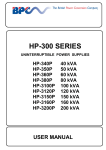
1
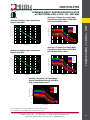
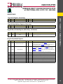
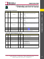
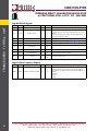
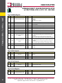
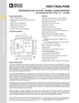
HMC1197LP7FE v00.0912 TRANCEIVERS - Tx RFICs - SMT WIDEBAND DIRECT QUADRATURE MODULATOR w/ FRACTIONAL-N PLL & VCO, 100 - 4000 MHz Typical Applications Features The HMC1197LP7FE is Ideal for: Very Low Noise Floor, -160 dBm/Hz • Multiband/Multi-standard Cellular BTS Diversity Transmitters Excellent Carrier & Sideband Suppression • Fixed Wireless or WLL High Output Power, +10.5 dBm Output P1dB • ISM Transceivers, 900 & 2400 MHz • GMSK, QPSK, QAM, SSB Modulators • Multiband Basestations & Repeaters Functional Diagram Very High Linearity, +30 dBm OIP3 High Modulation Accuracy Maximum Phase Detector Rate: 100 MHz Low Phase Noise: -110 dBc/Hz in Band Typical PLL FOM: -230 dBc/Hz Integer Mode, -227 dBc/Hz Fractional Mode < 160 fs Integrated RMS Jitter (10 kHz to 20 MHz) Differential Auxiliary LO output External LO Input Exact Frequency Mode: 0 Hz Fractional Frequency Error Programmable RF Output Phase Output Phase Synchronous Frequency Changes Output Phase Synchronization Internal LO Mute Function 48 Lead 7x7 mm QFN Package: 49 mm2 General Description The HMC1197LP7FE is a low noise, high linearity Direct Quadrature Modulator with Fractional-N PLL&VCO RFIC which is ideal for digital modulation applications from 0.1 to 4.0 GHz including; Cellular/3G, LTE/WiMAX/4G, Broadband Wireless Access & ISM circuits housed in a compact 7x7 mm (LP7) SMT QFN package, the HMC1197LP7FE RFIC requires minimal external components & provides a low cost alternative to more complicated double upconversion architectures. The RF output port is single-ended and matched to 50 Ohms with no external components. Auxiliary LO output (differential or single-ended), enables the HMC1197LP7FE to distribute identical frequency and phase signals to multiple destinations. Individual gain settings ensure optimal signal levels tailored to each output. External VCO input allows the HMC1197LP7FE to lock external VCOs, and enables cascaded LO architectures for MIMO radio applications. Two separate Charge Pump (CP) outputs enable separate loop filters optimized for both integrated and external VCOs, and seamless switching between integrated or external VCOs during operation. Programmable RF output phase feature can further phase adjust and synchronize multiple HMC1197LP7FEs enabling scalable MIMO and beam-forming radio architectures. Integrated programmable Low Pass Filter (LPF) on the modulator LO input ensures no LO harmonic contribution to modulator sideband rejection performance. Sixteen programmable LPF bands enable true wideband operation, eliminating the need for external band specific harmonic filtering hardware. Additional features include configurable LO output mute function. Exact Frequency Mode that enables the HMC1197LP7FE to generate fractional frequencies with 0 Hz frequency error and the ability to synchronously change frequencies without changing the phase of the output signal. 1 For price, delivery and to place orders: Hittite Microwave Corporation, 2 Elizabeth Drive, Chelmsford, MA 01824 Phone: 978-250-3343 Fax: 978-250-3373 Order On-line at www.hittite.com Application Support: Phone: 978-250-3343 or [email protected] HMC1197LP7FE v00.0912 WIDEBAND DIRECT QUADRATURE MODULATOR w/ FRACTIONAL-N PLL & VCO, 100 - 4000 MHz Electrical Specifications, See Test Conditions on page-4. Typ. Typ. Typ. Typ. 450-960 1700-2200 2200-2700 3400-4000 Units MHz Output Power 0.4 1.6 1.6 -0.6 dBm Conversion Voltage Gain -5.7 -4.5 -4.5 -6.7 dB Output P1dB +10.5 +10.5 +10 +10 dBm Output Noise Floor -162 -160 -158 -158 dBm/Hz Output IP3 +32 +30 +30 +22 dBm Carrier Feedthrough (uncalibrated) -45 -40 -35 -33 dBm Sideband Suppression (uncalibrated) 40 40 45 35 dBc RF Port Return Loss 12 14 15 12 dB Electrical Specifications (Continued) Parameter Conditions Min. Typ. Max. Units 4000 MHz RF Output RF Frequency Range 100 RF Return Loss 15 dB Baseband Input Port Baseband Input DC Voltage (Vbbdc) +0.45 (+0.4 to +0.5) V Single-ended. 110 pA De-embed to the lead of the device. 4.5 pF Baseband Input DC Bias Current (Ibbdc) Single-ended Baseband Input Capacitance DC Power Supply Supply Voltage (VCC1, VCC2, VCC3, VDDLS, VDDCP, BIAS, IF1P) Supply Current of +5V Supply (ICC1) +4.75 +5.0 +5.25 V Modulator ON and PLL ON 320 Modulator OFF and PLL ON 152 mA Modulator OFF and PLL OFF 12 mA Supply Voltage (V3, DVDD, RVDD, VCCPD, VCCPS, VCCHF) 3.15 +3.3 mA 3.45 V Modulator ON and PLL ON 48 mA Modulator OFF and PLL ON 48 mA Modulator OFF and PLL OFF 1 mA EN High Level Modulator disabled 5 V EN Low Level Modulator enabled 0 V 530/50 ns -75 dBm Supply Current of +3.3V Supply (ICC2) TRANCEIVERS - Tx RFICs - SMT Parameter Frequency Range, RF Enable/Disable Interface Enable/Disable Settling Time LO Leakage Isolation EN_MOD=5V, LO=2.1GHz LO Output Characteristics LO Output Frequency 50 4100 MHz VCO Frequency at PLL Input 2000 4100 MHz VCO Fundamental Frequency 2000 4100 MHz 1, 2, 4, .... 60, 62 1 62 Integer 16 524287 Fractional 20 524283 VCO Output Divider VCO Output Divider Range PLL RF Divider Characteristics 19-Bit N Divider Range For price, delivery and to place orders: Hittite Microwave Corporation, 2 Elizabeth Drive, Chelmsford, MA 01824 Phone: 978-250-3343 Fax: 978-250-3373 Order On-line at www.hittite.com Application Support: Phone: 978-250-3343 or [email protected] 2 HMC1197LP7FE v00.0912 WIDEBAND DIRECT QUADRATURE MODULATOR w/ FRACTIONAL-N PLL & VCO, 100 - 4000 MHz Electrical Specifications, (Continued) TRANCEIVERS - Tx RFICs - SMT Parameter Conditions Min. Typ. Max. Units 350 MHz Reference Input Characteristics Maximum Reference Input Frequency Phase Detector (PD) PD Frequency Fractional Mode DC 100 MHz Integer Mode DC 100 MHz Harmonics fo Mode at 4000 MHz 2nd / 3rd / 4th -30/-32/-32 dBc VCO Output Divider VCO RF Divider Range 1,2,4,6,8,...,62 1 62 Max = 219 - 1 16 524,287 Fractional nominal divide ratio varies (-3 / +4) dynamically max 20 524,283 AC Coupled 1 PLL RF Divider Characteristics 19-Bit N-Divider Range (Integer) 19-Bit N-Divider Range (Fractional) REF Input Characteristics Max Ref Input Frequency Ref Input Voltage 2 Ref Input Capacitance 14-Bit R-Divider Range 350 MHz 3.3 Vpp 5 pF 1 16,383 PD Frequency Fractional Mode DC 100 MHz PD Frequency Integer Mode DC 100 MHz Phase Detector (PD) VCO Open Loop Phase Noise at fo @ 4 GHz 10 kHz Offset -78 dBc/Hz 100 kHz Offset -108 dBc/Hz 1 MHz Offset -134.5 dBc/Hz 10 MHz Offset -156 dBc/Hz 100 MHz Offset -171 dBc/Hz 10 kHz Offset -83 dBc/Hz 100 kHz Offset -113 dBc/Hz VCO Open Loop Phase Noise at fo @ 4 GHz/2 = 2 GHz 1 MHz Offset -139.5 dBc/Hz 10 MHz Offset -165.5 dBc/Hz 100 MHz Offset -167 dBc/Hz Figure of Merit 3 Floor Integer Mode Normalized to 1 Hz -230 dBc/Hz Floor Fractional Mode Normalized to 1 Hz -227 dBc/Hz Flicker (Both Modes) Normalized to 1 Hz -268 dBc/Hz For price, delivery and to place orders: Hittite Microwave Corporation, 2 Elizabeth Drive, Chelmsford, MA 01824 Phone: 978-250-3343 Fax: 978-250-3373 Order On-line at www.hittite.com Application Support: Phone: 978-250-3343 or [email protected] HMC1197LP7FE v00.0912 WIDEBAND DIRECT QUADRATURE MODULATOR w/ FRACTIONAL-N PLL & VCO, 100 - 4000 MHz Electrical Specifications, (Continued) Conditions Min. Typ. Max. Units VCO Tuning Sensitivity at 4053 MHz Measured at 2.5 V 15 MHz/V VCO Tuning Sensitivity at 3777 MHz Measured at 2.5 V 13 MHz/V VCO Tuning Sensitivity at 3411 MHz Measured at 2.5 V 12 MHz/V VCO Tuning Sensitivity at 2943 MHz Measured at 2.5 V 11.5 MHz/V VCO Supply Pushing Measured at 2.5 V 2 MHz/V Test Conditions: Unless Otherwise Specified, the Following Test Conditions Were Used Parameter Condition Temperature +25 °C Baseband Input Frequency 200 kHz Baseband Input DC Voltage (Vbbdc) +0.45V Baseband Input AC Voltage (Peak to Peak Differential, I and Q) 1.3V Baseband Input AC Voltage for OIP3 Measurements (Peak to Peak Differential, I and Q) 650 mV per tone @ 150 & 250 KHz Baseband Input AC Voltage for Noise Floor Measurements (Peak to Peak Differential, I and Q) no baseband input voltage Frequency Offset for Output Noise Measurements 20 MHz Supply Voltage (VCC1, VCC2, VCC3, VDDLS, VDDCP, BIAS) +5.0V Supply Voltage (V3, DVDD, RVDD, VCCPD, VCCPS, VCCHF) +3.3V LO Power Level TRANCEIVERS - Tx RFICs - SMT Parameter VCO Characteristics Maximum Power Refer to HMC1197LP7FE Application Schematic Herein Mounting Configuration Sideband & Carrier Feedthrough Uncalibrated Filter Bank Selection vs. Frequency Table Frequency (MHz) ≤ 500 600 700 800 900 1000/1100 1200 1300/1400/1500 Filter Bank Selection 0 1 5 7 8 0 7 8 1600 1700/1800 1900/2000 9 10 11 2000 ≥ 15 Calibrated vs. Uncalibrated Test Results During the Uncalibrated Sideband and Carrier Suppression tests, care is taken to ensure that the I/Q signal paths from the Vector Signal Generator (VSG) to the Device Under Test (DUT) are equal. The “Uncalibrated” Sideband and Carrier Suppression plots were measured at T= -40 °C, +25 °C, and +85 °C. The “Calibrated” Sideband Suppression data was plotted after a manual adjustment of the I/Q amplitude balance and I/Q phase offset (skew) at +25 °C, 5V and 3.3V Vcc, LO maximum power level. The +25 °C adjustment settings were held constant during tests over temperature. The “Calibrated” Carrier Suppression data was plotted after a manual adjustment of the IP/IN & QP/QN DC offsets at +25 °C, 5V and 3.3V Vcc, LO maximum power level. The +25 °C adjustment settings were held constant during tests over temperature. For price, delivery and to place orders: Hittite Microwave Corporation, 2 Elizabeth Drive, Chelmsford, MA 01824 Phone: 978-250-3343 Fax: 978-250-3373 Order On-line at www.hittite.com Application Support: Phone: 978-250-3343 or [email protected] 4 HMC1197LP7FE v00.0912 WIDEBAND DIRECT QUADRATURE MODULATOR w/ FRACTIONAL-N PLL & VCO, 100 - 4000 MHz RF Output IP3, P1dB & Noise Floor @ 20 MHz Offset vs. Frequency Over Temperature OUTPUT POWER (dBm) 0 -5 -10 +25C +85C -40C -15 0 1000 2000 3000 4000 -110 30 -120 20 -130 OUTPUT IP3 10 -140 0 -150 -10 -160 +25C +85C -40C -20 SET-UP NOISE FLOOR -30 0 1000 2000 -170 -180 4000 3000 FREQUENCY (MHz) Uncalibrated Carrier Feedthrough vs. Frequency Over Temperature [1] Calibrated Carrier Feedthrough vs. Frequency Over Temperature [1] 0 0 -10 CARRIER FEEDTHROUGH (dBm) +25C +85C -40C -20 -30 -40 -50 -60 -70 +25C +85C -40C -10 -20 -30 -40 -50 -60 -70 -80 -90 0 1000 2000 3000 4000 0 1000 FREQUENCY (MHz) 2000 3000 4000 FREQUENCY (MHz) Uncalibrated Carrier Feedthrough vs. Frequency Over Temperature When Modulator is Disabled RF Return Loss vs. Frequency 0 -20 -30 -5 -40 RETURN LOSS (dB) CARRIER FEEDTHROUGH (dBm) NOISE FLOOR OUTPUT P1dB FREQUENCY (MHz) CARRIER FEEDTHROUGH (dBm) TRANCEIVERS - Tx RFICs - SMT 5 40 OUTPUT NOISE FLOOR @20 MHz (dBm/Hz) 10 OUTPUT P1dB (dBm) & OUTPUT IP3 (dBm) RF Output Power vs. Frequency Over Temperature -50 -60 -70 -80 -90 -110 0 1000 2000 3000 -15 -20 +25C +85C -40C -100 -10 -25 4000 FREQUENCY (MHz) 0 0.5 1 1.5 2 2.5 3 3.5 4 FREQUENCY (MHz) [1] See note titled “Calibrated vs. Uncalibrated test results” herein. 5 For price, delivery and to place orders: Hittite Microwave Corporation, 2 Elizabeth Drive, Chelmsford, MA 01824 Phone: 978-250-3343 Fax: 978-250-3373 Order On-line at www.hittite.com Application Support: Phone: 978-250-3343 or [email protected] HMC1197LP7FE v00.0912 WIDEBAND DIRECT QUADRATURE MODULATOR w/ FRACTIONAL-N PLL & VCO, 100 - 4000 MHz OUTPUT POWER (dBm) -30 -5 -45 SIDEBAND SUPPRESSION -10 -15 0 1000 Low (0) Medium (1) High (2) Max. (3) 2000 3000 -60 SIDEBAND SUPPRESSION (dBc) 0 -75 4000 40 -110 30 -120 20 -130 OUTPUT IP3 -140 10 NOISE FLOOR 0 -160 -10 -20 Low Medium High Max. -30 -40 0 1000 FREQUENCY (MHz) -180 SET-UP NOISE FLOOR 2000 3000 -190 4000 Calibrated Sideband Suppression vs. Frequency Over Temperature [1] 0 0 +25C +85C -40C -10 SIDEBAND SUPPRESSION (dBc) SIDEBAND SUPPRESSION (dBc) -170 (0) (1) (2) (3) FREQUENCY (MHz) Uncalibrated Sideband Suppression vs. Frequency Over Temperature [1] -20 -30 -40 -50 -60 -10 +25C +85C -40C -20 -30 -40 -50 -60 -70 -80 -90 -100 -70 0 1000 2000 3000 4000 0 1000 FREQUENCY (MHz) -45 1000 SIDEBAND SUPPRESSION 2000 3000 -60 -75 4000 FREQUENCY (MHz) OUTPUT P1dB (dBm) & OUTPUT IP3 (dBm) -30 0 4000 40 -110 30 -120 20 -130 OUTPUT IP3 -140 10 0 OUTPUT P1dB -150 NOISE FLOOR -160 -10 -30 -170 4.75V 5.00V 5.25V -20 0 1000 SET-UP NOISE FLOOR 2000 3000 -180 4000 OUTPUT NOISE FLOOR @20 MHz (dBm/Hz) 0 SIDEBAND SUPPRESSION (dBc) -15 4.75V 5.00V 5.25V 3000 RF Output IP3, P1dB & Noise Floor @ 20 MHz Offset vs. Frequency Over Supply Voltage 0 OUTPUT POWER -15 2000 FREQUENCY (MHz) RF Output Power & SBR vs. Frequency Over Supply Voltage OUTPUT POWER (dBm) -150 OUTPUT P1dB TRANCEIVERS - Tx RFICs - SMT -15 OUTPUT POWER OUTPUT NOISE FLOOR @20 MHz (dBm/Hz) 5 RF Output IP3, P1dB & Noise Floor @ 20 MHz Offset vs. Frequency Over LO Power OUTPUT P1dB (dBm) & OUTPUT IP3 (dBm) RF Output Power & SBR vs. Frequency Over LO Power FREQUENCY (MHz) [1] See note titled “Calibrated vs. Uncalibrated test results” herein. For price, delivery and to place orders: Hittite Microwave Corporation, 2 Elizabeth Drive, Chelmsford, MA 01824 Phone: 978-250-3343 Fax: 978-250-3373 Order On-line at www.hittite.com Application Support: Phone: 978-250-3343 or [email protected] 6 HMC1197LP7FE v00.0912 WIDEBAND DIRECT QUADRATURE MODULATOR w/ FRACTIONAL-N PLL & VCO, 100 - 4000 MHz RF Output Power vs. Baseband Voltage @ 2100 MHz -140 OUTPUT NOISE @20 MHz (dBm/Hz) 10 OUTPUT POWER (dBm) 9 -145 8 7 -150 6 5 -155 4 3 -160 2 0 -1 LO=930MHz LO=1930MHz LO=2530MHz LO=3530MHz -165 1 0.9 1 2 3 INPUT BASEBAND VOLTAGE (Vpp-diff) -170 -10 4 -5 0 OUTPUT POWER (dBm) 5 Normalized Baseband Frequency Response [1] BASEBAND FREQUENCY RESPONSE (dBc) TRANCEIVERS - Tx RFICs - SMT 11 RF Output Noise @ 20 MHz Offset vs. Output Power Over LO Frequency 1 0 -1 -2 -3 -4 -5 -6 -7 -8 -9 -10 -11 1 10 100 1000 IF FREQUENCY (MHz) [1] I/Q input bandwidth normalized to gain at 1 MHz (fLO=1800 MHz). I/Q inputs are matched to 100 Ohms differentially. 7 For price, delivery and to place orders: Hittite Microwave Corporation, 2 Elizabeth Drive, Chelmsford, MA 01824 Phone: 978-250-3343 Fax: 978-250-3373 Order On-line at www.hittite.com Application Support: Phone: 978-250-3343 or [email protected] HMC1197LP7FE v00.0912 WIDEBAND DIRECT QUADRATURE MODULATOR w/ FRACTIONAL-N PLL & VCO, 100 - 4000 MHz Auxiliary LO Output, Fractional Mode Closed Loop Phase Noise @3600 MHz with various divider ratios[1] Auxiliary LO Output, Open Loop Phase Noise @ 3600 MHz PHASE NOISE(dBc/Hz) PHASE NOISE(dBc/Hz) -60 -80 -100 -120 -140 Div1 Div2 Div4 Div8 Div16 Div32 Div62 -100 -120 -140 -160 -160 -180 1 10 100 1000 10000 -180 100000 1 10 100 1000 10000 Auxiliary LO Output, Fractional Mode Closed Loop Phase Noise @4100 MHz with various divider ratios[1] Auxiliary LO Output, Open Loop Phase Noise @ 4100 MHz -40 -80 Div1 Div2 Div4 Div8 Div16 Div32 Div62 PHASE NOISE(dBc/Hz) -60 PHASE NOISE(dBc/Hz) 100000 OFFSET (KHz) OFFSET (KHz) -80 -100 -120 -140 -100 -120 -140 TRANCEIVERS - Tx RFICs - SMT -80 -40 -160 -160 -180 1 10 100 1000 10000 -180 100000 1 10 OFFSET (KHz) 100 1000 10000 100000 OFFSET (KHz) Auxiliary LO Output, Fractional Mode Closed Loop Phase Noise @ 3300 MHz with various divider ratios[1] PHASE NOISE (dBc/Hz) -80 Div1 Div2 Div4 Div8 Div16 Div32 Div62 -100 -120 -140 -160 -180 1 10 100 1000 10000 100000 OFFSET (KHz) [1] Using 122.88 MHz clock input, 61.44 MHz PFD, 2.5 mA CP, 174 uA Leakage [2] Using 100 MHz clock input, 50MHz PFD, 2.5 mA CP, 174 uA Leakage For price, delivery and to place orders: Hittite Microwave Corporation, 2 Elizabeth Drive, Chelmsford, MA 01824 Phone: 978-250-3343 Fax: 978-250-3373 Order On-line at www.hittite.com Application Support: Phone: 978-250-3343 or [email protected] 8 HMC1197LP7FE v00.0912 WIDEBAND DIRECT QUADRATURE MODULATOR w/ FRACTIONAL-N PLL & VCO, 100 - 4000 MHz -40 -60 -60 PHASE NOISE(dBc/Hz) PHASE NOISE (dBc/Hz) Auxiliary LO Output, Open Loop Phase Noise vs. Frequency -40 -80 -100 -120 3862 MHz 3643 MHz 3491 MHz 3044 MHz 2558 MHz 2129 MHz -140 -160 -180 1 10 -80 -100 -120 3862.4 Mhz 3643.33 MHz 3491.74 MHz 3044 MHz 2558 MHz 2129.4 MHz -140 -160 100 1000 10000 -180 100000 1 10 Auxiliary LO Output, Open Loop Phase Noise vs. Temperature 10000 100000 -40 +25 C -40 C +85 C -120 -60 100 kHz Offset -130 PHASE NOISE(dBc/Hz) -110 1 MHz Offset -140 -150 -160 -80 -100 -120 -140 -160 -170 100 MHz Offset -180 30 -180 300 100 4000 1000 1 10 Fractional-N Spurious Performance @ 2646.96 MHz Exact Frequency Mode OFF [1] 100 1000 10000 100000 OFFSET (KHz) FREQUENCY (MHz) Figure of Merit for PLL/VCO -40 NORMALIZED PHASE NOISE (dBc/Hz) -200 -60 PHASE NOISE(dBc/Hz) 1000 Fractional-N Spurious Performance @ 2646.96 MHz Exact Frequency Mode ON [1] -100 -80 -100 -120 -140 -160 -180 100 OFFSET (KHz) OFFSET (KHz) PHASE NOISE (dBc/Hz) TRANCEIVERS - Tx RFICs - SMT Auxiliary LO Output, Open Loop Phase Noise vs. Frequency 1 10 100 1000 10000 100000 OFFSET (KHz) -210 Typ FOM vs Offset -220 FOM Floor FOM 1/f Noise -230 -240 100 1000 10 4 10 5 10 6 FREQUENY OFFSET (Hz) [1] 122.88 MHz clock input, PFD = 61.44 MHz, Channel Spacing = 240 KHz 9 For price, delivery and to place orders: Hittite Microwave Corporation, 2 Elizabeth Drive, Chelmsford, MA 01824 Phone: 978-250-3343 Fax: 978-250-3373 Order On-line at www.hittite.com Application Support: Phone: 978-250-3343 or [email protected] HMC1197LP7FE v00.0912 WIDEBAND DIRECT QUADRATURE MODULATOR w/ FRACTIONAL-N PLL & VCO, 100 - 4000 MHz Auxiliary LO Output Power vs Temperature [1] Integrated RMS Jitter [2] INTEGRATED JITTER (ps) OUTPUT POWER (dBm) 10 5 0 +85C -40C +25C -5 -10 0.25 0.2 0.15 0.1 -40 C +25 C +85 C 0.05 100 0 1000 0 500 1000 1500 2000 2500 3000 4000 Reference Input Sensitivity, Square Wave, 50 Ω [3] Typical VCO Sensitivity -220 80 ML core, Tuning Cap 15 70 -222 14 MHz sq 25 MHz sq 50 MHz sq 100 MHz sq MH core, Tuning Cap 7 60 -224 L core, Tuning Cap 15 H core, Tuning Cap 7 50 FOM (dBc/Hz) KVCO (MHz/V) 3500 OUTPUT FREQUENCY (MHz) OUTPUT FREQUENCY (MHz) CL core, Tuning Cap 15 40 CH core, Tuning Cap 15 30 -226 -228 -230 20 -232 TRANCEIVERS - Tx RFICs - SMT 0.3 15 10 0 0 1 2 3 4 -234 -12 5 -9 TUNING VOLTAGE (V) Reference Input Sensitivity, Sinusoid Wave, 50 Ω [3] -3 0 3 Phase Noise Floor FOM vs Reference Power & Frequency [4] -200 -200 -205 -205 FLOOR FOM (dBc/Hz) 14 MHz sin 100 MHz sq 50 MHz sq 25 MHz sin -210 FOM (dBc/Hz) -6 REFERENCE POWER (dBm) -215 -220 -225 -210 25 MHz -215 14 MHz -220 50 MHz -225 -230 -230 -235 -235 100 MHz -20 -15 -10 -5 0 5 -20 REFERENCE POWER (dBm) -15 -10 -5 0 5 REFERENCE POWER (dBm) [1] Both Aux. LO and MOD LO Gain Set to ‘3’ (Max Level), both Aux. LO and MOD LO Buffer Enabled, measured from Auxiliary LO Port. [2] RMS Jitter data is measured in fractional mode using 50 MHz reference frequency, from 1 kHz to 100 MHz integration bandwidth. [3] Measured from a 50 Ω source with a 100 Ω external resistor termination. See PLL with Integrated RF VCOs Operating Guide Reference Input Stage section for more details. Full FOM performance up to maximum 3.3 Vpp input voltage. [4] Measured wıth sıne wave reference ınput. For price, delivery and to place orders: Hittite Microwave Corporation, 2 Elizabeth Drive, Chelmsford, MA 01824 Phone: 978-250-3343 Fax: 978-250-3373 Order On-line at www.hittite.com Application Support: Phone: 978-250-3343 or [email protected] 10 HMC1197LP7FE v00.0912 WIDEBAND DIRECT QUADRATURE MODULATOR w/ FRACTIONAL-N PLL & VCO, 100 - 4000 MHz Forward Transmission Gain Closed Loop Phase Noıse Wıth External VCO HMC384LP4E [1] -40 PHASE NOISE(dBc/Hz) FORWARD TRANMISSION GAIN (dB) 10 5 0 -60 S21 EXT-IN LO OUT DIFFERENTIAL OUTPUT 15 -5 S21 EXT-IN LO OUT SINGLE-ENDED OUTPUT -80 -100 -120 -140 -160 400 800 1200 1600 2000 2400 -180 2800 1 10 Auxiliary LO Differential Output Return Loss -5 -5 RETURN LOSS (dB) 0 -15 -20 -25 -30 1000 10000 Auxiliary LO Single Ended Output Return Loss 0 -10 100 OFFSET (KHz) OUTPUT FREQUENCY (MHz) RETURN LOSS (dB) TRANCEIVERS - Tx RFICs - SMT 20 -10 -15 -20 -25 100 1000 OUTPUT FREQUENCY (MHz) -30 100 1000 OUTPUT FREQUENCY (MHz) [1] S21 from Ext_VCO (pin 35, 36) in and LO (pin26, 27) out. 11 For price, delivery and to place orders: Hittite Microwave Corporation, 2 Elizabeth Drive, Chelmsford, MA 01824 Phone: 978-250-3343 Fax: 978-250-3373 Order On-line at www.hittite.com Application Support: Phone: 978-250-3343 or [email protected] HMC1197LP7FE v00.0912 WIDEBAND DIRECT QUADRATURE MODULATOR w/ FRACTIONAL-N PLL & VCO, 100 - 4000 MHz VCC1, VCC2, VCC3, VDDLS, VDDCP, BIAS, IF1P, EN_MOD -0.3V to +5.5V V3, DVDD, RVDD, VCCPD, VCCPS, VCCHF -0.3V to +3.6V Baseband Input Voltage (AC + DC) (Reference to GND) -0.3V to + 1.3V Junction Temperature 150°C Thermal Resistance (Rth) (junction to ground paddle) 4.5 °C/W Storage Temperature -65 to +150 °C Operating Temperature -40 to +85 °C ESD Sensitivity (HBM) 1C ELECTROSTATIC SENSITIVE DEVICE OBSERVE HANDLING PRECAUTIONS Outline Drawing TRANCEIVERS - Tx RFICs - SMT Absolute Maximum Ratings NOTES: 1. PACKAGE BODY MATERIAL: LOW STRESS INJECTION MOLDED PLASTIC SILICA AND SILICON IMPREGNATED. 2. LEAD AND GROUND PADDLE MATERIAL: COPPER ALLOY. 3. LEAD AND GROUND PADDLE PLATING: 100% MATTE TIN. 4. DIMENSIONS ARE IN INCHES [MILLIMETERS]. 5. LEAD SPACING TOLERANCE IS NON-CUMULATIVE. 6. CHARACTERS TO BE HELVETICA MEDIUM, .025 HIGH, WHITE INK, OR LASER MARK LOCATED APPROX. AS SHOWN. 7. PAD BURR LENGTH SHALL BE 0.15mm MAX. PAD BURR HEIGHT SHALL BE 0.25mm MAX. 8. PACKAGE WARP SHALL NOT EXCEED 0.05mm 9. ALL GROUND LEADS AND GROUND PADDLE MUST BE SOLDERED TO PCB RF GROUND. 10. REFER TO HITTITE APPLICATION NOTE FOR SUGGESTED PCB LAND PATTERN. Package Information Part Number Package Body Material Lead Finish HMC1197LP7FE RoHS-compliant Low Stress Injection Molded Plastic 100% matte Sn MSL Rating MSL1 [1] Package Marking [2] H1197 XXXX [1] Max peak reflow temperature of 260 °C [2] 4-Digit lot number XXXX For price, delivery and to place orders: Hittite Microwave Corporation, 2 Elizabeth Drive, Chelmsford, MA 01824 Phone: 978-250-3343 Fax: 978-250-3373 Order On-line at www.hittite.com Application Support: Phone: 978-250-3343 or [email protected] 12 HMC1197LP7FE v00.0912 WIDEBAND DIRECT QUADRATURE MODULATOR w/ FRACTIONAL-N PLL & VCO, 100 - 4000 MHz TRANCEIVERS - Tx RFICs - SMT Pin Descriptions Pin Number Function Description 1 VDDCP Power Supply for charge pump analog section, 5.0V nominal. External bypass decoupling for precision bias circuits, 5.0V nominal. 2 BIAS 3,4 CP1,CP2 Charge Pump Outputs. 5 RVDD Reference Supply, 3.3V nominal. 6 XREFP Reference Input. DC bias is generated internally. Normally AC coupled externally. 7 DVDD DC Power Supply for Digital (CMOS) Circuitry, 3.3V nominal. 8, 13, 14, 22, 23, 24, 28, 29, 30, 41, 42 N/C The pins are not connected internally; however, all data shown herein was measured with these pins connected to RF/DC ground externally. 9 EN_MOD This pin has a 10 Kohm pulldown resistor to GND. When connected to GND or left floating the chip is fully enabled. When connected to VCC the LO amplifiers and the mixers are disabled. 10 IF1P 11, 12 QN, QP Supply voltage for the LO and mixer stage, 5.0V nominal. Q channel differential baseband input.These are high impedance ports. The nominal recommended bias voltage is 0.45V (0.4V-0.5V)[1].The nominal recommended baseband input AC voltage is 1.3V peak-to-peak differential.By adjusting the DC offsets on ports QN & QP , the Carrier Suppression of the device can be optimized for a specific frequency band and LO power level. The typical offset voltege for optimization is less than 15 mV. The amplitude and phase difference between The I and Q inputs can be adjusted in order to optimize the Sideband Suppression for a specific frequency band and LO power level 15, 16, 17, 18, 20 GND These pins and package base must be connected to RF and DC ground. 19 RFOUT DC coupled and matched to 50 Ohms. Output requires an external DC blocking capacitor. 21 VCC3 25, 26 IP, IN Supply voltage for the output stages, 5.0V nominal. I channel differential baseband input. These are high impedance ports. The nominal recommended bias voltage is 0.45V (0.4V-0.5V). The nominal recommended baseband input AC voltage is 1.3V peak-topeak differential.By adjusting the DC offsets on ports IN & IP , the Carrier Suppression of the device can be optimized for a specific frequency band and LO power level. The typical offset voltege for optimization is less than 15 mV. The amplitude and phase difference between The I and Q inputs can be adjusted in order to optimize the Sideband Suppression for a specific frequency band and LO power level 13 27 V3 Supply pin for low pass filter, 3.3V nominal. 31 CHIP_EN Chip Enable. Connect to logic high for normal operation. 32, 33 LON, LOP LO outputs. AC coupled and matched to 50 Ohms single ended. Do not need external DC decoupling capacitors. The ports could be single-ended or differential. 34 VCC1 VCO analog supply 1, 5.0V nominal. 35 VCC2 VCO analog supply 2, 5.0V nominal. 36 VTUNE VCO Varactor. Tuning Port Input. 37 SEN PLL Serial Port Enable (CMOS) Logic Input. 38 SDI PLL Serial Port Data (CMOS) Logic Input. 39 SCK PLL Serial Port Clock (CMOS) Logic Input. For price, delivery and to place orders: Hittite Microwave Corporation, 2 Elizabeth Drive, Chelmsford, MA 01824 Phone: 978-250-3343 Fax: 978-250-3373 Order On-line at www.hittite.com Application Support: Phone: 978-250-3343 or [email protected] HMC1197LP7FE v00.0912 WIDEBAND DIRECT QUADRATURE MODULATOR w/ FRACTIONAL-N PLL & VCO, 100 - 4000 MHz Pin Number Function Description 40 LD/SDO Lock Detect, or Serial Data, or General Purpose (CMOS) Logic Output (GPO). 43 EXT_N External VCO negative input. 44 EXT_P External VCO positive input. 45 VCCHF Analog supply, 3.3V nominal. 46 VCCPS Analog supply, Prescaler, 3.3V nominal. 47 VCCPD Analog supply, Phase Detector, 5.0 V nominal. 48 VDDLS Analog supply, Charge Pump, 5.0 V nominal. For price, delivery and to place orders: Hittite Microwave Corporation, 2 Elizabeth Drive, Chelmsford, MA 01824 Phone: 978-250-3343 Fax: 978-250-3373 Order On-line at www.hittite.com Application Support: Phone: 978-250-3343 or [email protected] TRANCEIVERS - Tx RFICs - SMT Pin Descriptions (continued) 14 HMC1197LP7FE v00.0912 WIDEBAND DIRECT QUADRATURE MODULATOR w/ FRACTIONAL-N PLL & VCO, 100 - 4000 MHz TRANCEIVERS - Tx RFICs - SMT Evaluation PCB The circuit board used in the application should use RF circuit design techniques. Signal lines should have 50 ohm impedance while the package ground leads and exposed paddle should be connected directly to the ground plane similar to that shown. A sufficient number of via holes should be used to connect the top and bottom ground planes. The evaluation circuit board shown is available from Hittite upon request. Evaluation PCB Schematic To view this Evaluation PCB Schematic please visit www.hittite.com and choose HMC1197LP7FE from the “Search by Part Number” pull down menu to view the product splash page. Evaluation Order Information Item 15 Contents Part Number Evaluation PCB Only HMC1197LP7FE Evaluation PCB EVAL01-HMC1197LP7F Evaluation Kit HMC1197LP7FE Evaluation PCB USB Interface Board 6’ USB A Male to USB B Female Cable CD ROM (Contains User Manual, Evaluation PCB Schematic, Evaluation Software, Hittite PLL Design Software) EKIT01-HMC1197LP7F For price, delivery and to place orders: Hittite Microwave Corporation, 2 Elizabeth Drive, Chelmsford, MA 01824 Phone: 978-250-3343 Fax: 978-250-3373 Order On-line at www.hittite.com Application Support: Phone: 978-250-3343 or [email protected] HMC1197LP7FE v00.0912 WIDEBAND DIRECT QUADRATURE MODULATOR w/ FRACTIONAL-N PLL & VCO, 100 - 4000 MHz Reg 00h ID Register (Read Only) BIT TYPE NAME W DEFLT [23:0] RO Chip ID 24 C1201h DESCRIPTION Chip ID Number Reg 00h Read Address Register (Write Only) BIT TYPE NAME W DEFLT [4:0] WO Read Address 5 - DESCRIPTION Specifies the address to be read in the next read cycle. Reg 00h Reset Strobe Register (Write Only) (Continued) BIT TYPE NAME W DEFLT [5] WO Reset 1 - W DEFLT DESCRIPTION Strobe (WRITE ONLY) generates soft reset. Resets all digital and registers to default states Reg 01h Chip Enable Register BIT [0] TYPE R/W NAME Chip Enable Pin Select 1 DESCRIPTION 1 1 = Chip enable via CHIP_EN pin, Reg 01h[0]=1 and CHIP_EN pin low places the PLL in Power Down Mode 0 = Chip enable via SPI - Reg 01h[0] = 0, CHIP_EN pin ignored (see Power Down Mode description for more details) Controls Chip Enable (Power Down) if Reg 01h[0] =0 Reg 01h[0]=0 and Reg 01h[1]=1 - chip is enabled, CHIP_EN pin don’t care Reg 01h[0]=0 and Reg 01h[1]=0 - chip disabled, CHIP_EN pin don’t care (see Power Down Mode description for more information) [1] R/W SPI Chip Enable 1 1 [2] R/W Keep Bias On 1 0 keeps internal bias generators on, ignores Chip enable control [3] R/W Keep PFD Pn 1 0 keeps PFD circuit on, ignores Chip enable control keeps Charge Pump on, ignores Chip enable control [4] R/W Keep CP On 1 0 [5] R/W Keep Reference Buffer ON 1 0 keeps Reference buffer block on, ignores Chip enable control [6] R/W Keep VCO on 1 0 keeps VCO divider buffer on, ignores Chip enable control [7] R/W Keep GPO Driver ON 1 0 keeps GPO output Driver ON, ignores Chip enable control [9:8] R/W reserved 2 0 reserved For price, delivery and to place orders: Hittite Microwave Corporation, 2 Elizabeth Drive, Chelmsford, MA 01824 Phone: 978-250-3343 Fax: 978-250-3373 Order On-line at www.hittite.com Application Support: Phone: 978-250-3343 or [email protected] TRANCEIVERS - Tx RFICs - SMT REGISTER MAP 16 HMC1197LP7FE v00.0912 WIDEBAND DIRECT QUADRATURE MODULATOR w/ FRACTIONAL-N PLL & VCO, 100 - 4000 MHz TRANCEIVERS - Tx RFICs - SMT Reg 02h Reference Divider Register BIT TYPE NAME W DEFLT [13:0] R/W R Divider Setting 14 1 DESCRIPTION Reference Divider ’R’ Value (EQ 8) min 0d max 16383d Reg 03h Frequency Register - Integer Part BIT TYPE NAME W DEFLT DESCRIPTION Divider Integer part, used in all modes, see (EQ 10) [18:0] R/W Integer Setting 19 25d 19h Fractional Mode min 20d max 219 -4 = 7FFFCh = 524,284d Integer Mode min 16d max 219-1 = 7FFFFh = 524,287d Reg 04h Frequency Register - Fractional Part BIT [23:0] TYPE R/W NAME Fractional Setting W 24 DEFLT DESCRIPTION Divider Fractional part (24 bit unsigned) see Fractional Frequency Tuning Fractional Division Value = Reg4[23:0]/2^24 Used in Fractional Mode only min 0d max 2^24-1 = FFFFFFh = 16,777,215d 0 Reg 05h Reserved 17 BIT TYPE NAME W DEFLT [23:0] R/W Reserved 24 0 DESCRIPTION Reserved For price, delivery and to place orders: Hittite Microwave Corporation, 2 Elizabeth Drive, Chelmsford, MA 01824 Phone: 978-250-3343 Fax: 978-250-3373 Order On-line at www.hittite.com Application Support: Phone: 978-250-3343 or [email protected] HMC1197LP7FE v00.0912 WIDEBAND DIRECT QUADRATURE MODULATOR w/ FRACTIONAL-N PLL & VCO, 100 - 4000 MHz Reg 06h Delta Sigma Modulator Register TYPE NAME W DEFLT R/W Reserved 2 2d Reserved, Program to 0h 2d Select the Delta Sigma Modulator Type 0: 1st order 1: 2nd Order 2: 3rd Order - Recommended 3: Reserved [3:2] R/W DSM Order 2 DESCRIPTION 0: Normal SPI Load - all register load on rising edge of SEN 1: Synchronous SPI - registers Reg 03h, Reg 04h , Reg 1Ah wait to load synchronously on the next internal clock cycle. Normally (When this bit is 0) SPI writes into the internal state machines/counters happen asynchronously relative to the internal clocks. This can create freq/phase disturbances if writing register 3, 4 or 1A. When this bit is enabled, the internal SPI registers are loaded synchronously with the internal clock. This means that the data in the SPI shifter should be held constant for at least 2 PFD clock periods after SEN is asserted to allow this retiming to happen cleanly. [4] R/W Synchronous SPI Mode 1 0 [5] R/W Exact Frequency Mode Enable 1 0 [6] R/W Reserved 1 0 Reserved 1: Exact Frequency Mode Enabled 0: Exact Frequency Mode Disabled [7] R/W Fractional Bypass 1 0 0: Use Modulator, Required for Fractional Mode, 1: Bypass Modulator, Required for Integer Mode Note: When enabled fractional modulator output is ignored, but fractional modulator continues to be clocked if Reg 06h[11] =1. This feature can be used to test the isolation of the digital fractional modulator from the VCO output in integer mode. [8] R/W Autoseed EN 1 1 1: loads the modulator seed (start phase) whenever the fractional register (Reg 04h) is written 0: when fractional register (Reg 04h) write changes frequency, modulator starts at previous value (phase) [10:9] R/W Reserved 2 3d Reserved [11] R/W Delta Sigma Modulator Enable 1 1 0: Disable DSM, used for Integer Mode 1: Enable DSM Core, required for Fractional Mode [22:12] R/W Reserved 11 97d 61h TRANCEIVERS - Tx RFICs - SMT BIT [1:0] Reserved, Program to 30h For price, delivery and to place orders: Hittite Microwave Corporation, 2 Elizabeth Drive, Chelmsford, MA 01824 Phone: 978-250-3343 Fax: 978-250-3373 Order On-line at www.hittite.com Application Support: Phone: 978-250-3343 or [email protected] 18 HMC1197LP7FE v00.0912 WIDEBAND DIRECT QUADRATURE MODULATOR w/ FRACTIONAL-N PLL & VCO, 100 - 4000 MHz Reg 07h Lock Detect Configuration Register TRANCEIVERS - Tx RFICs - SMT BIT TYPE NAME W DEFLT [2:0] R/W Lock Detect Window Count Max 3 4d [13:3] R/W Reserved 11 265d 109h DESCRIPTION Lock Detect window sets the number of consecutive counts of divided VCO that must land inside the Lock Detect Window to declare LOCK 0: 5 1: 32 2: 96 3: 256 4: 512 5: 2048 6: 8192 7: 65535 Reserved, Program to 108h [11] R/W Lock Detect Enable 1 0 1: Enable Lock Detect [13:12] R/W Reserved 2 0 Reserved, Program to [14] R/W LD Mode 1 1 1: Fixed to lock detect training Mode [15] R/W CSP Enable 1 0 Cycle Slip Prevention enable. When enabled, if the phase error becomes larger than approx 70% of the PFD period, the charge-pump gain is increased by approx 6mA for the duration of the cycle.. [19:16] R/W Reserved 4 0 Reserved [20] R/W Lock Detect Training 1 0 0 to 1 transition triggers the training. Lock Detect Training is only required after changing Phase Detector frequency. After changing PD frequency a toggle Reg 07h[20] from 0 to 1 retrains the Lock Detect. [21] R/W Reserved 1 1 Reserved Reg 08h Analog Enable Register 19 BIT TYPE NAME W DEFLT DESCRIPTION [20:0] R/W Reserved 21 114687d 1BFFFh [21] R/W Hi Frequency Reference 1 0 Program 1 for XTAL > 200 MHz (sets low gain mode for high frequency crystal buffer), 0 otherwise. [22] R/W SDO Output Level 1 0 Output Logic Level on LD/SDO pin 0: 1.8 V Logic Levels 1: DVDD3V Logic Level [23] R/W Reserved 1 0 Reserved Reserved For price, delivery and to place orders: Hittite Microwave Corporation, 2 Elizabeth Drive, Chelmsford, MA 01824 Phone: 978-250-3343 Fax: 978-250-3373 Order On-line at www.hittite.com Application Support: Phone: 978-250-3343 or [email protected] HMC1197LP7FE v00.0912 WIDEBAND DIRECT QUADRATURE MODULATOR w/ FRACTIONAL-N PLL & VCO, 100 - 4000 MHz Reg 09h Charge Pump Register [6:0] [13:7] [20:14] TYPE R/W R/W R/W NAME CP DN Gain CP UP Gain Offset Current W 7 7 7 DEFLT DESCRIPTION 100d 64h Charge Pump DN Gain Control 20uA/step Affects fractional phase noise and lock detect settings 0d = 0uA 1d = 20uA 2d = 40uA ... 127d = 2.54mA 100d 64h Charge Pump UP Gain Control 20uA/step Affects fractional phase noise and lock detect settings 0d = 0uA 1d = 20uA 2d = 40uA ... 127d = 2.54mA 81d 51h Charge Pump Offset Control 5uA/step Affects fractional phase noise and spursand lock detect settings 0d = 0uA 1d = 5uA 2d = 110uA ... 127d = 635uA [21] R/W Offset Current UP 1 0 1 - Sets Direction of Reg 09h[20:14] Up, 0- UP Offset Off [22] R/W Offset Current DN 1 1 1 - Sets Direction of Reg 09h[20:14] Down, 0- DN Offset Off [23] R/W HiK charge pump Mode 1 0 Hi Kcp Charge Pump - Very Low Noise, Narrow Compliance range, requires external OpAmp in the loop filter. TRANCEIVERS - Tx RFICs - SMT BIT Reg 0Ah VCO AutoCal Configuration Register BIT TYPE NAME W DEFLT DESCRIPTION [2:0] R/W Vtune Resolution 3 6d 1,2,4,8,...,32,64,128,256 Rdiv cycles for frequency measurement. Measurement should last > 4 µsec. Note: 1 does not work if R divider = 1. [10:3] R/W Reserved 8 8d Reserved [11] R/W AutoTune Disable 1 0 1 - Disable AutoTune procedure [12] R/W Reserved 1 0 Reserved [14:13] R/W FSM Clock Select 2 1 Set the AutoCal FSM (50 MHz maximum) 0: Input Crystal Reference 1: Input Crystal Reference/4 2: Input Crystal Reference/16 3: Input Crystal Reference/32 [16:15] R/W Reserved 2 0 Reserved [17] R/W Auto Relock - One Try 1 0 1: Attempts to relock if Lock Detect fails for any reason. Only tries once. For price, delivery and to place orders: Hittite Microwave Corporation, 2 Elizabeth Drive, Chelmsford, MA 01824 Phone: 978-250-3343 Fax: 978-250-3373 Order On-line at www.hittite.com Application Support: Phone: 978-250-3343 or [email protected] 20 HMC1197LP7FE v00.0912 WIDEBAND DIRECT QUADRATURE MODULATOR w/ FRACTIONAL-N PLL & VCO, 100 - 4000 MHz TRANCEIVERS - Tx RFICs - SMT Reg 0Bh PD/CP Register 21 BIT TYPE NAME W DEFLT DESCRIPTION [3:0] R/W Reserved 4 1 Reserved PD Phase Select 1 0 Inverts the PD polarity (program to 0) 0- Use with a positive tuning slope VCO and Passive Loop Filter (default) 1- Use with a Negative Slope VCO or with an inverting Active Loop Filter with a Positive Slope VCO R/W PD Up Output Enable 1 1 Enables the PD UP output, see also Reg 0Bh Reg 7h[9] R/W PD Down Output Enable 1 0 Enables the PD DN output, see alsoReg 0Bh Reg 7h [10] R/W Reserved 2 0 Reserved, Program to 0d. [4] R/W [5] [6] [8:7] [9] R/W Force CP UP 1 0 Forces CP UP output on if CP is not forced down - Use for Test only [10] R/W Force CP DN 1 0 Forces CP DN output on if CP is not forced up - Use for Test only [11] R/W Force CP MId Rail 1 0 Force CP MId Rail - Use for Test only (if Force CP UP or Force CP DN are enabled they have precedence) [23:12] R/W Reserved 12 124d 7Ch W DEFLT Reserved. Program to 78h Reg 0Ch Exact Frequency Register BIT [23:0] TYPE R/W NAME Number of Channels per Fpd 24 0 DESCRIPTION Comparison Frequency divided by the correction rate. Must be an integer. Frequencies at exactly the correction rate will have zero frequency error. Only works in modulator Mode B. Must be 0 otherwise 0: Disabled 1: Invalid ≥ 2 valid For price, delivery and to place orders: Hittite Microwave Corporation, 2 Elizabeth Drive, Chelmsford, MA 01824 Phone: 978-250-3343 Fax: 978-250-3373 Order On-line at www.hittite.com Application Support: Phone: 978-250-3343 or [email protected] HMC1197LP7FE v00.0912 WIDEBAND DIRECT QUADRATURE MODULATOR w/ FRACTIONAL-N PLL & VCO, 100 - 4000 MHz Reg 0Fh GPO Register TYPE NAME W DEFLT DESCRIPTION Select signal to be output to SDO pin when enabled 0: Data from Reg0F[5] 1: Lock Detect Output 2. Lock Detect Trigger 3: Lock Detect Window Output 4: Ring Osc Test 5. Pullup Hard from CSP 6. PullDN hard from CSP 7. Reserved 8: Reference Buffer Output 9: Ref Divider Output 10: VCO divider Output 11. Modulator Clock from VCO divider 12. Auxiliary Clock 13. Aux SPI Clock 14. Aux SPI Enable 15. Aux SPI Data Out 16. PD DN 17. PD UP 18. SD3 Clock Delay 19. SD3 Core Clock 20. AutoStrobe Integer Write 21. Autostrobe Frac Write 22. Autostrobe Aux SPI 23. SPI Latch Enable 24. VCO Divider Sync Reset 25. Seed Load Strobe 26.-29 Not Used 30. SPI Output Buffer En 31. Soft RSTB [4:0] R/W GPO 5 1 [5] R/W GPO Test Data 1 0 1 - GPO Test Data when GPO_Select = 0 [6] R/W Prevent Automux SDO 1 0 1- Outputs GPO data only 0- Automuxes between SDO and GPO data [7] R/W LDO Driver Always On 1 0 Only for HMC SPI mode 1- LD_SDO Pin driver always on 0- LD_SDO Pin driver only on during SPI read cycle [8] R/W Disable PFET 1 0 Program to 1 if external pull-ups are used on the SDO line (Prevents conflicts on the SPI bus) [9] R/W Disable NFET 1 0 Program to 1 if external pull-downs are used on the SDO line (Prevents conflicts on the SPI bus) TRANCEIVERS - Tx RFICs - SMT BIT Reg 10h Tuning Register (Read Only) BIT TYPE NAME W DEFLT [7:0] R VCO Tune Curve 8 16d 10h [8] R VCO Tuning Busy 1 0 DESCRIPTION VCO sub-band selection. 0- maximum frequency ‘1111 1111’b- minimum frequency Indicates if the VCO tuning is in process 1- Busy 0- Not Busy For price, delivery and to place orders: Hittite Microwave Corporation, 2 Elizabeth Drive, Chelmsford, MA 01824 Phone: 978-250-3343 Fax: 978-250-3373 Order On-line at www.hittite.com Application Support: Phone: 978-250-3343 or [email protected] 22 HMC1197LP7FE v00.0912 WIDEBAND DIRECT QUADRATURE MODULATOR w/ FRACTIONAL-N PLL & VCO, 100 - 4000 MHz Reg 11h SAR Register (Read Only) TRANCEIVERS - Tx RFICs - SMT BIT NAME W DEFLT [18:0] R SAR Error Magnitude Count 19 219 - 1d 7FFFFh [19] R SAR Error Sign 1 0 DESCRIPTION SAR Error Magnitude Count SAR Error Sign 0: positive 1: negative Reg 12h GPO/LD Register (Read Only) BIT TYPE NAME W DEFLT [0] R GPO Out 1 0 GPO Output [1] R Lock Detect Out 1 0 Lock Detect Output 3 28d 1Ch W DEFLT 16 4697d 1259h W DEFLT [4:2] R Reserved DESCRIPTION Reserved Reg 13h BIST Register (Read Only) BIT [16:0] TYPE R NAME Reserved DESCRIPTION Reserved Reg 14h Auxiliary SPI Register BIT TYPE NAME DESCRIPTION [0] R/W Aux SPI Mode 1 0 1- Use the 3 outputs as an SPI port 0- Use the 3 outputs as a static GPO port [3:1] R/W Aux GPO Values 3 0 Output values when Reg 7h[1] = 1 [4] R/W Aux GPO 3.3 V 1 0 0- 1.8 V output out of the Auxiliary GPO pins when Reg 10h[1] = 1 1- 3.3 V output out of the Auxiliary GPO pins when [1] = 1 [8:5] R/W Reserved 4 1 Reserved 1 When set, CHIP_EN pin is used as a trigger for phase synchronization. Can be used to synchronize multiple HMC1197LP7FE, or to along with the Reg 20h value to phase step the output. (Exact Frequency Mode must be enabled) 0 Option to send GPO multiplexed data (ex Lock Detect) to one of the auxiliary outputs 0- None 1 - to [0] 2 - to [1] 3 - to [2] 0 When disabled: 0 - Outputs Hi Z 2 - Outputs stay driven 3 - Outputs driven to high 4 - Outputs driven to low [9] [11:10] [13:12] 23 TYPE R/W R/W R/W Phase Sync Aux SPI GPO Output Aux SPI Outputs 1 2 2 For price, delivery and to place orders: Hittite Microwave Corporation, 2 Elizabeth Drive, Chelmsford, MA 01824 Phone: 978-250-3343 Fax: 978-250-3373 Order On-line at www.hittite.com Application Support: Phone: 978-250-3343 or [email protected] HMC1197LP7FE v00.0912 WIDEBAND DIRECT QUADRATURE MODULATOR w/ FRACTIONAL-N PLL & VCO, 100 - 4000 MHz Reg 15h Manual VCO Config Register TYPE NAME W DEFLT DESCRIPTION [0] R/W Manual Calibration Mode 1 0 [5:1] R/W Capacitor Switch Setting 5 16d 10h capacitor switch setting [8:6] R/W Manual VCO Selection 3 2d Manual VCO Selection [9] R/W Manual VCO Tune Enable 1 0 1- Manual VCO tuning enabled 0- Manual VCO tuning disabled [15:10] R/W Reserved 6 18d 12h [16] R/W Enable Auto-Scale CP current 1 1 1 - Automatically scale CP current based on VCO frequency and capacitor setting 0- Don’t scale CP current [19:17] R/W Reserved 3 7d Reserved W DEFLT 1- VCO subsystem manual calibration enabled 0- VCO subsystem manual calibration disabled Reserved Reg 16h Gain Divider Register BIT [5:0] TYPE R/W NAME RF Divide Ratio 6 DESCRIPTION 1d 0 - Mute, VCO and PLL buffer On, RF output stages Off 1 - Fo 2 - Fo/2 3 - invalid, defaults to 2 4 - Fo/2 5 - invalid, defaults to 4 6 - Fo/6 ... 60 - Fo/60 61 - invalid, defaults to 60 62 - Fo/62 > 62 - invalid, defaults to 62 [7:6] R/W LO Output Buffer Gain Control 2 3d 3 - Max Gain 2 - Max Gain - 3 dB 1 - Max Gain - 6 dB 0 - Max Gain - 9 dB [9:8] R/W LO2 Output Buffer gain Control 2 2d 3 - Max Gain 2 - Max Gain - 3 dB 1 - Max Gain - 6 dB 0 - Max Gain - 9 dB [10] R/W Divider Output Stage Gain Control 1 1 1 - Max Gain 0 - Max Gain - 3 dB For price, delivery and to place orders: Hittite Microwave Corporation, 2 Elizabeth Drive, Chelmsford, MA 01824 Phone: 978-250-3343 Fax: 978-250-3373 Order On-line at www.hittite.com Application Support: Phone: 978-250-3343 or [email protected] TRANCEIVERS - Tx RFICs - SMT BIT 24 HMC1197LP7FE v00.0912 WIDEBAND DIRECT QUADRATURE MODULATOR w/ FRACTIONAL-N PLL & VCO, 100 - 4000 MHz TRANCEIVERS - Tx RFICs - SMT Reg 17h Modes Register BIT TYPE NAME W DEFLT DESCRIPTION [0] R/W VCO SubSys Master Enable 1 1 [1] R/W VCO Enable 1 1 [2] R/W External VCO Buffer Enable 1 0 External VCO Buffer to output stage enable. Only used when locking an external VCO. [3] R/W PLL Buffer Enable 1 1 PLL Buffer Enable. Used when using an internal VCO. Master enable for the entire VCO Subsystem 1 - Enable 0 - Disable Chip Enable is also required. [4] R/W LO Output Buffer Enable 1 0 Enables LO (LO_P & LO_N pins) output buffer. [5] R/W LO2 Output Buffer Enable 1 1 Enables the second (LO2_N & LO2_P pins) output buffer [6] R/W External Input Enable 1 0 Enables External VCO input [7] R/W Pre Lock Mute Enable 1 1 Mute both output buffers until the PLL is locked R/W LO Output Single-Ended Enable 1 Enables Single-Ended output mode for LO output 1- Single-ended mode, LO_N pin is enabled, and LO_P pin is disabled 0- Differential mode, both LO_N and LO_P pins enabled Please note that single-ended output is only available on LO_N pin. [8] 1 [9] R/W LO2 Output Single-Ended Enable 1 0 Enables Single-Ended output mode for LO2 output 1- Single-ended mode, LO2_N pin is enabled, and LO2_P pin is disabled 0- Differential mode, both LO2_N and LO2_P pins enabled Please note that single-ended output is only available on LO2_N pin. [10] R/W Reserved 1 0 Reserved [11] R/W Charge Pump Output Select 1 0 Connects CP to CP1 or CP2 output. 0: CP1 1: CP2 Reg 18h Bias Register BIT TYPE NAME W DEFLT DESCRIPTION [18:0] R/W Reserved 19 21697d 54C1h [19] R/W External Input buffer BIAS bit0 1 0 External Input buffer BIAS bit0 [20] R/W External Input buffer BIAS bit1 1 0 External Input buffer BIAS bit1 W DEFLT 2 2730d AAAh Reserved Reg 19h Cals Register BIT [23:0] TYPE R/W NAME Reserved DESCRIPTION Reserved. Program to 2F3h. Reg 1Ah Seed Register BIT [23:0] 25 TYPE R/W NAME Delta Sigma Modulator Seed W DEFLT 24 816897d C7701h DESCRIPTION For price, delivery and to place orders: Hittite Microwave Corporation, 2 Elizabeth Drive, Chelmsford, MA 01824 Phone: 978-250-3343 Fax: 978-250-3373 Order On-line at www.hittite.com Application Support: Phone: 978-250-3343 or [email protected] HMC1197LP7FE v00.0912 WIDEBAND DIRECT QUADRATURE MODULATOR w/ FRACTIONAL-N PLL & VCO, 100 - 4000 MHz Chip ID = 6h, Regaddress = 01h, (Reg01h) (Write Only)[1] BIT TYPE NAME W [15:0] W Harmonic LPF Band select 16 [23:16] W Reserved 8 DEFLT 15d Fh DESCRIPTION Low Pass Filter 3 dB bandwidth setting on the output of LO pins (LO_N & LO_P pins) 0: 970 MHz 1: 1000 MHz 2: 1030 MHz 3: 1055 MHzl 4: 1085 MHz 5: 1120 MHz 6: 1155 MHz 7: 1195 MHz 8: 2335 MHz 9: 2430 MHz 10: 2530 MHz 11: 2655 MHz 12: 2770 MHz 13: 2940 MHz 14: 3145 MHz 15: 3400 MHz Reserved A write of C1h is required every time bandwidth setting in Reg 21h [15:0] is changed. TRANCEIVERS - Tx RFICs - SMT Reg 21h Programmable Harmonic LPF Register [1] To write to this register initially set Reg14h[0] = 1 to forward SPI data on AuxSPI port, then write to this register with Chip_ID = 6h, and RegAddress = 1h, Then to not change the band select on teh following Register writes, write Reg14h[0] = 0h For price, delivery and to place orders: Hittite Microwave Corporation, 2 Elizabeth Drive, Chelmsford, MA 01824 Phone: 978-250-3343 Fax: 978-250-3373 Order On-line at www.hittite.com Application Support: Phone: 978-250-3343 or [email protected] 26 HMC1197LP7FE v00.0912 WIDEBAND DIRECT QUADRATURE MODULATOR w/ FRACTIONAL-N PLL & VCO, 100 - 4000 MHz Application Information TRANCEIVERS - Tx RFICs - SMT Principle of Operation Figure 1. The HMC1197LP7FE Simplified Block Diagram The HMC1197LP7FE is a low-noise, high-linearity, Direct Quadrature Modulator with Fractional-N PLL&VCO RFIC designed for directly converting complex modulated baseband signals from zero IF or low IF to RF transmission levels from 100 MHz to 4 GHz. The HMC1197LP7FE’s excellent noise and linearity performance makes it suitable for a wide range of transmission standards, including single and multicarrier CDMA, UMTS, CDMA2000, GSM/EDGE, W-CDMA, TD-SCDMA, and WiMAX/LTE applications. As shown in the simplified block diagram (Figure 1) the HMC1197LP7FE offers an easy-to-use, complete direct conversion solution in a highly compact 7 x 7 mm plastic package thereby reducing cost, area, and power consumption. The HMC1197LP7FE modulator consists of the following functional blocks: 1. PLL & VCO 2. I/Q modulator: I and Q input differential voltage-to-current converters, I and Q upconverting mixers and the differential-to-single-ended converter, high Accuracy LO quadrature phase splitter and LO limiting amplifiers 3. Harmonic Low Pass Filter I/Q Modulator The differential baseband inputs (QP, QN, IP, and IN) present a high impedance. The DC common-mode voltage at the baseband inputs sets the currents in the I and Q double-balanced mixers. The nominal baseband input DC common-mode voltage used in the characterization of the HMC1197LP7FE is 0.45V, which should be externally applied. The baseband input DC common-mode voltage can be varied between 0.4V and 0.5V to optimize overall modulator performance. It is not recommended to leave the baseband inputs floating which generates excessive current flow that may cause damage to the IC. The baseband inputs should be pulled down to GND in shutdown mode. The nominal baseband input AC Voltage used in the characterization of the HMC1197LP7FE is 1.3Vpp differential. The baseband input AC voltage can be varied to optimize overall modulator performance. It is recommended to drive the baseband inputs differentially to reduce even-order distortion products and also use reconstruction filters at the baseband inputs to avoid aliasing 27 For price, delivery and to place orders: Hittite Microwave Corporation, 2 Elizabeth Drive, Chelmsford, MA 01824 Phone: 978-250-3343 Fax: 978-250-3373 Order On-line at www.hittite.com Application Support: Phone: 978-250-3343 or [email protected] HMC1197LP7FE v00.0912 I/Q modulator includes a LO quadrature phase splitter that generates two carrier signals in quadrature followed by LO limiting amplifiers which are used to drive the I and Q mixers with saturated signal levels. Therefore, the LO path is immune to large variations in the LO input signal level and the modulator performance does not vary much with LO input power. After upconversion, the outputs of the I and Q mixers are summed together differentially and converted to singleended RF output. The single-ended RF output port is internally matched to 50 Ohms and does not require any external matching components. Only a standard DC-blocking capacitor is required at this interface. Harmonic Low Pass Filter High LO harmonic content causes amplitude and phase mismatches and ultimately performance degradation in modulator sideband rejection. hmc701 Sweeper Plot 11:18:12 AM 3/19/2012 MODULATOR SIDEBAND REJECTION (dBc) 0 -10 Targeted minimum LO harmonic level -20 Targeted maximum modulator sideband rejection -30 -40 3rd LO Harmonic -50 -60 2nd LO Harmonic -70 -80 -80 -70 -60 -50 -40 -30 -20 -10 0 LO HARMONIC LEVEL (dBc) Figure 2. Typical impact of 2nd and 3rd LO harmonic on sideband rejection. TRANCEIVERS - Tx RFICs - SMT WIDEBAND DIRECT QUADRATURE MODULATOR w/ FRACTIONAL-N PLL & VCO, 100 - 4000 MHz As shown in Figure 2, in a typical modulator with 1xLO input both the 2nd and 3rd LO harmonics affect the modulator sideband rejection performance at levels > -20 dBc relative to the LO signal power. It also shows that the 3rd LO harmonic has greater impact on modulator sideband rejection performance than the 2nd, and that there is little effect of the 2nd LO harmonic on modulator sideband rejection once the 2nd LO harmonic is below -20 dBc levels, relative to the LO signal level. Figure 3 shows the typical insertion loss of the low pass filter. 0 High Bands INSERTION LOSS (dB) -5 Band 8 -10 -15 Band 0 -20 -25 Low Bands Band 15 -30 Band 7 -35 -40 0 1000 2000 3000 4000 5000 6000 FREQUENCY (MHz) 7000 8000 9000 Figure 3. Insertion loss of the low pass filter. For price, delivery and to place orders: Hittite Microwave Corporation, 2 Elizabeth Drive, Chelmsford, MA 01824 Phone: 978-250-3343 Fax: 978-250-3373 Order On-line at www.hittite.com Application Support: Phone: 978-250-3343 or [email protected] 28 HMC1197LP7FE v00.0912 WIDEBAND DIRECT QUADRATURE MODULATOR w/ FRACTIONAL-N PLL & VCO, 100 - 4000 MHz LO harmonic filter’s 16 user programmable bands enable the user to optimally attenuate 2nd and/or 3rd LO harmonics in order to maximize sideband rejection performance. Frequency (MHz) ≤500 600 700 800 900/1000 1100 1200 1300 1400 1500 1600 1700 ≥1800 Filter Bank Selection 0 1 4 6 7 8 9 11 12 13 13 14 15 Table 2. The frequency band selection for optimal 2nd harmonic attenuation. Frequency (MHz) Filter Bank Selection ≤700 800/900 1000 1100 1200/1300/1400 1500/1600/1700 1800 1900 2000 2100 2200/2300 2400/2500/2600 ≥2700 0 1 4 5 7 8 9 10 11 12 13 14 15 Uncalibrated sideband rejection can be further improved by empirically selecting the filter bank that provides the highest rejection for a given frequency . See Table 3 and Figure 4. Table 3. Empirical filter band selection. Frequency (MHz) ≤500 600 700 800 900 1000/1100 1200 Filter Bank Selection 0 1 5 7 8 0 7 UNCALIBRATED SIDEBAND SUPPRESSION (dBc) TRANCEIVERS - Tx RFICs - SMT Table 1. The frequency band selection for optimal 3rd harmonic attenuation. 1300/1400/1500 1600 1700/1800 1900/2000 8 9 10 11 >2000 15 0 -10 3rd Harmonic Suppression 2nd Harmonic Suppression Empirical Band Selection -20 -30 -40 -50 -60 -70 0 1000 2000 3000 4000 FREQUENCY (MHz) Figure 4. Sideband suppression vs. frequency for different filter band selections. The filter bank selection process for optimal sideband rejection performance also depends on the LO power level at the output of the PLL/VCO. LO power in this example set to maximum power level. 29 For price, delivery and to place orders: Hittite Microwave Corporation, 2 Elizabeth Drive, Chelmsford, MA 01824 Phone: 978-250-3343 Fax: 978-250-3373 Order On-line at www.hittite.com Application Support: Phone: 978-250-3343 or [email protected] HMC1197LP7FE v00.0912 WIDEBAND DIRECT QUADRATURE MODULATOR w/ FRACTIONAL-N PLL & VCO, 100 - 4000 MHz Carrier feedthrough is related to the DC offsets at the differential baseband inputs of the modulator. If exactly the same DC common-mode voltage is applied to each of the baseband inputs, and there were no DC offsets at the differential baseband inputs, the LO leakage at the RF output would be perfectly suppressed. By adding small DC offset voltages at the differential baseband inputs, the carrier feedthrough can be optimized for a specific frequency band and LO power level. The carrier feedthrough can not be calibrated by the DC commonmode level at the I and Q baseband inputs. DC offsets at the differential I and Q baseband inputs should be iteratively adjusted until a minimum carrier feedthrough level is obtained. Externally available offset voltage step resolution and the modulator’s noise floor limit the minimum achievable calibrated carrier feedthrough level. The typical offset voltages for optimization are less than 15mV. Figure 5 illustrates the typical calibrated carrier feedthrough performance of the HMC1197LP7FE. In this characterization of the HMC1197LP7FE, carrier feedthrough was calibrated with 500MHz LO frequency steps at 25C and external offset voltage settings were held constant during tests over temperature. CARRIER FEEDTHROUGH (dBm) 0 +25C +85C -40C -10 -20 -30 -40 -50 -60 -70 -80 -90 0 1000 2000 3000 4000 TRANCEIVERS - Tx RFICs - SMT Carrier Feedthrough Calibration FREQUENCY (MHz) Figure 5. The HMC1197LP7FE Calibrated Carrier Feedthrough Sideband Suppression Calibration Sideband suppression is related to relative gain and relative phase offsets between the I-channel and Q-channel. The amplitude and phase difference between the I and Q inputs can be adjusted in order to optimize the sideband suppression for a specific frequency band and LO power level. The amplitude and phase offsets at the I and Q inputs should be iteratively adjusted until a minimum sideband suppression level is obtained. The externally available amplitude and phase steps and the modulator’s noise floor limit the minimum achievable calibrated sideband suppression level. Figure 6 illustrates the typical calibrated sideband suppression performance of the HMC1197LP7FE. In this characterization of the HMC1197LP7FE, sideband suppression was calibrated at every 500MHz LO frequency steps at 25C and external amplitude and phase offset settings were held constant during tests over temperature. For price, delivery and to place orders: Hittite Microwave Corporation, 2 Elizabeth Drive, Chelmsford, MA 01824 Phone: 978-250-3343 Fax: 978-250-3373 Order On-line at www.hittite.com Application Support: Phone: 978-250-3343 or [email protected] 30 HMC1197LP7FE v00.0912 WIDEBAND DIRECT QUADRATURE MODULATOR w/ FRACTIONAL-N PLL & VCO, 100 - 4000 MHz SIDEBAND SUPPRESSION (dBc) -10 +25C +85C -40C -20 -30 -40 -50 -60 -70 -80 -90 -100 0 1000 2000 3000 4000 FREQUENCY (MHz) Figure 6. The HMC1197LP7FE Calibrated Sideband Suppression Linearity Optimization Output IP3 (OIP3) of the HMC1197LP7FE depends on the DC common-mode level at the I and Q baseband inputs. The DC common-mode level at the I and Q baseband inputs can be adjusted in order to optimize the OIP3 for a specific frequency band. Figure 7 illustrates the typical relationship between OIP3 and the DC common-mode level at the I and Q baseband inputs for different LO frequencies. As shown in Figure 7, OIP3 of the HMC1197LP7FE can be optimized up to 35dBm. 45 40 35 OUTPUT IP3 (dBm) TRANCEIVERS - Tx RFICs - SMT 0 30 25 20 15 10 5 0 0.4 450 MHz 900 MHz 1900 MHz 2600 MHz 3500 MHz 0.45 0.5 0.55 0.6 BASEBAND VOLTAGE (V) Figure 7. The HMC1197LP7FE Linearity Optimization 31 For price, delivery and to place orders: Hittite Microwave Corporation, 2 Elizabeth Drive, Chelmsford, MA 01824 Phone: 978-250-3343 Fax: 978-250-3373 Order On-line at www.hittite.com Application Support: Phone: 978-250-3343 or [email protected] HMC1197LP7FE v00.0912 WIDEBAND DIRECT QUADRATURE MODULATOR w/ FRACTIONAL-N PLL & VCO, 100 - 4000 MHz GSM/EDGE Operation 6 5 900 MHz 1900 MHz EVM (%rms) 4 3 2 1 0 -1 -15 -12 -9 -6 -3 0 3 6 OUTPUT POWER (dBm) Figure 8. The HMC1197LP7FE EVM vs. Output Power @ GSM/EDGE(8-PSK) Wimax Operation The HMC1197LP7FE is suitable for Wimax applications. The EVM performance of the HMC1197LP7FE in a Wimax environment is shown in Figure 9. TRANCEIVERS - Tx RFICs - SMT The HMC1197LP7FE is suitable for GSM/EDGE applications. The EVM performance of the HMC1197LP7FE in a GSM/EDGE environment is shown in Figure 8. 5 WiMAX EVM (%rms) 4 3 2 1 0 -12 -9 -6 -3 0 3 OUTPUT POWER (dBm) Figure 9. The HMC1197LP7FE EVM vs. Output Power @ Wimax 64QAM 3500MHz For price, delivery and to place orders: Hittite Microwave Corporation, 2 Elizabeth Drive, Chelmsford, MA 01824 Phone: 978-250-3343 Fax: 978-250-3373 Order On-line at www.hittite.com Application Support: Phone: 978-250-3343 or [email protected] 32 HMC1197LP7FE v00.0912 WIDEBAND DIRECT QUADRATURE MODULATOR w/ FRACTIONAL-N PLL & VCO, 100 - 4000 MHz The HMC1197LP7FE is suitable for W-CDMA operation. Figure 10 shows the adjacent and alternate channel power ratios for the HMC1197LP7FE at an LO frequency of 2140 MHz. The HMC1197LP7FE is able to deliver about −74 dBc ACPR and −80 dBc AltCPR at an output power of −10 dBm. ACPR and AltCPR performances of the HMC1197LP7FE can be improved by adjusting the DC common-mode level on the I and Q baseband inputs. -30 ACPR and AltACPR (dB) TRANCEIVERS - Tx RFICs - SMT W-CDMA Operation ACPR AltACPR -40 -50 -60 -70 -80 -90 -30 -25 -20 -15 -10 -5 0 OUTPUT POWER (dBm) The HMC1197LP7FE ACPR and AltCPR vs. Output Power @ WCDMA LTE Operation The HMC1197LP7FE is suitable for LTE applications. The EVM performance of the HMC1197LP7FE in a LTE environment is shown in Figure 11. 8 7 700 MHz 1700 MHz EVM (%rms) 6 5 4 3 2 1 0 -15 -12 -9 -6 -3 0 3 OUTPUT POWER (dBm) Figure 10. The HMC1197LP7FE EVM vs. Output Power @ LTE Downlink 25RB QPSK 33 For price, delivery and to place orders: Hittite Microwave Corporation, 2 Elizabeth Drive, Chelmsford, MA 01824 Phone: 978-250-3343 Fax: 978-250-3373 Order On-line at www.hittite.com Application Support: Phone: 978-250-3343 or [email protected] HMC1197LP7FE v00.0912 WIDEBAND DIRECT QUADRATURE MODULATOR w/ FRACTIONAL-N PLL & VCO, 100 - 4000 MHz In order to configure HMC1197LP7FE to use with an external VCO, Register 17 needs to be configured to disable the on chip VCO and VCO to PLL path. Enable External Buffer, second CP link and External I/O switch. To make these changes Reg 17 [0:11] should be configured as 3157d. HMC1197LP7FE is configured as PLL alone used with External VCO HMC384LP4E. Loop Filter components are used as in Figure 12.. Figure 12. Loop filter components for HMC1197LP7FE is configured as PLL alone used with external VCO HMC384LP4E -40 TRANCEIVERS - Tx RFICs - SMT USING AN EXTERNAL VCO PHASE NOISE(dBc/Hz) -60 -80 -100 -120 -140 -160 -180 1 10 100 1000 10000 OFFSET (KHz) Figure 13. Closed Loop Phase Noise with External HMC384LP4E VCO @ 2200 MHz For detailed theory of operation of PLL/VCO, please refer to the “PLLs with Integrated VCOs - RF VCOs Operating Guide”. For price, delivery and to place orders: Hittite Microwave Corporation, 2 Elizabeth Drive, Chelmsford, MA 01824 Phone: 978-250-3343 Fax: 978-250-3373 Order On-line at www.hittite.com Application Support: Phone: 978-250-3343 or [email protected] 34