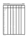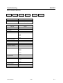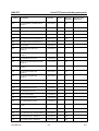
1
Service Manual
Vector Network Analyzers
R&S® ZVT8, R&S® ZVT20
1300.0000.08, 1300.0000.20
Printed in Germany
Test and Measurement
1300.0045.82-03
R&S® is a registered trademark of Rohde & Schwarz GmbH & Co. KG.
Trade names are trademarks of the owners.
The instrument includes software developed by the OpenSSL Project for use in the OpenSSL Toolkit
(http://www.openssl.org/). It includes cryptographic software written by Eric Young ([email protected]) and
software written by Tim Hudson ([email protected]). The verbatim license texts are provided in on the user
documentation CD-ROM (included in delivery).
R&S ZVT
Index
Index
Function..................................................................... 3.13
Replacement.............................................................. 3.24
A
L
Alignment ...................................................................... 2.3
Frequency accuracy .................................................... 2.6
Frequency response correction .............................2.7, 2.9
Level accuracy ............................................................ 2.9
Manual ........................................................................ 2.4
Reference frequency ................................................... 2.6
Test equipment............................................................ 2.4
Level accuracy
Alignment..................................................................... 2.9
Lithium battery
Replacement.............................................................. 3.20
M
B
Manual alignment .......................................................... 2.4
Mechanical Drawings..................................................... 5.4
Menu, service ................................................................ 2.3
Microwave converter
Replacement.............................................................. 3.45
Motherboard
Function..................................................................... 3.14
Replacement.............................................................. 3.31
Battery
Replacement ..............................................................3.20
Block circuit
diagram ....................................................................... 5.4
Board replacement
Detector A120 ...................................................3.43, 3.46
Fan.............................................................................3.30
Front hood..................................................................3.26
Front module processor A90 ......................................3.17
Frontend A100...................................................3.34, 3.38
Motherboard A10........................................................3.31
Power supply..............................................................3.29
Power supply..............................................................3.28
Switching foil ..............................................................3.24
Synthesizer A110 .......................................................3.44
Board Replacement
Battery........................................................................3.20
Boards
Overview ....................................................................3.16
Boot problems
Troubleshooting..........................................................3.51
O
OCXO
Function..................................................................... 3.10
Option
B4
Function .......................................................... 3.10
Installation ................................................................... 4.2
List............................................................................... 4.2
P
Password....................................................................... 2.3
Performance test
Frequency accuracy .................................................... 1.4
Harmonics suppression ............................................... 1.5
Level accuracy...................................................... 1.6, 1.7
Level linearity........................................................ 1.5, 1.8
Protocol ..................................................................... 1.15
Performance Test .......................................................... 1.1
Power cables ................................................................. 5.3
Power supply
Function..................................................................... 3.14
Replacement.............................................................. 3.29
Replacement.............................................................. 3.28
Power-up problems...................................................... 3.50
Precision attenuator
Function....................................................................... 3.8
D
Detector
Replacement .....................................................3.43, 3.46
documents .................................................................... 5.3
Documents .................................................................... 5.3
F
Fan
Replacement ..............................................................3.30
Frequency accuracy
Alignment .................................................................... 2.6
Check.......................................................................... 1.4
Frequency response
Correction..............................................................2.7, 2.9
Front hood....................................................................3.26
Front module processor
Function .....................................................................3.13
Replacement ..............................................................3.17
Front unit......................................................................3.13
Frontend
Repelcement .....................................................3.34, 3.38
Function description ...................................................... 3.1
R
Repairs .......................................................................... 3.1
Replacement
Boards ....................................................................... 3.15
Replacing
Boards ....................................................................... 3.15
S
I
Software update ............................................................ 4.1
Spare parts
electrical parts ............................................................. 5.4
list of all parts............................................................... 5.5
Synthesizer
Replacement.............................................................. 3.44
Instrument construction ................................................. 3.1
K
Keyboard
1300.0052.82
I-1
E-3
Index
R&S ZVT
Troubleshooting ......................................................... 3.48
Troubbleshooting
Power-up problems.................................................... 3.50
Troubleshooting
Boot problems............................................................ 3.51
Selftest ............................................................. 3.58, 3.63
Selftest ...................................................................... 3.53
T
Test equipment
Alignment .................................................................... 2.4
Performance test ......................................................... 1.2
Test equpment
1300.0052.82
I-2
E-3
Procedure in Case of Service and Ordering of Spare
Parts
This section contains information on shipping an instrument to your service center and ordering spare
parts.
Please contact your local Rohde & Schwarz service center if you need service or repair work of your
equipment or to order spare parts. The list of the Rohde & Schwarz representatives is provided at the
beginning of this service manual. You can find the current address of your representative on our
homepage www.rohde-schwarz.com. Navigate to Service & Support / Service Locations.
Shipping the Instrument
We require the following information in order to answer your inquiry fast and correctly and to determine
whether the warranty is still valid for your instrument:
●
●
●
●
●
●
●
Instrument model
Serial number
Firmware version
Must the instrument be returned with this firmware?
Detailed error description in case of repair
Indication of desired calibration
Contact person for possible questions
In some countries, an RMA process is available for the return shipment of the instrument. For details,
contact your local representative.
When shipping the instrument, be careful to provide for sufficient mechanical and antistatic protection.
●
●
Use the original packaging for transporting or shipping the instrument. The protective caps for the front
and rear prevent damage to the operating elements and the connectors.
If you do not use the original packaging, provide for sufficient padding to prevent the instrument from
slipping inside the box. Wrap antistatic packing foil around the instrument to protect it from electrostatic charging.
Rohde & Schwarz offers repair and calibrations of the test systems it produces. The calibration
documentation fulfills ISO 17025 requirements.
Shipping Defective Modules
Also when shipping a module, be careful to provide for sufficient mechanical and antistatic protection.
●
●
Ship the module in a sturdy, padded box.
Wrap the module in antistatic foil.
If the packaging is only antistatic but not conductive, additional conductive packaging is required. The
additional packaging is not required if the tightly fitting packaging is conductive.
Exception:
If the module contains a battery, the tightly fitting packaging must always consist of antistatic, nonchargeable material to protect the battery from being discharged.
1171.0200.61-01
1
Ordering Spare Parts
To deliver spare parts promptly and correctly, we need the following information:
●
●
●
●
●
●
●
●
Stock number (see list of spare parts in chapter "Documents")
Designation
Component number according to list of spare parts
Number of pieces
Instrument type for which the spare part is needed
Instrument stock number
Instrument serial number
Contact person for possible questions
Refurbished Modules
Refurbished modules are an economical alternative to original modules. Bear in mind that refurbished
modules are not new, but repaired and fully tested parts. They may have traces from use, but they are
electrically and mechanically equivalent to new modules.
Your Rohde & Schwarz representative will be happy to inform you about which modules are available as
refurbished modules.
Taking Back Defective Replaced Modules
Defective modules of the replacement program which cannot be repaired are taken back within three
months following delivery. A repurchasing value is credited.
Excluded are parts which cannot be repaired, e.g. printed boards that are burnt, broken or damaged by
attempts to repair them, incomplete modules, and parts with severe mechanical damage.
Please return the defective replacement modules, together with the accompanying document for returned
merchandise, which you received with the spare module. We need the following information:
●
●
●
●
●
●
●
Stock number, serial number and designation of the removed part
Detailed error description
Stock number, serial number and type of instrument from which the module was removed
Date of removal
Name of the engineer/technician who replaced the module
R&S ordering number
Service reference number (if available)
1171.0200.61-01
2
FSQ FVREF "Überschrift 2" \* MERGEFORMAT Fehler! Formatvorlage nicht definiert.
R&S ZVT
Contents Performance Test
Table of Contents - Chapter 1 "Performance Test"
1 Performance Test................................................................................................ 1.1
Preliminary Remarks ........................................................................................................................1.1
Test Equipment and Accessories ...................................................................................................1.2
Performance Test .............................................................................................................................1.4
Checking the Frequency Uncertainty .......................................................................................1.4
Checking the Harmonics ..........................................................................................................1.5
Checking the Maximum Output Power.....................................................................................1.6
Checking the Accuracy of Output Power..................................................................................1.7
Checking the Output Linearity ..................................................................................................1.8
Checking the Power Measurement Accuracy ..........................................................................1.9
Checking the Input Linearity...................................................................................................1.10
Checking the Input Noise Level..............................................................................................1.11
Checking the Matching (raw)..................................................................................................1.12
Checking the Dynamic Range................................................................................................1.13
Checking the DC Measurement Inputs ..................................................................................1.14
Performance Test Report...............................................................................................................1.15
1300.0052.82
I-1.1
E-3
R&S ZVT
Preliminary Remarks
1 Performance Test
Preliminary Remarks
•
The required characteristics of the network analyzer are checked after a warm-up time of at least
60 minutes; this ensures that the guaranteed data is met.
•
The values stated in the following sections are not guaranteed data; only the specifications in the data
sheet are binding.
•
The values in the data sheet are guaranteed limits. Because of the measurement errors that arise,
these limits must be increased to encompass the tolerances of the measuring equipment used for
the performance test.
•
Entries for the measurement are represented in the following way:
[<KEY>]
Press a front-panel key, e.g. [SPAN]
[<SOFTKEY>] Press a softkey, e.g. [MARKER -> PEAK]
[<nn unit>]
Enter a value + terminate the entry with a unit, e.g. [12 kHz]
Consecutive entries are separated with a [ : ], e.g. [ Meas Bandwidth : 1 kHz]
1300.0052.82
1.1
E-3
Performance Test
R&S ZVT
Test Equipment and Accessories
Item
Type of
equipment
Recommended characteristics or
features
Recommended R&S
model
Order No.
Application
1
Spectrum
analyzer
a) Counter mode:
Min. resolution: 100 Hz
Max. rel. frequency deviation: 10-6
b) Linearity
Max. departure from linearity (2 ):
0.06 dB
c) Frequency response:
50 MHz to 3.6 GHz: < 0.3 dB
3.6 GHz to 8 GHz: < 1.5 dB
8 GHz to 22 GHz: < 2 dB
22 GHz to 40 GHz: < 2.5 dB
R&S FSU 50
1166.1660.50
Frequency uncertainty
Harmonics
Output linearity
Input linearity
2
Power meter
300 kHz to 20 GHz
R&S NRVD
0857.8008.02 Max output power
Accuracy of output power
Power measurement
uncertainty
3
Power sensor
300 kHz to 8 GHz
R&S NRV-Z51
0857.9004.02
Max. output power
Accuracy of output power
Power measurement
uncertainty
oR&S ZVT8
3
Power sensor
10 MHz to 20 GHz
R&S NRV-Z52
0857.9204.02
Max. output power
Accuracy of output power
Power measurement
uncertainty
on R&S ZVT20
4
Calibration kit
N, 50
R&S ZV-Z21
1085.7099.02 Input linearity
Matching port 1 to port 8
Input noise level
on R&S ZVT8
4
Calibration kit
3.5mm, 50
R&S ZV-Z32
1128.3501.02 Input linearity
Matching port 1 to port 6
Input noise level
on R&S ZVA20
5
Signal
generator
300 kHz to 20 GHz,
Power = -40 dBm to 10 dBm
R&S SML01
R&S SMR27
with Option
R&S SMR-B15
1090.3000.11
1104.0002.27
. 300 kHz to 8 GHz.
. 10 MHz to 20 GHz.
Power measurement
uncertainty
1104.4989.02
6
Power splitter
N, 50 Ohm,
eq < 0.05 (50 MHz to 8 GHz)
Output tracking < 0.15 dB
Weinschel
1870A
-
Power measurement
uncertainty
on R&S ZVT8
5
Power splitter
3.5mm, 50 Ohm,
Output tracking < 0.25 dB
Weinschel
1593
-
Power measurement
uncertainty
on R&S ZVT20
7
Test cable
N(male) – N(male), approx. 1.5 m
1300.0052.82
Frequency uncertainty
Harmonics
Matching port 1 to port 8
Power measurement
uncertainty
Input linearity
on R&S ZVT8
1.2
E-3
R&S ZVT
Test Equipment and Accessories
Item
Type of
equipment
Recommended characteristics or
features
Recommended R&S
model
Order No.
Application
7
Test cable
Test cable 3.5 mm (m) to 3.5 mm (f).
R&S ZV-Z14
Frequency uncertainty
Harmonics
Matching port 1 to port 6
Power measurement
accuray
on R&S ZVA20
8
BNC cable
Male – male, approx. 1.5 m
9
DC power
supply
-12 V to +12 V
R&S NGSM
32/10
0192.0810.31
DC meas inputs
10
Multimeter
MU < 0.2%,
DC range 1 V, 10 V
R&S URE3
0350.5315.03
DC meas inputs
11
Conn. Cables
for DC inputs
R&S ZV-Z71
1164.1005.02
DC meas inputs
12
Monitor
13
Keyboard with
mouse
1300.0052.82
1134.4093.02
General:
Device synchronisation
General
USB connector
General
1.3
E-3
Performance Test
R&S ZVT
Performance Test
Compare with data sheet
Use a keyboard with mouse and an external monitor for all measurements (see Chapter “Test
Equipment“, Item 12 and 13). To show the hardkeys on the screen select Display \ Display Config \
Hardkey Bar.
Checking the Frequency Uncertainty
Instrument:
Spectrum analyzer (see Chapter “Test Equipment“, Item1)
Test cable (see Chapter “Test Equipment“, Item7)
Test setup:
Connect the spectrum analyzer to port 1 (port 2 to port 8)
Spectrum analyzer settings:
- [ PRESET ]
- [ FREQ : 1 GHz ]
- [ SPAN : 100 kHz ]
- [ BW : MANUAL RES BW : 2 kHz ]
- [ MARKER : MARKER MODE : FREQ COUNT ]
- [ AMPT : REF LEVEL : 10 dBm]
R&S® ZVT settings
- Select [System : Internal Reference]
- [ Preset ]
- [ Meas :Wave Quantities: a1 Src Port 1]
- [ Sweep : Sweep Type : CW Mode :
CW Frequency : 1 GHz; Power : 0 dBm]
- [ Sweep : Single : Restart]
Measurement:
Read off the frequency indicated by the marker.
Frequency deviation = marker value – 1 GHz
Max. frequency deviation .............................. see Performance Test Report
1300.0052.82
1.4
E-3
R&S ZVT
Performance Test
Checking the Harmonics
Instrument:
Spectrum analyzer (see Chapter "Test Equipment", Item1)
Test cable (see Chapter “Test Equipment", Item7)
Test setup:
Connect the spectrum analyzer to port1 (port 2 to port 8)
Spectrum analyzer settings:
Note:
Synchronize the reference oscillators in the spectrum analyzer and in the
R&S®ZVT.
- [ PRESET ]
- [ FREQ : fGEN, 2* fGEN, 3* fGEN *]
- [ SPAN : ZERO SPAN ]
- [ BW : MANUAL RES BW : 1 kHz ]
- [ MARKER : DETECTOR : RMS ]
- [ AMPT : REF LEVEL : 10 dBm]
* For measurement frequencies, see Performance Test Report {fGEN}.
R&S® ZVT settings:
- [ Preset ]
- [ Meas : Wave Quantities: a1 Src Port 1
(a2 Src Port 2 to a8 Src Port 8)]
- [ Sweep : Sweep Type : CW Mode :
CW Frequency : {fGEN*} ; Power : 8 dBm ]
- [ Sweep : Single : Restart]
* For measurement frequencies, see Performance Test Report {fGEN}.
Measurement:
Calculation:
Read off the levels Ln*fgen (n = 1, 2, 3) indicated by the spectrum
analyzer’s markers.
Harmonics = Ln*f gen - Lfgen - cable loss (in dB)
The cable loss corresponds to the S21 of the test cable used between the
fundamental and the measured harmonic (S21 is negative).
1300.0052.82
1.5
E-3
Performance Test
R&S ZVT
Checking the Maximum Output Power
Instrument:
Power sensor or
Power meter with power sensor
(see Chapter “Test Equipment“, Item2)
Test setup:
Connect power sensor to port1 (port 2 to port 8)
Power sensor settings:
For measurement frequencies, see Performance Test Report {fGEN*}.
R&S®ZVT settings:
- [ Preset ]
- [ Meas : Wave Quantities: a1 Src Port 1
(a2 Src Port 2 to a8 Src Port 8)]
- [ Sweep : Sweep Type : CW Mode :
CW Frequency : {fGEN*} ; Power : 16 dBm]
- [ Sweep : Single : Restart]
* For measurement frequencies see the Performance Test Report {fGEN}.
Measurement:
Read off the level indicated by the power meter.
Max. power ................................................... see Performance Test Report
1300.0052.82
1.6
E-3
R&S ZVT
Performance Test
Checking the Accuracy of Output Power
Instrument:
Power sensor or
Power meter with power sensor
(see Chapter “Test Equipment“, Item2)
Test setup:
Connect the power sensor to port 1 (port 2 to port 8)
Power sensor settings:
For measurement frequencies, see Performance Test Report {fGEN*}.
R&S®ZVT settings:
- [ Preset ]
- [ Mode : ALC : on ]
- [ Meas : Wave Quantities: a1 Src Port 1
(a2 Src Port 2, a3 Src Port 3, a8 Src Port 8)]
- [ Sweep : Sweep Type : CW Mode :
CW Frequency : {fGEN*} ; Power : -10 dBm]
- [ Sweep : Single : Restart]
* For measurement frequencies, see Performance Test Report {fGEN}.
Measurement:
Read off the levels indicated by the power sensor
Level deviation = LSENSOR – (-10 dBm)
1300.0052.82
1.7
E-3
Performance Test
R&S ZVT
Checking the Output Linearity
Instrument:
Spectrum analyzer (see Chapter “Test Equipment“, Item1)
Test cable (see Chapter “Test Equipment“, Item7)
Test setup:
Connect the spectrum analyzer to port 1(port 2 to port 8)
Spectrum analyzer settings:
Note:
Synchronize the reference oscillators in the spectrum analyzer and in the
R&S®ZVT :
- [ PRESET ]
- [ FREQ : fGEN*]
- [ SPAN : ZERO SPAN ]
- [ BW : MANUAL RES BW : 1 kHz ]
- [ MARKER : DETECTOR : RMS ]
- [ AMPT : REF LEVEL : 5 dBm]
* For measurement frequencies, see Performance Test Report {fGEN}.
R&S®ZVT settings:
- [ Preset ]
- [ Meas : Wave Quantities: a1 Src Port 1
(a2 Src Port 2 to a8 Src Port 8)]
- [ Sweep : Sweep Type : CW Mode :
CW Frequency : {fGEN*} ; Power : {lGEN*}]
- [ Sweep : Single : Restart]
* For measurement frequencies {fGEN} and levels {lGEN}, see
Performance Test Report
Measurement:
Calculation:
Read the spectrum analyzer’s marker values (level L) .
The measured values are referred to the level at the R&S ZVT setting
of-10 dBm.
Calculating the generator level linearity:
Level linearity = L - L@-10dBm – step width (in dB)
Step width = lgen – (-10 dBm) (reference)
1300.0052.82
1.8
E-3
R&S ZVT
Performance Test
Checking the Power Measurement Accuracy
Instrument:
Power sensor or
Power meter with power sensor
(see Chapter “Test Equipment“, Item2)
Signal generator (see Chapter “Test Equipment“, Item5)
Power splitter (see Chapter “Test Equipment“, Item6)
Calibration kit (see Chapter “Test Equipment“, Item4)
Test cable (see Chapter “Test Equipment“, Item7)
Preparation/
test setup:
Connect the signal generator to the power-splitter input using the test
cable.
Connect the power sensor to a power-splitter output
Connect the other power-splitter output to port1 (port2 to port 8) using an
adapter from the calibration kit
R&S®ZVT settings:
The reference oscillators in the signal generator and in the R&S ZVT must
be synchronized.
- [ Preset ]
- [ Meas : Wave Quantities: b1 Src Port 1
(b2 Src Port 2 to b4 Src Port 4)]
- [ Power : RF Off ]
- [ Meas Bandwidth : 100 Hz ]
- [ Marker ]
- [ Sweep : Sweep Type : CW Mode :
CW Frequency : {fGEN*}]
- [ Sweep : Single : Restart]
* For the measurement frequencies, see Performance Test Report
{fGEN}.
Measurement:
Signal generator : CW Mode, Frequency: fgen
Signal-generator level: -5 dBm
Adjust the signal-generator level so that the power meter
reads 0 dB +/- 0.2 dB
Determine the signal-generator level that gives –10 dBm at the splitter
output. This level is required for the following measurement, “Checking
Receiver Linearity”.
Read off the power meter display and the ZVT marker values.
Level error = LZVT – LPS
1300.0052.82
1.9
E-3
Performance Test
R&S ZVT
Checking the Input Linearity
Instrument:
Calibration kit (see Chapter “Test Equipment“, Item4)
R&S®ZVT settings:
- [ Preset ]
- [ Meas : Ratios: b1/a1 Src Port 1 (b2/a2 Src Port 2 to b8/a8 Src Port 8)]
- [ Meas Bandwidth : 10 Hz ]
- [ Marker]
- [ Sweep : Sweep Type : Power : Start -40dBm : Stop 10dBm :
CW Frequency : {fGEN*}]
- [ Sweep : Single : Restart]
* For measurement frequencies, see Performance Test Report {fGEN}
1. Test setup:
Connect an open male to port 1 (port 2 to port 4)
1. Measurement:
- [ Trace Funct ]
- [ Data -> Mem ]
- [ Show Mem : off ]
2. Test setup:
Connect a short male to port 1 (port 2 to port 4)
2. Measurement:
- [ Math = Data/Mem : on ]
Set
Ref Marker to -10dBm
Select Delta Mode
Set
Marker1 to -40dBm up to +10dBm by 5dB steps
Read off the differences of the Marker Values displayed by the R&S ZVT
1300.0052.82
1.10
E-3
R&S ZVT
Performance Test
Checking the Input Noise Level
Test equipment
Calibration kit
(see Chapter “Test Equipment“, Item4)
Test setup:
Connect the Match Male from the calibration kit to port 1 (port 2 to port 8)
R&S®ZVT settings:
- [ Preset ]
- [ Meas : Wave Quantities: b1 Src Port 1
(b2 Src Port 2 to b8 Src Port 8)]
- [ Power : RF Off ]
- [ Meas Bandwidth : 10 Hz ]
- [ Marker ]
- [ Sweep : Sweep Type : CW Mode : CW Frequency : {fGEN*}]
- Service Function 1.0.0.1.1 (see chapter 3 ‘Service Functions’, Service
Level 2)
- [ Measure : Wave Quantities : More Wave Quantities… : Properties :
Detector : RMS : Meas. Time: 500ms]
- [ Sweep : Single : Restart]
* For measurement frequencies, see Performance Test Report {fGEN}.
Measurement:
1300.0052.82
Read off the noise level indicated by the markers on the DUT.
1.11
E-3
Performance Test
R&S ZVT
Checking the Matching (raw)
Instrument:
Calibration kit (see Chapter “Test Equipment“, Item4)
Test cable (see Chapter “Test Equipment“, Item7)
R&S®ZVT settings:
- [ Preset ]
- [ Power : 0 dBm ]
1. Preparation/
test setup:
Connect the test cable to port 1 on the R&S®ZVT and perform a 1-port
calibration at the end of the cable.
Connect the end of the test cable to port 2 (port 3 to port 8) on the
R&S®ZVT.
R&S®ZVT settings:
- [ Meas : S11]
- [ Marker ]
- [ Add Channnel + Trace ]
- [ Meas : S22 (S33 to S88) ]
- [ Power : -40 dBm ]
- [ Trace Funct ]
- [ Show Data : off ]
- [ Trace Select : Trc 1 ]
1. Measurement
Read off the network analyzer’s marker values (for marker frequencies
see Performance Test Report)
R&S®ZVT settings:
- [ Power : -40 dBm ]
- [ Trace Funct ]
- [ Show Data : off ]
- [ Trace Select : Trc 2 ]
- [ Trace Funct ]
- [ Show Data : on ]
- [ Meas : S22]
- [ Marker ]
2. Preparation/
test setup:
Set port 2 power to 0 dBm
Connect the test cable to port 2 on the R&S®ZVT and perform a 1-port
calibration at the end of the cable.
Connect the end of the test cable to port 1 on the R&S®ZVT.
2. Measurement
1300.0052.82
Read off the network analyzer’s marker values (for marker frequencies
see Performance Test Report)
1.12
E-3
R&S ZVT
Performance Test
Checking the Dynamic Range
Note: In case of reflectometer repair (reflectometer, coupler, cables) or reflectometer removing and
reinstalling a dynamic range check with 201 points (ZVT8) or 301 points (ZVT20) must be
performed (see chapter 3) before this performance test procedure.
Test equipment:
Calibration kit N
(see Chapter “Test Equipment“, Item4)
Test setup:
Connect Short Male to port1 and port 2 (port 3 to port 8)
(use Short Female with Through Male as a second Short Male)
R&S®ZVT settings:
- [ Preset ]
- [ Meas : Ratios : b1/a2 Drive Port 1]
- [ Power : max. spec. power ]
- [ Meas Bandwidth : 10 Hz ]
- [ Marker ]
- [ Sweep : Sweep Type : CW Mode : CW Frequency : {fGEN*}]
- Service Function 1.0.0.1.1 (see chapter 3 "Service Functions", Service
Level 2)
- [ Measure : Wave Quantities : More Wave Quantities… : Properties :
Detector : RMS : Meas. Time : 500ms]
- [ Sweep : Single : Restart]
* For measurement frequencies, see Performance Test Report {fGEN}.
Measurement:
Read off marker value
R&S®ZVT settings:
- [ Meas : Ratios : b2/a1 Drive Port 1]
[ Meas : Ratios : b3/a1 Drive Port 1]
[ Meas : Ratios : b4/a1 Drive Port 1]
[ Meas : Ratios : b5/a1 Drive Port 1]
[ Meas : Ratios : b6/a1 Drive Port 1]
[ Meas : Ratios : b7/a1 Drive Port 1]
[ Meas : Ratios : b8/a1 Drive Port 1]
- [ Sweep : Single : Restart]
* For measurement frequencies, see Performance Test Report {fGEN}.
Measurement:
Read off marker value
Calculation:
Dynamic range = Marker value + Power value
1300.0052.82
1.13
E-3
Performance Test
R&S ZVT
Checking the DC Measurement Inputs
Test equipment:
DC Power Supply NGSM 32/10 (see Chapter “Test Equipment“, Item9)
Multimeter URE3 (see Chapter “Test Equipment“, Item10)
DC cable (see Chapter “Test Equipment“, Item11)
Test setup:
Connect the Power Supply to the Input DC MEAS 1V (DC MEAS 10V) of
the ZVT using the DC cable
R&S®ZVT settings:
- [ Preset ]
For DC Meas 1 V:
- [ Meas : More : DC Inputs : DC Meas ±1 V]
- [ Format : Real]
- [ Scale : Scale/Div : .25 x1]
- [ Marker ]
For DC Meas 10 V:
- [ Meas : More : DC Inputs : DC Meas ±10 V]
- [ Format : Real]
- [ Scale : Scale/Div : 2.5 x1]
- [ Marker ]
Measurement:
Set Power Supply to DC values UDC using Multimeter URE (DC values
see Performance Test Report) and connect it to pos. and neg. input
Read off the DC level UDC ZVT indicated by the marker.
Calculation:
1300.0052.82
Deviation = UDC - UDC ZVT
1.14
E-3
R&S ZVT
Performance Test Report
Performance Test Report
Table 1-1:
Performance Test Report
ROHDE & SCHWARZ
Model ZVT
Options:
Item number:
Serial number
Performance Test Report
R&S ZVT Version 08.05.08
1300.0000
Tested by:
Date:
Signature:
General: All Tables apply to port1; values for ports 2 to 8 are identical.
Parameter
Covered on
Min. value
Actual value
Max. value
Unit
Measurement
tolerance
Frequency deviation
@ 1 GHz
With Option
R&S ZVAB-B4
1300.0052.82
Hz
Page 1.4
- 8000
_________
1 Hz
+ 8000
+ 100
- 100
1.15
E-3
Performance Test Report
Covered on
R&S ZVT
Min. value
Actual value
Max. value
Unit
Measurement
tolerance
Port __
Harmonics
Source power:
ZVT8 +8dBm
ZVT20 +10 dBm
Freq.
Harmonics
50 MHz 100 MHz
150 MHz
Page 1.4
dBc
________
________
-20
-20
100 MHz 200 MHz
300 MHz
________
________
-20
-20
200 MHz 400 MHz
600 MHz
________
________
-20
-20
500 MHz 1000 MHz
1500 MHz
________
________
-20
-20
750 MHz 1500 MHz
2250 MHz
________
________
-20
-20
1 GHz
________
________
-20
-20
1.5 GHz 3 GHz
4.5 GHz
________
________
-20
-20
2 GHz
________
________
-20
-20
2.1 GHz 4.2 GHz
6.3 GHz
________
________
-20
-20
2.5 GHz 5.0 GHz
7.5 GHz
________
________
-20
-20
3.0 GHz 6.0 GHz
9.0 GHz
________
________
-20
-20
3.5 GHz 7 GHz
10.5 GHz
________
________
-20
-20
4.0 GHz 8.0 GHz
12.0 GHz
________
________
-20
-20
4.1 GHz 8.2 GHz
12.3 GHz
________
________
-20
-20
5.0 GHz 10.0 GHz
15.0 GHz
________
________
-20
-20
2 GHz
3 GHz
4 GHz
6 GHz
1300.0052.82
1.16
1 dB
E-3
R&S ZVT
Port __
Harmonics
Source power:
ZVT8 +8dBm
ZVT20 +10 dBm
Freq.
Harmonics
5.04 GHz 10.08 GHz
15.12 GHz
Performance Test Report
Page 1.4
dBc
________
________
-20
-20
5.05 GHz 10.10 GHz
15.15 GHz
________
________
-20
-20
6.0 GHz 12.0 GHz
18.0 GHz
________
________
-20
-20
6.35 GHz 12.70 GHz
19.05 GHz
________
________
-20
-20
6.36 GHz 12.72 GHz
19.08 GHz
________
________
-20
-20
7.0 GHz 14.0 GHz
21.0 GHz
________
________
-20
-20
8.0 GHz 16.0 GHz
24.0 GHz
________
________
-20
-20
ZVT20 only:
9.0 GHz 18.0 GHz
________
-20
11.0 GHz 22.0 GHz
________
-20
1300.0052.82
1.17
1 dB
E-3
Performance Test Report
Covered on
R&S ZVT
Min. value
Actual value
Max. value
Unit
Measurement
tolerance
Port __
Max. output power
Page 1.5
dBm
Test frequency
ZVT8 only:
300 kHz
1 MHz
2 MHz
5 MHz
10 MHz
20 MHz
50 MHz
100 MHz
200 MHz
500 MHz
750 MHz
1.0 GHz
1.5 GHz
2.0 GHz
2.1 GHz
2.5 GHz
3.0 GHz
3.5 GHz
4.0 GHz
4.1 GHz
4.5 GHz
5.0 GHz
5.05 GHz
5.7 GHz
6.0 GHz
6.35 GHz
6.36 GHz
7.0 GHz
7.5 GHz
8.0 GHz
10
10
10
10
10
10
13
13
13
13
13
13
13
13
13
13
13
13
13
10
10
10
10
10
10
10
10
10
8
8
________
________
________
________
________
________
________
________
________
________
________
________
________
________
________
________
________
________
________
________
________
________
________
________
________
________
________
________
________
________
ZVT20 only:
10 MHz
20 MHz
50 MHz
100 MHz
200 MHz
500 MHz
750 MHz
1.0 GHz
1.5 GHz
2.0 GHz
2.1 GHz
2.5 GHz
3.0 GHz
10
10
10
10
10
10
10
10
10
10
10
10
10
________
________
________
________
________
________
________
________
________
________
________
________
________
1300.0052.82
1.18
1 dB
E-3
R&S ZVT
Performance Test Report
Page 1.5
3.5 GHz
4.0 GHz
4.1 GHz
4.5 GHz
5.0 GHz
5.05 GHz
5.7 GHz
6.0 GHz
6.35 GHz
6.36 GHz
7.0 GHz
7.5 GHz
8.0 GHz
8.1 GHz
10.0 GHz
10.1GHz
12.6 GHz
13 GHz
16.0 GHz
16.1 GHz
18.0 GHz
20.0GHz
1300.0052.82
dBm
10
10
10
10
10
10
10
10
10
10
10
10
10
10
10
10
10
10
5
3
3
3
1 dB
________
________
________
________
________
________
________
________
________
________
________
________
________
________
________
________
________
________
________
________
________
________
1.19
E-3
Performance Test Report
Parameter
Covered on
R&S ZVT
Min. value
Actual value
Max. value
Unit
Measurement
tolerance
Port . __
Power Uncertainty
output power
-10 dBm
Page 1.6
dB
Test frequency
ZVT8 only:
300 kHz
1 MHz
2 MHz
5 MHz
10 MHz
20 MHz
50 MHz
100 MHz
200 MHz
–2
–2
–2
–2
–2
–2
– 0.8
– 0.8
– 0.8
________
________
________
________
________
________
________
________
________
2
2
2
2
2
2
0.8
0.8
0.8
ZVT20 only:
10 MHz
20 MHz
50 MHz
100 MHz
200 MHz
–3
–3
–3
–3
–3
________
________
________
________
________
3
3
3
3
3
ZVT8 and ZVT20:
500 MHz
750 MHz
1.0 GHz
1.5 GHz
2.0 GHz
2.1 GHz
2.5 GHz
3.0 GHz
3.5 GHz
4.0 GHz
4.1 GHz
4.5 GHz
5.0 GHz
5.05 GHz
5.7 GHz
6.0 GHz
6.35 GHz
6.36 GHz
7.0 GHz
7.5 GHz
8.0 GHz
– 0.8
– 0.8
– 0.8
– 0.8
– 0.8
– 0.8
– 0.8
– 0.8
– 0.8
– 0.8
– 0.8
– 0.8
– 0.8
– 0.8
– 0.8
– 0.8
– 0.8
– 0.8
– 0.8
– 0.8
– 0.8
________
________
________
________
________
________
________
________
________
________
________
________
________
________
________
________
________
________
________
________
________
0.8
0.8
0.8
0.8
0.8
0.8
0.8
0.8
0.8
0.8
0.8
0.8
0.8
0.8
0.8
0.8
0.8
0.8
0.8
0.8
0.8
1300.0052.82
1.20
0. dB
E-3
R&S ZVT
Parameter
Performance Test Report
Covered on
Min. value
Actual value
Max. value
Unit
Measurement
tolerance
ZVT20 only:
8.1 GHz
10.0 GHz
10.1 GHz
12.6 GHz
12.7 GHz
16.0 GHz
16.1 GHz
18.0 GHz
20.0 GHz
1300.0052.82
– 0.8
– 0.8
– 0.8
– 0.8
– 0.8
– 0.8
– 0.8
– 0.8
– 0.8
________
________
________
________
________
________
________
________
________
1.21
0.8
0.8
0.8
0.8
0.8
0.8
0.8
0.8
0.8
E-3
Performance Test Report
Parameter
Covered on
R&S ZVT
Min. value
Actual value
Max. value
Unit
Measurement
tolerance
Port . __
Power linearity
Reference –10 dBm
Freq.
Level
50 MHz 20 dB
15 dB
10 dB
5 dB
-5 dB
-10 dB
-15 dB
-20 dB
ZVT8
-25 dB
only
-30 dB
Page 1.7
dB
-2
-2
-2
-2
-2
-2
-2
-2
-2
-2
________
________
________
________
________
________
________
________
________
________
2
2
2
2
2
2
2
2
2
2
500 MHz 20 dB
15 dB
10 dB
5 dB
-5 dB
-10 dB
-15 dB
-20 dB
ZVT8
-25 dB
only
-30 dB
- 0.8
- 0.8
- 0.8
- 0.8
- 0.8
- 0.8
- 0.8
- 0.8
- 0.8
- 0.8
________
________
________
________
________
________
________
________
________
________
0.8
0.8
0.8
0.8
0.8
0.8
0.8
0.8
0.8
0.8
1 GHz
20 dB
15 dB
10 dB
5 dB
-5 dB
-10 dB
-15 dB
-20 dB
-25 dB
-30 dB
- 0.8
- 0.8
- 0.8
- 0.8
- 0.8
- 0.8
- 0.8
- 0.8
- 0.8
- 0.8
________
________
________
________
________
________
________
________
________
________
0.8
0.8
0.8
0.8
0.8
0.8
0.8
0.8
0.8
0.8
20 dB
15 dB
10 dB
5 dB
-5 dB
-10 dB
-15 dB
-20 dB
-25 dB
-30 dB
- 0.8
- 0.8
- 0.8
- 0.8
- 0.8
- 0.8
- 0.8
- 0.8
- 0.8
- 0.8
________
________
________
________
________
________
________
________
________
________
0.8
0.8
0.8
0.8
0.8
0.8
0.8
0.8
0.8
0.8
ZVT8
only
2 GHz
ZVT8
only
1300.0052.82
1.22
0.06 dB
E-3
R&S ZVT
Parameter
Performance Test Report
Covered on
Min. value
Actual value
Max. value
Unit
Measurement
tolerance
Port . __
Power linearity
Reference –10 dBm
Freq.
Level
2.1 GHz 20 dB
15 dB
10 dB
5 dB
-5 dB
-10 dB
-15 dB
-20 dB
ZVT8
-25 dB
only
-30 dB
Page 1.7
dB
- 0.8
- 0.8
- 0.8
- 0.8
- 0.8
- 0.8
- 0.8
- 0.8
- 0.8
- 0.8
________
________
________
________
________
________
________
________
________
________
0.8
0.8
0.8
0.8
0.8
0.8
0.8
0.8
0.8
0.8
20 dB
15 dB
10 dB
5 dB
-5 dB
-10 dB
-15 dB
-20 dB
-25 dB
-30 dB
- 0.8
- 0.8
- 0.8
- 0.8
- 0.8
- 0.8
- 0.8
- 0.8
- 0.8
- 0.8
________
________
________
________
________
________
________
________
________
________
0.8
0.8
0.8
0.8
0.8
0.8
0.8
0.8
0.8
0.8
20 dB
15 dB
10 dB
5 dB
-5 dB
-10 dB
-15 dB
-20 dB
-25 dB
-30 dB
- 0.8
- 0.8
- 0.8
- 0.8
- 0.8
- 0.8
- 0.8
- 0.8
- 0.8
- 0.8
________
________
________
________
________
________
________
________
________
________
0.8
0.8
0.8
0.8
0.8
0.8
0.8
0.8
0.8
0.8
4.1 GHz 20 dB
15 dB
10 dB
5 dB
-5 dB
-10 dB
-15 dB
-20 dB
ZVT8
-25 dB
only
-30 dB
- 0.8
- 0.8
- 0.8
- 0.8
- 0.8
- 0.8
- 0.8
- 0.8
- 0.8
- 0.8
________
________
________
________
________
________
________
________
________
________
0.8
0.8
0.8
0.8
0.8
0.8
0.8
0.8
0.8
0.8
3 GHz
ZVT8
only
4 GHz
ZVT8
only
1300.0052.82
1.23
0.06 dB
E-3
Performance Test Report
Parameter
Covered on
R&S ZVT
Min. value
Actual value
Max. value
Unit
Measurement
tolerance
Port . __
Power linearity
Reference –10 dBm
Freq.
7 GHz
Page 1.7
dB
Level
20 dB
15 dB
10 dB
5 dB
-5 dB
-10 dB
-15 dB
-20 dB
-25 dB
-30 dB
- 0.8
- 0.8
- 0.8
- 0.8
- 0.8
- 0.8
- 0.8
- 0.8
- 0.8
- 0.8
________
________
________
________
________
________
________
________
________
________
0.8
0.8
0.8
0.8
0.8
0.8
0.8
0.8
0.8
0.8
ZVT8 only:
8 GHz
18 dB
15 dB
10 dB
5 dB
-5 dB
-10 dB
-15 dB
-20 dB
ZVT8
-25 dB
only
-30 dB
- 0.8
- 0.8
- 0.8
- 0.8
- 0.8
- 0.8
- 0.8
- 0.8
- 0.8
- 0.8
________
________
________
________
________
________
________
________
________
________
0.8
0.8
0.8
0.8
0.8
0.8
0.8
0.8
0.8
0.8
ZVT20 only:
9 GHz
20 dB
15 dB
10 dB
5 dB
-5 dB
-10 dB
-15 dB
-20 dB
- 0.8
- 0.8
- 0.8
- 0.8
- 0.8
- 0.8
- 0.8
- 0.8
________
________
________
________
________
________
________
________
0.8
0.8
0.8
0.8
0.8
0.8
0.8
0.8
- 0.8
- 0.8
- 0.8
- 0.8
- 0.8
- 0.8
- 0.8
- 0.8
________
________
________
________
________
________
________
________
0.8
0.8
0.8
0.8
0.8
0.8
0.8
0.8
ZVT8
only
11 GHz
20 dB
15 dB
10 dB
5 dB
-5 dB
-10 dB
-15 dB
-20 dB
1300.0052.82
1.24
0.06 dB
E-3
R&S ZVT
Parameter
Performance Test Report
Covered on
Min. value
Actual value
Max. value
Unit
Measurement
tolerance
ZVT20 only:
Port . __
Power linearity
Reference –10 dBm
Page 1.7
dB
Freq.
13 GHz
Level
20 dB
15 dB
10 dB
5 dB
-5 dB
-10 dB
-15 dB
-20 dB
- 0.8
- 0.8
- 0.8
- 0.8
- 0.8
- 0.8
- 0.8
- 0.8
________
________
________
________
________
________
________
________
0.8
0.8
0.8
0.8
0.8
0.8
0.8
0.8
16 GHz
15 dB
10 dB
5 dB
-5 dB
-10 dB
-15 dB
-20 dB
- 0.8
- 0.8
- 0.8
- 0.8
- 0.8
- 0.8
- 0.8
________
________
________
________
________
________
________
0.8
0.8
0.8
0.8
0.8
0.8
0.8
17 GHz
13 dB
10 dB
5 dB
-5 dB
-10 dB
-15 dB
-20 dB
- 0.8
- 0.8
- 0.8
- 0.8
- 0.8
- 0.8
- 0.8
________
________
________
________
________
________
________
0.8
0.8
0.8
0.8
0.8
0.8
0.8
19 GHz
13 dB
10 dB
5 dB
-5 dB
-10 dB
-15 dB
-20 dB
- 0.8
- 0.8
- 0.8
- 0.8
- 0.8
- 0.8
- 0.8
________
________
________
________
________
________
________
0.8
0.8
0.8
0.8
0.8
0.8
0.8
20 GHz
13 dB
10 dB
5 dB
-5 dB
-10 dB
-15 dB
-20 dB
- 0.8
- 0.8
- 0.8
- 0.8
- 0.8
- 0.8
- 0.8
________
________
________
________
________
________
________
0.8
0.8
0.8
0.8
0.8
0.8
0.8
1300.0052.82
1.25
0.06 dB
E-3
Performance Test Report
Parameter
Covered on
R&S ZVT
Min. value
Actual value
Max. value
Unit
Measurement
tolerance
Page 1.8
dB
0.2 dB
Port . __
Power measurement
uncertainty
10 MHz
20 MHz
50 MHz
100 MHz
200 MHz
500 MHz
750 MHz
1 GHz
1.5 GHz
2 GHz
2.1 GHz
2.5 GHz
3 GHz
3.5 GHz
4 GHz
4.1 GHz
4.5 GHz
5.0 GHz
5.05 GHz
5.7 GHz
6.0 GHz
6.35 GHz
6.36 GHz
7.0 GHz
7.5 GHz
8.0 GHz
-1
-1
-1
-1
-1
-1
-1
-1
-1
-1
-1
-1
-1
-1
-1
-1
-1
-1
-1
-1
-1
-1
-1
-1
-1
-1
________
________
________
________
________
________
________
________
________
________
________
________
________
________
________
________
________
________
________
________
________
________
________
________
________
________
1
1
1
1
1
1
1
1
1
1
1
1
1
1
1
1
1
1
1
1
1
1
1
1
1
1
ZVT20 only:
9.0 GHz
11.0 GHz
13.0 GHz
15.0 GHz
17.0 GHz
19.0 GHz
20.0 GHz
-2
-2
-2
-2
-2
-2
-2
________
________
________
________
________
________
________
2
2
2
2
2
2
2
1300.0052.82
1.26
E-3
R&S ZVT
Parameter
Performance Test Report
Covered on
Min. value
Actual value
Max. value
Unit
Measurement
tolerance
Port . __
Input linearity ZVT8
Page 1.9
dB
0.06 dB
Reference –10 dBm
50 MHz
20 dB
15 dB
10 dB
5 dB
-5 dB
-10 dB
-15 dB
-20 dB
-25 dB
-30 dB
- 0.1
- 0.1
- 0.1
- 0.1
- 0.1
- 0.1
- 0.1
- 0.1
- 0.1
- 0.1
________
________
________
________
________
________
________
________
________
________
0.1
0.1
0.1
0.1
0.1
0.1
0.1
0.1
0.1
0.1
4 GHz
20 dB
15 dB
10 dB
5 dB
-5 dB
-10 dB
-15 dB
-20 dB
-25 dB
-30 dB
- 0.1
- 0.1
- 0.1
- 0.1
- 0.1
- 0.1
- 0.1
- 0.1
- 0.1
- 0.1
________
________
________
________
________
________
________
________
________
________
0.1
0.1
0.1
0.1
0.1
0.1
0.1
0.1
0.1
0.1
4.1 GHz 20 dB
15 dB
10 dB
5 dB
-5 dB
-10 dB
-15 dB
-20 dB
-25 dB
-30 dB
- 0.1
- 0.1
- 0.1
- 0.1
- 0.1
- 0.1
- 0.1
- 0.1
- 0.1
- 0.1
________
________
________
________
________
________
________
________
________
________
0.1
0.1
0.1
0.1
0.1
0.1
0.1
0.1
0.1
0.1
6 GHz
- 0.1
- 0.1
- 0.1
- 0.1
- 0.1
- 0.1
- 0.1
- 0.1
- 0.1
- 0.1
________
________
________
________
________
________
________
________
________
________
0.1
0.1
0.1
0.1
0.1
0.1
0.1
0.1
0.1
0.1
20 dB
15 dB
10 dB
5 dB
-5 dB
-10 dB
-15 dB
-20 dB
-25 dB
-30 dB
1300.0052.82
1.27
E-3
Performance Test Report
Parameter
Covered on
R&S ZVT
Min. value
Actual value
Max. value
Unit
Measurement
tolerance
Port . __
Input linearity ZVT8
Page 1.9
dB
0.06 dB
Reference –10 dBm
8 GHz
20 dB
15 dB
10 dB
5 dB
-5 dB
-10 dB
-15 dB
-20 dB
-25 dB
-30 dB
1300.0052.82
- 0.2
- 0.2
- 0.2
- 0.2
- 0.2
- 0.2
- 0.2
- 0.2
- 0.2
- 0.2
________
________
________
________
________
________
________
________
________
________
1.28
0.2
0.2
0.2
0.2
0.2
0.2
0.2
0.2
0.2
0.2
E-3
R&S ZVT
Performance Test Report
Parameter
Covered on
Port . __
Input linearity ZVT20
Page 1.9
Min. value
Actual value
Max. value
Unit
Measurement
tolerance
dB
0.06 dB
Reference –10 dBm
50 MHz 20 dB
15 dB
10 dB
5 dB
-5 dB
-10 dB
-15 dB
-20 dB
-25 dB
-30 dB
700 MHz
dB
20
15 dB
10 dB
5 dB
-5 dB
-10 dB
-15 dB
-20 dB
-25 dB
-30 dB
8 GHz
20 dB
15 dB
10 dB
5 dB
-5 dB
-10 dB
-15 dB
-20 dB
-25 dB
-30 dB
20 GHz 15 dB
10 dB
5 dB
-5 dB
-10 dB
-15 dB
-20 dB
-25 dB
-30 dB
1300.0052.82
- 0.1
- 0.1
- 0.1
- 0.1
- 0.1
- 0.1
- 0.1
- 0.1
- 0.1
- 0.1
________
________
________
________
________
________
________
________
________
________
0.1
0.1
0.1
0.1
0.1
0.1
0.1
0.1
0.1
0.1
- 0.1
- 0.1
- 0.1
- 0.1
- 0.1
- 0.1
- 0.1
- 0.1
- 0.1
- 0.1
________
________
________
________
________
________
________
________
________
________
0.1
0.1
0.1
0.1
0.1
0.1
0.1
0.1
0.1
0.1
- 0.3
- 0.3
- 0.3
- 0.1
- 0.1
- 0.1
- 0.1
- 0.1
- 0.1
- 0.1
________
________
________
________
________
________
________
________
________
________
0.3
0.3
0.3
0.1
0.1
0.1
0.1
0.1
0.1
0.1
- 0.3
- 0.3
- 0.1
- 0.1
- 0.1
- 0.1
- 0.1
- 0.1
- 0.1
________
________
________
________
________
________
________
________
________
0.3
0.3
0.1
0.1
0.1
0.1
0.1
0.1
0.1
1.29
E-3
Performance Test Report
Parameter
Covered on
Port . __
Input noise level
Page 1.10
R&S ZVT
Min. value
Actual value
Max. value
Measurement
tolerance
dBm
Test frequency
ZVT8 only:
423.450 kHz
1.12345 MHz
2.12345 MHz
5.12345 MHz
________
________
________
________
–70
–70
–70
–70
ZVT8 (ZVT20):
10.12345 MHz
20.12345 MHz
50.12345 MHz
100.12345 MHz
200.12345 MHz
500.12345 MHz
750.12345 MHz
1000.12345 MHz
1500.12345 MHz
2000.12345 MHz
2100.12345 MHz
2500.12345 MHz
3000.12345 MHz
3500.12345 MHz
3999.87655 MHz
4100.12345 MHz
4500.12345 MHz
5000.12345 MHz
5050.12345 MHz
5700.12345 MHz
6000.12345 MHz
6350.12345 MHz
6360.12345 MHz
7000.12345 MHz
7500.12345 MHz
7999.87655 MHz
________
________
________
________
________
________
________
________
________
________
________
________
________
________
________
________
________
________
________
________
________
________
________
________
________
________
–70
–70
–70
–110
–110
–110
–110
–110
–110
–110
–110
–110
–110
–110
–110
–105
–105
–105
–105
–105
–105
–105
–105
–105
–105
–105
ZVT20 only:
9000.12345 MHz
11000.12345 MHz
13000.12345 MHz
15000.12345 MHz
17000.12345 MHz
19000.12345 MHz
19999.87655 MHz
________
________
________
________
________
________
________
–100
–100
–100
–100
–100
–100
–100
1300.0052.82
Unit
1.30
_
_
_
_
(---)
(---)
(---)
(-70)
(-70)
(-70)
(-105)
(-105)
(-105)
(-105)
(-105)
(-105)
(-105)
(-105)
(-105)
_
_
_
_
_
_
_
_
_
_
_
_
_
_
_
_
_
_
_
_
_
_
_
_
_
_
_
_
_
_
_
_
_
E-3
R&S ZVT
Parameter
Performance Test Report
Covered on
Min. value
Actual value
Page 1.11
Max. value
Unit
Measurement
tolerance
dB
1 dB
Port . __
Matching (raw)
Test frequency
ZVT8 only:
300 kHz
1 MHz
2 MHz
5 MHz
16
16
16
16
ZVT8, (ZVT20):
10 MHz
20 MHz
50 MHz
100 MHz
200 MHz
500 MHz
750 MHz
1 GHz
1.5 GHz
2 GHz
2.5 GHz
3 GHz
3.5 GHz
4 GHz
4.5 GHz
5 GHz
5.5 GHz
6 GHz
6.5 GHz
7 GHz
7.5 GHz
8 GHz
16
16
16
16
16
16
16
16
16
16
16
16
16
16
16
16
16
16
16
16
14
14
ZVT20:
9.0 GHz
11.0 GHz
13.0 GHz
15.0 GHz
17.0 GHz
19.0 GHz
20.0 GHz
8
8
8
8
8
8
8
1300.0052.82
________
________
________
________
(10)
(10)
(16)
(16)
(16)
(16)
(16)
(16)
(16)
(16)
(8)
(8)
(8)
(8)
(8)
(8)
(8)
(8)
(8)
(8)
(8)
(8)
________
________
________
________
________
________
________
________
________
________
________
________
________
________
________
________
________
________
________
________
________
________
________
________
________
________
________
________
________
1.31
E-3
Performance Test Report
Parameter
Covered on
Port . __
Dynamic range ZVT8
Page 1.12
R&S ZVT
Min. value
Actual value
Max. value
Unit
Measurement
tolerance
dB
Test frequency
300 kHz
1 MHz
2 MHz
5 MHz
10 MHz
20 MHz
50 MHz
100 MHz
200 MHz
500 MHz
750 MHz
1 GHz
1.5 GHz
2 GHz
2.1 GHz
2.5 GHz
3 GHz
3.5 GHz
4 GHz
4.1 GHz
4.5 GHz
5 GHz
5.05 GHz
5.7 GHz
6 GHz
6.35 GHz
6.36 GHz
7 GHz
7.5 GHz
8 GHz
1300.0052.82
80
80
80
100
100
100
100
120
120
120
120
120
120
120
120
120
120
120
120
117
117
117
117
117
117
117
117
117
115
108
________
________
________
________
________
________
________
________
________
________
________
________
________
________
________
________
________
________
________
________
________
________
________
________
________
________
________
________
________
________
1.32
_
_
_
_
_
_
_
_
_
_
_
_
_
_
_
_
_
_
_
_
_
_
_
_
_
_
_
_
_
_
E-3
R&S ZVT
Performance Test Report
Parameter
Covered on
Port . __
Dynamic range ZVT20
Page 1.12
Min. value
Actual value
Max. value
Unit
Measurement
tolerance
dB
Test frequency
10 MHz
20 MHz
50 MHz
100 MHz
200 MHz
500 MHz
700 MHz
1 GHz
1.5 GHz
2 GHz
2.1 GHz
2.5 GHz
3 GHz
3.5 GHz
4 GHz
4.1 GHz
4.5 GHz
5 GHz
5.05 GHz
5.7 GHz
6 GHz
6.35 GHz
6.36 GHz
7 GHz
7.5 GHz
8 GHz
9.0 GHz
11.0 GHz
13.0 GHz
15.0 GHz
16.0 GHz
19.0 GHz
20.0 GHz
1300.0052.82
80
80
80
100
100
100
120
120
120
120
120
120
120
120
120
120
120
120
120
120
120
120
120
120
120
120
110
110
110
110
110
105
105
________
________
________
________
________
________
________
________
________
________
________
________
________
________
________
________
________
________
________
________
________
________
________
________
________
________
________
________
________
________
________
________
________
1.33
_
_
_
_
_
_
_
_
_
_
_
_
_
_
_
_
_
_
_
_
_
_
_
_
_
_
_
_
_
_
_
_
_
E-3
Performance Test Report
Parameter
Covered on
Accuracy
DC meas 1 V
Page 1.14
R&S ZVT
Min. value
Actual value
Max. value
Pos. Input
-1000 m V
-300 mV
-10 mV
10 mV
300 mV
1000 m V
- 27.5
- 10.0
- 2.75
- 2.75
- 10.0
- 27.5
________
________
________
________
________
________
+ 27.5
+ 10.0
+ 2.75
+ 2.75
+ 10.0
+ 27.5
Neg. Input
-1000 m V
-300 mV
-10 mV
10 mV
300 mV
1000 m V
- 27.5
- 10.0
- 2.75
- 2.75
- 10.0
- 27.5
________
________
________
________
________
________
+ 27.5
+ 10.0
+ 2.75
+ 2.75
+ 10.0
+ 27.5
Accuracy
DC meas 10 V
Page 1.14
Pos. Input
-10.0 V
-3.0 V
-0.1 V
0.1 V
3.0 V
10.0 V
- 0.275
- 0.10
- 0.0275
- 0.0275
- 0.10
- 0.275
________
________
________
________
________
________
+ 0.275
+ 0.10
+ 0.0275
+ 0.0275
+ 0.10
+ 0.275
Neg. Input
-10.0 V
-3.0 V
-0.1 V
0.1 V
3.0 V
10.0 V
- 0.275
- 0.10
- 0.0275
- 0.0275
- 0.10
- 0.275
________
________
________
________
________
________
+ 0.275
+ 0.10
+ 0.0275
+ 0.0275
+ 0.10
+ 0.275
1300.0052.82
1.34
Unit
Measurement
tolerance
mV
1 mV
V
0.01 V
E-3
R&S ZVT
Table of Contents - Alignment
Table of Contents - Chapter 2 "Alignment"
2 Alignment............................................................................................................. 2.3
Service Menu ...........................................................................................................................2.3
Manual Alignment and Recording Correction Values ..................................................................2.4
Test Equipment ........................................................................................................................2.4
Aligning the Frequency Accuracy.............................................................................................2.6
Aligning the DC Inputs..............................................................................................................2.7
Correction Value Recording and Factory System Error Calibration .........................................2.9
Installation of the Alignment Program ......................................................................................2.9
Checking the Gauge.................................................................................................................2.9
1300.0052.82
I-2.1
E-3
Table of Contents - Alignment
1300.0052.82
R&S ZVT
I-2.2
E-3
R&S ZVT
Manual Alignment and Recording Correction Values
2 Alignment
This chapter describes the alignment of the frequency reference and the recording of correction data
after a board has been replaced.
The following manual alignments or corrections can be performed on the R&S ZVT:
•
•
Alignment of the 10-MHz reference oscillator which determines the frequency accuracy of the
R&S ZVT
Recording the correction values for the generators and the receivers which determine the
measurement accuracy of the R&S ZVT’s absolute values.
By performing the alignment and recording the correction values, it is possible to ensure that the
R&S ZVT is meeting its specifications by correcting any deviations.
The alignments must be performed within an ambient temperature range of +22 °C to +24 °C after the
appropriate warm-up time.
The R&S ZVT meets its specs and is ready for operation when the alignment has been performed
and/or correction values have been recorded and a system error calibration carried out.
Service Menu
Access to the board-alignment functions is password-protected to prevent unintentional changes to
settings.
Entering the password
MENU
Service Function
System
System Config…
Measurement Wizard ?
Print
?
Enter Password:
@ Internal Reference
External Reference
Preset
GPIB Address…
Service Function…
External Tools
•
?
Enter password 30473035.
Caution
The alignment shall be performed only by appropriately trained personnel because any
changes made have a profound effect on the measurement accuracy of the instrument
1300.0052.82
2.3
E-3
Manual Alignment and Recording Correction Values
R&S ZVT
Manual Alignment and Recording Correction Values
In the sequel, the test equipment and the instrument preparations required to manually align the
R&S ZVT and each of the alignments are described.
Preliminary remarks
The analyzer must be allowed to warm up for at least 30 minutes before alignment. This is the only way
of ensuring that the guaranteed data are met.
Test Equipment
Table 2-1
Test equipment for manually aligning the R&S ZVT
Item
Type of equipment
Recommended
specifications
Recommended
model
R&S Order
No.
Application
1
Spectrum analyzer
Counter mode:
Min. resolution: 0.1 Hz
Max. rel. frequency
deviation: 10-9
R&S FSU 26
w. option
R&S FSU-B4
1129.9003.26
Frequency accuracy of
the reference oscillator
2
Signal generator
300 kHz to 20 GHz,
Power = -40 dBm to 10 dBm
R&S SML01
R&S SMR27
with Option
R&S SMR-B15
1090.3000.11
1104.0002.27
Recording correction
values
1104.4989.02
3
Power meter
300 kHz to 20 GHz
R&S NRVD
0857.8008.02
Recording correction
values
4
Power sensor
300 kHz to 8 GHz
R&S NRV-Z51
0857.9004.02
Recording correction
values on R&S ZVT8
4
Power sensor
10 MHz to 20 GHz
R&S NRV-Z52
0857.9204.02
Recording correction
values on R&S ZVT20
5
Power splitter
N, 50 Ohm,
eq < 0.05 (50 MHz to 8 GHz)
Output tracking < 0.15 dB
Weinschel
1870A
-
Recording correction
values on R&S ZVT8
5
Power splitter
3.5mm, 50 Ohm,
Output tracking < 0.25 dB
Weinschel 1593 -
6
PC with
Pentium, WinXP, WinNT
GPIB-Interface
1072.6101.00
1302.4460.00
Alignment Software
R&S ZVAB-Service
8
Power supply
2x 0 to 10 V
9
DC meter
1300.0052.82
Recording correction
values
GR AT-GPIB IEEE4888 IF PCI NI-488 PCI-GPIB
National Instruments
7
Recording correction
values on R&S ZVT20
Recording correction
values
Aligning the DC inputs
R&S URE 3
2.4
0350.5315.03
Aligning the DC inputs
E-3
R&S ZVT
Manual Alignment and Recording Correction Values
Item
Type of equipment
Recommended
specifications
Recommended
model
R&S Order
No.
Application
10
Calibration kit
N calibration kit
R&S ZV-Z21
1085.7099.02
Recording correction
values on ZVT8
10
Calibration kit
3.5 mm, 50
to 20 GHz.
R&S ZV-Z32
1128.3501.02
Recording correction
values on R&S ZVT20
11
Test cable
Test cable N (m) to N (m).
R&S ZV-Z11
1085.6505.03
Recording correction
values on R&S ZVT8
11
Test cable
Test cable 3,5mm (m)
to 3.5 mm (f).
R&S ZV-Z14
1134.4093.02
Recording correction
values on R&S ZVT20
12
Conn. Cables for DC
Inputs
4-pin mini-DIN plug
R&S ZV-Z71
1164.1005.02
Aligning the DC inputs
1300.0052.82
. 10 MHz
2.5
E-3
Manual Alignment and Recording Correction Values
R&S ZVT
Aligning the Frequency Accuracy
Test equipment
Spectrum analyzer (section "Test Equipment", item 1):
-9
Error <1x10
Test setup:
Connect the frequency counter to the 10-MHz reference output at the
rear of the R&S ZVT.
R&S ZVT settings:
Select internal reference
MENU : System: Reference Internal
Spectrum analyzer settings:
Center frequency: 10 MHz
Span: 200 Hz
Note:
Before the following measurement is performed, the R&S ZVT must
have been switched on for at least 30 minutes to give the reference
oscillator time to warm up.
Measurement:
Measure the frequency with the frequency counter:
Nominal frequency:
Model without OCXO (Option B4) 10 MHz ± 80 Hz
Model with OCXO (Option B4) 10 MHz ± 1 Hz
Alignment without Option R&S ZVAB-B4:
•
Enter Service Function 2.1.1.6.209.0x000000
•
Read off the frequency-counter display, e.g. 10.000050 MHz.
•
Change the right-hand segment (corresponding to bit 0 to bit 11) of the data word - e.g. to
000400 - instead of 000000.
•
Read off the frequency counter display again, e.g. 10.000010 MHz.
•
Change the right-hand segment of the data word (000000 to 0007FF), until the counter indicates
precisely 10.000000 MHz.
Alignment with Option R&S ZVAB-B4:
•
Enter Service Function 2.1.1.6.209.0x800000.
•
Read off the frequency-counter display, e.g. 10.000005 MHz.
•
Change the left-hand segment (corresponding to bit 12 to bit 23) of the data word - e.g. to
400000 - instead of 800000.
•
Read off the frequency-counter display again, e.g. 10.000001 MHz.
•
Change the left-hand segment of the data word (000000 to 800000), until the counter indicates
precisely 10.000000 MHz.
1300.0052.82
2.6
E-3
R&S ZVT
Manual Alignment and Recording Correction Values
Writing data to the hard disk:
Change to computer application
Select path
C:\Documents and Settings\AllUsers\ApplicationData\Rohde&Schwarz\NWA\data\eeprom\
FR\config.ini
Transform data format to decimal
Write decimal data to [ TUNE ]
128_PRETUNE = … (without option R&S ZVAB-B4)
OCXO_TUNE = … (with option R&S ZVAB-B4)
Writing to Eprom:
Select Service Level 2 (see Service Functions)
Set Service Function 3.9.0.2
Aligning the DC Inputs
At the outset, ensure that the correction parameters "Multiplier" M and "Offset" F have been preset to
M=1 and F=0 for both inputs. This can be done using the Service Functions 3.1.2.5 and 3.1.2.2 which
are described below under Service Functions.
Test equipment:
Power supply 2 x 0 to 10 V
DC meter (R&S URE)
Test setup:
DC Meas ± 1 V
DC Meas ± 10 V
Connect DC voltage
+ 1 V…………pin 6, pin 3 (Gnd)
- 1 V…………pin 8, pin 5 (Gnd)
Connect DC voltage:
+ 10 V…………pin 6, pin 3 (Gnd)
- 10 V…………pin 8, pin 5 (Gnd)
Check voltages with the URE and correct if necessary.
R&S ZVT settings:
Measure : DC Inputs : DC Meas ± 1V
Measurement
Read off the voltages displayed by the R&S ZVT:
Measure : DC Inputs: DC Meas ± 10V
V1 = positive voltage
V2 = negative voltage
Calculating the corrections:
M -> scaling factor
F -> offset
M = (V1-V2)/2
M = (V1-V2)/20
F = (V1+V2)/(V1-V2)
F = 10x (V1+V2)/(V1-V2)
Pin assignment for DC MEAS connector
The values that have been obtained in this way are now written to the hard disk using the Service
Functions described below and then transferred to the EEprom of network controller1.
1300.0052.82
2.7
E-3
Manual Alignment and Recording Correction Values
R&S ZVT
Example illustrating DC Meas 1 V:
When +1 V is applied, V 1 = 1.023 V is displayed by the ZVT; when -1 V is applied, V2 = -1.011 V is
displayed. The results of the calculation are M = 1.017 and F = 0.0059. The following entries are,
therefore, made:
Select Service Level 2 (see Service Functions).
Set Service Functions (Writing to the hard disk)
3.1.2.5.dc_meas_1 V.DcMeasMultiplier.1.017
3.1.2.5.dc_meas_1 V.DcMeasOffset.0.0059
etc. for the second measurement input.
Set Service Function (Writing to the EProm)
3.1.2.2
When correction value programming for the two DC voltage measurement inputs has been completed,
end the NWA application and restart.
Check the alignment by applying the four voltages +1 V, -1 V, +10 V and -10 V and, as a further check,
0 V.
Reading the previous DC values:
Select Read in the Service Function Menu
Set Service Functions:
3.1.2.5.dc_meas_1V.DcMeasMultiplier
3.1.2.5.dc_meas_1V.DcMeasOffset
3.1.2.5.dc_meas_10V.DcMeasMultiplier
3.1.2.5.dc_meas_10V.DcMeasOffset
1300.0052.82
2.8
E-3
R&S ZVT
Manual Alignment and Recording Correction Values
Correction Value Recording and Factory System Error Calibration
Required test equipment (see Table 2-1):
• PC with IEC/IEEE bus interface
• R&S ZVAB service program
• Power meter with power sensor
• Signal generator
• Calibration kit
• N-connector test cable
Installation of the Alignment Program
Install the program by double-clicking the setup.exe file.
If you install the program for the second time the install shield will only remove the old installation. You
will have to start the setup.exe again to perform the installation. The tool has been tested with Windows
XP and Windows NT. Connect the PC, R&S ZVA, power meter and signal generator via the IEC/IEEEbus interface.
For a detailed operating description e.g. dealing with
•
•
•
•
Configuration of the Program
Writing Synthesizer Mapping and Shift Data to the Motherboard
Recording Correction Values
Factory System Error Calibration
see the “Usermanual.doc” or “Usermanual.pdf” file that comes with the installation packet and is
installed in the directory “ C:\Program Files\Rohde&Schwarz\ZVAB-Service” on the PC.
Checking the Gauge
It is strongly recommended that every test port of the Vector Network Analyzer is gauged prior to its first use.
The gauge must be recalibrated whenever the connector adapter is changed and should be checked
regularly, using the gauge block, for correct zero between adapter changes.
Table Connector pin depth tolerances
Connector type
Pin depth / mm
Pos. tolerance / mm
Neg. tolerance / mm
Type N (female)
5.258
+0.000
-0.076
3.5 mm (male)
0.000
+0.076
+0.000
Procedure
1. Ensure the appropriate connector adapter is fitted to the dial gauge.
2. Attach the gauge block to the gauge interface and rotate the dial so that the indication reads zero.
Lock the dial in position by tightening the screw on the side of the dial. Disconnect the gauge block.
3. Mate the connector to be measured to the gauge and note the indication.
4. The connector is "in gauge" if the indication lies between the limits set by the connector specification
(see Table above). For precision type N and 3.5 mm connectors, the calibrated zero indication on
the dial corresponds to one extreme, the other being -76 Um (-0.003 in) (anti-clockwise on the dial).
CAUTION: Damage to the connector (or the one it is to) may occur if the reading is positive.
5. After use, return the gauge set to its box.
1300.0052.82
2.9
E-3
R&S ZVT
Instrument Construction and Function Description
Table of Contents - Chapter 3 "Repairs"
3
Repairs............................................................................................................. 3.1
Instrument Construction and Function Description................................................................3.1
Description of the Block Diagram ...............................................................................................3.7
Board Replacement...................................................................................................................3.15
Board Overview ........................................................................................................................3.16
Replacing Front Module Controller A90 ...................................................................................3.17
Replacing the Lithium Battery on the Front Module Controller.................................................3.20
Replacing Hard Disk A60..........................................................................................................3.23
Replacing Flexible switch board (Keyboard) A16 / Key Pad A15.............................................3.24
Replacing the Front Cover........................................................................................................3.26
Replacing USB Board A40 .......................................................................................................3.27
Replacing Power Supply A20 ...................................................................................................3.28
Replacing Fuse board A21 .......................................................................................................3.29
Replacing a Fan........................................................................................................................3.30
Replacing Motherboard A10 .....................................................................................................3.31
Replacing a Reflectometer RM8 A510 to 580 ..........................................................................3.34
Replacing the Inner Conductor of a Port Connector (R&S ZVT8 only) ...................................3.36
Replacing the Bridge Unit (R&S ZVT8 only).............................................................................3.37
Replacing a Reflectometer RM20 A510 to 560 ........................................................................3.38
Replacing the Coupler (R&S ZVT20 only)................................................................................3.40
Replacing the Reflectometer Fan (R&S ZVT8 only).................................................................3.41
Replacing the Reflectometer Fan (R&S ZVT20 only)...............................................................3.42
Replacing Network Controller Board A110, A120, A130, A140 ...............................................3.43
Replacing Synthesizer Board A160, A170, A180 .....................................................................3.44
Replacing LO Divider A600, A610 (1300.2002.03) ..................................................................3.45
Replacing LO Divider8 Board A190 (1302.4060.02/20) ...........................................................3.46
Replacing Frequency Reference Board A100 ..........................................................................3.47
Troubleshooting ........................................................................................................................3.48
Test Equipment and Accessories .............................................................................................3.48
Troubleshooting - Power-up Problems .....................................................................................3.50
Troubleshooting Boot Problems ...............................................................................................3.51
Troubleshooting - Boot Error ....................................................................................................3.52
Troubleshooting with the Selftest .............................................................................................3.53
Checking the Temperature Sensors .........................................................................................3.58
Service Functions .....................................................................................................................3.59
Determining which Boards are defective ..................................................................................3.63
Board Test ................................................................................................................................3.65
Testing the frequency reference board.........................................................................3.66
Testing the Synthesizer Board......................................................................................3.67
Testing the Reflectometer RM8 ....................................................................................3.70
Testing the Reflectometer RM20 .................................................................................3.75
Testing the LO Divider Board .......................................................................................3.79
Testing the Network Controller Board...........................................................................3.81
Testing the Motherboard...............................................................................................3.82
1300.0052.82
I-3.1
E-3
Instrument Construction and Function Description
1300.0052.82
I-3.2
R&S ZVT
E-1
R&S ZVT
Instrument Construction and Function Description
3 Repairs
This chapter describes the R&S ZVT’s construction, simple procedures for repairs, troubleshooting and
board replacement. A selftest which checks the diagnostic voltages of the board and indicates limit
violations is provided for troubleshooting and diagnostics.
Chapter 4 of this service manual describes the installation of options and firmware updates.
Instrument Construction and Function Description
The R&S ZVT’s construction is shown schematically by the following block diagrams and the exploded
drawings (see also Chapter 5).
The block diagram will help clarify the following function description of the instrument.
1300.0052.82
3.1
E-3
Instrument Construction and Function Description
R&S ZVT
See also Chapter 5, Annex and Drawings.
PORT 1
BRIDGE PORT 1
GENERATOR
PORT 1
15 to 21 MHz
RECEIVER
REF PORT 1
RECEIVER
MEAS PORT 1
NETCON
ANALOG
1
BRIDGE PORT 2
NETCON
DIGITAL
1
GENERATOR
PORT 2
PORT 2
RECEIVER
REF PORT 2
RECEIVER
MEAS PORT 2
SYNTHESIZER 1
BRIDGE PORT 3
PORT 3
LO
DIVIDER
FREQUENCY
REFERENCE
SYNTHESIZER 2
GENERATOR
PORT 3
OPTION
OCXO
ZVAB-B4
CPU
GRAPHICS
15 to 21 MHz
RECEIVER
REF PORT 3
RECEIVER
MEAS PORT 3
Opt. ZVT-63
NETCON
ANALOG
2
BRIDGE PORT 4
PORT 4
NETCON
DIGITAL
2
GENERATOR
PORT 4
RECEIVER
REF PORT 4
RECEIVER
MEAS PORT 4
Opt. ZVT-64
Fig. 3-1
POWER
SUPPLY
Block diagram of R&S ZVT8 4 ports with LO Divider 1300.2002
1300.0052.82
3.2
E-3
R&S ZVT
Instrument Construction and Function Description
PORT 1
BRIDGE PORT 1
GENERATOR
PORT 1
15 to 21 MHz
RECEIVER
REF PORT 1
RECEIVER
MEAS PORT 1
NETCON
DIGITAL
1
NETCON
ANALOG
1
BRIDGE PORT 2
GENERATOR
PORT 2
PORT 2
RECEIVER
REF PORT 2
RECEIVER
MEAS PORT 2
SYNTHESIZER 1
BRIDGE PORT 3
PORT 3
LO DIVIDER8
FREQUENCY
REFERENCE
SYNTHESIZER 2
GENERATOR
PORT 3
OPTION
OCXO
ZVAB-B4
CPU
GRAPHICS
15 to 21 MHz
RECEIVER
REF PORT 3
RECEIVER
MEAS PORT 3
Opt. ZVT8-B63
NETCON
ANALOG
2
BRIDGE PORT 4
PORT 4
NETCON
DIGITAL
2
GENERATOR
PORT 4
RECEIVER
REF PORT 4
RECEIVER
MEAS PORT 4
Opt. ZVT8-B64
Fig. 3-2
POWER
SUPPLY
Block diagram of R&S ZVT8 4 ports with LO Divider 8 1302.4060
1300.0052.82
3.3
E-3
Instrument Construction and Function Description
PORT 1
BRIDGE PORT 1
GENERATOR
PORT 1
R&S ZVT
15 to 21 MHz
RECEIVER
REF PORT 1
RECEIVER
MEAS PORT 1
PORT 2
BRIDGE PORT 2
NETCON
ANALOG
1
GENERATOR
PORT 2
NETCON
DIGITAL
1
RECEIVER
REF PORT 2
RECEIVER
MEAS PORT 2
SYNTHESIZER 1
PORT 3
LO
SYNTHESIZER 2
DIVIDER 1
BRIDGE PORT 3
GENERATOR
PORT 3
15 to 21 MHz
RECEIVER
REF PORT 3
RECEIVER
MEAS PORT 3
Opt. ZVT-B63
PORT 4
BRIDGE PORT 4
NETCON
ANALOG
2
GENERATOR
PORT 4
NETCON
DIGITAL
2
RECEIVER
REF PORT 4
RECEIVER
MEAS PORT 4
FREQUENCY
REFERENCE
Opt. ZVT-B64
Opt.
BRIDGE PORT 5
GENERATOR
PORT 5
PORT 5
OPTION
OCXO
ZVAB-B4
ZVT-B65
15 to 21 MHz
CPU
GRAPHICS
RECEIVER
REF PORT 5
RECEIVER
MEAS PORT 5
PORT 6
NETCON
ANALOG
3
BRIDGE PORT 6
NETCON
DIGITAL
3
GENERATOR
PORT 6
RECEIVER
REF PORT 6
RECEIVER
MEAS PORT 6
Opt. ZVT-B66
SYNTHESIZER 3
LO
DIVIDER 2
PORT 7
BRIDGE PORT 7
GENERATOR
PORT 7
Opt.
ZVT-B67
15 to 21 MHz
RECEIVER
REF PORT 7
RECEIVER
MEAS PORT 7
PORT 8
BRIDGE PORT 8
NETCON
ANALOG
4
GENERATOR
PORT 8
NETCON
DIGITAL
4
RECEIVER
REF PORT 8
RECEIVER
MEAS PORT 8
Opt.ZVT-B68
POWER
SUPPLY
Fig. 3-3 Block diagram of the R&S ZVT8 8 ports with LO Divider 1300.2002
Opt. ZVT8-B16 shown with Port1
1300.0052.82
3.4
E-3
R&S ZVT
Instrument Construction and Function Description
PORT 1
BRIDGE PORT 1
GENERATOR
PORT 1
15 to 21 MHz
RECEIVER
REF PORT 1
RECEIVER
MEAS PORT 1
PORT 2
NETCON
ANALOG
1
BRIDGE PORT 2
NETCON
DIGITAL
1
GENERATOR
PORT 2
RECEIVER
REF PORT 2
RECEIVER
MEAS PORT 2
SYNTHESIZER 1
PORT 3
SYNTHESIZER 2
LO DIVIDER8
BRIDGE PORT 3
GENERATOR
PORT 3
15 to 21 MHz
RECEIVER
REF PORT 3
Opt. ZVT8-B63
PORT 4
BRIDGE PORT 4
RECEIVER
MEAS PORT 3
NETCON
ANALOG
2
GENERATOR
PORT 4
NETCON
DIGITAL
2
RECEIVER
REF PORT 4
RECEIVER
MEAS PORT 4
FREQUENCY
REFERENCE
Opt. ZVT8-B64
BRIDGE PORT 5
PORT 5
Opt.
GENERATOR
PORT 5
OPTION
OCXO
ZVAB-B4
ZVT8-B65
15 to 21 MHz
CPU
GRAPHICS
RECEIVER
REF PORT 5
RECEIVER
MEAS PORT 5
PORT 6
BRIDGE PORT 6
NETCON
ANALOG
3
NETCON
DIGITAL
3
GENERATOR
PORT 6
RECEIVER
REF PORT 6
RECEIVER
MEAS PORT 6
Opt. ZVT8-B66
SYNTHESIZER 3
Opt.
BRIDGE PORT 7
PORT 7
GENERATOR
PORT 7
ZVT8-B67
15 to 21 MHz
RECEIVER
REF PORT 7
RECEIVER
MEAS PORT 7
BRIDGE PORT 8
PORT 8
NETCON
ANALOG
4
GENERATOR
PORT 8
NETCON
DIGITAL
4
RECEIVER
REF PORT 8
RECEIVER
MEAS PORT 8
Opt.ZVT8-B68
Fig. 3-4
POWER
SUPPLY
Block diagram of R&S ZVT8 8 ports with LO Divider 8 1302.4060
Opt. ZVT8-B16 shown with Port1
1300.0052.82
3.5
E-3
Instrument Construction and Function Description
R&S ZVT
COMBINER
ZVT20-B11
COUPLER PORT 1
PORT 1
GEN. ATT.
ZVT20-B21
GENERATOR
PORT 1
15 to 21 MHz
RECEIVER
REF PORT 1
RECEIVER
MEAS PORT 1
PORT 2
COUPLER PORT 2
NETCON
ANALOG
1
GENERATOR
PORT 2
NETCON
DIGITAL
1
RECEIVER
REF PORT 2
RECEIVER
MEAS PORT 2
REC. ATT.
ZVT20-B32
LO DIVIDER8
SYNTHESIZER 1
FREQUENCY
REFERENCE
COUPLER PORT 3
PORT 3
Opt.
GEN. ATT.
ZVT20-B23
GENERATOR
PORT 3
OPTION
OCXO
ZVAB-B4
ZVT20-B63
15 to 21 MHz
CPU
GRAPHICS
RECEIVER
REF PORT 3
RECEIVER
MEAS PORT 3
PORT 4
COUPLER PORT 4
NETCON
ANALOG
2
NETCON
DIGITAL
2
GENERATOR
PORT 4
RECEIVER
REF PORT 4
REC. ATT.
ZVT20-B34
RECEIVER
MEAS PORT 4
Opt. ZVT20-B64
SYNTHESIZER 2
Opt.
COUPLER PORT 5
PORT 5
GENERATOR
PORT 5
ZVT20-B65
15 to 21 MHz
RECEIVER
REF PORT 5
RECEIVER
MEAS PORT 5
COUPLER PORT 6
PORT 6
NETCON
ANALOG
3
GENERATOR
PORT 6
NETCON
DIGITAL
3
RECEIVER
REF PORT 6
RECEIVER
MEAS PORT 6
POWER
SUPPLY
Opt.ZVT20-B66
Fig. 3-5
Block diagram of R&S ZVT20 6 ports
Opt. ZVT20-B16 shown with Port1
1300.0052.82
3.6
E-3
R&S ZVT
Instrument Construction and Function Description
Description of the Block Diagram
The block diagrams shown in Fig. 3-1 to Fig. 3-5 apply to the R&S ZVT8 4 and 8 ports and to the
R&S ZVT20 6 ports.
The R&S ZVT is a vector network analyzer covering 300 kHz to 8 GHz (R&S ZVT8) or 10 MHz to 20
GHz (R&S ZVT20). The instrument is available with two to eight ports (R&S ZVT8) or two to six ports
(R&S ZVT20).
The block diagrams shown in Fig. 3-1 and Fig. 3-2 apply to the R&S ZVT8 two-port to R&S ZVT8 fourport with different LO divider boards. R&S ZVT8 with two ports is the basic version. Three-port or fourport versions are created installing options R&S ZVT8-B63 and R&S ZVT8-B64.
The block diagrams shown in Fig. 3-3 and Fig. 3-4 apply to the R&S ZVT8 five-port to eight-port
versions with different LO divider boards. Depending on the number of ports, additional reflectometers
(option R&S ZVT8-B65 to R&S ZVT8-B68) are installed. Option ZVT8-B65 includes a second source
synthesizer and LO divider (only with LO divider 1300.2002) and an additional network controller.
Option ZVT-B67 includes a fourth network controller.
The block diagram shown in Fig. 3-5 applies to the R&S ZVT20 two-port to six-port versions. Depending
on the number of ports, additional reflectometers (option R&S ZVT20-B63 to R&S ZVT20-B66) are
installed. Option R&S ZVT8-B65 includes a second source synthesizer and an additional network
controller.
The signals (including the LO signal for the receiver) are generated using two or three synthesizer
boards, depending on the number of ports. The signal processing path comprises a reflectometer
board, a network controller and a processor section, comprising a Pentium-PC, I/O interface and
graphics board. The instrument can be expanded to handle future digital and analog requirements by
retrofitting options.
The generator signal on R&S ZVT8 (300 kHz to 8 GHz) is generated on synthesizer board 2, amplified
in the generator section of the reflectometer board and then passes via the bridge to the port (port1 to
8) and so to the DUT. The reference signal (Ref1 to 8) is split in the bridge and fed to the receiver
section (Receiver Ref1 to 8) on the reflectometer board. The signal reflected or transmitted by the DUT
(Meas1 to 8) is fed to the port, coupled out in the bridge unit and fed to the receiver section (Receiver
Meas 1 to 8) on the reflectometer board.
The generator signal on R&S ZVT20 (10 MHz to 20 GHz) is generated on synthesizer board 2,
frequency multiplied, filtered and amplified in the generator section of the reflectometer board and then
passes via the coupler to the port (port1 to 6) and so to the DUT. The reference signal (Ref1 to 6) is
split in the coupler and fed to the receiver section (Receiver Ref1 to 6) on the reflectometer board. The
signal reflected or transmitted by the DUT (Meas1 to 6) is fed to the port, coupled out in the coupler unit
and fed to the receiver section (Receiver Meas 1 to 6) on the reflectometer board.
The internal reference frequencies are generated on the frequency reference board. The 128-MHz
reference frequency is generated there as an internal device reference.
The following sections describe the various boards in greater detail.
1300.0052.82
3.7
E-3
Instrument Construction and Function Description
R&S ZVT
Reflectometer R&S ZVT8
A reflectometer board comprising a bridge unit, a generator section (Generator) and a receiver
section (Receiver) are incorporated in every port (Port1 to 8). These three components are screwed
together to form a compact unit.
Bridge unit
The bridge unit is a resistive coupler which is used to separate the signal going to the DUT from the
signal coming from the DUT. The reference signal (= measure of the signal to the DUT) is also obtained
from the bridge unit. The reference signal provides a reference for relative measurements.
Generator
The generator contains three broadband amplifier stages which boost the signal coming from the
synthesizer to a level > 20 dBm. Limiter diodes protect the output stage from ESDs. A total of three
adjustable attenuators form the setting element to keep the output level constant and to attenuate it
electronically.
Receiver
The receiver section has two channels (measurement channel and reference channel) and uses single
conversion. Every channel contains a buffer amplifier, a mixer with LO amplifiers and an IF amplifier. In
the mixer, the input signal is directly converted to the IF range, approx 15 to 21 MHz. The inputs are
protected by limiter diodes.
Reflectometer Unit R&S ZVT20
A reflectometer unit comprising a coupler unit, a generator section (Generator) and a receiver
section (Receiver) are incorporated in every port (Port1 to 6). The Generator and the Receiver are
screwed together to form a compact unit.
Coupler unit
The coupler unit contains a bias-T and two directional couplers. One coupler is used to separate the
signal going to the DUT from the signal coming from the DUT. The reference signal (= measure of the
signal to the DUT) is obtained from the second coupler. The reference signal provides a reference for
relative measurements.
Generator
The generator contains a frequency doubler for the range 8 GHz to 16 GHz, a switchable filter unit, a
second frequency doubler with filter for the range 16 GHz to 20 GHz and a broadband amplifier for the
frequency range 10 MHz to 20 GHz with two adjustable attenuators to keep the output level constant
and to attenuate it electronically.
Range
Basic frequency range
from synthesizer
Doubler 1
Frequency
Doubler 2
Output frequency
1
10 MHz to 8.0 GHz
---
10 MHz to 8.0 GHz
---
10 MHz to 8.0 GHz
2
4 GHz to 5.05 GHz
x
8.0 GHz to 10.1 GHz
---
8.0 GHz to 10.1 GHz
3
5.05 GHz to 6.35 GHz
x
10.1 GHz to 12.7 GHz
---
10.1 GHz to 12.7 GHz
4
6.35 GHz to 8.0 GHz
x
12.7 GHz to 16.0 GHz
---
12.7 GHz to 16.0 GHz
5
4.0 GHz to 5.0 GHz
x
8.0 GHz to 10.0 GHz
x
16.0 GHz to 20 GHz
1300.0052.82
3.8
E-3
R&S ZVT
Instrument Construction and Function Description
Receiver
The receiver section has two channels (measurement channel and reference channel) and uses single
conversion. The measurement channel contains a buffer amplifier, two mixers for each of the frequency
ranges 10 MHz to 2.5 GHz and 2.5 GHz to 20 GHz, LO amplifiers and an IF amplifier. The reference
channel is equal to the measurement channel without the buffer amplifier. In the mixers, the input signal
is directly converted to the IF range, approx 15 to 21 MHz. The mixers are used as basic wave mixers
in the range 10 MHz to 8 GHz, in the upper range harmonic mixing is used ( IF = 3LO – RF).
Each of the reflectometers contains a voltage controlled fan to perform optimum cooling.
Network controller
The network controller comprises two boards, the netcon analog and the netcon digital which are
screwed together to form a single unit. The boards are four-channel – in other words, one network
controller is required for two ports (2 measurement channels + 2 reference channels). After A/D
conversion, the network controller performs high-speed digital processing on the IF signals from the
reflectometers.
Netcon analog
The netcon analog board is a 4-channel IF amplifier with one 14-bit A/D converter per channel. The
transmission bandwidth is 13 MHz to 26 MHz. A dither generator is used to linearize the A/D-converter
characteristic. The board also accommodates a temperature sensor which is only used for general
temperature checks and not to correct measurement results.
Netcon digital
The netcon digital board further processes the digitized raw data from the netcon analog board. Speed
considerations mean that digital signal processing is performed in an ASIC which has a clock frequency
of 80 MHz.
The main functions on the board are:
Mixing to the baseband
Filter with bandwidths from 1 Hz to 100 kHz in 1/2/5 sequence
Detectors, PCI interface
Setting and routine control
The current measured value (sample), the average, the RMS and the Max can be recorded
simultaneously and passed on to the main processor via the PCI-bus. The connection to the PCI-bus is
made via the PCINT-FPGA. A further FPGA "FCON" contains the central section of the procedure
control from measurement point to measurement point and the trigger control. This FPGA is configured
by the main processor.
The A/D converters for ext. DC measurements are also accommodated on the netcon digital board.
1300.0052.82
3.9
E-3
Instrument Construction and Function Description
R&S ZVT
Frequency reference
The frequency reference board generates the highly stable and spectrally pure clock signals, required
by the R&S ZVT, which can be phase-locked to external synchronisation signals.
The various function blocks are:
The 128 MHz VCXO (voltage-controlled crystal oscillator) which generates a stable, low-noise
reference frequency for the synthesisers, for the A/D converters and for digital signal processing.
The PLL for phase locking the VCXO signal to an external reference signal or to a 10 MHz OCXO
(oven-controlled crystal oscillator) option.
The VCO and PLL which generate the clock for the netcon digital board (locked to the 128 MHz VCXO).
The frequency can be varied from 75 MHz to 86 MHz. The VCO frequency is programmable;-the
nominal clock frequency is 80 MHz.
A reference frequency of 10 MHz is standard. If the OCXO is fitted, the OCXO signal is brought out at
the ZVAB’s rear panel (10 MHz REF) so that further instruments can be synchronised.
The free-running VCXO (no OCXO) can be calibrated using a pre-tune voltage.
If no OCXO is fitted, a 10 MHz signal is still output at the instrument’s rear panel. It is derived from the
80 MHz signal which is divided down to 10 MHz by the divider for the OCXO.
The following are also accommodated on the board:
- A control-CPLD to act as an interface between the serial bus and the board,
- Register for storing divider values,
- D/A converter for pre-tuning the VCXO and OCXO
- An on-board EEPROM for storing board-specific data
- Selftest facilities
OCXO reference (option B4)
As an option, the frequency reference board can be fitted with an OCXO (oven-controlled crystal
oscillator) which considerably improves the phase noise of the reference signal close to the carrier,
short-term stability and long-term stability.
1300.0052.82
3.10
E-3
R&S ZVT
Instrument Construction and Function Description
Synthesizers
The source signals for the generator signals associated with each port and the LO signal for the mixers
on the receiver boards for each of the reflectometers are generated on the synthesizer board. Two
individual synthesizers are accommodated on a synthesizer board.
For R&S ZVT8, there are the following two synthesizer models:
Synthesizer-LO
to LO divider
Synthesizer
15.625 MHz
to 8.025 GHz
Synthesizer-DS
to Reflectometer 1/5
(GEN)
Synthesizer
9 kHz to 8GHz
to Reflectometer 2/6
(GEN)
to Reflectometer 3/7
(GEN)
Synthesizer
9 kHz to 8GHz
to Reflectometer 4/8
(GEN)
1300.0052.82
3.11
E-3
Instrument Construction and Function Description
R&S ZVT
For R&S ZVT20, there are the following two synthesizer models:
Synthesizer-LS (LO + Source)
to Reflectometer 1
(GEN)
Synthesizer
9 kHz to 8GHz
to Reflectometer 2
(GEN)
to LO divider 8
Synthesizer
15.625 MHz
to 8.025 GHz
Synthesizer-DS
to Reflectometer 3
(GEN)
Synthesizer
9 kHz to 8GHz
to Reflectometer 4
(GEN)
to Reflectometer 5
(GEN)
Synthesizer
9 kHz to 8GHz
to Reflectometer 6
(GEN)
1300.0052.82
3.12
E-3
R&S ZVT
Instrument Construction and Function Description
LO divider
The LO signal from the synthesizer is distributed via the LO divider board between the receiver boards
associated with the reflectometers that have been installed. The divider comprises a resistive power
divider and buffer amplifiers in each of the output branches. The buffer amplifiers are used to
compensate for the power divider loss and to provide decoupling between the reflectometers
(crosstalk).
With LO divider 1300.2002 a maximum of four reflectometers can be supplied with the LO signal in this
way. In order to get a LO signal number >4 a second LO divider can be installed.
With LO divider 1302.4060 a maximum of eight reflectometers can be supplied with the LO signal.
Front unit
The front unit comprises a mounting plate on which the flexible switch board, the key pad and the USB
board are accommodated.
The front module controller is mounted in the controller tray in the instrument frame.
Keyboard
The keyboard comprises a flexible switch board and a key pad. They make contact whenever a rubber key
is pressed. The two LEDs for the status display associated with the Standby/On key (yellow for
standby/green for on) are also accommodated on the key pad.
Key detection and LED control are performed via a foil cable connection on the controller board.
Front module controller
The front module controller accommodates all the components that are required on one board - for example,
the processor, memory chips (SIMMs), I/O chips (ISA bus), the lithium battery, IEC/IEEE bus controller, two serial
interfaces (COM1/2), a parallel interface (LPT), graphics controller, external VGA-monitor graphics interface
(Monitor) and a connector for an external keyboard (keyboard PS/2). Also integrated on the controller board
are a floppy controller for an external disk drive and an IDE hard-drive controller.
In the case of the FMR6, the LAN interface is also integrated on the controller board.
Hard disk
The hard disk is screwed to the rear of the tray for the front module controller with a holder and
connected to the board with a flat cable.
1300.0052.82
3.13
E-3
Instrument Construction and Function Description
R&S ZVT
Power supply
The power supply produces all the voltages required to power the R&S ZVT. It can be turned off with a
switch on the instrument’s rear panel.
The power supply is a primary-switched power supply with power factor correction (PFC) and standby
circuit (+12 V standby).
On the secondary side, it outputs DC voltages (+3.4 V, +5.2 V, +6.5 V, +8.25 V, +12.25 V, +12 V
standby, -12.25 V).
The control signal RS_PS_ON which is controlled by the front module controller (via the STANDBY/ON
key at the front of the instrument frame), activates the power supply. In the standby mode, the power
supply generates only the 12-V standby voltage to supply a crystal oven and the STANDBY status
display on the front panel.
The secondary voltages are open-proof and short-proof to ground and mutually open-proof and shortproof.
A circuit that prevents overheating is also provided. Overheating is indicated to the front module
controller via a status signal (OT).
Motherboard
The motherboard supplies power to the boards and connects them to the control and data buses. A
number of RF connections are also routed via the motherboard.
As well as straight connections, a number of circuits are accommodated on the motherboard:
Motherboard controller (MBCON)
28 V supply
Preamplifier for the DC measurement inputs
Supply voltage fuses
Rear panel interfaces
Fan control
The MBCON unit acts as an FSU bus-slave:
•
•
•
•
to drive the LEDs (instrument front-panel)
to drive the fan in five stages
for two temperature sensors on the motherboard
for an SPI-EEPROM on the motherboard
In addition to the voltages delivered by the power supply, +28 V is produced from +12 V on the
motherboard by means of a boosting switching regulator. This voltage is required to operate the OCXO
on the reference board when option B4 is fitted.
Each board has its own fuses for the supply voltages. These fuses are soldered into position on the
board.
All external supply voltages (USB etc.) are protected to prevent shorts.
1300.0052.82
3.14
E-3
R&S ZVT
Board Replacement
Board Replacement
The following section is a detailed description of board replacement. Chapter 5 tells you how to order
spare parts. It contains a list of mechanical parts and their order numbers as well as drawings relating
to board replacement.
Note:
The numbers in brackets are the item numbers in the list of mechanical parts in Chapter 5.
In turn, these item numbers are the same as the item numbers in the drawings relating to
board replacements (also in Chapter 5).
The terms “left” and “right” always mean left and right as seen looking at the front of the
instrument.
1300.0052.82
3.15
E-3
Board Replacement
R&S ZVT
Board Overview
Table 3-1
Overview: Board Replacement
Board
Measures taken after replacement
Function test
Front module controller
Check error log
Lithium battery
Check error log
Hard disk
Check error log
Flexible switch board
(keyboard)/
key pad
Functional test
Alignment
Recording of correction
values
System error calibration
Other
BIOS update
System error calibration
FW update
Front cover
USB board
Test with mouse, keyboard
Power supply
Check error log
Fan
Motherboard
Check error log
System error calibration
Alignment DC measurement
inputs
Reflectometer
Check error log
Record correction values
System error calibration
Input connector port 1 to 8
Check error log
System error calibration
Bridge or coupler unit
Check error log
Record correction values
System error calibration
Reflectometer fan
Check error log
Network controller
Check error log
Record correction values
System error calibration
Alignment DC measurement
inputs
Synthesizer
Check error log
Record correction values
System error calibration
LO divider
Check error log
Record correction values
System error calibration
Frequency reference
Check error log
Alignment
Frequency accuracy
1300.0052.82
3.16
E-3
R&S ZVT
Board Replacement
Replacing Front Module Controller A90
(See Chapter 5, Spare Parts List, Item 580, and drawings 1300.000, 1300.0074)
The front module controller is located behind the front unit.
Opening the instrument and removing the front unit
Turn off the instrument and disconnect from the mains.
Remove 3.5mm connection cables (only with option R&S ZVT-B16)
Remove the 6 screws from the front handles (410), left and right, and take off the front handles.
Remove the countersunk screw (315) and pull off the front cover (300) forwards.
Remove the 2 countersunk screws (610) in the top of the front frame and the 2 in the bottom.
Remove the countersunk screws (152, 190) (2 per RM Unit ).
Pull out the front unit together with the keyboard forwards.
CAUTION
The cables to the front module controller are still connected.
Disconnect the cables to the key pad (keyboard) and, if necessary, the network connection on the front
module controller.
N.B.:
When disconnecting cables, be especially careful with the cable to the keyboard. It is a foil
cable and can only be removed when the locking device on the foil-cable connector is
released.
Removing the front module controller
Remove the 10 sems screws (590) in the front module controller and remove the front module controller
in the following way (see Fig. 3-2):
Note:
The insertion force for the front module controller on the motherboard is very large.
The slot in the bottom of the controller tray is provided to facilitate pushing out the front
module controller forwards.
Using a blunt, flat tool, carefully edge the board forwards.
CAUTION
Do not insert the tool too far into the slot; only apply pressure to the board.
To ease the board out, apply light pressure to each and every slot.
Do not bend the board.
Fig. 3-2
Removing the front module controller
1300.0052.82
3.17
E-3
Board Replacement
R&S ZVT
Installing the new front module controller and putting the instrument back
together
Carefully insert the new front module controller on the motherboard and screw into place with 10
sems screws (590).
Caution:
With type FMR6 1091.2520.00, there is a danger of shorting between board components,
tracks and screws (590). Use suitable insulation.
Reconnect the cables to the front module controller, ensuring correct polarity.
Front Module Controller Typ FMR6
Connector for rotary pulse generator
Controller module
Controller module
Contact side of switching foil (keyboard) up
CPU
Battery
LAN 1 LAN 2
+
Connector for display and
converter adapter board
Fig. 3-3
Location of the edge connectors on the front module controller
Re-insert the front unit into the instrument and secure to the front frame with 4 countersunk screws.
(610).
Fit the following countersunk screws (152, 190) (2 per RM Unit ).
CAUTION
Avoid trapping cables and ensure cabling is tidy.
Replace the front cover (300) and secure with the countersunk screw (315).
Secure the 2 front handles (410) with the 4 screws.
Refit the 3.5mm connection cables (only with option R&S ZVT-B16)
Putting into operation
Connect the mains cable and turn on at the power on switch. The instrument is now in standby mode.
Connect an USB floppy drive to one of the USB connectors
Prepare a BIOS disk downloading the required file from https://gloris.rohdeschwarz.com
(Document link: Firm- \ Software) on a floppy disk.
Insert the R&S ZVT BIOS disk into the floppy disk drive.
1300.0052.82
3.18
E-3
R&S ZVT
Board Replacement
Turn on the instrument and wait for the first beep. Press the DEL key. The instrument should now
display the setup menu.
•
•
•
•
•
•
Select Advanced BIOS Features
Enter
Select First Boot Device
Select Floppy using page up/down key
Press F10 key (save)
Enter
BIOS has now been programmed.
Do not turn the instrument off when the program is running.
Follow the instructions on the screen.
Select Service Level 2 (see Service Functions).
Check the protocol file for errors:
[ INFO : Error Log ]
1300.0052.82
3.19
E-3
Board Replacement
R&S ZVT
Replacing the Lithium Battery on the Front Module Controller
(See Chapter 5, Spare Parts List, Item (582), and drawings 1300.000, 1300.0074)
The lithium battery is located on the front module controller behind the front unit.
CAUTION
Do not expose lithium batteries to high temperatures or naked flames.
Keep batteries away from children.
If the battery is not replaced correctly, there is a risk of explosion. Only use
R&S-type replacement batteries (See Chapter 5, Spare Parts List, Item 776
for type FMR6).
Lithium batteries are classified as special waste – only use designated containers
for disposal.
Opening the instrument and removing the front unit
Turn off the instrument and disconnect from the mains supply.
Remove 3.5mm connection cables (only with option R&S ZVT-B16)
Remove the 4 screws in the front handles (410), right and left, and take off the front handles
Remove the countersunk screw (315) and pull off the front cover (300) forwards.
Remove the 2 countersunk screws (610)in the top of the front frame and the 2 in the bottom.
Remove the countersunk screws (152, 190) (2 per RM Unit).
Pull out forwards the front unit together with the keyboard.
CAUTION
The cables to the front module controller are still connected.
Disconnect the cables to the key pad (keyboard) and, if necessary, the network connection on the front
module controller.
Note:
1300.0052.82
When disconnecting cables, be especially careful with the cable to the keyboard. It is a
foil cable and can only be removed when the locking device on the foil-cable connector
is released.
3.20
E-3
R&S ZVT
Board Replacement
Removing the lithium battery
Carefully lift up and pull out the battery.
Lithium battery 3.4 V (dia. 20 mm * 3 mm) R&S Item No. 0858.2049.00
Note:
Front Module Controller Typ FMR6
Connector for rotary pulse generator
Controller module
Controller module
Contact side of switching foil (keyboard) up
CPU
Battery
LAN 1 LAN 2
+
Connector for display and
converter adapter board
Fig. 3-4
Location of the lithium battery on the front module controller
Installing the new battery and reassembling the instrument
CAUTION
Never short circuit the battery
Insert the battery under the spring in the holder.
N.B.: The positive pole of the battery (+) must be uppermost.
Reinsert the front unit in the instrument and secure to the front frame with 4 countersunk screws
(610).
Refit the countersunk screws (152, 190) (2 per RM Unit).
CAUTION
Avoid trapping cables and ensure cabling is tidy.
Replace the front cover (300) and screw in the countersunk screw (315).
Refit the 2 front handles (410) using 4 screws.
Refit the 3.5mm connection cables (only with option R&S ZVT-B16)
1300.0052.82
3.21
E-3
Board Replacement
R&S ZVT
Putting into operation
Connect the mains cable and turn on at the power switch. The instrument is now in standby mode.
Select Service Level 2 (see Service Functions).
When the instrument has been started, check the protocol file for errors:
[ INFO : Error Log ]
1300.0052.82
3.22
E-3
R&S ZVT
Board Replacement
Replacing Hard Disk A60
(See Chapter 5, Spare Parts List, Item 710, and drawings 1300.000, 1300.0074)
The hard disk is located between the controller tray and the boards. The spare disk is delivered with the
software pre-installed.
Before removal:
Whenever possible, back up the user data on an external data storage medium.
Opening the instrument and replacing the hard disk
Turn off the instrument, disconnect from the mains, unscrew the 4 rear-panel feet (460) and four
screws (455), remove the two side handles (450) and pull off the enclosure (400) backwards
Lift off the instrument cover (296) at the top after undoing the 37 countersunk screws (297).
Disconnect the flat cable (715) at the hard disk drive.
Note: Do not pull or push on the flat cable – instead, carefully lever out the connector strip with a
small screwdriver.
Remove the 2 countersunk screws (725) in the hard disk holder (720).
Remove the hard disk (710) and holder (720).
Undo the 4 countersunk screws (730), remove the old hard disk and screw the new hard disk to the
holder (720).
Installing and putting the new hard disk into operation
Refit the hard disk and holder into the instrument using 2 countersunk screws (725).
Note: The bottom of the holder is inserted into a sheet-metal wall.
Connect the flat cable (715) to the hard disk.
Replace the instrument’s top cover (296) and screw back into position with 37 countersunk screws
(297).
Slide on the enclosure (400) and screw the 4 rear-panel feet (460) and the 2 side handles (450)
back into position.
Connect the mains cable and turn on at the mains switch. The instrument is now in standby mode
Select Service Level 2 (see Service Function)
When the instrument has been started, check the protocol file for errors:
[ INFO : Error Log ]
Perform the factory system calibration (see Factory System Error Calibration)
1300.0052.82
3.23
E-3
Board Replacement
R&S ZVT
Replacing Flexible switch board (Keyboard) A16 / Key Pad A15
(See Chapter 5, Spare Parts List, Items 860, 870 and drawings 1300.000, 1300.0097)
The flexible switch board (keyboard) and key pad are located behind the front cover and the keyboard
frame
Opening the instrument and removing the front unit
Turn off the instrument and disconnect from the mains.
Remove 3.5mm connection cables (only with option R&S ZVT-B16)
Remove the 4 screws in the front handles (410),right and left, and take off the front handles
Remove the countersunk screw (390) next to the display and pull off the front cover (300) forwards
Remove the 2 countersunk screws (610) in the top of the front frame and the 2 in the bottom.
Remove the countersunk screws (152, 190) (2 per RM Unit).
Pull out the front unit together with the keyboard and place it with the key-side on top of the
instrument.
CAUTION
The cables to the front module controller are still connected.
Disconnect the cables to the key pad (keyboard) and, if necessary, the network connection to the
front module controller.
Note:
When disconnecting cables, be especially careful with the cable to the keyboard. It is a
foil cable and can only be removed when the locking device on the foil-cable connector
is released.
Removing the flexible switch board (keyboard) / key pad
Place the front unit with the key-side upwards on a clean surface.
Undo the 2 countersunk screws (890) and the 2 screws (940).
The flexible switch board (860) and the key pad (870) can now be replaced.
Installing a new flexible switch board / key pad and reassembling the instrument
Insert the new flexible switch board (860) into the keyboard frame (800) from behind.
N.B.:
The positioning pins must be inserted in the holes in the keyboard frame.
Place the new key pad (870) on the rear of the flexible switch board (860).
Note:
1300.0052.82
Position the key pad so that the pins on the flexible switch board pass through the holes
in the key pad.
3.24
E-3
R&S ZVT
Board Replacement
Put the mounting plate (880) in position and screw back together again with 2 countersunk screws
(890).
Refit the 2 screws (940).
Place the front unit with the key-side on top of the instrument so that the cables can be connected to the
front module controller
Reconnect the cables to the front module controller, ensuring correct polarity.
Front Module Controller Typ FMR6
Connector for rotary pulse generator
Controller module
Controller module
Contact side of switching foil (keyboard) up
CPU
Battery
LAN 1 LAN 2
+
Connector for display and
converter adapter board
Fig. 3-5
Location of the edge contacts on the front module controller
Reinsert the front unit into the instrument and secure to the front frame with 4 countersunk screws
(610).
Refit the countersunk screws (152, 190)(2 per RM Unit).
CAUTION
Avoid trapping cables and ensure cabling is tidy.
Replace the front cover (300) and secure with the countersunk screw (315).
Refit the 2 front handles (410) using 4 screws.
Refit the 3.5mm connection cables (only with option R&S ZVT-B16)
Connect the mains cable, turn on at the mains switch and press the ON key.
1300.0052.82
3.25
E-3
Board Replacement
R&S ZVT
Replacing the Front Cover
(See Chapter 5, Spare Parts List, Item 300, and drawing 1300.0000)
The front cover is the outermost front panel with lettering.
Turn off the instrument and disconnect from the mains.
Remove 3.5mm connection cables (only with option R&S ZVT-B16)
Remove the 4 screws in the front handles (410), right and left, and take off the front handles
Remove the countersunk screw (315) and pull off the front cover (300) forwards
Fit the new front cover and reassemble the instrument by reversing the disassembly procedure.
Connect the mains cable, turn on at the mains switch and press the ON key.
1300.0052.82
3.26
E-3
R&S ZVT
Board Replacement
Replacing USB Board A40
(See Chapter 5, Spare Parts List, Item 1050 and drawings 1300.000, 1300.0097)
The USB board is located behind the front cover and the keyboard frame.
Opening the instrument and removing the USB-board
Turn off the instrument and disconnect from the mains.
Remove 3.5mm connection cables (only with option R&S ZVT-B16)
Remove the 4 screws in the front handles (410), right and left, and take off the front handles
Remove the countersunk screw (315) and pull off the front cover (300) forwards.
Remove the 2 countersunk screws (610) in the top of the front frame and the 2 in the bottom.
Remove the countersunk screws (152, 190) (2 per RM Unit ).
Pull out the front unit together with keyboard and display (601, 621, 631, 641, 650, 660) forwards
and place it with the key-side on the top of the instrument
Pull out the front unit together with the keyboard forwards and place it with the key side on top of the
instrument.
Remove the 2 screws (1070), disconnect the cable and remove the USB board (1050).
Fitting the USB board and reassembling the instrument
Install the new USB board by reversing the removal procedure, replace all screws and connect and
install the relevant cables (drawing 1300.0097).
Insert the front unit back into the instrument and secure to the front frame with 4 countersunk
screws (610).
Refit the countersunk screws (152, 190)(2 per RM UNit).
Replace the front cover (300) and secure with the countersunk screw (315).
Refit the 2 front handles (410) using 4 screws.
Refit the 3.5mm connection cables (only with option R&S ZVT-B16)
Connect the mains cable, turn on at the mains switch and press the ON key.
Check the USB board: Connect the mouse or keyboard and perform a function check.
1300.0052.82
3.27
E-3
Board Replacement
R&S ZVT
Replacing Power Supply A20
(See Chapter 5, Spare Parts List, Items 790 and drawings 1300.000, 1300.0074)
The power supply is installed at the rear of the instrument frame.
Removing the power supply
Turn off the instrument and disconnect from the mains, screw off the 4 rear-panel feet (460) and
four screws (455), remove the two side handles (450) and pull off the enclosure (400) towards the
rear.
Remove the 2 countersunk screws (796) in the top of the instrument and the 8 sems screws (795)
in the rear panel of the power supply.
Pull out the power supply unit a little at the rear of the instrument, remove screw (737) and antitouch guard (736).
On the left-hand side of the power supply, pull off the protective conductor cable and fuse board
(735) to the left.
On the right-hand side of the power supply, remove the plug-on connections to the motherboard.
Remove the power supply unit.
Remove the 4 screws (793) and washers (792) and remove the power supply (790) from the power
supply plate (791).
Installing the new power supply
Fit the new power supply by reversing the removal procedure.
Push the enclosure (400) back on and screw the 4 rear-panel feet (460) and the 2 side handles
(450) into position.
Connect the mains cable, turn on at the mains switch and press the ON key.
Select Service Level 2 (see Service Functions).
When the instrument has been started, check the protocol file for errors
[ INFO : Error Log ]
1300.0052.82
3.28
E-3
R&S ZVT
Board Replacement
Replacing Fuse board A21
(See Chapter 5, Spare Parts List, Item 735, and drawings 1300.000, 1300.0074)
The fuse board is installed on the left-hand side of the power supply.
Removing the power supply and the fuse board
Turn off the instrument and disconnect from the mains, screw off the 4 rear-panel feet (460) and
four screws (455), remove the two side handles (450) and pull off the enclosure (400) backwards.
Remove the 2 countersunk screws (796) in the top of the instrument and the 8 sems screws. (795)
in the rear panel of the power supply.
Pull out the power supply unit a little at the rear of the instrument, remove screw (737) and antitouch guard (736).
On the left-hand side of the power supply, pull off the fuse board (735) to the left.
Disconnect the two mains cables from the fuse board.
Fitting the new fuse board and the power supply
Connect the mains cables to the fuse board and refit the fuse board to the power supply.
Secure the anti-touch guard (736) with screw (737).
Reinstall the power supply by reversing the removal procedure.
Push the enclosure (400) back on and screw the 4 rear-panel feet (460) and the 2 side handles
(450) into position.
Connect the mains cable, turn on at the mains switch and press the ON key.
Select Service Level 2 (see Service Functions).
When the instrument has been started, check the protocol file for errors
[ INFO : Error Log ]
1300.0052.82
3.29
E-3
Board Replacement
R&S ZVT
Replacing a Fan
(See Chapter 5, Spare Parts List, Items 50 and 60 and drawing 1300.000)
The fans are located behind the right-hand side panel (three pieces).
Opening the instrument
Turn off the instrument and disconnect from the mains, screw off the 4 rear-panel feet (460) and
four screws (455), remove the two side handles (450) and pull off the enclosure (400) backwards.
Replacing one of the three fans:
Lift off the top instrument cover (296) after undoing the 37 countersunk screws (297).
Disconnect the fan cable on the motherboard X35, X36 and X37 (FAN).
Remove fan by undoing the 4 fan screws .
Fitting a new fan
Install the fan using the 4 fan screws.
N.B.: The arrows on the fan show the installation position. The fan blows air into the instrument.
Route the fan cable so that it cannot get caught in the fan.
Reinsert the fan plate with the 3 fans on it into the instrument.
Connect the fan cabling on the motherboard X35, X36 and X37 (FAN).
Reassembling the instrument
Refit the top instrument cover (296) with 37 countersunk screws (297).
Refit the bottom instrument cover (298) with 18 countersunk screws (299).
Connect the mains cable, turn on at the mains switch and press the ON key.
Check that all fans are operating correctly (fans should blow air into the instrument).
Turn off the instrument and disconnect the mains cabling again.
Push the enclosure (400) back on and screw the 4 rear-panel feet (460) and the 2 side handles
(450) into position.
Connect the mains cable, turn on at the mains switch and press the ON key.
1300.0052.82
3.30
E-3
R&S ZVT
Board Replacement
Replacing Motherboard A10
(See Chapter 5, Spare Parts List, Item 510 and drawings 1300.000, 1300.0074, 1300.1512)
The motherboard is located on the base of the instrument.
N.B.:
The motherboard can only be replaced at R&S service centers.
Opening the instrument and removing the motherboard
Turn off the instrument and disconnect from the mains, screw off the 4 rear-panel feet (460) and
four screws (455), remove the two side handles (450) and pull off the enclosure (400) backwards.
Lift off the top instrument cover (296) after undoing the 37 countersunk screws (297).
Extract the top boards: Use ejector lever for the synthesizer and network controller, hold the
frequency reference by the enclosure.
Remove the power supply (790).
•
Remove the 2 countersunk screws (796) in the top of the instrument and the 8 sems
screws (795) in the rear panel of the power supply.
•
Pull out the power supply unit a little at the rear of the instrument, remove screw (737) and
anti-touch guard (736).
•
On the left-hand side of the power supply, pull off the protective conductor cable and the
fuse board (735) to the left.
•
On the right-hand side of the power supply, pull off the plug-in connections to the
motherboard.
•
Remove the power supply unit.
Remove the 4 screws in the front handles (410), right and left, and take off the front handles.
Remove the countersunk screw (315) and pull off the front cover (300) forwards
Remove the 2 countersunk screws (610) in the top of the front frame and the 2 in the bottom.
Remove the countersunk screws (152, 190) (2 per RM Unit ).
Pull out the front unit together with the keyboard forwards.
CAUTION
The cables to the front module controller are still connected.
Disconnect the cables to the key pad (keyboard) and, if necessary, the network connection to the
front module controller.
Note:
When disconnecting cables, be especially careful with the cable to the keyboard. It is a
foil cable and can only be removed when the locking device on the foil-cable connector
is released.
Remove the front module controller (for instructions see “Replacing Front Module Controller A90“)
1300.0052.82
3.31
E-3
Board Replacement
R&S ZVT
Place the instrument on its top and remove the instrument’s bottom cover (298) by undoing the 18
countersunk screws (299).
Undo the RF cabling from the reflectometers to the LO divider(s) (128, 150) and to the
motherboard.
Release the 50-pin flat cable and disconnect from the reflectometers
Remove screws (151, 180) and take out the reflectometers.
Undo RF cabling at the LO divider(s) (128).
Disconnect the 12-pin flat cable(s) from the LO divider(s)
Remove screws (126,127) and take out the LO divider together with plate (125)
Undo the screws holding the connectors on the rear panel:
• The 6 hexagonal nuts and washers for the BNC connectors.
• 2 hexagonal bolts (530, 540) each for the monitor interface and the user-control interface.
• 2 hexagonal screws (550) each for the USB interface and in the dummy panel (555).
Remove the 2 screws (141) each for the left and right side panels and the 2 screws (142) in the
center and take out the motherboard rail (140).
Disconnect any cabling still on the motherboard (fan, IEC-bus, etc.).
Remove the 23 screws (520, 521) holding the motherboard (520) and take out the motherboard.
1300.0052.82
3.32
E-3
R&S ZVT
Board Replacement
Installing the motherboard and reassembling the instrument
N.B.:
The motherboard is the passport of the instrument and unique for every unit.
The Eprom on the new motherboard contains the serial No. of the instrument.
Pre-configured motherboards are not available.
Install the new motherboard by reversing the removal procedure.
N.B.:
Install the motherboard carefully to prevent any damage to components.
Lettering indicates where cables are to be connected.
Reinstall the front module controller, front unit, power supply, boards and cables, instrument covers,
enclosure and rear-panel feet by reversing the disassembly procedure.
Connect the mains cable, turn on at the mains switch and press the ON key.
For writing motherboard data to the EPROM please contact the service center in Munich.
Select Service Level 2 (see Service Functions).
When the instrument has been started, check the protocol file for errors:
[ INFO : Error Log ]
Align the DC inputs (see Aligning the DC Inputs)
Write synthesizer mapping and shift data to the motherboard EPROM (see Correction Value
Recording)
1300.0052.82
3.33
E-3
Board Replacement
R&S ZVT
Replacing a Reflectometer RM8 A510 to 580
(See Chapter 5, drawings 1300.0000, 1300.1512)
The reflectometers are located under the motherboard.
Opening the instrument and removing the board
Turn off the instrument and disconnect from the mains, screw off the 4 rear-panel feet (460) and four
screws (455), remove the two side handles (450) and pull off the enclosure (400) backwards.
Remove the 4 screws in the front handles (410), right and left, and take off the front handles.
Remove the countersunk screw (315) and pull off the front cover (300) forwards
Remove the bottom instrument cover (298) after undoing the 18 countersunk screws (299).
Reflectometer A510 to A540 (port1 to port4):
First remove the reflectometer A550 (or A560, A570, A580).
Remove 3.5mm connection cables (only with option R&S ZVT-B16)
Remove the 2 screws (152, 190) in the front of the instrument next to the port connector.
Disconnect the source cable, the LO cable, the two IF cables and the 50-pin control cable from the
reflectometer.
Remove the 2 screws (151) at the end of the reflectometer and take out the reflectometer
Reflectometer A550 to A580:
Remove 3.5mm connection cables (only with option R&S ZVT-B16)
Remove the 2 screws (190) in the front of the instrument next to the port connector.
Disconnect the source cable, the LO cable, the two IF cables and the 50-pin control cable from the
reflectometer.
Remove the 2 screws (180) at the end of the reflectometer and take out the reflectometer
Installing the board and reassembling the instrument
Insert the new board into the instrument and reconnect any cables that have been disconnected
N.B.: Use the lettering on the motherboard as an aid.
Screw in the 2 screws (152, 190) in the front of the instrument next to the port connector.
Screw in the 2 screws (151, 180) in the end of the reflectometer.
Replace the front cover (300) and secure with the countersunk screw (315).
Refit the 2 front handles (410) using 4 screws.
Fit the instrument bottom cover (298) and secure with 18 countersunk screws (299).
1300.0052.82
3.34
E-3
R&S ZVT
Board Replacement
Slide the enclosure (400) back on and screw the 4 rear-panel feet (460) and the 2 side handles
(450) into position.
Connect the mains cable and turn on at the mains switch. The instrument is now in the standby
mode
Select Service Level 2 (see Service Functions).
When the instrument has been started, check the protocol file for errors:
[ INFO : Error Log ]
Record the generator and receiver correction data (see Recording Correction Values).
Perform the factory system error calibration (see Factory System Error Calibration).
1300.0052.82
3.35
E-3
Board Replacement
R&S ZVT
Replacing the Inner Conductor of a Port Connector (R&S ZVT8 only)
(See Chapter 5, Spare Parts List, Item 110, and drawings 1300.0000, 1145.3593)
Opening the instrument and removing the reflectometer
Turn off the instrument and disconnect from the mains, screw off the 4 rear-panel feet (460) and
four screws (455), remove the two side handles (450) and pull off the enclosure (400) backwards.
Remove the instrument bottom cover (298) after undoing the 18 countersunk screws (299).
Remove the reflectometer (see Replacing a Reflectometer RM8 A510 to A580).
Replacing the inner conductor
Unscrew the N outer conductor with a spanner (narrow, SW 14mm) and take out inner conductor
unit.
N.B.: Ensure that the centring disk (135) is also removed.
Carefully insert the new inner conductor in the bridge unit enclosure and screw back the N outerconductor (lock with Loctite 262, mount with torque 3.5 Nm).
Reassembling the instrument
Refit the reflectometer (see Replacing a Reflectometer RM8 A510 to A580).
Fit the instrument bottom cover (298) and secure with 18 countersunk screws (299).
Push the enclosure (400) back on and screw the 4 rear-panel feet (460) and the 2 side handles
(450) into position.
Connect the mains cable and turn on at the mains switch. The instrument is now in standby mode.
Select Service Level 2 (see Service Functions).
When the instrument has been started, check the protocol file for errors:
[ INFO : Error Log ]
Perform factory system error calibration (see Factory System Error Calibration).
1300.0052.82
3.36
E-3
R&S ZVT
Board Replacement
Replacing the Bridge Unit (R&S ZVT8 only)
(See Chapter 5, Spare Parts List, Item 100 and drawings 1300.0000, 1300.0600)
Opening the instrument and removing the reflectometer
Turn off the instrument and disconnect from the mains, screw off the 4 rear-panel feet (460) and
four screws (455), remove the two side handles (450) and pull off the enclosure (400) backwards.
Remove the instrument bottom cover (298) after undoing the 18 countersunk screws (299).
Remove the reflectometer (see Replacing a Reflectometer RM8 A510 to A580).
Removing the bridge unit
Loosen the MEAS, REF and GEN cables (310, 320, 300) at both ends and disconnect at the bridge
unit.
N.B.: When loosening support the cable with a 7mm spanner!
Remove the 3 screws (160) and carefully pull the bridge unit off the reflectometer.
Remove the 2 screws (240) and remove the plate (230).
Fitting the new bridge unit
Secure plate (230) to the new bridge unit using the 2 screws (240).
Carefully place the bridge unit on the reflectometer and secure with 3 screws (160).
Screw the MEAS- REF and GEN cables (310, 320, 300) to the bridge unit, and then tighten at both
ends.
N.B.: When tightening support the cable with a 7 mm spanner.
Reassembling the instrument
Refit the reflectometer (see Replacing a Reflectometer RM8 A510 to A580).
Fit the instrument bottom cover (298) and secure with 18 countersunk screws (299).
Push the enclosure (400) back on and screw the 4 rear-panel feet (460) and the 2 side handles
(450) into position.
Connect the mains cable and turn on at the mains switch. The instrument is now in standby mode
Select Service Level 2 (see Service Functions).
When the instrument has been started, check the protocol file for errors:
[ INFO : Error Log ]
Record generator and receiver correction data (see Recording Correction Data).
Perform factory system error calibration (see Factory System Error Calibration).
1300.0052.82
3.37
E-3
Board Replacement
R&S ZVT
Replacing a Reflectometer RM20 A510 to 560
(See Chapter 5, drawings 1300.000, 1300.1612)
The boards are located under the motherboard.
Opening the instrument and removing the board
Turn off the instrument and disconnect from the mains, screw off the 4 rear-panel feet (460) and
four screws (455), remove the two side handles (450) and pull off the enclosure (400) backwards.
Remove the 4 screws in the front handles (410), right and left, and take off the front handles.
Remove the countersunk screw (315) and pull off the front cover (300) forwards
Remove the bottom instrument cover (298) after undoing the 18 countersunk screws (299).
Reflectometer A530, A540, A560 (port3, port4, port6):
Remove 3.5 mm connection cables (only with option R&S ZVT-B16)
Disconnect the source cable, the LO cable, the two IF cables and the 50-pin control cable from the
reflectometer.
Remove the 4 screws (3132) and the 2 screws (3133) in the front of the instrument next to the port
connector.
Remove the 5 screws (3131) and take out the reflectometer
Reflectometer A510, A520, A550 (port1, port2, port5):
First remove the reflectometers A530, A540, A560 (only with option R&S ZVT20-B63, -B64, -B66).
Remove support plate (3140) and/or support plate (3142)
Remove 3.5 mm connection cables (only with option R&S ZVT-B16)
Disconnect the source cable, the LO cable, the two IF cables and the 50-pin control cable from the
reflectometer.
Remove the 4 screws (3132) and the 2 screws (3133) in the front of the instrument next to the port
connector.
Remove the 5 screws (3131) and take out the reflectometer
Installing the board and reassembling the instrument
Insert the new board into the instrument and reconnect any cables that have been disconnected
N.B.: Use the lettering on the motherboard as an aid.
Screw in the 6 screws (3132, 3133) in the front of the instrument next to the port connector.
Screw in the 5 screws (3131).
Refit support plates (3140, 3142) and reflectometers A530, A540, A560 (only with option R&S
ZVT20-B63, -B64, -B66).
Fit the instrument base cover (298) and secure with 18 countersunk screws (299).
1300.0052.82
3.38
E-3
R&S ZVT
Board Replacement
Replace the front cover (300) and secure with the countersunk screw (315).
Refit the 2 front handles (410) using 4 screws.
Slide the enclosure (400) back on and screw the 4 rear-panel feet (460) and the 2 side handles
(450) into position.
Connect the mains cable and turn on at the mains switch. The instrument is now in the standby
mode
Select Service Level 2 (see Service Functions).
When the instrument has been started, check the protocol file for errors:
[ INFO : Error Log ]
Record the generator and receiver correction data (see Recording Correction Values).
Perform the factory system error calibration (see Factory System Error Calibration).
1300.0052.82
3.39
E-3
Board Replacement
R&S ZVT
Replacing the Coupler (R&S ZVT20 only)
(See Chapter 5, drawing 1300.000, 1300.1612, 1305.4184)
Opening the instrument and removing the coupler
Turn off the instrument and disconnect from the mains, screw off the 4 rear-panel feet (460) and
four screws (455), remove the two side handles (450) and pull off the enclosure (400) backwards.
Remove the instrument base cover (298) after undoing the 18 countersunk screws (299).
Remove reflectometers and supportplates, if necessary (see Replacing a Reflectometer RM20
A510 to A560)
Disconnect the 3 RF cables and the bias cable from the coupler
Remove the 2 screws (450).
Unscrew the coupler from the PC3.5 adaptor (150) and take out the coupler.
Fitting the new coupler unit and reassembling the instrument
Insert the coupler into the instrument and screw with PC3.5 adaptor (150).
Screw in the 2 screws (450).
Reconnect the 3 RF cables and the bias cable.
Refit reflectometers and supportplates, if necessary (see Replacing a Reflectometer RM20 A510
to A560)
Fit the instrument base cover (298) and secure with 18 countersunk screws (299).
Push the enclosure (400) back on and screw the 4 rear-panel feet (460) and the 2 side handles
(450) into position.
Connect the mains cable and turn on at the mains switch. The instrument is now in standby mode
Select Service Level 2 (see Service Functions).
When the instrument has been started, check the protocol file for errors:
[ INFO : Error Log ]
Record generator and receiver correction data (see Recording Correction Data).
Perform factory system error calibration (see Factory System Error Calibration).
1300.0052.82
3.40
E-3
R&S ZVT
Board Replacement
Replacing the Reflectometer Fan (R&S ZVT8 only)
(See Chapter 5, Spare Parts List and drawings 1300.0000, 1300.0600)
Opening the instrument and removing the reflectometer
Turn off the instrument and disconnect from the mains, screw off the 4 rear-panel feet (460) and
four screws (455), remove the two side handles (450) and pull off the enclosure (400) backwards.
Remove the instrument bottom cover (298) after undoing the 18 countersunk screws (299).
Replacing the fan (RM8 with plastic funnel)
Remove the reflectometer port5, port6, port7 or port8, if necessary (see Replacing a
Reflectometer RM8 A510 to A580).
Disconnect the fan cable at the reflectometer.
Pull the fan from the funnel plastic.
Insert the new fan (cable outlet to the outside) and push it on the funnel plastic.
Refit the reflectometer port5, port6, port7 or port8, if necessary (see Replacing a Reflectometer
RM8 A510 to A580).
Replacing the fan (RM8 with aluminum funnel)
Remove the reflectometer (see Replacing a Reflectometer RM8 A510 to A580).
Disconnect the fan cable at the reflectometer.
Undo the 4 holding screws and remove the fan.
Insert the new fan (cable outlet to the outside).
Screw back the 4 screws and washers.
Refit the reflectometer (see Replacing a Reflectometer RM8 A510 to A580).
Reassembling the instrument
Connect the mains cable, turn on at the mains switch and press the ON key.
Check that the fan is operating.
Turn off the instrument again and disconnect from the mains.
Fit the instrument bottom cover (298) and secure with 18 countersunk screws (299).
Push the enclosure (400) back on and screw the 4 rear-panel feet (460) and the 2 side handles
(450) into position.
Reconnect the mains cable and turn on at the mains switch. The instrument is now in the standby
mode.
1300.0052.82
3.41
E-3
Board Replacement
R&S ZVT
Replacing the Reflectometer Fan (R&S ZVT20 only)
(See Chapter 5, Spare Parts List and drawings 1300.0000, 1300.0600)
Opening the instrument and removing the reflectometer
Turn off the instrument and disconnect from the mains, screw off the 4 rear-panel feet (460) and
four screws (455), remove the two side handles (450) and pull off the enclosure (400) backwards.
Remove the instrument bottom cover (298) after undoing the 18 countersunk screws (299).
Replacing the fan
Disconnect the fan cable at the reflectometer.
Undo the 3 holding screws and remove the fan unit (66).
Insert the new fan unit (66).
Screw back the 3 screws.
Reassembling the instrument
Connect the mains cable, turn on at the mains switch and press the ON key.
Check that the fan is operating.
Turn off the instrument again and disconnect from the mains.
Fit the instrument bottom cover (298) and secure with 18 countersunk screws (299).
Push the enclosure (400) back on and screw the 4 rear-panel feet (460) and the 2 side handles
(450) into position.
Reconnect the mains cable and turn on at the mains switch. The instrument is now in the standby
mode.
1300.0052.82
3.42
E-3
R&S ZVT
Board Replacement
Replacing Network Controller Board A110, A120, A130, A140
(See Chapter 5, Spare Parts List, Item 100 and drawing 1300.0000)
The board is in the upper section of the instrument.
Opening the instrument and removing the board
Turn off the instrument and disconnect from the mains, screw off the 4 rear-panel feet (460) and
four screws (455), remove the two side handles (450) and pull off the enclosure (400) backwards.
Lift off the instrument top cover (296) after undoing the 37 countersunk screws (297).
Extract the network controller using the ejector lever
Fitting the board and reassembling the instrument
Fit the new board in the instrument.
Refit the top instrument cover (296) with 37 countersunk screws (297).
Slide the enclosure (400) back on and screw the 4 rear-panel feet (460) and the 2 side handles
(450) into position.
Connect the mains cable and turn on at the mains switch. The instrument is now in the standby
mode
Select Service Level 2 (see Service Functions).
When the instrument has been started, check the protocol file for errors:
[ INFO : Error Log ]
Record the receiver correction data (see Recording Correction Values).
Perform factory system error calibration (see Factory System Error Calibration).
Align the DC inputs (see Aligning the DC Inputs).
1300.0052.82
3.43
E-3
Board Replacement
R&S ZVT
Replacing Synthesizer Board A160, A170, A180
(See Chapter 5, Spare Parts List, Items 110, 115, 120 and drawing 1300.0000)
The board is located in the upper section of the instrument.
N.B.:
Synthesizers with part numbers 1145.xxxx or 1300.xxxx are no longer available. In case of a
defect please contact the Central Service in Munich.
Opening the instrument and removing the board
Turn off the instrument and disconnect from the mains, screw off the 4 rear-panel feet (460) and
four screws (455), remove the two side handles (450) and pull off the enclosure (400) backwards.
Lift off the instrument top cover (296) after undoing the 37 countersunk screws (297).
Extract the synthesizer with the ejector lever.
Installing the board and reassembling the instrument
Insert the new board into the instrument.
Refit the instrument top cover (296) securing with the 37 countersunk screws (297).
Push the enclosure (400) back on and screw the 4 rear-panel feet (460) and the 2 side handles
(450) into position.
Connect the mains cable and turn on at the mains switch. The instrument is now in the standby
mode
Select Service Level 2 (see Service Functions).
When the instrument has been started, check the protocol file for errors:
[ INFO : Error Log ]
Write synthesizer mapping and shift data to the motherboard EPROM (see Correction Value
Recording)
Record the generator and receiver correction data (see Correction Value Recording).
Perform factory system error calibration (see Factory System Error Calibration).
1300.0052.82
3.44
E-3
R&S ZVT
Board Replacement
Replacing LO Divider A600, A610 (1300.2002.03)
(See Chapter 5, Spare Parts List, Item 128, 150 and drawing 1300.0000)
The board is located under the motherboard.
Opening the instrument and removing the board
Turn off the instrument and disconnect from the mains, screw off the 4 rear-panel feet (460) and
four screws (455), remove the two side handles (450) and pull off the enclosure (400) backwards.
Remove the instrument bottom cover (298) after undoing the 18 countersunk screws (299).
Disconnect the RF cables and the 12 pin control cable from the LO divider.
Remove the 2 screws and remove the LO divider.
Installing the board and reassembling the instrument
Insert the new board into the instrument and secure with 2 screws.
Reconnect the RF cables and the 12 pin control cable.
Fit the instrument bottom cover (298) and secure with 18 countersunk screws (299).
Push the enclosure (400) back on and screw the 4 rear-panel feet (460) and the 2 side handles
(450) into position.
Connect the mains cable and turn on at the mains switch. The instrument is now in the standby
mode
Select Service Level 2 (see Service Functions).
When the instrument has been started, check the protocol file for errors:
[ INFO : Error Log ]
Record the receiver correction data (see Recording Correction Data).
Perform factory system error calibration (see Factory System Error Calibration).
1300.0052.82
3.45
E-3
Board Replacement
R&S ZVT
Replacing LO Divider8 Board A190 (1302.4060.02/20)
(See Chapter 5, Spare Parts List, Item 128 and drawing 1300.0000)
The board is in the upper section of the instrument.
Opening the instrument and removing the board
Turn off the instrument and disconnect from the mains, screw off the 4 rear-panel feet (460) and
four screws (455), remove the two side handles (450) and pull off the enclosure (400) backwards.
Lift off the instrument top cover (296) after undoing the 37 countersunk screws (297).
Extract the network controller using the ejector lever
Fitting the board and reassembling the instrument
Fit the new board in the instrument.
Refit the top instrument cover (296) with 37 countersunk screws (297).
Slide the enclosure (400) back on and screw the 4 rear-panel feet (460) and the 2 side handles
(450) into position.
Connect the mains cable and turn on at the mains switch. The instrument is now in the standby
mode
Select Service Level 2 (see Service Functions).
When the instrument has been started, check the protocol file for errors:
[ INFO : Error Log ]
Record the receiver correction data (see Recording Correction Values).
Perform factory system error calibration (see Factory System Error Calibration).
1300.0052.82
3.46
E-3
R&S ZVT
Board Replacement
Replacing Frequency Reference Board A100
(See Chapter 5, Spare Parts List, Item 120 and drawings 1300.0000, 1164.1770)
Opening the instrument and replacing the board
Turn off the instrument and disconnect from the mains, screw off the 4 rear-panel feet (460) and
four screws (455), remove the two side handles (450) and pull off the enclosure (400) backwards.
Lift off the instrument top cover (296) after undoing the 37 countersunk screws (297).
Extract the frequency reference board (120).
Installing the board and reassembling the instrument
Insert the new board into the instrument
Refit the instrument top cover (296) with the 37 countersunk screws (297).
Push the enclosure (400) back on and screw the 4 rear-panel feet (460) and the 2 side handles
(450) and the 2 side handles (450) into position.
Connect the mains cable and turn on at the mains switch. The instrument is now in the standby
mode
Select Service Level 2 (see Service Functions).
When the instrument has been started, check the protocol file for errors:
[ INFO : Error Log ]
1300.0052.82
3.47
E-3
Troubleshooting
R&S ZVT
Troubleshooting
The instructions in this manual describe troubleshooting down to the board level. Any defective boards
can then be replaced and the instrument put back into operation. A selftest which checks the board
diagnostic voltages and displays limit violations is provided to facilitate troubleshooting and diagnosis.
We recommend that you return your instrument to the technical specialists at an R&S service facility for
board replacement and any further repairs that may be needed (see the address list at the beginning of
this manual).
Warning
Do not insert or remove boards that are still live
Avoid causing shorts when measuring voltages
The R&S ZVT has the following facilities to simplify diagnosis:
• Selftest
• Service functions
N.B.
The first thing to do if you encounter any problems is to check if any connection (cables,
edge connectors etc.) are damaged or even incorrectly inserted.
Test Equipment and Accessories
Item.
Instrument type
Recommend
ed model
R&S Order
No.
Qty.
1
DC meter
URE
0350.5315.02
1
2
Power supply
3
Spectrum analyzer
Frequency range 0 to 20 GHz
4
Adapter cable
1 m long
SMP male to SMA male
FSEB 20
1066.3010.26
1
-
1129.8259.00
1
5
Adapter cable
0.5 m long
SMP male to SMP male
-
1129.8265.00
1
6
SMA cable
0.5 m long
SMA male to SMA male
-
1142.5895.00
2
7
SMA cable
1 m long
SMA male to SMA male
-
1142.5889.00
2
8
BNC cable
1 m to 2 m long
BNC male to BNC male
-
e.g.
1100.8850.00
1
9
Adapter
SMA female to N male
-
4012.5837.00
2
10
Adapter
N male to BNC female
-
0118.2812.00
1
11
Termination
SMA termination. 50 S male
-
0249.7823.00
3
12
SMP adapter
SMP female to SMP female
-
1093.6869.00
1
13
Adapter board
Extension 150 mm high, 48 pins,
2 mm pitch
-
1100.3542.02
1
4-pin mini-DIN plug
ZV-Z71
1164.1005.02
1
14
Conn. Cables for DC
Inputs
1300.0052.82
Recommended features
0 to 10 V
3.48
E-3
R&S ZVT
Item.
Instrument type
15
Monitor
16
Keyboard with
mouse
Troubleshooting
Recommended features
Recommend
ed model
R&S Order
No.
Qty.
1
USB connector
1
Note: Use a keyboard with mouse and an external monitor (see Chapter -Test Equipment-, Items 12
and 13). To show the hardkeys on the screen select Display \ Display Config \ Hardkey Bar.
1300.0052.82
3.49
E-3
Troubleshooting
R&S ZVT
Troubleshooting - Power-up Problems
•
Fault: It is not possible to turn on the R&S ZVT.
Action
Check mains switch on the rear panel
Check LED is yellow (standby)
Turn on instrument. Check LED is green
•
Cause of fault / remedy
Mains switch OFF: Turn on at mains switch.
LED does not come on:
Measure voltage at X92.C23
(Front module controller):
Nom. value: +13.5 V ± 1V
Nom. value reached: Fault in key pad or controller.
No voltage:
Power supply defective or short to12 V standby.
LED does not come on:
Measure the PWR-ON signal at power supply
X92.B24:
< 1V for ON
Voltage > 1V: Key pad or controller defective.
Fault: Fan not working.
Action
Check voltage at connector:
X35, X36, X37, X38 pin 3: nom. value 12V
Cause of fault / remedy
If no voltage can be measured the fan fuse may be
defective (F1)
Select Service Function
Set Service Level 1
Set Service Function 2.5.0.11.1.5
(max. fan speed)
Check voltage at connector:
X35, X36, X37, X38 pin 3: nom. value 0.9V
1300.0052.82
3.50
E-3
R&S ZVT
Troubleshooting
Troubleshooting Boot Problems
•
Fault: R&S ZVT does not start the measurement application.
The first action the R&S ZVT performs after power-up is booting BIOS for the processor. When the
processor has been successfully initialised, the Windows XP start-up procedure begins. Then, the
measurement application is loaded as an autostart program.
If there are errors during the boot phase, messages indicate possible defects.
The message “No System Disk or Disk error…” indicates that the hard disk data is corrupt. If this is the
case, replace the hard disk.
If the operating system on the hard disk has been corrupted and so cannot be loaded correctly,
Windows XP outputs a “blue screen”.
This screen summarizes all the key information about the internal status of the processor.
1300.0052.82
3.51
E-3
Troubleshooting
R&S ZVT
Troubleshooting - Boot Error
If the message below appears on the screen when the boot procedure has been completed,
Warning: Boot error occurred. For details browse Error Log file.
the cause of the error can be found in the Error-Log file.
INFO
Setup
Info
Press the Error Log softkey.
The results are displayed on the screen.
Hardware
Info
Selftest
Error
Log
OPTION
OCXO
ZVAB-B4
Del Error
Log
Cause of error: Data cannot be read from one or more boards.
When the instrument is booted, all the calibration data that is required must be written to the processor’s
RAM.
When the NWA application is started, the entry on the hard disk is compared with the Eprom data on the
board. If the data matches, the data is loaded from the hard disk into RAM. If there is not a match, the Eprom
data is written to the hard disk and then loaded into RAM.
If the data at the specified address cannot be read, a check is made in Config.ini to check if the board in
question should be present. If so, the board is simulated (i.e. if this board is present and is functioning
physically, the instrument will function) and an entry is made in the ErrorLog file.
If a board must always be physically present, (frequency reference, synthesizer1, NetworkControler1,
reflectometer1, reflectometer2), an error message is output.
See: Troubleshooting with the Selftest
1300.0052.82
3.52
E-3
R&S ZVT
Troubleshooting
Troubleshooting with the Selftest
The selftest is used to check supply voltages to the boards, including voltages generated on the boards
themselves. On the frequency reference board, two clock signals (128 MHz and ADC-CLK) are also
measured.
Starting the selftest:
• Select Service Level 2 (see Service Functions) – this means that the temperature sensor readings
are displayed and tighter voltage tolerances used.
• Call the selftest in the INFO menu:
INFO
Setup
Info
Hardware
Info
Start the selftest with the Selftest softkey.
The selftest results are displayed on the
screen.
Selftest
Error
Log…
Del Error
Log
In the selftest result-table, an abbreviation is used for every board designation:
Fr
Frequency reference
Nd1 to Nd4
Network controller1 to 4, digital section
Sy1 to Sy3/DDSCON
Synthesizer1 to 3
Rm1 to Rm8
Reflectometer port1 to port8
1300.0052.82
3.53
E-3
Troubleshooting
R&S ZVT
Total selftest status: user mode ---PASSED--Instrument Type: R&S ZVT8 with 4 Ports
Part Number: 1300.0000k10
Product ID: 01.00
Serial Number: 100124
IP Addresses
IP Address: 0.0.0.0&nbs;
Subnet Mask: 0.0.0.0
IP Address: 0.0.0.0
Subnet Mask: 0.0.0.0
IP Address: 127.0.0.1 (Localhost)
Subnet Mask: 255.0.0.0
SyMapping: R&S ZVT8_P4
LO Divider: is active
Date: 05/28/04
Time: 14:52:57
Voltages Fr
Test description
Min
Max
Result
State
+10V_A SUPPLY
1.550V
1.950V
1.756V
PASSED
+5V_A SUPPLY
1.400V
1.800V
1.560V
PASSED
+5V_REF
1.400V
1.800V
1.560V
PASSED
+12V_STB
1.900V
2.300V
2.112V
PASSED
128_VCXO
0.800V
4.000V
2.696V
PASSED
ADC_CLK
0.800V
4.000V
2.060V
PASSED
-10V_A SUPPLY
1.900V
2.300V
2.128V
PASSED
-5V_A SUPPLY
2.100V
2.500V
2.264V
PASSED
Test description
Min
Max
Result
State
+5VA_ADC
2.250V
2.750V
2.488V
PASSED
+2.5VD_MDD1
1.125V
1.375V
1.264V
PASSED
+2.5VD_MDD2
1.125V
1.375V
1.264V
PASSED
+1.5VD_FCON
0.675V
0.825V
0.752V
PASSED
-5VA_ADC
2.250V
2.750V
2.464V
PASSED
DGND1
0.000V
0.200V
0.000V
PASSED
DGND2
0.000V
0.200V
0.000V
PASSED
AGND
0.000V
0.200V
0.000V
PASSED
Voltages Nd1
1300.0052.82
3.54
E-3
R&S ZVT
Troubleshooting
Voltages Nd2
Test description
Min
Max
Result
State
+5VA_ADC
2.250V
2.750V
2.484V
PASSED
+2.5VD_MDD1
1.125V
1.375V
1.260V
PASSED
+2.5VD_MDD2
1.125V
1.375V
1.260V
PASSED
+1.5VD_FCON
0.675V
0.825V
0.752V
PASSED
-5VA_ADC
2.250V
2.750V
2.460V
PASSED
DGND1
0.000V
0.200V
0.000V
PASSED
DGND2
0.000V
0.200V
0.000V
PASSED
AGND
0.000V
0.200V
0.000V
PASSED
Test description
Min
Max
Result
State
+10V_A SUPPLY
1.500V
2.000V
1.752V
PASSED
+5V_A SUPPLY
1.300V
1.800V
1.560V
PASSED
+5V_REF
1.300V
1.800V
1.568V
PASSED
+7V_A SUPPLY
1.400V
1.900V
1.628V
PASSED
Test description
Min
Max
Result
State
+10V_A SUPPLY
1.500V
2.000V
1.752V
PASSED
+5V_A SUPPLY
1.300V
1.800V
1.560V
PASSED
+5V_REF
1.300V
1.800V
1.564V
PASSED
+7V_A SUPPLY
1.400V
1.900V
1.616V
PASSED
Voltages Sy1\DDSCON
Voltages Sy2\DDSCON
Voltages Rm1
Test description
Min
Max
Result
State
GND
0.000V
0.200V
0.000V
PASSED
GND
0.000V
0.200V
0.000V
PASSED
+5V SUPPLY
2.300V
2.700V
2.496V
PASSED
+10.5VA SUPPLY
2.300V
2.800V
2.564V
PASSED
+10.5VB SUPPLY
2.300V
2.800V
2.564V
PASSED
+12V FAN
2.000V
2.600V
2.216V
PASSED
+12V SUPPLY
2.000V
2.600V
2.204V
PASSED
-12V SUPPLY
1.600V
2.000V
1.796V
PASSED
Test description
Min
Max
Result
State
GND
0.000V
0.200V
0.000V
PASSED
Voltages Rm2
1300.0052.82
3.55
E-3
Troubleshooting
R&S ZVT
GND
0.000V
0.200V
0.000V
PASSED
+5V SUPPLY
2.300V
2.700V
2.500V
PASSED
+10.5VA SUPPLY
2.300V
2.800V
2.576V
PASSED
+10.5VB SUPPLY
2.300V
2.800V
2.592V
PASSED
+12V FAN
2.000V
2.600V
2.204V
PASSED
+12V SUPPLY
2.000V
2.600V
2.204V
PASSED
-12V SUPPLY
1.600V
2.000V
1.796V
PASSED
Test description
Min
Max
Result
State
GND
0.000V
0.200V
0.000V
PASSED
GND
0.000V
0.200V
0.000V
PASSED
+5V SUPPLY
2.300V
2.700V
2.500V
PASSED
+10.5VA SUPPLY
2.300V
2.800V
2.584V
PASSED
+10.5VB SUPPLY
2.300V
2.800V
2.600V
PASSED
+12V FAN
2.000V
2.600V
2.196V
PASSED
+12V SUPPLY
2.000V
2.600V
2.220V
PASSED
-12V SUPPLY
1.600V
2.000V
1.800V
PASSED
Test description
Min
Max
Result
State
GND
0.000V
0.200V
0.000V
PASSED
GND
0.000V
0.200V
0.000V
PASSED
+5V SUPPLY
2.300V
2.700V
2.492V
PASSED
+10.5VA SUPPLY
2.300V
2.800V
2.604V
PASSED
+10.5VB SUPPLY
2.300V
2.800V
2.568V
PASSED
+12V FAN
2.000V
2.600V
2.216V
PASSED
+12V SUPPLY
2.000V
2.600V
2.136V
PASSED
-12V SUPPLY
1.600V
2.000V
1.804V
PASSED
Voltages Rm3
Voltages Rm4
Voltages Fr
Voltages Nd1
Voltages Nd2
Voltages Sy1\DDSCON
Voltages Sy2\DDSCON
Voltages Rm1
Voltages Rm2
Voltages Rm3
Voltages Rm4
Home
1300.0052.82
3.56
E-3
R&S ZVT
Troubleshooting
Interpreting the Results of the Selftest
Negative voltages are transformed into positive voltages by means of a positive voltage and a resistor
network because the A/D converters that are used can handle only positive voltages. This is why an
acceptable negative voltage may elicit a FAIL because the associated positive voltage is out of
tolerance.
The voltages supplied by the power supply are not checked directly. The failure of a power supply
voltage can, however, be deduced from FAILs of certain voltages on several boards. The following
Table shows how the board-oriented voltages checked during the selftest are derived from the power
supply voltages.
Power
supply
+3.4 V
Fr
Nd
+5.2 V
+6.5 V
+8.25 V
+5V_A
+5V_REF
+2.5VD_MDD1
+2.5VD_MDD2
+1.5VD_FCON
+12.25 V
-6.5 V
-12.25 V
+10V_A
+12V_STB
-5V_A
-10V_A
+5VA_ADC
-5VA_ADC
Sy
+5V_A
+5V_REF
+7V_A
+10V_A
Rm
+5V
+10.5VA
+10.5VB
+12V
+12V FAN
-12V
If the voltages listed in a column are all FAIL, the corresponding power supply voltage has failed or is
out-of-tolerance. The power supply must then be replaced.
On the motherboard, there is a separate fuse for each board and for each of the power supply voltages
used on the board. If a FAIL message is output, the first action to take is to check the fuse. The LO
divider board must be removed before the fuses on the motherboard can be checked (See Chapter
Board Replacement).
If an internal board voltage is out-of-tolerance, even though the power supply voltages used on the
board are OK, the board must be replaced.
1300.0052.82
3.57
E-3
Troubleshooting
R&S ZVT
Checking the Temperature Sensors
Select Service Level 2 (see Service Functions).
Setup
Info
INFO
When the Hardware Info softkey is pressed
information about the installed hardware, the
results of temperature measurements and …
are displayed.
Hardware
Info
Selftest
Error
Log…
Del Error
Log
Temperature Info
Current Temperature Readings
Component
Sensor
Temperature
Sensor
Temperature
Sensor
Motherboard
Near NC:
33.75°C Near SY:
34.75°C Near PS:
Netcon 1
Analog:
40.25°C Digital:
49.75°C
Netcon 2
Analog:
----- Digital:
-----
Reflectometer 1
Generator:
38.50°C
Reflectometer 2
Generator:
36.00°C
Reflectometer 3
Generator:
38.25°C
Reflectometer 4
Generator:
39.25°C
Temperature
38.50°C
Highly elevated temperature values indicate a fan failure.
1300.0052.82
3.58
E-3
R&S ZVT
Troubleshooting
Service Functions
The service functions allow you to examine particular circuit sections on specific boards or to make
well-defined settings that would normally change automatically according to the state of the instrument
(e.g. the IF). There are a number of service functions which, if used incorrectly, could cause the
instrument to malfunction. Usually, these functions are disabled. They are enabled only after a code
number (PASSWORD) has been entered.
There are three different service levels:
Service level
Password
0
No password necessary
1
894129
2
30473035
MENU
Service Function
System
System Config…
Measurement Wizard X
Print
X
Enter Password:
Y Internal Reference
External Reference
Preset
GPIB Address…
Service Function…
External Tools
1300.0052.82
X
3.59
E-3
Troubleshooting
R&S ZVT
Service Function Structure
.
Group
Main ID
.
Sub ID
.
Function
Group
Applies to
1
API
2
HW (boards)
Boards
Boards
Main ID
Sub ID
0: All boards
0
1: Network controller1
0: All board
.
Address
.
Data
1: PCI
2: ND
3: NA
2: Network controller2
5: Motherboard
0:
9: Frequency reference
0:
11: Synthesizer1
0: All board
1: SY1
2: SY2
3: SY3
4: SY4
12: Synthesizer2
21: Reflectometer1
0: all board
1: GEN
2: REC
22: Reflectometer 2
23: Reflectometer 3
24: Reflectometer 4
1300.0052.82
3.60
E-3
R&S ZVT
Troubleshooting
Group 1:
General Functions
Functions
Service
function
Enables/disables the peak detector and RMS 1.0.0.1.X
detector independently of the model
Enable/disables the arbitrary mode settings in
the port configuration (e.g. LowNoise/
LowDistortion) independently of the model
1.0.0.5.X
Activates or deactivates the setting of measured 1.1.0.2.X
values to default values when status messages
are issued due to HW faults
Activates or deactivates factory calibration for 1.1.0.3.X
the active setup
Data
Serv. Lev.
0
Use disabled
2
1
Use enabled
0
Use disabled
1
Use enabled
0
Deactivate default values
1
Activate default values
0
Deactivate factory calibration
1
Activate factory calibration
2
0
0
Group 2:
General Functions
Functions
Service function
Suppress error-message box
2.0.0.0.X
Selftest all boards
2.0.0.5.0.0
Data
X=0
MSG box is output (default state)
X=1
MSG box is suppressed (error is
nevertheless entered in the log file)
Serv. Lev.
1
0, 1 or 2
Network controller
Functions
Service function
ND1:Read Temp (addr.:68)
2.1.2.3
1
ND2:Read Temp (addr.:68)
2.2.2.3
1
ND[1..2] Selftest
2.[1-2].2.5.0.0
0, 1 or 2
NA1:Read Temp (addr.:69)
2.1.3.3
1
NA2:Read Temp (addr.:69)
2.2.3.3
1
1300.0052.82
3.61
Data
Serv. lev.
E-3
Troubleshooting
R&S ZVT
Motherboard
Functions
Service function
Data
Serv. lev.
MB: Fan manual
2.5.0.11.1.X
X= 0 to 5
1
MB: Fan automatic
2.5.0.11.0
1
MB:Read Temp
2.5.0.3.1
1
2.5.0.3.2
1
2.5.0.3.3
1
Front (NC) (addr.:205)
MB: Read Temp
Rear (SY) (addr.: 204)
MB: Read Temp
Back (PS) (addr.: 202)
Frequency reference
Functions
Service function
FR Selftest
2.9.0.5.0.0
Data
Serv.lev.
0, 1 or 2
Reflectometers
Functions
Service function
Data
Serv.lev.
RM[1-4]: Fan manual
2.[21-24].0.11.X
X = 1 to 5
1
RM[1-4]:Fan automatic
2.[21-24].0.11.0
1
RM[1-4]: Read Temp Gen
2.[21-24].1.3
1
RM[1-4]: Read Temp Rec
2.[21-24].2.3
1
RM[1-4]: Selftest
2.[21-24].0.5.X
RM[1-4]: Read OVL
2.[21-24].0.12
1
RM[1-4]: OVL Reset
2.[21-24].0.13
1
RM[1-4] Generator Selftest
2.[21-24].1.5.0.0
0, 1 or 2
RM[1-4]: IF shift
2.[21-24].2.18.ZF
X = 0 to 4
IF in Hz
1
0
0 = IF via shift table
1300.0052.82
3.62
E-3
R&S ZVT
Troubleshooting
Determining which Boards are defective
The table below lists boards that are probably defective based on the faults that occurred during the
performance test.
Defective board
Problem with:
Probable
Also possible
Frequency accuracy
Frequency reference
All ports
R&S ZVT8: Synthesizer2, Synthesizer3
R&S ZVT20: Synthesizer1, Synthesizer2
Frequency reference
1)
Only one port
port1 to port4
port5 to port8
Reflectometer associated with defective port
Synthesizer2
Synthesizer3
Max. output level
Only one port
port1, port2
Reflectometer associated with defective port
R&S ZVT8: Synthesizer2
R&S ZVT20: Synthesizer1
Synthesizer2
R&S ZVT8: Synthesizer3
R&S ZVT20: Synthesizer2
Only R&S ZVT8: Synthesizer3
SSB phase-noise
Level accuracy
Only one port
port3, port4
port5, port6
port7, port8
Absolute accuracy wave quantity a 1)
Level linearity
1)
Reflectometer associated with defective port
Reflectometer associated with defective port
Harmonic ratio
Reflectometer associated with defective port
Spurious suppression
R&S ZVT8: Synthesizer2, Synthesizer3
R&S ZVT20: Synthesizer1, Synthesizer2
Matching portx
Bridge unit (ZVT8) or coupler unit (ZVT20) of
reflectometer associated with the defective port
Directivity portx
Bridge unit (ZVT8) or coupler unit (ZVT20) of
reflectometer associated with the defective port
Receiver absolute accuracy 1)
port1, 2
port3, 4
port5, 6
port7, 8
All ports
Reflectometer associated with defective port
Reflectometer associated with defective port
Reflectometer associated with defective port
Refl. associated with defective port (ZVT8 only)
Synthesizer1
Receiver linearity for high levels Portx
port1 to 4
port5 to 8
all ports
Reflectometer associated with defective port
LO divider1 or LO divider8
LO divider2 or LO divider8
Synthesizer1
Receiver linearity for low levels
Network controller1
Network controller2
Network controller3
Network controller4 (ZVT8 only)
port1, 2
port3, 4
port5, 6
port7, 8
R&S ZVT8: Synth.2,
Synth.3
R&S ZVT20: Synth.1,
Synth.2
Network controller1
Network controller2
Network controller3
Netw. cntr.4 (ZVT8 only)
Frequency reference
Receiver noise level portx
Reflectometer associated with defective port
Synthesizer1
Dynamic range portx
Reflectometer associated with defective port
Synthesizer1
DC measurement input1V
Motherboard
Network controller1
DC measurement input 10V
Motherboard
Network controller1
Frequency reference input/output
Frequency reference
1)
Correction values should be recorded (see Recording Correction Values) when
the fault verified during the performance test is small.
1300.0052.82
3.63
E-3
Troubleshooting
R&S ZVT
A board test should be performed before the board that has been deduced to be defective is replaced.
1300.0052.82
3.64
E-3
R&S ZVT
Troubleshooting
Board Test
When boards are being tested, internal sources are used whenever possible. This means that it is
always assumed that the downstream board in the signal path is OK. If a clear fault is not present, the
order of the board tests given below should always be followed.
The inputs and outputs of the boards to be tested can be accessed via cables in the lower section of the
instrument (except the frequency reference board).
Opening the instrument
(See Chapter 5, drawing1300.0000)
Turn off the instrument and disconnect from the mains, screw off the 4 rear-panel feet (460) and
four screws (455), remove the two side handles (450) and pull off the enclosure (400) backwards.
Remove the instrument bottom cover (298) after undoing the 18 countersunk screws (299).
Only when testing the frequency reference board:
Lift off the instrument top cover (296) after undoing the 37 countersunk screws (297).
1300.0052.82
3.65
E-3
Troubleshooting
R&S ZVT
Testing the frequency reference board
(see Test Equipment)
Remove the board from the instrument.
Reinsert board and extension card.
Connect the output to be tested to the spectrum analyzer using an adapter cable and adapter SMAN.
Set the frequencies listed in the table.
Check signals according to following table.
Signal
Connector
Frequency
Nom. level
NA1_AD_CLK
X103
80 MHz
10 dBm ±1dB
NA2_AD_CLK
X104
80 MHz
10 dBm ±1dB
SY1_REF
X105
128 MHz
10 dBm ±1dB
SY2_REF
X106
128 MHz
10 dBm ±1dB
REF_10_OUTIN
X107
10 MHz
6 dBm ±1dB
Setting
Menu/System/Internal
Reference
The board must be replaced if the signal is more than 2 dB below the stated nominal level.
Connect the frequency reference output of the spectrum analyzer to X107 (REF_10_OUTIN) using
an adapter cable and adapter SMA-N.
Connect X105 or X106 (SY1_REF or. SY2_REF) to the spectrum analyzer using an adapter cable
and adapter SMA-N.
The 128 MHz signal’s frequency must precisely equal its nominal frequency.
If the frequency differs in any way (e.g. 128.001 MHz), replace the board.
1300.0052.82
3.66
E-3
R&S ZVT
Troubleshooting
Testing the Synthesizer Board
N.B.:
Synthesizers with part numbers 1145.xxxx or 1300.xxxx are no longer available. In case of a
defect please contact the Central Service in Munich.
R&S ZVT8: Synthesizer2 or Synthesizer3
R&S ZVT20: Synthesizer1 or Synthesizer2
Disconnect source cable at the reflectometer (1 to 8, depending on which synthesizer section is to
be tested).
Connect the end of the source cable to the spectrum analyzer input via an adapter cable and
adapter SMA-N.
N.B.:
Bend the source cable as little as possible, if necessary secure adapter cable with
adhesive tape.
Set the frequencies listed in the table on the R&S ZVT and check the values.
[ Sweep : Sweep Type : CW Mode : CW Frequency : …Hz]
[ Sweep : Single : Restart]
Synthesizer 1145.xxxx or 1300.xxxx
Frequency
(ZVT setting)
Level
2nd harmonic
3rd harmonic
300 kHz
0 dBm ±3 dB
< -28 dBc
< -28 dBc
100 MHz
0 dBm ±3 dB
< -28 dBc
< -28 dBc
1 GHz
0 dBm ±3 dB
< -28 dBc
< -28 dBc
2 GHz
0 dBm ±3 dB
< -28 dBc
< -28 dBc
3 GHz
0 dBm ±3 dB
< -28 dBc
< -28 dBc
4 GHz
0 dBm ±3 dB
< -28 dBc
< -28 dBc
6 GHz
0 dBm ±3 dB
< -28 dBc
< -28 dBc
8 GHz
0 dBm ±3 dB
< -28 dBc
< -28 dBc
Synthesizer-LS 1305.5300.20
Source
1300.0052.82
Frequency
(ZVT setting)
Source Level
(Mod. 02)
2nd harmonic
3rd harmonic
300 kHz
+3 dBm to -5 dBm
< -27 dBc
< -30 dBc
100 MHz
+3 dBm to -5 dBm
< -27 dBc
< -30 dBc
1 GHz
+3 dBm to -5 dBm
< -27 dBc
< -30 dBc
2 GHz
+3 dBm to -5 dBm
< -27 dBc
< -30 dBc
3 GHz
+3 dBm to -5 dBm
< -27 dBc
< -30 dBc
4 GHz
+3 dBm to -5 dBm
< -27 dBc
< -30 dBc
6 GHz
+3 dBm to -7 dBm
< -27 dBc
< -30 dBc
8 GHz
+3 dBm to -7 dBm
< -27 dBc
< -30 dBc
3.67
E-3
Troubleshooting
R&S ZVT
Synthesizer-DS 1302.5180.xx
R&S ZVT8:
Source 1 to 4 (set port1 to 4 active)
Source 5 to 8 (set port5 to 8 active)
R&S ZVT20:
Source 3 to 6 (set port3 to 6 active)
Frequency
(ZVT setting)
Source Level
2nd harmonic
3rd harmonic
300 kHz
+3 dBm to -5 dBm
< -27 dBc
< -30 dBc
100 MHz
+3 dBm to -5 dBm
< -27 dBc
< -30 dBc
1 GHz
+3 dBm to -5 dBm
< -27 dBc
< -30 dBc
2 GHz
+3 dBm to -5 dBm
< -27 dBc
< -30 dBc
3 GHz
+3 dBm to -5 dBm
< -27 dBc
< -30 dBc
4 GHz
+3 dBm to -5 dBm
< -27 dBc
< -30 dBc
6 GHz
+3 dBm to -7 dBm
< -27 dBc
< -30 dBc
8 GHz
+3 dBm to -7 dBm
< -27 dBc
< -30 dBc
Isolation of source switch
R&S ZVT frequency 8 GHz
Port no.
Source output
Synthesizer2
Isolation
Port1 (3) inactive
X165
-90 dBc ±5 dB
Port2 (4) active
X166
Port1 (3) active
X165
Port2 (4) inactive
X166
-90 dBc ±5 dB
Port3 (5) inactive
X168
-90 dBc ±5 dB
Port4 (6) active
X169
Port3 (5) active
X168
Port4 (6) inactive
X169
-90 dBc ±5 dB
Source output
Synthesizer3
Isolation
Port5 inactive
X165
-90 dBc ±5 dB
Port6 active
X166
Port5 active
X165
Port6 inactive
X166
-90 dBc ±5 dB
Port7 inactive
X168
-90 dBc ±5 dB
Port8 active
X169
Port7 active
X168
Port8 inactive
X169
Port setting
1 (3 with ZVT20)
2 (4 with ZVT20)
3 (5 with ZVT20)
4 (6 with ZVT20)
R&S ZVT8 only:
Port no.
Port setting
5
6
7
8
1300.0052.82
3.68
-90 dBc ±5 dB
E-3
R&S ZVT
Troubleshooting
The cable loss must also be taken into account at the stated levels. For the specified cable it is
0.25 dB/GHz (0.5 m) 0.5 dB/GHz (1 m).
The board must be replaced if the level is more than 2 dB below the specified value or the other values
are more than 2 dB above their specified value.
Synthesizer1
With LO divider 1300.2002:
Disconnect cable from LO divider.
Connect the output to be tested to the spectrum analyzer using an adapter cable and adapter SMAN.
Set the frequencies listed in the table above on the R&S ZVT and check the values.
With LO divider 1302.4060:
Remove LO divider board.
Connect X1951 in the motherboard to the spectrum analyzer using an adapter cable and adapter
SMA-N.
Set the frequencies listed in the table above on the R&S ZVT and check the values.
Synthesizer-LO 1302.4248.02 (R&S ZVT8 only)
1300.0052.82
Frequency
(ZVT setting)
Local Level
(Mod. 02,
Mod. 03)
2nd harmonic
3rd harmonic
300 kHz
+2 dBm to -15 dBm
< -5 dBc
< +3 dBc
100 MHz
+2 dBm to -15 dBm
< -5 dBc
< -5 dBc
1 GHz
+2 dBm to -4 dBm
< -5 dBc
< -5 dBc
2 GHz
+2 dBm to -4 dBm
< -5 dBc
< -5 dBc
3 GHz
+2 dBm to -1.5 dBm
< -5 dBc
< -5 dBc
3.8 GHz
+2 dBm to -1.5 dBm
< -5 dBc
< -14 dBc
4 GHz
+2 dBm to -1.5 dBm
< -5 dBc
< -30 dBc
5 GHz
+2 dBm to -1.5 dBm
< -5 dBc
< -30 dBc
6 GHz
+2 dBm to -4 dBm
< -5 dBc
< -30 dBc
7 GHz
+3 dBm to -4 dBm
< -5 dBc
< -30 dBc
8 GHz
+3 dBm to -4 dBm
< -5 dBc
< -30 dBc
3.69
E-3
Troubleshooting
R&S ZVT
Synthesizer-LS 1305.5300.20 (R&S ZVT20 only)
Local
Frequency
(ZVT setting)
Local Level
(Mod. 02,
Mod. 03)
2nd harmonic
3rd harmonic
300 kHz
-3 dBm to -20 dBm
< -5 dBc
< +2 dBc
100 MHz
-3 dBm to -20 dBm
< -5 dBc
< +2 dBc
1 GHz
-3 dBm to -9dBm
< -5 dBc
< -5 dBc
2 GHz
-3 dBm to -9dBm
< -5 dBc
< -5 dBc
3 GHz
-3 dBm to -6.5 dBm
< -5 dBc
< -5 dBc
3.8 GHz
-3 dBm to -6.5 dBm
< -5 dBc
< -5 dBc
4 GHz
-3 dBm to -6.5 dBm
< -5 dBc
< -5 dBc
5 GHz
-3 dBm to -6.5 dBm
< -5 dBc
< -5 dBc
6 GHz
-3 dBm to -6.5 dBm
< -5 dBc
< -5 dBc
7 GHz
-3 dBm to -10 dBm
< -5 dBc
-----
8 GHz
-3 dBm to -10 dBm
< -5 dBc
-----
Testing the Reflectometer RM8
Generator levels
It is assumed that the synthesizer section (synthesizer2 or synthesizer3) associated with the
reflectometer to be tested is OK.
Loosen cable W514 (GEN -> Bridge unit) at both ends and screw off at the generator output GEN.
Note: When loosening, support the cable with a 7mm spanner
Connect the generator output to the spectrum analyzer using the SMA cables and adapter SMA-N.
Set the power to 8 dBm
Set the R&S ZVT to the CW sweep mode.
Set the frequencies listed in the table.
Frequency
Level
2nd harmonic
3rd harmonic
300 kHz
16 dBm
---
---
50 MHz
16 dBm
< - 21 dBc
< - 21 dBc
1 GHz
16 dBm
< - 21 dBc
< - 21 dBc
3 GHz
16 dBm
< - 21 dBc
< - 21 dBc
6 GHz
16 dBm
< - 21 dBc
---
8 GHz
16 dBm
< - 21 dBc
---
1300.0052.82
3.70
E-3
R&S ZVT
Troubleshooting
With the stated levels, the cable loss must still be taken into account. For the specified cable it is 0.25
dB/GHz (0.5 m) or 0.5 dB/GHz (1 m).
The RM Subunit must be replaced if the level is more than 2 dB below the specified value or the other
values are more than 2 dB above their specified value.
Receiver levels
The following is assumed:
• The LO synthesizer section (synthesizer1) associated with the reflectometer to be tested is OK.
• The network controller associated with the reflectometer to be tested is OK.
• One reflectometer in the instrument is functioning.
Loosen cable W515 (Bridge unit -> MEAS) and cable W518 (Bridge unit -> REF) at both ends and
screw off at the MEAS and REF receiver inputs.
N.B.: When loosening, support the cable with a 7mm spanner
Connect the receiver input (MEAS or REF) to a functioning instrument port using an adapter cable
and adapter SMA-N.
Set the R&S ZVT to the CW sweep mode.
Set the frequencies and output levels for the port used for the measurement as indicated in the
table and read off the level for the receiver to be tested (wave quantity ax or bx).
Frequency
Output level
Displayed level
ax or bx
300 kHz
-20 dBm
0 dBm
50 MHz
-20 dBm
0 dBm
1 GHz
-20 dBm
0 dBm
3 GHz
-20 dBm
0 dBm
6 GHz
-20 dBm
0 dBm
8 GHz
-20 dBm
0 dBm
With the stated levels, the cable loss must still be taken into account. For the specified cable, it is
0.25 dB/GHz (0.5 m) or 0.5 dB/GHz (1 m).
If the measured values are more than 3 dB below the levels and ratios list in the table, the RM Subunit
must be replaced.
Bridge unit levels
The following is assumed:
• One reflectometer in the instrument is OK.
1300.0052.82
3.71
E-3
Troubleshooting
R&S ZVT
Method 1:
The generator section of the associated reflectometer is OK (output level at the port meets
specifications).
Loosen cable W515 (Bridge unit -> MEAS) and cable W518 (Bridge unit -> REF) at both ends and
disconnect at the bridge unit.
N.B.: When loosening, support the cable with a 7mm spanner
Connect the bridge unit output (MEAS = connector W515 or REF = connector W518) to a
functioning port using the SMA cable and adapter SMA-N. Terminate the bridge unit output that is
not used with an SMA termination.
Screw a SHORT from the N calibration kit to the port connector.
Set the frequencies and levels listed in the table for the reflectometer associated with the bridge
unit (port) and measure the level (wave quantity bx) at the port used for the measurement.
Frequency
Level
Output level MEAS
Output level REF
300 kHz
0 dBm
-18 dBm
-32 dBm
50 MHz
0 dBm
-18 dBm
-32 dBm
1 GHz
0 dBm
-18 dBm
-32 dBm
3 GHz
0 dBm
-18 dBm
-32 dBm
6 GHz
0 dBm
-18 dBm
-32 dBm
8 GHz
0 dBm
-18 dBm
-32 dBm
With the stated levels, the cable loss must still be taken into account. For the specified cable it is 0.25
dB/GHz (0.5 m) or 0.5 dB/GHz (1 m).
If the measured values are more than 2 dB below the levels in the table, the bridge unit must be
replaced.
Method 2:
The receive section of the associated reflectometer is OK.
Loosen cable W514 (GEN -> Bridge unit) at both ends and screw off at the bridge unit.
N.B.: When loosening, support the cable with a 7mm spanner
Connect the bridge input (connector. W514) to a functioning port using the SMA cable and SMA-N
adapter.
Screw a SHORT from the N calibration kit to the port connector.
Set the frequencies and levels listed in the table at the port used for the measurement and measure
the level (wave quantity ax or bx) at the reflectometer associated with the bridge unit (port).
1300.0052.82
3.72
E-3
R&S ZVT
Troubleshooting
Frequency
Level
Output level MEAS
Output level REF
300 kHz
8 dBm
-18 dBm
-32 dBm
50 MHz
8 dBm
-18 dBm
-32 dBm
1 GHz
8 dBm
-18 dBm
-32 dBm
3 GHz
8 dBm
-18 dBm
-32 dBm
6 GHz
8 dBm
-18 dBm
-32 dBm
8 GHz
8 dBm
-18 dBm
-32 dBm
With the stated levels, the cable loss must still be taken into account. For the specified cable it is 0.25
dB/GHz (0.5 m) or 0.5 dB/GHz (1 m).
If the measured values are more than 2 dB below the levels given in the table, the bridge unit must be
replaced.
1300.0052.82
3.73
E-3
Troubleshooting
R&S ZVT
Bridge Directivity
The following is assumed:
• The generator and receiver sections of the reflectometer associated with the bridge unit are OK.
Screw the SHORT from an N calibration kit to the port connector.
Perform a sweep from 300 kHz to 8 GHz, measure S11, save measured values (Data -> Mem :
Math = Data/Mem).
Screw the MATCH from the N calibration kit to the port connector.
The trace gives the directivity.
Frequency range
Directivity
300 kHz to 50 MHz
< -10 dB
50 MHz to 8 GHz
< -16 dB
If the measured values are greater than the values stated in the table, the bridge unit must be replaced.
Bridge unit: Port Matching
It is assumed that there is a functioning reflectometer in the instrument.
Loosen cables W514 (GEN -> Bridge unit), W515 (Bridge unit -> MEAS) and W518 (Bridge unit ->
REF) at both ends and unscrew at the bridge unit.
N.B.: When loosening, support the cable with a 7mm spanner
Terminate the bridge unit input and bridge unit outputs with 3 SMA terminations.
Connect N test cable to a functioning instrument port and perform a 1-port calibration at the end of
the cable.
Connect the end of the test cable to the port of the bridge unit under test and display the Sxx
magnitude on the screen.
Frequency range
Sxx dB
300 kHz to 2 GHz
-12 dB
2 GHz to 8 GHz
-18 dB
If the values in the table are exceeded, the bridge unit must be replaced.
1300.0052.82
3.74
E-3
R&S ZVT
Troubleshooting
Testing the Reflectometer RM20
Generator levels
It is assumed that the synthesizer section (source section of synthesizer1 or synthesizer2) associated
with the reflectometer to be tested is OK.
Loosen cable W514 (GEN -> coupler unit) at both ends and screw off at the generator output GEN.
Connect the generator output to the spectrum analyzer using the SMA cable ().
Set the R&S ZVT to the CW sweep mode.
Set the frequencies listed in the table.
Set the power listed in the table.
Frequency
Set power to
Level on GEN output
2nd harmonic
3rd harmonic
10 MHz
10 dBm
13.0 dBm
---
---
100 MHz
10 dBm
13.0 dBm
< - 21 dBc
< - 21 dBc
1 GHz
10 dBm
13.2 dBm
< - 21 dBc
< - 21 dBc
4 GHz
10 dBm
13.7 dBm
< - 21 dBc
< - 21 dBc
8 GHz
10 dBm
14.3 dBm
< - 21 dBc
< - 21 dBc
9 GHz
10 dBm
14.5 dBm
< - 21 dBc
---
15.0 dBm
---
---
7.5 dBm
---
---
8.0 dBm
---
---
8.3 dBm
---
---
12 GHz
15 GHz
18 GHz
20 GHz
10 dBm
5 dBm
5 dBm
5 dBm
With the stated levels, the cable loss must still be taken into account. For the specified cable it is
0.25 dB/GHz.
Receiver levels
The following is assumed:
• The LO synthesizer section (synthesizer1 mod. 20, synthesizer2) associated with the reflectometer
to be tested is OK.
• The network controller associated with the reflectometer to be tested is OK.
• One reflectometer in the instrument is functioning.
Loosen cable W515 (coupler unit -> MEAS) and cable W518 (coupler unit -> REF) at both ends
and screw off at the MEAS and REF receiver inputs.
Connect the receiver input (MEAS or REF) to a functioning instrument port using an adapter cable.
Set the R&S ZVT to the CW sweep mode.
Set the frequencies and output levels for the port used for the measurement as indicated in the
table and read off the level for the receiver to be tested (wave quantity ax or bx).
1300.0052.82
3.75
E-3
Troubleshooting
R&S ZVT
Frequency
Output level
Displayed level
ax or bx
10 MHz
-30 dBm
+20 dBm ± 3 dB
100 MHz
-30 dBm
+5 dBm ± 3 dB
1 GHz
-20 dBm
-5 dBm ± 3 dB
2.5 GHz
-20 dBm
-10 dBm ± 3 dB
3 GHz
-20 dBm
-10 dBm ± 3 dB
8 GHz
-20 dBm
-10 dBm ± 3 dB
9 GHz
-20 dBm
-10 dBm ± 3 dB
12 GHz
-20 dBm
-10 dBm ± 3 dB
15 GHz
-20 dBm
-8 dBm ± 4 dB
18 GHz
-20 dBm
-8 dBm ± 4 dB
20 GHz
-20 dBm
-8 dBm ± 4 dB
With the stated levels, the cable loss must still be taken into account. For the specified cable, it is
0.25 dB/GHz (0.5 m) or. 0.5 dB/GHz (1 m).
If the measured values are more than 2 dB below the levels list in the table, the board must be
replaced.
Coupler unit levels
The following is assumed:
• One reflectometer in the instrument is OK.
Method 1:
The generator section of the associated reflectometer is OK (output level at the port meets
specifications).
Loosen cable W515 (coupler unit -> MEAS) and cable W518 (coupler unit -> REF) at both ends and
disconnect at the bridge unit.
Connect the coupler unit output (MEAS = connector W515 or REF = connector W518) to a
functioning port using the SMA cable and adapter SMA-N to a functioning port. Terminate the
coüpler unit output that is not used with an SMA termination.
Screw a SHORT from the calibration kit to the port connector.
Set the frequencies and levels listed in the table for the reflectometer associated with the coupler
unit (port) and measure the level (wave quantity bx) at the port used for the measurement.
1300.0052.82
3.76
E-3
R&S ZVT
Troubleshooting
Frequency
Level
Output level MEAS
Output level REF
10 MHz
0 dBm
-50 dBm ± 3 dB
-47 dBm ± 3 dB
100 MHz
0 dBm
-35 dBm ± 3 dB
-32 dBm ± 3 dB
1 GHz
0 dBm
-15 dBm ± 3 dB
-11 dBm ± 3 dB
2 GHz
0 dBm
-10 dBm ± 3 dB
-4.7 dBm ± 3 dB
8 GHz
0 dBm
-10 dBm ± 3 dB
-3.7 dBm ± 3 dB
12 GHz
0 dBm
-10 dBm ± 3 dB
-3 dBm ± 3 dB
16 GHz
0 dBm
-12 dBm ± 4 dB
-2.3 dBm ± 4 dB
20 GHz
0 dBm
-12 dBm ± 4 dB
-1.7 dBm ± 4 dB
With the stated levels, the cable loss must still be taken into account. For the specified cable it is
0.25 dB/GHz.
If the measured values are more than 2 dB below the levels in the table, the coupler unit must be
replaced.
Method 2:
The receiver section of the associated reflectometer is OK.
Loosen cable W514 (GEN -> coupler unit) at both ends and screw off at the coupler unit.
Connect the coupler input (connector. W514) to a functioning port using the SMA cable.
Screw a SHORT from the calibration kit to the port connector.
Set the frequencies and levels listed in the table at the port used for the measurement and measure
the level (wave quantity ax or bx) at the reflectometer associated with the coupler unit (port).
Frequency
Level
Output level MEAS
Output level REF
10 MHz
0 dBm
-53 dBm ± 3 dB
-50 dBm ± 3 dB
100 MHz
0 dBm
-38 dBm ± 3 dB
-35 dBm ± 3 dB
1 GHz
0 dBm
-18.2 dBm ± 3 dB
-15 dBm ± 3 dB
2 GHz
0 dBm
-13.3 dBm ± 3 dB
-8 dBm ± 3 dB
8 GHz
0 dBm
-14.3 dBm ± 3 dB
-8 dBm ± 3 dB
12 GHz
0 dBm
-15 dBm ± 3 dB
-3 dBm ± 3 dB
16 GHz
0 dBm
-17.7 dBm ± 4 dB
-8 dBm ± 4 dB
20 GHz
0 dBm
-18.3 dBm ± 4 dB
-8 dBm ± 4 dB
With the stated levels, the cable loss must still be taken into account. For the specified cable it is
0.25 dB/GHz.
If the measured values are more than 2 dB below the levels given in the table, the coupler unit must be
replaced.
1300.0052.82
3.77
E-3
Troubleshooting
R&S ZVT
Coupler Directivity
The following is assumed:
• The generator and receiver sections of the reflectometer associated with the coupler unit are OK.
Screw the SHORT from the calibration kit to the port connector.
Perform a sweep from 10 MHz to 20 GHz, measure S11, save measured values (Data -> Mem :
Math = Data/Mem).
Screw the MATCH from the calibration kit to the port connector.
The trace gives the directivity.
Frequency range
Directivity
10 MHz to 12 GHz
< -15 dB
12 GHz to 20 GHz
< -10 dB
If the measured values are greater than the values stated in the table, the coupler unit must be
replaced.
Coupler unit: Port Matching
It is assumed that there is a functioning reflectometer in the instrument.
Loosen cables W514 (GEN -> coupler unit), W515 (coupler unit -> MEAS) and W518 (coupler unit > REF) at both ends and unscrew at the coupler unit.
Terminate the coupler unit input and coupler unit outputs with 3 SMA terminations.
Connect test cable to a functioning instrument port and perform a 1-port calibration at the end of the
cable.
Connect the end of the test cable to the port of the coupler unit under test and display the Sxx
magnitude on the screen.
Frequency range
Sxx dB
10 MHz to 12 GHz
< -14 dB
12 GHz to 20 GHz
< -10 dB
If the values in the table are exceeded, the coupler must be replaced.
1300.0052.82
3.78
E-3
R&S ZVT
Troubleshooting
Testing the LO Divider Board
R&S ZVT8 with LO divider 1300.2002:
It is assumed that the LO-synthesizer is OK.
Disconnect cable W666, W669, W676, W679, W686, W689, W696 or W699 depending on which
LO-branch is being tested.
Connect the output under test (X6, X7, X8 or X9) to the spectrum analyzer using the adapter cable
and SMA-N adapter.
Enter service- function 2.21.2.18.17512345 (IF = 17.512345 MHz).
Set the R&S ZVT to the CW sweep mode.
Set the frequencies listed in the table.
*
Frequency R&S ZVT
Frequency spec.
= Frq ZVT + IF
Level*
300 kHz
17.812345 MHz
-5 dBm to +5 dBm
50 MHz
67.512345 MHz
-5 dBm to +5 dBm
1 GHz
1.017512345 GHz
-5 dBm to +5 dBm
3 GHz
3.017512345 GHz
-5 dBm to +5 dBm
6 GHz
6.017512345 GHz
-5 dBm to +5 dBm
8 GHz
8.017512345 GHz
-5 dBm to +5 dBm
For actual values please contact service center in Munich.
With the stated levels, the cable loss must still be taken into account. For the specified cable, it is 0.5
dB/GHz (1 m).
If the measured values are below the levels in the table, the board must be replaced.
R&S ZVT8 with LO divider 1302.4060:
It is assumed that the LO synthesizer is OK.
Disconnect cable W666, W669, W676, W679, W686, W689, W696 or W699, depending on which
LO-branch is being tested.
Connect the end of the cable to the spectrum analyzer using the adapter cable.
Enter service- function 2.21.2.18.17512345 (IF = 17.512345 MHz).
Set the R&S ZVT to the CW sweep mode.
Set the frequencies listed in the table.
Frequency ZVT
Frequency spec.
= Frq ZVT + IF
300 kHz (ZVT8 only)
17.812345 MHz
-5 dBm to +1 dBm
10 MHz
27.512345 MHz
-5 dBm to +1 dBm
1300.0052.82
Level
3.79
E-3
Troubleshooting
R&S ZVT
50 MHz
67.512345 MHz
-5 dBm to +1 dBm
1 GHz
1.017512345 GHz
-3 dBm to +5 dBm
3 GHz
3.017512345 GHz
-1 dBm to+ 5 dBm
6 GHz
6.017512345 GHz
-2 dBm to +4 dBm
8 GHz
8.017512345 GHz
-2 dBm to +4 dBm
With the stated levels, the cable loss must still be taken into account. For the specified cable, it is
0.25 dB/GHz (0.5 m) or 0.5 dB/GHz (1 m).
If the measured values are not within the level range in the table, the board must be replaced.
R&S ZVT20:
It is assumed that the LO section of the LS synthesizer is OK.
Disconnect cable W612, W622, W632, W642, W652 or W662, depending on which LO-branch is
being tested.
Connect the end of the cable to the spectrum analyzer using the adapter cable.
Enter service- function 2.21.2.18.17512345 (IF = 17.512345 MHz).
Set the R&S ZVT to the CW sweep mode.
Set the frequencies listed in the table.
Frequency R&S ZVT
Frequency spec.
= Frq ZVT + IF
Level
300 kHz (ZVT8 only)
17.812345 MHz
-10 dBm to -4 dBm
10 MHz
27.512345 MHz
-10 dBm to -4 dBm
50 MHz
67.512345 MHz
-10 dBm to -4 dBm
1 GHz
1.017512345 GHz
-8 dBm to 0 dBm
3 GHz
3.017512345 GHz
-6 dBm to 0 dBm
6 GHz
6.017512345 GHz
-7 dBm to -1 dBm
8 GHz
8.017512345 GHz
-7 dBm to -1 dBm
With the stated levels, the cable loss must still be taken into account. For the specified cable, it is
0.25 dB/GHz (0.5 m) or 0.5 dB/GHz (1 m).
If the measured values are not within the level range in the table, the board must be replaced.
1300.0052.82
3.80
E-3
R&S ZVT
Troubleshooting
Testing the Network Controller Board
Testing the IF inputs
It is assumed that there is one functioning reflectometer in the instrument.
Disconnect the IF-MEAS and IF-REF cable from each of the reflectometers.
Connect the input to be tested at the end of the appropriate IF cable (W116, W117, W118, W119,
or W126, W127, W128, W129, or W136, W137, W138, W139, or W146, W147, W148, W149) to a
functioning port using the adapter cable and SMA-N adapter .
Set the R&S ZVT to CW sweep mode, CENTER 17.512345 MHz.
Setting at the port used for the measurement: POWER -10 dBm, Meas S11
Setting at the port associated with the network controller under test: WAVE QUANTITY ax or bx.
Enter service function 2.21.2.18.17512345 (IF = 17.512345 MHz).
Disable level corrections with SF 2. [21..28].2.15.1
If the level displayed on the R&S ZVT's screen is not within the range -4 dBm ± 2 dB, the board must be
replaced.
1300.0052.82
3.81
E-3
Troubleshooting
R&S ZVT
Testing the Motherboard
28 V supply
Using a multimeter, measure the voltage at X 100.B5 (wrt ground).
Permissible deviation: ± 0.5 V
Preamplifier for DC measurement inputs
Apply the DC voltages listed in the table using the 4-pin Mini-DIN connector at the DC measurement
input.
Measure the DC voltage with a multimeter.
Input
Voltage
at
Gnd
APPLIED
VOLTAGE
Measurement at
Rated value
DC MEAS -1 V to +1 V
8
3, 5, 6
-1V
X 141.B10
2.33 V
DC MEAS -1 V to +1 V
6
3, 5, 8
+1V
X 141.B11
2.33 V
DC MEAS -10 V to +10 V
8
3, 5, 6
- 10 V
X 141.D10
2.33 V
DC MEAS -10 V to +10 V
6
3, 5, 8
+ 10 V
X 141.D11
2.33 V
Pin assignment DC MEAS connector
If the measured value is more than 10% above or more than 10% below the stated nominal value, the
motherboard must be replaced.
1300.0052.82
3.82
E-3
R&S ZVT
Contents - Software Update / Installation of Options
Table of Contents- Chapter 4 "Software Update / Installation of Options"
4 Software Update / Installation of Options ......................................................... 4.1
Installing new R&S ZVT Software ...................................................................................................4.1
Installing Options .............................................................................................................................4.2
1300.0052.82
I-4.1
E-3
Contents - Software Update / Installation of Options
1300.0052.82
I-4.2
R&S ZVT
E-3
R&S ZVT
4
Installing new R&S ZVT Software
Software Update / Installation of Options
Chapter 4 provides information on updating software, restoring the operating system installation and
installing options. Descriptions accompanying the software update or the options can be included in this
folder as part of Chapter 4.
Installing new R&S ZVT Software
The instrument firmware can be downloaded from the R&S website (www.rohde-schwarz.com). This is a
Microsoft Installation file (.MSI). The file name is ZVAB_XX_YY.MSI for a released version and
ZVAB_XX_YY_BETAZZ.MSI for a test version. This file must be made available to the instrument via a
suitable medium (Memory Stick, USB CD-ROM drive network or Remote Desktop. The instrument
firmware is installed when you double click on the file. The instrument is ready for operation after you
switch off and then switch back on again.
1300.0052.82
4.1
E-3
R&S ZVT
Installing Options
Installing Options
The following options can be fitted to the R&S ZVT:
Oven Quartz (OCXO)
R&S ZVAB-B4
1164.1757.02
Time Domain
R&S ZVAB-K2
1164.1657.02
Frequency Conversion
R&S ZVA-K4
1164.1863.02
True Differential Mode
®
(for the R&S ZVT8 only)
R&S ZVA-K7
1164.1540.02
Pulsed Measurements
R&S ZVA-K7
1164.1511.02
5 MHz Receiver Bandwidth
R&S ZVA-K17
1164.1070.02
Direct Gen/Rec Access for PORT1 to PORT 8
R&S ZVT8-B16
1300.1706.11-18
Additional PORT 3
Specific Options for R&S ZVT8 only:
1
R&S ZVT8-B63
1300.1506.03
2
R&S ZVT8-B64
1300.1506.04
2
R&S ZVT8-B65
1300.1506.05
2
R&S ZVT8-B66
1300.1506.06
2
R&S ZVT8-B67
1300.1506.07
2
R&S ZVT8-B68
1300.1506.08
R&S ZVT20-B11
1300.1658.02
Direct Gen/Rec Access for PORT1 to PORT 6
R&S ZVT20-B16
1300.1635.11-16
Generator Step Attenuator for Port 1
R&S ZVT20-B21
1300.1558.02
Generator Step Attenuator for Port 3
R&S ZVT20-B23
1300.1564.02
Receiver Step Attenuator for Port 2
R&S ZVT20-B32
1300.1570.02
Receiver Step Attenuator for Port 4
R&S ZVT20-B34
1300.1587.02
Additional PORT 3
R&S ZVT20-B63
1300.1606.03
2
R&S ZVT20-B64
1300.1606.04
2
R&S ZVT20-B65
1300.1606.05
2
R&S ZVT20-B66
1300.1606.06
Additional PORT 4
Additional PORT 5
Additional PORT 6
Additional PORT 7
Additional PORT 8
Specific Options for R&S ZVT20 only:
Combiner
3
1
1
1
Additional PORT 4
Additional PORT 5
Additional PORT 6
1
Requires the matching additional PORT option.
Requires all additional PORT options with lower port numbers.
3
Requires generator step attenuators for PORT 1 and Port 3.
2
Install according to the instructions that are supplied with the option.
These installation instructions can be appended to this chapter.
1300.0052.82
4.2
E-3
R&S ZVT
Installing Options
The OCXO option is permanently integrated on the frequency reference board (mod. 03, mod. 05) and,
as a rule, it is specified when the instrument is ordered. When it is retrofitted, the frequency reference
board must be replaced (replace mod. 02 or mod. 04 with mod. 05).
Installing hardware options:
CAUTION
Before installing the options, disconnect the mains cable.
Observe the safety instructions at the beginning of this manual.
The boards in the instrument are electrostatically sensitive devices (ESD). The
appropriate handling instructions for these devices must be observed (ESD
workstation).
Turn off the instrument and disconnect the mains cable.
Unscrew the 4 back-panel feet (460) and pull off the enclosure (400) towards the rear.
Follow the replacement instructions in Chapter 3
When installation has been completed, push the enclosure back into position and refit the back-panel
feet.
CAUTION
When replacing the enclosure, ensure that no cables are damaged or pulled
out:
Connect the mains cable and turn on the instrument.
1300.0052.82
4.3
E-3
R&S ZVT
Contents - Documents
Contents - Chapter 5 "Documents"
5 Documents........................................................................................................... 5.3
Spare Parts........................................................................................................................................5.3
Available Power Cables............................................................................................................5.3
Spare Parts List ................................................................................................................................5.4
Mechanical Drawings .......................................................................................................................5.4
Block Circuit Diagram ....................................................................................................................5.19
Figures
--
Tables
Table 5-1
Table 5-2
1300.0052.82
List of power cables available ...........................................................................................5.3
List of all R&S ZVT parts and spare parts.........................................................................5.5
I-5.1
E-3
R&S ZVT
Spare Parts
5 Documents
This chapter contains the spare parts list and the documents for the complete R&S ZVT unit. For general information about spare parts for our products please refer to the sheet “Procedure in Case of Service and Ordering of Spare Parts” at the beginning of this manual.
Spare Parts
The stock numbers necessary for ordering replacement parts and modules can be found in the component lists further down.
CAUTION
Risk of shock hazard and instrument damage
When replacing a module please note the safety instructions and the repair instructions given in chapter 3 and at the beginning of this service manual
When shipping a module be careful to provide for sufficient mechanical and antistatical protection.
Available Power Cables
Table 5-1 List of power cables available
Stock No.
Earthed-contact connector
Preferably used in
DS 0006.7013.00
BS1363: 1967' 10 A 250 V
complying with IEC 83: 1975 standard B2
Type 12 , 10 A 250 V
complying with SEV-regulation 1011.1059,
standard sheet S 24 507
Type 498/13 10 A 250 V
complying with US-regulation UL 498,
or with IEC 83
GB2099 , GB1002 10 A 250 V
approvals CCC
Great Britain
DS 0006.7020.00
DS 0006.7036.00
DS 0041.4752.00
Switzerland
USA/Canada
China
DS 0041.6232.00
JIS C 8303 7A 125V AC
approvals PSE (JET)
Japan
DS 0006.7107.00
Type SAA3 10 A, 250 V,
complying with AS C112-1964 Ap.
Australia
DS 0025.2365.00
DIN 49 441, 10 A, 250 V, straight
approvals VDE,ÖVE,CEBEC,KEMA,S,D,N,FI,LCIE,IMQ,UCIEE
Europe (except Switzerland)
DS 0086.4400.00
DIN 49 441, 10 A, 250 V, angular
approvals VDE,ÖVE,CEBEC,KEMA,S,D,N,FI,LCIE,IMQ,UCIEE
1300.0052.82
5.3
E-3
Spare Parts List
Mechanical Drawings
1300.0052.82
5.4
E-3
R&S ZVT
List of ZVT parts including spare parts
List of R&S ZVT parts including spare parts
The R&S ZVT is constructed in accordance with R&S Design 2000.
Rackmount:
6E 1/1 T450
Overall dimensions:
B x H x T: 426,7 x 309,9 x 517,00
Accessories:
19''-Adapter ZZA-511, Destignation 1096.3302.00
Note: The Recommended spare parts are marked with an x in the last column.
Table 5-2
Position
List of all R&S ZVT parts and spare parts
Destignation
Stock No.
Number
Electrical
Destignation
Recommended
Spare parts
Drawing 1300.0000.01 (R&S ZVT Network Analyzer)
10
ZM FUNDAMENTAL UNIT R&S ZVT8
Model 08
1300.0074.08
1
20
ZM FUNDAMENTAL UNIT ZVT20
Model 20
1300.0074.20
1
50
ZM FAN ZVT
1300.1970.00
3
66
MZ FAN UNIT
Model 20
1305.4161.00
2
67
VS 6900/ISR-M2.5X6-A2
Model 20
1096.4838.00
6
100
ZE NETWORK CONTROLLER
Model 08
1145.3635.04
2
A140 A130
x
101
ZE NETWORK CONTROLLER
Model 20
1145.3635.04
1
A140
x
105
MZ AIR COVER ZVT
1300.0639.00
1
110
EE SYNTHESIZER-DS
Model 08
1302.5180.02
1
A170
x
115
EE SYNTHESIZER-LO
Model 08
1302.4248.02
1
A160
x
116
EE SYNTHESIZER-LS
Model 20
in place of 1302.4025.20 from 04/2008
1305.5300.20
1
A160
x
119
ED LO DIVIDER 8
Model 20
1302.4060.20
1
A 190
x
120
EE FREQ. REFERENCE
1145.3835.04
1
A100
x
122
DZ FLAT CABLE HOLDER 25/13
0099.7825.00
1
128
ED LO DIVIDER 8
1302.4060.02
1
A190
x
1300.0052.82
5.5
E1 E2 E3
x
x
E-3
List of ZVT parts including spare parts
Position
Destignation
R&S ZVT
Stock No.
Number
Electrical
Destignation
Recommended
Spare parts
Model 08
133
HEX 14 NUT ½ -28UNEF
3583.1561.00
2
134
SERRATED LOCKWASHER
3583.1578.00
2
135
ED PORT BIAS
1145.3935.03
1
136
MP CAP RD11
0570.5187.00
6
137
MP CAP RD12.7
0344.4591.00
6
140
MZ MOTHERB. RAIL R&S ZVT
Model 08
1300.0568.00
1
141
VS 965/ISR-M2.5X6-A4-PA
Model 08
1148.3288.00
4
142
VS 6900/ISR-M2.5X8-A2
Model 08
0041.1653.00
2
143
MZ SUPPORT PLATE RM20
Model 20
1305.4061.00
1
144
MZ SUPPORT PLATE RM20
Model 20
1305.4103.00
1
145
MZ SUPPORT PLATE RM20
Model 20
1305.4090.00
1
146
VS6900/ISR-M2.5X6-A2
Model 20
1148.3059.00
13
147
VS6900/ISR-M2.5X8-A2
Model 20
0041.1653.00
3
149
INSULATION FOIL
1305.3142.00
1
150
ZM RM UNIT R&S ZVT 8GHz
Model 08
1302.5173.02
2
151
VS 6900/ISR-M2.5X6-A2
Model 08
1148.3059.00
4
152
VS 965/ISR-M2.5X6-A4-PA
Model 08
1148.3288.00
8
155
COVER
0009.9181.00
2
156
ZM RM UNIT ZVT 20 GHZ
1305.4184.20
2
157
VS 6900/ISR-M2.5X6-A2
Model 20
1148.3059.00
10
158
VS 965/ISR-M3X16-A4-PA
Model 20
1300.0868.00
8
159
VS 965/ISR-M2.5X6-A4-PA
Model 20
1148.3288.00
4
1300.0052.82
5.6
A18
A510 A520
A510 A520
E-3
R&S ZVT
Position
List of ZVT parts including spare parts
Destignation
Stock No.
Number
160
ZM CABLE SET R&S ZVT
Model 08
1300.1029.08
1
170
ZM CABLE SET R&S ZVT20
Model 20
1300.1029.20
1
180
TERMINATION 50 OHM
0249.7823.00
2
260
MZ REAR PLATE
1145.1903.00
1
265
VS 6900/ISR-M2.5X6-A2
1148.3059.00
5
270
2XRJ45 COUPLER JACK STRAIGHT
1093.9122.00
2
272
SILICONE CORD RD4X8MM
1130.0164.00
2
275
DG CABLE 2XRJ45 ST/ST 8P
0041.9283.00
2
W241 W242
280
DY IEC-BUS CABLE W21
1300.0539.00
1
W21
282
VS DIN125-A3.2-A4
0082.4670.00
2
284
VS DIN137-A3-A2
0005.0296.00
2
286
VS DIN934-M3-A4
0016.4398.00
2
288
MP COVER 25-PIN SUB-D
1093.9000.00
1
289
MP CAP RD11.1/9.9
0009.9217.00
1
290
MP COVER FOR IEC/IEEE BUS
0852.0450.00
1
291
MP COVER 30X20 BLACK
Model 08
1093.9051.00
6
292
MP COVER 33X68 BLACK
Model 08
1300.0597.00
8
295
MZ BOTTOM COVER R&S ZVA
1145.1955.00
1
296
MZ TOP COVER R&S ZVT
1300.0580.00
1
297
VS 965/ISR-M2.5X6-A4-PA
1148.3288.00
37
299
VS 965/ISR-M2.5X6-A4-PA
1148.3288.00
18
300
KB FRONT COVER R&S ZVT8
Model 08
1300.0180.00
1
x
310
KB FRONT COVER R&S ZVT20
Model 20
1300.0200.00
1
x
315
VS DIN965-M1.6X3-A4
0078.3795.00
1
400
KR BW2 CASING 6E1/1T450 R&S ZVT
1305.3459.00
1
x
405
KR HOLDING HOOK
1096.4796.00
3
x
1300.0052.82
5.7
Electrical
Destignation
Recommended
Spare parts
R260 R261
X241 X242
x
E-3
List of ZVT parts including spare parts
Position
R&S ZVT
Destignation
Stock No.
Number
Electrical
Destignation
Recommended
Spare parts
410
KR BW2 FRONT HANDLE 6E
1096.1500.00
2
420
VS SCREW M4X14-ISR
1096.4896.00
6
430
KR BW2 INSTRUMENT FOOT
1096.2506.00
4
x
440
KR BW2 MOUNTING FOOT
1096.2529.00
2
x
450
KR BW2 SIDE CARRYING HANDLET450
1096.2670.00
2
x
455
VS 965/ISR-M4X12-A4-PA
1148.2830.00
4
460
KR BW2 REAR PANEL FOOT 50MM
1096.2487.00
4
470
OS BW2 LABEL REAR PANEL FOOT
1096.2435.00
1
471
FJ CAP
Model 08
0092.6375.00
2
475
ADHESIVE FOIL 33X68 SW
1300.0597.00
10
480
ZB ACCESS. R&S ZVT8/20
1300.0039.00
1
x
x
Drawing 1300.0074.01 (Base Unit ZVT)
500
ZM METAL FRAME R&S ZVT
1300.0080.00
1
510
ED MOTHERBOARD R&S ZVT
Model 08
1305.3107.02
1
A10
x
511
ED MOTHERBOARD ZVT
Model 20
1305.3107.02
1
A10
x
520
VS 6900/ISR-M2.5X6-A2
1148.3059.00
21
521
VS 6900/ISR-M2.5X6-A2
1148.3059.00
2
530
FM LOCKING SCREW H=4.5
1093.9180.00
2
540
FM LOCKING SCREW M3
0009.6501.00
2
550
VS 965/ISR-M2.5X6-A4-PA
1148.3288.00
4
551
EMC GASKET
1300.1806.00
2
552
SERRATED LOCKWASHER
3583.1578.00
3
553
HEX 14 NUT ½-28UNEF
3583.1561.00
3
555
MZ CASCADE PLATE
1145.4690.00
1
560
COVER PLATE DIGI.INT
1302.4377.00
1
565
VS 965/ISR-M2.5X16-A4-PA
1148.3313.00
2
580
GR FRONTMOD. CONTROLLER 7/3
Model 08
1091.3104.00
1
A90
x
1300.0052.82
5.8
E-3
R&S ZVT
Position
List of ZVT parts including spare parts
Destignation
Stock No.
Number
581
GR FRONTMOD. CONTROLLER 7/3
Model 20
1091.3104.00
1
582
LITHIUM BATTERY CR2032
0858.2049.00
1
585
HS BIOS R&S ZVT
1300.1758.00
1
590
VS 6900/ISR-M2.5X6-A2
1148.3059.00
10
595
DF CABLE 4X2 AND SHIELDING 380
2085.4350.00
1
596
DZ FEED-THROUGH RD8XRD14X8
0062.1146.00
1
597
DZ HOLDER
0794.5214.00
1
600
ZM FRONT UNIT R&S ZVT8
Model 08
1300.0097.08
1
A1
604
ZM FRONT UNIT ZVT20
Model 20
1300.0097.20
1
A1
610
VS 965/ISR-M2.5X5-A4-PA
1148.2752.00
4
710
ZE HD WITH FIRMWARE R&S ZVAB
Model 08
1145.1178.03
1
A60
x
711
ZE HD WITH FIRMWARE ZVAB
Model 20
1145.1178.03
1
A60
x
715
DY SATA DATACABLE 265
Model 08
1091.3440.00
1
W11
x
716
DY SATA DATACABLE 265
Model 20
1091.3440.00
1
W11
x
717
DY SATA POWERCABLE 265
1091.3427.00
1
W13
x
720
MZ DISK MOUNT
1093.4837.00
1
725
VS 965/ISR-M2.5X6-A4-PA
1148.3288.00
2
730
VS 965/ISR-M3X5-A4-PA
1148.2775.00
4
735
ED AC FUSE BOARD
1145.3906.02
1
A21
x
736
MZ PROTECTION COVER
1300.0845.00
1
737
VS 7985/ISR-M3X10-A4-PA
1148.2623.00
1
738
OS LABEL 25MM HIGH-VOLTAGE
FLASH
0042.5169.00
1
740
DX POWER SUPPLY CABLE 2X6
1300.2448.00
1
W20
x
742
DY CABLE FOR ZVT POWER SUPPLY
1300.0768.00
1
W21
745
DX POWER SUPPLY CABLE 4P
1300.1941.00
1
W22
750
DX POWER SUPPLY CABLE 8P
1300.1987.00
1
W24
1300.0052.82
5.9
Electrical
Destignation
A90
Recommended
Spare parts
x
x
W12
E-3
List of ZVT parts including spare parts
Position
R&S ZVT
Destignation
Stock No.
Number
755
DX POWER SUPPLY CABLE 10P
1300.1993.00
1
756
VS DIN137-A3-A2
0005.0296.00
8
757
VS DIN137-A4-A2
0005.0315.00
6
760
FN POWERFILTER WITH SWITCH
1145.5067.00
1
765
VS 965/ISR-M3X8-A4-PA
1148.2798.00
2
770
ZE POWER UNIT ZVAB
1145.3893.00
1
771
DZ GROMMET 7X12X16
0099.3520.00
1
772
VS SCREW
1096.4838.00
2
775
DX PE CABLE
1090.3881.00
1
776
DZ CABLE TIE RD32BR3.4
Model 08
0367.8393.00
2
777
DZ CABLE TIE RD32BR3.4
Model 20
0367.8393.00
5
788
OS LABEL 25MM HIGH-VOLTAGE
FLASH
0042.5169.00
1
789
MZ PROTECTION COVER ZVT
Model 08
1300.1487.00
1
790
GJ SWITCHING POWER SUPPLY
AC90-264V
1300.2490.00
1
791
MZ POWER SUPPLY PLATE ZVB
1145.2468.00
1
792
VS DIN433-4.3-A4
0082.4586.00
4
793
VS 7985/ISR-M4X8-A4-PA
1148.2652.00
4
795
VS 6900/ISR-M2.5X6-A2
1148.3059.00
8
796
VS 965/ISR-M2.5X6-A4-PA
1148.3288.00
2
797
IMAGE SOFTWARE
0048.7540.00
1
798
HS WINDOES YP EMBEDDED
1099.8570.00
1
799
OS BARCODE LABEL FOR PCB
0071.7714.00
1
Electrical
Destignation
Recommended
Spare parts
W25
X200
x
W200
W201
A20
x
DRAWING 1300.0097.01 (Front Unit)
800
MZ MOUNTING THROUGH R&S ZVT
1300.0168.00
1
805
MZ MOUNTING THROUGH R&S ZVT20
1305.4178.00
1
855
MM PROTECTIVE COLLAR 9.6 X 13.9
0852.1234.00
1
860
SB PUSH-BUTTON BOARD
1300.1370.00
1
1300.0052.82
5.10
A16
E-3
R&S ZVT
Position
List of ZVT parts including spare parts
Destignation
Stock No.
Number
Electrical
Destignation
Recommended
Spare parts
870
SB FLEX. SWITCHBOARD R&S ZVT
1300.0122.00
1
A15
880
MZ SUPPORT PLATE R&S ZVT
1300.0139.00
1
890
VS 965/ISR-M2.5X5-A4-PA
1148.2752.00
2
900
MB PUSH BUTTON 4.5
1145.2116.00
1
910
VS DIN6797-A3.2-A2
0016.2820.00
1
920
VS DIN934-M3-A4
0016.4398.00
1
930
VS DIN9021-B2.7-A4
0031.5179.00
2
940
VS 6900/ISR-M2.5X5-A2
0041.1630.00
2
1050
ED USB-BOARD
Model 08
1145.3207.02
1
A40
x
1051
ED USB-BOARD
Model 20
1145.3207.02
1
A40
x
1070
VS 965/ISR-M2.5X5-A4-PA
1148.2752.00
2
A505
x
E500
x
Drawing 1300.0600.01 (RM UNIT R&S ZVT 8 GHZ 1302.5173.02)
100
ZE RM8 BR UNIT
1145.3593.02
1
160
VS 965/ISR-M2.5X8-A4-PA
1148.3294.00
3
170
MB FUNNEL PLASTIC
1302.5244.00
1
180
VS 6900/ISR-M2.5X6-A2
1148.3059.00
2
190
ZE FAN 40x40x10
1145.4590.00
1
230
ZN SMA SUPPORT PLATE R&S ZVT
1302.4854.00
1
240
VS 965/ISR-M2.5X6-A4-PA
1148.3288.00
2
250
OS LABEL RM8
1145.4548.00
1
300
DW CABLE W514 GEN
1145.2616.00
1
W514
310
DW CABLE W515 MEAS
1145.2622.00
1
W515
320
DW CABLE W518 REF
1145.3012.00
1
W518
330
FJ TERMINATION 50O HM
0249.7823.00
1
510
ZM RM SUBUNIT R&S ZVAB 4/8GHz
1302.4990.08
1
x
Drawing 1145.3593.01 (BR UNIT)
100
MB N OUTER CONDUCTOR
1045.8888.00
1
110
ZM INNER CONDUCTOR UNIT
1302.5067.00
1
1300.0052.82
5.11
X2
x
E-3
List of ZVT parts including spare parts
Position
Destignation
R&S ZVT
Stock No.
Number
Electrical
Destignation
Recommended
Spare parts
Drawing 1305.4184.01 (RM UNIT R&S ZVT 20GHZ)
20
MN COVER A SIDE RM20
1305.4032.00
1
40
MZ SMA SUPPORT BRACKET
1305.4155.00
1
50
MZ VENTILATION PLATE
1305.4049.00
1
60
VS 965/ISR-M2.5X6-A4-PA
1148.3288.00
7
150
FJ ADAPTOR PC3.5
1127.9493.00
1
X2
x
200
ZE COUPLER 24
1162.0701.02
1
A501
x
300
MZ COUPLER BRACKET ZVT
1305.4149.00
1
350
MZ DISTANCE PLATE RM24
1145.4490.00
1
400
VS 965/ISR-M2.5X6-A4-PA
1148.3288.00
2
450
VS 6900/ISR-M2.5X20-A4
5302.0431.00
2
500
ZE REFLECTOMETER 20 UNIT
1145.4277.03
1
A500
x
600
DW CABLE W514 GEN
1305.4110.00
1
W514
x
700
DW CABLE W515 MEAS
1305.4126.00
1
W515
x
800
DW CABLE W518 REF
1305.4132.00
1
W518
x
900
DV CABLE W541
1145.4931.00
1
W541
A100
x
x
Drawing 1164.1770.00 (Option ZVAB-B4 1164.1757.02)
120
EE FREQ. REFERENCE
1145.3835.05
1
296
MZ INSTRUMENT COVER ZVT
1145.1849.00
1
298
VS 965/ISR-M2.5X6-A4-PA
1148.3288.00
33
400
KR BW2 CASING 5E1/1T350N-ZV
1145.1826.00
1
405
KR HOLDING HOOK
1096.4796.00
1
460
KR BW2 REAR PANEL FOOT 50MM
1096.2493.00
4
Drawing 1300.1512.00 (Option ZVT8-B6x 1300.1506.03 to 1300.1506.18)
1100
ZE NETWORK CONTROLLER
Model 05 07 15 17
1145.3635.04
1
A110 A120
x
1120
EE SYNTHESIZER DS
Model 05 15
1302.5180.02
1
A180
x
1150
ED LO DIVIDER
Model 05
1300.2002.04
1
A610
x
1160
DY LO-DIV CABLE 420
1300.2083.00
1
W41
1300.0052.82
5.12
E-3
R&S ZVT
Position
List of ZVT parts including spare parts
Destignation
Stock No.
Number
1162
MZ LOCKING PLATE
Model 05
1302.4483.00
1
1165
ED PORT BIAS
Model 03 05 07 13 15 17
1145.3935.03
1
1166
FJ HEX 14 NUT ½-28UNEF
3583.1561.00
2
1167
FJ SERRATED LOCKWASHER
Model 03 05 07 13 15 17
for A16 A17 A19
3583.1578.00
2
1170
ZM RM UNIT R&S ZVT 8 GHz
1302.5173.02
1
1175
MZ RM8 HOLDING R&S ZVT
Model 05 06 07 08 15 16 17 18
1300.0616.00
1
1177
VS 965/ISR-M2.5X6-A4-PA
Model 05 06 07 08 15 16 17 18
1148.3288.00
4
1180
VS 6900/ISR-M2.5X6-A2
1148.3059.00
2
1190
VS 965/ISR-M2.5X6-A4-PA
1148.3288.00
4
1195
VS 965/ISR-M2.5X6-A4-PA
Model 05 06 07 08 15 16 17 18
1148.3288.00
2
1200
DY CABLE 50POL.
Model03 04 13 14
1145.5144.00
1
W530 W540
1210
DY FLACHBANDKABEL 50POL.
Model 05 06 07 08 15 16 17 18
1145.4977.00
1
W550 W560
W570 W580
1300
DW RF CABLE W676/A530 R&S ZVT
Model 03
1300.1306.00
1
W676
x
1301
DW RF CABLE W676/A530 LOCAL
Model 13
1305.3271.00
1
W676
x
1310
DW RF CABLE W175/A530 R&S ZVT
Model 13
1305.3265.00
1
W175
x
1311
DW RF CABLE W175/A530 SOURCE
Model 03
1300.1164.00
1
W175
x
1320
DV RF CABLE W137/A530
Model 03 13
1145.2868.00
1
W137
1330
DV RF CABLE W136/A530
Model 03 13
1145.2851.00
1
W136
1400
DW RF CABLE W679/A540 R&S ZVT
Model 04
1300.1312.00
1
W679
x
1401
DW RF CABLE W679/A540 LOCAL
Model 14
1305.3294.00
1
W679
x
1410
DW RF CABLE W176/A540 R&S ZVT
Model 04
1300.5144.00
1
W176
x
1300.0052.82
5.13
Electrical
Destignation
A16 A17 A19
A530
A550
A570
Recommended
Spare parts
x
A540
A560
A580
E-3
List of ZVT parts including spare parts
Position
R&S ZVT
Destignation
Stock No.
Number
Electrical
Destignation
Recommended
Spare parts
1411
DW RF CABLE W176/A540 SOURC
Model 14
1305.3288.00
1
W176
x
1420
DV RF CABLE W138/A540
Model 04 14
1145.2745.00
1
W138
1430
DV RF CABLE W139/A540
Model 04 14
1145.2739.00
1
W139
1500
DW RF CABLE W686/A550 ZVT
Model 05
1300.1329.00
1
W686
x
1501
DW RF CABLE W686/A550 LOCAL
Model 15
1305.3313.00
1
W686
x
1510
DW RF CABLE W186/A550 ZVT
Model 05
1302.5150.00
1
W186
x
1511
DW RF CABLE W186/A550 SOURCE
Model 15
1305.3307.00
1
W186
x
1520
DV RF CABLE W126/A550
Model 05 15
1300.2177.00
1
W126
1530
DV RF CABLE W127/A550
Model 05 15
1300.2219.00
1
W127
1550
DW RF CABLE W601
Model 05
1300.1258.00
1
W601
x
1560
DW RF CABLE W262 LO OUT
Model 05
1300.1264.00
1
W262
x
1600
DW RF CABLE W689/A560 ZVT
Model 06
1300.1335.00
1
W689
x
1601
DW RF CABLE W689/A560 LOCAL
Model 16
1305.3336.00
1
W689
x
1610
DW RF CABLE W189/A560 ZVT
Model 06
1300.1235.00
1
W189
x
1611
DW RF CABLE W189/A560 SOURCE
Model 16
1305.3320.00
1
W189
x
1620
DV RF CABLE W129/A560
Model 06 16
1300.2183.00
1
W129
1630
DV RF CABLE W128/A560
Model 06 16
1300.2225.00
1
W128
1700
DW HF CABLE W696/A570 ZVT
Model 07
1300.1341.00
1
W696
x
1701
DW HF CABLE W696/A570 LOCAL
Model 17
13053359.00
1
W696
x
1710
DW HF CABLE W185/A570 ZVT
Model 07
1300.1206.00
1
W185
x
1300.0052.82
5.14
E-3
R&S ZVT
Position
List of ZVT parts including spare parts
Destignation
Stock No.
Number
Electrical
Destignation
Recommended
Spare parts
1711
DW HF CABLE W185/A570 SOURCE
Model 17
1305.3342.00
1
W185
1720
DV HF CABLE W116/A570
Model 07 17
1300.2190.00
1
W116
1730
DV HF CABLE W117/A570
Model 07 17
1300.2231.00
1
W117
1800
DW RF CABLE W699/A580 ZVT
Model 08
1300.1358.00
1
W699
x
1801
DW RF CABLE W699/A580 LOCAL
Model 18
1305.3371.00
1
W699
x
1810
DW RF CABLE W186/A580 ZVT
Model 08
1300.1229.00
1
W186
x
1811
DW RF CABLE W186/A580 SOURCE
Model 18
1305.3365.00
1
W186
x
1820
DV RF CABLE W119/A580
Model 08 18
1300.2202.00
1
W119
1830
DV RF CABLE W118/A580
Model 08 18
1300.2248.00
1
W118
1840
FJ CAP
0092.6375.00
1
1900
PD INSTALLATION INSTRUCT. ZVT8-B6x 1300.1512.00
Model 03 04 05 06 07 08
1
1910
PD INSTALLATION INSTRUCT. ZVT8-B6x 1305.4649.00
Model 13 14 15 16 17 18
1
x
Drawing 1300.1712.00 (Option R&S ZVT8-B16 1300.1706.11-18)
2020
DW RF CABLE W501 REF IN
1300.0774.00
1
W501
2030
DW RF CABLE W503 REF OUT
1300.0780.00
1
W503
2040
DW RF CABLE W504 MEAS IN
1300.0797.00
1
W504
2050
DW RF CABLE W505 MEAS OUT
1300.0800.00
1
W505
2060
DW RF CABLE W534 SRC IN
1300.0816.00
1
W534
2070
DW RF CABLE W535 SRC OUT
1300.0822.00
1
W535
2080
DW CABLE EXT. 3.6
1300.1729.00
3
2090
PD INSTALLATION INSTRUCTION
R&S ZVT-B16
1300.1712.00
1
Drawing 1300.1641.00 (Option ZVT20-B16 1300.1635.11-16)
3020
DW RF CABLE W501 REF IN
1305.4332.00
1
W501
3030
DW RF CABLE W503 REF OUT
1305.4349.00
1
W503
1300.0052.82
5.15
E-3
List of ZVT parts including spare parts
Position
R&S ZVT
Destignation
Stock No.
Number
Electrical
Destignation
3040
DW RF CABLE W504 MEAS IN
1305.4355.00
1
W504
3041
DW RF CABLE W603 MEAS IN
with option ZVT20-B32/34
1305.4390.00
1
W603
3050
DW RF CABLE W505 MEAS OUT
1305.4361.00
1
W505
3060
DW RF CABLE W534 SRC IN
1305.4378.00
1
W534
3070
DW RF CABLE W535 SRC OUT
1305.4384.00
1
W535
3080
DW CABLE EXT. 3.6
1300.1729.00
3
3090
PD INSTALLATION INSTRUCTION
ZVT20-B16
1300.1641.00
1
Recommended
Spare parts
Drawing 1300.1612.00 (Option ZVT20-B6x 1300.1606.03 to 1300.1606.06)
3100
ZE NETWORK CONTROLLER
Model 03 05
1145.3635.04
1
A120 A130
x
3110
EE SYNTHESIZER DS
Model 03
1302.5180.02
1
A170
x
3120
ED PORT BIAS
Model 03 05
1145.3935.03
1
A16 A17
x
3121
FJ HEX 14 NUT ½-28UNEF
Model 03 05
for A16 A17
3583.1561.00
2
3122
FJ SERRATED LOCKWASHER
Model 03 05
for A16 A17
3583.1578.00
2
3130
ZM RM UNIT ZVT 20GHz
1305.4184.20
1
A530 A540
A550 A560
x
3131
VS 6900/ISR-M2.5X6-A2
1148.3059.00
5
3132
VS 965/ISR-M3X16-A4-PA
1300.0868.00
4
3133
VS 965/ISR-M2.5X6-A4-PA
1148.3288.00
2
3140
MZ SUPPORT PLATE RM20
Model 03
1305.4084.00
1
3141
VS 6900/ISR-M2.5X6-A2
1148.3059.00
7
3142
MZ SUPPORT PLATE RM20
Model 04
1305.4061.00
1
3143
VS 7895/ISR-M2.5X6-A4-PA
Model 04
1143.5630.00
6
3144
VS 965/ISR-M2.5X6-A4-PA
1148.3288.00
3
3150
MZ FAN UNIT
Model 05
1305.4161.00
1300.0052.82
5.16
E-3
R&S ZVT
Position
List of ZVT parts including spare parts
Destignation
Stock No.
Number
3163
DY CABLE W530
Model 03
1305.4755.00
1
W530
3164
DY CABLE W540
Model 04
1305.4761.00
1
W540
3165
DY CABLE W530
Model 05
1305.4778.00
1
W550
3166
DY CABLE W540
Model 06
1305.4784.00
1
W560
3170
DW RF CABLE W631 SOURCE
Model 03
1305.4255.00
1
W676
x
3180
DW RF CABLE W632 LOCAL
Model 03
1305.4261.00
1
W632
x
3190
DW RF CABLE W641 SOURCE
Model 04
1305.4278.00
1
W641
x
3200
DW RF CABLE W642 LOCAL
Model 04
1305.4284.00
1
W642
x
3210
DV RF CABLE W651 SOURCE
Model 05
1305.4290.00
1
W651
x
3220
DV RF CABLE W652 LOCAL
Model 05
1305.4303.00
1
W652
x
3230
DW RF CABLE W661 SOURCE
Model 06
1305.4310.00
1
W661
x
3240
DW RF CABLE W662 LOCAL
Model 06
1305.4326.00
1
W662
x
3250
DW RF CABLE W136/A530
Model 03
1305.4510.00
1
W136
3251
DW RF CABLE W137/A530
Model 03
1305.4526.00
1
W137
3252
DW RF CABLE W139/A540 SOURC
Model 04
1305.4532.00
1
W139
3253
DV RF CABLE W138/A540
Model 04
1305.4549.00
1
W138
3254
DV RF CABLE W126/A550
Model 05
1305.4555.00
1
W126
3255
DW RF CABLE W127/A550
Model 05
1305.4561.00
1
W127
3256
DW RF CABLE W129/A560 LOCAL
Model 15
1305.4578.00
1
W129
3257
DW RF CABLE W128/A560 R&S ZVT
Model 05
1305.4584.00
1
W128
1300.0052.82
5.17
Electrical
Destignation
Recommended
Spare parts
E-3
List of ZVT parts including spare parts
Position
3490
R&S ZVT
Destignation
Stock No.
Number
PD INSTALL. INSTRUCT. ZVT20-B6x
1300.1612.00
1
Electrical
Destignation
Recommended
Spare parts
Drawing 1300.1593.00 (Option R&S ZVT20-B21 1300.1558.02 and R&S ZVT20-B23 1300.1564.02)
3500
ATTENUATOR 70DB 20GHZ
1170.0071.00
1
A585
x
3502
VS 965/ISR-M2.5X6-A4-PA
1148.3288.00
2
3710
RF CABLE W512 ATT GEN
1305.6006.00
1
W512
x
3720
RF CABLE W536 SRC
1305.6012.00
1
W536
x
3730
ATT-CTRL CABLE 90
1164.0244.00
1
W550
x
3740
RF CABLE W513 SRC OUT
1305.6029.00
1
W513
x
3750
TERMINATION 50 OHM
0249.7823.00
2
R585 R586
3780
INSTALL. INSTRUCT.
R&S ZVT20-B21, -B23, -B32, -B34
1300.1593.00
1
Drawing 1300.1593.00 (Option R&S ZVT20-B32 1300.1570.02 and R&S ZVT20-B34 1300.1587.02)
3600
ATTENUATOR REC24
1046.5082.05
1
A585
x
3602
VS 965/ISR-M2.5X6-A4-PA
1148.3288.00
2
3610
RF CABLE W601 MEAS
1305.4190.00
1
W601
x
3620
RF CABLE W602 MEAS
1305.4203.00
1
W602
x
3630
ATT-CTRL CABLE 90
1164.0244.00
1
W550
x
3640
RF CABLE W603 MEAS IN
1305.4390.00
1
W603
x
3680
INSTALL. INSTRUCT.
R&S ZVT20-B21, -B23, -B32, -B34
1300.1593.00
1
Drawing 1300.1664.00 (Option R&S ZVT20-B11 1300.1606.03 to 1300.1658.02)
3700
2 WAY POWER SPLITTER/COMBINER
3584.5002.00
1
3710
COMBINATION SREW
0048.8218.00
2
3720
RF CABLE W591 IN PORT1
1305.6035.00
1
W591
3730
RF CABLE W592 OUT PORT1
1305.6041.00
1
W592
3740
RF CABLE W593 OUT PORT3
1305.6058.00
1
W593
3780
INSTALL. INSTRUCTION R&S ZVT20-B11 1300.1664.00
1
1300.0052.82
5.18
A590
E-3
Block Circuit Diagram
1300.0052.82
5.21
E-3