1
Programmable
Frequency Counter
PM6685 & PM6685R
Service Manual
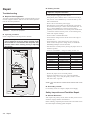
This is a complementary service manual covering instruments with manufacturing numbers exceeding 840684. The principal
differences are to be found in Chapter 7 and in Chapter 8 due to a major redesign of the main PCB.
Do not dispose of the previous edition, identified by the part number, 4822 872 25012, and the publishing date, June 1996.
You may have to refer to it for information on older instruments as well as options not mentioned here.
4822 872 20106
First Edition (May 2003)
No part of this manual may be copied without the express permission of the copyright owner.
All product names are trademarks of their respective companies.
Ó 2003 Pendulum Instruments AB
All rights reserved. Printed in Sweden.
Contents
1
Safety Instructions
2
Performance Check
Introduction . . . . . . . . . . . . . . . . . . . . . . . . . . . . . . . . 6-2
Preparation . . . . . . . . . . . . . . . . . . . . . . . . . . . . . . . . 6-2
Front Panel Controls . . . . . . . . . . . . . . . . . . . . . . . . . 2-2
Short Form Specification Test . . . . . . . . . . . . . . . . . . 2-3
Power Supply . . . . . . . . . . . . . . . . . . . . . . . . . . . . . . 6-2
Input Amplifier . . . . . . . . . . . . . . . . . . . . . . . . . . . . . . 6-3
Rear Input/Output . . . . . . . . . . . . . . . . . . . . . . . . . . . 2-4
Reference Oscillators . . . . . . . . . . . . . . . . . . . . . . . . 6-4
Measuring Functions . . . . . . . . . . . . . . . . . . . . . . . . . 2-4
Other Options . . . . . . . . . . . . . . . . . . . . . . . . . . . . . . 6-6
Disassembly
7
Replacement Parts
Introduction . . . . . . . . . . . . . . . . . . . . . . . . . . . . . . . . 7-2
Removing the Cover . . . . . . . . . . . . . . . . . . . . . . . . . 3-2
Mechanical Parts. . . . . . . . . . . . . . . . . . . . . . . . . . . . 7-3
Reinstalling the Cover . . . . . . . . . . . . . . . . . . . . . . . . 3-2
Main Board . . . . . . . . . . . . . . . . . . . . . . . . . . . . . . . . 7-6
PM9624 (HF Input) . . . . . . . . . . . . . . . . . . . . . . . . . . 3-2
Front Board . . . . . . . . . . . . . . . . . . . . . . . . . . . . . . . 7-12
PM9626B (GPIB Interface) . . . . . . . . . . . . . . . . . . . . 3-3
GPIB Interface (PM9626B) . . . . . . . . . . . . . . . . . . . 7-13
Circuit Descriptions
Block Diagram Description . . . . . . . . . . . . . . . . . . . . 4-2
General . . . . . . . . . . . . . . . . . . . . . . . . . . . . . . . . . . 4-2
8
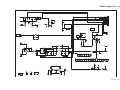
Drawings & Diagrams
How to read the diagrams . . . . . . . . . . . . . . . . . . . . . 8-2
9
Appendix
Hardware Functional Description . . . . . . . . . . . . . . . 4-4
Front Unit . . . . . . . . . . . . . . . . . . . . . . . . . . . . . . . . . 4-4
How to Replace Surface Mounted Devices. . . . . . . . 9-2
Main Board . . . . . . . . . . . . . . . . . . . . . . . . . . . . . . . . 4-5
Glossary . . . . . . . . . . . . . . . . . . . . . . . . . . . . . . . . . . 9-4
Power Supply Switchmode Module . . . . . . . . . . . . . 9-5
Circuit Descriptions . . . . . . . . . . . . . . . . . . . . . . . . . . 9-5
Rear Panel Unit . . . . . . . . . . . . . . . . . . . . . . . . . . . . 4-13
Optional Units . . . . . . . . . . . . . . . . . . . . . . . . . . . . . 4-14
Software Functional Description . . . . . . . . . . . . . . 4-15
Test Routines . . . . . . . . . . . . . . . . . . . . . . . . . . . . . 4-16
5
Calibration Adjustments
Recommended Test Equipment . . . . . . . . . . . . . . . . 2-2
PM9691 or PM9692 (Oven Oscillator) . . . . . . . . . . . 3-3
4
6
General Information . . . . . . . . . . . . . . . . . . . . . . . . . 2-2
Options . . . . . . . . . . . . . . . . . . . . . . . . . . . . . . . . . . . 2-5
3
General Directives. . . . . . . . . . . . . . . . . . . . . . . . . . . 5-9
Repair
Preventive Maintenance. . . . . . . . . . . . . . . . . . . . . . . 5-2
Calibration . . . . . . . . . . . . . . . . . . . . . . . . . . . . . . . . . 5-2
When to Replace the Fan
(PM6685R only ) . . . . . . . . . . . . . . . . . . . . . . . . . . . . 5-3
Troubleshooting . . . . . . . . . . . . . . . . . . . . . . . . . . . . . 5-4
General . . . . . . . . . . . . . . . . . . . . . . . . . . . . . . . . . . . 5-4
Safety Inspection and Test After Repair . . . . . . . . . 5-9
Electrostatic discharge . . . . . . . . . . . . . . . . . . . . . . . 9-3
Repair . . . . . . . . . . . . . . . . . . . . . . . . . . . . . . . . . . . . 9-6
Calibration Adjustments . . . . . . . . . . . . . . . . . . . . . . 9-7
Replacement Parts. . . . . . . . . . . . . . . . . . . . . . . . . . 9-8
PM6685R . . . . . . . . . . . . . . . . . . . . . . . . . . . . . . . . . . 9-12
Introduction . . . . . . . . . . . . . . . . . . . . . . . . . . . . . . . 9-12
Performance Check . . . . . . . . . . . . . . . . . . . . . . . . 9-12
Functional Description. . . . . . . . . . . . . . . . . . . . . . . 9-12
Calibration Adjustments . . . . . . . . . . . . . . . . . . . . . 9-13
Replacement Parts . . . . . . . . . . . . . . . . . . . . . . . . . 9-14
This page is intentionally left blank.
Chapter 1
Safety Instructions
WARNING: These servicing instructions are for use
by qualified personnel only. To reduce the risk of
electric shock, do not perform any servicing other
than that specified in the Operating Manual unless
you are fully qualified to do so.
Authorized service and calibration of this instrument is available
through your Fluke representative. See address at the end of this
manual.
Read this chapter carefully before you check, adjust, or repair an instrument.
Caution and Warning Statements
You will find specific warning and caution statements where necessary throughout the manual.
CAUTION: Indicates where incorrect operating procedures can cause damage to, or destruction of,
equipment or other property.
WARNING: Indicates a potential danger that requires
correct procedures or practices in order to prevent
personal injury.
This Timer/Counter has been designed and tested in accordance with
safety class 1 requirements for Electronic Measuring Apparatus of
IEC (CENELEC) publication EN61010-1, and CSA 22.2
No. 1010-1, and has been supplied in a safe condition.
This manual contains information and warnings that should be followed by the user and the service technician to ensure safe operation
and repair in order to keep the instrument in a safe condition.
WARNING: Opening instrument covers or removing
parts, except those to which access can be gained
by hand, is likely to expose high voltages which
can cause death.
The instrument must be disconnected from all voltage sources before
it is opened. Remember that the capacitors inside the instrument retain their charge even if the instrument has been disconnected from
all voltage sources.
Grounding
This instrument is connected to ground via a sealed three-core power
cable, which must be plugged into socket outlets with protective
ground contacts. No other method of grounding is permitted for this
instrument.
1-2 Safety Instructions,
The ground symbol on the rear panel indicates where the
protective ground lead is connected inside the instrument.
Never remove or loosen this screw.
When the instrument is brought from a cold to a warm environment,
condensation may cause hazardous conditions. Therefore, ensure
that the grounding requirements are strictly met.
Power extension cables must always have a protective ground conductor.
Indicates that the operator should consult the manual.
WARNING: Any interruption of the protective ground
conductor inside or outside the instrument, or disconnection of the protec- tive ground terminal, is
likely to make the instrument dangerous. Do not intentionally disrupt the protective grounding.
Disposal of Hazardous Materials
WARNING: Disposal of lithium batteries requires special attention. Do not expose the batteries to heat
or put them under extensive pressure. These measures may cause the batteries to explode.
A lithium battery is used to power the nonvolatile RAM in this instrument. Our world suffers from pollution, so don’t throw batteries
into your wastebasket. Return used batteries to your supplier or to the
Fluke representative in your country.
Line Voltage
The instrument can be powered by any voltage between 90 and
265 VAC without range switching. This makes it suitable for all nominal line voltages between 100 and 240 V.
n Replacing Components in Primary Circuits
Components that are important for the safety of this instrument may
only be replaced by components obtained from your local Fluke
representative. After exchange of the primary circuits, perform the
safety inspection and tests, as described in Chapter 5, “Repair”.
n Fuses
This instrument is protected by an ordinary 1.6 A slow blow fuse
mounted inside the instrument. NEVER replace this fuse without
first examining the Power Supply Unit.
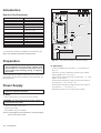
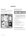
Chapter 2
Performance Check
Preparations
General Information
WARNING: Before turning on the instrument, ensure
that it has been installed in accordance with the Installation Instructions outlined in Chapter 3 of the
Operators Manual.
Power up your instruments at least 20 minutes before beginning the tests to let them reach normal
operating temperature. Failure to do so may result
in certain test steps not meeting equipment specifications.
This performance procedure is intended to:
– Check the instrument’s specification.
– Be used for incoming inspection to determine the acceptability
of newly purchased instruments and recently recalibrated instruments.
– Check the necessity of recalibration after the specified
recalibration intervals.
NOTE: The procedure does not check every facet of the instrument’s calibration; rather, it is concerned primarily
with those parts of the instrument which are essential
for determining the function of the instrument.
It is not necessary to remove the cover of the instrument to perform
this procedure.
If the test is started less than 20 minutes after turning on the instrument, results may be out of specification, due to insufficient
warm-up time.
Front Panel Controls
Power-On Test
At power-on the counter performs an automatic self-test of the following:
–
–
–
–
–
Microprocessor
RAM
ROM
Measuring circuits
Display
If a GPIB interface is installed, the GPIB address is displayed.
If there are any test failures, an error message is shown.
– Turn on the counter and check that all segments light up on the
display and that no error message appears.
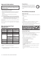
Recommended Test
Equipment
Type of instru ment
LF Synthesizer
Power Splitter
T-piece
Termination
Reference oscillator
HF signal generator
Pulse Generator
Oscilloscope with
probes
BNC cables
Required
Specifications
Square;
Sine up to 10 MHz
50 W
50 W
10 MHz ±0.1 Hz for
standard oscillator
10 MHz ±0.01 Hz for
PM9691 & PM9692
10 MHz ±0.0001 Hz
for PM6685R
0.5 GHz (no presc.)
3.3 GHz (option 10)
125 MHz
350 MHz
Ω
Suggested
Equipment
PM9584/02
PM9585
Fluke counter with
calibrated option
PM9691
Fluke PM6685R or
PM6681R
Fluke 910R or Ce sium Standard
5 to 7 cables *
Fig. 2-1
Text on the display.
Internal Self-Tests
The different built-in test routines invoked by the power-on test can
also be activated from the front panel as follows:
– Enter the Auxiliary Menu by pressing AUX MENU.
– Select the test submenu by pressing DATA ENTRY up or
down.
– Enter the test menu by pressing the ENTER key.
Selections for internal self-tests are:
1 TEST ALL (Test 2 to 5 in sequence)
2 TEST RO (ROM)
3 TEST RA (RAM)
4 TEST LOGIC (Measuring Logic)
5 TEST DISP (Display Test)
– Use DATA ENTRY up/down to select TEST ALL, then press
ENTER.
Table 2-1
Recommended Test Equipment.
*) Two of the cables must have 10 ns difference in delay, for example: 5 ns and 15 ns.
2-2 Performance Check, General Information
– If any fault is detected, an error message appears on the display and the program halts.
– If no faults are detected, the program returns to measuring
mode.
Keyboard Test
The keyboard test verifies that the counter responds when you press
any key. To check the function behind the keys, see the tests further
on in this chapter.
Press the keys as described in the left column and look on the display
for the text, as described in the second column. Some keys change
more text on the display than described here. The display text mentioned here is the text mainly associated with the selected key.
Key(s)
Display
Note
STAND-BY
Display Off
Red LED
beside
the key
On
ON
PRESET
ENTER
EXT REF
Backlight on
DEFAULT?
NO SIGNAL
EXT REF
Default
setting
Input A
FILTER
FILTER
50 W
50 W
(2 times)
SENS
(2 times)
SENS
(2 times)
AUTO
Bar graph:
zzzzzzzz
Bar graph:
zzzzzzzzzz
AUTO TRIG
Other
PRESET
DEFAULT?
ENTER
NO SIGNAL
MEAS TIME
200–3 s
DATA ENTRY
500–3 s
DATA ENTRY 200–3 s
ENTER
DISPLAY HOLD
DISPLAY HOLD
SINGLE
FUNCTION
FUNCTION
FUNCTION
FUNCTION
AUX MENU
MEAS RESTART
PRESET
ENTER
CHECK
NULL
NULL
BLANK DIGITS
(3 times)
MENU
Table 2-2
Default
setting
NO SIGNAL
HOLD
SINGLE
DUTY F A
TOT A MAN
DUTY F A
FREQ A
RECALL
NO SIGNAL
DEFAULT?
NO SIGNAL
10.00000000 6Hz*
NULL
10.00000000 6Hz*
10.00000_ _ _6Hz*
Displays all avail able functions, processes and input
controls. Selected
items are blinking.
Keyboard Test.
Pass
/Fail
NOTE: For the instrument to respond correctly, this test must
be carried out in sequence and you must start with the
preset (power-on) setting.
* The LSD may vary.
** MENU is not disabled by setting DEFAULT; press menu again.
Short Form Specification
Test
Sensitivity and Frequency Range
– Press the PRESET key to set the counter in the default setting.
Then confirm by pressing ENTER.
–
–
–
–
–
–
Turn off AUTO.
Select IMP A = 50 W and maximum sensitivity.
Connect a signal from a HF generator to a BNC power splitter.
Connect the power splitter to your counter and an oscilloscope.
Set input impedance to 50 W on the oscilloscope.
Adjust the amplitude according to the following table. Read
the level on the oscilloscope. The counter should display the
correct frequency.
Frequency
MHz
1
25
50
150
200
250
300
Table 2-3
mVPP
30
30
30
60
90
150
150
Level
mVRMS
10
10
10
20
30
50
50
dBm
–27
–27
–27
–21
–17
-13
-13
Pass/Fail
Input A
Sensitivity of input A at various frequencies.
Reference Oscillators
Default
setting
Start
counting
X-tal oscillators are affected by a number of external conditions,
such as ambient temperature and supply voltage, but they are also affected by aging. Therefore, it is hard to give limits for the allowed
frequency deviation. You must decide the limits depending on your
application, and recalibrate the oscillator accordingly. See the Preventive Maintenance in the Repair chapter, Chapter 5.
Oscillator
Standard
PM9691
PM9692
Rubidium
Table 2-4
Max. tempera ture dependence
±100 Hz
±0.05 Hz
±0.025 Hz
±0.003 Hz
Max. aging
per month
±5 Hz
±0.1 Hz
±0.03 Hz
±0.0005 Hz
Max. aging
per year
±50 Hz
±0.75 Hz
±0.2
±0.002 Hz
Deviation (for PM9691 and PM9692 after a
warm-up period of 48 hours).
To check the accuracy of the oscillator you must have a calibrated
reference signal that is at least five times as stable as the oscillator
that you are testing, see the following table.
– Press the PRESET key, then press the ENTER key to set your
counter in the Default setting.
Performance Check, Short Form Specification Test 2-3
– Connect the reference to input A.
– Check the readout against the accuracy requirements of your
application.
– Press the PRESET key, then press the ENTER key to set your
counter in the Default setting.
n Acceptance Test
As an acceptance test, the following table gives a worst case figure
after a 30 minute warm up time. All deviations that can occur in a
year are added together.
Oscillator
Frequency readout
Standard
10.00000000 MHz
±120 Hz
PM9691
10.00000000 MHz
±1 Hz
10.00000000 MHz
±0.25 Hz
PM9692
Table 2-5
EXT ARM INPUT
Suitable reference
PM9691
Pass
/Fail
PM6685R
PM6681R
n Acceptance Test, PM6685R
To fully test the accuracy of the PM6685R, a reference signal of extremely high stability is needed. Examples of such references are
Cesium Atomic references, or transmitted signals from a nationally
or internationally traceable source, like the GPS satellites.
Recommended Test Equipment
Stability
£ 1x10⁻¹⁰
Select 50 W input impedance.
Apply 10 MHz 500 mVRMS, (1.4 VPP) sine to input A
The counter measures and displays 10 MHz.
Press the AUX MENU key.
Press the DATA ENTRY UP/DOWN keys until the display
shows ‘Ar. Start’, confirm by pressing the ENTER key.
– Press DATA ENTRY UP/DOWN keys until the display shows
‘POS’, confirm by pressing the ENTER key.
Acceptance test for oscillators.
Type
10 MHz reference
–
–
–
–
–
Model
910R with satellite contact during the last 72 hours.
Test Procedure
– Connect the counter to the line power.
– Check that the UNLOCK indicator turns on, and then turns off
again within 6 minutes after connecting line power.
– Connect the 10 MHz reference signal to input A of the counter.
– Select FREQUENCY A measurement.
– Select 2 s measuring time.
– Check that the displayed frequency is 10.00000000 MHz
±0.05 Hz £ 10 minutes after connection to line power.
Rear Input/Output
INT REF Output
– Connect an oscilloscope to the 10 MHz output on the rear of
the counter. Use coaxial cable and 50 W termination.
– The output voltage is sinusoidal and should be above 2.8 VPP.
EXT REF Input
– Press the PRESET key, then press the ENTER key to set your
counter in the Default setting.
– Apply 10 MHz sine to input A equipped with a T-piece and to
Ext Ref input at the rear, terminated with 50 W. Amplitude on
10 MHz signal; 200 mV RMS, (560 mVPP)
– Press the Ext Ref key.
– The display should show 10.00000000 6 Hz ± 5 LSD.
2-4 Performance Check, Rear Input/Output
–
–
–
–
Press the ENTER key once more.
The counter does not measure.
Connect a pulse generator to Ext Arm input.
Settings for pulse generator: single shot pulse, amplitude TTL
= 0 - 2 V PP, and duration = 10 ns.
– Apply one single pulse to Ext Arm input.
– The counter measures once and shows 10 MHz on the display.
Measuring Functions
Preparation for Check of Measuring Function is as follows:
– Connect a 10 MHz sine wave signal with 2.0 V PP amplitude
via a T-piece to Input A.
– Connect a cable from the T-piece to Input E (Ext Arm) at the
rear.
– Select the measuring function as in the ‘Selected Function’ column and check that the counter performs the correct measurement by displaying the result as shown under the “Display”
column in the following table.
Selected Function
PRESET
ENTER
IMP A 50 W
Non AUTO
PER A
RATIO A/E
PWIDTH A
TOT A MAN
DISPLAY HOLD
DISPLAY HOLD
DUTY FACT
AUTO
Table 2-6
Display
DEFAULT?
10 MHz 2)
10 MHz 2)
2)
10 MHz
2)
100 ns
1.0000000
50 ns 1)
Start counting
Stop counting
0.500000 1)
1)
0.500000
Measuring functions check.
1) Value depends on the symmetry of the signal.
2) Exact value depends on the input signal.
Pass/ Fail
Options
Prescaler
This extra HF input (PM9624) is easily recognized by its front panel
connector (Input C, type N).
EX T
RE F
Fig 2-2
Connect the output of the signal generator to the HF
input of the counter.
Required Test Equipment
HF signal generator
Table 2-8
Suggested Specification
3.3 GHz
Test equipment for 3.0 GHz HF input.
– Connect the output of the signal generator to the HF input of
the counter.
– Connect the 10 MHz REFERENCE OUT of the generator to
the REFERENCE IN at the rear panel of the counter.
Setting for the counter after Preset.
– Function = FREQ C.
– EXT REF.
Generate a sine wave in accordance with the following table.
– Verify that the counter counts correctly. (The last digit will be
unstable).
Frequency
MHz
100-300
-2500
-2700
-3000
Table 2-7
Amplitude
mVRMS
dBm
20
–21
10
–27
20
–21
100
–7
Pass/Fail
Sensitivity of the PM9624 HF input.
Performance Check, Options 2-5
This page is intentionally left blank.
2-6 Performance Check, Options
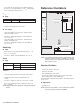
Chapter 3
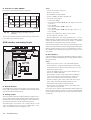
Disassembly
The terms in the following figure are used in all descriptions in this
manual.
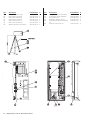
Top
Rear
Left
Fig. 3-1
WARNING: Do not perform any internal service or adjustment of this instrument unless you are qualified
to do so.
Right
Front
WARNING: When you remove the cover you will expose high voltage parts and accessible terminals
which can cause death.
WARNING: Although the power switch is in the off
position, line voltage is present on the printed circuit board. Use extreme caution.
Bottom
Designations used in this manual.
The PM6685 is available with a number of options and accessories.
The labels on the rear panel of the counter identify the options and
accessories included. If there are no labels, the counter contains an
uncompensated crystal oscillator and no options. The following labels exist:
–
–
–
–
Removing the Cover
PM9624 3.0 GHz HF input
PM9691 High-Stability Oven Oscillator
PM9692 Ultra-High-Stability Oven Oscillator
WARNING: Capacitors inside the instrument can hold
their charge even if the instrument has been separated from all voltage sources.
– Make sure the power cord is disconnected from the counter.
– Turn the counter upside down.
– Loosen the two screws (A) at the bottom and the two screws
(B) in the rear feet.
– Grip the front panel and gently push at the rear.
– Pull the counter out of the cover.
PM9626B GPIB Interface
A
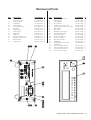
The location of these optional parts is illustrated in Fig.3-2.
A
B
GPIB interface
Optional
oscillator
B
Power
Module
Fig. 3-3
Remove the screws and push the counter out of
the cover.
G1
HF input
Main board
Front panel
Fig. 3-2
Location of the boards in the counter.
Reinstalling the Cover
–
–
–
–
Gently push the counter back into the cover.
Turn it upside down.
Install the two screws (A) at the bottom.
Install the two rear feet with the screws (B) to the rear panel.
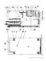
PM9624 (HF Input)
– Disconnect the power cable.
– Remove the cover from the counter.
– Disconnect the cable from the mini-coax connector (A) on the
HF input.
– Press the clips (B) apart and lift the HF input pca straight up
and out.
3-2 Disassembly, Removing the Cover
– When installing the HF input, make sure that the connector
pins fit exactly in the holes in the connector housing (C).
A
PM9691 or PM9692 (Oven
Oscillator)
– Disconnect the power cable.
– Remove the cover of the counter.
– Remove the two screws (A) holding the oscillator to the main
pca from underneath.
– Press the clip (B) gently to the front of the counter and lift the
B
B
oscillator straight up.
– Make sure that jumpers J14 and J15 are set in the correct position.
– When fitting the oscillator, make sure that the connector pins
C
fit exactly in the holes in the connector housing.
A
Fig. 3-6
Removing the HF Input.
PM9626 (GPIB Interface)
– Disconnect the power cable.
– Remove the cover from the counter.
– Loosen the two screws (A) holding the GPIB interface to the
Fig. 3-5
One of the two screws holding the oven oscillator
in place.
rear panel.
– Disconnect the interface cable from P103.
– Move the GPIB interface pca toward the front of the counter
and lift the pca supports out from the “keyholes” (B) on the
main PCA.
A
B
Fig. 3-4
A
B
Loosen the two screws in the rear panel and disengage the board from the keyholes.
Disassembly, PM9626 (GPIB Interface) 3-3
This page is intentionally left blank.
3-4 Disassembly, PM9691 or PM9692 (Oven Oscillator)
Chapter 4
Circuit Descriptions
Block Diagram Description
General
The PM6685 Frequency Counter consists of three main units:
– Front unit
– Main board unit
– Rear panel unit
The following options can be added:
–
–
–
–
–
GPIB interface including analog output (PM9626B)
Prescalers 1.3 GHz (PM9621), 3.0 GHz (PM9624)
Oven-controlled crystal oscillators (PM9691 or PM9692)
Rack mount adapter (PM9622/02)
Battery option (PM9623)
The chassis of the counter consists of a front piece molded in aluminum, an aluminum rear panel, and two profiled aluminum rods that
hold the front and rear panels together. This unit can be slid into the
aluminum cover of the instrument.
The front unit contains all functions needed for the user communication. It is connected to the main board unit with a flat cable, and the
4-2 Block Diagram Description
molded front unit is fixed to the two profiled aluminum rods with
screws.
The main board unit consists of a PCB mounted on two profiled aluminum rods. Most functions, such as the following, are placed on the
main board:
–
–
–
–
Input amplifiers with trigger level circuits
Power supply
Measurement logic
Microcomputer circuitry
Some outputs, such as the trigger levels and probe compensation
view outputs are directly mounted on the main board.
The rear panel unit is of aluminum with a number of mounted connectors. Most of the connectors are soldered directly to the main
board. The rear panel is fixed to the two profiled aluminum rods with
screws.
Optional oscillator
E
External arming
÷2
C
D
A
HF input
INTREF
X2
EXTC
B2
EXTREF
A
A2
GET
10 MHz out
G
U29
Counter
ASIC
External reference
Input Amplifier
Microcomputer
U11
Trigger DAC´s
Local preset
HSI.0
Reset circuit
RESET
Gate LED
I2C
PWM
Display
Analog output
Option 80
AC
Power supply
90-265 V
+5V
+12V
+7V
-5.2V
GPIB option
Keyboard
Fig. 4-1
PM6685 block diagram.
Block Diagram Description
4-3
Hardware Functional Description
Front Unit
Keyboard
LCD Drivers
U13A
Main Board
Keyboard & Display
Board
Latch
U11
U2 02
Dr iver 2
PC F 8576
LC D
1 58 s egm ent s
2:1 M ultiplex
H0-H3
HS1.0
S y nc .
AD0-AD7
CPU
AD0-AD7
SD A
B ac k pl. 0
Bac k pl. 1
P1.0
P1.1
S CL
U 20 1
Dr iv er 1
P C F8 576
U14A
Latch
V0-V7
Fig. 4-2
Front panel LCD drivers.
An LCD and two LEDs are used as indicators. The LCD is used to
show both the measurement result and the state indicators of the instrument setting. The LEDs show standby and gating.
The LCD has 158 segments that are multiplexed with a ratio of 2:1.
Two parallel and synchronized LCD drivers (U201 and U202) are
2
used. They are connected with a serial I C bus to the microcomputer
on the main board. The clock frequency of the drivers is approximately 140 kHz, set by R201. The VLCD pin is connected to GND
on the main board.
The LCD is provided with a backlight, an LED array integrated into
one component. Its current consumption is set by the resistors
R204-R207. The backlight dissipates approximately 1.5 W .
LOCAL/PRESET
SCL
SDA
Fig. 3
Keyboard scanning.
The front panel pushbuttons are connected in a matrix. The scanning
signals H0 to H3 come from the main board. If a push button is
pressed and H0 to H3 is high, one of the output signals V0 to V7 will
be high. The STAND-BY/ON and LOCAL-PRESET buttons are not
part of the scanning but are connected directly to the main board.
The front unit is fixed to the main board unit with three screws. The
electrical connection is made with a 40-lead flat cable to the main
board.
4-4 Hardware Functional Description
selected if the relay is open. Depending on selected attenuation, the
1 MW input impedance is determined by different combinations of
resistors.
Main Board
Introduction
Components not necessary for explaining the function are omitted
from the figures in this chapter. For the complete set of components,
see the circuit diagrams in Chapter 8, Drawings and Diagrams.
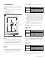
Input Amplifier
The input amplifier has 300 MHz bandwidth and is of the split-band
type. It contains four main stages: the signal adaptation stage, the impedance converter stage, the comparator stage, and the buffer stage.
n Signal Adaptation
This part of the amplifier contains:
– 50 W/1 MW impedance selector
– x1/x11 attenuator
– Voltage limiter
C2
R6
C1
R2
R3-R5
C3
R22-R23
K1
R18
R7-R17
K3
To V olt age
li mi ter
R24R26
R27R28
R19R20
Fig. 4-4
The input capacitance in parallel with 1 MW is 24 pF at x1 attenua tion and 12 pF at x11 attenuation.
The series resistor R1 immediately after the selector serves both as
current limiter together with the voltage limiter (see below) and as
impedance matching resistor. The resistor also improves the Voltage-Standing-Wave-Ratio (VSWR) of the amplifier input.
The x1 attenuator consists of a resistive low-frequency divider,
which reduces the input signal by a factor of 2, and a capacitive
high-frequency divider. The attenuator is formed by the resistors
R22-R23 and R24-R26 in parallel with R27-R28. The capacitive part
is formed by the variable capacitor C2 in parallel with R22-R23, and
the parasitic capacitance across R24-R26.
K2
R1
In x11 attenuation mode (K2 is open and K3 is closed) the same net work as in the x1 case is involved plus the resistors R3 to R5 and R18
to R20.
x1/x11 Attenuator
50 W / 1 MW Impedance Selector
J1
In x1 attenuation mode (K2 is closed and K3 is open) the impedance
is determined by resistor network R22 to R28.
The capacitive attenuator is adjusted via variable capacitor C2 to the
same attenuation value as the resistive attenuator.
The x11 attenuator also consists of a resistive low-frequency divider
and a capacitive high-frequency divider. The resistive part is formed
by R1-R5, and R18-R20 in parallel with 1 MW (the x1 attenuator impedance). The capacitive divider is formed by the variable capacitor
C1 and the parasitic capacitance at the node where R5, R18 and R22
meet.
Resistors R2 and R6 improve the frequency response.
Impedance selector and 1X/11X attenuator.
The 50 W or 1 MW impedance modes are selected by relay K1. 50 W
is selected via the resistors R7 to R17, if the relay is closed. 1 MW is
Input A
Imp.
Att.
Trigger
level Comp I
Trigger
level Comp II
Fig. 4-5
Limiter
Imp.
Conv.
LP
filter
Comparator
Comparator
FlipFlop
Buffer
A
÷2
Buffer
A2
Input amplifier block diagram.
Hardware Functional Description 4-5
and D3 to clamp positive voltage and resistor R36 plus the diodes D2
and D4 to clamp negative voltage. The clamp voltage is approximately ±2.1 V for low frequency signals. At high frequency the
clamp voltage rises to approximately ±2.3 V.
Voltage limiter
+5
R35
n Impedance Converter Stage
D1
The analog signal from the input stage is fed to an amplifier stage
where split-band technique is used to get good frequency response
over a wide range. This means that the high-frequency contents of
the signal are fed to a high-impedance AC-coupled FET transistor
stage Q1. The low-frequency contents are fed to a DC-coupled operational amplifier stage with negative feedback from the output of the
converter stage buffer. The low-frequency path handles frequencies
up to approximately 5 kHz.
D3
From
Attenuator
To Impedance
converter stage
D2
The high-frequency signal is fed to the gate of Q1. The high impedance at the gate is converted to a low impedance at the source. The
source is connected to the base of HF transistor Q2, the summing
point for the two signal paths.
D4
R36
To make the FET work well in its active region within the whole dynamic range, the FET drain is supplied with +7 V via resistor R42.
-5.2
Fig. 4-6
The low-frequency signal is divided by the two resistors R27 and
R28 before it is coupled to the input pin #2 of the operational amplifier U1. The resistors R37 and R38 at the operational amplifier output pin #6 center the output swing, and capacitor C6 stabilizes the
operational amplifier stage.
Voltage limiter.
A voltage limiter that protects the impedance converter against
overvoltage is placed between the attenuator and the impedance converter. The voltage limiter consists of resistor R35 and the diodes D1
+7
+5
R42
Fr om Pro t ec t io n
ci rcu it s
C13
The low-frequency path goes from the operational amplifier to the
base of transistor Q3, the collector of which is connected to the base
+5
R43
Q2
Q1
C20
Q13
R27
R33
C5
R28
R105
-5 . 2
R32
U1
R29R30
Q3
K4
L1
C18C19
Q4
R37
R31
Fig. 4-7
R46
K4
U8
R50
R106
R38
- 5 .2 - 5. 2
Impedance converter.
4-6 Hardware Functional Description
R47
C6
-5 .2
-5 . 2
-5 . 2
Tr i g
L e ve l
+
-
To
Fli p- Fl o p
+
-
The trigger level circuits, which are described later, generate a DC
level in the range of approximately æ1.6 V. This covers a dynamic
range of 6.4 V since the input signal is divided by a factor of 2 before
it reaches the comparator.
of transistor Q2. This point is common to the high and low frequency
paths.
A buffer amplifier with high driving capacity is used to get a linear
output in the 100 W load resistor R106 over a swing of 2 V. This amplifier consists of a driver stage Q2, an output stage Q13, and a cur rent generator Q4.
The counter is provided with adjustable hysteresis, i.e., it is controllable via the front panel or GPIB. The circuitry for setting the hysteresis consists of the resistor network R91 to R96, supplied with +5 V
and –5.2 V. It is connected to the latch enable inputs of the comparator, pin 5 and 7 for Comparator I and pin 17 and 15 for Comparator II.
From the output of this second amplifier stage, the signal is fed back
to the op amp pin 3 via the divider chain R29 to R32. The trimmer po tentiometer R31 sets the gain of the low-frequency path equal to the
high-frequency gain of about 0.9. Capacitor C5 is connected to oper ational amplifier pins #1 and #8 to achieve stable operation. The
trimmer potentiometer R33 between pins #1 and #5 on the opera tional amplifier is used for adjusting the offset voltage of the opera tional amplifier.
The input signal is fed to both comparators, the outputs of which are
used for setting/resetting the Flip-Flop U9.
n Buffer Stage
Before the signal is fed further into the ASIC U29, it has to be
level-shifted by a buffer stage. The negative ECL logic levels
(~ –0.9 V to ~ –1.7 V) from U9 pins 17 and 18, are converted to a
The channel A filter connected to the output of the second amplifier
stage is a 100 kHz low-pass LC filter. It consists of the coil L1 and the
two capacitors C18 and C19 in parallel. The filter is controlled by the
relay K4. The filter output is connected to the input of the comparator
stage.
single-ended signal with CMOS logic levels ( ~ 5 V to ~ 0 V).
The buffer is a differential amplifier consisting of the two transistors
Q32 and Q33 whose bases are fed differentially from the two comparator outputs. Resistor R304 serves as a current generator that is
switched alternately to the two collector resistors R296 and R297.
n Comparator Stage
The comparator stage converts the analog signal from the impedance
converter stage to a square wave. This circuit consists mainly of the
high-speed integrated comparators U8A and U8B plus a separate
trigger level circuit connected to the comparators at pins 9 and 13 via
resistors R87 and R88.
+5
The trigger level circuits generate the trigger voltage levels to the input comparators. The trigger level range is –3.2 V to + 3.2 V with a
maximum resolution of 0.6 mV. The input amplifier attenuation is
B
A
C
R92
D
TP26
R93
TP27
Trigger Level Circuits
R91
E
R94
F
G
+5
T rig ger Lev el I
B
D
+
-
Input si gnal A
U8B
E
U9
F lip F lo p
U9
F
R297
U8A
- 5.2
R87
R296
R96
F
Q32
Q33
To
C ou nter
c ir cu its
Tri gger Lev el II C
+
-
R304
G
R88
- 5.2
Fig. 4-8
Comparator flip-flop and buffer stages.
Hardware Functional Description 4-7
approximately 2 times. The trigger level circuits generate a DC level
that has the same attenuation. This means that the output of this circuit has a range of –1.6 V to +1.6 V with a resolution of maximum
0.3 mV. A dual 8-bit DAC is used. The DACs only generate voltages
between 0 and +1.6 V, but by using a X2 amplifier and an offset shift
of 50%, the voltage range of –1.6 V to +1.6 V is achieved. The supply
voltages to the trigger level circuits are filtered by R and C to prevent
noise originating in the digital circuitry from influencing the trigger
levels. The ground plane under the trigger level circuits is separated
from the rest of the ground plane, and the planes are connected only
at the front of the counter.
The trigger level circuits consist of the following:
– Resistor network R57 to R68 for generating the reference volt ages 0.04 V, 0.22 V, 0.59 V, and 1.6 V.
– Three multiplexers (U3) to select one of the levels. With this
arrangement there is a total trigger level range of
–1.6 V to +1.6 V.
– A double DAC (U4).
– Two current-to-voltage converters U6. These circuits convert
the current at the IOUT pins of the DACs to a voltage. This
signal has a range of 0 V to approximately 1.6 V.
– Two amplifiers, U7, with an amplification of X2, to generate a
signal with a range of 0 V to 3.2 V. Resistors R69 and R70 set
the reference voltage to the amplifier to get the 50 % offset
shift. To get exact voltages, 0.5 % precision resistors are used:
R73-R75, R78-R79 and R80-R82, R85-R86.
– The zero adjust of the trigger levels is done with trimmer potentiometers R69 and R70 connected to the amplifiers in U7.
– Two low-pass filters R87-C29 and R88-C30.
Tr ig ger l ev el C omp I
U6
R73-R74
U7
R75
U3
AD0 - A D8
+5
D0- D7
+ DA CA
1.6V
0 .5 9 V
0 .2 2 V
0 .0 4 V
V RE F R F B
I OUT
V RE F R F B
I OUT
- 5. 2
U6
C om par ator I
C29
R85-R86
R82
U7
R70
- 5. 2
Trigger level circuits.
4-8 Hardware Functional Description
Tr ig ger l evel
C om p I I
R80-R81
+5
Fig. 4-9
R87
R69
A D0 -A D2
U4
R78-R79
R88
C30
C omp ara to r II
tance is 15 Wwhen the resistor is cold but decreases to a few ohms as
it is warmed up by the steady-state current.
Power Supply
n General survey
The AC voltage is rectified in the bridge rectifier D9 and filtered in
C64. C65 suppresses noise from D9. L6 and C82-C83 serve as a filter at the input of U39.
The power supply generates four regulated DC supply voltages to the
counter, as well as some other supply voltages for special purposes.
The power supply block also contains the ON/STANDBY logic.
All inputs and outputs of the power module have HF chokes. The
module is mounted with distance washers on the main board.
The main building block of the power supply is a primary switch
mode power module (U39). The line power AC voltage (90 V to
265 V) is rectified to a DC voltage before it is fed to the power module.
From the module there are three DC voltages outputs. One of those is
regulated (+ 5 V) and the others are unregulated. These voltages will
vary with input line voltage, the current at + 5 V, and at the unregulated voltages. The output marked +15 will be approximately +18 V,
and the output marked –7 will be approximately –8 V. The outputs
are filtered; HF is filtered by C70-C73, and LF is filtered by L7-L9
and C74-C76.
After a line power filter in the power inlet, a fuse of 1.6 AT and an
NTC resistor protect the power supply. The fuse F1 should only blow
if a catastrophic error occurs on the primary side of the power supply.
A short-circuit on the secondary side should not affect the primary
side. To minimize the inrush current to the capacitors at the connection of the power cord, an NTC resistor (R148) is used. The resis-
U40B
K5
+12 V*
Q14
K5
U
-5.2 V
+5
+15
+5 V
J15
R130-R145
D9
-7
U43
R149-R155
Power Module
U39
Filter&Fuse
M ains Inlet
On
Stand by
Q5-Q6
+12 V
U42
U
R156
U41
U21A&Q17
+7 V
*) for ON/STBY control & OCXO
-
Fig. 4-10
U
J31
+
Fan
PM6685R
only
U
Power Supply.
Hardware Functional Description 4-9
n Function
The three DC voltages from the power module are used for
generating the following four supply voltages in the counter:
+5 V
temperature sensor, controls the speed by applying a variable reference voltage to the fan voltage regulator U42.
Counter ASIC
–5.2 V
The main part of the counting logic is integrated in a CMOS ASIC
specially designed for the Fluke MultiFunction Counter series. There
are also analog blocks included in the 100 pin QPF package.
–7 V is used, with regulator U43.
MUX
+12 V
The MUX block is a switchboard for incoming and internal signals
involved in the measuring process. Some signals are divided by 2 to
make it possible to measure higher frequencies. The trigger slope is
controlled by the MUX block as well. A trigger edge detector senses
the presence or absence of comparator pulses and controls the trigger
level DAC’s in the TLDAC block. These functional units form an essential part of the Auto Trigger System.
Regulated +5 V from the power module is used directly.
+15 V is used, with regulator U41.
+7 V
Stabilized +12 V is used, with regulator U21A and Q17.
The following supply voltage is used for a special purpose:
OSC
+12 V*
The oscillator block generates, selects, and distributes the reference
clock for the circuit. The active semiconductors of the standard oscillator are included in this block. The crystal is connected to pins X1
and X2. A TCXO or OCXO is connected to X2 only. An external reference clock is connected to EXTREF. The PWM signal generated at
OTRIM controls the frequency of the reference oscillator after external integration.
This voltage comes directly from the +12 V regulator U41and will be
present as soon as the power cord is connected, regardless of the position of the ON/STANDBY switch. It is used for the ON/STANDBY
control logic and for supplying an optional OCXO in STANDBY to
avoid the long warm-up time otherwise needed to obtain maximum
accuracy.
At stand-by, the four main supply voltages are switched off, but as
described above, some parts of the instrument should not be
diconnected. Therefore the power module will never be switched off.
The PM6685 has consequently only a secondary power switch.
A relay (K5) disconnects the load on the +5 V and –5.2 V at stand-by.
Because the power module must always have a load on the regulated
voltage, seven bleeder resistors R149-R155 are always connected to
+5 V via J15. At stand-by the counter only needs +15 V, so a dummy
load consisting of R130-R145 is connected to the power module by
means of the relay K5 in order to stabilize the operation of the
switchmode converter.
+5 V controls the switching on/off of +12 V and +7 V. When +5 V is
on, Q6 and Q5 will conduct, i.e. +12 V will be on. If there is no +5 V,
Q6 and Q5 will be off, thus blocking the +12 V.
The ON/STANDBY logic controls relay K5, which operates as described above. It is also possible to open the relay by changing the
position of J16.
The ON/STANDBY logic consists of the RS (set-reset) flip-flop
U40B that is controlled by the ON/STANDBY button on the front
panel. Pressing STANDBY will apply a high voltage (+12 V) to the
set input. The inverting output of the flip-flop will be low, disconnecting K5 via Q14. Pressing ON will give a high voltage (+12 V) on
the reset input. The inverting output of the flip-flop will be high,
engaging K5. Inserting the power cord into the power inlet will cause
a pulse on the reset input, via C35. The microcomputer can disable
the ON/STAND-BY button via Q12 and Q7. This is done in remote
mode and during RAM-testing. A high level on the base of Q12 enables STAND-BY, a low level disables it.
The STAND-BY indicator on the front panel is controlled by the
+5 V via Q16. +5 V off lights the STAND-BY LED that is fed by the
uninterruptible +12 V*.
+5 V also indirectly controls the fan in the PM6685R. It is a 12 V DC
fan that operates only if +12 V is on. An NTC resistor, serving as a
4-10 Hardware Functional Description
PG
A built-in pulse generator having the 10 MHz clock as a reference
can generate pulses with controllable duration and repetition rate at
the OUTPUT connector. The level is fixed TTL.
RTC
A real time clock not used at present.
TLDAC
This block contains two 10-bit DAC’s generating the trigger levels
for the input comparators, VOUTA for channel A and VOUTB for
channel B. An external reference voltage is connected to V+REFA
and V+REFB.
HO
The Hold Off block can manipulate the internal measuring signal X
in several ways. One operating mode simulates a low pass filter (normal hold off), another mode is used in burst measurements.
The following blocks (SYNC, STST, CNTS and MCTRL) form the
actual measuring logic in the ASIC. Three types of measurements
can be made in this MEAS block:
Continuous measurements (frequency, ratio and period average).
Not used at present.
Controlled measurements (time interval, period single, pulse width,
frequency, totalize gated, totalize start-stop, and ratio).
Totalize manual.
SYNC
The SYNC block synchronizes the actual measurement with certain
internal or external events like measuring time and arming signals.
STST
The start and/or the stop of the measurements are controlled by this
block. External events can be used to define the exact moments.
RE SET
HODLYX
HODLYY
HOS X
HOS Y
CLOCK
ST OP
ST ART
CLOCK
S TAARM
STOARM
STADLY
STODLY
HOS X
HOS Y
STA ARM
STOA RM
STA DLY
STODLY
GET
TOTSTA
STA
P CL
PGTRIG
GET
Fig. 4-11
Interpolator
CLOCK
STST
MCTRL
OK
FI N1
PGREF
PGTRIG
PGA RM
RTC
TLDAC
RTC
PGREF
I NTB
I NTA
SB
SA
P CL
PG
CY 1
CY 2
S TOP
START
TI ME
MREF
FRE QC
MCLK
P GOUT
OSC
CS RS SS
MPI
+5
VCCG
GNDG
VREFA D
IRES
INTP1
INTP2
INTS1
INTS2
FIN
MTIM E
V+REFA
VOUTA
V-RE FA
V+REFB
VOUTB
V-RE FB
VCCE
GNDE
MCLK
RTC
P GOUT
VCCF
GNDF
ALE
RDN
WRHN
WRLN
CS
A 16
A 17
A 18
A 19
HOLDN
HLDA N
QDM AN
I NT
S 1N
S 2N
S 3N
S4N
S5N
C1
C2
C3
C4
A D0-AD15
RTCX 1
RTCX 2
A LARMN
V BAT
+5
PG
X1
X2
V+REFO
OTRIM
V-REFO
E XTREF
MTCXO
INTREF
OUTMUX
MPCLK
P H1
P H2
V CCB
GNDB
VCCC
GNDC
GNDA
V CCA
VCCX
TOTSTA
STA
R1
R2
L1
L2
DMA R
TI ME
M RE F
F RE QC
M CLK
P GARM
R1
R2
L1
L2
I
I F Na
F Nb
OK a
OKb
HODLYX
HODLYY
XH
YH
XH
YH
CNTS
DMA BR
X
Y
X
Y
SYNC
I
I F NA
I F NB
I F NC
F ND
OKA
OKB
OK C
OKD
HO
GA TEO
MUX
A2
A
SR
B
B2
EXTC
P
BURST
TRA
TRB
V CCO
GNDD1
GNDD2
GNDD3
GNDD4
Counter ASIC, block diagram.
CNTS
Two 32-bit binary counters count external events or keep track of the
time.
Interpolator
This block is not used at present.
MCTRL
The different events in the measurement cycle of the ASIC are timed
by this block.
MPI
This is the microprocessor interface block. The bus width is 16 bits,
AD0 to AD15. Interrupts to the microprocessor are generated at INT.
GET
The GET signal from an optional GPIB interface can control the start
of a measurement.
n External Interpolator
The X-POLATOR unit is connected directly to the internal
interpolator in the ASIC. It is used for increasing the time resolution
beyond the limits set by the reference clock period of 100 ns. An er ror pulse is generated in the SYNC block. Its width is determined by
the difference between an external event on an input channel and the
next clock pulse. This pulse controls a current generator charging a
capacitor. When the pulse has expired the voltage across the capaci tor is A/D converted and the value is added to the result. There are
two interpolators, one for the start event and one for the stop event.
They are calibrated over the possible error pulse range to allow for
any aberrations from the theoretical linear behavior.
Oscillator Circuits
n CPU Oscillator
The microcontroller U11 is clocked at 12 MHz. The crystal B1 is
connected to the XTAL inputs of the microcontroller.
n Reference Oscillators
A 10 MHz crystal oscillator is used as the reference for the measuring logic. If a stable external 10 MHz reference is available, it can be
connected to REF IN on the rear panel and selected by means of the
EXT REF button on the front panel.
In addition to the standard crystal oscillator there are two optional
oven-controlled crystal oscillators (OCXO) to choose from.
Standard
The uncompensated standard oscillator consists of the crystal B2,
C109, C113-C115, R209 and R211. C115 is used for manual adjustment of the frequency when the calibration tolerance has been exceeded. The active circuitry is built into the ASIC U29 and is accessible via the pins marked X1 and X2.
OCXO
If one of the OCXOs is mounted, the standard oscillator has to be inactivated by moving the jumpers J23 and J25 to their alternative position. These oscillators are connected to J24 and are self-contained
Hardware Functional Description
4-11
units with facilities for coarse and fine adjustment. They are fixed to
the main PCB with two screws. The output signal is AC-coupled to
the X2 pin on U29 via C107.
n Keyboard Scanning
U13A
Main Board
External
Keyboard & Display
Board
Latch
U11
This input consists of an AC-coupled line receiver with Schmitt trigger function (U28) and is protected against excessive voltage
excursions by a resistor-diode network. The output signal from U28
has CMOS logic levels and is connected to the EXTREF pin on the
counter ASIC U29.
AD0-AD7
H0-H3
AD0-AD7
HS1.0
P1.0
P1.1
CPU
Logic
U14A
Latch
V0-V7
n Microcomputer Circuits
Microcontroller
The microcomputer circuitry consists mainly of the microcontroller
U11, an Intel 16-bit CMOS 80C196, RAM (U22A), and EPROM
(U23A). The microcontroller is clocked at 12MHz. The data and address lines AD0 to AD15 are shared by means of multiplexing.
Therefore the addresses are stored in the latches U16A and U17A.
The ALE signal (Address Latch Enable) enables the latches.
UVEPROM
The main program is stored in U23A that is mounted in an IC socket,
making it easy to update and customize the instrument firmware by
changing the EPROM.
EEPROM
Front panel settings, GPIB address and certain other data that are not
changed frequently, e.g. information in the Protected User Data
Area, are stored in U12A which does not need battery backup.
Reset Circuit
A special reset circuit, the power supply supervisor U10, is included
in the design. If the +5 V supply line becomes lower than 4.5 V, the
reset output pin 5 goes low and the microcontroller will start over.
The length of the reset pulse is set by C88; 2.2 µF gives a pulse of approximately 30 ms. U10 also controls the reset pulse during
power-up so that the microcontroller will be initiated correctly.
LOCAL/PRESET
SCL
SDA
Fig. 4-13
Keyboard scanning.
The keyboard scanning is done in two modes. The first mode is active as long as no button has been detected as depressed. Then all outputs of U13A are set high, and the latch U14A is read. If no button
has been depressed, all outputs are low. This check is done at every
timer interrupt in the microcontroller, every 25 ms. If a button is
depressed, one of the output bits is high. When this event is detected,
mode two is entered. The outputs of U13A must be set high one after
the other to find the specific button. When found, only this button
will be checked, so other simultaneously depressed buttons will not
be recognized. The depressed button must stay down for several
timer interrupts before action is taken. After the button has been recognized, the timer interrupt SW will be waiting for the button to be
released. The button must be released for several timer interrupts before the keyboard scanning returns to mode 1. Then the search for
other activated buttons can be resumed.
The following three buttons are not scanned in this way:
– The ON button is connected to the ON/STANDBY logic in the
power supply.
CPU
Latch
RAM
UV
EPROM
OMBus
Address
Keyboard
Latch
Address & Data Bus
2
I C Bus
rd
GPIB
Fig. 4-12
Microcomputer circuits, block diagram.
4-12 Hardware Functional Description
EE
PROM
Counter
ASIC
LCD
Drivers
LCD
– The STAND-BY button is connected to the ON/STANDBY
logic in the power supply.
– The LOCAL/PRESET button is connected directly to input pin
24 on the microcontroller U11. Pressing this button sends an
interrupt to a special handler in the SW.
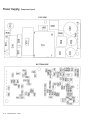
Rear Panel Unit
The rear panel contains the following connectors
INPUTS:
– External reference input D - REF IN (BNC)
– External arming input E - EXT ARM (BNC)
– Power supply inlet including EMI filter
OUTPUTS:
– Internal reference output G - 10 MHz OUT (BNC)
If a GPIB interface is installed in the device, it is mounted on the rear
panel and connected to the main board with a flat cable.
Besides the normal standard GPIB connector, this optional unit also
has a BNC connector capable of outputting an analog representation
of any three consecutive digits on the display.
There is also a 6 SPST DIP switch on this unit for setting the default
GPIB address.
90 V - 26 5V
A NA L O G O U T
P
P
P
P
ON
OF F
M9 6 2 1
M9 6 2 3
M9 6 2 4
M9 6 2 5
16 8 4 2 1
A DDR E S S
P
P
P
P
I E E E 4 88 / IE C 62 5 INT ER F ACE
S H 1, AH1 , T 5 , L4 , SR 1 ,
R L1 , D C1 , DT 1, E 2
M9 62 6
M9 67 8
M9 69 0
M9 69 1
P M9 6 28 / 85
P M9 6 9 7
_ _ _ _ _ __
_ _ _ _ _ __
1 0 M Hz O U T
G
Fig. 4-14
RE F I N
D
EXT SUPPLY
12-24V DC
- I NT - S T B Y
B AT T E R Y
- EX T /L I NE
P O WE R
P R I MA RY F U S E
1 . 6 AT
I N S ID E
E XT AR M
E
Rear panel.
Hardware Functional Description
4-13
n Analog Out
Optional Units
GPIB Interface Including Analog Output
n GPIB, PM9626B
Basic board
IC101/106/117
The result on the display can be converted to an analog signal by
means of a pulse-width-modulated (PWM) signal from the microprocessor. The signal is filtered, attenuated, offset-adjusted, integrated and buffered by IC103 and supporting passive components to
give an analog DC level between 0 and 4.98 V with a resolution of
20 mV. The analog output has a separate analog ground connected to
the cabinet.
HF Input
IC107/108
IC109/
110
A0-15
IC114/115
IC113
GPIB
connector
AD0-15
IC111/
112
IC116 +5V
You can add an optional prescaler. This HF input is mounted on the
main board, to the right of the input amplifier. It is connected to J19
where there are three pins reserved for ID coding. Preparations have
thus been made for other prescalers with different prescaling factors.
n Prescaler 3.0 GHz, PM9624
This prescaler cannot be repaired at a local workshop. It must be sent
to the factory for repair.
The prescaler consists of the following parts:
Fig. 4-15
Limiter
– The limiter consists of a 6 dB attenuator and a PIN diode at -
GPIB interface.
The GPIB interface controls the communication between the internal
microprocessor and the external GPIB bus. A 32K extension of the
ROM and RAM is placed on the interface board. An analog output is
also included. The PCB is connected to J18 on the main board with a
ribbon cable and fixed to the rear panel with two screws. Two metal
studs at the rear edge of the PCB are inserted in slots on the main
board in order to relieve mechanical stress.
The GPIB control circuit, IC113, communicates with the external
GPIB bus via the bidirectional bus drivers IC114 and IC115. IC113 is
controlled from the microprocessor by writing and reading in the internal control registers. If IC113 has a message for the microprocessor, it uses the GPIB interrupt signal. The address switch setting is
read by the microprocessor via IC116.
A 32K extension of both ROM (IC109 and IC110) and RAM (IC111
and IC112) is placed on the interface board. The circuit board is prepared for a 16-bit extension, but only 8 bits are used. IC110 (ROM),
IC112 (RAM) and R118 are not mounted. IC107, IC108 are address
latches and IC101, IC106 and IC117 use the latched address to generate chip select and chip enable signals for internal use on the GPIB
board.
-5.2V
Zero
+7V
IC103
IC103
PWM
Full scale
Fig. 4-16
Analog output.
4-14 Hardware Functional Description
Analog
Out
tenuator to achieve constant input amplitude to the amplifiers.
Amplifier
– Five amplifier stages are divided into three blocks. One block
consists of one amplifier. Two blocks consist of two amplifiers
each and an AGC control.
Automatic Gain Control (AGC)
– Helps the amplifiers retain a constant output amplitude.
Dividers
– Two dividers divide the input signal frequency by 16.
Detector
– Detects whether the level of the input signal is high enough to
ensure correct measurement and, if not, blocks the output sig nal from the prescaler.
Positive Voltage Regulator
– Supplies a well-regulated voltage to the HF amplifiers.
Software Functional Description
General
The PM 6685 software is divided into two main modules: the GPIB
and DEVICE modules. The GPIB fully implements the Message Exchange protocol as described in the IEEE 488.2 - 1987 standard.
The DEVICE module is a real-time measurement executive that can
be interrupted to do other tasks, such as handling the keyboard, performing bus commands etc.
The basic structure of the main module is as follows:
main PM6685()
{
Initialize();
while (TRUE)
{
if (BREAKFLAG_KEYBOARD)
{
HandleKeyboard();
}
if (BREAKFLAG_PRESET)
{
PresetDevice();
}
if (BREAKFLAG_GPIBCOMMAND)
{
ExecuteGpibCommands();
}
if (BREAKFLAG_RESTART)
{
RestartMeasurement();
}
while (not any BREAKFLAG)
{
Measure( );
}
}
}
All break flags are set by interrupt-driven events, either from external functions (the GPIB interface) or from internal functions (timers
etc.).
The Initialize procedure does all necessary initialization at power
up. It also does the power up tests. See Power-On test in chapter 2.
The Handlekeyboard procedure controls all user input/output via
the front panel, except displaying the measurement results.
The PresetDevice procedure reprograms the complete device when
the PRESET key has been pressed (in local mode). It aborts pending
measurements.
The ExecuteGpibCommands procedure executes GPIB commands
and, if a query is received, it starts the response formatter and sends
the requested data to the GPIB interface. If the display is switched
on, the results are also displayed.
The RestartMeasurement procedure aborts pending measurements; the measure loop will later continue to measure. This is
mainly used when the RESTART key is pressed.
The Measure procedure is the measurement control loop that is used
in local mode. It sends its result to the display.
The ParseGpibInputData procedure parses the GPIB messages
found in the input buffer and sends executable statements to the
ExeceuteGpibCommands procedure. The input of data to the input
buffer from the external GPIB interface is fully controlled in interrupts. These interrupts are always enabled so the new data bytes can
be stored in the input buffer while parsing commands. This
ParseGpibInputDat is also executed in interrupt.
Software Functional Description
4-15
Test Routines
Test Routines via AUX MENU Key
The test routines are the routines accessible via the AUX MENU key.
Refer to the PM6685 Operators Manual.
Power-On Tests
At power-on some tests are automatically performed. If any of these
tests fails, an error message is displayed and the instrument is halted.
Pressing the LOCAL/PRESET key makes the device continue independently of the detected error, but without performing the next tests
in the start-up sequence.The following tests/actions are performed:
–
–
–
–
–
–
–
–
–
–
–
–
–
–
–
Write 001 to internal test pins
Pulse all microcomputer i/o ports twice
Write 0.1 on display
Write 0.1.2. on display and 010 on test pins
Test mC internal RAM ( error = Err mC & halt)
Write 0.1.2.3 to display and 011 on test pins
Test mC timer ( error = Err mC & halt)
Write 0.1.2.3.4. on display and 100 on test pins
Test main board RAM ( error = Err ra. & halt )
Write 0.1.2.3.4.5. to display and 101 to test pins
Test ASIC ( error = Err. 5xx & halt)
Write 110 on test pins
Check display (light all segments for 2 s)
Clear Display
Perform GPIB RAM test if GPIB is installed
(error = Err ra. & halt)
– Write 111 on test pins ( final value)
– Clear display and start normal measurement procedure
4-16 Software Functional Description
Chapter 5
Repair
Preventive Maintenance
Calibration
– The stability indicated for the oscillators is valid within a temperature range of 0 to +50 °C, with a reference temperature of
+23 °C. If the timer/counter is used in a room temperature of
20 to 30 °C, the temperature stability of an OCXO will be increased by a factor of 3.
To maintain the performance of your counter we recommend that
you calibrate your instrument every year, or more often, if greater
time base accuracy is required. Calibration should be performed with
traceable references and instruments at a certified calibration laboratory. Contact your local Fluke representative for calibration.
– The temperature stability indicated for the standard oscillator is
mainly dependent on the ambient temperature. When the counter is operating there is always an internal temperature increase
that will influence the oscillator.
To know the present status of your instrument, test your timer/counter from time to time. The test can be made according to the information in Chapter 2, Performance Check.
n Recalibration intervals
Oscillators
The Mean Time Between ReCalibration, MTBRC, is defined as:
The frequency of the reference crystal oscillator is the main parameter affecting accuracy in a counter. The frequency is affected by external conditions like the ambient temperature and supply voltage,
but also by aging. When recalibrating, the reference crystal oscillator
is compensated only for deviation in frequency due to aging.
MTBRC =
MTBRC can be calculated when the total acceptable error and the
oscillator specifications are known.
The total acceptable error is defined as:
n Some important points:
– The high stability oscillators have been built into an oven in
( Acceptable error) =
order to keep the oscillator temperature as stable as possible.
Continuous operation is also important for stability. After a
power interruption, the oscillator restarts at a slightly different
frequency. It will then, as time goes on, age at an equal rate.
Model
Total uncertainty, for operating temperature
0 °C to 50 °C, at 2 s (95%) confidence interval:
1
3
1
2
month after calibration
months after calibration
year after calibration
years after calibration
Typical total uncertainty, for operating
temperature 20°C to 26°C, at 2 s (95%) confidence interval:
- 1 month after calibration
- 3 months after calibration
- 1 year after calibration
- 2 years after calibration
*
st
After 1
Table 5-1
(Deviation of reference frequency)
(Nominal reference frequency)
PM6685
Option: Standard
Timebase type: UCXO
-
( Acceptable error) − (Temperature stability)
( Aging)
st
year of operation. For 1
PM6685R
PM9692
OCXO
Rubidium
x 10
-5
x 10
-5
x 10
-5
x 10
-5
<
<
<
<
3 x 10
-8
4 x 10
-7
1 x 10
-7
2 x 10
-8
<
<
<
<
8 x 10
-8
1.2 x 10
-8
2.5 x 10
-8
5 x 10
4 x 10
-6
4 x 10
-6
7 x 10
-5
1.2 x 10
-6
<
<
<
<
3 x 10
-8
4 x 10
-7
1 x 10
-7
2 x 10
-8
<
<
<
<
8 x 10
-5
1.2 x 10
-8
2.5 x 10
-8
5 x 10
<
<
<
<
1.2
1.2
1.2
1.5
<
<
<
<
year add: < 3 x 10
Stability of timebase oscillators.
5-2 Preventive Maintenance
PM9691
OCXO
-10
-9
<
<
<
<
4 x 10
-10
4 x 10
-10 *
4 x 10
-10 *
6 x 10
-10
-9
<
<
<
<
1 x 10
-10
2 x 10
-10 *
2.5 x 10
-10 *
5 x 10
-10
Example:
– A user can accept a maximum of 3 Hz deviation on the
10 MHz frequency of the oscillator. This results in:
3
( Acceptable error) =
= 3 × 10⁻⁷
10 × 106
The aging and temperature factors can be selected from the table on
page 5-2.
The value of the aging factor is correctly selected from the table
when the calculation of MTBRC results in 1 to 30 days (use /24h), 1
to 12 months (use /month) or over 1 year (use /year) (not, e.g., 43
days or 17 months or 0.8 years).
Example:
– The user has the same requirements as in the example above.
The counter has a PM9691 oscillator.
– Look up information about PM9691 in the table on page 5-2.
The results will be the following:
Relative Frequency deviation caused by:
– Ambient temperature deviation
– Aging/year: Less than 1.5 * 10–7
– Use the MTBRC formula with the above values. This gives a
MTBRC of maximum:
3 × 10⁻⁷ − 3 × 10−8
= 18
. year
15
. × 10−7
NOTE: When recalibrating, the reference crystal oscillator will be
compensated only for frequency deviation caused by aging.
When to Replace the Fan
(PM6685R only )
To maintain the high reliability of a counter used in
around-the-clock’ applications, you must replace the fan every second year. For part time and low ambient temperature use, you can extend this service interval to 6-10 years or more. Additional information can be found in Chapter 9, Appendix.
(within 0 to 50 °C; reference point at 23 °C): Less than
–8
3 * 10
Preventive Maintenance
5-3
Troubleshooting
General
Required Test Equipment
Quick Troubleshooting
To test the instrument properly using this manual, you will need the
equipment listed below. The list contains specifications for the critical parameters.
The PM6685 is a highly integrated Frequency counter with dedicated
LSI counter circuits and microcontrollers that control the complete
units. The microcontroller can help you locate faulty parts by running test programs and generating stable signal patterns on t
he bus. If the microcontroller does not work or the fault is in a part of
the counter that cannot be accessed by the microcontroller, traditional troubleshooting must be performed.
Table 5-3
Where to Start
After reading the safety instructions, continue with this chapter for
troubleshooting and repair instructions. When you have fixed the instrument, always do the Safety Inspection and Test after Repair, as
described later in this Chapter. Then do the checks in Chapter 2, Performance Check. Recalibrate if required by following the adjustment
instructions in chapter 6, Calibration Adjustments.
Logic Levels
The PM6685 contains logic of four families. The levels for these
families are listed in the following table.
Positive
ECL
+5 V
0V
Negative
ECL
-5.2 V
0V
High, VIH
Low, VIL
Output voltage
High, VOH
>+3.9 V
<+3.5 V
>-1.1 V
<-1.5 V
Low, VOL
Bias ref. voltage, V BB
<+3.3 V
+3.7 V
Supply voltage
Signal ground
CMOS
+5 V
0V
TTL
+5 V
0V
Input voltage
Table 5-2
Type
DMM
Oscilloscope
Signal generator
Power supply
BNC-BNC 50 W cables
>+4 V >+2 V
<+1 V <+0.8 V
Performance
3.5 digits
300 MHz 2-channel
3300 MHz
12 V/2 A
RG-58
Required test equipment.
PROM Identification
There are two different PROMs in the PM6685, one on the main
PCB containing the instrument firmware, the other on the optional
GPIB board, containing the interface bus firmware.
They have labels with version designation of the traditional form
Vx.yz, where x, y, and z are digits. The last digit can be followed by a
single letter. The version numbers do not have to coincide, except for
the last letter. So the combination Vr.stE and Vu.vwE is valid,
whereas Vr.stE and Vu.vwF is not.
Operating Conditions
Power voltage must be in the range of 90 to 260 VAC.
Introduction
GPIB(Level 10)
>+4 V
>-1 V
>+4.9 V >+2.7 V
INPUT AMPLIFIER(Level 9)
<-1.7 V <+0.05 V <+0.4 V
-1.3 V
-
D/A CONVERTE RS (Level 8)
MEASURI NG LOGIC(Level7)
Logic levels.
KEY BOARD (Level6)
INTE RNAL CONTROLS IGNALS & DIS PLA Y (Level 5)
M ICROCO MPUT ER KERNEL (Level 4)
M ICROCONTROLLER (Level 3)
OSCILLATOR(Level 2)
POWE RSUPPLY (Level 1)
Fig. 5-1
Functional levels.
The troubleshooting strategy for the PM6685 is an integrated part of
the overall service strategy for the instrument. This instrument is hi-
5-4 Troubleshooting
erarchically designed in different levels, and troubleshooting can be
performed in any design level if the lower levels are OK. It is, there fore, important to disconnect all options at the beginning of the trou bleshooting procedure.
To verify the Power Module proceed as follows:
– If the primary fuse is broken, there is a short circuit in the
–
Power Supply
–
J3
J4
Fuse
J9
–
–
J10
1
5
Po wer
Mo du l e
+5V adjust
TP20, -5.2
TP23, +5
TP21,+12V
J21
Load
TP15, +5
Disconnected
TP17, -7
14
Test Pins
(GND) and TP15 (+5 V)
(GND) and TP16 (+15 V)
Resistance
»10 W
»1.5 kW
(GND) and TP17 (–7 V)
»270 W
Table 5-5
J16
Connected
6
TP22, +7
primary circuits. Use a DMM and try to locate the fault by
resistance measurements.
Disconnect L6 and check the resistance between pin 1 and
pins 4 and 5 on the power module. The DMM should not
show a short circuit. Put L6 back.
Check that the DC voltage between pin 1 and pins 4 and 5
on the power module is about Ö2 times the input
AC-voltage. If not, use traditional troubleshooting techniques to locate the fault.
Remove the power cable from the counter.
Measure the resistances according to the table below.
Output resistances.
– If one of the above-mentioned measurements shows 0 W,
remove L7, L8, and L9 and use conventional troubleshooting techniques to isolate the fault.
– Measure the resistances according to the table below.
Test Pins
10, 11 and 13, 14
8 and 9
6 and 7
J15
Table 5-6
TP16, +15
Resistance
»150 W
»1.5 kW
»270 W
Output resistances.
If the resistances deviate considerably from the values in the table,
the complete power module must be replaced.
Fig. 5-2
Test points and trimmers for the power supply.
Connect the counter to line power.
– Set the counter to STAND-BY mode.
– Check that the voltage between J9 and J10 is in the range of
90 to 260 VAC, (see Fig. 5-2).
– Check that the input voltage to the power module, U39 be-
tween pin 1 and pins 4 and 5 on the bottom side of the PCA, is
120 to 375 VDC.
– Move the jumper J16 to the DISCONNECT position.
– Check the “STAND BY” voltages after the power module,
U39. Use for instance the screen around the input amplifier as
ground connection. There are also a number of ground pads on
the PCB available for this purpose.
Test Points
TP15
TP16
TP17
Voltage
+5.10 V ± 10 mV*
+14.8 V to +21 V
–12.5 V to –7.5 V
TP21
+12 V ± 0.5 V
Table 5-4
– Move jumper J16 to the CONNect position.
– Connect the power cable to the counter.
– Switch the counter ON.
– Check the “POWER ON” voltages.
Test Points
TP23
TP20
TP22
Table 5-7
Voltage
+5.06 V ± 30 mV*
–5.2 V ± 50 mV
+7 V ± 100 mV
Power-on voltages.
*NOTE: If the +5 V voltage is outside the specification, all
other levels will be wrong, since they are based on the
+5 V level.
If you find any fault, continue with traditional troubleshooting techniques and replace defective circuits. Also refer to Power Supply in
Chapter 4, Circuit Descriptions.
Standby voltages.
*NOTE: If this voltage does not meet the above-mentioned
spec, and if it is not possible to adjust it, the output
resistances of the module must be checked.
Troubleshooting
5-5
Oscillator
– Check that the RESET circuit U10 works properly by moving
B2
1
U23
C11
14
J27
Optio
Stand
U22
Optional OCXO
Coarse adjust
Fine adjust
U17
61
U16
U11
27
1
B1
44
10
U23
1
B2
31
U13
81
51
1
U29
J23 J25
Optional oscillator
Standard oscillator
C115
Fig. 5-3
Trimmers for the reference frequency oscillators.
n Standard Oscillator
– Be sure the jumpers J23 and J25 are in the STD position, (see
Fig. 5-4).
– Check that 10 MHz is present at U29, pin 42.
– Check that 10 MHz is present at the rear panel connector
10 MHz OUT (J27).
If you find any fault, continue with traditional troubleshooting techniques and replace defective circuits. Also refer to Chapter 4, Circuit
Descriptions, Oscillator Circuits.
n OCXO, PM9691 or PM9692
This test can be carried out only if the counter is equipped with one of
the optional oscillators, PM9691 or PM9692.
– Be sure the jumpers J23 and J25 are in the OPT position, (see
Fig. 5-4).
– Check that 10 MHz is present at U29, pin 42.
– Check that 10 MHz is present at the rear panel connector
10 MHz OUT (J27).
These oscillators cannot be repaired in a local workshop. They must
be sent to the factory for repair.
Microcontroller
– Check that 6 MHz is present at U11, pin 65 (see Fig.5-3).
5-6 Troubleshooting
Test points and jumpers for checking the
microcontroller.
the RESET jumper J29 temporarily to the ON position.
If the CPU is not running, check the state of the pins J11-J13. See table below.
Display
Fig 5-4
J29
U14
J30
J13
J14
J24
J11
J12
r
e
0.1
JP11, J12, Message
J13
0, 0, 1 -
0.1.2
0, 1, 0
Err UC
0.1.2.3
0, 1, 1
Err UC
0.1.2.3.4
0.1.2.3.4.5
All segments
1, 0, 0
1, 0, 1
1, 1, 0
Err rA
Err ASIC
1, 1, 1
Err rA
Table 5-8
Error
mC I/O port
error
mC internal
RAM error
mC timer error
RAM error
ASIC error
GPIB RAM
error
Test OK
Action
Replace U11
Replace U11
Replace U11
Replace U22
Replace U29
Replace U111 on
GPIB board
Start-up test.
If you find any fault, continue with traditional troubleshooting techniques and replace defective circuits. Also refer to Chapter 4, Circuit
Descriptions.
NOTE: Check that activity is going on at U11 pin 62 (ALE), pin
61 (RD), pin 63 (INST), and pin 43 (READY). These
pins should not be stuck HIGH or LOW.
– If one or more bits on the AD-bus are corrupt, the
microcontroller (mC) often reads the same instructions repeatedly. When the mC discovers an invalid OP code, it will
RESET itself and start from the beginning again. The mC
sets the RESET input low when it resets itself. This can be
discovered at the RESET input of U11, (pin 16). If +5 V to
U10 is OK, this could be the cause of trouble.
Input Amplifier
n A Input Check
DC levels
– Switch on the counter.
– Press LOCAL/PRESET and ENTER.
– Deselect AUTO and set the sensitivity to 1 Vrms.
– Measure the DC voltages according to Fig. 5-5. Use the DMM
-1.7V -0.9V
with a 10 kW resistor in series with the test cable.
U9
AC levels
TP27, -1.4V
– Connect a 1000 Hz sine wave signal with an amplitude of
1 Vpp to Input A.
TP10
– Measure the AC-levels according to Fig. 5-5. Use the oscilloscope and a 10 MW probe.
TP26, -1.4V
R91
U8
If you find any fault, continue with traditional troubleshooting techniques and replace defective circuits. Also refer to Input Amplifiers
A and B in Chapter 4, Circuit Descriptions.
TP11
R33 R31
0V
0.6Vpp
U1
0V
0.3Vpp
Q4
Q13
1.5V
0.6Vpp
Q3
Q1
-3V
0.8V
4.3V
0.8V
7V
0.4V
-2.3V
D4
2V
D2
D1
-2V
D3
Q2
R23
C2
0.6Vpp
R22
1Vpp
C1
Fig. 5-5
Typical voltages, input amplifier.
Troubleshooting
5-7
n Prescaler 3.0 GHz, PM9624
Setup
See Chapter 2, Performance Check, for verification.
–
–
–
–
–
Sensitivity
-10 dBm
-20 dBm
-30 dBm
-40 dBm
-50 dBm
0
Fig. 5-6
1 GHz
2.5 GHz
Frequency
2 GHz
Specified and typical sensitivity of input C
(PM9624).
This prescaler cannot be repaired in a local workshop. It must be sent
to your Fluke representative for repair.
GPIB Interface and Analog Output
BU102
BU103
U114
Zero
U115
U116
GPIB
U109
U111
U108
Full Scale
U107
BU101
U113
U103
Press PRESET and then ENTER.
Connect a DMM to the BNC output BU102.
Activate the analog output.
– Select AUX MENU.
– Press DATA ENTRY p/q until the display reads ANALOG OUT.
– Press ENTER
– Press DATA ENTRY p/q to select ON.
– Press ENTER.
-3
– Press DATA ENTRY p/q until the display reads 1.0 V.
– Press ENTER.
– Connect a LF synthesizer to Input A on the counter.
– Set the synthesizer to 500 Hz, 1 VPP
– Read the DMM result. The voltage should be 2.49 V ± 35 mV.
Minor deviations can depend on the settings of the trimmer potentiometers for ZERO and FULL SCALE. See Chapter 6, Calibration
Adjustments, for a decription of the procedure to follow.
Large deviations indicate a fault. Trace the signal through the integration chain with traditional troubleshooting techniques and replace
defective circuits. The duty cycle at U101:1 should be 50 %. Also refer to GPIB Interface Including Analog Output in Chapter 4, Circuit
Descriptions.
n Bus Interface
A simple method to check the most fundamental functions of the interface is to send the standardized query message *IDN? and check
the response string.
Setup
– Make sure you have access to a PC with GPIB capability.
– Check that there is a program installed that can send simple
commands entered via the keyboard and that can receive and
display the response strings.
means of a standard GPIB cable.
U117
Component layout, GPIB interface.
n General Remark
If the GPIB board is suspected to be faulty, be sure the basic instrument is OK by performing a few functional checks after the ribbon
cable has been disconnected from J18.
n Analog Output
The microcontroller generates a PWM signal that is applied to pin 1
on U101. The frequency is approximately 20 Hz, but the duty cycle is
dependent on several factors like the frequency of the measured signal, the measurement time, and the selected scaling factor.
The PWM signal is converted to a DC voltage between 0 V and
4.98 V by integration, first in a passive RC network (R101, C103,
R102, C102 and then in an active integrator U103.
5-8 Troubleshooting
Switch on the counter.
– Connect the GPIB connectors of the counter and the PC by
U106 U101
Fig. 5-7
Connect the counter to line power.
– Set the address switches on the counter (the five rightmost
ones seen from the rear) so that their binary weight corresponds to the wanted decimal value between 0 and 30.
– Send the command *IDN? to the counter and observe the re sponse string. See the programming manual for more
information on the response format and contents.
– You can also try the command * OPT? to get a listing of installed options (except OCXO).
If you find a fault, continue with traditional troubleshooting techniques and replace defective circuits. Try to exercise the address/data
bus by writing small program loops. Look for stuck nodes with an
oscilloscope.
Safety Inspection and Test After Repair
General Directives
After repair in the primary circuits, make sure that you have not reduced the creepage distances and clearances.
Before soldering, bend component pins on the solder side of the
board. Replace insulating guards and plates.
Checking the Protective Ground
Connection
Visually Check the correct connection and condition and measure
the resistance between the protective lead at the plug and the cabinet.
The resistance must not be more than 0.5 W. During measurement,
the power cord should be moved. Any variations in resistance show a
defect.
Safety Components
Components in the primary circuits are important to the safety of the
instrument and may be replaced only by components obtained from
your local Fluke representative.
Safety Inspection and Test After Repair 5-9
This page is intentionally left blank.
5-10 Safety Inspection and Test After Repair
Chapter 6
Calibration
Adjustments
Introduction
Required Test Equipment
Acc. 0.02% / Res. 1mV
3300 MHz
125 MHz / 2 ns rise/fall time
50 MHz / 20 Vpp
300 MHz / 2-channel
10:1, preferably 500 W (or well
compensated 10 MW)
300 MHz
12 V / 2 A
50 W / 4W
50 W
-7
1x10
-9
1x10 *
Different lengths
Torx 10 & 20
FET probe
Power supply
Power splitter
Feed-through termination
10 MHz reference
10 MHz reference
BNC-BNC cables
Screwdrivers
Table 6-1
Required test equipment.
* For adjustment of PM9691 and PM9692 Oven Oscillators only.
Fuse
J9
J10
1
5
Po wer
Mo d ul e
+5V adjust
6
TP17, -7
14
TP15, +5
TP22, +7
J16
TP20, -5.2
TP23, +5
TP21,+12V
J21
Load
Disconnected
Performance
DMM
HF synthesizer
Pulse generator
LF synthesizer
Oscilloscope
Passive probe
J4
Connected
Type
J3
J15
TP16, +15
Note: Only calibrated instruments should be used.
Preparation
WARNING: Live parts and accessible terminals which
can be dangerous to life are always exposed inside
the unit when it is connected to line power. Use ex treme caution when handling, testing, or adjusting
the counter.
Before beginning the calibration adjustments, power up the instrument and leave it on for at least 30 minutes to let it reach normal operating temperature.
Fig. 6-1
Test points and trimmer for the Power Supply.
n Adjustment
– Connect the DMM to test point TP15 = +5V and GND, (see
Fig. 6-2).
– Adjust the +5V trim potentiometer inside the power module
until the DMM reads +5.10 ± 0.01 V.
– Check that the voltage between the test point TP23 = +5 V and
GND is +5.06 ± 0.03 V.
– Check that the unregulated voltage from the power module at
test point TP16 = +15 V is about +18 V.
Power Supply
CAUTION: If you adjust the +5 V trimmer you have to
adjust the complete instrument.
n Setup
– Remove the protective cover above the power module.
WARNING: The heat sink inside the power module is
connected to line power.
– Connect the counter to line power.
– Switch on the counter.
– Press PRESET, then press ENTER.
NOTE: The backlight must be switched on during the adjustment of the power module.
6-2 Introduction
– Check that the unregulated voltage from the power module at
test point TP17 = –7 V is about –8 V.
– Reinstall the protective cover onto the power module.
Input Amplifier
– Connect the other output from the power splitter to channel A
of the oscilloscope.
The instructions in this section are consecutive. Do not change a set ting until you are told to do so, either in the text or in the tables.
n Setup
– Remove the screen shield before performing any adjustments
in the input amplifier.
PM6685
Input A 50 W
Sensitivity Any level below 1 V rms
Pulse generator
Amplitude
Period
Time
Setting: A
Setting: B
Oscilloscope
– Connect the counter to line power.
– Switch on the counter.
– Press PRESET, then press ENTER.
5 V pp in 50 W
2 ms, symmetrical
200 ms/div
0.5 V/div, 50 W, DC
20 mV/div, 10:1 probe, DC
Table 6-2
NOTE: The Pulse Generator with 50 ohm output impedance
should be set to 5 V pp when loaded in 50 W, so that the
level recorded at the CRO A channel (equal to the input to the DUT) is 2.5 Vpp , after going through the splitter.
NOTE: If you are using a 10 MW x10 CRO probe, ensure that
its compensation has been correctly adjusted, so that
incorrect observations of undershoots/overshoots are
not made.
TP27, S E N S E
S ens e A dj .
TP10, T R IG L E VE L COMP I
Z E R O A D J. CO MP I
J2
– Use the probe to connect channel B of the oscilloscope to
Pin 10 of U8 .
1
U8
13
TP26, SENSE
TP11, TRIG LEVEL COMP
L i n A (R31)
Z E R O A DJ . COMP I I Of f set A (R33)
– Adjust R31 = LIN A until both signals look as alike as possi-
ble.
NOTE: The AC coupling will give the curve a slight tilt.
x1 Attenuator
X 1 (C2)
X11 (C1)
n Setup
PM6685
Pulse generator
Oscilloscope
Fig. 6-2
Test points and trimmers for the Input amplifiers.
Offset
– Connect the DMM to Pin 10 of U8 and GND = screen, see
Fig. 6-2. Pin 1 is marked in the figure and is the middle pin on
the side closest to the rear of the unit. Alternatively you can
use one of the soldering pads of resistor R114 as a test pad, as
it is connected to Pin 10. This resistor is normally not
mounted.
– Adjust R33 = OFFSET A until the DMM reads 0.0 ±0.2 mV.
Linearity
n Setup
– Press the Waveform Key once. (This step puts the instrument
into the correct mode so that it switches from x1 Attenuator to
x11 Attenuator when the sensitivity is adjusted above 2.8V.)
– Connect the pulse generator to the A input of the counter via
the power splitter.
Impedance
Sensitivity
Amplitude
Period
50 W
Any level below 1 V rms
5 Vpp in 50 W
100 ms, symmetrical
Time 10 ms/div
Setting: A 0.5 V/div, 50 W, DC
Setting: B 20 mV/div, 10:1 probe, DC
Table 6-3
– Adjust C2 = X1 until both signals on the screen look as alike
as possible, without any overshoots or undershoots. The level
displayed on the CRO B channel for Pin 10 of U8 is approxi mately 1.2 V pp.
x11 Attenuator
n Setup
PM6685
Pulse generator
Oscilloscope
Impedance 50 W
Sensitivity Any level above 2.8 Vrms
Amplitude 5 Vpp
Period 100 ms, symmetrical
Time 10 ms/div
Setting: A 0.5 V/div, 50 W, DC
Setting: B 5 mV/div, 10:1 probe, DC
Table 6-4
– Adjust C1 = X11 until both signals on the screen look as alike
as possible, without any overshoots or undershoots.
Input Amplifier 6-3
– Observe that the level displayed on the CRO B channel for
Pin 10 of U8 is now approximately 120 mVpp, indicating that
the x11 Attenuator has been selected.
Reference Oscillators
Trigger Levels
J27
n Setup
PM6685
Optional OCXO
Impedance 50 W
Sensitivity 10 mV rms
Coarse adjust
Fine adjust
Table 6-6
– Disconnect all input signals to the counter.
n Zero levels
r
e
J24
Channel A
– Connect the DMM to test points TP10 = TRIG LEVEL
COMP I and GND = screen.
– Adjust R69 = ZERO ADJ COMP. I until the DMM reads
+0.95 ± 0.05 mV.
U29
1
COMP II and GND=screen.
– Adjust R70 = ZERO ADJ COMP. II until the DMM reads
31
–0.95 ± 0.05 mV.
81
51
– Connect the DMM to test points TP11 = TRIG LEVEL
U23
1
Sensitivity
B2
J23 J25
n Setup
Optional oscillator
Standard oscillator
C115
– Measure the DC voltage between test points TP26="–" and
TP27="+", (see Fig. 6-2).
Fig. 6-3
– Adjust R91 = SENSE until the DMM reads 10 ± 0.2 mV.
Trimmers for the reference oscillator frequency.
NOTE: The standard oscillator is always mounted in the unit,
even if an optional oscillator is installed. You set the
jumpers J23 and J25 to select the timebase source
that you want to use.
Offset
n Setup
PM6685
Impedance 50 W
Sensitivity 10 mVrms
Standard Oscillator
Signal generator
Amplitude –18 dBm
Frequency 50 MHz
n Setup
Table 6-5
– Connect the Signal generator to the A input of the counter.
– Press NULL on the counter.
– Decrease the amlitude from the signal generator to
–28 dBm.
– Adjust R33 = OFFSET A until the counter reads < ±100 Hz.
– If this is not possible, adjust R91= SENSE until the counter
reads < ±100 Hz.
NOTE: Reinstall the screen shield after making these adjustments.
6-4 Reference Oscillators
–
–
–
–
–
Connect the counter to line power.
Switch on the counter.
Press PRESET, then press ENTER.
Connect the 10 MHz reference to the A input of the counter.
Press CHECK, NULL, and CHECK again.
The adjustment should preferably be made at an ambient temperature of +23 °C.
n Adjustment
– Adjust C115 = STD OSC ADJ, until the counter reads
10 MHz ± 5 Hz.
NOTE: Move the two jumpers J23 and J25 back to position
OPT if an optional oscillator is installed.
Oven-Controlled Oscillators (OCXO),
PM9691 & PM9692
PM9691 is adjusted to 10 MHz ± 0.2 Hz when manufactured,
PM9692 to 10 MHz ± 0.05 Hz, so there is no need to adjust the frequency directly after installation.
These oscillators, like any oscillator, change frequency because of
aging. Use the table in the User’s Handbook, Chapter 11, to calculate
when calibration is due. The complete specifications can be found in
the same manual, Chapter 12.
Required test equipment
Instrument
Coarse adjustment
Make this adjustment only if the trimmer range is insufficient to adjust the oscillator.
– Remove the tape from the DIP-switch.
– Adjust the trimmer to its mid position (about 12 turns from either end position).
Read the frequency on the PM6681R/PM6685R.
(Nominal 10.000000 MHz).
– If the frequency is too low, set the DIP-switches to the next
higher voltage range.
Required specification
Model
Counter with Rubidium 10 MHz ± 0.01 Hz (Uncer- PM6681R or
Reference
tainty £ 1x10 -9)
PM6685R
Table 6-7
– If the frequency is too high, set the DIP-switches to the
next lower voltage range.
Trimmer range (V)
2.6
3.2
3.5
4.0
4.1
n Setup
– Connect the counter to the line power.
– Switch on the counter.
– Set the counter to default settings (preset).
-
3.4
3.9
4.3
4.7
5.0
1
0
0
1
1
1
DIP switch number (1 = on, 0 = off)
2
3
4
5
6
7
0
0
1
0
0
0
1
0
1
1
0
0
0
0
1
1
0
0
0
1
1
1
1
0
0
1
0
1
1
1
8
0
0
0
0
0
Table 6-8
Make the adjustment at an ambient temperature of +23 °C, if possible. The oscillator must have been operating continuously for 48
hours before an adjustment.
– Connect the 10 MHz OUT socket of the counter to be adjusted
NOTE: There are also oscillators that do not have DIP
switches. If this is the case, then the trimmer potenti ometer alone covers the whole adjustment range.
(rear panel) to the Input A of the PM6681R/PM6685R.
– Set up the PM6681R/PM6685R:
– Measuring time = 0.5 s
– 50 W input impedance
– Frequency A measurements
n Adjustment
The oscillator has a voltage controlled adjustment range. This range
is divided into five fixed steps set via DIP switches, and a trimmer to
fine tune the control voltage.
Trimmer for fine tuning
Connector
Switches for coarse adj.
Fig. 6-4
Adjusting the optional oscillator frequency.
Normally the range of the trimmer should be sufficient to compensate for the aging that occurs during at least two years of operation.
Fine adjustment
– Adjust the trimmer to better than 10 MHz ± 0.2 Hz (PM9691)
or 10 MHz ± 0.05 Hz (PM9692), i.e. ±20 resp. ±5 in the last
two digits on the PM6681R/PM6685R display.
– If this adjustment is OK, reassemble the counter.
Reference Oscillators 6-5
GPIB Interface, PM9626B
Other Options
HF Input 3.0 GHz , PM9624
BU102
BU103
R61
U114
TP1
TP9
Zero
U115
U116
Full Scale
GPIB
U111
BU101
U108
HF in p u t
J19
U113
U103
U107
U109
U106 U101
U117
Fig. 6-6
Trimmers for the GPIB interface.
n Setup
Fig. 6-5
PM6685
LF synthesizer
Test points and trimmers for the 3.0 GHz HF
input.
NOTE: Before beginning any adjustments, the HF input must
have been in operation for at least one minute to let it
reach normal operating temperature.
n
Setup
PM6685
Signal gener ator
Function FREQ C
Frequency 800 ± 25 MHz
Amplitude 5.9 ± 0.5 mVrms
Table 6-9
–
–
–
–
Connect the counter to line power.
Switch on the counter.
Press PRESET, then press ENTER.
Connect the signal generator to the HF input.
n Adjustment
– Turn the potentiometer R61, (see Fig. 6-5) fully counterclockwise.
– Check that the GATE indicator stops blinking.
– Turn R61 slowly clockwise until the GATE indicator starts
blinking.
Input A 50 W / AC / Manual trigger levels
Amplitude 1 Vpp
Period 1000.01 Hz square wave
Table 6-10
–
–
–
–
–
Connect the counter to line power.
Switch on the counter.
Press PRESET, then press ENTER.
Connect the DMM to the BNC output of the analog output.
Activate the analog output.
– Select AUX MENU.
– Press DATA ENTRY UP/DOWN keys until the display
reads ANALOG OUT.
– Press ENTER.
– Press DATA ENTRY UP/DOWN keys to select ON.
– Press ENTER.
– Press DATA ENTRY UP/DOWN keys to until the display
reads 1.0-3 V.
– Press ENTER.
– Connect the LF synthesizer to the A input of the counter.
The counter should read 1000.0xxxxx Hz.
n Adjustment
– Adjust the trimmer ZERO (see Fig. 6-6) until the output voltage is 0 V ± 1 mV.
– Set the LF synthesizer to 999.90 Hz / 1 V pp square wave.
The counter should read 999.9xxxxx Hz.
The input frequency, 800 ± 25 MHz, will now be displayed.
– Adjust the trimmer FULL SCALE (see figure 6-6) until the
To verify the 3.0 GHz HF input, a sweep frequency synthesizer is
needed. Also refer to Chapter 2 - Performance Check: Options,
Prescaler.
– Set the LF synthesizr to 100.01 Hz / 1 V pp square wave.
output voltage is 4.980 V ± 3 mV.
The counter should read 100.0xxxxxx Hz.
– Check that the output voltage is 500 mV ± 5 mV.
6-6 Other Options
Chapter 7
Replacement Parts
Introduction
Standard Parts
Electrical and mechanical replacement parts can be obtained through
your local Fluke organization or representative. However, many of the
standard components can be obtained from other local suppliers. Before
purchasing or ordering replacement parts, check the parts list for part
number, value, tolerance, rating, and description.
If the value of the physical component differs from what is described in
the parts list, you should always replace the part with the same value as
originally mounted.
Standard parts are unmarked or marked with an ‘S’ in the P column of
the parts lists.
Special Parts
In addition to standard electronic components, the following special
components are used:
7.2 Replacement Parts, Introduction
– Components that are manufactured or selected by the manufacturer to meet specific performance requirements.
– Components that are important for the safety of the instrument.
Both types of components may be replaced only by components obtained through your local Fluke organization.
NOTE: Physical size and shape of a component may affect the performance of the instrument, particularly at
high frequencies. Always use direct replacements un less it is known that a substitute will not degrade the
performance of the instrument.
These parts are ‘Recommended Replacement Parts’ and are marked
with an ‘R’ in the P column of the parts lists.
Components marked with a ‘P’ in the P column are ‘Production items’
not kept in replacement parts stock. These items can be ordered, but the
delivery time is longer than for normal replacement parts.
Mechanical Parts
Pos
Description
Part Number
P
Pos
Description
Part Number
P
13
18
20
22
25
34
35
38
39
50
52
53
54
PCA 1, Main board
PCA 2, Front board
Stand-off, plastic
Textplate kit
Rubber keypad
Cover and Front panel
Rear panel
Profile-support
Profile-support
Shield cover
Shield cover
Rearfoot, cabinet, m-90
Bottom foot, cabinet, m-90
Bracket, cabinet
Spring, cabinet
4031 100 65420
4031 100 48250
5322 532 12746
4031 100 62430
4031 100 62720
4031 100 49570
5322 447 31085
5322 460 60542
4031 100 53210
5322 447 91931
5322 462 50459
5322 462 41719
5322 462 41554
5322 401 11422
5322 492 63808
P
P
R
R
R
R
P
P
P
P
P
R
R
R
R
56
58
62
63
64
67
68
70
84
90
92
100
102
104
110
122
Rubber foot, sj-5018 black
Tilting support
Coax connector
Coax connector
Soldering tag, 9.6X15/15 ms fs
Toroid core 30nh rcc9/6/3 4c65 violet
Bottom shield
BNC holder
Mains filter 1a fs3514-1/07
PCA guide for prescaler
Stand-off nut M3x14
Washer, 4.0X10x2 pa6-6
Washer, 9.5X13x2.3
BNC plate, 25.4X25.4
Insulate plate
Shielding strip 610mm 99-210
self-adhesive
5322 462 44434
5322 401 11471
5322 267 10004
5322 265 10264
5322 290 30318
5322 526 10545
5322 447 91829
4031 100 48830
5322 121 42352
5322 401 11347
4031 100 48800
5322 532 52364
4822 532 10222
5322 466 82868
5322 466 61932
5322 466 62077
R
R
S
R
S
P
P
P
R
P
P
P
P
P
P
P
150
152
156
160
Screw,
Screw,
Screw,
Screw,
4822 502 11658
5322 502 21489
5322 502 21491
4822 502 11713
P
P
P
P
mrt-kombi 3x06, stfz
mrt-kombi 3x08, stfz
mrt-kombi 4x16, stfz
mft-tt 3x08 stfzb tx
Replacement Parts, Mechanical Parts 7-3
Pos
Description
Part Number
P
Pos
Description
Part Number
P
161
164
166
168
172
176
180
Screw, mfx-tt 3x08 st fz poz
Screw, mft-tt 4x12 stfzb tx
Screw, mrt-tt 3x08 stfzb tx
Screw, mrt-tt 4x16 stfzb tx
Screw, mft 4x10 st fzb, tx
Screw, rtk-ko st3.5X10 stfz
Spring washer, kba 3.2 St fz din137
4822 502 11713
5322 502 13553
4822 502 11691
5322 502 13552
5322 502 13641
5322 502 30703
4822 530 80173
P
P
P
P
P
P
P
182
184
190
200
201
Spring washer, kba 4.3 St fz din137
Lock washer, yt4.3 St fz din6798a
Nut, m6m 04 st fzb
Receptacle, 140825-2, 2.8X0.8
Protect sleeve 2.8mm N 94610 transp
pa
4822 530 80076
4822 530 80083
4822 505 10326
5322 268 10275
5322 321 40117
P
P
P
P
P
202
Cable clip, reel srb-2.5T-m4
5322 358 50107
P
7-4 Replacement Parts, Mechanical Parts
80
Lug bent 15° to lock
Replacement Parts, Mechanical Parts 7-5
Main Board
Pos Description
Pos Description
Part No.
227
B1
B2
CHOKE 4S2 3.5X6MM BANDAD 80ohm at 100MHz 5322 157 61928 S
CRYSTAL 12.000 MHz SMD MA-406
2422 543 01353 P
CRYSTAL 10 MHz HC-49U/13
5322 242 82118 P
C155
C156
C157
CAPACITOR 10 nF 20% 50V X7R 0805
CAPACITOR 15 UF 20% 6.3V 6.0X3.2 MOLD
CAPACITOR 15 UF 20% 6.3V 6.0X3.2 MOLD
5322 122 34098 S
5322 124 11418 S
5322 124 11418 S
C1
C10
C100
C101
C102
CAPACITOR-TRIM 0.5-2 pF 300V
CAPACITOR 10 nF 20% 50V X7R 0805
CAPACITOR 100 nF 20% 25V X7R 0805
CAPACITOR 100 nF 20% 25V X7R 0805
CAPACITOR 33 pF 5% 50V NP0 0805
5322 124 80335
5322 122 34098
5322 126 13638
5322 126 13638
2222 861 15339
S
S
S
S
S
C158
C159
C16
C160
C161
CAPACITOR 100 nF 20% 25V X7R 0805
CAPACITOR 100 nF 20% 25V X7R 0805
CAPACITOR 15 UF 20% 6.3V 6.0X3.2 MOLD
CAPACITOR 100 nF 20% 25V X7R 0805
CAPACITOR 100 nF 20% 25V X7R 0805
5322 126 13638
5322 126 13638
5322 124 11418
5322 126 13638
5322 126 13638
S
S
S
S
S
C103
C104
C105
C106
CAPACITOR 10 nF 20% 50V X7R 0805
CAPACITOR 10 nF 20% 50V X7R 0805
CAPACITOR 6.80 UF 20% 16V 6.0X3.2 MOLD
CAPACITOR 10 nF 20% 50V X7R 0805
5322 122 34098
5322 122 34098
5322 124 10687
5322 122 34098
S
S
R
S
C162
C163
C164
C165
CAPACITOR 100 nF 20% 25V X7R 0805
CAPACITOR 100 nF 20% 25V X7R 0805
CAPACITOR 2.20 UF 20%6.3V 3.2X1.6 MOLD
CAPACITOR 10 nF 20% 50V X7R 0805
5322 126 13638
5322 126 13638
5322 124 10685
5322 122 34098
S
S
S
S
C107
C108
C109
C11
C110
CAPACITOR 10 nF 20% 50V X7R 0805
CAPACITOR 10 nF 20% 50V X7R 0805
CAPACITOR 22 pF 5% 50V NP0 0805
CAPACITOR 10 nF 20% 50V X7R 0805
CAPACITOR 100 nF 20% 25V X7R 0805
5322 122 34098
5322 122 34098
5322 122 32658
5322 122 34098
5322 126 13638
S
S
S
S
S
C166
C167
C168
C169
C17
CAPACITOR 15 UF 20% 6.3V 6.0X3.2 MOLD
CAPACITOR 100 nF 20% 25V X7R 0805
CAPACITOR 100 nF 20% 25V X7R 0805
CAPACITOR 10 nF 20% 50V X7R 0805
CAPACITOR 10 nF 20% 50V X7R 0805
5322 124 11418
5322 126 13638
5322 126 13638
5322 122 34098
5322 122 34098
S
S
S
S
S
C111
C112
C113
C114
CAPACITOR 15 UF 20%6.3V 6.0X3.2 MOLD
CAPACITOR 10 nF 20% 50V X7R 0805
CAPACITOR 82 pF 5% 50V NP0 0805
CAPACITOR 100 pF 5% 50V NP0 0805
5322 124 11418
5322 122 34098
2222 861 15829
2222 861 15101
S
S
S
S
C170
C171
C172
C173
CAPACITOR 100 nF 20% 25V X7R 0805
CAPACITOR 100 nF 20% 25V X7R 0805
CAPACITOR 2.20 UF 20% 6.3V 3.2X1.6 MOLD
CAPACITOR 10 nF 20% 50V X7R 0805
5322 126 13638
5322 126 13638
5322 124 10685
5322 122 34098
S
S
S
S
C115
C116
C117
C118
C119
CAPACITOR-TRIM 3-10 pF TZBX4Z100BB110
CAPACITOR 47 pF 5% 50V NP0 0805
CAPACITOR 100 nF 20% 25V X7R 0805
CAPACITOR 10 nF 20% 50V X7R 0805
CAPACITOR 10 nF 20% 50V X7R 0805
5322 125 50306
2222 861 15479
5322 126 13638
5322 122 34098
5322 122 34098
R
S
S
S
S
C174
C175
C176
C177
C178
CAPACITOR 100 nF
CAPACITOR 100 nF
CAPACITOR 100 nF
CAPACITOR 100 nF
CAPACITOR 100 nF
0805
0805
0805
0805
0805
5322 126 13638
5322 126 13638
5322 126 13638
5322 126 13638
5322 126 13638
S
S
S
S
S
C12
C120
C121
C122
CAPACITOR 10 nF 20% 50V X7R 0805
CAPACITOR 10 pF 5% 50V NP0 0805
CAPACITOR 100 nF 20% 25V X7R 0805
CAPACITOR 680 pF 20% 63V NP0 1206
5322 122 34098
2222 861 15109
5322 126 13638
4822 126 12075
S
S
S
S
C179
C18
C180
C181
CAPACITOR 100 nF 20% 25V X7R 0805
CAPACITOR 10 nF 20% 50V X7R 0805
CAPACITOR 100 nF 20% 25V X7R 0805
CAPACITOR 10 nF 20% 50V X7R 0805
5322 126 13638
5322 122 34098
5322 126 13638
5322 122 34098
S
S
S
S
C123
C124
C125
C126
C127
CAPACITOR 47 pF 5% 50V NP0 0805
CAPACITOR 100nF 20% 25V X7R 0805
CAPACITOR 2.20 UF 20% 6.3V 3.2X1.6 MOLD
CAPACITOR 10 nF 20% 50V X7R 0805
CAPACITOR 1 nF 20% 50V X7R 0805
2222 861 15479
5322 126 13638
5322 124 10685
5322 122 34098
5322 122 34123
S
S
S
S
S
C182
C183
C184
C185
C186
CAPACITOR 100 nF 20% 25V X7R 0805
CAPACITOR 100 nF 20% 25V X7R 0805
CAPACITOR 100 nF 20% 25V X7R 0805
CAPACITOR 15 UF 20% 6.3V 6.0X3.2 MOLD
CAPACITOR 15 UF 20% 6.3V 6.0X3.2 MOLD
5322 126 13638
5322 126 13638
5322 126 13638
5322 124 11418
5322 124 11418
S
S
S
S
S
C128
C129
C13
C130
C131
CAPACITOR 82 pF 5% 50V NP0 0805
CAPACITOR 6.8 pF 5% 50V NP0 0805
CAPACITOR 47 pF 5% 50V NP0 0805
CAPACITOR 100 nF 20% 25V X7R 0805
CAPACITOR 100 nF 20% 25V X7R 0805
2222 861 15829
2222 861 15688
2222 861 15479
5322 126 13638
5322 126 13638
S
S
S
S
S
C19
C2
C20
C21
C22
CAPACITOR 10 nF 20% 50V X7R 0805
CAPACITOR-TRIM 2.0-18 pF 300V
CAPACITOR 1 nF 20% 50V X7R 0805
CAPACITOR 10 nF 20% 50V X7R 0805
CAPACITOR 10 nF 20% 50V X7R 0805
5322 122 34098
2222 809 05217
5322 122 34123
5322 122 34098
5322 122 34098
S
R
S
S
S
C132
C133
C134
C135
CAPACITOR 2.20 UF 20% 6.3V 3.2X1.6 MOLD
CAPACITOR 100 nF 20% 25V X7R 0805
CAPACITOR 10 nF 20% 50V X7R 0805
CAPACITOR 10 nF 20% 50V X7R 0805
5322 124 10685
5322 126 13638
5322 122 34098
5322 122 34098
S
S
S
S
C23
C24
C25
C26
CAPACITOR 10
CAPACITOR 10
CAPACITOR 10
CAPACITOR 10
5322 122 34098
5322 122 34098
2222 861 15109
2222 861 15109
S
S
S
S
C136
C138
C139
C14
C140
CAPACITOR 15 UF 20% 6.3V 6.0X3.2 MOLD
CAPACITOR 10 nF 20% 50V X7R 0805
CAPACITOR 15 UF 20% 6.3V 6.0X3.2 MOLD
CAPACITOR 10 nF 20% 50V X7R 0805
CAPACITOR 10 nF 20% 50V X7R 0805
5322 124 11418
5322 122 34098
5322 124 11418
5322 122 34098
5322 122 34098
S
S
S
S
S
C27
C28
C29
C3
C30
CAPACITOR 10 nF 20% 50V X7R 0805
CAPACITOR 10 nF 20% 50V X7R 0805
CAPACITOR 100 nF 20% 25V X7R 0805
CAPACITOR 22 nF 10% 200V X7R 1206
CAPACITOR 100 nF 20% 25V X7R 0805
5322 122 34098
5322 122 34098
5322 126 13638
5322 126 14081
5322 126 13638
S
S
S
R
S
C141
C142
C143
C145
CAPACITOR 10 nF 20% 50V X7R 0805
CAPACITOR 100 nF 20% 25V X7R 0805
CAPACITOR 100 nF 20% 25V X7R 0805
CAPACITOR 390 pF 5% 50V NP0 0805
5322 122 34098
5322 126 13638
5322 126 13638
4822 122 32636
S
S
S
S
C31
C32
C33
C34
CAPACITOR 10
CAPACITOR 10
CAPACITOR 10
CAPACITOR 10
5322 122 34098
5322 122 34098
5322 122 34098
5322 122 34098
S
S
S
S
C146
C148
C149
C15
C150
CAPACITOR 10 pF 5% 50V NP0 0805
CAPACITOR 470 pF 1% 63V NP0 0805
CAPACITOR 22 pF 5% 50V NP0 0805
CAPACITOR 10 nF 20% 50V X7R 0805
CAPACITOR 390 pF 5% 50V NP0 0805
2222 861 15109
5322 126 14051
5322 122 32658
5322 122 34098
4822 122 32636
S
S
S
S
S
C35
C36
C37
C38
C39
CAPACITOR 470 nF 10% 25V X7R 1210
CAPACITOR 100 nF 20% 25V X7R 0805
CAPACITOR 100 nF 20% 25V X7R 0805
CAPACITOR 10 nF 20% 50V X7R 0805
CAPACITOR 6.80 UF 20% 16V 6.0X3.2 MOLD
4822 126 12549
5322 126 13638
5322 126 13638
5322 122 34098
5322 124 10687
S
S
S
S
R
C151
C153
C154
CAPACITOR 10 pF 5% 50V NP0 0805
CAPACITOR 470 pF 1% 63V NP0 0805
CAPACITOR 22 pF 5% 50V NP0 0805
2222 861 15109 S
5322 126 14051 S
5322 122 32658 S
C4
C40
C41
CAPACITOR 3.3 pF ±0.25pF 50V NP0 0805
CAPACITOR 100 nF 20% 25V X7R 0805
CAPACITOR 10 nF 20% 50V X7R 0805
2222 861 15338 S
5322 126 13638 S
5322 122 34098 S
7-6 Replacement Parts, Main Board
Part No.
P
nF
nF
pF
pF
nF
nF
nF
nF
20% 25V X7R
20% 25V X7R
20% 25V X7R
20% 25V X7R
20% 25V X7R
20% 50V X7R 0805
20% 50V X7R 0805
5% 50V NP0 0805
5% 50V NP0 0805
20% 50V X7R
20% 50V X7R
20% 50V X7R
20% 50V X7R
0805
0805
0805
0805
P
Pos Description
Part No.
C42
C43
C44
CAPACITOR 10 nF 20% 50V X7R 0805
CAPACITOR 10 nF 20% 50V X7R 0805
CAPACITOR 10 nF 20% 50V X7R 0805
5322 122 34098 S
5322 122 34098 S
5322 122 34098 S
D12
D13
D14
DIODE 0.10A BAV99
DIODE 0.10A BAV99
DIODE 0.10A BAV99
C45
C46
C47
C48
C49
CAPACITOR 100 nF 20% 25V X7R 0805
CAPACITOR 10 nF 20% 50V X7R 0805
CAPACITOR 15 UF 20% 6.3V 6.0X3.2 MOLD
CAPACITOR 10 nF 20% 50V X7R 0805
CAPACITOR 10 nF 20% 50V X7R 0805
5322 126 13638
5322 122 34098
5322 124 11418
5322 122 34098
5322 122 34098
S
S
S
S
S
D15
D16
D17
D18
D19
DIODE BYD17G 400V 1.5A SOD87
DIODE 0.10A BAV99
SOT23
DIODE BYD17G 400V 1.5A SOD87
DIODE 0.10A BAV99
SOT23
DIODE 0.10A BAV99
SOT23
9338 122 40701
5322 130 34337
9338 122 40701
5322 130 34337
5322 130 34337
R
S
R
S
S
C5
C50
C51
C52
CAPACITOR 10 nF 20% 50V X7R 0805
CAPACITOR 2.20 UF 20% 6.3V 3.2X1.6 MOLD
CAPACITOR 10 nF 20% 50V X7R 0805
CAPACITOR 10 nF 20% 50V X7R 0805
5322 122 34098
5322 124 10685
5322 122 34098
5322 122 34098
S
S
S
S
D2
D21
D22
D23
DIODE 0.10A BAT18 35V 1PF SOT23
DIODE 0.10A BAV99
SOT23
DIODE 0.10A BAV99
SOT23
DIODE 0.10A BAV99
SOT23
5322 130 32076
5322 130 34337
5322 130 34337
5322 130 34337
S
S
S
S
C53
C54
C55
C56
C57
CAPACITOR 10 nF 20% 50V X7R 0805
CAPACITOR 10 nF 20% 50V X7R 0805
CAPACITOR 100 nF 20% 25V X7R 0805
CAPACITOR 10 nF 20% 50V X7R 0805
CAPACITOR 10 nF 20% 50V X7R 0805
5322 122 34098
5322 122 34098
5322 126 13638
5322 122 34098
5322 122 34098
S
S
S
S
S
D24
D25
D26
D3
D4
DIODE 0.10A BAV99
DIODE 0.10A BAV99
DIODE 0.10A BAV99
DIODE 0.10A BAV99
DIODE 0.10A BAV99
SOT23
SOT23
SOT23
SOT23
SOT23
5322 130 34337
5322 130 34337
5322 130 34337
5322 130 34337
5322 130 34337
S
S
S
S
S
C58
C59
C6
C60
CAPACITOR 10 nF 20% 50V X7R 0805
CAPACITOR 10 nF 20% 50V X7R 0805
CAPACITOR 1 nF 20% 50V X7R 0805
CAPACITOR 100 nF 20% 25V X7R 0805
5322 122 34098
5322 122 34098
5322 122 34123
5322 126 13638
S
S
S
S
D5
D6
D7
D8
DIODE 0.10A BAV99
DIODE 1A 1N4003/200
DIODE 1A SB140 40V
DIODE 1A SB140 40V
SOT23
DO41
DO41
DO41
5322 130 34337
4822 130 31878
5322 130 81917
5322 130 81917
S
S
S
S
C61
C62
C63
C64
C65
CAPACITOR 15 UF 20% 6.3V 6.0X3.2 MOLD
CAPACITOR 2.20 nF PME289MA4220MR04
CAPACITOR 2.20 nF PME289MA4220MR04
CAPACITOR 270 µF 20% SMG 400V 25X45
CAPACITOR 100 nF 20% 250V
5322 124 11418
5322 121 43756
5322 121 43756
5322 124 80334
2222 336 20104
S
S
S
S
S
D9
F1
F1
J1
J1
BRIDGE RECTIFIER 2KBP08 2A 800V
FUSE HOLDER 011 656 5X20mm
FUSE 1.6A 5X20 T FST034.3119
SOLDERING LUG 10.0X15/21 CU SN
CONNECTOR-COAX BNC
5322 130 50474
4822 256 30139
4822 253 30024
4031 100 58390
5322 267 10004
S
S
S
P
S
C66
C67
C68
C69
CAPACITOR 10
CAPACITOR 10
CAPACITOR 10
CAPACITOR 10
20% 50V X7R
20% 50V X7R
20% 50V X7R
20% 50V X7R
0805
0805
0805
0805
5322 122 34098
5322 122 34098
5322 122 34098
5322 122 34098
S
S
S
S
J10
J15
J15
J16
FLAT PIN 2.8mm E184/8 LESA SN BAND
CONNECTOR 2 POL F095 SINGLE ROW
CONNECTOR 2POL F095 JUMPER GREY
CONNECTOR 2POL F095 JUMPER GREY
5322 290 34064
5322 265 44074
5322 263 50101
5322 263 50101
S
S
S
S
C7
C70
C71
C72
C73
CAPACITOR 10 nF 20% 50V X7R
CAPACITOR 10 nF 20% 50V X7R
CAPACITOR 10 nF 20% 50V X7R
CAPACITOR 10 nF 20% 50V X7R
CAPACITOR 10 nF 20% 50V X7R
0805
0805
0805
0805
0805
5322 122 34098
5322 122 34098
5322 122 34098
5322 122 34098
5322 122 34098
S
S
S
S
S
J16
J17
J18
J19
J21
CONNECTOR 3 POL F095 SINGLE ROW
CABLE ASSY
CONNECTOR 40 POL LOW PROFILE HEADER
CONNECTOR 16 POL TMH-108-01-L-DW
CONNECTOR 2POL F095 JUMPER GREY
5322 290 60445
5322 321 60669
5322 265 41051
5322 265 41013
5322 263 50101
S
R
S
S
S
C74
C75
C76
C77
C78
CAPACITOR 68
CAPACITOR 33
CAPACITOR 33
CAPACITOR 10
CAPACITOR 10
µF 20% 6.3V SOLID AL
µF 20% 63V RADIAL 2M 6.3x11
µF 20% 63V RADIAL 2M 6.3x11
pF 5% 50V NP0 0805
nF 20% 50V X7R 0805
5322 124 10455
2222 037 90074
2222 037 90074
2222 861 15109
5322 122 34098
S
S
S
S
S
J21
J22
J22
J23
J23
CONNECTOR 3 POL F095 SINGLE ROW
CONNECTOR 2POL F095 JUMPER GREY
CONNECTOR 3 POL F095 SINGLE ROW
CONNECTOR 2POL F095 JUMPER GREY
CONNECTOR 3 POL F095 SINGLE ROW
5322 290 60445
5322 263 50101
5322 290 60445
5322 263 50101
5322 290 60445
S
S
S
S
S
C79
C8
C80
C81
CAPACITOR 33 µF 20% 63V RADIAL 2M 6.3x11
CAPACITOR 10 nF 20% 50V X7R 0805
CAPACITOR 10 nF 20% 50V X7R 0805
CAPACITOR 10 nF 20% 50V X7R 0805
2222 037 90074
5322 122 34098
5322 122 34098
5322 122 34098
S
S
S
S
J24
J25
J25
J29
CONNECTOR 10 POL 22-03-2101 4030-10A
CONNECTOR 2POL F095 JUMPER GREY
CONNECTOR 3 POL F095 SINGLE ROW
CONNECTOR 2POL F095 JUMPER GREY
5322 265 64028
5322 263 50101
5322 290 60445
5322 263 50101
S
S
S
S
C82
C83
C85
C86
C87
CAPACITOR 15 UF 20% 6.3V 6.0X3.2 MOLD
CAPACITOR 15 UF 20% 6.3V 6.0X3.2 MOLD
CAPACITOR 22 pF 5% 50V NP0 0805
CAPACITOR 22 pF 5% 50V NP0 0805
CAPACITOR 100 nF 20% 25V X7R 0805
5322 124 11418
5322 124 11418
5322 122 32658
5322 122 32658
5322 126 13638
S
S
S
S
S
J29
J3
J30
J30
J32
CONNECTOR 3 POL F095 SINGLE ROW
FLAT PIN 2.8mm E184/8 LESA SN BAND
CONNECTOR 2POL F095 JUMPER GREY
CONNECTOR 3 POL F095 SINGLE ROW
CONNECTOR 20 POL LOW PROFILE HEADER
5322 290 60445
5322 290 34064
5322 263 50101
5322 290 60445
5322 265 51296
S
S
S
S
S
C88
C89
C9
C90
CAPACITOR 2.20 UF 20% 6.3V 3.2X1.6 MOLD
CAPACITOR 100 pF 5% 50V NP0 0805
CAPACITOR 10 nF 20% 50V X7R 0805
CAPACITOR 100 pF 5% 50V NP0 0805
5322 124 10685
2222 861 15101
5322 122 34098
2222 861 15101
S
S
S
S
J4
J5
J6
J7
FLAT PIN 2.8mm E184/8 LESA SN BAND
FLAT PIN 2.8mm E184/8 LESA SN BAND
FLAT PIN 2.8mm E184/8 LESA SN BAND
CONNECTOR 2 POL F095 SINGLE ROW
5322 290 34064
5322 290 34064
5322 290 34064
5322 265 44074
S
S
S
S
C91
C92
C93
C94
C95
CAPACITOR 15 UF 20% 6.3V 6.0X3.2 MOLD
CAPACITOR 15 UF 20% 6.3V 6.0X3.2 MOLD
CAPACITOR 100 nF 20% 25V X7R 0805
CAPACITOR 100 nF 20% 25V X7R 0805
CAPACITOR 100 nF 20% 25V X7R 0805
5322 124 11418
5322 124 11418
5322 126 13638
5322 126 13638
5322 126 13638
S
S
S
S
S
J9
K1
K2
K3
K4
FLAT PIN 2.8mm E184/8 LESA SN BAND
RELAY REED 5V PRMA-15157-3790
RELAY REED 5V PRMA-15157-3790
RELAY REED 5V PRMA-15157-3790
RELAY TQ2-5 SV/1A 2pol vx 14X9X5m
5322 290 34064
5322 280 20489
5322 280 20489
5322 280 20489
5322 280 20514
S
R
R
R
R
C96
C97
C98
C99
CAPACITOR 10
CAPACITOR 10
CAPACITOR 10
CAPACITOR 10
5322 122 34098
5322 122 34098
5322 122 34098
5322 122 34098
S
S
S
S
K5
L1
L10
5322 280 60557 R
5322 157 61918 S
2422 549 43133 P
D1
D10
DIODE 0.10A BAT18 35V 1PF SOT23
DIODE 1A SB140 40V
DO41
RELAY 2p vx V23042-A1003-B101 (alt.A2303)
CHOKE 220 UH 10% NL453232T-221K
FILTER-EMI BLM21A102SPT Z=1Kohm 0.2A
R=0.6ohm
FILTER-EMI BLM21A102SPT Z=1Kohm 0.2A
R=0.6ohm
nF
nF
nF
nF
nF
nF
nF
nF
20% 50V X7R
20% 50V X7R
20% 50V X7R
20% 50V X7R
0805
0805
0805
0805
P
5322 130 32076 S
5322 130 81917 S
Pos Description
L11
Part No.
SOT23
SOT23
SOT23
P
5322 130 34337 S
5322 130 34337 S
5322 130 34337 S
2422 549 43133 P
Replacement Parts, Main Board
7-7
Pos Description
Part No.
L12
FILTER-EMI BLM21A102SPT Z=1Kohm 0.2A
R=0.6ohm
2422 549 43133 P
L13
L14
CHOKE 4.70µH 5% LQH1N4R7J
FILTER-EMI BLM21A102SPT Z=1Kohm 0.2A
R=0.6ohm
2422 535 94048 P
2422 549 43133 P
L15
FILTER-EMI BLM21A102SPT Z=1Kohm 0.2A
R=0.6ohm
FILTER-EMI BLM21A102SPT Z=1Kohm 0.2A
R=0.6ohm
FILTER-EMI BLM21A102SPT Z=1Kohm 0.2A
R=0.6ohm
FILTER-EMI BLM21A102SPT Z=1Kohm 0.2A
R=0.6ohm
2422 549 43133 P
L16
L17
L18
L19
L2
L20
L21
L22
L23
L24
L25
P
2422 549 43133 P
2422 549 43133 P
2422 549 43133 P
FILTER-EMI BLM21A102SPT Z=1Kohm 0.2A
2422 549 43133 P
R=0.6ohm
CHOKE 4S2 3.5X6MM BANDAD 80ohm at 100MHz 5322 157 61928 P
FILTER-EMI BLM21A102SPT Z=1Kohm 0.2A
R=0.6ohm
FILTER-EMI BLM21A102SPT Z=1Kohm 0.2A
R=0.6ohm
FILTER-EMI BLM21A102SPT Z=1Kohm 0.2A
R=0.6ohm
CHOKE 4S2 3.5X6MM BANDAD 80ohm at 100MHz
FILTER-EMI BLM21A102SPT Z=1Kohm 0.2A
R=0.6ohm
FILTER-EMI BLM21A102SPT Z=1Kohm 0.2A
R=0.6ohm
2422 549 43133 P
2422 549 43133 P
2422 549 43133 P
5322 157 61928 P
2422 549 43133 P
2422 549 43133 P
L3
L4
CHOKE 4S2 3.5X6MM BANDAD 80ohm at 100MHz 5322 157 61928 S
FILTER-EMI BLM21A102SPT Z=1Kohm 0.2A
2422 549 43133 P
R=0.6ohm
L5
L6
L7
L8
L9
CHOKE 4S2 3.5X6MM BANDAD 80ohm at 100MHz 5322 157 61928 S
CHOKE 10mH B82722-J2102-N1 1A
5322 157 70143 S
CHOKE 10.00µH NEWPORT 18R103
2422 536 00061 P
CHOKE 10.00µH NEWPORT 18R103
2422 536 00061 P
CHOKE 33µH TSL0809-330K1R2
5322 157 53568 S
Q1
Q10
Q11
Q12
TRANSISTOR BF513 .03A20V SOT23
TRANSISTOR 0.5A BC807-25 45V SOT23
TRANSISTOR 0.5A BC817-25 45V SOT23
TRANSISTOR BC847B .1A45V SOT23
4822 130 60686
5322 130 60845
4822 130 42804
4822 130 60511
S
S
S
S
Q13
Q14
Q15
Q16
Q17
TRANSISTOR BFG97 0.1A 15V SO223
TRANSISTOR BC847B .1A45V SOT23
TRANSISTOR BC857B .1A45V SOT23
TRANSISTOR BC847B .1A45V SOT23
TRANSISTOR 0.5A BC817-25 45V SOT23
4822 130 63069
4822 130 60511
5322 130 60508
4822 130 60511
4822 130 42804
S
S
S
S
S
Q2
Q24
Q27
Q28
TRANSISTOR 25 MA BFR92A 20V SOT23
TRANSI-NPN SMD BFG16A SOT223 1.5GHz 1W
TRANSI-NPN SMD BFG16A SOT223 1.5GHz 1W
TRANSISTOR BFT92 25MA 15V SOT23
5322 130 60647
9340 022 10701
9340 022 10701
5322 130 44711
S
R
R
S
Q29
Q3
Q30
Q31
Q32
TRANSISTOR
TRANSISTOR
TRANSISTOR
TRANSISTOR
TRANSISTOR
BFS17 .05A 15V SOT23
BFS17 .05A 15V SOT23
BFT92 25MA 15V SOT23
BFS17 .05A 15V SOT23
BFS17 .05A 15V SOT23
5322 130 40781
5322 130 40781
5322 130 44711
5322 130 40781
5322 130 40781
S
S
S
S
S
Q33
Q34
Q35
Q36
TRANSISTOR
TRANSISTOR
TRANSISTOR
TRANSISTOR
BFS17 .05A 15V SOT23
BFS17 .05A 15V SOT23
BFS17 .05A 15V SOT23
BSR12 0.1A 15V SOT23
5322 130 40781
5322 130 40781
5322 130 40781
5322 130 44743
S
S
S
S
Q37
Q38
Q39
Q4
Q5
TRANSISTOR
TRANSISTOR
TRANSISTOR
TRANSI-HF N
TRANSISTOR
5322 130 44743
5322 130 40781
5322 130 40781
5322 130 60705
5322 130 62639
S
S
S
S
S
Q6
Q7
R1
R10
TRANSISTOR BC847B .1A45V SOT23
TRANSISTOR 0.5A BC807-25 45V SOT23
RESISTOR 47 ohm 1% 0.125W 100PPM 1206
RESISTOR 120 ohm 1% 0.125W 100PPM 1206
4822 130 60511
5322 130 60845
5322 116 80448
4822 051 10121
S
S
S
S
R100
RESISTOR 27 ohm 1% 0.1W 100PPM 0805
4031 002 27090 S
BSR12 0.1A 15V SOT23
BFS17 .05A 15V SOT23
BFS17 .05A 15V SOT23
SMD BFR93A 35mA 12V SOT23
BCP51 1.5A 45V SOT223
7-8 Replacement Parts, Main Board
Pos Description
Part No.
R101
R105
R106
RESISTOR 4.7 kohm 1% 0.125W 100PPM 1206
RESISTOR 1.00 kohm 1% 0.125W 100PPM 1206
RESISTOR 100 ohm 1% 0.1W 100PPM 0805
4822 051 54702 S
4822 051 51002 S
5322 117 12497 S
R107
R108
R109
R11
R110
RESISTOR
RESISTOR
RESISTOR
RESISTOR
RESISTOR
5322 117 12497
5322 117 12497
5322 117 12497
4822 051 10121
5322 117 12497
S
S
S
S
S
R111
R112
R113
R115
RESISTOR 100 ohm 1% 0.1W 100PPM 0805
RESISTOR 100 ohm 1% 0.1W 100PPM 0805
RESISTOR 100 ohm 1% 0.1W 100PPM 0805
RESISTOR 10.0 kohm 1% 0.125W 100PPM 1206
5322 117 12497
5322 117 12497
5322 117 12497
4822 051 51003
S
S
S
S
R116
R117
R118
R119
R12
RESISTOR 15.0 kohm 1% .125W 100PPM 1206
RESISTOR 47 ohm 1% 0.1W 100PPM 0805
RESISTOR 47 ohm 1% 0.1W 100PPM 0805
RESISTOR 1.00 kohm 1% 0.125W 100PPM 1206
RESISTOR 120 ohm 1% 0.125W 100PPM 1206
5322 116 82261
5322 117 12505
5322 117 12505
4822 051 51002
4822 051 10121
S
S
S
S
S
R121
R122
R123
R124
RESISTOR 10.0 kohm 1% 0.125W 100PPM 1206
RESISTOR 100 kohm 1% 0.125W 100PPM 1206
RESISTOR 100 kohm 1% 0.125W 100PPM 1206
RESISTOR 100 kohm 1% 0.125W 100PPM 1206
4822 051 51003
4822 051 51004
4822 051 51004
4822 051 51004
S
S
S
S
R125
R126
R127
R128
R129
RESISTOR 100 kohm 1% 0.125W 100PPM 1206
RESISTOR 1.00 kohm 1% 0.125W 100PPM 1206
RESISTOR 1.00 Mohm 1% 0.125W 100PPM 1206
RESISTOR 1.50 kohm 1% 0.125W 100PPM 1206
RESISTOR 470 ohm 1% .125W 100PPM 1206
4822 051 51004
4822 051 51002
4822 051 10105
4822 051 51502
4822 051 54701
S
S
S
S
S
R13
R130
R131
R132
RESISTOR 120 ohm 1% 0.125W 100PPM 1206
RESISTOR 220.0 ohm 1% .125W 100PPM 1206
RESISTOR 220.0 ohm 1% .125W 100PPM 1206
RESISTOR 220.0 ohm 1% .125W 100PPM 1206
4822 051 10121
4822 051 52201
4822 051 52201
4822 051 52201
S
S
S
S
R133
R134
R135
R136
R137
RESISTOR 220.0 ohm 1%
RESISTOR 220.0 ohm 1%
RESISTOR 220.0 ohm 1%
RESISTOR 220.0 ohm 1%
RESISTOR 220.0 ohm 1%
.125W 100PPM 1206
.125W 100PPM 1206
.125W 100PPM 1206
.125W 100PPM 1206
.125W 100PPM 1206
4822 051 52201
4822 051 52201
4822 051 52201
4822 051 52201
4822 051 52201
S
S
S
S
S
R138
R139
R14
R140
R141
RESISTOR 220.0 ohm 1% .125W 100PPM 1206
RESISTOR 220.0 ohm 1% .125W 100PPM 1206
RESISTOR 120 ohm 1% 0.125W 100PPM 1206
RESISTOR 220.0 ohm 1% .125W 100PPM 1206
RESISTOR 220.0 ohm 1% .125W 100PPM 1206
4822 051 52201
4822 051 52201
4822 051 10121
4822 051 52201
4822 051 52201
S
S
S
S
S
R142
R143
R144
R145
RESISTOR 220.0 ohm 1% .125W 100PPM 1206
RESISTOR 220.0 ohm 1% .125W 100PPM 1206
RESISTOR 220.0 ohm 1% .125W 100PPM 1206
RESISTOR 330 ohm 1% .125W 100PPM 1206
4822 051 52201
4822 051 52201
4822 051 52201
4822 051 53301
S
S
S
S
R146
R147
R148
R149
R15
RESISTOR 15.0 kohm 1% .125W 100PPM 1206
RESISTOR 2.20 kohm 1% .125W 100PPM 1206
THERMISTOR 16.0 W 20% 3.5A S236/16
RESISTOR 220.0 ohm 1% .125W 100PPM 1206
RESISTOR 150 ohm 1% 0.125W 100PPM 1206
5322 116 82261
4822 051 52202
5322 116 30457
4822 051 52201
4822 051 51501
S
S
S
S
S
R150
R151
R152
R153
RESISTOR 220.0 ohm 1%
RESISTOR 220.0 ohm 1%
RESISTOR 220.0 ohm 1%
RESISTOR 220.0 ohm 1%
4822 051 52201
4822 051 52201
4822 051 52201
4822 051 52201
S
S
S
S
R154
R155
R158
R159
R16
RESISTOR 220.0 ohm 1% .125W 100PPM 1206
RESISTOR 330 ohm 1% .125W 100PPM 1206
RESISTOR 120 ohm 1% 0.1W 100PPM 0805
RESISTOR 10.0 kohm 1% 0.125W 100PPM 1206
RESISTOR 150 ohm 1% 0.125W 100PPM 1206
4822 051 52201
4822 051 53301
5322 117 12506
4822 051 51003
4822 051 51501
S
S
S
S
S
R160
R161
R162
R163
RESISTOR
RESISTOR
RESISTOR
RESISTOR
4822 051 53901
4822 051 51004
4822 051 51004
4822 051 51004
S
S
S
S
R164
R165
RESISTOR 100 kohm 1% 0.125W 100PPM 1206
RESISTOR 100 kohm 1% 0.125W 100PPM 1206
100 ohm 1% 0.1W 100PPM 0805
100 ohm 1% 0.1W 100PPM 0805
100 ohm 1% 0.1W 100PPM 0805
120 ohm 1% 0.125W 100PPM 1206
100 ohm 1% 0.1W 100PPM 0805
.125W 100PPM 1206
.125W 100PPM 1206
.125W 100PPM 1206
.125W 100PPM 1206
390 ohm 1% .125W 100PPM 1206
100 kohm 1% 0.125W 100PPM 1206
100 kohm 1% 0.125W 100PPM 1206
100 kohm 1% 0.125W 100PPM 1206
P
4822 051 51004 S
4822 051 51004 S
Pos Description
Part No.
Pos Description
Part No.
R166
R167
R168
RESISTOR 100 kohm 1% 0.125W 100PPM 1206
RESISTOR 100 kohm 1% 0.125W 100PPM 1206
RESISTOR 100 kohm 1% 0.125W 100PPM 1206
4822 051 51004 S
4822 051 51004 S
4822 051 51004 S
P
R245
R247
R248
RESISTOR 3.90 kohm 1% .125W 100PPM 1206
RESISTOR 820 ohm 1% .125W 100PPM 1206
RESISTOR 680 ohm 1% .125W 100PPM 1206
4822 051 53902 S
5322 116 82264 S
4822 051 56801 S
R169
R17
R170
R171
R172
RESISTOR 100 kohm 1% 0.125W 100PPM 1206
RESISTOR 27.0 ohm 1% .125W 100PPM 1206
RESISTOR 2.20 kohm 1% .125W 100PPM 1206
RESISTOR 2.20 kohm 1% .125W 100PPM 1206
RESISTOR 10.0 kohm 1% 0.125W 100PPM 1206
4822 051 51004
5322 116 82262
4822 051 52202
4822 051 52202
4822 051 51003
S
S
S
S
S
R249
R25
R251
R252
R253
RESISTOR 47 ohm 1% 0.1W 100PPM 0805
RESISTOR 470 kohm 1% .125W 100PPM 1206
RESISTOR 1.00 kohm 1% 0.125W 100PPM 1206
RESISTOR 100 ohm 1% .125W 100PPM 1206
RESISTOR 560 ohm 1% 0.125W 100PPM 1206
5322 117 12505
5322 116 80447
4822 051 51002
4822 051 51001
4822 051 10561
S
S
S
S
S
R173
R174
R175
R176
RESISTOR 10.0 kohm 1% 0.125W 100PPM 1206
RESISTOR 330 ohm 1% .125W 100PPM 1206
RESISTOR 10.0 kohm 1% 0.125W 100PPM 1206
RESISTOR 56 ohm 1% .125W 100PPM 1206
4822 051 51003
4822 051 53301
4822 051 51003
4822 051 10569
S
S
S
S
R254
R255
R258
R259
RESISTOR 10.0 kohm 1% 0.125W 100PPM 1206
RESISTOR 100 ohm 1% 0.1W 100PPM 0805
RESISTOR 100 ohm 1% 0.1W 100PPM 0805
RESISTOR 680 ohm 1% .125W 100PPM 1206
4822 051 51003
5322 117 12497
5322 117 12497
4822 051 56801
S
S
S
S
R177
R178
R179
R18
R180
RESISTOR 56 ohm 1% .125W 100PPM 1206
RESISTOR 56 ohm 1% .125W 100PPM 1206
RESISTOR 10.0 kohm 1% 0.125W 100PPM 1206
RESISTOR 68.0 kohm 1% .125W 100PPM 1206
RESISTOR 56 ohm 1% .125W 100PPM 1206
4822 051 10569
4822 051 10569
4822 051 51003
4822 051 56803
4822 051 10569
S
S
S
S
S
R26
R260
R261
R262
R263
RESISTOR 470 kohm 1% .125W 100PPM 1206
RESISTOR 47 ohm 1% 0.1W 100PPM 0805
RESISTOR 100 ohm 1% 0.1W 100PPM 0805
RESISTOR 10.0 ohm 1% 0.125W 100PPM 1206
RESISTOR 1.00 kohm 1% 0.125W 100PPM 1206
5322 116 80447
5322 117 12505
5322 117 12497
4822 051 10109
4822 051 51002
S
S
S
S
S
R181
R182
R183
R184
RESISTOR
RESISTOR
RESISTOR
RESISTOR
56
56
56
56
ohm 1%
ohm 1%
ohm 1%
ohm 1%
.125W 100PPM 1206
.125W 100PPM 1206
.125W 100PPM 1206
.125W 100PPM 1206
4822 051 10569
4822 051 10569
4822 051 10569
4822 051 10569
S
S
S
S
R264
R265
R266
R267
RESISTOR 220.0 ohm 1% .125W 100PPM 1206
RESISTOR 1.00 kohm 1% 0.125W 100PPM 1206
RESISTOR 1.00 kohm 1% 0.125W 100PPM 1206
RESISTOR 100 ohm 1% 0.1W 100PPM 0805
4822 051 52201
4822 051 51002
4822 051 51002
5322 117 12497
S
S
S
S
R185
R186
R187
R188
R189
RESISTOR
RESISTOR
RESISTOR
RESISTOR
RESISTOR
56
56
56
56
56
ohm 1%
ohm 1%
ohm 1%
ohm 1%
ohm 1%
.125W 100PPM 1206
.125W 100PPM 1206
.125W 100PPM 1206
.125W 100PPM 1206
.125W 100PPM 1206
4822 051 10569
4822 051 10569
4822 051 10569
4822 051 10569
4822 051 10569
S
S
S
S
S
R268
R269
R27
R270
R271
RESISTOR 1.00 kohm 1% 0.125W 100PPM 1206
RESISTOR 220.0 ohm 1% .125W 100PPM 1206
RESISTOR 470 kohm 1% .125W 100PPM 1206
RESISTOR 8.20 kohm 1% .125W 100PPM 1206
RESISTOR 820 ohm 1% .125W 100PPM 1206
4822 051 51002
4822 051 52201
5322 116 80447
4822 051 10822
5322 116 82264
S
S
S
S
S
R19
R190
R191
R193
RESISTOR 22.0 kohm 1% .125W 100PPM 1206
RESISTOR 56 ohm 1% .125W 100PPM 1206
RESISTOR 56 ohm 1% .125W 100PPM 1206
RESISTOR 56 ohm 1% .125W 100PPM 1206
4822 051 52203
4822 051 10569
4822 051 10569
4822 051 10569
S
S
S
S
R272
R273
R274
R275
RESISTOR 2.20 kohm 1% .125W 100PPM 1206
RESISTOR 47 ohm 1% 0.1W 100PPM 0805
RESISTOR 100 ohm 1% 0.1W 100PPM 0805
RESISTOR 2.20 kohm 1% .125W 100PPM 1206
4822 051 52202
5322 117 12505
5322 117 12497
4822 051 52202
S
S
S
S
R194
R195
R196
R197
R198
RESISTOR 10.0 kohm 1% 0.125W 100PPM 1206
RESISTOR 10.0 kohm 1% 0.125W 100PPM 1206
RESISTOR 120 ohm 1% 0.1W 100PPM 0805
RESISTOR 120 ohm 1% 0.1W 100PPM 0805
RESISTOR 4.70 kohm 1% .125W 100PPM 1206
4822 051 51003
4822 051 51003
5322 117 12506
5322 117 12506
4822 051 54702
S
S
S
S
S
R276
R277
R278
R279
R28
RESISTOR 33.0 kohm 1% .125W 100PPM 1206
RESISTOR 33.0 kohm 1% .125W 100PPM 1206
RESISTOR 220.0 ohm 1% .125W 100PPM 1206
RESISTOR 8.20 kohm 1% .125W 100PPM 1206
RESISTOR 470 kohm 1% .125W 100PPM 1206
4822 051 53303
4822 051 53303
4822 051 52201
4822 051 10822
5322 116 80447
S
S
S
S
S
R199
R2
R20
R200
R201
RESISTOR 10.0 kohm 1% 0.125W 100PPM 1206
RESISTOR 100 ohm 1% 0.125W 100PPM 1206
RESISTOR 8.20 kohm 1% .125W 100PPM 1206
RESISTOR 10.0 kohm 1% 0.125W 100PPM 1206
RESISTOR 10.0 kohm 1% 0.125W 100PPM 1206
4822 051 51003
4822 051 51001
4822 051 10822
4822 051 51003
4822 051 51003
S
S
S
S
S
R280
R281
R282
R283
R284
RESISTOR 820 ohm 1% .125W 100PPM 1206
RESISTOR 2.20 kohm 1% .125W 100PPM 1206
RESISTOR 47 ohm 1% 0.1W 100PPM 0805
RESISTOR 100 ohm 1% 0.1W 100PPM 0805
RESISTOR 2.20 kohm 1% .125W 100PPM 1206
5322 116 82264
4822 051 52202
5322 117 12505
5322 117 12497
4822 051 52202
S
S
S
S
S
R202
R203
R204
R205
RESISTOR 10.0 kohm 1% 0.125W 100PPM 1206
RESISTOR 560 ohm 1% .125W 100PPM 1206
RESISTOR 2.20 kohm 1% .125W 100PPM 1206
RESISTOR 56 ohm 1% .125W 100PPM 1206
4822 051 51003
4822 051 10561
4822 051 52202
4822 051 10569
S
S
S
S
R285
R286
R287
R288
RESISTOR 33.0 kohm 1% .125W 100PPM 1206
RESISTOR 33.0 kohm 1% .125W 100PPM 1206
RESISTOR 0 ohm JUMPER RC-01 1206
RESISTOR 68 ohm 1% .125W 100PPM 1206
4822 051 53303
4822 051 53303
4822 051 10008
4822 051 10689
S
S
S
S
R206
R207
R209
R21
R211
RESISTOR 5.60 kohm 1% .125W 100PPM 1206
RESISTOR 1.00 kohm 1% 0.125W 100PPM 1206
RESISTOR 560 ohm 1% .125W 100PPM 1206
RESISTOR 15.0 ohm 1% .125W 100PPM 1206
RESISTOR 1.00 Mohm 1% 0.125W 100PPM 1206
4822 051 10562
4822 051 51002
4822 051 10561
4822 051 10159
4822 051 10105
S
S
S
S
S
R288
R289
R29
R290
R291
RESISTOR 33.0 ohm 1% .125W 100PPM 1206
RESISTOR 220 ohm 1% 0.1W 100PPM 0805
RESISTOR 22.0 kohm 1% .125W 100PPM 1206
RESISTOR 100 ohm 1% 0.1W 100PPM 0805
RESISTOR 47 ohm 1% 0.1W 100PPM 0805
4822 051 10339
4031 002 22010
4822 051 52203
5322 117 12497
5322 117 12505
S
S
S
S
S
R217
R218
R219
R22
RESISTOR 100 ohm 1% 0.1W 100PPM 0805
RESISTOR 680 ohm 1% .125W 100PPM 1206
RESISTOR 330 kohm 1% .125W 100PPM 1206
RESISTOR 220 kohm 1% .125W 100PPM 1206
5322 117 12497
4822 051 56801
5322 117 10969
4822 051 52204
S
S
S
S
R292
R293
R294
R295
RESISTOR
RESISTOR
RESISTOR
RESISTOR
4822 051 10008
4822 051 53301
4031 002 27090
4822 051 10271
S
S
S
S
R220
R222
R23
R230
R233
SENSOR-TEMP KTY82/120
RESISTOR 180 kohm 1% .125W 100PPM 1206
RESISTOR 220 kohm 1% .125W 100PPM 1206
RESISTOR 100 ohm 1% 0.1W 100PPM 0805
RESISTOR 47 ohm 1% 0.1W 100PPM 0805
5322 130 10682
4822 051 51804
4822 051 52204
5322 117 12497
5322 117 12505
S
S
S
S
S
R296
R297
R298
R3
R30
RESISTOR 220.0 ohm 1% .125W 100PPM 1206
RESISTOR 220.0 ohm 1% .125W 100PPM 1206
RESISTOR 47 ohm 1% 0.1W 100PPM 0805
RESISTOR 470 kohm 1% .125W 100PPM 1206
RESISTOR 470 kohm 1% .125W 100PPM 1206
4822 051 52201
4822 051 52201
5322 117 12505
5322 116 80447
5322 116 80447
S
S
S
S
S
R235
R24
R241
R242
RESISTOR 120 ohm 1% 0.1W 100PPM 0805
RESISTOR 470 kohm 1% .125W 100PPM 1206
RESISTOR 10.0 kohm 1% 0.125W 100PPM 1206
RESISTOR 680 ohm 1% 0.125W 100PPM 1206
5322 117 12506
5322 116 80447
4822 051 51003
4822 051 56801
S
S
S
S
R300
R301
R302
R303
RESISTOR
RESISTOR
RESISTOR
RESISTOR
5322 117 12505
5322 117 12497
5322 117 12497
4031 002 27090
S
S
S
S
R243
R244
RESISTOR 18.0 kohm 1% .125W 100PPM 1206
RESISTOR 82 ohm 1% .125W 100PPM 1206
5322 117 10034 S
4822 051 10829 S
R304
R305
RESISTOR 120 ohm 1% 0.1W 100PPM 0805
RESISTOR 220.0 ohm 1% .125W 100PPM 1206
0 ohm JUMPER RC-01 1206
330 ohm 1% .125W 100PPM 1206
27 ohm 1% 0.1W 100PPM 0805
270 ohm 1% .125W 100PPM 1206
47 ohm 1% 0.1W 100PPM 0805
100 ohm 1% 0.1W 100PPM 0805
100 ohm 1% 0.1W 100PPM 0805
27 ohm 1% 0.1W 100PPM 0805
P
5322 117 12506 S
4822 051 52201 S
Replacement Parts, Main Board
7-9
Pos Description
Part No.
Pos Description
Part No.
R306
R307
R309
RESISTOR 220.0 ohm 1% .125W 100PPM 1206
RESISTOR 47 ohm 1% 0.1W 100PPM 0805
RESISTOR 47 ohm 1% 0.1W 100PPM 0805
4822 051 52201 S
5322 117 12505 S
5322 117 12505 S
R71
R72
R73
RESISTOR 100 kohm 1% 0.125W 100PPM 1206
RESISTOR 100 kohm 1% 0.125W 100PPM 1206
RESISTOR 10.0 kohm 1% 0.125W 100PPM 1206
4822 051 51004 S
4822 051 51004 S
4822 051 51003 S
R31
R310
R311
R312
R313
POTENTIOMETER 100 kohm 3304X-1-104
RESISTOR 27 ohm 1% 0.1W 100PPM 0805
RESISTOR 100 ohm 1% 0.1W 100PPM 0805
RESISTOR 100 ohm 1% 0.1W 100PPM 0805
RESISTOR 56 ohm 1% .125W 100PPM 1206
5322 101 10841
4031 002 27090
5322 117 12497
5322 117 12497
4822 051 10569
S
S
S
S
S
R74
R75
R76
R77
R78
RESISTOR 10.0 kohm 1%
RESISTOR 10.0 kohm 1%
RESISTOR 10.0 kohm 1%
RESISTOR 10.0 kohm 1%
RESISTOR 10.0 kohm 1%
0.125W 100PPM 1206
0.125W 100PPM 1206
0.125W 100PPM 1206
0.125W 100PPM 1206
0.125W 100PPM 1206
4822 051 51003
4822 051 51003
4822 051 51003
4822 051 51003
4822 051 51003
S
S
S
S
S
R314
R315
R316
R317
RESISTOR 120 ohm 1% 0.1W 100PPM 0805
RESISTOR 820 ohm 1% .125W 100PPM 1206
RESISTOR 2.20 kohm 1% .125W 100PPM 1206
RESISTOR 220.0 ohm 1% .125W 100PPM 1206
5322 117 12506
5322 116 82264
4822 051 52202
4822 051 52201
S
S
S
S
R79
R8
R80
R81
RESISTOR 10.0 kohm 1% 0.125W 100PPM 1206
RESISTOR 120 ohm 1% 0.125W 100PPM 1206
RESISTOR 10.0 kohm 1% 0.125W 100PPM 1206
RESISTOR 10.0 kohm 1% 0.125W 100PPM 1206
4822 051 51003
4822 051 10121
4822 051 51003
4822 051 51003
S
S
S
S
R318
R319
R32
R320
R321
RESISTOR 220.0 ohm 1% .125W 100PPM 1206
RESISTOR 56 ohm 1% .125W 100PPM 1206
RESISTOR 470 kohm 1% .125W 100PPM 1206
RESISTOR 56 ohm 1% .125W 100PPM 1206
RESISTOR 10.0 ohm 1% 0.125W 100PPM 1206
4822 051 52201
4822 051 10569
5322 116 80447
4822 051 10569
4822 051 10109
S
S
S
S
S
R82
R83
R84
R85
R86
RESISTOR 10.0 kohm 1%
RESISTOR 10.0 kohm 1%
RESISTOR 10.0 kohm 1%
RESISTOR 10.0 kohm 1%
RESISTOR 10.0 kohm 1%
4822 051 51003
4822 051 51003
4822 051 51003
4822 051 51003
4822 051 51003
S
S
S
S
S
R322
R323
R325
R326
RESISTOR 10.0 ohm 1% 0.125W 100PPM 1206
RESISTOR 47 ohm 1% 0.1W 100PPM 0805
RESISTOR 47 ohm 1% 0.1W 100PPM 0805
RESISTOR 100 ohm 1% 0.1W 100PPM 0805
4822 051 10109
5322 117 12505
5322 117 12505
5322 117 12497
S
S
S
S
R87
R88
R89
R9
RESISTOR
RESISTOR
RESISTOR
RESISTOR
100 ohm 1% 0.1W 100PPM 0805
100 ohm 1% 0.1W 100PPM 0805
68 ohm 1% .125W 100PPM 1206
120 ohm 1% 0.125W 100PPM 1206
5322 117 12497
5322 117 12497
4822 051 10689
4822 051 10121
S
S
S
S
R327
R328
R329
R33
R330
RESISTOR 100 ohm 1% 0.1W 100PPM 0805
RESISTOR 27 ohm 1% 0.1W 100PPM 0805
RESISTOR 120 ohm 1% 0.1W 100PPM 0805
POTENTIOMETER 10 kohm 3304X-1-103
RESISTOR 47 ohm 1% 0.1W 100PPM 0805
5322 117 12497
4031 002 27090
5322 117 12506
5322 100 11143
5322 117 12505
S
S
S
S
S
R90
R91
R92
R93
R94
RESISTOR 68 ohm 1% .125W 100PPM 1206
POTENTIOMETER 100ohm CVR-4A-101
RESISTOR 8.20 kohm 1% .125W 100PPM 1206
RESISTOR 47 ohm 1% 0.1W 100PPM 0805
RESISTOR 47 ohm 1% 0.1W 100PPM 0805
4822 051 10689
5322 101 10989
4822 051 10822
5322 117 12505
5322 117 12505
S
S
S
S
S
R331
R34
R35
R36
RESISTOR 47 ohm 1% 0.1W 100PPM 0805
RESISTOR 18.0 kohm 1% .125W 100PPM 1206
RESISTOR 470 ohm 1% .125W 100PPM 1206
RESISTOR 470 ohm 1% .125W 100PPM 1206
5322 117 12505
5322 117 10034
4822 051 54701
4822 051 54701
S
S
S
S
R95
R96
R98
R99
RESISTOR 3.30 kohm 1% .125W 100PPM 1206
RESISTOR 1.80 kohm 1% .125W 100PPM 1206
RESISTOR 100 ohm 1% 0.1W 100PPM 0805
RESISTOR 100 ohm 1% 0.1W 100PPM 0805
4822 051 53302
4822 051 10182
5322 117 12497
5322 117 12497
S
S
S
S
R37
R38
R39
R4
R40
RESISTOR 1.50 kohm 1% 0.125W 100PPM 1206
RESISTOR 1.00 kohm 1% 0.125W 100PPM 1206
RESISTOR 10 MOHM 10% 0.25W RC-01 1206
RESISTOR 220 kohm 1% .125W 100PPM 1206
RESISTOR 47 ohm 1% 0.1W 100PPM 0805
4822 051 51502
4822 051 51002
4822 051 10106
4822 051 52204
5322 117 12505
S
S
S
S
S
U1
U10
U11
U12
U13
IC-OP AMP CA3140AM CA3140 AM BIMOS SO8
IC-ANA TL7705BCD SMD LOW VOLT DETECT
IC MICROP N80C196KB10
IC-PROM 24LC16B 16kBIT I2C SMD SO8
IC PC74HC574T
SO20
9322 114 39682
5322 209 90426
5322 209 52203
9322 186 14682
4822 209 60451
R
R
R
P
S
R41
R42
R43
R44
R45
RESISTOR 220.0 ohm 1% .125W 100PPM 1206
RESISTOR 15.0 ohm 1% .125W 100PPM 1206
RESISTOR 100 ohm 1% 0.1W 100PPM 0805
RESISTOR 47 ohm 1% .125W 100PPM 1206
RESISTOR 47 ohm 1% 0.1W 100PPM 0805
4822 051 52201
4822 051 10159
5322 117 12497
5322 116 80448
5322 117 12505
S
S
S
S
S
U14
U15
U16
U17
U18
IC
IC
IC
IC
IC
PC74HC573T
PC74HC02T
PC74HC573T
PC74HC573T
PC74HC21T
SO20
SO-14
SO20
SO20
SO14
5322 209 60424
5322 209 71563
5322 209 60424
5322 209 60424
5322 209 60437
S
S
S
S
S
R46
R47
R48
R49
RESISTOR
RESISTOR
RESISTOR
RESISTOR
150 ohm 1% 0.125W 100PPM 1206
150 ohm 1% 0.125W 100PPM 1206
82 ohm 1% .125W 100PPM 1206
100 ohm 1% 0.1W 100PPM 0805
4822 051 51501
4822 051 51501
4822 051 10829
5322 117 12497
S
S
S
S
U19
U2
U20
U21
IC
IC
IC
IC
PC74HC00T
PC74HC574T
PC74HC138T
NE532D DUAL
SO14
SO20
SO16
SO-8
5322 209 71802
4822 209 60451
5322 209 73178
5322 209 71553
S
S
S
R
R5
R50
R51
R53
R54
RESISTOR 220 kohm 1% .125W 100PPM 1206
RESISTOR 8.2 ohm 10% 0.25W RC-01 1206
RESISTOR 2.70 kohm 1% .125W 100PPM 1206
RESISTOR 2.20 kohm 1% .125W 100PPM 1206
RESISTOR 560 ohm 1% .125W 100PPM 1206
4822 051 52204
4822 051 10828
4822 051 52702
4822 051 52202
4822 051 10561
S
S
S
S
S
U22
U23
U23
U24
U25
IC-SRAM TC55257DFL-85L SOP28 32Kx8
IC-PROM PM6685 27C512
IC SOCKET 32 POL P/N 213-032-602
IC PC74HC32T
SO14
IC PC74HC32T
SO14
9322 106 65682
5322 209 31776
5322 255 41141
4822 209 63475
4822 209 63475
R
P
S
S
S
R55
R56
R57
R58
RESISTOR 560 ohm 1% .125W 100PPM 1206
RESISTOR 390 ohm 1% .125W 100PPM 1206
RESISTOR 15.0 kohm 1% .125W 100PPM 1206
RESISTOR 120 ohm 1% 0.125W 100PPM 1206
4822 051 10561
4822 051 53901
5322 116 82261
4822 051 10121
S
S
S
S
U26
U27
U28
U29
IC-CMOS 74HC10 SO14 SO-14
IC-DIG ECL 100331QC 3XDFLIP-FLOP PCC28
IC-BUS TRANSCEIV 75ALS176D SO-8 SMD
IC-ASIC
9337 142 80653
5322 209 33604
5322 209 33171
5322 209 90513
S
S
R
R
R6
R60
R61
R63
R64
RESISTOR 47 ohm 1% .125W 100PPM 1206
RESISTOR 4.70 kohm 1% .125W 100PPM 1206
RESISTOR 220.0 ohm 1% .125W 100PPM 1206
RESISTOR 6.80 kohm 1% .125W 100PPM 1206
RESISTOR 1.00 kohm 1% 0.125W 100PPM 1206
5322 116 80448
4822 051 54702
4822 051 52201
4822 051 10682
4822 051 51002
S
S
S
S
S
U3
U30
U31
U32
U34
IC PC74HC4353T SO20
IC PC74HC00T
SO14
IC-OMV ADC 10BIT ADC1061C1WM SO20
IC PC74HC573T
SO20
IC PC74HC00T
SO14
4822 209 62805
5322 209 71802
9322 187 55682
5322 209 60424
5322 209 71802
S
S
R
S
S
R65
R66
R67
R69
RESISTOR 10.0 kohm 1% 0.125W 100PPM 1206
RESISTOR 4.70 kohm 1% .125W 100PPM 1206
RESISTOR 2.20 kohm 1% .125W 100PPM 1206
POTENTIOMETER 100 kohm 3304X-1-104
4822 051 51003
4822 051 54702
4822 051 52202
5322 101 10841
S
S
S
S
U35
U36
U38
U39
IC-OMV ADC 10BIT ADC1061C1WM SO20
IC PC74HC573T
SO20
IC NE532D DUAL SO-8
POWER MODULE
9322 187 55682
5322 209 60424
5322 209 71553
5322 693 22828
R
S
S
R
R7
R70
RESISTOR 120 ohm 1% 0.125W 100PPM 1206
POTENTIOMETER 100 kohm 3304X-1-104
4822 051 10121 S
5322 101 10841 S
U4
U40
IC 8 BIT PM7528HPC PLCC20
IC HEF4013BT
SO14
4822 209 62803 S
5322 209 14477 S
7-10 Replacement Parts, Main Board
P
0.125W 100PPM 1206
0.125W 100PPM 1206
0.125W 100PPM 1206
0.125W 100PPM 1206
0.125W 100PPM 1206
P
Pos Description
Part No.
U41
U41
U41
INSULAT.PLATEP TO220 CLIP Sil-Pad 400AC
CLAMP TO220
IC 12V LM2940CT-12 TO220
5322 466 61813 P
5322 401 11257 P
4822 209 62085 S
P
U43
U43
U43
U44
U5
INSULAT.PLATEP TO220 CLIP Sil-Pad 400AC
CLAMP TO220
IC 1.50 A LM337T
TO-220
IC-CMOS 74HC125 SMD SO14
IC NE532D DUAL SO-8
5322 466 61813
5322 401 11257
5322 209 81236
9337 569 90701
5322 209 71553
S
P
S
S
S
U50
U6
U7
U8
IC-COMP MAX961 SO8 4.5ns
IC NE532D DUAL SO-8
IC NE532D DUAL SO-8
IC-COMP AD96687BP PLCC20
9322 194 34682
5322 209 71553
5322 209 71553
4822 201 62795
R
S
S
R
U9
IC-DIG ECLIPS MC10E104
4822 209 31775 R
Replacement Parts, Main Board
7-11
Front Board
Pos
Description
Part Number
P
Pos
Description
Part Number
P
5
7
10
11
14
16
20
32
C201
C202
D201
Connector row, SG0.25x100x6.0x3.0
LCD Display
LCD bezel
Backlight-LED
Window LCD
LED spacer, LEDS1E-3-01 for led
Rubber keypad
Screw, RX-PT Z 2-28X8 FZB
Capacitor 10 nF 20% 50V X7R, 0805
Capacitor 10 nF 20% 50V X7R, 0805
LED 3 mm HLMP-1300 red
5322 267 70294
5322 214 91033
4031 100 62820
5322 130 82201
5322 381 11136
5322 255 41228
4031 100 62720
4822 502 30081
5322 122 34098
5322 122 34098
5322 130 81921
R
R
R
R
P
P
R
P
S
S
R
D202
4822 130 30953
R
5322 265 51295
4822 051 52204
P
S
R204
R205
LED 3mm Yellow 590nm
4-8MCD/10mA
Connector 40 POL TMH-120-01-L-DW
Resistor 220 k 1% .125W 100PPM
1206
Resistor, 10.0 W 1% 0.125W 1206
Resistor, 10.0 W 1% 0.125W 1206
4822 051 10109
4822 051 10109
S
S
R206
R207
U201
U202
Resistor, 10.0 W 1% 0.125W 1206
Resistor, 10.0 W 1% 0.125W 1206
IC, PCF8576T, VSO56
IC, PCF8576T, VSO56
4822 051 10109
4822 051 10109
5322 209 11129
5322 209 11129
S
S
R
R
P204
R201
TORQUE 3 Ncm
TIGHTEN THIS SCREW FIRST TO GUIDE LCD HOLDER
ORIENTATION MARK FOR LCD
7-12 Replacement Parts, Front Board
GPIB Interface (PM9626B)
Pos
Description
Part Number
P
Pos
Description
Part Number
P
Connector, KC-79-35
IC-Socket, 40pin, DIL
Lock Washer, YT3.2 ST FZ DIN6798A
Screw, MRT-KOMBI 3X08, STFZ
Screw, MRT-KOMBI 3X10, STFZ
Spring Washer, KBA 3.2 ST FZ
DIN137
Cable Assy
Connector 24pin
57LE-20240-77OOD35G
Capacitor 10 nF 20% 50V X7R 0805
Capacitor 10 nF 20% 50V X7R 0805
Capacitor 10 nF 20% 50V X7R 0805
Capacitor 220 pF 5% 50V NP0 0805
Capacitor 100 nF 10% 63V X7R 1206
Capacitor 10 nF 20% 50V X7R 0805
Capacitor 10 nF 20% 50V X7R 0805
Capacitor 10 nF 20% 50V X7R 0805
Capacitor 10 nF 20% 50V X7R 0805
Capacitor 10 nF 20% 50V X7R 0805
Capacitor 10 nF 20% 50V X7R 0805
Capacitor 10 nF 20% 50V X7R 0805
Capacitor 10 nF 20% 50V X7R 0805
Capacitor 10 nF 20% 50V X7R 0805
Capacitor 10 nF 20% 50V X7R 0805
Capacitor 10 nF 20% 50V X7R 0805
Capacitor 10 nF 20% 50V X7R 0805
Capacitor 68 mF 20% 6.3V SOLID AL
IC PC74HC32T SO14
IC NE532D DUAL SO-8
IC PC74HC00T SO14
IC PC74HC573T SO20
IC PC74HC573T SO20
IC socket 32pin P/N 213-032-602
IC-PROM PM9626B
IC-SRAM TC55257DFL-85L SOP28
32Kx8
5322 267 10004
5322 255 44217
4822 530 80082
5322 502 21489
5322 502 21644
4822 530 80173
S
S
P
P
P
P
R114
R115
R116
R117
SK101
Resistor 100 k 1% 1/8W 100PPM 1206
Resistor 100 k 1% 1/8W 100PPM 1206
Resistor 100 k 1% 1/8W 100PPM 1206
Resistor 100 k 1% 1/8W 100PPM 1206
DIP switch 6-p 206-6 RAST
4822 051 51004
4822 051 51004
4822 051 51004
4822 051 51004
5322 277 21125
S
S
S
S
R
5322 321 61341
5322 267 60148
P
P
5322 122 34098
5322 122 34098
5322 122 34098
4822 122 33575
4822 122 33496
5322 122 34098
5322 122 34098
5322 122 34098
5322 122 34098
5322 122 34098
5322 122 34098
5322 122 34098
5322 122 34098
5322 122 34098
5322 122 34098
5322 122 34098
5322 122 34098
5322 124 10455
4822 209 63475
5322 209 71553
5322 209 71802
5322 209 60424
5322 209 60424
5322 255 41141
5322 209 51853
9322 106 65682
S
S
S
S
S
S
S
S
S
S
S
S
S
S
S
S
S
S
S
R
S
S
S
S
R
R
9322 023 60682
R
5322 209 81807
5322 209 81842
5322 209 60424
5322 209 71562
5322 116 80446
5322 116 80446
R
R
S
S
S
S
4822 051 54702
5322 101 11095
4822 051 51003
4822 051 53301
5322 100 11143
S
S
S
S
S
R108
Resistor 4.7 k 1% 1/8W 100PPM 1206
Potentiometer 1k 3304X-1-102E
Resistor 10 k 1% 1/8W 100PPM 1206
Resistor 330 1% 1/8W 100PPM 1206
Potentiometer 10 k 25% 0.1W
3304X-1-103
Resistor 3.3 k 1% 1/8W 100PPM 1206
4822 051 53302
S
R109
R110
R111
R112
R113
Resistor 100 1% 1/8W 100PPM 1206
Resistor 100 1% 1/8W 100PPM 1206
Resistor 1 k 1% 1/8W 100PPM 1206
Resistor 100 k 1% 1/8W 100PPM 1206
Resistor 100 k 1% 1/8W 100PPM 1206
4822 051 51001
4822 051 51001
4822 051 51002
4822 051 51004
4822 051 51004
S
S
S
S
S
BU101
BU103
C101
C102
C103
C104
C105
C106
C107
C108
C109
C110
C111
C112
C113
C114
C115
C116
C117
C118
IC101
IC103
IC106
IC107
IC108
IC109
IC109
IC111
IC113
IC114
IC115
IC116
IC117
R101
R102
R103
R104
R105
R106
R107
IC-DIG UPD7210D IEC BUS GPIB
CONTROLLER
IC SN75160AN
IC SN75161AN
IC PC74HC573T SO20
IC PC74HC86T SO-14
Resistor 47 k 1% 1/8W 100PPM 1206
Resistor 47 k 1% 1/8W 100PPM 1206
Replacement Parts, GPIB Interface (PM9626B) 7-13
This page is intentionally left blank.
7-14 Replacement Parts, GPIB Interface (PM9626B)
Chapter 8
Drawings & Diagrams
How to read the diagrams
Inside the symbol, at the top is an abbreviated description of the circuit’s function.
This chapter contains circuit diagrams and component layout.
Pin numbers are written outside the symbol and, if it is a complex circuit, the pin functions are written inside.
Each diagram has been completed with lists of the ICs used in the
unit. This list indicates the connections that are not shown in the diagram, such as GND and supply voltages.
The component name is written below the symbol.
Signals
The signals in these units are named after what they do, e.g.,
LEAD-EDGE is used as control current to the leading edge circuits.
Two different types of arrows are used to mark references for continued connection somewhere else in the diagram.
A1
/1.A1
A small circle on a pin indicates that the input/output inverts the signal.
This arrow is used if the reference is directed to a point
located on the same page.
This arrow is used if the reference is directed to a point
located on another page. The example means that the
point is on sheet 1, coordinate A1.
Circuit symbols
The circuit diagrams are computer drawn. The symbols conform to
the IEC standards. These symbols are designed to be logical and easy
to read.
The signal flow through the circuit is always from left to right.
Resistors, capacitors, diodes, transistors
and other components.
These components are similar to the old fashioned, hand-drawn symbols.
They have their component number above and their value or component name below.
A resistor contained in a resistor network has a frame drawn around it
and one of the pin numbers is written to the left or below it.
Component numbers
“R305" is a typical component number. The ”R" indicates that it is a
resistor,"3" that it is positioned on the “unit 3", and 05 that it is the
fifth resistor in the component list for that unit.
The component number is written above the symbol.
Drawings & Diagrams
8-2
This page is intentionally left blank.
Drawings & Diagrams
8-3
Main PCB, Component layout
Top View
8-4
Drawings & Diagrams
Control Logic, PCB 1, sheet 1(5)
12MHZ
+5V
+5CPU
GET
R159
C89
100p
10K
VCC
SENSE
RESIN
CT
RESET
RESET
REF
GND
C86
22p
100nF
C87
TL7705B
R160
390
C85
22p
B1
2
R158
-5.2V
+7V
RESET
120
12MHz
1
2
3
4
5
6
7
8
9
10
11
12
13
14
15
16
17
18
19
20
21
22
23
24
25
26
27
28
29
30
31
32
33
34
35
36
37
38
39
40
+5V
J29
3
8
7
2
3
R191
56
5
6
1
4
R195
10K
C90
100p
1
U10
R194
10K
J18
6MHz
R181
+5CPU
J19
1
2
3
4
5
6
7
8
9
10
11
12
13
14
15
16
+5V
FIN
C
+12V
BURST
-5.2V
19
20
21
22
23
30
31
32
P1.0
P1.1
P1.2
P1.3
P1.4
P1.5
P1.6
P1.7
18
17
15
44
42
39
33
38
TDX/P2.0
RDX/P2.1
EXTINT/P2.2
T2CLK/P2.3
T2RST/P2.4
PWM/P2.5
P2.6
P2.7
68
36
VSS
VSS
TMH-108- 01-L-DW
TO PRESCALER
DATA
28
29
34
35
VSS
14
R184
56
R185
56
R186
56
R187
56
J11
CARRY 1
CARRY 2
J12
J13
AD[0-15]
ALE
J14
U16A
TEST SIGNALS
AD0
AD1
AD2
AD3
AD4
AD5
AD6
AD7
2
3
4
5
6
7
8
9
D0
D1
D2
D3
D4
D5
D6
D7
1
11
OE
C1
A[0-15]
A0
A1
A2
A3
A4
A5
A6
A7
19
18
17
16
15
14
13
12
Q0
Q1
Q2
Q3
Q4
Q5
Q6
Q7
A0
A1
A2
A3
A4
A5
A6
A7
A8
A9
A10
A11
A12
10
9
8
7
6
5
4
3
25
24
21
23
2
26
1
+5V
SDA
SCL
7
STAND BY IND.
+5V
R202
10K
R204
2.2K
D0
D1
D2
D3
D4
D5
D6
D7
1
11
OE
C1
22
27
20
A8
A9
A10
A11
A12
A13
A14
A15
19
18
17
16
15
14
13
12
Q0
Q1
Q2
Q3
Q4
Q5
Q6
Q7
A14
2
A15
AR[0-7]
WAITSTATE
56
U13A
2
3
4
5
6
7
8
9
CSROM
8
A0
A1
A2
A3
A4
A5
A6
A7
A8
A9
A10
A11
A12
A13
A14
HC00
&
6
+5V
+5V
A13
1
2
4
5
&
6
11
10
9
8
7
6
5
4
29
28
24
27
3
30
31
2
U19D
12
HC21
13
&
23
25
CSRAM
11
A0
A1
A2
A3
A4
A5
A6
A7
A8
A9
A10
A11
A12
A13
A14
A15
O0
O1
O2
O3
O4
O5
O6
O7
AD0
AD1
AD2
AD3
AD4
AD5
AD6
AD7
13
14
15
18
19
20
21
22
4
+5V
R162
100K
R163
100K
R164
100K
R165
100K
R166
100K
R167
100K
14
VCC
GND
14
A0
A1
A2
A13
4
5
6
E1A
E2A
E3
U24E
HC32
1
4
DACMUX
HC02
U24B
1
6
CSIB
HC32
U24C
9
CE
OE/VPP
10
12
RD
1
8
CS IA
13
1
Y0
Y1
Y2
Y3
Y4
Y5
Y6
Y7
1
11
HC32
U25A
15
14
13
12
11
10
9
7
2
CSKEYBOARD
1
3
HC32
CSDAC
U26A
7
7
U19E
HC00
1
2
3
R205
HC138
HC573
R161
100K
VCC
GND
20
VCC
GND
OE
C1
U14B
HC573
10
1
11
19
18
17
16
15
14
13
12
A9
A10
A11
&
12
ARDOUT
S TAND BY
Q0
Q1
Q2
Q3
Q4
Q5
Q6
Q7
CSKEYBO
ON
D0
D1
D2
D3
D4
D5
D6
D7
6
5
U20A
AR0
AR1
AR2
AR3
AR4
AR5
AR6
AR7
CSR LY
HC32
U24D
U13B
HC574
U14A
2
3
4
5
6
7
8
9
5
4
27C512-90JC
U12B
24LC16B
1
3
HC32
U15B
HC00
HC574
U+12V
1
2
U23A
20
D0
D1
D2
D3
D4
D5
D6
D7
&
U18A
A14
A15
12
13
VCC
GND
+5V
Q0
Q1
Q2
Q3
Q4
Q5
Q6
Q7
9
HC00
+5V
HC21
AR0
AR1
AR2
AR3
5
A8
U24A
10
19
18
17
16
15
14
13
12
1
11
8
OE
C1
+5V
VCC
GND
J17
4
9
10
&
8
ENA-EXT-REF
WRL
U19C
U19B
+5V
BACKLIGHT
DISABLE STANDBY
OE
R/W
CE
3
10
U18B
WRL
AD0
AD1
AD2
AD3
AD4
AD5
AD6
AD7
11
12
13
15
16
17
18
19
A8
&
HC00
R193
I/O1
I/O2
I/O3
I/O4
I/O5
I/O6
I/O7
I/O8
55257
Q16
BC847B
R203
560
A0
A1
A2
A3
A4
A5
A6
A7
A8
A9
A10
A11
A12
A13
A14
U19A
1
HC573
EEPROM
R174
330
R169
100K
5
6
WP
24LC16B
GATE IND.
R170
2.2K
A0
A1
A2
2
3
4
5
6
7
8
9
BUSW IDTH
56
U26B
1
2
13
3
4
5
HC10
&
6
CSASIC
HC10
CSKEYBOARDIN
R168
100K
+5V
+5V
L10
U18C
HC21
C99
10n
14
U15E
HC02
C100
100nF
VCC
GND
C98
10n
14
14
U20B
HC138
BLM21A102S
U26D
HC10
C101
100nF
C92
15uF-6.3V
C93
100nF
7
C97
10n
VCC
GND
U23B
27C51 2-90
7
C96
10n
16
32
U22B
55257
VCC
GND
C95
100nF
7
U17B
HC573
VCC
GND
C94
100nF
16 VCC
GND
20
U16B
HC573
VCC
GND
C91
15uF-6.3V
14 VCC
GND
U+12V
10
+7V
20
+7V
+5V
VCC
GND
-5.2V
10
-5.2V
28
+5CPU
Con40
8
R171
2.2K
1
2
3
AD8
AD9
AD10
AD11
AD12
AD13
AD14
AD15
RD
U22A
CSGPIB
+5V
TO DISPLAY/
KEYBOARD
+5V
AR[0-7]
+12VREG/BATT
R175
10K
AR7
AR6
AR5
AR4
AR3
AR2
AR1
AR0
Con40
U12A
+5V
8
RAM/ROM
U17A
Q15
BC857B
+12VREG /BATT
56
HC573
LO BATT
&
HC10
HC02
TO GPIB
AD[0-15]
R200
10K
R172
10K
U+12V
1
12
HC02
U26C
9
10
11
13
R189
56
+5V
1
2
3
4
5
6
7
8
9
10
11
12
13
14
15
16
17
18
19
20
21
22
23
24
25
26
27
28
29
30
31
32
33
34
35
36
37
38
39
40
U15D
11
10
AR[0-7]
80C196KB
R199
10K
R188
56
1
9
1
HC02
AD7
HSO.0
HSO.1
HSO.2
HSO.3
R183
56
AD6
24
25
26
27
R182
56
AD5
HSI.0
HSI.1
HSO.4/HSI.2
HSO.5/HSI.3
AD0
AD1
AD2
AD3
AD4
AD5
AD6
AD7
AD8
AD9
AD10
AD11
AD12
AD13
AD14
AD15
AD4
60
59
58
57
56
55
54
53
52
51
50
49
48
47
46
45
1
R190
AR7
ADR
AD0/P3.0
AD1/P3.1
AD2/P3.2
AD3/P3.3
AD4/P3.4
AD5/P3.5
AD6/P3.6
AD7/P3.7
AD8/P4.0
AD9/P4.1
AD10/P4.2
AD11/P4.3
AD12/P4.4
AD13/P4.5
AD14/P4.6
AD15/P4.7
AR6
+5V
10K
2
3
AR5
R201
INST
56
ACH0/P0.0
ACH1/P0.1
ACH2/P0.2
ACH3/P0.3
ACH4/P0.4
ACH5/P0.5
ACH6/P0.6
ACH7/P0.7
8
U15A
56
AR4
R179
10K
VPP
READY
BUSWIDTH
U15C
ALE
R176
AD3
6
5
7
4
11
10
8
9
ALE/ADV
INST
62
63
R177
56
AR3
TEST
40
41
61
+5V
RD
AD2
37
43
64
+5V
WR/WRL
BHE/WRH
RD
R178
56
AR2
2
+5V
66
65
AD1
R173
10K
3
XTAL2
CLKOUT
CPU
AR1
J30
1
XTAL1
RESET
EA
NMI
AGND
VREF
AD0
67
16
2
3
12
13
WRL
AR0
+5V
+5V
AD15
AD14
AD13
AD12
AD11
AD10
AD9
AD8
R180
56
U11
VCC
1
C88
2.2uF-6.3V
+12VREG /BATT
Drawings & Diagrams
8-5
K1
+
K2
-
K4
Main PCB, Component layout
K3
Bottom View
8-6
Drawings & Diagrams
Counter Circuits, PCB 1, sheet 2(5)
OPT
+5ECL
+12VREG/BATT
STD
J23
J24
2
1
22p
Q33
BFS17
C113
82p
47
3
+5V
C114
100p
C115
3-10pF
47
R301
100
R304
120
R302
100
+5M
12MHZ
-2ECL
11
7
9
10
-5ECL
-2ECL
+5ECL
U27A
S
1D
C1
R
100331
Q34
BFS17
47
R217
100
R51
2.7K
+5M
C116
47p
100nF
-5ECL
C177
100nF
R305
220
R307
R303
27
C176
6
5
Q
Q
C117
100nF
R208
Not used
R306
220
R218
680
C119
10n
R220
1K
R219
330K
R222 +5M
180K
Q35
BFS17
R309
47
+5ECL
C178
100nF
-2ECL
+5ECL +5ECL
R313
56
R101
4.7k
-2ECL
R315
820
+5ECL
R310
27
C179
100nF
-5ECL
R331
Q36
BSR12
GET
R314
120
R312
100
C180
100nF
R317
220
Q37
BSR12
CSASIC
R330
47
C
R235
120
R319
56
R320
56
C123
47p
R321
10
R322
10
U27B
17
18
19
20
S
1D
C1
R
Q
Q
Q38
BFS17
R325
1
10
WRL
HC32
100331
100
BURST
54
56
58
60
V+REFA
V-REFA
V+REFB
V-REFB
88
87
VREFAD
IRES
36
47
50
57
71
85
93
38
44
53
61
67
69
73
75
86
VCCN
VCCB
VCCC
VCCE
VCCD
VCCG
VCCA
GNDA
GNDB
GNDC
GNDE
GNDD3
GNDD2
GNDD1
GNDD4
GNDG
37
GET
72
74
68
70
66
76
65
64
A
A2
B2
B
SR
EXTC
P
BURST
27
26
23
24
25
99
28
6
+5M
COUNTER CIRCUIT
R233
8
12
13
C122
680pF
47
1
CS
ALE
WRL
WRH
RD
HLDA
QDMA
11
HC32
-2ECL
-2ECL
External
control
input
(rear panel)
VOUTA
VOUTB
55
59
INTP1
INTP2
INTS1
INTS2
89
90
91
92
FIN
MTIME
CY1
CY2
94
96
97
98
TRA
TRB
62
63
PG
30
C1
C2
C3
C4
S1
S2
S3
S4
S5
80
79
78
77
31
32
33
34
35
PXB
PXA
SXB
SXA
FIN
R52
CARRY 1
Not used
R97
TP28
R254
CARRY 2
Not used
10K
95
100
A16
A17
A18
A19
19
20
21
22
AD0
AD1
AD2
AD3
AD4
AD5
AD6
AD7
AD8
AD9
AD10
AD11
AD12
AD13
AD14
AD15
2
3
4
5
6
7
8
9
10
11
12
13
14
15
16
17
AR[0-7]
AR0
AR1
AR2
AR3
AR4
AR5
AR6
AR7
AD8
AD9
AD10
AD11
AD12
AD13
AD14
AD15
RD
R328
27
L12
C182
100nF
+5V
+5V
100nF
BLM21A102S
-5ECL
J26
BNC-Coax
45
51
49
42
40
57370
R329
120
R327
100
84
81
X1
PH1
OUTMUX
INTREF
OTRIM
AD[0-15]
47
R326
100
RTCX1
ALARM
INT
HOLD
U25D
U25C
9
C183
-2ECL
Q39
BFS17
47
3
4
10p
HC32
R323
-5ECL
1
5
ALE
R316
2.2K
R230
U25B
4
R318
220
47
C181
10n
C120
RTCX2
VBAT
X2
PH2
MTCXO
EXTREF
MPCLK
V+REFO
V-REFO
18
R311
100
83
82
46
52
43
48
29
41
39
4030-10A
U29
1
+5M
R300
AN
BLM21A102S
C111
15uF-6.3V
C110
100 nF
1M
10MHz
10n
L11
R211
GND
Q32
BFS17
C107
J25
VCC
R298
1
2
3
4
5
6
7
8
9
10
+5V
B2
C109
A
OPT
1
R209
560
R297
220
STD
2
C175
100nF
R296
220
Oscillator
selection
Oscillator
selection
OPTIONAL OSCILLATOR
3
R247
R248
820
680
R252
C129
100
6.8p
R241
10K
D14
BAV99
C124
100n
-5.2V
C36
100nF
R253
560
D16
BAV99
+IN
VCC
-IN
QN
SHDN
Q
LE
GND
C127
R249
1n
47
Q24
BFG16A
-5ECL
-5.2V
BLM21A102S
8
7
6
5
C186
15uF-6.3V
4.7uH
C121
100nF
2.2uF-6.3V
C125
R245
3.9K
L13
L22
U50
1
2
3
4
R244
82
C102
33pF
C128
82p
R250
Not used
R251
1K
D15
BYD17G
R255
C130
MAX961
J27
100
R243
-2.1V
18K
R242
680
R258
L21
100nF
-2ECL
BNC-Coax
BLM21A102S
C77
10p
C185
15uF-6.3V
C131
100nF
R259
680
C184
100nF
100
R260
Q27
BFG16A
47
+5V
Internal
reference
output
(rear panel)
D18
D17
BYD17G
L15
ENA-EXT-REF
L16
R268
1K
R262
10
C133
100n
2.2uF-6.3V
C132
BLM21A102S
EN
2
1
75ALS176D
1
2
3
4
R264
220
L17
R267
+5V
+5M
BLM21A102S
100
C144
Not Used
C139
15uF-6.3V
C140
10n
C141
10n
C142
100nF
C143
100nF
VCC
VCCA
EN
MS
MR
VEES
VEE
VEES
VEES
R266
1K
R261
100
-5.2V
8
14
15
22
6
7
R265
1K
U25E
HC32
C134
10n
7
U28
1K
10n
C136
15uF-6.3V
8
C138
5
External
reference
input
(rear panel)
VCC
GND
BLM21A102S
C135
10n
R263
J28
BNC-Coax
BLM21A102S
14
D19
BAV99
BAV99
+5ECL
L14
12
16
-5ECL
U27D
100331
-5ECL
21
25
24
23
U27C
S
1D
C1
R
Q
Q
26
27
100331
-5ECL
Drawings & Diagrams
8-7
This page is intentionally left blank.
8-8
Drawings & Diagrams
Input Amplifier & Trigger Level DACs, PCB 1, Sheet 3(5)
+5
K2A
1
14
+7
8
7
C7
10n
R EED
J1
R1
J8
R2
R6
R21
0.5-2pF
47
15
2-18pF
R5
R22
R23
R3
100
47
C1
R4
470K
220K
220K
C2
220K
R18
68K
R35
470
+5
C10
10n
R42
15
220K
22nF
R27
470K
R10
120
R13
120
R12
120
R15
150
R14
120
TP27
U8A
47p
D2
BAT18
C4
3.3pF
R25
470K
5
7
R39
10M
R100
27
+
-
U9C
-5.2
R108
100
1n
R50
K4B
R105
1K
8
K4A
9
8.2
2
7
L1
4
+5
R20
8.2K
R46
150
R34
C5
R92
8.2K
18K
3
U1A
-
C17
10n
47
C80
10n
C18
10n
R93
47
C33
10n
C32
10n
R94
47
C34
10n
+
R111
100
1.5K
R32
470K
C14
10n
R38
1K
C6
1n
R47
150
R48
82
C15
10n
U9B
R109
100
1
C22
10n
C24
10n
TP10
K4C
C68
10n
TP11
C67
10n
Q11
BC817-25
1K
R120
Not used
R73
R74
R78
R79
10K
10K
10K
10K
HC574
R75
2
WRL
A8
R71
AR[0:7]
AR[0-7]
U3
DACMUX
AR0
AR1
AR2
+5D
11
LE
VCC
20
15
13
12
S0
S1
S2
VEE
9
GND
10
8
7
E2
E1
16
A0
17
2
A1
B0
1
6
4
B1
C0
C1
+5
+5D
ACOM
18
BCOM
19
CCOM
5
+5D
-5.2D
C42
10n
C58
10n
WRL
A8
AR0
AR1
AR2
AR3
AR4
AR5
AR6
AR7
2
-
3
+
CS
VCC
WR
GND
DACA/DACB
14
13
12
11
10
9
8
7
D0
D1
D2
D3
D4
D5
D6
D7
18
1
U4
15
16
6
4
U5A
AGND
17
5
3 +
VREF A
VREF B
RFB A
3
OUT A
RFB B
2
19
OUT B
20
10n
C27
1
6 5 +
R63
6.8K
R66
4.7K
R72
C57
10n
R112
100
-2.1
R113
100
-2.1
-2.1
+5
L5
+
C55
100nF
C29
100nF
-5.2
C56
10n
C59
10n
C60
100nF
C61
15uF-6.3V
L23
4S2 3 .5X6MM
R89
68
C49
10n
R81
10K
R85
R115
10K
10K
-
5
+
7
R83
-
5
+
U2B
HC574
Q10
BC807-25
C52
10n
C53
10n
C54
10n
C126
10n
C50
2.2uF-6.3V
10K
R117
47
R118
47
L4
-5.2L
R88
BLM21A102S
7
100
NE532D
C48
10n
( U16 )
-5.2
L25
C30
100nF
-5.2D
10K
R90
68
C51
10n
NE532D
U7B
6
-2.1
U5B
6
R86
BLM21A102S
L3
-5.2V
U9D
25
26
&
14
15
-5.2
4S2 3 .5X6MM
C40
100nF
10E104
C41
10n
C43
10n
C46
10n
C45
100nF
C47
15uF-6.3V
+5
1
10
U7C
NE532D
VCC
GND
20
8
V+
V-
U6C
NE532D
4
8
V+
V-
U5C
NE532D
4
V+
V-
U1B
3140
4
R68
Not used
8
7
R67
2.2K
V+
R65
10K
+5D
BLM21A102S
4S2 3.5X6MM
100
NE532D
10K
C28
10n
+5V
1.6V
R64
1K
L24
+5V
R84
-5.2
R62
Not used
7
8
R77
10K
R70
100K
+5
0.59V
R61
220
R110
100
R107
100
R87
+5
V-
R58
120
&
10E104
-2.1
1
10K
7
100K
R59
Not used
3
R82
NE532D
0.22V
R106
100
R116
15K
U6B
+5
0.04V
4
5
-2.1V
-5.2
10K
C26
10p
TRIG LEVEL DAC'S
R60
4.7K
U9A
20
19
10K
R80
DAC RANGE REFERENCE
R57
15K
-2.1
OUT
OUT
U6A
2 -
PM7258
HC4353T
R69
100K
C25
10p
1
100K
10K
R76
-
NE532D
NE532D
4
DACMUX
+
-
BACKLIGHT
U7A
U9F
F1
20
F2
19
10E104
L2
+7V
14
CSDAC
-2.1
9
10
R119
19
18
17
16
15
14
13
12
Q0
Q1
Q2
Q3
Q4
Q5
Q6
Q7
VCC
GND
GND
VEE
D0
D1
D2
D3
D4
D5
D6
D7
4
18
8
OE
C1
2
3
4
5
6
7
8
9
12
13
J2
11
VCC
16
VCC0
21
VCC0
AR0
AR1
AR2
AR3
AR4
AR5
AR6
AR7
LE
LE
AD96687BP
VEE
CSRLY
CSRLY
17
15
C69
10n
U2A
&
10E104
U8B
R31
100K
R114
1
11
R99
Not used
2
3
-5.2
6
6
6
K3B
REED
AN
10E104
-5.2
-5.2
10
C66
10n
K2B
REED
A
17
18
-2.1
2
13
2
13
2
13
C23
10n
&
R95
3.3K
R96
1.8K
R30
470K
K1B
REED
U9E
23
24
6
+5
C21
10n
R98
Not used
C19
10n
D5
BAV99
R37
3140
R29
22K
R91
100
Q4
BFR93A
-2.1
C31
10n
R45
-5.2
-5.2
1
8
5
10n
2
R49
100
R33
10K
R16
150
27
R17
-5.2
-2.1
3
220uH
R41
220
R40
47
12
13
10E104
R44
Q3
BFS17
&
27
28
2
3
OUT
OUT
AD96687BP
47
D4
BAV99
R28
470K
R26
470K
LE
LE
10
9
C20
Q2
BFR92A
Q13
BFG97
C9
10n
R36
470
1
14
14
1
R8
120
R11
120
C16
15uF-6.3V
C13
R24
470K
REED
K3A
R9
120
C12
10n
Q1
BF513
R19
22K
R7
120
C11
10n
TP26
C3
8
7
K1A
REED
R43
100
D1
BAT18
7
8
MiniCoax-3
+5
D3
BAV99
10n
C8
U8C
AD96687BP
-5.2
+7
4S2 3 .5X6MM
C37
100nF
C38
10n
C44
10n
C39
6.8u-16V
-5.2L
Drawings & Diagrams
8-9
This page is intentionally left blank.
8-10 Drawings & Diagrams
Power Supply, PCB 1, sheet 4(5)
J32
S TAND BY
1
2
3
4
5
6
7
8
9
10
11
12
13
14
15
16
17
18
19
20
U40B
Q7
BC807-25
R124
100K
8
9
11
10
J22
1
3
-5.2V
J7
S
1D
C1
R
13
12
+5V
U+12V
2
R121
10K
1
HEF4013BT
ON
R146
15K
R125
100K
R126
1K
R122
U+12V
J16
C35
Q12
BC847B
1
U+12V
BC847B
Q14
3
2
DISABLE STANDBY
D13
BAV99
K5C
16
R123
100K
100K
470n
D12
BAV99
R127
1M
TO BATT
UNIT
Con20
2.2K
R147
D6
1N4003/200
U41
3 + _
12V
_
2 - U
C79
33uF-63V
1
DISCONNECT IF
BATTERY OPTION
INSTALLED
LM2940CT-12
J21
1
LO BATT
2
3
+12VREG/BATT
D7
EXT. DC
ON REAR
PANEL
C84
220uF-50V
J6
R56
390
U42
D10
_
_
U
3
R55
+
1.25V
-
Q5
BCP51
2
1
560
LM317T
SB140
U+12V
J31
OPTIONAL
FAN
D8
SB140
To Rubidium
Power
TP21
+12V
J5
SB140
U+12V
D20
BZX79-B5V6
R156
2.2K
Q6
BC847B
R157
6.81K
R53
2.2K
J3
R54
560
F1
J9
L9
R148
16
+12V
TP17
-7V
1.6AT
+12V
33uH
U39
C64
270uF
D9
C65
100n
L6
+
10mH
2KBP08
C62
2.2nF
J10
+DCIN
4
5
-DCIN
-DCIN
+
-
6
7
99
+
-
8
9
+
+
-
10
11
13
14
PF
12
L7
TP23
10uH
TP15
+5V
L8
+5V
K5A
C70
10n
POW ER MODULE
C71
10n
C72
10n
8
4
10uH
C74
68uF-6.3V
C73
10n
C75
33uF-63V
C76
33uF-63V
C83
15uF-6.3V
R154
220
R153
220
R152
220
R151
220
R150
220
R149
220
SIGNAL GROUND
SAFETY EARTH
R130
220
R131
220
R132
220
R133
220
R134
220
R135
220
R136
220
R137
220
220
R138
+12V
U43
REG
Adj
R196
120
U21A
2
3
+12V
R206
5.6K
R197
1
+
R140
220
R141
220
R142
220
120
NE532D
TP22
+7V
Q17
BC817-25
2
In
1.25V
Out
LM337T
R143
220
R144
220
R145
330
TP20
C82
15uF-6.3V
1
3
R129
470
-5.2V
K5B
13
11
9
-5.2V
+7V
+7V
10n
C103
U21B
8
V+
V-
U40C
HEF4013BT
U21C
NE532D
6
-
5
+
7
4
HEF4013BT
VCC
GND
1
2
7
S
1D
C1
R
14
U40A
6
5
3
4
-
R139
220
R128
1.5K
R198
4.7K
U+12V
+5V
6
J15
R155
330
J4
PF
To Rubidium
Power
C63
2.2nF
1
9
TP16
+15V
C104
10n
R207
1K
C105
6.8u-16V
C106
10n
NE532D
Drawings & Diagrams
8-11
This page is intentionally left blank.
8-12 Drawings & Diagrams
Interpolators, PCB 1, sheet 5(5)
CSIB
U30A
1
SXB
2
+5V
&
3
U31A
HC00
+12J
VREFR269
220
C145
390pF
R270
8.2K
U30B
4
5
PXB
&
RD
S/H
CS
DB0
DB1
DB2
DB3
DB4
DB5
DB6
DB7
DB8
DB9
20
19
18
17
16
15
14
13
12
11
INT
2
U32A
+5V
2
3
4
5
6
7
8
9
D0
D1
D2
D3
D4
D5
D6
D7
1
11
OE
C1
ADC1061
19
18
17
16
15
14
13
12
Q0
Q1
Q2
Q3
Q4
Q5
Q6
Q7
AR2
AR3
AR4
AR5
AR6
AR7
AD8
AD9
AD[0-15]
HC573
U44D
2.2K
47
C146
10p
VREF+
VREF-
R273
BFT92
Q28
6
HC00
9
7
4
3
5
R271
820
R272
VIN
12
C147
Not Used
11
AR0
HC125
C148
470pF
D22
BAV99
R274
100
C149
U30C
R275
8
D23
BAV99
22p
13
D21
BAV99
VREF+
8
2.2K
&
9
U44C
10
9
HC00
10
Q29
BFS17
33K
R277
33K
+5J
AR1
8
R276
HC125
U30D
11
&
12
13
HC00
U44A
2
3
AR0
1
HC125
U44B
CSIA
5
SXA
2
+5V
&
4
1
3
+12J
VREFR278
220
C150
390pF
R279
8.2K
U34B
4
5
PXA
&
HC125
U35A
HC00
D26
BAV99
AR1
6
U34A
R280
820
R281
2.2K
47
C151
10p
R283
100
C153
470pF
C154
D25
BAV99
VREF+
VREF-
4
3
5
RD
S/H
CS
20
19
18
17
16
15
14
13
12
11
INT
2
U36A
+5V
2
3
4
5
6
7
8
9
D0
D1
D2
D3
D4
D5
D6
D7
1
11
OE
C1
Q0
Q1
Q2
Q3
Q4
Q5
Q6
Q7
19
18
17
16
15
14
13
12
AR2
AR3
AR4
AR5
AR6
AR7
AD8
AD9
AD[0-15]
AR[0-7]
HC573
AD[0-15]
U34C
R284
2.2K
22p
9
7
DB0
DB1
DB2
DB3
DB4
DB5
DB6
DB7
DB8
DB9
C152
Not Used
8
D24
BAV99
VIN
ADC1061
R282
BFT92
Q30
6
HC00
VREF+
8
&
9
10
HC00
R285
Q31
BFS17
R286
33K
33K
U34D
11
+5J
&
12
13
HC00
+5J
L20
R287
0
+12J
+12V
U38C
NE532D
C174
100nF
R288
33
4
V+
V-
8
BLM21A102S
R289
220
U38A
2 3 +
L18
+5ADC
1
6
C158
100nF
C159
100nF
VCC
+VCC
GND
U31B
ADC1061
U35B
ADC1061
C160
100nF
C165
10n
C161
100nF
L19
BLM21A102S
14
U36B
HC573
C112
10n
VCC
GND
C108
10n
7
U32B
HC573
10 VCC
GND
C81
10n
20
20
U34E
HC00
10 VCC
GND
14
VCC
GND
7
14
VCC
GND
7
C78
10n
R291
47
R293
330
+5J
+5V
U30E
HC00
VREF+
100
C162
100nF
C163
100nF
C170
100nF
C171
100nF
C164
2.2uF-6.3V
R292
0
10
VCC
+VCC
GND
C157
15uF-6.3V
10
C156
15uF-6.3V
R290
1
NE532D
1
6
BLM21A102S
C155
10n
U44E
HC125
C118
10n
U38B
6 5 +
C166
15uF-6.3V
C167
100nF
C168
100nF
7
R295
270
R294
VREF-
27
NE532D
C173
10n
C169
10n
C172
2.2uF-6.3V
Drawings & Diagrams
8-13
Display & Keyboard PCB, Component layout
8-14 Drawings & Diagrams
Display & Keyboard, PCB 2
U201
DISPDR
MAIN BOARD
V0
V1
19 P204
EXT REF
S201
H0
H1
H2
V2
21 P204
CHECK
S202
V3
23 P204
FILTER
S203
V4
V5
27 P204
25 P204
V6
29 P204
AUTO
S206
IMP
S204
TRIG LVL
S205
NULL/OFFSET
S211
BLANK DIGITS
S212
V7
31 P204
<SENS
S207
33 P204
SENS>
S208
3
P204
MEAS RESTART
S209
DISP HOLD
S210
DATA ENTRY UP
S213
DATA ENTRY DN
S214
ENTER
S215
12
5
<FUNCTION
S216
P204
FUNCTION>
S217
MENU
S219
MEAS TIME
S218
AUX MENU
S220
VLCD
4
SINGLE
S221
CLK
3
7
R201
P204
220k
SYNC
6
OSC
2
SCL
SDA
1
D201
STAND- 28
BY IND P204
GATE
IND
SCL
MAIN BOARD
SDA
U+12V
ON
D202
32
+5V
10
7
YELLOW
CQV13-6
P204
8
9
36
SA0
A0
A1
A2
P204
35
PCF8576
P204
22
P204
24
P204
STAND- 26
BY
P204
LOCAL/
PRESET
RED
HLMP-K150
38
E201
ON
S222
STAND-BY
S223
R204
10
R205
10
R206
10
R207
10
U202
DISPDR
LOCAL/PRESET
S224
P204
BACKLIGHT
BACK- P204
LIGHT 20
P204
D203
DL100
37
TEMP
COMP P204
GND
NC
2 10 39
P204
12
4
+5V
3
1 4 6 12 14 16 30
P204
8 9 11 13 15 17 30 34
P204
82 81 80 79 78 77 76 75 74 73 72 71 70 69 68 67 66 65 64 63 62 61 60 59 58 57 56 55 54 53 52 51 50 49 48 47 46 45 44 43
+5V
18
+5V
13
BP0
BP1 15
BP2 14
16
BP3
S0 17
S1 18
S2 19
S3 20
S4 21
S5 22
S6 23
24
S7
S8 25
S9 26
27
S10
S11 28
S12 29
S13 30
S14 31
S15 32
S16 33
34
S17
S18 35
S19 36
S20 37
S21 38
S22 39
S23 40
S24 41
42
S25 43
S26
S27 44
S28 45
S29 46
S30 47
48
S31
S32 49
S33 50
S34 51
S35 52
53
S36
S37 54
S38 55
56
S39
+5V
IC
U201
U202
TYPE
PCF8576
PCF8576
GND
11,7,8,9
11,7,8,9,10
+5V
5,10
5
6
2
1
10
+5V
C202
10n
+5V
7
8
9
VLCD
CLK
SYNC
OSC
SCL
SDA
SA0
A0
A1
A2
C201
10n
PCF8576
41 42 1 2 3 4 5 6 7 8 9 10 11 12 13 14 15 16 17 18 19 20 21 22 23 24 25 26 27 28 29 30 31 32 33 34 35 36 37 38 39 40
13
BP0
BP1 15
BP2 14
BP3 16
S0 17
18
S1
S2 19
S3 20
21
S4
S5 22
23
S6 24
S7
S8 25
S9 26
S10 27
S11 28
S12 29
S13 30
S14 31
S15 32
S16 33
34
S17
S18 35
36
S19
S20 37
S21 38
S22 39
S23 40
S24 41
42
S25
S26 43
S27 44
45
S28
S29 46
S30 47
S31 48
S32 49
S33 50
S34 51
S35 52
S36 53
S37 54
55
S38
S39 56
Drawings & Diagrams
8-15
GPIB Unit, PM9626B, Component layout
8-16 Drawings & Diagrams
GPIB Unit, PM9626B
Drawings & Diagrams
8-17
This page is intentionally left blank.
8-18 Drawings & Diagrams
Chapter 9
Appendix
How to Replace Surface
Mounted Devices
Most of the components in this instrument are mounted on the surface of the board instead of through holes in the board. These components are not hard to replace but they require another technique. If
you do not have special SMD desoldering equipment, follow the instructions below:
Fig 9-4
Attach the IC to the pad with the solder.
Fig. 9-1
Heat the leads and push a thin aluminum sheet
between the leads and the PC-board.
Fig. 9-5
Solder all leads with plenty of solder; don’t worry
about short-circuits at this stage.
Fig. 9-2
When removed, clean the pads with desoldering
braid.
Fig. 9-6
Remove excessive solder with desoldering braid.
Fig. 9-3
Place solder on the pad.
Fig. 9-7
Use a strong magnifying glass to make sure there
are no short-circuits or unsoldered leads.
9-2 How to Replace Surface Mounted Devices
Electrostatic discharge
minimize the risk of damage or destroying these devices by being
aware of the problems, and learning how to handle these components.
ESD sensitive options are packed in conductive containers
marked with the symbol to the leftl.
Never open the container unless you are at an ESD protected
work station.
Use a wrist strap grounded via a high resistance.
Use a grounded work mat on your work-bench.
Almost all modern components have extremely thin conductors and
metal oxide layers. If these layers are exposed to electrostatic discharge they will break down or perhaps even worse, be damaged in a
way that inevitably will cause a breakdown later on. The lectro-tatic
Discharge, (ESD) sensitivity of MOS and CMOS semiconductors
have been known quite a while, but nowadays bipolar semiconductors and even precision resistors are ESD sensitive. Consider
therefoe all components, pc boards and sub assemblies as sensitive to electrostatic discharge. The text below explains how you can
Never let your clothes come in contact with ESD sensitive
equipment even when you are wearing a grounded
wrist strap.
Never touch the component leads.
Never touch open connectors.
Use ESD-safe packing materials.
Use the packing material only once.
Keep paper and non conductive plastics etc. away from your
work-bench. These may block the discharge path to
ground.
Electrostatic discharge 9-3
Glossary
A
ASIC
Application Specific Integrated Circuit
C
Calibration Adjustments
CSA
How to restore an instrument to perform in
agreement with its specifications
Canadian Standards Association safety standard.
G
GaAs
GPIB
I
2
I C-bus
IEC 1010-1
A technique to make very fast IC’s using
Gallium Arsenide substrate.
General Purpose Instrumentation Bus used for
interconnecting several measuring instruments
to a common controller.
An internal address- and data bus for communication between microcontroller, measuring
logic, and options.
International Electrical Commission safety
standard.
L
LSI
Large Scale Integrated circuit
O
OCXO
Oven-Controlled X-tal Oscillator
P
PCA
PCB
Performance Check
PWM
Printed Circuit Assembly
Printed Circuit Board
A procedure to check that the instrument is
functionally operational and performs to its
specification. Must not require opening of cabinet. If the instrument passes the check it is considered as calibrate.
Pulse Width Modulation
T
TCXO
9-4 Glossary
Temperature-Controlled X-tal Oscillator
Power Supply Switchmode Module
Circuit Descriptions
V05 is a blanking transistor that will compensate for high transients
generated by the transformer T01.
n Primary Circuits
The internal sawtooth generator RC (pin 7) in U03 is connected to
the SENSE input via V03, to compensate for low load.
For primary circuits outside the power supply module, see Chapter 4,
Circuit Descriptions, Power Supply.
The regulated +5 V is sensed by U01 and adjusted by R50. The output of U03 is connected to the VF input (pin 3) of U03 via the
optocoupler U02.
The power supply module generates three DC voltages to the secondary circuits.
R24-R27, R31, and R32 give the start-up voltage to the control circuit U03. U03 outputs a frequency of 120 kHz on OUT (pin 10) to the
switch transistor V01. When the switch transistor has started, U03
will be supplied from the transformer T01 pin 3 via the diodes D09.
The VREF pin (pin 14) outputs a reference voltage of 5 V DC.
n Secondary circuits
For secondary circuits see Chapter 4, Circuit Descriptions, Power
Supply.
Every switch pulse causes a voltage drop over the resistors R35-R37
and R55. This voltage feeds the SENSE input (pin 5) of the control
circuit U03. When the voltage has reached the internal reference
level in U03, the switch transistor V01 is turned off.
P0 2 pi n 2
T 01
P 01 p in 1
D 01
P0 2 pi n 7
P 01
p in 4 & 5
D 04
R 24-R 27,
R 31-R 32
D 09
D 02
V01
P0 2 pi n 5 & 6
SE N SE
U0 3
RC
O UT
U0 2
VR EF
U 01
VF
R 50
P 02
pi n 1,4 , 8, & 9
V0 3
V05
Fig. 9-8
T0 1
P 02 pi n 3
D 03
Power supply module primary circuits.
Circuit Descriptions
9-5
Repair
n Primary circuits
CAUTION: If you adjust the +5 V trimmer you have to
adjust the complete instrument.
Troubleshooting
To verify the power supply proceed as follows:
n Required Test Equipment
To be able to test the instrument properly using this manual you will
need the equipment listed in Table 9-1. The list contains specifications for the critical parameters.
Type
Performance
DMM
Oscilloscope
3.5 digits
50 MHz 2-channel
Table 9-1
Required test equipment.
– If the primary fuse is broken, there is a short circuit in the pri mary circuits. Use a DMM and try to locate the fault by resis tance measurements.
– Remove the cover from the power supply.
– Disconnect the power module from the main PCA and check
the resistance between pin 1 and 4 on the transformer T01, see
Fig. 9-9. If the DMM shows a short circuit, the fault is
proabably a broken transistor V01. Put the power module back.
– Connect the counter to the line power via an insulating trans former with separate windings.
n Operating Conditions
Power voltage must be in the range of 90 to 260 VAC.
WARNING: Live parts and accessible terminals which
can be dangerous to life are always exposed inside
the unit when it is connected to the line power. Use
extreme caution when handling, testing or adjusting
the counter.
– Set the counter to STAND-BY mode.
– Check that the voltage between J9 and J10 is in the range of
90 to 260 VAC .
– Check that the DC voltage between pin 1 and 4 on T01 is
about Ö2 times the input AC voltage. If not, use traditional
faultfinding techniques to locate the fault.
– Disconnect the secondary load by moving the jumper J16 to its
alternative position.
1
– Check the “STAND BY” voltages according to Table 9-2.
P01
»+5.0V U03
+10 to 13.5V
C
»+10mV
A
6
7
E
D
B
V01
J16
1 U02
T01
Table 9-2
12 »+8.2V
+5V adjust
U01
1
TP17
TP16
Fig. 9-9
Test points
U03 pin 11 & 12
U03 pin 14
V01 source
U02 pin 1
U01 pin 1
TP15
TP16
TP17
TP21
»+4.4V
P02
Ground
U03 pin 8
U03 pin 8
U03 pin 8
Amplifier Screen
Amplifier Screen
Amplifier Screen
Amplifier Screen
Amplifier Screen
Amplifier Screen
Voltage
+10 to +13.5 V
+5.0 V
+10 mV
+8.2 V
+4.4 V
+5.1 V
+14.8 V to +21 V
–12.5 V to –7.5 V
+12 V ±0.5 V
Stand-by voltages.
– Restore the jumper J16 to its normal position.
– Check the waveforms in Fig. 9-10 at the corresponding
testpoints in Fig. 9-9 to verify the primary circuits. Use the
heat-sink of V01 as ground.
NOTE: U01 and U03 are located at the bottom side of the
PCA.
n Secondary circuits
TP15
Test points and voltages for the power supply.
For secondary circuits see Chapter 5, Repair, Power Supply.
Safety Inspection and Test After Repair
n General Directives
After repair in the primary circuits, make sure that you have not reduced the creepage distances and clearances.
Before soldering, component pins must be bent on the solder side of
the board. Replace insulating guards and plates.
9-6 Repair
V
1. 2
1. 1
1. 0
0. 8
0. 6
0. 4
0. 2
A
V01 S ourc e ( curre nt )
B
V01 Ga te
V
12
10
8
6
4
2
0
2
4
6
8
0
10 uS
U03 pin 10 OUT
V
C
12
10
8
6
4
2
2
V
4
6
8
– Switch on the counter.
– Press PRESET, then press ENTER.
10 uS
Power
Modu le
D
V01 dra in
500
400
300
200
100
0
2
4
6
8
10 uS
2
4
6
8
TP23
10 uS
+5V adju st
E
U03 pin 7 RC
V
0
3
2
1
0
2
Fig. 9-10
4
6
8
10 uS
TP17
Typical curves of the power supply.
Safety Components
TP16
Fig. 9-11
Components in the primary circuits are important to the safety of the
instrument and may be replaced only by components obtained from
your local Fluke organization.
Check the Protective Ground Connection
Visually check the correct connection and condition and measure the
resistance between the protective lead at the plug and the cabinet.
The resistance must not be more than 0.5 W. During measurement,
the power cord should be moved. Any variations in resistance shows
a defect.
J18
Test points and trimmer for the power supply.
n Adjustment
CAUTION: If you adjust the +5 V trimmer you have to
adjust the complete instrument.
– Connect the DMM between TP23 and ground, see Fig. 9-11.
– Adjust the +5 V trimmer potentiometer R50 in the power supply through the nearest vent in the protective cover, until the
DMM reads +5.00 ± 0.01 V.
– Check that the unregulated voltage from the power supply at
Calibration Adjustments
test point TP16=+15 is about +18 V.
– Check that the unregulated voltage from the power supply at
test points TP17=–7 is about –8 V.
Required Test Equipment
Type
Performance
DMM
3.5 digits
Table 9-3
Required Test Equipment.
Preparation
WARNING: Live parts and accessible terminals which
can be dangerous to life are always exposed inside
the unit when it is connected to the line power. Use
extreme caution when handling, testing, or adjusting the counter.
Before beginning the calibration adjustments, power up the instrument and leave it on for at least 60 minutes to let it reach normal operating temperature.
n Setup
– Connect the counter to the line power.
Calibration Adjustments 9-7
Replacement Parts
Pos
Description
Part Number
P
Pos
Description
Part Number
5322 255 41313
5322 255 41314
4822 122 31746
4822 122 31746
5322 126 13129
4822 122 31981
4822 122 31981
4822 122 31981
4822 122 33496
4822 122 33496
4822 121 41676
5322 121 44222
5322 124 40852
5322 126 13129
4822 122 31765
4822 122 32482
4822 122 31784
4822 122 31784
4822 122 33496
4822 122 33496
4822 122 33496
5322 126 13131
5322 126 13131
5322 124 80821
4822 122 31746
4822 122 33496
4822 122 33496
4822 122 33496
5322 126 13129
5322 130 32328
5322 130 83602
5322 130 32328
5322 130 33764
5322 130 80255
4822 130 60815
5322 130 80212
P
P
C01
C02
C03
C04
C05
C06
C07
C08
C09
C10
C12
C13
C14
C15
C16
C17
C18
C19
C20
C21
C22
C23
C24
C25
C26
C27
C28
D01
D02
D03
D04
D06
D07
D08
Heat Sink 16°K/W TO220
Heat Sink 13.5°K/W TO220
Capacitor 1 nF 5% 63V
Capacitor 1 nF 5% 63V
Capacitor 220 pF 20% 200V
Capacitor 33 nF 10% 50V
Capacitor 33 nF 10% 50V
Capacitor 33 nF 10% 50V
Capacitor 100 nF 10% 63V
Capacitor 100 nF 10% 63V
Capacitor 47 nF 10% 250V
Capacitor 330 nF 20% 250V
Capacitor 100 mF 20% 35V
Capacitor 220 pF 20% 200V
Capacitor 100 pF 5% 63V
Capacitor 22 pF 5% 63V
Capacitor 4.7nF 10% 63V
Capacitor 4.7nF 10% 63V
Capacitor 100 nF 10% 63V
Capacitor 100 nF 10% 63V
Capacitor 100 nF 10% 63V
Capacitor 470 mF 20% 35V 2M
Capacitor 470 mF 20% 35V 2M
Capacitor 10000 mF 20% 6.3V
Capacitor 1 nF 5% 63V
Capacitor 100 nF 10% 63V
Capacitor 100 nF 10% 63V
Capacitor 100 nF 10% 63V
Capacitor 220 pF 20% 200V
Diode 7A BYW29/200
Diode 7.5A MBR760 60V
Diode 7A BYW29/200
Diode 0.2A BAV23 200V
Diode 0.35 W BZX84-C8V2
Diode BYV26E DOD57
Diode 0.35 W BZX84-C18
R17
R18
R19
R20
R24
R25
R26
R27
R28
R29
R30
R31
R32
R33
Resistor 10.0 kW 1% 0.125W
Resistor 10.0 kW 1% 0.125W
Resistor 10.0 kW 1% 0.125W
Resistor 10.0 kW 1% 0.125W
Resistor 100 kW 1% 0.125W
Resistor 100 kW 1% 0.125W
Resistor 100 kW 1% 0.125W
Resistor 100 kW 1% 0.125W
Resistor 10.0 kW 1% 0.125W
Resistor 4.7 W 10% 0.25W
Resistor 10.0 kW 1% 0.125W
Resistor 100 kW 1% 0.125W
Resistor 100 kW 1% 0.125W
Resistor 10.0 W 1% 0.125W
4822 051 51003
4822 051 51003
4822 051 51003
4822 051 51003
4822 051 51004
4822 051 51004
4822 051 51004
4822 051 51004
4822 051 51003
4833 051 10478
4822 051 51003
4822 051 51004
4822 051 51004
4822 051 10109
D09
D11
D12
D13
D14
R01
R02
R03
R04
R06
R07
R08
R09
R10
R11
R12
R13
R14
R15
R16
Diode 0.2A BAV23 200V
Diode 0.35 W BZX84-C18
Diode 0.35 W BZX84-C18
Diode 0.35 W BZX84-C8V2
Diode 0.2A BAV23 200V
Resistor 82 kW 1% .125W
Resistor 82 kW 1% .125W
Resistor 270 kW 1% .125W
Resistor 10.0 kW 1% 0.125W
Resistor 2.20 kW 1% .125W
Resistor 1.00 kW 1% 0.125W
Resistor 1.80 kW 1% .125W
Resistor 3.90 kW 1% .125W
Resistor 47 kW 1% .125W
Resistor 220 kW 1% .125W
Resistor 10.0 kW 1% 0.125W
Resistor 10.0 kW 1% 0.125W
Resistor 10.0 W 1% 0.125W
Resistor 10.0 kW 1% 0.125W
Resistor 10.0 kW 1% 0.125W
5322 130 33764
5322 130 80212
5322 130 80212
5322 130 80255
5322 130 33764
4822 051 10829
4822 051 10829
4822 051 10271
4822 051 51003
5322 116 80434
4822 051 51002
4822 051 10182
5322 116 80443
5322 116 80446
5322 116 80436
4822 051 51003
4822 051 51003
4822 051 51003
4822 051 51003
4822 051 51003
R34
R35
R36
R37
R38
R39
R40
R41
R42
R43
R44
R45
R46
R47
R48
R49
R50
R51
R52
R53
R54
R55
R56
R57
4822 051 51002
4822 051 10278
4822 051 10278
4822 051 10278
4822 051 51002
4822 051 10109
5322 116 80426
5322 116 80426
4822 051 51002
5322 116 80426
5322 116 80426
4822 051 51002
5322 116 21222
5322 116 80445
4822 051 51003
5322 116 80435
4822 101 10792
4822 051 53302
4822 051 10822
5322 116 80447
5322 116 80447
4822 051 10278
5322 116 80426
5322 116 80448
R58
T01
U01
U02
V02
V03
V04
V05
V06
V07
Resistor 1.00 kW 1% 0.125W
Resistor 2.7 W 5% 0.25W
Resistor 2.7 W 5% 0.25W
Resistor 2.7 W 5% 0.25W
Resistor 1.00 kW 1% 0.125W
Resistor 10.0 W 1% 0.125W
Resistor 100 W 1% 0.125W
Resistor 100 W 1% 0.125W
Resistor 1.00 kW 1% 0.125W
Resistor 100 W 1% 0.125W
Resistor 100 W 1% 0.125W
Resistor 1.00 kW 1% 0.125W
Varistor 95V 95VRMS4.1J
Resistor 4.70 kW 1% .125W
Resistor 10.0 kW 1% 0.125W
Resistor 22.0 kW 1% .125W
Potentiometer 1 kW 20%
Resistor 3.30 kW 1% .125W
Resistor 8.20 kW 1% .125W
Resistor 470 kW 1% .125W
Resistor 470 kW 1% .125W
Resistor 2.7 W 5% 0.25W
Resistor 100 W 1% 0.125W
Resistor 47 W 1% .125W
Resistor 270 W 1% .125W
Transformer
IC-ref 2.5V TL431I-D SO8
Optocoupler CNX82A
Transistor 0.50 A BC807-25
Transistor 0.50 A BC817-25
Transistor 0.50 A BC817-25
Transistor 0.50 A BC817-25
Transistor 0.50 A BC817-25
Transistor 0.50 A BC817-25
4822 051 10271
5322 148 20035
5322 209 62422
4822 130 10025
5322 130 60845
4822 130 42804
4822 130 42804
4822 130 42804
4822 130 42804
4822 130 42804
V08
Transistor 0.50 A BC807-25
5322 130 60845
9-8 Replacement Parts
P
P
P
This page is intentionally left blank.
Replacement Parts
9-9
Power Supply, Component layout
TOP SIDE
BOTTOM SIDE
9-10 Replacement Parts
C10
330N
5
4
1
R40
100
D13
BZX84C8V2
D12
BZX84C18
P01
R32
100K
R31
100K
D14
BAV23
V04
BC817
R25
100K
R27
100K
R41
100
10K
R30
R24
100K
R26
100K
C15
22P
V02
BC807
V07
BC817
D08
BZX84C18
R54
470K
R53
470K
10K
R13
10K
10K
R14
10K
R28
10K
R37
2.7
R36
2. 7
D07
BYV26E
R46
R38
1K
R44
R42
1K
V05
BC817
R43
100
D11
C12
BZX84C18
100U-35V
R56
100
10K
10K
R12
10K
R17
R18
100
C14
100P
BUK446
D14
BAV23
R39
10
10K
R16
10K
R15
V01
R19
R20
R47
4. 7K
OUT
U03
11, 12
C16
4.7N
V03
BC817
8, 9
4
6
3
R29
4.7
1K
R45
10K
R48
1K
R34
C24
1N
V08
BC807
11
9
12
10
7
8
C27
100N
22K
R49
D09
BAV23
R57
100
C17
4. 7N
14
VREF
7
RC
VF 3
5
SENSE
1
COMP
UC3842A
10
V06
BC817
C26
100N
D09
BAV23
R33
10
C13
220P
C25
100N
R35 R55
2.7 10
C09
47N-250V
1
T01
R52
8. 2K
5
4
D04
CNX82A
82
R02
270
270
R03
R58
82
R01
U02
BAV23
C02
1N
C03
220P
C28
220P
C01
1N
1
2
D01
D04
1. 8K
R08
BAV23
R07
1K
C04
33N
C07
100N
MBR760
D02
BYW29F-200
D03
BYW29F-200
220K
R11
47K
R10
3
2
1
3. 3K
R51
U01
1
K
6
A
8
REF
TL431I
R09
3.9K
R50
1K
C08
100N
D06
BZX84C8V2
R06
2. 2K
R04
10K
C05
33N
C06
33N
R05
10K
C23
10000U-6.3V
C22
470U-35V
C21
470U-35V
C18
100N
C19
100N
C20
100N
7
9
8
6
5
4
3
2
1
P0 2
Power Supply
Replacement Parts
9-11
PM6685R
Introduction
Performance Check
A Rubidium timebase is now available for the PM6685 Frequency
counter. This oscillator cannot be retrofitted in the standard version
of the PM6685. Due to the size of the timebase and its power requirements, a larger cabinet must be used.
Required Test Equipment
Type
Performance
Model
10 MHz reference
£1x10
Calibrated Rubidium
oscillator or Cesium
atomic standard
-10
A fan is needed to keep the temperature to an acceptable level.
This version is called PM6685R, where “R” stands for Rubidium.
J3
Fan
J4
1
Main
Power
Supply
J31
1
J24
P1
Aux Power
Supply
P2
1
P3
Table 9-4
Required test equipment
NOTE: To fully test the accuracy of the PM6685R, access to
an extremely high stability reference signal is needed,
for example a Cesium atomic reference or a transmitted signal from a nationally or internationally traceable
source. Additionally the instrument has to be stabilized
for a period of one month.
The PM6685R is equipped with an LED labelled “UNLOCKED”.
When the LED is lit the Rubidium time base is still in its warm-up
phase and is not yet stabilized.
Test procedure
– Connect the counter to the line power.
– Check that the UNLOCK LED is lit.
– Check that the UNLOCK LED is switched off within £ 6
minutes after connection to line power.
Rubidium
Timebase
–
–
–
–
Connect a 10 MHz reference signal to input A of the counter.
Select FREQUENCY A measurement.
Select 1 s measuring time.
Check that the displayed frequency is 10.00000000 MHz
±1 LSD < 6 minutes after connection to line power.
Freq. Adj.
Fig. 9-12
Location of the Rubidium Timebase and its power
supply.
Functional Description
The oscillator is supplied with 24 V from the extra power supply.
The oscillator generates a stable 10 MHz output frequency from a
20 MHz Voltage Controlled Crystal Oscillator (VCXO), whose fre-
9-12 Introduction
por to an increased extent causing a decrease in the photo detector
current. This “darkening” effect is used to generate an error signal
which permits continuous regulation of the quartz crystal oscillator
output frequency, thereby locking it to the frequency of the atomic
standard .
quency is locked to the atomic-standard “resonance frequency” of
the rubidium atom, see Fig. 9-14.
Frequency multiplier/
Synthesizer
6.8 GHz
Detector
Rubidium
lamp
Calibration Adjustments
Rubidium
cell
NOTE: Before Calibration Adjustment, the Rubidium time
base must have been in operation for more than 24
hours.
DC-er ror
signal
20 MHz Voltage tunable
Quartz Oscillator
(VCXO)
Feedback
electronics
(Servo)
DC cor rection
voltage
Required Test Equipment
10 MHz output
Fig. 9-14
Block diagram showing the principle of a Rubidium
Atomic Standard.
J9
J3
LINE
FILTER
Model
£1x10
Calibrated Rubidium
oscillator or Cesium
atomic standard
Required test equipment.
– Connect the counter to the line power.
– Press PRESET, then ENTER.
– Press AUX.
UNIT 1
SAFETY EARTH
J24
5
10 MHz
REAR VIEW
OF P3
3
2
10
1
9
L1- L3
D1
P3
P1
1L
3 N
Fig. 9-13
-10
Setup
J10
J4
PM6685R
CNT-85R REAR
REAR
PANEL
PANEL
Performance
10 MHz reference
Table 9-5
A microwave signal that is derived from the VCXO tunable oscillator
is applied to rubidium vapor contained within a heated glass cell.
Light from a rubidium lamp is passed through the cell and
illluminates a photo detector causing current to flow in the detector.
As the applied microwave signal approaches the frequency that corresponds to the ultra stable rubidium atomic resonance frequency, the
rubidium light entering the glass cell is absorbed by the rubidium va-
90 to
260v
Type
AUX POWER
SUPPLY
A1
P2
0V 2
0V 3
+24V 4
+24V 5
1
2
3
4
5
6
7
8
9
10
RUBIDIUM
OSCILLATOR
TYPE LPRO
UNLOCKED
A2
1
R1
1k
3
FREQ .
ADJUST
2
2
1
3
R2
3.83k
Wiring diagram showing the interconnections between the Rubidium timebase, its power supply, and the main PCA.
Calibration Adjustments
9-13
– Select NULL by pressing s or t.
– Press ENTER twice.
– Set the measuring time to 10 s.
– Connect the 10 MHz reference to the input A of the counter.
Adjustment procedure
– Remove the seal from the front panel.
– Adjust the potentiometer beyond the seal until the display
-3
reads 0.5 Hz or less.
– Check that the value is stable over time, (more than 30 minutes).
– Cover the “CALIBRATION ADJUSTMENT” hole on the front
panel with a relevant seal if necessary.
Replacement Parts
Pos
Description
Part Number
P
A1
D1
L1
L2
L3
P1-P3
R1
R2
Cover, (incl. front part).
Fan
Text plate kit
Rear plate
Power supply
LED, HLMP-1300, red
Toroid
Toroid
Toroid
Cable kit
Potentiometer, 1 kW
Resistor 3.83 kW, 1% 0.5 W MRS25
5322 447 92194
2822 031 01327
4031 100 62440
4031 100 53930
5322 214 91268
5322 130 81921
5322 526 10545
5322 526 10545
5322 526 10545
4031 100 61530
5322 101 11298
4822 050 23832
P
R
R
P
P
P
NOTE: The rubidium time base (unit A2) must be sent to a
Fluke service center for repair. Follow the exchange
procedure.
9-14 Replacement Parts