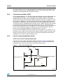
1
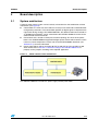
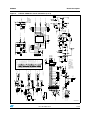
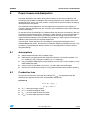
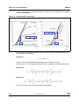
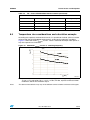
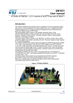
UM0969 User manual 3-phase motor control demonstration board featuring IGBT intelligent power module STGIPS10K60A Introduction This document describes the 1 kW 3-phase motor control demonstration board, featuring the STGIPS10K60A: 600 V - 10 A IGBT Intelligent power module. The demonstration board is a 3-phase inverter for driving an induction motor or PMSM motors up to 1000 W. The main target of this application is to show users the performance of the ST 25L-SDIP (25-lead, small dual inline package), IPM - STGIPS10K60A. The board has been designed to be compatible with a single-phase supply from 90 VAC to 220 VAC, or for DC voltage from 125 VDC to 350 VDC. The document is associated with the release of the STEVAL-IHM027V1 demonstration board (see Figure 1). Figure 1. STEVAL-IHM027V1 demonstration board February 2012 Doc ID 17665 Rev 2 1/46 www.st.com Contents UM0969 Contents 1 2 3 System introduction . . . . . . . . . . . . . . . . . . . . . . . . . . . . . . . . . . . . . . . . . 6 1.1 Main characteristics . . . . . . . . . . . . . . . . . . . . . . . . . . . . . . . . . . . . . . . . . . 6 1.2 Target application . . . . . . . . . . . . . . . . . . . . . . . . . . . . . . . . . . . . . . . . . . . . 6 1.3 Safety and operating instructions . . . . . . . . . . . . . . . . . . . . . . . . . . . . . . . . 7 1.3.1 General terms . . . . . . . . . . . . . . . . . . . . . . . . . . . . . . . . . . . . . . . . . . . . . 7 1.3.2 Demonstration board intended use . . . . . . . . . . . . . . . . . . . . . . . . . . . . . 7 1.3.3 Demonstration board installation . . . . . . . . . . . . . . . . . . . . . . . . . . . . . . . 7 1.3.4 Electrical connections . . . . . . . . . . . . . . . . . . . . . . . . . . . . . . . . . . . . . . . 8 Board description . . . . . . . . . . . . . . . . . . . . . . . . . . . . . . . . . . . . . . . . . . . 9 2.1 System architecture . . . . . . . . . . . . . . . . . . . . . . . . . . . . . . . . . . . . . . . . . . 9 2.2 Board schematics . . . . . . . . . . . . . . . . . . . . . . . . . . . . . . . . . . . . . . . . . . . 10 2.3 Circuit description . . . . . . . . . . . . . . . . . . . . . . . . . . . . . . . . . . . . . . . . . . . 12 2.3.1 Power supply . . . . . . . . . . . . . . . . . . . . . . . . . . . . . . . . . . . . . . . . . . . . . 12 2.3.2 Inrush limitation . . . . . . . . . . . . . . . . . . . . . . . . . . . . . . . . . . . . . . . . . . . 12 2.3.3 Brake function . . . . . . . . . . . . . . . . . . . . . . . . . . . . . . . . . . . . . . . . . . . . 12 2.3.4 Overcurrent protection (OCP) . . . . . . . . . . . . . . . . . . . . . . . . . . . . . . . . 13 2.3.5 Current sensing amplifying network . . . . . . . . . . . . . . . . . . . . . . . . . . . . 13 2.3.6 Tachometer and Hall/encoder input . . . . . . . . . . . . . . . . . . . . . . . . . . . . 16 2.3.7 Temperature feedback and overtemperature protection (OTP) . . . . . . . 16 Hardware setting of the STEVAL-IHM027V1 . . . . . . . . . . . . . . . . . . . . . 18 3.1 Hardware settings with single-shunt configuration . . . . . . . . . . . . . . . . . . 18 3.2 Hardware settings with three-shunt configuration . . . . . . . . . . . . . . . . . . 19 3.3 Hardware settings for input stage . . . . . . . . . . . . . . . . . . . . . . . . . . . . . . . 20 4 Description of jumpers, test pins, and connectors . . . . . . . . . . . . . . . 21 5 Connector placement . . . . . . . . . . . . . . . . . . . . . . . . . . . . . . . . . . . . . . . 26 6 BOM list . . . . . . . . . . . . . . . . . . . . . . . . . . . . . . . . . . . . . . . . . . . . . . . . . . 27 7 PCB layout . . . . . . . . . . . . . . . . . . . . . . . . . . . . . . . . . . . . . . . . . . . . . . . . 31 2/46 Doc ID 17665 Rev 2 UM0969 8 Contents Power losses and dissipation . . . . . . . . . . . . . . . . . . . . . . . . . . . . . . . . 35 8.1 Assumptions . . . . . . . . . . . . . . . . . . . . . . . . . . . . . . . . . . . . . . . . . . . . . . . 35 8.2 Conduction loss . . . . . . . . . . . . . . . . . . . . . . . . . . . . . . . . . . . . . . . . . . . . 35 8.3 Switching loss . . . . . . . . . . . . . . . . . . . . . . . . . . . . . . . . . . . . . . . . . . . . . . 37 8.4 Thermal impedance overview . . . . . . . . . . . . . . . . . . . . . . . . . . . . . . . . . 37 8.5 Temperature rise considerations and calculation example . . . . . . . . . . . . 39 9 Ordering information . . . . . . . . . . . . . . . . . . . . . . . . . . . . . . . . . . . . . . . 40 10 Using the STEVAL-IHM027V1 with STM32 FOC firmware library . . . . 41 11 Environmental considerations . . . . . . . . . . . . . . . . . . . . . . . . . . . . . . . . 42 12 Hardware requirements . . . . . . . . . . . . . . . . . . . . . . . . . . . . . . . . . . . . . 43 13 Software requirements . . . . . . . . . . . . . . . . . . . . . . . . . . . . . . . . . . . . . . 44 14 Conclusion . . . . . . . . . . . . . . . . . . . . . . . . . . . . . . . . . . . . . . . . . . . . . . . . 44 15 References . . . . . . . . . . . . . . . . . . . . . . . . . . . . . . . . . . . . . . . . . . . . . . . . 44 16 Revision history . . . . . . . . . . . . . . . . . . . . . . . . . . . . . . . . . . . . . . . . . . . 45 Doc ID 17665 Rev 2 3/46 List of tables UM0969 List of tables Table 1. Table 2. Table 3. Table 4. Table 5. Table 6. Table 7. Table 8. Table 9. Table 10. Table 11. 4/46 Jumper settings for a single-shunt or three-shunt configuration . . . . . . . . . . . . . . . . . . . . . 15 Internal IPM NTC details (see relevant section on the STGIPS10K60A datasheet). . . . . . 17 Jumper settings for single-shunt configuration . . . . . . . . . . . . . . . . . . . . . . . . . . . . . . . . . . 18 Jumper settings for three-shunt configuration . . . . . . . . . . . . . . . . . . . . . . . . . . . . . . . . . . 19 Input stage configuration details . . . . . . . . . . . . . . . . . . . . . . . . . . . . . . . . . . . . . . . . . . . . . 20 Jumpers description . . . . . . . . . . . . . . . . . . . . . . . . . . . . . . . . . . . . . . . . . . . . . . . . . . . . . . 21 Connector pinout description . . . . . . . . . . . . . . . . . . . . . . . . . . . . . . . . . . . . . . . . . . . . . . . 22 Testing points description . . . . . . . . . . . . . . . . . . . . . . . . . . . . . . . . . . . . . . . . . . . . . . . . . . 25 BOM list . . . . . . . . . . . . . . . . . . . . . . . . . . . . . . . . . . . . . . . . . . . . . . . . . . . . . . . . . . . . . . . 27 RC - Cauer STGIPS10K60A thermal network . . . . . . . . . . . . . . . . . . . . . . . . . . . . . . . . . . 38 Document revision history . . . . . . . . . . . . . . . . . . . . . . . . . . . . . . . . . . . . . . . . . . . . . . . . . 45 Doc ID 17665 Rev 2 UM0969 List of figures List of figures Figure 1. Figure 2. Figure 3. Figure 4. Figure 5. Figure 6. Figure 7. Figure 8. Figure 9. Figure 10. Figure 11. Figure 12. Figure 13. Figure 14. Figure 15. Figure 16. Figure 17. STEVAL-IHM027V1 demonstration board . . . . . . . . . . . . . . . . . . . . . . . . . . . . . . . . . . . . . . 1 Motor control system architecture. . . . . . . . . . . . . . . . . . . . . . . . . . . . . . . . . . . . . . . . . . . . . 9 STEVAL-IHM027V1 circuit schematics (1 of 1) . . . . . . . . . . . . . . . . . . . . . . . . . . . . . . . . . 10 STEVAL-IHM027V1 circuit schematics (2 of 2) . . . . . . . . . . . . . . . . . . . . . . . . . . . . . . . . . 11 STEVAL-IHM027V1 power supply block diagram . . . . . . . . . . . . . . . . . . . . . . . . . . . . . . . 12 Three-shunt configuration . . . . . . . . . . . . . . . . . . . . . . . . . . . . . . . . . . . . . . . . . . . . . . . . . . 13 Single-shunt configuration . . . . . . . . . . . . . . . . . . . . . . . . . . . . . . . . . . . . . . . . . . . . . . . . . 15 OT protection circuit . . . . . . . . . . . . . . . . . . . . . . . . . . . . . . . . . . . . . . . . . . . . . . . . . . . . . . 17 STEVAL-IHM027V1 input stage detail . . . . . . . . . . . . . . . . . . . . . . . . . . . . . . . . . . . . . . . . 20 Connector placement . . . . . . . . . . . . . . . . . . . . . . . . . . . . . . . . . . . . . . . . . . . . . . . . . . . . . 26 Copper tracks - top side . . . . . . . . . . . . . . . . . . . . . . . . . . . . . . . . . . . . . . . . . . . . . . . . . . . 31 Copper tracks - bottom side . . . . . . . . . . . . . . . . . . . . . . . . . . . . . . . . . . . . . . . . . . . . . . . . 32 Silk screen - top side . . . . . . . . . . . . . . . . . . . . . . . . . . . . . . . . . . . . . . . . . . . . . . . . . . . . . 33 Silk screen - bottom side . . . . . . . . . . . . . . . . . . . . . . . . . . . . . . . . . . . . . . . . . . . . . . . . . . 34 Static parameter calculations . . . . . . . . . . . . . . . . . . . . . . . . . . . . . . . . . . . . . . . . . . . . . . . 36 Equivalent STGIPS10K60A thermal network (CAUER models) . . . . . . . . . . . . . . . . . . . . . 38 Maximum IC(RMS) current vs. switching frequency . . . . . . . . . . . . . . . . . . . . . . . . . . . . . . 39 Doc ID 17665 Rev 2 5/46 System introduction UM0969 1 System introduction 1.1 Main characteristics The main characteristics of the STEVAL-IHM027V1 demonstration board are: 1.2 6/46 ● ST IGBT intelligent power module: STGIPS10K60A ● Minimum input voltage 125 VDC or 90 VAC ● Maximum input voltage 350 VDC or 220 VAC ● Possibility to use external +15 V supply voltage ● Maximum output power for motor up to 1000 W ● Regenerative brake control feature ● Input inrush limitation with bypassing relay ● +15 V auxiliary power supply based on buck converter with VIPer16 ● Fully populated board conception with testing points ● Motor control connector for interface with STM3210B-EVAL board and further ST motor control dedicated kits ● Tachometer input ● Hall\encoder inputs ● Possibility to connect BEMF daughter board for sensorless six-step control of BLDC motors ● PCB type and size: – Material of PCB: FR-4 – Double side layout – Copper thickness: ~45 µm – Dimension of demonstration board: 147 mm*157 mm Target application ● Domestic appliances ● Medical applications, fitness applications ● High power industry pumps ● Medium power fans for HVAC ● Power tools Doc ID 17665 Rev 2 UM0969 System introduction 1.3 Safety and operating instructions 1.3.1 General terms Warning: During assembly, testing, and normal operation, the demonstration board poses several inherent hazards, including bare wires, moving or rotating parts and hot surfaces. There is a danger of serious personal injury if the kit or components are improperly used or incorrectly installed. The kit is not electrically isolated from the AC/DC input. The demonstration board is directly linked to the mains voltage. No insulation is ensured between accessible parts and high voltage. All measuring equipment must be isolated from the mains before powering the board. When using an oscilloscope with the demonstration board, it must be isolated from the AC line. This prevents shock from occurring as a result of touching any SINGLE point in the circuit, but does NOT prevent shock when touching two or more points in the circuit. Do not touch the demonstration board after disconnection from the voltage supply; several parts and power terminals, which contain energized capacitors, must be allowed to discharge. All operations involving transportation, installation and use, as well as maintenance, are to be carried out by skilled technical personnel (national accident prevention rules must be observed). For the purpose of these basic safety instructions, “skilled technical personnel” are considered as suitably qualified people who are familiar with the installation, use, and maintenance of power electronic systems. 1.3.2 Demonstration board intended use The STEVAL-IHM027V1 demonstration board is designed for demonstration purposes only and must not be used for any commercial purposes. The technical data, as well as information concerning power supply conditions, must be taken from the relevant documentation and strictly observed. 1.3.3 Demonstration board installation The installation of the demonstration board must be in accordance with the specifications and the targeted application. ● The boards contain electro-statically sensitive components that are prone to damage through improper use. Electrical components must not be mechanically damaged or destroyed ● Avoid any contacts with other electronic components ● During the motor drive converters must be protected against excessive strain. In particular, no components are to be bent or isolating distances altered during the course of transportation or handling Doc ID 17665 Rev 2 7/46 System introduction 1.3.4 UM0969 Electrical connections Applicable national accident prevention rules must be followed when working on the main power supply with a motor drive. The electrical installation must be completed in accordance with the appropriate requirements. A system architecture which supplies power to the demonstration board must be equipped with additional control and protective devices in accordance with the applicable safety requirements (e.g. compliance with technical equipment and accident prevention rules). 8/46 Doc ID 17665 Rev 2 UM0969 Board description 2 Board description 2.1 System architecture A generic motor control system can be basically schematized as the combination of three main blocks (see Figure 2): ● Control block: the main task of this block is to accept user commands and board\motor configuration parameters. The control block provides all digital signals to implement the right motor driving strategy. The STM3210B-EVAL, ST demonstration board, based on an STM32 microcontroller, can be connected to the STEVAL-IHM027V1 thanks to the onboard motor control connector ● Power block: this is based on three-phase inverter topology. The heart of the power block is the STGIPS10K60A integrated intelligent power module which contains all the necessary active components. Please refer to the STGIPS10K60A datasheet (see References 1) for more information ● Power supply block: able to work from 90 VAC to 220 VAC or from 125 VDC to 350 VDC. Please refer to Section 3: Hardware setting of the STEVAL-IHM027V1, to properly set the jumpers according to the required application Figure 2. Motor control system architecture The STEVAL-IHM027V1 includes the power supply and the power block. Doc ID 17665 Rev 2 9/46 6!# * Doc ID 17665 Rev 2 LINE BAR "%-&?$AUGHTER "OARD 07- 6REF 6 6DD?M 6 07-?#, 07-?#( 4 4 &6? # 07-?", 07-?"( &6? # 07-?!, 07-?!( &6? # #/. * &6? # &6? # &6? # 6 # * * 34')03+! ,). (). 4 4 6"// 4 7 /54 7 '.$ ,). (). 6"// 4 6 /54 6 ,). (). 6## 6"// 4 5 /54 5 5 42 +%! % 7 0 % 6 0 % 5 0 ) ,OW 0HASE # ) (IGH 0HASE # 0HASE # 0HASE " 0HASE ! 4O BE SOLDERED 0HASE # N&6 0HASE " # $ 344 (, 0HASE ! N&68 5 # 7 2 " * ) ,OW 0HASE " N&6? # &6 # ) (IGH 0HASE ! $ ":8# M( , # # NC N&6? 2 ) ,OW 0HASE ! # N&6? 2 "53 ! 0(!3% /54054 # N&6? # N&6 ) (IGH 0HASE " ! 7 " 6)0%2,. #/-0 6$$ ,)&" N&6 2 "53 * * * * * # ( 2 0HASE # 6 * # N&6? * K7 2 * * 6)0%2 /./&& , 2 0HASE " # N&68 $ "2)$'% 6 2 # 2 + 2 + + 2 "53 # * 2ELAY 5 ). 5 342 )# # '.$ 1 . $ 2 2 K 2 K 6O UT ,#0 &6 6IN 6 /54 /54 /54 /54 ,$$ 2%,!9! &6 # '2%%. ,%$ ,$ ":8# $ + 2 # 6 &6 2ELAY N&6? # (6 "US 6 2 NC * $ 344 (,! &6 # N&6 N&6? 2 K K )NRUSH CURR 6 0OW &6 # 6 STEVAL-IHM027V1 circuit schematics (1 of 1) 0HASE ! & ! 2ELAY 24 .4# 2ELAY * 2 # $RAIN $RAIN $RAIN $RAIN 3OURCE 3OURCE 3OURCE 3OURCE "53 2 6$# "53 & ! K7 K7 2 '.$ K7 2 10/46 Figure 3. Board schematics 2.2 * Board description UM0969 !-V 7 *5-0 7 "!2 "!2 "!2 $ $ $ 7 7 ! " 6 6 2 K K 2 2 K P&6? # -EASURE 0HASE # 7 07- 6REF -EASURE 0HASE ! -EASURE 0HASE " #URRENT 0HASE ! #URRENT 0HASE " #URRENT 0HASE # )NRUSH CURR 07-?"RAKE &AULT # P&6? K 2 7 2 K K 2 436 5# K 2 #/.4 * 2 K *5-0 K 2 K 2 436 2 K 2 K TEMP "!2 $ K 5" K 2 # P&6? K 2 N&6? 436 # # P&6? 5! 2 K 6 5 43),4 6 # K 2 40 40 40 40 40 40 40 40 40 40 40 40 40 40 40 40 40 40 40 40 40 &AULT 1 6 9 9 9 9 9 9 342 K $ "!2 NC "53 K 2 K 6 342 1 # N6? " $ K 2 K K 5 K 2 2 K 5 43),4 K N&6? # &6 # 7 *5-0 4 4 # 2 K 2 K # P&6? 7 7 7 ,$ 2%$ ,%$ 2 K 2 K NC 2 1 6 TEMP #HANGE 2 TO SET THE .4# TEMPERATURE THRESHOLD -EASURE 0HASE # K K 2 1 34'&.#($ 342 1 344 ( $ -EASURE 0HASE " "53 -EASURE 0HASE ! 6 P&6? # $ 1 P&6? # 6DD?M 2 K 1 342 1 342 6 "RAKE CONTROL P&6? 2 K (EATSINK 4EMPERATURE -EASURE 0HASE ! N&6? # -(# # N&6? 6 2 07-?"RAKE K ":8#6 # N&6? 2 K 7 4 342 K N&6? # (!,, 3%.3/2 %.#/$%2 7 K ! K 2 $ "!2 # N&6? 342 1 K 6 * 1 K 2 6DD?M '.$ 07-?!( 07-?!, 07-?"( 07-?", 07-?#( 07-?#, $ ":8#6 -(#-2 N&6? # 6 ' '.$ ' ! ! ! ! ! ! 5 (ALL 6 0OW 66 (ALL "RAKE CONTROL 6 (ALL 4!#(/ * 6DD?M (6 "US -EASURE 0HASE # -EASURE 0HASE " -EASURE 0HASE ! #URRENT 0HASE # #URRENT 0HASE " #URRENT 0HASE ! 07-?#( 07-?#, 07-?"( 07-?", 07-?!( 07-?!, 0HASE # 0HASE " 0HASE ! 4EST POINTS ." WITH 2K 2K 2K THE CONTROL BRAKE WILL OPERATE AT 6 AND 6 07-?( 07-?, 07-?( 07-?, 07-?( 07-?, #URRENT 0HASE # 6DD?M /54 /0AMP #URRENT 0HASE " 6DD?M /54 /0AMP #URRENT 0HASE ! 6DD?M /54 /0AMP ALL RESISTOR AT "!2 $ "!2 $ "!2 $ 2 K /54 /0AMP /54 /0AMP 2 2 2 K K 2 2 K /54 /0AMP /#0 PROTECTION /&& 6 0OW 6DD?M "!2 # P&6? 2 2 K # P&6? (6 "US " $ *5-0 6 436 ) ,OW 0HASE # 5$ 6 7 ! 2 7 ) (IGH 0HASE # 2 # P&6? ) ,OW 0HASE ! ) ,OW 0HASE " 2 K 2 K (EATSINK 4EMPERATURE K 6 ) (IGH 0HASE " 6 ) (IGH 0HASE ! 2 2 6## &6 2 # 2 6 2 Doc ID 17665 Rev 2 2 2 2 2 K 2 2 2 K 2 2 2 K 2 2 2 2 2 2 . 2 2 2 2 2 * 2 "RAKE Figure 4. K 2 UM0969 Board description STEVAL-IHM027V1 circuit schematics (2 of 2) 2 K + 2 !-V 11/46 Board description UM0969 2.3 Circuit description 2.3.1 Power supply Power supply of the STEVAL-IHM027V1 is realized as a multifunctional block which allows the inverter to be supplied up to +350 V. The auxiliary power supply, needed for the active components on the demonstration board, is implemented with a buck converter based on U10 VIPer16, which works with a fixed frequency of 60 kHz. The +15 VDC output voltage is fed into VCC (STGIPS10K60A, PIN 5), as well as into the linear regulator L7805ICP, which provides a +5 VDC for supplying operational amplifiers and further related parts. The presence of +15 VDC on the board is indicated with a green LED (D1). Please refer to the VIPer16 datasheet (see References 2) for further information. Figure 5 below describes the power supply block diagram. Figure 5. STEVAL-IHM027V1 power supply block diagram нϭϱs ĞdžƚĞƌŶĂůƉŽǁĞƌƐƵƉƉůLJ ĐŽŶŶĞĐƚŽƌ :ϮϬ :ƵŵƉĞƌ s/WϭϲKŶͬKĨĨ /EWhd :ϱ ϮϮϬsͬ ϯϱϬs ƌŝĚŐĞZĞĐƚŝĨŝ Ğƌͬ sŽůƚĂŐĞŽƵďůĞƌ h^DyϰϬϬs͊ ƵĐŬŽŶǀĞƌƚĞƌ s/WĞƌϭϲ>E >ŝŶĞĂƌZĞŐƵůĂƚŽƌ >ϳϴϬϱW нϱs !-V 2.3.2 Inrush limitation The input stage of the demonstration board is provided with an NTC resistor (RT1) to eliminate input inrush current peak during bulk capacitors charging. It is possible to achieve a higher inverter efficiency to bypass this resistor after the startup phase. The driving signal of the bypassing relay is provided directly from the MCU board through the J3 motor control connector (pin 21). 2.3.3 Brake function A hardware brake feature has been implemented on the STEVAL-IHM027V1. An external resistor can be connected to the board thanks to the J4 connector. It represents a dummy load connected directly to the bus, in order to eliminate any overvoltage condition generated by the motor operating as a generator. Voltage on the bus is sensed through a voltage divider net (resistors R80, R81, and R82), and it is compared to the voltage reference of U6. The brake dummy load is switched on when the bus voltage reaches 390 VDC and switched off when the voltage decreases to below 330 VDC. 12/46 Doc ID 17665 Rev 2 UM0969 Board description The brake function can be also activated by the microcontroller thanks to the motor control connector (connector J3, pin 23 PWM_BRAKE signal). The brake threshold levels can be modified by calculating R83, R85, and R86 new values. 2.3.4 Overcurrent protection (OCP) On the STEVAL-IHM027V1 a simple overcurrent HW protection has been implemented. The three TSV994 outputs (pin 1, 7, 8) are the inputs for a discrete OR logic (realized with diodes D6,D7,D8). OR logic output, the biggest op-amp output voltage, is compared to a fixed threshold voltage (set by the R52-R49 voltage divider). When this threshold is passed, transistor Q1 is switched on, setting the enable signals to 0 V (/G1/G2) of M74HC367 and interrupting the PWM signal path, from the MCU to the STGIPS10K60A logic input. When an OCP event occurs, the FAULT signal (connector J3, pin 1 FAULT signal) is also activated to communicate with the MCU. The current protection limit value is also defined by the current sensing amplifying network, described in the next paragraph, because its value must be chosen according to the maximum amplifiable current without distortions. With the chosen value, the STEVAL-IHM027V1 OC protection limit is set to 6 A. The OCP can be disabled by moving the jumper W16 from position “A” to position “B”. It is possible to reach a higher current value but the demonstration board does not protect itself during an overcurrent event. This test must be carried out by skilled technical personnel according to the common accident prevention rules. Current sensing amplifying network Three-shunt current reading configuration Three-shunt current reading configuration details are shown in Figure 6. The alternating signal on the shunt resistor, with positive and negative values, must be elaborated to be compatible with the positive input of the microcontroller A/D converter. Figure 6. Three-shunt configuration 6 6 2 2 3HUNT2ESISTOR2S 2 5! 436 /54/P!MP 2.3.5 R 2 !-V Doc ID 17665 Rev 2 13/46 Board description UM0969 Default values for the STEVAL-IHM027V1 are: ● r = 1 kΩ (R11, R25, R30) ● R = 5.4 kΩ (R12-13, R21-22, R31-32) ● R1 = 560 Ω (R4, R15, R27) ● R2 = 560 Ω (R7, R18, R28) ● R3 = 4.7 kΩ (R1, R16, R26) The op amp is used in follower mode and its gain can be set by resistor r and R: Equation 1 G= R+r r VOUT (op amp output voltage) can be calculated as a sum of two components: ● VBIAS: due to network polarization ● VSIGN: the signal component Equation 2 VOUT = VSIGN + VBIAS VOUT maximum value is 3.3 V according to the MCU maximum input rating. Equation 3 VBIAS = 5 ⎛ 1 1 1 ⎞ ⎟ ⋅ R3 ⎜⎜ + + R 1 R 2 R 3⋅ ⎟⎠ ⋅ ⎝ ⋅ ⋅G Equation 4 VSIGN = I ⋅ Rs ⎛ 1 1 1 ⎞ ⎟ ⋅ R1 ⎜⎜ + + R 1 R 2 R 3 ⋅ ⎟⎠ ⋅ ⎝ ⋅ ⋅G Equation 5 GTOT = VSIGN G = Rs ⋅ I ⎛ 1 1 1 ⎞ ⎜⎜ ⎟ ⋅ R1 + + R 1 R 2 R 3⋅ ⎟⎠ ⋅ ⎝ ⋅ With the default values: ● G = 6.4 ● VBIAS = 1.8 V ● GTOT = 3 ● Maximum current amplifiable without distortion is 5 A It is possible to modify the maximum current value by simply changing the resistor values. 14/46 Doc ID 17665 Rev 2 UM0969 Board description Six-step (block commutation) current reading configuration In the case of six-step (also called block commutation) current control, only two motor phases conduct current at the same time. Therefore, it is possible to use only one shunt resistor. Moreover, as the current flows always in the same direction, only a positive value has to be measured. A proper amplifying network needs to be redesigned (see Figure 7). Figure 7. Single-shunt configuration 6 6 2 2 2 /54/P!MP 3HUNT2ESISTOR2S 5! 436 2 R 2 !-V See Table 1 to properly set the jumpers for single-shunt current reading: Table 1. Jumper settings for a single-shunt or three-shunt configuration Gain setting Jumper Single-shunt Three-shunt W2 Not present Present W4 B position A position W6 Not present Present W12 B position A position W13 B position A position Default values for the STEVAL-IHM027V1 are: ● r = 1 kΩ (R25) ● R = 5.4 kΩ + 5.6 kΩ (R21, R22, R23) ● ● ● ● R1 = 560 Ω + 470 Ω (R14, R15) R2 = 1000 kΩ (R20) R3 = 22 Ω (R24) R4 = 2.2 kΩ (R17) Doc ID 17665 Rev 2 15/46 Board description UM0969 The op amp is used in follower mode and its gain can be set by resistor r and R: Equation 6 G= R+r r VOUT (op amp output voltage) can be calculated as a sum of two components: ● VBIAS: due to network polarization ● VSIGN: the signal component Equation 7 VOUT = VSIGN + VBIAS VOUT maximum value is 3.3 V according to the MCU input maximum rating. Equation 8 VBIAS = [R1/(R1 + R2)]5 ⋅G ⎛ 1 ⎞ 1 1 ⎜⎜ ⎟⎟ ⋅ R4 + + ⎝ R4⋅ R3⋅ R1 + R2⋅ ⎠ Equation 9 VSIGN = ((R3 // R4) + R2)I ⋅ Rs ⋅G (R3 // R4) + R2 + R1 With the default values: ● G = 12 ● VBIAS = 0.3 V ● Maximum current amplifiable without distortion is 5 A It is possible to modify the maximum current value by simply changing the resistor values. 2.3.6 Tachometer and Hall/encoder input Both the tachometer and Hall/encoder inputs have been implemented on the STEVALIHM027V1. In the case of using a Hall or encoder sensor, the W1, W3, and W7 jumpers must be connected and the W8 jumper disconnected. The W5 jumper set in position A allows any connected Hall sensor to be supplied with the same supply voltage of the MCU (+3.3 VDC or +5 VDC depend on the W1 jumper). Setting the W12 jumper to position B supplies the Hall sensor directly with +5 VDC, which is the most common voltage for a Hall sensor. In the case of using a tachometer, the W1, W3, and W7 jumpers must be disconnected and the W8 jumper connected. This type of adjustable feature allows for the testing and evaluating of motors with a wide spectrum of various sensors. 2.3.7 Temperature feedback and overtemperature protection (OTP) The STGIPS10K60A integrates an NTC for temperature monitoring purposes. A simple voltage divider is realized with the internal NTC (see Table 2 for NTC details) and resistor R56. The temperature monitoring signal is sent to the MCU through J3 connector (pin 26 HEATSINK TEMPERATURE) and can be read with an AD converter. 16/46 Doc ID 17665 Rev 2 UM0969 Board description The STEVAL-IHM027V1 includes a hardware OT protection that stops the PWM signal path from the MCU to STGIPS10K60A logic input once the maximum allowable temperature is passed. With the chosen value, the OT protection limit is set to 70 °C. Another suggested scheme, generally adopted for temperature monitoring and protection, is shown in Figure 8. The NTC voltage is directly monitored by the MCU and an additional comparator enables/disables the board, according to the temperature thresholds. Figure 8. OT protection circuit Table 2. Internal IPM NTC details (see relevant section on the STGIPS10K60A datasheet) Symbol Parameter Test conditions R25 Resistance TC = 25 °C 5 kΩ R125 Resistance TC = 125 °C 300 Ω B B-constant TC = 25 °C 3435 K T Operating temperature P Max. rating power (max power on free air) Doc ID 17665 Rev 2 Min. Typ. -40 Max. 125 400 Unit °C mW 17/46 Hardware setting of the STEVAL-IHM027V1 3 UM0969 Hardware setting of the STEVAL-IHM027V1 The STEVAL-IHM027V1 demonstration board can be driven through the J3 motor connector by various control units released by STMicroelectronics. The demonstration board is suitable for field oriented control as well as for tachometer or Hall sensor closed-loop control. The STEVAL-IHM027V1 demonstration board ideally fits with the STMicroelectronics' released STM3210B-EVAL board, based on the STM32 MCU family, as the control unit for FOC driving algorithms. 3.1 Hardware settings with single-shunt configuration To drive any high PMSM or AC induction motor, the user must ensure that: ● The motor control demonstration board is driven by a control board that provides six output signals required to drive the 3-phase power stage ● The motor is connected to J2 motor output connector ● If using an encoder or Hall sensor, connect it to J1 ● If using a tachometer sensor, connect it to J24 ● If using the brake control feature, connect a dummy load to J4 Table 3 shows jumper settings for any motors. Please be sure that the input voltage (mains voltage) of the demonstration board is: from 90 VAC to 220 VAC or from 125 VDC to 350 VDC. Table 3. Jumper settings for single-shunt configuration Settings for single-shunt configuration Jumper 18/46 HV PMSM motor Generic AC motor with tachometer W1 Present Not present W2 Not present Not present W3 Present Not present W4 B position for single-shunt B position for single-shunt W5 B position to supply Hall sensor\encoder with +5 VCD B position to supply Hall sensor\encoder with +5 VCD W6 Not present Not present W7 Present Not present W8 Not present Present W9 User defined User defined W10 User defined User defined W11 User defined User defined W12 B position for single-shunt B position for single-shunt W13 B position for single-shunt B position for single-shunt W14 User defined User defined Doc ID 17665 Rev 2 UM0969 Hardware setting of the STEVAL-IHM027V1 Table 3. Jumper settings for single-shunt configuration (continued) Settings for single-shunt configuration Jumper 3.2 HV PMSM motor Generic AC motor with tachometer W15 User defined User defined W16 User defined User defined Hardware settings with three-shunt configuration To drive any high PMSM or AC induction motor, the user must ensure that: ● The motor control demonstration board is driven by a control board that provides six output signals required to drive the 3-phase power stage ● The motor is connected to J2 motor output connector ● If using an encoder or Hall sensor, connect it to J1 ● If using a tachometer sensor, connect it to J24 ● If using the brake control feature, connect a dummy load to J4 Table 4 shows jumper settings for any motors. Please be sure that input voltage (mains voltage) of the demonstration board is: from 90 VAC to 220 VAC or from 125 VDC to 350 VDC. Table 4. Jumper settings for three-shunt configuration Settings for three-shunt configuration Jumper HV PMSM motor Generic AC motor with tachometer W1 Present Not present W2 Present Present W3 Present Not present W4 A position for three-shunt A position for three-shunt W5 B position to supply Hall sensor\encoder with +5 VCD B position to supply Hall sensor\encoder with +5 VCD W6 Present Present W7 Present Not present W8 Not present Present W9 User defined User defined W10 User defined User defined W11 User defined User defined W12 A position for three-shunt A position for three-shunt W13 A position for three-shunt A position for three-shunt W14 User defined User defined W15 User defined User defined W16 User defined User defined Doc ID 17665 Rev 2 19/46 Hardware setting of the STEVAL-IHM027V1 3.3 UM0969 Hardware settings for input stage The input stage of the STEVAL-IHM027V1 can be configured according to user needs (see Figure 9). Please refer to Table 5 for detailed information. Figure 9. STEVAL-IHM027V1 input stage detail #64 3 ' " L8 #64 $ 7%$#64 7 + + %VQMJDBUPSF7BD 3 L8 3 % #3*%(& L8 + 53 ,&" $ 7 3FMBZ 3 3 8 L8 $ 3FMBZ O'79 ' + " 7"$ !-V Table 5. Input stage configuration details Description Connections Note Voltage doubler Connect J10 and J11 Maximum allowed DC voltage is 400 VDC Input capacitors series connections Connect J25-J13 and J12-J15 Input capacitors parallel connections Used to increase the input capacitance. Connect J23-J26 and J18-J14 Need to change the input capacitors if an increased voltage is required.(1) 1. If used with default capacitors never exceed the maximum voltage of 200 V 20/46 Doc ID 17665 Rev 2 Default connections (max DC voltage 400 V) UM0969 4 Description of jumpers, test pins, and connectors Description of jumpers, test pins, and connectors The following tables give a detailed description of the jumpers, test pins, and the pinout of the connectors used. Table 6 gives a detailed description of the jumpers. Table 7 gives a detailed description of the connectors while Table 8 describes all the test pins placed on the board. Table 6. Jumper Jumpers description Selection Description Present Connects tachometer signal to measure phase A Not present Disconnects tachometer signal to measure phase A Present Sets the gain of phase B current op. amplifier for three-shunt configuration Not present Sets the gain of phase B current op. amplifier for single-shunt configuration Present Connects tachometer signal to measure phase B Not present Disconnects tachometer signal to measure phase B A position Sets the gain of phase B current op. amplifier for three-shunt configuration B position Sets the gain of phase B current op. amplifier for single-shunt configuration A position Supply hall sensor\encoder with Vdd_m B position Supply hall sensor\encoder with +5 VDC Present Sets the gain of phase B current op. amplifier for three-shunt configuration Not present Sets the gain of phase B current op. amplifier for single-shunt configuration Present Connects tachometer signal to measure phase C Not present Disconnects tachometer signal to measure phase C Present Enable tachometer signal Not present Disable tachometer signal Present Set Vdd_m to +5 VDC Not present Set Vdd_m as the same voltage of MCU Present Supplies direct driving board through the J3 connector (max. current 50 mA) Not present Separated voltage Present Set Vdd_m to +3.3 VDC Not present Set Vdd_m as the same voltage of MCU A position Applies shunt resistor to C phase emitter leg B position Setting for single-shunt configuration A position Applies shunt resistor to A phase emitter leg B position Setting for single-shunt configuration Present “OTP” protection enabled Not present “OTP” protection disabled W1 W2 W3 W4 W5 W6 W7 W8 W9 W10 W11 W12 W13 W14 Doc ID 17665 Rev 2 21/46 Description of jumpers, test pins, and connectors Table 6. Jumper UM0969 Jumpers description (continued) Selection Description Present GIPS10K60A NTC signal enabled Not present GIPS10K60A NTC signal disabled A position “OCP” and “OTP” protection enabled B position “OCP” and “OTP” protection disabled W15 W16 Table 7. Name 22/46 Connector pinout description Reference DEscription\pinout J1 Hall sensor/encoder input connector 1 - Hall sensor input 1/encoder A+ 2 - Hall sensor input 2/encoder B+ 3 - Hall sensor input 3/encoder Z+ 4 - 5 VDC 5 - GND J2 Motor connector A - phase A B - phase B C - phase C Doc ID 17665 Rev 2 UM0969 Description of jumpers, test pins, and connectors Table 7. Name Connector pinout description (continued) Reference DEscription\pinout J3 Motor control connector 1 - emergency stop 2 - GND 3 - PWM - 1H 4 - GND 5 - PWM-1L 6 - GND 7 - PWM-2H 8 - GND 9 - PWM-2L 10 - GND 11 - PWM-3H 12 - GND 13 - PWM-3L 14 - HV bus voltage 15 - current phase A 16 - GND 17 - current phase B 18 - GND 19 - current phase C 20 - GND 21 - NTC bypass relay 22 - GND 23 - dissipative brake PWM 24 - GND 25 - +V power 26 - heatsink temperature 27 - PFC sync. 28 - VDD_m 29 - PWM VREF 30 - GND 31 - measure phase A 32 - GND 33 - measure phase B 34 - measure phase C J4 Dissipative brake 1 – open collector 2 – bus voltage Doc ID 17665 Rev 2 23/46 Description of jumpers, test pins, and connectors Table 7. Name 24/46 UM0969 Connector pinout description (continued) Reference DEscription\pinout J19 BEMF daughter board connector 1 - phase A 2 - phase B 3 - phase C 4 - bus voltage 5 - 3.3 VDC 6 - VDD_micro 7 - GND 8 - PWM VREF J20 +15 V auxiliary supply 1 – +15 VDC 2 – GND J21 DC input 1 – GND 2 – +VDC J22 AC input 1 – AC input 2 – AC input J24 Tachometer input connector for AC motor speed loop control 1 - tachometer bias 2 - tachometer input Doc ID 17665 Rev 2 UM0969 Description of jumpers, test pins, and connectors Table 8. Testing points description Test point Description TP1 Phase A TP2 Phase B TP3 Phase C TP4 PWM – phase A – low side TP5 PWM – phase A – high side TP6 PWM – phase B – low side TP7 PWM – phase B – high side TP8 PWM – phase C – low side TP9 PWM – phase C – high side TP10 Current phase A TP11 Current phase B TP12 Current phase C TP13 Encoder phase A TP14 Encoder phase B TP15 Encoder phase C TP16 HV bus TP17 Brake control TP18 +3.3 V TP19 +5 V TP20 +15 V TP21 GND Doc ID 17665 Rev 2 25/46 Connector placement 5 UM0969 Connector placement A basic description of the placement of all connectors on the board is visible in Figure 10. Figure 10. Connector placement 26/46 Doc ID 17665 Rev 2 BOM list A list of components used to build the demonstration board is shown in Table 9. The majority of the active components used are available from STMicroelectronics. Table 9. BOM list 27/46 6 BOM list Doc ID 17665 Rev 2 Value/part number Package Manufacturer C1, C54 4.7 µF/10 V Elyt. RM05mm KEMET C2,C5,C7,C14,C15,C16,C18,C37, C47,C55 100 nF/50 V SMD 1206 KEMET C3,C6,C12 33 pF/10 V SMD 1206 KEMET C4,C8,C9,C10,C11,C13 10 pF/10 V SMD 1206 KEMET C17 2.2 nF/10 V SMD 1206 KEMET C19 470 pF/10 V SMD 1206 KEMET C20,C27 1000 µ/200 V Elyt. RM30mm KEMET C21, C24,C29 100 µF-25 V Elyt. RM 150mils KEMET C22 2.2 µF/25 V Elyt. RM05mm KEMET C23, C28 220 nF/275 VAC X2 Polyester CK18 KEMET C25,C30 1 µF/16 V SMD 1206 KEMET C26 47 nF/16 V SMD 1206 KEMET C31,C32,C33 10 nF/400 V Polyester CK18 KEMET C34,C35,C38,C39,C43,C44 2.2 µF/50 V SMD 1206 KEMET C36 470 nF/25 V SMD 1206 KEMET C41,C42,C45 10 nF/10 V SMD 1206 KEMET C46 4.7 nF/10 V SMD 1206 KEMET C48 220 nF/50 V SMD 1206 KEMET C49 100 pF/10 V SMD 1206 KEMET UM0969 Reference BOM list (continued) Doc ID 17665 Rev 2 Value/part number Package Manufacturer D1,D2,D3,D4,D5,D6,D7,D8,D16,D19 BAR43 SOT23 STMicroelectronics D10 STTH1L06A SMD 1206 STMicroelectronics D18,D21 1N4148 DO35 Any D11 KBU6M Diode Bridge,250 VAC, 6 A Any D12 BZX84C18 MiniMelf Any D13 BZX85C16 MiniMelf Any D14 STTH1L06 DO-41 STMicroelectronics D15 STTH108 DO-41 STMicroelectronics D17,D20 BZX84C13V MiniMelf Any F1,F2 Fuse holder 5x20 mm Any Fuse 6A 20x5 mm Any IC2 L7805CP TO220FP STMicroelectronics LD1 Green LED Universal LED 3 mm, 2 mA Any LD2 Red LED Universal LED 3 mm, 2 mA Any L1 47 µH SMD CHOKE 0.5 A MAGNETICA L2 2.2 mH SMD CHOKE 0.25 A MAGNETICA T1,Q1,Q2,Q5,Q7,Q8,Q9,Q10,Q11 2STR1230 SOT-23 STMicroelectronics Q3,Q6 2STR2230 SOT-23 STMicroelectronics Q4 STGF7NC60HD TO220FP STMicroelectronics RT1 NTC 10 Ω EPCOS B57364S100M EPCOS R1,R2,R3,R5,R8,R9,R10,R16,R26 4.7 kΩ SMD 1206 Any R4,R7,R15,R18,R27,R28 560 Ω SMD 1206 Any R6,R11,R19,R20,R25,R29,R30,R87 1 kΩ SMD 1206 Any R12,R13,R21,R22,R31,R32 2.7 kΩ SMD 1206 Any R14 470 Ω SMD 1206 Any BOM list 28/46 Reference UM0969 Table 9. BOM list (continued) Doc ID 17665 Rev 2 Value/part number Package Manufacturer R17,R83 2.2 kΩ SMD 1206 Any R23,R99 5.6 kΩ SMD 1206 Any R24 22 Ω SMD 1206 Any R33,R35,R36,R44,R49,R76,R79R84 10 kΩ SMD 1206 Any R37,R54,R56,R69,R70,R71,R75R78 100 Ω SMD 1206 Any R38,R39,R40,R41,R42,R43,R92 47 kΩ SMD 1206 Any R45,R95 68 kΩ SMD 1206 Any R46,R88 100 kΩ SMD 1206 Any R48,R85 6.8 kΩ SMD 1206 Any R52 22 kΩ SMD 1206 Any R53,R57,R94 220 Ω SMD 1206 Any R55 680 Ω SMD 1206 Any R58,R77 1.8 kΩ SMD 1206 Any R59,R60,R64,R67 100 k-1/2 W RC06 Any R61,R63,R80,R81 470 kΩ SMD 1206 Any R62 1.5 kΩ SMD 1206 Any R65 8.2 kΩ SMD 1206 Any R72,R73,R74 0.1/5 W Low inductance sense resistor Any R82 27 kΩ SMD 1206 Any R86,R91 12 kΩ SMD 1206 Any R89 5.6 kΩ SMD 1206 Any R90 120 Ω SMD 1206 Any R96 220 kΩ SMD 1206 Any R98 15 kΩ SMD 1206 Any TR1 1.5KE400A DO-201 STMicroelectronics UM0969 Reference BOM list 29/46 Table 9. BOM list (continued) Reference Value/part number Package Manufacturer U1 TSV944 SO-14 STMicroelectronics U2 M74HC08 SO-14 STMicroelectronics U3 M74HC367M1R SO-16 STMicroelectronics U5 LD1117D33 SO-8 STMicroelectronics U6,U8 TS391ILT SOT23-5 STMicroelectronics U7 RELAY10A RELAY Finder U9 STGIPS10K60A SSDIP-25L STMicroelectronics U10 VIPER16LN SO-16 STMicroelectronics UM0969 Table 9. Doc ID 17665 Rev 2 BOM list 30/46 UM0969 7 PCB layout PCB layout For this application a standard, double-layer, coppered PCB with a ~45 µm copper thickness was selected. The PCB material is FR-4. The dimensions of the board are: ● Length: 147 mm ● Width: 157 mm ● PCB thickness:1.55 mm Figure 11. Copper tracks - top side Doc ID 17665 Rev 2 31/46 PCB layout UM0969 Figure 12. Copper tracks - bottom side 32/46 Doc ID 17665 Rev 2 UM0969 PCB layout Figure 13. Silk screen - top side Doc ID 17665 Rev 2 33/46 PCB layout UM0969 Figure 14. Silk screen - bottom side 34/46 Doc ID 17665 Rev 2 UM0969 8 Power losses and dissipation Power losses and dissipation The power dissipation of the IPM, during normal working, is due to the conduction and switching losses of IGBTs and diodes. The losses during the turn-off steady-state can be ignored, because of their very small amount, and because of the minor effect of increasing the temperature in the device. The conduction losses depend on the static electrical characteristics of the device (i.e. saturation voltage), therefore, they are a function of the conduction current and the device's junction temperature. On the other hand, the switching loss is determined by the dynamic characteristics, like turnon/off time and overvoltage/current. Therefore, in order to obtain an accurate estimation of the switching losses, it is necessary to consider the DC-link voltage of the system, the applied switching frequency, the sinusoidal carrier frequency, and the power circuit layout in addition to the load current and junction temperature. In this chapter, simple equations for calculating the average power dissipation of the STGIPS10K60A are shown. The power loss calculation intends to provide users with a way of selecting a matched power device, however, it is not expected to be used for thermal dissipation design. 8.1 Assumptions ● ● ● ● ● 8.2 PWM controlled inverter with sinusoidal output PWM signals are generated by the comparison between a sinusoidal waveform (at a fsine frequency) and a triangular waveform (at a fsw frequency) Duty amplitude of PWM signals varies between (1-ma)/2 and (1+ma)/2 where ma is the PWM modulation index Output current is sinusoidal (i=Ipeakcos(θ - φ)) and it does not include ripple Power factor of load output current is cos(φ); ideal inductive load is used for switching Conduction loss The typical characteristics of forward drop voltage (at Tjmax) are approximated by the following linear equation for the IGBT and the diode, respectively. Equation 10 vcesat = Vto _ I + Rce _ I ⋅ i vf = Vto _ D + Rd _ D ⋅ i ● ● ● ● Vto_I = threshold voltage of IGBT Vto_D = threshold voltage of diode Rce_I = on-state slope resistance of IGBT Rd_D = on-state slope resistance of diode Doc ID 17665 Rev 2 35/46 Power losses and dissipation UM0969 Figure 15 shows how to calculate the relevant parameters (values reported are not referred to the STGIPS10K60A). Figure 15. Static parameter calculations RD = ΔVF / ΔIF ΔIF RCE = ΔVCE / ΔIC ΔVF ΔIC ΔVCE VTO VFO AM07753v1 Assuming that the switching frequency is high, the output current of the PWM-inverter can be assumed to be sinusoidal. Equation 11 i = Ipeak cos(θ − φ) where φ is the phase-angle difference between output voltage and current. Using Equation 10, the conduction loss of one IGBT and diode can be obtained as follows: Equation 12 Equation 13 where ξ is the duty cycle in the given PWM control method: 36/46 Doc ID 17665 Rev 2 UM0969 Power losses and dissipation Equation 14 ε = [ 1 + ma cos(θ) ] / 2 and ma is the PWM modulation index (defined as the peak phase voltage divided by the half of dc link voltage). Finally, the integration of Equation 12 and Equation 13 gives: Equation 15 It should be noted that the total IPM conduction losses are six times the calculated Pcon. 8.3 Switching loss Switching losses can be divided into: turn-on power dissipation and turn-off power dissipation. The dynamic performances of the IGBT are strictly related to many parameters (voltage, current, temperature, etc.) so it is possible to make some assumptions to simplify the calculations. If the output current is sinusoidal, it is true if the switching frequency is high enough, also the switching power losses are sinusoidal: Equation 16 Eon(θ) = Eon _ peak cos(θ − φ) Eoff(θ) = Eoff _ peak cos(θ − φ) where Eon_peak and Eoff_peak are the maximum value @ Tjmax and Icpeak. Using Equation 16, the switching losses can be obtained as follows: Equation 17 8.4 Thermal impedance overview Semiconductor devices are very sensitive to junction temperature. This makes the thermal performances analysis of the IPM a very important factor during the application development stage. To start the analysis of the device's thermal behavior, the basic (and Doc ID 17665 Rev 2 37/46 Power losses and dissipation UM0969 fundamental) concept of thermal resistance must be considered, which is defined as the difference in temperature between two closed isothermal surfaces divided by the total power flow between them, Equation 18. Equation 18 For semiconductor devices, typically, the important factors are the relation between Tj, IGBT junction temperature, and a reference temperature, Tx. The selection of a reference point is arbitrary, but usually the hottest spot on the back of a device, on which a heatsink is attached, is chosen. This is called junction-to-case thermal resistance, Rφjc. When the reference point is an ambient temperature, it is called junction-to-ambient thermal resistance, Rφja. Both thermal resistances are used for the characterization of a device's thermal performance. The thermal resistance of the IPM is strictly related to the assembly process/material: STGIPS10K60A is based on a DBC substrate that guarantees a higher isolation voltage and an excellent thermal resistance value. In practical operations, the power loss PD is cyclic and therefore the transient RC equivalent thermal circuit, see Figure 16 and Table 10 for more details, should be considered. For pulsed power loss, the thermal capacitance effect delays the rise in junction temperature, and therefore permits a heavier loading of the IPM. Figure 16. Equivalent STGIPS10K60A thermal network (CAUER models) 4J 2 2 2 2 2 2 2 2 2 # # # # # # # # # 0TOT 4CASE !-V Table 10. RC - Cauer STGIPS10K60A thermal network RC - Cauer STGIPS10K60A thermal network 38/46 R Value [ºC/W] C Value [W*s/ºC] R1 0.088 C1 0.32E-3 R2 0.0154 C2 0.63E-3 R3 0.316 C3 0.90E-4 R4 0.395E-2 C4 0.50E-3 R5 0.816 C5 0.50E-2 Doc ID 17665 Rev 2 UM0969 Power losses and dissipation Table 10. RC - Cauer STGIPS10K60A thermal network (continued) RC - Cauer STGIPS10K60A thermal network 8.5 R Value [ºC/W] C Value [W*s/ºC] R6 0.432 C6 1.20E-2 R7 0.0123 C7 0.149E-2 R8 0.448 C8 0.809E-3 R9 1.66 C9 0.120 Temperature rise considerations and calculation example According to the previous mathematical formula, it is possible to simulate (with an accurate software tool) the STGIPS10K60A performances, under certain application conditions. Figure 17 shows the results (IC(RMS) current - which is related to the output motor power vs. fsw) of the power loss simulations. Figure 17. Maximum IC(RMS) current vs. switching frequency /Đ;ZD^Ϳ DĂdžŝŵƵŵ/Đ;ZD^ͿĐƵƌƌĞŶƚǀƐ͘ƐǁŝƚĐŚŝŶŐĨƌĞƋƵĞŶĐLJ ϭϬ dĐсϴϬΣ ϴ ϲ dĐсϭϬϬΣ ϰ Ϯ Ϭ Ϭ ϰ ϴ ϭϮ ϭϲ ϮϬ ĨƐǁŬ,nj ● Note: !-V Condition: VPN=300 V, VCC=VBS=15 V, VCE(sat)=typical, switching loss=typical, Tj=125 °C, Tc=see graph, Rth(j-c) = max., ma=0.8, PF=0.6, 3-phase continuous PWM modulation, 60 Hz sine waveform output. The above characteristics may vary in the different control schemes and motor drive types. Doc ID 17665 Rev 2 39/46 Ordering information 9 UM0969 Ordering information The demonstration board is available through the standard ordering system, the order code is: STEVAL-IHM027V1. The items delivered include the assembled board, board documentation, PCB fabrication data such as gerber files, assembly files (pick and place), and component documentation. 40/46 Doc ID 17665 Rev 2 UM0969 10 Using the STEVAL-IHM027V1 with STM32 FOC firmware library Using the STEVAL-IHM027V1 with STM32 FOC firmware library The STM32 FOC firmware library v2.0 is a firmware library running on the STM3210BMCKIT which allows the performing of the FOC of a PMSM (or ACIM) in a configuration with and without sensors. Doc ID 17665 Rev 2 41/46 Environmental considerations 11 UM0969 Environmental considerations Warning: The STEVAL-IHM027V1 demonstration board must only be used in a power laboratory. The voltage used in the drive system presents a shock hazard. The kit is not electrically isolated from the DC input. This topology is very common in motor drives. The microprocessor is grounded by the integrated ground of the DC bus. The microprocessor and associated circuitry are hot and MUST be isolated from user controls and communication interfaces. Warning: 42/46 All measuring equipment must be isolated from the main power supply before powering up the motor drive. To use an oscilloscope with the kit, it is safer to isolate the DC supply AND the oscilloscope. This prevents shock occurring as a result of touching any SINGLE point in the circuit, but does NOT prevent shock when touching two or more points in the circuit. Doc ID 17665 Rev 2 UM0969 12 Hardware requirements Hardware requirements To run the STEVAL-IHM027V1 together with the STM32 FOC firmware library, the following items are required: ● The board: STEVAL-IHM027V1 ● High voltage insulated AC power supply up to 230 VAC ● J-link programmer (not included in the package) ● J-link insulating board (not included in the package) ● 3-phase brushless motor with permanent magnet rotor or a generic 3-phase induction motor (not included in the package) ● Insulated oscilloscope (as needed) ● Insulated multimeter (as needed). Doc ID 17665 Rev 2 43/46 Software requirements 13 UM0969 Software requirements To customize, compile, and download the STM32 FOC firmware library v2.0 motor control firmware, the IAR tool “EWARM v5.30” must be installed. The free 32 kB limited version (referenced as “IAR Kickstand Kit™” version) is available for download at http://supp.iar.com/Download. 14 Conclusion This document describes the 1 kW 3-phase motor control STEVAL-IHM027V1 demonstration board based on IPM as a universal fully-evaluated platform. 15 References 1. 2. 3. 4. 5. 44/46 STGIPS10K60A datasheet VIPer16 datasheet STGF10NC60KD datasheet UM0379 UM0723 Doc ID 17665 Rev 2 UM0969 16 Revision history Revision history Table 11. Document revision history Date Revision Changes 08-Nov-2010 1 Initial release. 21-Feb-2012 2 Modified: schematics Doc ID 17665 Rev 2 45/46 UM0969 Please Read Carefully: Information in this document is provided solely in connection with ST products. STMicroelectronics NV and its subsidiaries (“ST”) reserve the right to make changes, corrections, modifications or improvements, to this document, and the products and services described herein at any time, without notice. All ST products are sold pursuant to ST’s terms and conditions of sale. Purchasers are solely responsible for the choice, selection and use of the ST products and services described herein, and ST assumes no liability whatsoever relating to the choice, selection or use of the ST products and services described herein. No license, express or implied, by estoppel or otherwise, to any intellectual property rights is granted under this document. If any part of this document refers to any third party products or services it shall not be deemed a license grant by ST for the use of such third party products or services, or any intellectual property contained therein or considered as a warranty covering the use in any manner whatsoever of such third party products or services or any intellectual property contained therein. UNLESS OTHERWISE SET FORTH IN ST’S TERMS AND CONDITIONS OF SALE ST DISCLAIMS ANY EXPRESS OR IMPLIED WARRANTY WITH RESPECT TO THE USE AND/OR SALE OF ST PRODUCTS INCLUDING WITHOUT LIMITATION IMPLIED WARRANTIES OF MERCHANTABILITY, FITNESS FOR A PARTICULAR PURPOSE (AND THEIR EQUIVALENTS UNDER THE LAWS OF ANY JURISDICTION), OR INFRINGEMENT OF ANY PATENT, COPYRIGHT OR OTHER INTELLECTUAL PROPERTY RIGHT. UNLESS EXPRESSLY APPROVED IN WRITING BY TWO AUTHORIZED ST REPRESENTATIVES, ST PRODUCTS ARE NOT RECOMMENDED, AUTHORIZED OR WARRANTED FOR USE IN MILITARY, AIR CRAFT, SPACE, LIFE SAVING, OR LIFE SUSTAINING APPLICATIONS, NOR IN PRODUCTS OR SYSTEMS WHERE FAILURE OR MALFUNCTION MAY RESULT IN PERSONAL INJURY, DEATH, OR SEVERE PROPERTY OR ENVIRONMENTAL DAMAGE. ST PRODUCTS WHICH ARE NOT SPECIFIED AS "AUTOMOTIVE GRADE" MAY ONLY BE USED IN AUTOMOTIVE APPLICATIONS AT USER’S OWN RISK. Resale of ST products with provisions different from the statements and/or technical features set forth in this document shall immediately void any warranty granted by ST for the ST product or service described herein and shall not create or extend in any manner whatsoever, any liability of ST. ST and the ST logo are trademarks or registered trademarks of ST in various countries. Information in this document supersedes and replaces all information previously supplied. The ST logo is a registered trademark of STMicroelectronics. All other names are the property of their respective owners. © 2012 STMicroelectronics - All rights reserved STMicroelectronics group of companies Australia - Belgium - Brazil - Canada - China - Czech Republic - Finland - France - Germany - Hong Kong - India - Israel - Italy - Japan Malaysia - Malta - Morocco - Philippines - Singapore - Spain - Sweden - Switzerland - United Kingdom - United States of America www.st.com 46/46 Doc ID 17665 Rev 2