1
Test and Measurement
Division
Service Manual
SIGNALGENERATOR
SML01
1090.3000.11
SML02
1090.3000.12
SML03
1090.3000.13
Volume 2
Service manual consists of 2 volumes
Printed in the Federal
Republic of Germany
1090.3123.24
22
E-3
SML
Tabbed Divider Overview
Tabbed Divider Overview
Safety Instructions
Certificate of Quality
Support Center Address
List of R&S Representatives
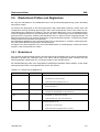
VOLUME 1
Basic Documents
Testing and Repair of Modules
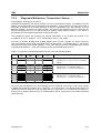
Mainboard............................................................................................................... Tabbed Divider 1
VOLUME 2
Testing and Repair of Modules
Front Assembly ...................................................................................................... Tabbed Divider 2
Attenuator ................................................................................................................. Tabbed Divider 3
Switching Power Supply ......................................................................................... Tabbed Divider 4
Reference Oscillator OXCO - Option SML-B1 ...................................................... Tabbed Divider 5
Pulse Modulator - Option SML-B3.......................................................................... Tabbed Divider 6
Output Unit ............................................................................................................... Tabbed Divider 7
1090.3123.24
RE
E-2
Serviceunterlagen
Frontmodul
1104.1409.12
ENGLISH SERVICE MANUAL FOLLOWS FIRST COLOURED DEVIDER
Printed in the Federal
Republic of Germany
1104.1409.00
1
D-1
SML
Frontmodul
Inhaltsverzeichnis
2 Frontmodul........................................................................................................... 2.1
2.1
Ausbau des Frontmoduls ..................................................................................................... 2.2
1104.1409.00
3
D-1
SML
2
Frontmodul
Frontmodul
Das Frontmodul enthält die Tastatur, den Drehgeber und das Display mit DC/AC-Wandler für die Beleuchtung. An der Frontplatte befinden sich außerdem der HF- bzw. RF-Ausgang und zwei BNCBuchsen (MOD, LF).
Tastatur, Drehgeber und Display werden direkt vom Mainboard aus angesteuert (Stecker X119, X118
und X117). Auch der DC/AC-Wandler für die Display-Beleuchtung wird von Mainboard aus versorgt
(Stecker X116). Hinweise für die Fehlersuche und die Schnittstellenbeschreibungen finden Sie in den
Serviceunterlagen zum Mainboard. Alle Komponenten enthalten keine Abgleichpunkte und müssen im
Fehlerfalle ausgewechselt werden.
1104.1409.00
2.1
D-1
Frontmodul
2.1
SML
Ausbau des Frontmoduls
Achtung!
Befolgen Sie bitte genau die Anweisungen der folgenden Abschnitte, damit eine Beschädigung des Geräts oder eine Gefährdung von Personen vermieden wird. Beachten
Sie bitte auch die allgemeinen Sicherheitshinweise am Anfang dieses Handbuchs.
Zum Ausbau des Frontmoduls verfahren Sie wie folgt:
Öffnen des Geräts
½
Das Gerät hochkant auf die beiden Griffe stellen, die vier Schrauben in den Gerätefüßen lösen.
Die Gerätefüße lassen sich nun entfernen.
½
Den Gehäusetubus vorsichtig nach oben abziehen.
Das Gerät ist jetzt offen.
Frontmodul ausbauen
½
Griffe seitlich an der Frontplatte abschrauben (je zwei Schrauben).
½
Frontblende abziehen.
½
Je drei Schrauben oben und unten im Frontrahmen lösen. Schraube links oben neben HF-Ausgang entfernen.
½
Alle Kabel vorsichtig abnehmen.
Das Frontmodul ist jetzt frei und kann herausgezogen werden.
Frontmodul einbauen
1104.1409.00
½
Schritte in umgekehrter Reihenfolge wie oben beschrieben ausführen.
2.2
D-1
Service Documents
Front Assembly
1104.1409.12
Printed in the Federal
Republic of Germany
1104.1409.00
1
E-1
SML
Front Assembly
Contents
2 Front Assembly.................................................................................................... 2.1
2.1
Removing the Front Assembly............................................................................................. 2.2
1104.1409.00
3
E-1
SML
2
Front Assembly
Front Assembly
The Front Assembly contains the keyboard, the spinwheel and the display with DC/AC converter for the
illumination. Besides, the front panel accommodates the RF output and four BNC connectors. Three of
these connectors are modulation inputs (EXT1, EXT2, PULSE). The forth connector is the input EXT
ALC for the external level control.
Keyboard, spinwheel and display are directly controlled from Mainboard A (connector X119, X118 and
X117). The DC/AC converter for the display illumination is also supplied from Mainboard A (connector
X116). Information on troubleshooting and the interface descriptions are to be found in the service
documents of Mainboard A. All the components do not include any trimming facilities and must be replaced in the case of an error.
1104.1409.00
2.1
E-1
Front Assembly
2.1
SML
Removing the Front Assembly
Caution!
Make sure to follow the instructions given in the following paragraphs in order not to
cause damage to the instrument or endanger anybody. Please also observe the general safety instructions at the beginning of this manual.
For removing the front module proceed as follows:
Opening the instrument
½
Put the instrument on end on both handles, ie loosen four screws
in the instrument feet.
The feet can now be removed.
½
Carefully lift off the instrument tube.
The instrument is now open.
Removing the front module
½
Unscrew the handles on the side of the front panel (two screws
each).
½
Pull off the front panel.
½
Loosen three screws both at the top and bottom of the front
frame. Remove the screw at the top left next to the RF output.
½
Carefully take off all cables.
The front module can now be pulled out.
Replacing the front module
1104.1409.00
½
Perform the steps in the reverse order to the procedure described
above.
2.2
E-1
Serviceunterlagen
Elektrische Eichleitung 1.1 GHz
1090.3700.02
ENGLISH SERVICE MANUAL FOLLOWS FIRST COLOURED DEVIDER
Printed in the Federal
Republic of Germany
1090.3700.00
1
D-2
SML
Elektrische Eichleitung 2.2 GHz
Inhaltsverzeichnis
3 Elektrische Eichleitung 2.2 GHz......................................................................... 3.1
3.1
Funktionsbeschreibung........................................................................................................ 3.1
3.1.1 Dämpfungsglieder ......................................................................................................... 3.1
3.1.2 Schalteransteuerung ..................................................................................................... 3.1
3.1.3 Überspannungsschutz................................................................................................... 3.1
3.1.4 Temperaturmessung ..................................................................................................... 3.2
3.1.5 Diagnose ....................................................................................................................... 3.2
3.1.6 Korrekturdatenspeicher ................................................................................................. 3.2
3.1.7 Ansteuerlogik................................................................................................................. 3.2
3.2
Ausbau der Elektrischen Eichleitung 2.2 GHz .................................................................... 3.3
3.3
Meßgeräte und Hilfsmittel..................................................................................................... 3.4
3.4
Messaufbau............................................................................................................................ 3.5
3.4.1 Grundkalibrierung.......................................................................................................... 3.5
3.5
Fehlersuche............................................................................................................................ 3.5
3.5.1 Lage der Testpunkte ..................................................................................................... 3.6
3.5.2 Selbsttest....................................................................................................................... 3.6
3.5.3 Ausgabe des Fehlerstatus............................................................................................. 3.6
3.5.4 Fehler 1: Eichleitung wird nicht erkannt ........................................................................ 3.7
3.5.5 Fehler 2: Frequenzgang außerhalb der Toleranz.......................................................... 3.7
3.5.6 Fehler 3: Ausgangspegel ist grob fehlerhaft.................................................................. 3.8
3.6
Prüfen und Abgleichen ....................................................................................................... 3.11
3.6.1 Prüfen der Dämpfungseinstellung ............................................................................... 3.11
3.6.2 Prüfen des Ausgangsreflexionsfaktors........................................................................ 3.11
3.6.3 Überspannungsschutz................................................................................................. 3.11
3.7
Externe Schnittstellen......................................................................................................... 3.12
1090.3700.00
3
D-1
Elektrische Eichleitung 2.2 GHz
SML
Index
A
Ansteuerlogik.....................................................................2
Ausbau ..........................................................................3, 4
D
Dämpfungseinstellung .....................................................10
Dämpfungsglieder ..............................................................1
Datenspeicher ...................................................................2
Diagnose ...........................................................................2
E
Externe Schnittstellen ......................................................12
F
Fehlersuchdiagramm .........................................................9
Fehlersuche.......................................................................5
Funktionsbeschreibung......................................................1
M
Meßaufbau ........................................................................5
Ö
Öffnen der Baugruppe .......................................................3
P
Prüfen..............................................................................11
S
Schalteransteuerung..........................................................1
T
Temperaturmessung..........................................................2
Ü
Überspannungsschutz .......................................................1
1090.3700.00
4
D-1
SML
3
Elektrische Eichleitung 2.2 GHz
Elektrische Eichleitung 2.2 GHz
Die Baugruppe Elektrische Eichleitung 2.2. GHz erlaubt im Frequenzbereich 9 kHz bis 2.2 GHz eine
Dämpfungsvariation im Bereich 0 bis 125 dB in 5 dB-Stufen.
3.1
Funktionsbeschreibung
Die Baugruppe Elektrische Eichleitung 2.2 GHz besteht aus den elektronisch umschaltbaren Dämpfungsgliedern, Schalteransteuerung, Überspannungsschutz, Temperaturmessung, Diagnoseteil, Korrekturdatenspeicher und Ansteuerlogik (siehe Stromlauf 1090.3700.02 S, Bl.-Nr. 1).
3.1.1
Dämpfungsglieder
Funktion
Dämpfungseinstellung 0 bis 125 dB in 5 dB-Stufen.
Eigenschaften
Die Abstufung der Dämpfungsglieder in 5, 10, 15, 30, 40 dB gestattet die Dämpfungseinstellung im Bereich 0 bis 125 dB mit 5 dB-Auflösung. Die Dämpfungsglieder sind in
5 Gruppen zusammengefaßt und mit GaAs-Schaltern geschaltet.
3.1.2
Schalteransteuerung
Funktion
Aufbereitung der Steuersignale für die GaAs-Dämpfungschalter.
Eigenschaften
Umwandlung der gespeicherten Einstelldaten mit logischem LV-Pegel in entsprechend verknüpfte symmetrische Steuerspannungen für GaAs-Schalter. Die Steuerspannungen sind abhängig vom eingestellten Dämpfungswert aufbereitet.
3.1.3
Überspannungsschutz
Funktion
Abschalten des HF-Ausgangs bei einer Überlastung der Eichleitung, falls externes
Signal unzulässiger Größe am Ausgang der Eichleitung eingespeist wird.
Eigenschaften
Nach einer Überschreitung des eingestellten Grenzwertes (Typ. 20 dBm) wird über
die Gleichrichterausgänge DET1 (2, 3) und Komparatoren U3, bzw. U4 das FlipFlop D1 aktiviert und der Störzustand gespeichert. Über die logische Verknüpfung
am D8 wird das Relais K1 ausgeschaltet und damit auch das Störsignal. Gleichzeitig wird Interrupt MI_OVRL an der Schnittstelle X301.17 ausgegeben. Während der
Reaktionszeit der Schutzschaltung wird das Störsignal durch V4+V5 auf einen zulässigen Wert begrenzt. Nach Beseitigung der Störungsursache muß D1 durch positiven Impuls an der Leitung OL_CLEAR wieder in den normalen Zustand versetzt
werden (bei SML bewirkt HF-ON den notwendigen Reset).
Beim Einschalten des Gerätes wird durch die Zeitkonstante R247+C161 der HFAusgang definiert ausgeschaltet. Das erste Einschalten des Relais K1 nach
‘Power_On‘ wird nicht zu den registrierten Überlastungsvorgängen gezählt.
1090.3700.00
3.1
D-1
Elektrische Eichleitung 2.2 GHz
3.1.4
SML
Temperaturmessung
Funktion
Die Temperaturmessung dient der Temperaturkorrektur der Dämpfungsdaten der
Eichleitung.
Eigenschaften
Die Differenz der aktuellen Temperaturspannung D_TEMP und der Ausgangsspannung D_MEM des D/A-Wandlers wird vom Fensterkomparator U2 überwacht. Der
gesetzte Interrupt MI_TEMP am X301.19 signalisiert Bedarf einer Aktualisierung der
Dämpfungsdaten durch veränderte Temperatur der Baugruppe. Durch die Korrektur
der Einstellung des D/A-Wandlers (U1+N6) wird die aktuelle Temperaturspannung
D_TEMP mit der Ausgangsspannung des D/A-Wandlers D_MEM kompensiert und
der Interrupt MI_TEMP gelöscht.
Bei reduzierten Anforderungen kann die Ausgabe des Interrupts über TMESS_ON
(=0) unterdrückt werden.
3.1.5
Diagnose
Funktion
Bestimmung der Spannungswerte an den signifikanten Diagnosestellen der Eichleitung.
Eigenschaften
Die Auswahl der Diagnosestellen und Ausgabe der Meßwerte an der Schnittstelle
X301.18 (V_DIAG) wird über den programmierbaren Analogmultiplexer D4 getroffen.
3.1.6
Korrekturdatenspeicher
Funktion
Identifikation der Baugruppe.
Eigenschaften
Der Datenspeicher enthält Daten zur Baugruppenidentifikation, Statistik- und Servicedaten sowie Korrekturdaten der Baugruppe und vereinfacht dadurch den Baugruppenaustausch.
Die Kommunikation mit dem Korrekturdatenspeicher D13 erfolgt über die serielle
Schnittstelle X301.14(EEDATA), X301.16(EECLK_N), selektiert über X301.11
(MS_ATTEN_N).
3.1.7
Ansteuerlogik
Funktion
Kommunikation mit der Gerätesteuerung über seriellen Datenbus.
Eigenschaften
Die Ansteuerlogik wandelt die seriellen Einstelldaten SERDATA_N (X301.13) parallel
um und speichert sie auf der Baugruppe. Im Register D10 sind Einstelldaten der
Dämpfungsschalter, im Register D11 sind Einstelldaten des DAC und im Register D12
sind Einstelldaten für Diagnose und Überspannungsschutz abgelegt. Die Kommunikation mit der Baugruppe erfolgt über die serielle Schnittstelle X301.13 (SERDATA_N),
X301.15 (SERCLK_N), X301.12(STROBE_N). Die Baugruppe wird über X301.11
(MS_ATTEN_N) selektiert. Nach der Übertragung eines 24 Bit-Datenwortes werden
die Daten mit STROBE_N in den Registerspeicher als gültige Einstellung übernommen (Bild 3-1).
1090.3700.00
3.2
D-1
SML
Elektrische Eichleitung 2.2 GHz
MS_ATTEN_N
SERCLK_N
SERDATA_N
STROBE_N
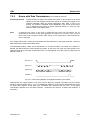
Bild 3-1
Eichleitungsprogrammierung, Zeitablauf an der Schnittstelle X301.
3.2
Ausbau der Elektrischen Eichleitung 2.2 GHz
Achtung!
Befolgen Sie bitte genau die Anweisungen der folgenden Abschnitte, damit eine Beschädigung des Geräts oder eine Gefährdung von Personen vermieden wird. Beachten
Sie bitte auch die allgemeinen Sicherheitshinweise am Anfang dieses Handbuchs.
Zum Öffnen der Eichleitung 2.2. GHz verfahren Sie wie folgt:
Öffnen des Gerätes
½
SML hochkant auf die beiden Griffe stellen und die vier Schrauben in den Gerätefüßen lösen.
Die Gerätefüße lassen sich nun entfernen.
½
Den Gehäusetubus vorsichtig nach oben abziehen.
Das Gerät ist jetzt offen.
Baugruppen ausbauen
½
Flachbandkabel W301 zur Baugruppe lösen.
½
Die Befestigungsschrauben zum Trägerblech lösen.
½
Beide SMA Schraubverbindungen W303, W106 lösen.
Die Baugruppe kann entnommen werden.
Baugruppe öffnen
Baugruppen einbauen
½
Die Befestigungsschrauben des Schirmdeckels lösen und den
Schirmdeckel abnehmen.
½
Bemerkung: Der Test der Schaltspannungen der GaAs-Schalter
kann beim abgenommenen oberen Schirmdeckel (Bestückungsseite) ohne Ausbau der Baugruppe vorgenommen werden.
½
Schritte in umgekehrter Reihenfolge wie oben beschrieben
durchführen.
Die SMA Schraubverbindung W303 am Ausgang der Baugruppe
muß vor dem Anziehen der Befestigungsschrauben zum Trägerblech angezogen werden.
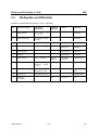
Die in der folgenden Tabelle aufgelisteten Geräte sind zum Prüfen der Baugruppe Elektrische
Eichleitung 2.2 GHz erforderlich.
1090.3700.00
3.3
D-1
Elektrische Eichleitung 2.2 GHz
3.3
SML
Meßgeräte und Hilfsmittel
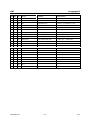
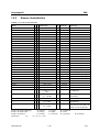
Tabelle 3-1 Elektrische Eichleitung 2.2. GHz – Hilfsmittel
Pos.
Geräteart, Hilfsmittel
Erforderliche
Eigenschaften
Geeignetes
R&S-Gerät
1
Digitalmultimeter
1 mV ... 100 V
0,1 mA ... 1 A
Fehlersuche
2
Speicheroszilloskop
DC-100 MHz, <0,1V/Div,
2 Kanäle
Fehlersuche
3
Servicekitt
4
Servicehandbuch SML (D)
SML-Z22
Bestell-Nr.
Anwendung
1090.5203.02
Fehlersuche
1090.3123.xx
Prüfen und
Abgleichen
5
Bestückungsplan
1090.3700.01 D
Fehlersuche
6
Stromlauf
1090.3700.01 S
Fehlersuche
7
Leistungsmesser
9 kHz ... ≥2200 MHz
NRVS mit
NRV-Z51
1020.1809.02
857.9004.02
Pegelgenauigkeit
8
Präzisionseichleitung
9 kHz ... ≥2200 MHz
Dämpfung 0 ... 125 dB
Z = 50 Ω
RSP
0831.3515.02
Pegelgenauigkeit
9
VSWR-Meßbrücke
1 MHz ... ≥2200 MHz
Richtschärfe > 40 dB
ZRC
1039.9492.55/52
Ausgangsreflexionsfaktor
10
Steuerrechner
Schnittstelle IEC-625-1
11
Steuergerät
für Eichleitung
1090.3700.00
Pegelgenauigkeit
SML
3.4
1090.3000.xx
Alle
D-1
SML
Elektrische Eichleitung 2.2 GHz
3.4
Meßaufbau
3.4.1
Grundkalibrierung
Meßmittel
Leistungsmesser
Steuerrechner
(Tabelle Meßgeräte und Hilfsmittel, Pos. 7)
(Tabelle Meßgeräte und Hilfsmittel, Pos. 10)
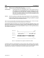
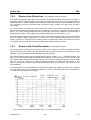
Meßaufbau
Rechner
IEC-Bus
RF
3.5
Leistungsmesser
Fehlersuche
Kurze Einleitung zur Fehlersuche auf der Elektrischen Eichleitung 2.2 GHz.
Die Fehler können auf der Basis des SML-Fehlerstatus-Reports und mit Hilfe des Servicekitts SML-Z22
im Grundgerät SML lokalisiert werden. Im Menüpunkt ‘Direct Mode ‘ können auch komplizierte Einstellungen an der Eichleitung vorgenommen werden. Bei der Fehlerdiagnose ist zu beachten, daß mehrere
Fehler eventuell eine gemeinsame Ursache haben können (z. B. kein Signal am HF-Ausgang).
Die DC-Spannungen an den im Schaltplan der Eichleitung, Blatt 4, angegebenen Diagnosepunkten
D_XXX (z. B. D_TEMP) können im Display des SML angezeigt werden. Für die Eichleitung (SML-Modul 6)
ist ein Diagnosetestbereich 600-605 reserviert. Hierzu wird im Untermenü Utilities/Diag/Tpoint die DiagnoseAnzeige aktiviert (State On) und der gewünschte Diagnosepunkt (siehe Tabelle 3-2) eingegeben.
Tabelle 3-2 Auswahl der Diagnosepunkte
Adresse
Diagnosepunkt
600
D_OFFSET
601
D_TEMP
602
D_DIFF
603
D_MEM
604
D_REF
605
D_RFOUT
Mit Hilfe des Servicekitts SML-Z22 kann die Baugruppe schnell getestet werden. Für den Funktionstest
ist im Hauptmenü die Option ‘Check / ATT2‘zu wählen. Die Testergebnisse werden im Testprotokoll
festgehalten und zusätzlich im Blockschaltbild graphisch dargestellt.
Im Menü ‘Direct Mode / Modules & Options / Att2 / Direct Mode ATT2‘ können auch gezielte Einstellungen (Tabelle 3-3) an der Eichleitung bei der Fehlersuche vorgenommen werden.
1090.3700.00
3.5
D-1
Elektrische Eichleitung 2.2 GHz
SML
Tabelle 3-3 Einstellungen im Menü ‘Direct Mode ATT2‘.
3.5.1
Menüpunkt
Wertebereich
Funktion
TEMP
0, 1,..., 255
DAC-Einstellung für die Temperaturkompensation
OFFS2_N
0/1
Offsetschalter für SW6 / SW6_N,
SW7_X / SW7_N_X
SWI
0, 1, ... (s. Tabelle 3-4)
Dämpfungseinstellung
TMESS_ON
0/1
Abschalten des Interrupts MI_TEMP
OFFS1_N
0/1
(s.Tabelle 3-4)
(s. Tabelle 3-4)
Offsetschalter für SW7 / SW7_N
Lage der Testpunkte
Die Diagnosetestpunkte befinden sich auf der unteren Seite (A-Seite im Bestückungsplan) der Eichleitung. Die genaue Position der Testpunkte (Bauelementanschluß) ist aus dem Bestückungsplan
1090.370.01 D ersichtlich.
Für die RF-Signalverfolgung und den Test der Steuerspannungen der GaAs-Schalter ist der Zugang zu
der Bestückungsseite (B-Seite im Bestückungsplan) nach Abnahme des oberen Schirmdeckels ausreichend.
3.5.2
Selbsttest
Nach dem Einschalten des SML werden Selbsttestmessungen durchgeführt. Ein fehlerhafter Selbsttestparameter führt zur Ausgabe einer Warnung ‘Err.....‘ im Display. Eine Kurzinformation über die Ursache
der Warnung, den Fehlerstatus, kann mit der Taste ‘ERROR‘ abgerufen werden. Weitere Informationen
über den Zustand der Baugruppe können im Menü Utilities/Diag/Tpoint abgerufen werden.
3.5.3
Ausgabe des Fehlerstatus
Der vollständige Fehlerstatus kann über die Fernbedienungsschnittstellen des SML (RS-232-C oder
IEC-Bus-Schnittstelle) abgefragt werden. Die Grundsätze der SML-Fernbedienung sind im Betriebshandbuch SML, Kapitel 5 zusammengefaßt.
Fehlerstatus-Abfrage:
1090.3700.00
"STAT:ERR?“
3.6
D-1
SML
3.5.4
Elektrische Eichleitung 2.2 GHz
Fehler 1: Eichleitung wird nicht erkannt
Fehlerbeschreibung
Fehlermeldung nach dem Einschalten des SML:
Module (6/ATT) Missing Data Block
6 / ATTENUATOR HEADER
10601 / FREQ DATA ATT
Meßaufbau
SML über externe Schnittstelle am PC angeschlossen.
Eichleitung aus dem SML ausgebaut und über W106 und Flachbandkabel W301 am SML angeschlossen.
Fehlerursache
Kommunikation mit Datenspeicher der Eichleitung ist gestört. Flachbandkabel W301 möglicherweise defekt oder die Daten /EEPROM
sind fehlerhaft.
½ In der Selbsttestphase nach dem Einschalten des SML, das Signal
an X301.15 und X301.16, während am X301.11 log. ‘L‘ angelegt
ist (Eichleitung selektiert, vgl. Bild 3-1), mit Speicheroszilloskop
prüfen. Signal eventuell bis D13 (Datenspeicher, Stromlaufblatt 2)
verfolgen.
Fehlerbehebung
3.5.5
½ Defektes Flachbandkabel ersetzen.
½ Fehlende Daten müssen neu aufgenommen werden (nur im Werk
oder in Servicestellen mit Spezialausrüstung möglich). Fehlerhafte
Baugruppe ersetzen.
½ Grundkalibrierung mit dem Servicekitt SML-Z22 (Menüpunkt
‘Calibrate-External-Level Correction‘) vornehmen.
Fehler 2: Frequenzgang außerhalb der Toleranz
Fehlerbeschreibung
½ Pegel prinzipiell in Ordnung, Frequenzgang zu groß.
Fehlerursache
½ Korrekturdatensatz fehlerhaft.
Fehlerbehebung
½ Pegelkorrekturwerte der Eichleitung müssen neu aufgenommen
werden (nur im Werk oder in Servicestellen mit Spezialausrüstung
möglich). Baugruppe ersetzen und die Grundkalibrierung mit dem
Servicekitt SML-Z22 (Menüpunkt ‘Calibrate-External-Level Corretion‘) vornehmen.
1090.3700.00
3.7
D-1
Elektrische Eichleitung 2.2 GHz
3.5.6
SML
Fehler 3: Ausgangspegel ist grob fehlerhaft
Fehlerbeschreibung
½ Kein Pegel am RF-Ausgang oder grobe Pegelfehler.
Messaufbau
½ Eichleitung am SML angeschlossen. Steuergerät (PC) am SML
angeschlossen.
½ Für die RF-Signalverfolgung und Test der Steuerspannungen der
GaAs-Schalter ist Ausbau des oberen Schirmdeckels ausreichend.
½ Leistungsmeßgerät an der RF-Ausgangsbuchse angeschlossen.
Fehlersuche
½ Mit Hilfe des Testprogramms im Servicekitt SML-Z22, Menüpunkt
CHECK/ATTENUATOR, die Eichleitung prüfen. Die Prüfergebnisse
geben Anhaltspunkte über die Funktion der GaAs-Schalter.
½ SML-Ausgangssignal 10 dBm, 100 MHz einstellen (Direct Mode).
½ Die Fehlersuche an Hand des Flußdiagramms in Bild 3-2 und des
Stromlaufs vornehmen. Die Schalterstellungen können im Menü
‘Direct Mode / Modules & Options / Att2‘ entsprechend Tabelle 3-4
eingestellt und die resultierenden Hardware-Reaktionen kontrolliert
werden. Der logische Wert 0 entspricht der Schalterstellung des
Dämpfungspfades mit der kleineren Dämpfung. Die Steuerspannungen (SWx/SWx_N) der GaAs-Schalter müssen im Bereich
SWx ≥0V (≤-4.5 V)/SWx_N ≤-4.5 V (≥0 V) liegen.
Fehlerbehebung
½ a)
1090.3700.00
Ein Fehler im Bereich der Schaltersteuerung (außerhalb der
dämpfungsmaßgebenden Pfade ohne Einfluß auf die HFEigenschaften) kann ohne Kalibrierung vor Ort behoben
werden.
½ b) Fehler im HF-Zweig. Fehlerhafte Baugruppe ersetzen. Nach
der Reparatur müssen Pegelkorrekturwerte neu aufgenommen werden (nur im Werk oder Servicestellen mit Spezialausrüstung möglich).
½ Grundkalibrierung mit dem Servicekitt SML-Z22 (Menüpunkt
‘Calibrate-External-Level Correction‘) vornehmen.
3.8
D-1
SML
Elektrische Eichleitung 2.2 GHz
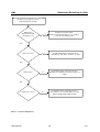
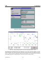
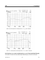
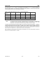
Am SML RF-Signal mit 100 MHz und 10 dBm
einstellen und das Signal mit einem
Oszilloskoptastkopf verfolgen.
Messwert am
Diagnosepunkt 0601
(D_RFOUT) > 0,1V
Ja
Überspannungsschutz prüfen.
Relais K1 und die Steuerlogik (V1..V7, V12/Bl. 8,
U3,U4, D1, D8, D9/Bl.4) prüfen.
Nein
Fehler an S1, S9 ?
Ja
RF-Signalpfad prüfen, Ansteuerung für S1
(SW1/SW1_N, SWI1/SWI1_N, Blatt 3, 2) prüfen
Fehler an S10 ?
Ja
RF-Signalpfad prüfen. Ansteuerung für S10
(SW6/SW6_N, SWI6/SWI6_N, OFFS2_N, Blatt 3, 2)
prüfen.
Fehler an S11, S13 ?
Ja
RF-Signalpfad prüfen, Ansteuerung für S11
(SW7_X/SW7_N_X ), bzw. SW7/SW7_N für S13
(Blatt 3) und SW7/SWI7 (Blatt 2) prüfen.
Nein
Nein
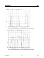
Bild 3-2 Fehlersuchdiagramm
1090.3700.00
3.9
D-1
Elektrische Eichleitung 2.2 GHz
SML
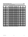
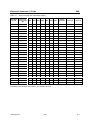
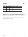
Tabelle 3-4 Servicekitt SML-Z22, Dämpfungseinstellung.
Dämpfungsstufe /dB
Ausgangspegelbereich @
X303 /dB
SWI1
SWI2
SWI3
SWI4
SWI5
SWI6
SWI7
Einstellwert
SWI
OFFS2_N
OFFS1_N
0
>5
0
0
0
0
0
0
0
00h
0
0
5
5 ... > 0
1
0
0
0
0
0
0
01h
0
0
10
0 ... >-5
1
1
0
0
0
0
0
03h
0
0
15
-5 ... >-10
1
1
1
0
0
0
0
07h
0
0
20
-10 ... >-15
1
0
0
1
0
0
0
09h
0
1
25
-15 ... >-20
1
1
0
1
0
0
0
0Bh
1
1
30
-20 ... >-25
1
1
1
1
0
0
0
0Fh
1
1
35
-25 ... >-30
1
0
0
1
1
0
0
19h
1
1
40
-30 ... >-35
1
1
0
1
1
0
0
1Bh
1
1
45
-35 ... >-40
1
0
0
0
0
0
1
41h
0
1
50
-40 ... >-45
1
1
0
0
0
0
1
43h
0
1
55
-45 ... >-50
1
1
1
0
0
0
1
47h
0
1
60
-50 ... >-55
1
0
0
1
0
0
1
49h
1
1
65
-55 ... >-60
1
1
0
1
0
0
1
4Bh
1
1
70
-60 ... >-65
1
1
1
1
0
0
1
4Fh
1
1
75
-65 ... >-70
1
0
0
1
1
0
1
59h
1
1
80
-70 ... >-75
1
1
0
1
1
0
1
5Bh
1
1
85
-75 ... >-80
1
0
0
0
0
1
1
61h
0
1
90
-80 ... >-85
1
1
0
0
0
1
1
63h
0
1
95
-85 ... >-90
1
1
1
0
0
1
1
67h
0
1
100
-90 ... >-95
1
0
0
1
0
1
1
69h
1
1
105
-95 ... >-100
1
1
0
1
0
1
1
6Bh
1
1
110
-100 ... >-105
1
1
1
1
0
1
1
6Fh
1
1
115
-105 ... >-110
1
0
0
1
1
1
1
79h
1
1
120
-110 ... >-115
1
1
0
1
1
1
1
7Bh
1
1
125
-115 ... >-120
1
1
1
1
1
1
1
7Fh
1
1
Die Einstellungen werden im D10, OFFS1_N wird im D12.12, gespeichert.
1090.3700.00
3.10
D-1
SML
3.6
Elektrische Eichleitung 2.2 GHz
Prüfen und Abgleichen
Die Baugruppe enthält keine Abgleichelemente, die Prüfung erfolgt zusammen mit dem SML nach BHB
Abschnitt 10, Performance Test – Pegel. Die Kalibrierung der Baugruppe ist nur im Werk oder in den
Servicestellen mit Spezialausrüstung möglich.
3.6.1
Prüfen der Dämpfungseinstellung
Die Prüfung wird mit einem SML nach der Grundkalibrierung mit der geprüften Eichleitung gemäß BHB
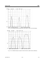
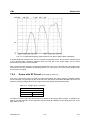
Abschnitt 10, Performance Test /Pegelfrequenzgang und /Pegellinearität, vorgenommen.
3.6.2
Prüfen des Ausgangsreflexionsfaktors
Die Prüfung wird mit einem SML nach der Grundkalibrierung mit der geprüften Eichleitung mit dem Servicekitt SML-Z22 gemäß BHB Abschnitt 10, Performance Test/Ausgangsreflexionsfaktor vorgenommen.
3.6.3
Überspannungsschutz
Die Prüfung wird mit einem SML gemäß Abschnitt 10, Performance Test/Überspannungsschutz vorgenommen.
1090.3700.00
3.11
D-1
Elektrische Eichleitung 2.2 GHz
3.7
SML
Externe Schnittstellen
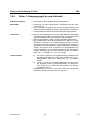
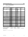
Tabelle 3-5 Externe Schnittstellen
Signal
Name
Beschreibung
R
A
GND
Masse
B
P
+12VM
Versorgungsspannung
I
P
-12VM
Versorgungsspannung
I
+5VM
Versorgungsspannung
+3VM
Versorgungsspannung
Wertebereich
PT
Anschlußpunkt
D
X301.1
X301.3
X301.5
X301.7
X301.9
11,6 V ... 12,4 V
P
X301.4
P
-12,4 V ... –11,6 V
P
X301.6
I
P
4,9 V ... 5,1 V
P
X301.8
I
P
2,9 V ... 3,1 V
P
X301.8
MS_ATTEN_N Baugruppe-Select
I
D
LVT
D
X301.11
STROBE_N
Speicher-Strobe
I
D
LVT
D
X301.12
SERDATA_N
Einstelldaten
I
D
LVT
D
X301.13
EEDATA
Identifikationsdaten
B
D
LVT
D
X301.14
SERCLK_N
CLK / Einstelldaten
I
D
LVT
D
X301.15
EECLK_N
CLK / Ident.-Daten
I
D
LVT
D
X301.16
MI_OVERL
Interrupt / Überspannungsschutz
O
D
LVT
P
X301.17
V_DIAG
Diagnosespannung
O
A
-1 ... 3 V
P
X301.18
MI_TEMP
Interrupt/Temperatur
O
D
LVT
P
X301.19
n.c.
X301.2
X301.20
RF IN
HF-Eingang
I
A
0 ... 20 dBm
P
X302
RF OUT
HF-Ausgang
O
A
0 ... 16 dBm
P
X303
Eintrag in der Spalte R (Richtung):
O = Ausgang
I = Eingang
Eintrag in der Spalte A (Art):
A = Analog
D = Digital
P = Power
Eintrag in der Spalte PT:
(Prüf- und Trimmplan)
P = Prüfwert
T = Trimmwert
D = Typprüfwert
Abkürzungen: LVT:
1090.3700.00
Bemerkung
PMAX ≤ 50 W
B = Bidirektional
E = Einstellwert
VOH ≥ 2V, VOL ≤ 0.55V
3.12
D-1
Service Documents
Electronic Attenuator 1.1 GHz
1090.3700.02
Printed in the Federal
Republic of Germany
1090.3700.00
1
E-2
SML
Electronic Attenuator 2.2 GHz
Contents
3 Electronic Attenuator 2.2 GHz ............................................................................ 3.1
3.1
Function Description............................................................................................................. 3.1
Attenuator Pads ....................................................................................................................... 3.1
3.1.1 Switch Control ............................................................................................................... 3.1
3.1.2 Over-voltage Protection................................................................................................. 3.1
3.1.3 Temperature Measurement........................................................................................... 3.2
3.1.4 Diagnosis....................................................................................................................... 3.2
3.1.5 Correction Data Memory ............................................................................................... 3.2
3.1.6 Control Logic ................................................................................................................. 3.2
3.2
Removing the Electronic Attenuator 2.2 GHz ................................................................... 3.3
3.3
Measuring Instruments and Accessories ........................................................................... 3.4
3.4
Test Setup .............................................................................................................................. 3.5
3.4.1 Basic Calibration............................................................................................................ 3.5
3.5
Troubleshooting .................................................................................................................... 3.5
3.5.1 Position of Test Points................................................................................................... 3.6
3.5.2 Selftest .......................................................................................................................... 3.6
3.5.3 Output of Error Status ................................................................................................... 3.6
3.5.4 Error 1: Attenuator is not detected ................................................................................ 3.7
3.5.5 Error 2: Frequency Response Out of Tolerance ........................................................... 3.7
3.5.6 Error 3: Serious Fault in Output Level ........................................................................... 3.8
3.6
Testing and Adjustment...................................................................................................... 3.11
3.6.1 Testing the Attenuation Setting ................................................................................... 3.11
3.6.2 Testing the Output Reflection Coefficient.................................................................... 3.11
3.6.3 Over-voltage Protection............................................................................................... 3.11
3.7
External interfaces............................................................................................................... 3.12
1090.3700.00
3
E-1
Electronic Attenuator 2.2 GHz
SML
Index
A
Attenuation setting.............................................................9
Attenuator pads .................................................................1
C
Control logic.......................................................................2
D
Data memory .....................................................................2
Diagnosis...........................................................................2
E
External interfaces...........................................................10
F
Function description...........................................................1
M
Measuring Instruments ......................................................4
O
Opening the module ..........................................................3
Over-voltage protection .....................................................1
S
Switch Control ...................................................................1
T
Temperature Measurement................................................1
Test setup..........................................................................5
Testing...............................................................................9
Troubleshooting .................................................................5
Troubleshooting diagram ...................................................9
1090.3700.00
4
E-1
SML
3
Electronic Attenuator 2.2 GHz
Electronic Attenuator 2.2 GHz
The Electronic Attenuator 2.2 GHz module permits the attenuation to be varied in the range from
0 to 125 dB in 5-dB steps in the frequency range 9 kHz to 2.2 GHz.
3.1
Function Description
The Electronic Attenuator 2.2 GHz module consists of the electronically switchable attenuator pads,
switch control, over-voltage protection, temperature measurement, diagnostic unit, correction data
memory and control logic (see circuit diagram 1090.3700.01 S, sheet no. 1).
3.1.1
Attenuator Pads
Function
Characteristics
3.1.2
Switch Control
Function
Characteristics
3.1.3
Attenuation setting 0 to 125dB in 5-dB steps
The different attenuator pads of 5, 10, 15, 30, 40dB permit to set the attenuation in
the range from 0 to 125dB with 5-dB resolution. The attenuator pads are combined
in 5 groups and switched with GaAs switches.
Conditioning of control signals for GaAs attenuation switches.
Conversion of stored setting data with logic LV level into correspondingly linked
balanced control voltages for GaAs switches. The control voltages are conditioned
depending on the set attenuation value.
Over-voltage Protection
Function
Characteristics
1090.3700.00
The RF output is switched off when the attenuator is overloaded if an external signal
of illegal magnitude is applied at the output of the attenuator.
After the set limit value (typ. 20dBm) has been exceeded, flip-flop D1 is activated
via the detector outputs DET1(2,3) and comparators U3 or U4 and the error status
stored. The relay K1 is switched off via the logic operation at D8, thus switching off
the spurious signal. At the same time, interrupt MI_OVRL is output at interface
X301.17. During the response time of the protection circuit, the spurious signal is
limited to a permissible value by V4+V5. After elimination of the cause of
malfunction, D1 must be reset by a positive pulse at the OL_CLEAR line (in the
case of SML HF-ON causes the necessary reset).
When the instrument is switched on, the time constant R247+C161 causes defined
switch-off of the RF output. The first switch-on of the relay K1 after ‘Power_On‘ is
not taken into account in the registered overloads.
3.1
E-1
Electronic Attenuator 2.2 GHz
3.1.4
Temperature Measurement
Function
Characteristics
3.1.5
Determination of voltage values at the significant diagnostic points of the attenuator.
The selection of the diagnostic points and output of the measured values at
interface X301.18 (V_DIAG) is possible via the programmable analog multiplexer
D4.
Correction Data Memory
Function
Characteristics
3.1.7
The temperature measurement is used for temperature correction of the attenuation
data of the attenuator.
The difference between the current temperature voltage D_TEMP and the output
voltage D_MEM of the D/A converter is monitored by window comparator U2. When
the interrupt MI_TEMP at X301.19 is set, the attenuation data need be updated
since the module temperature has changed. By correcting the D/A converter setting
(U1+N6), the current temperature voltage D_TEMP is compensated by the output
voltage of the D/A converter D_MEM and the interrupt MI_TEMP deleted.
In the case of reduced requirements, output of the interrupt can be suppressed via
TMESS_ON (=0).
Diagnosis
Function
Characteristics
3.1.6
SML
Identification of the module
The data memory contains data for module identification, statistical and service data
as well as correction data of the module and thus simplifies module replacement.
The communication with the correction data memory D13 is possible via the serial
interface X301.14(EEDATA), X301.16(EECLK_N), the module is selected via
X301.11 (MS_ATTEN_N).
Control Logic
Function
Characteristics
1090.3700.00
Communication with the instrument control via the serial data bus
The control logic converts the serial setting data SERDATA_N (X301.13) into
parallel data and stores them on the module. Register D10 contains setting data of
the attenuation switches, register D11 setting data of the DAC and register D12
setting data for the diagnosis and over-voltage protection. The communication with
the module is possible via serial interface X301.13 (SERDATA_N), X301.15
(SERCLK_N), X301.12(STROBE_N). The module is selected via X301.11
(MS_ATTEN_N). After the transmission of a 24-bit data word, the data are
transferred as valid setting to the register memory with STROBE_N (Fig. 3-1).
3.2
E-1
SML
Electronic Attenuator 2.2 GHz
MS_ATTEN_N
SERCLK_N
SERDATA_N
STROBE_N
Fig. 3-1
Programming of attenuator, timing at interface X301.
3.2 Removing the Electronic Attenuator 2.2 GHz
Caution!
Make sure to observe the instructions given in the following in order not to cause
damage to the instrument or endanger anybody. Please also note the general safety
instructions at the beginning of this manual.
To open the Electronic Attenuator 2.2. GHz proceed as follows:
Opening the instrument
½
Put the on end on the two handles and loosen the four screws in
the instrument feet.
The instrument feet can be removed now.
½
Carefully lift off the instrument tube.
The instrument is open now.
Removing modules
½
Loosen flat cable W301 to the module.
½
Loosen the fixing screws to the carrier plate.
½
Loosen the two SMA screwed connections W303, W106.
The module can be removed.
Opening the module
Mounting modules
½
Loosen the fixing screws of the screening cover and take off the
screening cover.
½
Remark: Testing of the switching voltages of the GaAs switches
is possible with the upper screening cover taken off (component
side) without having to remove the module.
½
Proceed in the reverse order to the procedure described above.
Tighten the SMA screwed connection W303 at the output of the
module before tightening the fixing screws to the carrier plate.
The instruments listed in the following table are required for testing the Electronic Attenuator 2.2 GHz.
1090.3700.00
3.3
E-1
Electronic Attenuator 2.2 GHz
SML
3.3
Measuring Instruments and Accessories
Table 3-1
Electronic Attenuator 2.2 GHz – Accessories
Item
Type of instrument,
accessories
Specifications
Appropriate
R&S device
1
Digital multimeter
1 mV to 100 V
0.1 mA to 1 A
Troubleshooting
2
Storage oscilloscope
DC-100 MHz, <0,1V/Div,
2 channels
Troubleshooting
3
Service kit
4
Service manual SML (E)
SML-Z22
Order No.
Use
1090.5203.02
Troubleshooting
1090.3123.xx
Testing and
Adjustment
5
Component location plan
1090.3700.01 D
Troubleshooting
6
Circuit diagram
1090.3700.01 S
Troubleshooting
7
Power meter
9 kHz to ≥2200 MHz
NRVS with
NRV-Z51
1020.1809.02
857.9004.02
Level accuracy
8
RF step attenuator
9 kHz to ≥2200 MHz
Attenuation 0 to 125 dB
Z = 50 Ω
RSP
0831.3515.02
Level accuracy
9
VSWR bridge
1 MHz to ≥2200 MHz
directivity > 40 dB
ZRC
1039.9492.55/52
Output reflection
coeffcient
10
Controller
Interface IEC-625-1
11
Control unit for attenuator
1090.3700.00
Level accuracy
SML
3.4
1090.3000.xx
All
E-1
SML
Electronic Attenuator 2.2 GHz
3.4
Test Setup
3.4.1
Basic Calibration
Test equipment
Power meter
Controller
(Table Measuring instruments and accessories, item 7)
(Table Measuring instruments and accessories, item 10)
Test setup
Controller
IEC bus
RF
3.5
Power meter
Troubleshooting
Brief introduction to troubleshooting on the Electronic Attenuator 2.2. GHz.
The faults can be located in the basic instrument SML using the SML error status report and the service
kit SML-Z22. The menu item ‘Direct Mode ‘ also permits to make complicated settings on the attenuator.
For the error diagnosis note that several faults might be due to the same cause (eg no signal at RF
output).
The DC voltages at the diagnostic points D_XXX (e. g. D_TEMP) given in the connection diagram of the
attenuator, sheet 4, can be indicated in the SML display. A diagnostic test range 600-605 is reserved for
the attenuator (SML module 6). To this end, the diagnostic display is activated in the submenu
Utilities/Diag/Tpoint (State On) and the desired diagnostic point entered (see Table 3-2).
Table 3-2
Selection of diagnostic points
Address
Diagnostic point
600
D_OFFSET
601
D_TEMP
602
D_DIFF
603
D_MEM
604
D_REF
605
D_RFOUT
Using the service kit SML-Z22, the module can be tested quickly. For the function test, select the option
‘Check / ATT2‘ in the main menu. The test results are recorded in the test report and additionally
represented graphically in the block diagram.
The menu ‘Direct Mode / Modules & Options / Att2 / Direct Mode ATT2‘ permits to perform specific
settings (Table 3-2) on the attenuator during troubleshooting.
1090.3700.00
3.5
E-1
Electronic Attenuator 2.2 GHz
Table 3-3
3.5.1
SML
Settings in the menu ‘Direct Mode ATT2‘.
Menu item
Value range
Function
TEMP
0, 1, to 255
DAC setting for temperature
compensation
OFFS2_N
0 / 1(see Table 3-4)
Offset switch for SW6 / SW6_N,
SW7_X / SW7_N_X
SWI
0, 1, ... (see Table 3-4)
Attenuation setting
TMESS_ON
0/1
Switching off interrupt MI_TEMP
OFFS1_N
0 / 1 (see Table 3-4)
Offset switch for SW7 / SW7_N
Position of Test Points
The diagnostic test points are located at the bottom (Page A in the component location plan) of the
attenuator. The exact position of the test points (component terminal) can be obtained from component
location plan 1090.370.01 D.
For tracing the RF signal and testing the control voltages of the GaAs switches, it is sufficient to have
access to the component side (page B in the component location plan) after removing the upper
screening cover.
3.5.2
Selftest
After power-on of the SML, selftest measurements are performed. A faulty selftest parameter causes
the output of a warning ‘Err.....‘ in the display. A brief information on the cause of the warning, i.e. the
error status, can be called up using the ‘ERROR‘ key. Further information on the status of the module
can be obtained from the Utilities/Diag/Tpoint menu.
3.5.3
Output of Error Status
The complete error status can be checked via the remote control interfaces of the SML (RS-232-C or
IEC-bus interface). The principles of SML remote control are summarized in the Operating Manual SML,
Chapter 5.
Polling of error status: "STAT:ERR?“
1090.3700.00
3.6
E-1
SML
3.5.4
Electronic Attenuator 2.2 GHz
Error 1: Attenuator is not detected
Error description
Error message after power-on of SML:
Module (6/ATT) Missing Data Block
6 / ATTENUATOR HEADER
10601 / FREQ DATA ATT
Test setup
SML is connected to PC via external interface
Attenuator removed from SML and connected to SML via W106 and
flat cable W301.
Error cause
Communication with data memory of attenuator is disturbed. Flat
cable W301 might be defective or data /EEPROM are faulty.
½ Using storage oscilloscope, check the signal applied to X301.15
and X301.16 with log. ‘L‘ applied to X301.11 in the selftest phase
after power-on of SML (attenuator selected, cf. Fig. 3-1). Trace the
signal to D13 (data memory, circuit diagram sheet 2).
½ Replace defective flat cable.
½ Missing data must be recorded anew (only possible in the factory
or in service shops with special equipment). Replace the faulty
module.
½ Perform basic calibration using service kit SML-Z22 (menu item
‘Calibrate-External-Level Correction‘).
Remedy
3.5.5
Error 2: Frequency Response Out of Tolerance
Error description
½ Level principally okay, frequency response too big.
Error cause
½ Correction data set faulty.
Remedy
½ Level correction values of attenuator must again be recorded (only
possible in the factory or in service shops with special equipment).
Replace module and perform basic calibration using service kit
SML-Z22 (menu item ‘Calibrate-External-Level Correction‘).
1090.3700.00
3.7
E-1
Electronic Attenuator 2.2 GHz
3.5.6
SML
Error 3: Serious Fault in Output Level
Error description
½ No level at RF output or serious level error.
Test setup
½ Attenuator is connected to SML. Controller (PC) is connected to
SML.
½ For tracing the RF signal and testing the control voltages of the
GaAs switches it is sufficient to remove the upper screening cover.
½ Power meter connected to RF output connector.
Troubleshooting
½ Check the attenuator using the test program in the service kit
SML-Z22, menu item CHECK / ATTENUATOR. The test results
provide information on the functioning of the GaAs switches.
½ Set SML output signal 10dBm, 100MHz (Direct Mode)
½ For troubleshooting use the flow chart in Fig. 3-2 and the circuit
diagram. The switch positions can be set in the menu ‘Direct Mode
/ Modules & Options / Att2‘ according to Table 3-4 and the
resulting hardware responses checked. The logic value 0
corresponds to the switch position of the attenuation path with the
smaller attenuation. The control voltages (SWx / SWx_N) of the
GaAs switches must lie in the range SWx ≥0V (≤-4.5 V) / SWx_N
≤-4.5 V (≥0 V).
Remedy
½ a) A fault in the switch control (without effect on the RF
characteristics outside the attenuation related paths) can be
immediately eliminated without calibration.
½ b) Fault in the RF path. Replace faulty modules. Following the
repair, level correction values must be recorded anew
(only possible in the factory or in service shops with
special equipment).
½ Perform basic calibration using service kit SML-Z22 (menu item
‘Calibrate-External-Level Correction‘).
1090.3700.00
3.8
E-1
SML
Electronic Attenuator 2.2 GHz
Set RF signal with 100 MHz and 10 dBm on the SML
and trace using an oscilloscope probe.
Measured value at
diagnostic point 0601
(D_RFOUT) >0.1 V
Check over-voltage protection.
Check Relay K1 and control logic (V1 to V7,
V12/sheet 8, U3, U4, D1, D8, D9/sheet 4).
Yes
No
Check RF signal path, check control for S1
(SW1/SW1_N, SWI1/SWI1_N, sheet 3,2).
Error at S1, S9 ?
Yes
Error at S10 ?
Yes
Check RF signal path. Check control for S10
(SW6/SW6_N, SWI6/SWI6_N, OFFS2_N, sheet 3,2)
Error at S11, S13 ?
Yes
Check RF signal path, check control for S11
(SW7_X/SW7_N_X) or SW7/SW7_N for S13
(sheet 3) and SW7/SWI7 (sheet 2).
No
No
Fig. 3-2 Troubleshooting diagramm
1090.3700.00
3.9
E-1
Electronic Attenuator 2.2 GHz
SML
Table 3-4
Service kit SML-Z22, attenuation setting.
Attenuation
step /dB
Output level
range @ X303
/dB
SWI1
SWI2
SWI3
SWI4
SWI5
SWI6
SWI7
Setting
value SWI
OFFS2_N
OFFS1_N
0
>5
0
0
0
0
0
0
0
00h
0
0
5
5 to > 0
1
0
0
0
0
0
0
01h
0
0
10
0 to >-5
1
1
0
0
0
0
0
03h
0
0
15
-5 to >-10
1
1
1
0
0
0
0
07h
0
0
20
-10 to >-15
1
0
0
1
0
0
0
09h
0
1
25
-15 to >-20
1
1
0
1
0
0
0
0Bh
1
1
30
-20 to >-25
1
1
1
1
0
0
0
0Fh
1
1
35
-25 to >-30
1
0
0
1
1
0
0
19h
1
1
40
-30 to >-35
1
1
0
1
1
0
0
1Bh
1
1
45
-35 to >-40
1
0
0
0
0
0
1
41h
0
1
50
-40 to >-45
1
1
0
0
0
0
1
43h
0
1
55
-45 to >-50
1
1
1
0
0
0
1
47h
0
1
60
-50 to >-55
1
0
0
1
0
0
1
49h
1
1
65
-55 to >-60
1
1
0
1
0
0
1
4Bh
1
1
70
-60 to >-65
1
1
1
1
0
0
1
4Fh
1
1
75
-65 to >-70
1
0
0
1
1
0
1
59h
1
1
80
-70 to >-75
1
1
0
1
1
0
1
5Bh
1
1
85
-75 to >-80
1
0
0
0
0
1
1
61h
0
1
90
-80 to >-85
1
1
0
0
0
1
1
63h
0
1
95
-85 to >-90
1
1
1
0
0
1
1
67h
0
1
100
-90 to >-95
1
0
0
1
0
1
1
69h
1
1
105
-95 to >-100
1
1
0
1
0
1
1
6Bh
1
1
110
-100 to >-105
1
1
1
1
0
1
1
6Fh
1
1
115
-105 to >-110
1
0
0
1
1
1
1
79h
1
1
120
-110 to >-115
1
1
0
1
1
1
1
7Bh
1
1
125
-115 to >-120
1
1
1
1
1
1
1
7Fh
1
1
The settings are stored in D10, OFFS1_N is stored in D12.12.
1090.3700.00
3.10
E-1
SML
3.6
Electronic Attenuator 2.2 GHz
Testing and Adjustment
The module does not include any trimmers, the test is made together with the SML according to Section
10, Performance Test – Level. Calibration of the module is only possible in the factory or in service
shops with special equipment.
3.6.1
Testing the Attenuation Setting
The test is made using an SML after the basic calibration with the tested attenuator according to Section
10, Performance Test /Level Frequency Response and /Level Linearity.
3.6.2
Testing the Output Reflection Coefficient
The test is made using an SML after the basic calibration with the tested attenuator using service kit
SML-Z22 according to Section 10, Performance Test / Output Reflection Coefficient.
3.6.3
Over-voltage Protection
The test is made using an SML according to Section 10, Performance Test /Over-voltage Protection.
1090.3700.00
3.11
E-1
Electronic Attenuator 2.2 GHz
3.7
SML
External interfaces
Signal
Name
Description
R
A
GND
Ground
B
P
+12VM
Supply
voltage
I
P
-12VM
Supply
voltage
I
+5VM
Supply
voltage
+3VM
Supply
voltage
Value range
PT
Terminal
D
X301.1
X301.3
X301.5
X301.7
X301.9
11.6V to 12.4V
P
X301.4
P
-12.4V to –11.6V
P
X301.6
I
P
4.9V to 5.1V
P
X301.8
I
P
2.9V to 3.1V
P
X301.8
MS_ATTEN_N Module Select
I
D
LVT
D
X301.11
STROBE_N
Storage Strobe
I
D
LVT
D
X301.12
SERDATA_N
Setting data
I
D
LVT
D
X301.13
EEDATA
Identification data
B
D
LVT
D
X301.14
SERCLK_N
CLK / Setting data
I
D
LVT
D
X301.15
EECLK_N
CLK / Ident. data
I
D
LVT
D
X301.16
MI_OVERL
Interrupt / overvoltage protection
O
D
LVT
P
X301.17
V_DIAG
Diagnostic voltage
O
A
-1 to 3V
P
X301.18
MI_TEMP
Interrupt/Temp.
O
D
LVT
P
X301.19
n.c.
Remark
X301.2
X301.20
RF IN
RF input
I
A
0 to 20dBm
P
X302
RF OUT
RF input
O
A
0 to 16dBm
P
X303
Entry in column R (direction):
O = Output
I = Input
PMAX ≤ 50W
B = Bidirectional
Entry in column A (type):
A = Analog
D = Digital
P = Power
Entry in column PT:
(Test and trim plan)
P = Test value
T = Trim value
D = Type test value E = Setting value
Abbreviations: LVT:
1090.3700.00
VOH ≥ 2V, VOL ≤ 0.55V
3.12
E-1
Serviceunterlagen
Schaltnetzteil
1104.2463.00
ENGLISH SERVICE MANUAL FOLLOWS FIRST COLOURED DEVIDER
Printed in the Federal
Republic of Germany
1104.2463.00
1
D-1
SML
Schaltnetzteil
Inhaltsverzeichnis
4 Schaltnetzteil ....................................................................................................... 4.1
4.1
Ausbau des Schaltnetzteils .................................................................................................. 4.2
1104.2463.00
3
D-1
SML
4
Schaltnetzteil
Schaltnetzteil
Das Schaltnetzteil erzeugt vier Versorgungsspannungen (+ 5 V, -12 V, +12 V, +24 V). Es paßt sich automatisch an alle Netzspannungen zwischen 100 V und 240 V Wechselspannung an und kann an 50-Hzund 60-Hz-Netzen betrieben werden.
Das Netzteil erfordert keinen Abgleich. Im Falle eines Defekts muß es ausgetauscht werden.
1104.2463.00
4.1
D-1
Schaltnetzteil
4.1
SML
Ausbau des Schaltnetzteils
Achtung!
Befolgen Sie bitte genau die Anweisungen der folgenden Abschnitte, damit eine Beschädigung des Geräts oder eine Gefährdung von Personen vermieden wird. Beachten
Sie bitte auch die allgemeinen Sicherheitshinweise am Anfang dieses Handbuchs.
Zum Ausbau des Schaltnetzteils verfahren Sie wie folgt:
Öffnen des Gerätes
½
Das Gerät hochkant auf die beiden Griffe stellen, die vier Schrauben in den Gerätefüßen lösen.
Die Gerätefüße lassen sich nun entfernen.
½
Den Gehäusetubus vorsichtig nach oben abziehen.
Das Gerät ist jetzt offen.
Schaltnetzteil ausbauen
½
Abdeckblech des Netzteils lösen. Die zwei Befestigungsschrauben sind von vorn zugänglich.
½
Anschlüsse am Netzteil lösen.
½
Beide hinteren Befestigungsschrauben (durch Kühlprofil hindurch)
lösen.
½
Schraube, mit der das Netzteil von unten am Trägerblech befestigt ist (neben dem Lüfter), lösen.
½
Netzteilwinkel abschrauben (drei Schrauben).
Das Netzteil kann jetzt herausgenommen werden.
Schaltnetzteil einbauen
1104.2463.00
½
Schritte in umgekehrter Reihenfolge wie oben beschrieben ausführen (Netzteilwinkel wiederverwenden).
4.2
D-1
Service Documents
Switching Power Supply
1104.2463.00
Printed in the Federal
Republic of Germany
1104.2463.00
1
E-1
SML
Switching Power Supply
Contents
4 Switching Power Supply..................................................................................... 4.1
4.1
Removing the Switching Power Supply.............................................................................. 4.2
1104.2463.00
3
E-1
SML
4
Switching Power Supply
Switching Power Supply
The switching power supply generates four supply voltages (+ 5 V, -12 V, +12 V, +24 V). It automatically
adapts to all AC supply voltages between 100 V and 240 V and can be operated from 50-Hz and 60-Hz
networks.
The power supply requires no adjustment. In the event of a fault, it must be replaced.
1104.2463.00
4.1
E-1
Switching Power Supply
4.1
SML
Removing the Switching Power Supply
Caution!
Make sure to follow the instructions given in the following paragraphs in order not to
cause damage to the instrument or endanger people. Please also observe the general
safety instructions at the beginning of this manual.
To remove the switching power supply proceed as follows:
Opening the instrument
½
Put the instrument on end on the two handles, loosen the four
screws in the instrument feet.
The feet can now be removed.
½
Carefully lift off the instrument tube.
The instrument is now open.
Removing the
power supply
switching ½
Loosen the cover sheet of the power supply. The two fixing
screws are accessible from the front.
½
Loosen the terminals on the power supply.
½
Loosen the two rear fixing screws (through the heat sink).
½
Loosen the screw attaching the power supply to the supporting
sheet from the bottom (next to the fan).
½
Unscrew the power supply bracket (three screws).
The power supply can now be taken out.
Replacing the
power supply
1104.2463.00
switching ½
Perform the steps on the reverse order to the procedure described above (use power supply bracket again).
4.2
E-1
Serviceunterlagen
Referenzoszillator
1090.5810.02
Option SML-B1
ENGLISH SERVICE MANUAL FOLLOWS FIRST COLOURED DEVIDER
Printed in the Federal
Republic of Germany
1090.5810.00
1
D-1
SML
Referenzoszillator
Inhaltsverzeichnis
5 Referenzoszillator ............................................................................................... 5.1
5.1
Übersicht ................................................................................................................................. 5.1
5.2
Funktionsbeschreibung......................................................................................................... 5.2
5.2.1 Stromversorgung............................................................................................................... 5.2
5.2.2 Serielle Schnittstelle .......................................................................................................... 5.2
5.2.3 Oszillator............................................................................................................................ 5.2
5.3
Ausbau des Referenzoszillators ........................................................................................... 5.3
5.4
Spezielle Meßgeräte und Hilfsmittel ..................................................................................... 5.4
5.5
Fehlersuche ............................................................................................................................ 5.5
5.5.1 Fehler beim Erkennen der Baugruppe .............................................................................. 5.5
5.5.2 Fehler Ausgangssignal OPTREF an X342........................................................................ 5.5
5.6
Modulcheck Prüfen und Abgleichen .................................................................................... 5.6
5.6.1 Modulcheck ....................................................................................................................... 5.6
5.6.2 Prüfungen und Abgleiche .................................................................................................. 5.7
5.6.2.1 Prüfen der Stromaufnahme .......................................................................................... 5.7
5.6.2.2 Prüfen der Ausgangsbeschaltung und des Oszillators ................................................. 5.7
5.6.2.3 Prüfen der Interrupterzeugung (Meldung Oven Cold) .................................................. 5.8
5.6.2.4 Abgleich des Oszillators ............................................................................................... 5.8
5.7
Tabellen und Schnittstellen................................................................................................... 5.9
5.7.1 Liste der Diagnosemeßpunkte .......................................................................................... 5.9
5.7.2 Referenzspannungen ........................................................................................................ 5.9
5.7.3 Digitale Schnittstelle .......................................................................................................... 5.9
5.7.4 Externe Schnittstelle........................................................................................................ 5.10
1090.5810.00
3
D-1
SML
Referenzoszillator
5
Referenzoszillator
5.1
Übersicht
Die Baugruppe Referenzoszillator ersetzt den 10 MHz-Referenzoszillator des Mainboards durch einen
hochwertigen themostatgeregelten Quarzoszillator (OCXO), wodurch die Gerätedaten bezüglich Alterung, Temperatureinfluß und Phasenrauschen verbessert werden.
Der Referenzoszillator befindet sich auf der Geräteunterseite des SML.
Die Baugruppe enthält außer dem eigentlichen Oszillator noch Bausteine für die interne Datenübertragung, Datenspeicherung und Diagnose sowie Schaltungen für die Erzeugung des Interrupts zur Anzeige
der „Oven Cold“-Meldung und für die Abschaltung des Ausgangssignals.
Hinweis: Die Baugruppe ist in zwei Kammern aufgeteilt. Es sind allerdings keine Schirmwände
bestückt. Die Baugruppe besitzt keinen Schirmdeckel.
1090.5810.00
5.1
D-1
Referenzoszillator
SML
5.2
Funktionsbeschreibung
5.2.1
Stromversorgung
Die Baugruppe bezieht die benötigten Spannungen vom Mainboard über den Schnittstellenstecker
(X342). Zur Verfügung stehen +24 V, +12 V, -12 V, +5 V und +3 V.
Aus den Spannungen +24 V und +12 V wird über einen Spannungsregler (N1, V1) die Versorgung für
den OCXO gewonnen. Die Regelspannung wird durch Zehnerdioden (V2, V9) bestimmt. Als Schutz vor
zu großen Spannungen am OCXO im Falle eines Fehlers beschränken zwei weitere Zehnerdioden
(V3, V7) die Ausgangsspannung des Reglers.
Aus der +12 V-Spannung wird durch Spannungsteilung und elektronische Siebung (V4) die Spannung
+3 V_REF gewonnen, die zur Versorgung der Ausgangsbeschaltung der Baugruppe dient.
Ab Änderungsindex 07.03 wird an G1 eine 5 V-Versorgungsspannung für den OCXO erzeugt.
5.2.2
Serielle Schnittstelle
Die Baugruppe wird über eine serielle Schnittstelle vom Mainboard aus gesteuert. Über den Schnittstellenstecker (X342) werden die seriellen Daten, die Daten für das Baugruppen-EEPROM (D1) und die
Spannungsversorgungen auf die Baugruppe geführt. Mittels eines Registers (D6) werden die Daten zur
Ansteuerung des Ausgangsgatters, der Interrupterzeugung und der Diagnose verteilt.
Die EEDATA-Datenleitung (X341/14) dient als bidirektionale Datenleitung zum Beschreiben und Auslesen des EEPROMS (D1). Der Datenclock hierzu (EECLK_N, X341/16) wird invertiert (D2) und im Pegel
gewandelt (V8). Für den Betrieb des EEPROMS ist es erforderlich, daß die Steckbrücken X1 und X2
gesetzt sind.
Zur Auswahl von Diagnosespannungen dient ein Multiplexer (D3), der über das Schnittstellenregister
(D6) angesteuert wird. Die gewählte Diagnoseleitung wird über den Schnittstellenstecker (X341/18) dem
Mainboard zugeführt.
5.2.3
Oszillator
Der thermostatgeregelte Quarzoszillator (B1) wird mit einer geregelten und gesiebten 12 V-Versorgung
(vgl. Abschnitt 5.2.1) betrieben. Der Oszillator ist über das vom Schnittstellenstecker kommende Signal
OPTTUNE (X341/20) in seiner Frequenz abstimmbar. Das Ausgangssignal des Oszillators hat eine
Frequenz von 10 MHz und kann mittels des Ausgangsgatters (D5) abgeschaltet werden. Ab Änderungsindex 07.03 wird zusätzlich auch die 5 V-Versorgungsspannung des Oszillators geschaltet.
Im weiteren wird das Rechtecksignal tiefpaßgefiltert (10 MHz) und wieder zu einem Rechtecksignal
gewandelt (V11). Durch die Filterung werden Rauschanteile aus dem Oszillator unterdrückt. Das Ausgangssignal der Baugruppe wird dann zum Stecker (X342) geführt.
1090.5810.00
5.2
D-1
SML
5.3
Referenzoszillator
Ausbau des Referenzoszillators
Achtung!
Befolgen Sie bitte genau die Anweisungen der folgenden Abschnitte, damit eine Beschädigung des Geräts oder eine Gefährdung von Personen vermieden wird. Beachten
Sie bitte auch die allgemeinen Sicherheitshinweise am Anfang dieses Handbuchs.
Hinweis:
Die Baugruppe muß zum Abgleichen nicht ausgebaut oder geöffnet werden!
Kalibrierungen, die mit geöffnetem Mainboard durchgeführt werden, können unter
Umständen die Daten des Gerätes verschlechtern. Sie sollten auf jeden Fall beim
vollständig montierten und warmgelaufenen Gerät wiederholt werden.
Die Baugruppe Referenzoszillator besitzt keinen Schirmdeckel.
Zum Ein- und Ausbau der Baugruppe verfahren Sie wie folgt:
Öffnen des Gerätes
Das Gerät hochkant auf die beiden Griffe stellen und die vier Schrauben in den Gerätefüßen lösen.
Die Gerätefüße lassen sich nun entfernen.
Den Gehäusetubus vorsichtig nach oben abziehen.
Das Gerät ist nun offen.
Baugruppe ausbauen
Alle Steckverbindungen auf der Baugruppe lösen.
Die Befestigungsschrauben (Kreuzschlitz) vom Referenzoszillator
lösen.
Die Baugruppe kann jetzt herausgenommen werden.
Baugruppe extern lagern
Zur Fehlersuche können die Kabelverbindungen wieder hergestellt
werden, nachdem die Baugruppe außerhalb des Gerätes gelagert
worden ist.
Baugruppe einbauen
Schritte in umgekehrter Reihenfolge wie oben beschrieben ausführen.
1090.5810.00
5.3
D-1
Referenzoszillator
5.4
SML
Spezielle Meßgeräte und Hilfsmittel
Die in der folgenden Tabelle aufgelisteten Geräte sind zum Prüfen und zum Abgleich des Mainboards
erforderlich.
Tabelle 5-1 Referenzoszillator – spezielle Hilfsmittel
Pos.
Geräteart
Erforderliche
Eigenschaften
1
Digitalmultimeter DC
1 mV...100 V
0,1 mA...1 A
alle DC-Messungen
3
Frequenzzähler
1 MHz ... 10 MHz
Abgleich OCXO
4
Oszilloskop
DC-100 MHz, 2 Kanäle
Ausgangssignal
OCXO
5
RF-Spektrumanalysator
9 kHz ... 1.1 GHz
FSEA/FSP
10
IEC-Bus-Kabel
Verbindung nach IEC625
PCK
11
RS232-Kabel
Alternative zu 10
12
Service-Kit
1090.5810.00
Geeignetes
R&S-Gerät
SML-Z2
5.4
Bestell-Nr.
Anwendung
Spektrale Reinheit
0292.2013.10
1006.3008.03
Serviceprogramm
1050.0346.00
Serviceprogramm
1090.5203.02
Fehlersuche
D-1
SML
5.5
Referenzoszillator
Fehlersuche
Die DC-Spannungen an den im Stromlauf mit D_XXXXXXX bezeichneten Testpunkten (z.B. D_TUNE)
können im Display des SML angezeigt werden. Hierzu wird im Untermenü Utilities/Diag/Tpoint die
Testpunkt-Anzeige aktiviert und der gewünschte Diagnosepunkt (siehe Tabelle Diagnosepunkte) eingegeben.
Ein vollständiger Test aller auf der Baugruppe Referenzoszillator vorhandenen Testpunkte kann mit
Hilfe des Service-Programms SML_SERV.EXE durchgeführt werden. Eventuell auftretende Fehler können somit sehr schnell und einfach lokalisiert werden.
5.5.1 Fehler beim Erkennen der Baugruppe
Baugruppe wird nicht
erkannt
½
Steckverbindungen X1 und X2 prüfen. Sie müssen beide gesetzt sein.
½
Spannungsversorgung +5 V prüfen.
½
Schnittstellenstecker (X341) und Kabelverbindung prüfen.
5.5.2 Fehler Ausgangssignal OPTREF an X342
Frequenzfehler
½
Abstimmspannung bis zum Oszillator verfolgen. Bei geringen alterungsbedingten Abweichungen neu kalibrieren.
Pegelfehler
½
Modulcheck nach Abschnitt 5.6.1 durchführen.
1090.5810.00
5.5
D-1
Referenzoszillator
5.6
SML
Modulcheck Prüfen und Abgleichen
Die Lage der Steckbrücken und Meßpunkte kann aus der Bestückungszeichnung (siehe Stromlauf)
entnommen werden.
Zur Prüfung der Baugruppe ist das Serviceprogramm SML_SERV.EXE notwendig. Hiermit kann eine
umfangreiche Prüfung der Baugruppe erfolgen. Dazu kann im Menüpunkt "Check“ das Prüfen der einzelnen Baugruppe ("Reference Oscillator“) oder der gesamten Baugruppe ("ALL“) ausgewählt werden.
Im Block-Diagramm werden nun alle Komponenten, die außer Toleranz liegen, durch rote Markierungen
gekennzeichnet. Die genaue Auflistung aller Meßwerte kann im "Report“-Fenster angezeigt werden. Im
Menü Directmode kann man einzelne Ansteuerbits auf der Baugruppe einstellen, um damit eine gezielte
Prüfung einzelner Komponenten durchzuführen.
Alle aufgeführten Meßwerte ohne Toleranzangaben sind als Richtwerte zu verstehen. Spannungsangaben ohne weitere Bezeichnung bedeuten DC-Spannungen.
Zu Beginn eines jeden Abgleichs bzw. einer jeden Meßprozedur ist die Baugruppe, soweit nicht anders
erwähnt, in den Presetzustand zu setzen.
5.6.1 Modulcheck
Zum Test der einzelnen Module wird nun das Serviceprogramm gestartet und ein Check der Baugruppe
ausgeführt. Mit Hilfe des Testreports kann man sehen, welche Testpunkte außer Toleranz sind. Die
unten aufgelistete Tabelle zeigt nun, um welchen Fehler es sich handeln könnte.
Die Fehlerbeseitigung sollte in der angegebenen Reihenfolge bearbeitet (siehe Tabelle), da die weiter
unten genannten Fehler auch Folgefehler der oberen sein können.
Tabelle 5-2 Fehlersuche mit Modulcheck
Testpunkt außer Toleranz
D_OVEN
D_3VREF
D_TUNE
D_REF
D_5VOSC
1090.5810.00
Stromlaufblatt
1
1
1
1
1
Fehlersuche
½
½
½
½
½
½
½
Prüfen der Spule L3.
Zehnerdioden V2 und V9 prüfen.
Prüfen des Spannungsreglers (N1, V1).
Prüfen des Siebtransistors V4.
Prüfen der Spule L3.
Prüfen Signal an X341/20.
Verfolgen des Signalpfades von X341/20 bis P2.
½
Signalpfad von X342 bis B1 verfolgen.
½
Prüfe Steuerbit OSC_OFF und Funktion D5.
(ab Änderungsindex 07.03)
½
Prüfen der 12 V-Versorgung.
½
Prüfen des Spannungsreglers (N2,V10) und G1.
5.6
D-1
SML
Referenzoszillator
5.6.2 Prüfungen und Abgleiche
5.6.2.1
Prüfen der Stromaufnahme
Die Stromaufnahme bei +24 V ist während der Aufheizphase höher und soll dann nach ca. 3 min. bei
25° C Umgebungstemperatur auf den stabilen Wert sinken.
Tabelle 5-3 Stromaufnahme
5.6.2.2
Spannung (V)
Maximale Stromaufnahme (mA)
+24 V (heizen)
290
+24 V (stabil)
100
+12 V
20
-12 V
10
+5 V
5
+3.3 V
5
Prüfen der Ausgangsbeschaltung und des Oszillators
Es wird die Funktion sowie der Abstimmbereich des Oszillators überprüft.
Vorbereitung
Prüfen
1090.5810.00
½
PRESET durchführen.
½
Oszilloskop bereitstellen.
½
Spektrumanalysator bereitstellen. Einstellung CF 10 MHz, Span
2 MHz, Ref. Level 15 dBm.
½
Das Steuerbit OSC_OFF soll auf "low“-Potential liegen. Ab Änderungsindex 07.03 muß OSC_ON gleichzeitig auf "high“-Potential
liegen.
½
Hochohmig mit Tastkopf an X341 messen. Das Signal muß TTLPegel aufweisen.
½
Spektrumanalysator an X341 anschließen. Der Spektrumanalysator soll einen Pegel von 12 dBm ±5 dBm anzeigen. Es sollen keine
Nebenlinien vorhanden sein.
½
Hochohmig mit Tastkopf an B1/Pin10 messen. Es muß ein
10 MHz-Signal mit CMOS-Pegel zu sehen sein.
½
Im Menü Utilities/RefOsc/Source/Ext wählen.
½
Das Steuerbit OSC_OFF muß auf "high“-Potential liegen. Ab Änderungszustand 07.03 muß OSC_ON gleichzeitig auf "low“-Potential
liegen.
½
Hochohmig mit Tastkopf an L10 messen. Es muß "low“-Potential
anliegen.
5.7
D-1
Referenzoszillator
5.6.2.3
SML
Prüfen der Interrupterzeugung (Meldung "Oven Cold")
Solange der Thermostat des Quarzoszillators die Solltemperatur nicht erreicht hat, liegt das Signal
MI_OPTREF (X341/17) auf "high“-Potential. Das wird vom Rechner auf dem Mainboard erkannt und
führt zur Meldung "Oven Cold“ im Display.
Vorbereitung
Prüfen
5.6.2.4
½
Oszilloskop bereitstellen.
½
Gerät aus kaltem Zustand heraus starten.
½
PRESET durchführen.
½
Nach dem Starten des kalten Gerätes muß die Meldung „Oven
Cold“ im Display erscheinen.
½
Hochohmig mit Tastkopf an X341/17 das Signal MI_OPTREF
messen. Das Signal muß "high“-Potential aufweisen. Das Steuerbit
INT_OFF muß "low“-Potential aufweisen.
½
Nach der Aufheizzeit muß das Signal MI_OPTREF auf "low“Potential wechseln. Die Meldung "Oven Cold“ wird nicht mehr angezeigt.
½
Ein warmgelaufener Oszillator muß nach einigen Minuten Abschaltung beim erneuten Anschalten wieder "Oven Cold“ melden.
Abgleich des Oszillators
Vor der Messung muß die Baugruppe wenigstens 30 Minuten warmlaufen.
Vorbereitung
½
Kalibrierten Frequenzzähler an X341 anschließen
Abgleich
½
Im Menü Utilities/Protect/Lock
(Passwort: 261339).
½
Im Menü Utilities/Calib/RefOsc/CalibrationData den Wert verändern,
bis der Frequenzzähler 10.0000000 MHz anzeigt.
½
Im Menü Utilities/Calib/RefOsc StoreCalibrationData betätigen. Es
erscheint kurz die Anzeige "WRITE DATA BLOCK TO EEPROM“
im Display.
1090.5810.00
5.8
Level
2
auf
OFF
setzen.
D-1
SML
Referenzoszillator
5.7
Tabellen und Schnittstellen
5.7.1 Liste der Diagnosemeßpunkte
Tabelle 5-4 Diagnosepunkte Rechner und Versorgungsspannungen
Meßpunkt
Min/V
Max/V
700 D_TUNE
Tunespannung für den Oszillator
0
10
701 D_REF
Ausgangssignal OPTREF
0.75
2
OSC_OFF = 0
-0.1
0.1
OSC_OFF = 1
702 D_OVEN
Versorgungsspannung Oszillator
11.6
12.4
703 D_VREF
Versorgungsspannung Ausgang
4.6
5.2
704 D_5VOSC
Versorgungsspannung Oszillator
4.8
5.2
Einstellung
5.7.2 Referenzspannungen
Tabelle 5-5 Referenzspannungen
Spannung
Meßpunkt
Min/V
Max/V
Stromlaufblatt
V_REF
V4 Emitter
4.6
5.2
1
12 V-Versorgung B1
P1
+11.6
+12.4
1
Ab Änderungsindex 07.03:
Spannung
Meßpunkt
Min/V
Max/V
Stromlaufblatt
5 V-Versorgung B1
B1, Pin 7
4.8
5.2
1
5.7.3 Digitale Schnittstelle
In den folgenden Tabellen sind die Einstellbits für die Grundeinstellung des Gerätes (Presetzustand)
aufgeführt. Die Einstellung der Bits kann an den Schieberegisterausgängen nachgemessen werden. Die
Pinbelegung kann den Stromlaufunterlagen entnommen werden.
Tabelle 5-6 Digitale Schnittstelle
Byte
Bit
Bezeichnung
Funktion
0
7
-
-
6
OSC_ON
5
INT_OFF
Abschaltung der 5 V-Versorgung für Oszillator
(ab Änderungsindex 07.03)
4
OSC_OFF
3
DMUX0_ON
2
DMUXAD2
1
DMUXAD1
0
DMUXAD0
1090.5810.00
Bemerkung
Interruptsignal rücksetzen
Abschaltung des Signals OPTREF
Presetzustand: 1
Presetzustand: 0
Presetzustand: 0
Presetzustand: 0
Auswahl Diagnosemultiplexer
Adresse D.-Multiplexer MSB
Adresse D.-Multiplexer LSB
5.9
D-1
Referenzoszillator
SML
5.7.4 Externe Schnittstelle
Tabelle 5-7 Externe Schnittstelle
Signal
Name
R
A
Wertebereich
GND
I
P
+24VM
I
P
GND
I
P
+12VM
I
P
GND
I
P
-12VM
I
P
GND
I
P
+5VM
I
P
GND
I
P
+3VM
I
P
3.0 V ... 3.6 V
MS_OPTREF_N
I
D
STROBE_N
I
SERDATA_N
PT
Anschlußpunkt
Bemerkung
X132.1
Masse
X132.2
Versorgung +24 V
X132.3
Masse
X132.4
Versorgung +12 V
X132.5
Masse
X132.6
Versorgung –12 V
X132.7
Masse
X132.8
Versorgung +5 V
X132.9
Masse
X132.10
Versorgung +3.3 V
TTL-Pegel
X132.11
Modul_Select
Referenzoszillator
D
TTL-Pegel
X132.12
Strobe
I
D
TTL-Pegel
X132.13
Daten seriell
EEDATA
B
D
TTL-Pegel
X132.14
Daten EEPROM
SERCLK_N
I
D
TTL-Pegel
X132.15
Clock seriell
EECLK_N
I
D
TTL-Pegel
X132.16
Clock EEPROM
MI_OPTREF
O
D
TTL-Pegel
X132.17
Interrupt
OVEN COLD
V_DIAG
O
A
-2.5 V...+2.5 V
X132.18
Diagnose-Spannung
X132.19
n.c.
X132.20
Abstimmspannung
OCXO
X342
Ausgang OPTREF
Beschreibung
+22.3 V ... 26.9 V
11.3 V ... 12 V
-12.5 V ... -11.4 V
4.75 V ... 5.25 V
OPTTUNE
I
A
0 V...10 V
OPTREF
O
A
10 MHz TTL-Pegel
Eintrag in der Spalte R (Richtung):
P
P
P
P
P
E
Bild
Nr.
O = Ausgang
I = Eingang
Eintrag in der Spalte A (Art):
A = Analog
D = Digital
P = Power
Eintrag in der Spalte PT:
(Prüf- und Trimmplan)
P = Prüfwert
T = Trimmwert
D = Typprüfwert
1090.5810.00
5.10
B = Bidirektional
E = Einstellwert
D-1
Service Documents
Reference Oscillator
1090.5810.02
Option SML-B1
Printed in the Federal
Republic of Germany
1090.5810.00
1
E-1
SML
Reference Oscillator
CONTENTS
5
REFERENCE OSCILLATOR .............................................................................. 5.1
5.1
Overview.................................................................................................................................. 5.1
5.2
Function Description.............................................................................................................. 5.2
5.2.1
Current Supply................................................................................................................... 5.2
5.2.2
Serial Interface .................................................................................................................. 5.2
5.2.3
Oscillator ........................................................................................................................... 5.2
5.3
Removing the Reference Oscillator...................................................................................... 5.3
5.4
Special Measuring Instruments and Accessories............................................................... 5.4
5.5
Troubleshooting ..................................................................................................................... 5.5
5.5.1
Error in Module Detection.................................................................................................. 5.5
5.5.2
Error Output Signal OPTREF at X342............................................................................... 5.5
5.6
Checking the Modules, Testing and Adjustment ................................................................ 5.6
5.6.1
Checking the Module......................................................................................................... 5.6
5.6.2
Testing and Adjustments................................................................................................... 5.7
5.6.2.1
Testing the Current Consumption.................................................................................. 5.7
5.6.2.2
Testing the Output Connection and the Oscillator ......................................................... 5.7
5.6.2.3
Testing the Interrupt Generation (Message Oven Cold)................................................ 5.8
5.6.2.4
Adjusting the Oscillator .................................................................................................. 5.8
5.7
Tables and Interfaces............................................................................................................. 5.9
5.7.1
List of Diagnostic Test Points ............................................................................................ 5.9
5.7.2
Reference Voltages........................................................................................................... 5.9
5.7.3
Digital Interface ................................................................................................................. 5.9
5.7.4
External Interface ............................................................................................................ 5.10
1090.5810.00
3
E-1
SML
Reference Oscillator
5
Reference Oscillator
5.1
Overview
The Reference Oscillator replaces the 10-MHz reference oscillator of the mainboard by a high-quality,
oven-controlled crystal oscillator (OCXO), thus improving the instrument data in terms of aging, temperature effect and phase noise.
The reference oscillator is located at the bottom of the SML.
In addition to the oscillator, the module also contains components for internal data transfer, data storage
and diagnosis as well as circuits for generation of the interrupt for the display of the “Oven Cold“ message and for switching off the output signal.
Note:
The module is divided into two chambers. However, no screening panels are fitted. The
module does not feature a screening cover.
1090.5810.00
5.1
E-1
Reference Oscillator
5.2
Function Description
5.2.1
Current Supply
SML
The module derives the required voltages from the mainboard via the interface connector (X342).
+24 V, +12 V, -12 V, +5 V and +3 V are available.
From the voltages +24 V and +12 V the supply for the OCXO is obtained via a voltage regulator
(N1, V1). The control voltage is determined by Zener diodes (V2, V9). As a protection against excessive
voltages at the OCXO in the case of a fault, two further Zener diodes (V3, V7) limit the output voltage of
the regulator.
The 3 V_REF voltage is derived from the +12-V voltage by voltage division and electronic filtering (V4),
serving as supply of the output circuitry of the module.
With revision 07.03 or higher, a 5-V supply voltage is generated at G1 for the OCXO.
5.2.2
Serial Interface
The module is controlled via a serial interface from the mainboard. The serial data, the data for the
module EEPROM (D1) and the voltage supplies are taken to the module via the interface connector
(X342). A register (D6) is used to distribute the data for control of the output gate, the interrupt generation and diagnosis.
Die EEDATA data line (X341/14) serves as bidirectional data line for writing to and reading of the
EEPROM (D1). The required data clock (EECLK_N, X341/16) is inverted (D2) and its level converted
(V8). For operation of the EEPROM jumpers X1 and X2 must be inserted.
For selecting diagnostic voltages, a multiplexer (D3) is provided which is controlled via interface register
(D6). The selected diagnostic line is applied to the main board via the interface connector (X341/18).
5.2.3
Oscillator
The oven-controlled crystal oscillator (B1) is operated from a controlled and filtered 12-V supply
(cf. 1.2.1). The frequency of the oscillator can be tuned via the OPTTUNE signal (X341/20) that is applied via the interface connector. The output signal of the oscillator features a frequency of 10 MHz and
can be switched off by means of the output gate (D5). With revision 07.03 or higher, the 5-V supply voltage of the oscillator is additionally connected.
In the following, the squarewave signal is filtered in a lowpass (10MHz) and converted back to a
squarewave signal (V11). Filtering serves to suppress noise components from the oscillator. The output
signal of the module is then taken to connector (X342).
1090.5810.00
5.2
E-1
SML
5.3
Reference Oscillator
Removing the Reference Oscillator
Caution!
Make sure to observe the instructions given below in order not to cause damage to the
instrument or endanger anybody. Please also note the general safety instructions at the
beginning of this manual.
Note:
The module need not be removed or opened for the adjustment!
Calibrations performed with open mainboard may cause deterioration of the instrument data. They should be repeated in any case with the instrument completely mounted and warmed up.
The reference oscillator module is not equipped with a screening cover.
For removal and replacement of the module proceed as follows:
Opening the instrument
Put the instrument on end on the two handles and loosen the four
screws in the instrument feet.
The instrument feet can be removed now.
Carefully lift off the instrument tube.
The instrument is open now.
Removing the module
Loosen all plug-in connections on the module.
Loosen the fixing screws (Phillips) from the reference oscillator.
The module can taken out now.
Storing the module externally
The cable connections can be restored for troubleshooting after storing the module outside the instrument.
Replacing the module
Proceed in the reverse order to the procedure described above.
1090.5810.00
5.3
E-1
Reference Oscillator
5.4
SML
Special Measuring Instruments and Accessories
The instruments listed in the following table are required for testing and adjustment of the mainboard.
Table 5-1 Reference oscillator – special accessories
Item
Type of instrument
Specifications
1
Digital multimeter DC
1 mV to 100 V
0.1 mA to 1 A
all DC measurments
3
Frequency counter
1 MHz to 10 MHz
Adjustment OCXO
4
Oscilloscope
DC-100 MHz, 2 channels
Output signal OCXO
5
RF spectrum analyzer
9 kHz to 1.1 GHz
FSEA/FSP
10
IEC-bus cable
Connection to IEC625
PCK
11
RS232 cable
Alternative to 10.
12
Service kit
1090.5810.00
Appropriate
R&S device
SML-Z2
5.4
Order No.
Use
Spectral purity
0292.2013.10
1006.3008.03
Service program
1050.0346.00
Service program
1090.5203.02
Troubleshooting
E-1
SML
5.5
Reference Oscillator
Troubleshooting
The DC voltages at the test points (e.g. D_TUNE) marked with D_XXXXXXX in the connection diagram
can be indicated in the SML display. For this purpose, activate the test point display in the submenu
Utilities/Diag/Tpoint and enter the desired diagnostic point (see Table Diagnostic Points).
A complete test of all test points available on the reference oscillator can be performed using the service
program SML_SERV.EXE. Possible faults can thus be located quickly and easily.
5.5.1
Error in Module Detection
Module is not detected
5.5.2
½
Check plug-in connections X1 and X2. Both must be inserted.
½
Check voltage supply +5 V.
½
Check interface connector (X341) and cable connection.
Error Output Signal OPTREF at X342
Frequency error
½
Trace tuning voltage to the oscillator. Recalibrate in the case of small
deviations due to aging.
Level error
½
Check module according to 5.6.1
1090.5810.00
5.5
E-1
Reference Oscillator
5.6
SML
Checking the Modules, Testing and Adjustment
The position of the jumpers and test points can be obtained from the component location plan
(see connection diagram).
For checking the module, the service program SML_SERV.EXE is required. It permits comprehensive
testing of the module. For this purpose, the menu item “Check“ permits to check the individual module
(“Reference Oscillator“) or the complete module („ALL“). In the block diagram, all the components that
are out of tolerance are marked by red color. The detailed list of all measured values can be obtained in
the “Report“ window. The Directmode menu permits to set, individual control bits on the module for specific testing of individual components.
All measured values listed without tolerance are meant to be understood as rough values. Voltage values without further designation are DC voltages.
Before starting an adjustment or a measurement procedure set the module to the preset status unless
otherwise specified.
5.6.1
Checking the Module
For testing the modules, the service program is started. The test report shows the test points that are
out of tolerance. The table listed below indicates the faults that might be involved.
For fault elimination, proceed in the order given in the table, since the faults that are further down may
result from those mentioned above.
Table 5-2 Troubleshooting with module checking
Test point out of
tolerance
D_OVEN
Circuit diagram
sheet
1
D_3VREF
1
D_TUNE
1
D_REF
1
D_5VOSC
1
Troubleshooting
½
½
½
½
½
½
½
½
½
Check Zener diodes V2 and V9.
Check voltage regulator (N1, V1).
Check filter transistor V4.
Check coil L3.
Check signal at X341/20
Trace signal path from X341/20 to P2
Trace signal path from X342 to B1.
Check control bit OSC_OFF and function D5.
(after revision index 07.03)
½
½
1090.5810.00
Check coil L3.
Check 12-V supply.
Check voltage regulator (N2,V10) and G1.
5.6
E-1
SML
Reference Oscillator
5.6.2
Testing and Adjustments
5.6.2.1
Testing the Current Consumption
The current consumption at +24 V is higher during the warming-up period and should then decrease
after approx. 3 min. to a stable value at an ambient temperature of 25°C.
Table 5-3 Current consumption
Voltage (V)
Maximum current consumption (mA)
+24 V (heat)
290
+24 V (stable)
100
+12 V
20
-12 V
10
+5 V
5
+3.3 V
5
5.6.2.2
Testing the Output Connection and the Oscillator
Both the function and the tuning range of the oscillator are checked
Preparation
Testing
1090.5810.00
½
Perform PRESET.
½
Provide oscilloscope.
½
Provide spectrum analyzer. Setting CF 10MHz, Span 2 MHz, Ref.
Level 15 dBm.
½
The control bit OSC_OFF must be at “low“ potential. With revision
index 07.03 or higher, OSC_ON must simultaneously be at “high”
potential.
½
Perform high-impedance measurement using probe at X341. The
signal must feature TTL level.
½
Connect spectrum analyzer to X341. The spectrum analyzer is to
display a level of 12 dBm ±5 dBm. There should be no spurious.
½
Perform high-impedance measurement with probe at B1/Pin10. A
10-MHz signal with CMOS level must be visible.
½
Select Utilities/RefOsc/Source/Ext.
½
The control bit OSC_OFF must be at “high“ potential. With revision
index 07.03 or higher, OSC_ON must be simultaneously at “low“
potential.
½
Perform high-impedance measurement with probe at L10.
“Low“ potential must be applied
5.7
E-1
Reference Oscillator
5.6.2.3
SML
Testing the Interrupt Generation (Message Oven Cold)
As long as the thermostat of the crystal oscillator has not reached the nominal temperature, the signal
MI_OPTREF (X341/17) is at “high“ potential. This is noticed by the computer on the mainboard and
leads to the message “Oven Cold“ in the display.
Preparation
Testing
½
Provide oscilloscope
½
Start instrument when it is cold
½
Perform PRESET
½
After starting the cold instrument, the message “Oven Cold“ must
be displayed.
½
Perform high-impedance measurement of the MI_OPTREF signal
with probe at X341/17. The signal must feature “high” potential.
The control bit INT_OFF must feature “low“ potential.
½
After the warming-up period, the signal MI_OPTREF must change
to “low“ potential. The “Oven Cold“ message is no longer displayed.
After warming up, an oscillator must again signal “Oven Cold” when
it is switched off for a few minutes and then switched on again.
½
5.6.2.4
Adjusting the Oscillator
Prior to the measurement allow the module to warm up for at least 30 minutes.
Preparation
Adjustment
1090.5810.00
½
Connect calibrated frequency counter to X341
½
Set Level 2 to OFF in the menu Utilities/Protect/Lock.
(Password: 261339).
½
Change the value in the Utilities/Calib/RefOsc/Calibration Data
menu until the frequency counter displays 10.0000000 MHz.
½
Select Utilities/Calib/RefOsc/StoreCalibrationData in the menu. The
message “WRITE DATA BLOCK TO EEPROM“ will be briefly
displayed.
5.8
E-1
SML
Reference Oscillator
5.7
Tables and Interfaces
5.7.1
List of Diagnostic Test Points
Table 5-4 Diagnostic points controller and supply voltages
Test point
Min./V
Max./V
700 D_TUNE
Tuning voltage for oscillator
0
10
701 D_REF
Output signal OPTREF
0.75
2
OSC_OFF = 0
-0.1
0.1
OSC_OFF = 1
702 D_OVEN
Supply voltage oscillator
11.6
12.4
703 D_VREF
Supply voltage output
4.6
5.2
704 D_5VOSC
Supply voltage oscillator
4.8
5.2
5.7.2
Setting
Reference Voltages
Table 5-5 Reference Voltages
Voltage
Test point
Min/V
Max/V
Circuit diagram sheet
V_REF
V4 Emitter
4.6
5.2
1
12-V supply B1
P1
+11.6
+12.4
1
With revision index 07.03 or higher:
Voltage
Test point
Min/V
Max/V
Circuit diagram sheet
5-V supply B1
B1, Pin 7
4.8
5.2
1
5.7.3
Digital Interface
The following tables list the setting bits for the default setting of the instrument (Preset). The setting of
the bits can be checked at the shift register outputs. The pin assignment can be obtained from the circuit diagram.
Table 5-6 Digital interface
Byte
Bit
Designation
Function
0
7
6
5
4
3
2
1
0
OSC_ON
INT_OFF
OSC_OFF
DMUX0_ON
DMUXAD2
DMUXAD1
DMUXAD0
Switch-off of 5-V supply for oscillator
(from revision index 07.03)
Reset interrupt signal
Switch-off of signal OPTREF
Selection of diagnostic multiplexer
Address D.-Multiplexer MSB
Address D.-Multiplexer LSB
1090.5810.00
Remark
5.9
Preset status:
Preset status:
Preset status:
Preset status:
1
0
0
0
E-1
Reference Oscillator
SML
External Interface
5.7.4
Table 5-7 External interface
Signal
Name
R
A
Value range
GND
I
P
+24VM
I
P
GND
I
P
+12VM
I
P
GND
I
P
-12VM
I
P
GND
I
P
+5VM
I
P
GND
I
P
+3VM
I
P
3.0 V to 3.6 V
MS_OPTREF_N
I
D
STROBE_N
I
SERDATA_N
PT
Terminal
Remark
X132.1
Ground
X132.2
Supply +24 V
X132.3
Ground
X132.4
Supply +12 V
X132.5
Ground
X132.6
Supply –12 V
X132.7
Ground
X132.8
Supply +5 V
X132.9
Ground
X132.10
Supply +3.3 V
TTL level
X132.11
Modul_Select
reference osc.
D
TTL level
X132.12
Strobe
I
D
TTL level
X132.13
Data serial
EEDATA
B
D
TTL level
X132.14
Data EEPROM
SERCLK_N
I
D
TTL level
X132.15
Clock serial
EECLK_N
I
D
TTL level
X132.16
Clock EEPROM
MI_OPTREF
O
D
TTL level
X132.17
Interrupt
OVEN COLD
V_DIAG
O
A
-2.5 V to +2.5 V
X132.18
Diagnostic voltage
X132.19
n.c.
X132.20
Tuning voltage OCXO
X342
Output OPTREF
Description
+22.3 V to 26.9 V
Fig.
No.
P
11.3 V to 12 V
P
-12.5 V to -11.4 V
P
4.75 V to 5.25 V
P
P
OPTTUNE
I
A
0 V to 10 V
E
OPTREF
O
A
10 MHz TTL level
Entry in column R (direction):
O = Output
I = Input
B = Bidirectional
Entry in column A (type):
A = Analog
D = Digital
P = Power
Entry in column PT:
(test and trim plan)
P = Test value
T = Trim value
D = Type test value E = Setting value
1090.5810.00
5.10
E-1
Serviceunterlagen
Pulsmodulator
1090.5410.02
Option SML-B3
ENGLISH SERVICE MANUAL FOLLOWS FIRST COLOURED DEVIDER
Printed in the Federal
Republic of Germany
1090.5410.00
1
D-1
SML
Pulsmodulator
Inhaltsverzeichnis
6 Pulsmodulator ..................................................................................................... 6.1
6.1
Übersicht ................................................................................................................................ 6.1
6.2
Funktionsbeschreibung........................................................................................................ 6.1
6.2.1 Stromversorgung........................................................................................................... 6.1
6.2.2 Pulsgenerator ................................................................................................................ 6.1
6.2.3 Pulsmodulator ............................................................................................................... 6.2
6.2.4 Steuerschnittstelle ......................................................................................................... 6.2
6.3
Ausbau des Pulsmodulators ................................................................................................ 6.3
6.4
Spezielle Messgeräte und Hilfsmittel .................................................................................. 6.4
6.5
Fehlersuche............................................................................................................................ 6.4
6.5.1 Vorbemerkung............................................................................................................... 6.4
6.5.2 Fehler im Modulatorpfad ............................................................................................... 6.5
6.5.3 Fehler im Pulsgenerator ............................................................................................... 6.6
6.6
Modulcheck............................................................................................................................ 6.7
6.7
Prüfen und Abgleichen ......................................................................................................... 6.8
6.7.1 Versorgungsspannungen .............................................................................................. 6.8
6.7.2 Datenübertragung ......................................................................................................... 6.9
6.7.3 Schalter und Treiber.................................................................................................... 6.10
6.7.4 Arbeitspunkt Endstufe ................................................................................................. 6.11
6.7.5 Oberwellenfilter............................................................................................................ 6.11
6.8
Tabellen und Schnittstellen................................................................................................ 6.12
6.8.1 Liste der Diagnosepunkte............................................................................................ 6.12
6.8.2 Referenzspannungen .................................................................................................. 6.12
6.8.3 Arbeitspunkte und HF-Pegel von aktiven HF-Bauteilen .............................................. 6.12
6.8.4 Digitale Schnittstelle .................................................................................................... 6.13
6.8.5 Externe Schnittstelle.................................................................................................... 6.14
1090.5410.00
3
D-1
SML
Pulsmodulator
6
Pulsmodulator
6.1
Übersicht
Die Option Pulsmodulator erweitert die Modulationsarten des SML um eine Pulsmodulation mit sehr
hoher Dynamik von typisch 90 dB und sehr kurzen Pulsanstiegs- bzw. Abfallzeiten von weniger als
10 ns. Zusätzlich stellt sie einen Pulsgenerator mit einstellbarer Pulsperiode von 100 ns...85 s und Pulsdauer von 20 ns...1.34 s zur Verfügung. Ein externer Triggereingang und ein eigener Pulsausgang sind
vorhanden. Der Pulsmodulator liegt im HF-Pfad direkt vor der Eichleitung.
6.2
Funktionsbeschreibung
Die Baugruppe Pulsmodulator besteht aus den Komponenten Pulsgenerator (Xilinx-FPGA PGEN) und
dem Modulator (GaAs-Switches mit Ansteuerung und RF-Verstärker). Sie wird über eine serielle Steuerschnittstelle vom SML angesprochen.
Hinweis:
Ein Blockschaltbild befindet sich auf Blatt 1 der Schaltplan-Unterlagen.
6.2.1
Stromversorgung
Stromlauf Blatt 6, 3
Die Stromversorgung der Baugruppe Pulsmodulator erfolgt vom Mainboard aus. Dabei werden die Betriebsspannungen +24 V, +12 V, -12 V, +5 V und +3 V über die Siebglieder L9...L14 und C73,C19...23
und die Durchführungsfilter Z6...Z10 in die Kammern geführt.
Aus der Spannung +24 V wird eine Referenzspannung von +10 V mit N7 erzeugt.
6.2.2
Pulsgenerator
Stromlauf Blatt 4
Der Pulsgeneratorbaustein D4 erzeugt ein TTL-kompatibles Digitalsignal, mit dem der Pulsmodulator über
die Logikbausteine D3 und D12 angesteuert wird. D3 dient hierbei der Verknüpfung des Digitalsignales mit
internen Steuersignalen, D12 erzeugt die komplementären Ansteuersignale PULS_LOW und PULS_HIGH.
Über einen externen Triggereingang PULSE (X384) kann das Pulssignal mit anderen Taktquellen synchronisiert bzw. verknüpft werden. Das erzeugte Pulssignal kann über das Auswahlmenü Pulse Output auf
der Gerätebuchse PULSE VIDEO (X385) über den Pufferbaustein D11 zur Verfügung gestellt werden.
Über die Eingangsbuchse X384 kann der Pulsgenerator mit einem externen Signal getriggert bzw. ein
Modulationssignal eingespeist werden. Die Impedanz des Eingangs kann mit der Steckbrücke X5 zwischen 50 Ω (Brücke gesetzt) und 10 kΩ gewählt werden. Die Diode V3 dient als Schutz vor zu hohen
Signalspannungen an Gatter D7.
Die Konfiguration des FPGA D4 erfolgt beim Einschalten des Gerätes. Als Zeitbasis ist eine baugruppeneigene 100 MHz-Referenz G1 vorhanden. Mit der Steckbrücke X6 kann die interne Referenz abgeschaltet werden, für Service- und Testzwecke kann ein externes Signal eingespeist werden.
Eigenschaften
1090.5410.00
Pulsgenerator:
Pulse Periode
Pulse Dauer
Delay
Auflösung
6.1
400 ns...85.9 s
20 ns...1.34 s
20 ns...1.34 s
20 ns
D-1
Pulsmodulator
6.2.3
SML
Pulsmodulator
Stromlauf Blatt 2, 3
Der Modulator schaltet die HF mit 3 GaAs-Schaltern S1...S3 ein bzw. aus.
Die für die Ansteuerung der GaAs-Schalter notwendigen negativen Ansteuerspannungen werden von
schnellen OP-Amps N1...N6 erzeugt. V17 stabilisiert die Betriebsspannung des Pufferbausteines D6.
(Stromlauf Blatt 2)
Die entstehende Durchgangsdämpfung wird durch einen nachfolgenden Verstärker N8 ausgeglichen.
Die Betriebsspannung des GaAs-Fet N8 wird aus +24 V erzeugt. Dazu wird über R123/R199 und V5
eine stabilisierte Spannung von ca. 16 V erzeugt. V1 regelt die Spannung an R203 auf 9 V und legt damit den Strom durch N8 mit R31/R104 fest.
(Stromlauf Blatt 3)
Am Ausgang sorgt ein Filter, dessen Eckfrequenz mit einer Pindiode V23 zwischen 1.9 GHz und
3.3 GHz umgeschaltet werden kann, für einen ausreichenden Oberwellenabstand. Die Umschaltung
erfolgt mit dem Transistor V19 durch das Bit OW_HIGH.
Eigenschaften
6.2.4
Puls-Modulator:
Dynamik min. 90 dB
TON/OFF < 10 ns
RF 9kHz. 3.3 GHz
Verstärker SHF289:
UDS = 8.8 V; ID = 250 mA
Verstärkung ca. 10 dB
Steuerschnittstelle
Stromlauf Blatt 5, 6
Über die 20polige Steckerleiste X381-11...20 werden die Steuerbits über Durchführungsfilter Z3...Z5
und Z11...Z14 auf die Baugruppe geführt.
Bei Anliegen des Modul-Select-Signals MS_PULS_N (Low-Aktiv) werden die Daten seriell in die Schieberegister D8...D10 eingelesen und mit dem Strobe-Signal STROBE_MOD in die Ausgangsregister
übernommen bzw. an das FPGA übergeben.
Im EEPROM D1 sind Variante, Änderungszustand und Baugruppenkennung eingespeichert. V15 dient
als Pegelwandler von 3,3 V...5 V.
VDIAG_MOD führt eine analoge Diagnosespannung von –2,5 V...+2,5 V zur weiteren Auswertung auf das
Mainboard. Der Multiplexer D5 ermöglicht die Auswahl zwischen 8 verschiedenen Diagnosepunkten.
1090.5410.00
6.2
D-1
SML
6.3
Pulsmodulator
Ausbau des Pulsmodulators
Achtung!
Befolgen Sie bitte genau die Anweisungen der folgenden Abschnitte, damit eine Beschädigung des Geräts oder eine Gefährdung von Personen vermieden wird. Beachten Sie bitte auch die allgemeinen Sicherheitshinweise am Anfang dieses Handbuchs.
Zum Öffnen des Pulsmodulators verfahren Sie wie folgt:
Öffnen des Gerätes
½
Das Gerät hochkant auf die beiden Griffe stellen und die vier
Schrauben in den Gerätefüßen lösen.
Die Gerätefüße lassen sich nun entfernen.
½
Den Gehäusetubus vorsichtig nach oben abziehen.
Gerät ist nun offen.
Baugruppe ausbauen und
öffnen
½
Alle Steckverbindungen auf der Baugruppe lösen.
½
HF-Kabel von X382 / X383 abschrauben.
½
HF-Kabel von X384 /X385 abstecken.
½
Die Befestigungsschrauben (Kreuzschlitz) des Pulsmodulators
lösen.
Baugruppe kann jetzt herausgenommen werden.
Einbau
1090.5410.00
½
Die Schirmdeckel der Baugruppe können nun abgeschraubt werden.
½
Zur Fehlersuche kann die Baugruppe in der sogenannten Servicestellung betrieben werden. Dazu sind alle Steckverbindungen wieder
herzustellen und die HF-Kabel falls notwendig durch flexible Ausführungen zu ersetzen.
½
Schritte in umgekehrter Reihenfolge wie oben beschrieben ausführen.
6.3
D-1
Pulsmodulator
6.4
SML
Spezielle Meßgeräte und Hilfsmittel
Eine Liste der für den SML häufig gebrauchten Meßgeräte und Hilfsmittel befindet sich am Anfang dieses Handbuchs. Die in der folgenden Tabelle aufgelisteten Geräte sind speziell zum Prüfen und zum
Abgleich des Pulsmodulators erforderlich.
Tabelle 6-1 Meßgeräte
Pos.
Geräteart
Erforderliche Eigenschaften
1
Digitalmultimeter
1 mV...100 V
0,1 mA...1 A
Seite 6.9, 6.10, 6.11
2
Oszilloskop
DC-100 MHz, 2 Kanäle
Samplingoszilloskop
Seite 6.10
3
Spektrumanalysater
100 Hz...5 GHz
4
HF-Tastkopf mit DCBlocker
9 kHz...3.3 GHz
6.5
Fehlersuche
6.5.1
Vorbemerkung
Geeignetes
R&S-Gerät
FSB
FSBA
Bestell-Nr.
Anwendung
Seite 6.11
Seite 6.10
Vor der eigentlichen Fehlersuche auf dem Pulsmodulator muß sichergestellt sein, daß alle Versorgungsspannungen ordnungsgemäß anliegen (siehe Kapitel 6.7.1). Weiterhin muß per Diagnosemessung überprüft werden, ob die Referenzspannung anliegt. Dazu ist der Diagnosepunkt D_UREF auf seinen Sollwert
zu überprüfen (siehe Tabelle Kapitel 6.8.1).
Die DC-Spannungen an den im Schaltplan mit D_XXXXXXX bezeichneten Testpunkten (z.B. D_TEMP)
können im Display des SML angezeigt werden. Hierzu wird im Untermenü Utilities/Diag/Tpoint die
Testpunkt-Anzeige aktiviert und der gewünschte Diagnosepunkt (siehe Tabelle Diagnosepunkte) eingegeben.
Ein vollständiger Test aller auf der Baugruppe Pulsmodulator vorhandenen Testpunkte kann mit Hilfe
des Service-Programms SML_SERV.EXE durchgeführt werden. Eventuell auftretende Fehler können
somit sehr schnell und einfach lokalisiert werden.
1090.5410.00
6.4
D-1
SML
6.5.2
Pulsmodulator
Fehler im Modulatorpfad
Einstellungen am SML
Modulation:
Pulse:PulseSource:Off (Presetstellung)
Fehlerbeschreibung
Kein RF-Ausgangssignal, zu geringer RF-Pegel, verzerrtes Ausgangssignal, Oberwellen
Fehlerursache
Verkabelung, Verstärker N8, Schalter S1...S3, Ansteuerung/Pegelwandler
N1...N6, Oberwellenfilter.
Wie folgt prüfen:
½ Versorgungsspannungen nach Abschnitt 6.7.1 kontrollieren.
½ Arbeitspunkt Endstufe N8 und Ansteuerspannungen der Schalter
S1...S3 nach Tabelle 6-5 prüfen.
½ TTL-Pegel PULS_LOW, PULS_HIGH nach Tabelle 6-6 prüfen.
½ Mit Oszilloskop bzw. HF-Tastkopf HF-Pegel nach Tabelle 6-5 in Abschnitt 6.8.3 prüfen.
½ Ansteuerspannung OW-Filter nach Abschnitt 6.7.5 prüfen.
Fehlerbehebung
Defektes Bauteil/Kabel tauschen.
Fehlerbeschreibung
Keine externe Pulsmodulation möglich, RF-Ausgangssignal vorhanden.
Fehlerursache
Verkabelung, Eingangsimpedanz, Überlastschutz, Schalter S1...S3,
Ansteuerung/Pegelwandler N1...N6
Wie folgt prüfen:
½ Verkabelung Buchse PULSE – X384 prüfen.
½
½
½
½
½
½
Fehlerbehebung
1090.5410.00
Steckbrücke X5 richtig gesetzt? (Z_in 50 Ω/10 kΩ).
Begrenzerdiode V3 prüfen.
Datenübertragung nach Abschnitt 6.7.2 prüfen.
PGEN nach Abschnitt 6.6 prüfen.
TTL-Pegel PULS_LOW, PULS_HIGH nach Abschnitt 6.7.3 prüfen.
Ansteuerspannungen S1...S3 nach Tabelle 6-5 prüfen.
Defektes Bauteil/Kabel tauschen
6.5
D-1
Pulsmodulator
6.5.3
SML
Fehler im Pulsgenerator
Voraussetzung: RF-Pegel ist hinter der Baugruppe vorhanden.
Einstellungen am SML:
Modulation:Pulse:PulseSource:PulseGen
Fehlerbeschreibung
Baugruppeneigener Pulsgenerator funktioniert nicht, kein Signal an
PULSE-VIDEO, Falsches Timing.
Fehlerursache
100 MHz-Referenz, fehlerhafte Daten
Wie folgt prüfen:
½ Prüfen der 100 MHz-Referenz nach Abschnitt 6.6.
½ Steckbrücke X6 vorhanden?
½ Verkabelung X385 – PULSE-VIDEO prüfen.
½ Versorgungsspannungen (insbesondere 5 V) nach Abschnitt 6.7.1
prüfen.
½ Datenübertragung nach Abschnitt 6.7.2 prüfen.
Fehlerbehebung
Defektes Bauteil tauschen
Fehlerbeschreibung
Zu geringe Dynamik, Puls Anstiegs-/Abfallzeiten zu groß, starke
Pulskompression.
Fehlerursache
Pegelwandler N1...N6, Schalter S1...S3.
Wie folgt prüfen:
½ Versorgungsspannungen nach Abschnitt 6.7.1 prüfen.
½ Pegelwandler N1...N6 und Schalter nach Abschnitt 6.7.3 prüfen.
Fehlerbehebung
1090.5410.00
Defektes Bauteil tauschen.
6.6
D-1
SML
6.6
Pulsmodulator
Modulcheck
Zum Test des Pulsmodulators wird das Serviceprogramm gestartet und ein Check der Baugruppe
Pulsmodulator ausgeführt. Aus dem Fehlerbericht ist ersichtlich, welche Testpunkte außer Toleranz
sind. Die unten aufgelistete Tabelle zeigt, auf welchen Fehler dies hindeuten könnte.
Zur Fehlerbeseitigung sollte in der angegebenen Reihenfolge vorgegangen werden (siehe Tabelle), da
die weiter unten genannten Fehler auch Folgefehler der oberen sein können.
Tabelle 6-2 Fehler bei der Diagnose
Testpunkt außer
Toleranz
Stromlaufblatt
Fehlersuche
D_DONE
4
Signalisiert die erfolgreiche Initialisierung des FPGA
½
D_UREF
3
Zeigt die Größe der Referenzspannung 10 V
½
D_OSZ100
4
5
3
2
2
2
Überprüfen der Treiber N1...N6
Summe der Steuerspannungen SW1...SW3 Puls_High
½
1090.5410.00
Überprüfen der Schalter lt. Abschnitt 6.7.3
Summe der Steuerspannungen SW1...SW3 Puls_Low
½
D_SWB
Überprüfen der Endstufe lt. Abschnitt 6.7.4
Pegel hinter den Schaltern, vor der Endstufe
½
D_SWA
Überprüfen des Sensors
Ausgangspegel hinter der Endstufe
½
D_PULS
Überprüfen von Oszillator G1
Baugruppentemperatur in 10 mV/°C
½
D_AMP
Überprüfen der Versorgungsspannungen lt. Abschnitt 6.7.1
Funktion der 100 MHz-Referenz
½
D_TEMP
Überprüfen der Datenübertragung lt. Abschnitt 6.7.2
Überprüfen der Treiber N1...N6
6.7
D-1
Pulsmodulator
6.7
SML
Prüfen und Abgleichen
Vorbemerkung:
Zum Servicebetrieb kann die Baugruppe aus dem SML gelöst werden. Die HF-Verbindungen und die
Strom- und Datenversorgung sind ausreichend lang, um alle notwendigen Meßpunkte zu erreichen.
Eventuell müssen die Semi-Rigid-Leitungen durch flexible Leitungen ersetzt werden.
6.7.1
Versorgungsspannungen
Vorbemerkung:
Hinweis:
Meßmittel
Alle Versorgungsspannungen werden vom Mainboard zur Verfügung
gestellt. Die 10 V-Referenzspannung wird aus der 24 V-Versorgung
gewonnen.
Falls die Spannungsversorgung des Diagnosewandlers fehlerhaft ist,
diese noch vor allen weiteren Maßnahmen instandsetzen. Checkliste
erneut durchgehen.
-
Digitalmultimeter
Meßaufbau
Messung
½ Spannung +24 V hinter L9 / an C73 messen
½ Spannung +12 V hinter L10 / an C19 messen
½ Spannung –12 V hinter L11 / an C20 messen
½ Spannung +5 V hinter L13 / an C21 messen
½ Spannung +3,3 V hinter L14 / an C22 messen
½ Referenzspannung +10 V an N7-6 messen
½ Versorgung des Diagnosewandlers +3.9/-2.7 V an D5-16 und D5-7
messen.
Auswertung
1090.5410.00
½ Alle Spannungen müssen mit einer Toleranz von ±10% vorhanden
sein. Die Referenzspannung sollte nicht mehr als ±1% vom Sollwert
abweichen.
6.8
D-1
SML
6.7.2
Pulsmodulator
Datenübertragung
Vorbemerkung:
Eine detaillierte Prüfung der Datenübertragung zur Baugruppe ist nur in Verbindung mit einem PC mit Parallelport, einem Prüfadapter und spezieller Software
möglich (Meßaufbau B). Dies ist jedoch nur erforderlich, wenn das FPGA nicht
initialisiert wird.
Eine einfache Kontrolle der Datenübertragung kann auch im Grundgerät erfolgen (Meßaufbau A).
Hinweis:
Falls der Diagnosepunkt D_DONE nach dem Einschalten des Grundgerätes
HIGH – Pegel anzeigt, kann von einer funktionierenden Datenübertragung ausgegangen werden.
Meßmittel
-
Digitalmultimeter, Oszilloskop
Meßaufbau A
Oszilloskop:
½ Triggereingang an MS_PULS_N (X381-11)
½ Y-Kanal nacheinander an STROBE_N (X381-12), SERDATA_N
(X381-13), SERCLK_N (X381-15
Messung A
½ Auf Vorhandensein der o.a. Signale prüfen.
½ Signalpegel messen, Signalform kontrollieren.
½ Dauer des Strobepulses messen.
Auswertung A
½ Unsaubere Signalpegel bzw. Signalflanken weisen auf defekte TTLBausteine hin. Ein zu kurzes Strobesignal (<1.5 µs) kann zu fehlerhafter Datenübernahme in das FPGA führen.
Meßaufbau B
PC:
½ Parallelport über Prüfadapter mit X381 verbinden. Starten des Prüfprogramms, Direct-Mode wählen.
Digitalmultimeter:
½ Logikpegel an Datenbits D8, 9, 10 messen.
Messung B
½ Senden definierter Bitmuster vom PC, Nachmessen des Logikzustandes am entsprechenden Datenbit eines jeden Schieberegisters.
Auswertung B
Unterschiede zwischen gesendetem Bitmuster und gemessenen Logikpegeln weisen auf defekte TTL-Bausteine hin.
1090.5410.00
6.9
D-1
Pulsmodulator
6.7.3
SML
Schalter und Treiber
Vorbemerkung
Zum Prüfen des Timings kann der interne Pulsgenerator verwendet werden.
Darauf achten, daß der Eingang X382 mit 50 Ω abgeschlossen ist. Bei Messung
des Videoübersprechens mit Oszilloskop am Ausgang X383 ebenfalls
Abschlußwiderstand an den Oszilloskopbuchsen benutzen. Das VideoÜbersprechen am Ausgang des Pulsmodulators ist etwa doppelt so groß wie
am Ausgang SML.
Hinweis:
Bei zu großem Videoübersprechen ist meist das Timing der Schalter bzw. deren
Ansteuerung dafür verantwortlich. Eine Verschiebung des Timings kann durch eine defekte Spannungsstabilisierung (V17) des Ansteuergatters D6 verursacht
werden. Um die Schalter in die in Tabelle 6-5 angegebenen Zustände Off und Ext
zu versetzen, im Menü Modulation-Pulse-Pulse Source einfach Off bzw. Ext
wählen. Dabei sicherstellen, daß keine externe Pulsquelle angeschlossen ist.
Meßmittel
-
Digitalmultimeter, Oszilloskop, HF-Tastkopf
Meßaufbau
Oszilloskop:
½ Triggereingang an PULSE-VIDEO (X385)
½ Y-Eingang an X383
Digitalmultimeter:
½ Digitalmultimeter an Pin 6/7 der Schalter
½ Digitalmultimeter an Signal PULS_HIGH (Z1) und PULS_LOW (Z2).
HF-Tastkopf:
½ HF-Pegel hinter jedem Schalter.
Messung
½ mit Oszilloskop Peak-Peak Spannung messen.
½ TTL-Pegel PULS_HIGH bzw. PULS_LOW prüfen.
½ Ansteuerspannung der Schalter messen.
Auswertung
½ Zu großes Videoübersprechen (siehe Datenblatt ) deutet auf
Defekte.
½ Fehlende TTL-Pegel deuten auf Fehler in der Datenübertragung oder Defekte Gatter D3, D12.
½ Ansteuerspannungen der Schalter nach Tabelle 6-5 kontrollieren.
½ HF-Pegel nach Tabelle 6-5 kontrollieren.
1090.5410.00
6.10
D-1
SML
6.7.4
Pulsmodulator
Arbeitspunkt Endstufe
Vorbemerkung:
Die Endstufe ist ein GaAs-Fet. Bei den Messungen sind alle ESD-Maßnahmen
zu beachten. Ein Kurzschließen des Gate-Anschlusses nach GND kann zur
Zerstörung des Transistors führen.
Hinweis:
Die Endstufe ist der größte Verbraucher auf der Baugruppe. Bleibt nach 10 min.
Betriebsdauer die Baugruppe Pulsmodulator kalt, kann von einem Defekt in der
Endstufe ausgegangen werden.
Meßmittel
-
Digitalmultimeter
Meßaufbau
Digitalmultimeter:
½ Am Gate N8-1 U_G
½ An Drain N8-3 U_D
½ Am Emitter V5 U_V5
½ Am Emitter V1 U_V1
Messung
½ Spannungen an den o.a. Punkten messen.
Auswertung
½ Der Drainstrom errechnet sich aus (U_V5 - U_V1)/24.2 Ω.
Er soll ca. 250 mA betragen.
½ Die Gatespannung soll ca. –1.2 V sein.
½ Die Drainspannung soll ca. 8.8 V sein.
6.7.5
Oberwellenfilter
Hinweis:
Die vollständige Funktion des Oberwellenfilters kann am besten mit einem Spektrumanalysator bzw. Netzwerkanalysator überprüft werden.
Zum Testen der Ansteuerung genügt ein Digitalmultimeter, Meßpunkte wie unten angeben.
Meßmittel
Digitalmultimeter, Spektrumanalysator
Meßaufbau
Digitalmultimeter:
½ An Basis V19
½ An Diode V23 Pin1 und Pin2
Spektrumanalysator
½ Pegel an X383
Messung
½ Spannungen an den o.a. Punkten messen.
½ Pegel an X383
Auswertung
½ Nach Tabelle 6-5.
½ Ausgangspegel muß bei Fout = 2.4 GHz um ca. 15 dB absinken,
wenn OW_HIGH = L ist.
1090.5410.00
6.11
D-1
Pulsmodulator
SML
6.8
Tabellen und Schnittstellen
6.8.1
Liste der Diagnosepunkte
Diagnosepunkte Rechner und Versorgungsspannungen:
Tabelle 6-3 Diagnosepunkte
Diagnosepunkt
Meßpunkt
Min/V
Max/V
Einstellung
900 D_DONE
Done-Pin des FPGA
2.8
3.5
Nach Einschalten
901 D_UREF
10 V-Referenzspannung
9.9
10.1
902 D_AMP
RF-Pegel nach N8
0.15
0.25
1 GHz, 10 dBm
903 D_TEMP
Baugruppentemperatur
10 mV/°C
0
1
Je nach Betriebsdauer
904 D_OSC100
Pegel 100 MHz-Referenz
0.8
1.5
905 D_PULS
RF-Pegel vor N8
(Signal F_Puls)
0.01
0.05
906 D_SWA
Ansteuerspannung Schalter
-7
-6.3
Pulse Modulation OFF
907 D_SWB
Ansteuerspannung Schalter
+1.5
+2.0
Pulse Modulation OFF
906 D_SWA
Ansteuerspannung Schalter
+1.5
+2
Pulse Modulation EXT
907 D_SWB
Ansteuerspannung Schalter
-7
-6.3
Pulse Modulation EXT
6.8.2
Referenzspannungen
Tabelle 6-4 Referenzspannungen
Spannung
Meßpunkt
Min/V
Max/V
Stromlaufblatt
+UREF_10P
N7 Pin 6
9.9
10.1
3
6.8.3
Arbeitspunkte und HF-Pegel von aktiven HF-Bauteilen
Die angegebenen Einstellungen müssen ausgehend vom Presetzustand des Gerätes vorgenommen
werden. Die Bauteile sind in der Reihenfolge, in der sie im HF-Pfad liegen, aufgeführt.
Tabelle 6-5 Arbeitspunkte und Pegel
Bauteil
Arbeitspunkt
Eingangspegel
in dBm (ca.)
Ausgangspegel
in dBm (ca.)
Einstellung
S3-Pin6/7
-6.7 V/+1.6 V
11
9
Pulse Source OFF
S3-Pin6/7
+1.5 V/-6.7 V
11
-
Pulse Source EXT
S2-Pin6/7
+1.5 V/-6.7 V
9
8
Pulse Source OFF
S2-Pin6/7
-6.7 V/+1.4 V
-
-
Pulse Source EXT
S1-Pin6/7
-6.7 V/+0.5 V
8
7
Pulse Source OFF
S1-Pin6/7
+0.8 V/-6.7 V
-
-
Pulse Source EXT
N8
8.8 V/250 mA
4
15
F = 1 GHz, Lout = 10 dBm
V23
-12 V
-
-
Fout < = 1.85 GHz
V23
+0.8 V
-
-
Fout >1.85 GHz
1090.5410.00
6.12
D-1
SML
Pulsmodulator
6.8.4
Digitale Schnittstelle
In der folgenden Tabelle sind die Einstellbits für die Grundeinstellung des Gerätes (Presetzustand) aufgeführt. Die Einstellung der Bits kann größtenteils an den Schieberegisterausgängen nachgemessen
werden. Die Pinbelegung ist den Stromlaufunterlagen zu entnehmen.
Tabelle 6-6 Steuerbits
Byte
Bit
3
2
1
Bezeichnung
Funktion
7
EN_WR
Enable Write Pulsgen
6
CTRL_2
nPROGRAM
5
CTRL_1
nCS0
4
CTRL_0
nCS
3
A3_PUM
Adressen Pulsgen
2
A2_PUM
„
1
A1_PUM
„
0
A0_PUM
„
7
D7_PUM
6
D6_PUM
„
5
D5_PUM
„
4
D4_PUM
„
3
D3_PUM
„
2
D2_PUM
„
1
D1_PUM
„
0
D0_PUM
„
7
OW_HIGH
Umschalten OW-Filter
6
DIR_ONOFF
Ein- /Ausschalten HF-Pfad
5
DIS_PGEN
Sperrt Ausgang Pulsgen
4
RESET_N
Hardwarereset FPGA
3
PUMDIAGEN
Enable Diagnosemultiplexer
2
PUMDIAGA2
Adresse Diagnosepunkt
1
PUMDIAGA1
„
0
PUMDIAGA0
„
1090.5410.00
Preseteinstellung
MSB
LSB
Daten Pulsgen
MSB
LSB
MSB
LSB
6.13
D-1
Pulsmodulator
6.8.5
SML
Externe Schnittstelle
Tabelle 6-7 Externe Schnittstelle
Signal
Name
R
A
Wertebereich
PT
Beschreibung
Bild
Nr.
Anschlußpunkt
Bemerkung
Vom / from Mainboard
GND
I
P
+24 VM
I
P
GND
I
P
+12 VM
I
P
GND
I
P
-12VM
I
P
GND
I
P
+5 VM
I
P
GND
I
P
+3VM
I
P
MS_PULS_N
I
D
X381.1
P
X381.2
Versorgung +24 V
X381.3
P
X381.4
Versorgung +12 V
X381.5
P
X381.6
Versorgung –12 V
X381.7
P
X381.8
Versorgung +5 V
X381.9
P
TTL-Pegel
X381.10
Versorgung +3.3 V
X381.11
Modul_Select
Pulsmod/gen
STROBE_N
I
D
TTL-Pegel
X381.12
Strobe
SERDATA_N
I
D
TTL-Pegel
X381.13
Daten seriell
EEDATA
B
D
TTL-Pegel
X381.14
Daten EEPROM
SERCLK_N
I
D
TTL-Pegel
X381.15
Clock seriell
EECLK_N
I
D
TTL-Pegel
X381.16
Clock EEPROM
V_DIAG
O
A
-2,5 ... +2,5 V
X381.18
DiagnoseSpannung
X381.17/19/20
GND
ZUR RÜCKWAND / to rearpanel
VIDEO_OUT
O
A
TTL-Pegel
X385
Pulse
PULS_EXTERN
I
A
TTL-Pegel
X384
Pulse Video
RF-Out
O
A
HF-Signal
X383
HF-Ausgang
VOM Mainboard/OPU3 /from Mainboard / OPU3
I
A
HF-Signal
X382
HF-Eingang
ZUR Eichleitung / to Attenuator
Eintrag in der Spalte R (Richtung):
O = Ausgang
I = Eingang
Eintrag in der Spalte A (Art):
A = Analog
D = Digital
P = Power
Eintrag in der Spalte PT:
(Prüf- und Trimmplan)
P = Prüfwert
T = Trimmwert
D = Typprüfwert
1090.5410.00
6.14
B = Bidirektional
E = Einstellwert
D-1
Service Documents
Pulse Modulator
1090.5410.02
Option SML-B3
Printed in the Federal
Republic of Germany
1090.5410.00
1
E-1
SML
Pulse Modulator
Contents
6 Pulse Modulator................................................................................................... 6.1
6.1
Overview................................................................................................................................. 6.1
6.2
Function Description............................................................................................................. 6.1
6.2.1 Current Supply............................................................................................................... 6.1
6.2.2 Pulse Generator ............................................................................................................ 6.1
6.2.3 Pulse Modulator............................................................................................................. 6.2
6.2.4 Control Interface............................................................................................................ 6.2
6.3
Opening the Pulse Modulator .............................................................................................. 6.3
6.4
Special Measuring Instruments and Accessories.............................................................. 6.4
6.5
Troubleshooting .................................................................................................................... 6.4
6.5.1 Remark.......................................................................................................................... 6.4
6.5.2 Error in the Modulator Path ........................................................................................... 6.5
6.5.3 Error in Pulse Generator ............................................................................................... 6.6
6.6
Checking the Module ............................................................................................................ 6.7
6.7
Testing and Adjustment........................................................................................................ 6.8
6.7.1 Supply Voltages............................................................................................................. 6.8
6.7.2 Data Transfer ................................................................................................................ 6.9
6.7.3 Switches and Drivers................................................................................................... 6.10
6.7.4 Operating Point Output Stage ..................................................................................... 6.11
6.7.5 Harmonics Filter .......................................................................................................... 6.11
6.8
Tables and Interfaces.......................................................................................................... 6.12
6.8.1 List of Diagnostic Points .............................................................................................. 6.12
6.8.2 Reference Voltages..................................................................................................... 6.12
6.8.3 Operating Points and RF Levels of Active RF Components ....................................... 6.12
6.8.4 Digital Interface ........................................................................................................... 6.13
6.8.5 External Interface ........................................................................................................ 6.14
1090.5410.00
3
E-1
SML
Pulse Modulator
6
Pulse Modulator
6.1
Overview
The option Pulse Modulator expands the modulation types of the SML by a pulse modulation with a very
high dynamic range of typically 90 dB and very short pulse rise or fall times of less than 10 ns. In addition, it provides a pulse generator with an adjustable pulse period of 100 ns to 85 s and a pulse duration
of 20 ns to 1.34 s. An external trigger input and an extra pulse output are provided. In the RF path, the
pulse modulator is located directly before the attenuator.
6.2
Function Description
The Pulse Modulator consists of the components pulse generator (Xilinx-FPGA PGEN) and modulator
(GaAs switches with control and RF amplifier). It is addressed by the SML via a serial control interface.
Note: A block diagram is to be found on sheet 1 of the connection diagram.
6.2.1 Current Supply
Circuit diagram sheet 6, 3
The pulse modulator module is supplied with current from the mainboard. The operating voltages +24 V,
+12 V, -12 V, +5 V and +3 V are routed into the chambers via filter sections L9 to L14 and C73,C19 to
23 and lead-through filter Z6 to Z10.
A reference voltage of +10 V is generated from the +24-V voltage using N7.
6.2.2 Pulse Generator
Circuit diagram sheet 4
The pulse generator D4 generates a TTL-compatible digital signal, which is used to control the pulse
modulator via logic devices D3 and D12. D3 is used to link the digital signal with internal control signals,
D12 generates the complementary control signals PULS_LOW and PULS_HIGH.
Via an external trigger input PULSE (X384), the pulse signal can be synchronized or linked with other
clock sources. The generated pulse signal can be provided via the Pulse Output menu at the instrument
connector PULSE VIDEO (X385) via buffer D11.
Via input connector X384, the pulse generator can be triggered by an external signal or a modulation
signal can be fed in. An input impedance of 50 Ω (jumper inserted) or 10 kΩ can be selected using
jumper X5. Diode V3 is used to protect against excessive signal voltages at gate D7.
The FPGA D4 is configured on power-on of the instrument. A 100-MHz reference G1 is provided on the
module as time base. Jumper X6 permits to switch off the internal reference and apply an external signal for servicing and testing purposes.
Characteristics
1090.5410.00
Pulse generator:
Pulse period
Pulse duration
Delay
Resolution
6.1
400 ns to 85.9 s
20 ns to 1.34 s
20 ns to 1.34 s
20 ns
E-1
Pulse Modulator
SML
6.2.3 Pulse Modulator
Circuit diagram sheet 2, 3
The modulator switches the RF on or off by means of 3 GaAs switches S1 to S3.
The negative control voltages required for control of the GaAs switches are generated by high-speed
OP amps N1 to N6. V17 stabilizes the operating voltages of buffer D6. (circuit diagram sheet 2)
The resulting insertion loss is compensated by a subsequent amplifier N8.
The operating voltage of the GaAs Fet N8 is generated from +24V. For this purpose, a stabilized voltage
of approx. 16 V is generated via R123/R199 and V5. V1 adjusts the voltage at R203 to 9V, thus determining the current flowing through N8 with R31/R104.
(Circuit diagram sheet 3)
At the output, sufficient harmonics suppression is ensured by a filter the cutoff frequency of which can
be switched between 1.9 GHz and 3.3 GHz with a pin diode V23. The switchover is performed by transistor V19 via bit OW_HIGH.
Characteristics
Pulse modulator:
Dynamic range min. 90 dB
TON/OFF < 10 ns
RF 9 kHz. 3.3 GHz
Amplifier SHF289:
UDS = 8.8 V; ID = 250 mA
Gain approx. 10 dB
6.2.4 Control Interface
Circuit diagram sheet 5, 6
The 20-contact multi-point connector X381-11 to 20 is used to apply the control bits via lead-through
filters Z3 to 5 and Z11 to 14 to the module.
When the module select signal MS_PULS_N (Low active) is applied, the data is serially read into shift
registers D8 to D10 and transferred into the output registers or to the FPGA using the strobe signal
STROBE_MOD.
EEPROM D1 contains the version, revision and module identification. V15 is used as level converter
from 3.3 V Å 5 V.
VDIAG_MOD takes an analog diagnostic voltage of –2.5 V to +2.5 V to the mainboard for further analysis. Multiplexer D5 permits to select between 8 different diagnostic points.
1090.5410.00
6.2
E-1
SML
6.3
Pulse Modulator
Removing the Pulse Modulator
Caution!
Make sure to observe the instructions given in the following in order not to cause
damage to the instrument or endanger anybody. Please also note the general safety
instructions at the beginning of this manual.
To open the Pulse Modulator proceed as follows:
Opening the instrument
½
Put the instrument on end on the two handles and loosen the four
screws in the instrument feet.
The instrument feet can be removed now.
½
Carefully lift off the instrument tube.
The instrument is open now.
Removing and opening the ½
module
½
Loosen all plug-in connections on the module.
Unscrew RF cable from X382 / X383.
½
Disconnect RF cable from X384 /X385.
½
Loosen the fixing screws (Phillips) of the pulse modulator.
The module can be removed now.
Replacement
1090.5410.00
½
The screening covers of the module can be unscrewed now.
½
For troubleshooting, the module can be operated in the so-called
service position. For this purpose, restore all plug-in connections
and replace the RF cables by flexible ones, if necessary.
½
Proceed in the reverse order to the steps described above.
6.3
E-1
Pulse Modulator
6.4
SML
Special Measuring Instruments and Accessories
A list of the measuring instruments and accessories frequently required for the SML is to be found at the
beginning of this manual. The instruments listed in the following table are required in particular for testing and adjustment of the Pulse Modulator.
Table 6-1 Measuring instruments
Item
Type of instrument
Specifications
1
Digital multimeter
1 mV to 100 V
0.1 mA to 1 A
2
Oscilloscope
DC-100 MHz, 2 channels
Sampling oscilloscope
3
Spectrum analyzer
100 Hz to 5 GHz
4
RF probe with DC
blocker
9 kHz to 3.3 GHz
6.5
Suitable
R&S device
Order No.
Use
Page 10, 11, 13
Page 10
FSB
FSBA
Page 13
Page 11
Troubleshooting
6.5.1 Remark
Before starting troubleshooting on the pulse modulator, make sure that all supply voltages are applied
properly (see section 6.6.1). Besides, check in a diagnostic measurement whether the reference voltage is applied. For this purpose, check diagnostic point D_UREF for its nominal value (see Table section 6.7.1).
The DC voltages at the test points (e.g. D_TEMP) marked with D_XXXXXXX in the connection diagram
can be indicated in the SML display. For this purpose, activate the test point display in the submenu
Utilities/Diag/Tpoint and enter the desired diagnostic point (see Table Diagnostic points).
A complete test of all test points provided on the pulse modulator can be performed using the service
program SML_SERV.EXE. Possible faults can thus be located very quickly and easily.
1090.5410.00
6.4
E-1
SML
Pulse Modulator
6.5.2 Error in the Modulator Path
Settings on the SML:
Modulation:
Pulse:PulseSource:OFF (Preset)
Error description
No RF output signal, too low RF level, distorted output signal, harmonics
Error cause
Cabling, amplifier N8, switch S1 to 3, control / level converter N1 to 6,
harmonics filter
Check as follows:
½ Check supply voltages according to section 6.7.1.
½ Check operating point output stage N8 and control voltages of
switches S1 to S3 according to Table 6-5.
½ Check TTL level PULS_LOW, PULS_HIGH acc. to Table 6-6.
½ Use oscilloscope or RF probe to check RF level according to
Table 6-5 in section 6.8.3
½ Check control voltage harmonics filter according to section 6.7.5.
Remedy
Replace defective component / cable
Error description
No external pulse modulation possible, RF output signal available
Error cause
Cabling, input impedance, overload protection, switches S1 to 3, control / level converter N1 to 6,
Check as follows:
½ Check cabling connector PULSE – X384
½ Jumper X5 inserted properly? (Z_in 50 Ω / 10 kΩ)
½ Check limiting diode V3
½ Check data transfer according to section 6.7.2
½ Check PGEN according to section 6.6
½ Check TTL level PULS_LOW, PULS_HIGH acc. to section 6.7.3
½ Check control voltages S1 to 3 according to Table 6-5.
Remedy
1090.5410.00
Replace defective component / cable
6.5
E-1
Pulse Modulator
6.5.3
SML
Error in Pulse Generator
Prerequisite: RF level is provided after the module.
Settings on the SML:
Modulation:Pulse:PulseSource:PulseGen
Error description
Pulse generator of module does not work, no signal at PULSEVIDEO, wrong timing
Error cause
100-MHz reference, faulty data
Check as follows:
½ Check the 100-MHz reference according to section 6.5
½ Jumper X6 present?
½ Check cabling X385 – PULSE-VIDEO
½ Check supply voltages (in particular 5 V) according to section 6.6.1
½ Check data transfer according to section 6.6.2.
Remedy
Replace defective component
Error description
Too small dynamic range, excessive pulse rise / fall times, intensive
pulse compression
Error cause
Level converter N1 to 6, switch S1 to 3
Check as follows:
½ Check supply voltages according to section 6.6.1
½ Check level converter N1 to 6 and switch to section 6.6.3
Remedy
1090.5410.00
Replace defective component
6.6
E-1
SML
6.6
Pulse Modulator
Checking the Module
For testing the pulse modulator, the service program is started and the pulse modulator module
checked. The test points that are out of tolerance can be obtained from the error report. The table listed
below indicates the possible errors.
To eliminate the error, it is advisable to proceed in the order given in the table, since the errors mentioned further below might result from those indicated above.
Table 6-2
Error during diagnosis
Test point out of
tolerance
Circuit
diagram
sheet
D_DONE
4
Troubleshooting
Signals successful initialization of the FPGA.
½
D_UREF
3
Indicates the magnitude of the reference voltage 10 V
½
D_OSZ100
4
5
3
2
2
2
Check drivers N1 to N6
Sum of control voltages SW1 to SW3 Puls_High
½
1090.5410.00
Check the switches according to section 6.7.3
Sum of control voltages SW1 to SW3 Puls_Low
½
D_SWB
Check output stage according to section 6.6.4
Level after the switches, before output stage
½
D_SWA
Check the sensor
Output level after output stage
½
D_PULS
Check oscillator G1
Module temperature 10 mV/°C
½
D_AMP
Check the supply voltages according to section 6.6.1
Function of the 100-MHz reference
½
D_TEMP
Check the data transfer according to section 6.6.2
Check drivers N1 to N6
6.7
E-1
Pulse Modulator
6.7
SML
Testing and Adjustment
Preliminary remark:
For service operation, the module can be taken out of the SML. The RF connections and the current
and data supply are long enough to reach all the necessary test points. It may be necessary to replace
the semi-rigid lines by flexible lines.
6.7.1
Supply Voltages
Preliminary remark:
All supply voltages are provided by the mainboard. The 10-V reference
voltage is derived from the 24-V supply.
If the voltage supply of the diagnostic converter is faulty, repair it before
taking any further measures and look through the check list again.
Note:
Test equipment
-
Digital multimeter
Test setup
Measurement
½ Measure voltage +24 V after L9 / atC73
½ Measure voltage +12 V after L10 / at C19
½ Measure voltage –12 V after L11 / C20
½ Measure voltage +5 V after L13 / C21
½ Measure voltage +3.3 V after L14 / C22
½ Measure reference voltage +10V at N7-6
½ Measure supply of diagnostic converter +3.9/-2.7V at D5-16 and D5-7
Evaluation
1090.5410.00
½ All voltages must be provided with a tolerance of ±10%. The reference
voltage should not deviate more than ±1% from the nominal value.
6.8
E-1
SML
6.7.2
Pulse Modulator
Data Transfer
Remarks:
Detailed testing of the data transfer to the module is only possible in conjunction
with a PC with parallel port, a test adapter and special software (Test setup B).
However, this will only be required if FPGA is not initialized.
Simple testing of the data transfer is also possible in the basic instrument (Test
setup A)
Note:
If the diagnostic point D_DONE indicates HIGH level after power-on of the basic
instrument, the data transfer can be assumed to work properly.
Test equipment
Test setup A
-
Digital multimeter, oscilloscope
Oscilloscope:
½ Trigger input at MS_PULS_N (X381-11)
½ Apply Y-channel to STROBE_N (X381-12), SERDATA_N (X381-13),
SERCLK_N (X381-15) one after the other
Measurement A
½ Check whether the signals mentioned above are applied.
½ Measure signal level, check waveform.
½ Measure duration of strobe pulse.
Evaluation A
½ Inaccurate signal levels or signal edges point to defective TTL devices. A too short strobe signal (<1.5 µs) may cause a faulty data
transfer into the FPGA.
Test setup B
PC:
½ Connect parallel port to X381 via test adapter X381. Start the test
program, select direct mode.
Digital multimeter:
½ Measure logic level at data bits D8, 9, 10.
Measurement B
½ Transmit defined bit patterns from the PC, measure the logic state
at the respective data bit of each shift register.
Evaluation B
Differences between sent bit patterns and measured logic levels indicate defective TTL devices.
1090.5410.00
6.9
E-1
Pulse Modulator
6.7.3
SML
Switches and Drivers
Remark
For testing the timing, the internal pulse generator can be used. Make sure that
input X382 is terminated with 50 Ω. Also use a termination at the oscilloscope
connectors when measuring at output X383 with the oscilloscope. The video
crosstalk at the output of the pulse modulator is about twice as high as at the
output SML.
Note:
Excessive video crosstalk is in most cases due to the timing of the switches or
their control. The timing may have been shifted because of a defective voltage
stabilization (V17) of control gate D6. To set the switches to OFF and EXT as
indicated in Table 6-5, simply select OFF or EXT in the menu ModulationPulse-Pulse Source. Make sure that no external pulse source is connected.
Test equipment
Test setup
-
Digital multimeter, oscilloscope, RF probe
Oscilloscope:
½ Trigger input to PULSE VIDEO (X385)
½ Y-input to X383
Digital multimeter:
½ Digital multimeter to pin 6/7 of the switches
½ Digital multimeter to signal PULS_HIGH (Z1) and PULS_LOW (Z2)
RF probe:
½ RF level after each switch
Measurement
½ Use the oscilloscope to measure the peak-to-peak voltage
½ Check TTL level PULS_HIGH or PULS_LOW
½ Measure control voltage of the switches
Evaluation
½ Excessive video crosstalk (s. data sheet)indicates defective,
½ missing TTL levels indicate faults in the data transfer or defective
gates D3,D12
½ Check control voltages of the switches according to Table 6-5 Operating points an
½ Check RF level according to Table 6-5.
1090.5410.00
6.10
E-1
SML
6.7.4
Pulse Modulator
Operating Point Output Stage
Remark:
The output stage is a GaAs Fet. During the measurements, observe all ESD
measures. Short-circuiting of the gate terminal after GND may cause the transistor to be destroyed.
Note:
The output stage constitutes the biggest load on the module. If the pulse modulator module remains cold after an operating time of 10 minutes, a fault in the
output stage can be assumed.
Test equipment
Test setup
-
Digital multimeter
Digital multimeter:
½ At Gate N8-1 U_G
½ At Drain N8-3 U_D
½ At Emitter V5 U_V5
½ At Emitter V1 U_V1
Measurement
½ Measure voltages at the points given above
Evaluation
½ The drain current results from (U_V5 - U_V1)/24.2 Ω. It should be
approx. 250 mA.
½ The gate voltage should be approx. –1.2 V.
½ The drain voltage should be approx. 8.8 V.
6.7.5
Harmonics Filter
Note:
Complete functioning of the harmonics filter can best be checked using a spectrum
analyzer or network analyzer.
A digital multimeter is sufficient for testing the control, test points as indicated below.
Test equipment
Test setup
Digital multimeter, spectrum analyzer
Digital multimeter:
½ At base V19
½ At diode V23 pin1 and pin2
Spectrum analyzer
½ Level at X383
Measurement
½ Measure voltages at the points given above
½ Level at X383
Evaluation
½ Refer to Table 6-5
½ Output level must drop by approx. 15 dB at Fout = 2.4G Hz when
OW_HIGH = L
1090.5410.00
6.11
E-1
Pulse Modulator
SML
6.8
Tables and Interfaces
6.8.1
List of Diagnostic Points
Diagnostic points computer and supply voltages:
Table 6-3 Diagnostic points
Diagnostic point
Test point
Min./V
Max./V
Setting
900 D_DONE
Done pin of FPGA
2.8
3.5
after switch-on
901 D_UREF
10-V reference voltage
9.9
10.1
902 D_AMP
RF level after N8
0.15
0.25
1 GHz, 10 dBm
903 D_TEMP
Module temperature
0
1
Depending on operating
time
10 mV/°C
904 D_OSC100
Level 100MHz reference
0.8
1.5
905 D_PULS
RF level before N8
(Signal F_Puls)
0.01
0.05
906 D_SWA
Control voltage switch
-7
-6.3
Pulse Modulation OFF
907 D_SWB
Control voltage switch
+1.5
+2.0
Pulse Modulation OFF
906 D_SWA
Control voltage switch
+1.5
+2
Pulse Modulation EXT
907 D_SWB
Control voltage switch
-7
-6.3
Pulse Modulation EXT
6.8.2
Reference Voltages
Table 6-4
Reference voltages
Voltage
Test point
Min/V
Max/V
Circuit diagram
sheet
+UREF_10P
N7 Pin 6
9.9
10.1
3
6.8.3
Operating Points and RF Levels of Active RF Components
The given settings must be made with the instrument in the Preset condition. The components are
listed in the order in which they are to be found in the RF path.
Table 6-5
Operating points and levels
Component
Operating point
Input level in Output level in Setting
dBm (approx.)
dBm (approx.)
S3-Pin6/7
-6.7 V/+1.6 V
11
9
Pulse Source OFF
S3-Pin6/7
+1.5 V/-6.7 V
11
-
Pulse Source EXT
S2-Pin6/7
+1.5 V/-6.7 V
9
8
Pulse Source OFF
S2-Pin6/7
-6.7 V/+1.4 V
-
-
Pulse Source EXT
S1-Pin6/7
-6.7 V/+0.5 V
8
7
Pulse Source OFF
S1-Pin6/7
+0.8 V/-6.7 V
-
-
Pulse Source EXT
N8
8.8 V/250 mA
4
15
F = 1GHz, Lout = 10dBm
V23
-12 V
-
-
Fout < = 1.85 GHz
V23
+0.8 V
-
-
Fout >1.85 GHz
1090.5410.00
6.12
E-1
SML
Pulse Modulator
6.8.4
Digital Interface
The following table lists the setting bits for the default setting of the instrument (preset condition). The
setting of the bits can be measured at the shift register outputs to a large extent. The pin assignment is
to be obtained from the circuit diagrams.
Table 6-6
Control bits
Byte
Bit
Designation
Function
3
7
EN_WR
Enable Write Pulsgen
6
CTRL_2
nPROGRAM
5
CTRL_1
nCS0
4
CTRL_0
nCS
3
A3_PUM
Addresses Pulsgen
2
A2_PUM
„
1
A1_PUM
„
0
A0_PUM
„
7
D7_PUM
6
D6_PUM
„
5
D5_PUM
„
4
D4_PUM
„
3
D3_PUM
„
2
D2_PUM
„
1
D1_PUM
„
0
D0_PUM
„
7
OW_HIGH
Switchover harmonics filter
6
DIR_ONOFF
Switch-on/off RF path
5
DIS_PGEN
Disables output Pulsgen
4
RESET_N
Hardware reset FPGA
3
PUMDIAGEN
Enable diagnostic multiplexer
2
PUMDIAGA2
Address diagnostic point
1
PUMDIAGA1
„
0
PUMDIAGA0
„
2
1
1090.5410.00
Preset
MSB
LSB
Data Pulsgen
MSB
LSB
MSB
LSB
6.13
E-1
Pulse Modulator
6.8.5
SML
External Interface
Table 6-7 External Interface
Signal
Name
R
A
Value range
PT
Description
Fig.
No.
Terminal
Remark
Vom / from Mainboard
GND
I
P
+24 VM
I
P
GND
I
P
+12 VM
I
P
GND
I
P
-12VM
I
P
GND
I
P
+5 VM
I
P
GND
I
P
+3VM
I
P
MS_PULS_N
I
D
STROBE_N
I
SERDATA_N
X381.1
P
X381.2
Supply +24 V
X381.3
P
X381.4
Supply +12 V
X381.5
P
X381.6
Supply –12 V
X381.7
P
X381.8
Supply +5 V
X381.9
P
X381.10
Supply +3.3 V
TTL level
X381.11
Modul_Select
Pulsemod/gen
D
TTL level
X381.12
Strobe
I
D
TTL level
X381.13
Data serial
EEDATA
B
D
TTL level
X381.14
Data EEPROM
SERCLK_N
I
D
TTL level
X381.15
Clock serial
EECLK_N
I
D
TTL level
X381.16
Clock EEPROM
V_DIAG
O
A
-2.5 to +2.5 V
X381.18
Diagnostic voltage
X381.17/19/20
GND
ZUR RÜCKWAND / to rearpanel
VIDEO_OUT
O
A
TTL level
X385
Pulse
PULS_EXTERN
I
A
TTL level
X384
Pulse Video
RF-Out
O
A
RF signal
X383
RF output
VOM Mainboard/OPU3 /from Mainboard / OPU3
I
A
RF signal
X382
RF input
ZUR Eichleitung / to Attenuator
Entry in column R (direction):
O = Output
I = Input
B = Bidirectional
Entry in column A (type):
A = Analog
D = Digital
P = Power
Entry in column PT:
(Test and trim plan)
P = Test value
T = Trim value
D = Type test value E = setting value
1090.5410.00
6.14
E-1
Serviceunterlagen
Ausgangsteil 2 GHz / 3 GHz
1090.4007.00
ENGLISH SERVICE MANUAL FOLLOWS FIRST COLOURED DEVIDER
Printed in the Federal
Republic of Germany
1090.4007.00
1
D-2
SML
Ausgangsteil
Inhaltsverzeichnis
7 Ausgangsteil 2 GHz / 3 GHz................................................................................ 7.3
7.1
Übersicht ................................................................................................................................ 7.3
7.2
Funktionsbeschreibung........................................................................................................ 7.3
7.2.1
Steuerschnittstelle und 30-V-Generator (Stromlaufblatt 2)......................................... 7.5
7.2.2
Schieberegister & EEPROM (Stromlaufblatt 3) .......................................................... 7.6
7.2.3
Diagnosemultiplexer, Temperatursensor, ... (Stromlaufblatt 4) .................................. 7.7
7.2.4
Spannungsregelung (Stromlaufblatt 5) ...................................................................... 7.8
7.2.5
D/A-Umsetzer (Stromlaufblatt 6)................................................................................ 7.8
7.2.6
GaAs-FET-Schalter (Stromlaufblatt 7 und 20)........................................................... 7.8
7.2.7
SRD-Vervielfacher (Stromlaufblatt 8) ........................................................................ 7.9
7.2.8
Durchstimmbares Bandfilter (Stromlaufblatt 9 bis 15) ................................................ 7.9
7.2.9
RF Level Preset (Stromlaufblatt 16)......................................................................... 7.10
7.2.10 Amplitudenmodulator (Stromlaufblatt 17 und 18) .................................................... 7.10
7.2.11 Ausgangsstufe (Stromlaufblatt 19) .......................................................................... 7.11
7.2.12 Ausgangstiefpaß, Richtkoppler (Stromlaufblatt 20) ................................................. 7.11
7.2.13 Pegeldetektor (Stromlaufblatt 21) ............................................................................ 7.11
7.2.14 ALC (Stromlaufblatt 22) ........................................................................................... 7.12
7.3
Öffnen des Ausgangsteil 2 GHz / 3 GHz............................................................................ 7.13
7.4
Spezielle Meßgeräte und Hilfsmittel .................................................................................. 7.15
7.5
Fehlersuche.......................................................................................................................... 7.16
7.5.1
Vorbemerkung .......................................................................................................... 7.16
7.5.2
Das Service-Programm ............................................................................................ 7.17
7.5.3
Beginn der Fehlersuche............................................................................................ 7.22
7.5.4
Fehler in den Versorgungsspannungen (Stromlaufblatt 5) ....................................... 7.24
7.5.5
Fehler bei der Datenübertragung (Stromlaufblatt 2) ................................................. 7.25
7.5.6
Fehler in der Überbrückungsleitung (Stromlaufblatt 7 und 20) ................................. 7.26
7.5.7
Fehler im Kammgenerator (Stromlaufblatt 8) ........................................................... 7.26
7.5.8
Fehler in den Bandpassfiltern (Stromlaufblatt 9 bis 15)............................................ 7.29
7.5.9
Fehler im RF-Preset (Stromlaufblatt 16)................................................................... 7.31
7.5.10 Fehler im AM-Modulator (Stromlaufblatt 17 und 18)................................................. 7.33
7.5.11 Fehler in der Endstufe (Stromlaufblatt 19 und 20).................................................... 7.34
7.5.12 Fehler im Detektor (Stromlaufblatt 21)...................................................................... 7.35
7.5.13 Fehler in der ALC (Stromlaufblatt 22) ....................................................................... 7.35
1090.4007.00
7.1
D-2
Ausgangsteil
7.6
SML
Tabellen und Schnittstellen................................................................................................ 7.37
7.6.1
Liste der Diagnosepunkte ......................................................................................... 7.37
7.6.2
Arbeitspunkte und HF-Pegel von aktiven HF-Bauteilen ........................................... 7.38
7.6.3
Stromaufnahme ........................................................................................................ 7.39
7.6.4
Digitale Schnittstelle.................................................................................................. 7.40
7.6.5
Externe Schnittstellen ............................................................................................... 7.42
7.7
Glossar ................................................................................................................................. 7.43
7.8
Index ..................................................................................................................................... 7.44
1090.4007.00
7.2
D-2
SML
7
7.1
Ausgangsteil
Ausgangsteil 2 GHz / 3 GHz
Übersicht
Das Ausgangsteil 2 GHz / 3 GHz erweitert in den Messsendern SML, SMV und SFL-S den Frequenzbereich des SML-Mainboards (9 kHz ...1.210,5 MHz) um den Bereich 1.210,5 MHz bis 3.300 MHz. Als
Eingangssignal dient hierfür der Frequenzbereich von etwa 600 MHz bis 900 MHz aus dem OPU1 auf
dem SML-Mainboard. Das Modul Ausgangsteil 2 GHz / 3 GHz (kurz OPU3) ist mittels zweier GaAsFET-Schalter-ICs für den Frequenzbereich 9 kHz bis 1.210,5 MHz überbrückbar. Dem Ausgang des
Ausgangsteil 2 GHz / 3 GHz folgt bei den Messendern SML03, SMV, SFL-S eine elektronische Eichleitung in 3,3-GHz-Version oder eine in 2,2-GHz-Version in den Messsendern SML01, SML02:
Modell
Einsatzfall
Bemerkung
SML 02
SML 03
SMV
Einsatz bis 2,2 GHz mit 2,2 GHz Eichleitung
Einsatz bis 3,3 GHz mit 3,3 GHz Eichleitung
Einsatz zusammen mit I/Q-Modulator (Var. 04)
bis 3,3 GHz mit 3,3 GHz Eichleitung
Einsatz zusammen mit I/Q-Modulator (Var. 02)
bis 3,3 GHz mit 3,3 GHz Eichleitung
OPU3 vollständig benutzt
OPU3 vollständig benutzt
OPU3 vollständig benutzt
SFL-S
OPU3 nur bis X324 benutzt
Endstufe inaktiv geschaltet
Die eingesetzten Versionen des Ausgangsteils 2 GHz / 3 GHz (OPU3) sind:
Änderungszustand
Bemerkung
04.xx
enthält keinen DC/DC-Wandler zur Abstimmspannungserzeugung für die Bandpassfilter
enthält einen DC/DC-Wandler, um +30 V für die Abstimmung der Bandpassfilter zu
erzeugen
07.xx
7.2
Funktionsbeschreibung
Die Baugruppe Ausgangsteil 2 GHz / 3 GHz (Output Unit 2 GHz / 3 GHz, kurz OPU3) besteht im wesentlichen aus den Blöcken Kammgenerator mit Step Recovery Diode (SRD) , Bandpassfilter zur Aussiebung der gewünschten Oberwelle, RF-Preset, AM-Modulator und 3,3-GHz-Ausgangsverstärker. Eine
Reihe von RF-Schaltern sorgen dafür, dass die Baugruppe für Frequenzen zwischen 9 kHz und 1210,5
MHz überbrückt werden kann (Überbrückungsleitung). Für den Anschluss des externen I/Q-Modulators
in den Messendern SMV und SFL-S lässt sich der AM-Modulator und der SRD-Vervielfacher umgehen
(Umwegleitung RF1200).
Das Modul wird über die übliche serielle Steuerschnittstelle mit Modul-Select-Signal vom SMLMainboard angesprochen.
1090.4007.00
7.3
D-2
Ausgangsteil
SML
Nachfolgend ist ein vereinfachtes Blockschaltbild gezeigt:
Tune-BP
RF_OUT
RF_IN
SRD
X322
PA
AM
Preset
3.5 GHz
X323
250...1200 MHz (an I/Q-Modula tor)
ALC
X325
X324
nach
von
I/Q-Modulator
9 kHz...1200 MHz (OPU3 überbrückt)
7BM3 - Gregor Kleine, 26.10.99
Bild 7.2 Vereinfachtes Blockschaltbild des Ausgangsteil 2 GHz / 3 GHz
Hinweis: Ein ausführliches Blockschaltbild befindet sich auf Blatt 1 des Stromlauf 1090.4007.01S.
Die Vervielfachung geschieht mit Hilfe einer Step-Recovery-Diode, deren 2fache, 3fache und 4fache
Oberschwingung nach folgendem Schema genutzt werden:
Tabelle 7-1 Frequenzschema des Ausgangsteil 2 GHz / 3 GHz
n
Eingangsfrequenz
Ausgangsfrequenz
2
605,25 ... 909 MHz
1210,5 ... 1818 MHz
3
606 ... 885 MHz
1818 ... 2655 MHz
4
663,75 ... 825 MHz
2655 ... 3300 MHz
Die Auswahl der gewünschten Spektrallinie erfolgt durch ein abstimmbares dreistufiges Bandfilter, welches auf die gewünschte Frequenz anhand von im Gerät abgelegten Kalibrierwerten über einen D/AUmsetzer eingestellt werden kann. Dieses Filter unterdrückt unerwünschte Nebenlinien, d. h. benachbarte Spektrallinien aus der Step-Recovery-Diode, auf unter -60 dBc. Die Filterfrequenzbereiche sind
wie folgt festgelegt:
Tabelle 7-2 Filterfrequenzbereiche
Filter
Frequenzbereich
1
1210,5... 2200 MHz
2
2200 ... 2800 MHz
3
2800 ... 3300 MHz
Es folgt ein Level-Preset-Stellglied, das zum Ausgleich der auftretenden Pegelschwankungen dient,
damit der nachgeschaltete Amplitudenmodulator immer in seinem optimalen Arbeitspunkt betrieben
werden kann. Eine intern ablaufende Kalibrierroutine LEVEL PRESET ermittelt die Einstellwerte des
DAC´s für das Presetstellglied (V_PRESET).
Die nun folgende Modulationsstufe kann zwischen dem internen AM-Modulator und einem extern zuzuschaltenden I/Q-Modulator (IQMOD, 2084.4692.xx bzw. 2084.5218.xx) umgeschaltet werden. Der interne AM-Modulator besitzt eine Dynamik von ca. 45 dB sowie geringe synchrone Phasenmodulation.
Der Ausgangsverstärker muß aufgrund der großen Einfügedämpfung der nachfolgenden Schaltungsteile (vor allem der extern nachgeschalteten Eichleitung) einen sehr hohen Ausgangspegel von bis zu
+27 dBm liefern.
1090.4007.00
7.4
D-2
SML
Ausgangsteil
Nach einer Tiefpassfilterung mit einer Grenzfrequenz von ca. 3,5 GHz dient ein Richtkoppler als Meßpunkt für die Pegelregelung (ALC). Abschließend folgt der zweite GaAs-Schalter der Überbrückungsleitung.
Der Detektor mit ca. 30 dB linearer Dynamik dient in Verbindung mit einer ALC-Regelung zur Einstellung des genauen Ausgangspegels sowie zur Erzeugung der AM. Die Linearität des Detektors wird ebenfalls über einen D/A-Umsetzer frequenzabhängig mit abgespeicherten Kalibrierdaten optimal eingestellt, um die 25 dB unterbrechungsfreie Pegelabsenkung möglich zu machen. Der Pegel-Führungswert
(incl. AM-Modulationssignal) wird vom Mainboard des SML zur Verfügung gestellt.
7.2.1
Steuerschnittstelle und 30-V-Generator (Stromlaufblatt 2)
Stecker X321 stellt für den OPU3 die Betriebsspannungen, die digitalen Steuersignale (vergl. Abschnitt
7.2.2) und einige spezielle Steuerleitungen zur Verfügung.
Die fünf Betriebsspannungen sind mit ausreichend dimensionierten Drosseln und Elkos gesiebt, bevor
mit Durchführungsfiltern die Verschleppung von RF-Resten verhindert wird.
Die digitalen Steuersignale MS_OPU3_N, STROBE_N, SERDATA_N, EEDATA, SERCLK_N und
EECLK_N werden im folgenden Abschnitt näher erläutert.
Ausgangssignal MI_ALC2 ist ein Interrupt-Signal, welches mit einem High-Logikpegel (+3,3 V) anzeigt,
dass die Pegelregelung (ALC) den Ausgangspegel nicht mehr aufrecht erhalten kann.
V_DIAG führt eine analoge Diagnosespannung von -2,5 V...+2,5 V zur weiteren Auswertung auf das
SML-Mainboard. Die Multiplexer D3 und D4 ermöglichen die Auswahl unter 16 verschiedenen Diagnosepunkten. Da V_DIAG eine gemeinsame Leitung aller Module im Messender SML, SMV oder SFL-S
ist, darf jeweils nur ein Messpunkt durchgeschaltet sein. Alle anderen Module schalten ihre Diagnosemultiplexer dann hochohmig.
Das BLANK-Signal dient zurm schnellen Austasten des RF-Ausgangspegels im Falle von Frequenzoder RF-Pegeländerungen.
Der Pegelführungswert kommt über den Anschluß LEV_EXT in den OPU3 und dient sowohl zur Pegelstellung als auch zur AM-Modulation mit einer AF-Bandbreite von 50 kHz. Die DC-Lage von LEV_EXT
ist zwischen 0 V und -5V.
Um ggfs. eine höher Abstimmspannung für die Bandpassfilterabstimmung zur Verfügung zu haben, ist
im OPU3 ein 30-V-DC/DC-Wandler vorgesehen, der aber zunächst nicht bestückt ist der ab Änderungszustand 07.00 bestückt ist. Er besteht aus dem Step-Up-Schaltregler U4 und ist mit den vor und nachgeschalteten LC-Gliedern wirksam entkoppelt, um Störspannungen aus dem Signalverarbeitungsteil
des OPU3 fernzuhalten.
1090.4007.00
7.5
D-2
Ausgangsteil
7.2.2
SML
Schieberegister & EEPROM (Stromlaufblatt 3)
Die Einstellungen des OPU3 werden mithilfe einer Schieberegisterkette vorgenommen. Über die 26pol.
Steckerleiste X321 werden dazu die Signale SERDATA_N, SERCLK_N und STROBE_N auf die Baugruppe geführt. Da SERDATA_N, SERCLK_N und STROBE_N zu mehreren mainboardexternen Baugruppen des SML führen, gibt es noch ein baugruppenspezifisches Modul-Select-Signal MS_OPU3_N,
das die Durchschaltung der drei Signale mittels NOR-Gatter D2 bewirkt. Über die Durchführungsfilter
Z4, Z6 und Z8 gelangen die Signale DATA, WR und CLK an die Schieberegister D8 ... D12 und den
12-Bit-DAC D13.
Bei Anliegen des Modul-Select-Signales MS_OPU3_N (Low-aktiv) werden die Daten seriell in die
Schieberegister D8...D12 und den 12-Bit-DAC D13 eingelesen und mit dem Strobe-Signal STROBE_N
in die Ausgangsregister übernommen. Abschnitt 7.6.4 listet in Tabelle 7-18 die Bits mit ihren Funktionen
auf.
D1 ist das EEPROM, das die Baugruppendaten (Baugruppenkennung OPU3, Serien-Nr., Änderungszustand, Variante und sonstigen Fertigungsdaten) sowie die Kalibrierdaten hält. Die Steckbrücken X1
und X2 erlauben ggfs. den direkten Zugriff aufs EEPROM via I2C-Bus (SCL und SDA). Die Signalleitung
EEDATA führt sowohl die Lese- als auch die Schreibdaten (bidirektional). Der SDA-Ausgang des
EEPROMs ist vom Typ Open-Drain und gelangt direkt an die Schnittstelle X321. Ein gemeinsamer PullUp-Widerstand für die Leitung EEDATA ist auf dem Mainboard des SML vorhanden. SCL ist der Clockeingang, mit dem Daten in den Baustein hinein- bzw. herausgetaktet werden. Er wird über NORGatter D2 mit dem Modul-Select-Signal MS_OPU3_N maskiert, sodass nur beim Zugriff auf den OPU3
ein I2C-Taktsignal an das EEPROM gelangt.
MS_OPU3_N
Strobe_N
SERDATA_N
SERCLK_N
EECLK_N
EEDATA
1
Strobe
1
Data
1
Clock
1
Dat
HCT
4094
Clock
EEPROM
Bild 7.2.2 Serielle Datenschnittstelle des Ausgangsteil 2 GHz / 3 GHz
1090.4007.00
7.6
D-2
SML
7.2.3
Ausgangsteil
Diagnosemultiplexer, Temperatursensor, ... (Stromlaufblatt 4)
Der Diagnosemultiplexer D3 und D4 dient zur Auswahl einer von 16 Diagnosespannungen. Die Signale
DMUX0_ON und DMUX1_ON wählen den entsprechenden 8-Bit-Multiplexer aus. Die Inverter D5 in
diesen Leitungen sorgen dafür, daß nach einem Power-Up und vor Initialisierung der Schieberegisterkette weder D3 noch D4 aktiviert werden, da auf der Leitung V_DIAGVD alle Diagnosespannungen auch anderer Module - zum Mainboard laufen. D3 und D4 werden an der +3,3-V-Versorgung und an
einer negativen Versorgungsspannung von ca. -2,7 V betrieben, die mit der Zener-Diode V46 und Vorwiderstand R246 erzeugt wird.
o
Der Temperatursensor U5 misst die Modul-Innentemperatur und gibt sie via D_TEMP mit 10 mV/ C
o
aus. Beispiel: +40 C entspricht 0,40 V auf D_TEMP.
Die Logik um BLANK, BLANK_ENA, BLANK_NORM und LEV_OFF sorgen für die Trägerabschaltung.
LEV_OFF schaltet bei High den Träger ab, wenn entweder BLANK_ENA = 0 ist. Bei BLANK_ENA = 1
wirkt der BLANK-Eingang: Bei BLANK_NORM = 0 schaltet LEV_OFF nur dann ab, wenn der Eingang
BLANK auf 0 steht. Bei BLANK_NORM = 1 schaltet LEV_OFF nur dann ab, wenn der Eingang BLANK
auf 1 steht.
Tabelle 7-3 Zusammenspiel der BLANK-Signale mit LEV_OFF und KLEMM_DOWN
BLANK BLANK_E
NA
BLANK_NO
RM
LEV_OF
F
KLEMM_DOW
N
x
0
x
0
0
x
0
x
1
1
0
1
0
0
0
0
1
0
1
1
1
1
0
0
0
1
1
0
1
0
0
1
1
0
0
0
1
1
1
0
1
1
1
0
0
1
1
1
1
1
Bemerkung
wenn BLANK_ENA = 0, dann wirkt LEV_OFF direkt
wenn BLANK_ENA = 1 und BLANK_NORM = 0,
dann wirkt LEV_OFF = 1 nur bei BLANK = 0
wenn BLANK_ENA = 1 und BLANK_NORM = 1,
dann wirkt LEV_OFF = 1 nur bei BLANK = 1
Die Schaltung um Komparator U3 dient zur Überwachung der ALC-Amplituden-Regelschleife: Steigt die
Stellspannung V_AMOD (vergl. Blatt 22) über +9,4 V, so geht Ausgangspin 1 von U3 auf 0 V und über
D5 wird zeitverzögert mit RC-Glied R102, C8 das Interruptsignal ALC_INT ausgelöst. High-Pegel
(+3,3 V) zeigt den Interrupt an. Falls also die Regelschleife nicht mehr nachregeln kann, gibt es über
den Interrupt eine Meldung an den Prozessor auf dem SML-Mainboard.
1090.4007.00
7.7
D-2
Ausgangsteil
7.2.4
SML
Spannungsregelung
(Stromlaufblatt 5)
N11 stellt für alle internen Spannungsregler eine präzise, abgleichfreie Referenzspannung von +10,0 V
zur Verfügung. Nach Pufferung mit N29 gelangt diese auf die fünf Regler für die internen Betriebs- und
Referenzspannungen. An X5 lassen sich diese Spannungen zentral nachmessen. Tabelle 7-7 in Abschnitt 7.5.4 gibt die Sollwerte wieder.
Des weiteren können alle fünf intern erzeugten Versorgungsspannungen auch mithilfe des Diagnosemultiplexers gemessen werden, wobei sie aber mittels Spannungsteilern in den V_DIAGSpannungsbereich von -2,5 V bis + 2,5 V heruntergeteilt werden. Bei Anzeige über das Display des SML
werden diese Teilungsfaktoren aber wieder eingerechnet (siehe Abschnitt 7.5.1).
Am Kollektor von V106 wird mittels der zwei Vorwiderstände R276 und R121 die +24-V-Spannung zur
thermischen Entlastung des Transistors herabgesetzt. Die Kollektorspannung von V106 sollte aber stets
um 1 V bis 2 V über der +17,5-V-Ausgangsspannung des +17-V-Reglers liegen.
7.2.5
D/A-Umsetzer
(Stromlaufblatt 6)
Die D/A-Umsetzer U1, U2 und D13 (s. Blatt 3) erzeugen die Steuerspannungen für die abstimmbaren
Bandpässe (Blatt 10-15), die Detektor-Linearisierung (Blatt 21) und den PIN-Dioden-Preset-Steller (siehe Blatt 16). In den Abschnitten 7.5.8, 7.5.12 bzw. 7.5.9 sind die Ausgangsspannungen dieser drei
DAC-Stufen zur Fehlersuche angegeben.
7.2.6
GaAs-FET-Schalter
(Stromlaufblatt 7 und 20)
Der GaAs-FET-Schalter D15 (Stromlauf Blatt 7) und sein Gegenstück D18 (Blatt 20) schalten Eingangsbuchse X322 und Ausgangsbuchse X323 über die gesperrten Kurzschließerdioden V83 und V84
direkt zusammen, um für den Frequenzbereich 9 kHz bis 1210,5 MHz einen Weg zum RF-Ausgang zu
schaffen. C167 und C170 sorgen für die notwendige DC-Trennung und sind mit den Leitungsstücken
L91, L134 bzw. L137, L93 an 50 Ohm angepasst. L136 dient zur Anpassung der Dioden V83 und V84.
Die Ansteuerspannungen der RF-Schalter D15 und D18 - gemessen auf den Steuerleitungen
+8V_BRIDGED und -8V_BRIDGED - liegen bei +4,2 V und -8,2 V. Wenn eine der Leitungen auf +4,2 V
liegt, so führt die andere -8,2 V. Beim Umschalten wechseln diese Potentiale die Leitung. Diese beiden
Spannungswerte kommen von den OpAmps N7 und sind an deren Ausgängen ebenfalls messbar:
N7.7. +8,0 V, N7.1: -8,2 V.
Im Betriebsfall des OPU3 geht der Weg über RF1 zum Step-Recovery-Vervielfacher (siehe nachfolgenden Abschnitt). Die PIN-Dioden V83 und V84 schließen den direkten Weg kurz, damit kein Übersprechen vom RF-Eingang X322 auf den RF-Ausgang X323 stattfindet. Diese Kurzschließerdioden werden
von N24 angesteuert. Im Betriebszustand OPU3 überbrückt misst man an C289 eine Spannung von
etwa -9,5 V. Bei OPU3 aktiv sind es +8,1 V
Der Eingangspegel bei aktivem OPU3 beträgt ca. +15 dBm, da der 1,2-GHz-Ausgangsteil des SMLMainboards (= OPU1) auf diesen Wert geklemmt ist.
1090.4007.00
7.8
D-2
SML
7.2.7
Ausgangsteil
SRD-Vervielfacher
(Stromlaufblatt 8)
Das RF1-Signal wird mit dem PIN-Diodenschalter V1, V2, V4 bis V7 entweder auf die Umwegleitung
RF1200 geschaltet, die Vervielfacher und Bandpassfilter umgeht, oder auf den Step-Recovery-DiodenVervielfacher mit Verstärker N22 und SRD-Diode V31. Die Leitung RF1200 erlaubt, Signale mit
250...1210,5 MHz auf die Anschlüsse des externen I/Q-Modulators (2084.4692.xx bzw. 2084.5218.xx)
ohne Vervielfachung und Bandpassfilterung durchzuschalten.
Bei Vervielfacherbetrieb verstärkt N22 das Eingangssignal (ca. 600...900 MHz) auf ca. +18 dBm und
gibt dieses auf die breitbandig angepaßte SR-Diode V31. Ein Hochpaß (... L39, L62, ...) unterdrückt die
Grundschwingung. Der Equalizer C41/L12 hebt die hohen Vielfachen im Pegel etwas an, damit alle
Frequenzlinien (n = 2, n = 3 und n = 4) ungefähr gleichstark mit 0...+5 dBm zu den Bandpässen gelangen. Das Kammspektrum von V31 ist an X9 messbar, wenn X13 auf 1-4 umgelötet wird.
Der Transistor V67 stellt die +7-V-Betriebsspannung für die MMIC-RF-Verstärker N22 (SRDVervielfacher, Blatt 8), N19 (AM-Modulator, Blatt 17) und N20 (Endstufe, Blatt 18) bereit. Über D_+7
kann diese interne Betriebsspannung von aussen gemessen werden.
7.2.8
Durchstimmbares Bandfilter (Stromlaufblatt 9 bis 15)
Über die PIN-Schalter V8, V9, ... und V41, V42, ... wird das Kammspektrum auf die drei durchstimmbaren Bandpaßfilter verteilt. Die PIN-Dioden werden von den Treibern N32 durchgesteuert. Zur Aktivierung
des zugehörigen Bandpassfilterzweiges sind die Leitungen PIN_BP1, PIN_BP2 und PIN_BP3 auf die in
Tabelle 7-10 im Abschnitt 7.5.8 aufgeführten Spannungen geschaltet.
Im Fehlerfalle empfiehlt es sich, auch die Spannungen an den PIN-Dioden selbst zu kontrollieren. Eine
durchgeschaltete Diode hat zwischen Anode und Kathode rund 0,7 V Spannungsabfall, während eine
gesperrte Diode zwischen Kathode und Anode mehrere Volt Sperrspannung aufweisen muss. Bei
kaskadierten PIN-Dioden ergeben sich im leitenden Fall also Vielfache von 0,7 V.
Die Verteilung des Frequenzbandes 1,2 GHz bis 3,3 GHz auf die drei Teilfilter ist wie folgt:
Tabelle 7-4 Filterfrequenzbereiche
Filter
Frequenzbereich
1
1200 ... 2200 MHz
2
2200 ... 2800 MHz
3
2800 ... 3300 MHz
Jeder Bandpaßfilterzweig beginnt mit einem Equalizer (z.B. L49, C214, L48, C213), der den Frequenzgang der Streifenleitungsbandpässe im jeweiligen Abstimmbereich verringert. Es folgt ein dreikreisiger
Streifenleitungsbandpass, dem ein Verstärker (z.B. N23) nachgeschaltet ist. Diese Anordnung wiederholt sich je Filterzweig dreimal, wobei die letzte Filterstufe keinen Verstärker mehr aufweist. Stattdessen
gibt es einen gemeinsamen Verstärker N14 (Blatt 16) hinter dem ausgangsseitigen PIN-Diodenschalter.
Über die Transistoren V71, V70, ... sind immer nur die Verstärker des gerade gewählten Filterzweiges
eingeschaltet. Welcher Filterzweig eingeschaltet ist, läßt sich einfach durch Messung der DC-Spannung
am Ausgang der beiden MMIC-Verstärker innerhalb Filterzweiges nachprüfen: An den Drosseln L70,
L68, ... dieser MMICs müssen im eingeschalteten Fall etwa +3 V bis +3,5 V zu messen sein. Abgeschaltete Filterzweige haben hier stets 0 V.
Die Filtercharakteristik der drei Bandpaßfilter und die korrekte Abstimmung auf die am SML eingestellte
Frequenz läßt sich über die SMP-Buchsen X9 und X10 messen, wenn die Lötbrücken X13 (Blatt 8) auf
2-3 und X14 (Blatt 16) auf 1-4 umgelötet sind.
1090.4007.00
7.9
D-2
Ausgangsteil
7.2.9
RF Level Preset
SML
(Stromlaufblatt 16)
Der PIN-Diodensteller V54/V57 dient als variables Dämpfungsglied mit ca. 20 dB Dynamik. Der von der
Stromquelle V40 gelieferte, temperaturstabilisierte Strom wird mittels des Differenzverstärkers V73 abhängig von der Spannung V_PRESET auf den PIN-Modulator bzw. auf die Diode V52 aufgeteilt. Das
Preset-Stellglied dient dazu, den AM-Modulator (Blatt 17) trotz Pegelschwankung der einzelnen Kammfrequenzlinien und Verstärkungsschwankungen in den drei Bandpassfilterzweigen über der Frequenz
immer im optimalen Arbeitspunkt zu betreiben. SML-intern Intern abgelegte Kalibrierwerte stellen über
den oben beschriebenen DAC die Spannung V_PRESET so ein, dass der AM-Modulator stets rund 14
dB unterhalb seiner Minimaldämpfung ausgesteuert ist. In diesem Arbeitspunkt stellt die RF-LevelPreset-Stufe dann den Pegel so ein, dass der gewünschte RF-Ausgangspegelwert des SML Messsenders erreicht wird.
Die Ansteuerung des Preset-Stellgliedes erfolgt über die Spanung V_PRESET, die aus dem 12-Bit-DAC
D13 (Blatt 3) und dem zur Pegelverschiebung nachgeschalteten OpAmp N1 (Blatt 6) kommt. Der Spannungsbereich von V_PRESET liegt zwischen +2,5 V und +4,5 V (vergl. Abschnitt 7.2.9).
Hinter dem PRESET-Steller kommt über PIN-Schalter V81, V82, ... die Umwegleitung RF1200 wieder in
den Signalweg, die es erlaubt, die Vervielfacherstufe mit nachfolgendem Bandfilter zu umgehen (vergl.
Blockschaltbild). Sie führt die Signale mit den Frequenzen zwischen 250 MHz und 1210,5 MHz auf X324
und darüber bei angeschlossenem in den Messsendern SMV und SFL-S auf den IQ-Modulator
(2084.4692.xx bzw. 2084.5218.xx) (siehe Blatt 17 des Stromlaufes). Hier ist der Eingang des IQModulators angeschlossen.
7.2.10
Amplitudenmodulator
(Stromlaufblatt 17 und 18)
Der PIN-Modulator V153 - V158 dient als variables Dämpfungsglied mit ca. 45 dB Dynamik. Der von der
Stromquelle V39 gelieferte, temperaturstabilisierte Strom wird mittels des Differenzverstärkers V75 abhängig von der Spannung V_AMOD auf den PIN-Modulator bzw. auf die Dioden V48 - V50 aufgeteilt.
Um den Temperatureinfluß des Differenzverstärkers möglichst gering zu halten, wird - wie beim
PRESET - ein gepaartes Transistorarray (BC857) verwendet.
Der rauscharme Verstärker N8 (Blatt 18) hebt den hinter dem AM-Modulator aufgrund des Arbeitspunktes und der zusätzlichen Einfügedämpfung sehr niedrigen Pegel wieder an. Die Aussteuerung des
AM-Modulators ist mit dem Preset-Steller so vorgewählt, dass er ca. 12...15 dB unter minimaler Einfügedämpfung betrieben wird. Damit ist eine einwandfreie AM-Modulation möglich.
Die PIN-Schalter V105/V152 und V159/V160 (Blatt 18) erlauben den AM-Modulator aus dem Signalweg
heraus und stattdessen einen extern über die Anschlüsse RF_UNMOD (X324) und RF_MOD (X325)
anzuschaltenden I/Q-Modulator (2084.4692.xx bzw. 2084.5218.xx) anzuschließen.
Der AM-Modulator kann im Fehlerfalle über die RF-Buchsen X324, RF_UNMOD, und X325, RF_MOD,
auch mit einem Netzwerkanalysator vermessen werden. Dazu sind die Lötbrücken X6 und X4 in Stellung 2-3 sowie - auf Blatt 18 - X7 auf 4-3 und X8 auf 2-3 umzulöten. Abschnitt 7.5.10 zeigt in Bild 7.5.9
den zugehörigen Plot.
1090.4007.00
7.10
D-2
SML
7.2.11
Ausgangsteil
Ausgangsstufe
(Stromlaufblatt 19)
Hinweis: Im Messsender SFL-S wird die Ausgangsstufe nicht benutzt und ist inaktiv geschaltet.
Die 3,3-GHz-Ausgangsstufe besteht aus dem 3-stufigen Verstärker N20, V66 und V23, der den Pegel
auf bis zu +27 dBm verstärkt. Vorgeschaltet ist ein Entzerrer mit C257/L4, der den Verstärkungsabfall
von Ausgangstiefpass und externer Eichleitung zu hohen Frequenzen hin kompensiert.
Die Ausgangsstufe sowie eine Reihe von weiteren Verstärkern ist über die Leitung OPU3_ON
abschaltbar, um ggfs. bei Betrieb unterhalb 1210,5 MHz den Stromverbrauch zu minimieren. V65 und
V28 schalten die Spannungsversorgung von der Endstufe ab. V55 dient zusammen mit Zenerdiode V59
dazu, bei Ausfall der negativen Versorgungsspannung ein Einschalten der Endstufe zu vermeiden, da
andernfalls die GaAs-FETs V66 und V23 maximalen Drain-Source-Strom ziehen würden, was zu Beschädigungen dieser Verstärker führen kann. In diesem Zusammenhang ist auch der Hinweis am Beginn von Kapitel 7.5 zum Betrieb der Endstufe bei der Fehlersuche zu beachten.
7.2.12
Ausgangstiefpaß, Richtkoppler
(Stromlaufblatt 20)
Hinweis: Im Messsender SFL-S wird der Ausgangsteil nicht benutzt und ist inaktiv geschaltet.
Um den geforderten Oberwellenabstand von mindestens 30 dBc einzuhalten, ist im Anschluß an die
Endstufe ein
Oberwellen-Tiefpassfilter mit einer Eckfrequenz von 3,4 GHz geschaltet. Er besteht
aus gedruckten Strukturen, wobei Leitungsstücke die Induktivitäten und Kreissektorflächen die Kapazitäten des Tiefpasses bilden.
Der Richtkoppler T1 zusammen mit R322, R406 und R476 koppelt mit ca. -12 dB ein Signal für den
Pegeldetektor aus. Es folgt mit D18 der zweite GaAs-FET-Schalter, der die Überbrückungsleitung des
OPU3 (Signal RF0) wahlweise auf den Ausgang zu schalten gestattet. Hier bildet C171 einen mit den
Leitungsstücken L103 und L104 an das 50-Ohm-System angepassten DC-Trennkondensator.
Die Einfügedämpfung von Ausgangstiefpass, Richtkoppler und GaAs-FET-Schalter-IC beträgt bei tiefen
Frequenzen (z.B. 100 MHz) 3 dB und steigt bei 3,3 GHz bis auf 5 dB an.
7.2.13
Pegeldetektor
(Stromlaufblatt 21)
Hinweis: Im Messsender SFL-S wird der Pegeldetektor nicht benutzt.
Die Detektordiode V35 sorgt in Verbindung mit C165 für die Gleichrichtung des Ausgangspegels. Die
zweite Hälfte der Dioden V35 dient zur Temperaturkompensation. FET V56 gestattet es, für tiefe Trägerfrequenzen die Kapazität C110 dem Ladekondensator des Gleichrichters parallel zu schalten.
Eine Linearisierung der Gleichrichtspannung erfolgt mit dem über V36 und V37 temperaturkompensierten Logarithmierer N6. Die nutzbare lineare Dynamik des Detektors beträgt ca. 30 dB (Fehler < 1 dB).
Die frequenzabhängige Kalibrierung der Linearisierung erfolgt mit der Abstimmspannung TUNE_DET
(Blatt 6) über die Vorströmung der Dioden V35. Die Ermittlung der DAC-Werte DET0...DET7 erfolgt in
der Endprüfung über die Messung von jeweils zwei RF-Signalpegeln von z.B. +15 dBm und -5 dBm.
Dann muss die Ausgangsspannung V_DETOUT beim niedrigeren Pegel genau ein Zehntel (= -20 dB)
der Spannung beim hohen Pegel betragen. Die so gewonnenen frequenzabhängigen DAC-Werte werden als Kalibrierwerte im nichtflüchtigen Speicher des SML-Mainboards abgelegt.
1090.4007.00
7.11
D-2
Ausgangsteil
7.2.14
ALC
SML
(Stromlaufblatt 22)
Hinweis: Im Messsender SFL-S wird die ALC nicht benutzt und ist inaktiv geschaltet.
Die ALC-Regelung erfolgt über den OpAmp N5, dessen Rückkopplungspfad mit den CMOS-Schaltern
D47 und D52 auf mehrere Konfigurationen umschaltbar ist. Als externe Steuerspannung für den Ausgangspegel dient das Signal V_LEVEXT, welches als Gleichspannung im Bereich -5V bis 0V vom SMLMainboard generiert wird. Im Falle von AM-Modulation ist dieser Gleichspannung das AF-Signal überlagert.
N5 bildet den Regelverstärker für die ALC, deren Schleife über den Pegeldetektor und den AMModulator (Steuerspannung V_AMOD) geschlossen wird. Mit den Schaltern D52 kann am PI-Regler N5
zwischen 3 verschiedenen Bandbreiten umgeschaltet werden.
Mit dem CMOS-Schalter D47 kann der Regler im ALC_OFF-Modus zu einem invertierenden Verstärker
umgeschaltet werden (Bit ALC_ON = 1). Dann wird der Ausgangspegel über die Spannung V_LEVEXT
gestellt. Sie geht dann mit der negativen Verstärkung -(R313/R312) in die Stellspannung V_AMOD über.
Das Signal KLEMM_DOWN bewirkt das maximale Absenken des Pegels mit dem AM-Modulator
(z. B. bei Frequenzwechseln), indem über V218 und R230 eine hohe positive Spannung auf N5 gegeben wird. KLEMM_DOWN kann entweder von der externen Leitung BLANK oder vom Bit LEV_OFF aus
dem Schieberegister aktiviert werden (vergl. Tabelle 7-3 in Abschnitt 7.2.3).
Das Signal KLEMM_UP klemmt den Ausgangspegel fest auf einen hohen Pegelwert (ca. +13 dBm am
Geräteausgang), indem über R227 eine hohe negative Spannung auf den Regelverstärker gegeben
wird. V_LEVEXT ist in diesem Zustand abgeschaltet. KLEMM_UP kommt vom Schieberegister auf
Blatt 3.
1090.4007.00
7.12
D-2
SML
7.3
Ausgangsteil
Öffnen des Ausgangsteil 2 GHz / 3 GHz
Achtung!
Befolgen Sie bitte genau die Anweisungen der folgenden Abschnitte, damit eine Beschädigung des Geräts oder eine Gefährdung von Personen vermieden wird. Beachten Sie bitte auch die allgemeinen Sicherheitshinweise am Anfang dieses Handbuchs.
Zum Öffnen des Ausgangsteil 2 GHz / 3 GHz verfahren Sie wie folgt:
Öffnen des Gerätes
½
Das Gerät hochkant auf die beiden Griffe stellen und die vier
Schrauben in den Gerätefüßen lösen.
Die Gerätefüße lassen sich nun entfernen.
Baugruppe ausbauen
½
Den Gehäusetubus vorsichtig nach oben abziehen. Das Gerät ist
nun offen.
½
Die Steckverbindung X321 auf der Baugruppe lösen.
½
HF-Kabel von X322/X323 abschrauben.
½
ggfs. HF-Kabel von X324/X325 abschrauben.
½
Die Befestigungsschrauben (Kreuzschlitz oder Torx) des Ausgangsteils
2 GHz / 3 GHz lösen.
Hinweis: bei den Messendern SMV und SFL-S ist die Baugruppe
huckepack auf der Baugruppe I/Q-Modulator montiert.
Baugruppe öffnen
Betrieb der geöffneten Baugruppe
1090.4007.00
½
Die Baugruppe kann jetzt herausgenommen werden.
½
Die Schirmdeckel der Baugruppe können nun mit einem passenden Torx-Schraubendreher abgeschraubt werden. Dabei ist zu
beachten, dass die eingeklebten Stücke von Wärmeleitfolie an ihrem Platz bleiben.
½
Zur Fehlersuche kann die Baugruppe außerhalb des SMLChassis betrieben werden. Dazu sind die Flachbandkabelverbindung wieder herzustellen und die HF-Kabel falls notwendig durch
flexible Ausführungen zu ersetzen bzw. zu verlängern.
½
Beim Betrieb der offenen Baugruppe sind unbedingt die Hinweise
am Beginn des Kapitels 7.5 zu beachten!
7.13
D-2
Ausgangsteil
SML
Zum Schließen des Ausgangsteil 2 GHz / 3 GHz verfahren Sie wie folgt:
Baugruppe schließen
Baugruppe einbauen
Schließen des Gerätes
1090.4007.00
½
Beim Auflegen der gefrästen Schirmdeckel muss auf die Vollständigkeit und die richtige Lage der Wärmeleitfolien geachtet
werden. Die Folienzuschnitte dürfen nicht zwischen die äußeren
Auflageflächen der Deckel und die Platine geraten, da sonst die
HF-Dichtigkeit des Schirmgehäuses nicht gewährleistet ist.
½
Alle Torx-Schrauben sind nach richtigem Auflegen der Deckel mit
einem Drehmoment von 60 Ncm (HVC-2000: M2,5) anzuziehen
½
Schritte in umgekehrter Reihenfolge wie oben beschrieben ausführen. Dabei sitzt bei den Messendern SMV und SFL-S die Baugruppe OPU3 wieder huckepack auf der Baugruppe I/QModulator.
½
Koaxialkabel an X322 und X323 (ggfs. auch an X324 und X325)
und Flachbandkabel X321 wieder anschließen
½
Das Gerät hochkant auf die beiden frontseitigen Griffe stellen.
½
Den Gehäusetubus vorsichtig von oben über das Chassis schieben. Dabei darauf achten, dass weder auf Ober- noch auf Unterseite Kabel eingeklemmt oder gequetscht werden.
½
Die vier abmontierten Gerätefüße aufsetzen und mit den vier
Schrauben wieder festziehen.
7.14
D-2
SML
7.4
Ausgangsteil
Spezielle Meßgeräte und Hilfsmittel
Eine Liste der für den SML häufig gebrauchten Meßgeräte und Hilfsmittel befindet sich am Anfang dieses Handbuchs. Die in der folgenden Tabelle aufgelisteten Geräte sind speziell zum Prüfen des
Ausgangsteil 2 GHz / 3 GHz erforderlich.
Tabelle 7-5 Ausgangsteil 2 GHz / 3 GHz – Messgeräte und Hilfsmittel
Pos.
Geräteart, Hilfsmittel
Erforderliche
Eigenschaften
Geeignetes
R&S-Gerät
Bestell-Nr.
1
Stromlauf
-
-
1090.4007.01S
2
Bestückungsplan
-
-
1090.4007.01S
3
Digitalmultimeter
1 mV...100 V
0,1 mA...1 A
-
4
Speicheroszilloskop
DC-100 MHz, <0,1V/Div,
≥ 2 Kanäle
-
-
z.B. 7.5.5
5
Spektrumanalysator
100Hz ... 5GHz
FSB
FSBA
848.0020.52
z.B. 7.5.7
6
Vierpolmessplatz
300 kHz ... 3,3 GHz
-
7
Leistungsmesser
9 kHz ... ≥2200 MHz
NRVS mit
NRV-Z51
8
HF-Tastkopf mit
DC-Blocker
9 kHz...3.3 GHz
-
9
Steuerrechner (PC)
Schnittstelle IEC-625-1
-
10
Serviceprogramm
1090.4007.00
z.B. 7.5.8
1020.1809.02
0857.9004.02
z.B. 7.5.7
1090.3500.02
7.15
Anwendung in
Abschnitt
z.B. 7.5.2
D-2
Ausgangsteil
7.5
SML
Fehlersuche
Achtung!
Bei geöffnetem Deckel des Ausgangsteil 2 GHz / 3 GHz fehlt die Wärmeabfuhr im
Bereich der Endstufe V66/V23. Dies gefährdet die GaAs-FETs und kann zu einer
nicht direkt erkennbaren Dauerschädigung der Transistoren und damit zu Langzeitausfällen führen. Deshalb ist bei Arbeiten am OPU3, die nicht die Endstufe betreffen
Steckbrücke X11 zu entfernen, was die Endstufe stromlos macht.
Arbeiten an der Endstufe V66/V23 selbst sollten entweder nur kurzzeitig oder mithilfe
einer provisorischen Kühlhilfe (aufgeklemmtes Blech, o.ä.) erfolgen.
7.5.1
Vorbemerkung
Vor der eigentlichen Fehlersuche auf dem Ausgangsteil 2 GHz / 3 GHz muß sichergestellt sein, daß alle
Versorgungsspannungen ordnungsgemäß anliegen (siehe Abschnitt 7.2.4).
Die DC-Spannungen an den im Schaltplan mit D_XXXXXXX bezeichneten Testpunkten (z.B. D_TEMP)
können im Display des SML angezeigt werden. Hierzu wird im Untermenü Utilities/Diag/Tpoint die
Testpunkt-Anzeige aktiviert und der gewünschte Diagnosepunkt (siehe Tabelle 7-14 Diagnosepunkte in
Abschnitt 7.6.1) eingegeben. Die Diagnosepunkte im Ausgangsteil 2 GHz / 3 GHz sind ab DTP-Nr. 500
zu finden.
Einstieg und Abschluss der Fehlersuche sollte die Kontrolle mit dem im nachfolgenden Abschnitt 7.5.3
beschriebenen Serviceprogramm bilden, um sicherzustellen, dass nach erfolgter Reparatur die vollständige Funktion des Ausgangsteil 2 GHz / 3 GHz wieder gegeben ist.
Hinweise zum Umgang mit den Lötbrücken
Im Folgenden wird die Fehlersuche beschrieben, die auf der Signalverfolgung durch die einzelnen Stufen des Ausgangsteil 2 GHz / 3 GHz mithilfe eines Spektrumanalyzers und der Untersuchung mithilfe
eines Vierpolmessplatzes basiert. Läßt das Serviceprogramm bereits erkennen, dass das Signal ab
einer bestimmten Stufe fehlt oder danach nicht in Ordnung ist (Pegelfehler), so sollte die weitere Fehlersuche mit dem entsprechenden Abschnitt dieses Kapitels aufgenommen werden. Hilfreich ist es, dazu
im Bereich der betroffenen Schaltungsstufen zunächst die in Tabelle 7-15, Abschnitt 7.6.2, angegebenen DC-Arbeitspunkte nachzumessen. Die verdächtigten Schaltungsabschnitte, wie etwa die abstimmbaren Bandpassfilter oder die Endstufe werden dann mit einem Netzwerkanalysator kontrolliert.
Zur impedanzrichtigen Messung von Teilstrecken des Signalpfades enthält das Ausgangsteil 2 GHz / 3
GHz Prüfbuchsen, die an den für den Abgleich des Moduls notwendigen Stellen in Form von SMPBuchsen ausgeführt sind. Sie werden durch Umlöten von Lötbrücken impedanzrichtig in den Signalweg
eingeschleift. Vierfache Lötflecken dienen dazu, die Prüfbuchse sowohl als Ausgang für den vorhergehenden Abschnitt als auch als Eingang für die folgenden Stufen zu verwenden.
1090.4007.00
7.16
D-2
SML
Ausgangsteil
Zum Umgang mit den Lötbrücken sind folgende Hinweise zu beachten:
- Arbeiten in der Schaltung stets bei stromloser Baugruppe ausführen. Dazu wird der
Messsender an seinem Netzschalter abgeschaltet. Nach dem Umbau der Lötbrücken / Koppelkondensatoren Gerät wieder einschalten und das Hochfahren abwarten. Eventuell muss das Serviceprogramm neu gestartet werden.
- es gibt Lötbrücken, die werksseitig mit 0-Ohm-Widerständen der Bauform 0603 bestückt sind. Diese sind nur zur Vereinfachung der Fertigung maschinell eingesetzt
und dürfen im Reparaturfall durch Brücke aus Lötzinn ersetzt werden.
- die Lötbrücken sollen mit niedriger Kolbentemperatur gelötet werden
- überflüssiges Lötzinn kann mit Entlötlitze entfernt werden
- Prüfbuchse nicht gleichzeitig mit ankommenden und abgehendem Signalweg verbinden. Dies führt zu Fehlmessungen
- es ist unbedingt darauf zu achten, dass der Kontakt der Messbuchse nach Beendigung der Messung nicht mit dem Signalweg verbunden bleibt
- auch ungewollte Verbindungen zum abgekoppelten Signalweg verfälschen das
Messergebnis. Daher bei nicht ausreichenden Verstärkungswerten die Lötbrücken
an den benutzten Prüfbuchsen mit einer Lupe kontrollieren. Ggfs. mit ein wenig Lötzinn nochmal nachlöten, sodass sich die fehlerhafterweise verbundenen Pads trennen.
Hinweise zur Messung bis 3 GHz
Beim Messen über einen Frequenzbereich bis zu 3 GHz sind die Eigenschaften der verwendeten Messkabel zu beachten. Deshalb arbeitet man in der Regel mit kalibrierten Messaufbauten. D.h., dass die mit
zunehmender Frequenz steigenden Kabeldämpfungen mit einem Kalibrierstandard herausgemessen
und abgespeichert wird. Damit kann der Messplatz dann den korrekten Pegel oder Frequenzgang errechnen.
Hat man keinen kalibrierbaren Messplatz zur Verfügung, so sollte man mit realtiv kurzen Kabeln arbeiten. Je nach Qualität der Messkabel können bis 3 GHz Dämpfungen bis zu einigen Dezibel (dB) auftreten. Dies ist dann bei Messungen zu berücksichtigen und entsprechend zu korrigieren.
7.5.2
Das Service-Programm
Das SML Serviceprogramm dient zur Unterstützung bei der Fehlersuche und dem Modultest. Es ermöglicht die Bedienung der internen Steuerbits und das Auslesen der vorhandenen Diagnosepunkte. Zudem
lässt sich das Programm zum Übertragen von grundlegenden Fernbedienungs-Befehlen benutzen. Das
Programm läuft unter dem Betriebssystem Windows (95, 98, NT und 2000). Die Fernsteuerung des
Gerätes erfolgt mittels IEC-Bus (GPIB / IEC625 / IEEE488) oder der RS232-Schnittstelle.
Zur Installation des Programms legen Sie die Installationsdiskette aus dem Service-Kit in ihr Diskettenlaufwerk ein und rufen Sie die Datei "setup.exe" auf. Folgen Sie den Anweisungen des Installationsprogramms. Das Serviceprogramm benötigt die CVI-Runtime-Engine aus LabWindows von National Instruments. Diese wird, falls auf dem System noch nicht vorhanden, installiert.
Zum Starten des Programms klicken Sie mit der linken Maustaste auf den Eintrag "SML_SERV" im
Startmenü. Der Pfad innerhalb des Startmenüs richtet sich nach den während der Installation gemachten Angaben. Alternativ können Sie im Programmverzeichnis die Datei "sml_serv.exe" aufrufen.
1090.4007.00
7.17
D-2
Ausgangsteil
SML
Beim Start des Programms wird nach der gewünschten Verbindungsart zum Messender SML, SMV
oder SFL-S gefragt. Es besteht die Wahl zwischen IEC-Bus (GPIB) und RS232-Schnittstelle. Zur Konfiguration der IEC-Bus-Schnittstelle muss lediglich die am Gerät eingestellte IEC-Bus-Adresse eingeben
werden. Vor dem Bestätigen mit "OK" muss das Verbindungskabel zwischen PC und SML verbunden
sein.
Für die Kommunikation über die RS232-Schnittstelle wird der Port COM1 verwendet. Der Messender
SML, SMV bzw. SFL-S wird über ein Nullmodemkabel mit dem PC verbunden. Die am Gerät eingestellten Konfigurationswerte werden vom Programm abgefragt.
Bild 7.5-1 zeigt die Hauptansicht des Serviceprogrammes. Neben den Gerätedaten (Device) des Messenders findet man die installierten Module mit ihren Varianten und Änderungsindizes. Die internen
Temperaturen werden im nächsten Block angezeigt. Schliesslich gibt es im Fenster Errors noch alle
akutell bestehenden Fehlermeldungen).
Bild 7.5-1: Hauptfenster des Serviceprogrammes
Durch Aufruf des Modultests Check Output Unit 3 (Bild 7.5-2) gelangt man zu einer Darstellung des
Ausgangsteil 2 GHz / 3 GHz in Form eines Blockschaltbildes (Bild 7.5-3). Darin gibt es Messpunkte, die
während des Modultests geprüft und bei Fehlern auf rot geschaltet werden. Ist die Spannung am jeweilen Messpunkt in Ordnung, so schaltet das zugehörige Feld auf grün. Der ablaufende Test zeigt unmittelbar an, in welchem Bereich ein Fehler vorliegt. Das Blockschaltbild des Ausgangsteil 2 GHz / 3 GHz
im Serviceprogramm erlaubt zu erkennen, ob es im Signalpfad Unterbrechungen oder zu geringe Verstärkungen gibt. Dies läßt wiederum Rückschlüsse auf die fehlerhafte Stufe zu. Auch die Peripherie, wie
Spannungsregler und D/A-Umsetzer, werden im Serviceprogramm mit dem Modultest weitgehend überprüft.
1090.4007.00
7.18
D-2
SML
Ausgangsteil
Bild 7.5-2 Aufruf des Modul Checks
Bild 7.5-3 Blockschaltbild im Modul Check des Ausgangsteil 2 GHz / 3 GHz
Die Ergebnisse des Modultests lassen sich tabellarisch in Form eines Test Reports (Bild 7.5-4) übersichtlich darstellen. Die Lage des einzelnen gemessenen Spannungswertes wird mithilfe eines Sternchens in eckigen Klammern dargestellt. Minimumunterschreitungen oder Maximumüberschreitungen
sind auffällig eingetragen. Fehlgeschlagene Funktionstest werden mit failed markiert.
1090.4007.00
7.19
D-2
Ausgangsteil
SML
Bild 7.5-4: Test Report als Ergebnis des Modul Checks
Einstellungen einzelner Steuerbits oder von D/A-Umsetzern sind im Direct Mode (Bild 7.5-5) möglich.
Zu beachten ist jedoch, dass eine veränderte Einstellung erst nach Betätigen des Buttons Send
im angeschlossenen Messender SML, SMV oder SFL-S wirksam wird.
Bild 7.5-5: Direct Mode des Serviceprogrammes
Einzelne Testpunkte lassen sich über den Menüpunkt Diagnostics im Direct Mode beobachten (Bild 7.55). Nach Auswahl eines Testpunktes (DTP = dignosis test point) erscheinen die kontinuierlich aufgenommenen Messwerte im Direct-Mode-Fenster unten rechts.
1090.4007.00
7.20
D-2
SML
Ausgangsteil
Bild 7.5-6: Auswahl eines Diagnosepunktes über Diagnostics
Umschaltungen an der Frontplatte des Messenders (z.B. Frequenzwechsel oder Pegeleinstellungen)
können vorgenommen werden, wenn man im Direct Mode in der Kopfleiste Manual Control (Bild 7.5-6)
auswählt. Mithilfe der Taste Local am Messender schaltet man auf die Bedienung über die Frontplatte
zurück und macht die gewünschte Einstellung. Anschliessend kehrt man mit OK wieder in den Direct
Mode zurück.
Bild 7.5-7: Handbedienung mittels Manual Control
Komfortabler ist die Möglichkeit mittels der Remote Control Einstellungen am Gerät ohne Unterbrechung des IEC-Bus-Betriebs über den Direct Mode vorzunehmen (Bild 7.5-8)
1090.4007.00
7.21
D-2
Ausgangsteil
SML
Bild 7.5-8: Remote Control
7.5.3
Beginn der Fehlersuche
Ein vollständiger Test aller auf der Baugruppe Ausgangsteil 2 GHz / 3 GHz vorhandenen Testpunkte
kann mit Hilfe des Serviceprogramms SML_SERV.EXE (s. Kapitel 7.5.2) durchgeführt werden. Auftretende Fehler können damit sehr schnell und einfach lokalisiert werden. Das Blockschaltbild des
Ausgangsteil 2 GHz / 3 GHz im Serviceprogramm erlaubt unmittelbar zu erkennen, ob es im Signalpfad
Unterbrechungen oder zu geringe Verstärkungen gibt. Dies läßt wiederum Rückschlüsse auf die fehlerhafte Stufe zu. Auch die Peripherie, wie Spannungsregler und D/A-Umsetzer, werden im Serviceprogramm mit dem Modul-Check weitgehend überprüft.
Zum Test des Ausgangsteil 2 GHz / 3 GHz wird das Serviceprogramm gestartet und ein Check der
Baugruppe durch Check / Output Unit 3 ausgeführt. Mit dem Button Report erhält man einen Fehlerbericht, aus dem ersichtlich ist, welche Testpunkte außer Toleranz sind. Die unten aufgelistete Tabelle 7-6
gibt Hinweise, auf welche Fehler dies hindeuten könnte und mit welchem Abschnitt dieses Kapitels bei
der Fehlersuche fortgefahren werden sollte. Die Fehler sollten in der Reihenfolge bearbeitet werden, die
die Tabelle 7-6 vorgibt, da nachrangig aufgeführte Außer-Toleranz-Meldungen Folgefehler eines vorrangig genannten sein können
1090.4007.00
7.22
D-2
SML
Ausgangsteil
Tabelle 7-6 Fehlersuche mithilfe des Modulchecks aus dem Serviceprogramm
Testpunkt
außer Toleranz
Stromlauf
blatt
Fehlersuche
D_+10V
5
zeigt die Größe der 10-V-Referenzspannung
Überprüfen der Versorgungsspannungen lt. Abschnitt 7.5.4
D_-8V
5
zeigt die Größe der internen -8-V-Versorgungsspannung
Überprüfen der Versorgungsspannungen lt. Abschnitt 7.5.4
D_+17V
5
zeigt die Größe der internen +17-V-Versorgungsspannung
Überprüfen der Versorgungsspannungen lt. Abschnitt 7.5.4
D_+3V5
5
zeigt die Größe der internen +3,5-V-Versorgungsspannung
Überprüfen der Versorgungsspannungen lt. Abschnitt 7.5.4
D_+4V
5
zeigt die Größe der internen +4-V-Versorgungsspannung
Überprüfen der Versorgungsspannungen lt. Abschnitt 7.5.4
D_+7V
8
zeigt die Größe der internen +7-V-Versorgungsspannung
Überprüfen der Versorgungsspannungen lt. Abschnitt 7.5.4
D_TEMP
4
Baugruppentemperatur in 10mV/°C
Überprüfen des Sensors
D_PRESET
6
gibt die Höhe der DAC-Ausgangsspannung V_PRESET wieder
Überprüfen des DACs, s. Abschnitt 7.5.9
D_TUNEDET
6
gibt die Höhe der DAC-Ausgangsspannung TUNE_DET wieder
Überprüfen des DACs, s. Abschnitt 7.5.12
D_RFSRD
8
Ausgangspegel des SRD-Treibers
Überprüfen des Kammgenerators lt. Abschnitt 7.5.7
D_RFPRESET
16
Ausgangspegel hinter den Bandfiltern
Überprüfen der Bandfilter lt. Abschnitt 7.5.9
D_RFAMOD
17
Ausgangspegel des AM-Modulator-Treibers N19
Überprüfen des AM-Modulators lt. Abschnitt 7.5.10
D_RFPADRV
18
Ausgangspegel hinter dem Endstufentreiber
Überprüfen der Endstufe lt. Abschnitt 7.5.11
D_DETOUT
21
Ausgangsspannung des Detektors
Überprüfen des Detektors nach Abschnitt 7.5.12
D_AMOD
22
Ausgangsspannung der ALC
Überprüfen der ALC gemäß Abschnitt 7.5.13
1090.4007.00
7.23
D-2
Ausgangsteil
7.5.4
SML
Fehler in den Versorgungsspannungen (Stromlaufblatt 5)
Vorbemerkung:
Hinweis:
Alle Versorgungsspannungen werden vom SML-Mainboard zur Verfügung gestellt.
Die +10-V-Referenzspannung wird aus der +24V Versorgung gewonnen.
Falls die Spannungsversorgung des Diagnosewandlers auf dem Mainboard fehlerhaft ist,
ist diese noch vor allen weiteren Maßnahmen instand zu setzen und erneut die Checkliste
durch zu gehen.
Zunächst sollten die vom SML-Mainboard kommenden Versorgungsspannungen +5V, +3,3V, +12V, 12V und +24 V nachgemessen werden. Dies kann an den bauteilseitig bestückten Durchführungsfiltern
geschehen. Nachfolgende Tabelle 7-7 gibt die notwendigen Spannungen und erlaubte Toleranzen an:
Tabelle 7-7 Externe Betriebsspannungen des Ausgangsteil 2 GHz / 3 GHz
Durchführungsfilter
Z12
Z10
Z11
Z13
Z6
Nominalspannung
+24 V
+12 V
-12 V
+5 V
+3,3 V
Toleranz
+/-1 V
+/-0.5 V
+/-0.5 V
+/-0.2 V
+/- 0.2 V
Die intern erzeugten Betriebsspannungen sind an Prüfstecker X5 zusammengefasst und können dort
gemessen werden. Voraussetzung für die richtige Höhe der verschiedenen Spannungen ist der korrekte
Betrag der +10,00V-Referenzspannung, aus der die anderen Spannungen gewonnen werden. Diese
Referenzspannung entsteht mithilfe der +24-V-Versorgungsspannung, sodass diese unbedingt korrekt
vorhanden sein muss.
Die Tabelle 7-8 gibt Meßpunkt an X5, Bezugsnamen im Stromlauf und Spannungshöhe sowie Toleranz
dieser intern erzeugten Betriebsspannungen an:
Tabelle 7-8 Interne Betriebsspannungen des Ausgangsteil 2 GHz / 3 GHz
Testpunkt
X5.1
X5.2
X5.3
X5.4
X5.5
X5.6
X5.7
Spannung
Masse
+10.00 V
+4V_REFVD
+3V5_REFVD
+17V_REFVD
+10V_REFVD
-8V_REVVD
Sollwert
0V
+10,0 V
+4,0V
+3,32 V
+17,5 V
+10,0 V
-8,2 V
Toleranz
-
+/-20 mV
+/-0,1 V
+/-0,1 V
+/-0,1 V
+/-50 mV
+/-0,1 V
Weitere intern erzeugte Hilfsspannungen sind zu kontrollieren:
Als negative Versorgungsspannung des Diagnose-Multiplexers D3/D4 (Stromlauf Blatt 4) werden über
die Zener-Diode V46 -2,7 V erzeugt. Diese sind jeweils an Pin 7 von D3 und D4 messbar.
Auf Blatt 8 des Stromlaufs befindet sich die Erzeugung der +7-V-Betriebsspannung für die MMICVerstärker N22 und N19 (Blatt 17) und N20 (Blatt 18). Am Emitter muss eine Spannung von +6,6 V zu
messen sein. Dieser Punkt kann auch über die Diagnoseleitung D_+7V (Diagnosemesspunkt 507)
kontrolliert werden.
Falls bestückt muss auch der 30-V-Generator U4 (Stromlauf Blatt 2) kontrolliert werden: Seine Ausgangsspannung beträgt +30,0 V und kann an Durchführungsfilter Z14 gemessen werden. Der DAC
TUNE_BP kann dann bis auf ca. +25 ... +28 V ausgesteuert werden (vergl. Abschnitt 7.5.8).
1090.4007.00
7.24
D-2
SML
7.5.5
Ausgangsteil
Fehler bei der Datenübertragung (Stromlaufblatt 2)
Vorbemerkung:
Hinweis:
Die Datenübertragung zum Ausgangsteil 2 GHz / 3 GHz. besteht aus den seriellen Signalen für die Schieberegisterkette und den I2C-Signalen zum Auslesen und Schreiben des auf der Baugruppe vorhandenen EEPROMs. Über dieses EEPROM wird die Baugruppe beim Hochfahren des Messenders SML,
SMV oder SFL-S erkannt. Fehlt nach dem Einschalten der Zugriff auf den
OPU3 (z.B. auf Diagnosemesspunkte), so muss die I2C-Schnittstelle bzw. das
Flachbandkabel an X321 geprüft werden.
Falls über die Menüs des Messenders SML Diagnosepunkte auf dem OPU3 (Diagnosepunkte ab 500) angesprochen werden können (vergl. Tabelle 7-14 in Abschnitt 7.6.1) und
zumindest teilweise sinnvolle Messwerte abzulesen sind, so kann zunächst von korrekter
Funktion der Datenübertragung ausgegangen werden.
Läßt sich nach dem Einschalten des Messenders SML das Ausgangsteil 2 GHz / 3 GHz nicht ansprechen, so ist die Datenübertragung und das Flachbandkabel X321 zu überprüfen.
Das EEPROM enthält einen Datensatz, der zur Erkennung der Baugruppe Ausgangsteil 2 GHz / 3 GHz
dient. Ist dieser Datensatz nicht vorhanden oder zerstört, so kann das SML-Mainboard den OPU3 nicht
identifizieren. In diesem Fall sollten zunächst die Eingangsssignale der NOR-Gatter D2 geprüft werden.
Dies geschieht am besten mit einem Speicheroszilloskop, welches auf das Signal MS_OPU3_N
(Stromlaufblatt 3) getriggert wird.
MS_OPU3_N
SERCLK_N
SERDATA_N
STROBE_N
Bild 7.5.4 Impulsdiagramm der digitalen Schnittstelle des OPU3
Anschließend werden die Ausgangssignale von D2 (CLK, DATA, WR) kontrolliert. Diese sind gegenüber den in Bild 7.5.4 gezeigten invertiert. Geeignete Messpunkte für diese drei Signale sind die Durchführungsfilter Z5, Z4 und Z8, die bauteilseitig nach Demontage des oberen Deckels zugänglich sind. Bei
auffällig deformierter Signalform muss Baustein D2 kontrolliert und ggfs. getauscht werden.
1090.4007.00
7.25
D-2
Ausgangsteil
7.5.6
SML
Fehler in der Überbrückungsleitung (Stromlaufblatt 7 und 20)
Ist der Messender SML, SMV oder SFL-S auf Frequenzen unter 1210,5 MHz eingestellt, so wird der
OPU3 mithilfe der Schalter D15 und D18 überbrückt. Die mit einem Vierpolmessplatz nachweisbare
Durchgangsdämpfung beträgt 1,5 dB bei 100 MHz und steigt auf 2 dB bei 1210,5 MHz an. Die messbare Rückflußdämpfung (S11 und S22) an den RF-Verbindern X322 und X323 beträgt im Bereich 10 kHz
bis 1210,5 MHz über 20 dB.
Bei einem Fehler in der Umwegleitung sind zunächst die Gleichspannungswerte in der Ansteuerung der
Schalter D15 und D18 und von OpAmp N4 (Pin 8) gemäß Tabelle 7-15 in Abschnitt 7.6.2 zu kontrollieren. Bei den Kurzschließerdioden V83 und V84 ist ferner die Sperrspannung von ca. -9 V bei aktivierter
Umwegleitung zu kontrollieren. Bei Deaktivierung der Umwegleitung (Frequenz > 1210,5 MHz) muss an
den Dioden V83 und V84 eine Spannung von +0,7 V messbar sein.
Liegt trotz korrekter Gleichspannungsarbeitspunkte eine erhöhte Dämpfung in der Umwegleitung vor, so
ist nach schlechten Lötstellen oder defekten SMD-Bauelementen zu suchen. Finden sich hier keine
Fehler und zeigen die Dioden V83 und V84 bezüglich ihrer DC-Arbeitspunkte für Frequenzen unterhalb
1210,5 MHz und oberhalb 1210,5 MHz korrektes Verhalten, so kann der Fehler nur bei den GaAs-FETSchalter D15 und /oder D18 liegen.
7.5.7
Fehler im Kammgenerator (Stromlaufblatt 8)
Zunächst sind die DC-Arbeitspunkte bei aktiviertem OPU3 gemäß Tabelle 7-15 in Abschnitt 7.6.2 zu
kontrollieren. Über D_RFSRD (Diagnosepunkt 512) kann festgestellt werden, ob der Treiber N22, der
die Step-Recovery-Diode V31 zur Erzeugung des Kammspektrums anregt, korrekt arbeitet.
Bei fehlendem Signal an N22 sollten die DC-Arbeitspunkte des RF-Schalters V1, V2, ... kontrolliert werden: Im Falle einer Frequenzeinstellung von größer 1210,5 MHz am SML, SMV oder SFL-S muss der
Weg V2, V4, V5 durchgeschaltet sein. Dies ist durch einen Spannungsabfall von jeweils 0,7 V an diesen
PIN-Dioden nachweisbar. Der andere Schalterzweig (V1, V6, V7) liegt an einer Sperrspannung von
mehr als -5 V (gemessen an Anode von V7). Fehler in der Ansteuerung der PIN-Dioden deuten auf
einen Defekt im Bereich des Treibers N4 (Pin 7, s. Blatt 16 des Stromlaufes) hin.
Das Kammspektrum selbst kann an Messpunkt X9 wie folgt kontrolliert werden: Zunächst wird Lötbrücke X13 in Position 1-4 umgelötet, sodass der Stecker X9 mit R449/C41 verbunden ist. Nun kann mit
einem Spektrumanalyzer das Kammspektrum auf Form und Pegel kontrolliert werden:
Bild 7.5.6a Kammspektrum am Messpunkt X9, n = 2, fin = 600...900 MHz
1090.4007.00
7.26
D-2
SML
Ausgangsteil
Bild 7.5.6b Kammspektrum am Messpunkt X9, n = 3, fin = 600...885 MHz
Bild 7.5.6c Kammspektrum am Messpunkt X9, n = 4, fin = 663,75...825 MHz
Die Kammlinien n = 2, n = 3 und n =4 gemäß Formel fout = n * fin müssen für Frequenzeinstellung zwischen 1210,5 MHz und 1815 MHz mit Pegelschwankung im Bereich +/-3 dB erhalten bleiben. Sie dürfen
nicht abreißen. Es dürfen auch keine rauschförmigen Überhöhungen am Fuß der Linien auftreten.
1090.4007.00
7.27
D-2
Ausgangsteil
SML
Tabelle 7-9 Pegelangaben zu den Linien n = 2 bis n = 4 des Kammspektrums
Frequenzeinstellung
1215 MHz
1300 MHz
1500 MHz
1650 MHz
1800 MHz
Eingangsfrequenz
607,5 MHz
650 MHz
750 MHz
825 MHz
900 MHz
Pegel n = 2
+3,2 dBm
+4,5 dBm
+6.7 dBm
+7,2 dBm
+5,0 dBm
Pegel n = 3
+3,3 dBm
+2,5 dBm
+0,4 dBm
+4,6 dBm
+5,5 dBm
Pegel n = 4
+1,3 dBm
+2,8 dBm
+3,9 dBm
+4,2 dBm
(+1,5 dBm)
Toleranz
Hinweis:
jeweils +/- 3 dB
Bei der Messung mit dem Spektrumanalyzer ist bei diesen hohen Frequenzen die
Kabeldämpfung zu berücksichtigen, die je nach Kabellänge einige dB betragen kann.
Die Messwerte wurden mit einer Kabellänge von einem Meter aufgenommen.
Für die korrekte Arbeitsweise des SRD-Vervielfachers ist ein Eingangpegel von ca. +15 dBm ... +16
dBm an X322 notwendig. N22 verstärkt diesen dann auf ca. +18 dBm. Bei nachweisbar vorhandenem
RF-Signal an N22.3, das mittels Serviceprogramm (Modul Test) auch durch korrekte Spannungen am
Detektor D_RFSRD erkannt wird (Serviceprogramm), bleibt zur Fehlersuche nur die Möglichkeit nach
schlechten Lötstellen oder defekten SMD-Bauteilen im Bereich der SRD-Diode V31 zu suchen. Ggfs.
sollte V31 ausgetauscht und dann einwandfreies Spektrum nachgewiesen werden.
Nach der Kontrolle des Kammspektrums und ggfs. Fehlerbeseitigung im Kammgenerator ist die Lötbrücke X13 wieder in Betriebsstellung 1-2 umzulöten.
1090.4007.00
7.28
D-2
SML
Ausgangsteil
7.5.8
Fehler in den Bandpassfiltern (Stromlaufblatt 9 bis 15)
Zunächst ist zu prüfen, ob die drei Teilfilterzweige richtig durchgeschaltet werden. Dazu kann man die
Treiberspannungen an den Ausgängen Pin 14, Pin 7 und Pin 8 von N32 messen:
Tabelle 7-10 Filterschaltspannungen an N32
Messpunkt →
N32.14
N32.7
N32.8
Filter
einzustellende
Frequenz
PIN_BP1
PIN_BP2
PIN_BP3
1
z.B. 1500 MHz
-8,8 V
+9,2 V
-7,9 V
2
z.B. 2500 MHz
+9,2 V
-8,8 V
-7,9 V
3
z.B. 3000 MHz
+10,2 V
+10,2 V
+9,0 V
Danach kontrolliert man die Spannungsabfälle an den PIN-Dioden V8, V9, ... bzw. V41, V42, ... Dabei
tastet man sich ausgehend von den Drosseln L15/L64 bzw. L16/L65 in Richtung des durchgeschalteten
Filterzweiges vor. Mit jeder PIN-Diode muss der Betrag der DC-Spannung um ca. 0,7 V steigen. Je
nach Polarität der PIN-Diode ergibt sich ein positives oder ein negatives Vorzeichen. Nicht durchgeschaltete Filterzweige fallen durch hohe Sperrspannungen über den PIN-Dioden auf.
Die DC-Arbeitspunkte der MMIC-Verstärker in den Bandpassfilterzweigen sind in Tabelle 7-15 in Abschnitt 7.6.2 gegeben. Zu beachten ist, dass immer nur der gewünschte Bandpassfilterzweig (s. Abschnitt 7.2.8) eingeschaltet ist. Alle anderen Verstärker liegen an 0 V.
Des weiteren sollte die korrekte Funktion der Abstimmspannungserzeugung mit dem D/A-Umsetzer U1
und OpAmp N3 kontrolliert werden. An N3, Pin 1, und an den Kathoden aller Varicap-Dioden in den
Bandpassfiltern (z.B. V87 und V91, Pin 1, s. Blatt 10 des Stromlaufes) müssen folgende Gleichspannungen in Abhängigkeit von der DAC-Einstellung (30 und 255) messbar sein, die mittels Serviceprogramm im Direct Mode des OPU3 eingegeben werden können:
Tabelle 7-11 Spannungsbereich TUNE_BP
TUNE_BP
N3, Pin 1
30
255
+22 V
+3,2 V
Hinweis: Ist der 30-V-DC/DC-Wandler U4 (Blatt 2) bestückt, so reicht die Abstimmspannung
TUNE_BP über die +22 V hinaus und erreicht bei DAC-Einstellung 0 ca. +25 V bis + 28 V
(vergl. auch Abschnitte 7.2.1 und 7.5.3).
Ist die Spannung an N3, Pin 1, korrekt und fehlt sie an einigen der Varicap-Dioden, so ist die Spannungszuführung über die RF-Siebung vor den Varicaps nach schlechten Lötstellen oder defekten SMDBauteilen zu durchsuchen.
Schließlich kann die korrekte Funktion der Bandpassfilter incl. der ein- und ausgangsseitigen PINDiodenschalter noch mit einem Netzwerkanalysator kontrolliert werden: Dazu sind die Prüfbuchsen X9
und X10 in den Signalweg einzuschleifen, indem die Lötbrücken X13 (Blatt 8) auf 2-3 und X14 (Blatt 16)
auf 1-4 umgelötet werden. Der Port 1 des Netzwerkanalysators wird daraufhin mit X9 und Port 2 mit X10
verbunden. Beispielhaft sind nachfolgend drei Plots wiedergegeben, die jeweils das Bandfilter auf untere, mittlere und hohe Frequenzen abgestimmt zeigen:
1090.4007.00
7.29
D-2
Ausgangsteil
SML
Bild 7.5.7a Durchlaßfrequenzgang X9-X10 für Filter 1 (1200 / 1700 / 2200 MHz)
Bild 7.5.7b Durchlaßfrequenzgang X9-X10 für Filter 2 (2200 / 2500 / 2800 MHz)
1090.4007.00
7.30
D-2
SML
Ausgangsteil
Bild 7.5.7c Durchlaßfrequenzgang X9-X10 für Filter 3 (2800 / 3050 / 3300 MHz)
Treten abweichend von den dargestellten Kurvenverläufen unerwartet hohe Durchlassdämpfungen auf,
so sollten zunächst wiederum die Lötstellen der Varicap-Dioden kontrolliert werden. Aufgrund der notwendigen kleinen Bauform und der geringen Pad-Abmessungen auf der Leiterplatte gab es in seltenen
Fällen hier manchmal Lötprobleme.
Nach der Kontrolle des Frequenzganges der Filter und ggfs. Fehlerbeseitigung im Filterzweig sind die
Lötbrücken X13 und X14 wieder in die Betriebsstellung 1-2 umzulöten. Jetzt kann zur Kontrolle der
Check im Serviceprogramm nochmals durchlaufen werden.
7.5.9
Fehler im RF-Preset (Stromlaufblatt 16)
Wird ein Fehler in der RF-Preset-Stufe vermutet, so sollte zunächst die Steuerspannung V_PRESET
untersucht werden. Sie wird vom 12-Bit-DAC D13 und Doppel-OpAmp N1 erzeugt und muss an den
Bereichsenden (DAC-Einstellungen 0 und 4095 dezimal) folgende Spannungswerte erreichen:
Tabelle 7-12 Spannungsbereich V_PRESET
V_PRESET
N1, Pin 1
0
4095
+2,5 V
+4,5 V
Die Einstellung des DAC D13 ist mittels Serviceprogramm im Direct Mode des OPU3 möglich. Indirekt
läßt sich die Spannung V_PRESET auch über den Diagnosepunkt 506 (D_PRESET) im Diagnosemenu
des SML, SMV oder SFL-S kontrollieren.
1090.4007.00
7.31
D-2
Ausgangsteil
SML
An den PIN-Dioden V54 und V57 muss bei steigender V_PRESET ebenfalls ein Spannungsanstieg
feststellbar sein.
Der Arbeitspunkt des Verstärkers N12 wird anhand Tabelle 7-15 in Abschnitt 7.6.2 kontrolliert.
Des weiteren bleibt als Fehlerursache im Bereich des RF-Preset noch der PIN-Diodenschalter V81,
V82, ... Dieser wird wie im Abschnitt 7.5.7 für den RF-Schalters V1, V2, ... erläutert über die Ansteuerspannung CH10N und die Spannungsabfälle von 0,7 V an leitenden PIN-Dioden bzw. die Sperrspannung an gesperrten PIN-Dioden kontrolliert.
Schließlich kann die Strecke X10 - X324 mit einem Netzwerk-Analysator durchgemessen werden. Dazu
ist die Prüfbuchse X10 als Signaleingang zu konfigurieren, indem die Lötbrücken X14 (Blatt 16) auf 2-3
umgelötet wird. X324 wird als Ausgang geschaltet, indem per Serviceprogramm im Direct Mode das Bit
IQ_CW (vergl. auch Tabelle 7-18 in Abschnitt 7.6.4) auf 0 gesetzt wird. Der Port 1 des Netzwerkanalysators wird daraufhin mit X10 und Port 2 mit X324 verbunden. Beispielhaft ist nachfolgend ein Plot gezeigt, der den Frequenzgang der Preset-Stufe für drei verschiedene Einstellungen des DACs
V_PRESET zeigt:
Bild 7.5.8 Frequenzgang der Preset-Stufe für PRESET-DAC = 4095 (oben), 1500 (Mitte)
und 500 (unten)
Ergeben sich hier starke Abweichungen, so muss nach defekten SMD-Bauteilen im Signalpfad gesucht
werden. Es muss hier sichergestellt sein, dass der DAC V_PRESET einwandfrei funktioniert. Ggfs. nach
Abschnitt 7.5.5 die Datenübertragung kontrollieren.
Abschließend muss die Lötbrücken X14 wieder in Stellung 1-2 gelötet werden.
1090.4007.00
7.32
D-2
SML
7.5.10
Hinweis:
Ausgangsteil
Fehler im AM-Modulator (Stromlaufblatt 17 und 18)
Im Messsender SFL-S wird der AM-Modulator nicht benutzt, wird aber während der Bandfil
terkalibrierung aktiv geschaltet.
Wird ein Fehler im AM-Modulator vermutet, so sind zunächst anhand Tabelle 7-15 in Abschnitt 7.6.2 die
Arbeitspunkte von N19 und N8 zu kontrollieren.
Nächster Schritt bei der Kontrolle des AM-Modulators ist die Prüfung der PIN-Dioden V145, V153, ...
V157. Bei KLEMM_UP-Betrieb können die Spannungsabfälle von je 0,7 V an den nun ganz durchgeschalteten Dioden gemessen werden.
Anschließend muss die korrekte Lage der Steuerspannung V_AMOD überprüft werden. Hierzu gibt es
im Abschnitt 7.5.13 einige Hinweise.
Schließlich kann man die korrekte Funktion des AM-Modulators noch mit einem Netzwerkanalysator
nachweisen. Dazu sind die I/Q-Modulator-Anschlussbuchsen X324 und X325 wie folgt in als Ein- und
Ausgang für den AM-Modulator zu konfigurieren: Lötbrücken X6 und X4 in Stellung 2-3 sowie X7 (Blatt
18) auf 4-3 und X8 auf 2-3 umzulöten. Der Port 1 des Netzwerkanalysators wird daraufhin mit X324 und
Port 2 mit X325 verbunden. Schließlich ist Steckbrücke X3 abzuziehen und eine positive Gleichspannung an X3, Pin 2 (Pluspol), mit Masse an X3, Pin 3, als Ersatz für V_AMOD einzuspeisen. Das folgende Bild zeigt für diesen Betriebszustand des OPU3 zum Vergleich die Frequenzgänge für V_AMODGleichspannungen von -5 V (oben) , -4,5 V (Mitte) und -4 V (unten). Zu beachten ist, dass für diese
Messung der ALC-OFF-Betrieb zu wählen ist (Bit ALC_ON = 0).
Bild 7.5.9 Frequenzgang des AM-Modulators für V_AMOD = -5 V, -4,5 V und -4 V
Abschließend müssen die Lötbrücken X6, X4, X7 und X8 wieder in Stellung 1-2 gelötet sein.
1090.4007.00
7.33
D-2
Ausgangsteil
7.5.11
SML
Fehler in der Endstufe (Stromlaufblatt 19 und 20)
Hinweis: Die Endstufentransistoren V66 und V23 sind bei längerem Betrieb ohne Deckel thermisch
gefährdet. Bitte unbedingt den Hinweis am Anfang von Kapitel 7.5 beachten!
Hinweis: Im Messsender SFL-S wird der AM-Modulator nicht benutzt, wird aber während der Bandfil
terkalibrierung aktiv geschaltet.
Wichtigster Prüfschritt bei der Fehlersuche in der Endstufe ist zunächst die Messung der DCArbeitspunkte von V66 und V23. Diese sind in Tabelle 7-15 im Abschnitt 7.6.2 angegeben. An X11 kann
bei abgezogener Brücke zusätzlich eine Strommessung erfolgen, die ca. 280 mA Ruhestrom liefern
muss. Bei stark überhöhtem Strom sind die Transistoren V116 bzw. V115 zu prüfen, die über die Gates
der MOSFETs die Stromaufnahme derselben einstellen (DC-Regelkreis).
Bleibt die ganze Endstufe bei gesteckter Brücke X11 stromlos, so muss die Schaltstufe V28, V65, V55
kontrolliert werden. Bei anliegendem High (+3,3 V) auf der Leitung OPU3_ON muss V65 nach Masse
durchschalten, wenn die negative Betriebsspannung von -12V an der Z-Diode V59 anliegt. V55 bewirkt
ein zwangsweises Abschalten der Endstufe über V65 und V28, wenn die negative Versorgungsspannung nicht in ausreichender Höhe vorhanden ist (ca. -8 V), damit die Endstufentransistoren V66 und
V23 nicht durch übermäßige Stromaufnahme zerstört oder geschädigt werden.
Schließlich können noch die Bauelemente im Bereich des Ausgangstiefpasses und des Richtkopplers
T1 auf Brüche oder schlechte Lötstellen kontrolliert werden. Mithilfe der Prüfungen in Abschnitt 7.5.6
läßt sich die korrekte Funktion des ausgangsseitigen RF-Schalters D18 der Überbrückungsleitung sicherstellen.
Liegt am Ausgang X323 kein RF-Signal in der zu erwartenden Größe, so kann auch noch an Prüfbuchse X17 kontrolliert werden, ob die Endstufe V66 und V23 richtig arbeitet und der Fehler im Bereich des
Ausgangstiefpasses, des Richtkopplers T1 und des Schalters D18 zu suchen ist: Durch Umlöten von
X16 in Stellung 1-4 läßt sich direkt der Ausgangspegel an V23 mit einem Spektrumanalyzer an X17
begutachten. Zu beachten ist, dass jetzt der ALC-Regelkreis unterbrochen ist und der AM-Modulator
maximalen Ausgangspegel auf die Endstufe gibt. Im ALC-Off-Betrieb läßt sich über die Einstellung von
V_LEVEXT per Serviceprogramm (im Direct Mode unter OPU1) der Pegel ggfs. zurückfahren. Dazu
geht man in den Direct Mode des 1-GHz-Ausgangsteils OPU1 (ist Teil des SML-Mainboards). Dort
muss MOD_OPU1G_N auf 1 (= OPU1 nicht geregelt) und MOD_OPU2G_N auf 0 (= ALC-Regelung
über OPU3) stehen. Mit RFLEV zwischen 0 und 4095 kann dann V_LEVEXT im OPU3 eingestellt werden.
Lötet man X16 in Position 2-3, so kann auch die Strecke zur Ausgangsbuchse X323 hin kontrollieren.
Die Einfügedämpfung beträgt hier je nach Frequenz zwischen 3 dB bei 100 MHz und 6 dB bei 3,3 GHz.
Abschließend muss die Lötbrücke X16 wieder in Position 1-2 gelötet sein.
1090.4007.00
7.34
D-2
SML
7.5.12
Ausgangsteil
Fehler im Detektor (Stromlaufblatt 21)
Hinweis: Im Messsender SFL-S wird der Detektor nicht benutzt.
Bei der Fehlersuche im Bereich des Detektors sollte zunächst die Steuerspannung TUNE_DET an N75
(Stromlauf Blatt 6) untersucht werden. Sie wird vom 8-Bit-DAC U2 erzeugt und vom OpAmp N75 in ihrer
Gleichspannungslage verschoben. Tabelle 7-13 gibt die Eckwerte für die DAC-Stellungen 0 und 255 an,
die mittels Serviceprogramm im Direct Mode des OPU3 eingegeben werden können:
Tabelle 7-13 Spannungsbereich TUNE_DET
TUNE_DET
N75, Pin 1
0
255
+4,7 V
+7,5 V
Im nächsten Schritt müssen die DC-Spannungen an der Detektordiode V35 untersucht werden. Sie
liegen im Bereich von wenigen hundert Millivolt um den Nullpunkt (0 V). Sollte hier eine Abweichung von
mehreren Volt festgestellt werden, so liegt eine Unterbrechung im Gleichstromweg über R316, R324,
V35 R209, V36 R195 und R314 vor.
Die Ausgangsspannung V_DETOUT, die über die Diagnosespannung D_DETOUT gemessen werden
kann, muss mit steigendem Ausgangspegel ebenfalls ansteigen. Diagnosepunkt 510 (vergl. Tabelle
7-14 in Abschnitt. 7.6.1) gibt die Möglichkeit, dies über das Diagnosemenü des Messsenders zu tun.
Bei fehlendem RF-Signal muss die Spannung V_DETOUT auf wenige 10 mV zurückgehen. Liegt hier
eine große Abweichung vor, so muß der unten auf Blatt 21 gezeichnete Teil der Linearisierung (N6, Pins
5...7) betrachtet werden. Die Ausgangsspannung des OpAmp N6 an Pin 7 beträgt nur wenige 100 mV.
7.5.13
Fehler in der ALC (Stromlaufblatt 22)
Hinweis: Im Messsender SFL-S wird die ALC nicht benutzt.
Die ALC-Stufe mit N5 als zentralem OpAmp hat zahlreiche Schaltmöglichkeiten, die mit den CMOSSchaltern D47 und D52 realisiert sind.
Zur Fehlersuche kann hier zunächst die Spannung V_LEVEXT verfolgt werden, die an N5, Pin 7, gepuffert zur Verfügung steht. Im ALC-ON-Betrieb und bei abgeschalteter Klemmung erscheint sie auch
an R313. Der Summenpunkt an Pin 2 des ALC-OpAmps N5 muss bei eingeschwungener Regelung auf
0 V liegen (virtuelle Masse). Die Klemmung (KLEMM_UP und KLEMM_DOWN) ist dann abgeschaltet,
wenn die drei Bits BLANK_ENA = 0, LEV_OFF = 0 und KLEMM_UP = 0 gesetzt sind (vergl. Schaltungsbeschreibung in Abschnitt 7.2.3, Tabelle 7-3).
Setzt man BLANK_ENA = 0, LEV_OFF = 1 und KLEMM_UP = 0 so wird die ALC auf kleinen RF-Pegel
geklemmt. Das Signal KLEMM_DOWN ist aktiv (= high) und gibt über den MOSFET V218 hohes positives Potential auf den Integrator N5. Die Ausgangsspannung V_AMOD von N5 muss daher einen kleine
Wert annehmen.
Stellt man dagegen BLANK_ENA = 0, LEV_OFF = 0 und KLEMM_UP = 1 über den Direct Mode des
Serviceprogrammes ein, so wird die ALC auf einen hohen RF-Pegel geklemmt. Das Signal KLEMM_UP
schaltet über D47, Pins 14...16, die Pegelspannung V_LEVEXT ab und gibt stattdessen über D47, Pin
6...8, eine große negative Spannung auf den ALC-Integrator N5. Die Spannung V_AMOD muss in diesem Fall große positive Werte annehmen.
1090.4007.00
7.35
D-2
Ausgangsteil
SML
Auch in Stellung ALC-OFF stellt sich an N5, Pin 2, 0 V ein, da R313 und R312 mit N5 einen invertierenden Verstärker bilden. V_AMOD muss dann in Form einer positiven Gleichspannung etwa das 2,7fache
des Spannungsbetrages von V_LEVEXT erreichen. V_LEVEXT ist stets negativ und liegt zwischen -5 V
und 0 V.
Die CMOS-Schalter D52 dienen der Umschaltung der Integrator-Zeitkonstante (Bits AMSLOW1_ON
und AMSLOW2_ON). Sie werden zur Verbesserung des AM-Modulationsfrequenzganges benutzt. Die
Funktion dieser Schalter kann ggfs. mit einem der Stellgleichspannung V_LEVEXT überlagertem
Wechselspannungssignal überprüft werden: Ist AMSLOWx_ON (x = 1 oder / und 2) aktiv, so liegen an
D52, Pin 6, bzw. D52 Pin 3 keine Wechselspannungssignale vor, da die CMOS-Schalter diese Punkte
mit der virtuellen Masse des Integrators N5 verbinden. Ist AMSLOWx_ON dagegen inaktiv (low), so
sperren die Schalter und an den genannten Pins liegen deutlich messbare Wechselspannungen.
Man beachte, dass AM-Modulation grundsätzlich nur im ALC-ON-Betrieb erfolgt und dass die Steuerspannung V_AMOD aufgrund der nichtlinearen PIN-Diodenkennlinie einen mehr oder weniger verzerrten Sinus zeigt, wenn man über V_LEVEXT sinusförmig AM-moduliert.
Stellt sich der Gleichgewichtszustand mit virtueller Masse an Pin 2 am OpAmp N5 nicht ein, so ist zu
prüfen, ob einer der Schalter der die Klemmung auf hohe oder niedrige Pegel auslöst noch durchgeschaltet ist. Auch könnte der Rückkopplungspfad von N5 unterbrochen sein.
An Steckbrücke X3 kann der ALC-Regelkreis ggfs. unterbrochen werden. An Pin 1 kann V_AMOD direkt gemessen werden. Pin 3 erlaubt es, V_AMOD von extern auf den AM-Modulator einzuspeisen
(vergl. Abschnitt 7.5.10).
1090.4007.00
7.36
D-2
SML
Ausgangsteil
7.6
Tabellen und Schnittstellen
7.6.1
Liste der Diagnosepunkte
Folgende Diagnosepunkte sind über das Display am SML abrufbar. Die angegebenen Spannungen
beziehen sich auf die gemessene Leitung (z.B. -8 V). Das Potential auf der zugehörigen Diagnoseleitung (hier D_-8V) ist mittels Spannungsteiler in den Eingangsspannungsbereich des A/D-Umsetzers auf
dem Mainboard heruntergeteilt. Dieser liegt bei -2,5V bis +2,5V. Die Teilungsfaktoren (TF) liegen dabei
zwischen 2 und 11 und können ggfs. über die Formel
TF = 1 + Roben / Runten
berechnet werden.
Tabelle 7-14 Diagnosepunkte
Diagnosepunkt
Meßpunkt
Min.
Max. (V)
500
D_OFFSET
Baugruppenoffset 1 kΩ
-0.01 V
+0.01 V
501
D_+10V
Versorgungsspannung +10 V
+9.9 V
+10.1 V
502
D_-8V
Versorgungsspannung –8 V
-8.0 V
-8.5 V
503
D_+17V
Versorgungsspannung +17 V
+17.2 V
+17.8 V
504
D_+3V5
Versorgungsspannung +3,5 V
+3.3 V
+3.8 V
505
D_+4V
Versorgungsspannung +4 V
+3.8 V
+4.5 V
506
D_PRESET
Abstimmspg. Preset-Stellglied
+2.5 V
+4.5 V
507
D_+7V
Versorgungsspannung +7 V
+7.0 V
+7.3 V
-0.5 V
+1.0 V
o
508
D_TEMP
Temperatur (+10 mV/ C)
509
D_AMOD
Ansteuerspannung AM-Modulator
0V
+9 V
510
D_DETOUT
Linearisierte Det.-Gleichrichtspg.
0V
+10 V
511
D_TUNE_DET
Tune-Spannung für den Detektor
0V
+10 V
512
D_RFSRD
Pegeldetektor am SRD-Treiber
0V
+0.5 V
513
D_RFPADRV
Pegeldetektor vor der Endstufe
0V
+0.5 V
514
D_RFPRESET
Pegeldetektor vor Preset
0V
+0.5 V
515
D_RFAMOD
Pegeldetektor vor AM-Modulator
0V
+0.5 V
1090.4007.00
7.37
Bemerkung
z.B. +45 oC = +0.45 V
D-2
Ausgangsteil
7.6.2
SML
Arbeitspunkte und HF-Pegel von aktiven HF-Bauteilen
Die angegebenen Einstellungen müssen ausgehend vom Preset Zustand des Gerätes vorgenommen
werden. Die Bauteile sind in der Reihenfolge, in der sie im HF-Pfad liegen, aufgeführt.
Zunächst sind die DC-Arbeitspunkte der im Signalweg befindlichen Schalter und Verstärker angegeben.
Die Spannungsangaben sind nur Anhaltswerte und können bei den einzelnen Exemplaren des
Ausgangsteil 2 GHz / 3 GHz um einige 100 mV abweichen.
Tabelle 7-15 DC-Arbeitspunkte (gemessen ohne RF-Eingangssignal)
Bauteil
Pin
DC-Arbeitspunkt
Bemerkungen
D15
4/5
+4,2 V / -8,2 V
Frequenz < 1210,5 MHz
D15
4/5
-8,2 V / +4,2 V
Frequenz > 1210,5 MHz
N7
7
+8,0 V
N7
1
-8,2 V
N4
8
-9,6 V
Frequenz < 1210,5 MHz
N4
8
+8,5 V
Frequenz > 1210,5 MHz
N22
3
+4,1 V
N23 / N2 / N31
6
+3,2 V
N13 / N9 / N27
6
+3,2 V
N14
6
+3,8 V
N12
6
+3,2 V
N19
3
+4,1 V**
N8
6
+3,2 V**
N20
3
+4,0 V*
V66
3
+9,2 V*
V23
3
+9,0 V*
D18
4/5
-8,2 V / +4,2 V
Frequenz < 1210,5 MHz
D18
4/5
+4,2 V / -8,2 V
Frequenz > 1210,5 MHz
nur im eingeschalteten Bandpass,
übrige Pins alle auf 0 V
* in Messsender SFL-S inaktiv geschaltet, d.h. der Schaltungsteil ist spannungslos (0 V)
** in Messsender SFL-S inaktiv geschaltet (0V), nur während der OPU3-Kalibrierung kurzzeitig aktiv
Die Angaben zu den RF-Pegeln an den diversen Messpunkten im OPU3 beziehen sich auf die jeweils
angegebenen Bedingungen. Der Messpunkt ist dabei durch Umlöten diverser Lötbrücken mit dem Signalweg zu verbinden. Nach der Messung ist die Lötbrücke wieder in die in der Tabelle 7-16 angegebene
Betriebsstellung zu löten.
Die RF-Pegelmessung erfolgt mit einem Spektrumanalyzer. Die Angaben sind aufgrund der Leitungsverluste bei hohen Frequenzen nur als Anhaltswert zu betrachten und können exemplarabhängig um
einige dB abweichen. Nach erfolgreicher Fehlersuche muss jedoch der RF-Ausgangspegel des SML,
SMV bzw. SFL-S kalibrierbar sein. Das Serviceprogramm darf keine Pegelfehler mehr anzeigen.
1090.4007.00
7.38
D-2
SML
Ausgangsteil
Tabelle 7-16
Messpunkt
RF-Pegel
Lötbrücke in
Messstellung
Lötbrücke in
Betriebsstellung
X13: 1-4
X13: 1-2
X9
X10
X14: 1-4
X10
X14: 1-2
X10
Frequenzeinstellung
am SML
RF-Pegel
Bemerkungen
siehe Tabelle 7-9 in Abschnitt 7.5.7
1500 MHz
-2,8 dBm +/-3 dB
2250 MHz
-4,0 dBm +/-3 dB
3000 MHz
0 dBm +/-3 dB
im Direct Mode muss das
passende Filter und die
richtige TUNE_BPEinstellung vorhanden
sein! fin = 750 MHz
X324
X6: 1-2
X6: 1-2
1500 MHz
-1,6 dBm +/-5 dB
IQ_CW = 0, ALC_ON = 0
PRESET = 2000dez
X325*
X7: 3-4
X8: 2-3
X7: 1-2
X8: 1-2
1500 MHz
-8 dBm +/-5 dB
IQ_CW = 1, ALC_ON = 0
PRESET = 2000dez
V_LEVEXT = -3,5 V
X17*
X16: 1-4
X16: 1-2
1500 MHz
+21 dBm +/-5 dB
IQ_CW = 1, ALC_ON = 0
PRESET = 2000dez
V_LEVEXT = -3,5 V
X323*
-
-
1500 MHz
+17 dBm +/-5 dB
IQ_CW = 1, ALC_ON = 0
PRESET = 2000dez
V_LEVEXT = -3,5 V
* im Messsender SFL-S nicht benutzt
7.6.3
Stromaufnahme
Die Stromaufnahme des Ausgangsteil 2 GHz / 3 GHz am Stecker X321 ist nachfolgend unter der Bedingung angegeben, dass das Ausgangsteil aktiv ist. D. h. es ist am SML, SMV oder SFL-S eine Frequenz von mehr als 1210,5 MHz eingestellt.
Tabelle 7-17 Stromaufnahmen
Spannung
+24 V
+12 V
+5 V
+3,3 V
-12 V
typisch
15 mA
660 mA
310 mA
6 mA
65 mA
Toleranz
+/- 5 mA
+/- 50 mA
+/- 50 mA
+/- 3 mA
+/-10 mA
1090.4007.00
7.39
D-2
Ausgangsteil
7.6.4
SML
Digitale Schnittstelle
In der folgenden Tabelle sind die Bedeutungen der Einstellbits des Gerätes aufgeführt. Die Einstellung
der Bits kann größtenteils an den Schieberegisterausgängen nachgemessen werden. Die Pinbelegung
ist den Stromlaufunterlagen zu entnehmen.
Tabelle 7-18 Steuerbits
Byte
Bit
IC
(6)
3
5
4
3
2
Leitung
Bedeutung
Funktionsweise
D13
PRESET11
12-Bit-Preset-DAC
Steuerspannung für den PRESET
2
D13
PRESET10
D13
V_PRESET (DAC 8143: MSB first)
1
D13
PRESET9
0
D13
PRESET8
7
D13
PRESET7
6
D13
PRESET6
5
D13
PRESET5
4
D13
PRESET4
3
D13
PRESET3
2
D13
PRESET2
1
D13
PRESET1
0
D13
PRESET0
7
D9
AUX2
frei
6
D9
DETSLOW_OFF
Detektor-Lade-C-Umschaltg.
0 = Lade-C groß, 1 = Lade-C klein
5
D9
OPU3_BRIDGED
schaltet Umwegleitung
0 = OPU3 aktiv, 1 = Umwegleitung aktiv
4
D9
MULTIP_ON
SRD-Vervielfacher an
0 = Vervielfacher aus, 1 = Vervielfacher an
3
D9
AMSLOW2_ON
AM-Bandbreite 2
0 = normal, 1 = schmal
2
D9
AMSLOW1_ON
AM-Bandbreite 1
0 = normal, 1 = schmal
1
D9
ALC_ON
Pegelregelung
0 = aus, 1 = ALC ein
0
D9
IQ_CW
schaltet IQ-Mod. ein
0 = IQ-Modulator, 1 = AM-Mod.
7
D11
DET7
8-Bit-Det.-Tune-DAC
Abstimmspannung TUNE_DET für die
6
D11
DET6
U2
Detektorlinearisierung
5
D11
DET5
4
D11
DET4
3
D11
DET3
2
D11
DET2
1
D11
DET1
0
D11
DET0
7
D8
BLANK_ENA
Austastsignal aktivieren
0 = gesperrt, 1 = aktiviert
6
D8
LEV_OFF
Pegelabsenkung
0 = Pegel normal, 1 = Pegel auf min.
5
D8
KLEMM_UP
Pegelklemmung
0 = Pegel normal, 1 = +13 dBm
1090.4007.00
(siehe Tabelle 7-12 in Abschnitt 7.5.9)
(siehe Tabelle 7-13 in Abschnitt 7.5.12)
7.40
D-2
SML
Byte
1
0
Ausgangsteil
Bit
IC
Leitung
Bedeutung
4
D8
AUX1
frei
3
D8
BLANK_NORM
Polarität Austastsignal
0 = invertiert, 1 = normal
2
D8
BP3
Bandpaßauswahl 3
1 = BP 2,8...3,3 GHz aktiv, 0 = aus
1
D8
BP2
Bandpaßauswahl 2
1 = BP 2,2...2,8 GHz aktiv, 0 = aus
0
D8
BP1
Bandpaßauswahl 1
1 = BP 1,2...2,2 GHz aktiv, 0 = aus
7
D12
AUX0
frei
6
D12
PRESET_ON
Stromversorgung Preset
0 = Standby, 1 = aktiv
5
D12
OPU3_ON
Stromversorgung allg.
0 = Standby, 1 = aktiv
4
D12
DMUX1_ON
DMux-Auswahl MUX0 (D3)
0 = MUX0 aus, 1 = MUX0 aktiv
3
D12
DMUX0_ON
DMux-Auswahl MUX1 (D4)
0 = MUX1 aus, 1 = MUX1 aktiv
2
D12
DMUXAD2
DMux-Adressierung (MSB)
Mux-Adresse 2
1
D12
DMUXAD1
DMux-Adressierung
Mux-Adresse 1
0
D12
DMUXAD0
DMux-Adressierung (LSB)
Mux-Adresse 0
7
D10
BP7_1
8-Bit-BP-Tune-DAC
Abstimmspannung TUNE_BP für die
6
D10
BP6_1
U1
Bandpaßfilter
5
D10
BP5_1
4
D10
BP4_1
3
D10
BP3_1
2
D10
BP2_1
1
D10
BP1_1
0
D10
BP0_1
1090.4007.00
Funktionsweise
(siehe Tabelle 7-11 in Abschnitt 7.5.8)
7.41
D-2
Ausgangsteil
7.6.5
SML
Externe Schnittstellen
Tabelle 7-19 Externe Schnittstellen
Signal
R
A Wertebereich
PT
Anschluß
B
A
0V
-
X321.1
+24VM
I
P
+24 V +/-0,2 V
P
X321.2
Masse
B
A
0V
-
X321.3
+12VM
I
P
+12 V +/-0,1 V
P
X321.4
Masse
B
A
0V
-
X321.5
Bemerkung
Steckverbinder X321
Masse
-12VM
I
P
-12 V +/-0,1 V
P
X321.6
Masse
B
A
0V
-
X321.7
+5VM
I
P
+5 V +/-0,1 V
P
X321.8
Masse
B
A
0V
-
X321.9
+3VM
I
P
+3,3 V +/-0,1 V
P
X321.10
MS_OPU3_N
I
D
LVT
-
X321.11
Modul-Select
STROBE_N
I
D
LVT
-
X321.12
Ladeimpuls Schieberegister
SERDATA_N
I
D
LVT
-
X321.13
Schieberegistereingang
EEDATA
I
D
LVT
-
X321.14
EEPROM I2C Data
SERCLK_N
I
D
LVT
-
X321.15
Schieberegistertakt
EECLK_N
I
D
LVT
-
X321.16
EEPROM I2C Clock
ALC_INT
O
D
LVT
-
X321.17
ALC-Interrupt
V_DIAG
O
A
-2,5 V ... +2,5 V
-
X321.18
Diagnosespannung
BLANK
I
D
LVT
-
X321.19
Austastung
LEV_EXT
I
A
-6 V...0 V, 0...50 kHz
-
X321.20
Pegelführungsgröße
n.c.
-
-
-
-
X321.21
(bei IQMOD: IQMOD_MS1_N)
n.c.
-
-
-
-
X321.22
(bei IQMOD: IQMOD_MS2_N)
-12VM
I
P
-12 V +/-0,1 V
P
X321.23
n.c.
-
-
-
-
X321.24
+12VM
I
P
+12 V +/-0,1 V
P
X321.25
+12VM
I
P
+12 V +/-0,1 V
P
X321.26
RF_IN
I
A
9 kHz ... 1,1 GHz
-9...+24 dBm, typ. +15.5
dBm
P
X322
RF-Eingang (SMA-Bu)
vom Mainboard
RF_OUT
O
A
9 kHz ... 3,3 GHz
-10 ... +23 dBm.
P
X323
RF-Ausgang (SMA-Bu)
zur Eichleitung
RF_UNMOD
O
A
250 MHz ... 3,3 GHz
typ. -4 dBm
P
X324
Ausgang zum IQMOD-Eingang
X410 (SMA-Bu)
RF_MOD
I
A
9 kHz ... 1,1 GHz
typ. -10 dBm
P
X325
Eingang vom IQMOD-Ausgang
X411 [wird nur beim SMV verwendet, nicht SFL-S](SMA-Bu)
(bei IQMOD: BB_CN)
Steckverbinder X322, X323
Steckverbinder X324, X325
Eintrag in der Spalte R (Richtung):
Eintrag in der Spalte A (Art):
Eintrag in der Spalte PT:
Abkürzungen:
1090.4007.00
LVT:
O = Ausgang
A = Analog
P = Prüfwert
I = Eingang
D = Digital
T = Trimmwert
B = Bidirektional
P = Power
D = Typprüfwert
E = Einstellwert
VOH ≥ 2V, VOL ≤ 0.55V
7.42
D-2
SML
7.7
Ausgangsteil
Glossar
AF
Audio Frequency, Niederfrequenz
ALC
Automatic Level Control, automatische Pegelregelung
AM
Amplitudenmodulation
CMOS
Complementary Metal Oxide Semiconductor
D/A
digital / analog
DAC
Digital/Analog Converter, D/A-Umsetzer
DC
Direct Current, Gleichspannung/-strom
DTP
Diagnosis Test Point, Diagnosepunkt
EEPROM
Electrically Erasable Programmable Read Only Memory
GaAs
Gallium Arsenide
ggfs.
gegebenenfalls
HF
Hochfrequenz
HFET
Heterostructure Field Effect Transistor
I
Inphase Signal
IC
Integrated Circuit
I2C
Inter-IC-Bus
FET
Field Effekt Transistor
MMIC
Microwave Monolithic Integrated Circuit
n
Frequenzvervielfachungsfaktor beim OPU3
NOR
Not-OR-Gatter
OpAmp
Operational Amplifier, Operationsverstärker
OPU1
Output Unit 1 GHz, Kurzbezeichnung für das Ausgangsteil 1,2 GHz auf dem
SML-Mainboard
OPU3
Output Unit 3 GHz, Kurzbezeichnung für das Ausgangsteil 2 GHz / 3 GHz
PIN
Positive-Intrinsic-Negative
Q
Quadrature Signal
RF
Radio Frequency
RF1200
Umwegleitung um den SRD-Vervielfacher und die Filter (s. Blockschaltbild)
SCL
I2C-Bus Taktsignal
SDA
I2C-Bus Datensignal, bidirektional
SMP
HF-Steckverbindersystem
SRD
Step Recovery Diode
TF
Teilungsfaktor
Überbrückungsleitung
schaltet das Eingangssignal von X322 direkt auf den Ausgang X323
1090.4007.00
7.43
D-2
Ausgangsteil
7.8
SML
Index
+7V-Betriebsspannung 24
+8V_BRIDGED 8
-8V_BRIDGED 8
Abstimmspannung 5
ALC 5, 7, 12, 34, 35
ALC_INT 7
ALC_ON 12, 33, 36
AM-Modulationsfrequenzgang 36
AM-Modulator 3, 4, 10, 12, 33
AMSLOW 36
Arbeitspunkte 38
Ausgangsstufe 11
Ausgangstiefpass 11, 34
Ausgangsverstärker 3, 4
Aussteuerung AM-Modulator 10
Bandpassfilter 3, 9, 29
Baugruppendaten 6
BLANK 5, 7
BLANK_ENA 7, 35
BLANK_NORM 7
Blockschaltbild 3
CH10N 32
CLK 5, 25
COM1 18
CVI-Runtime-Engine 17
D/A-Umsetzer 8
D_+10V 23, 37
D_+17V 23, 37
D_+3V5 23, 37
D_+4V 23, 37
D_+7V 23, 24, 37
D_-8V 23, 37
D_AMOD 23, 37
D_DETOUT 23, 35, 37
D_OFFSET 37
D_PRESET 23, 31, 37
D_RFAMOD 23, 37
D_RFPADRV 23, 37
D_RFPRESET 23, 37
D_RFSRD 23, 26, 37
D_TEMP 7, 23, 37
D_TUNE_DET 23, 37
DATA 5, 25
Datensatz im EEPROM 25
Datenübertragung 25
DC/DC-Wandler 5, 29
DC-Arbeitspunkte 16, 38
Detektor 11
Detektor-Linearisierung 8
Diagnosemultiplexer 5, 7
Diagnosepunkt 16
Diagnosepunkte 23, 37
Diagnosespannung 5
Diagnostics 20
Direct Mode 21, 29, 35
DTP 20
EECLK_N 5
EEDATA 5
EEPROM 6, 25
Einstellbits 40
Endstufe 11, 16, 34
Equalizer 9
Errors 18
externe Schnittstellen 42
Fehlermeldung 18
Fehlersuche 13, 16, 22
Filterfrequenzbereiche 4, 9
Filterfrequenzgang X9-X10 31
1090.4007.00
Filterumschaltung 29
Frequenzschema 4
GaAs-FET-Schalter 8, 11, 26
Gerätedaten (DEVICE) 18
GPIB 17
HF-Dichtigkeit 14
HF-Pegel 38
Hinweise zu Lötbrücken 16
I/Q-Modulator 3, 4, 9, 10, 13
IEC625 17
IEEE488 17
Installation 17
IQ_CW 32
Kalibrierung 5, 11
Kalibrierwerte 4
Kammgenerator 26
Kammspektrum 26
KLEMM_DOWN 12, 35
KLEMM_UP 12, 33, 35
Kühlhilfe 16
LEV_EXT 5
LEV_OFF 7, 35
Linearisierung 11
Logarithmierung 11
Lötbrücken 38
Lötbrücken, Hinweise 17
Messbuchsen 16
Meßgeräte und Hilfsmittel 15
Messung bis 3 GHz 17
MI_ALC2 5, 7
Modul Check 19
Modultest 18
MS_OPU3_N 5, 25
Netzwerkanalysator 16
Nullmodemkabel 18
Oberwellenabstand 11
Öffnen der Baugruppe 13
OPU3_ON 11
Pegeldetektor 11
Pegeldynamik 5
Pegelfehler 38
Pegelführungswert der ALC 5
Pegelregelung 5
PIN_BP1 29
PIN_BP2 29
PIN_BP3 29
PIN-Diode 8, 9, 26, 29, 32, 33
Prüfbuchsen 16
Prüfstecker X5 24
Referenzsspannung 10,0 V 24
Report 19
RF Preset 10
RF_IN (X322) 42
RF_MOD (X325) 10, 42
RF_OUT (X323) 42
RF_UNMOD (X324) 10, 42
RF1200 9, 10, 11
RF-Pegeltabelle 39
RF-Preset 3, 31
Richtkoppler 11, 34
RS232 17
Schieberegister 5, 40
Schließen der Baugruppe 14
Schnittstellen 42
SERCLK_N 5
SERDATA_N 5
Serviceprogramm 17, 22, 31
Setup.exe 17
7.44
D-2
SML
Ausgangsteil
SML_SERV.EXE 17
SML-Mainboard 3
Spannungsregler 8
SRD 3, 8
SRD-Vervielfacher 28
Steckbrücke X3 33
Step-Recovery-Diode 3, 26
Step-Recovery-Vervielfacher 8
Step-Up-Schaltregler 5
Steuerbits 40
Streifenleitung 9
STROBE_N 5
Stromaufnahme 39
Temperatur 18
Temperaturkompensation 11
Temperatursensor 7
Test Report 19, 20, 22
Testpunkte 16, 20
Tiefpassfilter, 3,5 GHz 5
TUNE_BP 24, 29
TUNE_DET 11, 35
Überbrückungsleitung 3, 5, 26, 34
Überbrückungsleitung RF1200 11
Umwegleitung RF1200 3, 9, 10
1090.4007.00
V_AMOD 7, 10, 12, 33, 35
V_DETOUT 11, 35
V_DIAG 5, 7
V_LEVEXT 12, 34, 35
V_PRESET 4, 10, 31, 32
V23 34
V66 34
Varicap-Dioden 29, 31
Versorgungsspannungen vom SML-Mainboard 24
Vervielfacher 28
Wärmeabfuhr 16
Windows 17
WR 5, 25
X10 9, 29, 32
X11 34
X3 33
X321 5, 13, 14, 25, 42
X322 8, 13, 14, 26, 42
X323 8, 13, 14, 26, 34, 42
X324 10, 13, 14, 32, 33, 42
X325 10, 13, 14, 33, 42
X5 8, 24
X9 9, 26, 29
7.45
D-2
Service Instructions
Output Unit 2 GHz / 3 GHz
1090.4007.00
Printed in the Federal
Republic of Germany
1090.4007.00
1
E-2
SML
Output Unit
Contents
7 Output Unit 2 GHz / 3 GHz ..................................................................................... 3
7.1
Overview.................................................................................................................................... 3
7.2
Function Description................................................................................................................ 3
7.2.1 Control Interface and 30 V Generator .............................................................................. 5
7.2.2 Shift Registers & EEPROM .............................................................................................. 6
7.2.3 Diagnosis Multiplexer, Temperature Sensor, ... ............................................................... 7
7.2.4 Voltage Control................................................................................................................. 8
7.2.5 D/A Converter................................................................................................................... 8
7.2.6 GaAs FET Switch ............................................................................................................. 8
7.2.7 SRD Multiplier................................................................................................................... 9
7.2.8 Tunable Bandpass Filter .................................................................................................. 9
7.2.9 RF Level Preset.............................................................................................................. 10
7.2.10Amplitude Modulator ...................................................................................................... 10
7.2.11Output Stage .................................................................................................................. 11
7.2.12Output Lowpass, Directional Coupler ............................................................................. 11
7.2.13Level Detector ................................................................................................................ 11
7.2.14ALC................................................................................................................................. 12
7.3
Opening the Output Unit 2 GHz / 3 GHz ............................................................................... 13
7.4
Special Measuring Equipment and Accessories................................................................. 15
7.5
Troubleshooting ..................................................................................................................... 16
7.5.1 Preliminary Remark........................................................................................................ 16
7.1.2 Service Utility Program ................................................................................................... 17
7.1.3 Start of Troubleshooting ................................................................................................. 22
7.1.4 Faulty Supply Voltages ................................................................................................... 24
7.1.5 Errors with Data Transmission (circuit diagram sheet 2) ............................................... 25
7.1.6 Errors in the Detour line (circuit diagram sheets 7 and 20) ........................................... 26
7.1.7 Errors in the Comb Generator (circuit diagram sheet 8) ................................................ 26
7.1.8 Errors in the Bandpass Filters (circuit diagram sheets 9 to 15) ..................................... 29
7.1.9 Errors with RF Preset (circuit diagram sheet 16) ........................................................... 31
7.1.10Errors in the AM Modulator (circuit diagram sheets 17 and 18) .................................... 33
7.1.11Errors in the Output Stage (circuit diagram sheets 19 and 20) ..................................... 34
7.1.12Errors in the Detector (circuit diagram sheet 21)........................................................... 35
7.1.13Errors in the ALC (circuit diagram sheet 22) .................................................................. 35
1090.4007.00
7.1
E-2
Output Unit
7.6
SML
Tables and Interfaces............................................................................................................. 37
7.6.1 List of Diagnosis Test Points .......................................................................................... 37
7.6.2 Working Points and RF Levels of Active RF Components............................................ 38
7.6.3 Power Consumption ....................................................................................................... 39
7.6.4 Digital Interface .............................................................................................................. 40
7.6.5 External Interfaces ......................................................................................................... 42
7.7
Glossary .................................................................................................................................. 43
1090.4007.00
7.2
E-2
SML
Output Unit
7
Output Unit 2 GHz / 3 GHz
7.1
Overview
The Output Unit 2 GHz / 3 GHz extends the frequency range of the SML mainboard in the Signal
Generators SML, SMV and SFL-S (9 kHz to 1210.5 MHz) by the range 1210.5 MHz to 3300 MHz. The
input signal is derived from the frequency range of approx. 600 MHz to 900 MHz from OPU1 on the SML
mainboard. The Output Unit 2 GHz / 3 GHz (briefly OPU3) can be bypassed using two GaAs FET
switchover ICs for the frequency range from 9 kHz to 1210.5 MHz. The output of the Output Unit 2 GHz /
3 GHz is followed by an electronic attenuator, i.e. a 3.3 GHz attenuator with the Signal Generators
SML03, SMV, SFL-S or a 2.2 GHz attenuator with the Signal Generators SML01, SML02.
Model
Use
Remark
SML 02
SML 03
SMV
Use up to 2.2 GHz with 2.2 GHz attenuator
Use up to 3.3 GHz with 3.3 GHz attenuator
Use together with I/Q modulator (model 04)
up to 3.3 GHz with 3.3 GHz attenuator
Use together with I/Q modulator (model 02)
up to 3.3 GHz with 3.3 GHz attenuator
OPU3 completely used
OPU3 completely used
OPU3 completely used
SFL-S
OPU3 only used up to X324
Output stage is disabled
The following models of the Output Unit 2 GHz / 3 GHz (OPU3) are used:
Modification status
Remark
04.xx
07.xx
No DC/DC converter to generate the tuning voltage for the baseband filters.
Includes a DC/DC converter to generate +30 V for baseband filter tuning.
7.2
Function Description
The Output Unit 2 GHz / 3 GHz (briefly OPU3) mainly consists of the function blocks comb generator
including step recovery diode (SRD), bandpass filters to filter the desired harmonic, RF preset, AM
modulator and 3.3 GHz output amplifier. A series of RF switches provide for bypassing the module for
frequencies between 9 kHz and 1210.5 MHz (detour line). The AM modulator and the SRD multiplier
can be bypassed if the external I/Q modulator (in the Signal Generators SMV and SFL-S) is connected
(detour line RF1200).
The module is addressed by the SML mainboard via the usual serial control interface using the moduleselect signal.
1090.4007.00
7.3
E-2
Output Unit
SML
A simplified block diagram is shown below:
Tune-BP
RF_OUT
RF_IN
SRD
X322
PA
AM
Preset
3.5 GHz
X323
250...1200 MHz (an I/Q-Modula tor)
ALC
X325
X324
nach
von
I/Q-Modulator
9 kHz...1200 MHz (OPU3 überbrückt)
7BM3 - Gregor Kleine, 26.10.99
Fig. 7.2 Simplified block diagram of Output Unit 2 GHz / 3 GHz
Note: A detailed block diagram is provided on sheet 1 of the circuit diagram 1090.4007.01S.
The multiplication is realized using a step-recovery diode, whose 2-time, 3-time and 4time harmonic can
be used according to the following schedule:
Table 7-1 Frequency schedule of Output Unit 2 GHz / 3 GHz
n
Input frequency
Output frequency
2
605.25 to 909 MHz
1210.5 to 1818 MHz
3
606 to 885 MHz
1818 to 2655 MHz
4
663.75 to 825 MHz
2655 to 3300 MHz
The selection of the desired spectral line is made by means of a tunable, three-stage bandpass filter
which can be set to the desired frequency via a D/A converter using calibration data stored in the
instrument. This filter suppresses unwanted spurious, i.e. adjacent spectral lines from the step-recovery
diode, down to -60 dBc. The filter frequency ranges are specified as follows:
Table 7-2 Filter frequency ranges
Filter
Frequency range
1
1210.5 to 2200 MHz
2
2200 to 2800 MHz
3
2800 to 3300 MHz
A level preset element is connected subsequently which compensates for the level fluctuations; thus,
the amplitude modulator that follows can always be operated in its optimum working point. An internal
calibration routine LEVEL PRESET determines the setting values of the DAC for the preset element
(V_PRESET).
The subsequent modulation stage can be switched over between the internal AM modulator and an
external add-on I/Q modulator (IQMOD, 2084.4692.xx or 2084.5218.xx). The internal AM modulator
provides a dynamic range of approx. 45 dB as well as low synchronous phase modulation.
The output amplifier must supply a very high output level of up to +27 dBm due to the high insertion loss
of the subsequent circuitry (in particular, the external attenuator connected downstream).
1090.4007.00
7.4
E-2
SML
Output Unit
Following lowpass filtering with a cutoff frequency of 3.5 GHz, a directional coupler functions as test
point for level control (ALC). It is followed by the second GaAs switch of the detour line.
The detector with a linear dynamic of approx. 30 dB in conjunction with an ALC is provided to set the
exact output level and generate the AM. The stored calibration data provide for the linear operation of
the detector via a D/A converter in dependence of the frequency such that the level is continuously
reduced by 25 dB. The command variable for the level (incl. AM modulation signal) is provided by the
mainboard of the SML.
7.2.1
Control Interface and 30 V Generator
Circuit diagram 1090.4007.01S, sheet 2
Connector X321 supplies the operating voltages, the digital control signals (see section 7.2.2) and
various special control lines for the OPU 3.
The five operating voltages are filtered using sufficiently dimensioned chokes and electrolytic capacitors
followed by feedthrough filters to suppress the RF.
The digital control signals MS_OPU3_N, STROBE_N, SERDATA_N, EEDATA, SERCLK_N and
EECLK_N are described in detail in the following chapter.
The output signal MI_ALC2 is an interrupt signal which has a high logic level (+3.3 V) when the level
control (ALC) can no longer maintain the output level.
V_DIAG passes an analog diagnosis voltage of –2.5 V to +2.5 V to the SML mainboard for further
evaluation. The multiplexers D3 and D4 allow selection from 16 different diagnosis test points. Since
V_DIAG is a common line for all units in the Signal Generators SML, SMV or SFL-S, only one test point
may be through-connected at a time. The other units then connect their diagnosis multiplexers to high
impedance.
The BLANK signal allows for faster blanking of the RF output level in case of frequency or RF level
variations.
The reference level is input via the LEV_EXT connector in the OPU3 and is used for level setting as well
as for AM modulation with an AF bandwidth of 50 kHz. The DC level of LEV_EXT is between 0 V and
-5 V.
From modification status 07.00 or higher, the OPU3 is equipped with a 30 V DC/DC converter to provide
for a higher tuning voltage for bandpass filter tuning. It consists of the step-up control U4 and is
effectively decoupled by the pre- and post-connected LC sections in order to remove noise voltages
from the signal processing unit of the OPU3.
1090.4007.00
7.5
E-2
Output Unit
7.2.2
SML
Shift Registers & EEPROM
Circuit diagram 1090.4007.01S, sheet 3
The OPU3 settings are made using shift registers. SERDATA_N, SERCLK_N and STROBE_N signals
are therefore routed via the 26-pin multi-connector X321 to the board. Since SERDATA_N, SERCLK_N
and STROBE_N lead to various external modules of the SML, there is a specific module-select signal
MS_OPU3_N which provides for through-connection of the three signals via the NOR gate D2. The
signals DATA, WR and CLK pass via the feed-through filters Z4, Z6 and Z8 to the shift registers D8 to
D12 and the 12-bit DAC D13.
When applying the module-select signal MS_OPU3_N (low-active) the data are serially read in the shift
registers D8 to D12 and in the 12-bit DAC D13 and strobed into the output registers by the signal
STROBE_N. Section 7.6.4 lists the bits and their functions in table 7-18.
D1 is the EEPROM which contains the module data (board identification OPU3, serial No., modification
status, model and other manufacturing data) and the calibration data. Jumpers X1 and X2 provide for
direct access to the EEPROM via I2C bus (SCL and SDA), if necessary. The signal line EEDATA
passes the read and write data (bi-directional). The SDA output of the EEPROM is an open-drain output
and routes directly to the interface X321. A common pull-up resistor for the EEDATA line is provided on
the SML mainboard. SCL is the clock input for clocking in and out data into the component. It is masked
via NOR gate D2 by the module-select signal MS_OPU3_N such that a I2C clock signal passes to the
EEPROM only with access to OPU3.
MS_OPU3_N
Strobe_N
SERDATA_N
SERCLK_N
EECLK_N
EEDATA
1
Strobe
1
Data
1
Clock
1
Dat
HCT
4094
Clock
EEPROM
Fig. 7.2.2 Serial data interface of the Output Unit 2 GHz / 3 GHz
1090.4007.00
7.6
E-2
SML
7.2.3
Output Unit
Diagnosis Multiplexer, Temperature Sensor, ...
Circuit diagram 1090.4007.01S, sheet 4
The diagnosis multiplexer D3 and D4 selects one out of 16 diagnosis voltages. The DMUX0_ON and
DMUX1_ON signals select the corresponding 8-bit multiplexer. The inverters D5 in these lines make it
impossible to activate D3 or D4 after power-up and prior to initialization of the shift registers, since all
diagnosis voltages - even those of other modules - are routed to the mainboard via line V_DIAGVD. D3
and D4 are operated by the +3.3 V supply and by a negative supply voltage of approx. -2.7 V, which is
generated by the Zener diode V46 and the series resistor R246.
The temperature sensor U5 measures the internal temperature of the module and outputs it via
o
o
D_TEMP at 10 mV/ C. Example: +40 C corresponds to 0.40 V on D_TEMP.
The logic of BLANK, BLANK_ENA, BLANK_NORM and LEV_OFF provides for carrier switch-off.
LEV_OFF switches off the carrier with HIGH level, if BLANK_ENA = 0. If BLANK_ENA = 1, the BLANK
input becomes active: with BLANK_NORM = 0 LEV_OFF switches off only if the BLANK input is set to
0. With BLANK_NORM = 1 LEV_OFF switches off only if the BLANK input is set to 1.
Table 7-3 Interaction of the BLANK signals with LEV_OFF and KLEMM_DOWN
BLANK BLANK_E
NA
BLANK_NO
RM
LEV_OF
F
KLEMM_DOW
N
x
0
x
0
0
x
0
x
1
1
0
1
0
0
0
0
1
0
1
1
1
1
0
0
0
1
1
0
1
0
0
1
1
0
0
0
1
1
1
0
1
1
1
0
0
1
1
1
1
1
Remark
If BLANK_ENA = 0, then LEV_OFF is immediately
effective
If BLANK_ENA = 1 and BLANK_NORM = 0,
then LEV_OFF = 1 is effective only if BLANK = 0
If BLANK_ENA = 1 and BLANK_NORM = 1,
then LEV_OFF = 1 is effective only if BLANK = 1
The circuit with comparator U3 is for monitoring the ALC amplitude control loop: if the control voltage
V_AMOD (see sheet 22) exceeds +9.4 V, output pin 1 of U3 assumes 0 V and the RC section R102, C8
initiates the interrupt signal ALC_INT with delay via D5. A high level (+3.3 V) indicates the interrupt. If
the loop can no longer control the level, a message will be sent to the processor on the SML mainboard
via the interrupt.
1090.4007.00
7.7
E-2
Output Unit
7.2.4
SML
Voltage Control
Circuit diagram 1090.4007.01S, sheet 5
N11 provides a precise, non-adjusting reference voltage +10.0 V for all internal voltage regulators. After
buffering by means of N29 the reference voltage passes to the five regulators for the internal operating
and reference voltages. These voltages can be centrally measured at X5. Table 7-7 in section 7.5.4 lists
the rated values.
Besides, all of the five supply voltages generated internally can be measured using the diagnosis
multiplexer. They are then divided using voltage dividers to the V_DIAG voltage range of -2.5 V to
+2.5 V. With display on the SML, however, these divisors are taken into account such that the nondivided voltages are displayed (see section 7.5.1).
The two series resistors R276 and R121 reduce the +24 V at the collector of V106 in order to reduce the
thermal load of the transistor. The collector voltage of V106 should always be 1 V to 2 V above the
+17.5 V output voltage of the +17 V regulator.
7.2.5
D/A Converter
Circuit diagram 1090.4007.01S, sheet 6
The D/A converters U1, U2 and D13 (see sheet 3) generate the control voltages for the tunable
bandpasses (sheets 10 to 15), the detector linearization (sheet 21) and the pin-diode preset element
(see sheet 16). Sections 7.5.8, 7.5.12 and 7.5.9 mention the output voltages of these three DAC stages
for troubleshooting.
7.2.6
GaAs FET Switch
Circuit diagram 1090.4007.01S, sheets 7 and 20
The GaAs FET switch D15 (sheet 7) and its counterpart D18 (sheet 20) connect the input socket X322
and the output socket X323 via the reverse-biased shorting diodes V83 and V84 to generate a path to
the RF output for the frequency range from 9 kHz to 1210.5 MHz. C167 and C170 provide for the
necessary DC isolation and are adapted to 50 Ω via L91, L134 or L137, L93. L136 is used to match the
diodes V83 and V84.
The control voltages of the RF switches D15 and D18 - measured on the control lines +8V_BRIDGED
and -8V_BRIDGED - are +4.2 V and -8.2 V. If one of the lines carries +4.2 V, the other one carriers
-8.2 V. These potentials change line with switchover. The two voltage values are supplied by the
opamps N7 and can be measured at the amplifier outputs: N7.7. +8.0 V, N7.1: -8.2 V.
With operation of the OPU3, the voltage passes via RF1 to the step recovery multiplier (see subsequent
section). The PIN diodes V83 and V84 short-circuit the direct path to prevent crosstalk between the RF
input X322 and the RF output X323. These shorting diodes are controlled by N24. With OPU3 bypassed
the voltage measured at C289 is approx. -9.5 V. With OPU3 active it is +8.1 V
The input level with OPU3 active is approx. +15 dBm, since the 1.2 GHz output unit of the SML
mainboard (= OPU1) is clamped to this value.
1090.4007.00
7.8
E-2
SML
7.2.7
Output Unit
SRD Multiplier
Circuit diagram 1090.4007.01S, sheet 8
The RF1 signal is either switched to the detour line RF1200 by the PIN diode switch V1, V2, V4 to V7,
thus bypassing multipliers and bandpass filters or to the step-recovery diode multiplier by the amplifier
N22 and SRD diode V31. Line RF1200 allows for through-connecting 250 MHz to 1210.5 MHz signals to
the connectors of the external modulator (2084.4692.xx or 2084.5218.xx) without being subject to
multiplication and bandpass filtering.
With multiplier operation, N22 amplifies the input signal (approx. 600 to 900 MHz) to approx. +18 dBm
and passes it to the SR diode V31. A highpass filter (... L39, L62, ...) suppresses the fundamental. The
equalizer C41/L12 slightly increases the levels of the high multiples to make sure that all frequency lines
(n = 2, n = 3 and n = 4) are passed to the bandpasses with similar levels of 0 to +5 dBm. The comb
spectrum of V31 can be measured at X9, if X13 is resoldered to 1-4.
The transistor V67 provides the +7 V operating voltage for the MMIC RF amplifiers N22 (SRD multiplier,
sheet 8), N19 (AM modulator, sheet 17) and N20 (output stage, sheet 18). This internal operating
voltage can be externally measured via D_+7.
7.2.8
Tunable Bandpass Filter
Circuit diagram 1090.4007.01S, sheets 9 to 15
The comb spectrum is distributed onto the three tunable bandpass filters via the PIN switches V8, V9, ...
and V41, V42, .... The PIN diodes are turned on by the drivers N32. Lines PIN_BP1, PIN_BP2 and
PIN_BP3 are connected to the voltages listed in table 7-10 of section 7.5.8 to activate the associated
bandpass filter path.
If an error occurs, it is advisable to check the voltages at the PIN diodes, too. A forward-biased diode
reveals a voltage drop of approx. 0.7 V between the anode and the cathode, whereas a reverse-biased
diode must reveal a reverse voltage of several volts between cathode and anode. Multiples of 0.7 V
must consequently occur with cascaded PIN diodes.
The frequency band 2 GHz to 3.3 GHz is distributed onto the three filters as follows:
Table 7-4 Filter frequency ranges
Filter
Frequency range
1
1200 to 2200 MHz
2
2200 to 2800 MHz
3
2800 to 3300 MHz
Each bandpass filter path starts with an equalizer (e.g. L49, C214, L48, C213) which reduces the
frequency response of the strip line bandpasses in the respective tuning range. Then, a three-circuit
strip-line bandpass is connected which is followed by an amplifier (e.g. N23). This sequence is arranged
three times in succession per filter path, the last filter stage being, however, not equipped with an
amplifier. Instead, a common amplifier N14 (sheet 16) is connected after the PIN diode switch at the
output.
The amplifiers of the currently selected filter path are switched on, respectively, via the transistors V71,
V70.... Measuring the DC voltage at the output of the two MMIC amplifiers in the filter path reveals,
which of the filter paths is switched on: if switched on, approx. +3 V to +3.5 V can be measured at
chokes L70, L68, ... of theses MMICs. If the filter path is switched off, the voltage at these chokes is 0 V.
1090.4007.00
7.9
E-2
Output Unit
SML
The characteristic of the three bandpass filters and the correct tuning to the frequency set on the SML
can be measured via SMP sockets X9 and X10, if the jumper X13 (sheet 8) is soldered to 2-3 and X14
(sheet 16) to 1-4.
7.2.9
RF Level Preset
Circuit diagram 1090.4007.01S, sheet 16
The PIN-diode control V54/V57 functions as a variable attenuator with a dynamic range of approx.
20 dB. The temperature-stabilized current supplied by the current source V40 is distributed to the PIN
modulator and to the diode V52 using the difference amplifier V73 depending on the voltage
V_PRESET. The preset element is used to operate the AM modulator (sheet 17) always in its optimum
working point in relation to the frequency in spite of level variations of the individual comb frequency
lines and varying amplifications in the three bandpass filter paths. Calibration values stored internally set
the voltage V_PRESET via the above-mentioned DAC such that the dynamic range of the AM modulator
is always about 14 dB below its minimum attenuation. The level preset stage then sets the level in this
working point such that the desired RF output level of the signal generator is obtained.
The preset element is voltage-controlled via V_PRESET which is obtained from the 12-bit DAC D13
(sheet 3) and the opamp N1 (sheet 6) connected for level shifting. The voltage range of V_PRESET is
between +2.5 V and +4.5 V (see section 7.2.9).
Following the PRESET element, the detour line RF1200 is connected again into the signal path via PIN
switches V81, V82, ... and allows for bypassing the multiplier stage and the subsequent bandpass filter
(see block diagram). It routes the signals with the frequencies between 250 MHz and 1210.5 MHz to
X324 and, in the Signal Generators SMV and SFL-S, to the IQ modulator (2084.4692.xx or
2084.5218.xx) (see sheet 17 of circuit diagram) where the IQ-modulator input is connected.
7.2.10
Amplitude Modulator
Circuit diagram 1090.4007.01S, sheets 17 and 18
The PIN modulator V153 - V158 is used as a variable attenuator with a dynamic range of approx. 45 dB.
The temperature-stabilized current supplied by current source V39 is distributed to the PIN modulator
and to the diodes V48 - V50 depending on the voltage V_AMOD by means of the difference amplifier
V75. A pair transistor array (BC857) is used to keep the temperature effect of the difference amplifier as
low as possible - similar to PRESET.
The low-noise amplifier N8 (sheet 18) increases the level which is considerably low following the AM
modulator due to the working point and the additional insertion loss. The dynamic range of the AM
modulator is preselected by the PRESET element such that it is operated approx. 12 to 15 dB below the
minimum insertion loss, thus allowing for trouble-free AM modulation.
The PIN switches V105/V152 and V159/V160 (sheet 18) allow for removing the AM modulator from the
signal path and connecting an external I/Q modulator (2084.4692.xx or 2084.5218.xx) via the sockets
RF_UNMOD (X324) and RF_MOD (X325).
If an error occurs, the AM modulator can also be checked via the RF sockets X324, RF_UNMOD, and
X325, RF_MOD using a network analyzer. Solder the solder straps X6 and X4 in position 2-3 and - acc.
to sheet 18 - X7 to 4-3 and X8 to 2-3. Section 7.5.10 shows the associated plot in Fig. 7.5.9.
1090.4007.00
7.10
E-2
SML
7.2.11
Output Unit
Output Stage
Circuit diagram 1090.4007.01S, sheet 19
NOTE: The output stage of the Signal Generator SFL-S is not used and is, therefore, disabled.
The 3.3 GHz output stage consists of the 3-stage amplifier N20, V66 and V23, which amplifies the level
to max. +27 dBm. The output stage is preceded by an equalizer containing C257/L4, which
compensates for the amplification drop of output lowpass and external attenuator at high frequencies.
The output stage as well as numerous other amplifiers can be switched off via the OPU3_ON line, in
order to minimize power consumption with operation below 1210.5 MHz, if required. V65 and V28 switch
off the voltage supply to the output stage. V55 in conjunction with the Zener diode V59 prevent the
output stage from being switched on when the negative supply voltage fails, since, otherwise, the GaAs
FETs V66 and V23 would receive the maximum drain-source current, which could damage the
amplifiers. Also note the warning at the beginning of section 7.5 on operation of the output stage in the
case of troubleshooting.
7.2.12
Output Lowpass, Directional Coupler
Circuit diagram 1090.4007.01S, sheet 20
NOTE: The output stage of the Signal Generator SFL-S is not used and is, therefore, disabled.
The output stage is followed by a harmonic lowpass filter with a cutoff frequency of 3.4 GHz in order to
adhere to the required harmonics suppression of at least 30 dBc. It consists of printed structures, parts
of the lines assuming the functions of inductors and sectors serving as capacities of the lowpass filter.
In conjunction with R322, R406 and R476, the directional coupler T1 decouples a signal of approx.
-12 dB for the level detector. The second GaAs FET switch D18, which allows for optionally connecting
the detour line of OPU3 (signal RF0) to the output, is connected next. C171 functions as DC isolating
capacitor which is adapted to the 50 Ω system via line sections L103 and L104.
The insertion loss of output lowpass, directional coupler and GaAs FET switch IC is 3 dB at low
frequencies (e.g. 100 MHz) and increases to max. 5 dB at 3.3 GHz.
7.2.13
Level Detector
Circuit diagram 1090.4007.01S, sheet 21
NOTE: The level detector of the Signal Generator SFL-S is not used.
The detector diode V35 plus C165 rectify the output level. The second half of the diodes V35 is used for
temperature compensation. For low carrier frequencies, the FET V56 allows for switching the capacity
C110 parallel with the load capacitor of the rectifier.
The log amplifier N6 which is temperature-compensated via V36 and V37 is provided for linearization of
the rectifying voltage. The useful linear dynamic of the detector is approx. 30 dB (error < 1 dB).
The linearization is calibrated as a function of frequency using the tuning voltage TUNE_DET (sheet 6)
via the bias current of the diodes V35. The DAC values DET0 to DET7 are determined in the final test
by individual measurement of the RF levels of two signals, e.g. +15 dBm and -5 dBm. Then, the output
voltage V_DETOUT at the lower level must be exactly one tenth (= -20 dB) of the voltage at the high
level. The frequency-dependent DAC values thus obtained are stored as calibration values in the nonvolatile memory of the SML mainboard.
1090.4007.00
7.11
E-2
Output Unit
7.2.14
SML
ALC
Circuit diagram 1090.4007.01S, sheet 22
NOTE: The ALC of the Signal Generator SFL-S is not used and is, therefore, disabled.
ALC control is effected via the opamp N5. Its feedback path can be switched to various configurations
via the CMOS switches D47 and D52. The signal V_LEVEXT which is generated by the SML mainboard
as a DC voltage in the range from -5 V to 0 V is used as n external control voltage for the output level.
With AM modulation, the AF signal is superimposed on this DC voltage.
N5 functions as the control amplifier for the ALC, whose loop is closed via the level detector and the AM
modulator (control voltage V_AMOD). The switches D52 are provided for switchover between 3 different
bandwidths via the PI controller N5.
The CMOS switch D47 can switch over the controller to an inverting amplifier in ALC_OFF mode
(ALC_ON bit = 1). Then, the output level is set via the voltage V_LEVEXT. Being subject to the negative
amplification -(R313/R312) it assumes the function of the control voltage V_AMOD.
The KLEMM_DOWN signal maximally reduces the level via the AM modulator (e.g. in the case of
frequency changes) by applying a high positive voltage to N5 via V218 and R230. KLEMM_DOWN may
either be activated by the external BLANK line or by the LEV_OFF bit from the shift register (see table
7-3 in section 7.2.3).
The KLEMM_UP signal clamps the output level to a high value (approx. +13 dBm at the output of the
instrument), by applying a high negative voltage to the control amplifier via R227. V_LEVEXT is
switched off in this state. KLEMM_UP is supplied by the shift register (see circuit diagram, sheet 3.
1090.4007.00
7.12
E-2
SML
7.3
Output Unit
Opening the Output Unit 2 GHz / 3 GHz
Caution!
Strictly adhere to the instructions of the following sections in order to prevent the
instrument from being damaged and avoid any danger for persons. Please take also
notice of the general safety instructions at the beginning of this manual.
To open the output unit proceed as follows:
Opening the instrument
½
Place the instrument upend on the two handles and undo the four
screws in the instrument feet.
Remove the instrument feet.
Removing the module
½
Carefully lift the housing off to the top. The instrument is now
open.
½
Disconnect the multiconnector X321 on the module.
½
Unscrew RF cable from X322 / X323.
½
Unscrew RF cable from X324 / X325, if applicable.
½
Undo the fixing Phillips or Torx screws on the output unit
2 GHz / 3 GHz.
Note: On the Signal Generators SMV and SFL-S, the module is
fitted piggyback to the I/Q modulator.
Opening the module
½
The module can now be removed.
½
The screening covers of the module can be unscrewed using an
appropriate Torx screwdriver. Make sure that the glued pieces of
heat-conducting foil remain in place.
½
The module can be operated outside the SML chassis for
troubleshooting. Reconnect the flat cables and, if required,
replace the RF cables by flexible cables or lengthen them.
Operation of the open module ½
1090.4007.00
When operating the open module, make sure to adhere to the
instructions given at the beginning of section 7.5.
7.13
E-2
Output Unit
SML
To close the output unit proceed as follows:
Closing the module
Installing the module
Closing the instrument
1090.4007.00
½
When putting the milled screening covers back in place, make
sure that the heat-conducting foils are complete and at their
correct positions. The cut-to-fit foils must not come between the
outer seating of the covers and the board, since, otherwise, the
RF shielding can no longer be guaranteed.
½
After correct closing of the covers, each Torx screw must be
tightened by a torque of 60 Ncm (HVC-2000: M2.5)
½
Proceed in the reverse order as described above. The module
OPU3 is again fitted piggyback to the I/Q modulator in the Signal
Generators SMV and SFL-S.
½
Connect coaxial cable to X322 and X323 (and to X324 and X325,
if applicable) and reconnect flat cable X321
½
Place the instrument upend on the two front handles.
½
Carefully push the housing over the chassis from the top. Make
sure neither to jam nor to crimp cables on the top or bottom
sides.
½
Fit the four instrument feet again and tighten them by means of
the four screws.
7.14
E-2
SML
Output Unit
7.4
Special Measuring Equipment and Accessories
A list of measuring equipment and accessories frequently used for the SML is appended to this manual.
The equipment listed in the table below is particularly required for testing the output unit 2 GHz/3 GHz.
Table 7-5
Measuring equipment and accessories
Item
Type of equipment,
acessories
1
Circuit diagram
-
-
1090.4007.01S
2
Component layout plan
-
-
1090.4007.01S
3
Digital multimeter
1 mV to 100 V
0.1 mA to 1 A
-
4
Storage oscilloscope
DC to 100 MHz,
<0.1V/Div
≥ 2 channels
-
5
Spectrum analyzer
100 Hz to 5 GHz
6
Twoport test assembly
300 kHz to 3.3 GHz
7
Power meter
9 kHz to ≥2200 MHz
8
RF sensor with
DC blocker
9 kHz to 3.3 GHz
-
9
Controller (PC)
Interface IEC-625-1
-
10
Service utility program
1090.4007.00
Required
specifications
Suitable
R&S instrument
FSB
FSBA
Order No.
-
848.0020.52
-
NRVS plus NRV-Z51
e.g. 7.5.5
e.g. 7.5.7
e.g. 7.5.8
1020.1809.02
857.9004.02
e.g. 7.5.7
1090.3500.02
7.15
Application in
Section
e.g. 7.5.2
E-2
Output Unit
7.5
SML
Troubleshooting
Caution!
When the cover of the Output Unit 2 GHz / 3 GHz is open, the heat dissipation is no
longer guaranteed at the output stage V66/V23. This is a hazard to the GaAs FETs
and may cause continuous damage to the transistors which cannot be detected
immediately, thus leading to long-term failure. Therefore remove jumper X11 on the
OPU3 whenever you perform work that does not involve the output stage, thus
disconnecting the output stage from the power supply.
When performing work on the output stage V66/V23, make sure not to take much
time or use a temporary cooling aid (clamped sheet or alike).
7.5.1
Preliminary Remark
Prior to actual troubleshooting on the Output Unit 2 GHz / 3 GHz make sure that all supply voltages are
applied correctly (see section 7.2.4).
The DC voltages at the test points referred to by D_XXXXXXX (e.g. D_TEMP) can be displayed on the
SML. Activate the test point display in the Utilities/Diag/Tpoint submenu and enter the desired
diagnosis test point (see table 7-14 Diagnosis test points in section 7.6.1). The diagnosis test points in
the Output Unit 2 GHz / 3 GHz begin with DTP No. 500.
Whenever you begin or end troubleshooting, perform a check according to the service utility program
described in section 7.5.2 to make sure that all functions of the Output Unit 2 GHz / 3 GHz are restored
completely after repair.
Notes regarding the use of solder straps
The following sections describe troubleshooting based on signal tracking through the individual stages
of the Output Unit 2 GHz / 3 GHz by means of a spectrum analyzer and on checks using a twoport
tester. If the service utility program already indicates that there is no signal from a certain stage onwards
or if the signal is not OK after this stage (level fault), troubeshooting should be continued with the
relevant section of this chapter. First, verify the DC operating points given in table 7-15, section 7.6.2, in
the vicinity of the circuit stages concerned. The circuit sections such as the tunable bandpass filters or
the output stage are then checked using a network analyzer.
To enable sections of the signal path to be measured with the correct impedance, the Output Unit
2 GHz/3 GHz has test sockets which are implemented in the form of SMP sockets at the points required
for module adjustment. They are looped into the signal path with the correct impedance by changing the
position of solder straps. Quadruple soldering points mean that the test socket can be used both as an
output for the preceding section and as an input for the subsequent stages.
1090.4007.00
7.16
E-2
SML
Output Unit
The following must be observed when working with solder straps:
- Always de-energize the module before starting work on the circuitry. To do so,
switch off the signal generator using the power switch. After having repositioned the
solder straps/coupling capacitors, switch the unit on again and wait until it has
powered up. The service utility program may have to be restarted.
- There are solder straps which are factory-fitted with 0 UHVLVWRUVRIWKHW\SH
To simplify the production process, these straps are mechanically inserted and may
be replaced by tin-solder straps in the event of repair.
- The solder straps should be soldered with the soldering iron set to a low
temperature.
- Excess solder tin can be removed using desolder braid.
- Do not connect the test socket to the incoming and outgoing signal path at the same
time. This will falsify the measurements.
- Make sure that the contact of the test socket does not remain connected to the
signal path after the measurement has been completed.
- Inadvertent connections to the decoupled signal path also corrupt the measurement
result. Therefore, in the case of insufficient gain values, use a magnifying glass to
check the solder straps at the test sockets used. If necessary, resolder using a little
tin solder so that the inadvertently connected pads separate.
Notes regarding measurements up to 3 GHz
When performing measurements in a frequency range up to 3 GHz, the properties of the test cables
used must be taken into consideration. For this reason, calibrated test assemblies are normally used.
This means that the cable attenuation which increases as the frequency increases is measured and
stored using a calibration standard. As a result, the test assembly can then calculate the correct level or
frequency response.
If a calibrated test assembly is not available, relatively short cables should be used. Depending on the
quality of the test cables, attenuation up to several decibels (dB) may occur at frequencies up to 3 GHz.
This must be taken into account during measurements and corrected accordingly.
7.5.2
Service Utility Program
The SML service utility program facilitates fault diagnosis and module check. It allows the internal
control bits to be operated and the available diagnosis test points to be read out. In addition, the service
utility program can also be used to transmit basic remote control commands. The program runs under
Windows (95, 98, NT and 2000). The instrument is remotely controlled via the IEC/IEEE bus (GPIB /
IEC625 / IEEE488) or the RS232 interface.
To install the program, insert the installation disk supplied with the service kit into the disk drive and call
up the "setup.exe" file. Follow the instructions given by the installation program. The service utility
program requires the CVI Runtime Engine from LabWindows (National Instruments).This software is
installed automatically if it is not already available on your system.
To start the program, left-click on the item "SML_SERV" in the Start menu. The path in the Start menu
depends on the information entered during installation. Alternatively, you can also call up the
"sml_serv.exe" file in the program directory.
When the program is started, the system asks you to specify the desired type of connection to the SML,
SMV or SFL-S. You can choose between the IEC/IEEE bus (GPIB) and the RS232 interface. To
configure the IEC/IEEE-bus interface you simply have to enter the IEC/IEEE-bus address set at the
1090.4007.00
7.17
E-2
Output Unit
SML
instrument. Before confirming with "OK", make sure that the connecting cable between the PC and the
SML is connected correctly.
The COM1 port is used for communication via the RS232 interface. The Signal Generators SML, SMV
or SFL-S are connected to the PC using a null modem cable. The configuration values set at the unit are
queried by the program.
Fig. 7.5-1 shows the main window of the service utility program. Apart from the basic data (Device) of
the signal generator, the main window also contains the installed Modules together with their models
and amendment indices. The internal temperatures are displayed in the box below. Finally, the Errors
box contains all current error messages.
Fig. 7.5-1: Main window of service utility program
Clicking on Check Output Unit 3 (Fig. 7.5-2) displays the Output Unit 2 GHz / 3 GHz in the form of a
block diagram (Fig. 7.5-3). The diagram shows test points which are checked during the module check
and switched to red in the case of errors. If the voltage at the test point in question is OK, the associated
field is switched to green. The areas in which a fault exists are indicated immediately as the test
progresses. The block diagram of the Output Unit 2 GHz / 3 GHz in the service utility program makes it
possible to detect whether there are breaks or insufficient gain along the signal path. This, in turn,
provides information as to which stage is faulty. Most of the peripheral equipment, such as voltage
regulators and D/A converters, is also checked by the module check in the service utility program.
1090.4007.00
7.18
E-2
SML
Output Unit
Fig. 7.5-2: Calling up module check
Fig. 7.5-3: Block diagram in module check for Output Unit 2 GHz / 3 GHz
The results of the module check can be clearly displayed in tabular form as a Test Report (Fig. 7.5-4).
The position of the individual measured voltage value is indicated by an asterisk in square brackets.
Voltages below minimum values and above maximum values are clearly indicated. Function tests which
were not performed successfully are identified by failed.
1090.4007.00
7.19
E-2
Output Unit
SML
Fig. 7.5-4: Test report as result of module check
Settings for individual control bits or D/A converters can be made in Direct Mode (Fig. 7.5-5). However,
you must bear in mind that changed settings do not become effective in the Signal Generator
SML, SMV or SFL-S until the Send button is clicked.
Fig. 7.5-5: Direct Mode of service utility program
Individual test points can be monitored using the menu item Diagnostics in Direct Mode (Fig. 7.5-5).
When a test point (DTP = diagnosis test point) has been selected, the continuously updated measured
values appear in the bottom right-hand corner of the Direct Mode window.
1090.4007.00
7.20
E-2
SML
Output Unit
Fig. 7.5-6: Selecting a diagnosis test point under Diagnostics
Operations at the front panel of the signal generator (e.g. frequency changes or level settings) can be
made by selecting Manual Control in the title bar of the Direct Mode (Fig. 7.5-6). Operation via the front
panel is activated by pressing the Local button on the signal generator. The desired setting can then be
made. Click on OK to return to the Direct Mode.
Fig. 7.5-7: Manual operation using Manual Control
A more convenient option is to use Remote Control under Direct Mode to make settings on the
instrument without interrupting IEC/IEEE-bus operation (Fig. 7.5-8).
1090.4007.00
7.21
E-2
Output Unit
SML
Fig. 7.5.8 Remote Control
7.5.3
Start of Troubleshooting
A complete test of all test points on the Output Unit 2 GHz / 3 GHz can be performed using the service
utility program SML_SERV.EXE (see section 7.5.2). Any error occurring can be localized quickly and
easily. The block diagram of the Output Unit 2 GHz / 3 GHz contained in the service utility program
allows any interrupts or insufficient amplifications in the signal path to be immediately detected so that
the faulty stage can be identified. Even the peripherals such as voltage control and D/A converter are
checked by the module check of the service utility program.
To test the Output Unit 2 GHz / 3 GHz the service utility program is started and the module is checked
via Check / Output Unit 3. The Report button generates an error report showing the test points that are
out of tolerance. The table 7-6 below indicates the possible error sources as well as the section of this
chapter to which the user should refer when continuing troubleshooting. The errors should be dealt with
in the sequence given in table 7-6 since out-of-tolerance messages further down may be caused by an
error at the top of the list.
1090.4007.00
7.22
E-2
SML
Output Unit
Table 7-6 Troubleshooting using the module check of the service utility program
Test point
out of tolerance
Circuit diagram, Troubleshooting
sheet
D_+10V
5
Reveals the value of the 10 V reference voltage
Check the supply voltages acc. to section 7.5.4
D_-8V
5
Reveals the value of the internal -8 V supply voltage
Check the supply voltages acc. to section 7.5.4
D_+17V
5
Reveals the value of the internal +17 V supply voltage
Check the supply voltages acc. to section 7.5.4
D_+3V5
5
Reveals the value of the internal +3.5 V supply voltage
Check the supply voltages acc. to section 7.5.4
D_+4V
5
Reveals the value of the internal +4 V supply voltage
Check the supply voltages acc. to section 7.5.4
D_+7V
8
Reveals the value of the internal +7 V supply voltage
Check the supply voltages acc. to section 7.5.4
D_TEMP
4
Module temperature in 10 mV/°C
Check the sensor
D_PRESET
6
Indicates the value of the DAC output voltage V_PRESET
Check the DAC, see section 7.5.9
D_TUNEDET
6
Indicates the value of the DAC output voltage TUNE_DET
Check the DAC, see section 7.5.12
D_RFSRD
8
Output level of the SRD driver
Check the comb generator acc. to section 7.5.7
D_RFPRESET
16
Output level after bandpass filtering
Check the bandpass filters acc. to section 7.5.9
D_RFAMOD
17
Output level of the AM modulator driver N19
Check the AM modulator acc. to section 7.5.10
D_RFPADRV
18
Output level following the output stage driver
Check the output stage acc. to section 7.5.11
D_DETOUT
21
Output voltage of detector
Check detector acc. to section 7.5.12
D_AMOD
22
Output voltage of the ALC
Check the ALC acc. to section 7.5.13
1090.4007.00
7.23
E-2
Output Unit
7.5.4
SML
Faulty Supply Voltages
Preliminary remark:
Note:
All supply voltages are provided by the SML mainboard. The +10 V reference
voltage is derived from the +24V supply.
If the voltage supply for the diagnosis converter on the mainboard is faulty, you must repair
it prior to taking any other measures, and then go again through the checklist.
First, the supply voltages provided by the SML mainboard should be checked to +5 V, +3.3 V, +12 V,
-12 V and +24 V. These measurements can be performed at the feedthrough filters fitted on the
component side. Table 7-7 below indicates the necessary voltages and permitted tolerances:
Table 7-7 External operating voltages of Output Unit 2 GHz / 3 GHz
Feedthrough filter
Z12
Z10
Z11
Z13
Z6
Nominal voltage
+24 V
+12 V
-12 V
+5 V
+3.3 V
Tolerance
+/-1 V
+/-0.5 V
+/-0.5 V
+/-0.2 V
+/- 0.2 V
The internally generated operating voltages are collected at test connector X5 where they can be
measured. As a prerequisite for the correct height of the individual voltages, the value of the +10.00 V
reference voltage from which the other voltages are derived must be correct. This reference voltage is
derived from the +24 V supply which must be provided correctly by all means.
Table 7-8 indicates the test points at X5, reference names in the circuit diagram and voltage values as
well as the tolerances of these internally generated operating voltages:
Table 7-8 Internal operating voltages of the Output Unit 2 GHz / 3 GHz
Test point
X5.1
X5.2
X5.3
X5.4
X5.5
X5.6
X5.7
Voltage
Ground
+10.00 V
+4V_REFVD
+3V5_REFVD
+17V_REFVD
+10V_REFVD
-8V_REVVD
Rated value
0V
+10.0 V
+4.0V
+3.32 V
+17.5 V
+10.0 V
-8.2 V
Tolerance
-
+/-20 mV
+/-0.1 V
+/-0.1 V
+/-0.1 V
+/-50 mV
+/-0.1 V
Check other internally generated auxiliary voltages:
-2.7 V are generated via the Zener diode V46 as negative supply voltage of the diagnosis multiplexer
D3/D4 (circuit diagram sheet 4). The voltages can be measured at pins 7 of D3 and D4
Sheet 8 of the circuit diagram illustrates the generation of the +7 V operating voltage for the MMIC
amplifiers N22 and N19 (sheet 17) and N20 (sheet 18). The voltage at the emitter must amount to
+6.6 V, which can also be checked via the diagnosis line D_+7V (diagnosis test point 507).
If the 30 V generator U4 (circuit diagram sheet 2) is fitted, it must be checked, too: its output voltage is
+30.0 V and can be measured at the feedthrough filter Z14. The range for the TUNE_BP DAC may then
amount up to approx. +25 to +28 V (see section 7.5.8).
1090.4007.00
7.24
E-2
SML
7.5.5
Output Unit
Errors with Data Transmission (circuit diagram sheet 2)
Preliminary remark:
Note:
The transmission of data to the Output Unit 2 GHz / 3 GHz consists of the serial
signals for the shift registers and the I2C signals for reading and writing to the
onboard EEPROM. When the Signal Generators SML, SMV or SFL-S are
booting, the module is identified via this EEPROM. If the access to the OPU3
(e.g. to diagnosis test points) is denied following switch-on, check the I2C
interface and the flat cable at X321.
If diagnosis test points on the OPU 3 (diagnosis test points 500 and higher) can be
addressed via the menus of the signal generator (see table 7-14 in section 7.6.1). and if at
least some of the measured values make sense, correct functioning of data transmission
can be assumed.
If the Output Unit 2 GHz / 3 GHz cannot be addressed after switching on the signal generator, check the
data transmission and the flat cable at X321.
The EEPROM contains a data set for identification of the OPU3 module. If this data set is absent or
deleted, the SML mainboard cannot identify the OPU3. In this case, first check the input signals of the
NOR gates D2 using a storage oscilloscope which is to be triggered to the MS_OPU3_N signal (circuit
diagram, sheet 3).
MS_OPU3_N
SERCLK_N
SERDATA_N
STROBE_N
Fig. 7.5.4 Pulse timing diagram of the digital interface of the OPU3
Subsequently, the output signals of D2 (CLK, DATA, WR) are checked. The latter are the inverted
signals of those illustrated in Fig. 7.5.4. The feedthrough filters Z5, Z4 and Z8 are appropriate test points
for these three signals. These filters are accessible after removing the top cover. If the signal
considerably deviates from the ideal waveform, component D2 must be checked and replaced, if
necessary.
1090.4007.00
7.25
E-2
Output Unit
7.5.6
Errors in the Detour line
SML
(circuit diagram sheets 7 and 20)
If the Signal Generators SML, SMV or SFL-S are set to frequencies below 1210.5 MHz, the OPU3 is
bypassed by means of the switches D15 and D18. The transmission loss which can be determined by a
twoport test set is 1.5 dB at 100 MHz and increases to 2 dB at 1210.5 MHz. The measurable return loss
(S11 and S22) at the RF connectors X322 and X323 is above 20 dB in the range from 10 kHz to
1210.5 MHz.
If an error occurs in the detour line, first check the DC values in the control of switches D15 and D18
and of opamp N4 (pin 8) according to table 7-15 in section 7.6.2. Moreover, check the reverse voltage of
approx. -9 V of the shorting diodes V83 and V84 when the detour line is activated. If the detour line is
deactivated (frequency > 1210.5 MHz), the voltage at diodes V83 and V84 must be +0.7 V.
If the attenuation in the detour line increases in spite of correct DC working points, look for bad soldering
points or defective SMD components. If no errors can be found and the diodes V83 and V84 are
reacting correctly as regards their DC working points for frequencies below 1210.5 MHz and above
1210.5 MHz, the error must be caused by the GaAs FET switches D15 and /or D18.
7.5.7
Errors in the Comb Generator (circuit diagram sheet 8)
First, check the DC working points according to table 7-15 in section 7.6.2 with OPU3 being activated.
Correct functioning of the driver N22, which initiates the step-recovery diode V31 generating the comb
spectrum, can be checked via D_RFSRD (diagnosis test point 512).
If the signal at N22 is absent, the DC working points of the RF switch V1, V2, ... should be checked. The
path V2, V4, V5 must be through-connected if the frequency on the SML, SMV or SFL-S is more than
1210.5 MHz. This is evident from a voltage drop of 0.7 V at each of these PIN diodes. The other switch
path (V1, V6, V7) is connected to a reverse voltage exceeding -5 V (measured at the anode of V7).
Errors occurring in the control of the PIN diodes indicate a faulty driver N4 (pin7, see sheet 16 of the
circuit diagram).
The comb spectrum can be checked at test point X9 as follows: first, solder the jumper X13 to position
1-4 such that connector X9 is connected to R449/C41. Then, the comb spectrum can be checked as to
form and level using a spectrum analyzer:
Fig. 7.5.6a Comb spectrum at test point X9, n = 2, fin = 600 to 900 MHz
1090.4007.00
7.26
E-2
SML
Output Unit
Fig. 7.5.6b Comb spectrum at test point X9, n = 3, fin = 600 to 885 MHz
Fig. 7.5.6c Comb spectrum at test point X9, n = 4, fin = 663.75 to 825 MHz
1090.4007.00
7.27
E-2
Output Unit
SML
The comb lines n = 2, n = 3 and n =4 according to the equation fout = n * fin must be retained for
frequency setting between 1210.5 MHz and 1815 MHz with level variation of +/-3 dB. They must not tear
off. Noise banks must not occur at the bottom of the lines.
Table 7-9 Level data for the lines n = 2 to n = 4 of the comb spectrum
Frequencysetting
1215 MHz
1300 MHz
1500 MHz
1650 MHz
1800 MHz
Input frequency
607.5 MHz
650 MHz
750 MHz
825 MHz
900 MHz
Level n = 2
+3.2 dBm
+4.5 dBm
+6.7 dBm
+7.2 dBm
+5.0 dBm
Level n = 3
+3.3 dBm
+2.5 dBm
+0.4 dBm
+4.6 dBm
+5.5 dBm
Level n = 4
+1.3 dBm
+2.8 dBm
+3.9 dBm
+4.2 dBm
(+1.5 dBm)
Tolerance
Note:
+/- 3 dB
The cable loss that may be several dB depending on the cable length must be taken into
consideration when performing spectrum analyzer measurements at these high
frequencies. The values were measured using a cable one meter in length.
To ensure correct functioning of the SRD multiplier, the input level at X322 must be approx. +15 dBm to
+16 dBm. N22 amplifies the level to approx. +18 dBm. If an RF signal is detected at N22.3 which can
also be detected by the service utility program (module test) by means of correct voltages at detector
D_RFSRD, badly soldered joints or defective SMD components around the SRD diode V31 must be the
source of the error. Replace V31, if required and check for correct spectrum.
After checking the comb spectrum and, if required, eliminating errors in the comb generator, solder the
jumper X13 to operating position 1-2, again.
1090.4007.00
7.28
E-2
SML
Output Unit
7.5.8
Errors in the Bandpass Filters (circuit diagram sheets 9 to 15)
First check whether the three filter paths are correctly through-connected. This can be achieved by
measuring the driver voltages at output pins 14, 7 and 8 of N32:
Table 7-10 Filter switching voltages at N32
Test point =>
N32.14
N32.7
N32.8
Filter
Frequency to be
set
PIN_BP1
PIN_BP2
PIN_BP3
1
e.g. 1500 MHz
-8.8 V
+9.2 V
-7.9 V
2
e.g. 2500 MHz
+9.2 V
-8.8 V
-7.9 V
3
e.g. 3000 MHz
+10,.2 V
+10,.2 V
+9.0 V
Subsequently, the voltage drops at the PIN diodes V8, V9, ...and V41, V42, ... are checked. Begin with
the chokes L15/L64 and L16/L65 and continue along the through-connected filter path. The absolute
value of the DC voltage must increase by approx. 0.7 V with each PIN diode. It depends on the polarity
of the diode whether the sign is positive or negative. Filter paths which are not through-connected reveal
high reverse voltages across the PIN diodes.
The DC working points of the MMIC amplifiers in the bandpass filter paths are indicated in table 7-15,
section 7.6.2. Note that only the desired bandpass filter path is switched on (see section 7.2.8). The
other amplifiers are connected to 0 V
Furthermore, check correct functioning of the tuning voltage generation by means of the D/A converter
U1 and opamp N3. The subsequent DC voltages must be measurable at N3, pin 1, and at the cathodes
of each varicap in the bandpass filters (e.g. V87 and V91, pin 1, see sheet 10 of the circuit diagram)
depending on the DAC setting (30 and 255) which can be entered in the Direct Mode of the OPU 3 via
the service utility program:
Table 7-11 Voltage range for TUNE_BP
TUNE_BP
N3, pin 1
30
255
+22 V
+3.2 V
Note: If the 30 V DC/DC converter U4 (sheet 2) is fitted, the TUNE_BP voltage exceeds +22 V and
amounts to approx. +25 V to + 28 V with DAC setting 0 (see also sections 7.2.1 and 7.5.3).
If the voltage at N3, pin 1, is correct but is absent at various varicaps, check the voltage supply across
the RF filter ahead of the varicaps for badly soldered joints or defective SMD components.
Finally, correct functioning of the bandpass filters including the PIN diode switches on the input and
output side can be controlled by means of a network analyzer. To this end, loop the test sockets X9 and
X10 into the signal path by solder straps X13 (sheet 8) to 2-3 and X14 (sheet 16) to 1-4. Port 1 of the
network analyzer is then connected to X9 and port 2 to X10. The three plots below show the bandfilters
being tuned to low, medium and high frequencies:
1090.4007.00
7.29
E-2
Output Unit
SML
Fig. 7.5.7a Passband frequency response X9-X10 for filter 1 (1200 / 1700 / 2200 MHz)
Fig. 7.5.7b Passband frequency response X9-X10 for filter 2 (2200 / 2500 / 2800 MHz)
1090.4007.00
7.30
E-2
SML
Output Unit
Fig. 7.5.7c Passband frequency response X9-X10 for filter 3 (2800 / 3050 / 3300 MHz)
If unexpectedly high insertion loss occurs in contrast to the above traces, first check the soldered joints
of the varicaps again. Soldering problems rarely occurred due to the small design and the small
dimensions of the pads on the PC board.
After checking the filter frequency responses and eliminating any error in the filter path, the solder straps
X13 and X14 must be resoldered to operating position 1-2. The check in the service utility program can
be executed once again.
7.5.9
Errors with RF Preset (circuit diagram sheet 16)
If an error is assumed to have occurred in the RF preset stage, the control voltage V_PRESET should
first be checked. It is generated by the 12-bit DAC D13 and the two operational amplifiers N1 and must
attain the following voltage values at the range limits (DAC settings 0 and 4095 decimal):
Table 7-12 Voltage range V_PRESET
V_PRESET
N1, Pin 1
0
4095
+2.5 V
+4.5 V
The DAC D13 can be set in the direct mode of the OPU3 via the service utility program. V_PRESET can
also be checked indirectly via the diagnosis test point 506 (D_PRESET) in the diagnosis menu of the
SML, SMV or SFL-S.
1090.4007.00
7.31
E-2
Output Unit
SML
As V_PRESET increases, the voltage at the PIN diodes V54 and V57 must also increase.
The working point of amplifier N12 is checked using table 7-15 in section 7.6.2.
Another source of error in the RF preset area may be the PIN diode switch V81, V82, .... This switch is
checked (as explained in section 7.5.7 for the RF switch V1, V2 ...) via the control voltage CH10N and
the 0.7 V voltage drops at the conducting PIN diodes or the reverse voltage at reverse-biased PIN
diodes.
The signal path X10 - X324 can finally be measured using a network analyzer. To this end, the test
socket X10 has to be configured as signal input, by soldering the jumper X14 (sheet 16) to 2-3. X324 is
configured as an output by setting the IQ_CW bit to 0 using the service utility program in the direct
mode. Port 1 of the network analyzer is then connected to X10 and port 2 to X324. The plot below
shows the frequency response of the preset stage for three different settings of the DAC V_PRESET:
Fig. 7.5.8 Frequency response of the preset stage for PRESET
DAC = 4095 (top), 1500 (center) and 500 (bottom)
If considerable deviations occur, the signal path must be checked for defective SMD components. Make
sure that the DAC V_PRESET is working correctly. If required, check the data transmission according to
section 7.5.5.
Finally, resolder the solder strap X14 to position 1-2.
1090.4007.00
7.32
E-2
SML
7.5.10
Output Unit
Errors in the AM Modulator
(circuit diagram sheets 17 and 18)
Note: The AM modulator of the Signal Generator SFL-S is not used but is enabled during bandfilter
calibration.
If an error is assumed in the AM modulator, first check the working points of N19 and N8 according to
table 7-15 in section 7.6.2.
The next step is to check the PIN diodes V145, V153, ... V157. With KLEMM_UP operation, voltage
drops of 0.7 V each can be measured at the forward-biased diodes
Subsequently, the correct level of the control voltage V_AMOD must be checked. Refer to section
7.5.13 for more information.
Correct functioning of the AM modulator can finally be checked using a network analyzer. To this end,
the female I/Q modulator connectors X324 and X325 must be configured as input and output for the AM
modulator: Solder the straps X6 and X4 to position 2-3, X7 (sheet 18) to 4-3 and X8 to 2-3. Port 1 of the
network analyzer is then connected to X324 and port 2 to X325. Finally, remove jumper X3 and apply a
positive DC voltage to X3, pin 2 (positive pole), ground at X3, pin 3, as a substitute for V_AMOD. The
following figure illustrates the frequency responses for V_AMOD DC voltages of -5 V (top), -4.5 V
(center) and -4 V (bottom) for this operating state of the OPU3. This measurement must be performed
in the ALC-OFF mode (ALC_ON bit = 0).
Fig. 7.5.9 Frequency response of AM modulator for V_AMOD = -5 V, -4.5 V and -4 V
Finally, the solder straps X6, X4, X7 and X8 must be resoldered to position 1-2.
1090.4007.00
7.33
E-2
Output Unit
7.5.11
Note:
SML
Errors in the Output Stage
(circuit diagram sheets 19 and 20)
The output stage transistors V66 and V23 are exposed to thermal hazard when they are
operated without cover for some time. Therefore adhere to the instructions at the beginning of
section 7.5!
Note: The AM modulator of the Signal Generator SFL-S is not used but is enabled during bandfilter
calibration.
The most important step with troubleshooting in the output stage is the measurement of the DC working
points of V66 and V23. They are indicated in table 7-15 in section 7.6.2. A current measurement can be
performed in addition at X11, when the jumper is removed. This measurement must reveal a quiescent
current of approx. 280 mA. With considerably higher current, check the transistors V116 and V115
which set the power consumption of the MOSFETs via the gates of the MOSFETs (DC control circuit).
If the entire output stage remains dead even with plugged-in jumper X11, check the switching circuit
V28, V65, V55. When a high voltage (+3.3 V) is applied to line OPU3_ON, V65 must be connected to
ground, when the negative operating voltage -12V is applied at the Z diode V59. V55 causes forced
switch-off of the output stage via V65 and V28, if the negative supply voltage is insufficient (approx.
-8 V), in order not to destroy or damage the transistors V66 and V23 of the output stage.
Finally, the components of the output lowpass and the directional coupler T1 can be checked for
fractures or badly soldered joints. Correct functioning of the RF switch D18 of the detour line on the
output side can be assured by performing the checks described in section 7.5.6.
If no RF signal with the expected frequency and level is available at output X323, check at test socket
X17 whether the output stage V66 and V23 is working correctly and the error is in the output lowpass,
the directional coupler T1 and the swith D18: the output level at V23 can be examined using a spectrum
analyzer at X17, if X16 is resoldered to 1-4. This interrupts the ALC circuit, and the AM modulator
supplies the maximum output level to the output stage. The level can be reduced in the ALC-OFF mode
by setting V_LEVEXT via the service utility program (under OPU1 in direct mode). To do so, activate the
direct mode of the 1 GHz Output Unit OPU1 (part of the SML mainboard). MOD_OPU1G_N must be set
to 1 (= OPU1 is not controlled) and MOD_OPU2G_N to 0 (= ALC control via OPU3). V_LEVEXT in
OPU3 can be set with RFLEV between 0 and 4095.
If X16 is soldered to position 2-3, the path to the output socket X323 can also be checked. Depending
on the frequency, the insertion loss is 3 dB at 100 MHz and 6 dB at 3.3 GHz.
Finally, solder strap X16 must be resoldered to position 1-2.
1090.4007.00
7.34
E-2
SML
7.5.12
Output Unit
Errors in the Detector
(circuit diagram sheet 21)
Note: The detector is not used in the Signal Generator SFL-S.
To eliminate errors in the detector, first check the control voltage TUNE_DET at N75 (circuit diagram
sheet 6). It is generated by the 8-bit DAC U2 and DC-level-shifted by the opamp N75. Table 7-13
indicates the typical values of the DAC settings 0 and 255, which can be entered via the service utility
program in the direct mode of OPU3:
Table 7-13 Voltage range TUNE_DET
TUNE_DET
N75, pin 1
0
255
+4.7 V
+7.5 V
The DC voltages at the detector diode V35 must be examined as next. They are only several hundred
millivolts around 0 V. If a deviation of several volts occurs, there must be a failure of the DC current
somewhere between R316, R324, V35 R209, V36 R195 and R314.
The output voltage V_DETOUT, which can be measured via the diagnosis voltage D_DETOUT, must
increase as the output level increases. This can be checked via diagnosis test point 510 (see table 7-14
in section 7.6.1) using the diagnosis menu of the signal generator.
When the RF signal is absent, the voltage V_DETOUT must decrease to a few 10 mV. If the voltage
obtained considerably deviates from this value, refer to the linearization illustrated at the bottom of page
21 (N6, pins 5 to 7). The output voltage of the opamp N6 at pin 7 is only a few hundred mV.
7.5.13
Errors in the ALC (circuit diagram sheet 22)
NOTE: The ALC is not used in the Signal Generator SFL-S.
The ALC stage with the central opamp N5 offers numerous switching alternatives realized by means of
the CMOS switches D47 and D52.
For troubleshooting, check the voltage V_LEVEXT first, which is provided as buffered voltage at N5, pin
7. It is also provided at R313 in ALC-ON mode and with clamping switched off. The summing junction at
pin2 of the ALC opamp N5 must be 0 V with settled control (virtual ground). Clamping (KLEMM_UP and
KLEMM_DOWN) is switched off when the three bits BLANK_ENA, LEV_OFF and KLEMM_UP are set
to 0. (see circuit description in section 7.2.3, table 7-3).
If BLANK_ENA = 0, LEV_OFF = 1 and KLEMM_UP = 0, the ALC is clamped to small RF level. The
KLEMM_DOWN signal is active (= high) and outputs high positive potential to the integrator N5 via the
MOSFET V218. The output voltage V_AMOD of N5 must therefore assume a small value
By setting BLANK_ENA = 0, LEV_OFF = 0 and KLEMM_UP = 1 via the direct mode of the service utility
program, the ALC is clamped to a high RF level. The KLEMM_UP signal switches off the level voltage
V_LEVEXT via D47, pins 14 to 16, and applies a high negative voltage to the ALC integrator N5 via D47,
pins 6 to 8. The voltage V_AMOD must assume high positive values in this case.
0 V is obtained at N5, pin 2, if the ALC is OFF, since R313 and R312 in conjunction with N5 form an
inverting amplifier. V_AMOD must then assume approx. 2.7 times the value of the voltage V_LEVEXT in
the form of a positive DC voltage. V_LEVEXT is always negative between -5 V and 0 V.
1090.4007.00
7.35
E-2
Output Unit
SML
The CMOS switches D52 are provided for switching over the integrator time constant (bits
AMSLOW1_ON and AMSLOW2_ON). They are used for improving the AM modulation frequency
response. If required, the function of these switches can be checked by means of an AC signal
superimposed onto the DC control voltage V_LEVEXT: if AMSLOWx_ON (x = 1 or / and 2) is active, no
AC signals are available at D52, pin 6, or D52 pin 3, since the CMOS switches connect them to the
virtual ground of the integrator N5. If AMSLOWx_ON is not active (low), the switches block and, thus,
measurable AC voltages are applied to the above-mentioned pins.
Note that AM modulation is only performed in the ALC-ON mode and that the control voltage V_AMOD
indicates a more or less distorted sine, due to the non-linear PIN diode characteristic, when performing
sinewave AM modulation via V_LEVEXT.
If the balanced state with virtual ground at pin 2 of opamp N5 is not obtained, check whether one of the
switches that trigger clamping to high or low levels is still through-connected. Besides, the feedback
coupling path of N5 could be interrupted.
The ALC circuit can be interrupted at jumper X3, if necessary. V_AMOD can be measured immediately
at pin 1. Pin 3 allows for externally applying V_AMOD to the AM modulator (see section 7.5.10).
1090.4007.00
7.36
E-2
SML
Output Unit
7.6
Tables and Interfaces
7.6.1
List of Diagnosis Test Points
The following diagnosis test points can be called via the SML display. The voltages given refer to the
measured line (e.g. -8 V). The potential on the associated diagnosis line (D_-8 V in this example) has
been divided down to the input voltage range of the A/D converter on the mainboard by means of a
power divider. The input voltage range is -2.5 V to +2.5 V. The divisors (D) are between 2 and 11 and
can be calculated using the equation
D = 1 + Rupper / Rlower
Table 7-14 Diagnosis test points
Diagnosis test point
Test point
Min.
Max. (V)
500
D_OFFSET
Module offset 1 kΩ
-0.01 V
+0.01 V
501
D_+10V
Supply voltage +10 V
+9.9 V
+10.1 V
502
D_-8V
Supply voltage -8 V
-8.0 V
-8.5 V
503
D_+17V
Supply voltage +17 V
+17.2 V
+17.8 V
504
D_+3V5
Supply voltage +3.5 V
+3.3 V
+3.8 V
505
D_+4V
Supply voltage +4 V
+3.8 V
+4.5 V
506
D_PRESET
Tuning voltage preset element
+2.5 V
+4.5 V
507
D_+7V
Supply voltage +7 V
+7.0 V
+7.3 V
-0.5 V
+1.0 V
o
508
D_TEMP
Temperature (+10mV/ C)
509
D_AMOD
Control voltage AM modulator
0V
+9 V
510
D_DETOUT
Linearized det.-rectifying voltage
0V
+10 V
511
D_TUNE_DET
Tuning voltage for the detector
0V
+10 V
512
D_RFSRD
Level detector at SRD driver
0V
+0.5 V
513
D_RFPADRV
Level detector preceding output stage
0V
+0.5 V
514
D_RFPRESET
Level detector preceding preset
0V
+0.5 V
515
D_RFAMOD
Level detector preceding AM modulator
0V
+0.5 V
1090.4007.00
7.37
Remark
e.g. +45 oC = +0.45 V
E-2
Output Unit
7.6.2
SML
Working Points and RF Levels of Active RF Components
The given settings must be made in the PRESET state of the instrument. The components are listed in
the same order as they occur in the RF path.
The DC working points of the switches and amplifiers connected in the signal path are specified. The
voltages given are approximate values only and can deviate by some 100 mV with each individual
Output Unit 2 GHz / 3 GHz.
Table 7-15 DC working points (measured without RF input signal)
Component
Pin
DC working point
Remarks
D15
4/5
+4.2 V / -8.2 V
Frequency < 1210.5 MHz
D15
4/5
-8.2 V / +4.2 V
Frequency > 1210.5 MHz
N7
7
+8.0 V
N7
1
-8.2 V
N4
8
-9.6 V
Frequency < 1210.5 MHz
N4
8
+8.5 V
Frequency > 1210.5 MHz
N22
3
+4.1 V
N23 / N2 / N31
6
+3.2 V
N13 / N9 / N27
6
+3.2 V
N14
6
+3.8 V
N12
6
+3.2 V
N19
3
+4.1 V**
N8
6
+3.2 V**
N20
3
+4.0 V*
V66
3
+9.2 V*
V23
3
+9.0 V*
D18
4/5
-8.2 V / +4.2 V
Frequency < 1210.5 MHz
D18
4/5
+4.2 V / -8.2 V
Frequency > 1210.5 MHz
Only in the active bandpass,.
All other pins 0 V
* Disabled in the Signal Generator SFL-S, i.e. no voltage is applied to the circuit section (0 V).
** Disabled in the Signal Generator SFL-S (0 V), briefly active only during OPU3 calibration.
The RF levels specified for the various test points in the OPU3 refer to the existing conditions. The test
point must be connected to the signal path by resoldering various solder straps. After measurement, the
jumper must be soldered to the position given in table 7-16 again.
The RF level is measured using a spectrum analyzer. The data have to be considered as approximate
values only, due to transmission loss at high frequencies. They may slightly differ (a few dB) from the
given values. Following successful troubleshooting, it must be possible, however to calibrate the RF
output level of the SML, SMV or SFL-S. The service utility program may no longer indicate any level
error.
1090.4007.00
7.38
E-2
SML
Table 7-16
Test
point
Output Unit
RF level
Solder strap in
measuring
position
Solder strap in
operating position
X13: 1-4
X13: 1-2
X9
X10
X14: 1-4
X10
X14: 1-2
X10
Frequency
setting on the
SML
RF level
Remarks
see Table 7-9 in Section 7.5.7
1500 MHz
-2.8 dBm +/-3 dB
2250 MHz
-4.0 dBm +/-3 dB
3000 MHz
0 dBm +/-3 dB
The appropriate filter and
the correct TUNE_BP
setting must be available
in direct mode
fin = 750 MHz
X324
X6: 1-2
X6: 1-2
1500 MHz
-1.6 dBm +/-5 dB
IQ_CW = 0, ALC_ON = 0
PRESET = 2000dec
X325*
X7: 3-4
X8: 2-3
X7: 1-2
X8: 1-2
1500 MHz
-8 dBm +/-5 dB
IQ_CW = 1, ALC_ON = 0
PRESET = 2000dec
V_LEVEXT = -3.5 V
X17*
X16: 1-4
X16: 1-2
1500 MHz
+21 dBm +/-5 dB
IQ_CW = 1, ALC_ON = 0
PRESET = 2000dez
V_LEVEXT = -3.5 V
X323*
-
-
1500 MHz
+17 dBm +/-5 dB
IQ_CW = 1, ALC_ON = 0
PRESET = 2000dez
V_LEVEXT = -3.5 V
* Not used in the Signal Generator SFL-S.
7.6.3
Power Consumption
The power consumption of the Output Unit 2 GHz / 3 GHz at connector X321 is indicated in the following
table. The values apply under the assumption that the output unit is active i.e. a frequency exceeding
1210.5 MHz is set on the SML, SMV or SFL-S.
Table 7-17 Power consumption
Voltage
+24 V
+12 V
+5 V
+3.3 V
-12 V
typical
15 mA
660 mA
310 mA
6 mA
65 mA
tolerance
+/- 5 mA
+/- 50 mA
+/- 50 mA
+/- 3 mA
+/-10 mA
1090.4007.00
7.39
E-2
Output Unit
7.6.4
SML
Digital Interface
The following table shows the meanings of the control bits. The bit setting can mainly be checked at the
shift register outputs. The pin assignment is indicated in the circuit diagrams.
Table 7-18 Control bits
Byte
Bit
IC
(6)
3
5
4
3
2
Line
Meaning
Function
D13
PRESET11
12-bit preset DAC
Control voltage for PRESET
2
D13
PRESET10
D13
V_PRESET (DAC 8143: MSB first)
1
D13
PRESET9
0
D13
PRESET8
7
D13
PRESET7
6
D13
PRESET6
5
D13
PRESET5
4
D13
PRESET4
3
D13
PRESET3
2
D13
PRESET2
1
D13
PRESET1
0
D13
PRESET0
7
D9
AUX2
free
6
D9
DETSLOW_OFF
Detector load C switchover
0 = Load C high, 1 = Load C low
5
D9
OPU3_BRIDGED
switches detour line
0 = OPU3 active, 1 = detour line active
4
D9
MULTIP_ON
SRD multiplier on
0 = multiplier off, 1 = multiplier on
3
D9
AMSLOW2_ON
AM bandwidth 2
0 = normal, 1 = narrow
2
D9
AMSLOW1_ON
AM bandwidth 1
0 = normal, 1 = narrow
1
D9
ALC_ON
Level control
0 = off, 1 = ALC on
0
D9
IQ_CW
switches IQ mod. on
0 = IQ modulator, 1 = AM modulator
7
D11
DET7
8-bit Det. Tune DAC
Tuning voltage TUNE_DET for
6
D11
DET6
U2
detector linearization
5
D11
DET5
4
D11
DET4
3
D11
DET3
2
D11
DET2
1
D11
DET1
0
D11
DET0
7
D8
BLANK_ENA
Activate BLANK signal
0 = deactivated, 1 = activated
6
D8
LEV_OFF
Level lowering
0 = normal level, 1 = to min. level
5
D8
KLEMM_UP
Level clamping
0 = normal level, 1 = +13 dBm
1090.4007.00
(see Table 7-12 in Section 7.5.9)
(see Table 7-13 in Section 7.5.12)
7.40
E-2
SML
Byte
1
0
Output Unit
Bit
IC
Line
Meaning
4
D8
AUX1
free
3
D8
BLANK_NORM
Polarity of BLANK signal
0 = inverted, 1 = normal
2
D8
BP3
Selection of bandpass 3
1 = BP 2.8 to 3.3 GHz active, 0 = off
1
D8
BP2
Selection of bandpass 2
1 = BP 2.2 to 2.8 GHz active, 0 = off
0
D8
BP1
Selection of bandpass 1
1 = BP 1.2 to 2.2 GHz active, 0 = off
7
D12
AUX0
free
6
D12
PRESET_ON
Power supply PRESET
0 = standby, 1 = active
5
D12
OPU3_ON
General power supply
0 = standby, 1 = active
4
D12
DMUX1_ON
DMux selection MUX0 (D3)
0 = MUX0 off, 1 = MUX0 active
3
D12
DMUX0_ON
DMux selection MUX1 (D4)
0 = MUX1 off, 1 = MUX1 active
2
D12
DMUXAD2
DMux addressing (MSB)
Mux address 2
1
D12
DMUXAD1
DMux addressing
Mux address 1
0
D12
DMUXAD0
DMux addressing (LSB)
Mux address 0
7
D10
BP7_1
8-bit BP Tune DAC
Tuning voltage TUNE_BP for the
6
D10
BP6_1
U1
bandpass filters
5
D10
BP5_1
4
D10
BP4_1
3
D10
BP3_1
2
D10
BP2_1
1
D10
BP1_1
0
D10
BP0_1
1090.4007.00
Function
(see Table 7-11 in Section 7.5.8)
7.41
E-2
Output Unit
7.6.5
SML
External Interfaces
Table 7-19 External interfaces
Signal
D
T
Value range
TF
Connector Remark
Connector X321
Ground
B
A
0V
-
X321.1
+24VM
I
P
+24 V +/-0.2 V
C
X321.2
Ground
B
A
0V
-
X321.3
+12VM
I
P
+12 V +/-0.1 V
C
X321.4
Ground
B
A
0V
-
X321.5
-12VM
I
P
-12 V +/-0.1 V
C
X321.6
Ground
B
A
0V
-
X321.7
+5VM
I
P
+5 V +/-0.1 V
C
X321.8
Ground
B
A
0V
-
X321.9
+3VM
I
P
+3.3 V +/-0.1 V
C
X321.10
MS_OPU3_N
I
D
LVT
-
X321.11
Module select
STROBE_N
I
D
LVT
-
X321.12
Load pulse shift register
SERDATA_N
I
D
LVT
-
X321.13
Shift register input
EEDATA
I
D
LVT
-
X321.14
EEPROM I2C Data
SERCLK_N
I
D
LVT
-
X321.15
Shift register clock
EECLK_N
I
D
LVT
-
X321.16
EEPROM I2C clock
ALC_INT
O
D
LVT
-
X321.17
ALC interrupt
V_DIAG
O
A
-2.5 V to +2.5 V
-
X321.18
Diagnosis voltage
BLANK
I
D
LVT
-
X321.19
Blanking
LEV_EXT
I
A
-6 V to 0 V, 0 to 50 kHz
-
X321.20
Level reference input
n.c.
-
-
-
-
X321.21
(with IQMOD: IQMOD_MS1_N)
n.c.
-
-
-
-
X321.22
(with IQMOD: IQMOD_MS2_N)
-12VM
I
P
-12 V +/-0.1 V
C
X321.23
n.c.
-
-
-
-
X321.24
+12VM
I
P
+12 V +/-0.1 V
C
X321.25
+12VM
I
P
+12 V +/-0.1 V
C
X321.26
RF_IN
I
A
9 kHz to 1.1 GHz
-9 to +24 dBm, typ. +15.5 dBm
C
X322
RF input (SMA socket)
of mainboard
RF_OUT
O
A
9 kHz to 3.3 GHz
-10 to +23 dBm
C
X323
RF output (SMA socket)
to attenuator
RF_UNMOD
O
A
250 MHz to 3.3 GHz
typ. -4 dBm
C
X324
Output to IQMOD input X410
(SMA-Bu)
RF_MOD
I
A
9 kHz to 1.1 GHz
typ. -10 dBm
C
X325
Input from IQMOD output X411
[only used with SMV, not used
with SFL-S](SMA socket)
(with IQMOD: BB_CN)
Pin-and-socket connectors
X322, X323
Pin-and-socket-connectors
X324, X325
Entry in column D (Direction):
Entry in column T (Type):
Entry in column CT:
Abbreviations:
1090.4007.00
LVT:
O = Output
A = Analog
C = Test value
I = Input
D = Digital
T = Fact.-sel. value
B = Bidirectional
P = Power
D = QM accept. test value
S = Setting value
VOH ≥ 2V, VOL ≤ 0.55V
7.42
E-2
SML
7.7
Output Unit
Glossary
AF
Audio frequency, low frequency
ALC
Automatic level control
AM
Amplitude modulation
CMOS
Complementary metal oxide semiconductor
D
Divisor
D/A
Digital / analog
DAC
Digital/analog converter
DC
Direct current, direct voltage
Detour line
Switches the input signal of X322 directly to the output X323
DTP
Diagnosis test point
EEPROM
Electrically erasable programmable read only memory
GaAs
Gallium Arsenide
HFET
Heterostructure field effect transistor
I
Inphase signal
IC
Integrated circuit
I2C
Inter-IC bus
FET
Field effect transistor
MMIC
Microwave monolithic integrated circuit
n
Frequency multiplication factor with OPU3
NOR
Not OR gate
OpAmp
Operational amplifier
OPU1
Abbreviation for the 1.2 GHz output unit on the SML mainboard
OPU3
Abbreviation for the 2 GHz / 3 GHz output unit
PIN
Positive-intrinsic-negative
Q
Quadrature signal
RF
Radio frequency
RF1200
Detour line around SRD multipliers and filters (see block diagram)
SCL
I2C-bus clock signal
SDA
I2C-bus data signal, bidirectional
SMP
RF multiconnector system
SRD
Step recovery diode
1090.4007.00
7.43
E-2