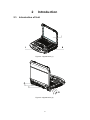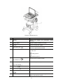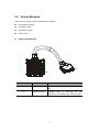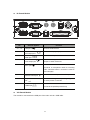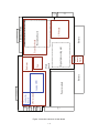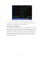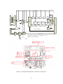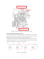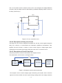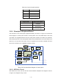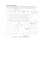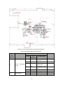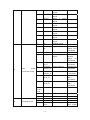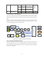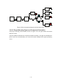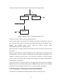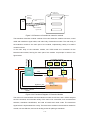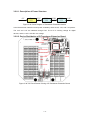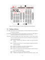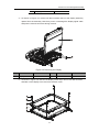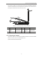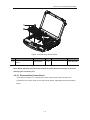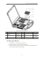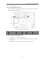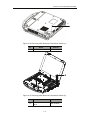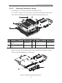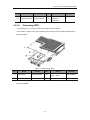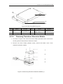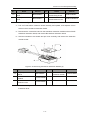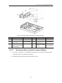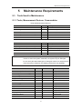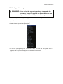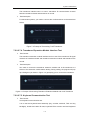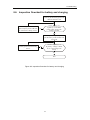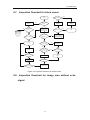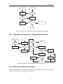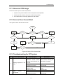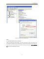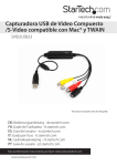
1
M5 Series Diagnostic Ultrasound System Service Manual Contents Contents .......................................................................................................... i Intellectual Property Statement .................................................................................... V Responsibility on the Manufacturer Party .................................................................... V Warranty ..................................................................................................................... VI Return Policy ............................................................................................................ VIII 1 System Overview .................................................................................. 1-1 1.1. Intended Use .................................................................................................. 1-1 1.2. Product and Model Code ................................................................................ 1-1 2 Introduction ........................................................................................... 2-1 2.1. Introduction of Unit .......................................................................................... 2-1 2.2. Extend Modules .............................................................................................. 2-3 2.3. Control Panel .................................................................................................. 2-5 3 Principle Description ............................................................................ 3-1 3.1. Electric Principle of the System ...................................................................... 3-1 3.2. Principle of Boards .......................................................................................... 3-2 3.2.1. Power System ........................................................................................ 3-2 3.2.2. Principle of Main Board .......................................................................... 3-9 3.2.3. Principle of Transmission Board ........................................................... 3-31 3.2.4. Principle of CW Board .......................................................................... 3-32 3.2.5. Principle of Keyboard Board ................................................................. 3-40 3.2.6. Principle of ECG Board ........................................................................ 3-47 3.2.7. Principle of Video/Audio Capture Card ................................................. 3-51 3.2.8. Principle of Transducer Extension Module ........................................... 3-52 3.3. Software Startup ........................................................................................... 3-55 4 Structure and Assembly/Disassembly ................................................ 4-1 4.1. Explosive Figure of the Complete System ...................................................... 4-1 4.2. Structure and Assembly/Disassembly ............................................................. 4-2 4.2.1. Removing Battery ................................................................................... 4-2 4.2.2. Removing Display Assembly .................................................................. 4-2 4.2.3. Removing Top cover main unit ............................................................... 4-7 i 4.2.4. Removing the Power Board ................................................................. 4-11 4.2.5. Removing Battery Connection Board ................................................... 4-14 4.2.6. Removing Continuous Wave Doppler Board ........................................ 4-15 4.2.7. Removing CPU Fan ............................................................................. 4-16 4.2.8. Removing CPU Board and Radiator Module ........................................ 4-18 4.2.9. Removing the System Fan ................................................................... 4-20 4.2.10. Removing Speakers ............................................................................. 4-21 4.2.11. Removing Transmission Board ............................................................ 4-22 4.2.12. Removing Main Board and Transducer Board ..................................... 4-23 4.2.13. Removing Transducer Board ................................................................ 4-25 4.2.14. Removing HDD .................................................................................... 4-26 4.2.15. Removing Transducer Extension Module ............................................. 4-27 4.2.16. Removing ECG Module........................................................................ 4-30 4.2.17. Removing Video and Audio Capture Module ........................................ 4-32 4.2.18. Removing Data Extension Module ....................................................... 4-34 4.2.19. Disassemble the Dust Net .................................................................... 4-34 5 Maintenance Requirements ................................................................. 5-1 5.1. Tools Used in Maintenance ............................................................................. 5-1 5.1.1. Tools, Measurement Devices, Consumables ......................................... 5-1 5.2. Maintenance Personnel .................................................................................. 5-2 6 Check ..................................................................................................... 6-1 6.1. Checking System Status ................................................................................. 6-1 6.1.1. Check Plan ............................................................................................. 6-1 6.1.2. Confirmation before Check ..................................................................... 6-1 6.2. Checking functions ......................................................................................... 6-2 6.2.1. Check Flowchart..................................................................................... 6-2 6.2.2. Checked Content.................................................................................... 6-2 6.3. Safety Check .................................................................................................. 6-3 6.3.1. Check of Electrical Safety ...................................................................... 6-3 6.3.2. Mechanical Safety Check ....................................................................... 6-3 6.4. Image Check ................................................................................................... 6-6 6.4.1. System Setup ......................................................................................... 6-6 6.4.2. Image Recording and Archiving ............................................................. 6-6 6.4.3. Check Flow ............................................................................................ 6-6 ii 6.4.4. Checking Phantom Data ........................................................................ 6-6 6.4.5. Final Operation Check and Image Archiving .......................................... 6-7 7 System Maintenance ............................................................................ 7-1 7.1. System Cleaning ............................................................................................. 7-1 7.1.1. Flow of Cleaning..................................................................................... 7-1 7.1.2. Details of Cleaning ................................................................................. 7-1 7.2. Software Maintenance .................................................................................... 7-3 7.2.1. Entering Preset....................................................................................... 7-4 7.2.2. Viewing System Information ................................................................... 7-4 7.2.3. Data Management .................................................................................. 7-5 7.2.4. Maintenance Status ................................................................................ 7-6 7.2.5. Software Upgrade .................................................................................. 7-7 7.2.6. Enter Windows ..................................................................................... 7-10 7.2.7. Model Setup ......................................................................................... 7-11 7.2.8. Installing Optional Software .................................................................. 7-12 7.2.9. System Self-diagnosis .......................................................................... 7-13 8 Troubleshooting .................................................................................... 8-1 8.1. Recover after the operating system is damaged ............................................. 8-1 8.2. Recover after the ultrasound software is damaged ......................................... 8-2 8.3. Recover after the patient database is damaged.............................................. 8-4 8.4. Recovering after HDD fails ............................................................................. 8-5 8.5. Inspection flowchart for power adapter and dc-dc circuit ................................ 8-7 8.6. Inspection flowchart for battery and charging ................................................. 8-8 8.7. Inspection flowchart for black screen .............................................................. 8-9 8.8. Inspection flowchart for image area without echo signal ................................. 8-9 8.9. Inspection flowchart for image with black area ............................................. 8-10 8.10. Abnormal Image in an Image ........................................................................ 8-10 8.11. Abnormal CW Image .................................................................................... 8-11 8.12. Service Flow Cannot Start ............................................................................ 8-11 8.13. Troubleshooting for PC System .................................................................... 8-11 8.14. Troubleshooting for CW board ...................................................................... 8-12 8.15. Troubleshooting for the keyboard board ....................................................... 8-13 8.16. Troubleshooting for ECG board .................................................................... 8-14 8.17. Troubleshooting for video & audio capture card............................................ 8-18 iii 8.18. Troubleshooting for transducer extension module ........................................ 8-18 Appendix A Interface Definition Index...................................................... A-1 Appendix B ELECTRICAL SAFETY INSPECTION.................................... B-1 iv ©2008-2010 Shenzhen Mindray Bio-Medical Electronics Co., Ltd. All rights Reserved. For this Operator’s Manual, the issue date is 2010-06. Intellectual Property Statement SHENZHEN MINDRAY BIO-MEDICAL ELECTRONICS CO., LTD. (hereinafter called Mindray) owns the intellectual property rights to this Mindray product and this manual. This manual may refer to information protected by copyright or patents and does not convey any license under the patent rights or copyright of Mindray, or of others. Mindray intends to maintain the contents of this manual as confidential information. Disclosure of the information in this manual in any manner whatsoever without the written permission of Mindray is strictly forbidden. Release, amendment, reproduction, distribution, rental, adaptation, translation or any other derivative work of this manual in any manner whatsoever without the written permission of Mindray is strictly forbidden. , WATO, BeneHeart, , , , , BeneView, are the trademarks, registered or otherwise, of Mindray in China and other countries. All other trademarks that appear in this manual are used only for informational or editorial purposes. They are the property of their respective owners. Responsibility on the Manufacturer Party Contents of this manual are subject to change without prior notice. All information contained in this manual is believed to be correct. Mindray shall not be liable for errors contained herein or for incidental or consequential damages in connection with the furnishing, performance, or use of this manual. V Mindray is responsible for the effects on safety, reliability and performance of this product, only if: z all installation operations, expansions, changes, modifications and repairs of this product are conducted by Mindray authorized personnel; z the electrical installation of the relevant room complies with the applicable national and local requirements; and z the product is used in accordance with the instructions for use. Upon request, Mindray may provide, with compensation, necessary circuit diagrams, calibration illustration list and other information to help qualified technician to maintain and repair some parts, which Mindray may define as user serviceable. Note This equipment is not intended for family usage. This equipment must be operated by skilled/trained medical professionals. Warning It is important for the hospital or organization that employs this equipment to carry out a reasonable service/maintenance plan. Neglect of this may result in machine breakdown or injury of human health. Warranty THIS WARRANTY IS EXCLUSIVE AND IS IN LIEU OF ALL OTHER WARRANTIES, EXPRESSED OR IMPLIED, INCLUDING WARRANTIES OF MERCHANTABILITY OR FITNESS FOR ANY PARTICULAR PURPOSE. Exemptions Mindray's obligation or liability under this warranty does not include any transportation or other charges or liability for direct, indirect or consequential damages or delay resulting from the improper use or application of the product or the use of parts or accessories not approved by Mindray or repairs by people other than Mindray VI authorized personnel. This warranty shall not extend to: z Any Mindray product which has been subjected to misuse, negligence or accident; z Any Mindray product from which Mindray's original serial number tag or product identification markings have been altered or removed; z Any product of any other manufacturer. Safety, Reliability and Performance Mindray is not responsible for the effects on safety, reliability and performance of the product if: z Assembly operations, extensions, re-adjusts, modifications or repairs are carried out by persons other than those authorized by Mindray. z Personnel unauthorized by Mindray repairs or modifies the instrument. VII Return Policy Return Procedure In the event that it becomes necessary to return this product or part of this product to Mindray, the following procedure should be followed: 1. Obtain return authorization: Contact the Mindray Service Department and obtain a Customer Service Authorization (Mindray) number. The Mindray number must appear on the outside of the shipping container. Returned shipments will not be accepted if the Mindray number is not clearly visible. Please provide the model number, serial number, and a brief description of the reason for return. 2. Freight policy: The customer is responsible for freight charges when this product is shipped to Mindray for service (this includes customs charges). 3. Return address: Please send the part(s) or equipment to the address offered by Customer Service department Company Contact Manufacturer: Shenzhen Mindray Bio-Medical Electronics Co., Ltd. Address: Mindray Building, Keji 12th Road South, Hi-tech Industrial Park, Nanshan, ShenZhen 518057, P. R. China Tel: +86 755 26582479 26582888 Fax: +86 755 26582934 26582500 EC-Representative: Address: Tel: Fax: Shanghai International Holding Corp. GmbH(Europe) Eiffestraβe 80, Hamburg 20537, Germany 0049-40-2513175 0049-40-255726 VIII Safety Precautions 1. Meaning of Signal Words In this operator’s manual, the signal words DANGER, WARNING, CAUTION and NOTE are used regarding safety and other important instructions. The signal words and their meanings are defined as follows. Please understand their meaning before reading this manual. Signal word Meaning DANGER Indicates an imminently hazardous situation that, if not avoided, will result in death or serious injury. WARNING Indicates a potentially hazardous situation that, if not avoided, could result in death or serious injury. CAUTION Indicates a potentially hazardous situation that, if not avoided, may result in minor or moderate injury. Indicates a potentially hazardous situation that, if not avoided, may result in property damage. NOTE 2. Meaning of Safety Symbols Symbol Description Type-BF applied part The ultrasound transducers connected to this system are Type-BF applied parts. The ECG module connected to this system is Type-BF applied part. "Attention" indicates the points that you should pay attention to. Be sure to read the operator’s manual concerning these points before using the system. IX 3. Safety Precautions Please observe the following precautions to ensure patient’s and operator’s safety when using this system. DANGER: Do not use flammable gasses, such as anesthetic gas, oxygen or hydrogen, or flammable liquids such as ethanol, near this system, because there is danger of explosion. WARNING: 1 Connect the adapter power plug of this system and power plugs of the peripherals to wall receptacles that meet the ratings indicated on the rating nameplate. Using a multifunctional receptacle may affect the system grounding performance, and cause the leakage current to exceed safety requirements. You must use the power adapter provided with the system; otherwise electric shock may result. 2 Use the printing cable provided with this system to connect the printer. Electric shock may result. 3 Connect the grounding conductor before turning ON the system. Disconnect the grounding cable after turning OFF the system. Otherwise, electric shock may result. 4 For the connection of power and grounding, follow the appropriate procedures described in this operator’s manual. Otherwise, there is risk of electric shock. Do not connect the grounding cable to a gas pipe or water pipe; otherwise improper grounding may result or a gas explosion may occur. 5 Before cleaning the system, disconnect the power cord from the outlet. System failure and electric shock may result. 6 This system is not water-proof. Do not use this system in any place where water leakage may occur. If any water is sprayed on or into the system, electric shock may result. If water is accidentally sprayed on or into the system, contact Mindray Department or sales representative. X Customer Service 7 Store and use the transducers carefully. Do not use a transducer that has a damaged, scratched surface, or exposed wiring of any kind. Immediately stop using the transducer and contact Mindray Customer Service Department or sales representative. 8 Do not allow the patient to contact the live parts of the ultrasound system or other devices, e.g. signal I / O ports. Electric shock may occur. 9 Do not use an aftermarket transducer other than those specified by Mindray. The transducers may damage the system causing a profound failure, e.g. a fire in the worst case. 10 Do not subject the transducers to knocks or drops. Use of a defective transducer may cause an electric shock. 11 Do not open the covers and front panel of the system. Short circuit or electric shock may result when the system hardware is exposed and powered on. 12 Do not use this system simultaneously with equipment such as an electrosurgical unit, high-frequency therapy equipment, or a defibrillator, etc.; otherwise electric shock may result. 13 If the grounding wire is questionable, you should disconnect the system from the supply power and stop using the adapter, and change the power supply to internal batteries. 14 Only use the ECG leads provided with the ECG module; otherwise electric shock may result. 15 When moving the system, you should first fold the LCD display, disconnect the system from other devices (including transducers) and disconnect the system from the power supply. 16 Accessory equipment connected to the analog and digital interfaces must comply with the relevant IEC standards (e.g., IEC 60950 information technology equipment safety standard and IEC 60601-1 medical equipment standard). Furthermore all configurations must comply with the standard IEC60601-1-1. It is the responsibility of the person, who connects additional equipment to the signal input or output ports and configures a medical system, to verify that the system complies with the requirements of IEC60601-1-1. If you have any questions regarding these requirements, consult your sales representative. XI 17 Prolonged and repeated use of keyboards may result in hand or arm nerve disorders for some individuals. Observe the local safety or health regulations concerning the use of keyboards. CAUTION: 1 Precautions concerning clinical examination techniques: a) This system must be used only by qualified medical professionals. b) This operator’s manual does not describe clinical examination techniques. The clinician should select the proper examination techniques based on specialized training and clinical experience. 2 Malfunctions due to radio wave: a) If a radio wave emitting device is used in the proximity of this system, it may interfere with operations. Do not bring or use devices that generate radio waves, such as cellular telephones, transceivers, and radio controlled toys, in the room where the system is installed. b) If a person brings a device that generates radio waves near the system, ask him / her to immediately turn OFF the device. 3 Precautions concerning movement of the system: a) When you place the system on the mobile trolley and move them together, you must secure all objects on the mobile trolley to prevent them from falling. Otherwise you should separate the system from the mobile trolley and move them individually. When you have to move the system with the mobile trolley upward or downward the stairs, you must separate them first and then move them individually. b) Object placed on the monitor may fall and injure an individual. c) Fasten and fully secure any peripheral device before moving the system. A loose peripheral device may fall and injure an individual. 4 Do not expose the system to excessive vibration through transportation. Mechanical damage may result. XII 5 Do not connect this system to outlets with the same circuit breakers and fuses that control the current of devices such as life-support systems. If this system malfunctions and generates overcurrent, or when there is an instantaneous current at power ON, the circuit breakers and fuses of the building’s supply circuit may be tripped. 6 Always keep the system dry. Avoid transporting this system quickly from a cold place to a warm place; otherwise condensation or water droplets may form allowing a short circuit and possible electric shock. 7 If the circuit protector is tripped, it indicates that the system or a peripheral device was improperly shut down and the system is unstable. You cannot repair the system under this circumstance and must call the Mindray Customer Service Department or sales representative. 8 There is no risk of high-temperature burns during routine ultrasound examinations. It is possible for the surface temperature of the transducer to exceed the body temperature of a patient due to environmental temperature and exam type combinations. If a patient complains of any excessive heat from the transducer, immediately stop scanning. To prevent patient burns, ensure there is no surface damage to the transducer. Do not apply the transducer to the same region on the patient for a long time. Apply the transducer only for a period of time required for the purpose of diagnosis. 9 The system and its accessories are not disinfected or sterilized prior to delivery. The operator is responsible for the cleaning and disinfection of transducers and sterilization of biopsy brackets according to the manuals, prior to the use. All items must be thoroughly processed to completely remove harmful residual chemicals or gasses that are harmful to the human body or that may damage the accessory. 10 It is necessary to press [End Exam] to end the current scan that is in progress and clear the current Patient Information field. Otherwise new patient data may be combined with the previous patient data. XIII 11 Do not connect or disconnect the system’s power cord or its accessories (e.g., a printer or a recorder) without turning OFF the power first. This may damage the system and its accessories or cause electric shock. 12 Do not turn OFF the power supply of the system during printing, file storage or invoking other system operations. An interrupted process may not be completed, and can become lost or corrupted. 13 If the system is powered off improperly during operation, it may result in data damage of the system’s hard disk or system failure. 14 Do not use the system to examine a fetus in the Doppler mode for a long period of time. 15 Do not use a USB memory device (e.g., a USB flash drive, removable hard disk) which has unsafe data. Otherwise system damage may result. 16 It is recommended to only use the video devices specified in this manual. NOTE: 1 Do not use the system in the vicinity of strong electromagnetic field (such as a transformer), which may affect the performance of the system. 2 Do not use the system in the vicinity of high-frequency radiation source, which may affect the performance of the system or even lead to failure. 3 To avoid damaging the system, do not use it in following environment: a) Locations exposed to direct sunlight; b) Locations subject to sudden changes in environmental temperature; c) Dusty locations; d) Locations subject to vibration; e) Locations near heat generators; f) Locations with high humidity. 4 Turn ON the system only after the power has been turned OFF for more than 20 seconds. If the system is turned ON immediately after being turned OFF, the system may not reboot properly and could malfunction. 5 Do not disconnect a transducer that remains in a live imaging state. This can damage the system and / or transducer. Press [Freeze] or turn off the power of the system before connecting or disconnecting a transducer. XIV 6 Remove ultrasound gel from the face of a transducer when the examination is complete. Water in the gel may enter the acoustic lens and adversely affect or damage the transducer array and lens. 7 You should properly back up the system to a secure external storage media, including system configuration and settings and patient data. Data stored to the system’s hard drive may be lost due to system failure, improper operation or accident. 8 Do not apply external force to the control panel. The system may be damaged. 9 If the system is used in a small room, the room temperature may rise. Provide proper ventilation and free air exchange. 10 To dispose of the system or any part, contact Mindray Customer Service Department or sales representative. Mindray is not responsible for any system content or accessories that have been discarded improperly. 11 To ensure optimal system operations, it is recommended that you maintain the system under a Mindray service agreement. Various aspects of system performance and operation can be maintained under the professional supervision of a service representative. 12 The iScape feature constructs a single extended image from a series of individual image frames. The quality of the final image is user-dependent and requires skill to efficiently apply the feature and technique. Exercise caution when measurements are performed from an iScape image. 13 Ensure that the current exam date and time are the same as the system date and time. 4. Warning Labels The warning labels are attached to this system in order to call your attention to potential hazards. The symbol on the warning labels indicates safety precautions. The warning labels use the same signal words as those used in the operator’s manual. Refer to the operator’s manual for detailed information about the warning labels. Read operator’s manual carefully before using the system. The name, pattern and meaning of each warning label are described as follows: XV No. Label Meaning a) Before using the system, be sure to carefully read the relevant content of this operator’s manual. b) Do not place any object on the keyboard; beware of excessive stress exerted to the keyboard; fold the keyboard when moving the system. c) DANGER: There is explosion risk if the system is used with flammable anesthetics. <1> a) <2> b) a) Before using the system, be sure to carefully read the relevant content of this operator’s manual. The following labels are available when the system works with the mobile trolley. a) 5. c) b) b) CAUTION: Do not place the system with the mobile trolley on a sloped surface. Otherwise the system may slide, resulting in personal injury or the system malfunction. Two persons are required to move the system over a sloped surface. c) CAUTION: Do not sit on the system. c) Symbol Explanation Symbol Name / ON/OFF Power button ETHERNET Network port PARALLEL Parallel port SERIAL REMOTE USB AUDIO S-VIDEO VIDEO XVI Function Serial port Remote control port USB port Audio signal S-VIDEO signal interface VIDEO signal interface VGA RGB PROBE Mic IO extend VGA signal RGB signal Transducer port Microphone input jack IO extend port / Battery status indicator / Battery installation position indicator / Pencil probe port / Locking a transducer / Unlocking a transducer / Connecting power supply / Power adapter port / Product serial number / Manufacture date XVII System Overview 1 System Overview 1.1. Intended Use The M5/M5T system is intended for use in ultrasound exams for human. There is one difference between M5T and M5, that is, M5 has a pediatric measurement package, but M5T does not. The M5Vet system is intended for use in ultrasound exams for animals. 1.2. Product and Model Code M □ □ Vet: Veterinary use Model code Product code 1-1 2 Introduction 2.1. Introduction of Unit Figure 2-1 Appearance (1) Figure 2-2 Appearance (2) 2-1 Figure 2-3 Appearance (3) No Name Function 1 Monitor Displays the images and parameters during scanning 2 Control panel Operator-system interface or control 3 Handle Used for carrying the system 4 Transducer port Connects a transducer to the main unit; or connects a probe extend module 5 Transducer locking lever Locks or unlocks the transducer connected with the main unit : locking symbol : unlocking symbol 6 Connects the IO extend module IO extend port 7 Power input port Connects the power adapter 8 USB port Connects USB devices 9 Network port Connects the network 10 S-Video separate video output Connects VCR recorder or video printer 11 Mobile trolley Optional device, used for placing the ultrasound system and extend modules 2-2 2.2. Extend Modules There are four extend modules available for the system: Probe extend module IO extend module V/A extend module ECG module z Probe Extend Module <1> <2> No Name Function <1> Connector Connects to the transducer port of the main unit <2> Transducer ports Extended ports for connecting two live transducers; the middle one is a docking port 2-3 z IO Extend Module No <1>, <2> Name & Symbol USB port Function Connects USB devices. Connects a display or projector <3> VGA output port <4> <5>, <6> <7> Serial port Connects serial port devices Audio output port Used for audio signals of PW sound from DVD output or audio comments Mic In port Reserved (Connects a microphone used for receiving audio comments when a recorder is used to record images) <8> <9> <10> z Remote control port Connects the control port of the video printer Composite video output Used for receiving the output image signal of the video printer or recorder port Parallel port Reserved. (Connects the parallel port devices) V/A Extend Module The module is connected to the USB port of the main unit via a USB cable. 2-4 No z < 3> <2> < 1> Name <4> Function <1> Audio input port Used for audio signal input <2> Audio input port Used for audio signal input <3> Composite video input port Used for composite signal video input <4> Separate video input port Used for separate signal video input ECG Module The module is connected to the USB port of the main unit via a USB cable. Name ECG lead port Function Used for ECG signal input 2.3. Control Panel 2-5 No <1> / English Name Name Description soft controls 1 Function menu Press to select the soft menu items displayed on the bottom of the screen. Refer to the subsequent contents for specific functions. <2> / soft controls 2 menu Press to select the soft menu items displayed on the bottom of the screen. Refer to the subsequent contents for specific functions. <3> / soft controls 3 menu Press to select the soft menu items displayed on the bottom of the screen. Refer to the subsequent contents for specific functions. <4> / soft controls 4 menu Up / down controls are used to turn pages up / down when there are more-than-one pages for the soft menu; Left / right controls are used to switch between the exam types. 2-6 <5> / soft menu Press to select the soft menu items displayed controls 5 on the bottom of the screen. Refer to the subsequent contents for specific functions. <6> / soft menu Press to select the soft menu items displayed controls 6 on the bottom of the screen. Refer to the subsequent contents for specific functions. <7> / Power button When you press the power button to turn on the system, the system enters the work status and the indicator lights on and becomes green. When the system enters the standby status, the indicator turns yellow. When you press the power button to turn off the system, the indicator lights off. <8> Esc Escape Press to exit the current status to the previous status. <9> Help Help Press to open or close the accompanying help documents. <10> Report Report Press to open or close the diagnosis reports. <11> / Press to enter or exit the patient information iStation management system. <12> F1 User-defined key You can assign a function to the key. <13> F2 User-defined key You can assign a function to the key. <14> F3 User-defined key You can assign a function to the key. <15> F4 User-defined key You can assign a function to the key. <16> Quad 4-split screen Press to enter or exit the 4-split screen display. display <17> Biopsy Biopsy Press to show or hide the biopsy guide line. <18> Setup Setup Press to show or hide the Setup menu. <19> Del Delete Press to delete the comment, etc. <20> / Alphanumeric Same as those of PC. keys <21> Menu Menu Press to display a mode-specific parameter menu and / or access other system selections. <22> TGC <23> Comment Time Gain Move to adjust time gain compensation. Compensation Comment Press to enter or exit the character comment status. 2-7 <24> Arrow Arrow Press to enter or exit the arrow comment status. <25> Clear Clear Press to clear the comments or measurement calipers on the screen. <26> Info Patient Press to enter the patient information input information screen. <27> Exam Exam type Press to switch between exam types. <28> Review Review Press to review the image files stored. <29> End Exam End exam Press to end an exam. <30> Body Mark Body mark Press to enter or exit the Body Mark status. <31> Cine Cine review Press to enter or exit the Cine Review status. <32> Zoom Zoom Press to enter or exit the Zoom status. <33> Back <34> Change Return or delete Change Press to return to the previous operation or delete the previous item. Press to toggle between calipers within the same measurement. <35> <36> <37> Measure Measure Caliper Caliper Set Set Press to enter or exit the application measurement mode. Press to enter or exit the general measurement mode. Press to confirm an operation, same as the left-button of the mouse. <38> / Trackball Roll the trackball to move the cursor position. <39> / Multifunction Rotate to adjust image parameters or comment knob arrows. <40> B / Press to enter the B mode <41> Dual / Press to enter the Dual mode from another mode; Press to switch between the two display windows in the Dual mode. <42> iTouch / Rotate to increase or decrease the image gain; press to optimize the image, serving as a one-key optimization. <43> Color / Press to enter the Color mode. <44> Power / Press to enter the Power mode. <45> CW / Reserved for the CW mode. <46> Update / Press to change the current window if there are more-than-one windows. 2-8 <47> PW / Press to enter the PW mode. <48> M / Press to enter the M mode. <49> Print Print Press to print the contents which are set. <50> Save Save Press to save the single-frame images in the preset format. <51> Depth Depth Press to increase or decrease the imaging depth. <52> Freeze Freeze Press to freeze or unfreeze onscreen image. <53> / Indicator 1 Indicates if the main unit is connected to the power supply. When the main unit is not connected to the power supply, the indicator light is off. When the main unit is connected to the power supply, the indicator light is on and in green color. <54> / Indicator 2 Indicates the current status of the batteries. When the system is supplied with power by the batteries and the power capacity is lower than 30%, the indicator is yellow and flashes. When the batteries are being charged, the indicator light is on and in yellow color. When the battery capacity is charged to the full capacity, the indicator color changes from yellow to green. In other statuses, the indicator light is off. There are five keys which can work with the Fn key: Key Name Function [Fn] + Press the two keys to increase the brightness of the LCD display. [Fn] + Press the two keys to decrease the brightness of the LCD display. [Fn] + [S] [Fn] + [Fn] + Press the two keys to mute the speaker. Press the two keys to increase display contrast. Press the two keys to decrease display contrast. 2-9 3 Principle Description 3.1. Electric Principle of the System The M5 system is a compact color ultrasound imaging system. Its schematic diagram is shown in Figure 3-1 Trans ducer A (Live) I/O Extension Board Trans ducer B Trans ducer C (Live) Transducer Extension Board Transducer LCD CPU Board AD Board Transducer Board 4D Driver Board USB ECG Module Master Board USB USB Footswitch PC System USB USB Video Collection Module PCI Ultrasound System Transmitter Board USB Control Panel Board Power & LED Control CW Board L_Speaker Pencil Probe R_Speaker Power Supply Board Battery Connection Board EDC Main unit Battery Figure 3-1 Schematic Diagram The M5 system consists of main unit, peripheral extension modules and power system. The main unit contains the following parts. z Master Board: ultrasound system: used for ultrasound echo reception, amplification, sampling, beam forming, signal processing, ultrasound scan receiving control and data communications between PC system. PC system: used for post processing of echo data, interaction with the user, and supporting peripherals. Power management and filter system: used for ensuring normal work of system power, supporting normal turn-off, standby and dormant status. In addition, the Master Board provides connecting ports for modules. z Transmitter Board: used for delay focusing transmission. 3-1 z Control Panel Board: used for communicating with the Master Board via USB port, supporting keyboard control before the PC system is initiated. z z CPU Board: used for PC system Transducer Board: used for connecting transducers or transducer extension module. z 4D Driver Board (reserved) z CW Board: used for analog CW signal processing and pencil probe signal processing. The extension modules include: z Transducer Extension Board: used for supporting 3 transducer ports; only two of them are live. z I/O Extension Board z USB ECG Module z USB Footswitch z USB Video Capture Module: used for video collection via USB port. z L_Speaker & R_Speaker: left speaker and right speaker. Power system (including power management and filter system on the Master Board): z Power Supply Board: used for supplying power for the ultrasound system. z Battery Connection Board z Battery z EDC(External Direct Current): external power adapter. 3.2. Principle of Boards 3.2.1. Power System 3.2.1.1. Basic Functions The power system is used to supply power for the ultrasound system, and it consists of power adapter, batteries, battery connection board, main and auxiliary power boards. The power is supplied through two methods, external power adapter or batteries. The system is first powered by the adapter, and the batteries are provided for back-up. The main and auxiliary power boards are used to provide direct current output and charging management. Table 3-1 DC Power Output No 1 2 3 4 5 Output +12V 5Vstb 5Vstb_CPU +5V +3.3V Name of Boards Main power board Main power board Main power board Main power board Main power board 3-2 Remark controlled by power_on signal Output for all time controlled by 5Vstb_CPU_EN signal controlled by power_on signal controlled by power_on signal 6 THV 7 +2.5V 8 +1.5V 9 -5V 10 -12V Main power board Auxiliary power board Auxiliary power board Auxiliary power board Auxiliary power board controlled by power_on signal controlled by power_on signal controlled by power_on signal controlled by power_on signal controlled by power_on signal 3.2.1.2. Principle of Power System As shown in Figure 3-2, after the batteries and adapter are connected to the system main board, the main power board is connected through a 64-pin socket, generating outputs of +12v, +5v, 5Vstb, 5Vstb_cpu, +3.3V, and THV. The Vbus+, +5v, and EDC_Power signals are inputted to the auxiliary power board through the main power board via the 26-pin socket. In the auxiliary power board, the -12V, -5V, +2.5V, and +1.5V are obtained, and charging management is implemented. The 64-pin socket and 26-pin socket signal definitions are shown in Table 3-2 Signal Definition of Connectors between Main Power Board and System Main Board and Table 3-3 Signal Definition of Connectors between Main Power Board and Auxiliary Power Board. 3-3 Pow er in Edc_pow er Edc_pow er Edc_pow er A _B A T T ER Y _N T C A _B A T T ER Y _N T C B _B A T T ER Y _N T C B _B A T T ER Y _N T C Pow er_on Scan_status C W _m ode 5V stb_cpu_en A dapter Pow er_on Scan_status T H V _range start T EM P_D + T EM P_D - System m ain board C ontrolSignal A _B A T T ER Y + B attery pack A V B U S+ + 5V + 5V + 5V stb + 5V stb_cpu M ain pow er board A uxiliary pow er board + 3.3V TH V C ontrolSignal A _B A T T ER Y + + 2.5V + 2.5V + 1.5V + 1.5V - 5V - 5V - 12V - 12V A _B A T T ER Y + A _B A T T ER Y + B _B A T T ER Y + B _B A T T ER Y + B _B A T T ER Y + C ontrolSignal B attery connect board B _B A T T E R Y + + 12V B attery pack B Figure 3-2 Schematic Diagram of Power System Table 3-2 Signal Definition of Connectors between Main Power Board and System Main Board Pin No. 1 Name EDC_Power Pin No. 2 Name EDC_Power 3 EDC_Power 4 EDC_Power 5 GND 6 GND 7 GND 8 GND 9 A_Battery+ 10 A_Battery+ 3-4 11 A_Battery- 12 A_Battery- 13 B_Battery+ 14 B_Battery+ 15 B_Battery- 16 B_Battery- 17 Gnd 18 Gnd 19 A_Battery_NTC 20 B_Battery_NTC 21 EDC_Status 22 Power_ON 23 Gnd 24 Scan_Status 25 Temperature_D+ 26 CW_Mode 27 Temperature_D- 28 +5VStb_CPU_En 29 Gnd 30 Gnd 31 +5VSTB 32 +5Vstb_CPU 33 +12V 34 +12V 35 GND 36 GND 37 GND 38 GND 39 -5.3V 40 -12V 41 Gnd 42 Gnd 43 +5V 44 +5V 45 Gnd 46 Gnd 47 +2.5V 48 +2.5V 49 Gnd 50 Gnd 51 Gnd 52 +1.5V_Feedback 53 +1.5V 54 +1.5V 55 Gnd 56 Gnd 57 +3.3V 58 +3.3V 59 Gnd 60 Gnd 61 Gnd 62 Gnd 63 THV 64 THV_Range Table 3-3 Signal Definition of Connectors between Main Power Board and Auxiliary Power Board Pin No. 1 Name GND Pin No. 2 Name -5.3V 3 Scan_status 4 -12V 5 Power_on 6 +2.5V 7 B_Battery_NTC 8 +2.5V 9 A_Battery_NTC 10 Gnd 11 Gnd 12 Gnd 13 B_Battery+ 14 1.5V_feedback 15 A_Battery+ 16 +1.5V 17 Edc_power 18 +1.5V 19 GND 20 GND 21 GND 22 GND 23 Vbus+ 24 +5VL 25 GND 26 Start 3-5 3.2.1.3. 5vstb Circuit Unit 3.2.1.3.1. Principle of 5vstb The relation between the adapter output Edc_power and battery output batt is “OR”. After “Edc_power” or “batt”, as being input of 5vstb, goes through the linear stablizing chip MIC5202-5.0YMS, the 5vstb is obtained. The overcurrent and overtemperature protection is implemented in MIC5202-5.0YMS. 3.2.1.3.2. Service Points for 5vstb If the 5vstb unit is faulty, first check if the input voltage of U9 PIN1 is normal; if normal, it indicates that the U9 is damaged or the fault is caused by the overcurrent or shortcircuit of the load. 3.2.1.4. +12v circuit unit 3.2.1.4.1. Principle of +12v The rise-and-fall voltage chip LTC3780EG#PBF made by Linear company is adopted for the +12v circuit unit. Whether the input voltage is lower or higher than 12v, the output voltage is stablized at 12v. The +12v overcurrent and overvoltage protection is not locked, and the overcurrent is between 6.5A and 9.5A. The output voltage returns to normal after overcurrent disappears. 3.2.1.4.2. Service Points of +12v Before testing, ensure that the power_on signal is low level and the input voltage VBUS+ is normal. The work flow of service is shown as follows: • Measure the level of U3 PIN8, which should be higher than 4V; • Measure the level of U3 pin19, which should be about 6v; • Use an oscilloscope to measure G poles of Q11, Q18, Q24 and Q25 to check if there is drive pulse; at least two MOSs’ G poles have drive pulse; • Check if four MOSs’ Q11, Q18, Q24 and Q25 and diode D5 and D7 are damaged. 3.2.1.5. Circuit Units of +5v and +3.3v 3.2.1.5.1. Principle of +5v and +3.3v The implementations of +5v and +3.3v are the same. The chip LTM4600 made by Linear company is adopted for the two circuit units. This chip is a step-down and synchronous-rectification IC, and it is incorporated with two MOS semiconductors and power inductor. LTM4600 is incorporated with overcurrent protection. 3.2.1.5.2. Service Points of +5v and +3.3v Before testing, ensure that +12v output is normal and the input voltage VBUS+ is normal. 3-6 The work flow of service is shown as follows: • Test PIN23, which should be high level; • Check if R6 (+3.3v unit) and R12 (+5v unit) are well soldered; • Check if the soldering position IC is proper, if not, it will cause short circuit of pins at the bottom of the IC. 3.2.1.6. THV Circuit Unit 3.2.1.6.1. Principle of THV THV consists of a step-down circuit and a step-up circuit. The step-down circuit outputs 5~ 10v (the voltage value is controlled by THV_range, 0v corresponding to THV’s 5v, 4v corresponding to THV’s 10V). The step-up circuit outputs 20~140v (the voltage value is controlled by THV_range, 0v corresponding to THV’s 20v, 4v corresponding to THV’s 140V). The step-down circuit is always at the working status. The step-up circuit is controlled by cw_mode; when the cw_mode is low, the step-up circuit is at the working status. The step-down control chip u10 is TPS54350, incorporating a MOS semiconductor. The step-up control chip U2 is TL594. Between the step-up circuit input and +12v is P-MOS semiconductor U6. The step-down circuit does not have overvoltage protection. The step-up circuit (20V~ 140V) has overvoltage protection, and the overvoltage point is about 170v; the overvoltage is not locked; when overvoltage occurs, the voltage remains at about 170v. The step-up and step-down circuits both have overcurrent protection respectively, so when either has overcurrent, both circuits will stop working and be locked. 3.2.1.6.2. Service Points of THV circuit unit Before testing, ensure that +12v output is normal and negative pressure output of U1 is normal. The low voltage circuit and high voltage circuit are independent. First confirm whether overcurrent or shortcircuit causes thv circuit protection by means of ocp signal (when overcurrent occurs, the ocp signal is high level). After you confirm it is not caused by overcurrent or shortcircuit, check if it is caused by failure of low voltage circuit or high voltage circuit. If it is caused by low voltage circuit, check if U10 (TPS54350), U7, D1, R142, or R143 works normally. If it is caused by high voltage circuit, check if U6 (TL594), U2, Q5, D9, R110, or R111 works normally. The work flow of troubleshooting for U10 and its peripheral circuit is shown as follows: • Test PIN7, which should be higher than 0.5v; • Test PIN12, which should be about 8v; 3-7 • Test PIN16, which should be 8v higher than the voltage of PIN15; • Test PIN14 and PIN15, which should have pulse voltage waveform. The work flow of troubleshooting for U6 and its peripheral circuit is shown as follows: • Before testing, ensure that the cw_mode is low level, that is, the system is at the status of high voltage circuit; • Test PIN8 and PIN11, which should be 12v; • Test PIN14, which should be +5v; • Test PIN5, which should have oscillating waveform; • Test PIN15, which should be about 1.6v; • Test PIN9 and PIN10, which should have drive pulse. 3.2.1.7. Circuit Units of +2.5v and +1.5V 3.2.1.7.1. Principle of +2.5V and +1.5V The implementations of +2.5v and +1.5v are the same. The synchronous rectification and step-down chip EL7566 is adopted for both circuits. This chip is reliable and has low fault rate. The EL7566 is incorporated with overcurrent protection, and is not locked when overcurrent occurs. After the overcurrent disappears, output returns to normal. 3.2.1.7.2. Service Points of +2.5V and +1.5V Before power on, check if peripheral devices of EL7566 are well soldered, and check if the pins of EL7566 are well soldered or short circuited. After power on, refer to the work flow shown as follows: • Test PIN19~PIN21, which should be +5V; • Test PIN22, which should be +5V; • Test PIN27, which should have oscillating waveform; • Test PIN8~PIN13, which should have pulse voltage waveform. 3.2.1.8. Circuit Units of -5v and -12V 3.2.1.8.1. Principle of -5V and -12V The implementations of -5V and -12V are the same. The negative pressure Max1847 is adopted for both circuits. The -5V and -12v both have overvoltage and overcurrent protection circuits, so when either has overvoltage or overcurrent, both circuits will be off and locked. 3.2.1.8.2. Service Points of -5V and -12V Ensure that VBUS+ for -5V and -12v is within normal range. After power on, refer to the work flow shown as follows: • Test the PIN15 of power chip, and its voltage should be the same as that of VBUS+; 3-8 • Test PIN5 of reference voltage, which should be 1.25V; • Test PIN8 of overvoltage and overcurrent protection, which should be higher than 0.5v; • Test PIN14 of the drive, which should have drive pulse output. 3.2.1.9. Charging Unit 3.2.1.9.1. Principle of Charging Unit The rise-and-fall charging chip max1870 made by Maxim is adopted for both charging units A and B. The max1870 enbling is controlled by the system’s main board and battery’s temperature, and eventually controlled by level of PIN15. When PIN15 is high level (about 5v) the charging is enabled; when PIN15 is low level, the charging is not enabled. 3.2.1.9.2. Service Points of Charging Unit Before testing, ensure that the charging chip is enabled, that is, PIN15 is high level. The work flow is shown as follows: 1. Check if the soldering position departs from normal position, if so, it will cause short circuit of pins. 2. Test power supplying voltage PIN32, which should be equal to adapter’s output voltage of edc_power. 3. Test reference end’s PIN2, which should be about 4.0v. 4. Test linear stabilizing output PIN1, which should be 5.4V. 5. Test drive’s PIN27 and PIN22, at least either PIN has drive pulse output. 6. Test if the power device MOS semiconductor and diode are damaged. 3.2.2. Principle of Main Board The schematic diagram of the main board is shown in Figure 3-3. 3-9 Transducer board 4D port 1 Main board Beamforming Ultrasound reception CW port 1 Power connect board port CW port 2 Signal processing FPGA2 FPGA1 Transmit board 4D port 2 Main board power Temper ature sensor Fan port Video processing FPGA3 System detection multifunction Keyboard port Extension port Power port Adapter port Power manage ment COME INTERFACE USB port HDD port AD controller board Audio module Network board display Figure 3-3 Schematic Diagram of Main Board From the Figure 3-3, you can see that the main board consists of the following modules: ¾ Ultrasound reception ¾ Signal processing ¾ Power management ¾ System detection ¾ Video processing ¾ Back-end interface 3-10 The main board provides the interfaces for: ¾ Transducer board ¾ Transmit board ¾ CW board ¾ 4D board ¾ keyboard ¾ battery connecting board ¾ CPU module ¾ AD controller board ¾ power board ¾ HDD ¾ reserved power interface ¾ reserved signal interface ¾ fan ¾ speaker External interfaces include: ¾ S_Video ¾ network ¾ USB (two) ¾ Extension interface The above-mentioned module interfaces in the main board are shown in Figure 3-4. 3-11 Figure 3-4 Module interfaces of Main Board 3-12 Inlet fan SVIDEO Networ k port Dual USB port Adapter port ) Battery Laptop HDD Power module CPU module AD controller board Extension port Battery connect board Battery CW board Transmit board Reception board Signal processing unit Main board Fan Radiator Transducer board Transducer port Inlet fan Pencil probe port 3.2.2.1. Power Distribution M5’s power distribution is a big network. Refer to Figure 3-5 Power Distribution for reference. AMPLIFILER CPU CW_BOARD J16( reserved) +12V Power transform EMIT IDE, Au-amp, Aud-dec, USB, KeyBoard, Spp, J16, CW_BOARD +5V Power transform HVISO +4.7V +3.3V Power transform +3.3V Power transform +3.3V FPGA_BF FPGA,KeyBoard, Video-encode,Pull-Up,245,Auddec ADC( LVDD, AVDD) , PLD_REV, +5Vstb Power transform +3V VCA8617 Power transform +1.8V CPLD_REV Power transform +2.5V FPGA_BF Power transform +3.3V Pwr_CPLD +1.8V Board voltage Power transform +5Vstb For cpu -12V -5V CPU CW_BOARD Audio-amp CW_BOARD Power transform HVISO -4.7V Power transform +2V5 MMF 2996 FPGA_DSP DDR MMF_VTT MMF_VREF DDR0 2996 VTT 0 VTT1 2996 VTT 1 VTT1 +1.5V Power transform PHV EMITBOARD CWBOARD +1.2V DDR1 MMF,FPGA_DSP FPGA_BF Figure 3-5 Power Distribution 3-13 -3.3V Receive Receive 3.2.2.2. Ultrasound Reception The ultrasound reception consists of high voltage isolation and reception channel selection, voltage-controlled gain amplifier and ADC. The reception channel selection is implemented through two CPLDs. The analog control voltage of the voltage-controlled gain amplifier is derived from a DAC, and the SPI control signals of DAC and amplifier are both derived from FPGA1, likewise the ADC’s SPI control signal is derived from FPGA1. 3.2.2.3. Signal Processing The signal processing is implemented through two FPGAs: FPGA1 and FPGA2. The FPGA1 implements control of the front-end chips (such as channel selection CPLD, VGA gain control DAC, ADC, transducer and transducer extension module), generation of transmission sequence pulse, beamforming, and orthogonal demodulation. The FPGA2 implements signal processing, data uploading, loading of real time scan parameters, and data uploading through PCI interface. 3.2.2.4. Power Management Power management is implemented by the power management CPLD. System power consists of STANDBY power, CPU STANDBY power and normal working power in terms of power-on sequence. STANDBY power is provided in the status of system POWER DOWN, including +5VSTB, +3V3STB and +1.8VSTB. STANDBY power is provided for the power management devices, including power management CPU, such as comparator generating POWER OK, 6M crystal oscillator, power management CPLD, power drive and status drive 244. As long as the adapter is connected or the batteries are loaded, the system will supply the STANDBY power. CPU STANDBY power is required in the POWER DOWN status of PC module (+5VSTB_CPU). In the system POWER DOWN status, this power is turned off. However, before the PC system is activated, this power is turned on. The working power is provided when the system is working normally. Except the two types of powers mentioned above, other powers all belong to working powers. The following indicators are used for the working powers: Table 3-4 Power Indicators in M5 Main Board No. 1 2 3 LED Code D7 D25 D26 Indication 12V indicator 3.3V indicator 5V indicator There are three indicators on the control panel, used for indicating power status, as shown in the following table. 3-14 Table 3-5 Indicators in the Control Panel No. 1 Indicator Work Status LED (this LED indicator is below the power button) 2 EDC Status LED 3 Battery Status LED Definition Indicates the current status of the main unit: It does not illuminate when the system is turned off; Press the power button, green light flickers before CPU initiates. The indicator stops flickering in green after CPU initiates. Single-color, indicating if the main unit is connected to the mains power: If not connected, the indicator does not illuminate; If connected, the indicator illuminates in green color. Dual-color, indicating the current status of the batteries: It does not illuminate if there is no battery inside; It illuminates in orange color when batteries are charging; It illuminates in green color when batteries are charged to full capacity; It flickers in orange color if batteries capacity is less than 30%. 3.2.2.5. System Detection The system detection includes voltage detection, temperature detection, fan blocking detection, and fan rotating control. Voltage detection: direct measurements, including 12V, VCC (+5V), VDD (+3.3V), 2.5V, 1.5V, PHV, A+3, -5V, and -12V. It detects power board and front-end temperature. It detects and controls all fans and motors. 3.2.2.6. Video Processing After the video signal from the PC module output is processed by FPGA3 and video encoding chip, standard S_Video and Video signal are obtained. 3.2.2.7. Back-end Interfaces The back-end interfaces refer to external interfaces. 3.2.2.8. Interfaces of Main Board 3.2.2.8.1. Interfaces of Main Board and Transducer Board The interface signals of the main board and transducer board are defined in the following tables. 3-15 Table 3-6 Interfaces of Main Board and Transducer Board PIN 1 4 7 10 13 16 19 22 25 28 31 34 37 40 43 46 49 52 55 58 61 64 67 70 73 76 79 PIN NAME GND PE2 GND PE6 PE8 GND PE12 PE14 GND PE18 PE20 GND PE24 PE26 GND PE30 PE32 GND PE36 PE38 GND PE42 PE44 GND PE48 PE50 GND CON1 PIN PIN NAME 2 PE1 5 GND 8 PE4 11 PE7 14 GND 17 PE10 20 PE13 23 GND 26 PE16 29 PE19 32 GND 35 PE22 38 PE25 41 GND 44 PE28 47 PE31 50 GND 53 PE34 56 PE37 59 GND 62 PE40 65 PE43 68 GND 71 PE46 74 PE49 77 GND 80 PE52 82 PE54 83 85 PE56 88 PIN 3 6 9 12 15 18 21 24 27 30 33 36 39 42 45 48 51 54 57 60 63 66 69 72 75 78 81 PIN NAME GND PE3 PE5 GND PE9 PE11 GND PE15 PE17 GND PE21 PE23 GND PE27 PE29 GND PE33 PE35 GND PE39 PE41 GND PE45 PE47 GND PE51 PE53 PIN 1 4 7 10 13 16 19 22 25 28 31 34 37 40 43 46 49 52 55 58 61 64 67 70 73 76 79 PE55 84 GND 82 86 GND 87 PE57 85 GND 89 PE58 90 PE59 91 PE60 92 PE61 93 94 PE62 95 GND 97 GND 98 PE64 PIN NAME PE69 PE72 PE75 GND PE79 PE81 GND PE85 PE87 GND PE91 PE93 GND PE97 PE99 PE101 PE104 PE106 GND PE110 PE113 PE115 PE118 PE120 GND PE124 PE127 88 SPI_CLK SPI_DOU T FLASH_P OWER GND 91 96 PE63 99 PE65 CON2 PIN PIN NAME 2 PE70 5 PE73 8 GND 11 PE77 14 PE80 17 GND 20 PE83 23 PE86 26 GND 29 PE89 32 PE92 35 GND 38 PE95 41 PE98 44 GND 47 PE102 50 PE105 53 GND 56 PE108 59 PE111 62 GND 65 PE116 68 PE119 71 GND 74 PE122 77 PE125 80 GND PIN 3 6 9 12 15 18 21 24 27 30 33 36 39 42 45 48 51 54 57 60 63 66 69 72 75 78 81 83 84 86 SPI_CS FLASH _WP 87 89 GND 90 GND 92 PROBE _ID7 93 94 PROBEID _CS1 95 RELAY _EN0 96 97 EXP_PR ESENT 98 GND 99 3-16 PIN NAME PE71 PE74 PE76 PE78 GND PE82 PE84 GND PE88 PE90 GND PE94 PE96 GND PE100 PE103 GND PE107 PE109 PE112 PE114 PE117 GND PE121 PE123 PE126 PE128 SPI_D IN GND PROB E_ID6 PROB EID_C S0 RELA Y_EN 1 PROB E_PR ESEN 100 103 PE66 GND 101 104 PE67 GND 102 105 GND PE68 100 103 GND VCC 101 104 GND VCC 102 105 T GND VCC The signals are described in the following table: Table 3-7 Interface Signals of Main Board and Transducer Board SIGNAL NAME SPI_CLK SPI_DIN SPI_DOUT SPI_CS FLASH_POWER FLASH_WP PROBE_ID[7:6] PROBEID_CS[1:0] RELAY_EN[1:0] PROBE_PRESENT EXP_PRESENT PE[1:128] 3.2.2.8.2. DESCRIPTION When a transducer is connected, it serves as read and write signal as transducer ID. When the transducer extension module is connected, it serves as command and data signal. When a transducer is connected, it serves as FLASH power. When a transducer is connected, it serves as FLASH write protection (low level write protection) reserved signal When a transducer is connected, it serves as indication signal (low level indicates a transducer connected) When the transducer extension module is connected, it serves as indication signal (low level indicates the extension module connected) 128-channel transmission and reception signal Interfaces of Main Board and Transmissin Board The interface signals of the main board and transmission board are defined in the following tables. Table 3-8 Input Interfaces of Transmission Board PIN 1 3 5 7 9 11 13 15 17 19 21 23 25 27 29 31 SIG TPU58 GND TPU50 GND TPU79 GND TPU71 GND TPU49 GND TPU57 GND TPU41 GND TPU56 GND PIN 2 4 6 8 10 12 14 16 18 20 22 24 26 28 30 32 SIG TPU73 GND TPU75 GND TPU77 GND TPU83 GND TPU85 GND TPU87 GND TPU76 GND TPU74 GND CON1 PIN 61 63 65 67 69 71 73 75 77 79 81 83 85 87 89 91 3-17 SIG TPU82 GND TPU127 GND TPU89 GND TPU91 GND TPU121 GND TPU124 GND TPU119 GND TPU116 GND PIN 62 64 66 68 70 72 74 76 78 80 82 84 86 88 90 92 SIG TPU90 GND TPU128 GND TPU92 GND TPU123 GND TPU122 GND TPU126 GND TPU118 GND TPU120 GND 33 35 37 39 41 43 45 47 49 51 53 55 57 59 TPU72 GND TPU54 GND TPU68 GND TPU80 GND TPU66 GND TPU93 GND TPU95 GND 34 36 38 40 42 44 46 48 50 52 54 56 58 60 TPU78 GND TPU88 GND TPU86 GND TPU84 GND TPU81 GND TPU96 GND TPU94 GND 93 95 97 99 101 103 105 107 109 111 113 115 117 119 PIN 1 3 5 7 9 11 13 15 17 19 21 23 25 27 29 31 33 35 37 39 41 43 45 47 49 51 53 55 57 59 SIG TPU5 GND TPU2 TPU3 GND TPU1 TPU4 GND TPU8 TPU10 GND TPU12 TPU14 GND TPU11 TPU9 GND TPU7 TPU17 GND TPU15 TPU13 GND TPU6 TPU28 GND TPU30 TPU32 GND TPU38 PIN 2 4 6 8 10 12 14 16 18 20 22 24 26 28 30 32 34 36 38 40 42 44 46 48 50 52 54 56 58 60 SIG TPU34 GND TPU42 TPU46 GND TPU25 TPU48 GND TPU23 TPU62 GND TPU21 TPU64 GND TPU19 TPU27 GND TPU33 TPU65 GND TPU55 TPU63 GND TPU47 TPU39 GND TPU31 TPU67 GND TPU53 CON2 PIN 61 63 65 67 69 71 73 75 77 79 81 83 85 87 89 91 93 95 97 99 101 103 105 107 109 111 113 115 117 119 3-18 TPU112 GND TPU105 GND TPU114 GND TPU104 GND TPU108 GND TPU101 TPU100 GND TPU98 94 96 98 100 102 104 106 108 110 112 114 116 118 120 TPU113 GND TPU103 GND TPU110 GND TPU107 GND TPU106 GND TPU97 TPU99 GND TPU102 SIG TPU16 GND TPU40 TPU18 GND TPU20 TPU22 GND TPU24 TPU26 GND TPU59 TPU44 GND TPU43 TPU36 GND TPU35 TPU117 GND VDD GND GND GND 12V GND GND PIN 62 64 66 68 70 72 74 76 78 80 82 84 86 88 90 92 94 96 98 100 102 104 106 108 110 112 114 116 118 120 SIG TPU61 GND TPU45 TPU37 GND TPU29 TPU70 GND TPU69 TPU52 GND TPU60 TPU51 GND TPU125 TPU115 GND TPU109 TPU111 GND VDD GND GND GND 12V GND GND PHV PHV PHV PHV Table 3-9 Output Interfaces of Transmission Board PIN 1 3 5 7 9 11 13 15 17 19 21 23 25 27 29 31 33 35 37 39 41 43 45 47 49 51 53 55 57 59 SIG POUT1 GND POUT3 POUT5 GND POUT7 POUT9 GND POUT11 GND POUT13 GND POUT15 GND POUT17 GND POUT19 GND POUT21 GND POUT23 GND POUT25 GND POUT27 GND POUT29 GND POUT31 GND PIN 2 4 6 8 10 12 14 16 18 20 22 24 26 28 30 32 34 36 38 40 42 44 46 48 50 52 54 56 58 60 SIG POUT2 GND POUT4 POUT6 GND POUT8 POUT10 GND POUT12 GND POUT14 GND POUT16 GND POUT18 GND POUT20 GND POUT22 GND POUT24 GND POUT26 GND POUT28 GND POUT30 GND POUT32 GND CON1 PIN 61 63 65 67 69 71 73 75 77 79 81 83 85 87 89 91 93 95 97 99 101 103 105 107 109 111 113 115 117 119 SIG POUT33 GND POUT35 GND POUT37 GND POUT39 GND POUT41 GND POUT43 GND POUT45 GND POUT47 GND POUT49 GND POUT51 GND POUT53 GND POUT55 GND POUT57 GND POUT59 POUT61 GND POUT63 PIN 62 64 66 68 70 72 74 76 78 80 82 84 86 88 90 92 94 96 98 100 102 104 106 108 110 112 114 116 118 120 SIG POUT34 GND POUT36 GND POUT38 GND POUT40 GND POUT42 GND POUT44 GND POUT46 GND POUT48 GND POUT50 GND POUT52 GND POUT54 GND POUT56 GND POUT58 GND POUT60 POUT62 GND POUT64 PIN 1 3 5 7 9 11 13 15 17 19 21 SIG POUT65 GND POUT67 POUT69 GND POUT71 POUT73 GND POUT75 GND POUT77 PIN 2 4 6 8 10 12 14 16 18 20 22 SIG POUT66 GND POUT68 POUT70 GND POUT72 POUT74 GND POUT76 GND POUT78 CON2 PIN 61 63 65 67 69 71 73 75 77 79 81 SIG POUT97 GND POUT99 GND POUT101 GND POUT103 GND POUT105 GND POUT107 PIN 62 64 66 68 70 72 74 76 78 80 82 SIG POUT98 GND POUT100 GND POUT102 GND POUT104 GND POUT106 GND POUT108 3-19 23 25 27 29 31 33 35 37 39 41 43 45 47 49 51 53 55 57 59 GND POUT79 GND POUT81 GND POUT83 GND POUT85 GND POUT87 GND POUT89 GND POUT91 GND POUT93 GND POUT95 GND 3.2.2.8.3. 24 26 28 30 32 34 36 38 40 42 44 46 48 50 52 54 56 58 60 GND POUT80 GND POUT82 GND POUT84 GND POUT86 GND POUT88 GND POUT90 GND POUT92 GND POUT94 GND POUT96 GND 83 85 87 89 91 93 95 97 99 101 103 105 107 109 111 113 115 117 119 GND POUT109 GND POUT111 GND POUT113 GND POUT115 GND POUT117 GND POUT119 GND POUT121 GND POUT123 POUT125 GND POUT127 84 86 88 90 92 94 96 98 100 102 104 106 108 110 112 114 116 118 120 GND POUT110 GND POUT112 GND POUT114 GND POUT116 GND POUT118 GND POUT120 GND POUT122 GND POUT124 POUT126 GND POUT128 Interfaces of Main board and CW Board The interface signals of the main board and CW board are defined in the following tables. Table 3-10 CW CON1 Interface Pins PIN 1 SIGNAL GND PIN 2 SIGNAL GND 3 CW0 4 CW1 5 GND 6 GND 7 CW2 8 CW3 9 GND 10 GND 11 CW4 12 CW5 13 GND 14 GND 15 CW6 16 CW7 17 GND 18 GND 19 CW8 20 CW9 21 GND 22 GND 23 GND 24 GND 25 12V 26 12V 27 GND 28 GND 29 -12V 30 -12V 31 GND 32 GND 33 5V 34 5V 35 GND 36 GND 3-20 37 -5V 38 -5V 39 GND 40 GND The interface signals of CW CON1 are defined in the following table: Table 3-11 Interface Signals of CW CON1 Signal name Signal Description CW[9:0] CW echo signal 12V +12 power -12V -12V power 5V +5V power -5V -5V power Table 3-12 CW CON2 Interface Pins PIN NUM 1 Signal name AD_NRST Signal description AD reset signal (you may not use it) 2 RESERVED 3 RESERVED reserved, not used yet reserved, not used yet 4 RESERVED reserved, not used yet 5 GND 6 GND 7 8 9 LOCLK_P RESERVED LOCLK_N quadrature demodulation local oscillation input (if it is difference, it is positive end) reserved, not used yet quadrature demodulation local oscillation input (if it is difference, it is negative end) reserved, not used yet 10 11 12 13 RESERVED GND GND RESERVED reserved, not used yet 14 RESERVED reserved, not used yet 15 RESERVED reserved, not used yet AD internal high-pass filter enable control (it is always-on, it may not be used.) 16 AD_HPFD 17 GND 18 GND 19 AD_LRCK 20 21 AD_DATA AD_BCK 22 SW_CTRL 23 GND 24 GND left & right sound channel output clock of AD audio serial port (Audio serial port left/right (or word) clock) AD audio serial port output data (Audio serial port left and right channel PCM data) AD audio serial port output bit clock (Audio serial port bit clock) analog switch channel selection control signal 3-21 25 TPU pencil probe drive signal input 26 RESERVED reserved, not used yet 27 28 29 30 GND GND RESERVED reserved, not used yet RESERVED reserved, not used yet 31 RESERVED reserved, not used yet 32 GND 33 GND 34 GND 35 D3V3 36 D3V3 37 GND 38 GND 39 HV programmable high voltage 40 HV programmable high voltage 3.2.2.8.4. Interfaces of Clock Chip JTAG The interfaces of clock chip JTAG are defined in the following table: Table 3-13 Sockets of Main Board Clock Chip JTAG PIN 1 2 3 4 5 6 3.2.2.8.5. SIG CLK_TMS CLK_TDI CLK_TDO CLK_TCK GND VDD_CLK Interfaces of Main Board and 4D Board The interfaces of the main board and 4D board are designed to be reserved, and the reserved interfaces are defined in the Table 3-14 Interface Signals of Main Board and 4D Board. Table 3-14 Interface Signals of Main Board and 4D Board Pin 1 3 5 7 9 11 13 15 17 19 Signal Pin 2 4 6 8 10 12 14 16 18 20 +12V +12V +12V GND GND USB_2_3_OC_N Gnd +5V +5V GND 3-22 Signal +12V +12V +12V GND USB-2 USB+2 Gnd +5V +5V GND 21 23 25 27 29 31 33 35 37 39 3.2.2.8.6. GND +3.3V GND STEP SLEEP Reserved GND SPI_CLK (reserved SPI Adinterface)/Txd SPI_DOUT GND 22 24 26 28 30 32 34 36 GND +3.3V GND DIR Reserved Reserved GND SPI_DIN/Rxd 38 40 SPI_/CS GND Interfaces of Main Board and Modulation Module The interfaces of the main board and modulation module are defined in Table 3-15 Interfaces of Main Board and Modulation Module. Table 3-15 Interfaces of Main Board and Modulation Module PIN NUM 1 NET NAME GND PIN NUM 2 NET NAME GND 3 12V 4 12V 5 12V 6 12V 7 12V 8 12V 9 12V 10 12V 11 GND 12 GND 13 GND 14 GND 15 GND 16 GND 17 GND 18 GND 19 5V 20 5V 21 5V 22 5V 23 3.3V 24 3.3V 25 3.3V 26 3.3V 27 3.3V 28 3.3V 29 3.3V 30 3.3V 31 GND 32 GND 33 GND 34 VGA_SDA 35 GND 36 GND 37 GND 38 VGA_SCL 39 GND 40 GND 41 GND 42 VGA_VSYNC 43 GND 44 GND 45 GND 46 VGA_HSYNC 47 GND 48 GND 49 GND 50 VGA_BLUE 51 GND 52 GND 53 GND 54 VGA_GREEN 55 GND 56 GND 3-23 3.2.2.8.7. 57 GND 58 VGA_RED 59 GND 60 GND Interfaces of Main Board and Speakers The interfaces of the main board and speakers are defined in the following table: Table 3-16 Interfaces of Main Board and Speakers PIN 1 2 3 4 5 3.2.2.8.8. SIG ROUTP ROUTN NC LOUTP LOUTN Interfaces of Main Board and Fan The interfaces of the main board and fan are defined in the following table: Table 3-17 Interfaces of Main Board and Fan PIN 1 3 5 7 9 11 3.2.2.8.9. SIG FANSPEED4 PWM45 FANSPEED5 FANSPEED2 PWM23 FANSPEED3 PIN 2 4 6 8 10 12 SIG 12V 12V CPU_FAN_PN CPU_FAN_SPEED 12V 12V Socket Interfaces of Main Board CPLD JTAG The sockets of the main board CPLD JTAG are defined in the following table: Table 3-18 Sockets of Main Board CPLD JTAG PIN 1 2 3 4 5 6 7 8 SIG TCK TDO TMS TDI 3V3 GND 3V3 PLUGED 3.2.2.8.10. Reserved Signal Interfaces The reserved signal interfaces are defined in the following table: Table 3-19 reserved signal interfaces No. 1 3 5 7 Name I^C_DA I^C_CK GND Power_ON No. 2 4 6 8 3-24 Name GND GND Gnd HD_Status 9 11 13 15 17 19 SYS_RESET C_Print C_Busy Gnd Power_SSW Gnd 10 12 14 16 18 20 Gnd Breaker_Status Gnd Y_Svideo C_Svideo Gnd 3.2.2.8.11. Reserved Power Interfaces The reserved power interfaces are defined in the following table: Table 3-20 Reserved Power Interfaces No. 1 3 5 7 9 11 13 15 17 19 21 23 Name +12V +12V Gnd Gnd Gnd +5V +5V +5V +5V Gnd Gnd +3.3V No. 2 4 6 8 10 12 14 16 18 20 22 24 Name +12V +12V Gnd Gnd Gnd +5V +5V +5V +5V Gnd Gnd +3.3V 3.2.2.8.12. Interfaces of Main Board and Battery Connection Board The interfaces of the main board and battery connection board are defined in the following table: Table 3-21 interfaces of the main board and battery connection board No. 1 2 3 4 5 6 7 8 9 10 11-16 17-22 23-28 29-32 33 Name SDA_A SDA_A SDA_B SCL_B A_Battery_Status B_Battery_Status A_Battery_NTC B_Battery_NTC Gnd Gnd A_Battery+ A_BatteryB_Battery+ B_BatterynBattery_Present_A Direction \ \ IN/OUT OUT IN IN IN IN \ \ IN/OUT OUT/IN IN/OUT OUT/IN In Description Remark SM Bus SM Bus Battery A capacity indication Battery B capacity indication Battery A temperature detection Battery B temperature detection low level existence 3-25 indicates battery 34 nBattery_Present_B In low level existence indicates battery 3.2.2.8.13. Interfaces of Main Board and Adapter The interfaces of the main board and adapter are defined in the following table: Table 3-22 interfaces of the main board and adapter No. 1 6 2 4 3 7 5 8 Name Gnd Gnd Gnd Gnd +12V +12V +12V +12V Direction \ \ \ \ In In In In 3.2.2.8.14. Interfaces of Main Board and Power Board The interfaces of the main board and power board are defined in Table 3-24 interface signals of main board and power board interfaces of the main board and power board. The signal description is shown in Table 3-24 interface signals of main board and power board. The signal direction is relative to the power board. Table 3-23 interfaces of the main board and power board Pin No. 1 3 5 7 9 11 13 15 17 19 21 23 25 27 29 31 33 35 37 39 41 43 Name EDC_Power EDC_Power GND GND A_Battery+ A_BatteryB_Battery+ B_BatteryGnd A_Battery_NTC EDC_Status Gnd Temperature_D+ Temperature_DGnd +5VStb +12V Gnd GND -12V Gnd +5V Pin No. 2 4 6 8 10 12 14 16 18 20 22 24 26 28 30 32 34 36 38 40 42 44 3-26 Name EDC_Power EDC_Power GND GND A_Battery+ A_BatteryB_Battery+ B_BatteryGnd B_Battery_NTC Power_ON Scan_Status CW_Mode +5VStb_CPU_En Gnd +5VStb_CPU +12V Gnd GND -5V Gnd +5V 45 47 49 51 53 55 57 59 61 63 Gnd +2.5V Gnd Gnd +1.5V Gnd 3.3V Gnd Gnd THV 46 48 50 52 54 56 58 60 62 64 Gnd +2.5V Gnd NC +1.5V Gnd 3.3V Gnd Gnd THV_Range Table 3-24 interface signals of main board and power board No. 1 2 3 Name +12V +11.1V EDC_Status Direction In In Out 4 Scan_Status In 5 CW_mode In 6 Power_ON IN +5Vstb_CPU_EN IN 7 THV_Range IN 8 Temperature_D+ Out 9 Temperature_D- out 10 11 12 A_Battery_NTC B_Battery_NTC +12V IN IN Out Description EDC in (external adapter input) Battery in (internal battery input) Indicating if the system is connected to the network power; high level indicates the system is connected to network power, and is normally powered. When the system is powered by battery, it is in the low level status. The system allows the batteries to be charged in the scanning status. Low level indicates the system is in the scanning status and the batteries are not allowed to be charged. Controlling the output range of programmable high voltage. When it is low level, THV output voltage is adjustable in the range of 20~140V; when it is high level, THV output voltage is in the range of 5~10V. Power output control. When it is low level, power board outputs should work normally. +5Vstb_CPU output control. When it is low level, +5Vstb_CPU should normally output. programmable high voltage output control ambient temperature detection of power board ambient temperature detection of power board Battery temperature detection Battery temperature detection 3-27 Remark 10A 9200mA 5V TTL level 5V TTL level 5V TTL level 5V TTL level 5V TTL level 13 14 15 16 17 18 19 20 21 22 THV +5V +5VStb +5VStb_CPU +3.3V +2.5A +1.5V -5V -12V NC Out Out Out Out Out Out Out Out Out / programmable high voltage Used for the CW board No connection 3.2.2.8.15. Interfaces of Main Board and Extension Module The interfaces of the main board and extension module are defined in Table 3-25 Interface Signals of Main Board and Extension Module. Table 3-25 Interface Signals of Main Board and Extension Module pin A1 A2 A3 A4 A5 A6 A7 A8 A9 A10 A11 A12 \ signal USB+4 VBUS_SYS45 GND UART_RX0 UART_TX0 GND RM_PRINT RM_BUSY GND MIC_L MIC_R VIDEO \ pin B1 B2 B3 B4 B5 B6 B7 B8 B9 B10 B11 B12 B13 signal USB-4 GND VGA_HS VGA_VS GND AUDIO_L AUDIO_R GND D7 PE STROBE_N INIT_N SEL pin C1 C2 C3 C4 C5 C6 C7 C8 C9 C10 C11 C12 \ signal USB+5 VBUS_SYS45 VGA_RED GND VGA_BLUE GND D2 D3 D4 GND D5 D6 \ pin D1 D2 D3 D4 D5 D6 D7 D8 D9 D10 D11 D12 D13 signal USB-5 GND VGA_GREEN GND D0 D1 GND AUTOFD_N BUSY GND ACK_N SELIN_N ERROR_N 3.2.2.8.16. Interfaces of Main Board and Keyboard The interfaces of the main board and keyboard are defined in Table 3-26 interfaces of the main board and keyboard. Table 3-26 interfaces of the main board and keyboard No. 1 3 5 7 9 11 13 15 17 19 Name +3.3V +3.3V Gnd Gnd +5V +5V Gnd Gnd Gnd Work_Status_O No. 2 4 6 8 10 12 14 16 18 20 3-28 Name +3.3V +3.3V Gnd Gnd +5V +5V Gnd Gnd Gnd Work_Status_G 21 23 25 27 29 Battery_Status_O Gnd USB_DN USB_DP Gnd 22 24 26 28 30 Battery_Status_G EDC_Status_G LCD_SW Power_BTN Gnd 3.2.2.9. Testing Points of Main Board The testing points of the main board are shown in the following figures: Figure 3-6 Testing Points of Main Board (1) 3-29 Figure 3-7 Testing Points of Main Board (2) Table 3-27 Testing Points of Main Board No. 1 2 3 4 5 6 7 8 9 10 11 12 13 Testing points 1V2_BF 1V2_DSP 2V5_BF 3V3_BF 12V A+3 A+5V_REV A-5V_REV A+3V3_REV A1V8 A3V3_SW MMF_VREF MMF_VTT Testing point network FPGA1 core voltage (1.2V) FPGA2, FPGA3 core voltage (1.2V) FPGA1 IO voltage (2.5V) FPGA1 IO voltage (3.3V) 12V voltage Variable gain amplifier voltage (3V) reception module voltage (4.65V) reception module voltage (-4.65V) reception module voltage (3.3V) reception module voltage (1.8V) reception module voltage (3.3V) FPGA3 DDR voltage (1.25V) FPGA3 DDR voltage (1.25V) programmable high voltage5- 14 15 16 17 18 19 20 21 PHV TP3 TP6 TP17 TP18 TP20 TP30 VDR0 10V(CW),20-140V(B\C\D) STB voltage (3.3V) working voltage (5V) audio amplifier left channel input audio amplifier right channel input Power management CPLD clock (6M) Power management CPLD power (1.8V) FPGA2 DDR0 voltage (1.25V) 3-30 22 23 24 25 VTT0 VDR1 VTT1 A_N3V3_REV FPGA2 DDR0 voltage (1.25V) FPGA2 DDR1 voltage (1.25V) FPGA2 DDR1 voltage (1.25V) Voltage of reception module(-3.3V) 3.2.3. Principle of Transmission Board The function of the transmission board is to transform low-voltage pulse from the main board to hight-voltage pulse for transmission. The schematic diagram is shown below: Transmit logic TPU[N..1] Transmit drive POUT[N:1] Transducer Figure 3-8 Schematic Diagram of Transmission Board The interfaces of the transmission board and main board are described in Table 3-8 Input Interfaces of Transmission Board and Table 3-9 Output Interfaces of Transmission Board. The testing points of the transmission board are described in the following table: Table 3-28 testing points of the transmission board No. 1 2 3 Testing points Testing point network programmable high voltage5- PHV A+12 VOE 10V(CW),20-140V(B\C\D) 11.4V voltage 3.3V voltage The transmission signals in the transmission board all have testing points, as shown in the figure below: Figure 3-9 testing points of transmission board transmitting pulse The testing points correspond to the transmission channels. There are four rows of testing points, the upper two rows represent even channels and the lower two rows represent odd channels. The channel number is marked, for example, P65 represents the 65th transmission channel. The testing waveform of transmission signal in B mode is shown in the figure below: 3-31 Figure 3-10 testing waveform of transmission signal in B mode The figure above is a schematic figure, since the amplitude, width and number of the transmission pulse vary depending upon transmission parameters. 3.2.4. Principle of CW Board The principle of the CW board is shown in Figure 3-11. The board contains a continuous wave reception channel and a transmission and reception channel of the pencil probe. It consists of the following modules: interface unit (including power filter and conversion);delay line unit; pencil probe unit; low-pass filter unit; demodulation unit; wall filter unit; gain adjusting unit and A/D conversion unit. In the board, the power is divided into analog power and digital power. The analog power consists of A+5V, VCC (5V), A-5V, A+12V, A-12V, PHV, A+1v5; digital power consists of VDD(3.3V). 3-32 +/-5V 3.3V From single-end to difference I_Vswitch circuit amplify Analog delay line I-V switch circuit Wall filter Amplify level 2 Reference level drive Normal Demodul ator Electr onic switch ADC Low-pass filter CW9 I_V switch circuitamplifier Wall filter Amplify level 2 Reference level drive Pen cil prob e sock et LOCLK(difference)8MHZ Low noise amplifier Passive lowpass filter SW_CTRL Drive Mos tube Transm it drive +/-12V 2M square wave Analog power: +5V,-5V,PHV,+12V,-12V(outside input), +1.5V Digital power:,+3.3V(outside input) PHV Figure 3-11 Schematic Diagram of CW Board Figure 3-12 Component distribution on front face of CW board 3-33 From single-end to difference Connector 2 Connector 1 CW0 J1 Analog Signal Interface J2 Analog Signal Interface Figure 3-13 Component distribution on back face of CW board 3.2.4.1. Description of Interface Circuit The interface unit consists of analog signal interface socket (connect 1), digital signal interface socket (connect 2), power filter circuit and 1.5V power conversion circuit. The detailed socket pins are defined in interfaces of analog and digital signals. The filter portion is used to provide filter processing for power from the main board and to provide power indicators for +5V and 3.3V power signals and serial 510Ω current-limiting resistor for power indicator loop, as shown in the figure below. Figure 3-14 power indicators 3-34 The 1.5V conversion circuit is used to convert +5V to 1.5V through a low-voltage difference converter, and the voltage control is determined by peripheral sampling resistor in terms of R1=R2*[ (VOUT/0.9)-1]. U24 VIN V+ C+ GND Vout C- Vout R1 R2 Figure 3-15 1.5V conversion circuit 3.2.4.2. Description of Delay Line Circuit The delay line unit is used to integrate CW signals into one-way current signal through the delay line; however, to accommodate the subsequent quadrature demodulation, filter, amplifier and A/D converter, it needs to convert current signal to voltage signal output. Therefore this unit consists of two parts, delay line circuit and I-V conversion circuit. 3.2.4.3. Description of Pencil Probe Unit The pencil probe unit consists of transmission and reception circuits. The transmission circuit is shown in the figure below: PHV CW CON2 MD1201 TC2320 Pencil probe Figure 3-16 Diagram of pencil probe transmission The reception circuit is used to amplify signal received by pencil probe, then to send the signal to the front-end filter unit and to pass through analog switch with voltage waveform 3-35 from CW output and to reach filter demodulation and A/D sampling circuit. 3.2.4.4. Low-pass Filter The low-pass filter implements two functions, one is to perform channel switch selection for CW voltage waveform and pencil probe reception signal through analog switch; the other is to perform filter processing for analog switch output signal. The main control board is used to give control signal to control channel selection. The S1 and S2 channels are respectively connected to CW voltage signal and pencil probe reception signal. The control signal SW_CTRL is generated by FPGA and connected to pull-down resistor at analog switch pin, to ensure that input channel is CW input by default. The two active filter units are applied to the filter circuit to implement four-level low-pass filter. The schematic diagram of analog switch is as follows: Figure 3-17 Diagram of analog switch The block diagram of a low-pass filter IS as follows: In VCC 0 1 2 U1 1 2 99 50 45 10 3 4 5 VSS R6 C1 C3 VSS 0 C8 R8 Figure 3-18 Block diagram of low-pass filter 3.2.4.5. Demodulation Circuit The quadrature demodulation unit is used to convert analog signal from pre-filter, through quadrature demodulation, to I/Q baseband signal for subsequent sampling unit. 3.2.4.6. Wall Filter Circuit After quadrature demodulation, the two I and Q voltage signals will be processed through high-pass and low-pass filters. In the CW Doppler system reception circuit, the high-pass filter is used to eliminate DC level caused by crosstalk and low frequency signal caused by 3-36 slowly-moving tissues, thus making best of dynamic range of ADC. The structure of high-pass filter is shown in the figure below. The low-pass filter in the CW reception circuit is used to filter high-frequency harmonics with large amplitude caused by mixing and to filter broad band noise. C1=100nf R1=23.45k C2=100nf R2=31.24k R3=25.0k Figure 3-19 structure of high-pass filter (2-level Bessel) 3.2.4.7. Gain Adjusting Circuit The gain adjusting circuit consists of two parts, one is before high-pass and low-pass filter, the other is after high-pass and low-pass filter. The gain is controlled through a feedback resistor, and changing the resistance of the feedback resistor can change the close-loop gain. The purpose of gain magnified is to adjust the I and Q signal amplitudes to full range of A/D converter. 3.2.4.8. AD Conversion Circuit The I and Q signals, whose gains are adjusted through AD8671, are sampled by the high-resolution A/D converter. ADC requires that the analog input is difference unipolar signal and amplifying stage output is single-end signal, so a single end shall be added into the difference circuit, and the ADC input needs a 2.5V DC bias voltage. Therefore this unit is added with a reference-level drive circuit. 3.2.4.9. Socket Definition The interfaces of boards and system consist of analog signal interface, digital signal interface and pencil probe interface. 3.2.4.9.1. Analog Signal Interface The analog signal interface J1 contains continuous wave current signal input and power input in the analog circuit. Table 3-29 analog signal interfaces PIN NUM SIGNAL PIN NUM SIGNAL SIGNAL AGND PIN NUM 21 1 AGND 2 3 CW0 5 AGND 4 CW1 6 AGND 3-37 AGND PIN NUM 22 SIGNAL AGND 23 AGND 24 AGND 25 +12V 26 +12V 7 CW2 8 CW3 27 AGND 28 AGND 9 AGND 10 AGND 29 -12V 30 -12V 11 CW4 12 CW5 31 AGND 32 AGND 13 AGND 14 AGND 33 +5V 34 +5V 15 CW6 16 CW7 35 AGND 36 AGND 17 AGND 18 AGND 37 -5V 38 -5V 19 CW8 20 CW9 39 AGND 40 AGND Table 3-30 analog signal interface Signal name Signal description CW[9:0] CW echo signal 12V 5V -5V 3.2.4.9.2. Digital Signal Interfaces The digital signal interface J2 contains digital signals of boards and main control board and digital power input signal. Table 3-31 digital signal interfaces PIN No. SIGNAL PIN No. SIGNAL 1 PHSPI_CLK 2 PHSPI_CS PIN No. SIGNAL 21 AD_BCK PIN No. SIGNAL 22 CW_SWITCH 3 PHSPI_DIN 4 CW_DR_DIN 23 GND 24 GND 5 GND 6 GND 25 CW_PPEIN 26 CW_PPPRESE NT 7 LO_P 8 CW_DR_DS 27 GND 28 GND 9 LO_N 10 CW_DR_CLK 29 USB-3 30 USB+3 11 GND 12 GND 31 USB_VBUS 3 32 GND 13 DEM_CLK 14 DEM_DIN 33 GND 34 GND 15 DEM_CS 16 DEM_DOUT 35 D3V3 36 D3V3 17 GND 18 GND 37 GND 38 GND 19 AD_LRCK 20 AD_DATA 39 HV 40 HV Table 3-32 digital signal interfaces Interface Board signal 1 signal name PHSPI_CLK name SAMPLE_CLK AD sampling clock 2 PHSPI_ CS AD_NRST AD reset signal 3 PHSPI_ DIN AD_CLIPR AD right channel output mark 4 CW_DR_DIN FS0 AD sampling mode selection 5 GND 6 GND 7 LO_P LOCLK_P quadrature demodulation local oscillation input PIN No. Signal description 3-38 (if it is difference, it is positive end) 8 CW_DR_CS FS1 AD sampling mode selection 9 LO_N LOCLK_Q quadrature demodulation local oscillation input (if it is difference, it is negative end) 10 CW_DR_CLK FS2 AD sampling mode selection 11 GND 12 GND 13 DEM_CLK NC reserved, not used yet 14 DEM_DIN NC reserved, not used yet 15 DEM_CS NC reserved, not used yet 16 DEM_DOUT AD_HPFD AD internal high-pass filter enable control 17 GND 18 GND 19 AD_LRCK AD_LRCK AD audio serial port left and right channel output clock 20 AD_DATA AD_DATA AD audio serial port output data 21 AD_BCK AD_BCK AD audio serial port output clock 22 CW_SWITCH SW_CTRL 23 GND 24 GND 25 CW_PPEIN 26 CW_PPPRES AD_CLIPL ENT 27 GND TPU analog switch channel selection control signal pencil probe drive signal input AD left channel output mark 28 GND 29 USB-3 NC reserved, not used yet 30 USB+3 NC reserved, not used yet 31 USB_VBUS3 NC reserved, not used yet 32 GND 33 GND 34 GND 35 D3V3 36 D3V3 37 GND 38 GND 39 HV HV programmable high voltage 40 HV HV programmable high voltage 3.2.4.9.3. Pencil Probe Interface The pencil probe interface J3 defines reception and transmission interfaces of the pencil probe. 3-39 Table 3-33 4D pencil probe interfaces PIN NUM 1 SIGNAL PIN 2 PENPRESENT 3 AGND 4 POUT Table 3-34 pencil probe interfaces Signal name PIN Signal description pencil probe reception pencil probe transmission pencil probe connected signal POUT PENPRESENT 3.2.5. Principle of Keyboard Board The functions of the control panel (keyboard board) are shown in Figure 3-20 functional block diagram of control panel. FPGA is control panel’s core, and inside there is CPU soft core NiosII. The peripheral devices of the control panel consists of encoder, key, trackball, LED, buzzer and TGC. The control panel needs to be provided with 3.3V and 5V power, and there are 1.2V and 2.5V LDO inside. The 5V is applied to the encoder, trackball, LED and drive circuit; however 3.3V is applied to all other circuits. Ref V ( 2.5V) TGC adjustment ( 8 segment) Board ID Key matrix SPI ADI SDRAM SPI Flash EP2C8F256C8 USB module + 3.3V Rotary encoder LEDd rive circuit LEDs can matrix NiosII Buzzer Signal shaping circuit + 1.2V + 3.3V Trackball + 5V Figure 3-20 functional block diagram of control panel 3.2.5.1. LED Drive Circuit LED matrix has 4 rows, and row and line control method is adopted. The diagram is shown in Figure 3-21 Diagram of key control. 3-40 The “row signal” is connected to positive pole of LED, and driven by EL7212. When the control signal (EL7212 input pin) is high level, LED’s positive pole is connected to 5V power and in the “row enable” status. The “line signal” is connected to the negative pole of LED. When FPGA control 74LS07 output is low level, the LED is in the “line enable” status. When LED control signals for row and line are both in the enable status, this LED illuminates. + 5V U1 R[n:0] EL7212 Q1 2N7002 L0 Lm 74LS07 74LS07 Q2 2N7002 R R Figure 3-21 Diagram of key control 3.2.5.2. Key Scanning Circuit The key matrix has 11 lines and 12 rows, and row and line control method is adopted. FPGA line-by-line output tests signals. When a key is pressed, the corresponding row and line signals shall be consistent. According to the numbers of the row and line, the position of the key pressed can be known. 3-41 74LS07 F P G A L0 R L1 R L2 R R0 R1 R2 GND 74HC14 Figure 3-22 Principle of key scanning 3.2.5.3. Trackball Input Signal Processing The data returned from the trackball interface is square waveform data. There are a pair of signal cables in X and Y directions, and four signal cables. The trackball is powered by 5V, supplied by the control panel. 3.2.5.4. Buzzer The buzzer drive circuit is shown in Figure 3-23 buzzer drive circuit. The buzzer has two control signals, controlled by FPGA through 74LS07. When the amplitude of the signals is large (typical 3.8V) the volume of the buzzer is large; when amplitude of the signals is small (typical 1.9V) the volume of the buzzer is small. The signal frequency determines the buzzer audio frequency (typical value 3khz). +5V Piezoele ctric ceramic chip Control logic 74LS07 Figure 3-23 buzzer drive circuit 3.2.5.5. Encoder Circuit On the control panel there are two encoders, and each encoder has two signal cables, and 3-42 output signal is in the form of square waveform and 5V level. 3.2.5.6. TGC Interface Circuit TGC is a group of sliding rheostats, and relation between its output voltage and slider displacement is linear. The output analog voltage, through AD converter, is converted to digital signal and sent to FPGA, thus obtaining the slider position. AD is powered by 3.3V, externally connected to 2.5V reference level. To keep precision of the AD converter, the output of the sliding potentiometer is applied with LM358 for follow-up. The interface is shown in Figure 3-24 TGC Interface Circuit. ZR431 Sliding potentiom eter LM358 AD7908 S Figure 3-24 TGC Interface Circuit 3.2.5.7. FPGA and Peripheral Circuit FPGA is the core of boards and cards, externally connected to SPI flash and SDRAM. Its logic and software codes are stored in SPI Flash, and they are loaded to FPGA and the software initiates when powered on. NiosIIsoft core is a 32bit CPU. It can read and write SPI Flash on line and support on-line code upgrading. FPGA, Flash and SDRAM are all 3.3V devices. The core voltage of FPGA is 1.2V. The frequency of the crystal oscillator connected with FPGA is 25MHz (testing point: U19 pin4). 3.2.5.8. USB Communication Interface FPGA is externally connected with a USB interface chip U4 (3.3V device), supporting USB communication protocol 1.1. The frequency of the external crystal oscillator X1 is 6Mhz. USB interface is shown in Figure 3-25 USB Interface. In the figure L8 is common mode suppression inductor, and U5 is anti-static chip. VBUS DM USB chip D4 L8 DP GND U5 Figure 3-25 USB Interface 3-43 F P G A 3.2.5.9. Socket Definition The components and sockets positions of the control panel are shown in Figure 3-26 and Figure 3-27. The socket definition is shown in Table 3-35 keyboard board socket definition. Figure 3-26 control panel top component distribution 3-44 Figure 3-27 control panel bottom component distribution Table 3-35 keyboard board socket definition Socket Name PCB Pin definition Pin No position J1 J2 JTAG socket debugging TGC socket Pin 1 definition TCK 2 3 TDO TMS 4 TDI 5 6 1 2 VDD GND TGC VDD GND 3-45 Pin description TCK signal , pull-down TDO signal TMS signal , pull-up 3.3V TDI signal , pull-up 3.3V 3.3V power system ground 3.3V power system ground Remark 3 ATGC0 4 ATGC1 5 ATGC2 6 ATGC3 7 ATGC4 8 ATGC5 9 ATGC6 10 ATGC7 3 4 DP POWER_S TB 5 6 DN LCD_SW USB-DN signal display position status 8 EDC_STAT US_G BATTERY_ STATUS_O BATTERY_ STATUS_G WORK_ST ATUS_O EDC status 12 WORK_ST ATUS_G work status G 1,2,7,1 3~18,2 3~26 19~22 27~30 1 2 3 GND system ground +5 +3V3 GND VCC TRACK_HB ALL2 external input 5V external input 3.3V system ground 5V trackball signal 2 9 J3 main board connection socket 10 11 J5 Trackball socket 3-46 Slider 0 output signal Slider 1 output signal Slider 2 output signal Slider 3 output signal Slider 4 output signal Slider 5 output signal Slider 6 output signal Slider 7 output signal USB-DP signal Power status battery status O battery status G work status O power switch K93 connected display position switch S3 connected indicator D4 connected Indicator D5 connected indicator D5 connected indicator D6-7 connected indicator D6-7 connected signal 0 and signal 4 5 6 J8 Buzzer socket 1 2 TRACK_HB ALL3 TRACK_HB ALL0 TRACK_HB ALL1 BUZ0 BUZ1 trackball signal 3 1 are a pair; signal 2 and signal 3 are a pair. trackball signal 0 trackball signal 1 buzzer signal 0 buzzer signal 1 3.2.6. Principle of ECG Board The function of the ECG board contains: ECG signal detection; ECG waveform display; ultrasound image reference signal; real-time 2-D image and color flow image synchronous signal. After the ECG signal is amplified, filtered and sampled, it is sent to PC, and passes through R-waveform detection. After ECG trigger signal is detected, through USB PORT, it is sent to PC. The system diagram is shown in the figure below: Electro de 2 Electro de 1 Electro de 2 Control signal serial port Right-leg drive input protecti on buffer differen ce amp Leadwire pulloff detect Power supply Footswitch port DC IN Pacer eject Highpass filter Amp low pass Detect signal 1 buffer Detect signal 2 Amplitude offset adjust Data serial port ECG MCU A D DC_IN Figure 3-28 functional block diagram of ECG board 3.2.6.1. Principle of ECG Board Power ECG board is powered by USB, and the voltage is 5V. After going through the step-up circuit, the 5V is transformed to 12V. The T1 is isolated transformer. The 12V power is isolated and sent to ECG board analog and digital circuit for power. The power functional block diagram is shown in the figure below: 3-47 From UART to USB Main unit U22 MIC5205 U23 SPX5205 4 3.3V USB socket 5V 1 U26 TPS2042 5V 2 U17 MIC2171 12V 3 U24 SPX5205 I s o l T1 a t U18 i o n 5 U19 SPX5205 +6V 7 5V 8 3.3V 9 3.3V -6V 6 10 U25 MIC5270 -5V Figure 3-29 functional block diagram of ECG board power 3.2.6.2. Plug-in Mounting Figure and Component Description The plug-in mounting of ECG board is shown in Figure 3-30. The figure marks the sockets and their names. The blue dotted line indicates the component isolation boundary. The right area indicates the power circuit and communication port, and the left area indicates ECG signal processing circuit. 3-48 U22 MIC5205 U23 SPX5205 U24 SPX5205 4 I s o l T1 a t U18 i o n 3.3V USB socket U26 TPS2042 5V 1 5V 2 U17 12V MIC2171 J7 ARM BOOTsocket 3 5 +6V U19 SPX5205 7 5V J8 USB Socket 8 J4 USB Socket 3.3V 9 3.3V -6V 6 10 U25 MIC5270 J1 DC _ IN Socket J6 JTAG Debugging Socket J5 FootSwitch -5V J3 Main System Interface Figure 3-30 plug-in mounting of ECG board The interfaces of boards and cards are shown in the figure, and interface definition is shown in the table below. Table 3-36 ECG board socket description Socket Name Pin definition PCB Pin position J1 J2 No DC_IN socket leadwire cable interface socket Pin 1 definition FGND 2 FGND 3 4 5 DC_IN DC_IN FGND 6 FGND 1 Lead_F_IN 3-49 Pin description ECG module floating ground ECG module floating ground DC IN input DC IN input ECG module floating ground ECG module floating ground leadwire cable Green Remark J3 Main system interface socket J4 USB socket J5 Footswitch socket 2 3 Lead_R_IN Lead_N_DR 4 5 6 1 NC C_SHIELD NC GND 2 3 +12V GND 4 5 +12V ECG_CTRLT 6 7 +12V ECG_CTRLR 8 GND 9 GND 10 GND 11 12 ECG_DATAT GND 13 14 ECG_DATAR GND 15 GND 16 GND 17 ROW 18 GND 19 20 1 2 3 4, 5, 6 LINE1 LINE2 VBUS DM DP GND 1 ROW 3-50 leadwire cable Red leadwire cable Black (connecting to right leg) Not connected cable shield drive Not connected ground of the main system main system power ground of the main system main system power serial control transmit main system power serial control reception ground of the main system ground of the main system ground of the main system serial data transmit ground of the main system serial data reception ground of the main system ground of the main system ground of the main system Input of footswitch common end ground of the main system footswitch line1 input footswitch line2 input 5V input difference signal DM difference signal DP ground of the main system Input of footswitch common end J6 J7 J8 JTAG debugging socket ARM socket BOOT USB socket 2 3 4 1 2 LINE1 LINE2 NC VCC GND 3 TRST 4 TCK 5 6 TDI TDO 7 TMS 8 RTCK 9 NRST 10 1 NC / 2 GND 1 2 3 VBUS USBUSB+ 4 TCK footswitch line1 input footswitch line2 input Not connected 3.3V ECG module floating ground JTAG——TRST signal JTAG——TCK signal JTAG——TDI signal JTAG——TDO signal JTAG——TMS signal JTAG——RTCK signal JTAG——NRST signal Not connected ARMchipLPC213X P0.14 pin connected ECG module floating ground 5V VBUS signal JTAG——TRST signal JTAG——TCK signal 3.2.7. Principle of Video/Audio Capture Card The diagram of video capture card is shown in the figure below: Figure 3-31 diagram of video/audio capture card 3-51 debugging Service The power relation of video audio capture card is shown in the figure below: 5V SPX1117 MIC5219 2.5V 3.3V 1.8V MIC49150 Figure 3-32 power relation of video/audio capture card Principle of the video capture card is described as follows: After the video capture card is powered on, EM2860 first resets and registers the chip, and then TVP5150 resets. At this moment the system displays the newly found hardware, that is, EM2860. After EM2860 resets, GPIO1 signal will change, through PMOS SEMICONDUCTOR control, EMP202 resets. After the process is complete, the BCLK and VCLK both have clock signals, and SYNC has cyclic pulse. When the capture software is started, EM2860 LED pin is pulled high, and the board green LED illuminates. The video capture card transmits the video capture configuration in the software to TVP5150 through I2C bus. The TVP5150, according to command transmit channel, selects command to send to analog switch ADG774, and select encoding method corresponding to configuration. TVP5150 converts the input video signal to 8-bit digital signal, and transmits it to EM2860. EMP202 transmits the captured audio signal to EM2860 through serial channel. EM2860 integrates the received signal and sends it to PC main unit through USB interface. 3.2.8. Principle of Transducer Extension Module The structure of the transducer extension module is shown in the figure below: 3-52 Extension module body Extension module connector Transducer port Control and power cable Transducer signal cable Figure 3-33 Structure of transducer extension module The transducer extension module consists of front-end extension module connector, control cable and transducer signal cable, and main body of extension module. The main body of the extension module is the main part of the module, implementing variety of module’s control functions. In the main body of the extension module, two PCB boards are connected via the board-to-board socket, forming the main part of the module. Its principle is shown in the A transducer extension module FLASHC_PO FLASHA_PO figure below. A transducer port C B transducer port transducer port CID SPI CPLD AID C socket A socket PCB_ID AE[N:1] CE[N:1] Relay D_RELAY_EN1 D_RELAY_EN2 PE[N:1] Control Signals Relay Control B transducer extension module Figure 3-34 Functional Diagram of Extension Module The main unit communicates with the extension module via SPI bus, and a CPLD analyzes the SPI command, and executes variety of the main unit’s commands, such as transducer selection, transducer identification, and read of boards and cards codes. The transducer signal switch is implemented via a relay. There are three sockets in the transducer extension module, two are effective, and one is docking socket for placing a transducer. 3-53 3.2.8.1. Description of Power Structure +5V Fuse ( F1) VCC 5V LDO ( U8) VDD 3.3V LDO ( U2) 1.8V Figure 3-35 Power Diagram of Transducer Extension Module In the B transducer extension board (2108 -30-65887), there are 5V, 3.3V, and 1.8V powers. The 3.3V and 1.8V are obtained through LDO. The 3.3V is working voltage for digital devices, and the 1.8V is CPLD’s core voltage. 3.2.8.2. Device Distribution of B Transducer Extension Board JTAG Socket 3.3V Test Point 1.8V Test Point 3.3V->1.8V FUSE LDO 5V Test Point Figure 3-36 TOP Face Screen Printing of B Transducer Extension Board 3-54 Control Signal &Power Transducer Signal Socket 5V->3.0V LDO Figure 3-37 BOT Face Screen Printing of B Transducer Extension Board 3.3. Software Startup First Phase: BIOS guide process; startup graphics 1 and blue progress bar at the bottom of the screen are displayed. Second Phase: WINDOWS guide process; startup graphics 2 is switched to startup graphics, and the blue progress bar is displayed at the bottom of the screen. Third Phase: ultrasound software guide process; startup graphics 3 and the blue progress bar (round angle) at the bottom of the screen are displayed. The progress bar indicates the following steps: Step 1: displays no progress bar; initializes the system clock and soft interrupt module; Step 2: displays the progress bar, but without progress, initializes setup server, requires setup data; Step 3: displays 1/7 progress bar, setup areas, language and font; Step 4: displays 2/7 progress bar, jumped over directly; Step 5: displays 3/7 progress bar, creates operating screens (invisible), initializes Icons, initializes function library; Step 6: displays 4/7 progress bar, initializes the keyboard; Step 7: displays 5/7 progress bar, initializes the ultrasound system, USB 3-55 manager, video printer, VCR, DVD writer, file manager, iVision player etc.; Step 8: displays 6/7 progress bar, initializes application software, including measurement, patient management, report printing, system detection, operation log, ultrasound front-end and back-end image parameters, requires POD data; Step 9: displays 7/7 progress bar, finishes and switches to the ultrasound system operating screen. 3-56 Structure and Assembly/Disassembly 4 Structure and Assembly/Disassembly 4.1. Explosive Figure of the Complete System 1 16 15 14 13 2 12 3 11 4 10 5 9 6 7 8 Figure 4-1 Explosive Figure No. Name Part No. No. Name Part No. 2108-30-65782 <2> transducer assembly 2108-20-65736-51 <4> CPU fan fan fixing bracket 2108-20-65857 2108-20-65746 CW BOARD 2108-20-65750 shield cover <6> CW board 2108-30-65899 <7> fan and 2108-20-65855 connection wire <8> battery 2108-20-65792 <9> main unit top 2108-30-65787 cover assembly <10> speaker 2108-20-65858 <11> .main unit 2108-20-66156 bottom cover <12> fan and connection wire (three for a 2108-20-65856 group) <1> display assembly <3> damping cover <5> axis 4-1 board 2108-30-65849 Structure and Assembly/Disassembly Battery <13> connection board 2108-30-65895 <14> main board <15> power module 2108-30-65791 <16> CPU board radiator module 2108-30-65873 and 115-001557-00 4.2. Structure and Assembly/Disassembly 4.2.1. Removing Battery 2 1 Figure 4-2 Removing Battery No. <1> Name Battery Buckle Part No. 2108-20-65732 No. <2> Name Battery Part No. 2108-20-65792 1) As shown in Figure 4-2, push the battery buckle, and the battery pops up from the battery slot; 2) Take out the battery; left and right batteries are taken out through the same method. 4.2.2. Removing Display Assembly 1) As shown in Figure 4-3, remove screws, remove bottom cover and cable cover; 2) Disconnect display signal cable and power cord connectors. 4-2 Structure and Assembly/Disassembly Figure 4-3 Removing Cable Cover No. Name Part No. <1> screws M3×8 <3> display signal cable / connector M04-051177--- No. Name Part No. <2> Bottom cover cable 2108-20-65730-51 cover <4> display power connector cord / Causion Display signal cable must been connected to socket on PCBA according to the correct direction. 3) As shown in Figure 4-4, close the display, press down the damping axis cover to pop up the damping axis cover; take out the damping axis cover upward. There are left and right damping axes, and they are removed with the same method. 1 Figure 4-4 Removing the Damping Axis Cover No. Name Part No. 4-3 Structure and Assembly/Disassembly <1> damping axis cover 2108-20-65736-51 4) As shown in Figure 4-5, remove six M3×8 screws; take out the display assembly upward from the assembly. Note that you do not damage the display signal cable and power cord and connectors during removal. Figure 4-5 Removing the Display No. Name <1> display assembly Part No. No. <2> 2108-30-65782 Name screws M3×8 Part No. M04-051177--- 5) As shown in Figure 4-6, take out the display screw caps, remove four M3×8 screws, and take out the display front cover from the back cover. 4-4 Structure and Assembly/Disassembly Figure 4-6 Removing Display Front Cover No. Name Part No. display cap screw <3> display cover front <5> display cover back <1> 2108-20-65707 2108-20-65705-51 No. <2> <4> Name screws M3×8 LCD display Part No. M04-051177--2108-10-66166 2108-20-65706-51 Note: A hook is used to connect the front cover with back cover. It is recommended that you first pry the lower-left corner and lower-right corner. 6) As shown in Figure 4-7, open the seal cover for the shielding leaf of the inverter board, remove the two screws fixing the inverter board of LCD display, disconnect the power cord of LCD display backlight , and take out the inverter board 7) Remove one screw to loose the wire strip fixing LCD display cable and take out the cable. 5 6 4 3 2 1 Figure 4-7 Removing Inverter Board No. <1> Name screw M3×8 Part No. No. Name Part No. LCD display 2108-10-66002 backlight inverter M04-051177--- <2> <3> shielding leaf of the 2108-20-66161 inverter board <4> power cord of LCD 2108-10-66003 display backlight <5> screw M3×8 <6> wire strip M04-051177--- 8) As shown in Figure 4-8, remove four screws, and take out the LCD. 4-5 6200-10-09762 Structure and Assembly/Disassembly 1 2 Figure 4-8 Remove LCD Display No. <1> Name screw M3×8 Part No. No. M04-051177--- <2> Name LCD display Part No. 2108-10-66166 9) As shown in Figure 4-9, remove six screws, and take out the left and right damping axes. Figure 4-9 Removing left and right damping axes No. <1> <3> Name screw M3×8 Part No. No. <2> M04-051177--- right damping axis 2108-20-65711 4-6 Name left axis damping Part No. 2108-20-65710 Structure and Assembly/Disassembly 10)According to Figure 4-10, first press the spring in axial direction, wait until the shorter axis comes out, and then take out the hook upward. Figure 4-10 Removing the Hook No. Name Part No. <1> right display hook 2108-20-65714 <3> display spring hook No. Name <2> left display hook 2108-20-65715 4.2.3. Removing Top cover main unit 1) As shown in Figure 4-11, remove 9 screws. Figure 4-11 removing main unit top cover (1) No. <1> Name Part No. screw M3×8 M04-051177--- 4-7 Part No. 2108-20-65713 Structure and Assembly/Disassembly 2) As shown in Figure 4-12, lift the main unit top cover at 30 degrees, disconnect connection wire between the control panel and main board; pull it out in the direction as per the figure, and then take out the main unit top cover. Figure 4-12 removing the main unit top cover (2) No. Name Part No. <1> main unit top cover 2108-30-65787 <3> display No. Name <2> Keyboard connection wire Part No. 2108-20-65852 2108-30-65782 4.2.3.1. Removing the Trackball 1) As shown in Figure 4-13, disconnect the trackball connection wire, loose the trackball shield cover screw to remove the trackball shield cover; 2) Remove trackball and trackball washer. 4-8 Structure and Assembly/Disassembly 1 2 3 4 5 Figure 4-13 remove the trackball No. Name Part No. No. Name <1> Philips panhead screw M04-002505--M3×6 <2> trackball cover <3> trackball washer 2108-20-65865 <4> 1” trackball <5> trackball wire 2108-20-65854 connection shield Part No. 2108-20-65720 0025-30-36802 4.2.3.2. Removing Control Panel and TGC Board 1) As shown in Figure 4-14, remove TGC sliders, big encoder knob, small encoder knob, big encoder button, small encoder button. When removing the encoder knob, note that you shall pry it at one end of the knob. 4-9 Structure and Assembly/Disassembly Figure 4-14 Removing TGC Sliders, Encoder Knobs and Buttons No. <1> Name TGC slider Part No. Name Part No. 2108-20-65723 <2> encoder (iTouch) <4> Big encoder knob <3> encoder button 2108-20-65727 <5> Small knob 2108-20-65726 encoder No. button 2108-20-65727-51 2108-20-65725 2) As shown in Figure 4-15, disconnect STC connection wire, trackball connection wire and buzzer connection wire; 3) Remove screws fixing the buzzer, and remove the buzzer; 4) Remove screws fixing the TGC adjusting board and control panel, and then remove the TGC adjusting board and control panel. 4-10 Structure and Assembly/Disassembly Figure 4-15 Removing TGC Adjusting Board and Control Panel No. Name Part No. No. <1> Philips panhead screw M04-002505--M3×6 <2> <3> Philips panhead screw M04-000805--M2×8 <4> buzzer <5> main unit top cover <6> Philips panhead M04-002505--screw M3×6 <7> control panel <9> STC connection wire 2108-20-65721-51 <8> 2108-30-65867 Name TCG adjusting board trackball wire Part No. 2108-30-65869 2300-21-29142 connection 2108-20-65854 2108-20-65853 4.2.4. Removing the Power Board 1) According to 4.2.3, remove the main unit top cover; 2) As shown in Figure 4-16, remove four M3×6 Philips panhead screws to take out the power board from the main board. 4-11 Structure and Assembly/Disassembly Figure 4-16 Removing Power Board No. <1> Name Part No. No. Philips panhead screw M04-002505--M3×6 <2> Name Power module Part No. 2108-30-65791 Note: When removing the power board, keep the power board horizontally, to prevent damaging the connector pins. 4.2.4.1. Disassembling Power Board 1) As shown in Figure 4-17, remove two screws, and remove power box top cover; 2) Remove four screws, take out the main power board, separating board and auxiliary board. 4-12 Structure and Assembly/Disassembly Figure 4-17 Disassembling the Power Board No. <1> <3> <5> Name power box top cover Part No. 2108-20-65743 Power main board, separating board and / auxiliary board No. Name Part No. <2> Philips panhead screw M04-002505--M3×6 <4> power box bottom cover 2108-20-65744 Philips panhead screw M04-002505--M3×6 3) As shown in Figure 4-18, remove four screws, pull out the connectors between the main power board and auxiliary power board, and separate the main power board and auxiliary power board. Figure 4-18 Disassembling Main Power Board, Separating Board and Auxiliary Board 4-13 Structure and Assembly/Disassembly No. <1> Name Part No. No. Philips panhead screw M04-002505--M3×6 <3> Power board <5> Connector of main board separating power <2> <4> 2108-20-65745 Name Part No. Power auxiliary board Power main board 2108-30-65864 2108-30-65862 / 4.2.5. Removing Battery Connection Board 1) According to 4.2.3, remove the main unit top cover; 2) As shown in Figure 4-19, remove Philips panhead screw 1, and disconnect the battery socket pressing board and battery connection board from the main board. 1 2 Figure 4-19 Removing Battery Connection Board No. <1> Name Part No. No. Philips panhead screw M04-002505--M3×6 <2> Name Battery board connection Part No. / 3) As shown in Figure 4-20, take out Philips panhead screw 1, and separate the battery socket pressing board from the battery connection board. 4-14 Structure and Assembly/Disassembly 1 2 3 Figure 4-20 Removing Battery Socket Pressing Board No. <1> <3> Name Part No. No. Philips panhead screw M04-002505--M3×6 <2> Name Battery board connection Part No. 2108-30-65895 Battery socket pressing 2108-20-65990 board 4.2.6. Removing Continuous Wave Doppler Board 1) As shown in Figure 4-21, remove four Philips panhead screws 1, and remove the CW board shield cover. 2) Remove two Philips panhead screws 3 fixing the continuous wave Doppler board, and take out the continuous wave Doppler board upward. Note: If a pencil probe is configured with the system, you shall first disconnect the pencil probe connector before removing the continuous wave Doppler board. 4-15 Structure and Assembly/Disassembly 1 2 3 4 5 Figure 4-21 Removing CW Board No. <1> Name Part No. Philips panhead screw M04-051121--M2.5X8 <3> CW board shield cover <5> CW board 2108-20-65750 No. Name Part No. <2> Philips panhead screw M04-002505--M3×6 <4> Philips panhead screw M04-002505--M3×6 2108-30-65899 4.2.7. Removing CPU Fan 1) According to 4.2.3, remove the main unit top cover; 2) As shown in Figure 4-22, pull out the CPU fan connector, 3) Remove three screws of fan fixing bracket, and remove fan fixing bracket and CPU fan and connection wire from the main board; 4-16 Structure and Assembly/Disassembly 1 2 3 Figure 4-22 remove CPU fan No. Name Part No. No. <1> Philips panhead screw M04-002505--M3×6 <3> CPU fan connector <2> Name CPU fan bracket / 4) Remove three screws of CPU fan, and take out the CPU fan. 1 2 3 Figure 4-23 Removing Fan Fixing Bracket 4-17 and Part No. fixing / Structure and Assembly/Disassembly No. Name Part No. No. <1> Philips panhead M04-002505--screw M3×6 <3> fan fixing bracket <2> Name Part No. CPU fan and 2108-20-65857 connection wire 2108-20-65746 4.2.8. Removing CPU Board and Radiator Module 1) According to 4.2.3, remove the main unit top cover; Figure 4-24 Removing CPU Board (760A) and Radiator Module 2) As shown in Figure 4-24, first remove the four M3×6 Philips panhead screws, and then disconnect CPU board and radiator module from the main board; No. <1> Name Material number Philips panhead screw M04-002505--M3×6 No. <2> Name Material number CPU board (760A) and 115-003725-00 Radiator module 3) As shown in Figure 4-25, remove the four M2×10 Philips panhead screws on the CPU board bracket. 4) Remove the three M2.6×10.5 slotted panhead plastic screws securing the CPU board and radiator. 5) Remove the three M2.5×8 Philips panhead screws securing the radiator and CPU Board. 6)Remove CPU board bracket and separate the radiator from CPU board. 4-18 Structure and Assembly/Disassembly 7)Remove the heat-conducting washer on the two industrial control boards. 8 5 6 7 3 4 1 2 1 Figure 4-25 Removing CPU Board No. <1> <3> Name CPU board bracket Philips panhead screw M2.5×8 Material number 042-000001-00 M04-051121--- No. <2> Name Philips panhead screw M2×10 Material number M04-051020--- <4> Slotted panhead plastic M04-051136--screw M2.6X10.5 <5> Industrial control main board CE760A with BIOS software 023-000040-00 (dedicated for Mindray) <6> Memory bank (1GB, DDR2-667PC2-5300, usually for notebook) 0000-10-11256 <7> Heat-conducting washer <8> Radiator (M5) 047-000210-00 045-000062-00 Notes: when assemble the module, first fix the heat-conducting washer and memory bank onto the industrial control board, install the board onto the radiator (M5), then secure the CPU board bracket with four Philips panhead screws M2×10, and then fix the three M2.5×8 Philips panhead screws. When finished the installation of CPU and radiator as described above, install the whole module onto the main board correctly, then secure the module with the main board using four M3 4-19 Structure and Assembly/Disassembly ×6 panhead screws. 4.2.8.1. Removing Memory Stick Move the buckles of the memory stick outside, and the memory stick will automatically pop up, and take out the memory stick. 1 2 Figure 4-26 Removing Memory Stick No. Name <1> memory stick Part No. 0000-10-11256 No. Name <2> CPU board Part No. 023-000040-00 4.2.9. Removing the System Fan 1) According to 4.2.3, remove main unit top cover; 2) As shown in Figure 4-27, pull out connectors between the system fan, main board, and CPU fan; 3) Pull out the fan from the main unit bottom cover in the vertical direction. 4-20 Structure and Assembly/Disassembly Figure 4-27 Removing System Fan No. Name Part No. No. Name Part No. Connectors between / the fan and main board <2> fan and connection wire 2108-20-65856 (three in a group) <3> fan connector / (connected to 6) <4> fan connector / (connected to 7) <5> fan and connection wire <6> fan connector / (connected to 3) <7> fan connector / (connected to 3) <1> 2108-20-65855 Note: When you reinstall the fans, note that the four system fans shall blow wind inside (the brand shall face to the inside); verify that all fans can rotate normally. 4.2.10. Removing Speakers 1) According to 4.2.3, remove the main unit top cover; 2) As shown in Figure 4-28, disconnect the speaker connectors; 3) Remove the four (2×2) M2.5×8 screws, and remove the speakers. 4-21 Structure and Assembly/Disassembly Figure 4-28 Removing Speakers No. <1> <3> Name Part No. Speaker connector speaker connection wire 4.2.11. No. <2> / and 2108-20-65858 Name Part No. Philips panhead screw M04-051121--M2.5×8 <4> Removing Transmission Board 1) According to 4.2.3, remove the main unit top cover; 2) According to 4.2.6, remove the continuous wave Doppler board; 3) As shown in Figure 4-29, remove seven M2.5×8 Philips panhead screws and one M3×6 Philips panhead screw; 4) Remove the main board top shield cover; 5) Remove two screws fixing the transmission board, disconnect transmission board. Note that transmission board and main board are connected by four connectors, so use force evenly. 4-22 Structure and Assembly/Disassembly Figure 4-29 Removing Transmission Board No. Name Part No. No. Name Part No. Philips panhead screw M04-051121--M2.5×8 <2> Philips panhead screw M04-002505--M3×6 <3> main board top shield 2108-20-65747 cover <4> Philips panhead screw M04-002505--M3×6 <5> Transmission board <1> 4.2.12. 2108-30-65889 Removing Main Board and Transducer Board 1) Remove one M3X8 screw as shown in Figure 4-30. 2) According to steps 1) and 2) in 4.2.1, remove bottom cover cable cover, disconnect display signal cable and power cord; 3) According to 4.2.3, remove the main unit top cover; 4) According to 4.2.4, remove power board; 5) According to 4.2.5, remove battery connection board; 6) According to step 1) in 4.2.6, remove CW board shield cover; 7) According to 4.2.7, remove CPU fan; 8) According to 4), remove CPU board and radiator module; 9) According to step 1) in 4.2.9, pull out connectors between the system an and main board; 10) According to step 1) in 4.2.10, pull out connectors between speaker and main board; 11) As shown in Figure 4-31, remove four M3×6 screws, move the transducer lever facing upward, and lift the main board upward at 30 degrees; 12) Remove the main board and transducer board. 4-23 Structure and Assembly/Disassembly 1 Figure 4-30 Removing Main Board and Transducer Board (1) No. <1> Name Part No. screw M3×8 M04-051177--- Figure 4-31 Removing Main Board and Transducer Board (2) No. <1> Name Part No. Philips panhead screw M04-002505--M3×6 4-24 Structure and Assembly/Disassembly 4.2.13. Removing Transducer Board 1) According to 4.2.12, remove main board and transducer board; 2) As shown in Figure 4-32, remove seven screws fixing transmission board shield cover; remove main board top shield cover and main board bottom shield cover. Figure 4-32 Removing Transducer Board (1) No. <1> <3> Name Philips panhead M2.5×8 Part No. screw No. M04-051121--- <2> Name Part No. main board top shield 2108-20-65747 cover main board bottom shield 2108-20-65748 cover 3) As shown in Figure 4-33, pull out the transducer board from the main board by both hands, use force evenly, and prevent damaging the connector pins. Figure 4-33 Removing Transducer Board (2) 4-25 Structure and Assembly/Disassembly No. <1> Name Part No. transducer board 4.2.14. No. <2> 2108-30-65849 Name main transducer connector Part No. board / Removing HDD 1) According to 4.2.12, remove main board and transducer board; 2) As shown in Figure 4-34, remove M3×6 screw, and pull out the HDD and HDD fixing part horizontally; Figure 4-34 Removing HDD No. Name Part No. <1> main board 2108-30-65873 <3> HDD 023-000045-00 No. <2> Name Part No. Philips panhead M04-002505--screw M3×6 3) As shown in Figure 4-35, remove two M3×4 screws, and separate the HDD fixing part, and remove HDD. 4-26 Structure and Assembly/Disassembly 1 2 3 Figure 4-35 Removing HDD Fixing Part No. <1> <3> Name HDD 023-000045-00 HDD fixing part 4.2.15. Part No. No. <2> Name Part No. Philips panhead screw M3×4 M04-051001-01 2108-20-65752 Removing Transducer Extension Module 1) As shown in Figure 4-36, remove four M3×6 Philips panhead screws, and remove the fixing board of the transducer extension module. 2) Remove four M3×6 Philips panhead screws, remove the bottom cover of the transducer extension module. 1 2 3 4 Figure 4-36 Removing Transducer Extension Module (1) 4-27 Structure and Assembly/Disassembly No. Name <1> <3> Part No. No. Name Part No. Philips panhead screw M04-002505--M3×6 <2> transducer extension 2108-20-65757 module fixing board Philips panhead screw M04-002505--M3×6 <4> transducer extension 2108-20-65769-51 module bottom cover 3) As shown in Figure 4-37, remove three M3×6 Philips panhead screws. 4) Pull out B transducer extension board vertically and upward, and separate it from socket in the A transducer extension board. 5) Disconnect the connection board on the transducer extension module socket of the B transducer extension board, and remove B transducer extension board. 6) Hold the transducer wire sheath and pull it out vertically, and remove the extension module socket. 1 5 2 3 4 Figure 4-37 Removing Transducer Extension Module (2) No. Name Part No. No. Name Part No. Philips panhead screw M04-002505--M3×6 <2> B transducer 2108-30-65887 extension module <3> A transducer extension 2108-30-65885 module <4> connection board <5> transducer extension 2108-30-65800 module socket <1> / 7) As shown in Figure 4-38, remove two M2×4 Philips sunk screws, and pull out the transducer lever. 4-28 Structure and Assembly/Disassembly 1 2 Figure 4-38 Removing Transducer Extension Module (3) No. <1> Name Part No. transducer lever 2108-20-65735 No. <2> Name Philips M2×4 sunk Part No. screw M04-006005--- 8) As shown in Figure 4-39, remove 8 M3×6Philips panhead screws, and carefully pull out the A transducer extension board 1 2 Figure 4-39 Removing Transducer Extension Module (4) No. <1> Name Part No. Philips panhead M04-002505--screw M3×6 No. <2> 9) As shown in step 7), remove the transducer lever. 4-29 Name Part No. A transducer extension 2108-30-65885 module Structure and Assembly/Disassembly 10) As shown in Figure 4-40, remove 4 M3×6 Philips panhead screws, and remove the transducer bracket. 1 2 3 Figure 4-40 Removing transducer bracket No. <1> <3> Name Part No. No. Name Philips panhead M04-002505--screw M3×6 <2> transducer bracket Part No. 2108-30-66217 Cover for transducer 2108-20-65768-51 extension module 4.2.16. Removing ECG Module 1) As shown in Figure 4-41, use tweezers to take out four connector enclosure screw caps (use care not to scratch the enclosure), remove four M3X8 screws, and remove ECG module top cover. 1 2 3 Figure 4-41 Removing ECG Module Enclosure 4-30 Structure and Assembly/Disassembly No. <1> <3> Name Enclosure cap Part No. screw No. <2> PR1E-20-43959 Name Screw M3X8 Part No. M04-051177--- ECG module top 2108-20-65842-51 cover 2) As shown in Figure 4-42, remove two M3X8 screws, disconnect connector of the ECG module internal signal cable, and remove the ECG board. 1 2 3 Figure 4-42 Removing ECG Board No. Name Part No. <1> Screw M3X8 M04-051177--- <3> ECG board 2108-30-65897 No. <2> Name signal cable socket Part No. / 3) As shown in Figure 4-43, remove three M3X6 Philips panhead screws; 4) Remove four M2X8 Philips panhead tapping screws and flat washers; 5) Cut off two wire strips on the magnetic ring, and remove ECG module internal signal cable. 4-31 Structure and Assembly/Disassembly 1 2 3 6 4 5 Figure 4-43 Removing ECG Module Internal Signal Cable No. Name Part No. No. Name Part No. <1> screws M3X8 M04-051177--- <2> wire strip <3> ECG module internal 2108-20-65850 signal cable <4> fixing part magnetic ring <5> Philips panhead tapping screw PT2X8 / and flat washer <6> fixing part of ECG 2108-20-65845 socket 4.2.17. M6P-050005--of 2108-20-65844 Removing Video and Audio Capture Module 1) As shown in Figure 4-44, use tweezers to take out four connector enclosure screw caps (use care not to scratch the enclosure); 2) Remove four M3X8 screws, and remove the top cover. 4-32 Structure and Assembly/Disassembly 1 2 3 4 Figure 4-44 Removing Video and Audio Extension Module No. <1> <3> Name Enclosure caps Part No. screw PR1E-20-43959 Enclosure bottom cover and capture / board No. Name <2> Screw M3X8 <4> enclosure cover Part No. M04-051177--top 2108-20-65842-51 3) Remove three M3X8 screws fixing the video and audio capture card, and remove video and audio capture card. 1 2 3 Figure 4-45 Removing Audio and Video Capture Board 4-33 Structure and Assembly/Disassembly No. Name Part No. Screw M3X8 <1> <3> M04-051177--- Enclosure bottom cover 4.2.18. No. Name <2> Part No. audio/video capture 2108-30-66219 board 2108-20-65843 Removing Data Extension Module 1) As shown in Figure 4-46, remove five M3X8 screws, and separate the data extension module. 1 2 3 4 Figure 4-46 Removing Data Extension Module No. Name Part No. Screw M3X8 <1> <3> No. 4.2.19. port Part No. <2> data extension module back 2108-20-65767-51 cover <4> data extension module front 2108-20-65766-51 cover M04-051177--IO extension module Name 2108-30-65871 Disassemble the Dust Net There are two dust nets (a big one and a small one) for M5. The big one is installed at the left side ventilation opening, and the small one is installed at the right side ventilation opening. Four buckles are used to fix a dust net with the ventilation opening, two at the upper side and two at the lower side. Hold the outline boarder of the dust net, slightly press the outline boarder (effect on the buckle) in the direction as shown in Figure 1; 4-34 Structure and Assembly/Disassembly meanwhile, pull out the buckle in the direction as shown in Figure two. After you pull out the other buckle (use the same method as you did on the first buckle), you can take out the dust net. The operation steps are the same for the two dust nets. 1 2 Figure 4-47 Disassemble the Dust Net 4-35 Maintenance Requirements 5 Maintenance Requirements 5.1. Tools Used in Maintenance 5.1.1. Tools, Measurement Devices, Consumables Tools and Measurement Devices Tool/Device Quantity Description Resin or stainless steel container 1 Can hold two transducers Plastic bag 1 About 2m×2m (0.3mm thickness) Vacuum dust-collector 1 Air blower (600W ~16000 mm/min) 1 Makita 4014NV or like devices 1 About a toothbrush size Cleaner Brush Consumables Consumable Quantity Description Aluminum foil 1 Physiological saline (0.85 - 0.95%) Filling the whole container. Glass cleaner 1 To clean the display Neutral cleaner Soft cloth NOTE: Do not use soluble solvent (such as paint thinner or gasoline) or abrasive cleaner to clean the system. Otherwise, the system may be damaged. Do not use hydrocarbon detergent or detergent used on OA equipments to clean the screen. Otherwise, the display performance may degrade. Tools Tool Model Manufacturer Specification/Standard Screwdrivers (all models and sizes) Not specified Blunt Phillips screwdriver (big) Not specified Wire cutting pliers Not specified Sharp nose pliers Not specified Diagonal cutting pliers Not specified Electric iron and its holder Not specified Desoldering gun Not specified Wrench suite Not specified Adjustable wrench Not specified Tweezers Not specified Hammer Not specified Metric general wrench suite Not specified Cable (all models) Not specified Knife Not specified 5-1 Maintenance Requirements Consumables Consumable Model Manufacturer Specification/Standard Insulating tape Not specified Hishilite tube (heat shrink tube), insulating tube (all models) Not specified Cable (all models) Not specified Screws, nuts, gaskets (all models) Not specified Solder stick File folders (all models) Alcohol for cleaning and disinfection 5.2. Maintenance Personnel To ensure the system performance and safety, only Mindray engineers or engineers authorized by Mindray can perform maintenance. 5-2 Check 6 Check 6.1. Checking System Status 6.1.1. Check Plan The check plan within one year after the system is installed is shown as follows: Check Time Model 6 months after installation 12 months after installation M5/M5T/M5Vet - 1 Remark 6.1.2. Confirmation before Check 6.1.2.1. Checking System Status Check the following items or the log together with the customer to confirm the system status. 1) Any abnormality when the system is running 2) Occasional abnormality 3) Other items the customer requires to check 6.1.2.2. Checking Operation Environment Check the ambient temperature and humidity. The measurements related to safety features are sensitive to humidity, and measurement position and circuit as well. If the insulation feature of the system degrades as the service time increases or the system malfunctions, the fluctuation range of measurement result may increase as the humidity increases. 6.1.2.3. Checking System Setup Check the system’s preset, contrast and brightness of display, optional parts, transducers, etc. 6.1.2.4. Checking Version Press the [Setup] key to enter the setup menu. Select the system information item to enter the system screen and view the software version information. 6.1.2.5. Checking System Running Status Check if all menus and dialog boxes can pop up properly. Check if measurements can be performed in each exam mode. Check if exam modes can be switched properly. Check if images modes can be switched properly. 6-1 Check If you want to use the transducer extension module, after turning off the system, you connect a transducer to the transducer extension, and connect the transducer extension module with the main unit, and check if the transducer can be normally switched. 6.2. Checking functions 6.2.1. Check Flowchart Displayed time and date Initial operations General operations All keys on the keyboard Trackball Peripherals Fans Figure 6-1 Check Flowchart 6.2.2. Checked Content 1) 2) Displayed time and date z Check if the displayed time and date are correct. z If not correct, make it right. Initial operations z Check functions for each mode key. z Check images obtained from each transducer and print them. z Check peripherals’ functions. 6-2 Check 3) 4) General operations z Check if the freeze key can normally freeze and unfreeze the operation. z Check if the overall gain knob can normally adjust gain. Checking keys on the control panel z Check all keys on the control panel from left to right and from up to down to see if they can work properly. z If a video printer is connected to the system, check if the [Print] key can work properly. 5) Checking the trackball z Press the [Freeze] key to enter the Freeze status. Press the [Measure] key to enter the measurement status. z Measure the vertical distance and horizontal distance to see if the trackball can work properly. 6) Checking transducers z Check if the transducers can be pulled out properly. Check if the transducers can work properly after connecting them to the main unit. 7) Checking fans z Check if the system fan (fan in the main unit) can work properly after powering on the main unit. z Check if the fans make abnormal sounds when they are working. 6.3. Safety Check 6.3.1. Check of Electrical Safety Refer to Appendix B Electrical Safety Inspeciton. 6.3.2. Mechanical Safety Check 6.3.2.1. Evaluation Perform the evaluation by eye-measuring and checks. 6.3.2.2. Check flow Check the casters (if the cart is purchased) ⏐ ↓ 6-3 Check Check the caster connection (if the cart is purchased) ↓ Check the cart handle (if the cart is purchased) ⏐ ↓ Check the fixture between the system and cart (if the cart is purchased) ⏐ ↓ Check the enclosure of the main unit ⏐ ↓ Check the handle of the main unit ⏐ ↓ Check the rotating mechanism of the keyboard ↓ Check the cable connection ↓ Check the transducer appearance ↓ Check other mechanical structures Figure 6-2 Check flow of safety If the check result is “fail”, the system is in abnormal status. Stop the system and adopt proper measures. Type Mechanical safety check Procedure Casters Tool 1) Check by sight if the casters have any cracks. 2) Check if the locking and unlocking mechanism can work normally. Caster connection 6-4 1) Check by sight that the casters are installed properly and screws do not crack or loose. Hexagon spanner Check 2) Use a wrench to check that the screws between the casters and base do not loose. 1) Check by sight if the handle has cracks. Cart handle 2) Use a wrench to check if the handle loose. Cart supporting parts Use hands to check if the supporting parts loose. Fixture between cart and system Fix the main unit on the cart, move the main unit by hand to confirm that the main unit is secured. Enclosure of main unit Check by sight if there is crack. Handle of main unit Check by sight if there is crack. Rotating mechanism keyboard of Peripheral secured Open and close the keyboard to see if it is separated from the main unit. Check by hands if the peripherals loose. 1. Check by sight to confirm if the cables inside and outside of the machine are damaged. Cable connection 2. Check by hands to confirm if the cable connection loose or fall off. 6-5 Inner Hexagon spanner Phillips screwdriver Check Transducer appearance Check by sight if the transducer has any crack, damage or is loose. Other mechanical structures Check if other mechanical parts have no crack and their conductive parts are not exposed. 6.4. Image Check 6.4.1. System Setup All settings not described in this manual use the user settings. For any setting changed for special reason, record it as the additional information. 6.4.2. Image Recording and Archiving Print the images and archive them with data recorded. 6.4.3. Check Flow Check the lateral resolution and axial resolution Check the penetration Check the dot features Record and check the images Figure 6-3 Check flow of image 6.4.4. Checking Phantom Data 6.4.4.1. Lateral / axial Resolution 1. Put some gel on the phantom and then scan the phantom with a transducer. 2. After obtaining the optimal image, freeze the image and record it. Condition: system preset parameters 6-6 Check 6.4.4.2. Penetration 1. Put some gel on the phantom and then scan the phantom with a transducer. 2. Adjust the gain to make the soft tissue dot displayed at the deepest position. 3. Measure the depths of noise and of the soft tissue boundary, and record the images for the measurement. 6.4.4.3. Dot Feature Evaluate the change of image quality after the system has been used for a long time. The evaluation includes the gain, and the periodic record of the images described above. 6.4.4.4. Recording Images Archive the images printed out according to the descriptions above. 6.4.5. Final Operation Check and Image Archiving 6.4.5.1. Operation Check Test image operations using each transducer in each mode. 6.4.5.2. Image Printing and Archiving Print images and archive them with data recorded. 6.4.5.3. Check Flow Functionality check ⏐ ↓ Image operation check ⏐ ↓ Image archiving Figure 6-4 Final Operation Check 6.4.5.4. Check Content 1. Functionality check Change of the exam mode, measurements and related information. 2. Image operation check Perform image operations using each transducer in each mode. 3. Image archiving Print images obtained through the steps above and archive them. 6-7 System Maintenance 7 System Maintenance 7.1. System Cleaning WARNING: Before cleaning the system, you must turn off the power of the system and disconnect the power cord. If you clean the system without turning off the system, electric shock may result. 7.1.1. Flow of Cleaning Disconnect power cable from the power socket ⏐ ↓ Disconnect accessories ⏐ ↓ Disassemble the enclosure of main unit ⏐ ↓ Clean the interior of main unit and fans ⏐ ↓ Clean enclosure and control panel ⏐ ↓ Clean the screen ⏐ ↓ Clean peripherals and accessories ⏐ ↓ Clean cable and the power cord Figure 7-1 Flow of Cleaning 7.1.2. Details of Cleaning 1) Cleaning the interior of main unit and fans Disconnect the power cord from the power socket. Disassemble accessories such as transducers and printers. Disassemble the enclosure of main unit, then you can see PCBA and power. If the 7-1 System Maintenance boards in the main unit have no abnormality, do not disassemble them. Cover the main unit with a big plastic bag. Put the mouth of the vacuum dust-connector into the plastic bag and turn on the dust-connector to collect the dust. Open a small hole on the top of the plastic bag to insert the mouth of the air blower. Then turn on the blower to remove the dust. Take away the plastic bag carefully, avoiding dust rising. Use the dust connector to remove all remaining dust. 2) Enclosure and control panel Use neutral cleanser to remove the dust on the enclosure of main unit and on the control panel. If it is difficult to clean the control panel, disassemble the keys first and then use neutral cleanser to clean it. 3) Display Observe if the display is inclined and if the fixing structure is loose. You should use clean cloth to dip water to clean the surface of the LCD display; do not use ethanol. 4) Transducer Remove the dust on the transducer. Check if it has any abnormality such as crack. Then connect it to the main unit. Use a soft brush to clean the transducer holder. 5) Video Printer Clean the thermal head according to the user manual of the printer. 6) Cable / cord Use neutral cleanser to clean the cable and power cord. 7) Trackball a) Removing the trackball: Press the protruding points of the clamping ring around the trackball, rotate the clamping ring 45 degrees clockwise. When the clamping ring lifts, remove the clamping ring and trackball (do not let the trackball fall to the ground and make it broken). See the figure below. 7-2 System Maintenance Trackball ball Clamp ring Front cover b) Cleaning Use soft and dry cloth or dry paper to clean the two long axes and bearing of the trackball (see the figure below), and clean the ball. bearing Long axis Long axis c) Reassembly Put back the ball, align the buckle with gap of the front cover, press the clamp ring with both hands and rotate it 45 degrees counterclockwise to click the buckle. At this moment, the clamp ring cannot be moved any further, it indicates that the clamp ring clicks in position. See the figure below. buckle gap 7.2. Software Maintenance Before performing the software maintenance, ensure the data used matches the model; and enter the maintenance status: 7-3 System Maintenance Press the combination key Ctrl+/, and select “service” from the [User Name], input the password and click [Login] to enter the maintenance status. 7.2.1. Entering Preset Press the [Setup] key, and the Setup menu appears. 7.2.2. Viewing System Information In the Setup menu, select “System”, and the system information dialog box appears. Move the cursor onto “Save” and press [Set], you can export the system information in “txt” format. 7-4 System Maintenance Note: Be sure to confirm the system information before and after the software maintenance. 7.2.3. Data Management 1) Press [Setup] to enter the setup status; 2) Move the cursor onto “Manage Settings” and press [Set]; 1) Select ”Export” or “Import” as required. 7-5 System Maintenance A C B D E Explanation: Code in Figure A B C D E Function Explanation Export the selected presets, and save them in different files Import the preset parameters, or recover the factory settings Export all preset parameters, and save them in a file Import all preset data at one time Recover factory settings for all preset data 7.2.4. Maintenance Status Copy the upgrade files to the flash drive, and insert it into a USB port. 1. Enter the Setup status (see7.2.1) 2. Select “Maintenance” 7-6 System Maintenance 3. Press <Set> to enter the maintenance menu. 7.2.5. Software Upgrade Note: when upgrading the FP2, the progress bar changes slowly, so you shall be patient and wait. WARNING: Do not turn off the power when you are upgrading the software. 7-7 System Maintenance 7.2.5.1. Upgrade Package WARNING: After using the upgrading package to upgrade the software, you shall upgrade the preset data one item by one item. Otherwise preset error may occur. By means of upgrade package, the upgrade contents are the changed contents comparing with the previous version. 1. Enter the maintenance status (see 7.2.4); 2. Select “System Update”, and press [Set]; 3. In the file opening dialog box, select correct files, and click OK. The system starts to upgrade, and the progress bar appears at the bottom of the screen. 7-8 System Maintenance 4. After the upgrading is complete, the successful prompt appears. Restart the system according to prompts. 7.2.5.2. Single Item Upgrade WARNING: After upgrading preset data, you shall recover the preset data according to steps described in section 7.2.3, so that the upgraded preset data can take effect. Select the preset data according to machine models and Regions where the machine is sold. 7-9 System Maintenance Model M5 M5 M5Vet (Regions where the (regions except (North American machine is sold) FDA areas) FDA regions) Preset Data File No. G-110-000836-00 G-110-000836-00 M5Vet (regions except (North American FDA areas) FDA regions) G-110-000940-00 G-110-000940-00 1. Enter the maintenance status (see 7.2.4) 2. Select [Single update]. 3. Select the item to be upgraded and press Set, and in the file opening dialog box select correct files, and click OK, the system starts to upgrade. The progress bar appears at the bottom of the screen; 4. After the upgrading is complete, the successful prompt appears. Restart the system according to prompts. 7.2.6. Enter Windows After doing this, the system enters the Windows interface quickly, and you can install software or drives through the interface. 7-10 System Maintenance 1. Enter the maintenance status (see 7.2.4); 2. Choose the “Enter Windows” menu, and press [Set]. 3. It’ll pop up “My computer” window about 2 seconds later. 4. Close the window, then it will retune to ultrasound system interface. 7.2.7. Model Setup 1. Enter the maintenance status (see 7.2.4); 2. Select “Config”, and press Set; 7-11 System Maintenance 3. The file opening dialog box appears; 4. Select correct files, and click “OK”. After the operation is complete, the successful prompt appears. Restart the system according to prompts. 7.2.8. Installing Optional Software 1. Enter setup status (see7.2.1); 2. Select “System”; 3. In the system setup dialog box, select “Option”, as shown in the figure below. 7-12 System Maintenance 4. In the optional list, select the desire software function, and click “Install”; 5. In the file opening dialog box select corresponding key file, and click OK; The key file is corresponded to the system one by one, and you can copy it to the flash drive, and install through the flash drive; 6. After the installation is complete, return to the system setup screen, and the corresponding options shall be in the installed status. Click OK to close the system setup dialog box. NOTE: When installing an optional software function, you can find the Key file in the CD provided with the machine. If you restore ultrasound software, you need to install the optional software function once more.(You must install the Color function and iClear function.) 7.2.9. System Self-diagnosis 7.2.9.1. Screen Introduction The system self-diagnosis screen is divided into four areas. 7-13 System Maintenance Item Select Area Diagram Area Info Display Area Status Figure 7-2 Self-diagnosis Screen 7.2.9.1.1. Item Select Area You can customize your test items in this area, and the test items are grouped into bigger items. If the check box of an item is checked ( status), it indicates this item will be placed in the test sequence. Otherwise if the he check box of an item is unchecked ( status), it indicates this item will not be placed in the test sequence. When you check a bigger item, the small items inside it are checked by default. Otherwise when you uncheck a bigger item, the small items inside it are unchecked by default. OutDentAll: click this button to unfold all test items; InDentAll: click this button to fold all test items; SelectAll: click this button to select all test items; SelectNone: click this button to cancel all test items selected. 7.2.9.1.2. Info Display Area The area displays test results of test items. Messages list display test information of each test item: Index is test number; Test Name lists test names; TestResult displays test results; Remark displays remark information. If the test fails, you can move the horizontal scroll bar to the right side to view the detailed error information. See Figure 7-3 7-14 System Maintenance Figure 7-3 Test Result Display Area On fail pull-down list: there are two options, Continue and Stop. If you select Continue, the test will continue even though a test item fails during testing; however if you select Stop, the test will stop once a test item fails during testing. Loops check box: check this box to perform loop test. If you check this check box and input a number for loop test at the right side, the loop test will be performed as many as the number you input. Start button: click this button to perform tests for checked test items one by one, and the button turns to Stop button. During testing, if you click Stop button, the test will stop. After the test is complete, the Stop button turns to Start button, waiting for the next test. Next Fail button: after the test is complete, it is likely that many test items fail, when you click this button you can view tests failed one by one. After you click this button once, the current failed test item will appear in the first row in Messages list; click this button again, next failed test item will appear in the first row in Messages list. Clear History button: click this button to clear all test results in Messages list, and recover the flow chart to initial status. Quit button: click this button to exit self-diagnosis, and return to the Doppler system. 7.2.9.1.3. Status Bar The status bar is used to display information and test progress. After the program runs successfully, on the left side of the status bar displays the self-diagnosis software version and release date of the system During testing, on the right side of the status bar a progress bar appears to display the current test progress. 7.2.9.1.4. Structure Diagram Area This area displays the structure diagram of the whole hardware system. During testing, it will 7-15 System Maintenance colorize and display each module according to test results. If a module is colorized in red, it indicates that communication between the module and the system fails; if a module is colorized in green, it indicates that the module works normally. 7.2.9.2. Description of Self-diagnosis Test Items 7.2.9.2.1. Register Read 7.2.9.2.1.1. Read of Main Board ID ¾ Test Content Read boards and cards Ids of the main board. ¾ Test Description The boards and cards IDs of the main board are displayed in Remark column of the Messages list box, and the format is: Main Board Version: x.x 7.2.9.2.1.2. Read of DSP Logic Version ¾ Test Content Read DSP logic version information of the main board. ¾ Test Description DSP logic version information is displayed in the Remark column of the Messages list box, and the format is: The Release Date is YY/MM/DD; The Compile Version of BF Logic is: xx. 7.2.9.2.1.3. Read of MultiFunction Logic Version ¾ Test Content Read the multifunction FPGA logic version information of the main board. ¾ Test Description Multifunction FPGA logic version information will be displayed in the Remark column of the Message list box, and the format is: The version of MultiFunction FPGA is: xx. The date of MultiFunction Modified is: YY/MM/DD. 7.2.9.2.2. InterConnect Test 7.2.9.2.2.1. Connection of BF and DSP (System Control Bus) ¾ Test Content It is test for system control bus connectivity between BF and DSP. ¾ Test Description It is to test the system control bus between BF and DSP on the main board and to verity if it can work normally. 7-16 System Maintenance 7.2.9.2.2.2. Connection of BF and DSP (RF Data Interface) ¾ Test Content It is test for radio frequency data interface connectivity between BF and DSP. ¾ Test Description It is to test the radio frequency data interface between BF and DSP on the main board and to verity if it can work normally. 7.2.9.2.2.3. Connection of CPU and DSP (PCI) ¾ Test Content It is test for PCI connectivity between CPU module and DSP. ¾ Test Description It is to test the PCI channel between CPU module and DSP and to verity if it can work normally. 7.2.9.2.2.4. Connection of CPU and MultiFunction (PCI) ¾ Test Content It is test for PCI connectivity between CPU module and multifunction FPGA. ¾ Test Description It is to test PCI channel between CPU module and multifunction FPGA and verify if it is normal. 7.2.9.2.3. Memory Test 7.2.9.2.3.1. Data Buffer SSRAM0 Test ¾ Test Content It is data buffer SSRAM0 test. ¾ Test Description It is test for SSRAM U36, and has two aspects: Test if connectivity between FPGA U310 and SSRAM U36 (including data bus, address bus and control signal cable) is normal. Test if SSRAM U36 device is normal. 7.2.9.2.3.2. Data Buffer SSRAM1 Test ¾ Test Content It is data buffer SSRAM1 test. ¾ Test Description It is to test SSRAM U313, and it has two aspects: Test if connectivity between FPGA U310 and SSRAM U313 (including data bus, address bus and control signal cable) is normal. Test if SSRAM U313 device is normal. 7-17 System Maintenance 7.2.9.2.3.3. Frame Correlation SSRAM Test ¾ Test Content It is compound frame correlation SSRAM test. ¾ Test Description It is to test SSRAM U314, and it has two aspects: Test if connectivity of FPGA U310 and SSRAM U314 (including data bus, address bus and control signal cable) is normal. Test if SSRAM U314 device is normal. 7.2.9.2.3.4. Real Time Data Upload DDR1 Test ¾ Test Content It is real-time data upload DDR test. ¾ Test Description It is test for DDRAM U312, and it has two aspects: Test if connectivity of FPGA U310 and DDRAM U312 (including data bus, address bus and control signal cable) is normal. Test if DDRAM U312 is normal. 7.2.9.2.3.5. Scan Parameter Setting DDR Test ¾ Test Content It is parameter scanning setting DDR test. ¾ Test Description It is test for DDRAM U311, and it has two aspects: Test if connectivity of FPGA U310 and DDRAM U311 (including data bus, address bus and control signal cable) is normal. Test if DDRAM U311 is normal. 7.2.9.2.3.6. MultiFunction DDR Test ¾ Test Content It is multifunction DDR test. ¾ Test Description It is test for DDRAM U28, and it has two aspects: Test if connectivity of FPGA U30 and DDRAM U28 (including data bus, address bus and control signal cable) is normal. Test if DDRAM U28 is normal. 7.2.9.2.4. Power Circuit Test 7.2.9.2.4.1. Battery A Test ¾ Test Content 7-18 System Maintenance The battery A test is to test if SM bus channel between PC module and battery is normal and the right-hand side battery can work normally. ¾ Test Description If the battery is not in place, the battery communication is not normal or the battery severely fails, this test will fail. 7.2.9.2.4.2. Battery B Test ¾ Test Content The battery B test is to test if SM bus channel between PC module and battery is normal and the right-hand side battery can work normally. ¾ Test Description If the battery is not in place, the battery communication is not normal or the battery severely fails, this test will fail. 7.2.9.2.4.3. Scan Mode and PHV Control Test ¾ Test Content The scanning mode and PHV control test is to test if PHV control is normal in each scanning mode. ¾ Test Description The circuit includes connection circuit between beamformer (U302) and DA chip (U297), U297 chip, connection circuit between U297 DA output and power board and PHV circuit of the power board. Note: this test will take about 3 minutes, so please wait patiently. 7.2.9.2.5. System Monitor Test 7.2.9.2.5.1. Voltage Monitor Test ¾ Test Content The voltage detection test is to test if power detection circuit of the system main board and power circuit of each group can work normally. ¾ Test Description The test includes connection circuit between PC module and power detection chip U9, U9 chip and voltages of 12V, +5V, 2.5V, 1.5V, -5V and 3.3V on boards and cards are normal. 7.2.9.2.5.2. CPU Temperature Monitor Test ¾ Test Content CPU temperature test, to check if the radiating temperature of the CPU is in the normal range. 7-19 System Maintenance ¾ Test Description 7.2.9.2.6. The software monitors the CPU temperature for about 10 min by checking value of "Current Temperature" on the testing interface. The system warns for CPU overheat if the temperature exceeds 80 °C. Click "Test Fail" to exit; Otherwise, if the temperature is not more than 80 °C, click "Test Pass" to exit the CPU temperature monitor test. Front End Circuit Test 7.2.9.2.6.1. ADC Digital Interface SelfTest ¾ Test Content The front-end ADC digital interface test is to test if digital interface of the front-end circuit ADC chip is normal. ¾ Test Description The circuit includes connection circuit between beamfomer (U302) and front-end AD (U298~U301) and front-end AD chip. 7.2.9.2.6.2. ADC DC Bias SelfTest ¾ Test Content The front-end ADC DC offset test is to capture system noise via front-end circuit ADC, and judge if the noise level is normal. ¾ Test Description The circuit includes connection circuit between beamfomer (U302) and front-end AD (U298~U301) and front-end AD chip. 7.2.9.2.7. Interface Test 7.2.9.2.7.1. CW Circuit Interface Test ¾ Test Content It is CW interface circuit test. ¾ Test Description It is to test if connection between CW module and system and CW module are normal. 7.2.9.2.7.2. AD Controller Board Communication Test ¾ Test Content It is AD controller board communication test. ¾ Test Description It is to test if SM bus between PC module and AD controller board is normal, and if AD controller board is normal. 7.2.9.2.7.3. Transducer Interface Test ¾ Test Content 7-20 System Maintenance The transducer interface test is to test if transducer ID communication channel between transducer board and transducer is normal. ¾ Test Description For M5-series systems, you need to connect the 7L4S transducer to the transducer socket. Figure 7-4 Prompt of Connecting 7L4S Transducer 7.2.9.2.7.4. Transducer Expansion Module Interface Test ¾ Test Content The transducer extension module interface test is to test if the transducer ID signal channels of transducer board and transducer extension module and transducer are normal. ¾ Test Description You need to connect the transducer extension module and 7L4S transducer to A socket of the extension module before testing. During testing, the program will pop up a dialog box (as shown in Figure 7-5) prompting you to connect the transducer. Figure 7-5 Prompt of Connecting Transducer Extension Module and 7L4S Transducer 7.2.9.2.7.5. Keyboard Communication Test ¾ Test Content It is keyboard communication test. It is to test the keyboard board assembly (key, encoder, trackball, TGC and key backlight), boards and cards ID read, keyboard FPGA version read and keyboard 7-21 System Maintenance operating program version read. ¾ Test Description Keyboard test screen is shown in Figure 7-6: Figure 7-6 Keyboard Test Screen As shown in the figure above, click Start to start the keyboard test. The controls in the simulation keyboard are corresponding to the real keyboard assembly. For a key, when you press a real key on the keyboard, the corresponding key on the simulation keyboard will flicker and turn green. Flickering indicates that the key is under test, and green color indicates this key passes the test. For the trackball, roll the trackball on the keyboard, the mouse on the screen will move as well, and on the simulation keyboard will flicker and turn green. Flickering indicates that the system has received the data from the trackball, and the green color indicates that the trackball has been tested. The encoder rotation test: the on the simulation keyboard corresponds to the encoder on the real keyboard. When you rotate the encoder in a direction, the corresponding green ball around encoder on the simulation keyboard will rotate in the same direction. The encoder face will flicker and turn green. The encoder key test: when you press the encoder key, the encoder key on the simulation keyboard will change status accordingly, and flicker and turn green. 7-22 System Maintenance TGC test: 8 TGC sliders on the keyboard correspond to controls on the simulation keyboard. When sliding TGC sliders on the keyboard, the corresponding controls on the simulation keyboard will move as well. Keyboard backlight test: when the simulation keyboard initializes, all dual-color lights will highlight in green on the keyboard. When a key is being tested, the dual-color backlight will automatically turn orange after it is pressed. After all tests for the keyboard assembly finish, the keyboard screen is shown in Figure 7-7. Figure 7-7 Keyboard Test Screen after Tests Finish After tests finish, if functions of the keyboard assembly are normal, click “Keyboard is OK and Quit” button; otherwise, click “Keyboard is Bad and Quit” button. 7.2.9.2.7.6. Serial Port Test ¾ Test Content Serial port test is to test if the serial port of the system can work normally. ¾ Test Description Before testing, you need to connect serial port tester to the serial port. 7.2.9.2.7.7. Video Test ¾ Test Content Video circuit and interface test is to test if the video output interface and relevant circuit can work normally. ¾ Test Description 7-23 System Maintenance When testing, you need to connect a video display device (e.g. TV with video input terminal). During testing, the program will output some display content of LCD display to the video display device, and pop up dialog box as shown below to ask if you can see an image displayed on the display device. Figure 7-8 Video Test Dialog Box If you can see it, click “Yes, I can”; otherwise, click “No, I Can’t”. 7.2.9.2.7.8. S-Video Test ¾ Test Content S-Video circuit and interface test is to test if S-Video output interface and relevant circuit can work normally. ¾ Test Description When testing, you need to connect video display device (e.g. TV with S-Video input terminal). During testing, the program will output some display content of LCD display to the S-video display device, and pop up dialog box as shown in the following figure to ask if you can see an image displayed on the display device. 7-24 System Maintenance Figure 7-9 S-video Test Dialog Box If you can see it, click “Yes, I can”; otherwise, click “No, I Can’t”. 7.2.9.2.7.9. Audio Test ¾ Test Content The audio circuit test is to test if two buzzers and relevant circuit can work normally. ¾ Test Description During testing, the program will first control the system left side buzzer to give off “ding…”, and pop up the following dialog box to ask if you can hear sound from the left side buzzer. If you don’t hear it, click “Retry” button and replay the sound. If you repeat the play several times without hearing the sound, click “No, I Can’t” button. If you can hear the sound, click “Yes, I Can” button. Figure 7-10 Audio Test Dialog Box The program will control the system right side buzzer to give off “ding…”, and popup the dialog box as shown above. The tests for right and left side buzzers are the same. 7.2.9.2.7.10. ¾ ECG Module Interface Test Test Content It is to test is connected ECG module can work normally. ¾ Test Description When you connect ECG module with the system and perform self-diagnosis test, the system self-diagnosis will communicate with ECG module, and the system will judge if the ECG module is normal based on ECG feedback information. 7-25 Troubleshooting 8 Troubleshooting 8.1. Recover after the operating system is damaged When the system file or data in the operating system is damaged and the operating system cannot normally start, you need to use the recovery CD to recover the system. The operating system software:XP installation program (file number:G-2108-30-66108). The tool used:external USB CD driver. WARNING: After the system is recovered, the ultrasound software will be deleted. However, the optional software、the model of product and the files in D disk and E disk still remain. After the ultrasound software is reinstalled, you need to perform steps in section 7.2.5.2 to update preset data. The recovery steps are described as follows: 1. Writing a CD with XPE installation program Using Nerotool, select “Writer|writing CD mapping file…” in the menu, and then select the desired XPE installation program (2108-30-66108), and write a CD with XPE installation program. 2. Setting up BIOS of the ultrasound system 2.1) connect an external USB CD driver to the USB port of the main unit, and put a CD with XPE installation program into the CD driver. 2.2) start the ultrasound system and press the F2 key on the control panel (you can use the F2 key of an external USB keyboard), and enter the BIOS settings, and enter the BIOS password. 2.3)on the BIOS setting screen, set 【Boot Order】 on the 【Boot】page, and select the USB CDROM as the first to start (use up/down key to select USB CDROM, and press and hold down the “Shift” key, and then press the “+” key; each time you press it, “USB CDROM” will move up once, until this item is moved to the top). 2.4)on the BIOS setting screen, select the 【CMOS Restore Condition】as “Never” on the【Exit】page. 2.5) select “Save Changes”, and press the ENTER key; select “Yes” on the pop-up dialog and press “ENTER” to confirm. 2.6) select “Save CMOS to Flash”, and press the “ENTER” key, and save the 8-1 Troubleshooting settings in the internal flash of the industrial control board. 2.7) finally select 【Exit Saving Changes】to exit. 3. Installing the XP operating system 3.1) after the system is restarted, “Press any key to boot CD …” will appear on the screen; press any key to enter pre-installation environment (PE, Pre-installation Environment). 3.2) after the system is started successfully, the console window will appear and display “Press any key to continue …”; press any key to continue to perform the XPE installation instruction. 3.3) after the installation is complete, the screen will display “Over” indicating the installation is over; after “Press any key to continue …” appears again, press any key to restart the system. Note: 1. XPE installation will go automatically, so do not interfere the process. 2. after the XPE installation is complete and the system is restarted, the drive program will be installed, and you may be asked to restart the system again. 4. Recovering the BIOS settings 4.1) after the XPE installation is complete and the system is restarted, enter BIOS according to description in 2.2 of section 2. Setting up BIOS of the ultrasound system. 4.2) set 【Boot Order】 on the 【Boot】page, and select the USB CDROM as the first to start (use up/down key to select USB CDROM, and press and hold down the “Shift” key, and then press the “-” key; each time you press it, “USB CDROM” will move down once, until this item is moved to the position below HDD).. 4.3) On the【Exit】page, set 【CMOS Restore Condition】as “Always”. 4.4) Select “Save Changes”, and press the ENTER key; select “Yes” in the pop-up dialog and press the “ENTER” key to confirm. 4.5) Select “Save CMOS to Flash”, and press the ENTER key, and save the settings to the internal flash of the industrial control board. 4.6) Finally select 【Exit Saving Changes】to exit. After the XP is reinstalled, the ultrasound software also needs to reinstall. The installation method is described in section 8.2. 8.2. Recover after the ultrasound software is damaged If the ultrasound software is damaged, the failure belongs to either of the following two situations: 8-2 Troubleshooting 1. You can start the ultrasound software and can not enter ultrasound system operating screen. You have to first recover the system (see section 8.1). 2. You can enter the operating screen of the operating system, but some functions cannot be operated correctly. The following two methods are available: 1) You can perform the upgrading process once more; 2) If the problem is still there, you need to recover the ultrasound software. The tool used: external USB CD driver. The software used: M5 recovery package by Customer Service Department (file number: GY-2108-30-66181). Preparation: using Nerotool, select “data |making data CD…” in the menu, and write the files and filefolders in the M5 recovery package (file number:GY-2108-30-66181) to an empty CD. Write an ultrasound system recovery CD. WARNING: After ultrasound software is reinstalled, you must perform steps in section 7.2.7 Model Setup,7.2.5.2 update preset data and 7.2.8 Installing Optional Software; otherwise the system may not work normally. (You must install the Color function and iClear function.) Before reinstalling the ultrasound software, you need to delete the previous ultrasound software and relevant data (including user preset file and backup data in the patient database). You need to delete patient data database in the D disk directory. Before deleting, conduct backup operation. The method for recovering the ultrasound software is described as follows: The ultrasound system software shall be installed in the XP screen. If the XPE system is just installed, you can directly use the ultrasound system recovery software to recover the system; if the system still runs in the ultrasound system, you need to exit the ultrasound system, and then enter the XP environment, and finally use the ultrasound system recovery software to recover the system. A. Recovering the ultrasound system software after the XPE system is just installed After the ultrasound system recovery CD is put into the CD driver, the installation of the system software will automatically start; when “System need reboot!Please input Enter key to quit the Program!” appear on the screen, press the “ENTER” key on the control panel, and the system will return to the Windows desktop, take out CD, and turn off the main unit, 8-3 Troubleshooting disconnect the USB CD driver from the main unit. Wait about 20 seconds, and turn on the system and enter the ultrasound system. B. When the system runs in the ultrasound system, recover the ultrasound system software as follows: 1) On the ultrasound screen, press the combined keys “Ctrl+Shift+=” on the control panel, enter the password in the pop-up dialog box, open the on-line debugging device, in the debugging column enter the command “shellapp off”, and click the “Enter” key, turn off the system and start it again. After the system is restarted, it directly enters the Windows desktop. 2) Delete M5 filefolder and Patient Bak filefolder in the C disk, and delete PADIENTDATA_2108 filefolder in the D disk. 3) After the ultrasound system recovery CD is put into CD driver, the system will automatically start installation of the system software. When the screen displays “System need reboot!Please input Enter key to quit the Program!”, press the “ENTER” key on the control panel, the system will return to the Windows desktop. Take out CD, and turn off the main unit, disconnect the USB CD driver from the main unit, wait about 20 seconds, and turn on the system again, it will enter the recovered ultrasound system. 4) After you recover the ultrasound system, you need to configure the system, and install the optional functions according to purchased CD of software functions (refer to 7.2.7 and 7.2.8). 8.3. Recover after the patient database is damaged When the main database runs it automatically performs backup; when an error occurs, it will automatically use backup database to recover, so it doesn’t need to be interfered. WARNING:If you delete the damaged database, the operation is irreversible, and all patient data stored in the system will lose and cannot be recovered. If the main database cannot automatically recover, you need to delete the damaged patient database. The deletion method is described as follows: 1. Press “Ctrl+ shift + =” on the ultrasound screen to open the on-line debugging device, input “shellapp off”, and press the “Enter” key. 2. Turn off the system and restart it, and enter the Windows desktop. 3. Delete D:\PATIENT_ M5 and C:\PATINET.BAK two directories 4. Run doppler.exefile in the directory of C:\M5\TargetData\exe, and start the ultrasound 8-4 Troubleshooting software. 5. According to step 1, open the on-line debugging device, input “shellapp on”, and click “OK” button, and turn off the system and restart it. NOTE: If the patient database, which is exported to an external medium, is damaged, it cannot be recovered. 8.4. Recovering after HDD fails If data error occurs in HDD, see sections 8.1, 8.2 and 8.3. If medium error occurs in HDD, replace HDD, and you can use pre-installed HDD provided by the manufacturer. If new HDD is used, you need to initialize HDD, and then perform installations of the operating system and ultrasound software according to sections 8.1 and 8.2. WARNING: If you formalize HDD with data, the data in HDD will be all deleted and cannot be recovered! The software used:HDD initialization data (file no:G-2108-30-66180). The tool used:external USB CD driver. The formalizing method for HDD is described as follows: 1. Writing HDD initialization CD Using Nerotool, select “Writer|write CD mapping file…” in the menu, and then select desired HDD initialization CD mapping file (2108-30-66180), write an HDD initialize CD; 2. Setting up BIOS, refer to step 2. Setting up BIOS of the ultrasound system in section 8.1. 3. Turn on the power, put HDD initialization CD into the CD driver. After the system is restarted, the screen displays “Press any key to boot CD …”; press any key, and the system automatically enters the pre-installing environment (PE, Pre-installation Environment). 4. After the system starts successfully, the console window appears, and “Press any key to continue …” appears; press any key to continue to perform HDD initialization instruction. 5. HDD initialization process runs automatically, so it needs no interference. After the process is complete, the screen displays “Over” and then displays “Press any key to continue …”; after you press any key, the system restarts and the HDD initialization process is completely finished. 6. Install XPE operating system according to section 8.1 and install ultrasound software 8-5 Troubleshooting according to section 8.2. NOTE: After installation of XPE operating system is complete, you need to recover BIOS settings. 8-6 Troubleshooting 8.5. Inspection flowchart for power adapter and dc-dc circuit Check if boards and cards are properly connected Connect the AC adapter and AC power supply Normal AC adapter is faulty, or main power board is shortcircuited; service Abnormal Check if edc_power in the power main board is normal +3.3v of main power board is faulty; service Check if +3.3v is normal Abnormal Normal Normal Normal U9 of main power board is faulty; service Abnormal U1 of main power board is faulty; service Check if 5Vstb is normal Abnormal Check if U1 output (- 12v) is normal Normal 5vstb_cpu of main power board is faulty; service Abnormal Normal When 5Vstb_cpu_en is low check if 5Vstb_cpu is normal thv of main power board or the load end is shortcircuited or overcurrent; service Abnormal Check if Thv is normal Normal Normal +12v of main power board is faulty; service Abnormal When Power_on signal is low check if +12V is normal +2.5v & 1.5v of auxiliary power board are faulty; service Abnormal Check if +2.5v & 1.5v are normal Normal Normal +5v of main power board is faulty; service Abnormal - 5.3v & - 12v of auxiliary power board are faulty; service Check if +5V is normal Abnormal Check if 5.3v & - 12v are normal End Figure 8-1 Inspection flowchart for power adapter and dc-dc circuit 8-7 Troubleshooting 8.6. Inspection flowchart for battery and charging When the power adapter is not powered, put the battery pack in the machine and turn it off The battery pack is faulty or power capacity is not sufficient or connection is faulty; service For A_battery+ or B_battery+ in the main power board, check if the voltage is normal No Yes When the power adapter is powered, put the battery in the machine and turn it off The charging unit A or B in the auxiliary power board is faulty; service Check if A_battery+ or B_battery+ voltage is about 12.6v or the voltage rises slowly No Yes End Figure 8-2 Inspection flowchart for battery and charging 8-8 Troubleshooting 8.7. Inspection flowchart for black screen Black screen Yes Black screen? Yes Turn on the machine No Can the machine start? Replace CPU module Yes Yes No Machine cannot start the flow Connect the monitor via extension port Can the fan rotate? Replace main board Black screen? No End Yes Yes Black screen? No End Can the monitor display? No After turn off and discharge BISO, restart the machine Yes Is LCD signal power connection OK? No Reconnect or replace wire Yes Black screen? Yes Replace main board Yes Black screen? Replace LCD monitor Yes Black screen? Is connection between AD controller board and main board OK? No Yes Replace inverter End Black screen? Yes Replace AD controller board Figure 8-3 Inspection flowchart for black screen 8.8. Inspection flowchart for image area without echo signal 8-9 Troubleshooting End No Echo Replace main board No Is a transducer connected? Yes Yes No noise? Disconnect all transducers No Connect the transducer and replace power board No noise? No End Yes Black area; service flow Figure 8-4 Inspection flowchart for image area without echo signal 8.9. Inspection flowchart for image with black area Black area End Is a transducer No connected? Yes Disconnect all transducers Black area? Replace main board Yes Black area? No End Yes Is transducer Yes extension module connected? No The transducer is connected to main unit No Black area? Replace transducer No Yes Replace transmit board Replace B transducer extension board Black area? Yes Replace main board Yes Black area? Signal cable of transducer extension module No End Figure 8-5 Inspection flowchart for image with black area 8.10. Abnormal Image in an Image Regarding abnormal B, C or PW image, first replace the power board to remove power problem; if it doesn’t work, replace the main board. 8-10 No Troubleshooting 8.11. Abnormal CW Image Follow the three steps to resolve this problem: 1. replace to the power board to remove the power board problem; 2. replace the CW board to remove the CW board problem; 3. If the CW board is not faulty, replace the main board. 8.12. Service Flow Cannot Start The system cannot start the service flow. Machine cannot start Charge battery or replace battery No Does battery have power? No Does adapter provide power? Yes Does adapter have output? Yes Cannot start? No Replace adapter Yes Cannot start? Yes Replace power board Yes No No Replace CPU End Replace main board Yes Yes No Cannot start? End No Cannot start? Figure 8-6 Service Flow Cannot Start 8.13. Troubleshooting for PC System No. Failure Description 1 Nothing displayed on the LCD 2 HDD cannot recognized be Cause Analysis Connection between the industrial control board and the main board is not secured. The industrial control board does not work The AD controller board does not work. HDD does not work The industrial control board does not work 8-11 Resolution Reinstall the industrial control board, ensuring the connection is secured. Replace the industrial control board Replace the AD controller board Replace HDD Replace the industrial control board Troubleshooting No. Failure Description 3 USB port cannot be used 4 5 PC cannot start The system repeatedly restarts after power on. Cause Analysis Confirm if you use a USB device whose bus current exceeds 1A. The connection between the industrial control board and the main board is not secured The industrial control board does not work The power management CPLD software is not correct. The power management CPLD is damaged. The industrial control board does not work Resolution Turn off the system and restart it. Reinstall the industrial control board, ensuring the connection is secured Replace the industrial control board Rewrite the power management CPLD software Replace the power management CPLD Replace the industrial control board 8.14. Troubleshooting for CW board No. 1 2 Failure Description After power on, the 3.3V or 5V power indicator light doesn’t illuminate. The two amplitudes of CW output signal I and Q are not consistent. Cause Analysis Confirm if the connection with the main board is secured; confirm if power of the main board is sent to the CW board. Confirm if L41 or L40 works. Resolution Reinstall and ensure the connection is secured. Measure the power pins of J1 and J2 have voltage; otherwise replace the main board. Replace damaged inductor. U2, U4 input or output 2.5V voltage is not correct. Replace U6, U2, or U4 U1 or U5 is damaged, showing two inputs are consistent but outputs aren’t. U13 is damage, showing that its output isn’t consistent. For amplification and wall filter unit of I and Q, operational amplifier is damaged or peripheral device is damaged. Replace U1 or U5 8-12 Replace U13 Measure and contrast point by point, and confirm the damaged device and replace it. Troubleshooting No. 3 Failure Description CW output signal has high-level harmonic waveform Cause Analysis U13 is damaged Resolution Replace U13 The low-pass filter prior to demodulation is damaged. Check if filter peripheral device is damaged; confirm the damaged device and replace it. Check if amplification peripheral device is damaged; confirm the damaged device and replace it. Check if wall filter peripheral device is damaged; confirm the damaged device and replace it. Replace U11 The amplification output signal of I and Q is distorted. The wall filter output signal of I and Q is distorted. The electric switch damaged. The low-pass filter damaged. 4 No CW output signal is is The demodulation chip U13 is damaged. The operational amplifier in amplification and wall filter of I and Q is damaged. ADC chip U6 or single end-to-difference circuit is damaged. Check if filter operational amplifier is damaged; confirm the damaged device and replace it. Replace U13 Confirm the damaged device and replace it. Replace U6, U2 or U4 8.15. Troubleshooting for the keyboard board No. 1 2 Failure Description After power on, neither of LED indicator lights at back of the control panel illuminates. LED D175 and D176 illuminate, but D177 doesn’t. Cause Analysis The main board wire is damaged or connection is not secured. The fuse F4 or F3 is open circuit. F4, F3 or system ground is short-circuited. The fuse F2 is damaged. 8-13 Resolution Replace the main board wire and reinstall it. Replace the fuse Check if there is short-circuit of soldering. Replace F2 Troubleshooting 3 LED D175, D176 and D177 illuminate, but FPGA configuration light D1 doesn’t illuminate. 4 After the FPGA is written, the configuration light D1 doesn’t illuminate or flickers, and the keyboard board program cannot run normally. 5 TGC value is unstable; even when you don’t move the slider, the value varies; the offset between the value and position is great. 6 Some LED lights don’t illuminate in boards and cards, and the dual-color light always lights on or off at the same time. 7 Windows cannot recognize the keyboard board (the power of boards and cards is normal, and software and logic are correctly written.) FPGA configuration files aren’t written. Check if FPGA core voltage is normal, and test the voltage drops of two ends of C101, whose standard value is 1.2V. Check if FPGA core voltage is normal, and test the voltage drops of two ends of C101, whose standard value is 1.2V. FLASH is damaged. Check if TGC connection wire (J2) is secured. The connector of TGC connection wire looses. Write FPGA configuration files. Replace U20 Check if the LED soldering direction is correct; check if the lights are damaged at appearance; check if the pin of dual-color light is open circuit. Windows is not installed with the keyboard board drive The main board connection wire is damaged. Test if USB common-mode inductor L8 is normally conductive. The anti-static chip U5 is damaged. The USB interface chip U4 is damaged. Solder or component. Replace U20 Replace U3 Ensure the connection is secured. Replace TGC connection wire. replace the Install the drive Replace the main board connection wire. Replace L8 Replace U5 Replace U4 8.16. Troubleshooting for ECG board No. 1 Failure Description After the ECG module is connected, the system Cause Analysis Check if USB connection wire can normally work. 8-14 Resolution Replace USB connection wire Troubleshooting prompts a USB device connected. After the ECG module is connected, the system detects unknown USB device, not recognizable. 2 3 After the ECG module is connected, the ultrasound system software cannot recognize the ECG module, but the Windows operating system can recognize the USB communication chip of the ECG board. Open the ECG power board to check if the power light D15 illuminates; if not, the power fails. Check if USB communication indicator (D17) illuminates; if not, the USB chip cannot normally complete “device enumeration”, indicating the USB communication fails. The CP210X chip drive is not installed. Check if USB communication indicator (D17) illuminates; if not, the USB chip cannot normally complete “device enumeration”, indicating the USB communication fails. The product ID is not correctly written. The product ID inquiry method is as follows: click the right button on “My Computer”, open “Attribute” dialog box, open “Device Manager” on the “Hardware” page. Open “Ports (COM & LPT)” pull-down menu; if windows can correctly recognize the chip, you can see “CP210X USB to UART…”. Click the right button on the device to open the attribute dialog box, you can see its ID. See Figure 8-7 below. 8-15 Refer to power resolution (Note A) failure Refer to communication resolution (Note B) USB failure Install the drive. Refer to communication resolution (Note B) USB failure Rewrite the product ID. Troubleshooting Figure 8-7 Product ID of USB Device Note: A.ECG board power failure resolution When you resolve the power failure, you shall check level by level. See Figure 3-29 functional block diagram of ECG board power, it indicates device names of key units in the power circuit. The following table lists information of testing points (refer to 错误!未找到引用 源。29 for the corresponding numbers). 8-16 Troubleshooting Table 8-1 No. Standard 1 voltage (V) 5±10% 2 5±10% 3 12±10% 4 3.3±10% 5 6±10% 6 -6±10% 7 5±5% 8 3.3±5% 9 3.3±5% 10 -5±5% information of power testing points Voltage testing points voltage drops of two ends of C46 voltage drops of two ends of C102 voltage drops of two ends of C109 voltage drops of two ends of C90 voltage drops of two ends of C86 voltage drops of two ends of C87 voltage drops of two ends of C92 voltage drops of two ends of C95 voltage drops of two ends of C73 voltage drops of two ends of C93 Failure analysis USB cable is damaged. Failure resolution replace USB cable replace U26 L6 or Test if inductor L6 is conductive; if not, replace L6. if yes, U26 may be damaged. U17 is damaged. replace U17 U23 is damaged. Replace U23 Test if T1 primary or secondary coil is open circuit. If it is open circuit, replace TI. Otherwise Q1 or U18 may be damaged. Replace T1 or Q1 or U18. U22 is damaged. replace U22 U24 is damaged. replace U24 U19 is damaged. replace U19 U25 is damaged. replace U25 B.USB communication failure resolution 1. Test if the inductor L5 conductive resistance is less than 1ohm; if not conductive or the conductive resistance is greater, replace the inductor. 2. Replace anti-static chip U8. 3. If the above-mentioned two chips are normal, CP2102 (U15) may be damaged, and needs to replace. 8-17 Troubleshooting 8.17. Troubleshooting for video & audio capture card No. 1 2 3 4 6 Failure Description After the video capture card is connected, the screen prompts that the surge occurs or enough current cannot be provided. After the video capture card is connected, the screen doesn’t display images. The image is not continuous or some image frames are missing or discolored After the video capture card is connected, clicking the capture command cannot normally capture sound. Only part of the source video can be seen. Cause Analysis USB interface cannot provide sufficient power to drive the video capture card. Resolution replace the main board USB wire connection secured. The chip is damaged. not Disconnect it and connect it once more. replace the chip The signal cable is bad contact, e.g. SVIDEO signal cable is bad contact or USB signal cable is bad contact. The installation of the drive isn’t correct. Check if the audio input signal rule is specified in the capture software Change cable or change interface socket. is Reinstall the drive. Specify it software. in Check if there is BCLK signal, if not, it indicates EMP202 chip is damaged. replace the chip The video displayed by capture card is of 640*480 resolution. If resolution is not correct, the display will be abnormal. / the 8.18. Troubleshooting for transducer extension module No. 1 Failure Description The transducer extension module cannot be powered (when power on, there is no relay switching sound), LED D15 and D16 do not illuminate. Cause Analysis Check if the control cable (connecting “control and power connect socket”J6) is loose (check extension module body, then check extension module connector); check if the cable is cracked (socket connector). Check if the fuse F1 is conductive. 8-18 Resolution Reconnect or replace the cable. replace the fuse Troubleshooting No. 2 Failure Description Cause Analysis The transducer extension module cannot provide power (when power on, there is no relay switching sound). Test if 5V, 3.3V, 1.8V testing point voltages of the B transducer extension board are correct. The main unit cannot recognize the transducer connected via the transducer extension module. Check if “control and power cable ” is loose or damaged (ensuring communication signal cable is correctly connected) Check if two boards and cards of the extension module are securely buckled. CPLD U5, driver U3, or U4 is damaged. 3 4 The main unit cannot recognize the A or B transducers connected via the transducer extension module (Note the difference with the failure description 2) (Note) When the transducer scans, only half of an image is normal, the other half is abnormal (there is noise or even U6 (A) or U7 (B) is damaged. The resistor connected with AID or CID signal is broken or short-circuited. Resolution Refer to the resolutions mentioned above. If there is no short-circuited, do the following: If 1.8V is not correct, replace U2; If 3.3V is not correct, replace U8; If 5V voltage is too low, the end of the main unit may be damaged (if you illegally perform hot swapping to the transducer extension module, it may cause the main board damage) Reconnect or replace the cable. If not, buckle the two boards and cards. Return the extension module for service. replace the device replace the resistor Device Q3 or Q4 is damaged replace the device The driver U1 is damaged, or peripheral resistor is damaged. replace the device 8-19 Troubleshooting No. 5 Failure Description image is obtained from the transducer via another transducer port) Cause Analysis The control signal pin of the CPLD U5 is damaged. Resolution replace U5 (the failure probability is rather low) When A or B transducer scans, 1/8 or 1/4 of the area doesn’t display image. Relay K65 or K66 is damaged, or its peripheral device is damaged. replace the device Check if the problem is still there when the transducer is directly connected to the main unit. If the problem occurs for any transducer, it indicates the main board of the main unit is damaged. If the problem occurs for one certain transducer, it indicates the transducer is damaged. If the problem occurs for both A and B transducers, it indicates: 1. The transducer signal cable is damaged; 2. The transducer signal cable is not tightly connected to the socket (the probability is big); 3. The socket for the transducer signal cable is damaged; 4. If the two dark strips are continuous, the corresponding relay is damaged. If the problem occurs for either A or B transducer, it indicates: 1. The two boards and cards in the extension module are not buckled tightly. 2. The “board-to-board” sockets for boards and cards are damaged. 3. The transducer port in the extension module is damaged. Check if the problem occurs for both A and B transducers. 6 There is one or more than one dark strips in the image. 8-20 Troubleshooting Note: Because this failure service needs to be performed in special fixture, so it shall be returned for service. WARNING:The transducer extension module doesn’t support hot swapping, so the hot swapping may cause damage of the transducer extension module or the main unit. 8-21 Interface Definition Index Appendix A Interface Definition Index Table 3-1 DC Power Output .................................................................................... 3-2 Table 3-2 Signal Definition of Connectors between Main Power Board and System Main Board ...................................................................................................... 3-4 Table 3-3 Signal Definition of Connectors between Main Power Board and Auxiliary Power Board .................................................................................................... 3-5 Table 3-4 Power Indicators in M5 Main Board....................................................... 3-14 Table 3-5 Indicators in the Control Panel .............................................................. 3-15 Table 3-6 Interfaces of Main Board and Transducer Board ................................... 3-16 Table 3-7 Interface Signals of Main Board and Transducer Board ........................ 3-17 Table 3-8 Input Interfaces of Transmission Board ................................................. 3-17 Table 3-9 Output Interfaces of Transmission Board .............................................. 3-19 Table 3-10 CW CON1 Interface Pins .................................................................... 3-20 Table 3-11 Interface Signals of CW CON1 ............................................................ 3-21 Table 3-12 CW CON2 Interface Pins .................................................................... 3-21 Table 3-13 Sockets of Main Board Clock Chip JTAG ............................................ 3-22 Table 3-14 Interface Signals of Main Board and 4D Board ................................... 3-22 Table 3-15 Interfaces of Main Board and Modulation Module ............................... 3-23 Table 3-16 Interfaces of Main Board and Speakers .............................................. 3-24 Table 3-17 Interfaces of Main Board and Fan ....................................................... 3-24 Table 3-18 Sockets of Main Board CPLD JTAG .................................................... 3-24 Table 3-19 reserved signal interfaces ................................................................... 3-24 Table 3-20 Reserved Power Interfaces ................................................................. 3-25 Table 3-21 interfaces of the main board and battery connection board ................. 3-25 Table 3-22 interfaces of the main board and adapter ............................................ 3-26 Table 3-23 interfaces of the main board and power board .................................... 3-26 Table 3-24 interface signals of main board and power board ................................ 3-27 Table 3-25 Interface Signals of Main Board and Extension Module ...................... 3-28 Table 3-26 interfaces of the main board and keyboard ......................................... 3-28 Table 3-27 Testing Points of Main Board ............................................................... 3-30 Table 3-28 testing points of the transmission board .............................................. 3-31 Table 3-29 analog signal interfaces ....................................................................... 3-37 Table 3-30 analog signal interface ........................................................................ 3-38 A-1 Troubleshooting Table 3-31 digital signal interfaces ........................................................................ 3-38 Table 3-32 digital signal interfaces ........................................................................ 3-38 Table 3-33 4D pencil probe interfaces ................................................................... 3-40 Table 3-34 pencil probe interfaces ........................................................................ 3-40 Table 3-35 keyboard board socket definition ......................................................... 3-45 Table 3-36 ECG board socket description ............................................................. 3-49 Table 8-1 information of power testing points ..................................................... 8-17 A-2 Electrical Safety Inspection Appendix B ELECTRICAL SAFETY INSPECTION The following electrical safety tests are recommended as part of a comprehensive preventive maintenance program. They are a proven means of detecting abnormalities that, if undetected, could prove dangerous to either the patient or the operator. Additional tests may be required according to local regulations. All tests can be performed using commercially available safety analyzer test equipment. These procedures assume the use of a 601PROXL International Safety Analyzer or equivalent safety analyzer. Other popular testers complying with IEC 60601-1 used in Europe such as Fluke, Metron, or Gerb may require modifications to the procedure. Follow the instructions of the analyzer manufacturer. The consistent use of a safety analyzer as a routine step in closing a repair or upgrade is emphasized as a mandatory step if an approved agency status is to be maintained. The safety analyzer also proves to be an excellent troubleshooting tool to detect abnormalities of line voltage and grounding, as well as total current loads. B-1 Electrical Safety Inspection ELECTRICAL SAFETY INSPECTION 1- Power Cord Plug TEST PROCEDURE The Power Plug The Power Plug Pins No broken or bent pin. No discolored pins. The Plug Body No physical damage to the plug body. The Strain Relief No physical damage to the strain relief. No plug warmth for device in use. The Power Plug No loose connections. The Power Cord No physical damage to the cord. No deterioration to the cord. The Power Cord ‐‐For devices with detachable power cords, inspect the connection at the device. ‐‐For devices with non‐detachable power cords, inspect the strain relief at the device. B-2 Electrical Safety Inspection ELECTRICAL SAFETY INSPECTION 2- Device Enclosure And Accessories TEST PROCEDURE Visual Inspection No physical damage to the enclosure and accessories. No physical damage to meters, switches, connectors, etc. The Enclosure and Accessories No residue of fluid spillage (e.g., water, coffee, chemicals, etc.). No loose or missing parts (e.g., knobs, dials, terminals, etc.). Contextual Inspection No unusual noises (e.g., a rattle inside the case). The Enclosure and Accessories No unusual smells (e.g., burning or smoky smells, particularly from ventilation holes). No taped notes that may suggest device deficiencies or operator concerns. B-3 Electrical Safety Inspection ELECTRICAL SAFETY INSPECTION 3- Device Labeling TEST PROCEDURE Check the labels provided by the manufacturer or the healthcare facility are present and legible. ¾ Main Unit Label ¾ Integrated Warning Labels ¾ Slope and High Voltage Caution Label ¾ Don’t Stress Label B-4 Electrical Safety Inspection ELECTRICAL SAFETY INSPECTION 4- Protective Earth Resistance VOERVIEW Protective Earth Resistance is measured using the RED test lead attached to the DUT Protective Earth terminal or enclosure. Select the test current by pressing SOFT KEY 3 to toggle between 1AMP, 10AMP, and 25AMP. The front panel outlet power is turned off for this test. The following conditions apply: L1 and L2 Open. TEST PROCEDURE Prepare 1) First select the test current that will be used for performing the Protective Earth Resistance test by pressing AMPERES (SOFT KEY 3). 2) Connect the test lead(s) between the RED input jack and the GREEN input jack. 3) Press CAL LEADS. The 601PRO will measure the lead resistance, and if less than 0.150 Ohms, it will store the reading and subtract it from all earth resistance readings taken at the calibrated current. 4) If the calibration fails, the previously stored readings will be used until a passing calibration has occurred. WARNING During Earth Resistance testing, the DUT must be plugged into the 601PRO front outlet. If the DUT fails Earth Resistance, discontinue tests and label the device defective. Perform the Test 1) From the MAIN MENU, or with the outlet unpowered, plug the DUT into the 601PRO front panel outlet. 2) Attach the 601PRO RED input lead to the device’s Protective Earth terminal or an exposed B-5 Electrical Safety Inspection ELECTRICAL SAFETY INSPECTION 4- Protective Earth Resistance metal area. 3) Press shortcut key 3. The Protective Earth Resistance test is displayed. 4) Press SOFT KEY 3 to select a test current (1AMP, 10AMP, or 25AMP). The selected test current is displayed in the upper right corner of the display. 5) Press START TEST to start the test. The test current is applied while resistance and current readings are taken. This takes approximately 5 seconds. 6) Press the print data key at any time to generate a printout of the latest measurement(s). Note When "Over" is displayed for Ohms, this signifies that a valid measurement was not obtained because either an open connection was detected or that the measurement was not within range. Readings greater than 9.999 Ohms will be displayed as Over. Failure Once it reaches the limitation, stop using and inform the Customer Service Engineer for analysis and disposal. LIMITS ALL COUNTRIES R = 0.2Ω Maximum B-6 Electrical Safety Inspection ELECTRICAL SAFETY INSPECTION 5- Earth Leakage Test OVERVIEW Run an Earth Leakage test on the device being tested before performing any other leakage tests. Leakage current is measured the following ways: ♦ Earth Leakage Current, leakage current measured through DUT outlet Earth ♦ Earth Leakage Current AP‐EARTH (ALL Applied Parts connected to Earth), leakage current measured through DUT outlet Earth There is no need to attach a test lead; the 601PRO automatically connects the measuring device internally. TEST PROCEDURE Perform the Test 1) From the MAIN MENU, or with the outlet unpowered, plug the DUT into the 601PRO front panel outlet, and turn on the device. Attach the device's applied parts to the 601PRO applied part terminals if applicable. Press shortcut key 4.The Earth Leakage test appears on the display, and the test begins immediately: 2) 3) 4) ¾ SOFT KEY 1 toggles the DUT outlet Polarity from Normal to Off to Reverse. ¾ SOFT KEY 2 toggles the DUT outlet from Earth to No Earth. ¾ SOFT KEY 3 toggles the DUT outlet from L2 to No L2. ¾ SOFT KEY 4 toggles the AP to Earth to No AP to Earth. Press the print data key at any time to generate a printout of the latest measurement. Failure Check any broken of the AC/DC adapter and its cable. Replace a new one if any portion defective. Check any broken of the enclosure. Replace any defective part. Inspect wiring for bad crimps, poor connections, or damage. B-7 Electrical Safety Inspection ELECTRICAL SAFETY INSPECTION 5- Earth Leakage Test Test the wall outlet; verify it is grounded and is free of other wiring abnormalities. Notify the user or owner to correct any deviations. As a work around, check the other outlets to see if they could be used instead. Change another probe to confirm if the fail is caused by console. Inspect wiring for bad crimps, poor connections, or damage. If the leakage current measurement tests fail on a new unit and if situation can not be corrected, submit a Safety Failure Report to document the system problem. Remove unit from operation. If all else fails, stop using and inform the Customer Service Engineer for analysis and disposal. LIMITS USA: 300 μA Normal Condition 1000 μA Single Fault Condition OTHER COUNTRIES:: 500 μA Normal Condition 1000 μA Single Fault Condition B-8 Electrical Safety Inspection ELECTRICAL SAFETY INSPECTION 6- Patient Leakage Current OVERVIEW Patient leakage currents are measured between a selected applied part and mains earth. All measurements may have either a true RMS or a DC‐only response. TEST PROCEDURE Prepare Perform a calibration from the Mains on Applied Part menu. The following outlet conditions apply when performing this test: Normal Polarity, Earth Open, Outlet ON Normal Polarity, Outlet ON Normal Polarity, L2 Open, Outlet ON Reversed Polarity, Outlet ON Reversed Polarity, Earth Open, Outlet ON Reversed Polarity, L2 Open, Outlet ON WARNING If all of the applied parts correspond to the instrument type, the applied parts will be tied together and one reading will be taken. If any of the applied parts differ from the instrument type, all applied parts will be tested individually, based on the type of applied part. This applies to Auto and Step modes only. Perform the Test 1) From the MAIN MENU, or with the outlet unpowered, plug the DUT into the 601PRO front panel outlet, and turn on the device. 2) Attach the applied parts to the 601PRO's applied part terminals. 3) Press shortcut key 6. The Patient Leakage test is displayed, and the test begins immediately. B-9 Electrical Safety Inspection ELECTRICAL SAFETY INSPECTION 6- Patient Leakage Current 4) Press APPLIED PART (SOFT KEY 4) at any time to select the desired applied part leakage current. 5) Modify the configuration of the front panel outlet by pressing the appropriate SOFT KEY on the 601PRO. 6) Press the print data key at any time to generate a printout of the latest measurement. Note If the current test standard being used does not include Patient Leakage DC readings, or the DC option is not enabled, then DC readings will not be available through the APPLIED PART SOFT KEY selections. Refer to Chapter 8, Standards and Principles. Failure Check any broken of the AC/DC adapter and its cable. Replace a new one if any portion defective. Check any broken of the enclosure. Replace any defective part. Inspect wiring for bad crimps, poor connections, or damage. Test the wall outlet; verify it is grounded and is free of other wiring abnormalities. Notify the user or owner to correct any deviations. As a work around, check the other outlets to see if they could be used instead. Change another probe to confirm if the fail is caused by console. Inspect wiring for bad crimps, poor connections, or damage. If the leakage current measurement tests fail on a new unit and if situation can not be corrected, submit a Safety Failure Report to document the system problem. Remove unit from operation. If all else fails, stop using and inform the Customer Service Engineer for analysis and disposal. LIMITS USA: For ECG Input and ECG Input and transducer B-10 Electrical Safety Inspection ELECTRICAL SAFETY INSPECTION 6- Patient Leakage Current 10μA Normal Condition 50μA Single Fault Condition OTHER COUNTRIES: For ECG Input(Defibrillator proof) 10μA Normal Condition 50μA Single Fault Condition For ECG Input and transducer 100μA Normal Condition 500μA Single Fault Condition B-11 Electrical Safety Inspection ELECTRICAL SAFETY INSPECTION 7- Mains on Applied Part Leakage OVERVIEW The Mains on Applied Part test applies a test voltage, which is 110% of the mains voltage, through a limiting resistance, to selected applied part terminals. Current measurements are then taken between the selected applied part and earth. Measurements are taken with the test voltage (110% of mains) to applied parts in the normal and reverse polarity conditions as indicated on the display. The following outlet conditions apply when performing the Mains on Applied Part test. Normal Polarity; Reversed Polarity TEST PROCEDURE Prepare To perform a calibration from the Mains on Applied Part test, press CAL (SOFT KEY 2). 1) Disconnect ALL patient leads, test leads, and DUT outlet connections. 2) Press CAL to begin calibration, as shown: If the calibration fails, the previously stored readings will be used until a passing calibration has occurred. Also, the esc/stop key has no effect during calibration. 3) When the calibration is finished, the Mains on Applied Part test will reappear. WARNING 1) A 2‐beep‐per‐second signal indicates high voltage present at the applied part terminals while a calibration is being performed. B-12 Electrical Safety Inspection ELECTRICAL SAFETY INSPECTION 7- Mains on Applied Part Leakage 2) High voltage is present at applied part terminals while measurements are being taken. Performance 1) From the MAIN MENU, or with the outlet unpowered, plug the DUT into the 601 2) Attach the applied parts to the 601PRO applied part terminals. 3) Attach the red terminal lead to a conductive part on the DUT enclosure. 4) Press shortcut key 7. The Mains on Applied Part test is displayed. 5) Select the desired outlet configuration and applied part to test using the appropriate SOFT KEYS: 6) Press START TEST (SOFT KEY 1) to begin the test. 7) Press the print data key to generate a printout of the latest measurement. Note If all of the applied parts correspond to the instrument type, the applied parts will be tied together and one reading will be taken. If any of the applied parts differ from the instrument type, all applied parts will be tested individually, based on the type of applied part. This applies to Auto and Step modes only. Failure Check any broken of the AC/DC adapter and its cable. Replace a new one if any portion defective. Check any broken of the enclosure. Replace any defective part. Inspect wiring for bad crimps, poor connections, or damage. Test the wall outlet; verify it is grounded and is free of other wiring abnormalities. Notify the user or owner to correct any deviations. As a work around, check the other outlets to see if they could be used instead. Change another probe to confirm if the fail is caused by console. Inspect wiring for bad crimps, poor connections, or damage. If the leakage current measurement tests fail on a new unit and if situation can not be corrected, submit a Safety Failure Report to document the system problem. Remove unit from B-13 Electrical Safety Inspection ELECTRICAL SAFETY INSPECTION 7- Mains on Applied Part Leakage operation. If all else fails, stop using and inform the Customer Service Engineer for analysis and disposal. LIMITS USA: For ECG Input and ECG Input and transducer 50μA OTHER COUNTRIES: For ECG Input 50μA For ECG Input and transducer 5000μA B-14 Electrical Safety Inspection ELECTRICAL SAFETY INSPECTION 8- Patient Auxiliary Current overview Patient Auxiliary currents are measured between any selected ECG jack and the remaining selected ECG jacks. All measurements may have either a true RMS or a DC‐only response. TEST PROCEDURE Prepare 1) From the MAIN MENU, or with the outlet unpowered, plug the DUT into the 601PRO front panel outlet, and turn on the device. 2) Attach the patient leads to the 601PRO ECG jacks. 3) Define the Lead Types from the View Settings Option (refer to: Lead Type Definitions in Section 5 of this chapter). 4) Press shortcut key 8. The Patient Auxiliary Current test is displayed, and the test begins immediately. Display values are continuously updated until another test is selected. 5) Press SOFT KEYS 1‐4 to select leakage tests 6) Press APPLIED PART (SOFT KEY 4) at any time to select the desired applied part leakage current: 7) Modify the configuration of the front panel outlet by pressing the appropriate SOFT KEY on the 601PRO: 8) Press the print data key at any time to generate a printout of the latest measurement. Note If the current test standard being used does not include Patient Auxiliary Current DC readings, or the DC option is not enabled, then DC readings will not be available through the APPLIED PART SOFT KEY selections. B-15 Electrical Safety Inspection ELECTRICAL SAFETY INSPECTION 8- Patient Auxiliary Current Failure Check any broken of the AC/DC adapter and its cable. Replace a new one if any portion defective. Check any broken of the enclosure. Replace any defective part. Inspect wiring for bad crimps, poor connections, or damage. Test the wall outlet; verify it is grounded and is free of other wiring abnormalities. Notify the user or owner to correct any deviations. As a work around, check the other outlets to see if they could be used instead. Change another probe to confirm if the fail is caused by console. Inspect wiring for bad crimps, poor connections, or damage. If the leakage current measurement tests fail on a new unit and if situation can not be corrected, submit a Safety Failure Report to document the system problem. Remove unit from operation. If all else fails, stop using and inform the Customer Service Engineer for analysis and disposal. LIMITS USA: For ECG Input and ECG Input and transducer 10μA Normal Condition 50μA Single Fault Condition OTHER COUNTRIES: For ECG Input 10μA Normal Condition 50μA Single Fault Condition For ECG Input 100μA Normal Condition B-16 Electrical Safety Inspection ELECTRICAL SAFETY INSPECTION 8- Patient Auxiliary Current 500μA Single Fault Condition B-17 Electrical Safety Inspection ELECTRICAL SAFETY INSPECTION 9- Functional test TEST PROCEDURE 9.1 Power ¾ Check that the breaker can be normally turned on or off. ¾ Check if the color is pure, the image is clear and intact; the brightness is moderate; there is no defocusing and the image is not dithering. ¾ Check if keys on the touch screen of each exam mode can respond normally. ¾ Check that the keys can normally work as per the order of left to right and up to down. ¾ Check that the Trackball can normally work. ¾ Check that the displayed time and date are correct. If not, correct them. ¾ Check that the Freeze key can freeze or unfreeze an image. ¾ Check that the gain key can normally work. ¾ Check that the B, M, PW, CS, Color, 3D, 4D modes can be normally switched. ¾ Pressing the Freeze key can enter the freeze status, and pressing the Measure key can enter the measurement status. ¾ Measure the vertical distance and horizontal distance to confirm that the trackball can normally work. ¾ Check that the CD can normally eject. ¾ Check the USB device can be operated normally. ¾ Press the Freeze key to enter the freeze status, and pressing the Print key to check the Video 9.2 Monitor 9.3 The Touch Screen 9.4 Control Panel 9.5 Displayed Time and Date 9.6 General Operations 9.7 Measurement 9.8 The Peripherals B-18 Electrical Safety Inspection ELECTRICAL SAFETY INSPECTION 9- Functional test printer and Text printer can work normally. ¾ Check that the transducer can be normally disconnected, and it can normally work after connected to the socket. ¾ Check the casters can be locked and unlocked normally. ¾ Turn on the power of the main unit and check that the fan installed on it is running smoothly. ¾ Check that the fan doesn’t give abnormal sound when running. 9.9 Probe sockets & Probes 9.10 Casters 9.11 The Fans B-19 ELECTRICAL SAFETY INSPECTION FORM American version Overall assessment: □ Scheduled inspection Test item: 1, 2, 3, 9 □ Unopened repair type Test item: 1, 2, 3, 9 □ Opened repair type, not modify the power part Test item: 1, 2, 3, 4, 5, 9 including transformer or patient circuit board □ Opened repair type, modify the power part Test item: 1, 2, 3, 4, 5, 6, 7, 8, 9 including transformer or patient circuit board Location Technician Equipment Control Number Manufacturer Model SN Measurement equipment /SN Date of Calibration INSPECTION AND TESTING 1 Power Cord Plug 2 Device Enclosure and Accessories 3 Device Labeling 4 Protective Earth Resistance 5 Earth Leakage 6* Ω — Comments Limit 0.2 Ω — Limit Normal condition(NC) μA NC:300μA Single Fault condition(SFC) μA SFC:1000μA Patient Leakage Current — — Limit Normal condition(NC) μA NC:10μA, Single Fault condition(SFC) μA SFC: 50μA 7* Mains on Applied Part Leakage 8* Patient Auxiliary Current 9 Pass/Fail Limit 50μA — — Limit Normal condition(NC) NC:10μA, Single Fault condition(SFC) SFC: 50μA Functional test (parameters tested): Note: The test items marked “*” are needed only for incoming inspections and after repairs or modifications that may have affected lead leakage [NFPA 99 (2005)8.5.2.1.3]. Deficiency / Note: Name: ____________________________ Date / Signature: _________________________________ ELECTRICAL SAFETY INSPECTION FORM International version Overall assessment: □ Scheduled inspection Test item: 1, 2, 3, 9 □ Unopened repair type Test item: 1, 2, 3, 9 □ Opened repair type, not modify the power part Test item: 1, 2, 3, 4, 5, 9 including transformer or patient circuit board □ Opened repair type, modify the power part Test item: 1, 2, 3, 4, 5, 6, 7, 8, 9 including transformer or patient circuit board Location Technician Equipment Control Number Manufacturer Model SN Measurement equipment /SN Date of Calibration INSPECTION AND TESTING Pass/Fail 1 Power Cord Plug 2 Device Enclosure and Accessories 3 Device Labeling 4 Protective Earth Resistance 5 EARTH Leakage 6* Ω — Comments Limit 0.2 Ω — Limit Normal condition(NC) μA NC:500μA Single Fault condition(SFC) μA SFC:1000μA Patient Leakage Current — — Limit CF AP Normal condition(NC) NC:10μA, SFC: 50μA μA BF AP Single Fault condition(SFC) 7* NC:100μA,SFC: 500μA μA Mains on Applied Part Leakage Limit CF AP: 50μA BF AP: 5000μA 8* Patient Auxiliary Current — — Limit CF AP Normal condition(NC) NC:10μA,SFC: 50μA Single Fault condition(SFC) BF AP NC:100μA,SFC: 500μA 9 Functional test (parameters tested): Note: The test items marked “*” are needed only for incoming inspections and after repairs or modifications that may have affected lead leakage [NFPA 99 (2005)8.5.2.1.3]. Deficiency / Note: Name: ____________________________ Date / Signature: _________________________________ P/N: 2108 -20-65978 (V11.0)