1
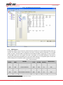
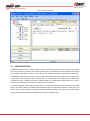
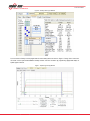
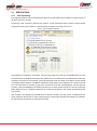
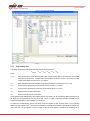
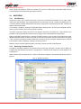
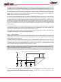
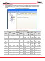
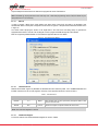
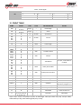
DATA SHEET DM73XX SERIES DIGITAL POWER MANAGER FEATURES APPLICATIONS RoHS compliant for all six substances Compatible with both lead-free and standard reflow processes Programs, controls, and manages up to 32 independent dPOL converters via an industry standard I2C interface (both 100kHz and 400kHz) JTAG IEEE 1149.1 compliant programming interface Controls and monitors industry standard power supplies and other o Telecommunications o Low voltage, high density systems utilizing d-pwerTM Digital Intermediate Bus Architectures Broadband, networking, optical, and wireless communications systems Industrial computing, servers, and o o shift), and feedback loop compensation of the d-pwerTM POL converters User friendly GUI interface for programming, monitoring, and performance simulation Four independent OK lines for flexible fault management and fast fault propagation Four interrupt inputs with programmable hot swap support capabilities Intermediate bus voltage monitoring and protection AC Fail input Non-volatile system configuration data memory 1K Byte of user accessible non-volatile memory Control of industry standard DC-DC front ends Crowbar output to trigger the optional crowbar protection Run-time counter Small footprint semiconductor industry standard QFN64 package: 9x9mm Wide industrial operating temperature range storage applications BENEFITS Eliminates the need for external power management components Communicates with the host system via the industry standard I2C communication bus Reduces board space, system cost, complexity, and time to market peripheral devices (fans, etc) Programs output voltage, protections, optimal voltage positioning, turn-on and turn-off delays and slew rates, switching frequency, interleave (phase DESCRIPTION Power-One’s point-of-load converters are recommended for use with regulated bus converters in an Intermediate Bus Architecture (IBA). The DM73XX is a fully programmable digital power manager that utilizes the industry-standard I2C communication bus interface to control, manage, program and monitor up to 32 dP-series POL converters and 4 independent power devices. The DM73XX completely eliminates the need for external components for power management and programming and monitoring of the d-pwerTM POL converters and other industry standard power and peripheral devices. Parameters of the DM73XX are programmable via the I2C bus and can be changed by a user at any time during product development and deployment. BCD.00317_AA_October-10-2013 1 www.power-one.com/power DATA SHEET 1 SELECTION CHART DPM TYPE NUMBER OF D-PWERTM POLS AND AUXILIARY DEVICES THAT CAN BE CONTROLLED ACTIVE ADDRESSES NUMBER OF GROUPS NUMBER OF INTERRUPTS NUMBER OF PARALLEL BUSES NUMBER OF AUXILIARY DEVICES DM7304G 4 00…03 2 2 2 4 DM7308G 8 00…07 2 2 4 4 DM7316G 16 00…15 3 3 4 4 DM7332G 32 00…31 4 4 8 4 2 ORDERING INFORMATION DM 73 Product family: d-pwer Power Management Devices Series: Digital Power Manager xx Number of d-pwerTM POLs and Auxiliary devices: 04 – 4 devices 08 – 8 devices 16 – 16 devices 32 – 32 devices G – RoHS compliance: G - RoHS compliant for all six substances yyyyy – 5-digit identifier assigned by Power-One for each unique configuration file zz Packaging Option 1): B1 – 50pcs Tube R100 – 100pcs T&R Note: 1 Packaging 2 The option is used only for ordering and not included in the part number printed on the DPM label. evaluation board is available in only one configuration: DM73XX-KIT-HKS Example: DM7316G-12345-R100: A 100-piece reel of 16-node DPMs with preloaded configuration file code 12345. Each DPM is labelled DM7316G-12345. Refer to Figure 1 for label marking information. Figure 1. Label Drawing Line 1: Part Number (7 Char. Alpha Numeric) ZM7316G Line 3: Firmware Rev. (3 Char. Alpha Numeric) A03 DM73xxG xxxxx x xxx xxxxxxx Line 2: Customer Config. Number, Customer Config. Rev. (5 digits Plus Rev Letter) 12345 A Line4: Programming (Location, Date, Batch Code) (7 Char. Alpha Numeric) M082703 3 STANDARD 5-DIGIT IDENTIFIERS DPM TYPE DPM PRELOADED WITH DEFAULT CONFIGURATION FILE DPM CONFIGURED FOR JTAG PROGRAMMING PACKAGING OPTIONS DM7304G 65511 65515 B1, R100 DM7308G 65512 65516 B1, R100 DM7316G 65513 65517 B1, R100 DM7332G 65514 65518 B1, R100 DM73XX Series Digital Power Manager 2 www.power-one.com/power DATA SHEET Reference Documents DP7XXX / DP8XXX Point of Load Regulator Data Sheets DM73XX Digital Power Manager. Programming Manual, Revision A09 or later Graphical User Interface, Revision 6.3.5 or later Programming DM73XX DPMs via JTAG Interface. Application Note ZM00056-KIT USB to I2C Adapter Kit. User Manual 4 ABSOLUTE MAXIMUM RATINGS Stresses beyond those listed may cause permanent damage to the DPM. Exposure to absolute maximum rating conditions for extended periods may affect device reliability. Functional operation of the DPM at absolute maximum ratings or conditions beyond those indicated in the operational sections of this specification is not implied. PARAMETER CONDITIONS/DESCRIPTION MIN MAX UNITS Ambient Temperature Range -40 85 C Storage Temperature (Ts) -55 150 C 125 C Junction Temperature (TJ) 5 Input Voltage VDD pin -0.3 3.6 VDC Input Voltage Any pin other than VDD -0.5 VDD+0.5 VDC Pin Current DC 40 mA MECHANICAL SPECIFICATIONS PARAMETER CONDITIONS/DESCRIPTION Peak Reflow Temperature 40 sec maximum duration MIN Lead Plating Moisture Sensitivity Level 6 7 NOM MAX UNITS 260 C 100% matte tin JEDEC J-STD-020C 3 RELIABILITY SPECIFICATIONS PARAMETER CONDITIONS/DESCRIPTION MIN NOM MAX UNITS Failure Rate Demonstrated at 55C, 60% Confidence Level 2.26 FIT Non-Volatile Memory Endurance -40°C to 85°C ambient 10,000 Read-Write cycles ELECTRICAL SPECIFICATIONS Specifications apply at VDD from 3V to 3.6V, ambient temperature from -40°C to 85°C, and utilizing proper decoupling as shown in Figure 3 unless otherwise noted. BCD.00317_AA_October-10-2013 3 www.power-one.com/power DATA SHEET 7.1 POWER SPECIFICATIONS PARAMETER CONDITIONS/DESCRIPTION MIN Input Supply Voltage VDD pin 3.0 Undervoltage Lockout Hardware reset is triggered below this threshold 2.3 Input Supply Current VDD pin=3.3V VREF voltage AREF pin 2.3 IBVS input voltage range MAX UNITS 3.6 VDC 2.5 2.7 VDC 12 20 mA 2.56 2.7 VDC VREF VDC GND IBVS input resistance 7.2 NOM 100 MΩ FEATURE SPECIFICATIONS PARAMETER CONDITIONS/DESCRIPTION MIN NOM MAX UNITS Intermediate Voltage Bus Protections Overvoltage Protection Threshold With external 5.7:1 ratio divider IBV 14.6 V Undervoltage Protection Threshold With external 5.7:1 ratio divider 0 IBV V Threshold Hysteresis With external 5.7; 1ratio divider. Symmetrical relative to average threshold value Accuracy of Protection Thresholds Internal voltage reference, 1% resistive divider -10 10 %VTH Internal ADC Conversion Error With external 5.7:1 ratio divider -43 43 mV ±114 mV Front End Enable (FE_EN) VFE_EN Front End logic level enabled High VFE_EN Front End logic level disabled Low Isrc Source Current, VFE_EN=VDD-0.5V 5 mA Isink Sink Current, VFE_EN=0.5V 5 mA Crowbar (CB) 7.3 VCB Crowbar Enable High VCB Crowbar Disable Low Isrc Source Current, VCB=VDD-0.5V 5 mA Isink Sink Current, VCB=0.5V 5 mA TCB Duration of Enabling Pulse 1 ms SIGNAL SPECIFICATIONS PARAMETER CONDITIONS/DESCRIPTION SDpu SDthrL SDthrH SDhys SDsink SD pull up resistor SD input low voltage threshold SD input high voltage threshold SD input hysteresis SD sink capability (VSD=0.5V) Clock frequency Sync pulse duration Data=0 pulse duration MIN NOM MAX UNITS 0.52·VDD 0.81·VDD 1.1 30 550 28 78 kΩ V V V mA kHz % of clock cycle % of clock cycle SYNC/DATA Line Freq_sd Tsynq T0 5 0.31·VDD 0.45·VDD 0.37 450 22 72 Interrupt Inputs (INT_N[3:0]) DM73XX Series Digital Power Manager 4 www.power-one.com/power DATA SHEET Rpu3 VthrL3 VthrH3 Vhys3 Pull up resistor Input low voltage threshold Input high voltage threshold Input hysteresis 30 0.31·VDD 0.45·VDD 0.37 0.52·VDD 0.81·VDD 1.1 kΩ V V V 50 0.2·VDD VDD+0.5 kΩ V V 60 kΩ 0.2·VDD VDD+0.5 V V 0.52·VDD 0.81·VDD 1.1 30 kΩ V V V mA ADDR[3:0], ACFAIL_N, RES_N, LCK_N, PG[3:0] Inputs Rpu1 VthrL1 VthrH1 Rpu2 VthrL2 VthrH2 Pull up resistor Input low voltage Input high voltage 20 -0.5 0.7·VDD HRES_N Input HRES_N pull up resistor (with series diode, 30 see note1) HRES_N input low voltage -0.5 HRES_N input high voltage 0.9·VDD Inputs/Outputs (OK_A, OK_B, OK_C, OK_D) OKpu OKthrL OKthrH OKhys OKsink OK pull up resistor OK input low voltage threshold OK input high voltage threshold OK input hysteresis OK sink capability (VOK=0.5V) 5 0.31·VDD 0.45·VDD 0.37 Enable Outputs (EN[3:0]) VEN VEN EN logic level enabled EN logic level disabled EN output high voltage IOH = -10 mA EN output low voltage IOL = 5 mA VENH VENL 7.4 High Low VDD-0.6 V 0.5 V I2C INTERFACE PARAMETER CONDITIONS/DESCRIPTION MIN ViL ViH Vhys VoL tr tof Ii Ci fSCL Input low voltage Input high voltage Input hysteresis Output low voltage, ISINK=3mA Rise time for SDA and SCL Output fall time from ViHmin to ViLmax Input current each I/O pin, 0.1VDD<Vi<0.9VDD Capacitance for each I/O pin SCL clock frequency -0.5 0.7·VDD 0.05·VDD 0 20+0.1Cb2 20+0.1Cb2 -10 0 NOM MAX UNITS 0.3·VDD VDD+0.5 V V V V ns ns μA pF kHz 0.4 300 250 10 10 400 Standard-Mode I2C (fSCL ≤ 100kHz) RPU tHDSTA tLOW tHIGH tSUSTA tHDDAT tSUDAT tSUSTD tSUF External pull-up resistor Hold time (repeated) START condition Low period of the SCL clock High period of the SCL clock Setup time for a repeated START condition Data hold time Data setup time Setup time for STOP condition Bus free time between a STOP and START condition 1 4.0 4.7 4.0 4.7 0 250 4.0 4.7 1000/Cb2 3.45 kΩ μs μs μs μs μs ns μs μs 1 HRES_N Input - Because the input does not have an internal ESD protection diode connected to VDD, the user needs to add an external diode between the HRES_N and VDD pins as shown in Figure 3. 2 Cb – bus capacitance in pF, typically from 10pF to 400pF BCD.00317_AA_October-10-2013 5 www.power-one.com/power DATA SHEET Fast-Mode I2C (100kHz < fSCL≤ 400kHz) RPU tHDSTA tLOW tHIGH tSUSTA tHDDAT tSUDAT tSUSTD tSUF External pull-up resistor Hold time (repeated) START condition Low period of the SCL clock High period of the SCL clock Setup time for a repeated START condition Data hold time Data setup time Setup time for STOP condition Bus free time between a STOP and START condition 1 0.6 1.3 0.6 0.6 0 100 0.6 1.3 300/Cb2 kΩ μs μs μs μs μs ns μs μs 0.9 Figure 2. I2C Timing Parameters t of tHIGH tLOW tr t LOW SCL t SUSTA t HDSTA t HDDAT t SUDAT t SUSTO SDA 8 tBUF TYPICAL APPLICATION Figure 3. Typical Application Schematic of Multiple Output System with Digital Power Manager and I2C Interface Intermediate Voltage Bus IBV Linear Regulator For IBV>3.3V Linear Regulator Crowbar (Optional) Jumper For IBV=3.3V R5 +3.3V C3 6 25 42 57 C4 C5 C6 R6 60 R1 VDD VDD VDD VDD VDD 48 44 R4 SDA SCL R3 C1 R2 IBVS AREF CB FE_EN C2 SD 30 27 45 46 47 36 37 40 41 61 18 16 4 23 17 56 SD SDA SCL OKD OKC OKB OKA ADDR2 ADDR1 ADDR0 INT3_N INT2_N INT1_N INT0_N TDI TDO TCK TMS DM7332 53 20 13 11 34 33 31 32 VIN SD OK VIN OK dPWER POL(s) Group D dPWER POL(s) Group C SD VIN SD OK VIN OK dPWER POL(s) Group B dPWER POL(s) Group A JTAG LCK_N RES_N ACFAIL_N EN3 EN2 EN1 EN0 HRES_N PG3 PG2 PG1 PG0 50 55 7 5 VIN ENABLE VRM 49 51 52 54 POWER GOOD VIN ENABLE LDO ERROR FLAG VSS VSS VSS VSS VSS VSS 8 9 26 38 43 58 The schematic of a typical application of a DM73XX digital power manager (DPM) is shown in Figure 3. The system includes four groups of d-pwer Point Of Load converters (POLs). A group is defined as one or more POL converters interconnected via OK pins. Grouping of the POLs enables users to program advanced fault management schemes and define margining functions, monitoring, start-up behavior, and reporting conventions. DM73XX Series Digital Power Manager 6 www.power-one.com/power DATA SHEET All d-pwer POL converters are connected to the DPM and to each other via a single-wire synchronization/data (SD) line. The line provides synchronization of all POL converters to the master clock generated by the DPM and simultaneously carries bidirectional data transfer between POL converters and the DPM. The DPM communicates via the I2C bus with the host system and/or the Graphical User Interface. In this application, besides POL converters, the DPM also controls and monitors two auxiliary devices – a Voltage Regulation Module (VRM) and a Low Dropout Regulator (LDO). While these devices are not d-pwer compliant and may not even be manufactured by Power-One, they are integrated into the system by communicating with the DPM via their Enable pins connected to ENX outputs of the DPM. In addition, the DPM monitors status of the auxiliary devices via its PGX inputs connected to Power Good and Error Flag outputs of the auxiliary devices. The DPM can control and monitor four or more independent auxiliary devices. The DPM can also trigger an optional crowbar circuit and provide undervoltage and overvoltage protections of the intermediate bus voltage. In addition, the DPM can be controlled by a host system via the interrupt inputs, RES_N and the ACFAIL_N inputs. 9 DESCRIPTION The DM73XX series DPMs perform translation between the I2C interface connected to a host system or the Graphical User Interface and the SD communication bus connected to dPOL converters. In addition, DPMs carry out programming, monitoring, data storage, POL group management, hot-swap control, protection, and control and monitoring of auxiliary devices. The DPMs can be controlled via the GUI or directly via the I2C bus by using specific commands described in the “DPM Programming Manual”. 9.1 DPM MEMORY The DPM memory consists of RAM and non-volatile memory (Flash). The RAM is used for programming operations and manipulation of the various blocks of configuration, setup, status, and monitoring registers. Non-volatile memory is used to store programming and configuration data. Flash memory holds DPM set-up registers, POL set-up registers, monitoring data, and user memory data. Setup registers for the DPM and the POL converters are protected by CRCs that are checked during programming of POL converters and at the power-up of the DPM. The LCK_N pin and the write protection register WP limit the write access to the memory blocks in the DPM and POL converters. The WP register content is defaulted to write protect upon powering up the DPM. 9.1.1 Write Protection There are hardware-based and software-based memory write protections. The hardware protection takes precedence over the software protection. 9.1.1.1 Hardware Protection The LCK_N pin enables the hardware memory write protection. If the pin is pulled low, the hardware lock is active and the memory blocks are then read-only. I2C write commands to the DPM return an error code (0x00). The write commands to the POL converters bypassing the DPM are also disabled. If the pin is left floating, the hardware lock is disabled and the software write protection is active. 9.1.1.2 Software Protection Software write protection allows users to protect the various memory blocks from being overwritten through the I2C bus. At the power-up the WP register is defaulted to write protect. Software write protection can be disabled by checking appropriate boxes in the Write Protection subsection of the DPM/Program/Advanced dialog shown in Figure 4 or via the I2C bus by writing directly into the register. Write protections are automatically restored when the DPM’s input power is recycled. BCD.00317_AA_October-10-2013 7 www.power-one.com/power DATA SHEET Figure 4. GUI DPM Advanced Programming Dialog 9.1.2 DPM Registers The DPM setup registers occupy 70 bytes and contain all necessary information to set up the DPM functionality, define POL converters and Auxiliary Devices, group membership and behavior, margining, interrupt configurations, etc. they DPM registers are listed in. The table relates to the DPM model number DM7332 capable of supporting up to 32 POL converters. For other DPM models some of the registers and/or bits in the registers are not activated depending on the number of supported POLs/Groups/Interrupts/Parallel Buses for the specific DPM. Writing into an unsupported register or bit will have no effect, reading from an unsupported register or bit will return an error code (0x00). Table 1. DPM Setup Registers 3 ADDRESS OFFSET3 REGISTER NAME CONTENT REGISTER TYPE USER ACCESS WRITE PROTECT INITIAL VALUE 0x00 0x04 0x08 0x09 0x0A 0x0B 0x0C 0x0D 0x0E GD1[3:0] GD2[3:0] GAC GBC GCC GDC FPC1 FPC2 EPC Group Definition Register 1 Group Definition Register 2 Group A Configuration Group B Configuration Group C Configuration Group D Configuration Fault Propagation Configuration 1 Fault Propagation Configuration 2 Error Propagation Configuration Static Static Static Static Static Static Static Static Static R/W R/W R/W R/W R/W R/W R/W R/W R/W yes yes yes yes yes yes yes yes yes 0x00000000 0x00000000 0x00 0x00 0x00 0x00 0x00 0x00 0x00 Writing into memory locations beyond address offset 0x96 must be avoided DM73XX Series Digital Power Manager 8 www.power-one.com/power DATA SHEET 0x0F 0x10 0x11 0x13 0x15 0x17 0x1B 0x1F 0x23 0x27 0x28 0x80 0x84 0x88 0x89 0x8B 0x8C 0x8D 0x8E 0x8F 0x91 0x95 0x96 IC1 IC2 IBL[1:0] IBH[1:0] ID[1:0] PB1[3:0] PB2[3:0] PB3[3:0] PB4[3:0] PMC PID[31:0] RTC[3:0] PPS[3:0] EST IBV[1:0] STA STB STC STD REL[1:0] PSS[3:0] DPMS WP Interrupt Configuration 1 Interrupt Configuration 2 IBV Low threshold IBV high threshold DPM Customer Identification Parallel Bus Register 1 Parallel Bus Register 2 Parallel Bus Register 3 Parallel Bus Register 4 Power Manager Configuration POL Identification Register Run Time Counter POL Programming Status Event Status IB Voltage Status of Group A Status of Group B Status of Group C Status of Group D DPM Software Release POL Status Summary DPM Status Write Protection Static Static Static Static Static Static Static Static Static Static Static Run time Run time Run time Run time Run time Run time Run time Run time Static Run time Run time Volatile R/W R/W R/W R/W OTP R/W R/W R/W R/W R/W R/W R R R R R R R R R R R R/W yes yes yes yes N/A yes yes yes yes yes yes Read only 0x00 0x00 0x00 0xFF 0xFFFF 0x00000000 0x00000000 0x00000000 0x00000000 0x00 0x00 value at last shut-down (4x) 0x00 0x00 0x00 0x00 0x00 0x00 0x00 According to DPM type 0x00 0x01 0x00 The static registers are saved in the non-volatile memory and used to store the system configuration data. The run-time registers contain status information and are evaluated during run-time. The Write Protection register WP is a volatile register that defaults to write protect at power-up. 9.1.3 POL Setup Registers Since the POL converters contain only RAM, the data defining performance parameters for each POL and Auxiliary Device, such as the output voltage, protection thresholds, feedback loop compensation, turn-on and turn-off delays, fault management settings, etc., is stored in the POL setup registers in the DPM. The POL setup registers consist of 23 data bytes and 2 CRC bytes. The Auxiliary Device setup registers occupy the same amount of bytes as a POL converter, but only 3 registers have meaningful data. The other registers should be filled with 0x00. The POL setup registers are listed in Table 2. Register significance is different in some cases between the new DP and older ZY series POLs which are still supported. Differences are in bold for the DP series devices. Table 2. POL Setup Registers ADDRESS OFFSET 00h 01h 02h 03h REGISTER+) DP7000/ DP8000 POL PC1_x PC2_x PC3_x TC_x 04h INT_x 05h 06h 07h 08h 09h DON_x DOF_x VLC CLS_x DCL_x 0Ah PC4 0Bh V1H 0Ch V1L 0Dh V2H CONTENT Protection Configuration 1 Protection Configuration 2 Protection Configuration 3 Tracking Configuration Interleave Configuration and Frequency Selection Turn-On Delay Turn-Off Delay Voltage Loop Configuration Current Limit Set-point Duty Cycle Limit Protection Configuration Register 4 Output Voltage Setpoint 1 High Output Voltage Setpoint 1 Low Output Voltage Setpoint 2 High BCD.00317_AA_October-10-2013 ADDRESS OFFSET 00h 01h 02h 03h REGISTER Z7000/ AUX Z8000 POL DEVICE PC1_x EC_x PC2_x reserved PC3_x reserved TC_x reserved 04h INT_x reserved 05h 06h 07h 08h 09h DON_x DOF_x VOS_x CLS_x DCL_x EON_x EOF_x reserved reserved reserved 0Ah B1_x reserved 0Bh B2_x reserved 0Ch B3_x reserved 0Dh C0L_x reserved 9 CONTENT Protection Configuration 1 Protection Configuration 2 Protection Configuration 3 Tracking Configuration Interleave Configuration and Frequency Selection Turn-On Delay Turn-Off Delay Output Voltage Set-point Current Limit Set-point Duty Cycle Limit Dig Controller Denominator z-1 Coefficient Dig Controller Denominator z-2 Coefficient Dig Controller Denominator z-3 Coefficient Dig Controller Numerator z0 Coefficient Low Byte www.power-one.com/power DATA SHEET 0Eh V2L 0Fh V3H 10h V3L 11h CP 12h CI 13h CD Output Voltage Setpoint 2 Low Output Voltage Setpoint 3 High Output Voltage Setpoint 3 Low Controller Proportional Coefficient Controller Integral Coefficient Controller Derivative Coefficient Controller Derivative Roll-Off Coefficient 14h CV 15h 16h 17h 18h 19h 1Ah 1Bh 1Ch 1Dh reserved reserved reserved reserved reserved reserved reserved MRH MRL 1Eh CRC0_x #) 1Fh CRC1_x #) Margining High Selection Margining Low Selection Cyclic Redundancy Check Register 0 Cyclic Redundancy Check Register 1 Dig Controller Numerator z0 Coefficient High Byte Dig Controller Numerator z-1 Coefficient Low Byte Dig Controller Numerator z-1 Coefficient High Byte Dig Controller Numerator z-2 Coefficient Low Byte Dig Controller Numerator z-2 Coefficient High Byte Dig Controller Numerator z-3 Coefficient Low Byte Dig Controller Numerator z-3 Coefficient High Byte 0Eh C0H_x reserved 0Fh C1L_x reserved 10h C1H_x reserved 11h C2L_x reserved 12h C2H_x reserved 13h C3L_x reserved 14h C3H_x reserved 15h 16h 17h 18h 19h 1Ah 1Bh 1Ch 1Dh reserved reserved reserved reserved reserved reserved reserved VOML_x #) VOMH_x #) reserved reserved reserved reserved reserved reserved reserved reserved reserved Output Voltage Margining Low Value Output Voltage Margining High Value 1Eh CRC0_x #) CRC0_x #) Cyclic Redundancy Check Register 0 1Fh CRC1_x #) CRC1_x #) Cyclic Redundancy Check Register 1 Note: +) x denotes the POL address [0..31] #) not downloaded to the POL during programming 9.1.4 Monitoring Data The DPMs can retrieve current, temperature, output voltage, and status information from each of the POL converters and status information only from Auxiliary Devices. Monitoring data is stored in RAM and can be accessed via the I 2C bus. Monitoring registers are read only. The monitoring data consists of 5 Bytes for each POL converter and Auxiliary Device as shown in Table 3. When the status monitoring is enabled, the ST registers get continuously updated. When the parametric monitoring is enabled, the VOH, VOL, IO, and TMP registers get continuously updated. Scaling data from the registers is specific to each DP and ZY series POL. Refer to the DM73XX Programming manual for calculation information. Table 3: Monitoring Data Registers POL CONVERTER 9.1.5 AUXILIARY DEVICE REGISTER CONTENT REGISTER CONTENT ST VOH VOL IO TMP Status Register Output Voltage High Byte Output Voltage Low Byte Output Current Temperature ST reserved reserved reserved reserved Status Register User Memory This non-volatile memory block is reserved for users’ notes and not related to other functions in the DPM. It can be used to save user-specific information such as manufacturing data and location, serial number, application code, configuration file version, warranty or repair information, etc. A total of 1024 Bytes organized in 4 pages is provided. The user memory can be accessed via the GUI System Configuration window shown in Figure 8 or directly via the I2C bus using specific commands. Content of the user memory is saved into the configuration file when the file is saved. Note that this does not change the current DPM contents until the DPM is programmed with the file currently in memory. DM73XX Series Digital Power Manager 10 www.power-one.com/power DATA SHEET Figure 5. User Memory Window 9.2 AUXILIARY DEVICES The DM73XX DPM includes all necessary circuitry to control and monitor four Auxiliary Devices. Virtually any device which has an on/off input and a monitoring output can be an Auxiliary Device. Typical examples of Auxiliary Devices include analog POL converters, linear regulators, and fans. Auxiliary Devices are controlled and monitored via the Graphical User Interface. The DPM treats Auxiliary Devices as d-pwer™ POL converters: each Auxiliary Device has an address and is assigned to one of the groups as shown in Figure 8 (device at addresses 03). Turn-on and off delays can be programmed, and faults can be propagated from POL converters to the devices. Auxiliary Devices are controlled through standard group turn-on and off commands and are fully synchronized with turn-on/off timing of POL converters. Four enable outputs EN0…EN3 control the Auxiliary Devices. Four monitoring inputs PG0…PG3 read status of the Auxiliary Devices. The enable outputs and monitoring inputs are paired together and permanently assigned to specific pins of the DPM as shown in Figure 6. Adding an AUX device is done the same way as adding a POL, select an uncommitted address and then the AUX device desired. In this example two AUX devices are already present. BCD.00317_AA_October-10-2013 11 www.power-one.com/power DATA SHEET Figure 6. Auxiliary Device Type Window Turn-on and turn-off delays can be programmed for each Auxiliary Device as shown in Figure 7. Timing of turn-on and turnoff events can be synchronized between Auxiliary Devices and POL converters by programming appropriate delays for specific types of devices. Figure 7. Sequencing Tracking Window DM73XX Series Digital Power Manager 12 www.power-one.com/power DATA SHEET 9.3 9.3.1 DPM FUNCTIONS POL Programming POL programming is the process of downloading the content of POL setup registers stored in DPM’s non-volatile memory via the SD bus to the POL converters. Programming of POL converters is performed upon power-up, or when the Program button is pressed in the GUI System Configuration window shown in Figure 8, or when the specific command is sent directly via the I2C bus. Figure 8. System Configuration Window The programming is performed in several steps. Once the supply voltage on the VDD pins of the DPM exceeds the UVLO protection threshold, the DPM will start copying setup registers from its non-volatile memory into RAM and execute the cyclic redundancy check (CRC) to ensure integrity of the programming data. When the voltage on the IBVS pin exceeds the IBV undervoltage protection threshold, the DPM will download POL setup registers to the respective POL converter via the SD line. Every data transfer is protected by parity check and followed by the POL acknowledgement and read data back procedure. If both acknowledgement and readback operations are successful, the POL-specific bit in the POL Programming Status registers will be set. The DPM considers the POL converter to be programmed, and continues programming the next POL converter. Upon completion of the programming, the DPM will turn-on the POL converters, if the Auto Turn-On is enabled in the POL Group configuration window shown in Figure 9 (topmost group of square buttons just below "Bus Voltages" tab. Otherwise, the user will need to send the turn-on command via the I2C bus. BCD.00317_AA_October-10-2013 13 www.power-one.com/power DATA SHEET Figure 9. POL Configuration Window 9.3.2 Programming Time Total system programming time can be determined from the following equation: TPROGR TINIT nPOL TPOL n AD TAD Where: TPROGR - time interval from the instant when the DPM supply voltage exceeds DPM’s UVLO threshold until the DPM issues the turn-on command. If the Auto Power-Up is enabled, and the turn-on delay is set to zero, the output voltages start ramping up at the end of TPROGR interval TINIT - DPM initialization interval after the DPM supply voltage exceeds the UVLO threshold. TINIT=11.5ms. TPOL - Time required for programming and verifying of one POL converter. TPOL=26.5ms. TAD - Time required for programming and verifying of one Auxiliary Device. TAD=7.5ms. nPOL - Number of POL converters in the system. nAD - Number of Auxiliary Devices in the system. The programming data (DPM and POL setup registers and the user memory) can be preloaded into DPMs by Power-One or the DPMs can be programmed by the user via the GUI, I2C bus, or JTAG programming interface. The DPMs can be programmed either before or after installation on a host board. To modify POL converter settings, the user can directly access the registers of a POL converter via the I2C bus, bypassing DPM’s POL setup registers. The I2C commands are translated by the DPM and converted into appropriate SD commands to read / write from / into the registers of a POL converter. Writing into these registers is limited by the hardware (LCK_N) DM73XX Series Digital Power Manager 14 www.power-one.com/power DATA SHEET and/or software write protections. Since POL converters do not have non-volatile memory, data written directly into POL converter registers will be lost when the input voltage is removed. 9.4 9.4.1 MONITORING POL Monitoring d-pwerTM and Z-one™ POL converters continuously monitor their own performance parameters such as output voltage, output current, and temperature. The monitored parameters are stored locally in the POL converters and updated every 1ms. If monitoring feature is enabled, the DPM will be continuously copying status and parametric data from POL converters into DPM’s monitoring data registers. The monitoring is enabled by checking the appropriate Retrieve Monitoring bits in the GUI Group Configuration window shown in Figure 9 or directly via the I2C bus by specific commands. If the status monitoring is enabled, the status of each protection (overcurrent, overvoltage, etc.) is being reported. If the parametric monitoring is enabled, then real-time values of voltage, current, and temperature are being reported. Status and parametric monitoring data of a single POL converter and groups of POL converters can be examined in the GUI IBS Monitoring Window shown in Figure 10 or directly via the I2C bus using specific commands. Status data for each group of POL converters is presented in the Group Status block in the left top corner of the window. Parametric data for individual POL converters is shown in Voltage [V], Current [A], and Temp [T] screens. DPMs also monitor and report programming status of each POL converter and results of CRC operations. 9.4.2 Monitoring of Auxiliary Devices The DPM can read status information of the Auxiliary Devices via the PG0…PG3 inputs. The PG0…PG3 are digital 3.3V compliant inputs with internal pull-up resistors. Logic high input on a PGX pin should correspond to normal operation of an Auxiliary Device. Status monitoring data of Auxiliary Devices is stored in the DPM and displayed in the IBS Monitoring Window shown in Figure 10. Figure 10. IBS Monitoring Window BCD.00317_AA_October-10-2013 15 www.power-one.com/power DATA SHEET 9.4.3 Run Time Counter The DPM also monitors the duration of time that it has been in operation. The 4 bytes Run Time Counter is active whenever the DPM is powered up. The count rate is 1 second. The counter is loaded into RAM upon power-up and the new count state is periodically saved to the non-volatile memory. Contents of the counter can be examined in the GUI IBS Monitoring Window shown in Figure 10 or directly via the I2C bus using specific commands. 9.4.4 IBV Monitoring The DPM continuously monitors the intermediate bus voltage via the IBVS input and the built-in 10-bit ADC. The digital representation of the bus voltage is stored in RAM and reported in the IBS Monitoring window shown in Figure 10. In addition, the DPM continuously compares the value of IBV to the Undervoltage and Overvoltage thresholds programmed in the GUI Intermediate Bus Configuration Window shown in Figure 11. Figure 11. Intermediate Bus Configuration Window The thresholds have a symmetric, fixed size hysteresis as shown in Figure 12. Figure 12: Undervoltage (IBL) and Overvoltage (IBH) Protections Hysteresis IBL IBH IBV Low IBV High DM73XX Series Digital Power Manager Hyst Hyst IBV 16 www.power-one.com/power DATA SHEET When the IBV decreases below the IBL threshold minus the hysteresis, the DPM will pull OK lines low turning off all POL converters. The POL converters will execute regular turn-off ramping their output voltages down according to the turn-off delay and falling slew rate settings. In addition, the DPM will clear all bits in the POL Programming Status registers and save the content of the Run Time Counter into the non-volatile memory. The IBV Low bit in the IBS Monitoring Window will change to red. When the IBV recovers above the IBL threshold plus the hysteresis, the DPM will first program all POL converters and then turn them on, if the Auto Turn-On is enabled in the POL Group configuration window shown in Figure 9. Otherwise, the user will need to send the turn-on command via the I2C bus. When the IBV exceeds the IBH threshold plus the hysteresis, the DPM will pull OK lines low turning off all POL converters. The POL converters will execute regular turn-off ramping their output voltages down according to the turn-off delay and falling slew rate settings. In addition, the DPM will save the contents of the Run Time Counter into the non-volatile memory. If the IBV does not decrease below the IBH threshold minus the hysteresis within the next 50ms, the DPM will pull low the FE_EN output and clear all bits in the POL Programming Status registers. The IBV High bit in the IBS Monitoring Window will change to red. If the IBV still does not change, in 50ms the DPM will pull the CB pin high for 1ms to trigger an optional crowbar protection. One second after the IBV decreases below the IBH threshold minus the hysteresis, the DPM will pull the FE_EN high and program all POL converters. Upon completion of the programming process, the DPM will turn on the POL converters, if the Auto Turn-On is enabled in the POL Group configuration window shown in Figure 9. The propagation delay between the IBV increasing/decreasing above/below corresponding thresholds and the DPM pulling down OK lines and triggering the turn-off process is approximately 1ms. 9.4.4.1 Voltage Reference For the purposes of IBV monitoring the user can select either the DPM’s internal voltage reference or an external 2.5V voltage reference. The selection is made by clicking an appropriate radio button in the DPM Configuration/Bus Voltages dialog as shown previously in Figure 11. The DPM’s internal 2.56V voltage reference is effective accuracy of the IBV protection thresholds to 15%. If the accuracy is sufficient, the user does not need to make any changes to the schematic shown in Figure 3. If higher accuracy of the IBV monitoring is desired, then a 2.5V external reference can be added as shown in Figure 13. The GUI automatically changes values of the IBL and IBH thresholds when the reference selection is changed. Note: If the Reference Voltage setting is changed during operation of the DPM, then the power to the DPM needs to be cycled or the HRES_N pin needs to be pulled low and released. Figure 13. External Voltage Reference Connections IBV 47k R1 VDD VDD IBVS 10n AREF 10k U1 C1 U1 and R1 are additional components. U1 is an industry standard 2.5V voltage reference such as TL431 or similar. C1 is an existing component but its value changes depending on the type of voltage reference. Common voltage reference part numbers and values of associated components are shown in Table 4. BCD.00317_AA_October-10-2013 17 www.power-one.com/power DATA SHEET Table 4. Component Values For External Reference U1 Part Number TL431 ZR431 Manufacturer TI Zetex Accuracy, % 0.5, 1, 2 0.5, 1, 2 R1, Ohms 100-620 510-2000 C1, μF ≥ 10 ≥ 0.01 Accuracy of the protection thresholds in the case of external reference is determined by the sum of accuracy of the voltage reference, accuracy of the 10k/47k resistive divider shown in Figure 13, and conversion error of the internal ADC specified in 7.2. 9.5 POL GROUP MANAGEMENT POL converters and Auxiliary Devices can be arranged in up to four groups. A group of POL converters is defined as a number of POL converters with interconnected OK pins. Auxiliary Devices are added to a group in the GUI, without any external connections. A group can include from 1 to 32 POL converters, but a POL converter can be a member of only one group. In addition, the OK lines can be connected to the DPM to facilitate propagation of faults and errors between groups. One DPM can manage up to four independent groups: A, B, C, and D, depending on model of the DPM. Group management includes fault and error propagation, margining, turn-on and turn-off, monitoring setup, and interrupt configuration. 9.5.1 Fault and Error Propagation dP-series POL converters protect outputs by triggering either a fault or an error depending on the severity of the problem (see POL converter datasheets). Fault propagation between POL converters belonging to the same group is a programmable function of POL converters. The DPM allows propagating faults and errors between groups of POL converters and, in case of an error, to a DC/DC front-end and an optional crowbar. The propagation delay for fault/error propagations is less than 10μs. To enable fault and error propagation, the respective bits needs to be checked in the GUI Fault and Error Propagation window shown in Figure 14. Note that cross propagation of faults/errors (means fault in Group X propagates to Y and vice versa) should be avoided. Figure 14. Fault and Error Propagation Window. DM73XX Series Digital Power Manager 18 www.power-one.com/power DATA SHEET The fault propagation from POL converters to the auxiliary devices can be disabled by checking the bit in the Auxiliary Device Fault Management window as shown in Figure 15. It is not possible to propagate a fault from an Auxiliary Device to POL converters. Figure 15. Auxiliary Device Fault Management Window Table 5. Fault and Error Propagation Scenarios Protection Triggered Propagation Between POLs Propagation To Auxiliary Devices in the Same Group as the Faulty POL UVP or OTP Enabled Disabled Any Disabled UVP or OTP Enabled Enabled Any Disabled UVP or OTP Enabled Enabled Disabled Enabled UVP or OTP Enabled Enabled Enabled Enabled Enabled Disabled Any Disabled Fast turn-off Enabled Enabled Any Disabled Fast turn-off Enabled Enabled Disabled Enabled Fast turn-off Enabled Enabled Enabled Enabled Fast turn-off OVP or Phase Voltage Enabled Disabled Any Disabled OVP or Phase Voltage Enabled Enabled Any Disabled OVP or Phase Voltage Enabled Enabled Disabled Enabled OVP or Phase Voltage Enabled Enabled Enabled Enabled Tracking or OCP Tracking or OCP Tracking or OCP Tracking or OCP BCD.00317_AA_October-10-2013 Propagation To Auxiliary Devices in Other Groups Propagation Between Groups of POLs Faulty POL Regular turn-off Regular turn-off Regular turn-off Regular turn-off Fast turn-off, low side FET is ON Fast turn-off, low side FET is ON Fast turn-off, low side FET is ON Fast turn-off, low side FET is ON 19 POLs in the Same Group as the Faulty POL Auxiliary Devices in the Same Group as the Faulty POL POLs in Other Groups Auxiliary Devices in Other Groups Regular turn-off Regular turn-off Regular turn-off Regular turn-off Regular turn-off Regular turn-off Regular turn-off Regular turn-off Continue operating Turn-off with turn-off delay Turn-off with turn-off delay Turn-off with turn-off delay Continue operating Turn-off with turn-off delay Turn-off with turn-off delay Turn-off with turn-off delay Continue operating Continue operating Regular turn-off Regular turn-off Continue operating Continue operating Regular turn-off Regular turn-off Continue operating Continue operating Continue operating Turn-off with turn-off delay Continue operating Continue operating Continue operating Turn-off with turn-off delay Fast turnoff Continue operating Continue operating Continue operating Continue operating Continue operating Regular turn-off Continue operating Regular turn-off Turn-off with turn-off delay Fast turnoff Fast turnoff Fast turnoff Turn-off without turnoff delay Turn-off without turnoff delay Turn-off without turnoff delay www.power-one.com/power DATA SHEET When propagation is enabled, the faulty POL converter pulls its OK pin low. A low OK line initiates turn-off of other POL converters in the group and signals the DPM to pull other OK lines low to initiate turn-off of other POL converters as programmed. The regular turn-off of a POL converter means that the output voltage is ramping down according to its turn-off delay and falling slew rate settings. If a POL converter triggers an undervoltage or overtemperature fault, it will initiate the regular turnoff. In the case of an overcurrent or tracking fault, the POL converter initiates the fast turn-off by opening both high and low side switches instantaneously. If either output overvoltage or phase voltage errors are triggered, the faulty POL converter initiates the fast turn-off and turns on its low side switch. In addition, when an error is propagated, the DPM can generate commands to turn off a front end (a DC-DC converter generating the intermediate bus voltage) and trigger an optional crowbar protection to accelerate removal of the intermediate bus voltage (IBV). Once the fault has recovered in the faulty POL converter, the other POL converters will turn on in a controlled manner according to their turn-on delay and rising slew rate settings. 9.5.2 Margining Margining can be executed separately for each group by clicking an appropriate radio button in the GUI IBS monitoring window shown in Figure 10 or directly via the I2C bus by the margining command. All POL converters in a group are margined in the same direction (up or down) by the percentage programmed individually for each POL converter. 9.5.3 Turn-ON and Turn-Off Automatic turn–on upon application of the input voltage is enabled by checking the Auto Turn-On bit in the GUI Group Configuration window shown in Figure 9. Turn-on and turn-off of various groups during the operation is controlled from the GUI IBS Monitoring window or directly via the I2C bus by specific commands. 9.5.4 Interrupt Configurations The DPM has four interrupt inputs that can be programmed to: Inhibit the operation of one or several Groups of POL converters when pulled low or Act as a Group Reprogramming Trigger. The two functions are mutually exclusive – an interrupt can be either programmed as an Inhibit or as a Group Reprogramming Trigger. The interrupts are programmed in the GUI Interrupt Configuration window shown in Figure 16 or directly via the I2C bus by specific commands. In Figure 16 the Interrupt 0 is programmed as the inhibit for group A and the Interrupt 2 is programmed as the group C reprogramming trigger. 9.5.4.1 Group Inhibit An interrupt input can be programmed to act as an inhibit on a single or multiple groups of POL converters. When the interrupt input is pulled low, the DPM will pull the appropriate OK lines low. The affected POL converters will execute regular turn-off ramping their output voltages down according to the turn-off delay and falling slew rate settings. Once the interrupt is released, the POL converters will automatically turn-on according to their turn-on delay and rising slew rates settings. The inhibit function can be used for a variety of applications, such as Hardware-based control of groups of POL converters and Auxiliary Devices Delayed turn-on at power-up (Automatic Turn-On is enabled but the interrupts are held low during powerup. Note that POL converters can be programmed even when an interrupt is held low.) The interrupt inputs should be controlled with open collector devices. The propagation delay between the external device pulling the interrupt input low and the DPM pulling down OK lines and triggering the turn-off process is approximately 10μs. This option is set as part of DPM/Configure/Faults dialogs. DM73XX Series Digital Power Manager 20 www.power-one.com/power DATA SHEET Figure 16. Interrupt Configuration Dialog 9.5.4.2 Group Reprogramming Trigger An interrupt that is programmed as a group reprogramming trigger always acts only on one group of POL converters. Interrupt 0 acts on Group A, Interrupt 1 acts on Group B and so on. The assignment is fixed and cannot be changed by the user. When the interrupt is pulled low, the DPM will program the group of POL converters. Upon completion of the programming, the DPM will turn-on the POL converters, if the Auto Turn-On is enabled. When the interrupt input is released, the DPM will pull the appropriate OK line low. The POL converters in the group will execute regular turn-off ramping their output voltages down according to the turn-off delay and falling slew rate settings. In addition, the DPM will clear all bits in the POL Programming Status registers. The group reprogramming trigger is mostly used to support hot swap of boards and daughter cards that do not have a DPM installed on them as shown in Figure 17. Figure 17: INT0 Configured as Group A Reprogramming Trigger Mother Board or Back Plane Group A Daughter Card IBV GND SD POL POL POL DM7300 Vox SD OK_ A INT0 _N In this configuration the Interrupt 0 (INT0_N) is configured as the group A reprogramming trigger. The DPM is installed on a mother board or a backplane. A daughter card with a group of POL converters is being inserted in the system during normal operation. At first, the long pins carrying power and the OK_A line signal make contact. Then the short pins carrying the SD and interrupt signals make contact. Once the interrupt senses low input voltage, it will command the DPM to program all POL converters in the group A. Upon completion of the programming, the DPM will turn-on the POL converters, if the Auto TurnOn is enabled. When the daughter card is being removed, the interrupt input is released as soon as the short pins break the contact. The DPM will immediately pull the OK_A line low turning off all POL converters in the group A according to the turn-off delay and falling slew rate settings. BCD.00317_AA_October-10-2013 21 www.power-one.com/power DATA SHEET 9.6 9.6.1 CONTROLS ACFAIL_N and RES_N The ACFAIL_N and RES_N are active low digital inputs. When one of the inputs is pulled low, the DPM will pull all OK lines low turning off all the POL converters and the Auxiliary Devices in all groups. The POL converters will execute regular turnoff ramping their output voltages down according to the turn-off delay and falling slew rate settings. In addition, the DPM will clear all bits in the POL Programming Status Registers and save the contents of the Run Time Counter into the non-volatile memory. The AC_FAIL in or RES_N in bit in the IBS Monitoring Window will change to red. When the input is released, the DPM will first program all POL converters and then turn them on, if the Auto Turn-On is enabled. Otherwise, the user will need to send the turn-on command via the I2C bus. The ACFAIL_N is typically connected to an AC-DC front end. Whenever the AC voltage disappears, the ACFAIL_N signal will be set low. If there is no battery backup, it usually means the DC output will disappear after 20ms. If the turn-off delays and falling slew rates of each POL converter are set to the values such that all POL converters will have fully turned off within the hold time of the AC-DC front end, then output voltage tracking during turn-off is guaranteed. The RES_N input has the same functionality as the ACFAIL_N input and can be connected to a simple turn on/off switch or to a sensor that shuts the entire system down when it is activated. The ACFAIL_N and RES_N inputs should be controlled with open collector devices. The propagation delay between the external device pulling the input low and the DPM pulling down OK lines and triggering the turn-off process is approximately 1ms. 9.6.2 Front End Enable The FE_EN pin is dedicated to the control of a DC-DC Front End. The Front End is typically used to convert the 48V into the intermediate bus voltage (IBV). If the DPM is powered from an auxiliary source, not from the IBV, it can control the DC-DC Front End. When FE_EN is internally pulled up to 3.3V, the Front End is enabled. The FE_EN output can provide up to 5mA of current. When the FE_EN goes low, the Front End is disabled. The Front End can be enabled and disabled via the GUI IBS Monitoring Window or directly via the I2C bus using specific commands. The FE_EN pin should not be directly connected to the Enable pin of the DC-DC Front End. Typically, the Enable pin is referenced to the primary side of the Front End that is isolated from the low voltage secondary side. In addition, the Enable pin can be pulled up internally to a voltage potentially damaging to the DPM FE_EN output. The best method is to interface the DPM with the Front End through an optocoupler as shown in Figure 18. This configuration provides interface for negative logic front ends. Figure 18. Interface Between DPM and DC-DC Front End Front End DPM FE_EN R 3.3k Enable Q -VIN GND 9.6.3 Crowbar When the crowbar protection is enabled, the CB pin is internally pulled up to 3.3V for 1ms. It is capable of supplying 5mA to turn on a crowbar circuit. DM73XX Series Digital Power Manager 22 www.power-one.com/power DATA SHEET 9.6.4 HRES_N The HRES_N is an active low digital input. When it is pulled low, the DPM will perform full hardware reset including processor, memory, and communication interface. The POL converters and auxiliary devices will be turned off although sequencing and tracking during the turn-off are not guaranteed. Communication with a host processor or GUI (if established) will be lost. When the input is released, the DPM will first program all POL converters and then turn them on, if the Auto Turn-On is enabled. Unlike all other I/O pins on the DM73XX DPM, the HRES_N does not have an internal ESD protection diode connected to VDD. Therefore, it is necessary to add the diode externally as shown in Figure 3. The HRES_N function is intended as an emergency reset and except as indicated below, should not be used in normal system operation. It is necessary to use an external reset circuit (see Fig. 3) to hold the HRES_N line low until the VDD supply reaches steady state conditions. Power-One Inc. successfully tested the On-Semi voltage detector p/n NCP303LSN27T1 although other similar devices can also be utilized. Alternatively, the HW_RES pin can be connected to the output of a CPLD (or similar device) and controlled via the system supervisory circuitry. 9.7 COMMUNICATION INTERFACES 9.7.1 I2C Interface The DM73XX series DPMs have the industry standard I2C interface fully meeting the requirements of the I2C -Bus Specification Version 2.1 from Philips Semiconductors. The I2C interface is working in the following configurations: standard (100kbs) and fast (400kbs) data transfer rates 7-bit addressing: 4 MSBs fixed, 3 LSBs programmable by ADDR [2:0]. The address prefix of the DM73XX is 0x50. This allows encoding DPM addresses 0x50, 0x52, …, 0x5E (Bit0 is the read/write bit) The DPM always acts as the I2C slave while the host processor always acts as the I2C master. Refer to the “DPM Programming Manual” for the detailed description of the I2C communications. Note: It is recommended to use Power-One’s ZM00056-KIT USB to I2C Adapter kit for the communication between a DPM and a computer with the Power-One I2CGraphical User Interface. 9.7.1.1 Watchdog Timer In order to prevent occasional hanging of the I2C bus, a watchdog timer is started whenever an I2C command is initiated. If the command is not executed before the watchdog times out, the DPM will assume that the I2C bus is in an error condition (e.g. the SCL or SDA lines are pulled low continuously) and it will reset the I2C bus. The watchdog timeout is 1000ms. Since the watchdog function is not a part of the standard I2C specifications, it can be disabled by the user. 9.7.2 JTAG Interface The DM73XX series DPMs feature the JTAG interface that can be used for programming the DPM with user-specific configuration settings. JTAG boundary-scan capabilities are not currently supported. JTAG-programmable DPMs have unique 5-digit identifiers listed in Table 6. Table 6. JTAG Programmable DPM Part Numbers BASE PART NUMBER 5- DIGIT IDENTIFIER DM7304G 65515 DM7308G 65516 DM7316G 65517 DM7332G 65518 BCD.00317_AA_October-10-2013 23 www.power-one.com/power DATA SHEET Only the DPM part numbers listed in the table can be programmed via the JTAG interface. Note: The DPMs can be programmed via the JTAG only once. After initial programming via the JTAG, the DPMs may be reprogrammed via I2C as necessary. 9.7.2.1 SVF File In order to program a DPM via the JTAG interface, the Serial Vector Format (SVF) file needs to be generated. Click Generate SVF button in the System Configuration window shown in Figure 8. It will open the SVF Generator window shown in Figure 19. The window allows specifying the location of the target DPM in the JTAG chain and setting delays to generate the appropriate Serial Vector Format file. The resulting file is used to program the DPMs through the JTAG interface. Refer to “Programming DM73XX DPMs via JTAG Interface” Application Note for more details. Figure 19. SVF File Generator Window 9.7.2.2 JTAG Instructions DM73XX series DPMs support only BYPASS and IDCODE instructions defined by IEEE 1149.1. SAMPLE/PRELOAD and EXTEST instructions are not currently supported. Summary of the supported instructions is shown in Table 7. Table 7. JTAG Instructions INSTRUCTION OPCODE REGISTER FUNCTION BYPASS 1111 Bypass Places the 1-bit bypass register between the TDI and TDO pins, which allows the BST data to pass synchronously through the DPM to other devices in the JTAG chain IDCODE 0001 JTAG ID Selects the ID register and places it between the TDI and TDO Note: The Instruction Register is 4-bit wide 9.7.2.3 Identification Register Format and contents of the JTAG Identification Register are shown in Table 8. DM73XX Series Digital Power Manager 24 www.power-one.com/power DATA SHEET Table 8. JTAG ID Register MSB BIT LSB 31 28 27 12 11 1 0 DESCRIPTION Version Part Number Manufacturer’s Identity 1 CONTENTS 0000 1001010100000010 00000011111 1 10 PINOUT TABLE PIN NAME VDD VSS PIN NO. 6, 25, 42, 57, 60 8, 9, 26 38, 43, 58 PIN TYPE BUFFER TYPE PIN DESCRIPTION Supply --- Positive Supply Supply --- Ground SD 56 I/O ST/OCPU Sync-Data Line OKA OKB OKC OKD 11 13 20 53 I/O ST/OCPU OK Lines FE_EN 17 O CMOS Front-End Enable CB 23 O CMOS Crowbar Trigger SDA 30 I/O ST/OC I2C Interface SCL 27 I/O ST/OC I2C Interface ADDR0 ADDR1 ADDR2 IN0_N IN1_N IN2_N IN3_N TCK TMS TDO TDI EN0 EN1 EN2 EN3 PG0 PG1 PG2 PG3 47 46 45 41 40 37 36 31 32 33 34 5 7 55 50 54 52 51 49 I STPU I2C Interface Address I STPU Interrupts RES_N JTAG Interface O CMOS Auxiliary Device Enables I STPU Auxiliary Device Power Good 18 I STPU System Soft Reset ACFAIL_N 16 I STPU AC-Fail Trigger LCK_N 61 I STPU Write Protect Lock HRES_N 4 I STPU Cold Reset IBVS 48 I A Intermediate Bus Voltage Sense AREF 44 - A Analog Reference IR 63 nc 1, 2, 3, 10, 12, 14, 15, 19, 21, 22, 24, 28, 29, 35, 39, 59, 62, 64 - - NOTES Leave open, if JTAG interface is not utilized See important usage instructions in paragraph 10.6.4 Internal Reset Connect to VSS via 10k No Connect Leave floating Legend: I=input, O=output, I/O=input/output, P=power, ST=Schmitt-trigger, OCPU=open collector with pull-up, OC=open collector, CMOS=CMOS output stage, STPU=Schmitt-trigger with pull-up, A=analog BCD.00317_AA_October-10-2013 25 www.power-one.com/power DATA SHEET 11 PINS DESCRIPTION ACFAIL_N, AC Fail Input (Pin 16): Schmitt-Trigger input with internal pull-up resistor (active low). Pulling low the input indicates to the DPM that an AC-DC front-end has lost the mains and that a system shut down should immediately be initiated. ADDR[0:2], I2C Address Inputs (Pins 47, 46, 45): Inputs with internal pull-up resistor. The 3 bit encoded address determines the DPM communication address for the I2C interface. AREF, Analog Reference (Pin 44): An analog reference which is used internally. A 10nF capacitor should be connected as close as possible to the package between AREF and VSS. See 9.4.4.1. CB, Crowbar Output (Pin 23): A CMOS output which is used to trigger a crowbar (SCR) in case of overvoltage on the Intermediate Voltage Bus. EN[0:3], Enable Outputs for Auxiliary Devices (Pins 5, 7, 55, 50): CMOS outputs to control Auxiliary Devices like linear regulators, analog POLs, fans or other devices. .FE_EN, Front-End Enable (Pin 17): A CMOS output which is used to turn-on/off the DC/DC converter generating the IBV. HRES_N, Hardware Reset (Pin 4): Input with internal pull-up resistor. When pulled low a cold start of the Digital Power Manager is initiated. Refer to paragraph 10.6.4 for important information regarding connections of this pin. IBVS, Intermediate Voltage Bus Sense (Pin 48): Analog input to an internal ADC circuit to measure the Intermediate Bus Voltage. The full scale range of the input is 2.56V and the IBV should be scaled down by a factor of 5.7 for proper reporting of the IBV with the d-pwer™ GUI. INT[0:3], Interrupts (Pins 41, 40, 37, 36): Four active low inputs with internal pull-ups. Each of the inputs can be configured for two functions: first, the interrupt input acts on the OK line(s) to stop momentarily the operation of group of POLs and Auxiliary Devices, second the interrupt can be used as a hot swap trigger. In this function the interrupt input triggers the programming of a group. When released, POLs are assumed to be disconnected from the DPM. IR, Internal Reset (Pin 63): Connect to VSS via a 10kOhm resistor. LCK_N, Memory Lock (Pin 61): Active low input with internal pull-up. When LCK_N is pulled low, all memory within the DPM is write-protected. The write protection cannot be disabled by software. OKA, OKB, OKC, OKD, Group OK Signals (Pins 11, 13, 20, 53): An open drain input/output with internal pull-up resistor. Pulling low the OK input will indicate to the DPM a fault in a Group, the DPM can also pull an OK line low to disable a Group. PG[0:3], Power Good (Pins 54, 52, 51, 49): Input with internal pull-up resistor. The pin is used to read the status of an Auxiliary Device. RES_N, Active Low Reset In/Out (Pin 18): Input with internal pull-up resistor. When pulled low a soft reset of the system (sequenced turned off of all POLs and Auxiliary Devices) is initiated. When released the whole system is reprogrammed and started if necessary. SD, Sync Data Line (Pin 56): An open drain input / output with internal pull-up resistor. Communication line to distribute a master clock to all converters and at the same time to communicate with all POLs. JTAG Interface (Pins 34, 33, 32, 31): Connect to a JTAG IEEE-1149.1-compliant programmer supporting SVF files or leave open, if not used. VDD, Positive Supply (Pins 6, 25, 42, 57, 60): Supply voltage. At least 4x100nF decoupling capacitors should be connected between VDD and VSS pins. All VDD pins must be connected. VSS, Ground (Pins 8, 9, 26, 38, 43, 58): Ground. Decoupling capacitors need to be connected as close as possible to the pins. All VSS pins must be connected. NC, No Connect (Pin 1, 2, 3, 10, 12, 14, 15, 19, 21, 22, 24, 28, 29, 35, 39, 59, 62, 64): All nc pins must remain floating. DM73XX Series Digital Power Manager 26 www.power-one.com/power DATA SHEET 12 MECHANICAL DRAWINGS Figure 20. DM73XX Mechanical Drawing Figure 21. DM73XX Terminals BCD.00317_AA_October-10-2013 27 www.power-one.com/power DATA SHEET mm A J A1 D/E D1/E1 D2/E2 N P e L b inch MIN NOM MAX MIN NOM MAX 0.80 0.0 0.01 0.20 ref 9.00 BSC 8.75 BSC 4.70 1.00 0.05 0.032 0.000 - 0.040 0.002 4.50 4.90 0.008 ref 0.354 BSC 0.344 BSC 0.185 0.177 0.193 64 0.24 0.42 0.50 BSC 0.40 0.25 0.30 0.18 0.60 0.009 0.55 0.30 0.012 0.007 0.016 0.020 BSC 0.016 0.010 0.024 0.022 0.012 Notes: 1. Compliant to JEDEC standard MO-220 variation VMMD-3 64 nc PG3 EN3 PG2 PG1 OKD PG0 EN2 SD VDD VSS nc VDD LCK_N nc IR nc Figure 21. DM73XX Mechanical Drawing – Top View 49 1 48 IBVS nc ADDR0 nc ADDR1 HRES_N ADDR2 EN0 AREF VDD VSS EN1 VDD VSS INT0_N EXPOSED PAD CONNECT TO VSS VSS INT1_N nc nc OKA VSS nc INT2_N OKB INT3_N nc nc nc TDI 16 33 TCK SDA nc nc SCL VSS VDD nc nc CB nc OKC nc FE_EN 32 RES_N 17 TDO TMS ACFAIL_N JTAG Note: - all "nc" - pins must remain floating - all "VSS" - pins need to be connected together - all "VDD" - pins need to be connected together Note: I2C is a trademark of Philips Corporation. NUCLEAR AND MEDICAL APPLICATIONS - Power-One products are not designed, intended for use in, or authorized for use as critical components in life support systems, equipment used in hazardous environments, or nuclear control systems without the express written consent of the respective divisional president of Power-One, Inc. TECHNICAL REVISIONS - The appearance of products may change depending on the date manufactured. Specifications are subject to change without notice. DM73XX Series Digital Power Manager 28 www.power-one.com/power Mouser Electronics Authorized Distributor Click to View Pricing, Inventory, Delivery & Lifecycle Information: Power-One: DM7332G-B1 DM7316G-B1 DM7304G-B1 DM7308G-B1 DM7332G-65514-B1 DM7304G-65511-R100 DM7316G65513-B1 DM7308G-65512-R100 DM7316G-65513-R100 DM7308G-65512-B1 DM7304G-65511-B1 DM7332G65514-R100