1
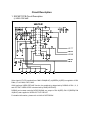
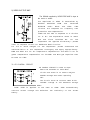
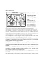
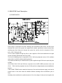
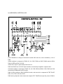
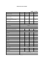
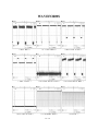
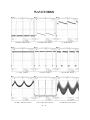
SERVICE MANUAL
BUYER
:
REV
: “B”
MODEL NAME : KT-1948
DATE
: JANUARY, 2003
KORTEK CORPORATION
CONTENTS
1. PRECAUTIONS
******
2
2. SOCKET PCB CIRCUIT DESCRIPTION ******
3. MAIN PCB
4. PART LIST
******
******
5. SPECIFICATION
******
6. TIMMINIG CHART
******
7. WAVE FORMS
8. TROUBLE SHOOTING GUIDE
9. BLOCK DIAGRAM
5
9
16
******
23
24
25
******
******
27
28
10. MAIN PCB TOP MARKING
******
29
11. SOCKET PCB TOP MARKING
******
30
12. SCHMATICS
******
31
KORTEK Corporation
KT-1948
1.PRECAUTIONS
1-1 SAFETY PRECAUTIONS
WARNINGS : Service should not be attempted by anyone unfamiliar with the necessary
precautions on this monitor. The following precautions are necessary during servicing.
1) For continued safety, do not attempt to modify the circuit board.
2) Disconnect the AC Power before servicing.
3) When the Monitor is operating, do not touch any heatsink on the Chassis as it is self-heated.
FIRE & SHOCK HARZARD
1) During servicing, pay attention to the original wires whether it is uncoated or undressed,
especially the wires in the high voltage circuit section. If there is any uncoated or melted wire is
found, then please do not try to replace the related parts, and wait for the qualified service person's
coming.
2) Many electrical, mechanical parts in this monitor have special safety-related characteristics for
protection against shock hazard and others. These characteristics are often passed unnoticed by a
visual inspection and the protection afforded by them cannot necessarily be obtained by using
replacement component rated for higher voltage wattage,etd
Replacement parts which have these special characteristics are identified in the manual and
supplements by shading on the schematic diagram and the parts list.
3) When replacing Chassis, always be certain that all the protective devices are installed properly.
4) leakage current check(figurel 1)
KORTEK Corporation
KT-1948
READING SHOULD
NOT BE ABOVE 0.45mA
DEVICE
UNDER
TEST ALL
TEST
LEAKAGE CURRENT
EXPOSED METAL
TESTER
SURFACES
2-WIRE
CORD
ALSO TEST WITH PLUG
REVERSED(USING AC
EARTH
ADAPTER PLUG AS
GROUND
REQUIRED)
Figurel 1
(TEST METHODE)
1-1-2. X-RADIATION
WARNING : The only potential source of x-radiation is the picture tube, however when the
high voltage. Circuitry is operating properly, there is no possibility of an xradiation problem.
factory
The basic precaution is to keep the high voltage at the
recommended level.
1) To measure the high voltage, use a high-impedance high-voltage meter.
Connect(-) to chassis and (+) to the CRT anode cap.
2) Turn the contrast control max. clockwise.
3) Measure the high voltage. The high voltage meter should indicate the following factory
recommended level
4) If the actual level exceeds the max. factory set level, then immediate service is required to
prevent the possibility of premature failure of components
5) To prevent X-RADIATION possibility, it is essential to use the specified picture tube.
6) The nominal high voltage is 24KV and not exceed 27KV at zero beam current at rated voltage.
32 - 3
KORTEK Corporation
KT-1948
1-2. SERVICING PRECAUTION
WARNING 1 : First, reading "safety precaution" section of this manual. If unforeseen
circumstances create conflict between the servicing precautions and safety
precaution, always follow the safety precautions.
WARNING 2 : A high voltage VR replaced in the wrong direction may cause excessive
X-RAY Emitting.
WARNING 3 : An electrolytic capacitor installed which the wrong polarity might explode.
1) Servicing precautions are printed on the label, and should be followed closely.
2) Always unplug the AC power cord from the AC power source before attempting to remove
or reinstall any component or assembly,disconnect PCB plugs or connectors,connect all test
Components in parallel which an electrolytic capacitor.
3) After servicing, always check that the screw,components and wiring have been correctly
reinstalled. Make sure that the area around the serviced part has not been demaged.
4) Check the insulation between the blades of the AC plug and accessible conductive
parts(example : metal parts, input terminals)
5) Never touch any of the locked B+ voltage. Do not apply AC power to the unit(or any of its
Assemblies) unless all solid-state heatsinks are correctly installed.
6) Always connect a test instrument's ground lead to the instrument chassis ground before
connecting the positive lead; always remove the instrument's ground lead last.
Circuit Description
1. SOCKET PCB Circuit Description
1) VIDEO PRE AMP
Video signal (0.7V PP) supplied from CN901 PIN2(BLUE), 4(GREEN), 6(RED) is supplied to IC901
PIN4, 6, 8 via C902, C903, C905.
IC901 performs VIDEO PRE AMP function, the amplitude is determined by DCBIAS of PIN 1, 2, 3,
and OUT PUT VIDEO LEVEL is determined by PIN9(CONTRAST).
DCBIAS and contrast controlled VIDEO SIGNAL are output to PIN 19(RED) PIN 17(GREEN) PIN
13(BLUE) and supplied to VIDEO OUT PUT CIRCUIT.
For detailed information, please refer to KA2141 DATE BOOK.
2) VIDEO OUT PUT AMP
The SIGNAL supplied by VIDEO PRE AMP is input to
the base of Q903.
The
amplitude
EMITTER
of
Q903
RESISTOR
RESISTOR
R937,
circuits
are
is
R938
R945,
composed
determined
and
and
for
by
COLLECTOR
L903,
C935
frequency
loss
prevention and compensation.
VIDEO OUT PUT AMP is composed of 3 circuits
(R. G. B), the explanation above is about
RED
and
since
LOCATION
NO.
for
the
components are applied differently, please
refer to complete circuit for GREEN and BLUE circuits.
For A/S or value changes for the components, please understand the
characteristics of the components thoroughly and apply appropriately.
R938 and R937 are for 1%( temperature compensation) and R945 is for 5%
grade (temperature compensation for TR Q903) and NPO type capacitor must
be used for C935.
3) G2 CONTROL CIRCUIT
G2 CONTROL CIRCUIT is used to omplement the movement of AUTO BIAS
circuit and there is no need to adjust
SCREEN voltage even when replacing
CRT.
The circuit works as follows. When R.G.B
CATHODE voltage of CRT detected through
R936,
R931,
controls
evenly.
R933
screen
is
applied
voltage
to
and
the
base
maintains
of
the
Q904,
Q904
luminosity
automatically
of
the
screen
4)AUTO BIAS CIRCUIT
AUTO BIAS CIRCUIT is the
circuit which detects the
space between the cathod
of CRT and GRID 1 and
automatically adjusts BIAS
voltage.
It compensates the color
changes when warming up
and maintains evenly.
Further, it extends the lifetime by compensating the
emission loss when CRT is
used for long time and CRT can be replaced without additional adjustment when A/S.
The description of circuits is as follows. PIN4 of SUB PCB is connected with the cathode of CRT.
CRT CATHODE is composed of 3 electrodes (R, G, B) and GRID1 is also composed of 3
electrodes. The electrodes maintain spaces different from each other and BIAS voltage should
supply voltages proportional to these spaces to acquire even color. Since the principle of the circuit
operation is identical for R, G and B, RED circuit will be described as an example.
CRT CATHODE emits hot electrons when the voltage is supplied to the heater of CRT and the
temperature of the surface of adjacent CRT cathode reaches 900
and over.
Then the hot electron moves toward CRT FACE though there are some differences according to
the conditions of voltage applied to GRID1, GRID2, GRID3,5, and the current is produced toward
opposite way, which shows up at CRT RED cathode.
SUB PCB PIN4 is connected with RED cathode, passes through R962 and the changes in current
and voltage occurs at the emitter of Q953.
This changed current is displayed in the waveform and is sent to IC950 to amplify since it is very
poor signal.
IC950 amplifies in R956, R957, R955 ratio and sends the signal to PIN3 of IC950 for secondary
amplification. The secondary amplification of IC950 is performed in
R952, R964 ratio and the
pulse is transformed into DC LEVEL by ZD950 and C952.
Transformed DC voltage controls Q951, Q952, Q950 and is sent to SUB PCB PIN6 to control the
base of Q953.
When the base voltage of Q953 changes, the voltage of emitter changes and controls the amount
of hot electrons of CRT cathode.
The operation forms FEED BACK LOOP and maintains fixed value through
repetition.
5) PULSE GENERATOR
PULSE GENERATOR CIRCUIT supplies power to the control of AUTO BIAS circuit
and produces and supplies pulse only while blanking period to prevent error.
For more detailed TIMING CHART, please refer to the waveform of the circuit
diagram.
The description of the circuit is as follows. HORIZONTAL & VERTICAL BLANK PULSE is supplied
through R917, adjusts the waveform delay and width to ease AUTO BIAS movement at PULSE
OSCILLATOR circuit composed of IC902, C920, R921, R923, R924, R922 and output to PIN 7 of
IC902.
Since the output waveform can not have enough current the waveform is output to PIN1 after
amplifying the current using OP AMP and supplies the current to AUTO BIAS CONTROL CIRCUIT.
2. MAIN PCB Circuit Description
1) POWER SUPPLY
Power supply is composed of line filter, switching amp and switching trans circuit, line filter circuit
eliminates the noise of the power line supplied from outside, prevents the noise occurred from
switching amp from flowing out through outer power line, and the circuit is composed of C101,
L101, C102, C103 and C104.
The AC power supplied through line filter is then supplied to D101 and transformed into ripple
current and finally transformed into DC by C105.
The circuit of switching amp is composed of IC101, Q101 and peripheral circuits, IC101 oscillates
and controls, and Q101 performs switching function.
IC101 starts oscillation by the transformed DC power supplies through R102 and outputs the pulse
to PIN6.
IC101 PIN3, R106, R115 and R108 are composed to form OVER LODE prevention circuit, and
IC101
PIN1,2 and the peripheral circuits of IC102 performs voltage adjustment and stabilization
function.
T102 is SYNC TRANS used to match the frequency of the monitor and power supply, and used to
prevent noise on the screen when the distance between switching trans and deflection yoke is
close.
Switching trans transforms the produced pulse to fit to the voltage of each part and supplies the
pulse to these parts, DC voltage is supplied to PIN2 of T101, the pulse is produced at PIN4, and
PIN6,7 is composed of a circuit which feeds back the changed amount of voltage and supplies
VCC of IC101.
PIN15 is a circuit supplying horizontal deflected voltage through +49V LINE, and is composed of
D120, C120, L110 and C121.
R120 and C131 are improved FCC and SMOKE NOISE circuits.
PIN9 of T101 is the circuit supplying voltage to VIDEO OUT PUT AMP through +110V line and the
circuit is composed of D121, C123, L111 and C124.
PIN10 is the circuit supplying +B to VERTICAL OUT PUT AMP with +40V line and is composed of
D122 and C125.
PIN11 is the circuit supplying activation voltage to HORIZONTAL & VERTICAL OSC IC with +12V
line and is composed of D123, C126, L112, C127 and C132.
PIN12 is supplying voltage to CRT heater through +6.3V line and the circuit is composed of
D124,C128, L113, R116 and C129. As other circuits for power supply, auto and manual degaussing
circuits are composed of PH101 and RL101.
2) HORIZONTAL & VERTICAL MODE CONTROL CIRCUIT
IC601 is in charge of horizontal & vertical sync and mode control, checks H.V SYNC input through
PIN3,4 then output through PIN5,6, and regardless of input SYNC output SYNC is always output in
negative value.
PIN1,2 forms oscillator circuit of IC601, and is composed of C601, C602, X601 and R603
PIN15 ~ PIN23 output low signal from corresponding mode after checking the status of input H.V
SYNC.
Here, the output low signal and inverted high signal from Q603 control horizontal position,
horizontal size, vertical size, pincushion, etc.
PIN24 uses +5V for the activation voltage of IC601, and ZD603 and R607 are in charge of this
function.
AR601 performs pull-up resistor function for I PIN15 ~ PIN22 of C601 and supplies +5V to each
gate.
3) CONTROL CIRCUIT
+40V is supplied to PIN1
of control circuit, and
the voltage is transformed into +5V by R814,
D801 and C801.
+5V is controlled by VBLN, S-PIN, V-SIZE,
V-POSI, H-SIZE, H-POSI
and VR, output to PIN5,
,7,8,11,12 of CN801, adjusted by H-SIZE, H-POSI and VR, output to PIN5,6,7,8,11,12 of CN801
and controls IC301.
SW801 functions as manual degaussing switch and the output is to PIN9 of CN801 via R817.
VR801 is contrast control VR and outputs the voltage controlled into PIN2 of CN801.
VR810 is sub contrast VR, adjusts MAX value, and VR809 controls MIN value..
4) HORIZONTAL DRIVE CIRCUIT
Horizontal drive pulse is applied to the
gate of Q402 via C407 and D406 and
R407 form BIAS circuit.
+12V is supplied to T402 and PIN7 of
T402 generates pulse from switching
Q402.The generated pulse is exposed
to PIN4,1 of T402 and is supplied to
horizontal output TR.
R401 is resistor for current regulation
and C417 performs noise filter function.
C406 is the circuit for input current restraint and noise elimination.
5) HORIZONTAL & VERTICAL OSC
IC301 TDA4858 is in charge of horizontal & vertical OSC and drive, and is activated by +12V of
PIN9.
Vertical oscillator is composed of PIN22, 23, 24, C306, R306 and C305, PIN28 controls V-BLN,
PIN18 V-SIZE and PIN17 V-POSI.
Vertical drive output is performed by PIN12 and 13.
PIN14 and PIN15 are V.H SYNC input terminals, and are always supplied in negative value.
Horizontal oscillator is composed of PIN27, 28, 29, C302, R303 and R304. C303, R305 and C304
connected to PIN26 perform AFC function.
PIN2 of IC301 performs X-RAY CONTROL function, and the circuit is composed of F.B.T PULSE,
D301, C311, R313, R312 and C307.
PIN5 and its peripheral circuits detect and compare F.B.T PULSE and output the pulse to PIN6 for
constant high voltage at anytime.
VR301 is high voltage control VR and since its high voltage is adjusted to 24.5KV at the
manufacturing process, there is no need to adjust when performing A/S.
PIN11 of IC301 and its peripheral circuits control H-SIZE. The voltage proportional to the changing
value of DC voltage and high voltage of PIN32 is output to PIN11 and controls Q408 and Q410 to
control H-SIZE.
Moreover, S-PIN and V-BLN are composed at PIN11 and is adjusted by Q408 and Q410.
6) HORIZONTAL OUT PUT CIRCUIT
HORIZONTAL OUT PUT CIRCUIT is composed of OUT PUT TR Q401, FLY BACK
TRANSFORMER T401, Q403 and VR401, Q411, Q412 which are RASTER POSITION ADJUST
CIRCUIT.
T501 and its peripheral circuits connected to PIN14 of T401 are forming DYNAMIC FOCUS circuit.
HORIZONTAL DRIVE PULSE is supplied to the base of Q401, and pulse is generated at resonant
circuit which is composed of T401, HORIZONTAL DEFLECTION YOKE, C401 and C402.
PIN2 of T401 is supplied with controlled voltage from Q403. The voltage is supplied in varied
values depending on the frequency. It is as follows. 31.5KHz
54V,
38KHz
65V,
48KHz
85V.
Pulse of 800 ~ 900V value is generated at PIN1 of T401 and the high voltage is supplied to the
anode of CRT after boosting the value to 24.5KV.
Moreover, T401 supplies FOCUS, SCREEN voltage to CRT.
VR401 is horizontal raster position control VR, and is supplied +10V from T401 PIN3, -10V PIN4
respectively, and change DC voltage to Q411 and Q412 to move the horizontal raster to the left or
right..
7) VERTICAL OUT PUT CIRCUIT
IC302 TDA4866 is VERTICAL OUT
OUTPUT CIRCUIT. It is the circuit
Which generates sawtooth wave
form needed for deflection and
supply to deflection yoke.
The waveform supplied to DRIVE
1, 2 is boosted and output to PIN6.
12V is supplied to PIN3 of IC302
and +40V is supplied to PIN7.
R334 and R335 are 1%(F grade) FEED
BACK resistors used for
circuit
accuracy and temperature compensation.
SPECIFICATIONS
MODEL : KT-1948
PARAMETER
OPERATING VOLTAGE
MIN
TYP
MAX
UNITS
100
115/230
230
VAC
85
90
WATTS
< 0.40
0.45
mA
< 2.0
2.4
mA
OPERATING POWER
LEAKAGE CURRENT TO CHASSIS GND.
AT 250VAC, 50/60HZ
(LINE/NEUT, IN COMMON)
HI-POT LINE/NEUT, IN COMMON TO
SECONDARY/CHASSIS 1500VAC 50/60HZ,
NO BREAKDOWN
OPERATING TEMPERATURE
10
60
DEGREES C
REL. HUMIDITY OPERATING
10
90
%
IMPLOSION PROTECTION
PROVIDEO BY BAND AND MOUNTING LUGS
MAGNETIC SHIELD
INTERNAL
DEGAUSSING
MANUAL / AUTO
VIDEO SIGNAL
+ 0.7Vpp, 75 OHM-MONITOR TERMINATIONS
RASTER DIM, ADJUST RANGE VERTICAL
< 235
> 330
mm
RASTER DIM, ADJUST RANGE HORIZONTAL
< 323
> 395
mm
640 £ª 480 / 1024 £ª 768 / 800 £ª 600
MODE
PINCUSHION
MIS-CONVERGENCE
3.0
%
CENTER
0.25
0.3
mm
CORNERS
0.35
0.45
mm
100
HZ
¡¾5
HZ
VERTICAL
SCAN RATE
45
HOLD IN RANGE
HIGH LEVEL
3.0
5.0
5.5
VOLT
LOW LEVEL
0.0
0.0
1
VOLT
5
%
50
KHZ
¡¾500
HZ
NON-LINEARITY
HORIZONTAL
SCAN FREQ
31
HOLD IN RANGE
SYNC.
PLARITY
POSITIVE
HIGH LEVEL
3.0
5.0
5.5
VOLT
LOW LEVEL
0.0
0.0
1
VOLT
5
%
NON-LINEARITY
X= 281 ¡¾ 0.020
WHITE BALANCE
LUMINANCE
y= 311 ¡¾ 0.020
ADJUSTABLE WITH USER CONTROL 10 ¡¾ 3(F/L) ~ 55 ¡¾ 5(F/L)
29 - 20
TIMMING CHART
MODEL : KT- 19 4 8
IGT
IBM
31.5k/60
PREQUNCY
§Ô
VESA
31.5K/60
31.5/50§Ô
§Ô
35k/56§Ô
38K/60§Ô
48K/60§Ô
RESOLUTION
640*480
640*480
640*480
800*600
800*600
1024*768
DOT FREQ
25.175M§Ô
25.175M§Ô
25.175M§Ô
36.000M§Ô
40.000M§Ô
65.000M§Ô
H PREQ
31.469K§Ô
31.469K§Ô
31.469K§Ô
35.156K§Ô
37.879K§Ô
48.363K§Ô
H DISPLAY
25.422US
25.422US
25.422US
22.222US
20.000US
15.754US
H BP
1.907US
1.907US
1.907US
3.556US
2.200US
2.462US
H SW
3.813US
3.813US
3.813US
2.000US
3.200US
2.092US
H POL
POSITIVE
POSITIVE
NEGATIVE
POSITIVE
POSITIVE
NRGATIVE
V PREQ
59.940
50.00
59.940
56.250§Ô
60.317§Ô
60.004§Ô
V DISPLAY
15.253mS
15.253mS
15.253mS
17.067mS
15.840mS
15.880mS
V BP
1.048mS
1.048mS
1.048mS
0.626mS
0.607mS
0.600mS
V SW
0.064mS
0.064mS
0.064mS
0.057mS
0.106mS
0.124mS
V POL
POSITIVE
POSITIVE
NEGATIVE
POSITIVE
POSITIVE
NEGATIVE
INTERACE
NON
NON
NON
NON
NON
NON
29 - 21
WAVEFORMS
B
A
( VID EO INPUT )
D
C
( H . C LAM P SIG NAL )
F
E
( VID EO O UTPU T )
G
( AUTO BIAS +B PULSE )
( VID EO D RIVE O UTPU T )
( AUTO BIAS PULSE O UTPU T )
H
( AUTO BIAS PULSE INPUT )
I
( H .V BLANKING INPUT )
29 - 22
( G 1 PULSE )
WAVEFORMS
J
L
K
( H .D EFLEC TIO N PULSE )
( V.D EFLEC TIO N PULSE )
N
M
( V SYN C O UTPU T )
( V D RIVE PULSE )
O
( +B C O NTRO L PULSE )
( H SYN C O UTPU T )
P
Q
( H .SIZE C O NTRO L PULSE )
( F.B.T FEED BAC K PULSE )
R
29 - 23
( D YNAM IC FO C US PULSE)