1
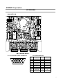
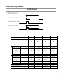
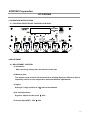
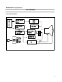
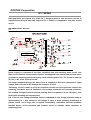
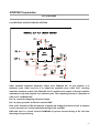
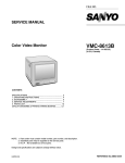
COLOR CRT MONITOR
SERVICE
DOC. NO
KT-XX03NA-SM
DATE
2004 .02. 02
REV. NO
0
REV. DATE
-
MANUAL
KT-1903NA / KT-1703NA
KT-1403NA
KORTEK CORPORATION
CONTENTS
1.PRECAUTIONS
******
3
2.PRODUCT SPECIFICATIONS
******
6
3.OPERATING INSTRUCTIONS
******
10
4.ADJUSTMENT
******
10
5.BLOCK DIAGRAM
******
12
6.GENERAL THEORY OF OPERATION
******
13
7.TROUBLE SHOOTING GUIDE
******
26
8.WAVE FORM
******
33
9.BILL OF MATERIAL
******
36
10.SCHEMATICS
******
51
2
KORTEK Corporation
KT-XX03NA
1.PRECAUTIONS
1-1 SAFETY PRECAUTIONS
WARNINGS : Service should not be attempted by anyone unfamiliar with the necessary
precautions on this monitor. The following precautions are necessary during
servicing.
1) For continued safety, do not attempt to modify the circuit board.
2) Disconnect the AC Power before servicing.
3) When the Monitor is operating, do not touch any heatsink on the Chassis as it is self-heated.
1-1-1 FIRE & SHOCK HARZARD
1) During servicing, pay attention to the original wires whether it is uncoated or undressed,
especially the wires in the high voltage circuit section. If there is any uncoated or melted
wire is found, then please do not try to replace the related parts, and wait for the qualified
service person's coming.
2) Many electrical, mechanical parts in this monitor have special safety-related characteristics for
protection against shock hazard and others. These characteristics are often passed unnoticed
by a visual inspection and the protection afforded by them cannot necessarily be obtained
by using
replacement components rated for higher voltage wattage,etc.
Replacement parts which have these special characteristics are identified in the manual and
supplements by shading on the schematic diagram and the parts list.
3) When replacing Chassis, always be certain that all the protective devices are installed
properly.
4) leakage current check (figure 1)
3
KORTEK Corporation
KT-XX03NA
READING SHOULD
NOT BE ABOVE 0.45mA
DEVICE
UNDER
TEST ALL
TEST
EXPOSED METAL
LEAKAGE CURRENT
TESTER
SURFACES
2-WIRE
CORD
ALSO TEST WITH PLUG
REVERSED(USING AC
EARTH
ADAPTER PLUG AS
GROUND
REQUIRED)
Figurel 1
(TEST METHODE)
1-1-2. X-RADIATION
WARNING : The only potential source of x-radiation is the picture tube, however
when the high voltage. Circuitry is operating properly, there is no possibility
of an x-radiation problem.
at the factory
The basic precaution is to keep the high voltage
recommended level.
1) To measure the high voltage, use a high-impedance high-voltage meter.
Connect(-) to chassis and (+) to the CRT anode cap.
2) Turn the contrast control max. clockwise.
3) Measure the high voltage. The high voltage meter should indicate the following factory
recommended level
4) If the actual level exceeds the max. factory set level, then immediate service is required to
prevent the possibility of premature failure of components
5) To prevent X-RADIATION possibility, it is essential to use the specified picture tube.
6) The nominal high voltage is 24KV and not exceed 27KV at zero beam current at rated voltage.
4
KORTEK Corporation
KT-XX03NA
1-2. SERVICING PRECAUTION
WARNING 1 : First, reading "safety precaution" section of this manual. If unforeseen
circumstances create conflict between the servicing precautions and safety
precaution, always follow the safety precautions.
WARNING 2 : A high voltage VR replaced in the wrong direction may cause excessive
X-RAY Emitting.
WARNING 3 : An electrolytic capacitor installed which the wrong polarity might explode.
1) Servicing precautions are printed on the label, and should be followed closely.
2) Always unplug the AC power cord from the AC power source before attempting to remove
or reinstall any component or assembly, disconnect PCB plugs or connectors, connect all test
Components in parallel which an electrolytic capacitor.
3) After servicing, always check that the screw, components and wiring have been correctly
reinstalled. Make sure that the area around the serviced part has not been demaged.
4) Check the insulation between the blades of the AC plug and accessible conductive
parts(example : metal parts, input terminals)
5) Never touch any of the locked B+ voltage. Do not apply AC power to the unit(or any of its
Assemblies) unless all solid-state heatsinks are correctly installed.
6) Always connect a test instrument's ground lead to the instrument chassis ground before
connecting the positive lead; always remove the instrument's ground lead last.
5
KORTEK Corporation
KT-XX03NA
2.Product Specifications
2-1 SPECIFICATION
PARAMETER
MIN
TYP
MAX
UNITS
100
115/230
230
VAC
OPERATING POWER
85
90
WATTS
LEAKAGE CURRENT TO CHASSIS GND
< 0.40
0.45
mA
< 2.0
2.4
mA
OPERATING VOLTAGE
AT250VAC,50/60Hz(LINE/NATU,IN COMMON)
HI-POT LINE/NEUT, IN COMMON
OPERATING TEMPERATURE
10
60
DEGREE
REL,HUMIDITY OPERATING
10
90
%
MAGNETIC SHIELD
INTERNAL
DEGAUSSING
MANUAL TYPE
VIDEO SIGNAL
+0.7Vpp, 75 Ohm MONITOR TERMINATIONS
RASTER DIM ADJUST RANGE VERTICAL
< 190
> 290
mm
RASTER DIM ADJUST RANGE HORIZONTAL
< 300
> 350
mm
MODE
640*480
PINCUSHION(ALL BRIGHTNESS)
3.0
%
MIS-CONVERGENCE CENTER
0.25
0.3
mm
MIS-CONVERGENCE CORNERS
0.35
0.45
mm
VERTICAL
SCAN RATE
60/70
±5
Hz
5.0
5.0
VOLTAGE
0.0
0.6
VOLTAGE
5
%
31.6
Khz
±500
Hz
HOLD IN RANG
SYNC +5V
74LS LEVELS
LOW
0.0
Hz
NON-LINEARITY
HORIZONTAL
SCAN FREQUENCY
31.2
31.4
HOLD IN RANG
SYNC POLARITY
POSITIVE
SYNC +5V
5.0
5.0
5.0
VOLTAGE
0.0
0.0
0.6
VOLTAGE
5
%
74LS LEVELS
LOW
NON-LINEARITY
WHITE BALANCE & LUMINANCE
X=
281 ±20 y=
311 ±20
Y = 10 ±3 F/L
Y = 56 ±5 F/L
6
KORTEK Corporation
KT-XX03NA
2-2 PCB DIMENSIONS
1) MAIN PCB
7
KOREK Corporation
KT-XX03NA
2)SOCKET PCB
2-2-1 15-PIN SIGNAL CABLE CONNECTOR
1
6
11
2-2-2 PIN DESCRIPTION
P_NO
PIN_NAME
P_NO
PIN_NAME
1
RED VIDEO
9
NC
2
GREEN VIDEO
10
SHIELD GND
3
BLUE VIDEO
11
SHIELD GND
4
NC
12
NC
5
NC
13
H-SYNC
6
RED GND
14
V-SYNC
7
GREEN GND
15
NC
8
BLUE GND
8
KORTEK Corporation
KT-XX03NA
2-3 TIMING CHART
A
HORIZONTAL VIDEO
BC
D
HORIZONTAL SYNC
F
VERTICAL VIDEO
VERTICAL SYNC
NO
1
2
3
4
MODE
IGT
IBM VGA
IBM VGA
IBM VGA
H
640
640
720
640
V
480
350
400
480
H
POSI
POSI
NEGA
NEGA
V
POSI
NEGA
POSI
NEGA
FREQUENCY
㎑
31.469
31.469
31.469
31.469
PERIOD
㎲
31.777
31.777
31.777
31.777
SYNC
㎲
3.813
3.813
3.813
3.813
B/P
㎲
1.907
1.094
1.907
1.907
ACTIVE
㎲
25.422
25.422
25.422
25.422
FREQUENCY
㎐
59.941
70.087
70.087
59.941
PERIOD
㎳
16.683
14.268
14.268
16.683
SYNC
㎳
0.064
0.064
0.064
0.064
F/P
㎳
1.049
1.907
1.080
1.049
ACTIVE
㎳
15.253
11.122
12.711
15.253
FIXEL FREQUENCY
㎒
25.175
25.175
28.322
25.175
NO
NO
NO
NO
RESOLUTION
SYNC POLARITY
H
V
INTERACE
9
KORTEK Corporation
KT-XX03NA
3. OPERATING INSTRUCTIONS
3-1 LOCATION FUNCTION OF CONTROL PCB ASS'Y
4.ADJUSTMENT
4-1 ADJUSTMENT CONTROL
1) Orientation
When servicing, always face the monitor to the east
2) Warm-up time
The monitor must be on for 30 minutes before starting alignment. Warm-up time is
especially critical in color temperature and white balance adjustments.
3) Signal
Analog 0.714vpp positive at 75Ω, internal termination.
4) B+ line adjustment
Signal in; adjust in order to 54 ± 0.2V
5) Screen adjust(FBT) : 550 ± 20V
10
KORTEK Corporation
KT-XX03NA
4-2 DISPLAY CONTROL ADJUSTMENTS
A. SELECT
H-SIZE
FUNCTION,
ADJUST
TO
THE
HORIZONTAL
SIZE
IS
SIZE
IS
350mm±3mm(V/R404)
B. SELECT
V-SIZE
FUNCTION,
ADJUST
TO
THE
VERTICAL
250mm±3mm(V/R304)
C. SELECT H-POSI FUNCTION, ADJUST TO CENTER THE PATTERN WITHIN THE
RASTER (V/R305)
D. SELECT V-POSI FUNCTION, ADJUST TO CENTER THE PATTERN WITHIN THE
RASTER(V/R501)
E. SELECT S-PCC FUNCTION, ADJUST SIDE PINCUSHION ON THE EDGE.(V/R405)
F. Remove H-SYNC to make H–SYNC flow and vary V/R301 to adjust frequency at 31.5
±0.2 Khz.
G. Remove V-SYNC to make V-SYNC flow and vary V/R302 to adjust vertical frequency
at 56 ±0.5Hz.
Adjust other specific lines at 47 ±0.5Hz.(adjust it differently according to the
request of buyer.)
H. ADJUSTMENT FOCUS1 VR & FOCUS2 VR ON FBT TO THE OPTIMUM.
11
KORTEK Corporation
KT-XX03NA
5. BLOCK DIAGRAM
R
G
B
VIDEO PRE-AMP
VIDEO
KA2141
DRIVE
H
V
SIGNAL CONTROL
AUTO BIAS
74LS86
H/V PROCESS
TDA9102C
54V
POWER
SUPPLY
VERTICALOUT
TDA8172
S-CORRECTION
125V
12V
6.3V
26V
FBT
SCREEN
FOCUS
H,V
12
KORTEK Corporation
KT-XX03NA
6. GENERAL THEORY OF OPERATION
6-1 BLOCK DIAGRAM
Above is the block diagram of the monitor as a whole. Each major section is
presented in a block. The individual circuit that makes up the section is covered later and is
not shown here. This simple block diagram will allow you a fundamental understanding of
the complete monitor. This will help when covering the sections individually. The process
from video signal to video display starts with the video signal generated from the source.
The signal is composed of information that is fed into various sections of the monitor
the following diagrams are based on 17"/19” VGA auto bias monitor and are included for
reference only. Actual circuit may be different. Please see update schematic and parts list
enclosed.
6-2 VIDEO DRIVE SECTION
13
KORTEK Corporation
KT-XX03NA
Video signal (0.7V PP) supplied from "CN901 Pin 2 (BLUE), 4(GREEN), 6(RED)" is supplied
to IC901 Pin 4, 6, 8 through "C902, C903, C905." IC901 performs VIDEO PRE AMP and its
amplitude is “determined by DC BIAS of Pin 1, 2, 3. Pin 9 (Contrast) controls its output
video level.
Video signal passing through the DCBIAS and the Contrast Control is output to Pin 19(RED),
Pin 17 (GREEN), Pin 13(BLUE) and supplied to video output circuit.
For details, see KA2141 Date Book.
6-3 VIDEO OUT PUT AMP SECTION
Signal supplied from video PRE AMP is sent to Q903 base. The amplitude of Q903 is
determined by emitter resistor R938 and collector resistor R937 and R945. Circuit of L903
and C935 are configured for prevention from and compensation of loss of high frequency.
Video output amp is composed of three circuits of R. G and B. The above description is about RED
circuit. For description of GREEN and BLUE circuit, see the entire circuit because LOCATION
Numbers of the parts are differently applied. In A/S or when changing values of the parts, apply them
with full understanding of parts’ characteristics. R938 and R937 are 1% (for temperature
compensation) and R945 is 5% (temperature compensation for TR Q903), and for C935, make sure to
use a capacitor of NPO type.
14
KORTEK Corporation
KT-XX03NA
6-4 G2 CONTROL CIRCUIT SECTION
G2 control circuit complements operations of auto bias circuit and when replacing CRT, it is
not necessary to adjust screen voltage. For circuit operations, R. G. B cathode voltage of
CRT is detected through R936, R931 and R933. When the voltage is applied to Q904 base,
Q904 automatically controls screen voltage to maintain screen brightness at a constant
level.
6-5 AUTO BIAS CIRCUIT SECTION
Auto bias circuit automatically controls BIAS voltage by detecting the separation between
cathode of CRT and grid 1, and compensates for color changes in warm-up to maintain
them constantly. Also, when using CRT for a long period, the circuit lengthens life of CRT
by compensating for deterioration of emission and helps to replace CRT without any other
adjustment in A/S. SUB PCB Pin 4 is connected to cathode of CRT.
15
KORTEK Corporation
KT-XX03NA
CRT cathode is composed of three electrodes of R, G and B and GRID 1 electrode is also
composed of three electrodes. Three electrodes maintain different separations from each
other and the voltage proportional to each separation should be supplied to obtain the
constant color. Because operational principle of circuit is same for R, G and B, RED circuit
will be described instead of describing all circuits. When heater voltage is supplied to CRT
and surface temperature of the nearest CRT cathode exceeds 900℃, CRT cathode emits
heat electrons. At this time, despite of that there are a few differences due to the conditions
of voltage supplied to GRID 1, GRID 2 and GRID 3 and 5, heat electrons generally move to
CRT face and current is generates to the opposite direction. The current appears on the
surface of CRT RED cathode. SUB PCB Pin 4 is connected to RED cathode and current and
voltage passing through R962 change in Q953 emitter. This changed current appears in the
form of wave signal on Q953 collector, and sent to IC950 to be amplified. IC950 amplifies the
signal at rate of R956, R957 and R955 and sends it to IC950 Pin 3 for the second
amplification. Second amplification of IC950 is made at rate of R952 and R964 and pulse is
converted to DC level by ZD950 and C952. The converted DC voltage is sent to SUB PCB
Pin 6 by controlling Q951, Q952 and Q950 and controls Q953 base. When the voltage of
Q953 base changes, emitter voltage changes and controls emission of heat electrons from
CRT cathode. This operation is made through feedback loop and maintains a constant value
with repeat.
6-6. PULSE GENERATOR CIRCUIT
Pulse generator circuit supplies control power to auto bias circuit. The circuit makes and
supplies pulse in order for auto bias circuit to operate only during blanking period for
preventing error. For detailed timing chart, see waveform of Circuit Diagram.
The circuit is supplied horizontal & vertical blank pulse through R917, and controls the
delay and the width of the waveform for easy operation of auto bias at the pulse oscillator
circuit, which is composed of IC902, C920, R921, R923,
16
KORTEK Corporation
KT-1903NA
R924 and R922, and outputs it to IC902 Pin 7. Output waveform, with not much current, is
amplified with using OP amp and output to Pin 1. Finally it is supplied to auto bias control
circuit.
6-7 SMPS CIRCUIT SECTION
Power supply is composed of line filter, switching amp and switching trans circuit. Line
filter circuit removes noise element of power line supplied from outside and prevents noise
generated in switching amp from flowing out to external power line. The circuit is made up
of C101, L101, C102, C103 and C104."
AC voltage supplied through line filter circuit is supplied to D101 and converted to ripple
voltage, and converted to DC through the operation of C105.
"Switching circuit is made up of IC101 peripheral circuits and IC101 performs control and
switching operations such as oscillation, over-voltage protection and overload protection.
DC rectified through D102 and lowered passing R102 is supplied to IC101 3Pin(Vcc), then
IC101 start operating and outputs pulse.
NO. 3 Pin has over-voltage shutdown function embedded in chip. if high (operates stably at
approximately 23 ~ 35V) voltage or low voltage is input, it stops operating temporarily to
protect circuit, and if high load is applied momentarily, embedded overload shutdown
function blocks circuit operation and protects circuit to maintain stable operation in
outputting pulse.
17
KORTEK Corporation
KT-XX03NA
IC101 pin 1 has OSC function embedded in chip so that, at the first time when power switch
is turned on, embedded OSC oscillates to drive circuits. After the initial operation, it inputs
pulse separated flowing out from FBT in IC101 Pin 5 to match frequencies of monitor and
power supply so that it minimizes noise from oscillation and from interference between
frequencies of monitor and power supply. Also, when distance between trans and deflection
yoke is near, it prevents noise from being generated on screen.
The switching trans changes and supplies the generated pulse adequately for voltage of
each part of monitor, and IC101 Pin 4 receives feedback for difference in voltages output to
terminal receiving feedback for variations of voltage, and increases voltage when it is low,
and lowers when it is low, so supplying the secondary voltage stably.
T101 secondary side receives the output of the pulse provided to the primary side. T101 pin
9 rectifies the voltage at the D116, smoothes it at C116 and outputs 125 V and provides it to
the video output terminal. R117 and C117 are the circuits to improve the FCC and smoke
noises.
"T101 Pin 9 is made up of +125V D116, C116, J175 and R116 circuit."
"Pin 10 and Pin 14 are GNG on the secondary voltage. "Pin 11 supplies voltage to CRT
heater in +6.3V line and its circuit is composed of D111, C123 and R123.
Pin 12 supplies operating voltage of video pre amp, horizontal & vertical OSC IC in +12V line,
and its circuit is composed of D112, C126 and R126.
With regard to R111, IC102, Q101, R110, C115, R112, VR101 and R114, in order to supply
voltage to the second side stably, the voltage provided to IC102 through R111 oscillates the
light emission element and generates the potential and feeds back it to IC101 pin4. Then, it
maintains and controls a stable voltage of the secondary side. Also, they can control B+
voltage using Q101 V/R101, so controlling desired voltage.
Pin 13 is a circuit supplying B+ of vertical output amp and horizontal drive in +26V line and
its circuit is composed of D110 and C119, BD104 and C122.
Pin 15 supplies B+ voltage of FBT in 54V line and its circuit is composed of D109, C118,
D114 and C121. Pin 16 is output for compensating for voltage according to frequency
changes and its circuit is composed of D108, BD101, C124, D118, R118 and Q102. Because,
with horizontal frequency, B+ of FBT varies with Q102 operation, this is a circuit for
compensating for this.
Other circuits of power supply constitute manual degaussing circuit with PH101.
18
KORTEK Corporation
KT-XX03NA
This is a circuit using temperature characteristics of PH101, and when power is turned on,
high voltage is applied momentarily and current flows. At this time, heat is generated and
temperature rises. With rising temperature, as much as resistance increases and after about
20 seconds, current stops flowing and this circuit stops operating.
6-8 Horizontal/Vertical Processor Section
IC301 (TDA9102C) oscillates with embedded OSC, outputs vertical and horizontal frequency
in free running, and even though SYNC is not supplied from outside, it can operate.
IC301 supplies 12V voltage to Pin 20 to drive it.
With Pin 1 and Pin 2, in free running, horizontal oscillation frequency is determined and
with R313 and C309, free running frequency is determined.
Pin 3 compares and matches SYNC phase input from outside and phase of embedded OSC,
and it performs mainly with R315, C307, C308, R314 and R312, and adjusts DC level with
VR301.
Pin 4, input terminal of horizontal SYNC, is compatible with TTL and always triggers
negative.
19
KORTEK Corporation
KT-XX03NA
Pin 5 supplies sync input from outside to Pin 5 through embedded interface and at this time,
according to capacitor value of C305 connected to Pin 5, pulse width is determined.
Pin 6 outputs horizontal output pulse and its range is from 27Khz to 70Khz.
Pin 7.20 is used as terminal supplying B+ of device.
Pin 8 receives feedback for pulse from No. 6 terminal of FBT, compares and detects it so
that it operates in sequence of detected feedback to maintain high-voltage constantly.
Pin 9 determines gradient of waveform in oscillation cycle of oscillator and is determined by
C306 capacitor value.
Pin 10 controls H-phase by adding or subtracting it with DC voltage and its circuit is
composed of C308, R310, R309 and VR305.
Pin 11 is used as GND of IC301.
Pin 12 and Pin 18, terminal controlling vertical frequency, is controlled with DC level and its
circuit is composed of R318, C311, R317, R316, VR301 and R332.
Pin 14 is used as input terminal of vertical SYNC and always receives negative signal.
Pin 15 is used as vertical output terminal.
Pin 16 is a terminal used to control the vertical size and its vertical size varies with DC level
input to Pin 16 and is composed of C315, R307, R308 and VR304.
Pin 17 controls vertical linearity according to DC level input to Pin 17 and is composed of
R305, C313, C302, R306 and VR303.
Pin 19 is a terminal used to supply the reference voltage.
20
KORTEK Corporation
KT-XX03NA
6-9. SYNC CONTROL CIRCUIT
This SYNC control circuit converts SYNC to maintain constant level is always input
regardless whether SYNC is input or not.
For the function, the circuit is composed of chip embedding four exclusive or gate
circuits. Pin 14 is a terminal supplying Vcc for driving chip.
Pin 1, 2, 4, 5, 9, 10, 12 and 13 are SYNC input terminals.
Pin 3, 6, 8 and 11 are output terminals. ( for details, see FUNCTION TABLE. )
※ FUNCTION TABLE
♦ EACH GATE
IN-PUT
OUT-PUT
(Pin 1,5,10,12)
(Pin 2,4,9,13)
(Pin 3,6,8.11)
L
L
L
L
H
H
H
L
H
H
H
L
21
KORTEK Corporation
KT-XX03NA
6-10 VERTICAL OUTPUT CIRCUIT SECTION
IC501 amplifies sawtooth waveform output from TDA9102 Pin 15 and supplies it to
deflection yoke. IC501 uses Pin 5 to output the amplified wave. IC501 Pin1, receiving
sawtooth waveform output from TDA9102 Pin15, amplifies and output it through amplifier
embedded in chip and supplies it to reflection yoke. The outputting terminal is composed of
C505, C511 and R508 R507.
Pin 2 is a terminal supplying reference voltage.
Pin 3 is pulse generator and Pin4 is used as GND.
Pin6, as B+ terminal of TDA 8172 device, supplies 24V voltage and drives circuit. It supplies
current necessary for vertical deflection through C503 and D501.
R508 and C511 is a circuit used for DAMPING to prevent current flowing in DY coil from
distorting during switching.
22
KORTEK Corporation
KT-XX03NA
6-11 HORIZONTAL DRIVE & OUTPUT CIRCUIT SECTION
Horizontal drive receives pulse from TDA9102C Pin 6 (varies according to frequency) and
applied to Q401 base. Then Q401 repeats on and off according to the pulse. At this time,
pulse is generated in T401 and operates T401.
When T401 operates, pulse separated from the secondary side of T401 can drive horizontal
so that it supplies pulse to Q402 base, and repeats on and off by pulse and the operation
can drive FBT. C402 and C403 generates pulse and supplies it to horizontal deflection, and
900V~1000V Vcp voltage is applied to T402 Pin 1 and this voltage varies with voltage
supplied to T402 Pin 2 (this voltage is supplied from SMPS according to horizontal
frequency). The supplied Voltage is raised in T402 and output as high-voltage, screen
voltage and focus voltage.
V/R401, horizontal raster position control VR, receives - voltage from T402 Pin 3 and +
voltage from Pin 4, and varies DC voltage with Q403 and Q404 to move horizontal raster
toward the right and left side.
23
KORTEK Corporation
KT-XX03NA
6-12 KT-1903NA adjustment method
1. B+ voltage adjustment method
1) Measuring terminal
: D114 CATHODE side
2) Adjusting V/R
: V/R101
3) Adjusting voltage
: 54 ± 0.2V
4) Measuring condition
: AC 120 V, 60 Hz ,CROSS HATCH PATTERN
5) Other voltage
: 6.2 ± 0.1V
122 ± 0.5V
2. SCREEN voltage adjustment method
1) Measuring terminal
: C933 (SCREEN)
2) Adjusting V/R
: F.B.T SCREEN V/R
3) Adjusting voltage
: 550 ± 5V
4) Measuring condition
: CROSS HATCH PATTERN
3. HIGH VOLTAGE adjustment method
1) Measuring terminal
: CRT ANODE
2) Adjusting voltage
: 23.4 Kv ± 300 V
3) Measuring condition
: CROSS HATCH PATTERN
Screen size : at the full scan (horizontal frequency :31.5 Khz)
4. CONTRAST adjustment method
1) Measuring terminal
: center of screen
2) Adjusting V/R
: V/R402,V/R406,V/R407
3) Measuring condition
: SCREEN voltage : 550 ± 5V
VIDEO input voltage : 0.7V
Screen brightness : 15F/L ~ 55F/L
4) Adjusting method :To supply Window pattern by operation of SIGNAL SOURCE
To adjust V/R 402 for brightness into 55F/L at the Max of V/R 406
To adjust V/R 407 for brightness into 15F/L
24
KORTEK Corporation
KT-XX03NA
5. Horizontal RASTER position adjustment
1) Adjustment V/R
: V/R401
2) Adjustment position : center of screen
6. Check of coordinates value
1) Adjustment position : center of screen(measured as CA-100 in CRT face)
2) Measuring condition : After adjusting Back Roaster into 0.1 F/L by varying of screen
at Cross Hatch, measurement is made at max 70 F/L in Window pattern
X : 281 ± 20
y : 311 ± 20
Y : 55 F/L
(The difference of X, y value should be within MIN 15 , MAX 35. )
7. Other V/R Adjustment
1) Measuring condition : BS-120 CROSS HATCH PATTERN (31.5 Khz 640X480 MODE)
2) Measuring method :
H-SIZE
V-SIZE
MIN
below 320
MAX
over 350
MIN
below 200
MAX
over 250
H-POS
over 20mm from center
V-POS
over 20mm from center
8. HIGH VOLTAGE REGULATION CHECK.
1) Measuring terminal
: CRT ANODE
2) Measuring voltage
: 23.4 KV ± 300V
3) Measuring condition
: To measure the change of screen size at time of max
and min. in Contrast V/R under full white pattern
4) Screen change
: within 2.0 mm
25
KORTEK Corporation
KT-1903NA
7. TROUBLESHOOTING GUIDE
7-1 NO-POWER
N O - P OW E R
NG
CH ECK F 101
OK
OK
NG
CH ECK D 101
OK
NG
CH E CK & CH AN GE
OK
OK
C H AN GE D 1 0 1
NG
C H E C K IC 1 0 1
OK
C H AN GE F U SE
OK
C H AN GE IC 1 0 1
D 102
NG
CH ECK
Z D103
OK
OK
C H AN GE Z D1 03
NG
CH ECK B+
120V
OK
OK
CH ECK T 101
CH E CK COM P ON E N T & CH AN G
D 1 1 6 ,IC 1 0 2 ,S G 90 2 ,90 3 ,90 4
END
26
KORTEK Corporation
KT-1903NA
7-2 NO-VIDEO
N O - V IDE O
NG
CH E CK R , G,B
S IGNAL
OK
OK
CH AN GE
S IGNAL CABLE
NG
CH E CK IC901
OK
NG
CH E CK & CH AN GE
OK
CH AN GE IC901
NG
CH E CK 12V
OK
OK
OK
CH E CK & CH AN GE
78R 12
D 112
NG
CH E CK
Q 901,2,3
OK
OK
CH AN GE Q 901,2,3
CH E CK
NG
CAT HOD E
OK
OK
CH E CK S G 501,2,3
CH E CK
& COMP ON E N T CH AN G
IC902
END
27
KORTEK Corporation
KT-1903NA
7-3 NO SYNC PROBLEM
S Y N C P R OBLE M
NG
CH E CK
IC201
OK
OK
CH AN GE
IC201
NG
CH E CK
D 201,2
OK
NG
OK
CH AN GE D 201,2
NG
CH E CK
IC301
CH E CK & CH AN GE
OK
OK
OK
CH E CK & CH AN GE
IC301
C308,R315
NG
CH E CK
IC501
OK
OK
CH E CK
CH AN GE
IC501
NG
Z D201,2
OK
OK
CH AN GE Z D201,2
END
28
KORTEK Corporation
KT-1903NA
8-4 VERTICAL DEFLECTION PROBLEM
V E R TICAL D E FL E CT ION P R OBLE M
NG
CH E CK
D 501
OK
OK
CH AN GE
D 501
NG
CH E CK IC501
OK
NG
CH E CK & CH ANGE
OK
NG
CH E CK 24V
OK
OK
CH AN GE IC501
OK
CH E CK & CH ANGE
IC501
D 110
CH E CK
NG
R 510
OK
OK
CH E CK
CH AN GE R 510
NG
D Y CABLE
OK
OK
CH ANGE CDT
END
29
KORTEK Corporation
KT-1903NA
7-5 HORIZONTAL DEFLECTION PROBLEM
H OR IZO N TAL D E FL E C T ION P R OB LE M
NG
CH E CK
IC 3 0 1
OK
OK
C H AN GE
IC 3 0 1
NG
CH E CK Q 401
OK
NG
OK
C H AN GE Q 4 0 1
NG
CH E CK
D R IVE
C H E C K & C H AN GE
OK
OK
OK
C H E C K & C H AN GE
T 4 0 1 ,Q4 0 2
R 4 0 2 ,R4 5 5
NG
CH E CK
F BT
OK
OK
CH E CK
C H AN GE F B T
NG
D Y C AB LE
OK
OK
C H AN GE C DT
END
30
KORTEK Corporation
KT-1903NA
7-6 X-RAY FROTECTION PROBLEM
X-RAY PROTECTION PROBLEM
NG
CHECK
IC202
OK
OK
CHANGE
IC202
NG
CHECK C303
OK
OK
CHANGE C303
NG
CHECK
R324
OK
OK
CHECK & CHANGE
R324
CHECK
NG
D301
OK
OK
CHANGE D301
NG
CHECK
FBT
OK
OK
CHANGE FBT
END
31
KORTEK Corporation
KT-1903NA
7-7 AUTOBIAS PROBLEM
AUTO BIAS PROBLEM
NG
CHECK
IC902
OK
OK
CHANGE
IC902
CHECK
NG
SG950
OK
NG
OK
CHANGE S G950
NG
CHECK
DRIVE
CHECK & CHANGE
OK
OK
OK
CHECK & CHANGE
IC950
Q901,2,3
CHECK
NG
Q503
OK
OK
CHECK
CHANGE Q503
NG
Q950,1,2
OK
OK
CHANGE Q950,1,2
END
32
KORTEK Corporation
KT-1903NA
8.주요부위 파형
1)IC101(0880) PIN 1 OUTPUT WAVEFORM
2)IC101(0880) PIN 5 INPUT WAVEFORM
3) H-SYNC
4)V-SYNC WAVEFORM
WAVE FORM
5)CLAMP WAVEFORM
6)VIDEO IN PUT WAVEFORM
33
KORTEK Corporation
KT-1903NA
7)IC301 PIN 15 OUT PUT WAVEFORM
9)IC301 PIN 8 FLY
BACK
IN PUT WAVEFORM
11) Q402 OUTPUT WAVEFORM
8) IC501 PIN 5 OUT PUT WAVEFORM
10DYNAMIC FOCUS WAVEFORM
12)Q402 BASE WAVEFORM
34
KORTEK Corporation
KT-1903NA
13) D403 WAVEFORM
15) VIDEO IN PUT WAVEFORM
14)D404 WAVEFORM
16) VIDEO_PREAMP OUT WAVW FORM
"FULL WHITE"
17) VIDEO CATHODE OUT WAVE FORM
18) IC301_8P WAVE FORM
35
KORTEK Corporation
KT-1903NA
8.BILL OF MATERIAL
NO
DESCRIPTION
SPECIFICATION
LOCATION NO.
1
JUMP WIRE
7.5mm
J950, J950, J950
2
JUMP, WIRE
8 mm
R720
3
JUMP, WIRE
8 mm
J919, J921, J920, J911, J910
4
JUMP, WIRE
7.5 mm
J103, J110, J113, J114, J118,J120,
J121, J122, J127, J134,J135, J136,
J139, J141, J142,J145, J146, J148,
J150, J151,J152, J153, J155, J156,
J160,J161,
J162,
J172,
J174,
J178,J179, J190, J191, D202, R123밑
5
JUMP, WIRE
7.5 mm
J701
6
JUMP, WIRE
7.5 mm
J930, J915, J914, J922, J912
7
JUMP, WIRE
7 mm
J906, J923, J926
8
JUMP, WIRE
6 mm
J903, J904, J907, J909, J901
9
JUMP, WIRE
5 mm
J902
10
JUMP, WIRE
20 mm
J126
11
JUMP, WIRE
15 mm
J101, J119, J123, J124, J125,J140,
J144, J147, J173
12
JUMP, WIRE
15 mm
J702, J703
13
JUMP, WIRE
12.5 mm
J112, J128, J132, J133, J143,J149,
J169, J167, J193
14
JUMP, WIRE
12.5 mm
J908, J905, J917
15
JUMP, WIRE
10 mm
J159, J170, J182, J194, R104,R328,
R331, D301, J176
17
JUMP, WIRE
10 mm
J708
18
JUMP, WIRE
10 mm
J916, J925, J913
19
JUMP WIRE
7.5mm
J950, J950, J950
20
JUMP, WIRE
8 mm
R720
JUMPER, WIRE
10 mm
R435, R436외
COIL, INDUCTOR
100uH (AL03 TYPE)
J115, J116
COIL, INDUCTOR
4.7uH (AL03 TYPE)
J175
36
KORTEK Corporation
KT-1903NA
NO
21
DESCRIPTION
HARNESS
22
SPECIFICATION
190mm (2P, 3P)→38K
LOCATION NO.
CN701
160mm (4P)→CUTTING
23
BEAD, CORE
ATS3560L, 3.5*6mm
BD101, BD401, J102
24
CABLE TIE
SJCT-100mm
25
CAPACITOR, CERAMIC
50V 102pF B "K"
C906, C907, C908
26
CAPACITOR, CERAMIC
50V 103pF F "Z"
C901, C910, C911, C912
27
CAPACITOR, CERAMIC
50V 104pF F "Z"
C916
28
CAPACITOR, CERAMIC
50V 221pF SL "J"
C918, C919
29
CAPACITOR, CERAMIC
50V 561pF SL "J"
C953, C953, C953
30
CAPACITOR, CERAMIC (NPO)
50 V 101 pF "J"
C417
31
CAPACITOR, CERAMIC (NPO)
50 V 221 pF "J"
C305
32
CAPACITOR, CERAMIC (NPO)
50 V 271 K "J"
C109
33
CAPACITOR, CERAMIC (NPO)
50V 331pF "J"
C929, C930, C935
34
CAPACITOR, ELECTROLYTIC
16 V 470 uF KME (KMG)
C123, C126
35
CAPACITOR, ELECTROLYTIC
25 V 470 uF KME (KMG)
C301, C406, C407
36
CAPACITOR, ELECTROLYTIC
30 V 10 uF (OS-CON)
C420
37
CAPACITOR, ELECTROLYTIC
35 V 220 uF KME (KMG)
C504
38
CAPACITOR, ELECTROLYTIC
35 V 1000uF KME (KMG)
C122, C503, C119
39
CAPACITOR, ELECTROLYTIC
35 V 2200uF KME (KMG)
C507
40
CAPACITOR, ELECTROLYTIC
50 V 0.47uF KME (KMG)
C471
41
CAPACITOR, ELECTROLYTIC
50 V 1 uF KME (KMG)
C108, C311, C418, C472
42
CAPACITOR, ELECTROLYTIC
50 V 2.2uF KME (KMG)
C307
43
CAPACITOR, ELECTROLYTIC
50 V 4.7uF KME (KMG)
C419, C204
44
CAPACITOR, ELECTROLYTIC
50 V 10 uF KME (KMG)
C201, C202, C313, C415,
C423.C429, C509
45
CAPACITOR, ELECTROLYTIC
50 V 47 uF KME (KMG)
C422, C506, C107
46
CAPACITOR, ELECTROLYTIC
50 V 100uF KME (KMG)
C203, C205, C414, C508, C510
47
CAPACITOR, ELECTROLYTIC
100 V 1 uF (BP) KME
C411
48
CAPACITOR, ELECTROLYTIC
160V 22 uF KME (KMG)
C408
49
CAPACITOR, ELECTROLYTIC
200V 33 uF KME (KMG)
C116, C124, C413
50
CAPACITOR, ELECTROLYTIC
200V 100 uF KME (KMG)
C118, C121
51
CAPACITOR, ELECTROLYTIC
400V 220 uF KME (KMG)
C105
52
CAPACITOR, ELECTROLYTIC
25V 100uF KME (KMG)
C917
53
CAPACITOR, ELECTROLYTIC
50V 1uF KME (KMG)
C904, C915, C922,C706, C707
37
KORTEK Corporation
KT-1903NA
NO
DESCRIPTION
SPECIFICATION
LOCATION NO.
54
CAPACITOR, ELECTROLYTIC
50V 10uF KME (KMG)
C902, C903, C905, C914
55
CAPACITOR, ELECTROLYTIC
200V 47uF KME (KMG)
C913
56
CAPACITOR, ELECTROLYTIC
250V 1uF KME (KMG)
C923
57
CAPACITOR, ELECTROLYTIC
100V 1uF (BP) KME (KMG)
C921, C928, C931, C934
58
CAPACITOR, ELECTROLYTIC
50V 0.22uF (4*7.5mm) SRA
C951, C951, C951
59
CAPACITOR, ELECTROLYTIC
50V 10uF (5*7mm) SRA
C952, C952, C952
60
CAPACITOR, EPOXY
250VAC 102pF M
C103, C104, C112, C113
61
CAPACITOR, EPOXY
1 KV 101 pF B "K"
C117, C120,C925
62
CAPACITOR, EPOXY
1 KV 471 pF B "K"
C114
63
CAPACITOR, EPOXY
1 KV 472 pF B "K"
C106
64
CAPACITOR, EPOXY
2KV 102pF B "K"
C933
65
CAPACITOR, MPE
100 V 224pF J
C310
66
CAPACITOR, MPP
250 V 824pF J
C404
67
CAPACITOR, MPP
250V 504pF J
C712
68
CAPACITOR, MYLAR
100 V 102pF J
C316, C319, C405
69
CAPACITOR, MYLAR
100 V 103pF J
C312, C315, C502,
Q202,C708,C920
70
CAPACITOR, MYLAR
100 V 104pF J
C304, C501, C123-J177
71
CAPACITOR, MYLAR
100 V 154pF J
C511
72
CAPACITOR, MYLAR
100 V 223pF J
C306
73
CAPACITOR, MYLAR
100 V 224pF J
C110, C505
74
CAPACITOR, MYLAR
100 V 472pF J
C430
75
CAPACITOR, MYLAR
100 V 473pF J
C425
76
CAPACITOR, MYLAR
100 V 683pF J
C115
77
CAPACITOR, P.P
100 V 102pF J
C206, C309
78
CAPACITOR, P.P
100 V 153pF J
C308,C302
79
CAPACITOR, P.P
630 V 123pF J
C403
80
CAPACITOR, P.P
630 V 153pF J
C410
81
CAPACITOR, P.P
630 V 473pF J
C111
82
CAPACITOR, P.P
1.6KV 682pF J
C402
83
CAPACITOR, X-CAP(PILKOR)
250V 224pF K (BOX-TYPE)
C101, C102
84
CHASSIS, 1
246*196mm
85
CHASSIS, 2
196mm
86
COIL, CHOKE
C110R
L403
38
KORTEK Corporation
KT-1903NA
NO
DESCRIPTION
SPECIFICATION
LOCATION NO.
87
COIL, CHOKE
822 (8φ)
L401
88
COIL, LINE FILTER
LF-2828
L101
89
COIL, LINEARITY
17N 1
L402
90
COIL, PEAKING
151uH
BD103, BD104
91
COIL, PEAKING
4.7uH (AL03 TYPE)
L901, L902, L903
92
COIL, PEAKING
100uH (AL04 TYPE)
L904
93
COVER
107.5*46.5mm
94
DIODE
1N4937, 600V 1A
D102, D103, D104, D114,
D403,D404, D406, D501
95
DIODE
EGP20C, 150V 2A
D111
96
DIODE
RGP15J, 600V 1.5A
D110
97
DIODE
1N4002
D118
98
DIODE
HER204
D112
99
DIODE
RG4C
D108, D109, D116
100
DIODE
UF5404
D402
101
DIODE
DD84
D401
102
DIODE
1N4148
ZD101
103
DIODE
1N4002
D705
104
DIODE
1N4148
D701
105
DIODE
1N4148
D901, D902, D903, D904,
D908,D909, D910
106
DIODE
FR107
D905, D906, D907
107
DIODE, BRIDGE
PBS406GU
D101
108
DIODE, ZENER
5.1V
ZD201, ZD202, ZD203
109
DIODE, ZENER
6.2V
ZD103
110
DIODE, ZENER
24V
ZD401, ZD402
111
DIODE, ZENER
UZP-10B
ZD301
112
DIODE, ZENER
24V 0.5W
ZD901
113
DIODE, ZENER
24V 0.5W
ZD950, ZD950, ZD950
114
F.B.T
KFS-61619
T402 (BLACK WIRE CUTTING)
115
FUSE
UL/CE 3.15L 250V (50T
F101
TYPE)
116
FUSE CLIP
51A
F101
117
G.T PIN
2.36mm
CN101, CN102, GND
39
KORTEK Corporation
KT-1903NA
NO
DESCRIPTION
SPECIFICATION
LOCATION NO.
118
G.T PIN
2.36mm
GND
119
HARNESS
500mm (12P COLOR)
CN205
120
HARNESS
5P*5P*160mm 38K용
CN702
121
HARNESS, 2P
ORANGE + RED 190mm,
J2, J3↔CN206
122
HARNESS, 7P
RING CORE(TO SOCKET)
CN204
123
HEAT SINK
JS 23-1 35mm
Q901, Q902, Q903
124
HEATSINK, FOR D401(HOR)
JS92 40mm
D401
125
HEATSINK, FOR FBT
A-3 85mm
T402
126
HEATSINK, FOR IC101(POW)
JS-21-2 40mm
IC101
127
HEATSINK, FOR IC501(VER)
JS-21-1 50mm(CUT)
IC501
128
HEATSINK, FOR Q102
JS 100 30mm
Q102
129
IC
TDA9102C
IC301
130
IC
KA358A (OP-AMP)
IC401
131
IC
TLP721(D4-GB)
IC102
132
IC
KA2S0880, 800V 8A
IC101
133
IC
74LS86 (TTL)
IC201
134
IC
TDA8172 (VERTICAL)
IC501
135
IC
MC14538BCP
IC202
136
IC
KA2141
IC901
137
IC
KIA2904 (SMD TYPE)
IC902
138
IC
KIA2904 (SMD TYPE)
IC950, IC950, IC950
139
JUMP, WIRE
5 mm
C416,
140
JUMP, WIRE
7 mm
C318
141
JUMP, WIRE
7.5mm
J950, J950, J950
142
PCB
CEM-1 110 * 82.5 mm
143
PCB, CEM-1
107.5*46.5mm, 1.6t
144
PCB, CEM-1 (FOCUS)
105*55*1.6T
145
PCB, CEM-1 (MAIN)
246*196mm, 1.6t
146
POSISTOR
DP3BG140M12
PH101
147
RELAY
DY1S-12H
RE702
148
RESISTOR , CEMENT
7W 1.2K F
R928, R930, R937
149
RESISTOR, CARBON
1/2W 47 J
R203
40
KORTEK Corporation
KT-1903NA
NO
DESCRIPTION
SPECIFICATION
LOCATION NO.
150
RESISTOR, CARBON
1/2W 150 J
R508
151
RESISTOR, CARBON
1/2W 270 J
R117
152
RESISTOR, CARBON
1/2W 120K J
R116
153
RESISTOR, CARBON
1/4W 1.5 J
R507
154
RESISTOR, CARBON
1/4W 22 J
R405
155
RESISTOR, CARBON
1/4W 27 J
R109, R425
156
RESISTOR, CARBON
1/4W 39 J
R512
157
RESISTOR, CARBON
1/4W 47 J
R407
158
RESISTOR, CARBON
1/4W 390 J
R408
159
RESISTOR, CARBON
1/4W 470 J
R205
160
RESISTOR, CARBON
1/4W 680 J
R414
161
RESISTOR, CARBON
1/4W 1K J
R103,R201,R202,R401,R403
162
RESISTOR, CARBON
1/4W 1.8K J
R402
163
RESISTOR, CARBON
1/4W 2K J
R505
164
RESISTOR, CARBON
1/4W 2.2K J
R118, R415, R432
165
RESISTOR, CARBON
1/4W 2.4K J
R419
166
RESISTOR, CARBON
1/4W 3.6K J
R409
167
RESISTOR, CARBON
1/4W 4.7K J
R207, R430
168
RESISTOR, CARBON
1/4W 6.2K J
R319, R431
169
RESISTOR, CARBON
1/4W 10K J
R209
170
RESISTOR, CARBON
1/4W 12K J
R329, R416, R418
171
RESISTOR, CARBON
1/4W 22K J
R306, R501, R504
172
RESISTOR, CARBON
1/4W 39K J
R451
173
RESISTOR, CARBON
1/4W 43K J
R422
174
RESISTOR, CARBON
1/4W 51K J
R305
175
RESISTOR, CARBON
1/4W 56K J
R428, 317
176
RESISTOR, CARBON
1/4W 100K J
R324, R410, R417, R423, R424
177
RESISTOR, CARBON
1/4W 150K J
R318
178
RESISTOR, CARBON
1/4W 180K J
R454
179
RESISTOR, CARBON
1/4W 560K J
R120
180
RESISTOR, CARBON
1/4W 1.2K F
R208
181
RESISTOR, CARBON
1/4W 1.5K F
R411
182
RESISTOR, CARBON
1/4W 3.3K F
R315
41
KORTEK Corporation
KT-1903NA
NO
DESCRIPTION
SPECIFICATION
LOCATION NO.
183
RESISTOR, CARBON
1/4W 4.3K F
R506
184
RESISTOR, CARBON
1/4W 5.6K F
R503
185
RESISTOR, CARBON
1/4W 6.8K F
R313, R509
186
RESISTOR, CARBON
1/4W 9.1K F
J177
187
RESISTOR, CARBON
1/4W 10K F
R332
188
RESISTOR, CARBON
1/4W 14K F
R327
189
RESISTOR, CARBON
1/4W 22K F
R312
190
RESISTOR, CARBON
1/4W 24.5K F
R206
191
RESISTOR, CARBON
1/4W 56K F
R314
192
RESISTOR, CARBON
1/4W 68K F
R113
193
RESISTOR, CARBON
1/4W 82K, F
R420
194
RESISTOR, CARBON
1/4W 100K F
R325
195
RESISTOR, CARBON
1/4W 270K F
R316
196
RESISTOR, CARBON
1/6W 100 J
R111
197
RESISTOR, CARBON
1/6W 220 J
R455
198
RESISTOR, CARBON
1/6W 330 J
R210
199
RESISTOR, CARBON
1/6W 390 J
R204, J104
200
RESISTOR, CARBON
1/6W 1K J
R110
201
RESISTOR, CARBON
1/6W 5.6K J
R472
202
RESISTOR, CARBON
1/6W 820 J
R112
203
RESISTOR, CARBON
1/6W 10K J
R121
204
RESISTOR, CARBON
1/6W 68K J
R471
205
RESISTOR, CARBON
1/6W 15M J
R211
206
RESISTOR, CARBON
1/6W 2.4K F
R114
207
RESISTOR, CARBON
1/6W 27K F
R421, R502
208
RESISTOR, CARBON
1/6W 100K F
R333
209
RESISTOR, CARBON
1/4W 100 J
R513
210
RESISTOR, CARBON
1/4W 3.3K J
R433
211
RESISTOR, CARBON
1/4W 5.1K J
R308
212
RESISTOR, CARBON
1/4W 10K J
R427
213
RESISTOR, CARBON
1/4W 12K J
R307, R434
214
RESISTOR, CARBON
1/4W 30K J
R310
215
RESISTOR, CARBON
1/4W 75K J
R309
42
KORTEK Corporation
KT-1903NA
NO
DESCRIPTION
SPECIFICATION
LOCATION NO.
216
RESISTOR, CARBON
1/2W 47 J
R716
217
RESISTOR, CARBON
1/2W 100 J
R715
218
RESISTOR, CARBON
1/6W 1K J
R724
219
RESISTOR, CARBON
1/6W 4.7K J
R723
220
RESISTOR, CARBON
1/6W 15K J
R721, R722
221
RESISTOR, CARBON
1/6W 75, F
R901, R902, R903
222
RESISTOR, CARBON
1/6W 100, F
R906, R914, R927, R929, R932
223
RESISTOR, CARBON
1/6W 390, F
R905, R915, R939
224
RESISTOR, CARBON
1/6W 32K, F
R911
225
RESISTOR, CARBON
1/6W 33K, F
R913, R940
226
RESISTOR, CARBON
1/6W 100K, F
R909, R910, R912
227
RESISTOR, CARBON
1/6W 330, J
R945, R946, R947
228
RESISTOR, CARBON
1/6W 1K, J
R904
229
RESISTOR, CARBON
1/6W 2.4K, J
R916
230
RESISTOR, CARBON
1/6W 3.3K, J
R925
231
RESISTOR, CARBON
1/6W 9.1K, J
R920
232
RESISTOR, CARBON
1/6W 27K, J
R908
233
RESISTOR, CARBON
1/6W 100K, J
R926
234
RESISTOR, CARBON
1/6W 270K, J
R935
235
RESISTOR, CARBON
1/6W 560K, J
R924
236
RESISTOR, CARBON
1/6W 1M, J
R917
237
RESISTOR, CARBON
1/6W 4.7M, F
R948
238
RESISTOR, CARBON
1/6W 10M, J
R931, R933, R936
239
RESISTOR, CARBON
1/6W 15M, J
R934
240
RESISTOR, CARBON
1/6W 9.1K, F
R964, R964, R964
241
RESISTOR, CARBON
1/6W 20K, F
R951, R951, R951
242
RESISTOR, CARBON
1/6W 33K, F
R952, R952, R952
243
RESISTOR, CARBON
1/6W 1M, F
R956, R956, R956
244
RESISTOR, CARBON
1/6W 680, J
R957, R957, R957
245
RESISTOR, CARBON
1/6W 1.8K, J
R962, R962, R962
246
RESISTOR, CARBON
1/6W 100K, J
R961, R961, R961
247
RESISTOR, CARBON
1/6W 4.7M, F
R950, R959, R960, R960, R960
248
RESISTOR, CARBON
1/6W 15M, J
R958, R958, R958
43
KORTEK Corporation
KT-1903NA
NO
DESCRIPTION
SPECIFICATION
LOCATION NO.
249
RESISTOR, CARBON
1/6W 100 F
R938
250
RESISTOR, CARBON
1/6W 8.2K J
R922
251
RESISTOR, CARBON
1/6W 560K J
R921, R923
252
RESISTOR, CARBON
1/6W 15K F
R954, R954, R954
253
RESISTOR, CARBON
1/6W 1M F
R955, R955, R955
254
RESISTOR, CARBON
1/6W 47K J
R963, R963, R963
255
RESISTOR, CEMENT
5W 75 J
R404
256
RESISTOR, CEMENT
5W 56 J (LEAD 45mm)
R406
257
RESISTOR, CEMENT
5W 100 J (LEAD 45mm
R511
258
RESISTOR, METAL
1W 1.8 J
R125
259
RESISTOR, METAL
1W 2 J
R510
260
RESISTOR, METAL
1W 56K J
R102
261
RESISTOR, METAL
2W 2.2 J
R123
262
RESISTOR, METAL
2W 12 J
R126
263
RESISTOR, METAL
2W 1K J
R429
264
RESISTOR, METAL
2W 22K J
R119
265
RESISTOR, METAL
2W 68K J
R108
266
RESISTOR, VARIABLE
500B, RVM630H
VR101
267
RESISTOR, VARIABLE
10KB, RVM630H
VR402
268
RESISTOR, VARIABLE
50KB, RVM630H
VR301, VR302, VR303, VR401
269
RESISTOR, VARIABLE
10KB, 068C
C303
270
RESISTOR, VARIABLE
5KB, 92H
VR404
271
RESISTOR, VARIABLE
10KB, 92H
VR405, VR406
272
RESISTOR, VARIABLE
20KB, 92H
VR501
274
RESISTOR, VARIABLE
50KB, 92H
VR305
275
RESISTOR, VARIABLE
10KB, 068C
C303
276
SCR
KA431AZ
Q101
277
SCR
MCR-100-6
Q301
278
SCREW (PAN WASHER)
TP 3*8
Q901, Q902, Q903
279
RESISTOR, CARBON
1/6W 100 F
R938
280
RESISTOR, CARBON
1/6W 8.2K J
R922
281
RESISTOR, CARBON
1/6W 560K J
R921, R923
CUT
44
KORTEK Corporation
KT-1903NA
NO
DESCRIPTION
SPECIFICATION
LOCATION NO.
282
SCREW, TAPPING
TP3*8mm, CUT
283
SCREW, TAPPING
TP3*12mm, CUT
284
SILICON PAD
20*25mm*0.45t
FOR IC101
285
SOCKET
PCS-626-01
PCS626-01
286
SOCKET PCB COVER
82.5 * 110mm
287
SURGE ABSORBER
BSD-201L
SG902, SG903, SG904
288
SURGE ABSORBER
BSD-201L
SG950, SG950, SG950
289
THERMISTOR
8D13
TH101
290
TRANS, HDT
KTV-2218B
T401
291
TRANS, MAIN
KTV-4042A, 15NA
T101
292
TRANSISTOR
A1023
Q404
293
TRANSISTOR
A1271
Q502
294
TRANSISTOR
B601-Y
Q102, Q408
295
TRANSISTOR
BU2520DF
Q402
296
TRANSISTOR
C2316
Q401
297
TRANSISTOR
C3198
Q201, Q303, Q405
298
TRANSISTOR
C3203
Q403, Q501
299
TRANSISTOR
C3206
Q103
300
TRANSISTOR
C3503
Q406, Q407
301
TRANSISTOR
C-945YC
Q710, Q711, Q712
302
TRANSISTOR
5042F
Q904
303
TRANSISTOR
3503D
Q901, Q902, Q903
304
TRANSISTOR
2N6517
Q951, Q951, Q951, Q952, Q952,Q952
305
TRANSISTOR
2N6520
Q950, Q950, Q950, Q953, Q953,Q953
306
WAFER
YFW800-04
CN401
307
WAFER
LW1143-02 (FBT SYNC)
CN103
308
WAFER
YW025-12 (CONTROL)
CN203
309
WAFER
5267-03 (H,V SYNC)
CN201
310
WAFER
5267-02 (DYNAMIC)
CN701
311
WAFER
5267-05 (DYNAMIC)
CN702, CN205
312
WAFER
5267-06-01
CN901
313
WAFER
5267-07-01
CN902
45
KORTEK Corporation
KT-1903NA
NO
DESCRIPTION
SPECIFICATION
LOCATION NO.
314
WAFER
FA 0640-08
CN950, CN950, CN950
315
WIRE, LEAD
BLACK 40mm 1007 #24
ZD201↔C422
46
KORTEK Corporation
KT-1903NA (UR)
※Parts list of KT-1903NA(UR) different from KT-1903NA(ST)
NO
DESCRIPTION
SPECIFICATION
LOCATION NO.
1
JUMPER, WIRE
7mm
C318
2
RESISTOR, CARBON
1/6W 330 J
R210
3
RESISTOR, CARBON
1/4W 130K F
R454
4
COIL, MAIN TRANS
KTV-4042A,19NA5(53V)
T101
5
CAPACITOR, AC EPOXY
250VAC 102pF, K
Rear attachment of IC101
6
CAPACITOR, AC EPOXY
250VAC 471pF, K
C103, C104
7
POSISTOR
PDGS69R0NSK
PH101
8
IC, C-MOS
HD74LS86P
IC201
9
RESISTOR, CARBON
1/6W 10K F
R113 (ZENER DIODE R113)
10
RESISTOR, METAL
1W 2.2 J
R510
11
POWER SAVING PCB
POWER SAVING PCB
R126
12
RESISTOR, CARBON
1/6W 75 F
R901, R902, R903
13
RESISTOR, CARBON
1/6W 39K F
R911
14
CAPACITOR, CERAMIC
50V 331pF SL "J"
C929, C930, C935
15
RESISTOR, CARBON
1/6W 560K J
R924
16
RESISTOR, CEMENT
7W 1.2K F
R928, R930, R937
17
WAFER
LW-0640-06
CN901
18
SILICON GREASE
YG6111
19
HARNESS, 12PIN COLOR
650 mm
CN205
20
JUMP, WIRE
7.5mm
J950, J950, J950
21
PCB
CEM-1 (90X72mm)
22
PCB
CEM-1 23*32
23
TR
IRF9630
Q1
24
RESISTOR - CARBON
1/6W 1K J
R3
25
RESISTOR - CARBON
1/6W 3.3K J
R1
26
RESISTOR - METAL
2W 7.5 J
R4
27
LEAD - WIRE
90mm
28
WAFER
LW0640-03
CN2
29
WAFER
FA0640-07
CN1
30
JUMPER, WIRE
7mm
C318
31
RESISTOR, CARBON
1/6W 330 J
R210
47
KORTEK Corporation
KT-1703NA (UR)
※Parts list of KT-1703NA (UR) different from KT-1903NA (ST)
NO
DESCRIPTION
SPECIFICATION
LOCATION NO.
1
BEAD, CORE
ATS3560L, 3.5*6mm
J124
2
COIL, INDUCTOR
AL03 4.7uH
LXXX (POWER TRANS PIN 8번)
3
DIODE, RECTIFIER
EGP20C, 150V 2A
D111
4
DIODE, RECTIFIER
1N4148, 75V 150mA
ZD101, D201
5
DIODE, ZENER
10V UZP-10B (1W)
ZD301
6
JUMPER, WIRE
7.5 mm
J153 J154,J109, J162 J166, J118,
IC301, Q202↔R211, C122↔C126
7
JUMPER, WIRE
10 mm
R452↔C410, J163, C119↔C122, D305,
R321, R320
8
JUMPER, WIRE
12.5 mm
J131
9
JUMPER, WIRE
15 mm
R429↔J115
10
RESISTOR, CARBON
1/6W 330 J
R210
11
RESISTOR, CARBON
1/6W 680 J
R455
12
RESISTOR, CARBON
1/6W 2.2K J
R114
13
RESISTOR, CARBON
1/6W 5.6K J
R472
14
RESISTOR, CARBON
1/6W 10K J
R111
15
RESISTOR, CARBON
1/6W 33K J
R112
16
RESISTOR, CARBON
1/4W 15 J
R104
17
RESISTOR, CARBON
1/4W 47 J
R103
18
RESISTOR, CARBON
1/4W 75 J
R109
19
RESISTOR, CARBON
1/4W 470 J
R402
20
RESISTOR, CARBON
1/4W 1.8K J
R401
21
RESISTOR, CARBON
1/4W 2K J
R505
22
RESISTOR, CARBON
1/4W 3.3K, F
R315
23
RESISTOR, CARBON
1/4W 7.5K J
R504
24
RESISTOR, CARBON
1/4W 8.2K J
R326
25
RESISTOR, CARBON
1/4W 9.1K J
R416
26
RESISTOR, CARBON
1/4W 10K J
J138
27
RESISTOR, CARBON
1/4W 27K J
R421, R502
28
RESISTOR, CARBON
1/4W 56K, F
R113,
29
RESISTOR, CARBON
1/4W 150K J
R454
30
RESISTOR, CARBON
1/4W 220K, J
R316
48
KORTEK Corporation
KT-1703NA
NO
DESCRIPTION
SPECIFICATION
LOCATION NO.
32
RESISTOR, CARBON
1/4W 1.8M J
R452
33
RESISTOR, CARBON
1/2W 10 J
R126
34
RESISTOR, CARBON
1/2W 470 J
R508
35
RESISTOR, CARBON
1/2W 10K J
R409
36
CAPACITOR, CERAMIC
50V 473pF F "Z"
C115
37
CAPACITOR, ELECTRO
25V 10uF, KME (KMG)
C313
38
CAPACITOR, ELECTRO
50V 0.47uF, KME (KMG)
C471, C472
39
CAPACITOR, ELECTRO
50V 22uF, KME (KMG)
C423(IC401 7번 PIN+GND)
40
CAPACITOR, MYLAR
100V 102pF J
IC301 no. 14 PIN과 GND,
C405, R424 in parallel
41
CAPACITOR, MYLAR
100V 472pF J
C109, R401 in parallel
42
CAPACITOR, P.P
250V 155pF, J
C404
43
CAPACITOR, P.P
630V 103pF, J
C403
44
CAPACITOR, P.P
1.6KV 752pF J
C402
45
COIL, HDT
KTV-2218A
T401
46
COIL, LINEARITY
17N (19.5T) YELLOW DOT
L402
47
COIL, MAIN TRANS
KTV-4042A (17NA)
T101
48
DIODE, RECTIFIER
RG4C, 600V 1A
D109
49
DIODE, ZENER
6.2V
ZD103 (IC101 no.2 (-)
no. 4(+))
50
G.T.PIN, DY 4PIN
4PIN MOLD (YFW800-06)
CN401
51
G.T.PIN, DY 6PIN
YFW500-06
CN402
52
JUMPER, WIRE
10mm
Above CN203
53
READ, WIRE
BLACK 150mm 1007 #24
J1 (J114 GND + C411 GND)
54
READ, WIRE
BLACK 40mm 1007 #24
R507↔C405
55
READ, WIRE
ORANGE 120mm 1007 #26
J3
56
READ, WIRE
RED 120mm 1007 #26
J2
57
PCB, CEM-1 MAIN
246*196mm, 1.6t
58
RESISTOR, CARBON
1/6W 3.9K J
IC301 no.4 PIN+GND
59
RESISTOR, CARBON
1/6W 6.8K J
IC201 no.14 PIN+GND
60
RESISTOR, CARBON
1/6W 10K J
J147↔C318
61
RESISTOR, CARBON
1/6W 33K J
R471
62
RESISTOR, CARBON
1/4W 1.8M J
R452
49
KORTEK Corporation
KT-1703NA
NO
DESCRIPTION
SPECIFICATION
LOCATION NO.
63
RESISTOR, CARBON
1/4W 15K J
R332
64
RESISTOR, METAL
1W 1.2 J
R125
65
RESISTOR, METAL
2W 2.2 J
R123
66
RESISTOR, VARIABLE
2KB, RVM630H
VR401
67
RESISTOR, VARIABLE
10KB, RVM630H
VR403, Q302
68
SCREW, TAPPING
TP3*8mm, 2 CUT
69
TRANSISTOR
MCR 100-6
Q301
70
CAPACITOR, ELECTRO
400V 220uF (25X40) KME (KMG)
C105
71
RESISTOR, VARIABLE
10KB, CET065C
VR301
72
DIODE (ZD)
1/2W 5.1V
D901, D902, D903
73
RESISTOR, CARBON
1/6W 390, F
R901, R902, R903,
74
RESISTOR, CARBON
1/4W 270K, J
R935
75
RESISTOR CARBON
1/6W 100 F
R938
76
F.B.T
KFS-61619
T402
77
SILICONE PAD RUBBER
20*24*0.45t (KSD-5072)
IC101
78
SCREW, TAPPING
TP3*8mm, 2 CUT
79
SCREW, TAPPING
TP3*12mm, 2 CUT
80
SILICON GREASE
YG6111(WHITE)
81
JUMPER, WIRE
10 mm
82
JUMPER, WIRE
12.5 mm
83
PCB, CEM-1
107.5*46.5mm, 1.6t
84
RESISTOR, CARBON
1/4W 3.3K J
R433
85
RESISTOR, CARBON
1/4W 10K J
R427
86
RESISTOR, CARBON
1/4W 39K J
R307
87
RESISTOR, CARBON
1/4W 47K J
R310
88
RESISTOR, VARIABLE
20KB, RVM630V
VR407
89
RESISTOR, CEMENT
5W 120
R404
90
RESISTOR, CARBON
1/6W 75K, F
R952, R952, R952
91
RESISTOR, CARBON
1/6W 220, F
R983
92
RESISTOR, CARBON
1/6W 470, J
R980
50