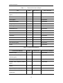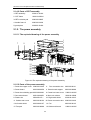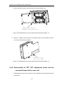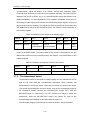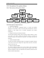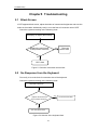
1
DP-6600
Digital Ultrasonic Diagnostic Imaging System
Service Manual
General Description
Contents
INTELLECTUAL PROPERTY STATEMENT ........................................................................... I
RESPONSIBILITYON THE MANUFACTURER PARTY ..................................................................... II
WARRANTY ................................................................................................................................ III
RETURN POLICY ...................................................................................................................... IV
CHAPTER1
GENERAL DESCRIPTION....................................................................... 1-1
1.1
INTRODUCTION ...................................................................................................... 1-1
1.2
PREPARATION FOR REPAIR ..................................................................................... 1-3
1.3
SCHEMATIC DIAGRAM ........................................................................................... 1-5
CHAPTER2
2.1
STRUCTURE OF THE COMPLETE MACHINE & DISASSEMBLY. 2-1
STRUCTURE OF THE COMPLETE MACHINE ............................................................. 2-1
2.1.1.
The appearance view of the main unit ...........................................................................2-1
2.1.2.
The exploded drawing of the complete machine............................................................2-1
2.1.3.
The keyboard assembly ..................................................................................................2-3
2.1.4.
The exploded drawing of CRT assembly .......................................................................2-4
2.1.5.
The power assembly.......................................................................................................2-5
2.2
DISASSEMBLY ........................................................................................................ 2-6
2.2.1.
Disassembly of the rear cover ........................................................................................2-6
2.2.2.
Disassembly of the cabinet tail board ............................................................................2-7
2.2.3.
Disassembly of the cabinet rear cover............................................................................2-8
2.2.4.
Disassembly of the power board ....................................................................................2-9
2.2.5.
Disassembly of the main board and the transducer board ............................................2-10
2.2.6.
Disassembly of CRT, CRT adjustment board and the connection board of the main unit
2-13
2.2.7.
Disassembly of CRT screen filter .................................................................................2-16
2.2.8.
Disassembly of the keyboard, trackball and buzzer .....................................................2-16
2.2.9.
Disassembly of the fan .................................................................................................2-20
2.2.10.
Remove USB extension wire .......................................................................................2-20
CHAPTER3
3.1
DESCRIPTION OF THE PRINCIPLE .................................................... 3-1
THE PRINCIPLE OF THE HARDWARE ....................................................................... 3-1
3.1.1.
The power board ............................................................................................................3-1
3.1.2.
The connection board .....................................................................................................3-5
3.1.3.
The transducer board ....................................................................................................3-10
3.1.4.
The main board ............................................................................................................ 3-11
i
General Description
3.1.5.
The keyboard................................................................................................................3-15
3.1.6.
CRT display..................................................................................................................3-16
3.1.7.
Field tuning after replacing the board ..........................................................................3-16
PRINCIPLE OF THE SOFTWARE .............................................................................. 3-17
3.2
3.2.1.
Features and functions of the real-time operating system ............................................3-17
3.2.2.
Description of the system software ..............................................................................3-18
3.2.3.
Software upgrading procedure .....................................................................................3-20
CHAPTER4
4.1
SYSTEM START-UP .................................................................................. 4-1
SYSTEM START-UP ................................................................................................. 4-1
CHAPTER5
TROUBLESHOOTING.............................................................................. 5-1
5.1
BLACK SCREEN...................................................................................................... 5-1
5.2
NO RESPONSE FROM THE KEYBOARD .................................................................... 5-1
5.3
NO ECHO SIGNAL IN IMAGE AREA ......................................................................... 5-2
5.4
BLACK AREA IN THE IMAGE(BLACK STRIP) ..................................................... 5-3
5.5
IMAGE INTERFERENCE ........................................................................................... 5-3
5.6
BACK-END CIRCUITS FAULT .................................................................................. 5-4
5.7
OTHER FAULTS ...................................................................................................... 5-4
CHAPTER6
6.1
MAINTENANCE AND CLEANING ........................................................ 6-1
MAINTENANCE TO BE PERFORMED BY USER ........................................................ 6-1
6.1.1.
Cleaning the system .......................................................................................................6-1
6.1.2.
Creating a backup copy of the system hard disk ............................................................6-3
6.2
MAINTENANCE TO BE PERFORMED BY SERVICE PERSONNEL ............................... 6-3
APPENDIX A ELECTRICAL SAFETY INSPECTION .........................................................A-1
ii
General Description
© 2005-2012 Shenzhen Mindray Bio-medical Electronics Co., Ltd. All Rights Reserved.
For this Service Manual, the issued Date is 2012-09.
Intellectual Property Statement
SHENZHEN MINDRAY BIO-MEDICAL ELECTRONICS CO., LTD. (hereinafter called Mindray)
owns the intellectual property rights to this Mindray product and this manual. This manual may
refer to information protected by copyrights or patents and does not convey any license under
the patent rights of Mindray, nor the rights of others. Mindray does not assume any liability
arising out of any infringements of patents or other rights of third parties.
Mindray intends to maintain the contents of this manual as confidential information. Disclosure
of the information in this manual in any manner without the written permission of Mindray is
strictly forbidden.
Release, amendment, reproduction, distribution, rent, adaptation and translation of this
manual in any manner whatsoever without the written permission of Mindray is strictly
forbidden.
,
,
,
,
,
are the registered
trademarks or trademarks owned by Mindray in China and other countries.
All other
trademarks that appear in this manual are used only for editorial purposes without the intention
of improperly using them. They are the property of their respective owners.
I
General Description
Responsibility on the Manufacturer Party
Contents of this manual are subject to changes without prior notice.
All information contained in this manual is believed to be correct. Mindray shall not be
liable for errors contained herein nor for incidental or consequential damages in
connection with the furnishing, performance, or use of this manual.
Mindray is responsible for safety, reliability and performance of this product only in the
condition that:
• all installation operations, expansions, changes, modifications and repairs of this product
are conducted by Mindray authorized personnel;
• the electrical installation of the relevant room complies with the applicable national and local
requirements;
• the product is used in accordance with the instructions for use.
Upon request, Mindray may provide, with compensation, necessary circuit diagrams,
calibration illustration list and other information to help qualified technician to maintain and
repair some parts, which Mindray may define as user serviceable.
Note
This equipment is not intended for family usage.
This equipment must be operated by skilled/trained medical professionals.
Warning
It is important for the hospital or organization that employs this equipment to carry out a
reasonable service/maintenance plan. Neglect of this may result in machine breakdown or
injury of human health.
II
General Description
Warranty
THIS WARRANTY IS EXCLUSIVE AND IS IN LIEU OF ALL OTHER WARRANTIES,
EXPRESSED OR IMPLIED, INCLUDING WARRANTIES OF MERCHANTABILITY OR
FITNESS FOR ANY PARTICULAR PURPOSE.
Exemptions
Mindray's obligation or liability under this warranty does not include any transportation or
other charges or liability for direct, indirect or consequential damages or delay resulting
from the improper use or application of the product or the use of parts or accessories not
approved by Mindray or repairs by people other than Mindray authorized personnel.
This warranty shall not extend to:
Any Mindray product which has been subjected to misuse, negligence or accident;
Any Mindray product from which Mindray's original serial number tag or product
identification markings have been altered or removed;
Any product of any other manufacturer.
Safety, Reliability and Performance
Mindray is not responsible for the effects on safety, reliability and performance of the product if:
Assembly operations, extensions, re-adjusts, modifications or repairs are carried out by
persons other than those authorized by Mindray.
Personnel unauthorized by Mindray repairs or modifies the instrument.
III
General Description
Return Policy
Return Procedure
In the event that it becomes necessary to return this product or part of this product to Mindray,
the following procedure should be followed:
1.
Obtain return authorization: Contact the Mindray Service Department and obtain a
Customer Service Authorization (Mindray) number. The Mindray number must appear on
the outside of the shipping container. Returned shipments will not be accepted if the
Mindray number is not clearly visible. Please provide the model number, serial number,
and a brief description of the reason for return.
2.
Freight policy: The customer is responsible for freight charges when this product is
shipped to Mindray for service (this includes customs charges).
3.
Return address: Please send the part(s) or equipment to the address offered by Customer
Service department
Company Contact
Manufacturer:
Address:
Shenzhen Mindray Bio-Medical Electronics Co., Ltd.
Mindray Building, Keji 12th Road South, Hi-tech Industrial
Park, Nanshan, Shenzhen,518057, P.R.China
Phone:
+86 755 26582479 26582888
Fax:
+86 755 26582934 26582500
EC-Representative:
Address:
Phone:
Fax:
Shanghai International Holding Corp. GmbH(Europe)
Eiffestrasse 80, 20537 Hamburg Germany
0049-40-2513175
0049-40-255726
IV
General Description
Safety Precautions
1. Meaning of Signal Words
In this operation manual, the signal words
DANGER,
WARNING,
CAUTION and NOTE are used regarding safety and other important instructions.
The signal words and their meanings are defined as follows. Please understand their
meanings clearly before reading this manual.
Signal word
Meaning
DANGER
Indicates an imminently hazardous situation which, if not
avoided, will result in death or serious injury.
WARNING
Indicates a potentially hazardous situation which, if not
avoided, could result in death or serious injury.
CAUTION
Indicates a potentially hazardous situation which, if not
avoided, may result in minor or moderate injury.
NOTE
Indicates a potentially hazardous situation which, if not
avoided, may result in property damage.
2. Meaning of Safety Symbols
Symbol
Description
Type-BF applied part
NOTE :All ultrasound transducers can be connected to this system
are Type-BF applied part.
"Attention" indicates the points requiring attention. Be sure to read
the operation manual concerning these points before using the
equipment.
V
General Description
3. Safety Precautions
Please observe the following precautions to ensure patient and operator safety when
using this system.
CAUTION: 1. Display the most suitable image and select the most suitable
measurement mode for the intended measurement. The results
must be determined by a specialist.
2. The basic measurement results are not displayed in the exam
report.
3. Be sure to perform measurement within images. If the area is
outside the image, incorrect diagnosis may result.
4. The detailed precautions for each measurement are described
in the corresponding section. Read and understand these
precautions before performing the measurement.
5. Data in temporary storage areas, such as the CINE memory, is
deleted when the power supply is turned OFF or when the
Patient switch is pressed. Such data may also occasionally be
deleted due to accidents. To minimize the possibility of
reexamination being required as a result of unintended data
deletion, back up the required images on external storage
media.
6. Refer to the Operation Manual (Fundamentals) for precautions
regarding the use of this system.
VI
General Description
Chapter1 General Description
1.1
Introduction
DP-6600 is a portable digital diagnostic ultrasound system, which features black &
white imaging.
1. Front view
Power indicator
Air inlet
Figure 1-1 Front view
2. Rear view
1-1
General Description
Handle
Gel cup holder
Transducer holder
CRT vent
grounding pole
Power inlet
Transducer cable
hook
Power switch
Winding rack
Main unit vent
ain unit vent
Network interface
Printer interface
Video interface
Figure 1-2 Rear view
3. Left view
USB interface
Figure 1-3 Left view
1-2
General Description
4. Right view
Transducer
socket
Figure 1-4 Right view
5. Elevation view(with the keyboard unfolded)
Figure 1-5 Elevation view(with the keyboard unfolded)
1.2
Preparation for Repair
The needed tools and measurement devices are shown as followed:
1-3
General Description
Table 1-1
Tool
Tools and Devices for Repair
Model
Manufacturer
Screwdriver (various sizes and
Spec./Standard
Unspecified
types)
Flat-headed screwdriver (large)
Unspecified
Wire nippers
Unspecified
Needle nose pliers
Unspecified
Diagonal pliers
Unspecified
Soldering iron and stand
Unspecified
Desoldering tool
Unspecified
Wrench set
Unspecified
Adjustable wrench
Unspecified
Tweezers
Unspecified
Hammer
Unspecified
Metric Allen wrench set
Unspecified
File (various types)
Unspecified
Cutter
Unspecified
Table 1-2 Consumable Material
Consumable Material
Model
Insulation tape
Hishilite
tube,
Manufacturer
Specification/Standard
Unspecified
Empire
tube
Unspecified
(various types)
Wires (various types)
Unspecified
Screws, nuts, washers (various
Unspecified
types)
Solder
Paper file (various types)
Ethanol
for
cleaning
and
disinfection
1-4
General Description
1.3
Schematic Diagram
Figure 1-6 Schematic Diagram
1-5
Structure of the Complete Machine & Disassembly
Chapter2 Structure of the Complete Machine &
Disassembly
2.1 Structure of the Complete Machine
2.1.1. The appearance view of the main unit
1
1.Main unit 2300-30-29157
Figure 2-1 The appearance view of the main unit
2.1.2. The exploded drawing of the complete machine
2.1.2.1. The exploded drawing of the complete machine
7
8
9
10
11
Refer to the
figure below 2 3 4 5 6
12
Refer to the figure below
13
14
1
Refer to the figure below
20
19
18
17
15
16
Figure 2-2 The exploded drawing of the complete machine
2-1
Structure of the Complete Machine & Disassembly
2.1.2.2. Parts of each assembly
1. CRT knob
2300-20-29084
2. screen filter fixing buckle
9901-20-23950
3. screen filter
2102-20-16994
4. keyboard hook
2300-20-29092
5. front cover
2300-20-29078
6.
2300-20-29091
keyboard protective pad
7. handle rubber cap A
2300-20-29089
8. handle rubber cap B
2300-20-29090
9. handle
2300-20-29081
10. transducer holder
2300-20-29082
11. rear cover
2300-20-29079
12. transducer cable hook
2102-30-16949
13. winding rack
2300-20-29083
14. winding rack rubber cap
2300-20-29088
15. hook holder
2300-20-29085
16. bottom rubber pad
2300-20-29087
17. bottom plate
2300-20-29080
18. USB cable
2300-20-29138
19. conductive cloth
9901-10-23920
20. USB compressor
2300-20-29106
2-2
Structure of the Complete Machine & Disassembly
2.1.3. The keyboard assembly
2.1.3.1. The exploded drawing (1) of the keyboard assembly
3
4
5
6
7
1
9
10
11
8
2
Figure 2-3 The exploded drawing (1) of the keyboard assembly
2.1.3.2. Parts of the keyboard assembly (1)
1. keyboard upper cover assembly 2300-30-29156
2. keyboard lower cover assembly 2300-30-29155
3. keyboard knob C
2300-20-29073
4. keyboard silicon cap
2300-20-29076
5. keyboard DIP switch
2300-20-29074
6. keyboard knob B
2300-20-29072
7. keyboard knob A
2300-20-29071
8. hollow shaft
2300-20-29067
9. position limiter
2300-20-29066
10. compressing spring
2300-20-29065
11. keyboard buckle
2300-20-29064
2-3
Structure of the Complete Machine & Disassembly
2.1.3.3. The exploded drawing (2) of the keyboard assembly
1
2
3
6
4
5
Figure 2-4 The exploded drawing (2) of the keyboard assembly
2.1.3.4. Parts of the keyboard assembly (2)
1. keyboard upper cover
2300-30-29156
2. dust plate
2300-20-29075
3. buzzer
2300-21-29142
4. silicon key
2300-20-29060
5. keyboard PCB board
2300-20-29057
6. trackball
0000-10-10893
2.1.4. The exploded drawing of CRT assembly
2.1.4.1. The exploded drawing of CRT assembly
1
2
3
Figure 2-5 The exploded drawing of CRT assembly
2-4
4
5
Structure of the Complete Machine & Disassembly
2.1.4.2. Parts of CRT assembly
1.CRT assembly
2300-21-29149
2. CRT frame
2300-20-29094
3.CRT insulation pad
2300-20-29095
4. handle frame 2
2300-20-29108
5.guard plate
2300-20-29109
2.1.5. The power assembly
2.1.5.1. The exploded drawing of the power assembly
7
8
1
2
3
4
5
6
9
10
11 12 13 14 15 16 17 1819
24
25
26
27
28
29
20
21
22
23
Figure 2-6 The exploded drawing of the power assembly
2.1.5.2. Parts of the power assembly
1. Power box upper cover 2300-20-29194
2.
3. Power board
4. Power board support
2300-30-29059
Fan connection wire 2300-20-29141
2300-20-29098
5. Power box shielding pad 2300-20-29202
6. Power box lower cover 2300-20-29195
7.Connection board
2300-30-29053
8. Main unit cabinet
2300-20-29096
9. Plastic slot
M90-000115---
10. Right wind shield
2300-20-29113
11. Cabinet rear cover
2300-20-29104 12.Power connection wire 2300-20-29140
13.Left wind shield
2300-20-29107
14. Fan
15. Fan pad
2300-20-29099
16.Cabinet tail board
2-5
2300-20-29143
2300-20-29105
Structure of the Complete Machine & Disassembly
17. Grounding pole
0509-20-00098
18.Power socket
19. Power switch
2100-10-07943
20. Main board connector 2300-20-29208
21.Main board
2300-30-29051
22.Main board support
23. Conductive cloth
9901-10-23920
24.Transducer board shield cover
2300-20-29198
25.Transducer board
2300-30-29055
26. Transducer socket fixed plate
2300-20-29101
27. Shield spring A
2102-20-16918
28. Shield spring B
2102-20-17113
29. Transducer socket fastener
2300-20-29199
2.2 Disassembly
2.2.1. Disassembly of the rear cover
1.
Removing the transducer cable hook
(1)
(2)
Figure 2-7 Disassembly of the rear cover
A、 Turn the transducer cable hook clockwise to the end;
B、 Take out the transducer cable hook upward.
2.
Removing the handle and winding rack
2-6
2300-21-29147
2300-20-29110
Structure of the Complete Machine & Disassembly
M4x16 Screw
Handle
rubber
Handle
cap A
rubber
cap B
M4x12 Screw
Winding rack rubber cap
Figure 2-8 Removing the handle and winding rack
3.
A.
Pull out the handle rubber cap A&B and the winding rack rubber cap;
B.
Remove the two M4x16 fixing screws, and then take out the handle
C.
Remove the two M4x12 fixing screws, and then take out the winding rack
Removing the rear cover
(1)
Figure 2-9 Removing the rear cover
A. lift the tail of the rear cover forcibly;
B. Move the rear cover backwards to remove it.
2.2.2. Disassembly of the cabinet tail board
1.
Remove the rear cover;
2.
Disconnect the fan connector of the tail board;
3.
Remove 8 M3X6 screws fixing the tail board and 2 M3X6 screws fixing the main
2-7
Structure of the Complete Machine & Disassembly
board;
4.
Disconnect the power wire connector and move the tail board backward to take it
out.
power wire connector
Fan connector
2 Fixing screws of
the main board(M3X6)
8 Fixing screws of
the tail board(M3X6)
Figure 2-10 Disassembly of the cabinet tail board
2.2.3. Disassembly of the cabinet rear cover
1.
Remove the assembly of the cabinet tail board;
2.
Disconnect the fan connector of the rear cover;
3.
Remove 9 M3X6 screws fixing the rear cover and take out the rear cover.
Fan connector
9 fixing screws(M3X6)
Figure 2-11 Disassembly of the cabinet rear cover
2-8
Structure of the Complete Machine & Disassembly
2.2.4. Disassembly of the power board
1.
Remove the assembly of cabinet rear cover;
2.
Pull out the assemble of the power board;
le
semb
e as d
h
t
out er boar
w
Pull
e po
h
of t
Figure 2-12 Disassembly of the power board
3.
Remove 6 M3X6 screws fixing the power box upper cover, and open the upper
cover;
4.
Disconnect the fan connector of the power board;
6 screws fixing the
upper cover(M3X6)
Fan connector
Figure 2-13 Disconnecting the fan connector
5.
Remove 7 M3X8 screws fixing the power board and take out the power board;
2-9
Structure of the Complete Machine & Disassembly
7 M3X8 screws fixing
the power board
Power board
Power board
shielding pad
Power board
lower cover
Figure2-14 Disassembly of the power board
2.2.5. Disassembly of the main board and the transducer
board
1.
Disassemble the rear cover to take out the assemblies of the tail board and the
back board;
2.
Remove 3 M3X8 screws fixing the holder of the transducer cable hook and take
out the holder;
3 Fixing screws
(M3X8)
Holder
USB wire
connector
Figure 2-15 Remove the holder of the transducer cable hook
3.
Remove the USB wire connector;
2-10
Structure of the Complete Machine & Disassembly
4.
Remove 8 M3X6 screws fixing the holder and one M3X6 screw fixing the main
board;
8 M3X6 screws fixing the
transducer socket
Figure 2-16 Disassembly of the main board and the transducer board(1)
Pu
l
bo l o
ar
ut
d
a n th e
d
th ass
e
tr em b l
an
sd ie s
uc
er o f t
bo he
ar
ma
d
i
ba n
ck
wa
r
Figure 2-17 Disassembly of the main board and the transducer board(2)
5.
Pull out the assemblies of the main board and the transducer board backward;
2-11
d
Structure of the Complete Machine & Disassembly
Pul
boa l ou
rd t t
and he
the asse
tra mbli
nsd es
uce of
r b the
oar ma
d b in
ack
war
d
Figure 2-18 Disassembly of the main board and the transducer board(3)
6.
Remove 7 M3X6 screws connecting the assemblies of the main board and the
transducer board, and disassemble the main board;
7 M3X6 connecting screws
Figure 2-19 Disassembly of the main board and the transducer board(4)
2-12
Structure of the Complete Machine & Disassembly
7.
Remove 8 M3X6 screws fixing the transducer board shield cover;
7 M3X6 screws fixing the
transducer board shield cover
Figure 2-20 Disassembly of the main board and the transducer board(5)
8.
Remove 4 M3X6 screws fixing the connection board of the transducer socket,
and remove the transducer board;
4 M3X6 screws fixing
the connection board
Figure 2-21 Disassembly of the main board and the transducer board(6)
2.2.6. Disassembly of CRT, CRT adjustment board and the
connection board of the main unit
1.
Disassemble the rear cover to take out the assemblies of the tail board and the
back board;
2-13
Structure of the Complete Machine & Disassembly
2.
Remove 4 PT4X14 screws fixing the front cover;
4 PT4X14 screws fixing
the front cover
Figure 2-22 Remove 4 PT4X14 screws fixing the front cover
3.
Disconnect CRT signal cable, keyboard connection wire, CRT power wire and
CRT adjustment board connector;
CRT signal
cable
CRT power
wire
Keyboard
connection wire
Figure 2-23 Disconnect the connection wires
2-14
CRT adjustment
board connector
Structure of the Complete Machine & Disassembly
4.
Remove 8 M3X8 screws fixing CRT assembly and take out CRT;
8 M3X8 screws
fixing CRT assembly
Figure 2-24 Remove CRT assembly
5.
Remove CRT adjustment knobs and 4 PT3X8 screws fixing CRT adjustment
board, and then remove the CRT adjustment board;
CRT adjustment
knobs
4 PT3X8 screws
fixing CRT
adjustment board
Figure 2-25 Remove CRT adjustment knobs
6.
Remove 8 M3X6 screws fixing the connection board of the main unit, and then
2-15
Structure of the Complete Machine & Disassembly
remove the connection board of the main unit.
8 M3X6 screws
fixing the
connection board
Figure 2-26 Remove the connection board of the main unit
2.2.7. Disassembly of CRT screen filter
1.
Slide the two screen filter buckles outward and pull them out;
2.
Pull out the upper screen filter outward and uplift it, and then take it out.
(3)
(1)
(1)
(2)
(4)
(2)
Figure 2-27 Disassembly of CRT screen filter
2.2.8. Disassembly of the keyboard, trackball and buzzer
1.
Remove the two keyboard silicon caps, and then remove 2 M3×6 screws fixing
the keyboard upper cover;
2-16
Structure of the Complete Machine & Disassembly
Two keyboard silicon caps
2 M3x6 screws
Figure 2-28 Remove the two keyboard silicon caps and two screws
2.
Open the keyboard upper cover by hands forcibly at the positions of arrows;
keyboard upper
cover assembly
keyboard
lower
cover assembly
Figure 2-29 Disassembly of the keyboard upper cover
2-17
Structure of the Complete Machine & Disassembly
3.
Disconnect the connection wire connector of the keyboard, and remove the
keyboard upper cover;
Keyboard connection wire
Figure 2-30 Disassembly of the keyboard upper cover
4.
Disconnect the connection wire connector of the trackball, remove 4
self-threading ST3x14 screws fixing the trackball, and remove the trackball;
Connection wire of the trackball
4 self-threading screws
Figure 2-31 Disassembly of the trackball
2-18
Structure of the Complete Machine & Disassembly
5.
Pull out keyboard knobs A, B, C and 6 keyboard DIP switches;
keyboard knob C
6 keyboard DIP
switches
keyboard knob D
keyboard knob B
keyboard knob A
Figure 2-32 Remove the keyboard knobs and switches
6.
Disconnect the connection wire connector of the buzzer, remove 14 ST3x8
screws fixing the keyboard, remove the silicon keys to take out keyboard PCB
board, and remove 2
ST2x6 screws fixing the buzzer to take out the buzzer.
ST3x8 screws(14)
Keyboard
Connection wire
PCB
of the buzzer
Silicon keys
2 ST2x6screws
buzzer
Figure 2-33 Remove the buzzer
2-19
Structure of the Complete Machine & Disassembly
2.2.9. Disassembly of the fan
1.
Remove the rear cover;
2.
Disconnect the tail board fan connector and remove 4 M3X30 screws, and then
remove the tail board fan;
4 M3X30 Screws
fixing the fan
Fan pad
Fan
Figure 2-34 Disassembly of the tail board fan
3.
Disconnect the back board fan connector and remove 8 M3X30 screws, and then
remove the back board fan.
8 M3X30 Screws
fixing the fan
Fan pads
Fan
Figure 2-35 Disassembly of the back board fan
2.2.10.
1.
Remove USB extension wire
Disassemble the rear cover, the cabinet tail board assembly, the cabinet back
board assembly and the front cover assembly;
2-20
Structure of the Complete Machine & Disassembly
2.
Remove 7 PT3x8 screws fixing the cabinet bottom board, and remove the
cabinet;
7 PT3x8 screw
Figure 2-36 Disassemble the cabinet
3.
Remove 2 PT3x 8 screws fixing USB compressor, and remove USB compressor,
and then take out USB extension wire.
PT3x8 screw
USB compressor
Figure 2-37 Remove USB extension wire
2-21
Description of the Principle
Chapter3 Description of the Principle
3.1 The Principle of the Hardware
3.1.1. The power board
3.1.1.1. Description of the power board
The power system is designed to supply power for the overall ultrasound
diagnostic system, and it can supply nine static DC outputs, including the +5V
( D+5V and A+5V ) , -5V, +12V, +13.5V, +3.3V, +1.5V, +2.5V and
program-controlled high voltage outputs.
The performance specifications for each output are shown in Table 3-1.
Table 3-1 the specifications for the power board outputs
Item
Rated
Voltage
Voltage
Precision
Rated
Load
(V)
)
1
3A
A+5V
Mini
mum
Load
Voltag
e
Adjust
ment
Rate
Load
Adjust
ment
Rate
Ripple
Noise
Use
(mVpk-pk)
0.5A
Analog
circuits/keyboard
2
D+5V
3.5A
1.0A
3
-5.0V
0.4A
20m
<30mV
Keyboard /USB
Amplifier
A
4
+13.5V
5
+12V
±5%
1.5A
0.3A
0.35A
100
VGA
<2%
<50mV
mA
6
HV
50mA
Fan /CMOS
<5%
0
devices
Transmission
circuit
7
+3.3V
3.5A
0.2A
8
+2.5V
1.0A
0.2A
9
+1.5V
2.0A
0.2A
Digital circuits
<30mV
Digital circuits
Digital circuits
3.1.1.2. The basic principle
The schematic diagram of the power board is shown in Figure 2-1.
As shown in the figure, the power board is comprised of the input circuit, PFC front
3-1
Description of the Principle
end, FORWARD converter and back stage DC-DC converter circuits. The AC
input first goes through the EMI filter and surge suppression circuit, and then the
BOOST APFC circuit to have the power factor corrected and to provide a stable
390V DC voltage to the FORWARD converter. The FORWARD converter provides 4
outputs, +5V, -5V, +13.5V and +24V. The 24V output serves as the input of the HV
output of the power board. The +13.5V output passes two diodes to generate the
+12V output of the power board. The +5V output serves two purposes: 1) to be
divided into the A+5V and D+5V outputs of the power board; 2) to serve as the input
to the back stage DC-DC converters to generate the +3.3V, +2.5V and +1.5V
outputs of the power board.
The PFC circuit adopts the TI UC3854 as the control chip and incorporates the
BOOST converter. The main switching transistor and free wheeling diode used are
the IR IRFPC60LC and the FAIRCHILD ISL9RL1560G2, whose parameters are
600V/16A and 600V/15A respectively.
EMI
FILTER &
AC
INPUT INRUSH
LIMIT
FORWARD
CONVERTOR
BOOST
APFC
STAGE
LINEAR
REGULATOR
- 5V
OCP/OVP
MAGNETIC
AMPLIFIER
+ 13 .5V
OVP &
OTP
2
+1 2V
LINEAR
REGULATOR
BOOST
CONVERTOR
HV
OCP/OVP
3
1
VOLTAGE
CONVERTING
PWM
CONTROLLER
HVC
A +5 V
+5 V
D +5 V
FEEDBACK
PHOTOCOUPLER
OCP &
OVP
BUCK
CONVERTOR
+3 .3 V
LINEAR
REGULATOR
+2 .5 V
BUCK
CONVERTOR
+1 .5 V
Figure 3-1 the schematic diagram of the power board
3-2
Description of the Principle
The FORWARD converter adopts the FUJITSU MB3769A as the control chip. The
transformer T1 transforms the AC voltage into the DC voltage and isolates the former
from the latter, making the system safe. The NEC 2SK2485 is used as the switching
transistor, whose parameter is 900V/6A. The main feedback output of the FORWARD
converter is +5V. The +13.5V output of the FORWARD converter is first stabilized by
the magnetic amplifier and then serves as the +13.5V output of the power board. The
-5V output of the FORWARD converter is first stabilized and then serves as the -5V
output of the power board.
The BOOST converter, using the ON-SEMI TL594 as the control chip, converts the
24V output of the FORWARD converter into the HV output of the power board. An
analog signal that varies between 0 to 4V controls the HV output, the latter varying
linearly with the change of the former.
The BUCK converters, using the INTERSIL EL7566 as the control chips, are used to
generate the +3.3V and +1.5V outputs of the power board. The +3.3V output is also
passed to a linear stabilizer, which is composed of discrete devices, to generate the 2.5V
output of the power board.
The power board features the over-voltage protection for the PFC output, the
over-temperature protection, the over-voltage /over-current /short-circuit protection for
the +5V output, the over-voltage /over-current /short-circuit protection for the +13.5V
output, the over-voltage /over-current /short-circuit protection for the HV output, and
the short-circuit protection for all other outputs. Once the protections are tripped, the
power board reacts as follows:
1.
When the over-voltage protection for the PFC output, over-temperature
protection or the over-voltage /over-current /short-circuit protection for the +5V
output is tripped, the power board cuts off all the outputs and keeps them locked.
Only after the AC input is cut off and the fault is cleared and the system is reset,
does the system return to normal work;
2.
When the over-voltage /over-current /short-circuit protection for the +13.5V
output is tripped, both the +13.5V output and the HV output are cut off and remain
locked. After the fault is cleared and all loads are disconnected from the +13.5V
output, both the outputs will resume;
3.
When the short-circuit protection for the +3.3V output is tripped, both the +3.3V
output and the HV output are cut off. After the fault is cleared, both the outputs will
resume;
3-3
Description of the Principle
4.
When the over-voltage /over-current /short-circuit protection for the HV output,
over-current /short-circuit protection for the -5V output, short-circuit protection for
the +1.5V output, or the over-current /short-circuit protection for +2.5V output is
tripped, the faulty output will be cut off independently without affecting any normal
output. After the fault is cleared, all the outputs return to normal work automatically,
except the HV output remains locked.
3.1.1.3. Maintenance of the power board
Before tested, the power board should be connected as per Figure3-2. In the
figure, the load A is a must, while the load B depends on situations. Under some
conditions, for the purpose of easy repair, the load B is not allowed to exceed 0.1A,
and it should be applied only when other outputs are minimum.
390V
DCAC INPUT
LOAD B
POWER SUPPLY
LOAD A
(AT LEAST THREE
MODULES)
Figure 3-2 Connection schematic of the power board for testing
Based on your own needs, you can connect the loads only to the +5V, +13.5V and
HV outputs. For the purpose of easy adjustment, it is recommended that the
adjustment starts with a load slightly greater than the minimum load, and the load
can be increased according to practical situations during adjustment.
After the power board is correctly connected, follow the flow chart indicated in
Figure3-3 to find and fix the faults.
3-4
Description of the Principle
switch on AC
input.
Y
Is +5V output
Is +13.5V output
Y
normal?
normal?
N
Check if U3, Q4,
T1 and R66 are
normal.
Y
Y
Is end voltage of
Is +3.3V output
C12 390Vdc?
normal?
Y
N
Check the OTP
检查
OTP、
及+5V
输
circuit
and
OCP,
OVP
circuit
of 电路
+5V
出 OCP
和 OVP
output.
Y
Check the OVP circuit
of PFC output, C23, Y
C24, R30 and
feedback resistor, etc.
N
Check +13.5V circuit,
especially the discrete
devices L11, ZD5 and
U7, etc.
N
Check +3.3V circuit,
especially the discrete
devices U16, C133,
etc.
Check and test
other output
circuits
respectively
Is there a positive
pulse voltage
exceeding 2V for the
anode of D15 or D16
at power-on instant?
N
Is there a positive pulse
exceeding 2V for the
anode of D14 at
power-on instant?
N
Check U1 and the
components around it Y
and L5, Q1, D2, etc.
Does the maximum end
voltage of C25 exceed
14.5V at power-on instant?
N
Check & replace D44,
ZD1, U1, startup resistor,
Q2, Q3 and fuse, etc.
End.
Figure 3-3 Trouble-shooting flow chart for the power board
3.1.2. The connection board
The connection board is designed for connecting the main board, power board,
keyboard and monitor. See Figure 3-4 for the connections.
3-5
Description of the Principle
MainBoard
Power
Power
Power
Probe
Board
User
Interface
VGA UART
+5V
Connection Board
UART
+13.5V
VGA
Key
Board
Monitor
Figure 3-4 Interconnection of the system
The signals of the connection board are defined as follows:
Table 3-2 Definition of the connection board signals
Symbol
Name
Description
NC
Empty
No connection
GND
Ground
Ground, not specified as the analog or digital ground.
PHV
High
voltage
The HV output of the power board, ranging from +30V
pulse
to +140V.
13V5
+13.5V power
The +13.5V output of the power board.
12V
+12V power
The +12V output of the power board.
A+5
+5V
analogue
The A+5V output of the power board.
digital
The D+5V output of the power board.
power
D+5
+5V
power
3V3
+3.3V power
The +3.3V output of the power board.
2V5
+2.5V power
The +2.5V output of the power board.
1V5
+1.5V power
The +1.5V output of the power board.
-5V
-5V power
The -5V output of the power board.
HVC
High
The analog signal that goes from the main board to the
voltage
control
power board to control the HV output and varies
between 0 and 4V.
RxDFromKB
Receive
data
The 5V TTL serial signal from the keyboard to the main
3-6
Description of the Principle
TxDToKB
VS
from keyboard
board.
Transmit data to
The 5V TTL serial signal from the main board to the
keyboard
keyboard.
VGA
HS
B
vertical
The 3.3V COMS signal from the main board to the
synchronization
monitor for VGA vertical synchronization.
VGA horizontal
The 3.3V COMS signal from the main board to the
synchronization
monitor for VGA horizontal synchronization.
VGA
The analog video signal from the main board to the
video
signal
VGA port of the monitor, the maximum value up to 0.7V.
A VME socket, the AMP AMP535043-4, is used for connecting the main board and
the connection board. The main board is connected with the power board through the
connection board, to obtain the powers PHV,-5V, A+5V,2.5V,1.5V,3.3V,12V,
13.5V and D+5V digital. The main board outputs an analog signal, HVC, to control the HV
output of the power board. The serial signals RxDFromKB and TxDToKB are used for the
communications between the main board and keyboard. The main board outputs the VGA
signals HS, VS and B to the monitor. See Table 3-3 Definition of the interface signals
between the main board and the connection board below:
Table 3-4 Definition of the interface signals between the main board and the connection board
A
B
C
1
PHV
PHV
PHV
2
NC
NC
NC
3
GND
GND
GND
4
-5V
-5V
-5V
5
GND
GND
GND
6
12V
12V
12V
7
GND
GND
GND
8
A+5
A+5
A+5
9
A+5
A+5
A+5
10
A+5
A+5
A+5
11
GND
GND
GND
12
HVC
GND
GND
13
GND
GND
GND
14
GND
GND
GND
15
2V5
2V5
2V5
3-7
Description of the Principle
16
GND
GND
GND
17
1V5
1V5
1V5
18
1V5
1V5
1V5
19
GND
GND
GND
20
GND
GND
GND
21
3V3
3V3
3V3
22
3V3
3V3
3V3
23
GND
GND
GND
24
GND
GND
GND
25
13V5
13V5
13V5
26
VS
GND
GND
27
HS
GND
B
28
GND
GND
GND
29
TxDToKB
GND
RxDFromKB
30
GND
GND
GND
31
D+5
D+5
D+5
32
D+5
D+5
D+5
Another VME socket, also the AMP AMP535043-4, is used for connecting the power
board and the connection board. See Table 3-4 for the definition of the interface signals:
Table 3-4 Definition of the interface signals between the power board and the connection board
A
B
C
1
PHV
PHV
PHV
2
NC
NC
NC
3
GND
GND
GND
4
-5V
-5V
-5V
5
GND
GND
GND
6
12V
12V
12V
7
GND
GND
GND
8
A+5
A+5
A+5
9
A+5
A+5
A+5
10
A+5
A+5
A+5
11
GND
GND
GND
12
HVC
GND
GND
13
GND
GND
GND
3-8
Description of the Principle
14
GND
GND
GND
15
2V5
2V5
2V5
16
GND
GND
GND
17
1V5
1V5
1V5
18
1V5
1V5
1V5
19
GND
GND
GND
20
GND
GND
GND
21
3V3
3V3
3V3
22
3V3
3V3
3V3
23
GND
GND
GND
24
GND
GND
GND
25
13V5
13V5
13V5
26
NC
GND
GND
27
NC
GND
NC
28
GND
GND
GND
29
NC
GND
NC
30
GND
GND
GND
31
D+5
D+5
D+5
32
D+5
D+5
D+5
The B8B-PH-K-S made by JST is used for connecting the keyboard and the
connection board, and the interface signals between the two boards are defined in the
table below. The serial communication signals between the keyboard and the main board
are switched through the connection board, with TTL level and baud rate 38400bps; the
+5V power of the keyboard is the D+5V output of the power board, and its current is 2A.
Table 3-5 Definition of the interface signals between the keyboard and the connection board
Position
PIN1
PIN2
PIN3
PIN4
PIN5
PIN
PIN7
PIN8
D+5
D+5
6
Signal
RxDFromKB
GND
TxDToKB
GND
GND
GN
D
Description
From
keyboard
main board
Ground
to
From
main
board
to
Ground
+5V power
keyboard
The signals transmitted from the main board to the monitor are switched through the
connection board. The horizontal synchronization signal HS and the vertical
3-9
Description of the Principle
synchronization signal VS feature 3.3V CMOS, vertical scan frequency 60Hz,
horizontal scan frequency 31.5KHz and non-interlaced scanning. The video signal is
obtained from the B of RGB, and it is a monochromatic signal that features over
40MHz bandwidth, 75Ωinput impedance, 0.7V maximum amplitude. Since the B is
the analogue video signal, which shouldn’t be interfered by digital signals, the ground
wire must be used for shielding. The signal wire from the monitor is connected to the
JST B6B-PH-K-S socket on the connection board. See Table 3-6 for the definition of
the interface signals.
Table 3-6 Definition of the socket of the display signal
Position
PIN1
PIN 2
PIN 3
PIN 4
PIN 5
PIN 6
Signal
GND
HS
VS
GND
GND
B
Description
Ground
Horizontal
Vertical
Ground
Ground
Video
synchronization
synchronization
signal
The monitor obtains the +13.5V power, the current of which is 1.5A, from the 13.5V
output of the power board. The power cable of the monitor is connected to the JST
B4B-PH-K-S socket on the connection board. See Table 3-7 for the definition of the
interface signals.
Table 3-7 Definition of the power socket of the monitor
Position
PIN 1
PIN 2
PIN 3
PIN 4
Signal
GND
GND
13V5
13V5
Description
Ground
13.5V power
3.1.3. The transducer board
The transducer board is designed to switch between the two transducers and to
read the ID code from the corresponding transducer. Relay channels are
incorporated to control the switch, while they are driven by another two relays.
The control signal ENB from the main board, used as the coordinating signal of
the transducer board, controls the 2N7002LT1(an N-type FET) and the
MC74HCT244(an IC component). The FET controls the relays to switch the
transducers, while the MC74HCT244 returns the correct ID code to the
corresponding data interface for the main board to read it out.
The schematic diagram of the transducer board is shown in the figure below:
3-10
Description of the Principle
Figure 3-5 the schematic diagram of the transducer board
3.1.4. The main board
3.1.4.1. Principle description
The main board can realize the functions such as transmission and reception,
beam forming, signal processing, DSC, CINE review, networking, USB, VIDEO
and VGA, etc.
The hardware of the main board supports an transmission circuit, which is divided
into an low-voltage transmission pulse drive circuit and high-voltage transmission
pulse drive circuit. The transmission is realized by the EP1S10 (FPGA of Stratix
series), and its sequence is controlled by the FPGA as well.
The ATGC-DAC circuit mainly uses the DAC to generate the voltage-controlled
signal of the voltage-controlled gain amplifier. In addition, this dual-channel DAC
can also generate a voltage-controlled signal for controlling the PHV variation,
and the input signal of the DAC is provided by EP1S10.
EP1S10F672C7 is the FPGA of the Stratix series made by ALTERA. It features
1M gate, 10,000 LE, 94 512bits RAM blocks, 60 4Kbits RAM blocks, one 512Kbits
RAM block, and six DSP blocks(each DSP block can be configured into one 36×
36 multiplier, four 18×18 multipliers or eight 9×9 multipliers). It also supports
various 3.3V differential I/Os and DDR interface. In the DP-6600, EP1S10F672C7
is the control core for the front end circuit, providing the transmission sequence
control of the transmission circuit, the control of the reception selection circuit, the
gain adjustment control of the voltage controlled gain amplifier, the adjustment
control of PHV, the beam forming logic, the signal processing logic. Moreover, the
3-11
Description of the Principle
phase lock loop output of EP1S10F672C7 provides a 29.5MHz clock for PAL
system VIDEO signal and a 6MHz clock for USB control chip.
probe
B lookup table/
M DSC buffer
High voltage
isolation/ channel
selection
High voltage
driver
DSC buffer
DSC buffer
Low voltage
driver
DSC(EP1K100)
LNA+VCA
ATGCDAC
DSC buffer
DSC buffer
EP1S10
Transmit
timing
Beam former
CPU interface
Signal
processing
BE bus
Image
data
VGA
timing
Echo
data
A/D
Cine memory
Image memory
Post process
(EP1K100)
Graphic memory
Vga2video buffer
Post process FPGA
configuration
Other FPGA
configuration
Data bus
Address bus
FLASH
CPU(MCF5307)
SDRAM
CPLD
Control bus
I2C
NET interface
Power
monitor
A/D
WDO&E
EPROM
Temperatur
e monitor
RTC
USB
interface
VIDEO
DAC
Power
UART1
Key
board
REMOTE
REMOTE
NET
USB
USB1
NET
USB
USB2
driver
VIDEO1
VGA
DAC
driver
VIDEO2
VGA
Figure 3-6 the schematic diagram of the main board
The CINE review and post-processing functions are realized within one FPGA,
which is the ACEX1K100FC484 made by ALTERA. The chip has two SDRAM used
for CINE review memory, and four SRAM respectively used for frame correlation
buffer, graphics memory, image memory and video signal buffer, thus generating
3-12
Description of the Principle
the signals of frame correlation, graphics circuit, image storage VGA and VIDEO. In
addition, this FPGA chip can also generate the horizontal and vertical
synchronization signals for the VGA monitor and the control signal for the video
printer.
The function of the DSC circuit is realized in one FPGA, which is the
ACEX1K100QC208 made by ALTERA. The chip has one 256k×16 SRAM used for
the B-type DSC look-up table and the M-type memory, and four 128k×8 SRAMs
used for the B-type DSC memory.
The chip MCF5307, made by Motorola, is used as CPU and the control core of the
DP-6600. The chip has SDRAM and FLASH as internal memory and Boot ROM,
and it is externally connected with power detection A/D, watchdog, real-time clock
and temperature detection circuit through IIC bus. The serial port for
communicating with the keyboard is provided by the CPU.
The chip CPLD provides the interfaces between the CPU and the external circuits,
including the USB control interface, network control interface and FPGA
configuration interface, etc.
The DP-6600 has two video DACs, one for generating the monochromatic VGA
signal, the other for generating the video signal. Since the system needs two video
signal outputs, there are two operational amplifiers.
The chip for network interface provides the functions of MAC and PHY, and it is
externally connected with a network transformer to isolate the network signal.
The chip for USB interfaces controls the two USB interfaces and is connected with
an external power management chip. Each USB interface can provide maximum
500mA. If the current exceeds 500mA, the power for USB interfaces will be cut off
automatically.
3.1.4.2. Definition of the main board socket
The socket P2 for connecting the main board and the transducer board is defined
in the table below:
Table 3-8 Definition of the socket for connecting the main board and the transducer board
1
2
3
4
5
6
7
8
9 10 11 12 13 14 15 16 17 18 19 20 21 22 23 24 25 26 27 28 29 30 31 32
A
G
3
6
G 11 14 G 19 22 G 27 30 G 35 38 G 43 46 G 51 54 G 59 62 G 67 70 G 75 78 ID3 ID0
B
1
4
7
9 12 15 17 20 23 25 28 31 33 36 39 41 44 47 49 52 55 57 60 63 65 68 71 73 76 79 ENB ID1
C
2
5
8
10 13 16 18 21 24 26 29 32 34 37 40 42 45 48 50 53 56 58 61 64 66 69 72 74 77 80 +5 ID2
A VME socket is adopted for connecting the main board and the transducer board,
and it is the 650947-5 made by AMP.
3-13
Description of the Principle
In the table. G represents the analogue ground, and the +5V the A +5V power, and
ID0 to ID3 represent the ID codes of the transducer board output. ENB is the
transducer’s selection signal from the main board, when ENB is low, the transducer A
is selected and its ID code of the transducer A is the output; when ENB is high, the
transducer B is selected and its ID code is the output.
The socket P4 for connecting the main board and the connection board is defined in
the table below:
Table 3-5 Definition of the socket for connecting the main board and the connection board
1
2
3
4
5
6
7
8
9 10 11 12 13 14 15 16 17 18 19 20 21 22 23 24 25 26 27 28 29 30 31 32
A PHV NC G -5V G 12V G A+5 A+5 A+5 G HVC G
G 2V5 G 1V5 1V5 G
G 3V3 3V3 G
G 13V5 VS HS G TXD G D+5 D+5
B PHV NC G -5V G 12V G A+5 A+5 A+5 G
G
G
G 2V5 G 1V5 1V5 G
G 3V3 3V3 G
G 13V5 G
G
G
C PHV NC G -5V G 12V G A+5 A+5 A+5 G
G
G
G 2V5 G 1V5 1V5 G
G 3V3 3V3 G
G 13V5 G
B
G RXD G D+5 D+5
G
G D+5 D+5
A VME socket is adopted for connecting the main board and the connection board,
and it is the 650947-5 made by AMP.
The main board is connected with the power board through the connection board,
and the power signals transmitted from the power board include PHV, -5V, A+5V, 2.5V,
1.5V, 3.3V, 13.5V and D+5V. The main board outputs the HVC to control the HV
output of the power board, and also outputs the serial signals RxDFromKB and
TxDToKB, and the VGA signals HS, VS and B.
3.1.4.3. Key signals and indicators
Table 3-6 key signals and indicators
LD4
Attribute
Description
Indicator for CINE
On: the U179 configuration succeeds; the CINE
review circuit, post-processing circuit and display
FPGA(U179)
circuit can work normally.
Off: the U179 configuration fails, or the U179 isn’t
configured; the CINE review circuit, post-processing
circuit and display circuit cannot work normally.
LD6
Indicator for DSC
On: the U189 configuration succeeds; B-type DSC
FPGA(U189)
circuit and M-type DSC circuit can work normally.
Off: the U189 configuration fails, or U189 isn’t
configured; B-type DSC circuit and M-type DSC circuit
cannot work normally.
LD7
Indicator
for
On: the U197 configuration succeeds; the front end
3-14
Description of the Principle
EP1S10(U197)
transmission circuit, reception circuit, beam forming
circuit and signal processing circuit can work normally.
Off: the U197 configuration fails, or U197 isn’t
configured;
the
front
end
transmission
circuit,
reception circuit, beam forming circuit and signal
processing circuit cannot work normally.
X2.3
External input clock
The frequency is 45MHz.
for CPU
X3.3
Display clock for the
The frequency is 25MHz.
system
U202.2
A+9V
Powers the low voltage pulse transmission circuit
U208.2
A+3.3V
For the high voltage isolation and reception selection
circuit
U209.3
A-1.5V
For the high voltage isolation and reception selection
circuit
U173.2
+3V
For the ADC circuit
VTGC
Test point for TGC
The TGC control signal can be tested at this test
control signal
point.
PHV control signal
The PHV control signal can be tested at this test point.
AHV-CNTL
3.1.5. The keyboard
The keyboard plays an important part in the information exchange between the
system and the outside, and according to the functions it can be divided into several
parts, such as the CPU circuit, DC/DC conversion circuit, keys control circuit,
trackball control circuit, encoder control circuit, LED driver control circuit and STC A/D
sampling circuit. The CPU circuit is comprised of one MCU chip and its peripheral
circuits, and it is the core of the keyboard and used for coordinating and processing
various information. The DC/DC conversion circuit is designed for providing different
levels needed by the keyboard. The keys control circuit refers to the keys processing
hardware, mainly comprised of a CPLD and its peripheral circuits. The trackball
control circuit and encoder control circuit are used for converting the mechanical
actions of the outside into the signals that can be identified by the MCU. The LED
control circuit is used for indicating the states of the LEDs. The STC A/D sampling
circuit is incorporated with slide potentiometer and amplifier and AD sample circuit,
and it is mainly used for converting the analogue signal returned from the slide
3-15
Description of the Principle
potentiometer into the digital signal that can be accepted by the MCU.
The schematic diagram of the keyboard is shown as follows:
5V/3.3V
DC/DC
conversion
Watchdog
circuit
rotary
encoder
trackball
enclosure
protection
ground
8×11
key array
ADuC812
TGC
LC4256V
adjustment
(6 segment)
UART
buzzer
74HC373
LED driver/control
value of the rotary
encoder button
Figure 3-7 the schematic diagram of the keyboard
3.1.6. CRT display
The CRT is designed for converting the electric signal from the main board into
high-speed electrons for striking the screen, and then the electrons are converted into
the optical signal, therefore the image can be seen on the screen. The external
indicator for CRT is used for judging whether the monitor works normally, and the
indicator should be green when the monitor is receiving the synchronous signal,
otherwise the indicator should be yellow.
3.1.7. Field tuning after replacing the board
After the main board is replaced, the system must be turned on to perform the overall
self-test. Additionally all the interfaces must be tested, including the USB interface,
network interface, video interface and video printer control interface, etc.
After the connection board is replaced, all the supply voltages should be tested on the
connection board by means of a multimeter. Additionally it must be verified that the
monitor and the keyboard can work normally, and it is recommended that the system
be subjected to an overall self-test.
After the transducer board is replaced, the two different transducers should be
respectively connected to the dual-transducer socket, to verify the normal switch
between the two transducers and simultaneously observe the types of transducers
3-16
Description of the Principle
displayed on the screen to judge if the transducers are correctly switched. During the
switch of the two transducers, you should hear the relays click. In addition, the user
can place the connected transducer near an ear to listen if it chirps and
simultaneously observes if the near field of the image is highlighted to judge whether
the transducer is transmitting. It is recommended that the system be performed the
overall self-test.
After the power board is replaced, all the supply voltages should be tested on the
connection board by means of a multimeter. It must be verified that the monitor and
the keyboard can work normally. And the system must be subjected to an overall
self-test.
After the keyboard is replaced, the function tests must be performed for all keys,
encoders, the trackball and the slide potentiometer to verify that all functions are
normal. Additionally the back light of the keyboard must be observed to verify it is
normal. And if a U disk is connected to the system to save files, observe whether the
USB indicator on the keyboard flickers.
3.2 Principle of the Software
3.2.1. Features and functions of the real-time operating
system
The system is a real-time multitask embedded system supported by a real-time
operating system. It is comprised of two parts: the real-time multitask operating
system and system application program, and it features:
1.
Real-time
2.
Responding to asynchronous events
3.
Responding to synchronous events
4.
Interrupt management
5.
Definite conversion time and interrupt delay time
6.
Advanced sequence arrangement
The operating system can realize the functions such as task conversion, task
sequence arrangement, communications between tasks, synchronization, mutual
repellence and interrupt management, etc.
3-17
Description of the Principle
3.2.2. Description of the system software
3.2.2.1. The structure of the system software
information
management
interface
management
bottom hardware driver
parameter
management
machine
management
preset data
management
UART 1
file management
print management
Figure 3-8 the structure of the system software
3.2.2.2. Description of object functions
1.
Information management
The task of the information management object is to transfer and distribute
information. The information is taken out from the system information box, and then
distributed to other objects such as interface management and machine
management.
2.
Manager for booking and releasing information
This information-releasing manager doesn’t generate a sample. However, it serves
as an object in the system, managing the information booking or canceling the
information booking, and releasing the information to the object that books the
information.
3.
Interface management object
The task of the interface management object is to manage all the graphics elements
on the screen, such as menu, dialogue box, image window, static text, edit window,
valid curve and cursor, etc.
4.
Machine management objects
The machine management objects refer to a series of objects, which are aggregated
based on the parameters and the other objects related to hardware drivers. These
objects are designed to seal all the parameters and parameter operations that are
related to machine characteristics.
3-18
Description of the Principle
5.
Parameter management object
The parameter management object is designed for retaining the parameters, such as
the preset data, the current true data and the parameter output. Additionally the
parameter management object determines all the characteristics of the parameters.
6.
Preset data management object
The preset data management object is designed for managing all the preset data
stored in the flash memory. The preset data are aggregated based on the exam
modes, and then stored in the corresponding sectors. The preset data management
object has a data buffer, which saves the preset data based on the current exam
mode.
7.
Hardware driver
The hardware driver object is designed for driving the system hardware. It generally
constructs its structure based on the functions.
8.
File management object
The file management object is designed for providing all operations related to file
reading or writing and the disks. It seals the functions related to the disks and files in
the operating system.
9.
Printing management object
The printing management object is designed for providing all the printing operations
of the ink-jet printer. It is used for sealing the functions related to the graph/text printer.
In the system, the printing management object prints the diagnostic reports based on
the printing templates.
10. Serial port 1
The serial port 1 is used for managing the communications with operation panel.
11. System mailbox
HotMailBox
This mailbox is used for saving the information with first priority. Its data structure is
FIFO rank.
TheMailBox
This mailbox is used for saving the information with common priority. Its data structure
is FIFO rank.
TheMailBox2
This mailbox is used for saving the information with minimum priority. Its data
structure is FIFO rank.
3-19
Description of the Principle
3.2.3. Software upgrading procedure
3.2.3.1. Entering the upgrading procedure
Entering the maintenance operation:
click『File』key
→click “preset”
”
→click “maintenance”
”
→the password dialogue window pops up:
Figure 3-9 the password dialogue window
Enter the password“23002378”, and click “OK” to enter the maintenance menu:
Figure 3-10 the maintenance menu
3.2.3.2. Upgrading operation
Each item in the upgrading submenu is used for the upgrading function. Perform
the upgrading operation based on the different data that are described in the
table below:
Table 3-7 the functions to be upgraded
Menu
Data
File name
extension
System software
Software
UPG
3-20
AFTER
UPGRADED
Prompt on turning
Description of the Principle
off the system
CINE FPGA
Display circuit FPGA
FP1
Prompt on turning
off the system
Other FPGAs
Other
FPGAs
in
the
FP2
system
Start-up bitmap
The
Prompt on turning
off the system
image
displayed
BMP
when the system starts
The system resets
automatically
up.
Text printing fond
The
vector
printing
the
fond
for
TTF
diagnostic
The system resets
automatically
reports
Factory default
setup
Chinese entry
the backup of factory DTA
DTA
data in flash
The system resets
automatically
Chinese entry data
CIM
The system resets
automatically
Transducer’s
data
The
data
of
the
PRB
transducers supported
The system resets
automatically
Taking the system software as an example, the upgrading process is described as
follows:
Put a U disk with UPG upgrading files into a USB interface.
→Click “system software” menu item, a file dialogue box pops up and opens:
Figure 3-11 the dialogue box for loading files
→Select the file to be upgraded in the dialogue box. The meaning of each item is
described as follows:
3-21
Description of the Principle
1.
Drive path
2.
Directory path
3.
Name of the selected file
4.
File list
→ Click OK button
The system software will be upgraded. After the upgrade finishes, the system will
prompt:
Figure 3-12 the prompt information at the end of the upgrade
→Turn off the machine, and then after a while, turn it on again.
Note: After the upgrade finishes, for some data it needs to turn off the machine and
turn it on again; however, for other data, the system will reset automatically to enable
the upgraded data.
3-22
System Start-up
Chapter4 System Start-up
4.1
System Start-up
The start-up process is described as follows:
1.
The system finishes the initialization of CPU, DRAM and chip selection.
2.
The system copies the firmware in the flash to DRAM.
3.
The system runs the software in DRAM, configures CPU interrupt, and fills in
the interrupt vector table.
4.
The system configures the display circuit FPGA.
5.
The start-up image displays.
6.
The system configures other circuit FPGA.
7.
The system reads out the preset data, and based on the preset, selects the
exam mode and the transducer.
8.
The front end is initialized based on the selected transducer.
9.
The system initializes the scanning and back-end parameters, opens the
scanning interrupt and performs the image scanning.
10.
The system enters the start-up image.
4-1
Troubleshooting
Chapter5 Troubleshooting
5.1
Black Screen
If CRT appears black screen, adjust the knobs of contrast and brightness and tune the
knobs in the middle. Additionally verify it is not the fault of connection wire of CRT.
Check the system according to the following chart:
No display or display abnormality
Replace the main board.
Is the problem resolved?
Yes
The main
board's fault
No
CRT's fault
Figure 5-1 Solution of the black screen fault
5.2
No Response from the Keyboard
First verify it is not the fault of connection wire of the keyboard.
Check the system according to the following chart:
Keyboard is abnormal
.
Replace the main board.
Is the problem resolved?
Yes
The main board's fault
No
The main panel's fault
.
Figure 5-2 Solution of the keyboard fault
5-1
Troubleshooting
5.3
No Echo Signal in Image Area
Figure 5-3 Solution of no echo signal in image area
5-2
Troubleshooting
5.4
Black Area in the Image(
(Black Strip)
)
Figure 5-4 Solution of black area in the image
5.5
Image Interference
If it is abnormal in image area (e.g. interference, ripples and bright lines, etc.), first
verify it is not interference from outside. Then check whether the system grounding
is good, and whether there is other equipment nearby generating interference
signals. In addition, verify that the transducer board shielding cover, the main board
socket, the digital circuit shielding cover and the power board shielding cover are all
in good condition.
Check the system according to the following chart:
5-3
Troubleshooting
Figure 5-5 Solution of image interference
5.6
Back-end Circuits Fault
If it is the fault of CINE review circuit, DSC circuit, post-processing circuit, display
circuit, FPGA configuration, network or USB, it can be resolved by replacing the
main board. And the specific fault can be found by self-test.
5.7
Other Faults
Table 5-1 other faults list
No
FAULT
Cause
Remark
1
The fan doesn’t
◆+12V power is abnormal
Supply the + 12V power
work.
◆The cable’s fault
directly by the power board
◆The fan’s fault
and check the +12V voltage
in the power board.
2
USB fault
◆The cable’s fault
◆The main board is abnormal
◆ Replace USB interface
cable
◆The software doesn’t support
◆Check the main board
U disk or the printer.
◆Use U disk or the printer
5-4
Troubleshooting
of specified model
3
Video
output
fault
4
Network fault
◆Video cable’s fault (inside
the main board)
◆Check the corresponding
video cable
◆The main board is abnormal
◆Check the main board
◆The main board is abnormal
◆ First
external
verify
that
the
network
is
connected correctly.
5-5
Maintenance and Cleaning
Chapter6 Maintenance and Cleaning
6.1
Maintenance to Be Performed By User
6.1.1. Cleaning the system
Warning:
Before cleaning the system, be sure to turn off the power and
disconnect the power cable from the outlet. Cleaning the
machine when the power is “On” may result in electric shock.
1. Cleaning the transducer
Perform the cleaning, disinfection and sterilization for the transducer according to the
corresponding transducer’s manual.
2. Cleaning the transducer socket
Use dry rag to wipe off the dirt on the transducer socket.
If it is hard to get rid of the dirt, use the mild detergent-soaked rag to wipe it off, then
make the transducer socket air-dried.
3. Cleaning CRT
Use the glass cleaner-soaked rag to wipe CRT, and then make it air-dried.
NOTE: Do not use the detergent of hydrocarbon or the detergent for OA device to
clean CRT. Otherwise it may cause degradation of performance for CRT.
4. Cleaning the control panel, cover and bracket
Use dry rag to clean the surface of the machine. Or use the rag dipped in neutral
detergent to wipe off the dirt, and then dry the machine by dry rag or make it air-dried.
5. Cleaning the trackball
a)Disassembling the trackball
Press the bulges on the clamping ring by both hands and turn the ring about 45°
clockwise until it lifts. Take out the ring and the rotary ball. Be careful not to drop the
ball.
6-1
Maintenance and Cleaning
Rotary ball
Clamping ring
Top cover
b)Cleaning the trackball
Clean the two long shafts, the bearing and the rotary ball with clean soft dry cloth or
paper.
Bearing
Long shaft
Long shaft
c)Installing the trackball
Put the rotary ball back in the trackball and then align the clamping ring click with the
top cover notch. Press the bulges on the ring with both hands and turn the ring about
45° counterclockwise until the ring clicks. As the bulges are flush with the top cover,
the ring is secured.
Clamping ring click
Top cover notch
6-2
Maintenance and Cleaning
Caution:
:
1. Be careful not to allow water or liquid to enter the system
during cleaning, otherwise it may result in malfunction or electric
shock.
2. To clean the connector, TGC controls and other connectors for
the peripheral devices, contact the foreign sales distributor of
Mindray. The cleaning done by the user may cause malfunction
or degradation of performance.
6.1.2. Creating a backup copy of the system hard disk
To prevent any damage or loss of data stored in the system hard disk, users should
create a backup copy of the hard disk periodically.
6.2
Maintenance to Be Performed By Service Personnel
The following checks are required to ensure the performance and safety of the
system. Contact your MINDRAY representative when carrying out these checks,
because they require special techniques.
Table 6-1 Cleaning and Maintenance Measures
Check category
Check item
Cleaning
Interior of the system
Peripheral devices
Electric safety
Protective conductor resistance
Earth leakage current
Patient leakage current
Patient auxiliary current
Note: Refer to Appendix A electrical safety inspection for detail.
Mechanical safety
The casters
The caster mounting sections
The monitor mounting mechanism
Operating panel
Mounting mechanism for the peripheral devices
Other mechanical parts
External appearance of the transducer
Image recording
Images in each mode
Image recording using the standard transducer
6-3
Electrical Safety Inspection
Appendix A ELECTRICAL SAFETY INSPECTION
The following electrical safety tests are recommended as part of a comprehensive
preventive maintenance program. They are a proven means of detecting abnormalities
that, if undetected, could prove dangerous to either the patient or the operator. Additional
tests may be required according to local regulations.
All tests can be performed using commercially available safety analyzer test equipment.
These procedures assume the use of a 601PROXL International Safety Analyzer or
equivalent safety analyzer. Other popular testers complying with IEC 60601-1 used in
Europe such as Fluke, Metron, or Gerb may require modifications to the procedure.
Follow the instructions of the analyzer manufacturer.
The consistent use of a safety analyzer as a routine step in closing a repair or upgrade is
emphasized as a mandatory step if an approved agency status is to be maintained. The
safety analyzer also proves to be an excellent troubleshooting tool to detect abnormalities
of line voltage and grounding, as well as total current loads.
A-1
Electrical Safety Inspection
ELECTRICAL SAFETY INSPECTION
1- Power Cord Plug
TEST PROCEDURE
The Power Plug
The Power Plug Pins
No broken or bent pin. No discolored pins.
The Plug Body
No physical damage to the plug body.
The Strain Relief
No physical damage to the strain relief. No plug
warmth for device in use.
The Power Plug
No loose connections.
The Power Cord
No physical damage
deterioration to the cord.
The Power Cord
to
the
cord.
No
--For devices with detachable power cords,
inspect the connection at the device.
--For devices with non-detachable power cords,
inspect the strain relief at the device.
A-2
Electrical Safety Inspection
ELECTRICAL SAFETY INSPECTION
2- Device Enclosure And Accessories
TEST PROCEDURE
Visual Inspection
No physical damage to the enclosure and
accessories.
No physical damage to meters, switches,
connectors, etc.
The Enclosure and Accessories
No residue of fluid spillage (e.g., water, coffee,
chemicals, etc.).
No loose or missing parts (e.g., knobs, dials,
terminals, etc.).
Contextual Inspection
No unusual noises (e.g., a rattle inside the
case).
The Enclosure and Accessories
No unusual smells (e.g., burning or smoky
smells, particularly from ventilation holes).
No taped notes that may suggest device
deficiencies or operator concerns.
A-3
Electrical Safety Inspection
ELECTRICAL SAFETY INSPECTION
3- Device Labeling
TEST PROCEDURE
Check the labels provided by the manufacturer or the healthcare facilities are present
and legible.
Main Unit Label
Integrated Warning Labels
Slope and High Voltage Caution Label
Don’t Stress Label
A-4
Electrical Safety Inspection
ELECTRICAL SAFETY INSPECTION
4- Protective Earth Resistance
VOERVIEW
Protective Earth Resistance is measured using the RED test lead attached to the
DUT Protective Earth terminal or enclosure. Select the test current by pressing SOFT KEY
3 to toggle between 1AMP, 10AMP, and 25AMP. The front panel outlet power is turned off
for this test.
The following conditions apply: L1 and L2 Open.
TEST PROCEDURE
Prepare
1)
First select the test current that will be used for performing the Protective Earth
Resistance test by pressing AMPERES (SOFT KEY 3).
2)
Connect the test lead(s) between the RED input jack and the GREEN input jack.
3)
Press CAL LEADS. The 601PRO will measure the lead resistance, and if less than
0.150 Ohms, it will store the reading and subtract it from all earth resistance readings
taken at the calibrated current.
4)
If the calibration fails, the previously stored readings will be used until a passing
calibration has occurred.
Warning
During Earth Resistance testing, the DUT must be plugged into the 601PRO front
outlet. If the DUT fails Earth Resistance, discontinue tests and label the device defective.
Perform the Test
1)
From the MAIN MENU, or with the outlet unpowered, plug the DUT into the 601PRO
front panel outlet.
A-5
Electrical Safety Inspection
ELECTRICAL SAFETY INSPECTION
4- Protective Earth Resistance
2)
Attach the 601PRO RED input lead to the device’s Protective Earth terminal or an
exposed metal area.
3)
Press shortcut key 3. The Protective Earth Resistance test is displayed.
4)
Press SOFT KEY 3 to select a test current (1AMP, 10AMP, or 25AMP). The selected
test current is displayed in the upper right corner of the display.
5)
Press START TEST to start the test. The test current is applied while resistance and
current readings are taken. This takes approximately 5 seconds.
6)
Press the print data key at any time to generate a printout of the latest
measurement(s).
Note
When "Over" is displayed for Ohms, this signifies that a valid measurement was not
obtained because either an open connection was detected or that the measurement was
not within range. Readings greater than 9.999 Ohms will be displayed as Over.
Failure
Once it reaches the limitation, stop using and inform the Customer Service Engineer for
analysis and disposal.
LIMITS
ALL COUNTRIES R = 0.2Ω Maximum
A-6
Electrical Safety Inspection
ELECTRICAL SAFETY INSPECTION
5- Earth Leakage Test
OVERVIEW
Run an Earth Leakage test on the device being tested before performing any other
leakage tests.
Leakage current is measured the following ways:
♦
Earth Leakage Current, leakage current measured through DUT outlet Earth
♦
Earth Leakage Current AP-EARTH (ALL Applied Parts connected to Earth),
leakage current measured through DUT outlet Earth
There is no need to attach a test lead; the 601PRO automatically connects the
measuring device internally.
TEST PROCEDURE
Perform the Test
1)
From the MAIN MENU, or with the outlet unpowered, plug the DUT into the 601PRO
front panel outlet, and turn on the device.
Attach the device's applied parts to the 601PRO applied part terminals if applicable.
Press shortcut key 4.The Earth Leakage test appears on the display, and the test
begins immediately:
2)
3)
4)
SOFT KEY 1 toggles the DUT outlet Polarity from Normal to Off to Reverse.
SOFT KEY 2 toggles the DUT outlet from Earth to No Earth.
SOFT KEY 3 toggles the DUT outlet from L2 to No L2.
SOFT KEY 4 toggles the AP to Earth to No AP to Earth.
Press the print data key at any time to generate a printout of the latest measurement.
Failure
A-7
Electrical Safety Inspection
ELECTRICAL SAFETY INSPECTION
5- Earth Leakage Test
Check any broken of the AC/DC adapter and its cable. Replace a new one if any
portion defective.
Check any broken of the enclosure. Replace any defective part.
Inspect wiring for bad crimps, poor connections, or damage.
Test the wall outlet; verify it is grounded and is free of other wiring abnormalities.
Notify the user or owner to correct any deviations. As a work around, check the other
outlets to see if they could be used instead.
Change another probe to confirm if the fail is caused by console.
Inspect wiring for bad crimps, poor connections, or damage.
If the leakage current measurement tests fail on a new unit and if situation can not be
corrected, submit a Safety Failure Report to document the system problem. Remove unit
from operation.
If all else fails, stop using and inform the Customer Service Engineer for analysis
and disposal.
LIMITS
For UL60601-1:
300 µA Normal Condition
1000 µA Single Fault Condition
For IEC60601-1: 500 µA Normal Condition
1000 µA Single Fault Condition
A-8
Electrical Safety Inspection
ELECTRICAL SAFETY INSPECTION
6- Patient Leakage Current
OVERVIEW
Patient leakage currents are measured between a selected applied part and mains earth.
All measurements may have either a true RMS or a DC-only response.
TEST PROCEDURE
Prepare
Perform a calibration from the Mains on Applied Part menu.
The following outlet conditions apply when performing this test:
Normal Polarity, Earth Open, Outlet ON
Normal Polarity, Outlet ON
Normal Polarity, L2 Open, Outlet ON
Reversed Polarity, Outlet ON
Reversed Polarity, Earth Open, Outlet ON
Reversed Polarity, L2 Open, Outlet ON
Warning
If all of the applied parts correspond to the instrument type, the applied parts will be
tied together and one reading will be taken. If any of the applied parts differ from the
instrument type, all applied parts will be tested individually, based on the type of applied
part. This applies to Auto and Step modes only.
Perform the Test
1)
From the MAIN MENU, or with the outlet unpowered, plug the DUT into the 601PRO
front panel outlet, and turn on the device.
2)
Attach the applied parts to the 601PRO's applied part terminals.
3)
Press shortcut key 6. The Patient Leakage test is displayed, and the test begins
immediately.
A-9
Electrical Safety Inspection
ELECTRICAL SAFETY INSPECTION
6- Patient Leakage Current
4)
Press APPLIED PART (SOFT KEY 4) at any time to select the desired applied part
leakage current.
5)
Modify the configuration of the front panel outlet by pressing the appropriate SOFT
KEY on the 601PRO.
6)
Press the print data key at any time to generate a printout of the latest measurement.
Note
If the current test standard being used does not include Patient Leakage DC
readings, or the DC option is not enabled, then DC readings will not be available through
the APPLIED PART SOFT KEY selections. Refer to Chapter 8, Standards and Principles.
Failure
Check any broken of the AC/DC adapter and its cable. Replace a new one if any
portion defective.
Check any broken of the enclosure. Replace any defective part.
Inspect wiring for bad crimps, poor connections, or damage.
Test the wall outlet; verify it is grounded and is free of other wiring abnormalities.
Notify the user or owner to correct any deviations. As a work around, check the other
outlets to see if they could be used instead.
Change another probe to confirm if the fail is caused by console.
Inspect wiring for bad crimps, poor connections, or damage.
If the leakage current measurement tests fail on a new unit and if situation can not be
corrected, submit a Safety Failure Report to document the system problem. Remove unit
from operation.
If all else fails, stop using and inform the Customer Service Engineer for analysis and
disposal.
LIMITS
For BF :transducer
100µA Normal Condition
500µA Single Fault Condition
A-10
Electrical Safety Inspection
ELECTRICAL SAFETY INSPECTION
7- Mains on Applied Part Leakage
OVERVIEW
The Mains on Applied Part test applies a test voltage, which is 110% of the mains
voltage, through a limiting resistance, to selected applied part terminals. Current
measurements are then taken between the selected applied part and earth.
Measurements are taken with the test voltage (110% of mains) to applied parts in the
normal and reverse polarity conditions as indicated on the display.
The following outlet conditions apply when performing the Mains on Applied Part test.
Normal Polarity;
Reversed Polarity
TEST PROCEDURE
Prepare
To perform a calibration from the Mains on Applied Part test, press CAL (SOFT KEY 2).
1)
2)
Disconnect ALL patient leads, test leads, and DUT outlet connections.
Press CAL to begin calibration, as shown:
If the calibration fails, the previously stored readings will be used until a passing
calibration has occurred. Also, the esc/stop key has no effect during calibration.
3)
When the calibration is finished, the Mains on Applied Part test will reappear.
Warning
1)
2)
A 2-beep-per-second signal indicates high voltage present at the applied part
terminals while a calibration is being performed.
High voltage is present at applied part terminals while measurements are being
taken.
A-11
Electrical Safety Inspection
ELECTRICAL SAFETY INSPECTION
7- Mains on Applied Part Leakage
Performance
1)
2)
3)
4)
From the MAIN MENU, or with the outlet unpowered, plug the DUT into the 601
Attach the applied parts to the 601PRO applied part terminals.
Attach the red terminal lead to a conductive part on the DUT enclosure.
Press shortcut key 7. The Mains on Applied Part test is displayed.
5)
6)
7)
Select the desired outlet configuration and applied part to test using the appropriate
SOFT KEYS:
Press START TEST (SOFT KEY 1) to begin the test.
Press the print data key to generate a printout of the latest measurement.
Note
If all of the applied parts correspond to the instrument type, the applied parts will be
tied together and one reading will be taken. If any of the applied parts differ from the
instrument type, all applied parts will be tested individually, based on the type of applied
part. This applies to Auto and Step modes only.
Failure
Check any broken of the AC/DC adapter and its cable. Replace a new one if any
portion defective.
Check any broken of the enclosure. Replace any defective part.
Inspect wiring for bad crimps, poor connections, or damage.
Test the wall outlet; verify it is grounded and is free of other wiring abnormalities.
Notify the user or owner to correct any deviations. As a work around, check the other
outlets to see if they could be used instead.
Change another probe to confirm if the fail is caused by console.
Inspect wiring for bad crimps, poor connections, or damage.
If the leakage current measurement tests fail on a new unit and if situation can not be
A-12
Electrical Safety Inspection
ELECTRICAL SAFETY INSPECTION
7- Mains on Applied Part Leakage
corrected, submit a Safety Failure Report to document the system problem. Remove unit
from operation.
If all else fails, stop using and inform the Customer Service Engineer for analysis and
disposal.
LIMITS
For BF: transducer
5000µA
A-13
Electrical Safety Inspection
ELECTRICAL SAFETY INSPECTION FORM
(Class I equipment)
)
Overall assessment:
Scheduled inspection
Test item: 1, 2, 3, 4, 5, 6, 7
Unopened repair type
Test item: 1, 2, 3
Opened repair type, not modify the power part including
transformer or patient circuit board
Test item: 1, 2, 3, 4
Opened repair type, modify the power part including
transformer
Test item: 1, 2, 3, 4, 5
Opened repair type, modify patient circuit board
Test item: 1, 2, 3, 4, 6, 7
Location:
Technician:
Equipment:
Control Number:
Manufacturer:
Model:
SN:
Measurement equipment /SN:
Date of Calibration:
INSPECTION AND TESTING
Pass/Fail
1
Power Cord Plug
2
Device Enclosure and Accessories
3
Device Labeling
4
Protective Earth Resistance
Earth
Leakage
5
Patient
Leakage
Current
6
Max 0.2 Ω
Max:
NC: 300µA(refer to
UL60601-1) *
NC: 500µA(refer to
IEC60601-1) *
SFC: 1000µA
Normal
condition(NC)
____µA
Single Fault
condition(SFC)
____µA
Normal
condition(NC)
□BF____µA
Single Fault
condition(SFC)
□BF____µA
Mains on Applied Part
Leakage
7
Ω
Limit
□BF____µA
Max:
BF applied part:
NC:100µA, SFC:
500µA
Max:
BF applied part:
5000µA
Note:
The equipment which sell to America shall comply with the requirement of
UL60601-1, others shall comply with the requirement of IEC60601-1
Name/ Signature: ____________________
A-1-1
Date: __________________________
P/N: 2300-20-29178(V5.0)