1
Freescale Semiconductor
Users Guide
KLQRUG
Rev. 0, 09/2012
Kinetis L Peripheral Module
Quick Reference
A Compilation of Demonstration Software for Kinetis L Series Modules
This collection of code examples, useful tips, and quick
reference material has been created to help you speed the
development of your applications. Most chapters in this
document contain examples that can be modified to work
with Kinetis MCU Family members. When you’re
developing your application, consult your device data
sheet and reference manual for part-specific information,
such as which features are supported on your device.
Sample code can be found at KL25_SC.exe, available
from:
www.freescale.com/files/32bit/software/KL25_SC.exe
Information about the ARM core can be found in the help
center at ARM.com
The most up-to-date revisions of our documents are on
the Web. Your printed copy may be an earlier revision.
To verify that you have the latest information available,
refer to freescale.com
© Freescale Semiconductor, Inc., 2010. All rights reserved.
Revision History
Date
Revision
Level
09/2012
0
Description
Initial release
Page
Number(s)
N/A
Kinetis L Peripheral Module Quick Reference, Rev. 0
2
Freescale Semiconductor
Contents
Section number
Title
Page
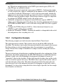
Chapter 1
General System Setup (Software Considerations)
1.1
Software considerations..................................................................................................................................................11
1.1.1
Overview............................................................................................................................................................11
1.1.2
Code execution...................................................................................................................................................11
1.1.3
Reset and booting...............................................................................................................................................11
1.1.4
1.1.3.1
Device state during reset....................................................................................................................12
1.1.3.2
Device state after reset.......................................................................................................................12
Typical system initialization .............................................................................................................................12
1.1.4.1
Lowest level assembly routines.........................................................................................................12
1.1.4.1.1 Initialize general purpose registers...................................................................................12
1.1.4.1.1.1 Unmask interrupts at ARM core ..................................................................13
1.1.4.1.1.2 Branch to start of C initialization code.........................................................13
1.1.4.2
Startup routines..................................................................................................................................13
1.1.4.2.1 Disable watchdog..............................................................................................................13
1.1.4.2.2 Initialize RAM..................................................................................................................13
1.1.4.2.3 Enable port clocks.............................................................................................................13
1.1.4.2.4 Ramp system clock to selected frequency........................................................................13
1.1.4.2.5 Enable pin interrupt...........................................................................................................14
1.1.4.2.6 Enable UART for terminal communication......................................................................14
1.1.4.2.7 Jump to start of main function for application..................................................................14
Chapter 2
General System Setup (Hardware Considerations)
2.1
Hardware considerations.................................................................................................................................................15
2.1.1
Overview............................................................................................................................................................15
2.1.2
Floorplan............................................................................................................................................................15
2.1.2.1
Connectors.........................................................................................................................................16
Kinetis L Peripheral Module Quick Reference, Rev. 0, 09/2012
Freescale Semiconductor, Inc.
3
Section number
2.1.3
Title
Page
PCB routing considerations...............................................................................................................................16
2.1.3.1
Power supply routing.........................................................................................................................16
2.1.3.2
Power supply decoupling and filtering..............................................................................................17
2.1.3.3
Oscillators..........................................................................................................................................18
2.1.3.3.1 MCG oscillator..................................................................................................................18
2.1.3.4
General filtering.................................................................................................................................23
2.1.3.4.1 RESET_b and NMI_b.......................................................................................................23
2.1.3.4.2 General purpose I/O..........................................................................................................23
2.1.3.4.3 Analog inputs....................................................................................................................23
2.1.4
PCB layer stack-up.............................................................................................................................................24
2.1.5
Other module hardware considerations..............................................................................................................26
2.1.5.1
Debug interface..................................................................................................................................26
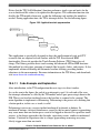
Chapter 3
Nested Vector Interrupt Controller (NVIC)
3.1
NVIC...............................................................................................................................................................................29
3.1.1
3.1.2
Overview............................................................................................................................................................29
3.1.1.1
Introduction .......................................................................................................................................29
3.1.1.2
Features .............................................................................................................................................29
Configuration examples.....................................................................................................................................30
3.1.2.1
Configuring the NVIC.......................................................................................................................30
3.1.2.1.1 Code example and explanation.........................................................................................30
3.1.2.2
Relocating the vector table.................................................................................................................32
3.1.2.2.1 Code example and explanation.........................................................................................32
Chapter 4
Clocking System
4.1
Clocking..........................................................................................................................................................................33
4.1.1
Overview............................................................................................................................................................33
4.1.2
Features..............................................................................................................................................................33
Kinetis L Peripheral Module Quick Reference, Rev. 0, 09/2012
4
Freescale Semiconductor, Inc.
Section number
4.1.3
Page
Configuration examples.....................................................................................................................................35
4.1.3.1
4.1.4
Title
Configuring the RTC clock source....................................................................................................37
Additional clock options....................................................................................................................................38
4.1.4.1
Compute operation.............................................................................................................................39
4.1.4.2
Partial stop..........................................................................................................................................39
4.1.5
Clocking system device hardware implementation...........................................................................................40
4.1.6
Layout guidelines for general routing and placement........................................................................................40
4.1.7
References..........................................................................................................................................................41
Chapter 5
Power Management Control (PMC/SMC/LLWU/RCM)
5.1
Introduction.....................................................................................................................................................................43
5.2
Using the power management controller........................................................................................................................43
5.3
5.2.1
Overview............................................................................................................................................................43
5.2.2
Using the low voltage detection system.............................................................................................................43
5.2.2.1
POR and LVD features......................................................................................................................43
5.2.2.2
Configuration examples.....................................................................................................................44
5.2.2.3
Interrupt code example and explanation............................................................................................45
5.2.2.4
Hardware implementation..................................................................................................................46
Using the system mode controller...................................................................................................................................48
5.3.1
5.3.2
Overview............................................................................................................................................................48
5.3.1.1
Introduction........................................................................................................................................48
5.3.1.2
Entering and exiting power modes.....................................................................................................49
Configuration examples.....................................................................................................................................50
5.3.2.1
SMC code example and explanation..................................................................................................50
5.3.2.2
Entering Low Leakage Stop (LLS) mode..........................................................................................51
5.3.2.2.1 Mode Entry Sequence Serialization .................................................................................51
5.3.2.3
Entering wait mode............................................................................................................................52
5.3.2.4
Exiting low-power modes..................................................................................................................52
Kinetis L Peripheral Module Quick Reference, Rev. 0, 09/2012
Freescale Semiconductor, Inc.
5
Section number
5.4
Title
Page
Using the low leakage wakeup unit................................................................................................................................53
5.4.1
5.4.2
Overview............................................................................................................................................................53
5.4.1.1
Mode transitions ................................................................................................................................53
5.4.1.2
Wake-up sources ...............................................................................................................................53
LLWU configuration examples.........................................................................................................................53
5.4.2.1
Enabling pins and modules in the LLWU..........................................................................................53
5.4.2.2
Module wake-up................................................................................................................................54
5.4.2.3
Pin wake-up........................................................................................................................................54
5.4.2.4
LLWU port and module interrupts.....................................................................................................55
5.4.2.5
Wake-up sequence.............................................................................................................................55
5.5
Module operation in low-power modes..........................................................................................................................57
5.6
Mode transition requirements.........................................................................................................................................59
5.7
Source of wake-up, pins, and modules...........................................................................................................................61
Chapter 6
IOPORT module (Single Cycle I/O Port)
6.1
Using the single cycle IOPORT module.........................................................................................................................63
6.1.1
Overview............................................................................................................................................................63
6.1.1.1
6.1.2
Mapping the IOPORT to GPIO registers...........................................................................................................63
6.1.2.1
6.2
Introduction........................................................................................................................................63
IOPORT module registers..................................................................................................................63
Sample code using the IOPORT in any run mode..........................................................................................................64
6.2.1
IOPORT code example......................................................................................................................................64
Chapter 7
Direct Memory Access (DMA) Controller
7.1
DMA...............................................................................................................................................................................67
7.1.1
Overview............................................................................................................................................................67
7.1.1.1
7.1.2
Introduction .......................................................................................................................................67
DMA trigger.......................................................................................................................................................69
7.1.2.1
Trigger mode......................................................................................................................................69
Kinetis L Peripheral Module Quick Reference, Rev. 0, 09/2012
6
Freescale Semiconductor, Inc.
Section number
Title
Page
7.1.3
DMA multiplexer...............................................................................................................................................70
7.1.4
Transfer process.................................................................................................................................................71
7.1.4.1
Multiple transfer requests...................................................................................................................72
7.1.4.2
Asynchronous transfers......................................................................................................................73
7.1.5
Configuration steps ...........................................................................................................................................73
7.1.6
Example—UART-gated DMA requests ...........................................................................................................73
7.1.6.1
Requirements.....................................................................................................................................74
7.1.6.2
Module configuration.........................................................................................................................74
Chapter 8
Universal asynchronous receiver/transmitter (UART)
8.1
Overview.........................................................................................................................................................................77
8.2
Introduction.....................................................................................................................................................................77
8.3
Features...........................................................................................................................................................................77
8.4
8.3.1
UART clock.......................................................................................................................................................78
8.3.2
UART baud rate generation...............................................................................................................................78
8.3.3
Receiver wake-up feature...................................................................................................................................79
8.3.4
Additional features.............................................................................................................................................80
Configuration examples..................................................................................................................................................84
8.4.1
Example 1: Polling/Interrupt mode of UART....................................................................................................84
8.4.2
Example 2: Functionality of UART0 in VLPS mode........................................................................................87
Chapter 9
Universal Serial Bus OTG Module
9.1
Introduction.....................................................................................................................................................................91
9.2
Features...........................................................................................................................................................................91
9.3
USB operation modes.....................................................................................................................................................91
9.4
Voltage regulator operation modes.................................................................................................................................92
9.5
Module configuration......................................................................................................................................................94
9.5.1
Module dependencies.........................................................................................................................................94
9.5.2
USB initialization process..................................................................................................................................94
Kinetis L Peripheral Module Quick Reference, Rev. 0, 09/2012
Freescale Semiconductor, Inc.
7
Section number
9.5.3
9.6
9.7
Title
Page
Voltage regulator initialization..........................................................................................................................96
Hardware implementation...............................................................................................................................................96
9.6.1
Connection diagram...........................................................................................................................................96
9.6.2
Components and placement suggestions............................................................................................................98
9.6.3
Layout recommendations...................................................................................................................................99
Example code..................................................................................................................................................................100
9.7.1
Device code........................................................................................................................................................100
9.7.2
Host code............................................................................................................................................................101
Chapter 10
Touch Sense Input (TSI) Module
10.1 Overview.........................................................................................................................................................................105
10.2 Introduction.....................................................................................................................................................................105
10.3 Features...........................................................................................................................................................................107
10.4 TSI configuration............................................................................................................................................................108
10.4.1 Configuration Example......................................................................................................................................110
10.4.1.1 Code Example and Explanation.........................................................................................................111
10.5 TSI hardware implementation.........................................................................................................................................112
10.5.1 PCB Routing and Placement..............................................................................................................................113
Chapter 11
Using Low-Power Timer (LPTMR) to Schedule Analog-to-Digital Converter (ADC) Conversion
11.1 Overview.........................................................................................................................................................................115
11.1.1 Introduction........................................................................................................................................................115
11.1.2 Features..............................................................................................................................................................116
11.2 Configuration example....................................................................................................................................................117
11.2.1 LPTMR-triggered single-ended ADC conversion.............................................................................................117
11.2.1.1 Turn on ADC and LPTMR clock gate...............................................................................................118
11.2.1.2 Configure SIM for ADC trigger.........................................................................................................118
11.2.1.3 Configure the LPTMR ......................................................................................................................118
11.2.1.4 Determine the ADC configuration.....................................................................................................118
Kinetis L Peripheral Module Quick Reference, Rev. 0, 09/2012
8
Freescale Semiconductor, Inc.
Section number
Title
Page
11.2.1.5 Using the ADC driver........................................................................................................................119
11.2.1.6 Calibrate the ADC..............................................................................................................................119
11.2.1.7 Enable the LPTMR and ADC interrupt.............................................................................................119
11.2.1.8 Start the LPTMR timer counting.......................................................................................................120
11.2.1.9 Handling LPTMR and ADC interrupt...............................................................................................120
11.2.2 ADC device hardware implementation..............................................................................................................120
11.2.3 LPTMR device hardware implementation.........................................................................................................120
11.3 PCB design recommendations........................................................................................................................................121
11.3.1 Layout guidelines...............................................................................................................................................121
11.3.1.1 General routing and placement..........................................................................................................121
11.3.2 ESD/EMI considerations ...................................................................................................................................121
Chapter 12
Timer/PWM Module (TPM)
12.1 Overview.........................................................................................................................................................................123
12.2 Introduction.....................................................................................................................................................................123
12.3 Features...........................................................................................................................................................................123
12.3.1 TPM clock..........................................................................................................................................................124
12.3.2 Interrupts and DMA...........................................................................................................................................124
12.3.3 Modes of operation............................................................................................................................................124
12.3.4 Initialization of TPM..........................................................................................................................................125
12.3.5 Updating MOD and CnV...................................................................................................................................125
12.3.6 TPM period........................................................................................................................................................125
12.3.7 TPM triggers......................................................................................................................................................126
12.3.8 Additional features.............................................................................................................................................126
12.4 Configuration examples..................................................................................................................................................127
12.4.1 Example 1 – Edge Aligned PWM and Input Capture Mode..............................................................................127
12.4.2 Example 2 – TPM functionality in low power stop mode.................................................................................131
Kinetis L Peripheral Module Quick Reference, Rev. 0, 09/2012
Freescale Semiconductor, Inc.
9
Kinetis L Peripheral Module Quick Reference, Rev. 0, 09/2012
10
Freescale Semiconductor, Inc.
Chapter 1
General System Setup (Software Considerations)
1.1 Software considerations
1.1.1 Overview
This chapter provides a quick look at some of the general characteristics of the Kinetis L
series of MCUs. This is a brief introduction of the operation of the devices and typical
software initialization.
For more information, see the device-specific reference manual and data sheet.
1.1.2 Code execution
The Kinetis L series features embedded Flash and SRAM memory for data storage and
program execution.
1.1.3 Reset and booting
When the processor exits reset, it fetches the initial stack pointer (SP) from vector table
offset 0 and the program counter (PC) from vector table offset 4. The initial vector table
must be located in the flash memory at the base address (0x0000_0000). However, the
vector table can be relocated to SRAM after the boot-up sequence if desired. This device
supports booting from internal flash and RAM. This device supports booting from
internal flash with the reset vectors located at addresses 0x0 (initial SP_main), 0x4 (initial
PC), and RAM with the relocation of the exception vector table to RAM.
After fetching the stack pointer and program counter, the processor branches to the PC
address and begins executing instructions.
Kinetis L Peripheral Module Quick Reference, Rev. 0, 09/2012
Freescale Semiconductor, Inc.
11
Software considerations
For more information, see the "Reset and Boot" chapter of the device-specific reference
manual.
1.1.3.1 Device state during reset
With the exception of the SWD pins, during reset the digital I/O pins go to a disabled
(high impedance) state with internal pullups/pulldowns disabled. Pins with analog
functionality will default to their analog functions.
1.1.3.2 Device state after reset
After reset, the digital I/O pins remain disabled until enabled by software. Also, interrupts
are disabled and the clocks to most of the modules are off. The default clock mode after
reset is FLL Engaged Internal (FEI) mode. In this mode, the system is clocked by the
frequency-locked loop (FLL) using the slow internal reference clock as its reference. The
watchdog timer is active; therefore it will need to be serviced, or disabled if debugging.
The core clock, system clock, and flash clock are enabled after reset to support booting.
Also, the flash memory controller cache and prefetch buffers are enabled.
1.1.4 Typical system initialization
The following is a summary of typical software initialization. The code snippets are taken
from a "hello_world" project written in IAR Embedded Workbench. This project is
available in the Kinetis sample code found in the file KL25_SC.exe which accompanies
this guide.
1.1.4.1 Lowest level assembly routines
These routines are assembly source code found in the file crt0.s. The address of the start
of this code is placed in the vector table offset 4 (initial program counter) so that it is
executed first when the processor starts up. This is accomplished by labeling this section,
exporting the label, and placing the label in the vector table. The vector table can be
found in vectors.h. In this example the label used is __startup.
1.1.4.1.1
Initialize general purpose registers
As a general rule, it is recommended to initialize the processor general purpose registers
(R0-R7) to zero. One way of doing this is with the LDR instruction.
Kinetis L Peripheral Module Quick Reference, Rev. 0, 09/2012
12
Freescale Semiconductor, Inc.
Chapter 1 General System Setup (Software Considerations)
LDR
LDR
LDR
LDR
LDR
LDR
LDR
LDR
1.1.4.1.1.1
CPSIE
r0,=0
r1,=0
r2,=0
r3,=0
r4,=0
r5,=0
r6,=0
r7,=0
Unmask interrupts at ARM core
i
1.1.4.1.1.2
import start
BL
; Initialize the GPRs
; Unmask interrupts
Branch to start of C initialization code
start
; call the C code
1.1.4.2 Startup routines
These routines are C source code found in the files start.c and sysinit.c. This code
provides general system initialization that may be adapted depending on the application.
1.1.4.2.1
Disable watchdog
For code development and debugging, it is best to disable the watchdog. The COP can be
disabled by clearing COPCTRL[COPT] in the SIM.
/* Disable the watchdog timer */
SIM_COPC = 0x00;
1.1.4.2.2
Initialize RAM
Depending on the application, the following steps may be required. First, copy the vector
table from flash to RAM, copy initialized data from flash to RAM, clear the zeroinitialized data section, and copy functions from flash to RAM.
1.1.4.2.3
Enable port clocks
To configure the I/O pin muxing options, the port clocks must first be enabled. This
allows the pin functions to later be changed to the desired function for the application.
SIM_SCGC5 |= (SIM_SCGC5_PORTA_MASK
| SIM_SCGC5_PORTB_MASK
| SIM_SCGC5_PORTC_MASK
| SIM_SCGC5_PORTD_MASK
| SIM_SCGC5_PORTE_MASK );
Kinetis L Peripheral Module Quick Reference, Rev. 0, 09/2012
Freescale Semiconductor, Inc.
13
Software considerations
1.1.4.2.4
Ramp system clock to selected frequency
The Multipurpose clock generator (MCG) provides several options for clocking the
system. Configure the MCG mode, reference source, and selected frequency output based
on the needs of the system.
1.1.4.2.5
Enable pin interrupt
In this example, pin PTA4 is connected to a push button. An interrupt is generated when
the button is pressed. A GPIO interrupt is used instead of an NMI interrupt because an
edge-sensitive interrupt is preferred versus a level-sensitive interrupt. This ensures that
one interrupt will occur per button press.
Interrupts need to be enabled in the ARM core, as described in the sections detailing
NVIC.
/* Configure the PTA4 pin for its GPIO function */
PORTA_PCR4 = PORT_PCR_MUX(0x1); // GPIO is alt1 function for this pin
/* Configure the PTA4 pin for rising edge interrupts */
PORTA_PCR4 |= PORT_PCR_IRQC(0x9);
/* Initialize the NVIC to enable the specified IRQ */
enable_irq(30);
NOTE
To save space, the enable_irq() function is not shown. See the
interrupts section for details on how to enable the IRQ. Also, to
save space, the interrupt service routine is not shown.
1.1.4.2.6
Enable UART for terminal communication
See the section describing UART in this document for more information.
1.1.4.2.7
Jump to start of main function for application
/* Jump to main process */
main();
Kinetis L Peripheral Module Quick Reference, Rev. 0, 09/2012
14
Freescale Semiconductor, Inc.
Chapter 2
General System Setup (Hardware Considerations)
2.1 Hardware considerations
2.1.1 Overview
This chapter will outline the best practices for hardware design when using the Kinetis L
series MCUs. The designer must consider numerous aspects when creating the system so
that performance, cost, and quality meet the end-user expectations. Performance usually
implies high speed digital signalling, but it also applies to accurate sampling of analog
signals. Cost is influenced by component selection, of which the PCB may be the most
expensive element. Quality involves manufacturability, reliability, and conformance to
industry or governmental standards.
Evaluation boards are great for evaluating the operation and performance of the many
features of Freescale MCUs. However, evaluation systems are not ideal examples for
implementation of robust system design techniques. This document will mention some of
the hardware techniques found on the Freescale Tower Systems, and will give
recommendations that are more appropriate to conventional systems that are not required
to implement all of the feature options.
2.1.2 Floorplan
The organization of the printed circuit board (PCB) depends on many factors. Typically,
there are connectors, mechanical components, high speed signals, low speed signals,
switches, and power domains, among others, that need to be considered. While placement
of connectors and some mechanical components (switches, relays, and so on) is critical to
the end product’s form, there are some basic recommendations that can significantly
affect the electrical performance and electromagnetic compatibility (EMC) of the PCB
assembly.
Kinetis L Peripheral Module Quick Reference, Rev. 0, 09/2012
Freescale Semiconductor, Inc.
15
Hardware considerations
2.1.2.1 Connectors
The PCB should be organized so that all of the connectors are along one edge of the
board and away from the MCU. The concept here is to prevent placing the MCU in
between connectors that can become effective radiators when cables are attached. This
also keeps the MCU from being in the path of high energy transients that can shoot across
the board from one connector to another. Connectors may be placed on adjacent edges of
the PCB if necessary, but only when the MCU is not in a direct path between the
connectors.
Connector locations should allow for placement of filter components. Noise must be
suppressed at the connector, before it can propagate onto the PCB. For more information
on this topic, see the input filtering section.
2.1.3 PCB routing considerations
This section covers critical power and filtering aspects of PCB layout.
2.1.3.1 Power supply routing
Routing of power and ground to digital systems is a topic that is discussed and debated in
many textbooks and references. The basic concept is to ensure that the MCU and other
digital components have a low impedance path to the power supply. The typical guidance
that was given for one and two layer PCBs was to use wide traces and few layer
transitions. The recommendations for today’s high speed MCUs follow those given for
high speed microprocessor systems – specifically, use planes for power and ground. This
may raise the PCB cost, but the benefits of crosstalk reduction, reduction of RF
emissions, and improved transient immunity can be realized with lower overall
production and maintenance costs.
In general, the ground routing should take precedence over any other routing. Ground
planes or traces should never be broken by signals. For packages with leads, like the
LQFP, a ground plane directly below the MCU package is recommended to reduce RF
emissions and improve transient immunity. All of the VSS pins of the MCU should be
tied to a ground plane. Ground traces from a plane should be kept as short as possible as
they are routed to circuitry on signal layers (top and bottom). Power planes may be
broken to supply different voltages. All of the VDD pins of the MCU should be tied to
Kinetis L Peripheral Module Quick Reference, Rev. 0, 09/2012
16
Freescale Semiconductor, Inc.
Chapter 2 General System Setup (Hardware Considerations)
the proper power plane. Power traces from the planes should be kept as short as possible
as they are routed to circuitry, such as pullups, filters, other logic and drivers, on the top
and bottom layers. More information is given in the PCB layer stack-up section below.
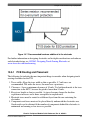
2.1.3.2 Power supply decoupling and filtering
Bypass capacitors, while also called decoupling capacitors, are the storage elements that
provide the instantaneous energy demanded by the high speed digital circuits.
Power supply bypass capacitors must be placed close to the MCU supply pins. The basic
concept is that the bypass capacitor provides the instantaneous current for every logic
transition within the MCU. Fortunately, each Kinetis MCU has a low voltage internal
regulator for the MCU core logic, therefore the abrupt current demands of the internal
high speed logic are not as critical. However, external signals demand energy from the
power rails when they transition from one logic level to the other. The bypass capacitors
provide the local filtering so that the effects of the external pin transitions are not
reflected back to the power supply, which causes RF emissions.
The basic rule of placing bypass capacitors as close as possible to the MCU is still
appropriate. The idea is to minimize the loop created by the capacitor between the VDD
and VSS pins. The implementation of this rule depends on the number of mounting
layers, how the supplies are routed, and the physical size of the capacitors:
• Number of mounting layers – PCBs with components mounted only on the top side
will have a significant limitation on how close the bypass caps can be located due to
the number of components that require space. PCBs that have components mounted
on both sides of the PCB allow closer placement of the bypass capacitors.
• Supply routing – With the Ball Grid Array (BGA) package, all of the VDD/VSS
pairs are routed to other layers under the package. This allows easier attachment of
the VDD and VSS pins to the power and ground planes within those layers. The
bypass capacitors can be placed in the area below the MCU, with connections very
close to the power pins. See the following figure.
Kinetis L Peripheral Module Quick Reference, Rev. 0, 09/2012
Freescale Semiconductor, Inc.
17
Hardware considerations
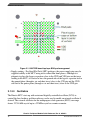
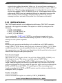
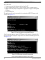
Figure 2-1. K60 TWR board top layer BGA pad arrangement
• Supply routing – For Quad Flat Pack (QFP) packages, the power supply pins may be
supplied radially to the MCU using traces rather than from planes. Although it is
adequate to place the bypass capacitors close to the VDD and VSS pins on the traces
leading to the MCU, it is better to have the ground side of the bypass capacitor tied to
the ground plane (through a via and short trace) close to the VSS pin and the VDD
side tied to the power plane (through a via and short trace) close to the VDD pin.
2.1.3.3 Oscillators
The Kinetis MCU starts up with an internal digitally controlled oscillator (DCO) to
control the bus clocking, and then software can be used to enable an external oscillator if
desired. The external oscillator for the multipurpose clock generator (MCG) can range
from a 32.768 kHz crystal up to a 32 MHz crystal or ceramic resonator.
Kinetis L Peripheral Module Quick Reference, Rev. 0, 09/2012
18
Freescale Semiconductor, Inc.
Chapter 2 General System Setup (Hardware Considerations)
2.1.3.3.1
MCG oscillator
The high speed oscillator that can be used to source the MCG module is very versatile.
The component choices for this oscillator are detailed in the device-specific reference
manual. The placement of this crystal or resonator is described here.
The EXTAL and XTAL pins are located on the outside pad ring of the BGA package and
on corner pins of the LQFP/QFN package. This allows room for placement and routing of
the crystal or resonator on the top layer, close to the MCU. The feedback resistor and
load capacitors, if needed, can be placed on the top layer as well. See Figure 2-2, Figure
2-3, and Figure 2-4.
Note that the low power modes of this oscillator do not require a feedback resistor, and
may not require external load capacitors. See the device-specific reference manual for
details. This makes it as simple as possible because only one component has to be placed
and routed. Low power oscillators are more susceptible to interference by system
generated noise, therefore the guidelines for crystal routing are important.
The crystal or resonator must be located close to the MCU. No signals of any kind should
be routed on the layer directly below the crystal. The load capacitors and ground of the
crystal package must be connected to a single ground trace coming from the closest VSS
pin or the recommended ground under the MCU. An unbroken ground plane on the layer
directly below the crystal is recommended. A ground pour must be placed around the
crystal and its load components to protect it from crosstalk from adjacent signals on the
mounting layer.
Kinetis L Peripheral Module Quick Reference, Rev. 0, 09/2012
Freescale Semiconductor, Inc.
19
Hardware considerations
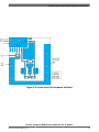
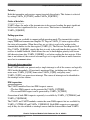
Figure 2-2. Typical crystal circuit
Kinetis L Peripheral Module Quick Reference, Rev. 0, 09/2012
20
Freescale Semiconductor, Inc.
Chapter 2 General System Setup (Hardware Considerations)
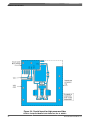
Figure 2-3. Crystal layout for low power oscillator
Kinetis L Peripheral Module Quick Reference, Rev. 0, 09/2012
Freescale Semiconductor, Inc.
21
Hardware considerations
Figure 2-4. Crystal layout for high power oscillator
Kinetis L Peripheral Module Quick Reference, Rev. 0, 09/2012
22
Freescale Semiconductor, Inc.
Chapter 2 General System Setup (Hardware Considerations)
2.1.3.4 General filtering
General purpose I/O pins should have adequate isolation and filtering from transients.
2.1.3.4.1
RESET_b and NMI_b
The RESET_b pin, if enabled, should have a 100 nF capacitor close to the MCU for
transient protection. The NMI_b pin, if enabled, must not have any capacitance
connected to it. Each pin, when enabled as their default function, has a weak internal
pullup, but an external 4.7 kΩ to 10 kΩ pullup is recommended. As with power pin
filtering, it is recommended to minimize the ground loop for the capacitor and the VDD
loop for the pullup resistor for these pins.
The RESET_b pin also has a configurable digital filter to reject potential noise on this
input after power-up. The configuration bits are located in the RCM_RPFC register.
While use of this filter may negate the need for the pullup and capacitor mentioned
above, it is still recommended to use external filtering in electrically noisy environments.
2.1.3.4.2
General purpose I/O
General purpose inputs, such as low speed inputs, timer inputs, and signals from offboard should have low pass filters (series resistor and capacitor to ground) to prevent data
corruption due to crosstalk or transients. The filter capacitor should be placed close to the
MCU pin, while the resistor can be placed closer to the source.
Inputs that come from connectors should have low pass filtering at the connector to
prevent noise from propagating onto the PCB. This requires a robust ground structure
around the connector. Series resistors for signals that come from off-board should be
placed as close to the connector as possible. A filter cap closer to the MCU input pin may
be required if the signal trace length is very long and can pick up noise from other
circuits.
Output pins must not have any significant capacitance placed close to the MCU. These
signals can have capacitors at the load or connector to minimize radiated emissions if
necessary.
2.1.3.4.3
Analog inputs
Analog inputs should also have low pass filters. The challenge with analog inputs,
especially for high resolution analog-to-digital conversions, is that the filter design needs
to consider the source impedance and sample time rather than a simple cutoff frequency.
This topic cannot be discussed in detail here, but the general concept is that fast sample
Kinetis L Peripheral Module Quick Reference, Rev. 0, 09/2012
Freescale Semiconductor, Inc.
23
Hardware considerations
times will require smaller capacitor values and source impedances than slow sample
times. Higher resolution inputs may require smaller capacitor values and source
impedances than lower resolution inputs.
In general, capacitor values can range from 10 pF for high speed conversions to 1 uF for
low speed conversions. Series resistors can range from a few hundred Ohms to 10 kΩ.
2.1.4 PCB layer stack-up
The Kinetis L series MCUs are high speed integrated circuits. Care must be taken in the
PCB design to ensure that fast signal transitions, such as rise/fall times and continuous
frequencies, do not cause RF emissions. Likewise, transient energy that enters the system
needs to be suppressed before it can affect the system operation (compatibility). The
guidance from high speed PCB designers is to have all signals routed within one
dielectric (core or prepreg) of a return path, which usually is a ground plane on a multilayer PCB and an adjacent ground on a two layer PCB. This allows return currents to
predictably flow back to the source without affecting other circuits, which is the primary
cause of radiated emissions in electronic systems. This approach requires full planes
within the PCB layer stack and partial planes (copper pours) on signal layers where
possible. All ground planes and ground pours must be connected with plenty of vias.
Likewise, all “like” power planes and power pours must be connected with plenty of vias.
Recommended layer stackups:
4-Layer PCB A:
Layer 1 (top – MCU location)—Ground plane and pads for top mounted
components, no signals
Layer 2 (inner)—Signals and power plane
Thick core
Layer 3 (inner)—Signals and power plane
Layer 4 (bottom)—Ground plane and pads for bottom mounted components, no
signals
4-Layer PCB B:
Layer 1 (top – MCU location)—Signals and poured power
Layer 2 (inner)—Ground plane
Thick core
Layer 3 (inner)—Ground plane
Layer 4 (bottom)—Signals and poured power
6-Layer PCB A:
Layer 1 (top – MCU)—Power plane and pads for top mounted components, no
signals
Kinetis L Peripheral Module Quick Reference, Rev. 0, 09/2012
24
Freescale Semiconductor, Inc.
Chapter 2 General System Setup (Hardware Considerations)
Layer 2 (inner)—Signals and ground plane
Layer 3 (inner)—Power plane
Layer 4 (inner)—Ground plane
Layer 5 (inner)—Signals and power plane
Layer 6 (bottom)—Ground plane and pads for bottom mounted components, no
signals
6-Layer PCB B:
Layer 1 (top – MCU)—Signals and power plane
Layer 2 (inner)—Ground plane
Layer 3 (inner)—Signals and power plane
Layer 4 (inner)—Ground plane
Layer 5 (inner)—Power plane
Layer 6 (bottom)—Signals and ground plane
6-Layer PCB C:
Layer 1 (top – MCU)—Signals and power plane
Layer 2 (inner)—Ground plane
Layer 3 (inner)—Signals and power plane
Layer 4 (inner)—Signals and ground plane
Layer 5 (inner)—Power plane
Layer 6 (bottom)—Signals and ground plane
8-Layer PCB A:
Layer 1 (top – MCU)—Signals
Layer 2 (inner)—Ground plane
Layer 3 (inner)—Signals
Layer 4 (inner)—Power plane
Layer 5 (inner)—Ground plane
Layer 6 (inner)—Signals
Layer 7 (inner)—Ground plane
Layer 8 (bottom)—Signals
8-Layer PCB B:
Layer 1 (top – MCU)—Signals and power plane
Layer 2 (inner)—Ground plane
Layer 3 (inner)—Signals and power plane
Layer 4 (inner)—Ground plane
Layer 5 (inner)—Power plane
Layer 6 (inner)—Signals and ground plane
Layer 7 (inner)—Power plane
Layer 8 (bottom)—Signals and ground plane
Kinetis L Peripheral Module Quick Reference, Rev. 0, 09/2012
Freescale Semiconductor, Inc.
25
Other module hardware considerations
8-Layer PCB C:
Layer 1 (top – MCU)—Signals and ground plane
Layer 2 (inner)—Power plane
Layer 3 (inner)—Ground plane
Layer 4 (inner)—Signals
Thick core
Layer 5 (inner)—Signals
Layer 6 (inner)—Ground plane
Layer 7 (inner)—Power plane
Layer 8 (bottom)—Signals and ground plane
8-Layer PCB D:
Layer 1 (top – MCU)—Signals and ground plane
Layer 2 (inner)—Power plane
Layer 3 (inner)—Ground plane
Layer 4 (inner)—Signals and power plane
Thick core
Layer 5 (inner)—Signals and power plane
Layer 6 (inner)—Ground plane
Layer 7 (inner)—Power plane
Layer 8 (bottom)—Signals and ground plane
In general, avoid placing one signal layer adjacent to another signal layer.
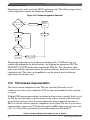
2.1.5 Other module hardware considerations
2.1.5.1 Debug interface
The Kinetis L series MCUs use the Cortex Debug interfaces for debugging and
programming. The 19-pin Cortex Debug interfaces provides connections for Serial Wire
debugging, as well as target power. The 9-pin Cortex Debug interfaces provides
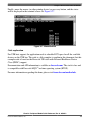
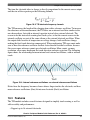
connections for Serial Wire debugging only. Figure 2-5 shows the 20-pin header
implementation with 19 pins populated. Figure 2-6 shows the 10-pin header
implementation with 9 pins populated as used on the TWR system and Freedom boards.
Kinetis L Peripheral Module Quick Reference, Rev. 0, 09/2012
26
Freescale Semiconductor, Inc.
Chapter 2 General System Setup (Hardware Considerations)
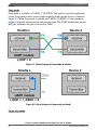
Figure 2-5. 20-pin debug interface
Kinetis L Peripheral Module Quick Reference, Rev. 0, 09/2012
Freescale Semiconductor, Inc.
27
Other module hardware considerations
Figure 2-6. 10-pin debug interface
The debug signals are multiplexed with general purpose I/O pins, therefore some signals
will require proper biasing to select the operating mode. The SWD_CLK pin has an
internal pull down device and SWD_DIO has an internal pull up device. The connectors
for this interface are keyed dual row 0.050” centered headers. When implementing either
of these headers on a target system, pin 7 must be depopulated to use the 19-pin or 9-pin
adapters from the debug tool. The Samtec part numbers for these connectors are:
•
•
•
•
FTSH-110-01-L-DV-K – 20-pin keyed connector
FTSH-105-01-L-DV-K – 10-pin keyed connector
FTSH-110-01-L-DV – 20-pin connector, no key
FTSH-105-01-L-DV – 10-pin connector, no key
This interface is useful during the development phase of a project. The header may not
need to be populated in the production phase of the project, but the PCB pads should be
kept available for future debugging purposes.
Kinetis L Peripheral Module Quick Reference, Rev. 0, 09/2012
28
Freescale Semiconductor, Inc.
Chapter 3
Nested Vector Interrupt Controller (NVIC)
3.1 NVIC
3.1.1 Overview
This chapter shows how the NVIC is integrated into the Kinetis MCUs and how to
configure it and set-up module interrupts. It also demonstrates the steps to set the
interrupts for the desired peripheral and how to locate the vector table from flash to
RAM.
3.1.1.1 Introduction
The NVIC is a standard module on the ARM Cortex M series. This module is closely
integrated with the core and provides very low latency entering and exiting an interrupt
service routine (ISR). It takes 15 cycles to exit an ISR, unless the exit from the interrupt
is into another pending ISR. In this case, the MCU tail-chains and the exit and re-entry
takes 11 cycles.
The NVIC provides four different interrupt priorities which can be used to control the
order in which interrupts must be serviced. Priorities are 0-3, with 0 receiving the highest
priority. For example, in a motor-control application, if a timer interrupt and UART occur
simultaneously, the timer interrupt that moves the motor is more critical than the UART
interrupt receiving a character. The timer priority must be set higher than the UART.
Kinetis L Peripheral Module Quick Reference, Rev. 0, 09/2012
Freescale Semiconductor, Inc.
29
NVIC
3.1.1.2 Features
On Kinetis L series MCUs the NVIC provides up to 48 interrupt sources including 16
that are core specific. It also implements up to four priority levels that are fully
programmable. The NVIC uses a vector table to manage the interrupts. This vector table
can be stored in either flash or RAM, depending on the application.
Table 3-1. Core exceptions
Address
Vector
IRQ
Source module
Source description
0
—
ARM core
Initial stack pointer
1
—
ARM core
Initial program Counter
2
—
ARM core
Non-maskable Interrupt (NMI)
3
—
ARM core
Hard fault
11
—
ARM core
SVCall
12
—
—
—
14
—
ARM core
Pendable request for system service
15
—
ARM core
System tick timer(SysTick)
ARM Core System Handler Vectors
0x0000_0000
3.1.2 Configuration examples
The NVIC is easy to configure, as demonstrated in the following examples. The first
example shows how to configure the NVIC for a module, using the low power timer
(LPTMR) as a base. The second example shows how to locate the vector table from the
flash to RAM.
3.1.2.1 Configuring the NVIC
Configuring the NVIC for the specific module involves writing three registers: NVIC Set
Enable Register (NVICSERx), NVIC Clear Pending Register (NVICCPRx), and NVIC
Interrupt Priority (NVICIPxx). After the NVIC is configured and the desired peripheral
has its interrupts enabled, the NVIC serves any pending request from that module by
going to the module's ISR.
3.1.2.1.1
Code example and explanation
This example shows how to set up the NVIC for a specific module, using the LPTMR.
The steps to configure the NVIC for this module are:
Kinetis L Peripheral Module Quick Reference, Rev. 0, 09/2012
30
Freescale Semiconductor, Inc.
Chapter 3 Nested Vector Interrupt Controller (NVIC)
1. Identify the vector number and the IRQ number of the module from the vector table
in the device-specific reference manual in the section Interrupt Channel
Assignments. For the LPTMR the vector is 44.
Table 3-2. LPTMR
vector
Address
Vector
IRQ
Source Module
0x0000_00A8
42
26
TSI
0x0000_00AC
43
27
MCG
0x0000_00B0
44
28
LPTMR
Source
Description
2. Determine which NVICSERx register contains the IRQ. Each NVICSERx register
contains 32 IRQs. Therefore, the NVICSER0 can enable from IRQ 0 to IRQ 31. In
this example, NVICSER0 is used, and the LPTMR IRQ is 28. The NVICCPRx uses
the same number, in this case, NVICCPR2.
3. To find out which bit to set, perform a modulo operation dividing the IRQ number by
32. This number is used to enable the interrupt on NVICSER0 and to clear the
pending interrupts from NVICCPR0.
Example:
LPTMR BIT = 28 mod 32
LPTMR BIT = 28
4. At this point, the interrupt for the LPTMR can be configured:
NVICICPR0|=(1<<28);
NVICISER0|=(1<<28);
//Clear any pending interrupts on LPTMR
//Enable interrupts from LPTMR module
5. Next, set the interrupt priority level. This is application dependent. On Kinetis LSeries MCUs there are four different priority levels. To set the priority, write to the
NVICIPxx register; the "xx" represents the IRQ number, which is NVICIP85 in this
example. Note the most significant nibble is used to set up the priority, the lower
nibble is reserved and reads as zero. The LPTMR example sets the priority to 3:
NVIC_IPR7 = 0x03;
//Set Priority 3 to the LPTMR module
6. After the NVIC registers are set up, finish the peripheral configuration that must
enable the interrupt.
7. In the ISR, clear the peripheral interrupt flag and read back the status register to
avoid re-entrance. For this example:
void vfnLPTMR_ISR (void)
{
Kinetis L Peripheral Module Quick Reference, Rev. 0, 09/2012
Freescale Semiconductor, Inc.
31
NVIC
LPTMR0_CSR|=LPTMR_CSR_TCF_MASK; //Clear LPTMR Compare flag
LPTMR0_CSR = ( LPTMR_CSR_TEN_MASK |
LPTMR_CSR_TIE_MASK |
LPTMR_CSR_TCF_MASK );
/*ISR code goes here*/
}
3.1.2.2 Relocating the vector table
Some applications need the vector table to be located in RAM. For example in an RTOS
implementation, the vector table needs to be in RAM, which allows the Kernel to install
ISRs by modifying the vector table during runtime.
The NVIC provides a simple way to reallocate the vector table. The user needs to set up
the Vector Table Offset Register (VTOR) with the address offset for the new position.
If you plan to store the vector table in RAM, you must first copy the table from the flash
to RAM. Also note that in some low power modes, a portion of the RAM will not be
powered, which can lead to a vector table corruption. In this case, locate the vector table
in the flash prior to entering a low power mode.
3.1.2.2.1 Code example and explanation
The CM0+ core adds support for a programmable Vector Table Offset Register (VTOR)
to relocate the exception vector table. This device supports booting from internal flash.
The vector table is initially in flash. If the vector table is needed in RAM, move it in this
manner:
1. Copy the entire vector table from flash to RAM. The linker command file labels are
useful in this step. Refer to the following sample code:
/*Address for VECTOR_TABLE and VECTOR_RAM come from the linker file*/
extern uint32 __VECTOR_TABLE[];
extern uint32 __VECTOR_RAM[];
/* Copy the vector table to RAM */
if (__VECTOR_RAM != __VECTOR_TABLE)
{
for (n = 0; n < 0x104; n++)
__VECTOR_RAM[n] = __VECTOR_TABLE[n];
}
2. After the table has been copied, set the proper offset for the VTOR register:
/* Point the VTOR to the new copy of the vector table */
write_vtor((uint32)__VECTOR_RAM);
It is important to follow these steps in order, to ensure that there is always a valid vector
table.
Kinetis L Peripheral Module Quick Reference, Rev. 0, 09/2012
32
Freescale Semiconductor, Inc.
Chapter 4
Clocking System
4.1 Clocking
4.1.1 Overview
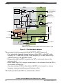
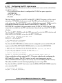
This chapter will discuss the clocking system and the multipurpose clock generator
(MCG) module. Examples will provide an overview of how to switch between the MCG
modes and specifically how to enable the on-chip PLL for high-speed operation. Clock
selection options will be discussed for the RTC.
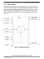
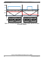
4.1.2 Features
An example of the clocking system is summarized in the following figure. Not all clock
sources will be available on specific devices. Refer to the individual device reference
manual for full details of the available clock sources.
Kinetis L Peripheral Module Quick Reference, Rev. 0, 09/2012
Freescale Semiconductor, Inc.
33
Clocking
SIM
MCG
4 MHz IRC
FCRDIV
MCGIRCLK
CG
32 kHz IRC
FLL
Clock options for
some peripherals
(see note)
OUTDIV1
CG
Core clock,
platform clock,
and system clock
OUTDIV4
CG
Bus clock/
Flash clock
MCGOUTCLK
MCGFLLCLK
FRDIV
MCGPLLCLK
MCGPLLCLK/
MCGFLLCLK
÷2
System oscillator
EXTAL0
OSCCLK
XTAL_CLK
XTAL0
OSC
logic
OSCERCLK
CG
ERCLK32K
OSC32KCLK
RTC_CLKIN
Clock options for some
peripherals (see note)
PLL
PMC
PMC logic
Counter logic
LPO
RTC_CLKOUT
1Hz
RTC
CG — Clock gate
Note: See subsequent sections for details on where these clocks are used.
Figure 4-1. Clock distribution diagram
The system level clocks are provided by the MCG. The MCG consists of:
• Two individually trimmable internal reference clocks (IRC), a slow IRC with a
frequency of ~32 kHz and a fast IRC with a frequency of ~4 MHz, which can be
reduced by means of the FCRDIV divider
• Frequency locked loop (FLL) using the slow IRC or an external source as the
reference clock
• Phase locked loop (PLL) using an external source as the reference clock (the PLL is
not available on all devices
• Auto trim machine (ATM) to allow both of the IRCs to be trimmed to a custom
frequency using an externally-generated reference clock
The clocks provided by the MCG are summarized as follows:
Kinetis L Peripheral Module Quick Reference, Rev. 0, 09/2012
34
Freescale Semiconductor, Inc.
Chapter 4 Clocking System
• MCGOUTCLK – The main system clock used to generate the core, bus, and memory
clocks. It can be generated from one of the on-chip reference oscillators, the on-chip
crystal/resonator oscillator, an externally generated square wave clock, the FLL, or
the PLL.
• MCGFLLCLK – The output of the FLL and is available any time the FLL is enabled.
• MCGPLLCLK – The output of the PLL and is available any time the PLL is enabled.
• MCGIRCLK – The output of the selected IRC. The selected IRC will be enabled
whenever this clock is selected.
In addition to the clocks provided by the MCG, there are three other system level clock
sources available for use by various peripheral modules:
• OSCERCLK – The clock provided by the system oscillator and is the output of the
oscillator or the external square wave clock source.
• ERCLK32K – The output of the system oscillator if it is configured in low power
mode at 32 kHz, the external RTC_CLKIN path or the low power oscillator (LPO).
• LPO – The output of the low power oscillator. It is an on-chip, very low power
oscillator with an output of approximately 1 kHz that is available in all run and low
power modes except VLLS0.
4.1.3 Configuration examples
The MCG can be configured in one of several modes to provide a flexible means of
providing clocks to the system for a wide range of applications.
After exiting reset, or recovering from a very low leakage state, the MCG will be in FLL
engaged internal (FEI) mode with MCGCLKOUT at 20.97 MHz, assuming a factory
trimmed slow IRC frequency of 32.768 kHz. If a different MCG mode is required, the
MCG can be transitioned to that mode under software control.
It is only possible to transition directly to certain MCG modes. Refer to the individual
device reference manual for details on this. It may be required to transition through
several modes to reach the desired MCG mode. When transitioning from one clock mode
to another, you must ensure that you have fully entered that mode before moving to the
next mode. The mcg.c file within the sample code contains examples of how to perform
all the individual clock mode transitions. The pll_init function combines three of these
individual transitions into one function. The specific MCG register operations will be
discussed below.
In this example, the PLL will be configured to use an external 8 MHz clock from the
crystal oscillator and generate a 96 MHz output frequency. This is a typical configuration
when the USB module is being used. The MCGPLLCLK frequency is half the PLL
Kinetis L Peripheral Module Quick Reference, Rev. 0, 09/2012
Freescale Semiconductor, Inc.
35
Clocking
frequency. When it is desired to provide the USB clock of 48 MHz, the PLL must be set
at 96 MHz. The MCG is configured to minimize PLL jitter, that is,maximum PLL
frequency with the minimum multiplication factor.
The first step is to move from the default FEI mode to the FLL bypassed external mode
(FBE).
//
//
//
//
first configure the oscillator settings in the MCG_C2 register
the RANGE value is determined by the external frequency. Since the RANGE
parameter affects the FRDIV divide value it still needs to be set correctly even
if an external clock is being used
MCG_C2 = (MCG_C2_RANGE0(1) | MCG_C2_EREFS0_MASK);
//
//
//
//
//
The FRDIV is determined by the reference clock frequency and should be set to
keep the FLL ref clock frequency within the correct range. For 8MHz ref this
needs to be a divide of 256
The CLKS bits must be set to b'10 to select the external reference clock
Clearing IREFS selects and enables the external oscillator
MCG_C1 = (MCG_C1_CLKS(2) | MCG_C1_FRDIV(3));
// When the external oscillator is used need to wait for OSCINIT to set
for (i = 0 ; i < 20000 ; i++)
{
// jump out early if OSCINIT sets before loop finishes
if (MCG_S & MCG_S_OSCINIT0_MASK) break;
}
// wait for Reference clock Status bit to clear
for (i = 0 ; i < 2000 ; i++)
{
// jump out early if IREFST clears before loop finishes
if (!(MCG_S & MCG_S_IREFST_MASK)) break;
}
// Wait for clock status bits to show clock source is ext ref clk
for (i = 0 ; i < 2000 ; i++)
{
// jump out early if CLKST shows EXT CLK selected before loop finishes
if (((MCG_S & MCG_S_CLKST_MASK) >> MCG_S_CLKST_SHIFT) == 0x2) break;
}
// Now in FBE
After making changes to clock selection bits or enabling either the oscillator of PLL, the
appropriate status bits must be verified before continuing. A simple "while" loop is not
recommended for polling the status bits. If for some reason the bit being checked does
not update, the “while" loop will never exit, unless a timeout mechanism is used. A "for"
loop is used here to perform this function. If a timeout is generated, a decision can be
made about what to do depending on the status bits that failed to update. For example, if
the oscillator does not start due to a damaged PCB trace, the decision to continue with an
internal-only clocking mode can be made with an appropriate indication to the user or a
central monitoring station.
Kinetis L Peripheral Module Quick Reference, Rev. 0, 09/2012
36
Freescale Semiconductor, Inc.
Chapter 4 Clocking System
When an external clock is being used, it is recommended to enable the clock monitor.
This can be configured to generate an interrupt or a system reset. This is performed by
the statement:
MCG_C6 |= MCG_C6_CME0_MASK;
The next step is to enable the PLL, and move to PLL bypassed external mode. This
allows the PLL to lock while still clocking the system from the external reference clock.
// Configure MCG_C5 to set the PLL reference clock at the right frequency
MCG_C5 |= MCG_C5_PRDIV0(1);
//set PLL ref divider to divide by 2
// Configure MCG_C6 to set the PLL multiplier and enable the PLL
// The PLLS bit is set to enable the PLL, MCGOUT still sourced from ext ref clk
temp_reg
temp_reg
temp_reg
MCG_C6 =
= MCG_C6; // store present C6 value (as CME0 bit was previously set)
&= ~MCG_C6_VDIV0_MASK; // clear VDIV settings
|= MCG_C6_PLLS_MASK | MCG_C6_VDIV0(0); // write new VDIV and enable PLL
temp_reg; // update MCG_C6
// wait for PLLST status bit to set
for (i = 0 ; i < 2000 ; i++)
{
// jump out early if PLLST sets before loop finishes
if (MCG_S & MCG_S_PLLST_MASK) break;
}
// Wait for LOCK bit to set
for (i = 0 ; i < 4000 ; i++)
{
// jump out early if LOCK sets before loop finishes
if (MCG_S & MCG_S_LOCK0_MASK) break;
}
// now in PBE
After the PLL is enabled and locked, the MCGOUTCLK can be switched to the PLL
output. Before switching to this higher frequency clock you must set the system clock
dividers to keep the system clock frequencies within specifications.
// set the core clock divider to divide by 2
// set the bus clock divider to divide by 2 (bus clock is sourced from core clock)
SIM_CLKDIV1 = (SIM_CLKDIV1_OUTDIV1(1) | SIM_CLKDIV1_OUTDIV4(1) );
Now it is possible to switch to the PLL.
// clear CLKS to switch CLKS mux to select the PLL as MCGCLKOUT
MCG_C1 &= ~MCG_C1_CLKS_MASK;
// Wait for clock status bits to update
for (i = 0 ; i < 2000 ; i++)
{
// jump out early if CLKST = 3 before loop finishes
if (((MCG_S & MCG_S_CLKST_MASK) >> MCG_S_CLKST_SHIFT) == 0x3) break;
}
// Now in PEE
Kinetis L Peripheral Module Quick Reference, Rev. 0, 09/2012
Freescale Semiconductor, Inc.
37
Clocking
4.1.3.1 Configuring the RTC clock source
The RTC does not have a dedicated oscillator, but the clock source can be selected from
one of three options:
• The system oscillator when it is configured for 32 kHz, low power operation
(OSC32KCLK)
• The RTC_CLKIN pin
• The LPO
The time keeping function of the RTC and the RTC_CLKOUT frequency will be correct
only when a 32.768 kHz clock source is used. The LPO can be used only for a timed
wake up function. The OSC32KCLK is only available when an external 32 kHz crystal is
used and the oscillator low power mode is selected (MCG_C2[HGO0] = 0). The
OSC32KCLK is available in all power modes except VLLS0. In VLLS0, the only clock
source that is available for the RTC, and therefore a timed wake up, is the RTC_CLKIN
selection.
To select the RTC_CLKIN in path, the GPIO mux must be set to the GPIO selection and
SIM_SOPT1[OSC32KSEL] set to select the RTC_CLKIN path.
// Ensure PTC1 is configured as RTC input clock
PORTC_PCR1 = ~PORT_PCR_MUX_MASK ;
PORTC_PCR1 = PORT_PCR_MUX(1) ;
// RTC_CLKIN selected as the ERCLK32K
SIM_SOPT1 |= SIM_SOPT1_OSC32KSEL(2);
To select the OSC32KCLK the oscillator must be configured by means of the RTC_CR
register and the SIM_SOPT1[OSC32KSEL] field set to select the OSC32KCLK.
// Enable the oscillator by means of the RTC_CR register
// Note that if it is desired to use the the internal load capacitors, they MUST be
// selected in the same register using the SCxP bits
OSC_CR |= OSC_CR_OSCE_MASK; // set the oscillator enable bit
// Oscillator selected as the ERCLK32K
SIM_SOPT1 &= ~SIM_SOPT1_OSC32KSEL_MASK; // Clear the OSC32KSEL field to select osc
Always enable the oscillator using the RTC_CR register rather than by configuring the
MCG and OSC registers. The RTC registers are only reset during power on reset,
whereas the MCG and OSC registers are reset by any reset and during VLLSx recovery.
This allows the RTC to retain time keeping during any reset except POR.
To select the LPO as the RTC clock source only the SIM_SOPT1[OSC32KSEL] must be
set to select the LPO.
// LPO selected as the ERCLK32K
SIM_SOPT1 |= SIM_SOPT1_OSC32KSEL(3);
Kinetis L Peripheral Module Quick Reference, Rev. 0, 09/2012
38
Freescale Semiconductor, Inc.
Chapter 4 Clocking System
4.1.4 Additional clock options
The Kinetis L series offers three new clock options. These allow for additional current
savings by automatically shutting down system level clocks. These options are briefly
described below. Refer to the device reference manual for further details.
4.1.4.1 Compute operation
Compute operation (CPO) is a means of reducing the the current consumption in RUN or
VLPR modes. Access to the peripherals is not possible and only the platform resources
are available, including the MCM, NVIC, IOPORT, and SysTick. CPO is intended to be
used in computationally intensive applications when peripheral access is not required.
Although the IOPORT is accessible, the GPIO input state cannot be read, but the GPIO
output state can be controlled. Any off platform peripheral access will result in a bus
error.
Asynchronous interrupts and DMA transfer requests are still available when using CPO.
A DMA request will automatically exit CPO and re-enter CPO when it has completed.
Most peripheral interrupts will require CPO to be exited before servicing them.
To enter or exit CPO simply requires that CPOREQ be set/cleared, and CPOACK be
checked that it has updated appropriately.
/* Enter compute operation */
MCM_CPO |= MCM_CPO_CPOREQ_MASK; //
while(!(MCM_CPO & MCM_CPO_CPOACK_MASK));
/* Exit compute operation */
MCM_CPO &= ~MCM_CPO_CPOREQ_MASK;
while (MCM_CPO & MCM_CPO_CPOACK_MASK);
4.1.4.2 Partial stop
There are two partial stop options: Partial Stop 1 (PSTOP1) and Partial Stop 2 (PSTOP2).
In PSTOP1, the system enters STOP mode with the core, system, and bus clocks gated
off but keeps the MCG clocks running and the PMC remains on. This allows for a faster
wakeup at the expense of higher power consumption.
In PSTOP2, only the core and system clocks are gated off, and the MCG clocks and PMC
remain on. This allows peripherals which are clocked by the bus clock to remain active.
The partial stop options are enabled by means of setting the appropriate STOP level in
the SMC_STOPCTRL register.
/* Enter normal STOP */
SMC_STOPCTRL = SMC_STOPCTRL_PSTOPO(0); // this also clears the other register bits
Kinetis L Peripheral Module Quick Reference, Rev. 0, 09/2012
Freescale Semiconductor, Inc.
39
Clocking
/* Enter PSTOP1 */
SMC_STOPCTRL = SMC_STOPCTRL_PSTOPO(1); // this also clears the other register bits
/* Enter PSTOP2 */
SMC_STOPCTRL = SMC_STOPCTRL_PSTOPO(2); // this also clears the other register bits
4.1.5 Clocking system device hardware implementation
It is possible to provide all the system level clocks from internal sources. However, if the
PLL is to be used or an accurate reference clock is required, an external clock must be
provided. This can be from an externally generated clock source that provides a square
wave clock, or it can be from an internal oscillator using an external crystal or resonator.
The main system oscillator can be configured in various ways depending on the crystal
frequency and mode being used. Refer to the device-specific reference manual for details.
When the oscillator is configured for low power, an integrated oscillator feedback resistor
is provided. The oscillator also has programmable internal load capacitors when it is
configured as a 32kHz oscillator (RANGE = 0). The internal crystal load capacitors are
selectable in software to provide up to 30 pF, in 2 pF increments, for each of the EXTAL
and XTAL pins. This provides an effective series capacitive load of up to 15 pF. The
parasitic capacitance of the PCB should also be included in the calculation of the total
crystal load. The combination of these two values will often mean that no external load
capacitors are required when using a 32 kHz crystal.
If either of the oscillator pins are not being used, they may be left unconnected in their
default reset configuration or may be used as GPIO.
4.1.6 Layout guidelines for general routing and placement
Use the following general routing and placement guidelines when laying out a new
design. These guidelines will help to minimize electromagnetic compatibility (EMC)
problems:
• To minimize parasitic elements, surface mount components must be used where
possible
• All components must be placed as close to the MCU as possible.
• If external load capacitors are required, they must use a common ground connection
shared in the center
• If the crystal, or resonator, has a ground connection, it must be connected to the
common ground of the load capacitors
• Where possible:
Kinetis L Peripheral Module Quick Reference, Rev. 0, 09/2012
40
Freescale Semiconductor, Inc.
Chapter 4 Clocking System
• Keep high-speed IO signals as far from the EXTAL and XTAL signals as
possible
• Do not route signals under oscillator components - on same the layer or layer
below
• Select the functions of pins close to EXTAL and XTAL to have minimal
switching to reduce injected noise
4.1.7 References
The following list of application notes associated with crystal oscillators are available on
the Freescale website at www.freescale.com. They discuss common oscillator
characteristics, potential problems, and troubleshooting guidelines:
•
•
•
•
AN1706: Microcontroller Oscillator Circuit Design Considerations
AN1783: Determining MCU Oscillator Start-Up Parameters
AN2606: Practical Considerations for Working With Low-Frequency Oscillators
AN3208: Crystal Oscillator Troubleshooting Guide
Kinetis L Peripheral Module Quick Reference, Rev. 0, 09/2012
Freescale Semiconductor, Inc.
41
Clocking
Kinetis L Peripheral Module Quick Reference, Rev. 0, 09/2012
42
Freescale Semiconductor, Inc.
Chapter 5
Power Management Control (PMC/SMC/LLWU/RCM)
5.1 Introduction
This chapter is a brief description of the power management features of the Kinetis L
series 32-bit MCU.
There are four modules covered in this chapter:
•
•
•
•
Power Management Controller (PMC)
System Mode Controller (SMC)
Low Leakage Wake-up Unit (LLWU)
Reset Control Module(RCM)
5.2 Using the power management controller
5.2.1 Overview
This section will demonstrate how to use the power management controller (PMC) to
protect an MCU from unexpected low VDD events. References to other protection options
will also be made.
5.2.2 Using the low voltage detection system
5.2.2.1 POR and LVD features
The POR and LVD functions allow protection of memory contents from brown out
conditions and the operation of the MCU below the specified VDD levels. As noted in
the module operation in the low power modes section, the LVD circuit is available only
Kinetis L Peripheral Module Quick Reference, Rev. 0, 09/2012
Freescale Semiconductor, Inc.
43
Using the low voltage detection system
in RUN, WAIT, and STOP modes. POR circuitry is on in all modes and can be optionally
disabled in VLLS0. The user has control over whether LVD is used and whether the POR
is enabled in the lowest power mode (VLLS0). When using the low voltage detect
features, the user has full control over the LVD and LVW trip voltages. The LVW is a
warning detect circuit and the LVD is reset detect circuit.
As voltage falls below the warning level, the LVW circuit flags the warning event and
can cause an interrupt. If the voltage continues to fall, the LVD circuit flags the detect
event and can either cause a reset or an interrupt. The user can choose what action to take
in the interrupt service routine. If a detect is selected to drive reset, the LVD circuit holds
the MCU in reset until the supply voltage rises above the detect threshold.
The POR circuit for the MCU will hold the MCU in reset based upon the VDD voltage.
Before entering the VLLS0 low power mode, the user can choose to disable the POR
circuit. Because the MCU is switched off in VLLS0, the POR protection is not really
needed and can be disabled. This saves a few hundred nano amps of power while the
MCU is in this mode.
If the POR circuit is disabled in VLLS0, the MCU will continue to hold the state of the
pins until the VDD levels are much lower than the POR trip voltage levels.
Exiting VLLS0 follows the reset mode. The POR circuit is reenabled protecting the MCU
operation during the recovery.
5.2.2.2 Configuration examples
LVD and LVW initialization code is given below: Notice the comments describing the
chosen settings. You should select the parameter options for your application. The NVIC
vector flag may be set and is cleared if interrupts are enabled. The Interrupt is enabled in
the NVIC in this initialization with the call to function enable_irq(LVD_irq_no):
/***************************************************************/
/* LVD and LVD initialzation routine.
* sets up the LVD and LVW control registers
*
* This function can be used to set up the low voltage detect
* and warning. While the device is in the very low power or low
* leakage modes, the LVD system is disabled regardless of LVDSC1
* settings. To protect systems that must have LVD always on,
* configure the SMC's power mode protection register (PMPROT)
* to disallow any very low power or low leakage modes from
* being enabled.
*
* Parameters:
* lvd_select = 0x00 Low trip point selected (V LVD = V LVDL )
*
= 0x01 High trip point selected (V LVD = V LVDH )
*
= 0x10 Reserved
*
= 0x11 Reserved
* lvd_reset_enable = 0x00 LVDF does not generate hardware resets
*
= 0x10 Force an MCU reset when LVDF = 1
* lvd_int_enable = 0x00 Hardware interrupt disabled
Kinetis L Peripheral Module Quick Reference, Rev. 0, 09/2012
44
Freescale Semiconductor, Inc.
Chapter 5 Power Management Control (PMC/SMC/LLWU/RCM)
*
= 0x20 Request a hardware interrupt if LVDF = 1
* lvw_select = 0x00 Low trip point selected (VLVW = VLVW1)
*
= 0x01 Mid 1 trip point selected (VLVW = VLVW2)
*
= 0x10 Mid 2 trip point selected (VLVW = VLVW3)
*
= 0x11 High trip point selected (VLVW = VLVW4)
* lvw_int_enable = 0x00 Hardware interrupt disabled
*
= 0x20 Request a hardware interrupt if LVWF = 1
*/
void LVD_Initalize(unsigned char lvd_select,
unsigned char lvd_reset_enable,
unsigned char lvd_int_enable,
unsigned char lvw_select,
unsigned char lvw_int_enable){
/*enable LVD Reset ? LVD Interrupt.select high or low LVD */
PMC_LVDSC1 = PMC_LVDSC1_LVDACK_MASK |
(lvd_reset_enable) |
lvd_int_enable
|
PMC_LVDSC1_LVDV(lvd_select);
/* select LVW level 1,2,3 or 4 */
PMC_LVDSC2 = PMC_LVDSC2_LVWACK_MASK |
(lvw_int_enable) |
//LVW interrupt?
PMC_LVDSC2_LVWV(lvw_select);
/* if interrupts requested
clear pending flags in NVIC and enable interrupts */
if (((PMC_LVDSC1 & PMC_LVDSC1_LVDIE_MASK)
>>PMC_LVDSC1_LVDIE_SHIFT) |
((PMC_LVDSC2 & PMC_LVDSC2_LVWIE_MASK)
>>PMC_LVDSC2_LVWIE_SHIFT))
{
enable_irq(LVD_irq_no); // ready for this interrupt.
}
}
5.2.2.3 Interrupt code example and explanation
The LVD circuitry can be programmed to cause an interrupt. You should create a service
routine to clear the flags and react appropriately. An example of such an interrupt service
routine is given.
To clear a warning or detect interrupt flag two things must happen:
1. The VDD voltage must return to a nominal voltage above the threshold.
2. A write to the LVDACK bit must be done to clear the LVDF indicator or a write to
the LVWACK bit must be done to clear the LVWF indicator.
If the ACK bit is written and the voltage does not go back above the threshold, the
interrupt flag will not clear and the interrupt routine will be reentered.
void pmc_lvd_isr(void)
{
if (PMC_LVDSC1 &PMC_LVDSC1_LVDF_MASK){
printf("[LVD_isr]LV DETECT interrupt occurred");
}
if (PMC_LVDSC2 &PMC_LVDSC2_LVWF_MASK){
printf("[LVD_isr]LV WARNING interrupt occurred");
}
Kinetis L Peripheral Module Quick Reference, Rev. 0, 09/2012
Freescale Semiconductor, Inc.
45
Using the low voltage detection system
// ack to clear initial flags
PMC_LVDSC1 |= PMC_LVDSC1_LVDACK_MASK;
PMC_LVDSC2 |= PMC_LVDSC2_LVWACK_MASK;
}
5.2.2.4 Hardware implementation
RESET PIN: The reset pin is an open drain and has an internal pullup device. The pin is
driven out if the internal circuitry detects a reset. This is true for all resets, except when
there is a recovery from the VLLSx modes.
Although the wake-up recovery from VLLSx modes is through the reset flow, the reset
pin is not driven out of the MCU. The reason for this is that I/O is held in the pre-lowpower mode entry state so the internal reset action is blocked from being driven out.
If reset is driven low for longer than minimum pulse width to pass the analog filter and
the digital filter settings, the MCU will wake from any low-power mode and the PIN bit
in the RCM_SRS0 register will be set.
The reset pin can be disabled by clearing the RESET_PIN_CFG bit in the Flash Option
Register (FOPT).
VDD: The VDD supply pins can be driven between 1.71 V and 3.6 V DC.
The following diagram shows a representative timing diagram during POR.
Figure 5-1. Representative timing diagram during POR
Kinetis L Peripheral Module Quick Reference, Rev. 0, 09/2012
46
Freescale Semiconductor, Inc.
Chapter 5 Power Management Control (PMC/SMC/LLWU/RCM)
The following diagram shows the observed behavior of the reset pin during a ramp of
VDD. In both of the following diagrams RESET asserts initially as the POR circuit is
powered up. Next RESET is released when untrimmed LVD level is reached. Next
RESET is asserted when LVD trim register is loaded, followed by RESET being released
when trimmed LVD level is reached.
Figure 5-2. Observed RESET pin behavior during normal slow VDD rise
The following diagram shows the observed behavior of the reset pin during a fast ramp of
VDD.
Figure 5-3. Observed RESET pin behavior during normal fast VDD rise
Kinetis L Peripheral Module Quick Reference, Rev. 0, 09/2012
Freescale Semiconductor, Inc.
47
Using the system mode controller
5.3 Using the system mode controller
5.3.1 Overview
This section will demonstrate how to use the system mode controller (SMC). The SMC is
responsible for controlling the entry and exit from all of the run, wait, and stop modes of
the MCU. This module works in conjunction with the RCM, PMC, and the LLWU to
wake-up the MCU and move between power modes.
5.3.1.1 Introduction
There are 10 power modes and some new clocking options. These modes and options are
described below.
1. Run — Default Operation of the MCU out of Reset, On-chip voltage regulator is On,
full capability.
2. Very Low Power Run (VLPR) — On-chip voltage regulator is in a mode that
supplies only enough power to run the MCU in a reduced frequency. Core and Bus
frequency limited to 2 MHz.
3. Wait — ARM core enters Sleep mode, NVIC remains sensitive to interrupts,
Peripherals Continue to be clocked.
4. Stop — ARM core enters DeepSleep mode, NVIC is disabled, WIC is used to wake
up from interrupt, peripheral clocks are stopped.
5. Very Low Power Wait (VLPW) — ARM core enters Sleep mode, NVIC remains
sensitive to interrupts (FCLK = ON), On-chip voltage regulator is in a mode that
supplies only enough power to run the MCU at a reduced frequency.
6. Very Low Power Stop (VLPS) — ARM core enters DeepSleep mode, NVIC is
disabled (FCLK = OFF), WIC is used to wake up from interrupt, peripheral clocks
are stopped, On-chip voltage regulator is in a mode that supplies only enough power
to run the MCU at a reduced frequency, all SRAMs are operating (content retained
and I/O states held).
7. Low Leakage Stop (LLS) — ARM core enters DeepSleep mode, NVIC is disabled,
LLWU is used to wake up, peripheral clocks are stopped, all SRAM is operating
(content retained and I/O states held), most peripherals are in state retention mode
(cannot operate).
8. Very Low Leakage Stop3 (VLLS3) — ARM core enters SleepDeep mode, NVIC is
disabled, LLWU is used to wake up, peripheral clocks are stopped, all SRAMs are
operating (content retained and I/O states held), and most modules are disabled.
Kinetis L Peripheral Module Quick Reference, Rev. 0, 09/2012
48
Freescale Semiconductor, Inc.
Chapter 5 Power Management Control (PMC/SMC/LLWU/RCM)
9. Very Low Leakage Stop 1 (VLLS1) — ARM core enters SleepDeep mode, NVIC is
disabled, LLWU is used to wake up, peripheral clocks are stopped, all SRAMs are
powered down, and I/O states held. Most modules are disabled.
10. Very Low Leakage Stop 0 (VLLS0) — Lowest Power Mode ARM core enters
SleepDeep mode, NVIC is disabled, LLWU is used to wake up, peripheral clocks are
stopped, All SRAMs are powered down, and I/O states held. Most modules are
disabled, LPO shut down, optional POR brown-out detection.
The modules available in each of the power modes are described in a table. Please see
Module operation in low-power modes for the details of the module operations in each of
the low-power modes.
The Kinetis L series introduces new clocking options. Please see Additional clock
options for the details of these new clocking options.
• Compute mode — ARM core remains enabled with full access to the SRAM, flash
and IOPORT, but places all other bus masters and peripherals into their stop mode.
Compute mode can be entered from RUN or VLPR.
• Partial Stop (PSTOP1) — ARM core enters DeepSleep mode, NVIC is disabled,
WIC is used to wake up from interrupt. When configured for PSTOP1, both the
system clock and bus clock are gated. All bus masters and bus slaves enter Stop
mode, but the clock generators in the MCG and the on-chip regulator in the PMC
remain in Run (or VLP Run) mode.
• Partial Stop (PSTOP2) — ARM core enters DeepSleep mode, NVIC is disabled,
WIC is used to wake up from interrupt. When configured for PSTOP2, only the core
and system clocks are gated and the bus clock remains active.
5.3.1.2 Entering and exiting power modes
SMC controls entry into and exit from each of the power modes. The WFI instruction
invokes wait and stop modes for the chip. The processor exits the low-power mode via an
interrupt. For LLS and VLLS modes, the wake-up sources are limited to LLWU
generated wake-ups, NMI pin, or RESET pin assertions. When the NMI pin or RESET
pin have been disabled through associated FOPT settings, then these pins are ignored as
wake-up sources. The wake-up flow from VLLSx is always through reset.
NOTE
The WFE instruction can have the side effect of entering a lowpower mode, but that is not its intended usage. See ARM
documentation for more on the WFE instruction.
Kinetis L Peripheral Module Quick Reference, Rev. 0, 09/2012
Freescale Semiconductor, Inc.
49
Using the system mode controller
On VLLS recoveries, the I/O pins continue to be held in a static state after code execution
begins, allowing software to reconfigure the system before unlocking the I/O. RAM is
retained in VLLS3 only.
5.3.2 Configuration examples
How you decide which modes to use in your solution is an exercise in matching the
requirements of your system, and selecting which modules are needed during each mode
of the operation for your application. The best way to explain would be to work through
an example.
For example, consider the case of a battery-operated human interface device that requires
a real-time clock timebase. It will wake up every second, update the time of day, and
check the conditions of several sensors. Then it will take action based upon the state and,
when requested, perform high levels of computation to control the operation of a device.
After reviewing the power modes table in Module operation in low-power modes, you
should be able to identify which of the modules are functioning in each of the low-power
modes.
At this point, notice that the RTC, the LPTMR, and optionally, the brown-out detection,
are the only modules that are fully functional in all of the lowest power modules. Notice
also the modules that allow wake-up in the low-power modes such as the GPIO, LLWU,
TSI, or the comparator.
In this example system, the MCU would spend most of the time in one of the lower
power modes waking up every second to update the time of day variables and update the
display, plus other house-keeping tasks.
The MCU could also wake up from a user input. This could be hitting a button, a touch of
a capacitive sensor, the rise or fall of an analog signal from a sensor feeding the
comparator. To enable these sources please refer to the LLWU section 3 in the devicespecific reference manual for configuration details.
The example drivers code for SMC are available from the Freescale Web site
www.freescale.com.
Please refer to AN4503 for power management ideas and explanations as well as mode
entry and exit drivers.
5.3.2.1 SMC code example and explanation
There are four registers in the system mode controller:
Kinetis L Peripheral Module Quick Reference, Rev. 0, 09/2012
50
Freescale Semiconductor, Inc.
Chapter 5 Power Management Control (PMC/SMC/LLWU/RCM)
• PMPROT: Power Management Protection
• PMCTRL:controls entry into low-power run and stop modes
• STOPCTRL: provides various control bits allowing the user to fine tune power
consumption during the stop mode
• PMSTAT: a read-only register that indicates the current power mode of the system
PMPROT is a write once register after a reset. This means that when written, all
subsequent writes are ignored. In our example system above, our two basic modes of
operation are Run mode and LLS mode. If we do not want the MCU to be in any other
low-power mode, we would want to write the ALLS bit in the PMPROT register.
SMC_PMPROT = SMC_PMPROT_ALLS_MASK;
This write allows the MCU to enter WAIT, Normal STOP or LLS only. It is then no
longer possible to enter any other low-power mode.
After the PMPROT register has been written, the write to PMCTRL and STOPCTRL
determines the mode that will be entered. For our example, entry into LLS mode would
be enabled with this write sequence.
SMC_PMCTRL &= ~SMC_PMCTRL_STOPM_MASK;
SMC_PMCTRL |= SMC_PMCTRL_STOPM(0x3);
5.3.2.2 Entering Low Leakage Stop (LLS) mode
After the previous two setup steps have been done, the low-power stop mode would be
entered with a write to the SCR register in the core control logic to set the SLEEPDEEP
bit.
SCB_SCR |= SCB_SCR_SLEEPDEEP_MASK;
When the WFI instruction is executed, the mode controller will step through the lowpower entry state machine making sure all of the modules are ready to enter the lowpower mode. If, for instance, the UART is finishing a serial transmission it would hold
off the entry into the LLS until the transmission is completed. In C, the syntax to execute
the core instruction WFI is:
asm("WFI");
This statement can be placed anywhere in the code and once executed, the MCU will
enter the selected low-power mode. It takes approximately 1 microsecond to enter the
low-power mode if there are no modules holding off the low-power mode entry (stop
mode acknowledge).
Kinetis L Peripheral Module Quick Reference, Rev. 0, 09/2012
Freescale Semiconductor, Inc.
51
Using the system mode controller
5.3.2.2.1
Mode Entry Sequence Serialization
To ensure that the correct mode is entered there are some serialization considerations.
This means that the write to PMCTRL takes 6-7 cycles to complete and if the write to
PMCTRL is done immediately before the WFI instruction is executed, see the bad code
below, then the MCU may try to enter the mode that was defined before the write was
made.
//BAD CODE//
/* Set the SLEEPDEEP bit to enable deep sleep mode (STOP) */
SCB_SCR |= SCB_SCR_SLEEPDEEP_MASK;
SMC_PMCTRL |= SMC_PMCTRL_STOPM(0x3);
/* if PMCTRL register was previously a 0x00 before the write,
the low power mode entered with the execution of next
instruction WFI may be NORMAL STOP not LLS */
asm("WFI");
If you need to change the mode control value of STOPM right before entering the lowpower mode, then it is best to do a read back of the PMCTRL register before executing
the WFI. This insures the write has completed before the core starts the low-power mode
entry. See the updated serialized code sequence below. To make sure the read does not
get optimized out by the compiler define as volatile.
// BETTER CODE //
volatile unsigned int dummyread;
/* Set the SLEEPDEEP bit to enable deep sleep mode (STOP) */
SCB_SCR |= SCB_SCR_SLEEPDEEP_MASK;
SMC_PMCTRL |= SMC_PMCTRL_STOPM(0x3);
dummyread = SMC_PMCTRL;
asm("WFI");
5.3.2.3 Entering wait mode
If you want to use WAIT mode, then the SLEEPDEEP bit needs to be cleared before
executing the WFI instruction.
SCB_SCR &= ~SCB_SCR_SLEEPDEEP_MASK;
5.3.2.4 Exiting low-power modes
Each of the power modes has a specific list of exit methods. Mode exit from low power
modes WAIT, VLPW, STOP, and VLPS are initiated by an interrupt. Mode exit from
LLS and VLLSx are from LLWU enabled wake-up source. These exit methods are
discussed later.
Recovery from VLLSx is through the wake-up reset event. The MCU will wake from
VLLSx by means of reset, an enabled pin, or an enabled module. See Table 5-3 in the
LLWU configuration section for a list of the sources. The wake-up flow from VLLS0,
Kinetis L Peripheral Module Quick Reference, Rev. 0, 09/2012
52
Freescale Semiconductor, Inc.
Chapter 5 Power Management Control (PMC/SMC/LLWU/RCM)
VLLS1, and VLLS3 is through reset. The wake-up bit in the SRS registers is set,
indicating that the MCU is recovering from a low power mode. Code execution begins
but the I/O are held in the pre-low-power mode entry state and the oscillator is disabled
even if EREFSTEN had been set before entering VLLSx. The user is required to clear
this hold by writing to PMC_REGSC[ACKISO].
Prior to releasing the hold the user must reinitialize the I/O to the pre-low-power mode
entry state, so that unwanted transitions on the I/O do not occur when the hold is released.
5.4 Using the low leakage wakeup unit
5.4.1 Overview
This section will demonstrate how to use the Low Leakage Wake-up Unit (LLWU). The
LLWU is responsible for selecting and enabling the sources of exit from LLS, VLLS3,
VLLS1, and VLLS0 low-power modes of the MCU. This module works in conjunction
with the PMC and the MCU to wake-up the MCU.
5.4.1.1 Mode transitions
There are particular requirements for exiting form each of the power modes. Please see
Mode transition requirements for a table of the transition requirements for each of the
modes of operation.
5.4.1.2 Wake-up sources
There are a possible 8 pin sources and up to 8 modules available as sources of wake-up.
Please see Source of wake-up, pins, and modules for a table of external pin wake-up and
module wake-up sources.
5.4.2 LLWU configuration examples
There are 8-bit wake-up source enable registers for the pin and module source selection.
There are 8-bit wake-up flag registers to indicate which wake-up source was triggered, 8bit flag register and 8-bit filter control register to control the digital filter enable for up to
two external pins.
Kinetis L Peripheral Module Quick Reference, Rev. 0, 09/2012
Freescale Semiconductor, Inc.
53
Using the low leakage wakeup unit
5.4.2.1 Enabling pins and modules in the LLWU
With Kinetis L series devices the LLWU wakeup pins are identified and numbered to be
compatible with the K series MCUs. LLWU pins range from LLWU_P5 to LLWU_P15
but are not contiguous.
5.4.2.2 Module wake-up
To configure a module to wake-up the MCU from one of the low-power modes requires a
study in the control and function of each of the modules capable of waking the MCU.
Because the RTC can be on in all low-power mode, we can configure the RTC to wake
up the system when its interrupt flag is set. To do this we need to enable the RTC module
to cause an interrupt and then allow that interrupt to cause a wake-up. To enable the RTC
to cause a wake-up the corresponding module wake-up bit must be set.
LLWU_ME = LLWU_ME_WUME5_MASK;
// enable the RTC Alarm to wake up from low power modes
Other modules have to be enabled in the same way.
5.4.2.3 Pin wake-up
To configure a pin to wake-up the MCU from the low-power modes requires a study of
the port configuration register controls and the GPIO functionality.
The PCR registers select the multiplex selection, the pull enable function, and the
interrupt edge selection. If we want to initialize the first wake-up pin, PTE1, as an LLWU
wake-up enabled pin we need to:
1. Initialize the PCR for PTD6.
2. Make sure the pin is an input.
3. Enable PTD6 as a valid wake-up source in the LLWU.
The code below configures a pin as a GPIO input pin. On L series only port A and Port D
have interrupt functionality. The mux could be easily set as the UART0_RX pin, the
SPI1_MOSI or SPI1_MISO pin. It can be a LLWU wake-up as long as it is selected as a
digital input pin.
/* Enable Port D6 to be a digital pin. */
SIM_SCGC5 = SIM_SCGC5_PORTD_MASK;
PORTD_PCR6 = (PORT_PCR_ISF_MASK |
// clear Flag if there
PORT_PCR_MUX(01) |
// GPIO
PORT_PCR_IRQC(0x0A) | // falling= A Rising = 9
PORT_PCR_PE_MASK |
// Pull enable
Kinetis L Peripheral Module Quick Reference, Rev. 0, 09/2012
54
Freescale Semiconductor, Inc.
Chapter 5 Power Management Control (PMC/SMC/LLWU/RCM)
PORT_PCR_PS_MASK);
GPIOD_PDDR &= 0xFFFFFFBF;
//
//
pull up/down enable
set Port D6 as input
/* Set the LLWU pin enable bits to enable the PORTD6 input
* to be a wakeup source.
* WUPE15 in the LLWU_PE4 register is used in this case
* since it is associated with PTD6. */
LLWU_PE4 = LLWU_PE4_WUPE15(2); //falling edge detection
This needs to be done for each of the pins you want to enable as an interrupt and low
leakage mode wake-up source.
5.4.2.4 LLWU port and module interrupts
In low-power modes the ARM core is off, the NVIC is off some of the time, and the WIC
is kept alive allowing an interrupt from the pin or module to propagate to the mode
controller to indicate a wake-up request. To enable the LLWU interrupt we would
initialize the LLWU vector in the interrupt vector table with the appropriate LLWU
interrupt handler with the following sequence:
/* example code - in the isr.h file */
#undef VECTOR_023
#define VECTOR_023 llwu_isr
#undef VECTOR_036
#define VECTOR_036 rtc_isr
#undef VECTOR_047
#define VECTOR_047 portd_isr
For example, to allow the processing of the pin PTE1, add the following initialization
code:
/* example code in the interrupt vectors initialization code */
enable_irq(LLWU_irq_no) ;
enable_irq(RTCA_irq_no) ;
enable_irq(PortD_irq_no) ;
// ready for this interrupt.
// ready for this interrupt.
// ready for this interrupt.
Then, there is a need for interrupt service routines for the three enabled interrupt sources,
the LLWU interrupt, the port D interrupt and the RTC module interrupt.
5.4.2.5 Wake-up sequence
The wake-up sequence is not obvious for some of the modes. For most of the wait and
stop modes code execution follows a predictable flow. For LLS mode which requires the
LLWU, the LLWU vector is fetched and taken directly after the wake-up event. If the pin
wake-up source’s interrupt flag is not cleared by the LLWU interrupt handler, then the
next interrupt vector for the wake-up source is taken and the flag in the port interrupt flag
can be cleared. Code execution then continues with the instruction following the WFI
instruction that sent the MCU into the low-power mode.
Kinetis L Peripheral Module Quick Reference, Rev. 0, 09/2012
Freescale Semiconductor, Inc.
55
Using the low leakage wakeup unit
For VLLS0, VLLS1, or VLLS3, the exit is always through the reset vector and then
through the interrupt vector of the LLWU immediately after the LLWU interrupt is
enabled in the NVIC with the "enable_irq(LLWU_irq_no);" function call. There is a
WAKEUP bit in the RCM_SRS0 register that allows the user to tell if the reset was due
to an LLWU wake-up event.
An example of wake-up test code is shown below:
if (RCM_SRS0 & RCM_SRS0_WAKEUP_MASK){
printf("\nWakeup bit set from low power mode ");
if ((SMC_PMCTRL & SMC_PMCTRL_STOPM_MASK)== 3)
printf("LLS exit ") ;
if (((SMC_PMCTRL & SMC_PMCTRL_STOPM_MASK)== 4) &&
((SMC_STOPCTRL & SMC_STOPCTRL_VLLSM_MASK)== 0))
printf("VLLS0 exit ") ;
if (((SMC_PMCTRL & SMC_PMCTRL_STOPM_MASK)== 4) &&
((SMC_STOPCTRL & SMC_STOPCTRL_VLLSM_MASK)== 1))
printf("VLLS1 exit ") ;
if (((SMC_PMCTRL & SMC_PMCTRL_STOPM_MASK)== 4) &&
((SMC_STOPCTRL & SMC_STOPCTRL_VLLSM_MASK)== 2))
printf("VLLS2 exit ") ;
if (((SMC_PMCTRL & SMC_PMCTRL_STOPM_MASK)== 4) &&
((SMC_STOPCTRL & SMC_STOPCTRL_VLLSM_MASK)== 3))
printf("VLLS3 exit ") ;
If the LPTMR or the RTC is the wake-up source and the LLWU interrupt is enabled in
sequence before the LPTMR or the RTC interrupts you must clear the source of the
module interrupt or else the code execution will never leave the LLWU interrupt service
routine. An example is given in the code snippet below:
if (LLWU_F3 & LLWU_F3_MWUF0_MASK) {
SIM_SCGC5 |= SIM_SCGC5_LPTMR_MASK;
LPTMR0_CSR |= LPTMR_CSR_TCF_MASK;
// write 1 to TCF to clear the LPT timer compare flag
LPTMR0_CSR = ( LPTMR_CSR_TEN_MASK
| LPTMR_CSR_TIE_MASK
| LPTMR_CSR_TCF_MASK );
// write one to clear the flag
LLWU_F3 |= LLWU_F3_MWUF0_MASK;
}
The I/O states and the oscillator setup are held if the wake-up event is from VLLS0,
VLLS1, or VLLS3. The user is required to clear this hold by writing to the ACKISO bit
in the PMC_REGSC register. Prior to releasing the hold the user must reinitialize the I/O
to the pre-low-power mode entry state, so that unwanted transitions on the I/O do not
occur when the hold is released.
if (PMC_REGSC & PMC_REGSC_ACKISO_MASK)
PMC_REGSC |= PMC_REGSC_ACKISO_MASK;
Kinetis L Peripheral Module Quick Reference, Rev. 0, 09/2012
56
Freescale Semiconductor, Inc.
Chapter 5 Power Management Control (PMC/SMC/LLWU/RCM)
5.5 Module operation in low-power modes
Table 5-1. Module operation in low-power modes
Modules
VLPR
VLPW
Stop
VLPS
LLS
VLLSx
static
static
OFF
FF
FF
FF
Core modules
NVIC
FF
FF
static
System modules
Mode Controller
LLWU
FF
FF
FF
static
static
static
static
FF
FF
low power
low power
ON
low power
low power
low power in
VLLS3, OFF in
VLLS0/1
disabled
disabled
ON
disabled
disabled
disabled
Brown-out
Detection
ON
ON
ON
ON
ON
ON in VLLS1/3,
optionally
disabled in
VLLS0
DMA
FF
FF
static
OFF
static
static
OFF
ON
ON
ON
ON in VLLS1/3,
OFF in VLLS0
OSCERCLK
optional
OSCERCLK
max of 16MHz
crystal OR low
range/low power
(30~40 kHz)
limited to OR
low range/low
power
limited to OR
low range/low
power in
VLLS1/3, OFF in
VLLS0
Regulator
LVD
Async operation Async operation
Async operation
in CPO
Watchdog
FF
FF
static in CPO
static
FF in PSTOP2
Clocks
1kHz LPO
System
oscillator (OSC)
ON
ON
OSCERCLK
OSCERCLK
max of 16MHz
max of 16MHz
crystal OR low
crystal OR low
range/low power range/low power
(30~40 kHz)
(30~40 kHz)
MCG
4 MHz IRC
4 MHz IRC
static MCGIRCLK
optional; PLL
optional
static MCGIRCLK OR
4MHz IRC
optional
static - no clock
output
OFF
Core clock
4 MHz max
OFF
OFF
OFF
OFF
OFF
Platform clock
4 MHz max
4 MHz max
OFF
OFF
OFF
OFF
System clock
4 MHz max
4 MHz max
OFF
OFF
OFF
OFF
1 MHz max
OFF
OFF
OFF
OFF
OFF in CPO
Bus clock
1 MHz max
OFF in CPO
24 MHz max in
PSTOP2 from
RUN
1 MHz max in
PSTOP2 from
VLPR
Table continues on the next page...
Kinetis L Peripheral Module Quick Reference, Rev. 0, 09/2012
Freescale Semiconductor, Inc.
57
Module operation in low-power modes
Table 5-1. Module operation in low-power modes (continued)
Modules
VLPR
VLPW
Stop
VLPS
LLS
VLLSx
Memory and memory interfaces
Flash
1 MHz max
access - no
program
low power
low power
low power
OFF
OFF
low power
low power
low power
low power
low power
low power in
VLLS3, OFF in
VLLS0/1
powered
powered
powered
powered
powered
powered
No register
access in CPO
SRAM_U and
SRAM_L
System Register
File
Communication interfaces
USB FS/LS
static
static
static
static
static
OFF
USB Voltage
Regulator
optional
optional
optional
optional
optional
optional
UART0
1 Mbps
1 Mbps
static
OFF
static, wake up
on edge
static
OFF
static, slave
mode receive
static
OFF
static, slave
mode receive
static, slave
mode receive
static
OFF
static, address
match wake up
static, address
match wake up
static
OFF
static, address
match wake up
static
OFF
Async operation
in CPO
UART1, UART2,
UART3(if
present)
SPI0
62.5 kbps
FF in PSTOP2
62.5 kbps
static, wake up
on edge in CPO
master mode
500 kbps,
Async operation Async operation
static, wake up
on edge
FF in PSTOP2
master mode
500 kbps,
slave mode 250 slave mode 250
kbps
kbps
static, slave
mode receive
FF in PSTOP2
static, slave
mode receive in
CPO
SPI1
master mode 2
Mbps,
master mode 2
Mbps,
slave mode 1
Mbps
slave mode 1
Mbps
static, slave
mode receive in
CPO
I2C0
50 kbps
50 kbps
static, address
match wakeup
in CPO
I2C1
50 kbps OR
>100 kbps
FF in PSTOP2
>50 kbps OR
>100 kbps
static, address
match wake up
static, address
match wake up
in CPO
Table continues on the next page...
Kinetis L Peripheral Module Quick Reference, Rev. 0, 09/2012
58
Freescale Semiconductor, Inc.
Chapter 5 Power Management Control (PMC/SMC/LLWU/RCM)
Table 5-1. Module operation in low-power modes (continued)
Modules
I2S
VLPR
VLPW
FF
FF
Async operation
in CPO
Stop
VLPS
Async operation Async operation
LLS
VLLSx
static
OFF
static
OFF
static
OFF
FF in PSTOP2
Timers
TPM
FF
FF
Async operation
in CPO
PIT
FF
Async operation Async operation
FF in PSTOP2
FF
static
static
static in CPO
LPTMR
FF
FF
Async operation Async operation Async operation Async operation
FF in PSTOP2
RTC
FF
FF
Async operation
in CPO
Async operation Async operation Async operation Async operation
FF in PSTOP2
Analog
>16 OR 12-bit
ADC
CMP
FF
FF
ADC internal
clock only in
CPO
FF
FF
FF
FF
static
OFF
HS or LS
compare
HS or LS
compare
LS compare
LS compare in
VLLS1/3, OFF in
VLLS0
static
static
static, OFF in
VLLS0
static
static
static
static output,
wake up input
static, pins
latched
OFF, pins
latched
FF in PSTOP2
FF
static in CPO
12-bit DAC
ADC internal
clock only
FF in PSTOP2
HS or LS
compare in CPO
6-bit DAC
ADC internal
clock only
static
FF in PSTOP2
FF
static in CPO
static
FF in PSTOP2
Human-machine interfaces
GPIO
FF
FF
IOPORT write
only in CPO
Segment LCD
FF
Async operation
in CPO
TSI
FF
Async operation
in CPO
static output,
wake up input
FF in PSTOP2
FF
Async operation Async operation Async operation Async operation
FF in PSTOP2
Async operation Async operation Async operation Async operation Async operation
FF in PSTOP2
5.6 Mode transition requirements
The following table defines triggers for the various state transitions:
Kinetis L Peripheral Module Quick Reference, Rev. 0, 09/2012
Freescale Semiconductor, Inc.
59
Mode transition requirements
Table 5-2. Power mode transition triggers
Transition #
From
To
1
RUN
WAIT
Sleep-now or sleep-on-exit modes entered with SLEEPDEEP
clear, controlled in System Control Register in ARM core.
WAIT
RUN
Interrupt or Reset
RUN
STOP
Sleep-now or sleep-on-exit modes entered with SLEEPDEEP
set, which is controlled in System Control Register in ARM
core.
STOP
RUN
Interrupt or Reset
RUN
VLPR
The core, system, bus and flash clock frequencies are
restricted in this mode.
2
3
Trigger conditions
Set PMPROT[AVLP]=1, PMCTRL[RUNM]=10
VLPR
RUN
Set PMCTRL[RUNM]=00 or
Reset.
4
VLPR
VLPW
Sleep-now or sleep-on-exit modes entered with SLEEPDEEP
clear, which is controlled in System Control Register in ARM
core.
VLPW
VLPR
Interrupt
5
VLPW
RUN
Reset.
6
VLPR
VLPS
PMCTRL[STOPM]=000 If PMCTRL[STOPM]=000 and
STOPCTRL[PSTOPO]=00, then VLPS mode is entered
instead of STOP. If PMCTRL[STOPM]=000 and
STOPCTRL[PSTOPO]=01 or 10, then only a Partial Stop
mode is entered instead of VLPS or 010,
Sleep-now or sleep-on-exit modes entered with SLEEPDEEP
set, which is controlled in System Control Register in ARM
core.
VLPS
VLPR
Interrupt
NOTE: If VLPS was entered directly from RUN, hardware
will not allow this transition and will force exit back to
RUN
7
RUN
VLPS
PMPROT[AVLP]=1, PMCTRL[STOPM]=010,
Sleep-now or sleep-on-exit modes entered with SLEEPDEEP
set, which is controlled in System Control Register in ARM
core.
VLPS
RUN
Interrupt and set PMCTRL[RUNM]=00, transitioning to RUN
before entering VLPS or
Reset.
8
9
RUN
VLLSx
VLLSx
RUN
VLPR
VLLSx
PMPROT[AVLLS]=1, PMCTRL[STOPM]=100,
STOPCTRL[VLLSM]=x (VLLSx), Sleep-now or sleep-on-exit
modes entered with SLEEPDEEP set, which is controlled in
System Control Register in ARM core.
Wake up from enabled LLWU LPTMR input source or RESET
pin
PMPROT[AVLLS]=1, PMCTRL[STOPM]=100,
STOPCTRL[VLLSM]=x (VLLSx), Sleep-now or sleep-on-exit
modes entered with SLEEPDEEP set, which is controlled in
System Control Register in ARM core.
Table continues on the next page...
Kinetis L Peripheral Module Quick Reference, Rev. 0, 09/2012
60
Freescale Semiconductor, Inc.
Chapter 5 Power Management Control (PMC/SMC/LLWU/RCM)
Table 5-2. Power mode transition triggers (continued)
Transition #
From
To
10
RUN
LLS
PMPROT[ALLS]=1, PMCTRL[STOPM]=011, Sleep-now or
sleep-on-exit modes entered with SLEEPDEEP set, which is
controlled in System Control Register in ARM core.
LLS
RUN
Wake up from enabled LLWU input source or RESET pin.
VLPR
LLS
PMPROT[ALLS]=1, PMCTRL[STOPM]=011, Sleep-now or
sleep-on-exit modes entered with SLEEPDEEP set, which is
controlled in System Control Register in ARM core.
11
Trigger conditions
5.7 Source of wake-up, pins, and modules
Table 5-3. Source of wake-up, pins, and modules
LLWU pin
Module source or pin name
LLWU_P5
PTB0
LLWU_P6
PTC1
LLWU_P7
PTC3
LLWU_P8
PTC4
LLWU_P9
PTC5
LLWU_P10
PTC6
LLWU_P14
PTD4
LLWU_P15
PTD6
LLWU_M0IF
LPTMR0
LLWU_M1IF
CMP0
LLWU_M2IF
Reserved
LLWU_M3IF
Reserved
LLWU_M4IF
TSI0
LLWU_M5IF
RTC Alarm
LLWU_M6IF
Reserved
LLWU_M7IF
RTC Seconds
Kinetis L Peripheral Module Quick Reference, Rev. 0, 09/2012
Freescale Semiconductor, Inc.
61
Source of wake-up, pins, and modules
Kinetis L Peripheral Module Quick Reference, Rev. 0, 09/2012
62
Freescale Semiconductor, Inc.
Chapter 6
IOPORT module (Single Cycle I/O Port)
6.1 Using the single cycle IOPORT module
6.1.1 Overview
This section demonstrates how to use the IOPORT module to control I/O pins.
6.1.1.1 Introduction
This chapter is a brief description of the IOPORT features of the Kinetis L series 32-bit
MCU.
The IOPORT module is a block of logic that is tightly coupled to the core.
The registers in the IOPORT block allow the core to access the GPIO registers through
parallel addresses.
6.1.2 Mapping the IOPORT to GPIO registers
6.1.2.1 IOPORT module registers
The IOPORT registers are at a different address than the GPIO registers but they point to
the same register in the control. Therefore any writes to the IOPORT register will result
in a change to the the corresponding GPIO register.
Clocking is controlled to allow the core to do single cycle access to the GPIO register
through the IOPORT mapped registers. Normal accesses to the GPIO registers take
several cycles because it is internally connected to the peripheral bus.
Kinetis L Peripheral Module Quick Reference, Rev. 0, 09/2012
Freescale Semiconductor, Inc.
63
Sample code using the IOPORT in any run mode
Access to the IOPORT registers is only allowed by the core and not by any other bus
master. For instance, the DMA controller cannot write to the IOPORT registers and must
use the GPIO address if I/O port control is desired.
6.2 Sample code using the IOPORT in any run mode
6.2.1 IOPORT code example
There are six sets of registers in the IOPORT module. The L series part has GPIO
registers for ports A, B, C, D and E. This is how port A IOPORT and GPIO registers are
defined
#define
#define
#define
#define
#define
#define
FGPIOA_PDOR
FGPIOA_PSOR
FGPIOA_PCOR
FGPIOA_PTOR
FGPIOA_PDIR
FGPIOA_PDDR
FGPIO_PDOR_REG(FPTA_BASE_PTR)
FGPIO_PSOR_REG(FPTA_BASE_PTR)
FGPIO_PCOR_REG(FPTA_BASE_PTR)
FGPIO_PTOR_REG(FPTA_BASE_PTR)
FGPIO_PDIR_REG(FPTA_BASE_PTR)
FGPIO_PDDR_REG(FPTA_BASE_PTR)
/* PTA */
#define GPIOA_PDOR
#define GPIOA_PSOR
#define GPIOA_PCOR
#define GPIOA_PTOR
#define GPIOA_PDIR
#define GPIOA_PDDR
GPIO_PDOR_REG(PTA_BASE_PTR)
GPIO_PSOR_REG(PTA_BASE_PTR)
GPIO_PCOR_REG(PTA_BASE_PTR)
GPIO_PTOR_REG(PTA_BASE_PTR)
GPIO_PDIR_REG(PTA_BASE_PTR)
GPIO_PDDR_REG(PTA_BASE_PTR)
In the low power demo code there are examples of how you might control output pins to
drive an LED using the GPIO or the IOPORT registers.
/* defines used in code
// enable GPIO function on pin to drive LED0
#define LED0_EN (PORTA_PCR16 = PORT_PCR_MUX(1))
/* fast
#define
#define
#define
GPIO through IOPORT */
F_LED0_TOGGLE (FGPIOA_PTOR = (1<<16))
F_LED0_OFF (FGPIOA_PSOR = (1<<16))
F_LED0_ON (FGPIOA_PCOR = (1<<16))
/* GPIO
#define
#define
#define
control through GPIO registers */
LED0_TOGGLE (GPIOA_PTOR = (1<<16))
LED0_OFF (GPIOA_PSOR = (1<<16))
LED0_ON (GPIOA_PCOR = (1<<16))
The initialization of the GPIO pin to drive out then becomes:
//Code to initialize the IO pin to drive out
SIM_SCGC5 |= SIM_SCGC5_PORTA_MASK ; /* PORT clock enablement */
(PORTA_PCR16 = PORT_PCR_MUX(1))
GPIOA_PDDR |= (1<<16);
LED0_ON;
LED0_EN; //
Kinetis L Peripheral Module Quick Reference, Rev. 0, 09/2012
64
Freescale Semiconductor, Inc.
Chapter 6 IOPORT module (Single Cycle I/O Port)
The IOPORT module can be accessed while executing in either RUN mode or VLPR
mode.
F_LED0_TOGGLE; //toggle output to pin using IOPORT register.
// translates to FGPIOA_PTOR = (1<<16);
Kinetis L Peripheral Module Quick Reference, Rev. 0, 09/2012
Freescale Semiconductor, Inc.
65
Sample code using the IOPORT in any run mode
Kinetis L Peripheral Module Quick Reference, Rev. 0, 09/2012
66
Freescale Semiconductor, Inc.
Chapter 7
Direct Memory Access (DMA) Controller
7.1 DMA
7.1.1 Overview
This chapter is a compilation of code examples and quick reference materials that have
been created to help you speed up the development of your applications with the DMA
module of the Kinetis L series. Consult the device-specific reference manual for specific
part information.
This chapter demonstrates how to configure and use the DMA module to move data
between different memory and peripheral spaces without CPU intervention.
7.1.1.1 Introduction
The DMA controller provides the ability to move data from one memory location to
another memory location. After it is configured and initiated, the DMA controller
operates in parallel to the core, performing data transfers that would otherwise have been
handled by the CPU. This results in reduced CPU loading and a corresponding increase
in system performance. Figure 7-1 illustrates the functionality provided by a DMA
controller.
Kinetis L Peripheral Module Quick Reference, Rev. 0, 09/2012
Freescale Semiconductor, Inc.
67
DMA
Figure 7-1. DMA operational overview
The DMA controller of the Kinetis L series contains a 32-bit data buffer as temporary
storage (see Figure 7-1). Because Kinetis is a crossbar based architecture, the CPU is the
primary bus master connected to the M0 master port. The DMA is connected to the M2
master port of the crossbar switch. Therefore the CPU and DMA can access different
slave ports simultaneously. With this multi-master architecture, the system can maximize
the use of the DMA feature. Figure 7-2 shows the basic architecture of the Kinetis L
series. A specialized device may have differences—refer to the device-specific reference
manual for details.
Kinetis L Peripheral Module Quick Reference, Rev. 0, 09/2012
68
Freescale Semiconductor, Inc.
Chapter 7 Direct Memory Access (DMA) Controller
Figure 7-2. Crossbar switch configuration
The crossbar switch forms the heart of this multi-master architecture. It links each master
to the required slave device. If both masters attempt joint access to the same slave, an
arbitration scheme commences eliminating the bus contention. Both fixed priority and
round robin arbitration schemes are available.
7.1.2 DMA trigger
Each channel of the Kinetis DMA controller module can be configured to start DMA
transfers from multiple peripheral sources or software. Software transfers are initiated by
writing the START bit in the appropriate DMA_DCRn register. Peripheral requests are
initiated by the desired event of the desired peripheral. For proper peripheral request
configuration, the desired peripheral must first be configured for DMA operation. Then
the peripheral source must be selected through the DMA MUX. DMA MUX
configuration is discussed in the DMA MUX section.
Kinetis L Peripheral Module Quick Reference, Rev. 0, 09/2012
Freescale Semiconductor, Inc.
69
DMA
7.1.2.1 Trigger mode
The DMA MUX supports three different options for triggering DMA transfer requests.
• Disabled mode—No request signal is routed to the channel and the channel is
disabled. This is the reset state of a channel in DMA MUX. Disabled mode can also
be used to suspend a DMA channel while it is reconfigured or not required.
• Normal mode—A DMA request is routed directly to the specified DMA channel.
• Periodic Trigger mode—This mode is available only on DMA channel 0~1. In this
mode, a PIT request works as a strobe for the channel’s DMA request source, which
means the DMA source may only request a DMA transfer periodically. The transfer
may be started only when both the DMA request source and the period trigger are
active. This provides a means to gate or throttle transfer requests using the PIT. This
is normally used for periodically polling the peripheral source status to control the
transfer schedule or for periodical transferring.
Figure 7-3 shows the relationship between the PIT periodic trigger, peripheral transfer
source request, and the transfer activation.
Figure 7-3. PIT gated transfer activation
The hardware provides ten “ always enabled request ” sources that can be used in
Periodic Trigger mode. These permit transfers to be initiated based only on the PIT.
These transfers are shown in Figure 7-4.
Figure 7-4. PIT-only transfer activation
Kinetis L Peripheral Module Quick Reference, Rev. 0, 09/2012
70
Freescale Semiconductor, Inc.
Chapter 7 Direct Memory Access (DMA) Controller
7.1.3 DMA multiplexer
The DMA channel multiplexer routes the DMA trigger source to the desired DMA
channel and controls the trigger mode of the DMA channel. 63 peripheral slots and 6
always-on slots can be routed to any of the 4 channels. These sources can be selected
through the DMAMUX_CHCFGn[SOURCE] registers. Different devices may have
different peripheral source configurations, so be sure to refer to the device-specific
reference manual for details. The logic structure of the DMA MUX is illustrated in
Figure 7-5.
Figure 7-5. DMA MUX block diagram
Kinetis L Peripheral Module Quick Reference, Rev. 0, 09/2012
Freescale Semiconductor, Inc.
71
DMA
7.1.4 Transfer process
Each DMA channel is capable of moving data from one location in the memory map to a
different location in the memory map in sizes of 8-bit, 16-bit, or 32-bit transfers. The
specifics of these movements are controlled by the source address, destination address,
status/byte count, and control registers that collectively form the transfer control
descriptor.
As soon as a channel has been initialized, it may be started by setting the DCRn[START]
bit or a properly selected peripheral DMA request, depending on the status of
DCRn[ERQ].
Any DMA operation involves three steps: channel initialization, data transfer, and
channel termination.
• Channel initialization - The transfer control descriptor is loaded with address
pointers, a byte-transfer count, and control information.
• Data transfer - Upon receipt of a request (either software or hardware), the DMA
provides address and bus control for the transfers via its master connection to the
system bus and temporary storage for the read data. The channel performs one or
more source read and destination write data transfers.
• Channel termination - After an operation is finished or a fatal error has occurred, the
channel indicates the operation status in the channel's DSR (as described in the
definitions of the DMA status registers (DSRn) and byte count registers (BCRn)).
Figure 7-6. DMA transfer process
Kinetis L Peripheral Module Quick Reference, Rev. 0, 09/2012
72
Freescale Semiconductor, Inc.
Chapter 7 Direct Memory Access (DMA) Controller
7.1.4.1 Multiple transfer requests
Only one channel can actively perform a transfer. To manage multiple pending transfer
requests, the DMA controller channels are prioritized in order from the lowest channel
number (highest priority) to the highest channel number (lowest priority). When multiple
requests are pending, the channel with the highest priority level performs its transfer first.
Once a DMA transfer has started on a given channel, that channel will continue to
completion as defined by DCRn[CS] and BCRn.
7.1.4.2 Asynchronous transfers
The Kinetis L series DMA has introduced the unique capability to perform asynchronous
transfers. These are transfers that can be initiated without the DMA module clock
running. This allows the user the flexibility to perform DMA transfers while in lowpower modes, such as STOP or VLPS modes. Once a transfer is requested in one of these
modes, select clocks will be activated, while the core is still gated off. Thereby allowing
the DMA to operate while the core and other peripherals/clocks are still off. This
provides significant power savings while still providing useful functions. To enable
asynchronous DMA transfers, simply set the EADREQ bit in the DMA_DCRn register.
7.1.5 Configuration steps
To configure the DMA, the following initialization steps must be followed:
1. Enable the clock gating for the DMA controller and the DMA MUX in the system
integration module (SIM).
2. If necessary, disable the DMA channel by writing 0x00 to the appropriate
DMAMUX_CHCFGn register.
3. Clear pending errors or acknowledge successful transfers by writing the DONE bit in
the status/byte count register. (NOTE: You may need to write this bit twice as some
do not make themselves known until the done bit is written.)
4. Write the source address, destination address, status/byte count, and DMA control
registers with the desired values for the upcoming transfer.
5. Configure the DMA MUX to route the activation signal to the appropriate channel.
7.1.6 Example—UART-gated DMA requests
In this example, the DMA is used to store the ASCII characters received from the UART
to a predefined location in the SRAM. By enabling the DMA to do this, the core can
perform time critical calculations, service other time critical subroutines, or remain in a
Kinetis L Peripheral Module Quick Reference, Rev. 0, 09/2012
Freescale Semiconductor, Inc.
73
DMA
low-power state (if an asynchronous UART source has been selected) while a user sends
serial data. After the result is transferred by the DMA to internal SRAM, the application
can make further analysis on the data.
7.1.6.1 Requirements
Each ASCII character received by the UART (UART0) must be acquired and moved to a
predetermined location in the SRAM. To achieve this, the UART must trigger a DMA
request when the receive buffer becomes full. Once the receive buffer full flag is set, the
DMA will transfer from the UART D register and then the receive buffer full flag will be
cleared, allowing the UART to receive another character and request another DMA
transfer. This example requires the DMA to transfer from the same source location to a
different destination location for every transfer. Figure 7-7 illustrates the functionality of
this example.
Figure 7-7. Example 2 overview
Kinetis L Peripheral Module Quick Reference, Rev. 0, 09/2012
74
Freescale Semiconductor, Inc.
Chapter 7 Direct Memory Access (DMA) Controller
7.1.6.2 Module configuration
To implement this example only one DMA channel is required, but the transfer must be
triggered by the UART and it must be performed in a low-power mode. The DMA MUX
must be configured for UART RX channel activation. Channel 0 is used to perform this
transfer.
Channel 0 is configured as follows: external requests enabled, Cycle-Steal mode enabled,
asynchronous DMA requests enabled, external requests are disabled on transfer
completion, destination address is incremented after each transfer, and source/destination
size is byte size. Each transfer is activated when the UART receive buffer full flag is
asserted. The Cycle-Steal mode ensures that the DMA will transfer only one byte every
time the UART receive buffer full flag is set. The asynchronous DMA requests enable
will allow the DMA to accept requests in low-power modes. With the DMA configured
as described, the DMA MUX configuration for this channel becomes trivial as the DMA
MUX can operate in normal mode. Before configuring the DMA MUX, the DMA
channel should be configured (with the appropriate DMA MUX disabled) as follows:
// Disable DMA MUX channel first
DMAMUX0_CHCFG0 = 0x00;
// Clear pending errors and/or the done bit
if (((DMA_DSR_BCR0 & DMA_DSR_BCR_DONE_MASK) == DMA_DSR_BCR_DONE_MASK)
| ((DMA_DSR_BCR0 & DMA_DSR_BCR_BES_MASK) == DMA_DSR_BCR_BES_MASK)
| ((DMA_DSR_BCR0 & DMA_DSR_BCR_BED_MASK) == DMA_DSR_BCR_BED_MASK)
| ((DMA_DSR_BCR0 & DMA_DSR_BCR_CE_MASK) == DMA_DSR_BCR_CE_MASK))
DMA_DSR_BCR0 |= DMA_DSR_BCR_DONE_MASK;
// Set Source Address (this is the UART0_D register
DMA_SAR0 = SOURCE_ADDRESS;
// Set BCR to know how many bytes to transfer
DMA_DSR_BCR0 = DMA_DSR_BCR_BCR(32);
// Clear Source size and Destination size fields.
DMA_DCR0 &= ~(DMA_DCR_SSIZE_MASK
| DMA_DCR_DSIZE_MASK
);
// Set DMA as follows:
//
Source size is byte size
//
Destination size is byte size
//
D_REQ cleared automatically by hardware
//
Destination address will be incremented after each transfer
//
Cycle Steal mode
//
External Requests are enabled
//
Asynchronous DMA requests are enabled.
DMA_DCR0 |= (DMA_DCR_SSIZE(1)
| DMA_DCR_DSIZE(1)
| DMA_DCR_D_REQ_MASK
| DMA_DCR_DINC_MASK
| DMA_DCR_CS_MASK
| DMA_DCR_ERQ_MASK
| DMA_DCR_EADREQ_MASK
| DMA_DCR_EINT_MASK
);
// Set destination address
DMA_DAR0 = DESTINATION_ADDRESS;
Kinetis L Peripheral Module Quick Reference, Rev. 0, 09/2012
Freescale Semiconductor, Inc.
75
DMA
Once the DMA channel is appropriately configured, the DMA MUX can be configured
and enabled. An example of the DMA MUX configuration and enablement is shown
below:
// Enables the DMA channel and select the DMA Channel Source
DMAMUX0_CHCFG0 = 0x02; // Select UART0 as the Channel Source
DMAMUX0_CHCFG0 |= DMAMUX_CHCFG_ENBL_MASK; // Enable the DMA MUX channel
Using the above configurations, the required DMA functionality for this example has
been achieved. Refer to the full source code for the low_power_dma_uart_demo in the
KL25 sample code package (KL25_SC) available for download at www.freescale.com/
files/32bit/software/KL25_SC.exe.
Kinetis L Peripheral Module Quick Reference, Rev. 0, 09/2012
76
Freescale Semiconductor, Inc.
Chapter 8
Universal asynchronous receiver/transmitter (UART)
8.1 Overview
This chapter will demonstrate the basic features of UART modules of Kinetis L series
devices. It also presents examples on how to properly configure modules in order to
achieve the desired operational mode. Two simple configuration examples are presented.
One of the examples presents the basic functionality of UART. It demonstrates loop back
data communication in polling or interrupt-driven mode of operation. Another one
demonstrates functionality of UART module working in very low-power mode. It utilizes
address match operation to wake up from low-power Stop mode.
8.2 Introduction
The UART modules of the Kinetis L series are a bit simplified as compared to the K
series modules. They do not include some K series UART features but still can
accomplish great functionality for serial communication. The main advantage of the L
series UART modules is an extended operation supporting operation in low-power
modes. This feature is not available on all UART modules.
8.3 Features
The UART modules on Kinetis L series support full duplex, asynchronous
communication with non-return-to-zero format. The transmitter and receiver operate
separately but share the same baud rate generator. The UART receivers are doublebuffered so as to prevent the receiver from being overrun by the next received character
after the Receive Data Register Flag, UARTx_S1[RDRF] is set. Some of the useful
features of the L series UART modules are described in the following subsections.
Kinetis L Peripheral Module Quick Reference, Rev. 0, 09/2012
Freescale Semiconductor, Inc.
77
Features
8.3.1 UART clock
The UART source clock is used as a base for transmitter and receiver. The input source
clock for UART depends on the module instance. The modules where baud rate can
operate asynchronous to bus clock (UART0) can use four different input clock sources
(selected in SIM_SOPT2[UARTxSRC]):
• MCGFLLCLK
• MCGPLLCLK/2
• OSCERCLK,
• MCGIRCLK (suitable for low-power modes).
This option allows this module to operate in low-power mode. All other UART modules
can by driven only by the bus clock (BUSCLK).
8.3.2 UART baud rate generation
The baud rate generator uses a 13-bit prescale divisor (SBR[12:0] = 1– 8191) which is
divided into the UARTx[BDH] and UARTx[BDL] registers. The higher 5 bits of the
divisor are included in the BDH register and the lower 8 bits are in the BDL register.
These registers must be written only when the module is disabled, that is, UARTx_C2
[RE] and UARTx_C2 [TE] are 0. The receiver is driven by the UART module clock
divided by the SBR value. However, the transmitter is driven by the UART module clock
divided by SBR divided by the sampling ratio. In the case of UART1 or UART2, the
sampling ratio is 16. UART0 employs a variable sampling ratio such that the receiver has
an acquisition rate of 4–32 samples per bit time. The baud rate for the UARTs can be
calculated as:
Example #1 (UART0): A user application calls for UART0 to use the MCGFLLCLK (at
48 MHz) as its clock source and to be configured for a baud rate of 115,200. To select the
MCGFLLCLK as the source clock for UART0, SIM_SOPT2[UART0SRC] must be set
to1 and SIM_SOPT2[PLLFLLSEL] must be cleared to 0. The oversampling ratio is
selected to be 4 (UART0_C4[OSR]= 0x03).
The following formula is used to calculate the baud rate prescaler.
Kinetis L Peripheral Module Quick Reference, Rev. 0, 09/2012
78
Freescale Semiconductor, Inc.
Chapter 8 Universal asynchronous receiver/transmitter (UART)
Therefore:
Example #2 (UART1): A user application calls for UART1 to be configured for a baud
rate of 2400. The source clock for UART1 is the bus clock (BSCLK). Assuming a core/
system clock of 48 MHz and bus clock divider of 2 (SIM_CLKDIV1[OUTDIV4] = 1),
the bus clock will have frequency of 24 MHz. Baud rate prescaler can be calculated by
the following formula.
Therefore:
NOTE
The users must take care to consider source clock accuracy and
integer division truncation in the baud rate calculations, as the
actual baud rate may sometimes be outside of specification.
8.3.3 Receiver wake-up feature
Receiver wake-up is one feature used in communication networks with multiple devices.
It is a hardware mechanism that allows the receiver to ignore the characters intended for
other UART receivers. Two different methods of receiver wake up can be selected for the
UART modules UART1 and UART2, while UART0 implements an extra receiver wakeup method. These wake-up methods are described below.
• Idle-line wake up: The first mode is idle-line wake-up and is selected when
UART0_C1[WAKE] = 0. In this mode, UART0_C2[RWU] is cleared automatically
when receiver detects idle line character.
• Address mark wake up: When UART0_C1[WAKE] is set, the receiver is
configured for address-mark wake up. In this case, UART0_C2[RWU] is cleared
automatically when a logic one is detected in the most significant bit of the received
character.
• Match address operation: The third receiver wake-up method does not utilize
UARTx_C2[RWU]. This method is available only on UART0 module of Kinetis L
series devices. It is enabled by the UART0_C4[MAEN1] and UART0_C4[MAEN2]
registers. The match address registers UART0_MA1 and UART0_MA2 must be
Kinetis L Peripheral Module Quick Reference, Rev. 0, 09/2012
Freescale Semiconductor, Inc.
79
Features
written before enabling this method. In this case, all received frames containing an
address mark (MSB set to 1) are compared with the match address register, MA1 and
MA2 values. When the values match, the frame is transferred to the receiver buffer
and the corresponding UARTx_S1[RDRF] flag is set. All subsequent frames with no
address mark (MSB is zero) are considered data and are transferred to receiver data
buffer. Sending a frame containing a matching address results in the receiver
returning to receiver wait mode. In any other cases, the frames are discarded.
8.3.4 Additional features
The UART module includes several additional useful features. The UART can remain
functional or be stopped in wait modes. This option is available by setting one of the
following:
• UART0_C2[DOZEEN]
• UART1_C2[UARTSWAI], or
• UART2_C2[UARTSWAI]
As was mentioned in UART clock, UART0 has asynchronous transmit and receive
clocks and therefore, can remain functional during stop modes. UART0 can generate
interrupt to wake up from stop modes.
Parity:
Hardware parity generation and checking is also available on each UART module by
setting UARTx_C1[PE]. Even or odd type of parity is chosen by UARTx_C1[PT]. When
enabled, the parity bit is serviced immediately before the stop bit. The UART modules
also support parity errors. The parity error flag indicates that the parity bit in the received
character does not agree with expected parity bit.
Data character length:
Three frame sizes are selectable: 8-bit, 9-bit and 10-bit. When UARTx_C4[M10] is set,
10-bit length is selected. This feature is available only for UART0. When
UARTx_C4[M10] is cleared, then UARTx_C1[M] selects between 8 or 9-bit character
length. When the length of data character is greater than 8 bits, the lower 8 bits will be
sent/received through the D register while the upper bits will be sent/received through the
R8/T9 and R9/T8 bits in the UARTx_C3 control register. When transmitting frame
lengths greater than 8, the R8/T9 and R9/T8 registers must be written accordingly before
writing the UARTx_D register.
Number of stop bits:
Selection of number of stop bits is available by UARTx_BDH[SBNS].
Kinetis L Peripheral Module Quick Reference, Rev. 0, 09/2012
80
Freescale Semiconductor, Inc.
Chapter 8 Universal asynchronous receiver/transmitter (UART)
Polarity:
Both the transmitter and receiver support inverted data polarity. This feature is selected
by setting UARTx_S3[TXNIV] and/or UARTx_S2[RXINV].
Order of data bits:
UART0 allows the order of the transmission to be reversed sending the most significant
bit first and least significant bit last, or vice versa. This feature is controlled via
UARTx_S2[MSBF].
Polling operation:
Several flags are available to support polled operation mode. The transmit data register
empty TDRE and transmission complete TC flags in UARTx_S1 status register reflect
the status of transmitter. When these flags are set, data is ready to be written to the
transmit data buffer via the data register (UARTx_D). The Receive Data Register Full
Flag, UARTx_S1[RDRF], signals that data is ready to be read from the data register. The
receiver is double-buffered, which allows the core to finish higher priority tasks in one
full character time after UARTx_S1[RDRF] is set before reading the data register. If this
time is not achieved, the receiver overrun flag is set to signal that one or more characters
were lost in communication.
Interrupt-driven operation:
Each UART module can generate only a single interrupt as all of the sources are logically
OR’d inside the module. All previously mentioned flags, including error flags such as
noise error, UARTx_S1[NE]; frame error UARTx_S1[FE]; and parity error,
UARTx_S1[PE], can generate an interrupt. The source of interrupt can be identified in
the interrupt service routine.
DMA operation:
The UART0 module allows two DMA request sources.
• The first DMA request can be generated by UARTx_S1[TDRE].
• The second DMA request can be generated by UARTx_S1[TDRF].
Generation of both DMA requests separately is available by UARTx_C5[TDMAE] and
UARTx_C5[RDMAE].
The UART1 and UART2 modules contain the same DMA requests but are available by
UARTx_C4[TDMAS] and UARTx_C4[RDMAS]. Both DMA requests are generated
only if they are also enabled as interrupt sources and this feature differs from UART0.
Kinetis L Peripheral Module Quick Reference, Rev. 0, 09/2012
Freescale Semiconductor, Inc.
81
Features
Loop mode:
Loop mode is available via UARTx_C1[LOOPS]. This mode is useful for application
testing. Loop mode isolates receiver and transmitter from external device as shown in
Figure 8-2. When Loop mode is enabled and UARTx_C1[RSRC] =0, the transmitter
output is internally interconnected with receiver input. The UART module does not use
RxD pin, and hence this pin can be used as GPIO.
Figure 8-1. Block diagram of loop mode (disabled)
Figure 8-2. Block diagram of loop mode (enabled)
Single-wire mode:
Kinetis L Peripheral Module Quick Reference, Rev. 0, 09/2012
82
Freescale Semiconductor, Inc.
Chapter 8 Universal asynchronous receiver/transmitter (UART)
Single-wire mode is selected when UARTx_C1[RSRC] and UARTx_C1[LOOPS] are
set. This mode represents half-duplex serial connection. In this case, only TxD pin is used
and shared with receiver or transmitter depends on data direction selection.
• When the direction field, UARTx_C3[TXDIR] = 0, then the TxD pin represents
input of receiver. Hence, external device can only send data to receiver (Figure 8-3).
The transmitter is temporarily disabled in this case.
• When UARTx_C3[TXDIR], is set then the TxD pin represents the output of the
transmitter. Hence, data can be sent to an external device (Figure 8-4). The RxD pin
can be used as GPIO when Single-wire mode is selected.
Figure 8-3. Block diagram of single wire mode (TXDIR disabled)
Figure 8-4. Block diagram of single wire mode (TXDIR enabled)
For further details on the UART modules, see the device-specific reference manual.
Kinetis L Peripheral Module Quick Reference, Rev. 0, 09/2012
Freescale Semiconductor, Inc.
83
Configuration examples
8.4 Configuration examples
Two basic examples of UART configuration will be demonstrated in this section. The
first example shows basic functionality of the UART modules. It simply demonstrates
loop back data (echoed) communication in polling/interrupt modes. The second example
demonstrates UART0 module functionality in very low-power mode. It utilizes address
match operation to wake from low-power mode.
8.4.1 Example 1: Polling/Interrupt mode of UART
The first example demonstrates the lowest level of UART use (see Figure 8-5). It simply
shows how to configure the UART module to be able to receive and send a character.
Two basic modes of operation are presented.
• Polling mode: In polling mode, neither interrupt is enabled. All required flags are
polled in the main loop before a character is received or sent.
• Interrupt mode: In interrupt mode, the receive data register full flag generates an
interrupt. The character is read in the interrupt service routine and, if the Transmit
Data Register is empty, the received character is sent back to the console.
UART1
transmitter
TX
Terminal
receiver
RX
Kinetis L
RX
TX
CONSOLE
Figure 8-5. Block diagram for example 1
At the beginning of the program, two macros have been defined to allow for different
UART modes.
#define POLLING_MODE
#define INTERRUPT_MODE
1
2
The UART operation mode will then be selected by the following statement:
#define UART_MODE
POLLING_MODE //INTERRUPT_MODE
Before the UART initialization, the SIM module must be configured for the appropriate
clock options. In this example, MCGFLLCLK is used as a source clock for UART0.
Therefore, it is necessary to clear SIM_SOPT2[PLLFLLSEL] and set
SIM_SOPT2[UART0SRC] to 1. Next, the clocks for the port whose pins will be used as
Kinetis L Peripheral Module Quick Reference, Rev. 0, 09/2012
84
Freescale Semiconductor, Inc.
Chapter 8 Universal asynchronous receiver/transmitter (UART)
RX and TX need to be enabled. In this example, pin PTA2 (TX) and PTA1 (RX) are used
for communication. Hence, it is required to enable clocks for PORTA and UART0. The
next few lines show SIM module configuration.
SIM_SOPT2
SIM_SOPT2
SIM_SCGC4
SIM_SCGC5
|= SIM_SOPT2_UART0SRC(1);
|= SIM_SOPT2_PLLFLLSEL_MASK;
= SIM_SCGC4_UART0_MASK;
= SIM_SCGC5_PORTA_MASK;
NOTE
Only UART0 can be clocked by MCGFLLCLK (or
MCGPLLCLK/2, OSCERCLK, MCGIRCLK). Modules
UART1 and UART2 are clocked only by BUSCLK. If any
additional clock settings are required in your application, it
must also be implemented in SIM module configuration.
After the SIM module initialization, the required port pins must be configured and
initialized. It is recommended to clear interrupt status flags and select alternative pins for
UART0 functionality.
PORTA_PCR2 = PORT_PCR_ISF_MASK|PORT_PCR_MUX(0x2);
PORTA_PCR1 = PORT_PCR_ISF_MASK|PORT_PCR_MUX(0x2);
At the beginning of the UART module initialization, the module must be disabled before
changing the settings.
UART0_C2 &= ~ (UART0_C2_TE_MASK| UART0_C2_RE_MASK);
As was mentioned before, it is necessary to configure the Nested Vector Interrupt
Controller (NVIC) module for interrupt mode of UART0 operation. This must be
compiled only if INTERRUPT_MODE is defined.
#if UART_MODE == INTERRUPT_MODE
enable_irq(12); set_irq_priority(12, 3);
#endif
The interrupt vector must also be redefined in the interrupt service routine header file,
isr.h to point to the appropriate interrupt service routine.
extern void uart0_isr(void);
#undef VECTOR_028
#define VECTOR_028 uart0_isr
The next part represents UART0 module configuration. The module can be configured
for both modes of operation. The baud rate is set at the beginning of the routine. UART0
configuration parameters are as follows:
• MCGFLLCLK = 48 MHz as the source clock for the module
• Oversampling ratio 16
• 115,200 baud
Kinetis L Peripheral Module Quick Reference, Rev. 0, 09/2012
Freescale Semiconductor, Inc.
85
Configuration examples
Assuming the above-mentioned parameters, the 13-bit prescaler divisor can be calculated
as:
This results in the following baud rate register settings.
UART0_BDH = 0x00;
UART0_BDL = 0x1A;
UART0_C4 = 0x0F;
NOTE
If baud rate is calculated directly in an initialization routine,
exercise caution to select the correct configuration parameters.
Truncation errors can cause incorrect baud rate register setting.
The 8-bit communication, no parity, one stop bit, LSB first, no inversion configuration is
used. It is also suggested to clear all flags before enabling the module to avoid
unexpected behavior.
UART0_C1 = 0x00;
UART0_C3 = 0x00;
UART0_MA1 = 0x00;
UART0_MA1 = 0x00;
UART0_S1 |= 0x1F;
UART0_S2 |= 0xC0;
If Interrupt mode operation is being used, the receiver interrupt must also be enabled.
This interrupt is associated with UARTx_S1[RDRF].
#if UART_MODE == INTERRUPT_MODE
UART0_C2 = UART0_C2_RIE_MASK;
#endif
At the end of configuration, the receiver and transmitter can be enabled. No additional
configuration is required.
UART0_C2 |= UART0_C2_TE_MASK| UART0_C2_RE_MASK;
After UART0 module initialization, all interrupts are enabled by the change processor
state instruction.
asm(“CPSIE i”);
Data is received and transmitted according to the selected UART mode of operation.
For Polling mode, the program waits for the required flags in a while loop located in
main. If the receiver data register full flag is set, data is read from the Data register,
UARTx_D. Then, if UARTx_S1[TDRE] and UARTx_S1[TC] are set, UARTx_D is
written with the received character. The received data will then be transmitted back to the
terminal.
Kinetis L Peripheral Module Quick Reference, Rev. 0, 09/2012
86
Freescale Semiconductor, Inc.
Chapter 8 Universal asynchronous receiver/transmitter (UART)
while (1)
{
#if UART_MODE == POLLING_MODE
while(!(UART0_S1&UART_S1_RDRF_MASK));
c = UART0_D;
while(!(UART0_S1&UART_S1_TDRE_MASK) && !(UART0_S1&UART_S1_TC_MASK));
UART0_D = c;
#endif
}
When using Interrupt mode, the process of receiving and sending data is carried out in the
receive data register full interrupt service routine.
#if UART_MODE == INTERRUPT_MODE
void uart0_isr(void)
{
if (UART0_S1&UART_S1_RDRF_MASK)
{
c = UART0_D;
if (!(UART0_S1&UART_S1_TDRE_MASK) && !(UART0_S1&UART_S1_TC_MASK))
{
UART0_D = c;
}
}
}
#endif
8.4.2 Example 2: Functionality of UART0 in VLPS mode
The second example demonstrates UART0 module functionality running in Very LowPower Stop (VLPS) mode. The MCGIRCLK (fast IRC) is used as the source clock for
UART0 in this case. After all required peripherals are initialized, the program waits until
the character, ‘e’, is received. This character signals the program to enter VLPS mode. In
VLPS mode, UART0 waits for an address mark. This is a logical 1 in the bit position
immediately preceding stop bit. This frame is then compared with the values in the match
address registers. The frame is transferred to the receive buffer followed by
UARTx_S1[RDRF] flag only in a case of compare match. All frames with no address
mark and no address match are discarded. After UARTx_S1[RDRF] flag is set, an
interrupt is generated and the MCU wakes from VLPS. Then the process is repeated.
Before the UART initialization, the SIM module must be configured for all required
clock options. In this example, MCGIRCLK (using the fast IRC) is selected as the source
clock for UART0. Therefore, it is necessary to set SIM_SOPT2[UART0SRC] to 0x03.
Next, the port pin clock gates must be enabled for the pins that will be used as RX and
TX. In this example, pin PTA2 (TX) and PTA1 (RX) are used for communication.
Hence, it is required to enable the clock gates for PORTA and UART0 in the SIM. The
following code shows SIM module configuration.
SIM_SOPT2 = SIM_SOPT2_UART0SRC(3);
SIM_SCGC4 = SIM_SCGC4_UART0_MASK;
SIM_SCGC5 = SIM_SCGC5_PORTA_MASK;
Kinetis L Peripheral Module Quick Reference, Rev. 0, 09/2012
Freescale Semiconductor, Inc.
87
Configuration examples
NOTE
The fast IRC clock accuracy has to be considered in the final
baud rate calculation in order to avoid communication failures.
After the SIM module initialization, the required port pins must be configured and
initialized. It is desirable to clear interrupt status flags (ISF).
PORTA_PCR2 = PORT_PCR_ISF_MASK|PORT_PCR_MUX(0x3);
PORTA_PCR1 = PORT_PCR_ISF_MASK|PORT_PCR_MUX(0x3);
At the beginning of the UART0 module initialization, the UART0 module must be
disabled.
UART0_C2 &= ~ (UART0_C2_TE_MASK| UART0_C2_RE_MASK);
UART0 interrupt needs to be configured in the NVIC registers in order to be able to wake
from VLPS mode. Although the NVIC is disabled in VLPS mode, any UART0 interrupt
which remains enabled is an input to the AWIC. Hence, AWIC provides wake-up from
VLPS.
enable_irq(12); set_irq_priority(12, 1);
As mentioned in Example 1: Polling/Interrupt mode of UART, the interrupt vector to the
interrupt service routine must be redefined in the header file, isr.h.
extern void uart0_isr(void);
#undef VECTOR_028
#define VECTOR_028 uart0_isr
The next part represents the UART0 module configuration. At beginning, the baud rate is
set. Assuming:
• MCGIRCLK correctly trimmed to 4 MHz as the source clock for the module
• Oversampling ratio 16
• 9600 kbit/s baud rate
Thus, the 13-bit prescaler divisor can be calculated as:
This result is similar to the result of previous example. Notice that there is an equal ratio,
12, between source clocks (48 MHz/ 4 MHz) and baud rates (115200/9600).
UART0_BDH = 0x00;
UART0_BDL = 0x1A;
UART0_C4 = 0x0F;
The UART is configured for 8-bit communication, no parity, one stop bit, LSB first, and
no inversion. Appropriate match addresses must be written to the MAx registers (MSB
sets to one). Writes to the MAx registers is allowed only when the appropriate bits of
UART0_C4[MAENx] are cleared. Match Address Enable bits (MAENx) will be enabled
Kinetis L Peripheral Module Quick Reference, Rev. 0, 09/2012
88
Freescale Semiconductor, Inc.
Chapter 8 Universal asynchronous receiver/transmitter (UART)
just before entering VLPS mode. The receiver interrupt must be enabled because UART0
interrupt is an AWIC wake-up source for VLPS mode. This interrupt is associated to
UARTx_S1[RDRF].
UART0_C1 = UART0_C1_WAKE_MASK;
UART0_C3 = 0x00;
UART0_MA1 = 0x81;
UART0_MA1 = 0xAA;
UART0_C2 = UART0_C2_RWU_MASK |UART0_C2_RIE_MASK;
It is also convenient to clear all flags before enabling the module to avoid any unexpected
behavior.
UART0_S1 |= 0x1F;
UART0_S2 |= 0xC0;
At the end of configuration, receiver and transmitter can be enabled. No additional
configuration of UART0 is required.
UART0_C2 |= UART0_C2_TE_MASK| UART0_C2_RE_MASK;
To be able to enter VLPS mode, the Power Mode Protection register must allow VLPx
modes. Note that this is a write-once register. If it has previously been written to,
subsequent writes will be ignored.
SMC_PMPROT = SMC_PMPROT_AVLP_MASK;
After UART0 module initialization, all interrupts are enabled using the change processor
state instruction.
asm(“CPSIE i”);
After all the required modules are initialized, the program jumps into the main while
loop, which starts with sending a short message via UART0. This message just signals
that ‘e’ or ‘E’ must be received in order to enter VLPS mode. In any other cases, a
warning message is sent. When the correct character is received, a new message is sent.
In this message, the required wake-up data information is displayed. Only this data,
stored in the Match Address registers, can wake the MCU. The program will wait until
UARTx_S1[TC] is set before entering VLPS mode. To simplify receiver wake-up
operation, the UART module is disabled, then match addressing is enabled, and the
module is re-enabled. This will restart match address operation process.
NOTE
All subsequent frames received after a correct match address
event are considered to be data associated with the address and
are transferred to the receive data buffer. The MCU may wake
up (transfer data to the receiver buffer and generate
UARTx_S1[RDRF]) on any received data after first correct
address match event. Incorrect address frames place the
receiver to the wait state (messages will be ignored again).
Kinetis L Peripheral Module Quick Reference, Rev. 0, 09/2012
Freescale Semiconductor, Inc.
89
Configuration examples
Then MCU enters VLPS mode by calling the EnterVLPS() function. Exit from VLPS is
triggered by Receive Data Register Full interrupt which is connected to AWIC.
UARTx_S1[RDRF] is set only if an address match event occurs. It is required to clear the
match address operation after MCU exits VLPS mode to avoid errors.
while (1)
{
UART0_PutStr(“\n\rPress <<e>> to enter VLPS mode with UART0 address match wake up”);
c = 0x00;
while (!c);
if ((c == ‘e’) || (c == ‘E’))
{
UART0 _PutStr(“\n\rVLPS entered …\n\rSend 0x81 or 0xAA to wake up)”);
while( !(UART0_S1&UART_S1_TC_MASK));
UART0_C2 &= ~(UART0_C2_TE_MASK|UART0_C2_RE_MASK);
UART0_C4 |= UART0_C4_MAEN1_MASK|UART0_C4_MAEN2_MASK;
UART0_C2 |= (UART0_C2_TE_MASK|UART0_C2_RE_MASK);
EnterVLPS();
UART0_C4 &= ~(UART0_C4_MAEN1_MASK|UART0_C4_MAEN2_MASK);
}
else
{
UART0_PutStr(“\n\rWrong setting. Try again.\n\r”);
}
}
In the interrupt service routine, the UART Data register is read. Data is stored in a global
variable.
void uart0_isr(void)
{
if (UART0_S1&UART_S1_RDRF_MASK)
{
c = UART0_D;
}
}
The EnterVLPS() function sets the appropriate bits in the Power Mode Control register
and then sets SLEEPDEEP field in the System Control Register. VLPS mode is entered
after the WFI instruction execution.
void EnterVLPS(void)
{
SMC_PMCTRL |= SMC_PMCTRL_STOPM(2);
SCB_SCR |= SCB_SCR_SLEEPDEEP_MASK;
asm("WFI");
}
The following code is used for sending a string.
void UART0_PutStr(uint8* str)
{
uint16 1=0;
while(str[i] != 0)
{
while( !(UART0_S1&UART_S1_TDRE_MASK));
UART0_D = str[i];
i++;
}
}
Kinetis L Peripheral Module Quick Reference, Rev. 0, 09/2012
90
Freescale Semiconductor, Inc.
Chapter 9
Universal Serial Bus OTG Module
9.1 Introduction
The Universal Serial Bus (USB) is a serial bus standard for communicating between a
host controller and different types of devices. USB has become the standard connection
method for PCs, PDAs, and video games, and more recently has been used on power
cords. This is because USB can connect printers, keyboards, mice, game devices,
communication devices, storage devices, and custom devices. USB 2.0 full-speed allows
12-Mbps communication between the host controller and the device.
9.2 Features
•
•
•
•
•
USB Full Speed 2.0 compliant (12 Mbps)
Dual role operation
16 double-buffered bidirectional endpoints
On-chip USB full-speed PHY
120 mA on-chip regulator for MCU and external components
9.3 USB operation modes
• Device mode: The USB is configured to respond to external host requests. In this
mode, the MCU has no control of the USB bus. All the transfers are started by the
host controller that is also providing the VBUS voltage. Figure 9-1 shows the
operation of USB in Device mode.
Kinetis L Peripheral Module Quick Reference, Rev. 0, 09/2012
Freescale Semiconductor, Inc.
91
Voltage regulator operation modes
Figure 9-1. USB Device mode
• Host mode: In this mode, the module works as the USB master having the entire
control of the USB bus. The serial interface engine takes care of the timing and the
frames while the software stack takes care of the transfer management of the bus.
The host also needs to provide the 5 V (VBUS) power line to supply the remote
devices, if needed. See Figure 9-2.
Figure 9-2. USB Host mode
9.4 Voltage regulator operation modes
The voltage regulator is composed of two regulators in parallel, the STANDBY regulator
and the RUN regulator. The input pin for the regulator is called VREGIN and the output
pin is VOUT33.
When Standby mode is enabled, the regulator limits maximum current load to 1 mA. If
VOUT33 is the main power supply of the MCU, there would not be enough current for
the MCU to execute instructions. The USB voltage regulator implements a protection
mechanism that controls when the USB voltage regulator is placed in Standby mode. See
Figure 9-3.
Kinetis L Peripheral Module Quick Reference, Rev. 0, 09/2012
92
Freescale Semiconductor, Inc.
Chapter 9 Universal Serial Bus OTG Module
• Run mode: The regulating loop of the RUN regulator and the STANDBY regulator
are active, but the switch connecting the STANDBY regulator output to the external
pin is open. See Figure 9-3.
• Standby mode: The regulating loop of the RUN regulator is disabled and the
standby regulator is active. The switch connecting the STANDBY regulator output to
the external pin is closed. See Figure 9-3.
• Shutdown: The module is disabled.
Figure 9-3. Voltage regulator block diagram
When the input power supply is below 3.6 V, the regulator goes to pass-through mode.
Figure 9-4 shows the ideal relation between the regulator output and input power supply.
Figure 9-4. Regulator output
Kinetis L Peripheral Module Quick Reference, Rev. 0, 09/2012
Freescale Semiconductor, Inc.
93
Module configuration
9.5 Module configuration
9.5.1 Module dependencies
Clock source
The USB module needs a 48 MHz clock to operate. There are three possible sources for
the USB clock: PLL, FLL, and an external pin called USB_CLKIN. With PLL, there is a
default prescaler of 2. The output of the PLL/FLL goes to a MUX, and then a choice is
made between this signal and the USB_CLKIN pin. Figure 9-5 shows the USB clock
diagram.
Figure 9-5. USB clock diagram
Voltage regulator
The USB transceiver power supply comes directly from VOUT33 (voltage regulator
output). Therefore, the regulator must be enabled to supply 3.3 V to the transceiver.
9.5.2 USB initialization process
The USB module can work in either Device or Host mode. During initialization, the two
modes are similar, but there are minor differences between the two.
• Device mode initialization: In Device mode, after initialization is complete, the
USB module activates the pullup resistor to be detected by the remote host. Figure
9-6 shows the initialization flow diagram of the USB module in Device mode.
Kinetis L Peripheral Module Quick Reference, Rev. 0, 09/2012
94
Freescale Semiconductor, Inc.
Chapter 9 Universal Serial Bus OTG Module
Figure 9-6. Device mode initialization flow
• Host mode initialization: To enable host support, one bit needs to be set. This
enables 1-ms SOF (start of frame) generation in the USB module. When a pullup is
detected in the D+ or D- signal, the module generates the attached interrupt, which
indicates that one device is attached to the bus and the enumeration process must
start. Figure 9-7 shows the initialization flow diagram of the USB module in Host
mode.
Kinetis L Peripheral Module Quick Reference, Rev. 0, 09/2012
Freescale Semiconductor, Inc.
95
Hardware implementation
Figure 9-7. Host mode initialization flow
9.5.3 Voltage regulator initialization
The USB regulator is enabled by default; therefore, no initialization is required unless the
regulator was previously disabled by the software after the last POR.
9.6 Hardware implementation
9.6.1 Connection diagram
The USB 2.0 requests the D+ and D- signals, VBUS (5 V power line), ground, and in
some cases, the ID pin. This ID pin is included in the OTG specification and is used
when one device can act as a host or as a device, depending on which plug is connected
Kinetis L Peripheral Module Quick Reference, Rev. 0, 09/2012
96
Freescale Semiconductor, Inc.
Chapter 9 Universal Serial Bus OTG Module
into the board connector. The mini-A plug, which indicates that this part is a host, has the
ID pin grounded, while the ID in the mini-B plug is floating, indicating that this part will
act as a device.
Host only
If the application supports only Host mode (Figure 9-8), it is not necessary to include the
ID line in the hardware. However, because it is a host, the hardware must provide 5 V
with enough current to supply the device side (when plugged). This voltage is typically
provided by an external IC controlled by the MCU.
Figure 9-8. Host only diagram
Device only
In many cases, the application just needs to communicate with an application running on
a PC. In this case, the application running on the MCU supports only Device mode. See
Figure 9-9. This application can be self-powered, using an external power supply, or buspowered (powered from the 5 V coming from the host). In both cases, the USB regulator
must be enabled to supply the USB transceiver. Also, the ID line is not needed in this
scenario.
Kinetis L Peripheral Module Quick Reference, Rev. 0, 09/2012
Freescale Semiconductor, Inc.
97
Hardware implementation
Figure 9-9. Device only diagram
Dual role
This mode is used when the application can be connected to a PC or is able to handle
external USB devices, such as fingerprint readers, mice, USB flash drives, and so on. The
application running on the MCU will be configured in Device mode (not applying 5 V to
the VBUS line) until the ID signals become low. This indicates that a host mode
reconfiguration is needed, and 5 V is then applied to the VBUS signal using the external
IC. See Figure 9-10.
Figure 9-10. Dual role diagram
9.6.2 Components and placement suggestions
Figure 9-11 depicts the components of the USBOTG module and their placement.
Kinetis L Peripheral Module Quick Reference, Rev. 0, 09/2012
98
Freescale Semiconductor, Inc.
Chapter 9 Universal Serial Bus OTG Module
• The MCU does not include a signal for supplying the 5 V VBUS power for the USB.
An external power management chip or discrete logic for enabling VBUS is required
for the host operation.
• The power distribution circuit must have overcurrent detection capability to be
compliant with the USB standard.
• The 33 Ω series termination resistors are recommended for the FS and LS USB
transceiver. These series termination resistors must be placed as close as possible to
the transceiver to maximize the eye diagram for the data lines.
Figure 9-11. Components and placement
9.6.3 Layout recommendations
• Route the USB D+ and D- signals as parallel 90 Ω differential pairs.
• Match the trace lengths as closely as possible. Matching within 150 mil is a good
guideline.
• Try to maintain short trace lengths, not longer than 15 cm.
• Avoid placing USB differential pairs near signals, such as clocks, periodic signals,
and I/O connectors, that might cause interference.
• Minimize vias and corners.
• Route differential pairs on a signal layer, next to the ground plane.
• Avoid signal stubs.
Kinetis L Peripheral Module Quick Reference, Rev. 0, 09/2012
Freescale Semiconductor, Inc.
99
Example code
Figure 9-12. USB layout recommendations
9.7 Example code
NOTE
The example code included in this user guide is for
demonstration purposes only. For general-purpose applications,
please download Freescale USB stack with PHDC support or
Freescale MQX Software Solutions from freescale.com/usb.
9.7.1 Device code
This demo is a simple echo terminal using the communication device class. The USB is
recognized as a standard COM port that can be used for the HyperTerminal or any
program that uses a serial port.
To run this demo, it is necessary to have a 48 MHz frequency out of the USB clock.
1. After the board is connected, the PC requests a driver. Point to the
Freescale_CDC_Driver_kinetis.inf file to install the device on the computer. In the
Device Manager window, a Freescale CDC device will be found after the
enumeration process is completed. See Figure 9-13.
Kinetis L Peripheral Module Quick Reference, Rev. 0, 09/2012
100
Freescale Semiconductor, Inc.
Chapter 9 Universal Serial Bus OTG Module
Figure 9-13. Windows device manager
2. Then, open HyperTerminal pointing to the COMx device (in this case, COM4) with
8-bit size, 1 stop bit, no flow control, 9600 baud rate, and begin typing in the
terminal. See Figure 9-14. The software running in the MCU returns the same
characters.
Figure 9-14. HyperTerminal window
9.7.2 Host code
Host operation is more complex than the device in terms of software stack and task
handling. However, it is less time-dependent because the application running in the MCU
has control of the entire bus.
This example code basically enumerates an HID USB mouse and sends that information
to a terminal using the serial port. It also reports all movements and button changes
directly in the terminal.
Kinetis L Peripheral Module Quick Reference, Rev. 0, 09/2012
Freescale Semiconductor, Inc.
101
Example code
To run this demo:
1. Connect one serial cable between the board and the PC.
2. Open a terminal console (8-bit, 1 stop bit, no flow control, 115200 baudrate).
3. Make sure that the jumper configuration is appropriate to supply 5 V through the
USB port.
4. Run the application.
The application will send a message that it is waiting for an HID USB mouse to be
attached. See Figure 9-15.
Figure 9-15. Host state before connecting USB mouse
After this message appears, connect a USB mouse to the connector. Automatically, a
message will appear stating that a single device was connected and the type of device.
See Figure 9-16.
Figure 9-16. USB mouse successfully enumerated
Kinetis L Peripheral Module Quick Reference, Rev. 0, 09/2012
102
Freescale Semiconductor, Inc.
Chapter 9 Universal Serial Bus OTG Module
Finally, move the mouse (or other pointing device) or press any button, and the status
will be displayed in the terminal screen. See Figure 9-17.
Figure 9-17. Mouse events
Code explanation
For USB host support, the application needs to schedule BUS space for all the available
devices on the USB bus. The code is a little complex to explain in this document, but this
example code is based on the Freescale USB stack with Personal Healthcare Device
Class (PHDC) support.
Documentation and API information is available on freescale.com. The stack is free and
is compatible with Freescale MQX™ real-time operating system (RTOS).
For more information regarding this demo, please visit freescale.com/medicalusb.
Kinetis L Peripheral Module Quick Reference, Rev. 0, 09/2012
Freescale Semiconductor, Inc.
103
Example code
Kinetis L Peripheral Module Quick Reference, Rev. 0, 09/2012
104
Freescale Semiconductor, Inc.
Chapter 10
Touch Sense Input (TSI) Module
10.1 Overview
The Touch Sensing Input (TSI) module is designed to interface the MCU with capacitive
touch sensing electrodes to easily implement advanced user input controls.
The TSI module includes hardware that is able to drive touch sensing electrodes (or
capacitors, created by flat conductive areas) providing robustness above traditional
GPIO-based RC measurements and logic that automatically scans up to 16 electrodes,
measures and outputs the results, and generates interrupt signals to the CPU.
10.2 Introduction
Capacitive touch sensing has become one of the de-facto input technologies for user input
in Human-Machine Interfaces (HMI).
It now has a place in all types of markets, from industrial control panels to portable
consumer devices. Though capacitive touch sensing is not the only touch sensing method,
it is one of the most common and most practical to implement.
The basic element in capacitive touch sensing is the electrode. In this case, the electrode
is an area of conductive material with dielectric material on the top, usually plastic or
glass. This is what the user touches. This conductive area plus the dielectric material
effectively creates a capacitor referenced to the system ground. By touching the dielectric
on top of the electrode, the user effectively changes the electrode capacitance both by
adding a second conductive area that is grounded (the conductive part of the finger) and
by increasing the dielectric of the original capacitor. The sensor (in this case, the TSI
module) uses a capacitive sensing method to measure changes in the electrode
capacitance.
Kinetis L Peripheral Module Quick Reference, Rev. 0, 09/2012
Freescale Semiconductor, Inc.
105
Introduction
Figure 10-1. Capacitive touch sensing electrode model
The RC method is a common measurement for capacitive touch sensing. In this method, a
large pull-up resistor (approximately 1 MΩ) is connected to each electrode. The
processor or sensing ASIC measures the time it takes the electrode (or capacitor) to
become charged. When a finger approaches the electrode, the capacitance increases and
so does the charging time. This charge time change is considered a touch. The problem
with this method is that it is a weak pull-up, and thus susceptible to external noise.
The TSI uses a different measurement method. It has two constant current sources, one
for charging and the other for discharging the electrode. This creates a triangular wave.
which has a configurable peak-to-peak voltage or delta voltage. The following figure
shows the electrode current source oscillator structure.
Figure 10-2. TSI Electrode current source oscillator
Kinetis L Peripheral Module Quick Reference, Rev. 0, 09/2012
106
Freescale Semiconductor, Inc.
Chapter 10 Touch Sense Input (TSI) Module
The time the electrode takes to charge is directly proportional to the current source output
and the size of the capacitor per the following formula:
Figure 10-3. TSI electrode frequency formula
The TSI measures the length of the charging time with a reference oscillator. To increase
the robustness of the measurement, the TSI relies on an internal oscillator similar to the
one shown above, but with an internal capacitor instead of an external electrode. The
reason to do this instead of counting bus clock cycles, is that the current sources in the
internal oscillator are part of the same silicon as the external electrode oscillator. When
the output drifts because of temperature or voltage changes, both oscillators change,
making the final touch detection compensated. When configuring, TSI users must make
sure to have the reference oscillator oscillate faster than the external oscillator, because
this causes more reference counts per electrode oscillation. More counts, or more
resolution, allow more headroom for touch detection and noise rejection. The following
figure shows the relationship between internal and external oscillations, with or without
touch.
Figure 10-4. Internal reference oscillations vs. external reference oscillations
Notice how the frequency becomes slower when a finger touches the electrode, and how
more reference oscillations (blue) fit into one electrode (black) oscillation.
10.3 Features
The TSI module includes several features designed to simplify touch sensing as well as
add versatility and performance:
• Support up to 16 external electrodes
Kinetis L Peripheral Module Quick Reference, Rev. 0, 09/2012
Freescale Semiconductor, Inc.
107
TSI configuration
• Detection of electrode capacitance changes with programmable upper and lower
threshold
• Configurable software or hardware scan trigger
• Low power mode current adder can be <1uA.
• Automatic detection of electrode capacitance across all operational power modes
• Capability to wake MCU from low power modes
NOTE
Low power features will be fully functional in a future mask of
the KL2x or KL0x series.
• High sensitivity sensor with 16-bit resolution counter
• Supports DMA data transfer
These features enable the following special characteristics:
• No external components needed, the pin can be directly connected to an electrode. A
series resistor can be used to limit the current that might flow into the pin in case of
an ESD event, but it is not necessary.
• Single pin-per-electrode architecture
• External and reference oscillator subject to the same temperature and supply voltage
variation so calibration thresholds are compensated. No touch detection variations
over temperature and supply voltage range.
• Number of scans can be configured for faster response time or for higher resolution,
up to 4096 scan times
10.4 TSI configuration
All use cases for the TSI module refer to using capacitive electrodes as touch sensors. For
further information on using touch sensors and HMI see AN3863: Designing Touch
Sensing Electrodes, at www.freescale.com/touchsensing.
There are three modes of operation that must be considered when configuring the TSI,
which are used in most applications:
• Software triggered active mode
• One electrode is scanned once
• No scanning period as scan is run only once
• Need to switch between electrodes by software to scan all desired electrodes
• Ideal for scanning once the application is in run mode
• Continuous active mode
• One electrode is scanned continuously
Kinetis L Peripheral Module Quick Reference, Rev. 0, 09/2012
108
Freescale Semiconductor, Inc.
Chapter 10 Touch Sense Input (TSI) Module
• Configuration of the LPTMR determines the scanning period
• Ideal for scanning only one electrode continuously
• Continuous low power mode
• Only one electrode is continuously scanned
• Single enabled electrode can be used to wake-up the system from low power
mode
• Configuration of the LPTMR determines the scanning period
• Enabled when the MCU goes into low power mode if the STPE bit is set
NOTE
In the L series TSI module, there is no automatic scanning of
TSI channels. In all cases, the user software must switch
electrode channels.
Configuration tips:
• Enable the TSI clock gate before reading or writing TSI registers.
• Initialize with the module disabled (TSIEN = 0).
• When a configuration change is needed, make sure the module is not scanning
(SCNIP = 0). It is not necessary to disable the module; go into software triggered
mode and wait for the current scan to finish.
• Clear any pending flags (error, overrun, out of range, or end of scan) before enabling
interrupts.
The following is a typical TSI software triggered initialization:
//Enable clock gates
SIM_SCGC5 |= (SIM_SCGC5_TSI_MASK) | (SIM_SCGC5_PORTA_MASK);
PORTA_PCR1 = PORT_PCR_MUX(0);
//Enable ALT0 for portA1 -> Ch 2
//Configure the TSI module and enable the interrupt
TSI0_GENCS |= (TSI_GENCS_ESOR_MASK
| TSI_GENCS_REFCHRG(4)
| TSI_GENCS_DVOLT(0)
| TSI_GENCS_EXTCHRG(6)
| TSI_GENCS_PS(2)
| TSI_GENCS_NSCN(11)
| TSI_GENCS_TSIIEN_MASK
| TSI_GENCS_STPE_MASK
//| TSI_GENCS_STM_MASK
//Trigger for the module 0=Software
);
// Clear End of scan and Out of Range Flags
TSI0_GENCS |= (TSI_GENCS_OUTRGF_MASK) | (TSI_GENCS_EOSF_MASK);
//Select Desired Channel to Scan
TSI0_DATA |= (TSI_DATA_TSICH(2)); // Choose channel 2
// Enables TSI
TSI0_GENCS |= (TSI_GENCS_TSIEN_MASK);
Steps taken to enable the module:
1. Enable clock gates—Both the TSI and the PORTA clock gates are enabled. PORTA
clock gate is enabled because TSI channel 2 is shared with PORTA 1. This pin does
not have the TSI as a primary function. It is necessary to change the pin function to
Kinetis L Peripheral Module Quick Reference, Rev. 0, 09/2012
Freescale Semiconductor, Inc.
109
TSI configuration
2.
3.
4.
5.
the TSI with the multiplexing bits in the PORTA pin control register (PCR). All
other TSI pins are enabled by default.
Configure the general control and status register (GENCS)—Configure the number
of scans and prescaler, which is a multiplier for the number of scans. Additionally, it
is possible to enable the TSI interrupts as well as the low power mode, whether the
end of scan or out-of-range interrupts are requested, and as a continuous scan mode
(STM bit) using the hardware trigger. When using a hardware trigger it is important
to configure the LPTMR, which is used as the trigger source.
Additional configurations of the general control and status register (GENCS)—
Allows you to define the current that charges the electrodes and the internal reference
(EXTCHRG and REFCHRG) as well as the delta voltage (DELVOL) that is applied
to both.
Configure the TSI Data Register (DATA)—Select the desired channel to scan
(TSICH) as well enabling the use of DMA.
Enable the TSI module (TSIEN)—Enabling the module is relinquished to the end of
the configuration, after everything else is set.
10.4.1 Configuration Example
The following example uses both electrodes from the Kinetis Tower board.
The application detects touches. These touches turn on and off the LEDs below the
electrodes. The baseline is not tracked, but measured initially and assumed to be constant.
Baseline tracking is critical in applications where the environment is susceptible to
change. Because this example is intended to be simple, baseline tracking has not been
implemented.
The most relevant part of initialization is enabling the module after configuration. In this
application, after initial configuration, the TSI_SelfCalibration() is called. This function
performs a single scan at the beginning of the program to determine a baseline or
"untouched" value for the electrodes. In this application the baseline value and the touch
value are stored in separate data arrays. The touch value is equal to the baseline value of
each electrode plus a delta value. This delta value must be below the touch value, but
above the noise level of the untouched electrode. By debugging, an ideal delta value is
determined. It is always best to keep this delta value as high as possible, but low enough
that all touches are detected.
Kinetis L Peripheral Module Quick Reference, Rev. 0, 09/2012
110
Freescale Semiconductor, Inc.
Chapter 10 Touch Sense Input (TSI) Module
Notice that the TSI_SelfCalibration() function performs a single scan and waits for the
scan to finish and the values to be updated in the registers. The calibration function also
disables the TSI module afterwards, so that the following code enables the module as
needed. During application time, the TSI is interrupt driven. See the following figure:
Figure 10-5. Application start-up procedure
TSI Initialization
TSI Self calibration
Start continuous
scanning
Enable end of
scan interrupt
Enable TSI
module
This application is specifically designed to show the small amount of code and CPU
resources that are required to track touches with the TSI. For advanced HMI
functionality, Freescale provides the Touch Sensing Software (TSS) library free of
charge. This library provides basic touch sensing and advanced API for HMI functions
like multiple key detection, grouping of controls like keypads, sliders, and rotaries. It also
implements advanced filtering and automatic baseline tracking, providing further
robustness to the measurements. For more information on the TSS library and downloads,
visit www.freescale.com/touchsensing.
10.4.1.1 Code Example and Explanation
After initialization, in the TSI configuration the next step is to detect touches.
As can be seen in the figure, the end-of-scan interrupt is used. At each end of the scan,
the interrupt subroutine is called by the TSI module and all post processing is done in the
ISR. There is no baseline tracking because the baseline is assumed to be constant. The
main algorithm to implement is debouncing. Debouncing is the process of validating that
a button push or, in this case, a touch, is valid.
Debouncing is necessary even in standard mechanical keyboards or buttons. In
mechanical buttons, electrical disturbances caused by the two metal contacts approaching
may cause more than one button press event to be logged or detected. In capacitive touch
sensors, as the finger approaches the electrode, capacitance varies, similar to mechanical
buttons. Variations in capacitance due to a finger approaching or moving away may
falsely trigger more than one touch.
Kinetis L Peripheral Module Quick Reference, Rev. 0, 09/2012
Freescale Semiconductor, Inc.
111
TSI hardware implementation
Debouncing code can be read in the QRUG application code. The following figure shows
a flow diagram that explains the debouncing algorithm.
Figure 10-6. Debounce algorithm flowchart
Counter > touch
threshold?
No
Clear Touch flag
Initialize
debounce
counter
Yes
Set Touch flag
Next electrode
Debounce
count - 1
Debounce = 0
No
Yes
Set Valid
Touch flag
Clear Touch flag
The interrupt subroutine is also in charge of checking if the "ValidTouch" flag was
enabled after debouncing for both electrodes, and toggling the appropriate LED. The
DBOUNCE_COUNTS macro can be found in the TSI.h file. This value defines how
many scans with the capacitance above the touch threshold are needed for a touch to be
considered valid. This value can be modified to suit the specific needs of different
applications and electrode sizes.
10.5 TSI hardware implementation
The critical external component for the TSI is the electrode. Electrodes are flat
conductive areas that can be etched into a PCB or drawn with conductive inks on plastic
or crystal.
With the GPIO measurement method, an external pull-up resistor is needed. In the case of
the TSI, the electrode charge is driven by the current sources, therefore there is no need
for an external pull-up resistor. In certain applications where conducted emissions or
ESD is a concern, external protective components can be added. The idea is to use only a
transient voltage suppression (TVS) diode designed for ESD suppression and a low value
(100 - 470 Ω) resistor as protection for current that might flow into the MCU.
Kinetis L Peripheral Module Quick Reference, Rev. 0, 09/2012
112
Freescale Semiconductor, Inc.
Chapter 10 Touch Sense Input (TSI) Module
Figure 10-7. Recommended hardware additional to the electrode
For further information on designing electrodes and in-depth considerations on hardware
and electrode design, see AN3863: Designing Touch Sensing Electrodes at
www.freescale.com/touchsensing.
10.5.1 PCB Routing and Placement
The following list includes the most important things to consider when designing touch
sensing electrodes for the TSI:
1. Trace width—Keep the trace width as thin as possible; 5-7 mil traces are
recommended. The wider the traces, the more base capacitance.
2. Clearance—Leave a minimum clearance of 10 mils. Use bottleneck mode at the trace
connection to the MCU, because the pitch is lower than 10 mils.
3. Keep trace length as short as possible. As traces becomes longer the baseline
capacitance increases and is more susceptible to coupled noise.
4. Electrode traces must be routed in a different layer from the one containing the
electrodes.
5. Components and traces must not be placed directly underneath the electrodes area.
Good results can be obtained if the number of components behind the electrodes is
minimized and running as few traces as possible.
Kinetis L Peripheral Module Quick Reference, Rev. 0, 09/2012
Freescale Semiconductor, Inc.
113
TSI hardware implementation
It is always important to consider ground planes. A ground plane below and around the
electrodes adds noise suppression and a reference ground for the electrodes. A continuous
ground plane below the electrodes also increases the base capacitance, causing the touch
delta to be reduced. To work around this issue, an x-hatch ground plane is recommended
as shown in the following figure. The x-hatch pattern helps to filter out noise. Because
the area is smaller, it will not increase the base capacitance as much as a continuous
plane, and thus does not affect sensitivity as much.
Figure 10-8. Recommended x-hatch ground plane pattern
NOTE
For further information on proper electrical design, see
AN3863: Designing Touch Sensing Electrodes at
www.freescale.com/touchsensing.
Kinetis L Peripheral Module Quick Reference, Rev. 0, 09/2012
114
Freescale Semiconductor, Inc.
Chapter 11
Using Low-Power Timer (LPTMR) to Schedule
Analog-to-Digital Converter (ADC) Conversion
11.1 Overview
This chapter will demonstrate how to use the low-power timer (LPTMR) to schedule and
perform analog-to-digital (ADC) conversions of the analog voltage available from the onboard demonstration potentiometer. The application will sense the potentiometer control
and report it over the serial port.
The code example shows how to:
• Make a low-level driver for the ADC
• Configure the ADC for averaging a single-ended voltage conversion
• Use the bus clock to clock the ADC
• Use a simple exponential filter on the averaged results
• Schedule the ADC conversions at time intervals determined by the LPTMR
Calibration of the ADC is also illustrated in this chapter.
11.1.1 Introduction
When the Kinetis L series MCU is acting as a controller, it will output control changes
from time to time. Scheduling ADC conversions around these changes, which may make
transient disturbances in the system, is key. Timing of ADC conversions relative to
system events is important to applications, such as motor control and metering, requiring
the best time to get a noise-reduced reading.
Scheduling the ADC conversions at a time after the transient effects of the last control
change has been made can enable smooth operation of control loops.
Scheduling the ADC conversions at a time after the transient effects of the last control
change has been made can enable smooth operation of control loops. The PDB allows
simple scheduling of one or both of the ADC peripherals conversions.
Kinetis L Peripheral Module Quick Reference, Rev. 0, 09/2012
Freescale Semiconductor, Inc.
115
Overview
In this example, ADC0 channel 4, which is connected to the onboard potentiometer, is
scheduled for conversion and will be used to report the control input. The low-power
timers are set to intervals long enough to easily observe the timing on an onboard LED,
after which a message summarizing the readings is presented. The messages will be
filtered such that if no significant change in the potentiometer is made, no report will be
issued.
11.1.2 Features
The ADC features demonstrated by the adc_demo example code include:
• Simple calibration of the ADC:
A simple driver for the ADC facilitates using both ADCs and their calibration with
minimal software. Prior to taking the first measurement, during the initialization of
the demo project, the ADC will be calibrated. The use of the driver of the ADC will
simplify this. While the ADC can be used prior to calibration for conversions, the
calibration of the ADC enables it to meet its specifications.
• Averaging by 1, 4, 8, 16, or 32:
The ADC’s can average up to 32 conversion values prior to ending the conversion
process and generating a result. This feature reduces CPU load; it also reduces the
effect of a noise spike on any readings. It is a simple arithmetic averaging of 32 ADC
conversions. Fewer conversions can also be configured. These conversions are taken
upon the LPTMR triggering the ADC.
• The ADC’s interrupts:
In the Interrupt Service Routine (ISR) for ADC0, a digital filter is placed. This very
fast and simple exponential filter is included in the interrupt service routines of
ADC0 to illustrate how to smooth readings with minimal MCU cycle count. It is
implemented in only two lines of C code, with no looping. This filter is optional and
can be used with or without the averaging feature of the ADC itself. In the example,
both are used for increased smoothness of result.
• Hardware triggering of the ADC with the LPTMR:
The ADC works with the LPTMR to trigger the ADC’s conversions. The ADC
trigger to convert is based on configuration choices. In this case, the ADC will be
configured to be triggered only by the LPTMR. The LPTMR trigger will be fired
when the current timer value equals the time compare value. It can be used either in
Kinetis L Peripheral Module Quick Reference, Rev. 0, 09/2012
116
Freescale Semiconductor, Inc.
Chapter 11 Using Low-Power Timer (LPTMR) to Schedule Analog-to-Digital Converter (ADC) Conversion
time count mode or pulse count, so ADC triggering can be configured either
periodically or based on counting of external event. In this example, only time count
mode is used.
• 16-bit resolution:
The conversion results in this example are 16 bit unsigned.
• Differential or single-ended:
Single-ended mode is illustrated in this example.
11.2 Configuration example
In this case, the ADC is configured simply to read and average single-ended inputs. The
connection to the on-board potentiometer is through ADC0_SE4B, which is channel 4 for
ADC0. ADC channel 4 to 7 has both A channel and B channel, and they have separate
pins on the package. Which of these pins are actually connected to the ADC input
channel is determined by a multiplex switch configured by ADC0_CFG2[MUXSEL]:
• When MUXSEL=0, it selects A channel
• When MUXSEL=1, it selects B channel
11.2.1 LPTMR-triggered single-ended ADC conversion
There are several steps taken in the course of the execution of this demo, involving
setting up the peripherals. These steps are further detailed with code from the adc_demo
project and explained in the sections that follow, numbered after the manner of the steps:
1. Turn on clocks to the ADC and LPTMR module using the SIM module.
2. Configure System Integration Module for ADC trigger.
3. Configure the LPTMR.
4. Determine the configuration the ADC using a structure to store the desired
configuration.
5. Use the ADC driver to send the desired configuration to the ADC’s.
6. Calibrate the ADCs in the configuration in which they will be used and then restore
the desired configuration.
7. Enable the ADC and LPTMR interrupts in NVIC.
8. Start LPTMR counting and it will begin triggering ADC conversion periodically.
9. Handle the LPTMR and ADC0 interrupts.
The following sections have the same numbering as the corresponding step.
Kinetis L Peripheral Module Quick Reference, Rev. 0, 09/2012
Freescale Semiconductor, Inc.
117
Configuration example
11.2.1.1 Turn on ADC and LPTMR clock gate
The clock gate needs to be turned on to ADC and LPTMR in SIM block before accessing
any registers within them.
SIM_SCGC6 |= SIM_SCGC6_ADC0_MASK;
SIM_SCGC5 |= SIM_SCGC5_LPTMR_MASK;
11.2.1.2 Configure SIM for ADC trigger
The default setting for SIM_SOPT7 is to use TPM1_CH0 and TPM1_CH1 to trigger
ADC channel A and channel B in ping-pong mode. If using LPTMR trigger, then you
must choose an alternate trigger, and the pre-trigger for channel A and channel B in ADC
is through ADC0PRETRGSEL. Here we use pre-trigger A.
SIM_SOPT7 |= (SIM_SOPT7_ADC0ALTTRGEN_MASK
| !SIM_SOPT7_ADC0PRETRGSEL_MASK
| SIM_SOPT7_ADC0TRGSEL(LPTMR0_TRG)) ;
NOTE
Do not confuse channel A and channel B of ADC module with
the multiplexed channel A and channel B on ADC external pins
like ADC0_SE4a and ADC0_SE4b.
11.2.1.3 Configure the LPTMR
The LPTMR input clock can be from internal reference clock, PMC 1kHz LPO clock,
32kHz RTC OSC clock, or OSCERCLK. In the demo code, 1kHz LPO clock is used to
implement a 1 second period timer for ADC trigger and the LPTMR is configured to
work under time count mode.
SIM_SOPT1 |= SIM_SOPT1_OSC32KSEL(2); // ERCLK32 is RTC OSC CLOCK
PORTC_PCR1 |= PORT_PCR_MUX(1);//select RTC_CLKIN function
LPTMR0_PSR = (LPTMR_PSR_PRESCALE(0) // 0000 is div 2
| LPTMR_PSR_PBYP_MASK
| LPTMR_PSR_PCS(clock_source)) ;
LPTMR0_CMR = LPTMR_CMR_COMPARE(count); //Set compare value
LPTMR0_CSR = (LPTMR_CSR_TCF_MASK
// Clear any pending interrupt
| LPTMR_CSR_TIE_MASK
// LPT interrupt enabled
| LPTMR_CSR_TPS(0)
//TMR pin select
|!LPTMR_CSR_TPP_MASK
//TMR Pin polarity
|!LPTMR_CSR_TFC_MASK
// Timer Free running counter is reset whenever TMR
counter equals compare
|!LPTMR_CSR_TMS_MASK
//LPTMR0 as Timer
);
Kinetis L Peripheral Module Quick Reference, Rev. 0, 09/2012
118
Freescale Semiconductor, Inc.
Chapter 11 Using Low-Power Timer (LPTMR) to Schedule Analog-to-Digital Converter (ADC) Conversion
11.2.1.4 Determine the ADC configuration
Set up the initial ADC default configuration. This configuration is set into a structure
where it can be reused as required prior to and after calibration for either ADC.
Master_Adc_Config.CONFIG1 = ADLPC_NORMAL
| ADC_CFG1_ADIV(ADIV_4)
| ADLSMP_LONG
| ADC_CFG1_MODE(MODE_16)
| ADC_CFG1_ADICLK(ADICLK_BUS);
Master_Adc_Config.CONFIG2 = MUXSEL_ADCB//select ADC0_SE4B
| ADACKEN_DISABLED
| ADHSC_HISPEED
| ADC_CFG2_ADLSTS(ADLSTS_20) ;
Master_Adc_Config.COMPARE1 = 0x1234u;
Master_Adc_Config.COMPARE2 = 0x5678u;
Master_Adc_Config.STATUS2 = ADTRG_HW //Hardware trigger
| ACFE_DISABLED
| ACFGT_GREATER
| ACREN_ENABLED
| DMAEN_DISABLED
| ADC_SC2_REFSEL(REFSEL_EXT);
Master_Adc_Config.STATUS3 = CAL_OFF
| ADCO_SINGLE
| AVGE_ENABLED
| ADC_SC3_AVGS(AVGS_32);
Master_Adc_Config.STATUS1A = AIEN_OFF | DIFF_SINGLE | ADC_SC1_ADCH(31);
Master_Adc_Config.STATUS1B = AIEN_OFF | DIFF_SINGLE | ADC_SC1_ADCH(31);
11.2.1.5 Using the ADC driver
Configure the ADC as it will be used, but because ADC_SC1_ADCH is 31, the ADC
will be inactive. Channel 31 is just a disable function. There really is no channel 31.
ADC_Config_Alt(ADC0_BASE_PTR, &Master_Adc_Config);
11.2.1.6 Calibrate the ADC
Calibrate the ADCs in the configuration in which they will be used and then restore the
desired configuration:
ADC_Cal(ADC0_BASE_PTR); // do the calibration
The structure still has the desired configuration. So restore it. Why restore it? The
calibration makes some adjustments to the configuration of the ADC. These are now
undone:
//config the ADC again to desired conditions
ADC_Config_Alt(ADC0_BASE_PTR, &Master_Adc_Config);
Kinetis L Peripheral Module Quick Reference, Rev. 0, 09/2012
Freescale Semiconductor, Inc.
119
Configuration example
11.2.1.7 Enable the LPTMR and ADC interrupt
enable_irq(ADC0_irq_no);
enable_irq(LPTMR0_irq_no);
11.2.1.8 Start the LPTMR timer counting
LPTMR0_CSR |= LPTMR_CSR_TEN_MASK;//Turn on LPT and start counting
11.2.1.9 Handling LPTMR and ADC interrupt
Interrupt service for ADC and LPTMR is simple, read back ADC conversion result when
COCO is set.
if(( ADC0_SC1A & ADC_SC1_COCO_MASK ) == ADC_SC1_COCO_MASK)
{
result0A = ADC0_RA;
// this will clear the COCO bit that is also the interrupt flag
…
}
This is the exponential filter for ADC0.
// Begin exponential filter code for Potentiometer setting for demonstration of filter effect
exponentially_filtered_result += result0A;
exponentially_filtered_result /= 2;
Set the flag to indicate ADC conversion is done, then the main loop knows when to print
ADC conversion results.
cycle_flags |= ADC0A_DONE ;
// mark this step done
GPIOA_PDOR ^= (1<<5);//toggle orange LED
11.2.2 ADC device hardware implementation
The ADC input pins are generally configured with a small, inexpensive RC filter. The R
value is typically 100 Ohms. The C value is chosen to assure adequate roll-off of
frequencies above the Nyquist frequency, which is the sampling frequency divided by
two.
The advantage of a high sampling rate, made possible by the Kinetis ADC LPTMR
combination, is that smaller RC values may be used for the anti-aliasing filter.
Kinetis L Peripheral Module Quick Reference, Rev. 0, 09/2012
120
Freescale Semiconductor, Inc.
Chapter 11 Using Low-Power Timer (LPTMR) to Schedule Analog-to-Digital Converter (ADC) Conversion
11.2.3 LPTMR device hardware implementation
LPTMR can also be configured under pulse count mode and generate hardware trigger as
well as the ADC. There are three external pins which can be used explicitly for pulse
count:
• LPTMR_ALT1
• LPTMR_ALT2
• LPTMR_ALT3
LPTMR can also be used to count pulses on CMP0_OUT pin.
11.3 PCB design recommendations
11.3.1 Layout guidelines
11.3.1.1 General routing and placement
Use the following general routing and placement guidelines when laying out a new
design. These guidelines will help to minimize signal quality problems. The ADC
validation efforts focused on providing very stable voltage reference planes and ground
planes.
1. Use high quality RC components for the anti-aliasing filter. Place this RC filter as
close to the ADC input pins as possible where it can remove the most noise.
2. Provide very stable analog ground and voltage planes, both for analog power and
voltage references if full accuracy of the ADC is required.
11.3.2 ESD/EMI considerations
The RC filter used for anti-aliasing is all that is required to enhance ESD protection. The
EMI interference is also dealt with by the same inexpensive filter. Minimizing loop area
for any RF ranged signals is also essential.
Kinetis L Peripheral Module Quick Reference, Rev. 0, 09/2012
Freescale Semiconductor, Inc.
121
PCB design recommendations
Kinetis L Peripheral Module Quick Reference, Rev. 0, 09/2012
122
Freescale Semiconductor, Inc.
Chapter 12
Timer/PWM Module (TPM)
12.1 Overview
This chapter will demonstrate the features of the timer/PWM (TPM) module of Kinetis L
series devices. It also presents examples of how to properly configure the module to
achieve its required operational mode. One of the examples included in this chapter
utilizes two different modes of TPM operation: input capture and PWM mode. Another
example mentions the PWM functionality of TPM working in very low power stop mode
(VLPS).
12.2 Introduction
The TPM module is a bit simplified in comparison to Kinetis K series FlexTimer module.
It is built on the base of TPM module well known from Freescale 8-bit microcontrollers.
It does not include many features of FlexTimer but can accomplish basic demands on
applications like motor control, power conversion applications, and so on. The main
advantage of this module is an extended operation supporting this module to work in low
power modes.
12.3 Features
The features of TPM on all Kinetis L series devices can vary in the number of TPM
modules and the channels included in each module. The TPM functionality can be
summarized into three basic modes of operation:
• Input capture
• Output compare
• PWM
The timer can also operate as a free running 16-bits counter.
Kinetis L Peripheral Module Quick Reference, Rev. 0, 09/2012
Freescale Semiconductor, Inc.
123
Features
12.3.1 TPM clock
The TPM contains two clock elements. The bus clock is used for register interface and
for interrupts and DMA requests synchronization. The counter clock is used as a base for
output compare and input capture logic. Therefore, the TPM counter clock is considered
as an asynchronous clock to the bus clock. The counter clock can be higher than the bus
clock and can remain operational in low power modes. The following can be selected as
source clocks for the counter clock:
•
•
•
•
•
MCGFLLCLK
MCGPLLCLK/2
OSCERCLK
MCGIRCLK, suitable for low power modes
TPM_EXTCLK, rising edge of external clock synchronized by TPM counter clock,
TPM_CLKIN0 or TPM_CLKIN1 pins can be used as clock input
The prescaler can further divide this clock up to 128 times.
12.3.2 Interrupts and DMA
Interrupt and DMA requests can by generated on timer overflow or on channel compare
event. Each TPM can generate only single interrupt because all sources are logically
OR’d inside the module. The source of interrupt can be recognized in the interrupt
service routine by individual flags included in the compare and status registers or by their
mirrors in status and control registers. The DMA requests have sources separate from
TPMx overflow or TPMx CHy events.
12.3.3 Modes of operation
If no mode is selected by MSBx bits in channel status and control register, the counter is
fully operational but there is no pin control. Therefore edge/level sensitivity selection by
ELSx bits does not play any role.
In an input capture mode, rising, falling, or both edges can be captured. Considering
some restrictions, it allows this module to measure, for example, pulse width or time
period of input signal. Captured edge values can be read from TPMx_CnV. Any writes to
this register are ignored in input capture mode. For some selected TPM channels,
comparator output can also be used for capturing.
Kinetis L Peripheral Module Quick Reference, Rev. 0, 09/2012
124
Freescale Semiconductor, Inc.
Chapter 12 Timer/PWM Module (TPM)
In an output compare mode, set, clear, or toggle of output on match can be achieved. This
mode also allows the generation of positive or negative pulses on the match event. This
event occurs on compare match of TPMx_CNT and TPMx_CnV.
The most useful feature of TPM module is pulse width modulation (PWM). Edge- (up
counting) and center- (up-down counting) aligned PWM are available in this timer
module via TPMx_SC[CPWMS]. Both modes of operation provide positive (high true) or
negative (low true) PWM pulse generation. The channel pulse width is a proportional part
of modulo value and is defined by TPMx_CnV. Combine mode is not available in this
module.
12.3.4 Initialization of TPM
TPM does not support starting the counter from the initialization value, unlike FTM in
the Kinetis K series. The initialization value of TPM is still zero. Any writes to
TPMx_CNT reset this register value to zero.
12.3.5 Updating MOD and CnV
Any writes to TPMx_MOD or TPMx_CnV latch the value into an equivalent register
buffer. The register is updated by its buffer value depending on clock mode selection:
• When TPM module is disabled by CMOD then MOD or CnV registers are updated
immediately after they are written.
• When TPM module is enabled by CMOD and selected mode is output compare the
CnV register is updated on the next counter increment immediately after CnV
register was written.
• In each other cases MOD and CnV registers are updated immediately after TPM
counter reach MOD value.
12.3.6 TPM period
The TPM time period is based on the period of the TPM source clock, prescaler value,
modulo value, and also depends on alignment in the case of PWM mode. Therefore, the
period of TPM can be calculated as:
Figure 12-1. TPM period calculation
Kinetis L Peripheral Module Quick Reference, Rev. 0, 09/2012
Freescale Semiconductor, Inc.
125
Features
For example, when:
• The MCGFLLCLK = 48MHz is selected as a source clock for counter
(SIM_SOPT2_TPMSRC = 1, SIM_SOPT2_PLLFLLSEL = 0)
• Prescaler factor is selected to divide source clock by 16 (TPMx_SC_PS = 0x4)
• The TPM modulo value is set to 3000 (TPMx_MOD = 0x0BB8) and edge aligned
mode is selected
Figure 12-2. TPM period calculation example
12.3.7 TPM triggers
TPM can be triggered by some peripherals. The input trigger is used for starting counter
or for reloading the counter. Each TPM module has a selectable input trigger source. The
following can be used as the input trigger:
•
•
•
•
•
Pin input (EXTRG_IN)
PITx
TPMx
RTC alarm, seconds
LPTMR
12.3.8 Additional features
The global time base feature can be used for the synchronization of all modules. In this
case, all modules use the same time base. Only one TPM module is used as global time,
as detailed in the device reference manual.
TPM can remain functional even in debug mode. The behavior of TPM in debug mode
can be configured by TPMx_CONF[DBGMODE]. Two different possibilities are
available:
• The first stops counter incrementing in debug mode. During this stop, all trigger
inputs and input capture events are ignored.. Channel outputs remain in the states as
they had been before entering debug mode in the case of output compare and PWM
mode.
• The second possibility allows TPM to continue counting while entering debug mode.
In this case, triggers and inputs/outputs remain fully functional.
Kinetis L Peripheral Module Quick Reference, Rev. 0, 09/2012
126
Freescale Semiconductor, Inc.
Chapter 12 Timer/PWM Module (TPM)
TPM can also remain functional in wait mode. The behavior of TPM during wait mode
can be configured by TPMx_CONF[DOZEEN]. The behavior of TPM during wait mode
can be configured similarly as in debug mode.
12.4 Configuration examples
Two basic examples of TPM configuration will be demonstrated in this section. The first
example uses edge-aligned PWM and input capture features of TPM working in normal
run mode. The second example shows the functionality of TPM working in very low
power stop mode.
NOTE
In these examples, TWR-KL25Z48M with PKL25Z128VLK4
has been used. Optionally, TWR-PROTO, TWR-ELEV, and
TWR-SER can be used.
12.4.1 Example 1 – Edge Aligned PWM and Input Capture Mode
This example demonstrates the basic features of TPM, such as input capture and edgealigned PWM mode. In this case, TPM0 is configured to work in edge-aligned PWM
mode. This module uses two channels: channel 1 and channel 2.
Channel 1 is configured to generate positive PWM pulses. Channel 2 is configured to
generate negative PWM pulses (inverse PWM). Module TPM1 is configured to work in
input capture mode. Channel 0 is configured to capture rising edges and in contrast
channel 1 is configured to capture falling edges. The purpose of this configuration is to be
able to measure, for example, the pulse width of the pulses generated by TPM0. This can
be achieved by interconnecting channel 1 of TPM0 and both channels of TMP1, as
shown in the following figure.
Input Capture Mode
Edge Aligned PWM
CH1
out
in
Positive puses
CH2
CH0
Rising edge
out
in
CH1
Negative pulses
Falling edge
TPM0
TPM1
Figure 12-3. Interconnection of TPM modules in example 1
Before configuring both TPM modules, SIM must configure all required clock options. In
this example, MCGFLLCLK is used as a source clock for TPM. Therefore, it is necessary
to clear PLLFLLSEL and set SIM_SOPT2[TPMSRC] to 1. Next, the clocks for the ports
Kinetis L Peripheral Module Quick Reference, Rev. 0, 09/2012
Freescale Semiconductor, Inc.
127
Configuration examples
whose pins will be used must also be enabled. In this example, pin PTC2 and PTC3 are
used as channel outputs of TPM0, and PTA12 and PTA13 are used as channel inputs of
TPM1. Therefore, clocks for PORTA and PORTC must be enabled. In the end, the clock
gates must be enabled for both TPM modules used. Follow the next few lines of code
with required SIM module configuration.
SIM_SOPT2
SIM_SOPT2
SIM_SCGC5
SIM_SCGC6
|=
&=
|=
|=
SIM_SOPT2_TPMSRC(1);
~SIM_SOPT2_PLLFLLSEL_MASK;
SIM_SCGC5_PORTA_MASK| SIM_SCGC5_PORTC_MASK;
SIM_SCGC6_TPM0_MASK| SIM_SCGC6_TPM1_MASK;
NOTE
If any additional clock settings are required in your application,
they must also be implemented in SIM configuration.
After SIM initialization, required port pins must be configured according to their use. It is
necessary to clear only interrupt status flag, select an alternative pin for TPM channel,
and for outputs you can enable drive strength.
PORTA_PCR12 = PORT_PCR_ISF_MASK |PORT_PCR_MUX(0x3);
PORTA_PCR13 = PORT_PCR_ISF_MASK |PORT_PCR_MUX(0x3);
PORTC_PCR2 = PORT_PCR_ISF_MASK |PORT_PCR_MUX(0x4)| PORT_PCR_DSE_MASK;
PORTC_PCR3 = PORT_PCR_ISF_MASK |PORT_PCR_MUX(0x4)| PORT_PCR_DSE_MASK;
The next step is the configuration of TPM modules. TPM0 configuration is demonstrated
first. In this module, timer overflow interrupt will be enabled. Therefore, NVIC must be
set before module interrupt is enabled.
enable_irq(17); set_irq_priority(17, 3);
You can also redefine interrupt vector to your interrupt service routine. This must be
done in a different module, such as isr.h.
extern void tpm0_isr(void);
#undef VECTOR_033
#define VECTOR_033 tpm0_isr
Then TPM0 module can be initialized. TPM0_CONF should stay in its default state. For
best performance, initialize the counter, that is, write to TPM0_CNT, before writing to
the modulo register. Modulo value MOD is set to 4800 to generate a PWM signal with
10kHz,assuming that MCGFLLOUT is set to 48MHz. Then TPM0_SC will enable timer
overflow interrupt, set edge-aligned (up counting) mode, select clock mode to allow the
counter to increment on every clock, and set the prescaler divider to 1.
TPM0_CNT = 0;
TPM0_MOD = 0x12C0;
TPM0_SC = TPM_SC_TOIE_MASK|TPM_SC_CMOD(1);
Kinetis L Peripheral Module Quick Reference, Rev. 0, 09/2012
128
Freescale Semiconductor, Inc.
Chapter 12 Timer/PWM Module (TPM)
Channels configuration must be done after general TPM0 module configuration. Channel
1 of TPM0 is configured as edge-aligned PWM with high-true pulses (positive PWM
pulses). Channel 2 is configured as edge-aligned PWM with low-true pulses (negative
pulses). Channel interrupt is disabled. Channels value must also be initialized.
TPM0_C1SC = TPM_CnSC_MSB_MASK| TPM_CnSC_ELSB_MASK;
TPM0_C1V = 0x00;
TPM0_C2SC = TPM_CnSC_MSB_MASK| TPM_CnSC_ELSA_MASK;
TPM0_C2V = 0x00;
NOTE
Both channels of TPM are configured in inverse PWM to
demonstrate how one leg of the three phase converter used in
motor control application can be configured. Also note that
dead time control is not available in the Kinetis L series TPM
module.
This module generates interrupt on timer overflow. It is convenient to clear the
corresponding flag in interrupt service routine. Value register is also set.
void tpm0_isr(void)
{
TPM0_SC |= TPM_SC_TOF_MASK;
TPM0_C1V = (uint16)u16PWMDuty;
TPM0_C2V = (uint16)u16PWMDuty;
}
NOTE
Setting the compare value in timer overflow interrupt service
routine of the same TPM module is not a best practice. CnV
registers are updated by their buffer value immediately after
timer overflow. Therefore, one period of TPM can be lost in
such a case. Instead, set compare value immediately before
timer overflow.
After TPM0 initialization, TPM1 should be initialized. As mentioned previously, this
module is configured to work in input capture mode. This module is also configured to
generate interrupt on timer overflow. It is then required to enable vector interrupt for this
module and set priority as in previous TPM configuration.
enable_irq(18); set_irq_priority(18, 1);
In isr.h, redefine interrupt vector.
extern void tpm1_isr(void);
#undef VECTOR_034
#define VECTOR_034 tpm1_isr
Because pulse width measurement uses TPM1, it is desirable to trigger start of TPM1
counting by TMP0 overflow. Therefore, TPM0_CONF sets input trigger to TMP0
overflow and enables counter start on trigger. For more information, see Figure 13-2.
Kinetis L Peripheral Module Quick Reference, Rev. 0, 09/2012
Freescale Semiconductor, Inc.
129
Configuration examples
Counter is set to stop on overflow and input trigger provides its restart. The rest of the
configuration is similar to TPM0, except modulo value, which can be set higher. In this
example, it was set to 11200, assuming TPM1 period is 4285Hz.
TPM1_CONF = TPM_CONF_TRGSEL(8)|TPM_CONF_CSOO_MASK|TPM_CONF_CSOT_MASK;
TPM1_CNT = 0;
TPM1_MOD = 0x2BC0;
TPM1_SC = TPM_SC_TOIE_MASK|TPM_SC_CMOD(1);
Channels of TMP1 are configured to input capture mode. Channel 0 is configured to
capture rising edges and channel 1 is configured to capture falling edges. There is no
interrupt on the generated channel event.
TPM1_C0SC = TPM_CnSC_ELSA_MASK;
TPM1_C0V = 0x00;
TPM1_C1SC = TPM_CnSC_ELSB_MASK;
TPM1_C1V = 0x00;
TPM1 also generates interrupt on time overflow. In the interrupt service routine, the
timer overflow flag is cleared and pulse width is calculated from the rising and falling
edges values of channels. Channel flags must also be cleared in to be able to capture
edges in the next TPM1 period.
void tpm1_isr(void)
{
TPM1_SC |= TPM_SC_TOF_MASK;
i16PulseWidth = (int16)TPM1_C1V;
i16PulseWidth -= (int16)TPM1_C0V;
TPM1_C0SC |= TPM_CnSC_CHF_MASK;
TPM1_C1SC |= TPM_CnSC_CHF_MASK;
}
NOTE
When a different input signal will supply TPM1 inputs, then it
is recommended to increase modulo value to 65535 to reach the
highest possible resolution of pulse width measurement. Also
note that if the result of pulse width is negative, it should not be
taken into account. In this case, rising edge (TPM1_C0V) was
captured two periods before and falling edge (TPM1_C1V) was
captured only in the previous period. Therefore, the result is
incorrect.
Kinetis L Peripheral Module Quick Reference, Rev. 0, 09/2012
130
Freescale Semiconductor, Inc.
Chapter 12 Timer/PWM Module (TPM)
C1V
C2V
TPM0
t
TPM0
TOF
TPM0
ISR
TPM0
TOF
TPM0
ISR
TPM0
TOF
TPM0
ISR
TPM0
TOF
TPM0
ISR
TPM0
TOF
TPM0
ISR
TPM0
TOF
TPM0
ISR
TPM0
TOF
TPM0
ISR
TPM0
TOF
TPM0
ISR
CH1
out
CH2
out
CSOO
CSOO
TPM1
CSOO
FE
FE
FE
RE
CSOT RE
RE
CSOT
t
TPM1
TOF
TPM1
ISR
TPM1
TOF
TPM1
ISR
TPM1
TOF
TPM1
ISR
Figure 12-4. Functional description of example 1 (RE – rising edge, FE – falling edge,
CSOO – counter stop on overflow, CSOT – counter start on trigger)
12.4.2 Example 2 – TPM functionality in low power stop mode
This example demonstrates TPM functionality in low power mode. In this example, TPM
is configured to work in center-aligned PWM mode and is clocked by fast IRC using
MCGIRCLK output. Different signal waveforms can be generated using PWM
functionality during VPLS mode:
• Sinusoidal
• Saw-tooth
• Square
DMA module is used to enable change of duty cycle in each new PWM period during
running in VLPS mode. DMA allows the transfer of pulse width data stored in SRAM
data buffer into channel compare value CnV after each DMA request. DMA request is
generated on timer overflow,no interrupt is generated. The external interrupt or interrupt
on DMA transfer complete is used to wake up from VLPS mode.
Kinetis L Peripheral Module Quick Reference, Rev. 0, 09/2012
Freescale Semiconductor, Inc.
131
Configuration examples
SIM configuration must be done before TPM and DMA configuration. As mentioned
previously, the fast IRC using MCGIRCLK output is used as a source clock for TPM.
PORTA and PORTC will have enabled clock gates using PTC3 (TPM0 CH2 output for
PWM signal generation) and pin PTA4 (SW2 on TWR- KL25Z48M) as a wake up
source. Then TPM0, as well as DMAMUX and DMA, will have enabled clock gates.
SIM_SOPT1
= 0l;
SIM_SOPT1CFG= 0l;
SIM_SOPT2 = SIM_SOPT2_TPMSRC(3);
SIM_SOPT4
= 0l;
SIM_SOPT5
= 0l;
SIM_SOPT7
= 0l;
SIM_SCGC4
= 0l;
SIM_SCGC5 = SIM_SCGC5_PORTA_MASK| SIM_SCGC5_PORTC_MASK;
SIM_SCGC6 = SIM_SCGC6_TPM0_MASK| SIM_SCGC6_DMAMUX_MASK|SIM_SCGC6_FTF_MASK;
SIM_SCGC7
= SIM_SCGC7_DMA_MASK;
NOTE
For maximum reduction of power consumption, disable all
clock gates of unused modules before entering VLPS mode.
Using fast IRC (~4Mhz) as clock source for TPM0, MCGIRCLK output must also be
enabled and fast IRC properly initialized. To get ~4MHz frequency on the MCGIRCLK
output, fast IRC must properly be trimmed.
MCG_C1 |= MCG_C1_IRCLKEN_MASK| MCG_C1_IREFSTEN_MASK;
MCG_SC |= MCG_SC_FCRDIV(0);
MCG_C4 |= MCG_C4_FCTRIM(0xA);
MCG_C2 |= MCG_C2_IRCS_MASK;
while (!(MCG_S & MCG_S_IRCST_MASK));
After this step, PORT’s pins can be configured according to their use. It is necessary to
configure interrupt for PTA4 (SW2 on TWR), which is used as a wake up source for
VLPS mode. Any enabled pin interrupt is capable of waking the system provided by
AWIC because NVIC is disabled in VLPS mode. The next configuration of PTA4 must
follow typical button configuration (pull-up, passive filter). The PWM output pin is
configured as pins in previous example.
enable_irq(30); set_irq_priority(30, 1);
PORTA_PCR4 = PORT_PCR_ISF_MASK |PORT_PCR_MUX(0x1)| PORT_PCR_PS_MASK| PORT_PCR_PE_MASK|\
PORT_PCR_PFE_MASK| PORT_PCR_IRQC(9);
PORTC_PCR3 = PORT_PCR_ISF_MASK |PORT_PCR_MUX(0x4)| PORT_PCR_DSE_MASK;
The interrupt vector redefinition must be done in a different module (isr.h).
extern void porta_isr(void);
#undef VECTOR_046
#define VECTOR_046 porta_isr
In PORTA interrupt service routine, only the appropriate flag must be cleared. Buffer
selection variable is decreased to allow the change of data buffer values upon next
entering VLPS mode. This will be explained later in more detail.
Kinetis L Peripheral Module Quick Reference, Rev. 0, 09/2012
132
Freescale Semiconductor, Inc.
Chapter 12 Timer/PWM Module (TPM)
void porta_isr(void)
{
register uint32 temp32 = PORTA_ISFR;
PORTA_ISFR |= temp32;
u8BuffSelect--;
}
The next step after PORT initialization is TPM0 configuration. TPM0 is configured
according to center-aligned PWM mode. TPM0_CONF can remain in the default state.
To avoid wake up from VLPS, do not enable any interrupts, channel or overflow, in
TPM0. DMA transfer on overflow is enabled. This will produce the DMA request, which
will ensure filling of TPM0_C2V by the desired value stored in SRAM data buffer on
each TPM0 overflow. There is one TPM period delay according to register update
principle. The MOD value of TPM0 is set to 2000. This value represents 1Hz PWM
frequency in center-aligned PWM mode and ~4MHz clock from fast IRC.
TPM0_CNT = 0;
TPM0_MOD = 0x0FA0;
TPM0_SC = TPM_SC_DMA_MASK| TPM_SC_CPWMS_MASK|TPM_SC_CMOD(1);
The output channel CH2 of TPM0 is configured to center-aligned PWM mode with hightrue (positive) pulses. The TPM0_C2V can be initialized to zero. There is no need to
enable DMA and interrupt event for this channel.
TPM0_C2SC = TPM_CnSC_MSB_MASK|TPM_CnSC_ELSB_MASK;
TPM0_C2V = 0x00;
DMA should be initialized after TPM0 initialization. DMA on Kinetis L series is pretty
simple when compared to DMA in the Kinetis K series. Therefore, the configuration of
DMA is simple and quick. First, DMA multiplexer is configured. Only one channel of
DMA is used, DMA0. DMA channel source is set to TPM0 overflow. It is best to disable
DMA channel before its configuration (reconfiguration).
DMAMUX0_CHCFG0 = DMAMUX_CHCFG_SOURCE(54);
DMA channel is configured to transfer 16-bit data from source address (data buffer
placed in SRAM location) to destination address (TPM0_C2V) on each DMA request
(TPM0 overflow). After each DMA transfer, the source address is incremented by word
size. The destination address is not incremented and remains TPM0_C2V. The number of
increments is given by circular buffer size, which is set to 128 bytes. This means that data
buffer contains 64 words;64 x 16-bit data of pulse widths. Transfer complete interrupt is
enabled. This interrupt is generated when DONE flag is set. DONE flag is set when
DMA_DSR_ BCR is decremented to zero. This register is set to 64000. This is equal to
32000 transfers. It should represent 32 s assuming 1 ms between each DMA transfer,
TPM0 overflow period. After 32 s DMA transfer is complete, interrupt wakes up from
VLPS. Generating rising edge on PTA4 by pressing SW2 in TWR can wake it up earlier.
enable_irq(0); set_irq_priority(0, 2);
DMA_SAR0 = (uint32) &au16PwmDuties;
DMA_DAR0 = (uint32) &TPM0_C2V;
DMA_DCR0 = DMA_DCR_EINT_MASK| DMA_DCR_ERQ_MASK|DMA_DCR_CS_MASK| DMA_DCR_EADREQ_MASK|\
Kinetis L Peripheral Module Quick Reference, Rev. 0, 09/2012
Freescale Semiconductor, Inc.
133
Configuration examples
DMA_DCR_SINC_MASK|DMA_DCR_SSIZE(2)| DMA_DCR_DSIZE(2)| DMA_DCR_SMOD(4);
DMA_DSR_BCR0 = DMA_DSR_BCR_BCR(64000);
The interrupt vector redefinition must be done in different a module, isr.h.
extern void dma0_isr(void);
#undef VECTOR_016
#define VECTOR_016 dma0_isr
DMA interrupt service routine first clears flags by writing to DONE bit and then sets
DMA_DSR_BCR again. The buffer selection variable is decreased to allow change of
data buffer values when next entering VLPS mode. This will be explained later in more
detail.
void dma0_isr(void)
{
DMA_DSR_BCR0 |= DMA_DSR_BCR_DONE_MASK;
DMA_DSR_BCR0 |= DMA_DSR_BCR_BCR(64000);
u8BuffSelect--;
}
To be able to enter VLPS mode power mode, protection register must allow VLPx
modes.
SMC_PMPROT = SMC_PMPROT_AVLP_MASK;
Before entering into main while loop it is recommended to enable all interrupts by:
asm(" CPSIE i");
In a main loop before entering VLPS mode:
• TPM0 compare value is set to zero
• DMA channel is disabled
• Data buffer (au16PwmDuties []) is filled by appropriate values from different
waveforms buffer constants:
• Sinus
• Saw-tooth
• Square
Then DMA is enabled and VLPS mode is entered. Upon each wake up from VLPS mode,
external interrupt caused by PTA4 or DMA transfer complete interrupt, different values
are filled into the data buffer. Afterwards, the MCU enters VLPS mode again. The
current consumption will range between 80-150 uA depending on PWM signal waveform
generation.
while (1)
{
TPM0_C2V = 0;
DMAMUX0_CHCFG0 &= ~DMAMUX_CHCFG_ENBL_MASK;
if (!u8BuffSelect)
{
u8BuffSelect = 3;
}
Kinetis L Peripheral Module Quick Reference, Rev. 0, 09/2012
134
Freescale Semiconductor, Inc.
Chapter 12 Timer/PWM Module (TPM)
}
switch(u8BuffSelect)
{
case 1: p_au16PwmDuties = (uint16*)au16PwmBuffSin; break;
case 2: p_au16PwmDuties = (uint16*)au16PwmBuffTrg; break;
case 3: p_au16PwmDuties = (uint16*)au16PwmBuffSqr; break;
default: break;
}
for (i = 0; i < 64; i++)
{
au16PwmDuties[i] = p_au16PwmDuties[i]>>1;
}
DMAMUX0_CHCFG0 |= DMAMUX_CHCFG_ENBL_MASK;
SMC_PMCTRL |= SMC_PMCTRL_STOPM(2);
SCB_SCR |= SCB_SCR_SLEEPDEEP_MASK;
asm("WFI");
Here are particular data buffer definitions. While filling the data buffer each of these
values is divided by 2 considering MOD value setting.
const uint16 au16PwmBuffSin[64] =
{ 2000, 2199, 2396, 2589, 2776, 2956, 3126, 3285, 3431,
3925, 3969, 3990, 3990, 3990, 3949, 3895, 3823, 3732,
3042, 2867, 2684, 2493, 2298, 2099, 1900, 1701, 1506,
639, 500, 376, 267, 176, 104, 50, 15, 15, 15, 30, 74,
568, 714, 873, 1043, 1223, 1410, 1603, 1800, 2000};
\
3563, 3680, 3779, 3861,\
3623, 3499, 3360, 3207,\
1315, 1132, 957, 792, \
138, 220, 319, 436,
\
const uint16 au16PwmBuffTrg[64] =
{ 0, 133, 266, 399, 533, 667, 800, 933, 1066, 1200, 1333, 1466, 1600, 1733,
1866, 2000, 2133, 2266, 2400, 2533, 2667, 2800, 2933, 3067, 3200, 3333,
3466, 3600, 3733, 3867, 4000, 0, 133, 266, 399, 533, 667, 800, 933, 1066,
1200, 1333, 1466, 1600, 1733, 1866, 2000, 2133, 2266, 2400, 2533, 2667,
2800, 2933, 3067, 3200, 3333, 3466, 3600, 3733, 3867, 4000};
const uint16 au16PwmBuffSqr[64] =
{ 4000, 4000, 4000, 4000, 4000, 4000,
4000, 4000, 4000, 4000, 4000, 4000,
4000, 4000, 4000, 4000, 4000, 4000,
0, 0, 0, 0, 0, 0, 0, 0, 0, 0, 0, 0,
4000,
4000,
0, 0,
0, 0,
4000,
4000,
0, 0,
0, 0,
\
\
\
\
\
\
4000, 4000, 4000, 4000, 4000,\
4000, 4000, 4000, 4000, 4000,\
0, 0, 0, 0, 0, 0, 0, 0, 0, 0,\
0, 0};
Detailed description of TPM0 and DMA operation during VLPS mode is shown in the
following figures.
Kinetis L Peripheral Module Quick Reference, Rev. 0, 09/2012
Freescale Semiconductor, Inc.
135
Configuration examples
PWM
signal
CH2
out
t
MOD
C2V
TMP0
CNT
0
CnV
update
TOF
DMA
request
SRAM
Waveform
buffer
DMA
transfer
TPM0
TPM0
C2V
DMA destination
DMA sorce
DMA0
CnV
update
TOF
DMA
request
SRAM
Waveform
buffer
DMA
transfer
t
TPM0
TPM0
C2V
DMA destination
DMA sorce
DMA0
Figure 12-5. Functional description of TPM0 and DMA modules operation running in
VLPS mode, example 2
Kinetis L Peripheral Module Quick Reference, Rev. 0, 09/2012
136
Freescale Semiconductor, Inc.
Chapter 12 Timer/PWM Module (TPM)
Figure 12-6. Waveforms of PWM output signals for particular data buffer (yellow – PWM
output, blue – PWM output filter by RC filter)
Kinetis L Peripheral Module Quick Reference, Rev. 0, 09/2012
Freescale Semiconductor, Inc.
137
Configuration examples
Kinetis L Peripheral Module Quick Reference, Rev. 0, 09/2012
138
Freescale Semiconductor, Inc.
Appendix A
How to Load QRUG Examples
A.1 Overview
This chapter describes how to load and run the sample code described in other sections of
the Kinetis L series Quick Reference User Guide. It describes the procedures used to
ensure your Tower system or Freedom board is connected properly, and explains how to
load the example projects.
A.2 Software configuration
For compile, flash downloading, and debug functionality, you will need to install IAR
EWARM V6.40.3 or later, as well as any patches and updates available at www.iar.com/
en/Service-Center/Downloads/. It supports Open SDA, which is firmware located on your
L series tower and Freedom boards that enables you to flash and debug code with only a
mini-B USB cable.
The projects you will be working with can be found on the Freescale website:
www.freescale.com/files/32bit/software/KL25_SC.exe
This will install the project for downloading to the Kinetis L series Tower or Freedom
boards using the OPEN SDA interface.
A.3 Hardware configuration
The examples can be run with the Kinetis L series microcontroller module in stand-alone
mode. Alternatively, you can put together your Tower kit for examples using serial
channel interface without using the Open SDA serial channel.
Connect a USB cable to the mini-USB port on the Kinetis L Series board. This will be:
• J22 on TWR-KL25Z
Kinetis L Peripheral Module Quick Reference, Rev. 0, 09/2012
Freescale Semiconductor, Inc.
139
Terminal configuration
• J2 on TWR-KL05Z or the mini-USB port
• J7 on the Freedom KL25Z board
When you plug in the USB cable to your board, you should see some LEDs on the board
turn on.
A.4 Terminal configuration
The OPEN SDA feature on the Kinetis L series Tower board will create a serial port that
communicates to your computer over the USB cable, which was connected in the
previous section. This virtual serial port is connected to UART0 on the TWR-KL25Z.
To configure the terminal:
1. Open your computers device manager and look in the COM Ports and read what
COM port number is assigned to the OPEN SDA port.
2. Open the Terminal Utility.
3. Configure the terminal client to use indicated COM port, 19200 baud, 8 data bits, 1
stop bit, and no parity.
4. Then open the Serial Port to start the connection.
A.5 Download sample code
To download sample code:
1. Save locally the latest sample code for your Tower module from:
• http://www.freescale.com/files/32bit/software/KL25_SC.exe
2. Run the install and save into any directory.
3. Go to KL25_SC\build\iar\ to see all of the different projects available.
4. The next section describes running the basic low power demo example, but the same
instructions can also be used with other projects.
A.6 Running the "low_power_demo" project
To run this project:
1. Open IAR and go to File -> Open -> Workspace in the menu bar.
2. Open the low_power_demo.eww workspace at KL25_SC\build\iar\low_power_demo
\..
Kinetis L Peripheral Module Quick Reference, Rev. 0, 09/2012
140
Freescale Semiconductor, Inc.
Appendix A How to Load QRUG Examples
3. The workspace that opens up contains a “low_power_demo” project for the TWRKL25Z.
4. There are two flash combinations available in the demo which this project supports.
It is too large for the 32K flash target. Because this project is entering and exiting all
of the low power modes, it cannot be loaded into RAM, therefore no RAM targets
are present.
5.
6. The selected project will appear in bold font.
7. To ensure a fresh start, clean the project by right-clicking on the project name and
selecting Clean.
8. Compile the project by clicking the Make icon, or right-click on the project and
select Make.
9. In the build dialog box at the bottom, you will see any errors or warnings. If the
compilation was successful and there are no errors, you will see something like the
image below. There may be some warnings depending on the code:
Kinetis L Peripheral Module Quick Reference, Rev. 0, 09/2012
Freescale Semiconductor, Inc.
141
Running the "low_power_demo" project
10. Download the code to the board and start the debugger by pressing the Download
and Debug button.
11. The code will download into flash. The debugger screen will appear and pause at the
first instruction. Click the Go button to start running.
12. After you have selected Go, the software will print out some basic chip information,
and then write the low power demo menu to the terminal, something like the menu
below. Afterwards, selecting an entry will execute the corresponding test.
Power-on Reset
Low-voltage Detect Reset
KL2580pin
100pin
Low Power Line with Cortex M0+
SRAM Size: 16 KB
Silicon rev 15
Flash parameter version 0.0.8.0
Flash version ID 6.0.1.0
Flash size: 128 KB program flash, 4 KB protection region
LLWU configured pins PTC3 is LLWU wakeup source
LLWU configured modules as LLWU wakeup sources = 0x01,
*--------------D E B U G
D I S A B L E D------------------*
*------Press SW4 then press Reset to re-enable debug---------*
*------------------------------------------------------------*
*
KL Low Power DEMO
*
*
Sep 14 2012 11:44:03
*
*------------------------------------------------------------*
in Run Mode !
in PEE mode now at 48000000 Hz
Select the
0 for CASE
1 for CASE
2 for CASE
3 for CASE
4 for CASE
5 for CASE
6 for CASE
7 for CASE
8 for CASE
9 for CASE
A for CASE
B for CASE
C for CASE
D for CASE
E for CASE
F for CASE
G for CASE
H for CASE
I for CASE
J for CASE
K for CASE
L for CASE
>
desired operation
0: Enter VLLS0 with POR disabled NO POR
1: Enter VLLS0 with POR enabled with POR
2: Enter VLLS1
3: Enter LLS with LPTMR 1 second wakeup loop
4: Enter VLLS3 (Very Low Leakage STOP 3)
5: Enter LLS(Low Leakage Stop)
6: Enter VLPS(Very Low Power Stop)
7: Enter VLPR(Very Low Power RUN) in BLPE
8: Exit VLPR(Very Low Power RUN)
9: Enter VLPW(Very Low Power WAIT)
10: Enter WAIT from RUN or VLPW from VLPR
11: Enter Normal STOP from RUN or VLPS from VLPR
12: Enter PARTIAL STOP 1
13: Enter PARTIAL STOP 2
14: Running coremark 2 x in RUN CPO not CPO
15: Running coremark 2 x in VLPR with CPO not CPO
16: Enable LPTMR to wakeup every 5 seconds
17: Disable LPTMR wakeup
18: Enter VLPR in BLPI at Core Frequency of 4 MHz
19: Enter VLPR in BLPI at Core Frequency of 2 MHz
20: Enter Compute Mode
21: To enable DEBUG
Kinetis L Peripheral Module Quick Reference, Rev. 0, 09/2012
142
Freescale Semiconductor, Inc.
13. For more information about each of the selections in this demo, please refer to the
readme Low Power Demo Project ReadMe.pdf at KL25_SC\build\iar
\low_power_demo\.
14. The debugging session can be continued only if you choose option "L" from the low
power demo menu to re-enable the DEBUG pins. The project disables debug by
default to reach the low power currents that the MCU is capable of.
15. Measure the IDD of the MCU across the J7 jumper on the TWR-KL25Z board.
Kinetis L Peripheral Module Quick Reference, Rev. 0, 09/2012
Freescale Semiconductor, Inc.
143
Kinetis L Peripheral Module Quick Reference, Rev. 0, 09/2012
144
Freescale Semiconductor, Inc.
How to Reach Us:
Home Page:
www.freescale.com
Web Support:
http://www.freescale.com/support
USA/Europe or Locations Not Listed:
Freescale Semiconductor
Technical Information Center, EL516
2100 East Elliot Road
Tempe, Arizona 85284
+1-800-521-6274 or +1-480-768-2130
www.freescale.com/support
Europe, Middle East, and Africa:
Freescale Halbleiter Deutschland GmbH
Technical Information Center
Schatzbogen 7
81829 Muenchen, Germany
+44 1296 380 456 (English)
+46 8 52200080 (English)
+49 89 92103 559 (German)
+33 1 69 35 48 48 (French)
www.freescale.com/support
Japan:
Freescale Semiconductor Japan Ltd.
Headquarters
ARCO Tower 15F
1-8-1, Shimo-Meguro, Meguro-ku,
Tokyo 153-0064
Japan
0120 191014 or +81 3 5437 9125
[email protected]
Asia/Pacific:
Freescale Semiconductor China Ltd.
Exchange Building 23F
No. 118 Jianguo Road
Chaoyang District
Beijing 100022
China
+86 10 5879 8000
[email protected]
Document Number: KLQRUG
Rev. 0, 09/2012
Information in this document is provided solely to enable system and software
implementers to use Freescale Semiconductors products. There are no express or implied
copyright licenses granted hereunder to design or fabricate any integrated circuits or
integrated circuits based on the information in this document.
Freescale Semiconductor reserves the right to make changes without further notice to any
products herein. Freescale Semiconductor makes no warranty, representation, or
guarantee regarding the suitability of its products for any particular purpose, nor does
Freescale Semiconductor assume any liability arising out of the application or use of any
product or circuit, and specifically disclaims any liability, including without limitation
consequential or incidental damages. "Typical" parameters that may be provided in
Freescale Semiconductor data sheets and/or specifications can and do vary in different
applications and actual performance may vary over time. All operating parameters,
including "Typicals", must be validated for each customer application by customer's
technical experts. Freescale Semiconductor does not convey any license under its patent
rights nor the rights of others. Freescale Semiconductor products are not designed,
intended, or authorized for use as components in systems intended for surgical implant
into the body, or other applications intended to support or sustain life, or for any other
application in which failure of the Freescale Semiconductor product could create a
situation where personal injury or death may occur. Should Buyer purchase or use
Freescale Semiconductor products for any such unintended or unauthorized application,
Buyer shall indemnify Freescale Semiconductor and its officers, employees, subsidiaries,
affiliates, and distributors harmless against all claims, costs, damages, and expenses, and
reasonable attorney fees arising out of, directly or indirectly, any claim of personal injury
or death associated with such unintended or unauthorized use, even if such claims alleges
that Freescale Semiconductor was negligent regarding the design or manufacture of
the part.
RoHS-compliant and/or Pb-free versions of Freescale products have the functionality and
electrical characteristics as their non-RoHS-complaint and/or non-Pb-free counterparts.
For further information, see http://www.freescale.com or contact your Freescale
sales representative.
For information on Freescale's Environmental Products program, go to
http://www.freescale.com/epp.
Freescale™ and the Freescale logo are trademarks of Freescale Semiconductor, Inc.
All other product or service names are the property of their respective owners.
© 2012 Freescale Semiconductor, Inc.