1
Freescale Semiconductor
Application Note
Document Number: AN4470
Rev. 0, 01/2012
Using Low Power modes on Kinetis family
Daniel Martinez, César Manzanarez
Guadalajara, México
by:
1
Introduction
The power consumption of devices and the implications
around designing for low power are common topics
currently.
Freescale offers solutions with energy efficient products
that can help you achieve the power consumption needed
for your application.
Contents
1
2
3
4
This application note will guide you to achieve the
available power consumption modes on the Kinetis
family processors.
It is important to indicate that this application note is
based on the Kinetis 50 MHz devices, so some low
power modes might not be available in all the Kinetis
family of devices this is indicated in the corresponding
chapter.
© Freescale Semiconductor, Inc., 2012. All rights reserved.
5
6
7
8
9
Introduction . . . . . . . . . . . . . . . . . . . . . . . . . . . . . . . . . . . 1
Low power overview and best practices . . . . . . . . . . . . . 2
System Clock Generation . . . . . . . . . . . . . . . . . . . . . . . . 2
3.1 Functionality of the system clock
in low power modes . . . . . . . . . . . . . . . . . . . . . . . . . . . . . 4
Description and usage of low power modes . . . . . . . . . . 5
4.1 Run mode . . . . . . . . . . . . . . . . . . . . . . . . . . . . . . . . 5
4.2 Wait mode . . . . . . . . . . . . . . . . . . . . . . . . . . . . . . . . 6
4.3 Stop mode . . . . . . . . . . . . . . . . . . . . . . . . . . . . . . . . 6
4.4 VLPR (Very Low Power Run) . . . . . . . . . . . . . . . . . 7
4.5 VLPW (Very Low Power Wait). . . . . . . . . . . . . . . . . 8
4.6 VLPS (Very Low Power Stop) . . . . . . . . . . . . . . . . . 9
4.7 LLS (Low Leakage Stop) . . . . . . . . . . . . . . . . . . . . . 9
4.8 VLLS3 (Very Low Leakage Stop3) . . . . . . . . . . . . 10
4.9 VLLS2 (Very Slow Leakage Stop2) . . . . . . . . . . . . 11
4.10 VLLS1 (Very Low Leakage Stop1) . . . . . . . . . . . . 12
4.11 VLLS0 (Very Low Leakage Stop0) . . . . . . . . . . . . 13
Module operation in Low Power modes . . . . . . . . . . . . 15
Allowed power mode transitions . . . . . . . . . . . . . . . . . . 18
Demo to enter power modes . . . . . . . . . . . . . . . . . . . . . 19
7.1 Flash programming and debugging settings . . . . . 20
7.2 Steps to run the demo . . . . . . . . . . . . . . . . . . . . . . 38
Conclusion. . . . . . . . . . . . . . . . . . . . . . . . . . . . . . . . . . . 42
References . . . . . . . . . . . . . . . . . . . . . . . . . . . . . . . . . . 42
Low power overview and best practices
2
Low power overview and best practices
There are many reasons why a designer of an embedded system is increasingly striving to stay within tight
power consumption budgets.
One reason is money, having a portable device with a poor battery life can be the cause of losing in the
market against more power efficient competitors.
There are other applications in which money goes to second term, like medical devices that are implanted
in a patient’s body. This device needs to run for years on battery life, replacing the battery means taking
the patient to surgery, so in this scenario an efficient power solution is critical.
A low power design should take into consideration the tradeoff between power consumption and
performance, and use every possible feature provided by the device to accomplish the best results.
Both software and hardware designers should be involved in a power efficient design, and estimate the application’s
power needs early in the planning stage to avoid any late redesigns.
Tips and tricks to consider when designing for low power:
• Set the pins to a known state:
For the Kinetis family it is recommended to leave unused pines floating and configure them as disabled.
•
Select and configure the desired clock mode.
Keep in mind that higher core frequency means higher power consumption.
•
•
•
Higher operating temperature increases power consumption.
Disable clock to all unused modules
Clock monitor output and debug enabled will increase power consumption and must be avoided.
In the following chapters we will study in detail each of the modules involved in the microcontroller
operation and its correlation with the low power modes available in the Kinetis family.
3
System Clock Generation
The Kinetis family features a Multipurpose Clock Generator (MCG) module capable of using an external
(System oscillator, RTC oscillator) or an internal source to generate the system clock.
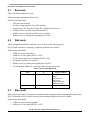
In Figure 1 we can view the dependencies among these modules:
Using Low Power modes on Kinetis family, Rev. 0
2
Freescale Semiconductor
System Clock Generation
Figure 1. MCG Configuration
The system oscillator and the RTC oscillator are the external sources that you can use to feed the MCG.
The OSC module is a crystal oscillator. The module, in conjunction with an external crystal or resonator,
generates a reference clock for the MCU.
The RTC oscillator module provides the clock source for the RTC. The RTC oscillator module, in
conjunction with an external crystal, generates a reference clock for the RTC.
In addition you have the option of selecting between two internal reference clocks as the input source for
the MCG as follows:
• Slow IRC (32 kHz) and Fast IRC (4 MHz)
These internal clocks are part of the MCG module.
The MCG module controls which clock source is used to derive the system clocks. The clock generation
logic divides the selected clock source into a variety of clock domains, including the clocks for the system
bus masters, system bus slaves, and flash memory.
In summary there are 4 input clock sources that can be used as the clock generator for the microcontroller,
you should select the source depending on the requirements of your application.
Module dependencies:
• All modules are dependent on the MCG for one or more of their clocks
• Oscillator module relies on the MCG for the control signals.
• The oscillator must be set up correctly, from within the MCG, before it is used
• System clock dividers must be setup before increasing the MCGOUT frequency to ensure the maximum
clock rate is not exceeded.
Using Low Power modes on Kinetis family, Rev. 0
Freescale Semiconductor
3
System Clock Generation
•
•
•
MCG is powered in all low power modes except very low leakage stop modes.
Crystal oscillator pins are XTAL and EXTAL by default out of reset.
There is no clock gating associated with the MCG module itself.
There are in total 9 different modes of operation for the MCG: FEI, FEE, FBI, FBE, PBE, PEE, BLPI,
BLPE, and Stop.
In the following chapter you can view important details of the system clock setup in the different low
power modes.
For more details in each specific module you can refer to the device Reference Manual.
3.1
•
•
•
•
•
Functionality of the system clock in low power modes
STOP - Normal Stop Mode
— Can enter STOP from any MCG mode
— Can optionally keep the PLL enabled but the output will be gated off - C5[PLLSTEN]
— Can optionally keep the internal reference clock enabled – C1[IREFSTEN]
— Can optionally keep the external reference clock enabled – OSC_CR[EREFSTEN]
— Will exit STOP in the same MCG mode when STOP was entered
– The exception to this if STOP is entered when in PEE mode and PLLSTEN=0, in this case
the MCG will be in PBE mode when STOP is exited
VLPR – Very Low Power Run Mode
— Can enter VLPR from BLPI mode with the fast IRC selected.
— Can enter VLPR from BLPE mode if the external clock is 4 MHz max.
— Will exit VLPR in the same MCG mode when VLPR was entered (BLPI or BLPE)
VLPW – Very Low Power Wait Mode
— Can enter VLPW from BLPI mode with the fast IRC selected.
— Can enter VLPW from BLPE mode if the external clock is 4 MHz max.
— Will exit VLPW in the same MCG mode when VLPW was entered (BLPI or BLPE)
— Can optionally keep the external reference clock enabled (4 MHz max.)
VLPS – Very Low Power Stop
— Can enter VLPS from any MCG mode
— Can optionally keep the external reference clock enabled (4 MHz max.)
— MCG is static with no clocks active (IREFSTEN and PLLSTEN have no effect)
— Will exit VLPS in the same MCG mode when VLPS was entered
– The exception to this if VLPS is entered when in PEE mode, in this case the MCG will be
in PBE mode when VLPS is exited
LLS – Low Leakage Stop
— Can enter LLS from any MCG mode
Using Low Power modes on Kinetis family, Rev. 0
4
Freescale Semiconductor
Description and usage of low power modes
•
4
— Can optionally keep the external reference clock enabled in low range and low power oscillator
mode (32 kHz)
— MCG is static with no clocks active (IREFSTEN and PLLSTEN have no effect)
— Will exit LLS in the same MCG mode when LLS was entered
– The exception to this if LLS is entered when in PEE mode, in this case the MCG will be in
PBE mode when LLS is exited
VLLS0/1/2/3 – Very Low Leakage Stop
— Can enter VLLSx from any MCG mode
— MCG is off, no clocks active, register states are not maintained
— Will exit in FEI mode (reset state)
— Can optionally keep the external reference clock enabled in low range and low power oscillator
mode (32 kHz). Must reconfigure the oscillator before clearing the ACKISO bit.
Description and usage of low power modes
The operating modes described in this chapter apply for the Kinetis family devices.
The available modes of operation are the following:
• Run
• Wait
• Stop
• VLPR (Very Low Power Run)
• VLPW (Very Low Power Wait)
• VLPS (Very Low Power Stop)
• LLS (Low Leakage Stop)
• VLLS3 (Very Low Leakage Stop3)
• VLLS2 (Very Low Leakage Stop2)
• VLLS1 (Very Low Leakage Stop1)
• VLLS0 (Very Low Leakage Stop0) 1
• BAT (Backup battery only)
In this chapter we will discuss details about all modes of operation relevant to the topic of this application note. That
is all modes except the Run and BAT.
NOTE
For a full description of the operating modes refer to the device reference
manual, search for chapter “Power modes”.
1. This mode of operation is present only in the 50 MHz devices. It has two modes of operation: Power On reset detect circuit
enabled or disabled.
Using Low Power modes on Kinetis family, Rev. 0
Freescale Semiconductor
5
Description and usage of low power modes
4.1
Run mode
This is the default mode out of reset.
Allows maximum performance of the chip.
Mode of operation details:
• Selected after any Reset
• On chip voltage regulator is on, full capability
• Stack pointer (SP), Program Counter (PC) and link register are set
• ARM processor exits reset and reads the start SP
• ARM processor reads the start PC from vector table
• Reduce power by clearing clock gating bits in SCGCx
4.2
Wait mode
Allows peripherals to function while the core is in sleep mode, reducing power.
NVIC remains sensitive to interrupts; peripherals continue to be clocked.
Mode of operation details:
• ARM core enters Sleep Mode
• ARM core is clock gated (HCLK = OFF)
• NVIC remains sensitive to interrupts (FCLK = ON)
• Peripherals continue to be clocked
• Reduce power by clearing clock gating bits in SCGCx
• On interrupt the ARM core exits Sleep Mode: Resume processing
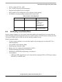
Table 1. How to enter Wait mode
From
4.3
To
Trigger conditions
Run
Wait
Execute WAIT( ); - This
means
that sleep-now or
sleep-on-exit
modes entered with
SLEEPDEEP clear
Wait
Run
Interrupt or Reset
Stop mode
Places chip in static state. Lowest power mode that retains all registers while maintaining LVD protection.
NVIC is disabled; AWIC is used to wake up from interrupt; peripheral clocks are stopped.
Mode of operation details:
• ARM core enters DeepSleep Mode
• ARM core is clock gated (HCLK = OFF)
Using Low Power modes on Kinetis family, Rev. 0
6
Freescale Semiconductor
Description and usage of low power modes
•
•
•
•
•
NVIC is disable (FCLK = OFF)
WIC is used to wake up from interruptions
Platform and peripheral clock are stopped
MCG module can be configured to leave reference clocks running
All SRAM is operating (content retained and I/O states held)
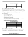
Table 2. How to enter Stop mode
From
4.4
To
Trigger Conditions
Run
Stop
Execute STOP( ); This
means
that sleep-now or
sleep-on-exit
modes entered with
SLEEPDEEP set
Stop
Run
Interrupt or Reset – Interrupt
goes to ISR (no LLWU)
VLPR (Very Low Power Run)
On-chip voltage regulator is in a low power mode that supplies only enough power to run the chip at a
reduced frequency. Reduced frequency Flash access mode (1 MHz); LVD off; internal oscillator provides
a low power 4 MHz source for the core, the bus and the peripheral clocks.
Mode of operation details:
•
•
•
•
•
•
•
On chip voltage regulator is in a mode that supplies only enough power to run the MCU in a
reduced frequency
Core and Bus clock limited to 4Mhz
Flash frequency limited to 1Mhz
Reduce power by clearing clock gating bits in SCGCx
Flash programming and erasing is not allowed
FlexMemory (EEPROM) programming is not allowed
Clock Monitor:
— CME0 and CME1 should also be set to a logic 0 before entering VLPR or VLPW power modes
if the MCG is in BLPE mode.
Using Low Power modes on Kinetis family, Rev. 0
Freescale Semiconductor
7
Description and usage of low power modes
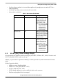
Table 3. How to enter VLPR mode
From
4.5
To
Trigger Conditions
Run
VLPR
Reduce system bus and
core frequency to 2 MHz or
less
Flash access frequency
limited to
1 MHz, AVLP = 1
Set RUNM = 10
Note: Poll VLPRS bit before
executing VLPR
specific code
(You can wait ~5 s
instead of waiting for
VLPRS)
VLPR
Run
Set RUNM = 00 or Interrupt
with LPWUI = 1 or Reset
Note: Poll REGONS bit
before increasing
frequency.
VLPW (Very Low Power Wait)
Same as VLPR but with the core in sleep mode to further reduce power; NVIC remains sensitive to
interrupts (FCLK = ON). On-chip voltage regulator is in a low power mode that supplies only enough
power to run the chip at a reduced frequency.
Mode of operation details:
•
•
•
•
•
•
•
ARM core enters Sleep Mode
ARM core is clock gated (HCLK = OFF)
NVIC remains sensitive to interrupts (FCLK = ON)
On chip voltage regulator is in a mode that supplies only enough power to run the MCU in a
reduced frequency
System and Bus clock limited to 4Mhz
Reduce power by clearing clock gating bits in SCGCx
Clock Monitor:
— CME0 and CME1 should also be set to a logic 0 before entering VLPR or VLPW power modes
if the MCG is in BLPE mode.
Using Low Power modes on Kinetis family, Rev. 0
8
Freescale Semiconductor
Description and usage of low power modes
Table 4. How to enter VLPW mode
From
4.6
To
Trigger Conditions
VLPR
VLPW
Execute WAIT( );
VLPW
VLPR
Interrupt with LPWUI = 0
VLPW
RUN
Interrupt with LPWUI = 1 or
Reset
VLPS (Very Low Power Stop)
Places chip in static state with LVD operation off. Lowest power mode with ADC and pin interrupts
functional. Peripheral clocks are stopped, but LPTimer, RTC, CMP, TSI can be used. NVIC is disabled
(FCLK =OFF), AWIC is used to wake up from interrupt.
On-chip voltage regulator is in a low power mode that supplies only enough power to run the chip at a
reduced frequency. All SRAM is operating (content retained and I/O states held).
Mode of operation details:
•
•
•
•
•
•
•
•
ARM core enters DeepSleep Mode
ARM core is clock gated (HCLK = OFF)
NVIC is disable (FCLK = OFF)
WIC is used to wake up from interruptions
Platform and peripheral clock are stopped
MCG module can be configured to leave reference clocks running
On chip voltage regulator is in a mode that supplies only enough power to run the MCU in a
reduced frequency
All SRAM is operating (content retained and I/O states held)
Table 5. How to enter VLPS mode
From
4.7
To
Trigger Conditions
VLPR
VLPS
STOPM = 000 or 010,
execute STOP( );
VLPS
VLPR
Interrupt with LPWUI = 0
RUN
VLPS
AVLP=1, STOPM =010,
execute STOP( );
VLPS
RUN
Interrupt with LPWUI= 1 or
Reset
LLS (Low Leakage Stop)
State retention power mode. Most peripherals are in state retention mode (with clocks stopped), but
LLWU, LPTimer, RTC, CMP, TSI can be used. NVIC is disabled, LLWU is used to wake up.
Using Low Power modes on Kinetis family, Rev. 0
Freescale Semiconductor
9
Description and usage of low power modes
NOTE
The LLWU interrupt must not be masked by the interrupt controller to avoid
a scenario where the system does not fully exit stop mode on an LLS
recovery.
All SRAM is operating (content retained and I/O states held).
Mode of operation details:
• ARM core enters Deep Sleep Mode
• ARM core is clock gated (HCLK = OFF)
• NVIC is disable (FCLK = OFF)
• LLWU is used to wake up from interruptions
• Platform and peripheral clock are stopped
• MCG module can be configured to leave reference clocks running
• On chip voltage regulator is in a mode that supplies only enough power to run the MCU in a
reduced frequency
• All SRAM is operating (content retained and I/O states held)
• Most of peripherals are in state retention mode (cannot operate)
Table 6. How to enter LLS mode
From
4.8
To
Trigger Conditions
Run
LLS
Set ALLS in PMPROT,
PMCTRL_STOPM = 011,
Execute STOP( );
LLS
Run
Wakeup from enabled LLWU
pin or module source or
Reset pin
VLPR
LLS
Set ALLS in PMPROT,
PMCTRL_STOPM = 011,
Execute STOP( );
VLLS3 (Very Low Leakage Stop3)
Most peripherals are disabled (with clocks stopped), but LLWU, LPTimer, RTC, CMP, TSI can be used.
NVIC is disabled, LLWU is used to wake up. SRAM_U and SRAM_L remain powered on (content
retained and I/O states held).
Mode of operation details:
• ARM core enters SleepDeep Mode
•
•
•
•
•
ARM core is clock gated (HCLK = OFF)
NVIC is disable (FCLK = OFF)
LLWU should configure by user to enable the desire wake up source
Platform and peripheral clock are stopped
MCG module can be configured to leave reference clocks running
Using Low Power modes on Kinetis family, Rev. 0
10
Freescale Semiconductor
Description and usage of low power modes
•
On chip voltage regulator is in a mode that supplies only enough power to run the MCU in a
reduced frequency
•
•
All SRAM is operating (content retained and I/O states held)
Most modules are disabled
Table 7. How to enter VLLS3 mode
From
4.9
To
Trigger Conditions
Run
VLLS (3,2,1,0)
Set AVLLSx in PMPROT,
PMCTRL_STOPM = 100
VLLSM = 011 for VLLS3,
010 for VLLS2, 001 for
VLLS1, 000 for VLLS0
Note: For VLLS0 you must
set or clear PORPO to
disable or enable
(respectively) the
POR detect circuit.
Execute STOP( );
VLLS (3,2,1,0)
Run
Wakeup from enabled LLWU
input source or Reset. All
wakeup goes through Reset
sequence. Check SRS for
source of wakeup. Check
VLLSM for mode
VLPR
VLLS(3,2,1,0)
Set AVLLSx in PMPROT,
PMCTRL_STOPM = 100
VLLSM = 011 for VLLS3,
010 =for VLLS2, 001 for
VLLS1, 000 for VLLS0
Note: For VLLS0 you must
set or clear PORPO to
disable or enable
(respectively) the
POR detect circuit.
Execute STOP( );
VLLS2 (Very Slow Leakage Stop2)
Most peripherals are disabled (with clocks stopped), but LLWU, LPTimer, RTC, CMP, TSI can be used.
NVIC is disabled; LLWU is used to wake up.
SRAM_L is powered off. A portion of SRAM_U remains powered on (content retained and I/O states
held).
Mode of operation details:
• ARM core enters SleepDeep Mode
• ARM core is clock gated (HCLK = OFF)
• NVIC is disable (FCLK = OFF)
• LLWU should configure by user to enable the desire wake up source
• Platform and peripheral clock are stopped
Using Low Power modes on Kinetis family, Rev. 0
Freescale Semiconductor
11
Description and usage of low power modes
•
•
•
•
MCG module can be configured to leave reference clocks running
On chip voltage regulator is in a mode that supplies only enough power to run the MCU in a
reduced frequency
Only partial SRAM is operating (content retained and I/O state held)
Most modules are disabled
Table 8. How to enter VLLS2 mode
From
4.10
To
Trigger Conditions
Run
VLLS (3,2,1,0)
Set AVLLSx in PMPROT,
PMCTRL_STOPM = 100
VLLSM = 011 for VLLS3,
010 for VLLS2, 001 for
VLLS1, 000 for VLLS0
Note: For VLLS0 you must
set or clear PORPO to
disable or enable
(respectively) the
POR detect circuit.
Execute STOP( );
VLLS(3,2,1,0)
Run
Wakeup from enabled LLWU
input source or Reset. All
wakeup goes through Reset
sequence. Check SRS for
source of wakeup. Check
VLLSM for mode
VLPR
VLLS(3,2,1,0)
Set AVLLSx in PMPROT,
PMCTRL_STOPM = 100
VLLSM = 011 for VLLS3,
010 for VLLS2, 001 for
VLLS1, 000 for VLLS0
Note: For VLLS0 you must
set or clear PORPO to
disable or enable
(respectively) the
POR detect circuit.
Execute STOP( );
VLLS1 (Very Low Leakage Stop1)
Most peripherals are disabled (with clocks stopped), but LLWU, LPTimer, RTC, CMP, TSI can be used.
NVIC is disabled; LLWU is used to wake up.
All of SRAM_U and SRAM_L are powered off. The 32-byte system register file and the 32-byte VBAT
register file remain powered for customer-critical data.
Mode of operation details:
•
•
•
•
ARM core enters SleepDeep Mode
ARM core is clock gated (HCLK = OFF)
NVIC is disable (FCLK = OFF)
LLWU should configure by user to enable the desire wake up source
Using Low Power modes on Kinetis family, Rev. 0
12
Freescale Semiconductor
Description and usage of low power modes
•
•
•
•
•
Platform and peripheral clock are stopped
MCG module can be configured to leave reference clocks running
On chip voltage regulator is in a mode that supplies only enough power to run the MCU in a
reduced frequency
All SRAM is powered down, only 32 byte register content retained and I/O states held
Most modules are disabled
Table 9. How to enter VLLS1 mode
From
4.11
To
Trigger Conditions
Run
VLLS (3,2,1,0)
Set AVLLSx in PMPROT,
PMCTRL_STOPM = 100
VLLSM = 011 for VLLS3,
010 for VLLS2, 001 for
VLLS1, 000 for VLLS0
Note: For VLLS0 you must
set or clear PORPO to
disable or enable
(respectively) the
POR detect circuit.
Execute STOP( );
VLLS(3,2,1,0)
Run
Wakeup from enabled LLWU
input source or Reset. All
wakeup goes through Reset
sequence. Check SRS for
source of wakeup. Check
VLLSM for mode.
VLPR
VLLS (3,2,1,0)
Set AVLLSx in PMPROT,
PMCTRL_STOPM = 100
VLLSM = 011 for VLLS3,
010 for VLLS2, 001 for
VLLS1, 000 for VLLS0
Note: For VLLS0 you must
set or clear PORPO to
disable or enable
(respectively) the
POR detect circuit.
Execute STOP( );
VLLS0 (Very Low Leakage Stop0)
LLWU, RTC. All SRAM powered off.
Mode of operation details:
• ARM core enters SleepDeep Mode
• ARM core is clock gated (HCLK = OFF)
• NVIC is disabled (FCLK = OFF)
• LLWU should configure by user to enable the desire wake up source
• Platform and peripheral clocks are stopped
Using Low Power modes on Kinetis family, Rev. 0
Freescale Semiconductor
13
Module operation in Low Power modes
•
•
MCG module can be configured to leave reference clocks running
On chip voltage regulator is in a mode that supplies only enough power to run the MCU in a reduced
frequency
•
•
All SRAM powered off.
Most modules are disabled except LLWU and RTC
Table 10. How to enter VLLS0 mode
From
5
To
Trigger Conditions
Run
VLLS (3,2,1,0)
Set AVLLSx in PMPROT,
PMCTRL_STOPM = 100
VLLSM = 011 for VLLS3,
010 for VLLS2, 001 for
VLLS1, 000
for VLLS0
Note: For VLLS0 you must
set or clear PORPO to
disable or enable
(respectively) the
POR detect circuit.
Execute STOP( );
VLLS (3,2,1,0)
Run
Wakeup from enabled LLWU
input source or Reset. All
wakeup goes through Reset
sequence. Check SRS for
source of wakeup. Check
VLLSM for mode.
VLPR
VLLS (3,2,1,0)
Set AVLLSx in PMPROT,
PMCTRL_STOPM = 100
VLLSM = 011 for VLLS3,
010 for VLLS2, 001 for
VLLS1, 000 for VLLS0
Note: For VLLS0 you must
set or clear PORPO to
disable or enable
(respectively) the
POR detect circuit.
Execute STOP( );
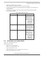
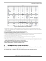
Module operation in Low Power modes
In this chapter we can view the microcontroller’s module status among the different power modes.
In order to choose the most proper low power mode for your application you must first make a list of the
modules that need to be enabled.
The following table is useful to decide what low power mode your application should enter based on the
modules that you require to be enabled.
Meaning of the terms used in the table:
• FF: Full functionality
Using Low Power modes on Kinetis family, Rev. 0
14
Freescale Semiconductor
Module operation in Low Power modes
•
•
•
•
•
Static: Module register states and associated memories are retained
Powered: Memory is powered to retain contents
Low power: Flash has a low power state that retains configuration registers to support faster
wakeup
Off: Modules are powered off; module is in reset state upon wakeup
Wakeup: Modules can serve as a wakeup source for the chip
For further details you can refer to the device Reference Manual, chapter “Module Operation in Low
Power Modes”.
Using Low Power modes on Kinetis family, Rev. 0
Freescale Semiconductor
15
Module operation in Low Power modes
Using Low Power modes on Kinetis family, Rev. 0
16
Freescale Semiconductor
Allowed power mode transitions
Figure 2. Module operation in low power modes
1. Using the LLWU module, the external pins available for this chip do not require the associated peripheral function to be
enabled. It only requires the function controlling the pin (GPIO or peripheral) to be configured as an input to allow a transition
to occur to the LLWU.
2. Since LPO clock source is disabled, filters will be bypassed during VLLS0.
3. The VLLSCTRL[PORPO] bit in the SMC module controls this option.
4. A 8 KB portion of SRAM_U block is left powered on in low power mode VLLS2.
5. FlexRAM enabled as EEPROM is not writable in VLPR and writes are ignored. Read accesses to FlexRAM as EEPROM while
in VLPR are allowed. There are no access restrictions for FlexRAM configured as traditional RAM.
6. These components remain powered in BAT power mode.
7. Use an externally generated bit clock or an externally generated audio master clock (including EXTAL).
8. System OSC and LPO clock sources are not available in VLLS0.
9. CMP in Stop or VLPS supports high speed or low speed external pin to pin or external pin to DAC compares. CMP in LLS or
VLLSx only supports low speed external pin to pin or external pin to DAC compares. Windowed, sampled & filtered modes of
operation are not available while in stop, VLPS, LLS, or VLLSx modes.
10. TSI wakeup from LLS and VLLSx modes is limited to a single selectable pin.
11. System OSC and LPO clock sources are not available in VLLS0.
6
Allowed power mode transitions
This chapter is a brief overview of the allowed power mode transitions. It is important to keep in mind that
there are restrictions for switch among all power modes.
The following figure is intended to help you visualize the power mode transitions allowed:
Using Low Power modes on Kinetis family, Rev. 0
Freescale Semiconductor
17
Allowed power mode transitions
Figure 3. Power mode state transition diagram
As given in the figure above not all mode transitions are allowed, for example if the device is in VLLSx
mode and you want to change to Stop mode you must first bring back the device to Run mode and then
switch to Stop mode.
Any reset always brings the chip back to the normal run state.
For more details refer to chapter “Power mode transitions” in the device Reference Manual.
Using Low Power modes on Kinetis family, Rev. 0
18
Freescale Semiconductor
Demo to enter power modes
7
Demo to enter power modes
In this chapter we will review the necessary conditions to enter the available power modes based on the
demo software.
The objective of this demo is to get familiar with the steps needed to enter the available power modes in
the Kinetis family of devices.
It is important to clarify that this demo uses only one mode to exit from any operation mode, but there are
many ways to exit from any given operation mode as previously explained in this document.
This demo is prepared to run on TWR-K20D50M with a K20DX128 device.
Low Power exit modes:
External pin SW2 has been enabled to wake up via the LLWU from any LLS and VLLSx mode, all wakeup
interrupts from these modes must go through LLWU_ISR.
All other modes (non-leakage) can be taken out of low power mode via an interrupt from any of the
available port enabled pins, in the case of this demo that is SW2 or SW3.
The following is required:
1. IAR Embedded Workbench for ARM v6.30 or CodeWarrior MCU V10.1 (with MCU 10.1 Kinetis
50MHz Service Pack installed)
2. TWR-K20D50M tower board.
3. P&E OSBDM OSJTAG Virtual Serial Toolkit.
You can download it from the following site:
http://www.pemicro.com/osbdm/index.cfm
4. Demo project: “low_power_demo”.
This toolkit contains the P&E terminal utility that you need to visualize the menu options via serial over
USB.
Before running the demo you need to configure your IDE to the proper settings depending on the
programming/debugging interface that you will use.
NOTE
If your preferred debug interface is already installed you can disregard the
following section and go directly to chapter 7.2 “Steps to run the demo”.
7.1
Flash programming and debugging settings
In this section we indicate the settings needed to program and debug you application into the Kinetis board
using IAR or CodeWarrior IDEs with any of the following debug interfaces: OSJTAG, P&E Multilink,
Segger J-Link.
IAR and OSJTAG/P&E Multilink
Flashloader FlashK20Xxxx must be used for these connections.
Using Low Power modes on Kinetis family, Rev. 0
Freescale Semiconductor
19
Demo to enter power modes
Unzip iar_FlashK20Xxxx_8k_ram.zip located in the demo project zip file and follow the instructions
below.
1. Place all of the files in this zip (except “readme.txt”) in your IAR Systems\Embedded
Workbench.6.0_x\arm\config\flashloader\Freescale folder
NOTE
This applies for the current IAR version IAR 6.30.4, for newer versions
these steps will not be necessary.
2. Open your IAR workspace file and select a flash configuration for the project
a) Open IAR Embedded Workbench IDE.
b) Open the low_power_demo workspace.
To do this you can drag and drop the “low_power_demo.eww” located on the following path:
{Demo Installation path}\build\iar\low_power_demo
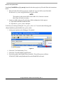
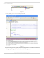
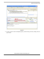
3. In the project options select Debugger->Download.
Figure 4.
4. Check the "Use flash loader(s)" box.
5. Check the "Override default .board file box".
6. Provide the path to the FlashK20Xxxx.board file. This will be given as follows:
$TOOLKIT_DIR$\config\flashloader\Freescale\FlashK20Xxxx.board.
Using Low Power modes on Kinetis family, Rev. 0
20
Freescale Semiconductor
Demo to enter power modes
Figure 5.
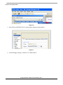
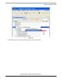
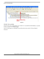
7. On debugger select driver PE_micro.
Figure 6.
Using Low Power modes on Kinetis family, Rev. 0
Freescale Semiconductor
21
Demo to enter power modes
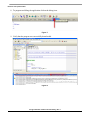
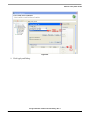
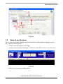
8. To program and debug the application click on the debug icon.
Figure 7.
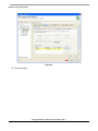
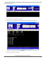
9. Verify that the program was successfully downloaded.
Figure 8.
Using Low Power modes on Kinetis family, Rev. 0
22
Freescale Semiconductor
Demo to enter power modes
10. At this point we have successfully downloaded the application, now we need to exit and close the
debugger by clicking on the X mark as shown in the following screen below:
Figure 9.
NOTE
The purpose of stopping the debug session is due to higher current
consumption measurements when the debugger is active.
IAR and J-link
For proper operation you must use: J-Link DLL V4.36i
You can download it from the following site:
http://www.segger.com/jlink-software.html?step=1&file=JLink_436kl
IAR must be configured as follows:
1. Open your IAR workspace file and select a flash configuration for the project.
2. Open IAR Embedded Workbench IDE.
3. Open the low_power_demo workspace.
To do this you can drag and drop the “low_power_demo.eww” located on the following path:
{Demo Installation path}\build\iar\low_power_demo
4. In the project options select General options.
Using Low Power modes on Kinetis family, Rev. 0
Freescale Semiconductor
23
Demo to enter power modes
Figure 10.
5. Select Device MK20DX128xxx5 on the project options as shown below:
Figure 11.
6. In the Debugger category: Uncheck “Use flash loaders”.
Using Low Power modes on Kinetis family, Rev. 0
24
Freescale Semiconductor
Demo to enter power modes
Figure 12.
7. In J-link/J-trace Connection window: Select JTAG interface.
Figure 13.
8. To program and debug the application click on the debug icon.
Using Low Power modes on Kinetis family, Rev. 0
Freescale Semiconductor
25
Demo to enter power modes
Figure 14.
9. Verify that the program was successfully downloaded.
Figure 15.
10. At this point we have successfully downloaded the application, now we need to exit and close the
debugger by clicking on the X mark as shown in the following screen:
Using Low Power modes on Kinetis family, Rev. 0
26
Freescale Semiconductor
Demo to enter power modes
Figure 16.
NOTE
The purpose of stopping the debug session is due to higher current
consumption measurements when the debugger is active.
CW MCU V10.1 and OSJTAG/ P&E Multilink
For proper operation with CW10.1, it must be configured as follows:
Update the flash programmer:
1. Click on Flash programmer and import “Flash Task”.
Using Low Power modes on Kinetis family, Rev. 0
Freescale Semiconductor
27
Demo to enter power modes
Figure 17.
2. Open the ARM folder, select K20DX128.xml and click Open.
Figure 18.
3. Select FLASH configuration.
Using Low Power modes on Kinetis family, Rev. 0
28
Freescale Semiconductor
Demo to enter power modes
Figure 19.
4. Build the project by clicking on the hammer icon as shown below:
Using Low Power modes on Kinetis family, Rev. 0
Freescale Semiconductor
29
Demo to enter power modes
Figure 20.
5. Click on the drop down arrow to select the corresponding debug configuration.
Figure 21.
6. Select FLASH_OSJTAG, go to Debugger tab, open Download section, uncheck “Perform Standard
Download”.
Using Low Power modes on Kinetis family, Rev. 0
30
Freescale Semiconductor
Demo to enter power modes
Figure 22.
7. Check the box for Execute Tasks, select the current task and click on Remove.
Using Low Power modes on Kinetis family, Rev. 0
Freescale Semiconductor
31
Demo to enter power modes
Figure 23.
8. Click on Add button and select K20DX128.
Using Low Power modes on Kinetis family, Rev. 0
32
Freescale Semiconductor
Demo to enter power modes
Figure 24.
9. Click Apply and Debug.
Using Low Power modes on Kinetis family, Rev. 0
Freescale Semiconductor
33
Demo to enter power modes
Figure 25.
10. Verify download.
Using Low Power modes on Kinetis family, Rev. 0
34
Freescale Semiconductor
Demo to enter power modes
Figure 26.
11. In order to measure current consumption properly, terminate debug session by clicking on the red
square button.
Using Low Power modes on Kinetis family, Rev. 0
Freescale Semiconductor
35
Demo to enter power modes
Figure 27.
CW MCU V10.1 and JLink
Follow the same steps as indicated above (for CW MCU V10.1 and OSJTAG/ P&E Multilink), except that
in step 6, you must select FLASH_Segger.
Select FLASH_Segger, go to Debugger tab, open Download section, uncheck “Perform Standard
Download”.
Using Low Power modes on Kinetis family, Rev. 0
36
Freescale Semiconductor
Demo to enter power modes
Figure 28.
7.2
Steps to run the demo
Once you have successfully loaded the application to the device and stopped the debugger, you can
proceed with the following steps:
1. Open the Terminal application from P&E.
2. Set the port to Port: USB COM, Baud: 115200,Parity: None, Bits: 8 Click on “Open Serial Port”.
Figure 29.
3. Make sure the port is successfully opened.
Using Low Power modes on Kinetis family, Rev. 0
Freescale Semiconductor
37
Demo to enter power modes
Figure 30.
4. Now click on the reset button of your board.
5. If you look to the Terminal Window you should have all available options displayed.
Figure 31.
6. Follow the instructions on the menu.
Using Low Power modes on Kinetis family, Rev. 0
38
Freescale Semiconductor
Demo to enter power modes
Example:
To enter Stop Mode:
• Type letter B in the terminal window.
The following message will be displayed:
Figure 32.
•
Press any key.
The following message is displayed:
Using Low Power modes on Kinetis family, Rev. 0
Freescale Semiconductor
39
Demo to enter power modes
Figure 33.
This means we are currently in stop mode.
• To measure power consumption (depending on your board) you should take off the Jumper that corresponds
to MCU power connections.
This is J25 on the TWR-K20D50M Rev. C
NOTE
If you are unsure of the corresponding jumper please refer to your tower
board user manual.
•
Now measure the device consumption between these terminals:
You must be measuring approximately 320A.
• If you want to exit this low power mode and enter another one press SW2 or SW3:
Using Low Power modes on Kinetis family, Rev. 0
40
Freescale Semiconductor
Conclusion
Figure 34.
Now you can follow the steps again to enter a new power mode.
NOTE
You can exit any power mode via reset.
8
Conclusion
When designing for low power you must take into consideration both hardware and software, as both
variables are equally important to design a successful power efficient application.
Remember the basics, set pins to a known state, higher core frequency and higher temperature both translate to
higher power consumption, disable clocks to unused modules.
9
References
The chapters in this application note contain a summary of the most important details of each topic.
For more details on any of the topics of this document you can refer to the following:
Information about power consumption:
Using Low Power modes on Kinetis family, Rev. 0
Freescale Semiconductor
41
References
•
Refer to the device datasheet
Search for “Power consumption operating behaviors”
Information and details about power modes:
• Refer to the device Reference Manual
Search for chapter “Power Management”
Using Low Power modes on Kinetis family, Rev. 0
42
Freescale Semiconductor