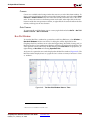
Download Xilinx UG029 ChipScope Pro Software and Cores User Guide v7.1

Transcript
ChipScope Pro
Software and Cores
User Guide
(ChipScope Pro Software v7.1i)
UG029 (v7.1) February 16, 2005
R
R
Xilinx is disclosing this Document and Intellectual Property (hereinafter “the Design”) to you for use in the development of designs
to operate on, or interface with Xilinx FPGAs. Except as stated herein, none of the Design may be copied, reproduced,
distributed, republished, downloaded, displayed, posted, or transmitted in any form or by any means including, but not limited to,
electronic, mechanical, photocopying, recording, or otherwise, without the prior written consent of Xilinx. Any unauthorized use
of the Design may violate copyright laws, trademark laws, the laws of privacy and publicity, and communications regulations and
statutes.
Xilinx does not assume any liability arising out of the application or use of the Design; nor does Xilinx convey any license under
its patents, copyrights, or any rights of others. You are responsible for obtaining any rights you may require for your use or
implementation of the Design. Xilinx reserves the right to make changes, at any time, to the Design as deemed desirable in the
sole discretion of Xilinx. Xilinx assumes no obligation to correct any errors contained herein or to advise you of any correction if
such be made. Xilinx will not assume any liability for the accuracy or correctness of any engineering or technical support or
assistance provided to you in connection with the Design.
THE DESIGN IS PROVIDED “AS IS" WITH ALL FAULTS, AND THE ENTIRE RISK AS TO ITS FUNCTION AND
IMPLEMENTATION IS WITH YOU. YOU ACKNOWLEDGE AND AGREE THAT YOU HAVE NOT RELIED ON ANY ORAL OR
WRITTEN INFORMATION OR ADVICE, WHETHER GIVEN BY XILINX, OR ITS AGENTS OR EMPLOYEES. XILINX MAKES
NO OTHER WARRANTIES, WHETHER EXPRESS, IMPLIED, OR STATUTORY, REGARDING THE DESIGN, INCLUDING ANY
WARRANTIES OF MERCHANTABILITY, FITNESS FOR A PARTICULAR PURPOSE, TITLE, AND NONINFRINGEMENT OF
THIRD-PARTY RIGHTS.
IN NO EVENT WILL XILINX BE LIABLE FOR ANY CONSEQUENTIAL, INDIRECT, EXEMPLARY, SPECIAL, OR INCIDENTAL
DAMAGES, INCLUDING ANY LOST DATA AND LOST PROFITS, ARISING FROM OR RELATING TO YOUR USE OF THE
DESIGN, EVEN IF YOU HAVE BEEN ADVISED OF THE POSSIBILITY OF SUCH DAMAGES. THE TOTAL CUMULATIVE
LIABILITY OF XILINX IN CONNECTION WITH YOUR USE OF THE DESIGN, WHETHER IN CONTRACT OR TORT OR
OTHERWISE, WILL IN NO EVENT EXCEED THE AMOUNT OF FEES PAID BY YOU TO XILINX HEREUNDER FOR USE OF
THE DESIGN. YOU ACKNOWLEDGE THAT THE FEES, IF ANY, REFLECT THE ALLOCATION OF RISK SET FORTH IN THIS
AGREEMENT AND THAT XILINX WOULD NOT MAKE AVAILABLE THE DESIGN TO YOU WITHOUT THESE LIMITATIONS OF
LIABILITY.
The Design is not designed or intended for use in the development of on-line control equipment in hazardous environments
requiring fail-safe controls, such as in the operation of nuclear facilities, aircraft navigation or communications systems, air traffic
control, life support, or weapons systems (“High-Risk Applications”). Xilinx specifically disclaims any express or implied
warranties of fitness for such High-Risk Applications. You represent that use of the Design in such High-Risk Applications is fully
at your risk.
© 2005 Xilinx, Inc. All rights reserved. XILINX, the Xilinx logo, and other designated brands included herein are trademarks of
Xilinx, Inc. PowerPC is a trademark of IBM, Inc. All other trademarks are the property of their respective owners.
ChipScope Pro Software and Cores User Guide
www.xilinx.com
UG029 (v7.1) February 16, 2005
Revision History
The following table shows the revision history for this document.
Date
Version
Revision
04/09/02
1.0
Initial Xilinx release.
10/29/02
5.1
Added new Chapter 3 “Using the ChipScope Pro Core Inserter”;
Old Chapter 3 is new Chapter 4 “Using the ChipScope Pro Analyzer”;
Updated all chapters to be compatible with 5.1i tools;
Revised version number to be in sync with version of tools.
03/06/03
5.2
Updated all chapters to be compatible with 5.2i tools;
Updated version number to reflect version number of tools.
05/15/03
5.2.2
8/29/03
6.1
Updated all chapters to be compatible with 6.1i tools;
Updated version number to reflect version number of tools;
Added Chapter 5 “Tcl/JTAG Interface”
02/13/04
6.2
Updated all chapters to be compatible with 6.2i tools;
Updated version number to reflect version number of tools;
Chapter 2: Added the “Generating the ATC2 Core” section;
Updated all chapters to reflect ATC2 compatibility;
Miscellaneous edits for clarity or continuity.
06/30/04
6.3
Updated all chapters to be compatible with 6.3i tools;
Updated version number to reflect version number of tools;
Miscellaneous edits for clarity or continuity;
Added MultiPRO cable information.
10/04/04
6.3.1
02/16/05
7.1
Chapter 1: Added the “Choice of Match Unit Counter” section to Table 1-3;
Chapter 2: Added the “Selecting Match Unit Counter Width” section; updated several
“trigger” screen shots;
Chapter 3: Added “Selecting Match Unit Counter Width” section;
Chapter 4: Updated screen shots in the “Configuring the Target Device(s)” section;
Added “Displaying Configuration Status Information” section;
Updated “Counter” section;
Added notes to the “Depth” and “Samples per Trigger” sections;
Updated “The VIO Console Window” section and most of its screen shots.
Minor text corrections.
Updated all chapters to be compatible with 7.1i tools;
Updated version number to reflect version number of tools;
Updated ATC2 core description to include the new auto-setup and “always on” features;
Added information regarding Analyzer support on Linux and Solaris;
Added information on the client/server remote debug feature;
Added Platform Cable USB cable information;
Miscellaneous edits for clarity or continuity.
UG029 (v7.1) February 16, 2005
www.xilinx.com
ChipScope Pro Software and Cores User Guide
www.xilinx.com
UG029 (v7.1) February 16, 2005
Table of Contents
Preface: About This User Guide
Chapter 1: Introduction
ChipScope Pro Tools Overview. . . . . . . . . . . . . . . . . . . . . . . . . . . . . . . . . . . . . . . . . . . . . . 1-1
ChipScope Pro Tools Description. . . . . . . . . . . . . . . . . . . . . . . . . . . . . . . . . . . . . . . . . . . . 1-1
Design Flow . . . . . . . . . . . . . . . . . . . . . . . . . . . . . . . . . . . . . . . . . . . . . . . . . . . . . . . . . . . . . 1-4
ChipScope Pro Cores Description . . . . . . . . . . . . . . . . . . . . . . . . . . . . . . . . . . . . . . . . . . . 1-4
ICON Core . . . . . . . . . . . . . . . . . . . . . . . . . . . . . . . . . . . . . . . . . . . . . . . . . . . . . . . . . . . . . . 1-4
ILA Core . . . . . . . . . . . . . . . . . . . . . . . . . . . . . . . . . . . . . . . . . . . . . . . . . . . . . . . . . . . . . . . . 1-5
ILA Trigger Input Logic . . . . . . . . . . . . . . . . . . . . . . . . . . . . . . . . . . . . . . . . . . . . . . . . . 1-5
ILA Trigger Output Logic . . . . . . . . . . . . . . . . . . . . . . . . . . . . . . . . . . . . . . . . . . . . . . . 1-10
ILA Data Capture Logic . . . . . . . . . . . . . . . . . . . . . . . . . . . . . . . . . . . . . . . . . . . . . . . . 1-10
ILA Control and Status Logic . . . . . . . . . . . . . . . . . . . . . . . . . . . . . . . . . . . . . . . . . . . . 1-11
ILA/ATC Core . . . . . . . . . . . . . . . . . . . . . . . . . . . . . . . . . . . . . . . . . . . . . . . . . . . . . . . . . . 1-11
ILA/ATC Trigger Input Logic . . . . . . . . . . . . . . . . . . . . . . . . . . . . . . . . . . . . . . . . . . . 1-11
ILA/ATC Trigger Output Logic . . . . . . . . . . . . . . . . . . . . . . . . . . . . . . . . . . . . . . . . . . 1-11
ILA/ATC Data Capture Logic . . . . . . . . . . . . . . . . . . . . . . . . . . . . . . . . . . . . . . . . . . . 1-12
ILA/ATC Control and Status Logic . . . . . . . . . . . . . . . . . . . . . . . . . . . . . . . . . . . . . . . 1-13
IBA/OPB Core . . . . . . . . . . . . . . . . . . . . . . . . . . . . . . . . . . . . . . . . . . . . . . . . . . . . . . . . . . 1-14
IBA/OPB Protocol Violation Monitor Logic . . . . . . . . . . . . . . . . . . . . . . . . . . . . . . . . . 1-14
IBA/OPB Trigger Input Logic . . . . . . . . . . . . . . . . . . . . . . . . . . . . . . . . . . . . . . . . . . . 1-16
IBA/OPB Trigger Output Logic . . . . . . . . . . . . . . . . . . . . . . . . . . . . . . . . . . . . . . . . . . 1-16
IBA/OPB Data Capture Logic . . . . . . . . . . . . . . . . . . . . . . . . . . . . . . . . . . . . . . . . . . . 1-18
IBA/OPB Control and Status Logic . . . . . . . . . . . . . . . . . . . . . . . . . . . . . . . . . . . . . . . 1-18
IBA/PLB Core . . . . . . . . . . . . . . . . . . . . . . . . . . . . . . . . . . . . . . . . . . . . . . . . . . . . . . . . . . 1-18
IBA/PLB Trigger Input Logic . . . . . . . . . . . . . . . . . . . . . . . . . . . . . . . . . . . . . . . . . . . . 1-18
IBA/PLB Trigger Output Logic . . . . . . . . . . . . . . . . . . . . . . . . . . . . . . . . . . . . . . . . . . 1-21
IBA/PLB Data Capture Logic . . . . . . . . . . . . . . . . . . . . . . . . . . . . . . . . . . . . . . . . . . . . 1-21
IBA/PLB Control and Status Logic . . . . . . . . . . . . . . . . . . . . . . . . . . . . . . . . . . . . . . . . 1-21
VIO Core . . . . . . . . . . . . . . . . . . . . . . . . . . . . . . . . . . . . . . . . . . . . . . . . . . . . . . . . . . . . . . . 1-22
Activity Detectors . . . . . . . . . . . . . . . . . . . . . . . . . . . . . . . . . . . . . . . . . . . . . . . . . . . . . 1-22
Pulse Trains . . . . . . . . . . . . . . . . . . . . . . . . . . . . . . . . . . . . . . . . . . . . . . . . . . . . . . . . . 1-22
ATC2 Core . . . . . . . . . . . . . . . . . . . . . . . . . . . . . . . . . . . . . . . . . . . . . . . . . . . . . . . . . . . . . . 1-23
ATC2 Data Path Description . . . . . . . . . . . . . . . . . . . . . . . . . . . . . . . . . . . . . . . . . . . . . 1-23
ATC2 Core Data Capture and Run-Time Control . . . . . . . . . . . . . . . . . . . . . . . . . . . . . 1-23
ICON and ILA Core Resource Usage . . . . . . . . . . . . . . . . . . . . . . . . . . . . . . . . . . . . . . . 1-24
Synthesis Requirements . . . . . . . . . . . . . . . . . . . . . . . . . . . . . . . . . . . . . . . . . . . . . . . . . . 1-25
System Requirements . . . . . . . . . . . . . . . . . . . . . . . . . . . . . . . . . . . . . . . . . . . . . . . . . . . . . . 1-25
Software Tools Requirements . . . . . . . . . . . . . . . . . . . . . . . . . . . . . . . . . . . . . . . . . . . . . 1-25
Communications Requirements . . . . . . . . . . . . . . . . . . . . . . . . . . . . . . . . . . . . . . . . . . . 1-25
Board Requirements . . . . . . . . . . . . . . . . . . . . . . . . . . . . . . . . . . . . . . . . . . . . . . . . . . . . . 1-27
Host System Requirements for Windows 2000/XP . . . . . . . . . . . . . . . . . . . . . . . . . . . 1-27
Host System Requirements for Linux . . . . . . . . . . . . . . . . . . . . . . . . . . . . . . . . . . . . . . . 1-27
Host System Requirements for Solaris 2.8 and 2.9 . . . . . . . . . . . . . . . . . . . . . . . . . . . . 1-28
ChipScope Pro Software and Cores User Guide
UG029 (v7.1) February 16, 2005
www.xilinx.com
v
R
ChipScope Pro Software Installation . . . . . . . . . . . . . . . . . . . . . . . . . . . . . . . . . . . . . . . 1-29
Installing ChipScope Pro Software for Windows 2000/XP . . . . . . . . . . . . . . . . . . . . . 1-29
Installing ChipScope Pro Software for Solaris 2.8 and 2.9 . . . . . . . . . . . . . . . . . . . . . . 1-30
Installing ChipScope Pro Software for Linux . . . . . . . . . . . . . . . . . . . . . . . . . . . . . . . . 1-31
Installing the Java Run-time Environment . . . . . . . . . . . . . . . . . . . . . . . . . . . . . . . . . . . 1-31
Chapter 2: Using the ChipScope Pro Core Generator
Core Generator Overview . . . . . . . . . . . . . . . . . . . . . . . . . . . . . . . . . . . . . . . . . . . . . . . . . . . 2-1
Generating an ICON Core . . . . . . . . . . . . . . . . . . . . . . . . . . . . . . . . . . . . . . . . . . . . . . . . . . . 2-1
General ICON Core Options . . . . . . . . . . . . . . . . . . . . . . . . . . . . . . . . . . . . . . . . . . . . . . . 2-2
Choosing the File Destination . . . . . . . . . . . . . . . . . . . . . . . . . . . . . . . . . . . . . . . . . . . . . 2-3
Selecting the Target Device Family . . . . . . . . . . . . . . . . . . . . . . . . . . . . . . . . . . . . . . . . . 2-3
Entering the Number of Control Ports . . . . . . . . . . . . . . . . . . . . . . . . . . . . . . . . . . . . . . 2-3
Disabling the Boundary Scan Component Instance . . . . . . . . . . . . . . . . . . . . . . . . . . . . 2-3
Selecting the Boundary Scan Chain . . . . . . . . . . . . . . . . . . . . . . . . . . . . . . . . . . . . . . . . 2-3
Disabling JTAG Clock BUFG Insertion . . . . . . . . . . . . . . . . . . . . . . . . . . . . . . . . . . . . . . 2-4
Including Boundary Scan Ports . . . . . . . . . . . . . . . . . . . . . . . . . . . . . . . . . . . . . . . . . . . 2-4
Creating Example Templates . . . . . . . . . . . . . . . . . . . . . . . . . . . . . . . . . . . . . . . . . . . . . . . 2-5
HDL Example Files . . . . . . . . . . . . . . . . . . . . . . . . . . . . . . . . . . . . . . . . . . . . . . . . . . . . . 2-5
Batch Mode Generation Argument Example Files . . . . . . . . . . . . . . . . . . . . . . . . . . . . . 2-5
Generating the Core . . . . . . . . . . . . . . . . . . . . . . . . . . . . . . . . . . . . . . . . . . . . . . . . . . . . . . . 2-6
Using the ICON Core . . . . . . . . . . . . . . . . . . . . . . . . . . . . . . . . . . . . . . . . . . . . . . . . . . . . . 2-6
Generating an ILA Core . . . . . . . . . . . . . . . . . . . . . . . . . . . . . . . . . . . . . . . . . . . . . . . . . . . . . 2-7
General ILA Core Options . . . . . . . . . . . . . . . . . . . . . . . . . . . . . . . . . . . . . . . . . . . . . . . . . 2-8
Choosing the File Destination . . . . . . . . . . . . . . . . . . . . . . . . . . . . . . . . . . . . . . . . . . . . . 2-8
Selecting the Target Device Family . . . . . . . . . . . . . . . . . . . . . . . . . . . . . . . . . . . . . . . . . 2-8
Using SRL16s . . . . . . . . . . . . . . . . . . . . . . . . . . . . . . . . . . . . . . . . . . . . . . . . . . . . . . . . . 2-9
Using RPMs . . . . . . . . . . . . . . . . . . . . . . . . . . . . . . . . . . . . . . . . . . . . . . . . . . . . . . . . . . 2-9
Selecting the Clock Edge . . . . . . . . . . . . . . . . . . . . . . . . . . . . . . . . . . . . . . . . . . . . . . . . . 2-9
ILA Core Trigger Port Options . . . . . . . . . . . . . . . . . . . . . . . . . . . . . . . . . . . . . . . . . . . . . 2-9
Selecting the Number of Trigger Ports . . . . . . . . . . . . . . . . . . . . . . . . . . . . . . . . . . . . . 2-10
Entering the Width of the Trigger Ports . . . . . . . . . . . . . . . . . . . . . . . . . . . . . . . . . . . . 2-10
Selecting the Number of Trigger Match Units . . . . . . . . . . . . . . . . . . . . . . . . . . . . . . . 2-10
Selecting the Match Unit Type . . . . . . . . . . . . . . . . . . . . . . . . . . . . . . . . . . . . . . . . . . . 2-11
Selecting Match Unit Counter Width . . . . . . . . . . . . . . . . . . . . . . . . . . . . . . . . . . . . . . 2-12
Enabling the Trigger Condition Sequencer . . . . . . . . . . . . . . . . . . . . . . . . . . . . . . . . . . 2-12
Enabling the Storage Qualification Condition . . . . . . . . . . . . . . . . . . . . . . . . . . . . . . . 2-12
Enabling the Trigger Output Port . . . . . . . . . . . . . . . . . . . . . . . . . . . . . . . . . . . . . . . . . 2-12
ILA Core Data Port Options . . . . . . . . . . . . . . . . . . . . . . . . . . . . . . . . . . . . . . . . . . . . . . . 2-13
Selecting the Data Depth . . . . . . . . . . . . . . . . . . . . . . . . . . . . . . . . . . . . . . . . . . . . . . . . 2-14
Selecting the Data Type . . . . . . . . . . . . . . . . . . . . . . . . . . . . . . . . . . . . . . . . . . . . . . . . 2-15
Entering the Data Width . . . . . . . . . . . . . . . . . . . . . . . . . . . . . . . . . . . . . . . . . . . . . . . . 2-15
Selecting the Data-Same-As-Trigger Ports . . . . . . . . . . . . . . . . . . . . . . . . . . . . . . . . . . 2-15
Number of Block RAMs . . . . . . . . . . . . . . . . . . . . . . . . . . . . . . . . . . . . . . . . . . . . . . . . 2-16
Creating Example Templates . . . . . . . . . . . . . . . . . . . . . . . . . . . . . . . . . . . . . . . . . . . . . . 2-16
HDL Example Files . . . . . . . . . . . . . . . . . . . . . . . . . . . . . . . . . . . . . . . . . . . . . . . . . . . . 2-16
Bus/Signal Name Example Files (*.cdc) . . . . . . . . . . . . . . . . . . . . . . . . . . . . . . . . . . . . 2-17
Batch Mode Generation Argument Example Files . . . . . . . . . . . . . . . . . . . . . . . . . . . . 2-17
Generating the Core . . . . . . . . . . . . . . . . . . . . . . . . . . . . . . . . . . . . . . . . . . . . . . . . . . . . . . 2-17
Using the ILA Core . . . . . . . . . . . . . . . . . . . . . . . . . . . . . . . . . . . . . . . . . . . . . . . . . . . . . . 2-18
vi
www.xilinx.com
ChipScope Pro Software and Cores User Guide
UG029 (v7.1) February 16, 2005
R
Generating an ILA/ATC Core. . . . . . . . . . . . . . . . . . . . . . . . . . . . . . . . . . . . . . . . . . . . . . . 2-19
General ILA/ATC Core Options . . . . . . . . . . . . . . . . . . . . . . . . . . . . . . . . . . . . . . . . . . . 2-20
Choosing the File Destination . . . . . . . . . . . . . . . . . . . . . . . . . . . . . . . . . . . . . . . . . . . . 2-20
Selecting the Target Device Family . . . . . . . . . . . . . . . . . . . . . . . . . . . . . . . . . . . . . . . . 2-20
Using SRL16s . . . . . . . . . . . . . . . . . . . . . . . . . . . . . . . . . . . . . . . . . . . . . . . . . . . . . . . . 2-20
Using RPMs . . . . . . . . . . . . . . . . . . . . . . . . . . . . . . . . . . . . . . . . . . . . . . . . . . . . . . . . . 2-21
Selecting the Clock Edge . . . . . . . . . . . . . . . . . . . . . . . . . . . . . . . . . . . . . . . . . . . . . . . . 2-21
ILA/ATC Core Trigger Port Options . . . . . . . . . . . . . . . . . . . . . . . . . . . . . . . . . . . . . . . 2-21
Selecting the Number of Trigger Ports . . . . . . . . . . . . . . . . . . . . . . . . . . . . . . . . . . . . . 2-22
Entering the Width of the Trigger Ports . . . . . . . . . . . . . . . . . . . . . . . . . . . . . . . . . . . . 2-22
Selecting the Number of Trigger Match Units . . . . . . . . . . . . . . . . . . . . . . . . . . . . . . . 2-22
Selecting the Match Unit Type . . . . . . . . . . . . . . . . . . . . . . . . . . . . . . . . . . . . . . . . . . . 2-23
Selecting Match Unit Counter Width . . . . . . . . . . . . . . . . . . . . . . . . . . . . . . . . . . . . . . 2-24
Enabling the Trigger Condition Sequencer . . . . . . . . . . . . . . . . . . . . . . . . . . . . . . . . . . 2-24
Enabling the Trigger Output Port . . . . . . . . . . . . . . . . . . . . . . . . . . . . . . . . . . . . . . . . . 2-24
ILA/ATC Core Data Port Options . . . . . . . . . . . . . . . . . . . . . . . . . . . . . . . . . . . . . . . . . 2-25
Transmit Rate . . . . . . . . . . . . . . . . . . . . . . . . . . . . . . . . . . . . . . . . . . . . . . . . . . . . . . . . 2-25
Maximum CLK Port Frequency . . . . . . . . . . . . . . . . . . . . . . . . . . . . . . . . . . . . . . . . . . 2-25
Clock Resource Utilization . . . . . . . . . . . . . . . . . . . . . . . . . . . . . . . . . . . . . . . . . . . . . . 2-26
Number of Data Pins . . . . . . . . . . . . . . . . . . . . . . . . . . . . . . . . . . . . . . . . . . . . . . . . . . 2-26
Output Buffer Type . . . . . . . . . . . . . . . . . . . . . . . . . . . . . . . . . . . . . . . . . . . . . . . . . . . . 2-26
Output Clock and Data Pin Locations . . . . . . . . . . . . . . . . . . . . . . . . . . . . . . . . . . . . . 2-27
Data Width and Depth . . . . . . . . . . . . . . . . . . . . . . . . . . . . . . . . . . . . . . . . . . . . . . . . . 2-27
Creating Example Templates . . . . . . . . . . . . . . . . . . . . . . . . . . . . . . . . . . . . . . . . . . . . . . 2-28
HDL Example Files . . . . . . . . . . . . . . . . . . . . . . . . . . . . . . . . . . . . . . . . . . . . . . . . . . . . 2-28
Bus/Signal Name Example Files (*.cdc) . . . . . . . . . . . . . . . . . . . . . . . . . . . . . . . . . . . . 2-28
Batch Mode Generation Argument Example Files . . . . . . . . . . . . . . . . . . . . . . . . . . . . 2-29
Generating the Core . . . . . . . . . . . . . . . . . . . . . . . . . . . . . . . . . . . . . . . . . . . . . . . . . . . . . . 2-29
Using the ILA/ATC Core . . . . . . . . . . . . . . . . . . . . . . . . . . . . . . . . . . . . . . . . . . . . . . . . . 2-29
Generating the IBA/OPB Core . . . . . . . . . . . . . . . . . . . . . . . . . . . . . . . . . . . . . . . . . . . . . . 2-30
General IBA/OPB Core Options . . . . . . . . . . . . . . . . . . . . . . . . . . . . . . . . . . . . . . . . . . . 2-31
Choosing the File Destination . . . . . . . . . . . . . . . . . . . . . . . . . . . . . . . . . . . . . . . . . . . . 2-31
Selecting the Target Device Family . . . . . . . . . . . . . . . . . . . . . . . . . . . . . . . . . . . . . . . . 2-31
Using SRL16s . . . . . . . . . . . . . . . . . . . . . . . . . . . . . . . . . . . . . . . . . . . . . . . . . . . . . . . . 2-31
Using RPMs . . . . . . . . . . . . . . . . . . . . . . . . . . . . . . . . . . . . . . . . . . . . . . . . . . . . . . . . . 2-32
Selecting the Clock Edge . . . . . . . . . . . . . . . . . . . . . . . . . . . . . . . . . . . . . . . . . . . . . . . . 2-32
Selecting the OPB Bus Settings . . . . . . . . . . . . . . . . . . . . . . . . . . . . . . . . . . . . . . . . . . . 2-32
IBA/OPB Core Trigger Port Options . . . . . . . . . . . . . . . . . . . . . . . . . . . . . . . . . . . . . . . 2-34
Selecting the OPB Signal Groups as Trigger Ports . . . . . . . . . . . . . . . . . . . . . . . . . . . . 2-35
Entering the Width of the Trigger Ports . . . . . . . . . . . . . . . . . . . . . . . . . . . . . . . . . . . . 2-36
Selecting the Number of Trigger Match Units . . . . . . . . . . . . . . . . . . . . . . . . . . . . . . . 2-36
Selecting the Match Unit Type . . . . . . . . . . . . . . . . . . . . . . . . . . . . . . . . . . . . . . . . . . . 2-37
Selecting Match Unit Counter Width . . . . . . . . . . . . . . . . . . . . . . . . . . . . . . . . . . . . . . 2-38
Enabling the Trigger Condition Sequencer . . . . . . . . . . . . . . . . . . . . . . . . . . . . . . . . . . 2-38
Enabling the Storage Qualification Condition . . . . . . . . . . . . . . . . . . . . . . . . . . . . . . . 2-38
Enabling the Trigger Output Port . . . . . . . . . . . . . . . . . . . . . . . . . . . . . . . . . . . . . . . . . 2-38
IBA/OPB Core Data Port Options . . . . . . . . . . . . . . . . . . . . . . . . . . . . . . . . . . . . . . . . . . 2-39
Selecting the Data Depth . . . . . . . . . . . . . . . . . . . . . . . . . . . . . . . . . . . . . . . . . . . . . . . . 2-39
Selecting the Data Type . . . . . . . . . . . . . . . . . . . . . . . . . . . . . . . . . . . . . . . . . . . . . . . . 2-40
Entering the Data Width . . . . . . . . . . . . . . . . . . . . . . . . . . . . . . . . . . . . . . . . . . . . . . . . 2-41
Selecting the Data-Same-As-Trigger Ports . . . . . . . . . . . . . . . . . . . . . . . . . . . . . . . . . . 2-41
Number of Block RAMs . . . . . . . . . . . . . . . . . . . . . . . . . . . . . . . . . . . . . . . . . . . . . . . . 2-41
ChipScope Pro Software and Cores User Guide
UG029 (v7.1) February 16, 2005
www.xilinx.com
vii
R
Creating Example Templates . . . . . . . . . . . . . . . . . . . . . . . . . . . . . . . . . . . . . . . . . . . . . . 2-41
HDL Example Files . . . . . . . . . . . . . . . . . . . . . . . . . . . . . . . . . . . . . . . . . . . . . . . . . . . . 2-42
Bus/Signal Name Example Files (*.cdc) . . . . . . . . . . . . . . . . . . . . . . . . . . . . . . . . . . . . 2-42
Batch Mode Generation Argument Example Files . . . . . . . . . . . . . . . . . . . . . . . . . . . . 2-42
Generating the Core . . . . . . . . . . . . . . . . . . . . . . . . . . . . . . . . . . . . . . . . . . . . . . . . . . . . . . 2-43
Using the IBA/OPB Core . . . . . . . . . . . . . . . . . . . . . . . . . . . . . . . . . . . . . . . . . . . . . . . . . 2-43
Generating the IBA/PLB Core . . . . . . . . . . . . . . . . . . . . . . . . . . . . . . . . . . . . . . . . . . . . . . 2-44
General IBA/PLB Core Options . . . . . . . . . . . . . . . . . . . . . . . . . . . . . . . . . . . . . . . . . . . 2-45
Choosing the File Destination . . . . . . . . . . . . . . . . . . . . . . . . . . . . . . . . . . . . . . . . . . . . 2-45
Selecting the Target Device Family . . . . . . . . . . . . . . . . . . . . . . . . . . . . . . . . . . . . . . . . 2-45
Using SRL16s . . . . . . . . . . . . . . . . . . . . . . . . . . . . . . . . . . . . . . . . . . . . . . . . . . . . . . . . 2-45
Using RPMs . . . . . . . . . . . . . . . . . . . . . . . . . . . . . . . . . . . . . . . . . . . . . . . . . . . . . . . . . 2-46
Selecting the Clock Edge . . . . . . . . . . . . . . . . . . . . . . . . . . . . . . . . . . . . . . . . . . . . . . . . 2-46
Selecting the PLB Bus Settings . . . . . . . . . . . . . . . . . . . . . . . . . . . . . . . . . . . . . . . . . . . 2-46
IBA/PLB Core Trigger Port Options. . . . . . . . . . . . . . . . . . . . . . . . . . . . . . . . . . . . . . . . 2-46
Selecting the PLB Signal Groups as Trigger Ports . . . . . . . . . . . . . . . . . . . . . . . . . . . . . 2-47
Entering the Width of the Trigger Ports . . . . . . . . . . . . . . . . . . . . . . . . . . . . . . . . . . . . 2-49
Selecting the Number of Trigger Match Units . . . . . . . . . . . . . . . . . . . . . . . . . . . . . . . 2-49
Selecting the Match Unit Type . . . . . . . . . . . . . . . . . . . . . . . . . . . . . . . . . . . . . . . . . . . 2-50
Selecting Match Unit Counter Width . . . . . . . . . . . . . . . . . . . . . . . . . . . . . . . . . . . . . . 2-51
Enabling the Trigger Condition Sequencer . . . . . . . . . . . . . . . . . . . . . . . . . . . . . . . . . . 2-51
Enabling the Storage Qualification Condition . . . . . . . . . . . . . . . . . . . . . . . . . . . . . . . 2-51
Enabling the Trigger Output Port . . . . . . . . . . . . . . . . . . . . . . . . . . . . . . . . . . . . . . . . . 2-51
IBA/PLB Core Data Port Options . . . . . . . . . . . . . . . . . . . . . . . . . . . . . . . . . . . . . . . . . . 2-52
Selecting the Data Depth . . . . . . . . . . . . . . . . . . . . . . . . . . . . . . . . . . . . . . . . . . . . . . . . 2-52
Selecting the Data Type . . . . . . . . . . . . . . . . . . . . . . . . . . . . . . . . . . . . . . . . . . . . . . . . 2-53
Entering the Data Width . . . . . . . . . . . . . . . . . . . . . . . . . . . . . . . . . . . . . . . . . . . . . . . . 2-53
Selecting the Data-Same-As-Trigger Ports . . . . . . . . . . . . . . . . . . . . . . . . . . . . . . . . . . 2-54
Number of Block RAMs . . . . . . . . . . . . . . . . . . . . . . . . . . . . . . . . . . . . . . . . . . . . . . . . 2-54
Creating Example Templates . . . . . . . . . . . . . . . . . . . . . . . . . . . . . . . . . . . . . . . . . . . . . . 2-54
HDL Example Files . . . . . . . . . . . . . . . . . . . . . . . . . . . . . . . . . . . . . . . . . . . . . . . . . . . . 2-55
Bus/Signal Name Example Files (*.cdc) . . . . . . . . . . . . . . . . . . . . . . . . . . . . . . . . . . . . 2-55
Batch Mode Generation Argument Example Files . . . . . . . . . . . . . . . . . . . . . . . . . . . . 2-55
Generating the Core . . . . . . . . . . . . . . . . . . . . . . . . . . . . . . . . . . . . . . . . . . . . . . . . . . . . . . 2-56
Using the IBA/PLB Core . . . . . . . . . . . . . . . . . . . . . . . . . . . . . . . . . . . . . . . . . . . . . . . . . 2-56
Generating the VIO Core . . . . . . . . . . . . . . . . . . . . . . . . . . . . . . . . . . . . . . . . . . . . . . . . . . . 2-57
General VIO Core Options . . . . . . . . . . . . . . . . . . . . . . . . . . . . . . . . . . . . . . . . . . . . . . . . 2-58
Choosing the File Destination . . . . . . . . . . . . . . . . . . . . . . . . . . . . . . . . . . . . . . . . . . . . 2-58
Selecting the Target Device Family . . . . . . . . . . . . . . . . . . . . . . . . . . . . . . . . . . . . . . . . 2-58
Using SRL16s . . . . . . . . . . . . . . . . . . . . . . . . . . . . . . . . . . . . . . . . . . . . . . . . . . . . . . . . 2-58
Selecting Input/Output Port Settings . . . . . . . . . . . . . . . . . . . . . . . . . . . . . . . . . . . . . . 2-59
Selecting the Clock Edge . . . . . . . . . . . . . . . . . . . . . . . . . . . . . . . . . . . . . . . . . . . . . . . . 2-59
Creating Example Templates . . . . . . . . . . . . . . . . . . . . . . . . . . . . . . . . . . . . . . . . . . . . . . 2-60
HDL Example Files . . . . . . . . . . . . . . . . . . . . . . . . . . . . . . . . . . . . . . . . . . . . . . . . . . . . 2-60
Batch Mode Generation Argument Example Files . . . . . . . . . . . . . . . . . . . . . . . . . . . . 2-61
Generating the Core . . . . . . . . . . . . . . . . . . . . . . . . . . . . . . . . . . . . . . . . . . . . . . . . . . . . . . 2-61
Using the VIO Core . . . . . . . . . . . . . . . . . . . . . . . . . . . . . . . . . . . . . . . . . . . . . . . . . . . . . . 2-61
Generating the ATC2 Core . . . . . . . . . . . . . . . . . . . . . . . . . . . . . . . . . . . . . . . . . . . . . . . . . 2-62
General ATC2 Core Options . . . . . . . . . . . . . . . . . . . . . . . . . . . . . . . . . . . . . . . . . . . . . . 2-63
Choosing the File Destination . . . . . . . . . . . . . . . . . . . . . . . . . . . . . . . . . . . . . . . . . . . . 2-63
Selecting the Target Device Family . . . . . . . . . . . . . . . . . . . . . . . . . . . . . . . . . . . . . . . . 2-63
Selecting the Clock Edge . . . . . . . . . . . . . . . . . . . . . . . . . . . . . . . . . . . . . . . . . . . . . . . . 2-63
viii
www.xilinx.com
ChipScope Pro Software and Cores User Guide
UG029 (v7.1) February 16, 2005
R
ATC2 Core Data Options . . . . . . . . . . . . . . . . . . . . . . . . . . . . . . . . . . . . . . . . . . . . . . . . . 2-64
Capture Mode . . . . . . . . . . . . . . . . . . . . . . . . . . . . . . . . . . . . . . . . . . . . . . . . . . . . . . . . 2-65
Signal Bank Count . . . . . . . . . . . . . . . . . . . . . . . . . . . . . . . . . . . . . . . . . . . . . . . . . . . . 2-65
Driver Endpoint Type . . . . . . . . . . . . . . . . . . . . . . . . . . . . . . . . . . . . . . . . . . . . . . . . . . 2-65
TDM Rate . . . . . . . . . . . . . . . . . . . . . . . . . . . . . . . . . . . . . . . . . . . . . . . . . . . . . . . . . . . 2-65
ATD Pin Count . . . . . . . . . . . . . . . . . . . . . . . . . . . . . . . . . . . . . . . . . . . . . . . . . . . . . . . 2-65
Data Port Width . . . . . . . . . . . . . . . . . . . . . . . . . . . . . . . . . . . . . . . . . . . . . . . . . . . . . . 2-65
Max Frequency Range . . . . . . . . . . . . . . . . . . . . . . . . . . . . . . . . . . . . . . . . . . . . . . . . . 2-65
Enable Auto Setup . . . . . . . . . . . . . . . . . . . . . . . . . . . . . . . . . . . . . . . . . . . . . . . . . . . . 2-66
Enable "Always On" Mode . . . . . . . . . . . . . . . . . . . . . . . . . . . . . . . . . . . . . . . . . . . . . . 2-66
Pin Edit Mode . . . . . . . . . . . . . . . . . . . . . . . . . . . . . . . . . . . . . . . . . . . . . . . . . . . . . . . . 2-66
Pin Parameters . . . . . . . . . . . . . . . . . . . . . . . . . . . . . . . . . . . . . . . . . . . . . . . . . . . . . . . 2-66
Core Utilization. . . . . . . . . . . . . . . . . . . . . . . . . . . . . . . . . . . . . . . . . . . . . . . . . . . . . . . 2-67
Creating ATC2 Example Templates . . . . . . . . . . . . . . . . . . . . . . . . . . . . . . . . . . . . . . . . 2-67
HDL Example Files . . . . . . . . . . . . . . . . . . . . . . . . . . . . . . . . . . . . . . . . . . . . . . . . . . . . 2-67
Bus/Signal Name Example Files (*.cdc) . . . . . . . . . . . . . . . . . . . . . . . . . . . . . . . . . . . . 2-69
Batch Mode Generation Argument Example Files . . . . . . . . . . . . . . . . . . . . . . . . . . . . 2-69
Generating the Core . . . . . . . . . . . . . . . . . . . . . . . . . . . . . . . . . . . . . . . . . . . . . . . . . . . . . . 2-69
Using the ATC2 Core. . . . . . . . . . . . . . . . . . . . . . . . . . . . . . . . . . . . . . . . . . . . . . . . . . . . . 2-70
Chapter 3: Using the ChipScope Pro Core Inserter
Core Inserter Overview. . . . . . . . . . . . . . . . . . . . . . . . . . . . . . . . . . . . . . . . . . . . . . . . . . . . . . 3-1
Using the Core Inserter with ISE Project Navigator . . . . . . . . . . . . . . . . . . . . . . . . . . 3-1
ChipScope Definition and Connection Source File . . . . . . . . . . . . . . . . . . . . . . . . . . . . . 3-1
Useful Project Navigator Settings . . . . . . . . . . . . . . . . . . . . . . . . . . . . . . . . . . . . . . . . . . . 3-3
Using the Core Inserter with Command Line Implementation . . . . . . . . . . . . . . . . 3-4
ChipScope Pro Core Inserter Features . . . . . . . . . . . . . . . . . . . . . . . . . . . . . . . . . . . . . . . 3-5
Working with Projects . . . . . . . . . . . . . . . . . . . . . . . . . . . . . . . . . . . . . . . . . . . . . . . . . . . . . 3-5
Opening an Existing Project . . . . . . . . . . . . . . . . . . . . . . . . . . . . . . . . . . . . . . . . . . . . . . 3-5
Saving Projects . . . . . . . . . . . . . . . . . . . . . . . . . . . . . . . . . . . . . . . . . . . . . . . . . . . . . . . . 3-5
Refreshing the Netlist . . . . . . . . . . . . . . . . . . . . . . . . . . . . . . . . . . . . . . . . . . . . . . . . . . . 3-6
Inserting and Removing Units . . . . . . . . . . . . . . . . . . . . . . . . . . . . . . . . . . . . . . . . . . . . 3-6
Setting Preferences . . . . . . . . . . . . . . . . . . . . . . . . . . . . . . . . . . . . . . . . . . . . . . . . . . . . . 3-6
Inserting the Cores . . . . . . . . . . . . . . . . . . . . . . . . . . . . . . . . . . . . . . . . . . . . . . . . . . . . . 3-6
Exiting the Core Inserter . . . . . . . . . . . . . . . . . . . . . . . . . . . . . . . . . . . . . . . . . . . . . . . . . 3-6
Specifying Input and Output Files . . . . . . . . . . . . . . . . . . . . . . . . . . . . . . . . . . . . . . . . . . 3-7
Project Level Parameters . . . . . . . . . . . . . . . . . . . . . . . . . . . . . . . . . . . . . . . . . . . . . . . . . . . 3-8
Selecting the Target Device Family . . . . . . . . . . . . . . . . . . . . . . . . . . . . . . . . . . . . . . . . . 3-8
Using SRL16s . . . . . . . . . . . . . . . . . . . . . . . . . . . . . . . . . . . . . . . . . . . . . . . . . . . . . . . . . 3-8
Using RPMs . . . . . . . . . . . . . . . . . . . . . . . . . . . . . . . . . . . . . . . . . . . . . . . . . . . . . . . . . . 3-9
Choosing ICON Options . . . . . . . . . . . . . . . . . . . . . . . . . . . . . . . . . . . . . . . . . . . . . . . . . . . 3-9
Disabling JTAG Clock BUFG Insertion . . . . . . . . . . . . . . . . . . . . . . . . . . . . . . . . . . . . . . 3-9
Choosing ILA or ILA/ATC Trigger Options and Parameters . . . . . . . . . . . . . . . . . . 3-10
Selecting the Number of Trigger Ports . . . . . . . . . . . . . . . . . . . . . . . . . . . . . . . . . . . . . 3-10
Entering the Width of the Trigger Ports . . . . . . . . . . . . . . . . . . . . . . . . . . . . . . . . . . . . 3-10
Selecting the Number of Trigger Match Units . . . . . . . . . . . . . . . . . . . . . . . . . . . . . . . 3-10
Selecting the Match Unit Type . . . . . . . . . . . . . . . . . . . . . . . . . . . . . . . . . . . . . . . . . . . 3-11
Selecting Match Unit Counter Width . . . . . . . . . . . . . . . . . . . . . . . . . . . . . . . . . . . . . . 3-12
Enabling the Trigger Condition Sequencer . . . . . . . . . . . . . . . . . . . . . . . . . . . . . . . . . . 3-12
Enabling the Storage Qualification Condition . . . . . . . . . . . . . . . . . . . . . . . . . . . . . . . 3-12
ChipScope Pro Software and Cores User Guide
UG029 (v7.1) February 16, 2005
www.xilinx.com
ix
R
Choosing ILA Core Capture Parameters . . . . . . . . . . . . . . . . . . . . . . . . . . . . . . . . . . . . 3-13
Selecting the Data Depth . . . . . . . . . . . . . . . . . . . . . . . . . . . . . . . . . . . . . . . . . . . . . . . . 3-14
Selecting the Data Type . . . . . . . . . . . . . . . . . . . . . . . . . . . . . . . . . . . . . . . . . . . . . . . . 3-15
Selecting the Data-Same-As-Trigger Ports . . . . . . . . . . . . . . . . . . . . . . . . . . . . . . . . . . 3-15
Entering the Data Width . . . . . . . . . . . . . . . . . . . . . . . . . . . . . . . . . . . . . . . . . . . . . . . . 3-16
Number of Block RAMs . . . . . . . . . . . . . . . . . . . . . . . . . . . . . . . . . . . . . . . . . . . . . . . . 3-16
Choosing ILA/ATC Capture Settings . . . . . . . . . . . . . . . . . . . . . . . . . . . . . . . . . . . . . . 3-16
Transmit Rate . . . . . . . . . . . . . . . . . . . . . . . . . . . . . . . . . . . . . . . . . . . . . . . . . . . . . . . . 3-16
Maximum CLK Port Frequency . . . . . . . . . . . . . . . . . . . . . . . . . . . . . . . . . . . . . . . . . . 3-17
Clock Resource Usage . . . . . . . . . . . . . . . . . . . . . . . . . . . . . . . . . . . . . . . . . . . . . . . . . . 3-17
Output Buffer Type . . . . . . . . . . . . . . . . . . . . . . . . . . . . . . . . . . . . . . . . . . . . . . . . . . . . 3-17
Number of Data Pins . . . . . . . . . . . . . . . . . . . . . . . . . . . . . . . . . . . . . . . . . . . . . . . . . . 3-18
Output Clock and Data Pin Locations . . . . . . . . . . . . . . . . . . . . . . . . . . . . . . . . . . . . . 3-18
Data Width and Depth . . . . . . . . . . . . . . . . . . . . . . . . . . . . . . . . . . . . . . . . . . . . . . . . . 3-18
Choosing ATC2 Data Capture Settings . . . . . . . . . . . . . . . . . . . . . . . . . . . . . . . . . . . . . 3-19
Capture Mode . . . . . . . . . . . . . . . . . . . . . . . . . . . . . . . . . . . . . . . . . . . . . . . . . . . . . . . . 3-20
Clock Edge . . . . . . . . . . . . . . . . . . . . . . . . . . . . . . . . . . . . . . . . . . . . . . . . . . . . . . . . . . 3-20
Max Frequency Range . . . . . . . . . . . . . . . . . . . . . . . . . . . . . . . . . . . . . . . . . . . . . . . . . 3-20
Enable Auto Setup . . . . . . . . . . . . . . . . . . . . . . . . . . . . . . . . . . . . . . . . . . . . . . . . . . . . 3-20
Enable "Always On" Mode . . . . . . . . . . . . . . . . . . . . . . . . . . . . . . . . . . . . . . . . . . . . . . 3-20
Pin Edit Mode . . . . . . . . . . . . . . . . . . . . . . . . . . . . . . . . . . . . . . . . . . . . . . . . . . . . . . . . 3-20
ATD Pin Count . . . . . . . . . . . . . . . . . . . . . . . . . . . . . . . . . . . . . . . . . . . . . . . . . . . . . . . 3-20
Endpoint Type . . . . . . . . . . . . . . . . . . . . . . . . . . . . . . . . . . . . . . . . . . . . . . . . . . . . . . . 3-21
Signal Bank Count . . . . . . . . . . . . . . . . . . . . . . . . . . . . . . . . . . . . . . . . . . . . . . . . . . . . 3-21
TDM Rate . . . . . . . . . . . . . . . . . . . . . . . . . . . . . . . . . . . . . . . . . . . . . . . . . . . . . . . . . . . 3-21
Data Width . . . . . . . . . . . . . . . . . . . . . . . . . . . . . . . . . . . . . . . . . . . . . . . . . . . . . . . . . . 3-21
Pin Parameters . . . . . . . . . . . . . . . . . . . . . . . . . . . . . . . . . . . . . . . . . . . . . . . . . . . . . . . 3-21
Core Utilization. . . . . . . . . . . . . . . . . . . . . . . . . . . . . . . . . . . . . . . . . . . . . . . . . . . . . . . 3-22
Choosing Net Connections for ILA or ILA/ATC Signals . . . . . . . . . . . . . . . . . . . . . . 3-23
Adding Units . . . . . . . . . . . . . . . . . . . . . . . . . . . . . . . . . . . . . . . . . . . . . . . . . . . . . . . . . . . 3-28
Inserting Cores into Netlist . . . . . . . . . . . . . . . . . . . . . . . . . . . . . . . . . . . . . . . . . . . . . . . . 3-28
Managing Project Preferences . . . . . . . . . . . . . . . . . . . . . . . . . . . . . . . . . . . . . . . . . . . . . 3-28
Chapter 4: Using the ChipScope Pro Analyzer
Analyzer Overview . . . . . . . . . . . . . . . . . . . . . . . . . . . . . . . . . . . . . . . . . . . . . . . . . . . . . . . . . 4-1
Analyzer Server Interface . . . . . . . . . . . . . . . . . . . . . . . . . . . . . . . . . . . . . . . . . . . . . . . . . . . 4-2
Analyzer Client Interface . . . . . . . . . . . . . . . . . . . . . . . . . . . . . . . . . . . . . . . . . . . . . . . . . . . . 4-3
Project Tree . . . . . . . . . . . . . . . . . . . . . . . . . . . . . . . . . . . . . . . . . . . . . . . . . . . . . . . . . . . . . . 4-3
Signal Browser . . . . . . . . . . . . . . . . . . . . . . . . . . . . . . . . . . . . . . . . . . . . . . . . . . . . . . . . . . . 4-3
Renaming Signals Buses, and Triggers Ports . . . . . . . . . . . . . . . . . . . . . . . . . . . . . . . . . 4-3
Adding/Removing Signals from Views . . . . . . . . . . . . . . . . . . . . . . . . . . . . . . . . . . . . . 4-4
Combining and Adding Signals Into Buses . . . . . . . . . . . . . . . . . . . . . . . . . . . . . . . . . . 4-4
Reverse Bus Ordering . . . . . . . . . . . . . . . . . . . . . . . . . . . . . . . . . . . . . . . . . . . . . . . . . . . 4-4
Bus Radices . . . . . . . . . . . . . . . . . . . . . . . . . . . . . . . . . . . . . . . . . . . . . . . . . . . . . . . . . . . 4-5
Deleting Buses . . . . . . . . . . . . . . . . . . . . . . . . . . . . . . . . . . . . . . . . . . . . . . . . . . . . . . . . 4-6
Type and Persistence (VIO only) . . . . . . . . . . . . . . . . . . . . . . . . . . . . . . . . . . . . . . . . . . 4-6
Message Pane . . . . . . . . . . . . . . . . . . . . . . . . . . . . . . . . . . . . . . . . . . . . . . . . . . . . . . . . . . . . 4-6
Main Window Area . . . . . . . . . . . . . . . . . . . . . . . . . . . . . . . . . . . . . . . . . . . . . . . . . . . . . . . 4-6
x
www.xilinx.com
ChipScope Pro Software and Cores User Guide
UG029 (v7.1) February 16, 2005
R
Analyzer Menu Features . . . . . . . . . . . . . . . . . . . . . . . . . . . . . . . . . . . . . . . . . . . . . . . . . . . . 4-7
Working with Projects . . . . . . . . . . . . . . . . . . . . . . . . . . . . . . . . . . . . . . . . . . . . . . . . . . . . . 4-7
Creating and Saving A New Project . . . . . . . . . . . . . . . . . . . . . . . . . . . . . . . . . . . . . . . . 4-7
Saving Projects . . . . . . . . . . . . . . . . . . . . . . . . . . . . . . . . . . . . . . . . . . . . . . . . . . . . . . . . 4-7
Printing Waveforms. . . . . . . . . . . . . . . . . . . . . . . . . . . . . . . . . . . . . . . . . . . . . . . . . . . . . . . 4-8
Print Wizard (1 of 3) Window . . . . . . . . . . . . . . . . . . . . . . . . . . . . . . . . . . . . . . . . . . . . . 4-9
Print Wizard (2 of 3) Window . . . . . . . . . . . . . . . . . . . . . . . . . . . . . . . . . . . . . . . . . . . . 4-11
Print Wizard (3 of 3) Window . . . . . . . . . . . . . . . . . . . . . . . . . . . . . . . . . . . . . . . . . . . . 4-12
Page Setup . . . . . . . . . . . . . . . . . . . . . . . . . . . . . . . . . . . . . . . . . . . . . . . . . . . . . . . . . . 4-13
Importing Signal Names . . . . . . . . . . . . . . . . . . . . . . . . . . . . . . . . . . . . . . . . . . . . . . . . . . 4-14
Exporting Data . . . . . . . . . . . . . . . . . . . . . . . . . . . . . . . . . . . . . . . . . . . . . . . . . . . . . . . . . . 4-15
Closing and Exiting the Analyzer . . . . . . . . . . . . . . . . . . . . . . . . . . . . . . . . . . . . . . . . . . 4-15
Viewing Options . . . . . . . . . . . . . . . . . . . . . . . . . . . . . . . . . . . . . . . . . . . . . . . . . . . . . . . . 4-15
Setting up a Server Host Connection . . . . . . . . . . . . . . . . . . . . . . . . . . . . . . . . . . . . . . . 4-16
Opening a Parallel Cable Connection . . . . . . . . . . . . . . . . . . . . . . . . . . . . . . . . . . . . . . . 4-17
Opening an Agilent E5904B Cable Connection . . . . . . . . . . . . . . . . . . . . . . . . . . . . . . . 4-18
Opening a MultiLINX connection . . . . . . . . . . . . . . . . . . . . . . . . . . . . . . . . . . . . . . . . . . 4-19
Opening a Platform Cable USB Connection . . . . . . . . . . . . . . . . . . . . . . . . . . . . . . . . . 4-19
Polling the Auto Core Status . . . . . . . . . . . . . . . . . . . . . . . . . . . . . . . . . . . . . . . . . . . . . . 4-20
Configuring the Target Device(s) . . . . . . . . . . . . . . . . . . . . . . . . . . . . . . . . . . . . . . . . . . 4-20
Setting Up the Boundary Scan (JTAG) Chain . . . . . . . . . . . . . . . . . . . . . . . . . . . . . . . . 4-20
Device Configuration . . . . . . . . . . . . . . . . . . . . . . . . . . . . . . . . . . . . . . . . . . . . . . . . . . 4-21
Observing Configuration Progress . . . . . . . . . . . . . . . . . . . . . . . . . . . . . . . . . . . . . . . . 4-22
Displaying JTAG User and ID Codes . . . . . . . . . . . . . . . . . . . . . . . . . . . . . . . . . . . . . . 4-22
Displaying Configuration Status Information . . . . . . . . . . . . . . . . . . . . . . . . . . . . . . . 4-23
Trigger Setup Window . . . . . . . . . . . . . . . . . . . . . . . . . . . . . . . . . . . . . . . . . . . . . . . . . . . 4-24
Capture Settings . . . . . . . . . . . . . . . . . . . . . . . . . . . . . . . . . . . . . . . . . . . . . . . . . . . . . . 4-25
Match Functions . . . . . . . . . . . . . . . . . . . . . . . . . . . . . . . . . . . . . . . . . . . . . . . . . . . . . . 4-28
Trigger Conditions . . . . . . . . . . . . . . . . . . . . . . . . . . . . . . . . . . . . . . . . . . . . . . . . . . . . 4-29
Saving and Recalling Trigger Setups . . . . . . . . . . . . . . . . . . . . . . . . . . . . . . . . . . . . . . 4-32
Running/Arming the Trigger . . . . . . . . . . . . . . . . . . . . . . . . . . . . . . . . . . . . . . . . . . . . 4-32
Stopping/Disarming the Trigger . . . . . . . . . . . . . . . . . . . . . . . . . . . . . . . . . . . . . . . . . 4-32
Waveform Window . . . . . . . . . . . . . . . . . . . . . . . . . . . . . . . . . . . . . . . . . . . . . . . . . . . . . . 4-33
Bus and Signal Reordering . . . . . . . . . . . . . . . . . . . . . . . . . . . . . . . . . . . . . . . . . . . . . . 4-33
Cut/Copy/Paste/Delete Signals and Buses . . . . . . . . . . . . . . . . . . . . . . . . . . . . . . . . . 4-33
Zooming In and Out . . . . . . . . . . . . . . . . . . . . . . . . . . . . . . . . . . . . . . . . . . . . . . . . . . . 4-34
Centering the Waveform. . . . . . . . . . . . . . . . . . . . . . . . . . . . . . . . . . . . . . . . . . . . . . . . 4-35
Cursors . . . . . . . . . . . . . . . . . . . . . . . . . . . . . . . . . . . . . . . . . . . . . . . . . . . . . . . . . . . . . 4-35
Sample Display Numbering . . . . . . . . . . . . . . . . . . . . . . . . . . . . . . . . . . . . . . . . . . . . . 4-35
Displaying Markers . . . . . . . . . . . . . . . . . . . . . . . . . . . . . . . . . . . . . . . . . . . . . . . . . . . 4-36
Listing Window . . . . . . . . . . . . . . . . . . . . . . . . . . . . . . . . . . . . . . . . . . . . . . . . . . . . . . . . . 4-36
Bus and Signal Reordering . . . . . . . . . . . . . . . . . . . . . . . . . . . . . . . . . . . . . . . . . . . . . . 4-36
Removing Signals/Buses . . . . . . . . . . . . . . . . . . . . . . . . . . . . . . . . . . . . . . . . . . . . . . . 4-36
Cursors . . . . . . . . . . . . . . . . . . . . . . . . . . . . . . . . . . . . . . . . . . . . . . . . . . . . . . . . . . . . . 4-37
Goto Cursors . . . . . . . . . . . . . . . . . . . . . . . . . . . . . . . . . . . . . . . . . . . . . . . . . . . . . . . . . 4-37
Bus Plot Window . . . . . . . . . . . . . . . . . . . . . . . . . . . . . . . . . . . . . . . . . . . . . . . . . . . . . . . . 4-37
Plot Type . . . . . . . . . . . . . . . . . . . . . . . . . . . . . . . . . . . . . . . . . . . . . . . . . . . . . . . . . . . . 4-38
Display Type . . . . . . . . . . . . . . . . . . . . . . . . . . . . . . . . . . . . . . . . . . . . . . . . . . . . . . . . . 4-38
Bus Selection . . . . . . . . . . . . . . . . . . . . . . . . . . . . . . . . . . . . . . . . . . . . . . . . . . . . . . . . . 4-38
Min/Max . . . . . . . . . . . . . . . . . . . . . . . . . . . . . . . . . . . . . . . . . . . . . . . . . . . . . . . . . . . 4-38
Cursor Tracking . . . . . . . . . . . . . . . . . . . . . . . . . . . . . . . . . . . . . . . . . . . . . . . . . . . . . . 4-38
ChipScope Pro Software and Cores User Guide
UG029 (v7.1) February 16, 2005
www.xilinx.com
xi
R
VIO Console Window . . . . . . . . . . . . . . . . . . . . . . . . . . . . . . . . . . . . . . . . . . . . . . . . . . . . 4-39
Bus/Signal Column . . . . . . . . . . . . . . . . . . . . . . . . . . . . . . . . . . . . . . . . . . . . . . . . . . . 4-40
Value Column . . . . . . . . . . . . . . . . . . . . . . . . . . . . . . . . . . . . . . . . . . . . . . . . . . . . . . . . 4-41
Global Console Controls . . . . . . . . . . . . . . . . . . . . . . . . . . . . . . . . . . . . . . . . . . . . . . . . 4-43
Help . . . . . . . . . . . . . . . . . . . . . . . . . . . . . . . . . . . . . . . . . . . . . . . . . . . . . . . . . . . . . . . . . . . 4-43
Viewing the Help Pages . . . . . . . . . . . . . . . . . . . . . . . . . . . . . . . . . . . . . . . . . . . . . . . . 4-43
ChipScope Pro Main Toolbar Features . . . . . . . . . . . . . . . . . . . . . . . . . . . . . . . . . . . . . . 4-44
ChipScope Pro Analyzer Command Line Options . . . . . . . . . . . . . . . . . . . . . . . . . . . 4-45
Optional Arguments . . . . . . . . . . . . . . . . . . . . . . . . . . . . . . . . . . . . . . . . . . . . . . . . . . . 4-45
Windows Command Line Example . . . . . . . . . . . . . . . . . . . . . . . . . . . . . . . . . . . . . . . 4-45
Chapter 5: Tcl/JTAG Interface
Overview . . . . . . . . . . . . . . . . . . . . . . . . . . . . . . . . . . . . . . . . . . . . . . . . . . . . . . . . . . . . . . . . . . . 5-1
Requirements . . . . . . . . . . . . . . . . . . . . . . . . . . . . . . . . . . . . . . . . . . . . . . . . . . . . . . . . . . . . 5-1
Limitations . . . . . . . . . . . . . . . . . . . . . . . . . . . . . . . . . . . . . . . . . . . . . . . . . . . . . . . . . . . . . . 5-1
Tcl/JTAG Command Summary . . . . . . . . . . . . . . . . . . . . . . . . . . . . . . . . . . . . . . . . . . . . . . 5-2
Command Details . . . . . . . . . . . . . . . . . . . . . . . . . . . . . . . . . . . . . . . . . . . . . . . . . . . . . . . . . . . 5-3
jtag_autodetect . . . . . . . . . . . . . . . . . . . . . . . . . . . . . . . . . . . . . . . . . . . . . . . . . . . . . . . . . . . 5-3
Syntax . . . . . . . . . . . . . . . . . . . . . . . . . . . . . . . . . . . . . . . . . . . . . . . . . . . . . . . . . . . . . . . 5-3
Required Arguments . . . . . . . . . . . . . . . . . . . . . . . . . . . . . . . . . . . . . . . . . . . . . . . . . . . 5-3
Returns . . . . . . . . . . . . . . . . . . . . . . . . . . . . . . . . . . . . . . . . . . . . . . . . . . . . . . . . . . . . . . 5-3
Example . . . . . . . . . . . . . . . . . . . . . . . . . . . . . . . . . . . . . . . . . . . . . . . . . . . . . . . . . . . . . 5-3
jtag_close . . . . . . . . . . . . . . . . . . . . . . . . . . . . . . . . . . . . . . . . . . . . . . . . . . . . . . . . . . . . . . . . 5-4
Syntax . . . . . . . . . . . . . . . . . . . . . . . . . . . . . . . . . . . . . . . . . . . . . . . . . . . . . . . . . . . . . . . 5-4
Required Arguments . . . . . . . . . . . . . . . . . . . . . . . . . . . . . . . . . . . . . . . . . . . . . . . . . . . 5-4
Returns . . . . . . . . . . . . . . . . . . . . . . . . . . . . . . . . . . . . . . . . . . . . . . . . . . . . . . . . . . . . . . 5-4
Example . . . . . . . . . . . . . . . . . . . . . . . . . . . . . . . . . . . . . . . . . . . . . . . . . . . . . . . . . . . . . 5-4
jtag_devicecount . . . . . . . . . . . . . . . . . . . . . . . . . . . . . . . . . . . . . . . . . . . . . . . . . . . . . . . . . . 5-5
Syntax . . . . . . . . . . . . . . . . . . . . . . . . . . . . . . . . . . . . . . . . . . . . . . . . . . . . . . . . . . . . . . . 5-5
Required Arguments . . . . . . . . . . . . . . . . . . . . . . . . . . . . . . . . . . . . . . . . . . . . . . . . . . . 5-5
Optional Arguments . . . . . . . . . . . . . . . . . . . . . . . . . . . . . . . . . . . . . . . . . . . . . . . . . . . . 5-5
Returns . . . . . . . . . . . . . . . . . . . . . . . . . . . . . . . . . . . . . . . . . . . . . . . . . . . . . . . . . . . . . . 5-5
Examples. . . . . . . . . . . . . . . . . . . . . . . . . . . . . . . . . . . . . . . . . . . . . . . . . . . . . . . . . . . . . 5-5
jtag_irlength . . . . . . . . . . . . . . . . . . . . . . . . . . . . . . . . . . . . . . . . . . . . . . . . . . . . . . . . . . . . . 5-6
Syntax . . . . . . . . . . . . . . . . . . . . . . . . . . . . . . . . . . . . . . . . . . . . . . . . . . . . . . . . . . . . . . . 5-6
Required Arguments . . . . . . . . . . . . . . . . . . . . . . . . . . . . . . . . . . . . . . . . . . . . . . . . . . . 5-6
Optional Arguments . . . . . . . . . . . . . . . . . . . . . . . . . . . . . . . . . . . . . . . . . . . . . . . . . . . . 5-6
Returns . . . . . . . . . . . . . . . . . . . . . . . . . . . . . . . . . . . . . . . . . . . . . . . . . . . . . . . . . . . . . . 5-6
Examples. . . . . . . . . . . . . . . . . . . . . . . . . . . . . . . . . . . . . . . . . . . . . . . . . . . . . . . . . . . . . 5-6
jtag_lock . . . . . . . . . . . . . . . . . . . . . . . . . . . . . . . . . . . . . . . . . . . . . . . . . . . . . . . . . . . . . . . . . 5-7
Syntax . . . . . . . . . . . . . . . . . . . . . . . . . . . . . . . . . . . . . . . . . . . . . . . . . . . . . . . . . . . . . . . 5-7
Required Arguments . . . . . . . . . . . . . . . . . . . . . . . . . . . . . . . . . . . . . . . . . . . . . . . . . . . 5-7
Optional Arguments . . . . . . . . . . . . . . . . . . . . . . . . . . . . . . . . . . . . . . . . . . . . . . . . . . . . 5-7
Returns . . . . . . . . . . . . . . . . . . . . . . . . . . . . . . . . . . . . . . . . . . . . . . . . . . . . . . . . . . . . . . 5-7
Example . . . . . . . . . . . . . . . . . . . . . . . . . . . . . . . . . . . . . . . . . . . . . . . . . . . . . . . . . . . . . 5-7
jtag_navigate . . . . . . . . . . . . . . . . . . . . . . . . . . . . . . . . . . . . . . . . . . . . . . . . . . . . . . . . . . . . . 5-8
Syntax . . . . . . . . . . . . . . . . . . . . . . . . . . . . . . . . . . . . . . . . . . . . . . . . . . . . . . . . . . . . . . . 5-8
Required Arguments . . . . . . . . . . . . . . . . . . . . . . . . . . . . . . . . . . . . . . . . . . . . . . . . . . . 5-8
Optional Arguments . . . . . . . . . . . . . . . . . . . . . . . . . . . . . . . . . . . . . . . . . . . . . . . . . . . . 5-8
Returns . . . . . . . . . . . . . . . . . . . . . . . . . . . . . . . . . . . . . . . . . . . . . . . . . . . . . . . . . . . . . . 5-8
Examples. . . . . . . . . . . . . . . . . . . . . . . . . . . . . . . . . . . . . . . . . . . . . . . . . . . . . . . . . . . . . 5-8
xii
www.xilinx.com
ChipScope Pro Software and Cores User Guide
UG029 (v7.1) February 16, 2005
R
jtag_open . . . . . . . . . . . . . . . . . . . . . . . . . . . . . . . . . . . . . . . . . . . . . . . . . . . . . . . . . . . . . . . . 5-9
Syntax . . . . . . . . . . . . . . . . . . . . . . . . . . . . . . . . . . . . . . . . . . . . . . . . . . . . . . . . . . . . . . . 5-9
Optional Arguments . . . . . . . . . . . . . . . . . . . . . . . . . . . . . . . . . . . . . . . . . . . . . . . . . . . . 5-9
Returns . . . . . . . . . . . . . . . . . . . . . . . . . . . . . . . . . . . . . . . . . . . . . . . . . . . . . . . . . . . . . 5-11
Examples. . . . . . . . . . . . . . . . . . . . . . . . . . . . . . . . . . . . . . . . . . . . . . . . . . . . . . . . . . . . 5-11
jtag_shiftir . . . . . . . . . . . . . . . . . . . . . . . . . . . . . . . . . . . . . . . . . . . . . . . . . . . . . . . . . . . . . . 5-12
Syntax . . . . . . . . . . . . . . . . . . . . . . . . . . . . . . . . . . . . . . . . . . . . . . . . . . . . . . . . . . . . . . 5-12
Required Arguments . . . . . . . . . . . . . . . . . . . . . . . . . . . . . . . . . . . . . . . . . . . . . . . . . . 5-12
Optional Arguments . . . . . . . . . . . . . . . . . . . . . . . . . . . . . . . . . . . . . . . . . . . . . . . . . . . 5-12
Returns . . . . . . . . . . . . . . . . . . . . . . . . . . . . . . . . . . . . . . . . . . . . . . . . . . . . . . . . . . . . . 5-12
Examples. . . . . . . . . . . . . . . . . . . . . . . . . . . . . . . . . . . . . . . . . . . . . . . . . . . . . . . . . . . . 5-13
jtag_shiftdr . . . . . . . . . . . . . . . . . . . . . . . . . . . . . . . . . . . . . . . . . . . . . . . . . . . . . . . . . . . . . 5-14
Syntax . . . . . . . . . . . . . . . . . . . . . . . . . . . . . . . . . . . . . . . . . . . . . . . . . . . . . . . . . . . . . . 5-14
Required Arguments . . . . . . . . . . . . . . . . . . . . . . . . . . . . . . . . . . . . . . . . . . . . . . . . . . 5-14
Optional Arguments . . . . . . . . . . . . . . . . . . . . . . . . . . . . . . . . . . . . . . . . . . . . . . . . . . . 5-14
Returns . . . . . . . . . . . . . . . . . . . . . . . . . . . . . . . . . . . . . . . . . . . . . . . . . . . . . . . . . . . . . 5-14
Examples. . . . . . . . . . . . . . . . . . . . . . . . . . . . . . . . . . . . . . . . . . . . . . . . . . . . . . . . . . . . 5-15
jtag_scanchain . . . . . . . . . . . . . . . . . . . . . . . . . . . . . . . . . . . . . . . . . . . . . . . . . . . . . . . . . . . 5-16
Required Arguments . . . . . . . . . . . . . . . . . . . . . . . . . . . . . . . . . . . . . . . . . . . . . . . . . . 5-16
Returns . . . . . . . . . . . . . . . . . . . . . . . . . . . . . . . . . . . . . . . . . . . . . . . . . . . . . . . . . . . . . 5-16
Examples. . . . . . . . . . . . . . . . . . . . . . . . . . . . . . . . . . . . . . . . . . . . . . . . . . . . . . . . . . . . 5-16
jtag_unlock . . . . . . . . . . . . . . . . . . . . . . . . . . . . . . . . . . . . . . . . . . . . . . . . . . . . . . . . . . . . . 5-17
Required Arguments . . . . . . . . . . . . . . . . . . . . . . . . . . . . . . . . . . . . . . . . . . . . . . . . . . 5-17
Returns . . . . . . . . . . . . . . . . . . . . . . . . . . . . . . . . . . . . . . . . . . . . . . . . . . . . . . . . . . . . . 5-17
Example . . . . . . . . . . . . . . . . . . . . . . . . . . . . . . . . . . . . . . . . . . . . . . . . . . . . . . . . . . . . 5-17
jtag_version . . . . . . . . . . . . . . . . . . . . . . . . . . . . . . . . . . . . . . . . . . . . . . . . . . . . . . . . . . . . . 5-18
Returns . . . . . . . . . . . . . . . . . . . . . . . . . . . . . . . . . . . . . . . . . . . . . . . . . . . . . . . . . . . . . 5-18
Example . . . . . . . . . . . . . . . . . . . . . . . . . . . . . . . . . . . . . . . . . . . . . . . . . . . . . . . . . . . . 5-18
Tcl/JTAG Example . . . . . . . . . . . . . . . . . . . . . . . . . . . . . . . . . . . . . . . . . . . . . . . . . . . . . . . . . 5-19
ChipScope Pro Software and Cores User Guide
UG029 (v7.1) February 16, 2005
www.xilinx.com
xiii
R
xiv
www.xilinx.com
ChipScope Pro Software and Cores User Guide
UG029 (v7.1) February 16, 2005
Schedule of Tables
Chapter 1: Introduction
Table 1-1: ChipScope Pro Tools Description. . . . . . . . . . . . . . . . . . . . . . . . . . . . . . . . . . . . . 1-1
Table 1-2: ChipScope Pro Features and Benefits . . . . . . . . . . . . . . . . . . . . . . . . . . . . . . . . . 1-3
Table 1-3: Trigger Features of the ILA and ILA/ATC Cores. . . . . . . . . . . . . . . . . . . . . . . . 1-5
Table 1-4: ILA/ATC Clock Resource Utilization. . . . . . . . . . . . . . . . . . . . . . . . . . . . . . . . . 1-12
Table 1-5: ILA/ATC Core Capabilities . . . . . . . . . . . . . . . . . . . . . . . . . . . . . . . . . . . . . . . . . 1-13
Table 1-6: CoreConnect OPB Protocol Violation Error Description . . . . . . . . . . . . . . . . 1-14
Table 1-7: OPB Signal Groups . . . . . . . . . . . . . . . . . . . . . . . . . . . . . . . . . . . . . . . . . . . . . . . . 1-17
Table 1-8: PLB Signal Groups . . . . . . . . . . . . . . . . . . . . . . . . . . . . . . . . . . . . . . . . . . . . . . . . 1-19
Table 1-9: ICON and ILA Core CLB Usage in Virtex-II Pro Devices . . . . . . . . . . . . . . . 1-24
Table 1-10: ICON and ILA Core Block RAM Usage in Virtex-II Pro Devices . . . . . . . 1-24
Table 1-11: Design Parameter Changes Requiring Resynthesis . . . . . . . . . . . . . . . . . . . 1-25
Table 1-12: ChipScope Pro Download Cable Support . . . . . . . . . . . . . . . . . . . . . . . . . . . 1-26
Table 1-13: PC System Requirements for ChipScope Pro 7.1i Tools . . . . . . . . . . . . . . . 1-27
Table 1-14: Linux Requirements for ChipScope Pro 7.1i Tools . . . . . . . . . . . . . . . . . . . . 1-27
Table 1-15: Solaris Requirements for ChipScope Pro 7.1i Tools . . . . . . . . . . . . . . . . . . . 1-28
Chapter 2: Using the ChipScope Pro Core Generator
Table 2-1: ILA Trigger Match Unit Types . . . . . . . . . . . . . . . . . . . . . . . . . . . . . . . . . . . . . . 2-11
Table 2-2: Maximum Data Widths for Virtex-II/-II Pro/-4, Spartan-3/-3E . . . . . . . . . . . 2-14
Table 2-3: Maximum Data Widths for Virtex/-E, Spartan-II/-IIE . . . . . . . . . . . . . . . . . . 2-14
Table 2-4: ILA/ATC Trigger Match Unit Types . . . . . . . . . . . . . . . . . . . . . . . . . . . . . . . . . 2-23
Table 2-5: ILA/ATC Clock Resource Utilization. . . . . . . . . . . . . . . . . . . . . . . . . . . . . . . . . 2-26
Table 2-6: ILA/ATC Output Buffer Types by Device Family . . . . . . . . . . . . . . . . . . . . . 2-26
Table 2-7: ILA/ATC Core Capabilities . . . . . . . . . . . . . . . . . . . . . . . . . . . . . . . . . . . . . . . . . 2-27
Table 2-8: CoreConnect OPB Protocol Violation Error Description . . . . . . . . . . . . . . . . 2-32
Table 2-9: OPB Signal Groups . . . . . . . . . . . . . . . . . . . . . . . . . . . . . . . . . . . . . . . . . . . . . . . . 2-35
Table 2-10: IBA/OPB Trigger Match Unit Types . . . . . . . . . . . . . . . . . . . . . . . . . . . . . . . . 2-37
Table 2-11: PLB Signal Groups . . . . . . . . . . . . . . . . . . . . . . . . . . . . . . . . . . . . . . . . . . . . . . . 2-47
Table 2-12: IBA/PLB Trigger Match Unit Types . . . . . . . . . . . . . . . . . . . . . . . . . . . . . . . . . 2-50
Chapter 3: Using the ChipScope Pro Core Inserter
Table 3-1: ILA Trigger Match Unit Types . . . . . . . . . . . . . . . . . . . . . . . . . . . . . . . . . . . . . . 3-11
Table 3-2: Maximum Data Widths for Virtex-II/-II Pro/-4, Spartan-3/-3E . . . . . . . . . . . 3-14
Table 3-3: Maximum Data Widths for Virtex/-E, Spartan-II /-IIE . . . . . . . . . . . . . . . . . . 3-14
Table 3-4: ILA/ATC Clock Resource Utilization. . . . . . . . . . . . . . . . . . . . . . . . . . . . . . . . . 3-17
Table 3-5: ILA/ATC Output Buffer Types by Device Family . . . . . . . . . . . . . . . . . . . . . 3-17
Table 3-6: ILA/ATC Core Capabilities . . . . . . . . . . . . . . . . . . . . . . . . . . . . . . . . . . . . . . . . . 3-18
ChipScope Pro Software and Cores User Guide
UG029 (v7.1) February 16, 2005
www.xilinx.com
xv
R
Chapter 4: Using the ChipScope Pro Analyzer
Table 4-1: Operating System Support for the ChipScope Pro Analyzer . . . . . . . . . . . . . 4-1
Table 4-2: ChipScope Pro Analyzer Server Command Line Options. . . . . . . . . . . . . . . . 4-2
Chapter 5: Tcl/JTAG Interface
Table 5-1: Tcl/JTAG Command Summary . . . . . . . . . . . . . . . . . . . . . . . . . . . . . . . . . . . . . . . 5-2
xvi
www.xilinx.com
ChipScope Pro Software and Cores User Guide
UG029 (v7.1) February 16, 2005
Schedule of Figures
Chapter 1: Introduction
Figure 1-1: ChipScope Pro System Block Diagram . . . . . . . . . . . . . . . . . . . . . . . . . . . . . . . 1-2
Figure 1-2: ChipScope Pro Tools Design Flow . . . . . . . . . . . . . . . . . . . . . . . . . . . . . . . . . . . 1-4
Figure 1-3: LA Core Connection Example . . . . . . . . . . . . . . . . . . . . . . . . . . . . . . . . . . . . . . . 1-8
Figure 1-4: ATC2 Core and System Block Diagram. . . . . . . . . . . . . . . . . . . . . . . . . . . . . . 1-23
Chapter 2: Using the ChipScope Pro Core Generator
Figure 2-1: Selecting the ICON Core . . . . . . . . . . . . . . . . . . . . . . . . . . . . . . . . . . . . . . . . . . . 2-2
Figure 2-2: ICON Core General Options . . . . . . . . . . . . . . . . . . . . . . . . . . . . . . . . . . . . . . . . 2-2
Figure 2-3: Icon Core Example and Template Options . . . . . . . . . . . . . . . . . . . . . . . . . . . . 2-5
Figure 2-4: ICON Core Generation Complete . . . . . . . . . . . . . . . . . . . . . . . . . . . . . . . . . . . 2-6
Figure 2-5: Selecting the ILA Core . . . . . . . . . . . . . . . . . . . . . . . . . . . . . . . . . . . . . . . . . . . . . 2-7
Figure 2-6: ILA Core General Options . . . . . . . . . . . . . . . . . . . . . . . . . . . . . . . . . . . . . . . . . . 2-8
Figure 2-7: ILA Core Trigger Port Options . . . . . . . . . . . . . . . . . . . . . . . . . . . . . . . . . . . . . . 2-9
Figure 2-8: Trigger Sequencer Block Diagram (with 16 levels and 16 match units) . . 2-12
Figure 2-9: ILA Core Data Port Options. . . . . . . . . . . . . . . . . . . . . . . . . . . . . . . . . . . . . . . . 2-13
Figure 2-10: ILA Core Data Same As Trigger Options . . . . . . . . . . . . . . . . . . . . . . . . . . . 2-15
Figure 2-11: ILA Core Example and Template Options . . . . . . . . . . . . . . . . . . . . . . . . . . 2-16
Figure 2-12: ILA Core Generation Complete . . . . . . . . . . . . . . . . . . . . . . . . . . . . . . . . . . . 2-17
Figure 2-13: Selecting the ILA/ATC Core . . . . . . . . . . . . . . . . . . . . . . . . . . . . . . . . . . . . . . 2-19
Figure 2-14: ILA/ATC Core General Options . . . . . . . . . . . . . . . . . . . . . . . . . . . . . . . . . . . 2-20
Figure 2-15: ILA/ATC Core Trigger Port Options . . . . . . . . . . . . . . . . . . . . . . . . . . . . . . . 2-21
Figure 2-16: ILA/ATC Core Data Port Options . . . . . . . . . . . . . . . . . . . . . . . . . . . . . . . . . . 2-25
Figure 2-17: ILA/ATC Core Example and Template Options . . . . . . . . . . . . . . . . . . . . . 2-28
Figure 2-18: ILA/ATC Core Generation Complete. . . . . . . . . . . . . . . . . . . . . . . . . . . . . . . 2-29
Figure 2-19: Selecting the IBA/OPB Core . . . . . . . . . . . . . . . . . . . . . . . . . . . . . . . . . . . . . . 2-30
Figure 2-20: IBA/OPB Core General Options . . . . . . . . . . . . . . . . . . . . . . . . . . . . . . . . . . . 2-31
Figure 2-21: IBA/OPB Core Trigger Port Options . . . . . . . . . . . . . . . . . . . . . . . . . . . . . . . 2-34
Figure 2-22: IBA/OPB Core Data Port Options . . . . . . . . . . . . . . . . . . . . . . . . . . . . . . . . . . 2-39
Figure 2-23: IBA/OPB Core Data Same As Trigger Options . . . . . . . . . . . . . . . . . . . . . . 2-40
Figure 2-24: IBA/OPB Core Example and Template Options . . . . . . . . . . . . . . . . . . . . . 2-41
Figure 2-25: IBA/OPB Core Generation Complete. . . . . . . . . . . . . . . . . . . . . . . . . . . . . . . 2-43
Figure 2-26: Selecting the IBA/PLB Core . . . . . . . . . . . . . . . . . . . . . . . . . . . . . . . . . . . . . . . 2-44
Figure 2-27: IBA/PLB Core General Options . . . . . . . . . . . . . . . . . . . . . . . . . . . . . . . . . . . 2-45
Figure 2-28: IBA/PLB Core Trigger Port Options . . . . . . . . . . . . . . . . . . . . . . . . . . . . . . . . 2-46
Figure 2-29: IBA/PLB Core Data Port Options . . . . . . . . . . . . . . . . . . . . . . . . . . . . . . . . . . 2-52
Figure 2-30: IBA/PLB Core Data Same As Trigger Options . . . . . . . . . . . . . . . . . . . . . . . 2-53
Figure 2-31: IBA/PLB Core Example and Template Options . . . . . . . . . . . . . . . . . . . . . . 2-54
ChipScope Pro Software and Cores User Guide
UG029 (v7.1) February 16, 2005
www.xilinx.com
xvii
R
Figure 2-32: IBA/PLB Core Generation Complete . . . . . . . . . . . . . . . . . . . . . . . . . . . . . . . 2-56
Figure 2-33: Selecting the VIO Core . . . . . . . . . . . . . . . . . . . . . . . . . . . . . . . . . . . . . . . . . . . 2-57
Figure 2-34: VIO Core General Options . . . . . . . . . . . . . . . . . . . . . . . . . . . . . . . . . . . . . . . 2-58
Figure 2-35: VIO Core Example and Template Options . . . . . . . . . . . . . . . . . . . . . . . . . . 2-60
Figure 2-36: VIO Core Generation Complete . . . . . . . . . . . . . . . . . . . . . . . . . . . . . . . . . . . 2-61
Figure 2-37: Selecting the ATC2 Core. . . . . . . . . . . . . . . . . . . . . . . . . . . . . . . . . . . . . . . . . . 2-62
Figure 2-38: ATC2 Core General Options . . . . . . . . . . . . . . . . . . . . . . . . . . . . . . . . . . . . . . 2-63
Figure 2-39: ATC2 Core State Mode Data Capture Options . . . . . . . . . . . . . . . . . . . . . . 2-64
Figure 2-40: ATC2 Core Timing Mode Data Capture Options . . . . . . . . . . . . . . . . . . . . 2-64
Figure 2-41: ATC2 Core Example and Template Options . . . . . . . . . . . . . . . . . . . . . . . . 2-67
Figure 2-42: ATC2 Core Generation Complete. . . . . . . . . . . . . . . . . . . . . . . . . . . . . . . . . . 2-69
Chapter 3: Using the ChipScope Pro Core Inserter
Figure 3-1: Creating a New .cdc Source File . . . . . . . . . . . . . . . . . . . . . . . . . . . . . . . . . . . . . 3-2
Figure 3-2: The .cdc Source File . . . . . . . . . . . . . . . . . . . . . . . . . . . . . . . . . . . . . . . . . . . . . . . . 3-2
Figure 3-3: Blank Core Inserter Project . . . . . . . . . . . . . . . . . . . . . . . . . . . . . . . . . . . . . . . . . 3-5
Figure 3-4: Core Inserter Project with Files Specified. . . . . . . . . . . . . . . . . . . . . . . . . . . . . 3-7
Figure 3-5: Core Inserter as Launched from Project Navigator . . . . . . . . . . . . . . . . . . . . . 3-8
Figure 3-6: ICON Options. . . . . . . . . . . . . . . . . . . . . . . . . . . . . . . . . . . . . . . . . . . . . . . . . . . . . 3-9
Figure 3-7: ILA Core Trigger Parameters . . . . . . . . . . . . . . . . . . . . . . . . . . . . . . . . . . . . . . . 3-10
Figure 3-8: Trigger Sequencer Block Diagram with 16 Levels and 16 Match Units . . 3-12
Figure 3-9: ILA Core Capture Parameters . . . . . . . . . . . . . . . . . . . . . . . . . . . . . . . . . . . . . . 3-13
Figure 3-10: ILA Core Data Same As Trigger Parameters. . . . . . . . . . . . . . . . . . . . . . . . . 3-15
Figure 3-11: ILA/ATC Core Data Settings . . . . . . . . . . . . . . . . . . . . . . . . . . . . . . . . . . . . . . 3-16
Figure 3-12: ATC2 Core STATE Mode Data Capture Settings . . . . . . . . . . . . . . . . . . . . 3-19
Figure 3-13: ATC2 Core TIMING Mode Data Capture Settings . . . . . . . . . . . . . . . . . . . 3-19
Figure 3-14: ILA and ILA/ATC Net Connections . . . . . . . . . . . . . . . . . . . . . . . . . . . . . . . . 3-23
Figure 3-15: ATC2 Net Connections . . . . . . . . . . . . . . . . . . . . . . . . . . . . . . . . . . . . . . . . . . . 3-24
Figure 3-16: Select Net Dialog Box . . . . . . . . . . . . . . . . . . . . . . . . . . . . . . . . . . . . . . . . . . . . 3-25
Figure 3-17: Specifying Data Connections . . . . . . . . . . . . . . . . . . . . . . . . . . . . . . . . . . . . . 3-27
Figure 3-18: Core Inserter Tools Preference Settings . . . . . . . . . . . . . . . . . . . . . . . . . . . . 3-28
Figure 3-19: Core Inserter ISE Integration Preference Settings. . . . . . . . . . . . . . . . . . . . 3-29
Figure 3-20: Core Inserter Miscellaneous Preference Settings . . . . . . . . . . . . . . . . . . . . 3-29
xviii
www.xilinx.com
ChipScope Pro Software and Cores User Guide
UG029 (v7.1) February 16, 2005
R
Chapter 4: Using the ChipScope Pro Analyzer
Figure 4-1: Example Token File . . . . . . . . . . . . . . . . . . . . . . . . . . . . . . . . . . . . . . . . . . . . . . . . 4-5
Figure 4-2: Example Waveform with Tokens . . . . . . . . . . . . . . . . . . . . . . . . . . . . . . . . . . . . 4-6
Figure 4-3: Saving a Project . . . . . . . . . . . . . . . . . . . . . . . . . . . . . . . . . . . . . . . . . . . . . . . . . . . 4-7
Figure 4-4: Example Waveform . . . . . . . . . . . . . . . . . . . . . . . . . . . . . . . . . . . . . . . . . . . . . . . . 4-8
Figure 4-5: Selecting the File Æ Print Option. . . . . . . . . . . . . . . . . . . . . . . . . . . . . . . . . . . . 4-8
Figure 4-6: Print Wizard (1 of 3). . . . . . . . . . . . . . . . . . . . . . . . . . . . . . . . . . . . . . . . . . . . . . . . 4-9
Figure 4-7: Waveform Printout Footer Example . . . . . . . . . . . . . . . . . . . . . . . . . . . . . . . . . 4-10
Figure 4-8: Print Wizard (2 of 3). . . . . . . . . . . . . . . . . . . . . . . . . . . . . . . . . . . . . . . . . . . . . . . 4-11
Figure 4-9: Expanding Buses in Print Wizard (2 of 3) . . . . . . . . . . . . . . . . . . . . . . . . . . . . 4-12
Figure 4-10: Print Wizard (3 of 3) for Sending to a PDF File . . . . . . . . . . . . . . . . . . . . . . 4-12
Figure 4-11: Print Wizard (3 of 3) for Sending to a Printer . . . . . . . . . . . . . . . . . . . . . . . . 4-13
Figure 4-12: Page Setup Window. . . . . . . . . . . . . . . . . . . . . . . . . . . . . . . . . . . . . . . . . . . . . . 4-13
Figure 4-13: Blank Signal Import Dialog Box . . . . . . . . . . . . . . . . . . . . . . . . . . . . . . . . . . . 4-14
Figure 4-14: Export Signals Dialog Box . . . . . . . . . . . . . . . . . . . . . . . . . . . . . . . . . . . . . . . . 4-15
Figure 4-15: Server Settings for Local Mode . . . . . . . . . . . . . . . . . . . . . . . . . . . . . . . . . . . . 4-16
Figure 4-16: Server Settings for Remote Mode . . . . . . . . . . . . . . . . . . . . . . . . . . . . . . . . . . 4-16
Figure 4-17: Opening a Parallel Cable Connection . . . . . . . . . . . . . . . . . . . . . . . . . . . . . . 4-17
Figure 4-18: Agilent E5904B Cable Options Dialog Box . . . . . . . . . . . . . . . . . . . . . . . . . . 4-18
Figure 4-19: Opening a MultiLINX Serial Port Connection. . . . . . . . . . . . . . . . . . . . . . . 4-19
Figure 4-20: Opening a Platform Cable USB Connection . . . . . . . . . . . . . . . . . . . . . . . . 4-19
Figure 4-21: Boundary Scan (JTAG) Setup Window . . . . . . . . . . . . . . . . . . . . . . . . . . . . . 4-20
Figure 4-22: Advanced JTAG Chain Parameters Setup Window . . . . . . . . . . . . . . . . . . 4-21
Figure 4-23: Device Menu Options . . . . . . . . . . . . . . . . . . . . . . . . . . . . . . . . . . . . . . . . . . . . 4-21
Figure 4-24: Selecting a Bitstream . . . . . . . . . . . . . . . . . . . . . . . . . . . . . . . . . . . . . . . . . . . . . 4-21
Figure 4-25: Opening a Configuration File . . . . . . . . . . . . . . . . . . . . . . . . . . . . . . . . . . . . . 4-22
Figure 4-26: Device USERCODE and IDCODE . . . . . . . . . . . . . . . . . . . . . . . . . . . . . . . . . 4-23
Figure 4-27: Displaying Device Configuration Status . . . . . . . . . . . . . . . . . . . . . . . . . . . 4-23
Figure 4-28: Displaying Device Instruction Register Status . . . . . . . . . . . . . . . . . . . . . . 4-23
Figure 4-29: Opening New Unit Windows . . . . . . . . . . . . . . . . . . . . . . . . . . . . . . . . . . . . . 4-24
Figure 4-30: Trigger Setup Window with Only Match Functions Expanded . . . . . . . . 4-24
Figure 4-31: Trigger Setup Window with All Sections Expanded . . . . . . . . . . . . . . . . . 4-25
Figure 4-32: Capture Settings . . . . . . . . . . . . . . . . . . . . . . . . . . . . . . . . . . . . . . . . . . . . . . . . . 4-25
Figure 4-33: Storage Qualification Condition Set to Capture All Data . . . . . . . . . . . . . 4-27
Figure 4-34: Storage Qualification Condition Using Boolean Equation . . . . . . . . . . . . 4-27
Figure 4-35: Setting the Match Functions . . . . . . . . . . . . . . . . . . . . . . . . . . . . . . . . . . . . . . 4-28
Figure 4-36: Setting up the Match Counter . . . . . . . . . . . . . . . . . . . . . . . . . . . . . . . . . . . . . 4-29
Figure 4-37: Viewing the Trigger Condition. . . . . . . . . . . . . . . . . . . . . . . . . . . . . . . . . . . . 4-30
Figure 4-38: Setting the Trigger Condition Boolean Equation . . . . . . . . . . . . . . . . . . . . 4-30
Figure 4-39: Setting the Trigger Condition Sequencer . . . . . . . . . . . . . . . . . . . . . . . . . . . 4-31
Figure 4-40: Reordering Buses or Signals in the Waveform . . . . . . . . . . . . . . . . . . . . . . 4-33
Figure 4-41: Zoom Area Using the Automatic Popup Menu . . . . . . . . . . . . . . . . . . . . . . 4-34
Figure 4-42: Zoom to Sample Range . . . . . . . . . . . . . . . . . . . . . . . . . . . . . . . . . . . . . . . . . . . 4-34
ChipScope Pro Software and Cores User Guide
UG029 (v7.1) February 16, 2005
www.xilinx.com
xix
R
Figure 4-43: Centering the Waveform on a Marker . . . . . . . . . . . . . . . . . . . . . . . . . . . . . . 4-35
Figure 4-44: The Listing View . . . . . . . . . . . . . . . . . . . . . . . . . . . . . . . . . . . . . . . . . . . . . . . . 4-36
Figure 4-45: The Bus Plot Window: Data vs. Time . . . . . . . . . . . . . . . . . . . . . . . . . . . . . . 4-37
Figure 4-46: The Bus Plot Window: Data vs. Data . . . . . . . . . . . . . . . . . . . . . . . . . . . . . . . 4-38
Figure 4-47: The VIO Console Window . . . . . . . . . . . . . . . . . . . . . . . . . . . . . . . . . . . . . . . . 4-39
Figure 4-48: The Type Selection Menu . . . . . . . . . . . . . . . . . . . . . . . . . . . . . . . . . . . . . . . . 4-41
Figure 4-49: The Pulse Train Dialog . . . . . . . . . . . . . . . . . . . . . . . . . . . . . . . . . . . . . . . . . . . 4-42
Figure 4-50: Global Controls and Key . . . . . . . . . . . . . . . . . . . . . . . . . . . . . . . . . . . . . . . . . 4-43
Figure 4-51: Main ChipScope Pro Analyzer Toolbar Display . . . . . . . . . . . . . . . . . . . . . 4-44
Chapter 5: Tcl/JTAG Interface
xx
www.xilinx.com
ChipScope Pro Software and Cores User Guide
UG029 (v7.1) February 16, 2005
R
Preface
About This User Guide
This document provides users with information for using the ChipScope™ Pro tools:
•
The ChipScope Pro Core Generator
•
The ChipScope Pro Core Inserter
•
The ChipScope Pro Analyzer
These tools integrate key logic analyzer hardware components with the target design
inside Xilinx Virtex™, Virtex-E, Virtex-II, Virtex-II Pro, Virtex-4, Spartan™-II, Spartan-IIE,
Spartan-3 and Spartan-3E devices (including the QPro™ variants of these families). The
ChipScope Pro tools communicate with these components and provide the designer with a
complete logic analyzer.
User Guide Contents
This user guide contains the following chapters:
•
Chapter 1, “Introduction,” describes the ChipScope Pro tools. These tools integrate
key logic analyzer hardware components with the target design inside Xilinx Virtex,
Virtex-E, Virtex-II, Virtex-II Pro, Virtex-4, Spartan-II, Spartan-IIE, Spartan-3 and
Spartan-3E devices (including the QPro variants of these families). The ChipScope Pro
tools communicate with these components and provide the designer with a complete
logic analyzer.
•
Chapter 2, “Using the ChipScope Pro Core Generator,” explains how to use this
graphical interface to generate the ChipScope Pro cores:
♦
Integrated Controller core (ICON)
♦
Integrated Logic Analyzer core (ILA)
♦
Integrated Logic Analyzer with Agilent Trace Core (ILA/ATC)
♦
Integrated Bus Analyzer for CoreConnect On-Chip Peripheral Bus core
(IBA/OPB)
♦
Integrated Bus Analyzer for CoreConnect Processor Local Bus core (IBA/PLB)
♦
Virtual Input/Output core (VIO)
♦
Agilent Trace Core 2 (ATC2)
As a group, these cores are called the ChipScope Pro cores. After generating the
ChipScope Pro cores, you can use the instantiation templates (that are provided) to
quickly and easily insert the cores into VHDL or Verilog designs. After completing the
instantiation and running synthesis, you can implement the design using the Xilinx
ISE 7.1i implementation tools.
ChipScope Pro Software and Cores User Guide
UG029 (v7.1) February 16, 2005
www.xilinx.com
xxi
R
Preface: About This User Guide
•
Chapter 3, “Using the ChipScope Pro Core Inserter,” explains how to use this postsynthesis tool to generate a netlist that includes the user design as well as ICON, ILA
ILA/ATC, and ATC2 cores as needed, parameterized accordingly. The Core Inserter
gives you the flexibility to quickly and easily use the ChipScope Pro debug
functionality to analyze an already synthesized design, and without any HDL
instantiation.
•
Chapter 4, “Using the ChipScope Pro Analyzer,” explains how to use this tool which
interfaces directly to the ICON, ILA, ILA/ATC, IBA/OPB, IBA/PLB VIO, and ATC2
cores (collectively called the ChipScope Pro cores). You can configure your device,
choose triggers, setup the console, and view the results of the capture on the fly. The
data views and triggers can be manipulated in many ways, providing an easy and
intuitive interface to determine the functionality of the design.
•
Chapter 5, “Tcl/JTAG Interface,” explains how to use this JTAG scripting interface
which provides Tcl scripting access to the ChipScope Parallel cable JTAG
communication library. The purpose of Tcl/JTAG is to provide a simple scripting
system to access basic JTAG functions. In a few lines of Tcl script, you should be able
to scan and manipulate the JTAG chain through standard Xilinx cables.
Additional Resources
For additional information, go to http://support.xilinx.com. The following table lists
some of the resources you can access from this website. You can also directly access these
resources using the provided URLs.
Resource
Description/URL
Tutorials
Tutorials covering Xilinx design flows, from design entry to
verification and debugging
http://support.xilinx.com/support/techsup/tutorials/index.htm
Answer Browser
Database of Xilinx solution records
http://support.xilinx.com/xlnx/xil_ans_browser.jsp
Application Notes
Descriptions of device-specific design techniques and approaches
http://support.xilinx.com/apps/appsweb.htm
Data Sheets
Device-specific information on Xilinx device characteristics,
including readback, boundary scan, configuration, length count,
and debugging
http://support.xilinx.com/apps/appsweb.htm
xxii
Problem Solvers
Interactive tools that allow you to troubleshoot your design issues
http://support.xilinx.com/support/troubleshoot/psolvers.htm
Tech Tips
Latest news, design tips, and patch information for the Xilinx
design environment
http://www.support.xilinx.com/xlnx/xil_tt_home.jsp
www.xilinx.com
ChipScope Pro Software and Cores User Guide
UG029 (v7.1) February 16, 2005
R
Conventions
This document uses the following conventions. An example illustrates each convention.
Typographical
The following typographical conventions are used in this document:
Convention
Meaning or Use
Example
Courier font
Messages, prompts, and
program files that the system
displays
speed grade: - 100
Courier bold
Literal commands that you
enter in a syntactical statement
ngdbuild design_name
Commands that you select
from a menu
File → Open
Keyboard shortcuts
Ctrl+C
Variables in a syntax
statement for which you must
supply values
ngdbuild design_name
References to other manuals
See the Development System
Reference Guide for more
information.
Emphasis in text
If a wire is drawn so that it
overlaps the pin of a symbol,
the two nets are not connected.
An optional entry or
parameter. However, in bus
specifications, such as
bus[7:0], they are required.
ngdbuild [option_name]
design_name
A list of items from which you
must choose one or more
lowpwr ={on|off}
Separates items in a list of
choices
lowpwr ={on|off}
Vertical ellipsis
.
.
.
Repetitive material that has
been omitted
IOB #1: Name = QOUT’
IOB #2: Name = CLKIN’
.
.
.
Horizontal ellipsis . . .
Repetitive material that has
been omitted
allow block block_name
loc1 loc2 ... locn;
Helvetica bold
Italic font
Square brackets
[ ]
Braces { }
Vertical bar
|
ChipScope Pro Software and Cores User Guide
UG029 (v7.1) February 16, 2005
www.xilinx.com
xxiii
R
Preface: About This User Guide
Online Document
The following conventions are used in this document:
Convention
xxiv
Meaning or Use
Example
Blue text
Cross-reference link to a
location in the current file or
in another file in the current
document
See the section “Additional
Resources” for details.
Red text
Cross-reference link to a
location in another document
See Figure 2-5 in the Virtex-II
Handbook.
Blue, underlined text
Hyperlink to a website (URL)
Go to http://www.xilinx.com
for the latest speed files.
www.xilinx.com
Refer to “Title Formats” in
Chapter 1 for details.
ChipScope Pro Software and Cores User Guide
UG029 (v7.1) February 16, 2005
R
Chapter 1
Introduction
ChipScope Pro Tools Overview
As the density of FPGA devices increases, so does the impracticality of attaching test
equipment probes to these devices under test. The ChipScope™ Pro tools integrate key
logic analyzer hardware components with the target design inside Xilinx Virtex™, Virtex-E
Virtex-II, Virtex-II Pro, Virtex-4, Spartan™-II, Spartan-IIE, Spartan-3 and Spartan-3E
devices (including the QPro™ variants of these families). The ChipScope Pro tools
communicate with these components and provide the designer with a complete logic
analyzer.
ChipScope Pro Tools Description
Table 1-1:
ChipScope Pro Tools Description
Tool
Description
ChipScope Pro Core Generator
Provides netlists and instantiation templates for the:
•
•
•
•
Integrated Controller Pro (ICON) core
Integrated Logic Analyzer Pro (ILA) cores
Agilent Trace Core (ILA/ATC)
Integrated Bus Analyzer for the IBM CoreConnect
On-Chip Peripheral Bus (IBA/OPB) core
• Integrated Bus Analyzer for CoreConnect Processor Local
Bus (IBA/PLB) core
• Virtual Input Output (VIO) core
• Agilent Trace Core 2 (ATC2).
ChipScope Pro Core Inserter
Automatically inserts the ICON, ILA, ILA/ATC, and ATC2
cores into the user’s synthesized design.
ChipScope Pro Analyzer
Provides device configuration, trigger setup, and trace
display for the ILA, ILA/ATC, IBA/OPB, IBA/PLB, and VIO
cores. The various cores provide the trigger, control, and
trace capture capability. The ICON core communicates to the
dedicated Boundary Scan pins.
Tcl/JTAG Scripting
The Tcl/JTAG scriptable command interface makes it
possible to interact with devices in a JTAG chain from a Tcl
shella.
a. Tcl stands for Tool Command Language and a Tcl shell is a shell program that is used to run Tcl
scripts. Tcl/JTAG requires the Tcl shell that is included in the Xilinx ISE 7.1i tool installation
($XILINX/bin/nt/xtclsh.exe).
ChipScope Pro Software and Cores User Guide
UG029 (v7.1) February 16, 2005
www.xilinx.com
1-1
R
Chapter 1: Introduction
The ChipScope Pro Analyzer tool supports the following download cables for
communication between the PC and the devices in the JTAG Boundary Scan chain:
•
Platform Cable USB
•
Parallel Cable IV
•
Parallel Cable III
•
MultiPRO (JTAG mode only)
•
MultiLINX™ (JTAG mode only)
•
Agilent E5904B Option 500, FPGA Trace Port Analyzer (Agilent E5904B TPA)
Target Device Under Test
User
Function
User
Function
Host Computer with
ChipScope Pro Software
ILA Pro
ILA Pro
ChipScope
Pro
User
Function
ICON Pro
Parallel
Cable
ILA Pro
JTAG
Connections
Board-Under-Test
cs_pro_sys_blk_diag
Figure 1-1: ChipScope Pro System Block Diagram
Figure 1-1 shows a block diagram of a ChipScope Pro system. Users can place the ICON,
ILA, ILA/ATC, IBA/OPB, IBA/PLB, VIO, and ATC2 cores (collectively called the
ChipScope Pro cores) into their design by generating the cores with the ChipScope Pro
Core Generator and instantiating them into the HDL source code. You can also insert the
ICON, ILA, ILA/ATC, and ATC2 cores directly into the synthesized design netlist using
the ChipScope Pro Core Inserter tool. The design is then placed and routed using the Xilinx
ISE 7.1i implementation tools. Next, the user downloads the bitstream into the device
under test and analyzes the design with the ChipScope Pro Analyzer software.
1-2
www.xilinx.com
ChipScope Pro Software and Cores User Guide
UG029 (v7.1) February 16, 2005
R
ChipScope Pro Tools Description
The ChipScope Pro Analyzer and ChipScope Pro cores contain many features that Xilinx
FPGA designers need for thoroughly verifying their logic (Table 1-2). User-selectable data
channels range from 1 to 256 and the sample buffer sizes range from 256 to 2 million (1)
samples. Users can change the triggers in real time without affecting their logic. The
ChipScope Pro Analyzer leads designers through the process of modifying triggers and
analyzing the captured data.
Table 1-2: ChipScope Pro Features and Benefits
Feature
Benefit
1 to 256 user-selectable data channels
Accurately captures wide data bus
functionality.
User-selectable sample buffers ranging in size
from 256 to 2 million samples
Large sample size increases accuracy and
probability of capturing infrequent events.
Up to 16 separate trigger ports, each with a
user-selectable width of 1 to 256 channels (for a
total of up to 4096 trigger channels)
Multiple separate trigger ports increase the
flexibility of event detection and reduce the
need for sample storage.
Up to 16 separate match units per trigger port
(up to 16 total match units) for a total of 16
different comparisons per trigger condition
Multiple match units per trigger ports increase
the flexibility of event detection while
conserving valuable resources.
All data and trigger operations are synchronous
to the user clock at rates over 300 MHz
Capable of high-speed trigger event detection
and data capture.
Trigger conditions implement either a boolean
equation or a trigger sequence of up to 16 match
functions
Can combine up to 16 trigger port match
functions using a boolean equation or a 16-level
trigger sequencer.
Data storage qualification condition
implements a boolean equation of up to 16
match functions
Can combine up to 16 trigger port match
functions using a boolean equation to
determine which data samples will be captured
and stored in on-chip memory.
Trigger and storage qualification conditions are
in-system changeable without affecting the user
logic
No need to single step or stop a design for logic
analysis.
Easy-to-use graphical interface
Guides users through selecting the correct
options.
Up to 15 independent ILA, ILA/ATC,
IBA/OPB, IBA/PLB, VIO or ATC2 cores per
device
Can segment logic and test smaller sections of a
large design for greater accuracy.
Multiple trigger settings
Records duration and number of events along
with matches and ranges for greater accuracy
and flexibility.
Downloadable from the Xilinx Web site
Tools are easily accessible from the ChipScope
Suite.
1. Available when using the ILA with Agilent Trace Core (ILA/ATC) in conjunction with the Agilent E5904B
Option 500 trace port analyzer.
ChipScope Pro Software and Cores User Guide
UG029 (v7.1) February 16, 2005
www.xilinx.com
1-3
R
Chapter 1: Introduction
Design Flow
The ChipScope Pro Tools design flow (Figure 1-2) merges easily with any standard FPGA
design flow that uses a standard HDL synthesis tool and the Xilinx ISE 7.1i
implementation tools.
ChipScope Pro
Core Generator
Generate...
Instantiate...
ICON, ILA,
ILA/ATC,
IBA/OPB,
IBA/PLB,
VIO, or
ATC2 cores
Synthesize...
cores into HDL
source
design without
instantiating
ChipScope cores
or...
Synthesize...
Connect...
Insert...
buses and
internal signals
to cores
design with
cores in it
ChipScope Pro
Core Inserter
ICON, ILA, ILA/ATC,
and/or ATC2 cores into
synthesized design
(.ngc or EDIF netlist)
ISE
Implement...
design
Select...
bitstream
Set...
trigger
View...
waveform
Figure 1-2:
cspro_tools_design_flow_021204
ChipScope Pro Tools Design Flow
ChipScope Pro Cores Description
ICON Core
All of the ChipScope Pro cores use the JTAG Boundary Scan port to communicate to the
host computer via a JTAG download cable. The ICON core provides a communications
path between the JTAG Boundary Scan port of the target FPGA and up to 15 ILA,
ILA/ATC, IBA/OPB, IBA/PLB, VIO, and/or ATC2 cores (as shown in Figure 1-1,
page 1-2). For non-Virtex-4 devices, the ICON core uses either the USER1 or USER2 JTAG
Boundary Scan instructions for communication via the BSCAN_VIRTEX primitive. The
unused USER1 or USER2 scan chain of the BSCAN_VIRTEX primitive can also be exported
for use in your application, if needed.
1-4
www.xilinx.com
ChipScope Pro Software and Cores User Guide
UG029 (v7.1) February 16, 2005
R
ChipScope Pro Cores Description
For Virtex-4 devices, the ICON core uses any one of the USER1, USER2, USER3 or USER4
scan chains available via the BSCAN_VIRTEX4 primitive. In Virtex-4 devices, it is not
necessary to export unused USER scan chains since each BSCAN_VIRTEX4 primitive
implements a single scan chain.
ILA Core
The ILA core is a customizable logic analyzer core that can be used to monitor any internal
signal of your design. Since the ILA core is synchronous to the design being monitored, all
design clock constraints that are applied to your design are also applied to the components
inside the ILA core. The ILA core consists of three major components:
•
•
•
Trigger input and output logic:
♦
Trigger input logic detects elaborate trigger events
♦
Trigger output logic triggers external test equipment and other logic
Data capture logic:
♦
ILA cores capture and store trace data information using on-chip block RAM
resources
♦
ILA/ATC cores capture on-chip data and store trace data information in the
Agilent E5904B Trace Port Analyzer
Control and status logic:
♦
Manages the operation of the ILA core
ILA Trigger Input Logic
The triggering capabilities of the ILA core and the ILA/ATC core include many features
that are necessary for detecting elaborate trigger events. These features are described in
Table 1-3 (which spans multiple pages).
Table 1-3: Trigger Features of the ILA and ILA/ATC Cores
Feature
Description
Wide Trigger Ports
Each trigger port can be 1 to 256 bits wide.
Multiple Trigger Ports
Each ILA core and ILA/ATC core can have up to 16 trigger
ports. The ability to support multiple trigger ports is
necessary in complex systems where different types of
signals or buses need to be monitored using separate match
units.
Multiple Match Units per
Trigger Port
Each trigger port can be connected to up to 16 match units.
This feature enables multiple comparisons to be performed
on the trigger port signals.
Boolean equation trigger
condition
The trigger condition can consist of a Boolean AND or OR
equation of up to 16 match unit functions.
Multi-level trigger
sequencer
The trigger condition can consist of a multi-level trigger
sequencer of up to 16 match unit functions.
Boolean equation storage
qualification condition
The storage qualification condition can consist of a Boolean
AND or OR equation of up to 16 match unit functions.
Note: The storage qualification condition is not available on the
ILA/ATC core.
ChipScope Pro Software and Cores User Guide
UG029 (v7.1) February 16, 2005
www.xilinx.com
1-5
R
Chapter 1: Introduction
Table 1-3: Trigger Features of the ILA and ILA/ATC Cores (Continued)
Feature
Description
Choice of Match Unit
Types
The match unit connected to each trigger port can be one of
the following types:
• Basic comparator:
♦ Performs ‘=’ and ‘<>’ comparisons.
♦ Compares up to 8 bits per slice.
• Basic comparator w/edges:
♦ Performs ‘=’ and ‘<>’ comparisons.
♦ Detects high-to-low and low-to-high bit-wise
transitions.
♦ Compares up to 4 bits per slice.
• Extended comparator:
♦ Performs ‘=’, ‘<>’, ‘>’, ‘>=’, ‘<‘, and ‘<=’ comparisons.
♦ Compares up to 2 bits per slice.
• Extended comparator w/edges:
♦ Performs ‘=’, ‘<>’, ‘>’, ‘>=’, ‘<‘, and ‘<=’ comparisons.
♦ Detects high-to-low and low-to-high bit-wise
transitions.
♦ Compares up to 2 bits per slice.
• Range comparator:
♦ Performs ‘=’, ‘<>’, ‘>’, ‘>=’, ‘<‘, ‘<=’, ‘in range’, and
‘not in range’ comparisons.
♦ Compares 1 bit per slice.
• Range comparator w/edges:
♦ Performs ‘=’, ‘<>’, ‘>’, ‘>=’, ‘<‘, ‘<=’, ‘in range’, and
‘not in range’ comparisons.
♦ Detects high-to-low and low-to-high bit-wise
transitions.
♦ Compares 1 bit per slice.
All match units connected to a given trigger port are the
same type.
Choice of Match Function
Event Counter
All the match units of a trigger port can be configured with
an event counter, with a selectable size of 1 to 32 bits. This
counter can be configured at run time to count events in the
following ways:
•
Exactly n occurrences
♦
•
At least n occurrences
♦
•
Matches and stays asserted once n consecutive or
non-consecutive events occur
At least n consecutive occurrences
♦
1-6
Matches only when exactly n consecutive or nonconsecutive events occur
Matches once n consecutive events occur, and
stays asserted until the match function is not
satisfied.
www.xilinx.com
ChipScope Pro Software and Cores User Guide
UG029 (v7.1) February 16, 2005
R
ChipScope Pro Cores Description
Table 1-3: Trigger Features of the ILA and ILA/ATC Cores (Continued)
Feature
Trigger Output Port
Description
The internal trigger condition of the ILA core can be
accessed using the optional trigger output port. This signal
can be used as a trigger for external test equipment by
attaching the signal to an output pin.
However, it can also be used by internal logic as an
interrupt, a trigger, or to cascade multiple ILA cores
together.
The trigger output port will have a determined amount of
latency depending on the core type:
•
•
•
•
ILA core = 10 clock cycles
ILA/ATC core = 10 clock cycles
IBA/OPB core = 15 clock cycles
IBA/PLB core = 10 clock cycles
The shape (level or pulse) and sense (active high or low) of
the trigger output can be controlled at run-time.
Using Multiple Trigger Ports
The ability to monitor different kinds of signals and buses in the design requires the use of
multiple trigger ports. For example, if you are instrumenting an internal system bus in
your design that is made up of control, address, and data signals, then you could assign a
separate trigger port to monitor each signal group (as shown in Figure 1-3).
If you connected all of these different signals and buses to a single trigger port, you would
not be able to monitor for individual bit transitions on the CE, WE, and OE signals while
looking for the Address bus to be in a specified range. The flexibility of being able to
choose from different types of match units allows you to customize the ILA cores to your
triggering needs while keeping resource usage to a minimum.
ChipScope Pro Software and Cores User Guide
UG029 (v7.1) February 16, 2005
www.xilinx.com
1-7
R
Chapter 1: Introduction
ILA Core
Clock
TRIG_OUT
Interrupt
Match Unit M0
(Basic w/edges)
CE, WE, OE
3
TRIG0
Trigger
Condition
Match Unit M1
(Basic w/edges)
Match Unit M2
(Basic)
Address
24
TRIG1
32
TRIG2
Data
Capture
Control
Match Unit M3
(Basic)
n
Data
Ext. Trigger
1
TRIG3
Match Unit M4
(Range)
Storage
Qualification
Condition
Match Unit M5
(Basic w/edges)
Data
Capture
Memory
60
ila_pro_connection_example_070704
Figure 1-3: LA Core Connection Example
1-8
www.xilinx.com
ChipScope Pro Software and Cores User Guide
UG029 (v7.1) February 16, 2005
R
ChipScope Pro Cores Description
Using Trigger and Storage Qualification Conditions
The ILA, IBA/OPB and IBA/PLB cores implement both trigger and storage qualification
condition logic. The ILA/ATC core only implements the trigger condition logic. The
trigger condition is a Boolean or sequential combination of events that is detected by match
unit comparators that are attached to the trigger ports of the core. The trigger condition is
used to mark a distinct point of origin in the data capture window and can be located at the
beginning, the end, or anywhere within the data capture window.
Similarly, the storage qualification condition is also a Boolean combination of events that is
detected by match unit comparators that are subsequently attached to the trigger ports of
the core. However, the storage qualification condition differs from the trigger condition in
that it evaluates trigger port match unit events to decide whether or not to capture and
store each individual data sample. The trigger and storage qualification conditions can be
used together to define when to start the capture process and what data is captured.
In the ILA core example shown in Figure 1-3, suppose you want to do the following:
•
Trigger on the first memory write cycle (CE = rising edge, WE = 1, OE = 0) to Address
= 0xFF0000;
•
Capture only memory read cycles (CE = rising edge, WE = 0, OE = 1) from Address =
0x23AACC where the Data values are between 0x00000000 and 0x1000FFFF;
To implement these conditions successfully, you would need to make sure that both the
TRIG0 and TRIG1 trigger ports each have two match units attached to them: one for the
trigger condition and one for the storage qualification condition. Here is how you would
set up the trigger and storage qualification equations and each individual match unit to
satisfy the conditions above:
•
•
Trigger Condition = M0 && M2, where:
♦
M0[2:0] = CE, WE, OE = “R10” (where ‘R’ means “rising edge”)
♦
M2[23:0] = Address = “FF0000”
Storage Qualification Condition = M1 && M3 && M4, where:
♦
M1[2:0] = CE, WE, OE = “R10” (where ‘R’ means “rising edge”)
♦
M3[23:0] = Address = “23AACC”
♦
M4[31:0] = Data = in the range of 0x00000000 through 0x1000FFFF
The triggering and storage qualification capabilities of the ILA, IBA/OPB and IBA/PLB
cores allow you to locate and capture exactly the information that you want without
wasting valuable on-chip memory resources.
ChipScope Pro Software and Cores User Guide
UG029 (v7.1) February 16, 2005
www.xilinx.com
1-9
R
Chapter 1: Introduction
ILA Trigger Output Logic
The ILA core implements a trigger output port called TRIG_OUT. The TRIG_OUT port is
the output of the trigger condition that is set up at run-time using the ChipScope Pro
Analyzer. The shape (level or pulse) and sense (active high or low) of the trigger output can
also be controlled at run-time. The latency of the TRIG_OUT port relative to the input
trigger ports is 10 clock cycles.
The TRIG_OUT port is very flexible and has many uses. You can connect the TRIG_OUT
port to a device pin in order to trigger external test equipment such as oscilloscopes and
logic analyzers. Connecting the TRIG_OUT port to an interrupt line of an embedded
PowerPC™ 405 or MicroBlaze™ processor can be used to cause a software event to occur.
You can also connect the TRIG_OUT port of one core to a trigger input port of another core
in order to expand the trigger and data capture capabilities of your on-chip debug solution.
ILA Data Capture Logic
Each ILA core can capture data using on-chip block RAM resources independently from all
other cores in the design. Each ILA core can also capture data using one of two capture
modes: Window and N samples.
Window Capture Mode
In Window capture mode, the sample buffer can be divided into one or more equal-sized
sample windows. The window capture mode uses a single trigger condition event (i.e., a
Boolean combination of the individual trigger match unit events) to collect enough data to
fill a sample window.
In the case where the depth of the sample windows is a power of 2 up to 16384 samples, the
trigger position can be set to the beginning of the sample window (trigger first, then
collect), the end of the sample window (collect until the trigger event), or anywhere in
between.
In the other case where the window depth is not a power of 2, the trigger position can only
be set to the beginning of the sample window.
Once a sample window has been filled, the trigger condition of the ILA core is
automatically re-armed and continues to monitor for trigger condition events. This process
is repeated until all sample windows of the sample buffer are filled or the user halts the
ILA core.
N Samples Capture Mode
The N Samples capture mode is similar to the Window capture mode except for two major
differences:
•
The number of samples per window can be any integer N from 1 to the sample buffer
size minus 1
•
The trigger position must always be at position 0 in the window
The N sample capture mode is useful for capturing the exact number of samples needed
per trigger without wasting valuable capture storage resources.
1-10
www.xilinx.com
ChipScope Pro Software and Cores User Guide
UG029 (v7.1) February 16, 2005
R
ChipScope Pro Cores Description
Trigger Marks
The data sample in the sample window that coincides with a trigger event is tagged with
a trigger mark. This trigger mark tells the ChipScope Pro Analyzer the position of the
trigger within the window. This trigger mark consumes one extra bit per sample in the
sample buffer.
Data Port
The ILA core provides the capability to capture data on a port that is separate from the
trigger ports that are used to perform trigger functions. This feature is useful for limiting
the amount of data to be captured to a relatively small amount since it is not always useful
to capture and view the same information that is used to trigger the core.
However, in many cases it is useful to capture and view the same data that is used to
trigger the core. In this case, you can choose for the data to consist of one or more of the
trigger ports. This feature allows you to conserve resources while providing the flexibility
to choose what trigger information is interesting enough to capture.
ILA Control and Status Logic
The ILA contains a modest amount of control and status logic that is used to maintain the
normal operation of the core. All logic necessary to properly identify and communicate
with the ILA core is implemented by this control and status logic.
ILA/ATC Core
The ILA/ATC core is a customizable logic analyzer core that is very similar to the ILA core,
with the exception that it does not use on-chip block RAM resources to store captured trace
data. Instead, the ILA/ATC core stores captured trace data in the two million sample deep
trace buffer in the Agilent E5904B TPA. The ILA/ATC core consists of three major
components :
•
•
Trigger input and output logic:
♦
Trigger input logic detects elaborate trigger events
♦
Trigger output logic triggers external test equipment and other logic
Data capture logic:
♦
•
Captures and stores trace data information in the Agilent E5904B Trace Port
Analyzer via a 38-pin MICTOR connector
Control and status logic:
♦
Manages the operation of the ILA/ATC core
ILA/ATC Trigger Input Logic
The trigger input capabilities of the ILA/ATC core are very similar to those of the ILA core.
These features are described in ILA Trigger Input Logic, page 1-5.
Note: The ILA/ATC core does not have the storage qualification condition capability that the ILA,
IBA/OPB, and IBA/PLB cores have.
ILA/ATC Trigger Output Logic
The trigger output capabilities of the ILA/ATC core are identical to those of the ILA core.
These features are described in ILA Trigger Output Logic, page 1-10.
ChipScope Pro Software and Cores User Guide
UG029 (v7.1) February 16, 2005
www.xilinx.com
1-11
R
Chapter 1: Introduction
ILA/ATC Data Capture Logic
Each ILA/ATC core can capture data independently from all other cores in the design as
long as each ILA/ATC core uses its own special data connector and the Agilent E5904B
TPA. Currently, the ILA/ATC core only supports the single window capture mode.
Single Window Capture Mode
In Single Window capture mode, the entire sample buffer is viewed as a single sample
window. A single trigger condition event (i.e., a Boolean combination of the individual
trigger match unit events) is used to collect enough data to fill the entire sample buffer. The
depth of the sample windows can be up to two million samples.
The trigger position can be set to the beginning of the sample window (trigger first, then
collect), or at the end of the sample window (collect until the trigger event), or anywhere in
between.
Trigger Marks
The data sample in the sample window that coincides with a trigger event is tagged with
a trigger mark. This trigger mark tells the ChipScope Pro Analyzer the position of the
trigger within the window. This trigger mark consumes one extra bit per sample in the
sample buffer.
Timestamps
The Agilent TPA JTAG cable can record timestamps along with each of the samples
captured by the ILA/ATC core. These timestamp values are measured from the first
sample of the buffer and are displayed in nanoseconds in the various data views within the
ChipScope Pro Analyzer. When timestamps are enabled, the maximum number of data
samples is limited to the values shown in Table 1-5, page 1-13.
Data Port
The data port of the ILA/ATC core is used to capture data and transmit it to the Agilent
TPA using external pins. The ILA/ATC data port are always separate from the trigger
input ports. The ILA/ATC core uses 4, 8, 12, 16, or 20 external pins to transmit the data. A
transmit clock pin is also used to synchronize the Agilent TPA with the ILA/ATC core.
The 2x and 4x transmit rates also use internal global clock buffer and clock management
resources in the FPGA device. Table 1-4 shows how the transmit rate affects the usage of
these internal device resources.
Table 1-4: ILA/ATC Clock Resource Utilization
Virtex, Virtex-E,
Spartan-II and Spartan-IIE
Transmit
Rate
1-12
Number of
BUFGs
Virtex-II, Virtex-II Pro, Virtex-4,
Spartan-3 and Spartan-3E
Number of
CLKDLLs
Number of
BUFGs
Number of
DCMs
1x
0
0
0
0
2x
1
1
1
1
4x
1
2
2
1
www.xilinx.com
ChipScope Pro Software and Cores User Guide
UG029 (v7.1) February 16, 2005
R
ChipScope Pro Cores Description
The data is transmitted at 1, 2, or 4 times the rate of the CLK port of the ILA/ATC core,
where the maximum CLK port rate is 200, 100, and 50 MHz, respectively. Table 1-5 shows
the possible data rate and pin combinations and how they affect the width and depth of the
DATA port.
Table 1-5: ILA/ATC Core Capabilities
Number of Transmit
Data Pins
Rate
Max Width of
DATA Port
Max Number of Samples
(with timestamps)
Max CLK Port
Frequencya
4
1x
3
2,097,120 (1,048,560)
200 MHz
4
2x
5
1,048,560 (1048560)
100 MHz
4
4x
11
524,280 (262,136)
50 MHz
8
1x
7
2,097,120 (1,048,560)
200 MHz
8
2x
13
1,048,560 (524,280)
100 MHz
8
4x
27
524,280 (262,136)
50 MHz
12
1x
11
2,097,120 (1,048,560)
200 MHz
12
2x
21
1,048,560 (524,280)
100 MHz
12
4x
43
524,280 (262,136)
50 MHz
16
1x
15
2,097,120 (1,048,560)
200 MHz
16
2x
29
1,048,560 (524,280)
100 MHz
16
4x
59
524,280 (262,136)
50 MHz
20
1x
19
2,097,120 (1,048,560)
200 MHz
20
2x
37
1,048,560 (524,280)
100 MHz
20
4x
75
524,280 (262,136)
50 MHz
a. The maximum clock pin frequency is always 200 MHz, but may differ from the CLK port frequency
depending on the transmit rate.
The external data and clock pins of the ILA/ATC core are connected to the Agilent TPA
using a special 38-pin MICTOR connector. Both the Agilent TPA and the special connector
are described in the companion Agilent document called Deep Storage with Xilinx ChipScope
Pro and Agilent Technologies FPGA Trace Port Analyzer which is available for download at
http://www.xilinx.com/ise/verification/cspro_agilent_brochure.pdf.
ILA/ATC Control and Status Logic
The ILA contains a modest amount of control and status logic that is used to maintain the
normal operation of the core. All logic necessary to properly identify and communicate
with the ILA core is implemented by this control and status logic.
ChipScope Pro Software and Cores User Guide
UG029 (v7.1) February 16, 2005
www.xilinx.com
1-13
R
Chapter 1: Introduction
IBA/OPB Core
The IBA/OPB core is a specialized logic analyzer core specifically designed to debug
embedded systems that contain the IBM CoreConnect On-Chip Peripheral Bus (OPB). The
IBA/OPB core consists of four major components:
•
A protocol violation monitor:
♦
•
Detects and reports up to 32 violations of the IBM CoreConnect OPB bus protocol
Trigger input and output logic:
•
♦
Trigger input logic detects OPB bus and other user-defined events
♦
Trigger output logic triggers external test equipment and other logic
Data capture logic:
♦
•
Captures and stores trace data information using on-chip block RAM resources
Control and status logic:
♦
Manages the operation of the IBA/OPB core
IBA/OPB Protocol Violation Monitor Logic
The IBA/OPB core includes a protocol violation monitor that can detect up to 32 different
IBM CoreConnect OPB protocol violation errors. The protocol violations that can be
detected by the IBA/OPB core are shown in Table 1-6 (which spans multiple pages).
Table 1-6: CoreConnect OPB Protocol Violation Error Descriptiona
Priority
1-14
Bit Encoding
Error
Description
1
011010
1.19.2
OPB_DBus changed state during a write
operation before receipt of OPB_xferAck.
2
011001
1.19.1
OPB_ABus changed state during an operation
before receipt of OPB_xferAck.
3
001100
1.6.1
OPB_ABus: No Mx_Select signal active and
non zero OPB_ABus.
4
001101
1.7.1
OPB_DBus: No Mx_Select signal active and
non zero OPB_DBus.
5
010101
1.13.1
OPB_xferAck: OPB_xferAck active with no
Mx_select.
6
010110
1.13.2
OPB_xferAck: OPB_xferAck did not activate
within 16 cycles of OPB_select.
7
010111
1.15.1
OPB_errAck: OPB_errAck active with no
Mx_select.
8
000100
1.4.0
OPB_retry: OPB_retry and OPB_xferAck active
in the same cycle.
9
000111
1.4.3
OPB_retry: OPB_retry active for more than a
single cycle.
10
000000
1.2.1
OPB_MxGrant: More than 1 OPB_MxGrant
signals active in same cycle.
www.xilinx.com
ChipScope Pro Software and Cores User Guide
UG029 (v7.1) February 16, 2005
R
ChipScope Pro Cores Description
Table 1-6: CoreConnect OPB Protocol Violation Error Descriptiona (Continued)
Priority
Bit Encoding
Error
Description
11
000001
1.2.2
OPB_MxGrant: An OPB_MxGrant signal is
active for a non-owning master.
12
000010
1.3.1
OPB_BusLock: OPB_BusLock asserted without
a grant in the previous cycle and without
OPB_select.
13
000011
1.3.2
OPB_BusLock: Bus is locked and a master
other than bus owner has been granted the bus.
14
001000
1.4.4
OPB_retry: OPB_select remained active after a
retry cycle.
15
001001
1.4.5
OPB_retry: OPB_retry active with no
Mx_select.
16
001110
1.8.1
OPB_Select: Mx_Select signal active without
having control of the bus via OPB_MxGrant or
OPB_busLock.
17
001111
1.8.2
OPB_Select: More than 1 Mx_Select signals
active in the same cycle.
18
010000
1.9.1
OPB_RNW: OPB_RNW high with no
Mx_select.
19
011011
1.19.3
OPB_RNW changed state during an operation
before receipt of OPB_xferAck.
20
011100
1.19.4
OPB_select changed state during an operation
before receipt of OPB_xferAck.
21
011101
1.19.5
OPB_BEBus changed state during a write or
read operation before receipt of OPB_xferAck.
22
011110
1.20.3
Byte enable transfer not aligned with address
offset.
23
011111
1.20.4
Byte enable transfer initiated with non
contiguous byte enables.
24
000110
1.4.2
OPB_retry: Mx_Request from retried master
remained active after a retry cycle.
25
000101
1.4.1
OPB_retry: OPB_BusLock remained active
after a retry cycle.
26
010001
1.11.1
OPB_seqAddr: OPB_seqAddr active with no
OPB_BusLock.
27
010010
1.11.2
OPB_seqAddr: OPB_seqAddr active with no
Mx_select.
28
010011
1.11.3
OPB_seqAddr: OPB_ABUS did not increment
properly during OPB_seqAddr.
29
010100
1.11.4
OPB_seqAddr: OPB_seqAddr was asserted
without a transaction boundary.
ChipScope Pro Software and Cores User Guide
UG029 (v7.1) February 16, 2005
www.xilinx.com
1-15
R
Chapter 1: Introduction
Table 1-6: CoreConnect OPB Protocol Violation Error Descriptiona (Continued)
Priority
Bit Encoding
Error
Description
30
011000
1.16.1
OPB_ToutSup: OPB_ToutSup active with no
Mx_select.
31
001010
1.5.1
OPB_Timeout: Arbiter failed to signal
OPB_Timeout after 16 non-responding cycles.
32
001011
1.5.2
OPB_Timeout: OPB_Timeout active with no
Mx_select.
33
111111
N/A
No errors.
a. Refer to Chapter 8 of the OPB Bus Functional Model Toolkit User’s Manual document from IBM for more
information on these CoreConnect OPB errors.
The protocol violation monitor detects and reports any errors that occur on the OPB bus.
The error is reported as a 6-bit priority-encoded value that can be used as both trigger and
data to the IBA/OPB core. Priority 1 is the highest priority error and masks any other
lower priority errors, etc.
IBA/OPB Trigger Input Logic
The IBA core for the IBM CoreConnect On-Chip Peripheral Bus (IBA/OPB) is used to
monitor the CoreConnect OPB bus of embedded MicroBlaze soft processor or Virtex-II Pro
and Virtex-4 FX PowerPC 405 hard processor systems. Up to 16 different trigger groups
can be monitored by the IBA/OPB core at any given time. The OPB signal groups that can
be monitored are described in Table 1-7, page 1-17 (which spans multiple pages).
The IBA/OPB core can also implement the same trigger and storage qualification
condition equations as the ILA core. These features are described in the section called ILA
Trigger Input Logic, page 1-5.
IBA/OPB Trigger Output Logic
The IBA/OPB core implements a trigger output port called TRIG_OUT. The TRIG_OUT
port is the output of the trigger condition that is set up at run-time using the ChipScope Pro
Analyzer. The latency of the TRIG_OUT port relative to the input trigger ports is 15 clock
cycles.
The TRIG_OUT port is very flexible and has many uses. For example, you can:
1-16
•
Connect the TRIG_OUT port to a device pin in order to trigger external test
equipment such as oscilloscopes and logic analyzers
•
Connect the TRIG_OUT port to an interrupt line of an embedded PowerPC 405 or
MicroBlaze processor to cause a software event to occur
•
Connect the TRIG_OUT port of one core to a trigger input port of another core in
order to expand the trigger and data capture capabilities of your on-chip debug
solution
www.xilinx.com
ChipScope Pro Software and Cores User Guide
UG029 (v7.1) February 16, 2005
R
ChipScope Pro Cores Description
Table 1-7: OPB Signal Groups
Trigger Group
Name
OPB_CTRL
Width
17
Description
OPB combined control signals, including:
•
•
•
•
•
•
•
•
•
•
•
•
•
•
•
•
•
SYS_Rst
Debug_SYS_Rst
WDT_Rst
OPB_Rst
OPB_BE[3]
OPB_BE[2]
OPB_BE[1]
OPB_BE[0]
OPB_select
OPB_xferAck
OPB_RNW
OPB_errAck
OPB_timeout
OPB_toutSup
OPB_retry
OPB_seqAddr
OPB_busLock
OPB_ABUS
32
OPB address bus
OPB_DBUS
32
OPB combined data bus (logical OR of read and
write data buses)
OPB_RDDBUS
32
OPB read data bus (from slaves)
OPB_WRDBUS
32
OPB write data bus (to slaves)
OPB_Mn_CTRL
11
OPB control signals for master n, including:
•
•
•
•
•
•
•
•
•
•
•
Mn_request
OPB_MnGrant
OPB_pendReqn
Mn_busLock
Mn_BE[3]
Mn_BE[2]
Mn_BE[1]
Mn_BE[0]
Mn_select
Mn_RNW
Mn_seqAddr
where n is the master number (0 to 15)
ChipScope Pro Software and Cores User Guide
UG029 (v7.1) February 16, 2005
www.xilinx.com
1-17
R
Chapter 1: Introduction
Table 1-7: OPB Signal Groups (Continued)
Trigger Group
Name
OPB_SLm_CTRL
Width
4
Description
OPB control signals slave m, including:
•
•
•
•
Slm_xferAck
Slm_errAck
Slm_toutSup
Slm_retry
where m is the slave number (0 to 63)
OPB_PV
6
OPB protocol violation signals
TRIG_IN
User-defined
Generic trigger input
The IBA/OPB core can monitor not only CoreConnect OPB bus signals, but can also
monitor generic design signals (using the TRIG_IN trigger group). This capability allows
the user to correlate events that are occurring on the CoreConnect OPB bus with events
elsewhere in the design. The IBA/OPB core can also be connected to other ChipScope Pro
capture cores using the TRIG_IN and TRIG_OUT port signals to perform cross-triggering
operations while monitoring different parts of the design.
IBA/OPB Data Capture Logic
The data capture logic capabilities of the IBA/OPB core are identical to those of the ILA
core. These features are described in ILA Data Capture Logic, page 1-10.
IBA/OPB Control and Status Logic
The IBA/OPB contains a modest amount of control and status logic that is used to
maintain the normal operation of the core. All logic necessary to properly identify and
communicate with the IBA/OPB core is implemented by this control and status logic.
IBA/PLB Core
The IBA/PLB core is a specialized logic analyzer core specifically designed to debug
embedded systems that contain the IBM CoreConnect Processor Local Bus (PLB). The
IBA/PLB core consists of three major parts components:
•
•
Trigger input and output logic:
♦
Trigger input logic detects PLB bus and other user-defined events
♦
Trigger output logic triggers external test equipment and other logic
Data capture logic:
♦
•
Captures and stores trace data information using on-chip block RAM resources
Control and status logic:
♦
Manages the operation of the IBA/PLB core
IBA/PLB Trigger Input Logic
The IBA core for the IBM CoreConnect Processor Local Bus (IBA/PLB) is used to monitor
the PLB bus of embedded Virtex-II Pro and Virtex-4 FX PowerPC 405 processor systems.
Up to 16 different trigger groups can be monitored by the IBA/PLB core at any given time.
1-18
www.xilinx.com
ChipScope Pro Software and Cores User Guide
UG029 (v7.1) February 16, 2005
R
ChipScope Pro Cores Description
The types of PLB signal groups that can be monitored are described in Table 1-8, page 1-19
(which spans multiple pages).
The IBA/PLB core can also monitor other generic design signals (using the TRIG_IN
trigger group) in addition to the PLB bus signals. This capability allows the user to
correlate events that are occurring on the PLB bus with events elsewhere in the design. The
IBA/PLB core can also be connected to other ChipScope Pro capture cores using the
TRIG_IN and TRIG_OUT port signals to perform cross-triggering operations while
monitoring different parts of the design.
The IBA/PLB core is also able to implement the same trigger and storage qualification
condition equations as the ILA core. These features are described in the section called ILA
Trigger Input Logic, page 1-5.
Table 1-8: PLB Signal Groups
Trigger Group
Name
PLB_CTRL
Width
26
Description
PLB bus control signals, including:
•
•
•
•
•
•
•
•
•
•
•
•
•
•
•
•
•
•
•
•
•
•
•
•
•
•
SYS_plbReset
PLB_abort
PLB_BE(0)
PLB_BE(1)
PLB_BE(2)
PLB_BE(3)
PLB_BE(4)
PLB_BE(5)
PLB_BE(6)
PLB_BE(7)
PLB_busLock
PLB_masterID(0)
PLB_masterID(1)
PLB_masterID(2)
PLB_masterID(3)
PLB_Msize(0)
PLB_Msize(1)
PLB_PAValid
PLB_SAValid
PLB_rdPrim
PLB_RNW
PLB_size(0)
PLB_size(1)
PLB_size(2)
PLB_size(3)
PLB_wrPrim
PLB_ABUS
32
PLB address bus
PLB_RDDBUS
64
PLB read data bus (from slaves)
PLB_WRDBUS
64
PLB write data bus (to slaves)
ChipScope Pro Software and Cores User Guide
UG029 (v7.1) February 16, 2005
www.xilinx.com
1-19
R
Chapter 1: Introduction
Table 1-8: PLB Signal Groups (Continued)
Trigger Group
Name
PLB_Mn_CTRL
Width
32
Description
PLB control signals for master n, including:
•
•
•
•
•
•
•
•
•
•
•
•
•
•
•
•
•
•
•
•
•
•
•
•
•
•
•
•
•
•
•
•
PLB_MnAddrAck
PLB_Mn_Busy
PLB_Mn_Err
PLB_MnRdDAck
PLB_MnRdWdAddr(0)
PLB_MnRdWdAddr(1)
PLB_MnRdWdAddr(2)
PLB_MnRdWdAddr(3)
PLB_MnRearbitrate
PLB_MnSSize(0)
PLB_MnSSize(1)
PLB_Mn_WrDAck
Mn_abort
Mn_BE(0)
Mn_BE(1)
Mn_BE(2)
Mn_BE(3)
Mn_BE(4)
Mn_BE(5)
Mn_BE(6)
Mn_BE(7)
Mn_busLock
Mn_MSize(0)
Mn_MSize(1)
Mn_priority(0)
Mn_priority(1)
Mn_request
Mn_RNW
Mn_size(0)
Mn_size(1)
Mn_size(2)
Mn_size(3)
where n is the master number (0 to 15)
1-20
www.xilinx.com
ChipScope Pro Software and Cores User Guide
UG029 (v7.1) February 16, 2005
R
ChipScope Pro Cores Description
Table 1-8: PLB Signal Groups (Continued)
Trigger Group
Name
PLB_SLm_CTRL
Width
12
Description
PLB control signals slave m, including:
•
•
•
•
•
•
•
•
•
•
•
•
Slm_addrAck
Slm_rdDAck
Slm_rdWdAddr(0)
Slm_rdWdAddr(1)
Slm_rdWdAddr(2)
Slm_rdWdAddr(3)
Slm_rearbitrate
Slm_SSize(0)
Slm_SSize(1)
Slm_wait
Slm_wrComp
Slm_wrDAck
where m is the slave number (0 to 15)
TRIG_IN
User-defined
Generic trigger input
IBA/PLB Trigger Output Logic
The IBA/OPB core implements a trigger output port called TRIG_OUT. The TRIG_OUT
port is the output of the trigger condition that is set up at run-time using the ChipScope Pro
Analyzer. The latency of the TRIG_OUT port relative to the input trigger ports is 10 clock
cycles.
The TRIG_OUT port is very flexible and has many uses. You can connect the TRIG_OUT
port to a device pin in order to trigger external test equipment such as oscilloscopes and
logic analyzers. Connecting the TRIG_OUT to an interrupt line of an embedded
PowerPC 405 or MicroBlaze processor can be used to cause a software event to occur. You
can also connect the TRIG_OUT port of one core to a trigger input port of another core in
order to expand the trigger and data capture capabilities of your on-chip debug solution.
IBA/PLB Data Capture Logic
The data capture capabilities of the IBA/PLB core are identical to those of the ILA core.
These features are described in ILA Data Capture Logic, page 1-10.
IBA/PLB Control and Status Logic
The IBA/PLB core contains a modest amount of control and status logic that is used to
maintain the normal operation of the core. All logic necessary to properly identify and
communicate with the IBA/PLB core is implemented by this control and status logic.
ChipScope Pro Software and Cores User Guide
UG029 (v7.1) February 16, 2005
www.xilinx.com
1-21
R
Chapter 1: Introduction
VIO Core
The Virtual Input/Output (VIO) core is a customizable core that can both monitor and
drive internal FPGA signals in real time. Unlike the ILA and IBA cores, no on- or off-chip
RAM is required. Four kinds of signals are available in a the VIO core:
•
•
•
•
Asynchronous inputs:
♦
These are sampled using the JTAG clock signal that is driven from the JTAG cable.
♦
The input values are read back periodically and displayed in the ChipScope Pro
Analyzer.
Synchronous inputs:
♦
These are sampled using the design clock.
♦
The input values are read back periodically and displayed in the ChipScope Pro
Analyzer.
Asynchronous outputs
♦
These are defined by the user in the ChipScope Pro Analyzer and driven out of
the core to the surrounding design.
♦
A logical 1 or 0 value may be defined for individual asynchronous outputs.
Synchronous outputs
♦
These are defined by the user in the ChipScope Pro Analyzer, synchronized to the
design clock and driven out of the core to the surrounding design.
♦
A logical 1 or 0 may be defined for individual synchronous outputs. Pulse trains
of 16 clock cycles worth of 1’s and/or 0’s may also be defined for synchronous
outputs.
Activity Detectors
Every VIO core input has additional cells to capture the presence of transitions on the
input. Since the design clock will most likely be much faster than the sample period of the
Analyzer, it's possible for the signal being monitored to transition many times between
successive samples. The activity detectors capture this behavior and the results are
displayed along with the value in the ChipScope Pro Analyzer.
In the case of a synchronous input, activity cells capable of monitoring for asynchronous
and synchronous events are used. This feature can be used to detect glitches as well as
synchronous transitions on the synchronous input signal.
Pulse Trains
Every VIO synchronous output has the ability to output a static 1, a static 0, or a pulse train
of successive values. A pulse train is a 16-clock cycle sequence of 1's and 0's that drive out
of the core on successive design clock cycles. The pulse train sequence is defined in the
ChipScope Pro Analyzer and is executed only one time after it is loaded into the core.
1-22
www.xilinx.com
ChipScope Pro Software and Cores User Guide
UG029 (v7.1) February 16, 2005
R
ChipScope Pro Cores Description
ATC2 Core
The Agilent Trace Core 2 (ATC2) is a customizable debug capture core that is specially
designed to work with the latest generation Agilent logic analyzers. The ATC2 core
provides external Agilent logic analyzers access to internal FPGA design nets (as shown in
Figure 1-4).
PCB
Agilent Logic Analyzer
FPGA
ATC2 Core
256
256
Probe
Connector
256
1x or 2x TDM
256
1 to 32 Banks
User
Design
128
Probes
LPT or USB
ICON Core
JTAG
JTAG Cable
UG029_atc2_block_diagram_020904
Figure 1-4: ATC2 Core and System Block Diagram
ATC2 Data Path Description
The data path of the ATC2 core consists of:
•
Up to 32 run-time selectable input data ports that connect to the user’s FPGA design
•
Up to 128 output data pins that connect to an Agilent logic analyzer’s probe
connectors
•
Optional 2x time-division multiplexing (TDM) available on each output data pin that
can be used to double the width of each individual data port from 128 to 256 bits
•
Supports both asynchronous timing and synchronous state capture modes
•
Supports any valid I/O standard, drive strength, and output slew rate on each output
data pin on an individual pin-by-pin basis
•
Supports any Agilent probe connection technology (for more information, please refer
to http://www.agilent.com/find/softtouch)
The maximum number of data probe points available at run time is calculated as:
(32 data ports) * (128 bits per data port) * (2x TDM) = 8192 probe points.
ATC2 Core Data Capture and Run-Time Control
The external Agilent logic analyzer is used to trigger on and capture the data that passes
through the ATC2 core. This allows you to take full advantage of the complex triggering,
deep trace memory, and system-level data correlation features of the Agilent logic analyzer
as well as the increased visibility of internal design nodes provided by the ATC2 core. The
Agilent logic analyzer is also used to control the run-time selection of the active data port
by communicating with the ATC2 core via a JTAG port connection (as shown in
Figure 1-4).
ChipScope Pro Software and Cores User Guide
UG029 (v7.1) February 16, 2005
www.xilinx.com
1-23
R
Chapter 1: Introduction
ICON and ILA Core Resource Usage
Table 1-9 and Table 1-10 show the ICON core and ILA core resource utilization.
Table 1-9: ICON and ILA Core CLB Usage in Virtex-II Pro Devices
Trigger / Data Width
LUTs
Flip-Flops
8
177
171
16
186
187
32
216
221
64
252
287
128
336
425
256
501
675
This example uses a single ILA core with a single trigger port, a single basic match unit, data same as
trigger, and 512 data samples.
Table 1-10: ICON and ILA Core Block RAM Usage in Virtex-II Pro Devices
Data Samples
Trigger /
Data Width
512
1024
2048
4096
8192
16384
8
1
1
2
3
5
9
16
1
2
3
5
9
17
32
2
3
5
9
17
33
64
3
5
9
17
33
65
128
5
9
17
33
65
129
256
9
17
33
65
129
257
This example uses a single ILA core with a single trigger port, a single basic match unit, data same as
trigger, and 512 data samples. Also note that one extra bit per sample is required for the trigger mark
(e.g., a trigger/data width of 8 bits requires a sample width of 9 bits, etc.)
1-24
www.xilinx.com
ChipScope Pro Software and Cores User Guide
UG029 (v7.1) February 16, 2005
R
System Requirements
Synthesis Requirements
Users can modify many options in the ILA, ILA/ATC, IBA/OPB, IBA/PLB, VIO, and
ATC2 cores without resynthesizing. However, after changing selectable parameters (such
as width of the data port or the depth of the sample buffer), the design must be
resynthesized with new cores. Table 1-11 shows which design changes require
resynthesizing.
Table 1-11: Design Parameter Changes Requiring Resynthesis
Design Parameter Change
Resynthesis Required
Change trigger pattern
No
Running and stopping the trigger
No
Enabling the external triggers
No
Changing the trigger signal source
Noa
Changing the data signal source
Noa
Changing the ILA clock signal
Yes
Changing the sample buffer depth
Yes
a. The ability to change existing trigger and/or data signal source is supported by the Xilinx ISE 7.1i
FPGA Editor.
System Requirements
Software Tools Requirements
The ChipScope Pro Core Inserter, Core Generator, and Tcl/JTAG tools require that Xilinx
ISE 7.1i implementation tools be installed on your system. (Tcl stands for Tool Command
Language and a Tcl shell is a shell program that is used to run Tcl scripts.) Tcl/JTAG
requires the Tcl shell that is included in the Xilinx ISE 7.1i tool installation
($XILINX/bin/nt/xtclsh.exe).
Communications Requirements
The ChipScope Pro Analyzer supports the following download cables (see Table 1-12,
page 1-26) for communication between the PC and the devices in the JTAG Boundary Scan
chain:
•
Platform Cable USB
•
Parallel Cable IV
•
Parallel Cable III
•
MultiPRO
•
MultiLINX™
•
Agilent E5904B TPA
ChipScope Pro Software and Cores User Guide
UG029 (v7.1) February 16, 2005
www.xilinx.com
1-25
R
Chapter 1: Introduction
Table 1-12: ChipScope Pro Download Cable Support
Download Cable
Features
Platform Cable USB
• Uses the USB port (USB 2.0 or USB 1.1) to communicate with
the Boundary Scan chain of the board-under-test
• Downloads at speeds up to 24 Mb/s throughput
• Contains an adjustable voltage interface that enables it to
communicate with systems and device I/Os operating at 5V
down to 1.5V
• Windows and Linux OS support
Parallel Cable IV
• Uses the parallel port (i.e., printer port) to communicate with
the Boundary Scan chain of the board-under-test
• Downloads at speeds up to 5 Mb/s throughput
• Contains an adjustable voltage interface that enables it to
communicate with systems and device I/Os operating at 5V
down to 1.5V
• Windows and Linux OS support
Parallel Cable III
• Uses the parallel port (i.e., printer port) to communicate with
the Boundary Scan chain of the board-under-test
• Downloads at speeds up to 500 kb/s throughput
• Contains an adjustable voltage interface that enables it to
communicate with systems and device I/Os operating at 5V
down to 2.5V
• Windows and Linux OS support
MultiPRO Cable
• Uses the parallel port (i.e., printer port) to communicate with
the Boundary Scan chain of the board-under-test
• Downloads at speeds up to 5 Mb/s throughput
• Contains an adjustable voltage interface that enables it to
communicate with systems and device I/Os operating at 5V
down to 1.5V
• Windows OS support only
MultiLINX Cable
• Uses either the RS-232 (i.e., serial port) or USB 1.0 ports to
communicate with the Boundary Scan chain of the boardunder-test
• Downloads at speeds up to 57.6 kb/s throughput when using
RS-232 connection
• Downloads at speeds up to 8 Mb/s throughput when using
USB connection
• Contains an adjustable voltage interface that enables it to
communicate with systems and I/O’s operating at 5V, 3.3V, or
2.5V
• Windows OS support only
Agilent E5904B TPA
•
•
•
•
Connects to host using 10/100 base-T ethernet
Supports remote configuration and debug
Downloads at speeds up to 30 Mb/s
Contains an adjustable voltage interface that enables it to
communicate with systems and device I/Os operating at 3.3V
down to 1.5V
• Windows OS support only
Note: The Parallel Cable IV cable is available for purchase from the Xilinx Online Store (from
www.xilinx.com choose Online Store → Programming Solutions → Programming Cables).
1-26
www.xilinx.com
ChipScope Pro Software and Cores User Guide
UG029 (v7.1) February 16, 2005
R
System Requirements
Board Requirements
For the ChipScope Pro Analyzer and download cable to work properly with the boardunder-test, the following board-level requirements must be met:
•
One or more Xilinx Virtex, Virtex-E Virtex-II, Virtex-II Pro, Virtex-4, Spartan-II,
Spartan-IIE, Spartan-3 and Spartan-3E devices (including the QPro variants of these
families) must be connected to a JTAG header that contains the TDI, TMS, TCK, and
TDO pins
•
If another device would normally drive the TDI, TMS, or TDI pins of the JTAG chain
containing the target device(s), then jumpers on these signals are required to disable
these sources, preventing contention with the download cable
•
If using the Parallel Cable III download cable, then VCC (2.5V-5.0V) and GND headers
must be available for powering the Parallel Cable III cable
•
If using the Parallel Cable IV, MultiPRO, or Platform Cable USB download cable, then
VREF (1.5-5.0V) and GND headers must be available for connecting to the Parallel
Cable IV cable
•
If using the Agilent TPA download cable, a specially defined connector is required as
described in the companion Agilent document called Deep Storage with Xilinx
ChipScope Pro and Agilent Technologies FPGA Trace Port Analyzer which is available for
download at http://www.xilinx.com/ise/verification/cspro_agilent_brochure.pdf.
Host System Requirements for Windows 2000/XP
The ChipScope Pro Core Generator, ChipScope Pro Core Inserter, and ChipScope Pro
Analyzer (client and server modes) tools run on PC systems running the Microsoft
Windows operating system and meet the requirements outlined in Table 1-13.
Table 1-13: PC System Requirements for ChipScope Pro 7.1i Tools
OS Version
Memory
Windows 2000
SP2 or later
512 MB
Windows XP
Professional
512 MB
Java Environment
Java Run-time Environment version 1.5.0-b64
(automatically included in ChipScope Pro 7.1i
software installation)
Host System Requirements for Linux
The ChipScope Pro Core Generator and ChipScope Pro Core Inserter tools run on
workstation systems running the Linux operating system and meet the requirements
outlined in Table 1-14.
Note: The Linux version of the ChipScope Pro 7.1i Core Generator and Core Inserter tools require
that the Xilinx ISE 7.1i tools are installed on the target system and that the $XILINX environment
variable is set up correctly.
Table 1-14: Linux Requirements for ChipScope Pro 7.1i Tools
OS Version
Red Hat Enterprise
Linux WS 3 (32-bit)
ChipScope Pro Software and Cores User Guide
UG029 (v7.1) February 16, 2005
Memory
512 MB
Java Environment
Java Run-time Environment version 1.5.0-b64
(automatically included in ChipScope Pro 7.1i
software installation)
www.xilinx.com
1-27
R
Chapter 1: Introduction
Host System Requirements for Solaris 2.8 and 2.9
The ChipScope Pro Core Generator, ChipScope Pro Core Inserter, and ChipScope Pro
Analyzer (client mode only) tools run on workstation systems running Sun Microsystems
Solaris operating system and meet the requirements outlined in Table 1-15.
Table 1-15: Solaris Requirements for ChipScope Pro 7.1i Tools
OS Version
Memory
Solaris 2.8
(32-bit)
512 MB
Solaris 2.9
(32-bit)
512 MB
Java Environment
Java Run-time Environment version 1.5.0-b64
(automatically included in ChipScope Pro 7.1i
software installation)
Note: The ChipScope Pro Analyzer tool only runs on Solaris systems in client mode. A ChipScope
Pro Analyzer client running on Solaris will need to connect to a ChipScope Pro Analyzer server
running on either a Windows or Linux system.
1-28
www.xilinx.com
ChipScope Pro Software and Cores User Guide
UG029 (v7.1) February 16, 2005
R
ChipScope Pro Software Installation
Installing ChipScope Pro Software for Windows 2000/XP
After downloading the ChipScope Pro Tools in the form of a self-extracting executable file
(i.e., ChipScope_Pro_7_1i_pc.exe):
1.
Make sure that you have administrator privileges on the target installation system in
order to install the cable drivers correctly.
2.
Choose Start → Run.
3.
Browse for ChipScope_Pro_7_1i_pc.exe.
4.
Choose Run.
5.
Follow the install wizard instructions.
6.
Use your 16-digit registration ID when prompted. You must register your ChipScope
Pro 7.1i product at http://www.xilinx.com/chipscope in order to obtain your valid
registration ID.
ChipScope Pro Software and Cores User Guide
UG029 (v7.1) February 16, 2005
www.xilinx.com
1-29
R
Chapter 1: Introduction
Installing ChipScope Pro Software for Solaris 2.8 and 2.9
After downloading the ChipScope Pro Tools in the form of a compressed tape archive file
(i.e., ChipScope_Pro_7_1i_sol.tar.gz):
1.
Make sure that your Solaris operating system has all required patches (for more
details, refer to the install-solaris.html file found in the installation archive)
2.
Make sure that the gzip and tar programs are in your executable path.
3.
Copy the ChipScope_Pro_7_1i_sol.tar.gz file to the desired installation
directory.
4.
Change directory to the desired installation directory.
5.
Uncompress and extract the ChipScope_Pro_7_1i_sol.tar.gz file using the
following command:
gzip -cd ChipScope_Pro_7_1i_sol.tar.gz | tar xvf -
This will create a directory called “chipscope” under the current working directory.
6.
Set up the CHIPSCOPE environment variable to point to the chipscope installation:
For csh:
setenv CHIPSCOPE /path_to_chipscope_parent/chipscope
For sh:
set CHIPSCOPE=/path_to_chipscope_parent/chipscope
export CHIPSCOPE
7.
Run the $CHIPSCOPE/bin/sol/register.sh program to register your copy of the
ChipScope Pro 7.1i tools. Use your 16-digit registration ID when prompted. You must
register your ChipScope Pro 7.1i product at http://www.xilinx.com/chipscope in
order to obtain your valid registration ID.
8.
Run the ChipScope Pro tools:
For the ChipScope Pro Core Generator:
$CHIPSCOPE/bin/sol/gengui.sh
For the ChipScope Pro Core Inserter:
$CHIPSCOPE/bin/sol/inserter.sh
For the ChipScope Pro Analyzer:
$CHIPSCOPE/bin/sol/analyzer.sh
1-30
www.xilinx.com
ChipScope Pro Software and Cores User Guide
UG029 (v7.1) February 16, 2005
R
ChipScope Pro Software Installation
Installing ChipScope Pro Software for Linux
After downloading the ChipScope Pro Tools in the form of a compressed tape archive file
(i.e., ChipScope_Pro_7_1i_lin.tar.gz):
1.
Make sure that your Linux operating system has all required patches (for more details,
refer to the README.LINUX file found in the installation archive)
2.
Make sure that the Xilinx ISE 7.1i tools are installed on your system and that the
$XILINX environment variable is set up correctly.
3.
Make sure that the gzip and tar programs are in your executable path.
4.
Copy the ChipScope_Pro_7_1i_lin.tar.gz file to the desired installation
directory.
5.
Change directory to the desired installation directory.
6.
Uncompress and extract the ChipScope_Pro_7_1i_lin.tar.gz file using the
following command:
gzip -cd ChipScope_Pro_7_1i_lin.tar.gz | tar xvf -
This will create a directory called “chipscope” under the current working directory.
7.
Set up the CHIPSCOPE environment variable to point to the chipscope installation:
For csh:
setenv CHIPSCOPE /path_to_chipscope_parent/chipscope
For sh:
set CHIPSCOPE=/path_to_chipscope_parent/chipscope
export CHIPSCOPE
8.
If you plan to use the ChipScope Pro Analyzer to connect to download cables that are
attached to your Linux system, please follow the download cable driver installation
instructions in the README.LINUX file found in the installation archive.
9.
Run the $CHIPSCOPE/bin/lin/register.sh program to register your copy of the
ChipScope Pro 7.1i tools. Use your 16-digit registration ID when prompted. You must
register your ChipScope Pro 7.1i product at http://www.xilinx.com/chipscope in
order to obtain your valid registration ID.
10. Run the ChipScope Pro Core Inserter and ChipScope Pro Core Generator tools:
For the ChipScope Pro Core Generator:
$CHIPSCOPE/bin/lin/gengui.sh
For the ChipScope Pro Core Inserter:
$CHIPSCOPE/bin/lin/inserter.sh
For the ChipScope Pro Analyzer:
$CHIPSCOPE/bin/lin/analyzer.sh
Installing the Java Run-time Environment
The Java Run-time Environment (JRE) version 1.5.0-b64 used by the ChipScope Pro 7.1i
tools is automatically included under the ChipScope Pro 7.1i installation directory.
ChipScope Pro Software and Cores User Guide
UG029 (v7.1) February 16, 2005
www.xilinx.com
1-31
R
1-32
Chapter 1: Introduction
www.xilinx.com
ChipScope Pro Software and Cores User Guide
UG029 (v7.1) February 16, 2005
R
Chapter 2
Using the ChipScope Pro Core Generator
Core Generator Overview
The ChipScope Pro Core Generator tool is a graphical user interface used to generate the
following cores:
•
Integrated Controller core (ICON)
•
Integrated Logic Analyzer core (ILA)
•
Integrated Logic Analyzer with Agilent Trace Core (ILA/ATC)
•
Integrated Bus Analyzer for CoreConnect On-Chip Peripheral Bus core (IBA/OPB)
•
Integrated Bus Analyzer for CoreConnect Processor Local Bus core (IBA/PLB)
•
Virtual Input/Output core (VIO)
•
Agilent Trace Core 2 (ATC2)
As a group, these cores are called the ChipScope Pro cores. After generating the ChipScope
Pro cores, you can use the instantiation templates (that are provided) to quickly and easily
insert the cores into their VHDL or Verilog design. After completing the instantiation and
running synthesis, you can implement the design using the Xilinx ISE 7.1i implementation
tools.
Generating an ICON Core
The Core Generator tool provides the ability to define and generate a customized ICON
core to use with one or more ILA, ILA/ATC, IBA/OPB, IBA/PLB, VIO, or ATC2 capture
cores in HDL designs. You can customize control ports (that is, the number of ChipScope
Pro cores to be connected to the ICON core) and customize the use of the Boundary Scan
primitive component (for example, BSCAN_VIRTEX2) that is used for JTAG
communication.
After the Core Generator validates the user-defined parameters, it generates an EDIF
netlist (*.edn), a netlist constraint file (*.ncf), and example HDL code specific to the
synthesis tool used. You can easily generate the netlist and code examples for use in
normal FPGA design flows.
ChipScope Pro Software and Cores User Guide
UG029 (v7.1) February 16, 2005
www.xilinx.com
2-1
R
Chapter 2: Using the ChipScope Pro Core Generator
The first screen in the Core Generator offers the choice to generate either an ICON, ILA,
ILA/ATC, IBA/OPB, IBA/PLB, VIO, or ATC2 core. Select ICON (Integrated Controller)
core (Figure 2-1, page 2-2), and click Next.
Figure 2-1:
Selecting the ICON Core
General ICON Core Options
The second screen in the Core Generator is used to set up the of the general ICON core
options (Figure 2-2).
Figure 2-2:
2-2
ICON Core General Options
www.xilinx.com
ChipScope Pro Software and Cores User Guide
UG029 (v7.1) February 16, 2005
R
Generating an ICON Core
Choosing the File Destination
The destination for the ICON EDIF file (icon.edn) is displayed in the Output Netlist
field. The default directory is the Core Generator install path. To change it, you can either
type a new path in the field, or click Browse to navigate to a new destination.
Selecting the Target Device Family
The target FPGA device family is displayed in the Device Family field. The structure of the
ILA core is optimized for the selected device family. Use the pull-down selection to change
the device family to the desired architecture. The ChipScope Pro Core Generator supports
the Virtex, Virtex-E, Virtex-II, Virtex-II Pro, Virtex-4, Spartan-II, Spartan-IIE, Spartan-3, and
Spartan-3E device families (including the QPro variants of these families). Virtex-II is the
default target device family.
Note: Cores generated for Virtex-II, Virtex-II Pro, Virtex-4, Spartan-3, or Spartan-3E devices do not
work for Virtex, Virtex-E, Spartan-II, or Spartan-IIE devices.
Entering the Number of Control Ports
The ICON core can communicate with up to 15 ILA, ILA/ATC, IBA/OPB, IBA/PLB, VIO,
and ATC2 capture core units at any given time. However, individual capture core units
cannot share their control ports with any other unit. Therefore, the ICON core needs up to
15 distinct control ports to handle this requirement. You can select the number of control
ports from the Number of Control Ports pull-down list.
Disabling the Boundary Scan Component Instance
The Boundary Scan primitive component (for example, BSCAN_VIRTEX2) is used to
communicate with the JTAG Boundary Scan logic of the target FPGA device. The
Boundary Scan component extends the JTAG test access port (TAP) interface of the FPGA
device so that up to two internal scan chains can be created. The ChipScope Pro Analyzer
communicates with the ChipScope Pro cores by using one of the two internal scan chains
(USER1 or USER2) provided by the Boundary Scan component.
Since ChipScope Pro cores do not use both internal scan chains of the Boundary Scan
component, it is possible to share the Boundary Scan component with other elements in the
user’s design. The Boundary Scan component can be shared with other parts of the design
by using one of two methods:
•
Instantiate the Boundary Scan component inside the ICON core and include the
unused Boundary Scan scan chain signals as port signals on the ICON core interface.
•
Instantiate the Boundary Scan component somewhere else in the design and attach
either the USER1 or USER2 scan chain signals to corresponding port signals the ICON
core interface.
The Boundary Scan component is instantiated inside the ICON core by default. Use the
Disable Boundary Scan Component Instance checkbox to disable the instantiation of
the Boundary Scan component.
Selecting the Boundary Scan Chain
The ChipScope Pro Analyzer can communicate with the ChipScope Pro cores using either
the USER1 or USER2 boundary scan chains. If the Boundary Scan component is
instantiated inside the ICON core, then you can select the desired scan chain from the
Boundary Scan Chain pull-down list.
ChipScope Pro Software and Cores User Guide
UG029 (v7.1) February 16, 2005
www.xilinx.com
2-3
R
Chapter 2: Using the ChipScope Pro Core Generator
Disabling JTAG Clock BUFG Insertion
If the Boundary Scan component is instantiated inside the ICON core, then it is possible to
disable the insertion of a BUFG component on the JTAG clock signal. Disabling the JTAG
clock BUFG insertion causes the implementation tools to route the JTAG clock using
normal routing resources instead of global clock routing resources. By default, this clock is
placed on a global clock resource (BUFG). To disable this BUFG insertion, check select the
Disable JTAG Clock BUFG Insertion checkbox. This should only be done if global
resources are very scarce; placing the JTAG clock on regular routing, even high-speed
backbone routing, introduces skew. Make sure the design is adequately constrained to
minimize this skew.
Including Boundary Scan Ports
The Boundary Scan primitive for Xilinx Virtex, Virtex-E, Virtex-II, Virtex-II Pro, Spartan-II,
Spartan-IIE, Spartan-3 and Spartan-3E devices (including the QPro variants of these
families) has two sets of ports: USER1 and USER2. The Boundary Scan primitive for Xilinx
Virtex-4 devices have four sets of ports: USER1, USER2, USER3, and USER4. These ports
provide an interface to the Boundary Scan TAP controller of the FPGA device.
Note: This feature is not available for Virtex-4 devices since the BSCAN_VIRTEX4 primitive only
has a single USER scan port per instance.
Since the ICON core uses only one of the USER* scan chain ports for communication
purposes, the unused USER* port signals are available for use by other design elements,
respectively. If the Boundary Scan component is instantiated inside the ICON core, then
selecting the Include Boundary Scan Ports checkbox provides access to the unused
USER* scan chain interfaces of the Boundary Scan component.
Note: The Boundary Scan ports should be included only if the design needs them. If they are
included and not used, some synthesis tools do not connect the ICON core properly, causing errors
during the synthesis and implementation stages of development.
2-4
www.xilinx.com
ChipScope Pro Software and Cores User Guide
UG029 (v7.1) February 16, 2005
R
Generating an ICON Core
Creating Example Templates
After selecting the parameters for the ICON core, click Next to view the Example and
Template Options (Figure 2-3).
Figure 2-3: Icon Core Example and Template Options
HDL Example Files
You can choose to construct an example HDL instantiation template by selecting Generate
HDL Example File and then selecting which synthesis tool and language to use. The
synthesis tools supported are:
•
Mentor Graphics (HDL)
•
Synopsys Design Compiler FPGA
•
Synopsys FPGA Compiler II
•
Synplicity Synplify
•
XST (Xilinx Synthesis Technology)
Specifically tailored attributes and options are embedded in the HDL instantiation
template for the various synthesis tools. To generate the ICON core without any HDL
example files, deselect the Generate HDL Example File checkbox.
Batch Mode Generation Argument Example Files
You can also create a batch mode argument example file (for example, icon.arg) by
selecting the Generate Batch Mode Argument Example File (.arg) checkbox. The
icon.arg file is used with the command line program called generate. The icon.arg
file contains all of the arguments necessary for generating the ICON core without having
to use the ChipScope Pro Core Generator GUI tool.
Note: An ICON core can be generated by running generate.exe icon_pro -f=icon.arg at
the command prompt on Windows systems or by running generate.sh icon_pro -f=icon.arg
at the UNIX shell prompt on Linux and Solaris systems.
ChipScope Pro Software and Cores User Guide
UG029 (v7.1) February 16, 2005
www.xilinx.com
2-5
R
Chapter 2: Using the ChipScope Pro Core Generator
Generating the Core
After entering the ICON core parameters, click Generate Core to create the EDIF netlist,
NCF constraint file, and applicable code examples. A message window opens (Figure 2-4),
the progress information appears, and the CORE GENERATION COMPLETE message
signals the end of the process. You can select to either go back and specify different options
or click Start Over to generate new cores.
Figure 2-4:
ICON Core Generation Complete
Using the ICON Core
To instantiate the example ICON core HDL files into your design, use the following
guidelines to connect the ICON core port signals to various signals in your design:
2-6
•
Connect one of the ICON core’s unused CONTROL* port signals to a control port of
only one ILA, ILA/ATC, IBA/OPB, IBA/PLB, VIO, or ATC2 core instance in the
design
•
Do not leave any unused CONTROL* ports of the ICON core unconnected as this will
cause the implementation tools to report an error. Instead, use an ICON core with the
same number of CONTROL* ports as you have ILA, ILA/ATC, IBA/OPB, IBA/PLB,
VIO or ATC2 cores
www.xilinx.com
ChipScope Pro Software and Cores User Guide
UG029 (v7.1) February 16, 2005
R
Generating an ILA Core
The ChipScope Pro Core Generator tool provides the ability to define and generate a
customized ILA capture core to use with HDL designs. You can customize the number,
width, and capabilities of the trigger ports. You can also customize the maximum number
of data samples stored by the ILA core, and the width of the data samples (if different from
the trigger ports).
After the Core Generator validates the user-defined parameters, it generates an EDIF
netlist (*.edn), a netlist constraint file (*.ncf), a signal import file (*.cdc), and example
HDL code specific to the synthesis tool used. You can easily generate the netlist and code
examples for use in normal FPGA design flows.
The first screen in the Core Generator offers the choice to generate either an ICON, ILA,
ILA/ATC, IBA/OPB, IBA/PLB, VIO, or ATC2 core. Select ILA (Integrated Logic
Analyzer), and click Next (Figure 2-5).
Figure 2-5:
ChipScope Pro Software and Cores User Guide
UG029 (v7.1) February 16, 2005
Selecting the ILA Core
www.xilinx.com
2-7
R
Chapter 2: Using the ChipScope Pro Core Generator
General ILA Core Options
The second screen in the Core Generator is used to set up the of the general ILA core
options (Figure 2-6).
Figure 2-6:
ILA Core General Options
Choosing the File Destination
The destination for the ILA EDIF netlist (ila.edn) is displayed in the Output Netlist field.
The default directory is the Core Generator install path. To change it, you can either type a
new path in the field, or click Browse to navigate to a new destination.
Selecting the Target Device Family
The target FPGA device family is displayed in the Device Family field. The structure of the
ILA core is optimized for the selected device family. Use the pull-down selection to change
the device family to the desired architecture. The ChipScope Pro Core Generator supports
the Virtex, Virtex-E, Virtex-II, Virtex-II Pro, Virtex-4, Spartan-II, Spartan-IIE, and Spartan-3
device families (including the QPro variants of these families). Virtex-II is the default target
device family.
Note: Cores generated for Virtex-II, Virtex-II Pro, Virtex-4, Spartan-3, or Spartan-3E devices do not
work for Virtex, Virtex-E, Spartan-II, or Spartan-IIE devices.
2-8
www.xilinx.com
ChipScope Pro Software and Cores User Guide
UG029 (v7.1) February 16, 2005
R
Generating an ILA Core
Using SRL16s
The ILA core normally uses the SRL16 feature of the FPGA device to increase performance
and decrease the area used by the core. If the device family is Virtex-II, Virtex-II Pro, Virtex4, Spartan-3, or Spartan-3E (including the QPro variants of these families), the usage of
SRL16s by the ILA core can be disabled by deselecting the Use SRL16s checkbox. It is
recommended that the Use SRL16s checkbox remain enabled.
Note: SRL16s must be used with the Virtex, Virtex-E, Spartan-II, or Spartan-IIE device families
(including the QPro variants of these families).
Using RPMs
The ILA core normally uses relationally placed macros (RPMs) to increase the performance
of the core. If the device family is Virtex-II, Virtex-II Pro, Virtex-4, Spartan-3, or Spartan-3E
(including the QPro variants of these families), the usage of RPMs by the ILA core can be
disabled by deselecting the Use RPMs checkbox. It is recommended that the Use RPMs
checkbox remain enabled for these device families.
Note: RPMs cannot be used with the Virtex, Virtex-E, Spartan-II, or Spartan-IIE device families
(including the QPro variants of these families).
Selecting the Clock Edge
The ILA unit can use either the rising or falling edges of the CLK signal to trigger and
capture data. The Clock Settings pull-down list is used to select either the rising or falling
edge of the CLK signal as the clock source for the ILA core.
ILA Core Trigger Port Options
After you have set up the general ILA core options, click Next. This takes you to the third
screen in the Core Generator that is used to set up the of the ILA core trigger port options
(Figure 2-7).
Figure 2-7:
ChipScope Pro Software and Cores User Guide
UG029 (v7.1) February 16, 2005
ILA Core Trigger Port Options
www.xilinx.com
2-9
R
Chapter 2: Using the ChipScope Pro Core Generator
Selecting the Number of Trigger Ports
Each ILA core can have up to 16 separate trigger ports that can be set up independently.
After you choose a number from the Number of Trigger Ports pull-down list, a group of
options appears for each trigger port. The group of options associated with each trigger
port is labeled with TRIGn, where n is the trigger port number 0 to 15. The trigger port
options include trigger width, number of match units connected to the trigger port, and the
type of these match units.
Entering the Width of the Trigger Ports
The individual trigger ports are buses that are made up of individual signals or bits. The
number of bits used to compose a trigger port is called the trigger width. The width of each
trigger port can be set independently using the TRIGn Trigger Width field. The range of
values that can be used for trigger port widths is 1 to 256.
Selecting the Number of Trigger Match Units
A match unit is a comparator that is connected to a trigger port and is used to detect events
on that trigger port. The results of one or more match units are combined together to form
what is called the overall trigger condition event that is used to control the capturing of
data. Each trigger port TRIGn can be connected to 1 to 16 match units by using the # Match
Units pull-down list.
Selecting one match unit conserves resources while still allowing some flexibility in
detecting trigger events. Selecting two or more trigger match units allows a more flexible
trigger condition equation to be a combination of multiple match units. However,
increasing the number of match units per trigger port also increases the usage of logic
resources accordingly.
Note: The aggregate number of match units used in a single ILA core cannot exceed 16, regardless
of the number of trigger ports used.
2-10
www.xilinx.com
ChipScope Pro Software and Cores User Guide
UG029 (v7.1) February 16, 2005
R
Generating an ILA Core
Selecting the Match Unit Type
The different comparisons or match functions that can be performed by the trigger port
match units depend on the type of the match unit. Six types of match units are supported
by the ILA cores (Table 2-1, which spans multiple pages).
Table 2-1: ILA Trigger Match Unit Types
Type
Bit Valuesa
Match Function
Bits Per
Sliceb
Basic
0, 1, X
‘=’, ‘<>’
8
Can be used for comparing
data signals where transition
detection is not important. This
is the most bit-wise economical
type of match unit.
Basic
w/edges
0, 1, X, R, F, B
‘=’, ‘<>’
4
Can be used for comparing
control signals where transition
detection (e.g., low-to-high,
high-to-low, etc.) is important.
Extended
0, 1, X
‘=’, ‘<>’, ‘>’,
‘>=’, ‘<‘, ‘<=’
2
Can be used for comparing
address or data signals where
magnitude is important.
Extended
w/edges
0, 1, X, R, F, B
‘=’, ‘<>’, ‘>’,
‘>=’, ‘<‘, ‘<=’
2
Can be used for comparing
address or data signals where a
magnitude and transition
detection are important.
Range
0, 1, X
‘=’, ‘<>’, ‘>’,
‘>=’, ‘<‘, ‘<=’,
‘in range’, ‘not
in range’
1
Can be used for comparing
address or data signals where a
range of values is important.
Range
w/edges
0, 1, X, R, F, B
‘=’, ‘<>’, ‘>’,
‘>=’, ‘<‘, ‘<=’,
‘in range’, ‘not
in range’
1
Can be used for comparing
address or data signals where a
range of values and transition
detection are important.
Description
a. Bit values: ’0’ means “logical 0”, ‘1’ means “logical 1”, ‘X’ means “don’t care”, ‘R’ means “0-to-1
transition”, ‘F’ means “1-to-0 transition”, and ‘B’ means “any transition”.
b. The Bits Per Slice value is only an approximation that is used to illustrate the relative resource utilization
of the different match unit types. It should not be used as a hard estimate of resource utilization.
Use the TRIGn Match Type pull-down list to select the type of match unit that applies to all
match units connected to the trigger port. However, as the functionality of the match unit
increases, so does the amount of resources necessary to implement that functionality. This
flexibility allows you to customize the functionality of the trigger module while keeping
resource usage in check.
ChipScope Pro Software and Cores User Guide
UG029 (v7.1) February 16, 2005
www.xilinx.com
2-11
R
Chapter 2: Using the ChipScope Pro Core Generator
Selecting Match Unit Counter Width
The match unit counter is a configurable counter on the output of the each match unit in a
trigger port. This counter can be configured at run time to count a specific number of
match unit events. To include a match counter on each match unit in the trigger port, select
a counter width from 1 to 32. The match counter will not be included on each match unit if
the Counter Width combo box is set to Disabled. The default Counter Width setting is
Disabled.
Enabling the Trigger Condition Sequencer
The trigger condition sequencer can be either a Boolean equation, or an optional trigger
sequencer that is enabled by checking the Enable Trigger Sequencer checkbox. A block
diagram of the trigger sequencer is shown in Figure 2-8.
Match Unit 0
Match Unit 0
Match Unit 1
Match Unit 1
Match Unit 2
Match Unit 15
Level
1
Match Unit 0
Match Unit 1
Level
2
Match Unit 2
Match Unit 15
Match Unit 2
Level
16
Trigger
Match Unit 15
UG029_trig_seq_blk_diag_081903
Figure 2-8: Trigger Sequencer Block Diagram (with 16 levels and 16 match units)
The trigger sequencer is implemented as a simple cyclical state machine and can transition
through up to 16 states or levels before the trigger condition is satisfied. The transition
from one level to the next is caused by an event on one of the match units that is connected
to the trigger sequencer. Any match unit can be selected at run time on a per level basis to
transition from one level to the next. The trigger sequencer can be configured at run time to
transition from one level to the next on either contiguous or non-contiguous sequences of
match function events.
Enabling the Storage Qualification Condition
In addition to the trigger condition, the ILA core can also implement a storage qualification
condition. The storage qualification condition is a Boolean combination of match function
events. These match function events are detected by the match unit comparators that are
subsequently attached to the trigger ports of the core. The storage qualification condition
differs from the trigger condition in that it evaluates trigger port match unit events to
decide whether or not to capture and store each individual data sample. The trigger and
storage qualification conditions can be used together to define when to start the capture
process and what data to capture. The storage qualification condition can be enabled by
checking the Enable Storage Qualification checkbox.
Enabling the Trigger Output Port
The output of the ILA trigger condition module can be brought out to a port signal by
checking the Enable Trigger Output Port checkbox. The trigger output port is used to
trigger external test equipment by attaching the port signal to a device pin in the HDL
design. The trigger output port can also be attached to other logic or ChipScope Pro cores
in the design to be used as a trigger, an interrupt, or another control signal. The shape (level
or pulse) and sense (active high or low) of the trigger output can also be controlled at runtime. The clock latency of the ILA trigger output port is 10 clock (CLK) cycles with respect
to the trigger input ports.
2-12
www.xilinx.com
ChipScope Pro Software and Cores User Guide
UG029 (v7.1) February 16, 2005
R
Generating an ILA Core
ILA Core Data Port Options
After you have set up the ILA core trigger port options, click Next. This takes you to the
fourth screen in the Core Generator that is used to set up the of the ILA core data port
options (Figure 2-9).
Figure 2-9:
ChipScope Pro Software and Cores User Guide
UG029 (v7.1) February 16, 2005
ILA Core Data Port Options
www.xilinx.com
2-13
R
Chapter 2: Using the ChipScope Pro Core Generator
Selecting the Data Depth
The maximum number of data sample words that the ILA core can store in the sample
buffer is called the data depth. The data depth determines the number of data width bits
contributed by each block RAM unit used by the ILA unit.
For the Virtex-II, Virtex-II Pro, Virtex-4, Spartan-3, and Spartan-3E device families
(including the QPro variants of these families), you can set the data depth to one of six
values (Table 2-2).
Table 2-2: Maximum Data Widths for Virtex-II/-II Pro/-4, Spartan-3/-3E
Depth
512
Depth
1024
Depth
2048
Depth
4096
Depth
8192
Depth
16384
1 block RAM
31
15
7
3
1
--
2 block RAMs
63
31
15
7
3
1
4 block RAMs
127
63
31
15
7
3
8 block RAMs
255
127
63
31
15
7
16 block RAMs
--
255
127
63
31
15
32 block RAMs
--
--
255
127
63
31
64 block RAMs
--
--
--
255
127
63
128 block RAMs
--
--
--
--
255
127
256 block RAMs
--
--
--
--
--
255
Note: One extra bit per sample is required for the trigger mark (that is, a trigger/data width of 7
bits requires a full sample width of 8 bits, etc.)
For the Virtex, Virtex-E, Spartan-II and Spartan-IIE device families (including the QPro
variants of these families), you can set the data depth to one of five values (Table 2-3).
Table 2-3: Maximum Data Widths for Virtex/-E, Spartan-II/-IIE
Depth
256
Depth
512
Depth
1024
Depth
2048
Depth
4096
1 block RAM
15
7
3
1
--
2 block RAMs
31
15
7
3
1
4 block RAMs
63
31
15
7
3
8 block RAMs
127
63
31
15
7
16 block RAMs
255
127
63
31
15
32 block RAMs
--
255
127
63
31
64 block RAMs
--
--
255
127
63
128 block RAMs
--
--
--
255
127
256 block RAMs
--
--
--
--
255
Note: One extra bit per sample is required for the trigger mark (e.g., a trigger/data
width of 7 bits requires a full sample width of 8 bits, etc.)
2-14
www.xilinx.com
ChipScope Pro Software and Cores User Guide
UG029 (v7.1) February 16, 2005
R
Generating an ILA Core
Selecting the Data Type
The data captured by the ILA trigger port can come from two different source types:
•
•
Data Same as Trigger (Figure 2-10)
♦
The data and trigger ports are identical. This mode is very common in most logic
analyzers, since you can capture and collect any data used to trigger the core.
♦
Individual trigger ports can be selected to be included in the data port. If this
selection is made, then the DATA input port will not be included in the port map
of the ILA core.
♦
This mode conserves CLB and routing resources in the ILA core, but is limited to
a maximum aggregate data sample word width of 256 bits.
Data Separate from Trigger (Figure 2-9, page 2-13)
♦
The data port is completely independent of the trigger ports.
♦
This mode is useful when you want to limit the amount of data being captured.
Figure 2-10: ILA Core Data Same As Trigger Options
Entering the Data Width
The width of each data sample word stored by the ILA core is called the data width. If the
data and trigger words are independent from each other, then the maximum allowable
data width depends on the target device type and data depth. However, regardless of these
factors, the maximum allowable data width is 256 bits.
Selecting the Data-Same-As-Trigger Ports
If the Data Same As Trigger checkbox is selected, then a checkbox for each TRIGn port
appears in the data port options screen. These checkboxes should be used to select the
individual trigger ports that will be included in the aggregate data port. Note that selecting
the individual trigger ports automatically updates the Aggregate Data Width field
accordingly. A maximum data width of 256 bits applies to the aggregate selection of trigger
ports.
ChipScope Pro Software and Cores User Guide
UG029 (v7.1) February 16, 2005
www.xilinx.com
2-15
R
Chapter 2: Using the ChipScope Pro Core Generator
Number of Block RAMs
As the data depth and data width selections are changed, the Number of Block RAMs field
notifies you of how many block RAMs will be used by the ILA core. The trigger mark is
automatically taken into account when calculating this value.
Creating Example Templates
After selecting the parameters for the ILA core, click Next to view the Example and
Template Options (Figure 2-11).
Figure 2-11: ILA Core Example and Template Options
HDL Example Files
You can choose to construct an example HDL instantiation template by selecting Generate
HDL Example File and then selecting which synthesis tool and language to use. The
synthesis tools supported are:
•
Mentor Graphics (HDL)
•
Synopsys Design Compiler FPGA
•
Synopsys FPGA Compiler II
•
Synplicity Synplify
•
XST (Xilinx Synthesis Technology)
Specifically tailored attributes and options are embedded in the HDL instantiation
template for the various synthesis tools. To generate the ILA core without any HDL
example files, deselect the Generate HDL Example File checkbox.
2-16
www.xilinx.com
ChipScope Pro Software and Cores User Guide
UG029 (v7.1) February 16, 2005
R
Generating an ILA Core
Bus/Signal Name Example Files (*.cdc)
The bus/signal name example file for the ILA core (for example, ila.cdc) contains
generic information about the trigger and data ports of the ILA core. The ila.cdc file
will be created if you select the Generate Bus/Signal Name Example File (.cdc)
checkbox. You can use the ila.cdc file as a template to change trigger and/or data port
signal names, create buses, and so on. The modified ila.cdc file can then be imported
into the ChipScope Pro Analyzer tool and applied to the appropriate ILA core by using the
File → Import option.
Batch Mode Generation Argument Example Files
You can also create a batch mode argument example file (for example, ila.arg) by
selecting the Generate Batch Mode Argument Example File (.arg) checkbox. The
ila.arg file is used with the command line program called generate. The ila.arg file
contains all of the arguments necessary for generating the ILA core without having to use
the ChipScope Pro Core Generator GUI tool.
Note: An ILA core can be generated by running generate.exe ila_pro -f=ila.arg at the
command prompt on Windows systems or by running generate.sh ila_pro -f=ila.arg at the
UNIX shell prompt on Linux and Solaris systems.
Generating the Core
After entering the ILA core parameters, click Generate Core to create the EDIF netlist, NCF
constraint file, and applicable code examples. A message window opens, the progress
information appears, and the CORE GENERATION COMPLETE message signals the end of
the process (Figure 2-12). You can select to either go back and specify different options or
click Start Over to generate new cores.
Figure 2-12: ILA Core Generation Complete
ChipScope Pro Software and Cores User Guide
UG029 (v7.1) February 16, 2005
www.xilinx.com
2-17
R
Chapter 2: Using the ChipScope Pro Core Generator
Using the ILA Core
To instantiate the example ILA core HDL files into your design, use the following
guidelines to connect the ILA core port signals to various signals in your design:
2-18
•
Connect the ILA core’s CONTROL port signal to an unused control port of the ICON
core instance in the design
•
Connect all unused bits of the ILA core’s data and trigger port signals to “0”. This
prevents the mapper from removing the unused trigger and/or data signals and also
avoids any DRC errors during the implementation process
•
Make sure the data and trigger source signals are synchronous to the ILA clock signal
(CLK)
www.xilinx.com
ChipScope Pro Software and Cores User Guide
UG029 (v7.1) February 16, 2005
R
Generating an ILA/ATC Core
The ILA/ATC core is similar to an ILA core except that the data is captured off-chip by the
Agilent E5904B Option 500 Trace Port Analyzer (Agilent TPA). The ILA/ATC core is
connected to the Agilent TPA cable using a special 4- to 20- data-pin trace port connection.
The ChipScope Pro Core Generator tool provides the ability to define and generate a
customized ILA/ATC capture core to use with HDL designs. You can customize the
number, width, and capabilities of the trigger ports. You can also customize the maximum
number of data pins to be used as samples stored by the ILA/ATC core, the location of
these pins and the width of the data samples.
After the Core Generator validates the user-defined parameters, it generates an EDIF
netlist (*.edn), a netlist constraint file (*.ncf), and example HDL code specific to the
synthesis tool used. You can easily generate the netlist and code examples for use in
normal FPGA design flows.
The first screen in the Core Generator offers the choice to generate either an ICON, ILA,
ILA/ATC, IBA/OPB, IBA/PLB, VIO, or ATC2 core. Select ILA/ATC (Integrated Logic
Analyzer with Agilent Trace Core), and click Next (Figure 2-13).
Figure 2-13:
ChipScope Pro Software and Cores User Guide
UG029 (v7.1) February 16, 2005
Selecting the ILA/ATC Core
www.xilinx.com
2-19
R
Chapter 2: Using the ChipScope Pro Core Generator
General ILA/ATC Core Options
The second screen in the Core Generator is used to set up the of the general ILA/ATC core
options (Figure 2-14).
Figure 2-14:
ILA/ATC Core General Options
Choosing the File Destination
The destination for the ILA/ATC EDIF netlist (ila_atc.edn) is displayed in the Output
Netlist field. The default directory is the Core Generator install path. To change it, you can
either type a new path in the field, or click Browse to navigate to a new destination.
Selecting the Target Device Family
The target FPGA device family is displayed in the Device Family field. The structure of the
ILA/ATC core is optimized for the selected device family. Use the pull-down list to change
the device family to the desired architecture. The ChipScope Pro Core Generator supports
the Virtex, Virtex-E, Virtex-II, Virtex-II Pro, Virtex-4, Spartan-II, Spartan-IIE, and Spartan-3
device families (including the QPro variants of these families). Virtex-II is the default target
device family.
Note: Cores generated for Virtex-II, Virtex-II Pro, Virtex-4, Spartan-3, or Spartan-3E devices do
not work for Virtex, Virtex-E, Spartan-II, or Spartan-IIE devices.
Using SRL16s
The ILA/ATC core normally uses the SRL16 feature of the FPGA device to increase
performance and decrease the area used by the core. If the device family is Virtex-II,
Virtex-II Pro, Virtex-4, Spartan-3, or Spartan-3E (including the QPro variants of these
families), the usage of SRL16s by the ILA/ATC core can be disabled by deselecting the Use
SRL16s checkbox. It is recommended that the Use SRL16s checkbox remain enabled.
Note: SRL16s must be used with the Virtex, Virtex-E, Spartan-II, or Spartan-IIE device families
(including the QPro variants of these families).
2-20
www.xilinx.com
ChipScope Pro Software and Cores User Guide
UG029 (v7.1) February 16, 2005
R
Generating an ILA/ATC Core
Using RPMs
The ILA/ATC core normally uses relationally placed macros (RPMs) to increase the
performance of the core. If the device family is Virtex-II, Virtex-II Pro, Virtex-4, or
Spartan-3 (including the QPro variants of these families), the usage of RPMs by the
ILA/ATC core can be disabled by deselecting the Use RPMs checkbox. It is recommended
that the Use RPMs checkbox remain enabled for these device families.
Note: RPMs cannot be used with the Virtex, Virtex-E, Spartan-II, or Spartan-IIE device families
(including the QPro variants of these families).
Selecting the Clock Edge
The ILA/ATC unit can use either the rising or falling edges of the CLK signal to trigger and
capture data. The Clock Settings pull-down list is used to select either the rising or falling
edge of the CLK signal as the clock source for the ILA/ATC core.
ILA/ATC Core Trigger Port Options
After you have set up the general ILA/ATC core options, click Next. This takes you to the
third screen in the Core Generator that is used to set up the of the ILA/ATC core trigger
port options (Figure 2-15).
Figure 2-15:
ChipScope Pro Software and Cores User Guide
UG029 (v7.1) February 16, 2005
ILA/ATC Core Trigger Port Options
www.xilinx.com
2-21
R
Chapter 2: Using the ChipScope Pro Core Generator
Selecting the Number of Trigger Ports
Each ILA/ATC core can have up to 16 separate trigger ports that can be set up
independently. After you choose a number from the Number of Trigger Ports pull-down
list, a group of options appears for each trigger port. The group of options associated with
each trigger port is labeled with TRIGn, where n is the trigger port number 0 to 15. The
trigger port options include trigger width, number of match units connected to the trigger
port, and the type of these match units.
Entering the Width of the Trigger Ports
The individual trigger ports are buses that are made up of individual signals or bits. The
number of bits used to compose a trigger port is called the trigger width. The width of each
trigger port can be set independently using the TRIGn Trigger Width field. The range of
values that can be used for trigger port widths is 1 to 256.
Selecting the Number of Trigger Match Units
A match unit is a comparator that is connected to a trigger port and is used to detect events
on that trigger port. The results of one or more match units are combined together to form
what is called the overall trigger condition event that is used to control the capturing of
data. Each trigger port TRIGn can be connected to 1 to 16 match units by using the # Match
Units pull-down list.
Selecting one match unit conserves resources while still allowing some flexibility in
detecting trigger events. Selecting two or more trigger match units allows a more flexible
trigger condition equation to be a combination of multiple match units. However,
increasing the number of match units per trigger port increases the usage of logic resources
accordingly.
Note: The aggregate number of match units used in a single ILA/ATC core cannot exceed 16,
regardless of the number of trigger ports used.
2-22
www.xilinx.com
ChipScope Pro Software and Cores User Guide
UG029 (v7.1) February 16, 2005
R
Generating an ILA/ATC Core
Selecting the Match Unit Type
The different comparisons or match functions that can be performed by the trigger port
match units depend on the type of the match unit. Six types of match units are supported
by the ILA/ATC cores (Table 2-4).
Table 2-4: ILA/ATC Trigger Match Unit Types
Type
Bit Valuesa
Match Function
Bits Per
Sliceb
Basic
0, 1, X
‘=’, ‘<>’
8
Can be used for comparing
data signals where transition
detection is not important. This
is the most bit-wise economical
type of match unit.
Basic
w/edges
0, 1, X, R, F, B
‘=’, ‘<>’
4
Can be used for comparing
control signals where
transition detection (e.g., lowto-high, high-to-low, etc.) is
important.
Extended
0, 1, X
‘=’, ‘<>’, ‘>’,
‘>=’, ‘<‘, ‘<=’
2
Can be used for comparing
address or data signals where
magnitude is important.
Extended
w/edges
0, 1, X, R, F, B
‘=’, ‘<>’, ‘>’,
‘>=’, ‘<‘, ‘<=’
2
Can be used for comparing
address or data signals where a
magnitude and transition
detection are important.
Range
0, 1, X
‘=’, ‘<>’, ‘>’,
‘>=’, ‘<‘, ‘<=’,
‘in range’, ‘not
in range’
1
Can be used for comparing
address or data signals where a
range of values is important.
Range
w/edges
0, 1, X, R, F, B
‘=’, ‘<>’, ‘>’,
‘>=’, ‘<‘, ‘<=’,
‘in range’, ‘not
in range’
1
Can be used for comparing
address or data signals where a
range of values and transition
detection are important.
Description
a. Bit values: ‘0’ means “logical 0”, ‘1’ means “logical 1”, ‘X’ means “don’t care”, ‘R’ means “0-to-1
transition”, ‘F’ means “1-to-0 transition” and ‘B’ means “any transition”.
b. The Bits Per Slice value is only an approximation that is used to illustrate the relative resource
utilization of the different match unit types. It should not be used as a hard estimate of resource
utilization.
Use the TRIGn Match Type pull-down list to select the type of match unit that will apply to
all match units connected to the trigger port. However, as the functionality of the match
unit increases, so does the amount of resources necessary to implement that functionality.
This flexibility allows you to customize the functionality of the trigger module while
keeping resource usage in check.
ChipScope Pro Software and Cores User Guide
UG029 (v7.1) February 16, 2005
www.xilinx.com
2-23
R
Chapter 2: Using the ChipScope Pro Core Generator
Selecting Match Unit Counter Width
The match unit counter is a configurable counter on the output of the each match unit in a
trigger port. This counter can be configured at run time to count a specific number of
match unit events. To include a match counter on each match unit in the trigger port, select
a counter width from 1 to 32. The match counter will not be included on each match unit if
the Counter Width combo box is set to Disabled. The default Counter Width setting is
Disabled.
Enabling the Trigger Condition Sequencer
The trigger condition sequencer can be either a Boolean equation, or an optional trigger
sequencer that is enabled by checking the Enable Trigger Sequencer checkbox. A block
diagram of the trigger sequencer is shown in Figure 2-8, page 2-12.
The trigger sequencer is implemented as a simple cyclical state machine and can transition
through up to 16 states or levels before the trigger condition is satisfied. The transition
from one level to the next is caused by an event on one of the match units that are
connected to the trigger sequencer. Any match unit can be selected at run time on a per
level basis to transition from one level to the next. The trigger sequencer can be configured
at run time to transition from one level to the next on either contiguous or non-contiguous
sequences of match function events.
Enabling the Trigger Output Port
The output of the ILA/ATC trigger condition module can be brought out to a port signal
by checking the Enable Trigger Output Port checkbox. The trigger output port is used to
trigger external test equipment by attaching the port signal to a device pin in the HDL
design. The trigger output port can also be attached to other logic or ChipScope Pro cores
in the design to be used as a trigger, an interrupt, or another control signal. The shape (level
or pulse) and sense (active high or low) of the trigger output can also be controlled at runtime. The clock latency of the ILA/ATC trigger output port is 10 clock (CLK) cycles with
respect to the trigger input ports.
2-24
www.xilinx.com
ChipScope Pro Software and Cores User Guide
UG029 (v7.1) February 16, 2005
R
Generating an ILA/ATC Core
ILA/ATC Core Data Port Options
After you have set up the ILA/ATC core trigger port options, click Next. This takes you to
the fourth screen in the Core Generator that is used to set up the of the ILA/ATC core data
port options (Figure 2-16).
Figure 2-16: ILA/ATC Core Data Port Options
Transmit Rate
The ILA/ATC core does not use on-chip memory resources to store the captured trace
data. Instead, it transmits the data to be captured to an Agilent TPA that is attached to a
special connector via FPGA device pins. The data can be transmitted out the device pins at
the same rate as the incoming DATA port (transmit rate = 1x), twice the rate as the DATA
port (transmit rate = 2x) or four times the DATA port rate (transmit rate = 4x).
Maximum CLK Port Frequency
The maximum output clock frequency is 200 MHz. The incoming CLK port rate is limited
by the maximum output clock frequency as well as the transmit rate. If the transmit rate is
1x, then the maximum CLK port frequency is 200 MHz. If the transmit rate is 2x, then the
maximum CLK port frequency is 100 MHz. Finally, if the transmit rate is 4x, then the
maximum CLK port frequency is 50 MHz.
ChipScope Pro Software and Cores User Guide
UG029 (v7.1) February 16, 2005
www.xilinx.com
2-25
R
Chapter 2: Using the ChipScope Pro Core Generator
Clock Resource Utilization
The ILA/ATC core will use dedicated clock resources if the transmit rate is 2x or 4x. The
number of clock resources required by the ILA/ATC core is shown in Table 2-5.
Table 2-5: ILA/ATC Clock Resource Utilization
Virtex, Virtex-E,
Spartan-II and Spartan-IIE
Transmit
Rate
Virtex-II, Virtex-II Pro,
Virtex-4, Spartan-3, and Spartan-3E
Number of
BUFGs
Number of
CLKDLLs
Number of
BUFGs
Number of DCMs
1x
0
0
0
0
2x
1
1
1
1
4x
1
2
2
1
Number of Data Pins
The ILA/ATC core can use 4, 8, 12, 16, or 20 output data pins for external capture.
Output Buffer Type
You can select the type of output buffer used for the output clock and data pins. The types
of output data buffers supported by the ILA/ATC cores depend on the device family
(Table 2-6).
Table 2-6: ILA/ATC Output Buffer Types by Device Family
Virtex-II,
Virtex-II Pro,
Virtex-E,
Virtex-4,
Spartan-IIE
Spartan-3,
Spartan-3E
Buffer Type
2-26
Virtex,
Spartan-II
LVTTL 3.3V 24mA Fast
Yes
Yes
Yes
LVTTL 3.3V 12mA Fast
Yes
Yes
Yes
LVCMOS 3.3V 24mA Fast
Yes
No
No
LVCMOS 3.3V 12mA Fast
Yes
No
No
LVCMOS 2.5V 24mA Fast
Yes
No
No
LVCMOS 2.5V 12mA Fast
Yes
Yes
Yes
LVCMOS 1.8V 16mA Fast
Yes
No
No
LVCMOS 1.8V 12mA Fast
Yes
Yes
No
LVDCI 3.3V
Yes
No
No
LVDCI 2.5V
Yes
No
No
LVDCI 1.8V
Yes
No
No
www.xilinx.com
ChipScope Pro Software and Cores User Guide
UG029 (v7.1) February 16, 2005
R
Generating an ILA/ATC Core
Output Clock and Data Pin Locations
The output clock and data pins are located inside the ILA/ATC core for your convenience.
Although you do not have to manually bring the clock and data pins through every level
of hierarchy to the top-level of your design, you do need to specify the location of these
pins in the Core Generator tool. The pin locations are then automatically added to the
*.ncf file of the ILA/ATC core.
Data Width and Depth
The data width and depth of the ILA/ATC core depend on the transmit rate and the number
of data pins (Table 2-7).
Table 2-7: ILA/ATC Core Capabilities
Number of Transmit
Data Pins
Rate
Max Width of
Data Port
Max Data Depth
(with timestamps)
4
1x
3
2,097,120 (1,048,560)
4
2x
5
1,048,560 (1048560)
4
4x
11
524,280 (262,136)
8
1x
7
2,097,120 (1,048,560)
8
2x
13
1,048,560 (524,280)
8
4x
27
524,280 (262,136)
12
1x
11
2,097,120 (1,048,560)
12
2x
21
1,048,560 (524,280)
12
4x
43
524,280 (262,136)
16
1x
15
2,097,120 (1,048,560)
16
2x
29
1,048,560 (524,280)
16
4x
59
524,280 (262,136)
20
1x
19
2,097,120 (1,048,560)
20
2x
37
1,048,560 (524,280)
20
4x
75
524,280 (262,136)
ChipScope Pro Software and Cores User Guide
UG029 (v7.1) February 16, 2005
www.xilinx.com
2-27
R
Chapter 2: Using the ChipScope Pro Core Generator
Creating Example Templates
After selecting the parameters for the ILA/ATC core, click Next to view the Example and
Template Options (Figure 2-17).
Figure 2-17:
ILA/ATC Core Example and Template Options
HDL Example Files
You can choose to construct an example HDL instantiation template by selecting Generate
HDL Example File and then selecting which synthesis tool and language to use. The
synthesis tools supported are:
•
Mentor Graphics (HDL)
•
Synopsys Design Compiler FPGA
•
Synopsys FPGA Compiler II
•
Synplicity Synplify
•
XST (Xilinx Synthesis Technology)
Specifically tailored attributes and options are embedded in the HDL instantiation
template for the various synthesis tools. To generate the ILA/ATC core without any HDL
example files, deselect the Generate HDL Example File checkbox.
Bus/Signal Name Example Files (*.cdc)
The bus/signal name example file for the ILA/ATC core (for example, ila_atc.cdc)
contains generic information about the trigger and data ports of the ILA/ATC core. The
ila_atc.cdc file will be created if you select the Generate Bus/Signal Name Example
File (.cdc) checkbox. You can use the ila_atc.cdc file as a template to change trigger
and/or data port signal names, create buses, and so on. The modified ila_atc.cdc file
can then be imported into the ChipScope Pro Analyzer tool and applied to the appropriate
ILA/ATC core by using the File → Import option.
2-28
www.xilinx.com
ChipScope Pro Software and Cores User Guide
UG029 (v7.1) February 16, 2005
R
Generating an ILA/ATC Core
Batch Mode Generation Argument Example Files
You can also create a batch mode argument example file (for example, ila_atc.arg) by
selecting the Generate Batch Mode Argument Example File (.arg) checkbox. The
ila_atc.arg file is used with the command line program called generate. The
ila_atc.arg file contains all of the arguments necessary for generating the ILA/ATC
core without having to use the ChipScope Pro Core Generator GUI tool.
Note: An ILA/ATC core can be generated by running generate.exe ila_pro_atc
-f=ila_atc.arg at the command prompt on Windows systems or by running generate.sh
ila_pro_atc -f=ila_atc.arg at the UNIX shell prompt on Linux and Solaris systems.
Generating the Core
After entering the ILA/ATC core parameters, click Generate Core to create the EDIF
netlist, NCF constraint file, and applicable code examples.A message window opens, the
progress information appears, and the CORE GENERATION COMPLETE message signals
the end of the process (Figure 2-18). You can select to either go back and specify different
options or click Start Over to generate new cores.
Figure 2-18: ILA/ATC Core Generation Complete
Using the ILA/ATC Core
To instantiate the example ILA/ATC core HDL files into your design, use the following
guidelines to connect the ILA/ATC core port signals to various signals in your design:
•
Connect the ILA/ATC core’s CONTROL port signal to an unused control port of the
ICON core instance in the design
•
Connect all unused bits of the ILA/ATC core’s data and trigger port signals to “0”.
This prevents the mapper from removing the unused trigger and/or data signals and
also avoids any DRC errors during the implementation process
•
Make sure the data and trigger source signals are synchronous to the ILA/ATC clock
signal (CLK)
ChipScope Pro Software and Cores User Guide
UG029 (v7.1) February 16, 2005
www.xilinx.com
2-29
R
Chapter 2: Using the ChipScope Pro Core Generator
Generating the IBA/OPB Core
The ChipScope Pro Core Generator tool provides the ability to define and generate a
customized IBA core for monitoring and debugging CoreConnect OPB buses in your HDL
designs. You can customize the number of OPB masters and slaves as well as the types of
OPB signals that you want to use as triggers to your IBA/OPB core. You can also customize
the maximum number of data samples stored by the IBA/OPB core and the width of the
data samples (if different from the trigger ports).
After the Core Generator validates the user-defined parameters, it generates an EDIF
netlist (*.edn), a netlist constraint file (*.ncf), a signal import file (*.cdc), a protocol
violation bus token file (*.tok), and example HDL code specific to the synthesis tool used.
You can easily generate the netlist and code examples for use in normal FPGA design
flows.
The first screen in the Core Generator offers the choice to generate either an ICON, ILA,
ILA/ATC, IBA/OPB, IBA/PLB, VIO, or ATC2 core. Select IBA/OPB (Integrated Bus
Analyzer for On-Chip Peripheral Bus), and click Next (Figure 2-19).
Figure 2-19: Selecting the IBA/OPB Core
2-30
www.xilinx.com
ChipScope Pro Software and Cores User Guide
UG029 (v7.1) February 16, 2005
R
Generating the IBA/OPB Core
General IBA/OPB Core Options
The second screen in the Core Generator is used to set up the of the general IBA/OPB core
options (Figure 2-20).
Figure 2-20:
IBA/OPB Core General Options
Choosing the File Destination
The destination for the IBA/OPB EDIF netlist (iba_opb.edn) is displayed in the Output
Netlist field. The default directory is the Core Generator install path. To change it, you can
either type a new path in the field, or click Browse to navigate to a new destination.
Selecting the Target Device Family
The target FPGA device family is displayed in the Device Family field. The structure of the
IBA/OPB core is optimized for the selected device family. Use the pull-down selection to
change the device family to the desired architecture. The ChipScope Pro Core Generator
supports the Virtex, Virtex-E, Virtex-II, Virtex-II Pro, Virtex-4, Spartan-II, Spartan-IIE, and
Spartan-3 device families (including the QPro variants of these families). Virtex-II Pro is
the default target device family.
Note: Cores generated for Virtex-II, Virtex-II Pro, Virtex-4, Spartan-3, or Spartan-3E devices do not
work for Virtex, Virtex-E, Spartan-II, or Spartan-IIE devices.
Using SRL16s
The IBA/OPB core normally uses the SRL16 feature of the FPGA device to increase
performance and decrease the area used by the core. If the device family is Virtex-II,
Virtex-II Pro, Virtex-4, Spartan-3, or Spartan-3E (including the QPro variants of these
families), the usage of SRL16s by the IBA/OPB core can be disabled by deselecting the Use
SRL16s checkbox. It is recommended that the Use SRL16s checkbox remain enabled.
Note: SRL16s must be used with the Virtex, Virtex-E, Spartan-II, or Spartan-IIE device families
(including the QPro variants of these families).
ChipScope Pro Software and Cores User Guide
UG029 (v7.1) February 16, 2005
www.xilinx.com
2-31
R
Chapter 2: Using the ChipScope Pro Core Generator
Using RPMs
The IBA/OPB core normally uses relationally placed macros (RPMs) to increase the
performance of the core. If the device family is Virtex-II, Virtex-II Pro, Virtex-4, or
Spartan-3 (including the QPro variants of these families), the usage of RPMs by the
IBA/OPB core can be disabled by deselecting the Use RPMs checkbox. It is recommended
that the Use RPMs checkbox remain enabled for these device families.
Note: RPMs cannot be used with the Virtex, Virtex-E, Spartan-II, or Spartan-IIE device families
(including the QPro variants of these families).
Selecting the Clock Edge
The IBA/OPB unit can use either the rising or falling edges of the CLK signal to trigger and
capture data. The Clock Settings pull-down list is used to select either the rising or falling
edge of the CLK signal as the clock source for the IBA/OPB core.
Selecting the OPB Bus Settings
The IBA/OPB core is designed to passively attach to the OPB bus/arbiter component in
your embedded PowerPC or MicroBlaze processor design. Like the OPB bus and arbiter
components, the IBA/OPB core is capable of handling up to 16 OPB masters and 64 OPB
slaves.
Note: It is very important to specify the same number of OPB masters and slaves that you have on
the OPB bus of your embedded processor design, otherwise the IBA/OPB core may not function
properly.
Another key feature of the IBA/OPB core is its ability to monitor the OPB bus for up to 32
different bus protocol violations (Table 2-8, which spans multiple pages). To include this
functionality in the IBA/OPB core, select the Enable Protocol Violation Monitor
checkbox.
Table 2-8: CoreConnect OPB Protocol Violation Error Descriptiona
2-32
Priority
Bit Encoding
Error
1
011010
1.19.2
OPB_DBus changed state during a write
operation before receipt of OPB_xferAck.
2
011001
1.19.1
OPB_ABus changed state during an operation
before receipt of OPB_xferAck.
3
001100
1.6.1
OPB_ABus: No Mx_Select signal active and
non zero OPB_ABus.
4
001101
1.7.1
OPB_DBus: No Mx_Select signal active and
non zero OPB_DBus.
5
010101
1.13.1
OPB_xferAck: OPB_xferAck active with no
Mx_select.
6
010110
1.13.2
OPB_xferAck: OPB_xferAck did not
activate within 16 cycles of OPB_select.
7
010111
1.15.1
OPB_errAck: OPB_errAck active with no
Mx_select.
8
000100
1.4.0
OPB_retry: OPB_retry and OPB_xferAck
active in the same cycle.
www.xilinx.com
Description
ChipScope Pro Software and Cores User Guide
UG029 (v7.1) February 16, 2005
R
Generating the IBA/OPB Core
Table 2-8: CoreConnect OPB Protocol Violation Error Descriptiona (Continued)
Priority
Bit Encoding
9
000111
1.4.3
OPB_retry: OPB_retry active for more
than a single cycle.
10
000000
1.2.1
OPB_MxGrant: More than 1 OPB_MxGrant
signals active in same cycle.
11
000001
1.2.2
OPB_MxGrant: An OPB_MxGrant signal is
active for a non-owning master.
12
000010
1.3.1
OPB_BusLock: OPB_BusLock asserted
without a grant in the previous cycle and
without OPB_select.
13
000011
1.3.2
OPB_BusLock: Bus is locked and a master
other than bus owner has been granted the
bus.
14
001000
1.4.4
OPB_retry:OPB_select remained active
after a retry cycle.
15
001001
1.4.5
OPB_retry: OPB_retry active with no
Mx_select.
16
001110
1.8.1
OPB_Select: Mx_Select signal active
without having control of the bus via
OPB_MxGrant or OPB_busLock.
17
001111
1.8.2
OPB_Select: More than one Mx_Select
signals active in the same cycle.
18
010000
1.9.1
OPB_RNW: OPB_RNW high with no
Mx_select.
19
011011
1.19.3
OPB_RNW changed state during an operation
before receipt of OPB_xferAck.
20
011100
1.19.4
OPB_select changed state during an
operation before receipt of OPB_xferAck.
21
011101
1.19.5
OPB_BEBus changed state during a write or
read operation before receipt of
OPB_xferAck.
22
011110
1.20.3
Byte enable transfer not aligned with address
offset.
23
011111
1.20.4
Byte enable transfer initiated with non
contiguous byte enables.
24
000110
1.4.2
OPB_retry: Mx_Request from retried
master remained active after a retry cycle.
25
000101
1.4.1
OPB_retry: OPB_BusLock remained active
after a retry cycle.
26
010001
1.11.1
OPB_seqAddr: OPB_seqAddr active with no
OPB_BusLock.
ChipScope Pro Software and Cores User Guide
UG029 (v7.1) February 16, 2005
Error
www.xilinx.com
Description
2-33
R
Chapter 2: Using the ChipScope Pro Core Generator
Table 2-8: CoreConnect OPB Protocol Violation Error Descriptiona (Continued)
Priority
Bit Encoding
Error
Description
27
010010
1.11.2
OPB_seqAddr: OPB_seqAddr active with no
Mx_select.
28
010011
1.11.3
OPB_seqAddr: OPB_ABUS did not increment
properly during OPB_seqAddr.
29
010100
1.11.4
OPB_seqAddr: OPB_seqAddr was asserted
without a transaction boundary.
30
011000
1.16.1
OPB_ToutSup: OPB_ToutSup active with no
Mx_select.
31
001010
1.5.1
OPB_Timeout: Arbiter failed to signal
OPB_Timeout after 16 non-responding
cycles.
32
001011
1.5.2
OPB_Timeout: OPB_Timeout active with no
Mx_select.
33
111111
N/A
No errors.
a. Refer to Chapter 8 of the OPB Bus Functional Model Toolkit User’s Manual from IBM for more
information on these CoreConnect OPB errors. (This manual is included in the IBM CoreConnect
installation.)
IBA/OPB Core Trigger Port Options
After you have set up the general IBA/OPB core options, click Next. This takes you to the
third screen in the Core Generator that is used to set up the of the IBA/OPB core trigger
port options (Figure 2-21).
Figure 2-21: IBA/OPB Core Trigger Port Options
2-34
www.xilinx.com
ChipScope Pro Software and Cores User Guide
UG029 (v7.1) February 16, 2005
R
Generating the IBA/OPB Core
Selecting the OPB Signal Groups as Trigger Ports
The OPB bus is divided into logical signal groups as described in Table 2-9 (which spans
multiple pages). You can select any of these OPB signal groups as trigger ports by selecting
the checkbox to the left of each group. Note that the IBA/OPB core is limited to either 16
trigger ports or 16 total match units used, whichever limit is reached first. The protocol
violation monitor is automatically checked and used as a trigger port if it is enabled on the
IBA/OPB General Options screen (Figure 2-20, page 2-31).
Table 2-9: OPB Signal Groups
Trigger Group Name
OPB_CTRL
Width
17
Description
OPB combined control signals, including:
•
SYS_Rst
•
Debug_SYS_Rst
•
WDT_Rst
•
OPB_Rst
•
OPB_BE[3]
•
OPB_BE[2]
•
OPB_BE[1]
•
OPB_BE[0]
•
OPB_select
•
OPB_xferAck
•
OPB_RNW
•
OPB_errAck
•
OPB_timeout
•
OPB_toutSup
•
OPB_retry
•
OPB_seqAddr
•
OPB_busLock
OPB_ABUS
32
OPB address bus
OPB_DBUS
32
OPB combined data bus (logical OR of read
and write data buses)
OPB_RDDBUS
32
OPB read data bus (from slaves)
OPB_WRDBUS
32
OPB write data bus (to slaves)
ChipScope Pro Software and Cores User Guide
UG029 (v7.1) February 16, 2005
www.xilinx.com
2-35
R
Chapter 2: Using the ChipScope Pro Core Generator
Table 2-9: OPB Signal Groups (Continued)
Trigger Group Name
OPB_Mn_CTRL
Width
11
Description
OPB control signals for master n, including:
•
Mn_request
•
OPB_MnGrant
•
OPB_pendReqn
•
Mn_busLock
•
Mn_BE[3]
•
Mn_BE[2]
•
Mn_BE[1]
•
Mn_BE[0]
•
Mn_select
•
Mn_RNW
•
Mn_seqAddr
where n is the master number (0 to 15)
OPB_SLm_CTRL
4
OPB control signals slave m, including:
•
Slm_xferAck
•
Slm_errAck
•
Slm_toutSup
•
Slm_retry
where m is the slave number (0 to 63)
OPB_PV
6
TRIG_IN
User-defined
OPB protocol violation monitor signals
Generic trigger input
Entering the Width of the Trigger Ports
The individual trigger ports are buses that are made up of individual signals or bits. The
number of bits used to compose a trigger port is called the trigger width. Most of the trigger
port signal groups for the IBA/OPB have predefined widths and are not user-editable.
However, the width of generic trigger port can be set independently using the Trigger
Width field for that group. The range of values that can be used for the generic trigger port
width is 1 to 256.
Selecting the Number of Trigger Match Units
A match unit is a comparator that is connected to a trigger port and is used to detect events
on that trigger port. The results of one or more match units are combined together to form
the overall trigger condition event that is used to control the capturing of data. Each trigger
port can be connected to 1 to 16 match units by using the # Match Units pull-down list.
Selecting one match unit conserves resources while still allowing some flexibility in
detecting trigger events. Selecting two or more trigger match units allows a more flexible
trigger condition equation to be a combination of multiple match units. However,
increasing the number of match units per trigger port also increases the usage of logic
resources accordingly.
Note: The aggregate number of match units used in a single IBA/OPB core cannot exceed 16,
regardless of the number of trigger ports used.
2-36
www.xilinx.com
ChipScope Pro Software and Cores User Guide
UG029 (v7.1) February 16, 2005
R
Generating the IBA/OPB Core
Selecting the Match Unit Type
The different comparisons or match functions that can be performed by the trigger port
match units depend on the type of the match unit. Six different types of match units are
supported by the IBA/OPB cores (Table 2-10).
Table 2-10:
IBA/OPB Trigger Match Unit Types
Type
Bit Valuesa
Match Function
Bits Per
Sliceb
Basic
0, 1, X
‘=’, ‘<>’
8
Can be used for comparing
data signals where transition
detection is not important. This
is the most bit-wise economical
type of match unit.
Basic
w/edges
0, 1, X, R, F, B
‘=’, ‘<>’
4
Can be used for comparing
control signals where
transition detection (e.g., lowto-high, high-to-low, etc.) is
important.
Extended
0, 1, X
‘=’, ‘<>’, ‘>’,
‘>=’, ‘<‘, ‘<=’
2
Can be used for comparing
address or data signals where
magnitude is important.
Extended
w/edges
0, 1, X, R, F, B
‘=’, ‘<>’, ‘>’,
‘>=’, ‘<‘, ‘<=’
2
Can be used for comparing
address or data signals where a
magnitude and transition
detection are important.
Range
0, 1, X
‘=’, ‘<>’, ‘>’,
‘>=’, ‘<‘, ‘<=’,
‘in range’, ‘not
in range’
1
Can be used for comparing
address or data signals where a
range of values is important.
Range
w/edges
0, 1, X, R, F, B
‘=’, ‘<>’, ‘>’,
‘>=’, ‘<‘, ‘<=’,
‘in range’, ‘not
in range’
1
Can be used for comparing
address or data signals where a
range of values and transition
detection are important.
Description
a. Bit values: ‘0’ means “logical 0”, ‘1’ means “logical 1”, ‘X’ means “don’t care”, ‘R’ means “0-to-1
transition”, ‘F’ means “1-to-0 transition” and ‘B’ means “any transition”.
b. The Bits Per Slice value is only an approximation that is used to illustrate the relative resource utilization
of the different match unit types. It should not be used as a hard estimate of resource utilization.
Use the TRIGn Match Type pull-down list to select the type of match unit that will apply to
all match units connected to the trigger port. However, as the functionality of the match
unit increases, so does the amount of resources necessary to implement that functionality.
This flexibility allows you to customize the functionality of the trigger module while
keeping resource usage in check.
ChipScope Pro Software and Cores User Guide
UG029 (v7.1) February 16, 2005
www.xilinx.com
2-37
R
Chapter 2: Using the ChipScope Pro Core Generator
Selecting Match Unit Counter Width
The match unit counter is a configurable counter on the output of the each match unit in a
trigger port. This counter can be configured at run time to count a specific number of
match unit events. To include a match counter on each match unit in the trigger port, select
a counter width from 1 to 32. The match counter will not be included on each match unit if
the Counter Width combo box is set to Disabled. The default Counter Width setting is
Disabled.
Enabling the Trigger Condition Sequencer
The trigger condition sequencer can be either a Boolean equation, or an optional trigger
sequencer that is enabled by checking the Enable Trigger Sequencer checkbox. A block
diagram of the trigger sequencer is shown in Figure 2-8, page 2-12.
The trigger sequencer is implemented as a simple cyclical state machine and can transition
through up to 16 states or levels before the trigger condition is satisfied. The transition
from one level to the next is caused by an event on one of the match units that is connected
to the trigger sequencer. Any match unit can be selected at run time on a per level basis to
transition from one level to the next. The trigger sequencer can also be configured at run
time to transition from one level to the next on either contiguous or non-contiguous
sequences of match function events.
Enabling the Storage Qualification Condition
In addition to the trigger condition, the IBA/OPB core can also implement a storage
qualification condition. The storage qualification condition is a Boolean combination of
match function events. These match function events are detected by the match unit
comparators that are subsequently attached to the trigger ports of the core. The storage
qualification condition differs from the trigger condition in that it evaluates trigger port
match unit events to decide whether or not to capture and store each individual data
sample. The trigger and storage qualification conditions can be used together to define
when to start the capture process and what data to capture. The storage qualification
condition can be enabled by checking the Enable Storage Qualification checkbox.
Enabling the Trigger Output Port
The output of the IBA/OPB trigger condition module can be brought out to a port signal
by checking the Enable Trigger Output Port checkbox. The trigger output port is used to
trigger external test equipment by attaching the port signal to a device pin in the HDL
design. The trigger output port can also be attached to other logic or ChipScope Pro cores
in the design to be used as a trigger, an interrupt, or another control signal. The shape (level
or pulse) and sense (active high or low) of the trigger output can also be controlled at runtime. The clock latency of the IBA/OPB trigger output port is 15 clock (OPB_CLK) cycles
with respect to the trigger input ports.
2-38
www.xilinx.com
ChipScope Pro Software and Cores User Guide
UG029 (v7.1) February 16, 2005
R
Generating the IBA/OPB Core
IBA/OPB Core Data Port Options
After you have set up the IBA/OPB core trigger port options, click Next. This takes you to
the fourth screen in the Core Generator that is used to set up the of the IBA/OPB core data
port options (Figure 2-22).
Figure 2-22:
IBA/OPB Core Data Port Options
Selecting the Data Depth
The maximum number of data sample words that the IBA/OPB core can store in the
sample buffer is called the data depth. The data depth determines the number of data width
bits contributed by each block RAM unit used by the IBA/OPB unit.
For the Virtex-II, Virtex-II Pro, Virtex-4, Spartan-3, and Spartan-3E device families
(including the QPro variants of these families), you can set the data depth to one of six
values (Table 2-2, page 2-14).
For the Virtex, Virtex-E, Spartan-II, and Spartan-IIE device families (including the QPro
variants of these families), you can set the data depth to one of five values (Table 2-3,
page 2-14).
ChipScope Pro Software and Cores User Guide
UG029 (v7.1) February 16, 2005
www.xilinx.com
2-39
R
Chapter 2: Using the ChipScope Pro Core Generator
Selecting the Data Type
The data captured by the IBA/OPB trigger port can come from two different source types:
•
•
Data Same as Trigger (Figure 2-23)
♦
The data and trigger ports are identical. This mode is very common in most logic
analyzers, since you can capture and collect any data that is used to trigger the
core.
♦
Individual trigger ports can be selected to be included in the data port. If this
selection is made, then the DATA input port will not be included in the port map
of the IBA/OPB core.
♦
This mode conserves CLB and routing resources in the IBA/OPB core, but is
limited to a maximum aggregate data sample word width of 256 bits.
Data Separate from Trigger (Figure 2-22, page 2-39)
♦
The data port is completely independent of the trigger ports.
♦
This mode is useful when you want to limit the amount of data being captured.
Figure 2-23: IBA/OPB Core Data Same As Trigger Options
2-40
www.xilinx.com
ChipScope Pro Software and Cores User Guide
UG029 (v7.1) February 16, 2005
R
Generating the IBA/OPB Core
Entering the Data Width
The width of each data sample word stored by the IBA/OPB core is called the data width. If
the data and trigger words are independent from each other, then the maximum allowable
data width depends on the target device type and data depth. However, regardless of these
factors, the maximum allowable data width is 256 bits.
Selecting the Data-Same-As-Trigger Ports
If the Data Same As Trigger checkbox is selected, then a checkbox for each TRIGn port
appears in the data port options screen. These checkboxes should be used to select the
individual trigger ports that will be included in the aggregate data port. Note that selecting
the individual trigger ports automatically updates the Aggregate Data Width field
accordingly. A maximum data width of 256 bits applies to the aggregate selection of trigger
ports.
Number of Block RAMs
As the data depth and data width selections are changed, the Number of Block RAMs field
notifies you of how many block RAMs will be used by the IBA/OPB core. The trigger mark
is automatically taken into account when calculating this value.
Creating Example Templates
After selecting the parameters for the IBA/OPB core, click Next to view the Example and
Template Options (Figure 2-24).
Figure 2-24: IBA/OPB Core Example and Template Options
ChipScope Pro Software and Cores User Guide
UG029 (v7.1) February 16, 2005
www.xilinx.com
2-41
R
Chapter 2: Using the ChipScope Pro Core Generator
HDL Example Files
You can choose to construct an example HDL instantiation template by selecting Generate
HDL Example File and then selecting which synthesis tool and language to use. The
synthesis tools supported are:
•
Mentor Graphics (HDL)
•
Synopsys Design Compiler FPGA
•
Synopsys FPGA Compiler II
•
Synplicity Synplify
•
XST (Xilinx Synthesis Technology)
Specifically tailored attributes and options are embedded in the HDL instantiation
template for the various synthesis tools. To generate the IBA/OPB core without any HDL
example files, deselect the Generate HDL Example File checkbox.
Bus/Signal Name Example Files (*.cdc)
The bus/signal name example file for the IBA/OPB core (for example, iba_opb.cdc)
contains generic information about the trigger and data ports of the IBA/OPB core. The
iba_opb.cdc file will be created if you select the Generate Bus/Signal Name Example
File (.cdc) checkbox. You can use the iba_opb.cdc file as a template to change trigger
and/or data port signal names, create buses, and so on. The modified iba_opb.cdc file
can then be imported into the ChipScope Pro Analyzer tool and applied to the appropriate
IBA/OPB core by using the File → Import option.
Batch Mode Generation Argument Example Files
You can also create a batch mode argument example file (for example, iba_opb.arg) by
selecting the Generate Batch Mode Argument Example File (.arg) checkbox. The
iba_opb.arg file is used with the command line program called generate. The
iba_opb.arg file contains all of the arguments necessary for generating the IBA/OPB
core without having to use the ChipScope Pro Core Generator GUI tool.
Note: An IBA/OPB core can be generated by running generate.exe iba_opb
-f=iba_opb.arg at the command prompt on Windows systems or by running generate.sh
iba_opb -f=iba_opb.arg at the UNIX shell prompt on Linux and Solaris systems.
2-42
www.xilinx.com
ChipScope Pro Software and Cores User Guide
UG029 (v7.1) February 16, 2005
R
Generating the IBA/OPB Core
Generating the Core
After entering the IBA/OPB core parameters, click Generate Core to create the EDIF
netlist, NCF constraint file, and applicable code examples. A message window opens, the
progress information appears, and the CORE GENERATION COMPLETE message signals
the end of the process (Figure 2-25). You can select to either go back and specify different
options or click Start Over to generate new cores.
Figure 2-25: IBA/OPB Core Generation Complete
Using the IBA/OPB Core
To instantiate the example IBA/OPB core HDL files into your design, use the following
guidelines to connect the IBA/OPB core port signals to various signals in your design:
•
Connect the IBA/OPB core’s CONTROL port signal to an unused control port of the
ICON core instance in the design
•
Connect all unused bits of the IBA/OPB core’s data, trigger, and OPB port signals
to “0”. This prevents the mapper from removing the unused trigger and/or data
signals and also avoids any DRC errors during the implementation process
•
Make sure the data and trigger source signals are synchronous to the IBA/OPB clock
signal (OPB_CLK)
ChipScope Pro Software and Cores User Guide
UG029 (v7.1) February 16, 2005
www.xilinx.com
2-43
R
Chapter 2: Using the ChipScope Pro Core Generator
Generating the IBA/PLB Core
The ChipScope Pro Core Generator tool provides the ability to define and generate a
customized IBA core for monitoring and debugging CoreConnect PLB buses in your HDL
designs. You can customize the number of PLB masters and slaves as well as the types of
PLB signals that you want to use as triggers to your IBA/PLB core. You can also customize
the maximum number of data samples stored by the IBA/PLB core and the width of the
data samples (if different from the trigger ports).
After the Core Generator validates the user-defined parameters, it generates an EDIF
netlist (*.edn), a netlist constraint file (*.ncf), a signal import file (*.cdc), and example
HDL code specific to the synthesis tool used. You can easily generate the netlist and code
examples for use in normal FPGA design flows.
The first screen in the Core Generator offers the choice to generate either an ICON, ILA,
ILA/ATC, IBA/OPB, IBA/PLB, VIO, or ATC2 core. Select IBA/PLB (Integrated Bus
Analyzer for Processor Local Bus), and click Next (Figure 2-26).
Figure 2-26: Selecting the IBA/PLB Core
2-44
www.xilinx.com
ChipScope Pro Software and Cores User Guide
UG029 (v7.1) February 16, 2005
R
Generating the IBA/PLB Core
General IBA/PLB Core Options
The second screen in the Core Generator is used to set up the of the general IBA/PLB core
options (Figure 2-27).
Figure 2-27:
IBA/PLB Core General Options
Choosing the File Destination
The destination for the IBA/PLB EDIF netlist (iba_plb.edn) is displayed in the Output
Netlist field. The default directory is the Core Generator install path. To change it, you can
either type a new path in the field, or click Browse to navigate to a new destination.
Selecting the Target Device Family
The target FPGA device family is displayed in the Device Family field. The structure of the
IBA/PLB core is optimized for the selected device family. Use the pull-down selection to
change the device family to the desired architecture. The ChipScope Pro Core Generator
supports the Virtex, Virtex-E, Virtex-II, Virtex-II Pro, Virtex-4, Spartan-II, Spartan-IIE, and
Spartan-3 device families (including the QPro variants of these families). Virtex-II Pro is
the default target device family.
Note: Cores generated for Virtex-II, Virtex-II Pro, Virtex-4, Spartan-3, or Spartan-3E devices do not
work for Virtex, Virtex-E, Spartan-II, or Spartan-IIE devices.
Using SRL16s
The IBA/PLB core normally uses the SRL16 feature of the FPGA device to increase
performance and decrease the area used by the core. If the device family is Virtex-II,
Virtex-II Pro, Virtex-4, Spartan-3, or Spartan-3E (including the QPro variants of these
families), the usage of SRL16s by the IBA/PLB core can be disabled by deselecting the Use
SRL16s checkbox. It is recommended that the Use SRL16s checkbox remain enabled.
Note: SRL16s must be used with the Virtex, Virtex-E, Spartan-II, or Spartan-IIE device families
(including the QPro variants of these families).
ChipScope Pro Software and Cores User Guide
UG029 (v7.1) February 16, 2005
www.xilinx.com
2-45
R
Chapter 2: Using the ChipScope Pro Core Generator
Using RPMs
The IBA/PLB core normally uses relationally placed macros (RPMs) to increase the
performance of the core. If the device family is Virtex-II, Virtex-II Pro, Virtex-4, or
Spartan-3 (including the QPro variants of these families), the usage of RPMs by the
IBA/PLB core can be disabled by deselecting the Use RPMs checkbox. It is recommended
that the Use RPMs checkbox remain enabled for these device families.
Note: RPMs cannot be used with the Virtex, Virtex-E, Spartan-II, or Spartan-IIE device families
(including the QPro variants of these families).
Selecting the Clock Edge
The IBA/PLB unit can use either the rising or falling edges of the CLK signal to trigger and
capture data. The Clock Settings pull-down list is used to select either the rising or falling
edge of the CLK signal as the clock source for the IBA/PLB core.
Selecting the PLB Bus Settings
The IBA/PLB core is designed to passively attach to the PLB bus/arbiter component in
your embedded PowerPC or MicroBlaze processor design. Like the PLB bus and arbiter
components, the IBA/PLB core is capable of handling up to 16 PLB masters and 16 PLB
slaves.
Note: It is very important to specify the same number of PLB masters and slaves that you have on
the PLB bus of your embedded processor design, otherwise the IBA/PLB core may not function
properly.
IBA/PLB Core Trigger Port Options
After you have set up the general IBA/PLB core options, click Next. This takes you to the
third screen in the Core Generator that is used to set up the of the IBA/PLB core trigger
port options (Figure 2-28).
Figure 2-28: IBA/PLB Core Trigger Port Options
2-46
www.xilinx.com
ChipScope Pro Software and Cores User Guide
UG029 (v7.1) February 16, 2005
R
Generating the IBA/PLB Core
Selecting the PLB Signal Groups as Trigger Ports
The PLB bus is divided into logical signal groups as described in Table 2-11 (which spans
multiple pages). You can select any of these PLB signal groups as trigger ports by selecting
the checkbox to the left of each group. Note that the IBA/PLB core is limited to either 16
trigger ports or 16 total match units used, whichever limit is reached first.
Table 2-11: PLB Signal Groups
Trigger Group Name
PLB_CTRL
Width
26
Description
PLB combined control signals, including:
•
•
•
•
•
•
•
•
•
•
•
•
•
•
•
•
•
•
•
•
•
•
•
•
•
•
SYS_plbReset
PLB_abort
PLB_BE(0)
PLB_BE(1)
PLB_BE(2)
PLB_BE(3)
PLB_BE(4)
PLB_BE(5)
PLB_BE(6)
PLB_BE(7)
PLB_busLock
PLB_masterID(0)
PLB_masterID(1)
PLB_masterID(2)
PLB_masterID(3)
PLB_Msize(0)
PLB_Msize(1)
PLB_PAValid
PLB_SAValid
PLB_rdPrim
PLB_RNW
PLB_size(0)
PLB_size(1)
PLB_size(2)
PLB_size(3)
PLB_wrPrim
PLB_ABUS
32
PLB address bus
PLB_RDDBUS
64
PLB read data bus (from slaves)
PLB_WRDBUS
64
PLB write data bus (to slaves)
ChipScope Pro Software and Cores User Guide
UG029 (v7.1) February 16, 2005
www.xilinx.com
2-47
R
Chapter 2: Using the ChipScope Pro Core Generator
Table 2-11: PLB Signal Groups (Continued)
Trigger Group Name
PLB_Mn_CTRL
Width
32
Description
PLB control signals for master n, including:
•
•
•
•
•
•
•
•
•
•
•
•
•
•
•
•
•
•
•
•
•
•
•
•
•
•
•
•
•
•
•
•
PLB_MnAddrAck
PLB_Mn_Busy
PLB_Mn_Err
PLB_MnRdDAck
PLB_MnRdWdAddr(0)
PLB_MnRdWdAddr(1)
PLB_MnRdWdAddr(2)
PLB_MnRdWdAddr(3)
PLB_MnRearbitrate
PLB_MnSSize(0)
PLB_MnSSize(1)
PLB_Mn_WrDAck
Mn_abort
Mn_BE(0)
Mn_BE(1)
Mn_BE(2)
Mn_BE(3)
Mn_BE(4)
Mn_BE(5)
Mn_BE(6)
Mn_BE(7)
Mn_busLock
Mn_MSize(0)
Mn_MSize(1)
Mn_priority(0)
Mn_priority(1)
Mn_request
Mn_RNW
Mn_size(0)
Mn_size(1)
Mn_size(2)
Mn_size(3)
where n is the master number (0 to 15)
2-48
www.xilinx.com
ChipScope Pro Software and Cores User Guide
UG029 (v7.1) February 16, 2005
R
Generating the IBA/PLB Core
Table 2-11: PLB Signal Groups (Continued)
Trigger Group Name
PLB_SLm_CTRL
Width
12
Description
PLB control signals slave m, including:
•
•
•
•
•
•
•
•
•
•
•
•
Slm_addrAck
Slm_rdDAck
Slm_rdWdAddr(0)
Slm_rdWdAddr(1)
Slm_rdWdAddr(2)
Slm_rdWdAddr(3)
Slm_rearbitrate
Slm_SSize(0)
Slm_SSize(1)
Slm_wait
Slm_wrComp
Slm_wrDAck
where m is the slave number (0 to 15)
TRIG_IN
User-defined
Generic trigger input
Entering the Width of the Trigger Ports
The individual trigger ports are buses that are made up of individual signals or bits. The
number of bits used to compose a trigger port is called the trigger width. Most of the trigger
port signal groups for the IBA/PLB have predefined widths and are not user-editable.
However, the width of generic trigger port can be set independently using the Trigger
Width field for that group. The range of values that can be used for the generic trigger port
width is 1 to 256.
Selecting the Number of Trigger Match Units
A match unit is a comparator that is connected to a trigger port and is used to detect events
on that trigger port. The results of one or more match units are combined together to form
what is called the overall trigger condition event that is used to control the capturing of
data. Each trigger port can be connected to 1 to 16 match units by using the # Match Units
pull-down list.
Selecting one match unit conserves resources while still allowing some flexibility in
detecting trigger events. Selecting two or more trigger match units allows a more flexible
trigger condition equation to be a combination of multiple match units. However,
increasing the number of match units per trigger port also increases the usage of logic
resources accordingly.
Note: The aggregate number of match units used in a single IBA/PLB core cannot exceed 16,
regardless of the number of trigger ports used.
ChipScope Pro Software and Cores User Guide
UG029 (v7.1) February 16, 2005
www.xilinx.com
2-49
R
Chapter 2: Using the ChipScope Pro Core Generator
Selecting the Match Unit Type
The different comparisons or match functions that can be performed by the trigger port
match units depend on the type of the match unit. Six different types of match units are
supported by the IBA/PLB cores (Table 2-12).
Table 2-12:
IBA/PLB Trigger Match Unit Types
Type
Bit Valuesa
Match Function
Bits Per
Sliceb
Basic
0, 1, X
‘=’, ‘<>’
8
Can be used for comparing
data signals where transition
detection is not important. This
is the most bit-wise economical
type of match unit.
Basic
w/edges
0, 1, X, R, F, B
‘=’, ‘<>’
4
Can be used for comparing
control signals where transition
detection (e.g., low-to-high,
high-to-low, etc.) is important.
Extended
0, 1, X
‘=’, ‘<>’, ‘>’,
‘>=’, ‘<‘, ‘<=’
2
Can be used for comparing
address or data signals where
magnitude is important.
Extended
w/edges
0, 1, X, R, F, B
‘=’, ‘<>’, ‘>’,
‘>=’, ‘<‘, ‘<=’
2
Can be used for comparing
address or data signals where a
magnitude and transition
detection are important.
Range
0, 1, X
‘=’, ‘<>’, ‘>’,
‘>=’, ‘<‘, ‘<=’,
‘in range’, ‘not
in range’
1
Can be used for comparing
address or data signals where a
range of values is important.
Range
w/edges
0, 1, X, R, F, B
‘=’, ‘<>’, ‘>’,
‘>=’, ‘<‘, ‘<=’,
‘in range’, ‘not
in range’
1
Can be used for comparing
address or data signals where a
range of values and transition
detection are important.
Description
a. Bit values: ‘0’ means “logical 0”, ‘1’ means “logical 1”, ‘X’ means “don’t care”, ‘R’ means “0-to-1
transition”, ‘F’ means “1-to-0 transition” and ‘B’ means “any transition”.
b. The Bits Per Slice value is only an approximation that is used to illustrate the relative resource
utilization of the different match unit types. It should not be used as a hard estimate of resource
utilization.
Use the TRIGn Match Type pull-down list to select the type of match unit that will apply to
all match units connected to the trigger port. However, as the functionality of the match
unit increases, so does the amount of resources necessary to implement that functionality.
This flexibility allows you to customize the functionality of the trigger module while
keeping resource usage in check.
2-50
www.xilinx.com
ChipScope Pro Software and Cores User Guide
UG029 (v7.1) February 16, 2005
R
Generating the IBA/PLB Core
Selecting Match Unit Counter Width
The match unit counter is a configurable counter on the output of the each match unit in a
trigger port. This counter can be configured at run time to count a specific number of
match unit events. To include a match counter on each match unit in the trigger port, select
a counter width from 1 to 32. The match counter will not be included on each match unit if
the Counter Width combo box is set to Disabled. The default Counter Width setting is
Disabled.
Enabling the Trigger Condition Sequencer
The trigger condition sequencer can be either a Boolean equation, or an optional trigger
sequencer that is enabled by checking the Enable Trigger Sequencer checkbox. A block
diagram of the trigger sequencer is shown in Figure 2-8, page 2-12.
The trigger sequencer is implemented as a simple cyclical state machine and can transition
through up to 16 states or levels before the trigger condition is satisfied. The transition
from one level to the next is caused by an event on one of the match units that is connected
to the trigger sequencer. Any match unit can be selected at run time on a per level basis to
transition from one level to the next. The trigger sequencer can also be configured at run
time to transition from one level to the next on either contiguous or non-contiguous
sequences of match function events.
Enabling the Storage Qualification Condition
In addition to the trigger condition, the IBA/PLB core can also implement a storage
qualification condition. The storage qualification condition is a Boolean combination of
events that are detected by the match unit comparators that are subsequently attached to
the trigger ports of the core. The storage qualification condition differs from the trigger
condition in that it evaluates trigger port match unit events to decide whether or not to
capture and store each individual data sample. The trigger and storage qualification
conditions can be used together to define when to start the capture process and what data
to capture. The storage qualification condition can be enabled by checking the Enable
Storage Qualification checkbox.
Enabling the Trigger Output Port
The output of the IBA/PLB trigger condition module can be brought out to a port signal by
checking the Enable Trigger Output Port checkbox. The trigger output port is used to
trigger external test equipment by attaching the port signal to a device pin in the HDL
design. The trigger output port can also be attached to other logic or ChipScope Pro cores
in the design to be used as a trigger, an interrupt, or another control signal. The shape (level
or pulse) and sense (active high or low) of the trigger output can also be controlled at runtime. The clock latency of the IBA/PLB trigger output port is 15 clock (PLB_CLK) cycles
with respect to the trigger input ports.
ChipScope Pro Software and Cores User Guide
UG029 (v7.1) February 16, 2005
www.xilinx.com
2-51
R
Chapter 2: Using the ChipScope Pro Core Generator
IBA/PLB Core Data Port Options
After you have set up the IBA/PLB core trigger port options, click Next. This takes you to
the fourth screen in the Core Generator that is used to set up the of the IBA/PLB core data
port options Figure 2-29.
Figure 2-29:
IBA/PLB Core Data Port Options
Selecting the Data Depth
The maximum number of data sample words that the IBA/PLB core can store in the
sample buffer is called the data depth. The data depth determines the number of data width
bits contributed by each block RAM unit used by the IBA/PLB unit.
For the Virtex-II, Virtex-II Pro, Virtex-4, Spartan-3, and Spartan-3E device families
(including the QPro variants of these families), you can set the data depth to one of six
values (Table 2-2, page 2-14).
For the Virtex, Virtex-E, Spartan-II and Spartan-IIE device families (including the QPro
variants of these families), you can set the data depth to one of five values (Table 2-3,
page 2-14).
2-52
www.xilinx.com
ChipScope Pro Software and Cores User Guide
UG029 (v7.1) February 16, 2005
R
Generating the IBA/PLB Core
Selecting the Data Type
The data captured by the IBA/PLB trigger port can come from two different source types:
•
•
Data Same as Trigger (Figure 2-30)
♦
The data and trigger ports are identical. This mode is very common in most logic
analyzers, since you can capture and collect any data that is used to trigger the
core.
♦
Individual trigger ports can be selected to be included in the data port. If this
selection is made, then the DATA input port will not be included in the port map
of the IBA/PLB core.
♦
This mode conserves CLB and routing resources in the IBA/PLB core, but is
limited to a maximum aggregate data sample word width of 256 bits.
Data Separate from Trigger (Figure 2-29, page 2-52)
♦
The data port is completely independent of the trigger ports.
♦
This mode is useful when you want to limit the amount of data being captured.
Figure 2-30: IBA/PLB Core Data Same As Trigger Options
Entering the Data Width
The width of each data sample word stored by the IBA/PLB core is called the data width. If
the data and trigger words are independent from each other, then the maximum allowable
data width depends on the target device type and data depth. However, regardless of these
factors, the maximum allowable data width is 256 bits.
ChipScope Pro Software and Cores User Guide
UG029 (v7.1) February 16, 2005
www.xilinx.com
2-53
R
Chapter 2: Using the ChipScope Pro Core Generator
Selecting the Data-Same-As-Trigger Ports
If the Data Same As Trigger checkbox is selected, then a checkbox for each TRIGn port
appears in the data port options screen. These checkboxes should be used to select the
individual trigger ports that will be included in the aggregate data port. Note that selecting
the individual trigger ports automatically updates the Aggregate Data Width field
accordingly. A maximum data width of 256 bits applies to the aggregate selection of trigger
ports.
Number of Block RAMs
As the data depth and data width selections are changed, the Number of Block RAMs field
notifies you of how many block RAMs will be used by the IBA/PLB core. The trigger mark
is automatically taken into account when calculating this value.
Creating Example Templates
After selecting the parameters for the IBA/PLB core, click Next to view the Example and
Template Options (Figure 2-31).
Figure 2-31: IBA/PLB Core Example and Template Options
2-54
www.xilinx.com
ChipScope Pro Software and Cores User Guide
UG029 (v7.1) February 16, 2005
R
Generating the IBA/PLB Core
HDL Example Files
You can choose to construct an example HDL instantiation template by selecting Generate
HDL Example File and then selecting which synthesis tool and language to use. The
synthesis tools supported are:
•
Mentor Graphics (HDL)
•
Synopsys Design Compiler FPGA
•
Synopsys FPGA Compiler II
•
Synplicity Synplify
•
XST (Xilinx Synthesis Technology)
Specifically tailored attributes and options are embedded in the HDL instantiation
template for the various synthesis tools. To generate the IBA/PLB core without any HDL
example files, deselect the Generate HDL Example File checkbox.
Bus/Signal Name Example Files (*.cdc)
The bus/signal name example file for the IBA/PLB core (for example, iba_plb.cdc)
contains generic information about the trigger and data ports of the IBA/PLB core. The
iba_plb.cdc file will be created if you select the Generate Bus/Signal Name Example
File (.cdc) checkbox. You can use the iba_plb.cdc file as a template to change trigger
and/or data port signal names, create buses, and so on. The modified iba_plb.cdc file
can then be imported into the ChipScope Pro Analyzer tool and applied to the appropriate
IBA/PLB core by using the File → Import option.
Batch Mode Generation Argument Example Files
You can also create a batch mode argument example file (for example, iba_plb.arg) by
selecting the Generate Batch Mode Argument Example File (.arg) checkbox. The
iba_plb.arg file is used with the command line program called generate. The
iba_plb.arg file contains all of the arguments necessary for generating the IBA/PLB
core without having to use the ChipScope Pro Core Generator GUI tool.
Note: An IBA/PLB core can be generated by running generate.exe iba_plb
-f=iba_plb.arg at the command prompt on Windows systems or by running generate.sh
iba_plb -f=iba_plb.arg at the UNIX shell prompt on Linux and Solaris systems.
ChipScope Pro Software and Cores User Guide
UG029 (v7.1) February 16, 2005
www.xilinx.com
2-55
R
Chapter 2: Using the ChipScope Pro Core Generator
Generating the Core
After entering the IBA/PLB core parameters, click Generate Core to create the EDIF
netlist, NCF constraint file, and applicable code examples. A message window opens, the
progress information appears, and the CORE GENERATION COMPLETE message signals
the end of the process (Figure 2-32). You can select to either go back and specify different
options or click Start Over to generate new cores.
Figure 2-32: IBA/PLB Core Generation Complete
Using the IBA/PLB Core
To instantiate the example IBA/PLB core HDL files into your design, use the following
guidelines to connect the IBA/PLB core port signals to various signals in your design:
2-56
•
Connect the IBA/PLB core’s CONTROL port signal to an unused control port of the
ICON core instance in the design
•
Connect all unused bits of the IBA/PLB core’s data, trigger, and PLB port signals
to “0”. This prevents the mapper from removing the unused trigger and/or data
signals and also avoids any DRC errors during the implementation process
•
Make sure the data and trigger source signals are synchronous to the IBA/PLB clock
signal (PLB_CLK)
www.xilinx.com
ChipScope Pro Software and Cores User Guide
UG029 (v7.1) February 16, 2005
R
Generating the VIO Core
The ChipScope Pro Core Generator tool provides the ability to define and generate a
customized VIO core for adding virtual inputs and outputs to your HDL designs. You can
customize the virtual inputs and outputs to be synchronous to a particular clock in your
design or to be completely asynchronous with respect to any clock domain in your design.
You can also customize the number of input and output signals used by the VIO core.
After the Core Generator validates the user-defined parameters, it generates an EDIF
netlist (*.edn), a netlist constraint file (*.ncf), and example HDL code specific to the
synthesis tool used. You can easily generate the netlist and code examples for use in
normal FPGA design flows.
The first screen in the Core Generator offers the choice to generate either an ICON, ILA,
ILA/ATC, IBA/OPB, IBA/PLB, VIO, or ATC2 core. Select, VIO (Virtual Input/Output
Core) and click Next (Figure 2-33).
Figure 2-33: Selecting the VIO Core
ChipScope Pro Software and Cores User Guide
UG029 (v7.1) February 16, 2005
www.xilinx.com
2-57
R
Chapter 2: Using the ChipScope Pro Core Generator
General VIO Core Options
The second screen in the Core Generator is used to set up the of the general VIO core
options (Figure 2-34).
Figure 2-34: VIO Core General Options
Choosing the File Destination
The destination for the VIO EDIF netlist (vio.edn) is displayed in the Output Netlist field.
The default directory is the Core Generator install path. To change it, you can either type a
new path in the field, or click Browse to navigate to a new destination.
Selecting the Target Device Family
The target FPGA device family is displayed in the Device Family field. The structure of the
VIO core is optimized for the selected device family. Use the pull-down selection to change
the device family to the desired architecture. The ChipScope Pro Core Generator supports
the Virtex, Virtex-E, Virtex-II, Virtex-II Pro, Virtex-4, Spartan-II, Spartan-IIE, and Spartan-3
device families (including the QPro variants of these families). Virtex-II is the default target
device family.
Note: Cores generated for Virtex-II, Virtex-II Pro, Virtex-4, Spartan-3, or Spartan-3E devices do not
work for Virtex, Virtex-E, Spartan-II, or Spartan-IIE devices.
Using SRL16s
The VIO core normally uses the SRL16 feature of the FPGA device to increase performance
and decrease the area used by the core. If the device family is Virtex-II, Virtex-II Pro, Virtex4, Spartan-3, or Spartan-3E (including the QPro variants of these families), the usage of
SRL16s by the VIO core can be disabled by deselecting the Use SRL16s checkbox. It is
recommended that the Use SRL16s checkbox remain enabled.
Note: SRL16s must be used with the Virtex, Virtex-E, Spartan-II, or Spartan-IIE device families
(including the QPro variants of these families).
2-58
www.xilinx.com
ChipScope Pro Software and Cores User Guide
UG029 (v7.1) February 16, 2005
R
Generating the VIO Core
Selecting Input/Output Port Settings
Asynchronous Input Signals
The VIO core will include asynchronous inputs when the Enable Asynchronous Input
Signals checkbox is enabled. When enabled, you can specify that up to 256 asynchronous
input signals should be used by entering a value in the Width text field. Asynchronous
input signals are inputs to the VIO core and can be used as outputs from your design,
regardless of the clock domain.
Asynchronous Output Signals
The VIO core will include asynchronous outputs when the Enable Asynchronous Output
Signals checkbox is enabled. When enabled, you can specify that up to 256 asynchronous
output signals should be used by entering a value in the Width text field. Asynchronous
output signals are outputs from the VIO core and can be used as inputs to your design,
regardless of the clock domain.
Synchronous Inputs
The VIO core will include synchronous inputs when the Enable Synchronous Input
Signals checkbox is enabled. When enabled, you can specify that up to 256 synchronous
input signals should be used by entering a value in the Width text field. Synchronous input
signals are inputs to the VIO core and can be used as outputs from your design, as long as
those design signals are synchronous to the CLK signal of the VIO core.
Synchronous Outputs
The VIO core will include synchronous outputs when the Enable Synchronous Output
Signals checkbox is enabled. When enabled, you can specify that up to 256 synchronous
output signals should be used by entering a value in the Width text field. Synchronous
output signals are outputs from the VIO core and can be used as inputs to your design, as
long as those design signals are synchronous to the CLK signal of the VIO core.
Selecting the Clock Edge
The VIO core can use either the rising or falling edges of the CLK signal to capture and
generate data on the synchronous input and output signals, respectively. The Clock
Settings pull-down list is used to select either the rising or falling edge of the CLK signal as
the clock source for the VIO core.
Note: The clock edge can only be selected if synchronous inputs and/or outputs are used.
ChipScope Pro Software and Cores User Guide
UG029 (v7.1) February 16, 2005
www.xilinx.com
2-59
R
Chapter 2: Using the ChipScope Pro Core Generator
Creating Example Templates
After selecting the parameters for the VIO core, click Next to view the Example and
Template Generation Options (Figure 2-35).
Figure 2-35: VIO Core Example and Template Options
HDL Example Files
You can choose to construct an example HDL instantiation template by selecting Generate
HDL Example File and then selecting which synthesis tool and language to use. The
synthesis tools supported are:
•
Mentor Graphics (HDL)
•
Synopsys Design Compiler FPGA
•
Synopsys FPGA Compiler II
•
Synplicity Synplify
•
XST (Xilinx Synthesis Technology)
Specifically tailored attributes and options are embedded in the HDL instantiation
template for the various synthesis tools. To generate the VIO core without any HDL
example files, deselect the Generate HDL Example File checkbox.
2-60
www.xilinx.com
ChipScope Pro Software and Cores User Guide
UG029 (v7.1) February 16, 2005
R
Generating the VIO Core
Batch Mode Generation Argument Example Files
You can also create a batch mode argument example file (for example, vio.arg) by
selecting the Generate Batch Mode Argument Example File (.arg) checkbox. The
vio.arg file is used with the command line program called generate. The vio.arg file
contains all of the arguments necessary for generating the VIO core without having to use
the ChipScope Pro Core Generator GUI tool.
Note: A VIO core can be generated by running generate.exe vio-f=vio.arg at the command
prompt on Windows systems or by running generate.sh vio -f=vio.arg at the UNIX shell
prompt on Linux and Solaris systems.
Generating the Core
After entering the VIO core parameters, click Generate Core to create the EDIF netlist,
NCF constraint file, and applicable code examples. A message window opens, the progress
information appears, and the CORE GENERATION COMPLETE message signals the end of
the process (Figure 2-36). You can select to either go back and specify different options or
click Start Over to generate new cores.
Figure 2-36: VIO Core Generation Complete
Using the VIO Core
To instantiate the example VIO core HDL files into your design, use the following
guidelines to connect the VIO core port signals to various signals in your design:
•
Connect the VIO core’s CONTROL port signal to an unused control port of the ICON
core instance in the design
•
Connect all unused bits of the VIO core’s asynchronous and synchronous input
signals to a “0”. This prevents the mapper from removing the unused trigger and/or
data signals and also avoids any DRC errors during the implementation process
•
For best results, make sure the synchronous input source signals are synchronous to
the VIO clock signal (CLK); also make sure the synchronous output sink signals are
synchronous to the VIO clock signal (CLK)
ChipScope Pro Software and Cores User Guide
UG029 (v7.1) February 16, 2005
www.xilinx.com
2-61
R
Chapter 2: Using the ChipScope Pro Core Generator
Generating the ATC2 Core
The ChipScope Pro Core Generator tool provides the ability to define and generate a
customized ATC2 core for adding external Agilent logic analyzer capture capabilities to
your HDL designs. You can customize the number of pins (and their characteristics) to be
used for external capture as well as how many input data ports you need. You can also
customize the type of capture mode (state or timing) to be used as well as the TDM
compression mode (1x or 2x).
After the Core Generator validates the user-defined parameters, it generates an EDIF
netlist (*.edn), a netlist constraint file (*.ncf), a signal import file (*.cdc), and example
HDL code specific to the synthesis tool used. You can easily generate the netlist and code
examples for use in normal FPGA design flows.
The first screen in the Core Generator offers the choice to generate either an ICON, ILA,
ILA/ATC, IBA/OPB, IBA/PLB, VIO, or ATC2 core. Select, ATC2 (Agilent Trace Core 2)
and click Next (Figure 2-37).
Figure 2-37: Selecting the ATC2 Core
2-62
www.xilinx.com
ChipScope Pro Software and Cores User Guide
UG029 (v7.1) February 16, 2005
R
Generating the ATC2 Core
General ATC2 Core Options
The second screen in the Core Generator is used to set up the of the general ATC2 core
options (Figure 2-38).
Figure 2-38: ATC2 Core General Options
Choosing the File Destination
The destination for the ATC2 EDIF netlist (atc2.edn) is displayed in the Output Netlist
field. The default directory is the Core Generator install path. To change it, you can either
type a new path in the field, or click Browse to navigate to a new destination.
Selecting the Target Device Family
The target FPGA device family is displayed in the Device Family field. The structure of the
ATC2 core is optimized for the selected device family. Use the pull-down selection to
change the device family to the desired architecture. For the ATC2 core, the ChipScope Pro
Core Generator only supports the Virtex-II, Virtex-II Pro, Virtex-4, Spartan-3, and
Spartan-3E device families (including the QPro variants of these families). Virtex-II is the
default target device family.
Note: Cores generated for Virtex-II, Virtex-II Pro, Virtex-4, Spartan-3, or Spartan-3E devices do not
work for Virtex, Virtex-E, Spartan-II, or Spartan-IIE devices.
Selecting the Clock Edge
The ATC2 core can use either the rising or falling edges of the CLK signal to capture data
on the input data port signals. The CLK port is also used as a clock source for internal logic
that performs data pin calibration. The Clock Settings pull-down list is used to select either
the rising or falling edge of the CLK signal as the clock source for the ATC2 core.
ChipScope Pro Software and Cores User Guide
UG029 (v7.1) February 16, 2005
www.xilinx.com
2-63
R
Chapter 2: Using the ChipScope Pro Core Generator
ATC2 Core Data Options
After you have set up the general ATC2 core options, click Next. This takes you to the third
screen in the Core Generator that is used to set up the of the ATC2 core data capture
options (Figure 2-39 and Figure 2-40 for State mode and Timing mode, respectively).
Figure 2-39:
Figure 2-40:
2-64
ATC2 Core State Mode Data Capture Options
ATC2 Core Timing Mode Data Capture Options
www.xilinx.com
ChipScope Pro Software and Cores User Guide
UG029 (v7.1) February 16, 2005
R
Generating the ATC2 Core
Capture Mode
The Capture Mode of the ATC2 core can be set to either State mode (Figure 2-39, page 2-64)
for synchronous data capture to the CLK input signal or to Timing mode (Figure 2-40,
page 2-64) for asynchronous data capture. In State mode, the data path through the ATC2
core uses pipeline flip-flops that are clocked on the CLK input port signal. In Timing mode,
the data path through the ATC2 core is composed purely of combinational logic all the way
to the output pins. Also, in Timing mode, the ATCK pin is used as an extra data pin.
Signal Bank Count
The ATC2 core contains an internal, run-time selectable data signal bank multiplexer. The
Signal Bank Count setting is used to denote the number of data input ports or signal banks
the multiplexer will implement. The valid Signal Bank Count values are 1, 2, 4, 8, 16, 32,
and 64.
Driver Endpoint Type
The Driver Endpoint Type setting is used to control whether single-ended or differential
output drivers are used on the ATCK and ATD output pins. All ATCK and ATD pins must
use the same driver endpoint type.
TDM Rate
The ATC2 core does not use on-chip memory resources to store the captured trace data.
Instead, it transmits the data to be captured by an Agilent logic analyzer that is attached to
the FPGA pins using a special probe connector. The data can be transmitted out the device
pins at the same rate as the incoming DATA port (TDM rate = 1x) or twice the rate as the
DATA port (TDM rate = 2x). The TDM rate can be set to “2x” only when the capture mode
is set to “State”.
ATD Pin Count
The ATC2 core can implement any number of ATD output pins in the range of 4 through
128.
Data Port Width
The width of each input data port of the ATC2 core depends on the capture mode and the
TDM rate. In State mode, the width of each data port is equal to (ATD pin count) * (TDM
rate). In Timing mode, the width of each data port is equal to (ATD pin count + 1) * (TDM
rate) since the ATCK pin is used as an extra data pin.
Max Frequency Range
The Max Frequency Range parameter is used to specify the maximum frequency range in
which you expect to operate the ATC2 core. The implementation of the ATC2 core will be
optimized for the maximum frequency range selection. The valid maximum frequency
ranges are 0-100 MHz, 101-250 MHz, 251-300 MHz, and 301-500 MHz. The maximum
frequency range selection only has an affect on core implementation when the Capture
Mode is set to State mode.
ChipScope Pro Software and Cores User Guide
UG029 (v7.1) February 16, 2005
www.xilinx.com
2-65
R
Chapter 2: Using the ChipScope Pro Core Generator
Enable Auto Setup
The Enable Auto Setup option is used to enable a feature that allows the Agilent Logic
Analyzer to automatically set up the appropriate ATC2 pin to Logic Analyzer pod
connections. This feature also allows the Agilent Logic Analyzer to automatically
determine the optimal phase and voltage sampling offsets for each ATC2 pin. This feature
is enabled by default.
Enable "Always On" Mode
The Enable "Always On" Mode option is used to force an ATC2 core to always enable its
internal logic and output buffers. The "Always On" mode will also force the selection of
signal bank 0 upon FPGA device configuration. This mode makes it possible to capture
events that immediately follow device configuration without having to first set up the
ATC2 core manually. This feature is disabled by default and is only available when the
capture mode is set to Timing mode.
Pin Edit Mode
The Pin Edit Mode parameter is a time saving feature that allows you to change the IO
Standard, Drive and Slew Rate pin parameters on individual pins or together as a group of
pins. Setting the Pin Edit Mode to Individual allows you to edit the parameters of each pin
independently from one another. Setting the mode to Same as ATCK allows you to change
the ATCK pin parameters and forces all ATD pins to the same settings. You need to set
unique pin locations for each individual pin regardless of the Pin Edit Mode parameter
setting.
Pin Parameters
The output clock (ATCK) and data (ATD) pins are instantiated inside the ATC2 core for
your convenience. This means that although you do not have to manually bring the ATCK
and ATD pins through every level of hierarchy to the top-level of your design, you do need
to specify the location and other characteristics of these pins in the Core Generator. These
pin attributes are then added to the *.ncf file of the ATC2 core. Using the settings in the
Pin Parameters table, you can control the location, I/O standard, output drive and slew
rate of each individual ATCK and ATD pin.
Pin Name
The ATC2 core has two types of output pins: ATCK and ATD. The ATCK pin is used as a
clock pin when the capture mode is set to State and is used as a data pin when the capture
mode is set to Timing. The ATD pins are always used as data pins. The names of the pins
cannot be changed.
Pin Loc
The Pin Loc column is used to set the location of the ATCK or ATD pin.
IO Standard
The IO Standard column is used to set the I/O standard of each individual ATCK or ATD
pin. The I/O standards that are available for selection depend on the device family and
driver endpoint type. The names of the I/O standards are the same as those in the
IOSTANDARD section of the Constraints Guide
(http://toolbox.xilinx.com/docsan/xilinx6/books/docs/cgd/cgd.pdf) in the Xilinx
Software Manual.
2-66
www.xilinx.com
ChipScope Pro Software and Cores User Guide
UG029 (v7.1) February 16, 2005
R
Generating the ATC2 Core
VCCO
The VCCO column setting denotes the output voltage of the pin driver and depends on the
IO Standard selection.
Drive
The Drive column setting denotes the maximum output drive current of the pin driver and
ranges from 2 to 24 mA, depending on the IO Standard selection.
Slew Rate
The Slew Rate column can be set to either FAST or SLOW for each individual ATCK or
ATD pin.
Core Utilization
The ATC2 core generator has a core resource utilization monitor that estimates the number
of look-up tables (LUTs) and flip-flops (FF) used by the ATC2 core, depending on the
parameters used. The ATC2 core never uses block RAM or additional clock resources (for
example, BUFG or DCM components).
Creating ATC2 Example Templates
After selecting the data capture parameters for the ATC2 core, click Next to view the
Example and Template Generation Options (Figure 2-41).
Figure 2-41: ATC2 Core Example and Template Options
HDL Example Files
You can choose to construct an example HDL instantiation template by selecting Generate
HDL Example File and then selecting which synthesis tool and language to use. The
synthesis tools supported are:
ChipScope Pro Software and Cores User Guide
UG029 (v7.1) February 16, 2005
www.xilinx.com
2-67
R
Chapter 2: Using the ChipScope Pro Core Generator
•
Mentor Graphics (HDL)
•
Synopsys Design Compiler FPGA
•
Synopsys FPGA Compiler II
•
Synplicity Synplify
•
XST (Xilinx Synthesis Technology)
Specifically tailored attributes and options are embedded in the HDL instantiation
template for the various synthesis tools. To generate the ATC2 core without any HDL
example files, deselect the Generate HDL Example File checkbox.
2-68
www.xilinx.com
ChipScope Pro Software and Cores User Guide
UG029 (v7.1) February 16, 2005
R
Generating the ATC2 Core
Bus/Signal Name Example Files (*.cdc)
The bus/signal name example file for the ATC2 core (for example, atc2.cdc) contains
generic information about the data ports of the ATC2 core. The atc2.cdc file will be
created if you select the Generate Bus/Signal Name Example File (.cdc) checkbox. You
can use the atc2.cdc file as a template to change data port signal names, create buses,
and so on. The modified atc2.cdc file can then be imported into the Agilent logic
analyzer.
Batch Mode Generation Argument Example Files
You can also create a batch mode argument example file (for example, atc2.arg) by
selecting the Generate Batch Mode Argument Example File (.arg) checkbox. The
atc2.arg file is used with the command line program called generate. The atc2.arg
file contains all of the arguments necessary for generating the ATC2 core without having to
use the ChipScope Pro Core Generator GUI tool.
Note: An ATC2 core can be generated by running generate.exe atc2 -f=atc2.arg at the
command prompt on Windows systems or by running generate.sh atc2 -f=atc2.arg at the
UNIX shell prompt on Linux and Solaris systems.
Generating the Core
After entering the ATC2 core parameters, click Generate Core to create the EDIF netlist,
NCF constraint file, and applicable code examples. A message window opens, the progress
information appears, and the CORE GENERATION COMPLETE message signals the end of
the process (Figure 2-42). You can select to either go back and specify different options or
click Start Over to generate new cores.
Figure 2-42: ATC2 Core Generation Complete
ChipScope Pro Software and Cores User Guide
UG029 (v7.1) February 16, 2005
www.xilinx.com
2-69
R
Chapter 2: Using the ChipScope Pro Core Generator
Using the ATC2 Core
To instantiate the example ATC2 core HDL files into your design, use the following
guidelines to connect the ATC2 core port signals to various signals in your design:
2-70
•
Connect the ATC2 core’s CONTROL port signal to an unused control port of the ICON
core instance in the design
•
Connect all unused bits of the ATC2 core’s asynchronous and synchronous input
signals to a “0”. This prevents the mapper from removing the unused trigger and/or
data signals and also avoids any DRC errors during the implementation process
•
For best results, make sure the State mode input data port signals are synchronous to
the ATC2 clock signal (CLK); this is not important for Timing mode input data port
signals
www.xilinx.com
ChipScope Pro Software and Cores User Guide
UG029 (v7.1) February 16, 2005
R
Chapter 3
Using the ChipScope Pro Core Inserter
Core Inserter Overview
The ChipScope Pro Core Inserter is a post-synthesis tool used to generate a netlist that
includes the user design as well as parameterized ICON, ILA, ILA/ATC, and ATC2 cores
as needed. The Core Inserter gives you the flexibility to quickly and easily use the
ChipScope Pro debug functionality to analyze an already synthesized design, and without
any HDL instantiation.
Note: The IBA/OPB, IBA/PLB and VIO cores are currently not supported in the Core Inserter.
Using the Core Inserter with ISE Project Navigator
This section is provided for users of the Windows, Linux, or Solaris versions of
ChipScope Pro 7.1i and Xilinx ISE 7.1i.
The Core Inserter .cdc file can be added as a new source file to the Project Navigator
source file list. In addition to this, the Project Navigator tool will also recognize and invoke
the Core Inserter tool during the appropriate steps in the implementation flow. For more
information on how the Project Navigator and the Core Inserter are integrated, refer to the
Project Navigator section of the Xilinx ISE Software Manuals
(http://support.xilinx.com/support/software_manuals.htm).
ChipScope Definition and Connection Source File
To use the ChipScope Pro Core Inserter tool to insert ChipScope cores into a design
processed by the Xilinx ISE 7.1i Project Navigator tool, follow these steps:
1.
Add the definition and connection file (.cdc) to the project and associate it with the
appropriate design module.
a.
To create a new .cdc file, select Project → New Source, then select ChipScope
Definition and Connection File and give the file a name (Figure 3-1, page 3-2).
Click through the remaining dialog boxes using the default settings, as needed.
Note: The ChipScope Definition and Connection File source type is only listed if Project
Navigator 7.1i detects a ChipScope Pro 7.1i installation (the respective versions must match).
ChipScope Pro Software and Cores User Guide
UG029 (v7.1) February 16, 2005
www.xilinx.com
3-1
R
Chapter 3: Using the ChipScope Pro Core Inserter
.
Figure 3-1: Creating a New .cdc Source File
b.
To add an existing .cdc file, select Project → Add Source or Project → Add
Copy of Source, then browse for the existing .cdc file.
When prompted, associate the .cdc file with the appropriate top-level design module.
The .cdc file should now be displayed in the Sources in Project window underneath
the associated design module (Figure 3-2).
Figure 3-2:
3-2
The .cdc Source File
2.
To create the ChipScope Pro Cores and complete the signal connections, double-click
the .cdc file in the Sources in Project window. This runs the Synthesis (if applicable)
and Translate processes, as necessary, and then opens the .cdc file in the ChipScope
Pro Core Inserter tool.
3.
Modify the cores and connections in the Core Inserter tool as necessary (as shown in
the section called ChipScope Pro Core Inserter Features, page 3-5), then close the Core
Inserter tool.
4.
When the associated top-level design is implemented in Project Navigator, the
ChipScope Pro cores are automatically inserted into the design netlist as part of the
Translate phase of the flow. There is no need to set any properties to enable this to
happen. The .cdc is in the project and associated with the design module being
implemented and causes the cores to be inserted automatically.
www.xilinx.com
ChipScope Pro Software and Cores User Guide
UG029 (v7.1) February 16, 2005
R
Using the Core Inserter with ISE Project Navigator
Useful Project Navigator Settings
The following are useful Project Navigator settings to help you implement a design with
ChipScope Pro cores:
1.
If you use the XST synthesis tool, set the Keep Hierarchy option to Yes or Soft to
preserve the design hierarchy and prevent the XST tool from optimizing across all
levels of hierarchy in your design. Using the Keep Hierarchy option preserves the
names of nets and other recognizable components during the ChipScope Pro core
insertion stage of the flow. If you do not use the Keep Hierarchy option, some of your
nets and/or components may be combined with other logic into new components or
otherwise optimized away. To keep the design hierarchy:
a.
Select Edit → Preferences to bring up the Preferences dialog box.
b.
Select the Processes tab.
c.
Set the Property Display Level combobox dropdown to Advanced and click OK.
d. Right-click on the Synthesize process and select the Properties... option.
e.
2.
Make sure the Keep Hierarchy option is set to Yes or Soft and click OK.
Prior to using the ChipScope Pro Analyzer to download your bitstream into your
device, make sure the bitstream generation options are set properly:
a.
In the Project Navigator, right-click on the Generate Programming File process
and select the Properties... option.
b.
Select the Startup options tab.
c.
Set the FPGA Start-Up Clock dropdown to JTAG Clock.
ChipScope Pro Software and Cores User Guide
UG029 (v7.1) February 16, 2005
www.xilinx.com
3-3
R
Chapter 3: Using the ChipScope Pro Core Inserter
Using the Core Inserter with Command Line Implementation
If you use the command line version of the Xilinx ISE tools (for instance, from a make file
or script) and you want to use the Core Inserter with those designs, follow these steps:
1.
Synthesize the design. This step will create a design netlist file called
my_design.{ngc|edf|edn}, where the file extension depends on the synthesis tool
used to create the file.
2.
Merge any separate netlists into a single netlist so that you can use the Core Inserter to
instrument the entire design:
ngcbuild -sd <netlist search path> -p <part type> my_design.{ngc|edf|edn}
my_design_merged.ngc
3.
Run the ChipScope Pro Core Inserter.
The Windows ChipScope Core Inserter is run by selecting the ChipScope Pro Core
Inserter option from the appropriate Start → All Programs → ChipScope Pro 7.1i
menu folder.
The Solaris ChipScope Core Inserter is run by executing
$CHIPSCOPE/bin/sol/inserter.sh.
The Linux ChipScope Core Inserter is run by executing
$CHIPSCOPE/bin/lin/inserter.sh.
4.
Browse for the top level design to fill in the Input Design Netlist. Verify the following
parameters are set under the Device tab:
Input Design Netlist = ProjectDir\my_design_merged.ngc
Output Design Netlist = ProjectDir\my_design_merged_cs.ngo
Output Directory = ProjectDir
5.
Add and modify the cores and connections in the Core Inserter tool as necessary (as
shown in the section called ChipScope Pro Core Inserter Features, page 3-5). Save the
project before exiting the Core Inserter.
6.
Implement the design using the command line version of the Xilinx ISE tools. For
JTAG configuration:
ngdbuild -p <part type> my_design_merged_cs.ngo my_design.ngd
map my_design
par -ol 5 -w my_design my_design
bitgen -w -g UserID:<user ID> -g StartupClk:JTAGClk my_design my_design
3-4
www.xilinx.com
ChipScope Pro Software and Cores User Guide
UG029 (v7.1) February 16, 2005
R
ChipScope Pro Core Inserter Features
Working with Projects
Projects saved in the Core Inserter hold all relevant information about source files,
destination files, core parameters, and core settings. This allows you to store and retrieve
information about core insertion between sessions. The project file (.cdc extension) can
also be used as an input to the ChipScope Pro Analyzer to import signal names.
When the ChipScope Core Inserter is first opened, all the relevant fields are completely
blank. Using the command File → New also results in this condition (Figure 3-3).
Figure 3-3:
Blank Core Inserter Project
Opening an Existing Project
To open an existing project, select it from the list of recently opened projects, or select
File → Open Project, and Browse to the project location. After you locate the project, you
can either double click on it or click Open.
Saving Projects
If a project has changed during the course of a session, you will be prompted to save the
project upon exiting the Core Inserter. You can also save a project by selecting File → Save.
To rename the current project or save it to another filename, select File → Save As, type in
the new name, and click Save.
ChipScope Pro Software and Cores User Guide
UG029 (v7.1) February 16, 2005
www.xilinx.com
3-5
R
Chapter 3: Using the ChipScope Pro Core Inserter
Refreshing the Netlist
The Core Inserter automatically reloads the design netlist if it detects that the netlist has
changed since the last time it was loaded. However, you can force the Core Inserter to
refresh the netlist by selecting File → Refresh Netlist.
Inserting and Removing Units
You can insert new units into the project by selecting Edit → New ILA Unit, Edit → New
ILA/ATC Unit, or Edit → New ATC2 Unit. You can remove a unit by selecting Edit →
Remove Unit after choosing which unit to delete.
Setting Preferences
You can set the ChipScope Core Inserter project preferences by selecting Edit →
Preferences. They are organized into three categories: Tools, ISE Integration, and
Miscellaneous. Refer to Managing Project Preferences, page 3-28 for more information
about setting these preferences.
Inserting the Cores
ICON, ILA, ILA/ATC, and ATC2 cores are inserted when the flow is completed, or by
selecting Insert → Insert Core. If all channels of all the capture cores are not connected to
valid signals, an error message results.
Exiting the Core Inserter
To exit the ChipScope Core Inserter, select File → Exit.
3-6
www.xilinx.com
ChipScope Pro Software and Cores User Guide
UG029 (v7.1) February 16, 2005
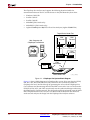
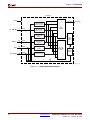
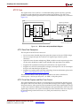
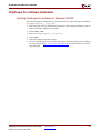
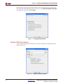
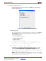
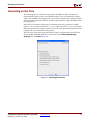
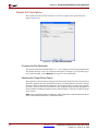
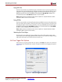
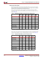
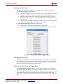
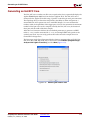
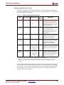
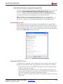
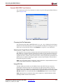
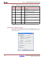
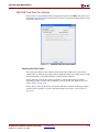
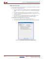
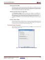
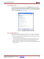
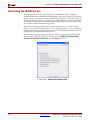
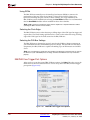
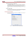
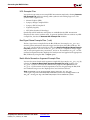
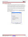
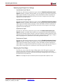
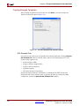
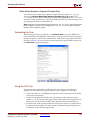
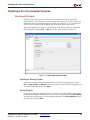
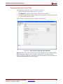
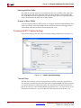
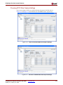
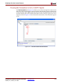
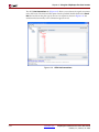
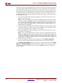
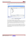
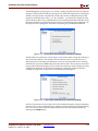
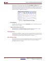
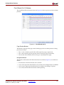
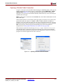
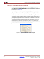
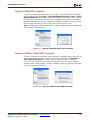
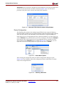
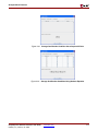
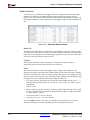
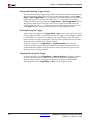
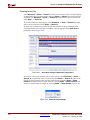
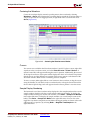
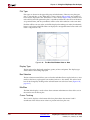
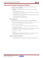
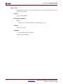
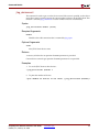
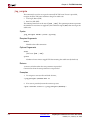
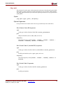
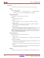
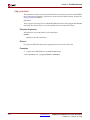
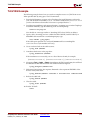
R
ChipScope Pro Core Inserter Features
Specifying Input and Output Files
The ChipScope Core Inserter works in a step-by-step process.
1.
Specify the Input Design Netlist (Figure 3-3, page 3-5).
2.
Click Browse to navigate to the directory where the netlist resides.
3.
Modify the Output Design Netlist and Output Directory fields as needed. (These fields
are automatically filled in initially.)
Figure 3-4 shows a project with input and output files specified.
Figure 3-4:
Core Inserter Project with Files Specified
Note: When the Core Inserter is invoked from the Project Navigator tool, the Input Design Netlist,
Output Design Netlist, Output Directory and Device Family fields are automatically filled in
(Figure 3-5, page 3-8). In this case, these fields can only be changed by the Project Navigator tool
and cannot be modified directly in the Core Inserter.
ChipScope Pro Software and Cores User Guide
UG029 (v7.1) February 16, 2005
www.xilinx.com
3-7
R
Chapter 3: Using the ChipScope Pro Core Inserter
Figure 3-5: Core Inserter as Launched from Project Navigator
Project Level Parameters
Three project level parameters (device family, SRL16 usage, and RPM usage) must be
specified for every project. Due to the increased depth of Virtex-II device block RAM,
different cores can be generated to take advantage of these deeper RAMs.
Selecting the Target Device Family
The target FPGA device family is displayed in the Device Family field. The structure of the
ICON and capture cores are optimized for the selected device family. Use the pull-down
selection to change the device family to the desired architecture.
The default target device family is Virtex-II.
Using SRL16s
The Use SRL16s checkbox is used to select whether or not the cores will be generated
using SRL16 and SRL16E components. This option is only available for the Virtex-II,
Virtex-II Pro, Virtex-4, Spartan-3, and Spartan-3E device families (including the QPro
variants of these families). If the checkbox is not selected, the SRL16 components are
replaced with flip-flops and multiplexers, which affects the size and performance of the
generated cores.
The Use SRL16s checkbox is checked by default to generate cores that use the optimized
SRL16 technology.
3-8
www.xilinx.com
ChipScope Pro Software and Cores User Guide
UG029 (v7.1) February 16, 2005
R
ChipScope Pro Core Inserter Features
Using RPMs
The Use RPMs checkbox is used to select whether the individual cores should be
relationally placed macros (RPMs). This option places restraints on the place-and-route tool
to optimize placement of all the logic for the ChipScope Pro core in one area. If your design
uses most of the resources in the device, these placement constraints may not be met. The
Use RPMs checkbox is checked by default in order to generate cores that are optimized for
placement. When this step is completed, click Next.
Choosing ICON Options
The first options that need to be specified are for the ICON core. The ICON core is the
controller core that connects all ILA, ILA/ATC, and ATC2 cores to the JTAG boundary scan
chain. The ICON core has the parameters shown in Figure 3-6.
Disabling JTAG Clock BUFG Insertion
Disabling the JTAG clock BUFG insertion causes the implementation tools to route the
JTAG clock using normal routing resources instead of global clock routing resources. By
default, this clock is placed on a global clock resource (BUFG). To disable this BUFG
insertion, check the Disable JTAG Clock BUFG Insertion checkbox.
Note: This should only be done if global resources are very scarce; placing the JTAG clock on
regular routing, even high-speed backbone routing, introduces skew. Make sure the design is
adequately constrained to minimize this skew.
After selecting the desired ICON parameters (Figure 3-6) click Next or New ILA Unit to
automatically create an ILA core and display the Select Logic Analyzer Options window.
To add a new ATC2 core instead of an ILA core, click either New ATC2 Unit. To add a new
ILA/ATC core, select the Edit → New ILA/ATC Unit menu option.
Figure 3-6:
ChipScope Pro Software and Cores User Guide
UG029 (v7.1) February 16, 2005
www.xilinx.com
ICON Options
3-9
R
Chapter 3: Using the ChipScope Pro Core Inserter
Choosing ILA or ILA/ATC Trigger Options and Parameters
Notice in Figure 3-7 that a new ILA unit has been created in the device hierarchy on the
left. The next step is to set up the ILA unit. Figure 3-7 shows a sample of the first tab in the
ILA options and parameters sequence. The first tab sets up the trigger options for the ILA
or ILA/ATC core.
Figure 3-7:
ILA Core Trigger Parameters
Selecting the Number of Trigger Ports
Each ILA or ILA/ATC core can have up to 16 separate trigger ports that can be set up
independently. After you select the number of trigger ports from the Number of Trigger
Ports pull-down list, a group of options appears for each of these ports. The group of
options associated with each trigger port is labeled with TRIGn, where n is the trigger port
number 0 to 15. The trigger port options include trigger width, number of match units
connected to the trigger port, and the type of these match units.
Entering the Width of the Trigger Ports
The individual trigger ports are buses that are made up of individual signals or bits. The
number of bits used to compose a trigger port is called the trigger width. The width of each
trigger port can be set independently using the TRIGn Trigger Width field. The range of
values that can be used for trigger port widths is 1 to 256.
Selecting the Number of Trigger Match Units
A match unit is a comparator that is connected to a trigger port and is used to detect events
on that trigger port. The results of one or more match units are combined together to form
the overall trigger condition event that is used to control the capturing of data. Each trigger
port TRIGn can be connected to 1 to 16 match units by using the # Match Units pull-down
list.
3-10
www.xilinx.com
ChipScope Pro Software and Cores User Guide
UG029 (v7.1) February 16, 2005
R
ChipScope Pro Core Inserter Features
Selecting one match unit conserves resources while still allowing some flexibility in
detecting trigger events. Selecting two or more trigger match units allows a more flexible
trigger condition equation to be a combination of multiple match units. However,
increasing the number of match units per trigger port also increases the usage of logic
resources accordingly.
Note: The aggregate number of match units used in a single ILA core cannot exceed 16, regardless
of the number of trigger ports used.
Selecting the Match Unit Type
The different comparisons or match functions that can be performed by the trigger port
match units depend on the type of the match unit. Six types of match units are supported
by the ILA and ILA/ATC cores (Table 3-1).
Table 3-1: ILA Trigger Match Unit Types
Type
Bit Valuesa Match Function
Bits Per
Sliceb
Description
Basic
0, 1, X
‘=’, ‘<>’
8
Can be used for comparing data
signals where transition detection is
not important. This is the most bitwise economical type of match unit.
Basic
w/edges
0, 1, X, R, F, B
‘=’, ‘<>’
4
Can be used for comparing control
signals where transition detection
(e.g., low-to-high, high-to-low, etc.)
is important.
Extended
0, 1, X
‘=’, ‘<>’, ‘>’, ‘>=’,
‘<‘, ‘<=’
2
Can be used for comparing address
or data signals where magnitude is
important.
Extended
w/edges
0, 1, X, R, F, B
‘=’, ‘<>’, ‘>’, ‘>=’,
‘<‘, ‘<=’
2
Can be used for comparing address
or data signals where a magnitude
and transition detection are
important.
Range
0, 1, X
‘=’, ‘<>’, ‘>’, ‘>=’,
‘<‘, ‘<=’, ‘in
range’, ‘not in
range’
1
Can be used for comparing address
or data signals where a range of
values is important.
Range
w/edges
0, 1, X, R, F, B
‘=’, ‘<>’, ‘>’, ‘>=’,
‘<‘, ‘<=’, ‘in
range’, ‘not in
range’
1
Can be used for comparing address
or data signals where a range of
values and transition detection are
important.
a. Bit values: ‘0’ means “logical 0”, ‘1’ means “logical 1”, ‘X’ means “don’t care”, ‘R’ means “0-to-1
transition”, ‘F’ means “1-to-0 transition” and ‘B’ means “any transition”.
b. The Bits Per Slice value is only an approximation that is used to illustrate the relative resource
utilization of the different match unit types. It should not be used as a hard estimate of resource
utilization.
Use the TRIGn Match Type pull-down list to select the type of match unit that will apply to
all match units connected to the trigger port. However, as the functionality of the match
unit increases, so does the amount of resources necessary to implement that functionality.
This flexibility allows you to customize the functionality of the trigger module while
keeping resource usage in check.
ChipScope Pro Software and Cores User Guide
UG029 (v7.1) February 16, 2005
www.xilinx.com
3-11
R
Chapter 3: Using the ChipScope Pro Core Inserter
Selecting Match Unit Counter Width
The match unit counter is a configurable counter on the output of the each match unit in a
trigger port. This counter can be configured at run time to count a specific number of
match unit events. To include a match counter on each match unit in the trigger port, select
a counter width from 1 to 32. The match counter will not be included on each match unit if
the Counter Width combo box is set to Disabled. The default Counter Width setting is
Disabled.
Enabling the Trigger Condition Sequencer
The trigger condition sequencer is a standard Boolean equation trigger condition that can be
augmented with an optional trigger sequencer by checking the Enable Trigger
Sequencer checkbox. A block diagram of the trigger sequencer is shown in Figure 3-8.
Match Unit 0
Match Unit 0
Match Unit 1
Match Unit 1
Match Unit 2
Match Unit 15
Level
1
Match Unit 0
Match Unit 1
Level
2
Match Unit 2
Match Unit 15
Match Unit 2
Level
16
Trigger
Match Unit 15
UG029_trig_seq_blk_diag_081903
Figure 3-8:
Trigger Sequencer Block Diagram with 16 Levels and 16 Match Units
The trigger sequencer is implemented as a simple cyclical state machine and can transition
through up to 16 states or levels before the trigger condition is satisfied. The transition
from one level to the next is caused by an event on one of the match units that is connected
to the trigger sequencer. Any match unit can be selected at run time on a per level basis to
transition from one level to the next. The trigger sequencer can be configured at run time to
transition from one level to the next on either contiguous or non-contiguous sequences of
match function events.
Enabling the Storage Qualification Condition
In addition to the trigger condition, the ILA core can also implement a storage qualification
condition. The storage qualification condition is a Boolean combination of match function
events. These match function events are detected by the match unit comparators that are
subsequently attached to the trigger ports of the core. The storage qualification condition
differs from the trigger condition in that it evaluates trigger port match unit events to
decide whether or not to capture and store each individual data sample. The trigger and
storage qualification conditions can be used together to define when to start the capture
process and what data to capture. The storage qualification condition can be enabled by
checking the Enable Storage Qualification checkbox.
Note: The storage qualification condition is not available in the ILA/ATC core.
3-12
www.xilinx.com
ChipScope Pro Software and Cores User Guide
UG029 (v7.1) February 16, 2005
R
ChipScope Pro Core Inserter Features
Choosing ILA Core Capture Parameters
The second tab in the Core Inserter that is used to set up the of the capture parameters of
the ILA core (Figure 3-9). The capture parameters for ILA are different from ILA/ATC (see
Figure 3-11, page 3-16).
Figure 3-9: ILA Core Capture Parameters
ChipScope Pro Software and Cores User Guide
UG029 (v7.1) February 16, 2005
www.xilinx.com
3-13
R
Chapter 3: Using the ChipScope Pro Core Inserter
Selecting the Data Depth
The maximum number of data sample words that the ILA core can store in the sample
buffer is called the data depth. The data depth determines the number of data width bits
contributed by each block RAM unit used by the ILA unit.
For the Virtex-II, Virtex-II Pro, Virtex-4, Spartan-3, and Spartan-3E device families
(including the QPro variants of these families), you can set the data depth to one of six
values (Table 3-2).
Table 3-2: Maximum Data Widths for Virtex-II/-II Pro/-4, Spartan-3/-3E
Depth
512
Depth
1024
Depth
2048
Depth
4096
Depth
8192
Depth
16384
1 block RAM
31
15
7
3
1
--
2 block RAMs
63
31
15
7
3
1
4 block RAMs
127
63
31
15
7
3
8 block RAMs
255
127
63
31
15
7
16 block RAMs
--
255
127
63
31
15
32 block RAMs
--
--
255
127
63
31
64 block RAMs
--
--
--
255
127
63
128 block RAMs
--
--
--
--
255
127
256 block RAMs
--
--
--
--
--
255
Note: One extra bit per sample is required for the trigger mark (e.g., a trigger/data width of 7 bits
requires a full sample width of 8 bits, etc.)
For the Virtex, Virtex-E, Spartan-II and Spartan-IIE device families (including the QPro
variants of these families), you can set the data depth to one of five values (Table 3-3).
Table 3-3: Maximum Data Widths for Virtex/-E, Spartan-II /-IIE
Depth
256
Depth
512
Depth
1024
Depth
2048
Depth
4096
1 block RAM
15
7
3
1
--
2 block RAMs
31
15
7
3
1
4 block RAMs
63
31
15
7
3
8 block RAMs
127
63
31
15
7
16 block RAMs
255
127
63
31
15
32 block RAMs
--
255
127
63
31
64 block RAMs
--
--
255
127
63
128 block RAMs
--
--
--
255
127
256 block RAMs
--
--
--
--
255
Note: One extra bit per sample is required for the trigger mark (e.g., a trigger/data
width of 7 bits requires a full sample width of 8 bits, etc.)
3-14
www.xilinx.com
ChipScope Pro Software and Cores User Guide
UG029 (v7.1) February 16, 2005
R
ChipScope Pro Core Inserter Features
Selecting the Data Type
The data captured by the ILA trigger port can come from two source types:
•
•
Data Separate from Trigger (Figure 3-9, page 3-13)
♦
The data port is completely independent of the trigger ports
♦
This mode is useful when you want to limit the amount of data being captured
Data Same as Trigger (Figure 3-10)
♦
The data and trigger ports are identical. This mode is very common in most logic
analyzers, since you can capture and collect any data that is used to trigger the
core.
♦
Individual trigger ports can be selected to be included in the data port. If this
selection is made, then the DATA input port will not be included in the port map
of the ILA core.
♦
This mode conserves CLB and routing resources in the ILA core, but is limited to
a maximum aggregate data sample word width of 256 bits.
Figure 3-10: ILA Core Data Same As Trigger Parameters
Selecting the Data-Same-As-Trigger Ports
If the Data Same As Trigger checkbox is selected, then a checkbox for each TRIGn port
appears in the data options screen. These checkboxes should be used to select the
individual trigger ports that will be included in the aggregate data port. Note that selecting
the individual trigger ports automatically updates the Aggregate Data Width field
accordingly. A maximum data width of 256 bits applies to the aggregate selection of trigger
ports.
ChipScope Pro Software and Cores User Guide
UG029 (v7.1) February 16, 2005
www.xilinx.com
3-15
R
Chapter 3: Using the ChipScope Pro Core Inserter
Entering the Data Width
The width of each data sample word stored by the ILA core is called the data width. If the
data and trigger words are independent from each other, then the maximum allowable
data width depends on the target device type and data depth. However, regardless of these
factors, the maximum allowable data width is 256 bits.
Number of Block RAMs
As the data depth and data width selections are changed, the Number of Block RAMs field
notifies you of how many block RAMs will be used by the ILA core. The trigger mark is
automatically taken into account when calculating this value.
Choosing ILA/ATC Capture Settings
If you are inserting an ILA/ATC core, the Capture Settings look like those in Figure 3-11.
Figure 3-11: ILA/ATC Core Data Settings
Transmit Rate
The ILA/ATC core does not use on-chip memory resources to store the captured trace
data. Instead, it transmits the data to be captured to an Agilent E5904B TPA that is attached
to a special connector via FPGA device pins. The data can be transmitted out the device
pins at the same rate as the incoming DATA port (transmit rate = 1x), twice the rate as the
DATA port (transmit rate = 2x) or four times the DATA port rate (transmit rate = 4x).
3-16
www.xilinx.com
ChipScope Pro Software and Cores User Guide
UG029 (v7.1) February 16, 2005
R
ChipScope Pro Core Inserter Features
Maximum CLK Port Frequency
The maximum output clock frequency is 200 MHz. The incoming CLK port rate is limited
by the maximum output clock frequency as well as the transmit rate. If the transmit rate is
1x, then the maximum CLK port frequency is 200 MHz. If the transmit rate is 2x, then the
maximum CLK port frequency is 100 MHz. Finally, if the transmit rate is 4x, then the
maximum CLK port frequency is 50 MHz.
Clock Resource Usage
The ILA/ATC core will use dedicated clock resources if the transmit rate is 2x or 4x. The
number of clock resources required by the ILA/ATC core are shown in Table 3-4.
Table 3-4: ILA/ATC Clock Resource Utilization
Virtex, Virtex-E,
Spartan-II and Spartan-IIE
Transmit
Rate
Virtex-II, Virtex-II Pro, Virtex-4,
Spartan-3, and Spartan-3E
Number of
BUFGs
Number of
CLKDLLs
Number of BUFGs
Number of DCMs
1x
0
0
0
0
2x
1
1
1
1
4x
1
2
2
1
Output Buffer Type
You can select the type of output buffer used for the output clock and data pins. The types
of output data buffers that are supported by the ILA/ATC cores depend on the device
family (Table 3-5).
Table 3-5: ILA/ATC Output Buffer Types by Device Family
Buffer Type
Virtex-II,
Virtex-II Pro,
Virtex-4,
Spartan-3,
Spartan-3E
Virtex-E,
Spartan-IIE
Virtex,
Spartan-II
LVTTL 3.3V 24mA Fast
Yes
Yes
Yes
LVTTL 3.3V 12mA Fast
Yes
Yes
Yes
LVCMOS 3.3V 24mA Fast
Yes
No
No
LVCMOS 3.3V 12mA Fast
Yes
No
No
LVCMOS 2.5V 24mA Fast
Yes
No
No
LVCMOS 2.5V 12mA Fast
Yes
Yes
Yes
LVCMOS 1.8V 16mA Fast
Yes
No
No
LVCMOS 1.8V 12mA Fast
Yes
Yes
No
LVDCI 3.3V
Yes
No
No
LVDCI 2.5V
Yes
No
No
LVDCI 1.8V
Yes
No
No
ChipScope Pro Software and Cores User Guide
UG029 (v7.1) February 16, 2005
www.xilinx.com
3-17
R
Chapter 3: Using the ChipScope Pro Core Inserter
Number of Data Pins
The ILA/ATC core can use 4, 8, 12, 16, or 20 output data pins for external capture.
Output Clock and Data Pin Locations
The clock and data pins are instantiated inside the ILA/ATC core for your convenience.
This means that although you do not have to manually bring the clock and data pins
through every level of hierarchy to the top-level of your design, you do need to specify the
location of these pins in the Core Generator. The pin locations are then added to the *.ncf
file of the ILA/ATC core.
Data Width and Depth
The data width and depth of the ILA/ATC core depend on the transmit rate and the
number of data pins (Table 3-6).
Table 3-6: ILA/ATC Core Capabilities
Number of Transmit
Data Pins
Rate
3-18
Max Width of
DATA Port
Max DATA Depth
(with timestamps)
4
1x
3
2,097,120 (1,048,560)
4
2x
5
1,048,560 (1048560)
4
4x
11
524,280 (262,136)
8
1x
7
2,097,120 (1,048,560)
8
2x
13
1,048,560 (524,280)
8
4x
27
524,280 (262,136)
12
1x
11
2,097,120 (1,048,560)
12
2x
21
1,048,560 (524,280)
12
4x
43
524,280 (262,136)
16
1x
15
2,097,120 (1,048,560)
16
2x
29
1,048,560 (524,280)
16
4x
59
524,280 (262,136)
20
1x
19
2,097,120 (1,048,560)
20
2x
37
1,048,560 (524,280)
20
4x
75
524,280 (262,136)
www.xilinx.com
ChipScope Pro Software and Cores User Guide
UG029 (v7.1) February 16, 2005
R
ChipScope Pro Core Inserter Features
Choosing ATC2 Data Capture Settings
If you are inserting an ATC2 core, the Pin Selection Parameters look like those in
Figure 3-12 and Figure 3-13 (for STATE mode and TIMING mode, respectively).
Figure 3-12: ATC2 Core STATE Mode Data Capture Settings
Figure 3-13: ATC2 Core TIMING Mode Data Capture Settings
ChipScope Pro Software and Cores User Guide
UG029 (v7.1) February 16, 2005
www.xilinx.com
3-19
R
Chapter 3: Using the ChipScope Pro Core Inserter
Capture Mode
The Capture Mode setting of the ATC2 core can be set to either STATE mode (Figure 3-12,
page 3-19) for synchronous data capture to the CLK input signal or to TIMING mode
(Figure 3-13, page 3-19) for asynchronous data capture. In STATE mode, the data path
through the ATC2 core uses pipeline flip-flops that are clocked on the CLK input port
signal. In TIMING mode, the data path through the ATC2 core is composed purely of
combinational logic all the way to the output pins. Also, in TIMING mode, the ATCK pin
is used as an extra data pin.
Clock Edge
The ATC2 unit can use either the rising or falling edges of the CLK signal to capture data
and run the internal calibration logic. The Clock Edge pull-down list is used to select either
the rising or falling edge of the CLK signal as the clock source for the ATC2 core.
Max Frequency Range
The Max Frequency Range parameter is used to specify the maximum frequency range in
which you expect to operate the ATC2 core. The implementation of the ATC2 core will be
optimized for the maximum frequency range selection. The valid maximum frequency
ranges are 0-100 MHz, 101-250 MHz, 251-300 MHz, and 301-500 MHz. The maximum
frequency range selection only has an affect on core implementation when the Capture
Mode is set to STATE mode.
Enable Auto Setup
The Enable Auto Setup option is used to enable a feature that allows the Agilent Logic
Analyzer to automatically set up the appropriate ATC2 pin to Logic Analyzer pod
connections. This feature also allows the Agilent Logic Analyzer to automatically
determine the optimal phase and voltage sampling offsets for each ATC2 pin. This feature
is enabled by default.
Enable "Always On" Mode
The Enable "Always On" Mode option is used to force an ATC2 core to always enable its
internal logic and output buffers. The "Always On" mode will also force the selection of
signal bank 0 upon FPGA device configuration. This mode makes it possible to capture
events that immediately follow device configuration without having to first set up the
ATC2 core manually. This feature is disabled by default and is only available when the
capture mode is set to TIMING mode.
Pin Edit Mode
The Pin Edit Mode parameter is a time saving feature that allows you to change the IO
Standard, Drive, and Slew Rate pin parameters on individual pins or together as a group of
pins. Setting the Pin Edit Mode to Individual allows you to edit the parameters of each pin
independently from one another. Setting the mode to Same as ATCK will allow you to
change the ATCK pin parameters and will force all ATD pins to the same settings. You
need to set unique pin locations for each individual pin regardless of the Pin Edit Mode.
ATD Pin Count
The ATC2 core can implement any number of ATD output pins in the range of 4 through
128.
3-20
www.xilinx.com
ChipScope Pro Software and Cores User Guide
UG029 (v7.1) February 16, 2005
R
ChipScope Pro Core Inserter Features
Endpoint Type
The Endpoint Type setting is used to control whether single-ended or differential output
drivers are used on the ATCK and ATD output pins. All ATCK and ATD pins must use the
same driver endpoint type.
Signal Bank Count
The ATC2 core contains an internal, run-time selectable data signal bank multiplexer. The
Signal Bank Count setting is used to denote the number of data input ports or signal banks
the multiplexer will implement. The valid Signal Bank Count values are 1, 2, 4, 8, 16, 32, or
64.
TDM Rate
The time division multiplexing (TDM) rate is used to increase the amount of data transmitted
over each data pin by as much as 200 percent. The ATC2 core does not use on-chip memory
resources to store the captured trace data. Instead, it transmits the data to be captured by
an Agilent logic analyzer that is attached to the FPGA pins using a special probe connector.
The data can be transmitted out the device pins at the same rate as the incoming DATA
port (TDM rate = 1x) or twice the rate as the DATA port (TDM rate = 2x). The TDM rate can
be set to “2x” only when the capture mode is set to “State”.
Data Width
The width of each input data port of the ATC2 core depends on the capture mode and the
TDM rate. In STATE mode, the width of each data port is equal to (ATD pin count) * (TDM
rate). In TIMING mode, the width of each data port is equal to (ATD pin count + 1) * (TDM
rate) since the ATCK pin is used as an extra data pin.
Pin Parameters
The settings in the Individual Pin Settings table control the location, I/O standard, output
drive and slew rate of each individual ATCK and ATD pin. The output clock (ATCK) and
data (ATD) pins are instantiated inside the ATC2 core for your convenience. This means
that although you do not have to manually bring the ATCK and ATD pins through every
level of hierarchy to the top-level of your design, you do need to specify the location and
other characteristics of these pins in the Core Generator. These pin attributes are then
added to the *.ncf file of the ATC2 core.
Pin Name
The ATC2 core has two types of output pins: ATCK and ATD. The ATCK pin is used as a
clock pin when the capture mode is set to STATE and is used as a data pin when the
capture mode is set to TIMING. The ATD pins are always used as data pins. The names of
the pins cannot be changed.
Pin Loc
The Pin Loc column is used to set the location of the ATCK or ATD pin.
ChipScope Pro Software and Cores User Guide
UG029 (v7.1) February 16, 2005
www.xilinx.com
3-21
R
Chapter 3: Using the ChipScope Pro Core Inserter
IO Standard
The IO Standard column is used to set the I/O standard of each individual ATCK or ATD
pin. The I/O standards that are available for selection depend on the device family and
driver endpoint type. The names of the I/O standards are the same as those in the
IOSTANDARD section of the Constraints Guide
(http://toolbox.xilinx.com/docsan/xilinx6/books/docs/cgd/cgd.pdf) in the Xilinx ISE 6
Software Manuals and Help - PDF Collection.
VCCO
The VCCO column setting denotes the output voltage of the pin driver and depends on the
IO Standard selection.
Drive
The Drive column setting denotes the maximum output current drive of the pin driver and
ranges from 2 to 24 mA, depending on the IO Standard selection.
Slew Rate
The Slew Rate column can be set to either FAST or SLOW for each individual ATCK or
ATD pin.
Core Utilization
The ATC2 core generator has a core resource utilization monitor that estimates the number
of look-up tables (LUTs) and flip-flops (FF) used by the ATC2 core, depending on the
parameters used. The ATC2 core never uses block RAM or additional clock resources (for
example, BUFG or DCM components).
3-22
www.xilinx.com
ChipScope Pro Software and Cores User Guide
UG029 (v7.1) February 16, 2005
R
ChipScope Pro Core Inserter Features
Choosing Net Connections for ILA or ILA/ATC Signals
The Net Connections tab (Figure 3-14) allows you to choose the signals to connect to the
ILA or ILA/ATC core. If trigger is separate from data, then the clock, trigger, and data ports
must be specified. When trigger equals data, only the clock and trigger/data ports must be
specified. Double-click on the CLOCK PORT label or click on the plus sign (+) next to it to
expand as shown in Figure 3-14. No connection has been made, so the connection appears
in red.
Figure 3-14: ILA and ILA/ATC Net Connections
ChipScope Pro Software and Cores User Guide
UG029 (v7.1) February 16, 2005
www.xilinx.com
3-23
R
Chapter 3: Using the ChipScope Pro Core Inserter
The ATC2 Net Connections tab (Figure 3-15) allows you to choose the signals to connect
to the ATC2 core. The clock and data ports must be specified. Double-click on the Clock
Net label or click on the plus sign (+) next to it to expand as shown in Figure 3-15. No
connection has been made, so the connection appears in red.
Figure 3-15:
3-24
www.xilinx.com
ATC2 Net Connections
ChipScope Pro Software and Cores User Guide
UG029 (v7.1) February 16, 2005
R
ChipScope Pro Core Inserter Features
To change any core connection, select Modify Connections. The Select Net dialog box now
appears (Figure 3-16).
Figure 3-16: Select Net Dialog Box
This dialog box provides an easy interface to choose nets to connect to the ILA, ILA/ATC
or ATC2 cores. The hierarchical structure of the design can be traversed using the
Structure/Nets pane on the upper left of the Select Net dialog box. All the design’s nets of
the selected structure hierarchy level appear in the table on the lower left pane of the Select
Net dialog box. The following net information is displayed in this table:
•
Net Name: The name of the net as it appears in the EDIF netlist. The net name may be
different than the corresponding signal name in the HDL source due to renaming and
other optimizations during synthesis.
•
Source Instance: The instance name of the lower-level hierarchical component from
which the net at the current level of hierarchy is driven. The source instance does not
necessarily describe the originating driver of the net.
•
Source Component: The type of the component described by the Source Instance.
•
Base Type: The type of the lowest level driving component of the net. The base type is
either a primitive or black box component.
All of the net identifiers described above can be filtered for key phrases using the Pattern
text box and Filter button. Also, nets can be sorted in ascending and descending order
based on the various net identifiers by selecting the appropriate net identifier button in the
column headers of the net selection table.
Note: The net names are sorted in alpha-numeric or “bus element” order whenever possible.
Common delimiters such as “[“, “(“, etc., are used to identify possible bus element nets.
ChipScope Pro Software and Cores User Guide
UG029 (v7.1) February 16, 2005
www.xilinx.com
3-25
R
Chapter 3: Using the ChipScope Pro Core Inserter
The tabs for clock, data, and trigger inputs of the ILA or ILA/ATC core appear in the pane
at the upper right of the Select Net dialog box. If you are selecting nets for an ATC2 core,
then only the Clock and Data input port categories will appear at the upper right of the
Select Net dialog box. If multiple trigger or data ports exist, there will be multiple sub-tabs
on the bottom of the Net Selections pane, respectively. Nets that are selected at a given
level of hierarchy can be connected to inputs of the ILA, ILA/ATC, or ATC2 capture cores
by following these steps:
1.
In the lower-left table of the Select Net dialog box, select the net(s) that you want to
connect to the capture core.
Note: You can select multiple nets to connect to an equivalent number of capture core input
connections. Hold down the Shift key and use the left mouse button to select contiguous nets.
Use a combination of the Ctrl key and left mouse button to select non-contiguous nets. You can
also connect a single net to multiple capture core input signals by selecting a single net and
multiple capture core port signals.
2.
In the upper-right tabbed panel of the Select Net dialog box, select the desired capture
core input category: Clock Signals, Trigger Signals (trigger port tab if applicable), Data
Signals (or Trigger/Data Signals, if trigger is same as data).
3.
In the right-hand table of capture core inputs, select the channel(s) that you want to
connect to the selected net(s).
Note: You can select multiple capture core inputs to connect to an equivalent number of nets.
Hold down the Shift key and use the left mouse button to select contiguous ILA core inputs. Use
a combination of the Ctrl key and left mouse button to select non-contiguous ILA core inputs. You
can also connect a single net to multiple capture core input signals by selecting a single net and
multiple capture core port signals.
4.
In the lower-right part of the Select Net dialog box, click the Make Connections
button to make a connection between the selected nets and capture core inputs.
Use the Remove Connections button to remove any existing connections. Use the Move
Nets Up and Move Nets Down buttons to reorder the position of any selected connection.
Once the desired net connections have been made, click OK to return to the main Core
Inserter window.
3-26
www.xilinx.com
ChipScope Pro Software and Cores User Guide
UG029 (v7.1) February 16, 2005
R
ChipScope Pro Core Inserter Features
All the trigger and data nets must be chosen in this fashion. After you have chosen all the
nets for a given bus, the ILA, ILA/ATC, or ATC2 bus name changes from red to black (see
Figure 3-17).
Figure 3-17: Specifying Data Connections
After specifying the clock, trigger, and data nets, click Next.
If you are using the Core Inserter in stand-along mode, a dialog box appears asking if you
want to proceed with Core Insertion. If Yes, the cores are generated, inserted into the
netlist, and an NGO file is created with the EDIF2NGD tool. Details of this process can be
viewed in the Messages pane at the bottom of the window. A Core Generation
Complete message in the Messages pane indicates successful insertion of ChipScope
cores.
If you are using the Core Inserter as part of the Project Navigator mode, a dialog box
appears asking if you want to return to Project Navigator. If Yes, the Core Inserter settings
are saved and you are returned to the Project Navigator tool. The actual core generation
and insertion processes take place in the proper sequence as deemed necessary by the
Project Navigator tool.
ChipScope Pro Software and Cores User Guide
UG029 (v7.1) February 16, 2005
www.xilinx.com
3-27
R
Chapter 3: Using the ChipScope Pro Core Inserter
Adding Units
Each device can support up to 15 ILA, ILA/ATC, or ATC2 units, depending on block RAM
availability and unit parameters.
•
To add another ILA unit to the project, select Edit → New ILA Unit, or go to the ICON
Options window by clicking on ICON in the tree on the left pane (Figure 3-6,
page 3-9) and clicking the New ILA Unit button.
•
To add another ILA/ATC unit to the project, select Edit → New ILA/ATC Unit, or go
to the ICON Options window by clicking on ICON in the tree on the left pane
(Figure 3-6, page 3-9) and clicking the New ILA/ATC Unit button.
•
To add another ATC2 unit to the project, select Edit → New ATC2 Unit, or go to the
ICON Options window by clicking on ICON in the tree on the left pane (Figure 3-6,
page 3-9) and clicking the New ATC2 Unit button.
You can set up the parameters for the additional units by using the same procedure as
described above.
Inserting Cores into Netlist
The core insertion step can be invoked by selecting the Insert → Insert Core menu option
or by clicking Insert Core on the toolbar.
Note: If you are using the ChipScope Pro Core Inserter flow in the Xilinx ISE 7.1i Project Navigator
tool, click Return to Project Navigator instead of selecting the Insert → Insert Core option.
The insertion of the cores will happen automatically as part of the Translate process in the Project
Navigator tool. Refer to Using the Core Inserter with ISE Project Navigator, page 3-1 for more details.
Managing Project Preferences
The preference settings are organized into three categories: Tools, ISE Integration, and
Miscellaneous. These preference settings are shown in Figure 3-18, Figure 3-19, page 3-29,
and Figure 3-20, page 3-29, respectively.
The Tools section (Figure 3-18) contains settings for the command line arguments used by
the Core Inserter to launch the EDIF2NGD tool.
Figure 3-18:
3-28
Core Inserter Tools Preference Settings
www.xilinx.com
ChipScope Pro Software and Cores User Guide
UG029 (v7.1) February 16, 2005
R
ChipScope Pro Core Inserter Features
The ISE Integration section (Figure 3-19) contains settings that affect how the Core Inserter
integrates with the Xilinx ISE Project Navigator tool. When ISE integration is enabled (the
default), the Core Inserter automatically searches the current working directory for ISE
temporary netlist directory called _ngo. If a valid ISE _ngo directory is found, the Core
Inserter project will be set up automatically to overwrite the intermediate NGD files of the
ISE project with those produced by the Core Inserter. The ISE Integration preferences can
be set by the user to prompt the user before overwriting any intermediate NGD files.
Figure 3-19:
Core Inserter ISE Integration Preference Settings
The Miscellaneous preferences section (Figure 3-20) contains other settings that affect how
the Core Inserter operates. For example, the Core Inserter can be set up by the user to
display the ports in the Select Net dialog box. This may be desired if the cores are being
inserted into a lower-level EDIF netlist, instead of the top level. These port nets are shown
in gray in the Select Net dialog box. The Core Inserter can also be set up to display nets that
are illegal for connection in the Select Net dialog box. When this preference option is
enabled, any illegal nets are shown in red in the Select Net dialog box.
Figure 3-20:
Core Inserter Miscellaneous Preference Settings
Also, the Core Inserter can be set up by the user to disable the display of source component
instance names, source component types, and base net driver types in the Select Net dialog
box. You can reset the Core Inserter project preferences to the installation defaults by
clicking on the Reset button.
ChipScope Pro Software and Cores User Guide
UG029 (v7.1) February 16, 2005
www.xilinx.com
3-29
R
3-30
Chapter 3: Using the ChipScope Pro Core Inserter
www.xilinx.com
ChipScope Pro Software and Cores User Guide
UG029 (v7.1) February 16, 2005
R
Chapter 4
Using the ChipScope Pro Analyzer
Analyzer Overview
The ChipScope Pro Analyzer tool interfaces directly to the ICON, ILA, ILA/ATC,
IBA/OPB, IBA/PLB, VIO, and ATC2 cores (collectively called the ChipScope Pro cores).
You can configure your device, choose triggers, setup the console, and view the results of
the capture on the fly. The data views and triggers can be manipulated in many ways,
providing an easy and intuitive interface to determine the functionality of the design.
Note: Even though the ChipScope Pro Analyzer tool will detect the presence of an ATC2 core, an
Agilent Logic Analyzer attached to a Xilinx JTAG cable is required to control and communicate with
the ATC2 core.
The ChipScope Pro Analyzer tool is made up of two distinct applications: the server and the
client. The ChipScope Pro Analyzer server is a command line application that connects to
the JTAG chain of the target system using any of the supported JTAG download cables
shown in Table 4-1. The ChipScope Pro Analyzer client is a graphical user interface (GUI)
application that allows you to interact with the devices in the JTAG chain and the
ChipScope Pro cores that are found in those devices.
Table 4-1: Operating System Support for the ChipScope Pro Analyzer
Application
ChipScope Pro
Analyzer Server
Windows XP Pro or
Windows 2000 SP2
Solaris 2.8 (32-bit)
or
Solaris 2.9 (32-bit)
Red Hat Linux
Enterprise WS3.0
(32-bit)
Yes
No
Yes
(supported JTAG
cables: Platform
Cable USB, Parallel
Cable IV, Parallel
Cable III, and
MultiPRO)
(supported JTAG
cables: Platform
Cable USB, Parallel
Cable IV, Parallel
Cable III, MultiPRO,
MultiLINX, and
Agilent E5904B TPA)
ChipScope Pro
Analyzer Client
ChipScope Pro Software and Cores User Guide
UG029 (v7.1) February 16, 2005
Yes
Yes
Yes
(Local and Remote)
(Remote Only)
(Local and Remote)
www.xilinx.com
4-1
R
Chapter 4: Using the ChipScope Pro Analyzer
The ChipScope Pro Analyzer server and client can be running on the same machine (local
host mode) or on different machines (remote mode). Remote mode is useful in the
following situations:
•
You need to debug a system that is in a different location
•
You need to share a single system resource with other team members
•
You need to demonstrate a problem or feature to someone who is not at your location
Remote mode is available on all operating systems, as shown in Table 4-1, page 4-1.
Analyzer Server Interface
The ChipScope Pro Analyzer server command line application is available on Windows
and Linux operating systems, as shown in Table 4-1, page 4-1. If you desire to debug a
target system that is connected directly to your local machine via a JTAG download cable,
then you do not need to start the server manually. You only need to start the server
application manually when you desire to interact with the server from a remote client.
Note: The ChipScope Pro Analyzer server application can handle only one client connection at a
time.
The server can be started as follows:
•
The ChipScope Pro Analyzer server is started on Windows machines by executing
$CHIPSCOPE/cs_server.bat <command line options>
•
The ChipScope Pro Analyzer server is started on Linux machines by executing
$CHIPSCOPE/bin/lin/cs_server.sh <command line options>
where the $CHIPSCOPE environment variable points to the ChipScope Pro 7.1i installation
directory. The ChipScope Pro Analyzer server application has several <command line
options> that are described in Table 4-2. You can customize the server scripts as needed.
Table 4-2: ChipScope Pro Analyzer Server Command Line Options
Command Line Option
Description
-port <portnumber>
Used to specify the TCP/IP port number that is used by the
client and server to establish a connection. The default port
number is 50001.
-password <password>
Used to protect the server from unauthorized access. No
password is set by default.
-l <logfile>
Used to specify the location of the log file. The default log file
location is:
$HOME/.chipscope/cs_analyzer_<portnumber>.log
where $HOME is the users home directory and
<portnumber> is the TCP/IP port number used by the
server.
Refer to the section Setting up a Server Host Connection, page 4-16 for more information
on how to connect to the server application from the ChipScope Pro Analyzer client
application.
4-2
www.xilinx.com
ChipScope Pro Software and Cores User Guide
UG029 (v7.1) February 16, 2005
R
Analyzer Client Interface
The ChipScope Pro Analyzer client interface consists of four parts:
•
Project tree in the upper part of the split pane on the left side of the window
•
Signal browser in the lower part of the split pane on the left side of the window
•
Message pane at the bottom of the window
•
Main window area
Both the project tree/signal browser split pane and the Message pane can be hidden by
deselecting those options in the View menu. Additionally, the size of each pane can be
adjusted by dragging the bar located between the panes to a new location. Each pane can
be maximized or minimized by clicking on the arrow buttons on the pane separator bars.
Project Tree
The project tree is a graphical representation of the JTAG chain and the ChipScope Pro
cores in the devices in the chain. Although all devices in the chain are displayed in the tree,
only valid target devices (Virtex, Virtex-E, Virtex-II, Virtex-II Pro, Virtex-4, Spartan-II,
Spartan-IIE, Spartan-3, Spartan-3E, and their QPro variants) can contain ChipScope Pro
cores and be operated upon. Leaf nodes in the tree appear when further operations are
available.
For instance, a leaf node for each ChipScope Pro unit appears when that device is
configured with a ChipScope Pro core-enabled bitstream. Context-sensitive menus are
available for each level of hierarchy in the tree. To access the context-sensitive menu, rightclick on the node in the tree. Device and unit renaming, child window opening, device
configuration, and project operations can all be done through these menus.
To rename a device or core unit node in the project tree, right-click on the node and select
Rename. To end the editing, press Enter or the up or down arrow key, or click on another
node in the tree.
Signal Browser
The signal browser displays all the signals for the core selected in the project tree. Signals
can be renamed, grouped into buses, and added to the various data views using contextsensitive menus in the signal browser.
Renaming Signals Buses, and Triggers Ports
To rename a signal, bus, or trigger port name in the signal browser, double click on it, or
right-click and select Rename. To end the editing, press Enter or the up or down arrow
key, or click on another node in the tree.
ChipScope Pro Software and Cores User Guide
UG029 (v7.1) February 16, 2005
www.xilinx.com
4-3
R
Chapter 4: Using the ChipScope Pro Analyzer
Adding/Removing Signals from Views
To remove all the signals from either the waveform or listing view, right-click on any data
signal or bus in the signal browser and select Clear All → Waveform or Clear All →
Listing. In the case of a VIO core, to remove all the signals from the VIO console, right-click
on any signal or bus, and select Clear All → Console. Similarly, all signals and buses can
be added to the views through the Add All to View menu options. Selected signals and
buses can be added through the Add to View menu options.
To select a contiguous group of signals and buses, click on the first signal, hold down the
Shift key, and click on the last signal in the group. To select a non-contiguous group of
signals and buses, click on each of the signals/buses in turn while holding down the Ctrl
key. When you use this method, the order of the signals in the bus are in the order in which
you select them.
Combining and Adding Signals Into Buses
For ILA and IBA cores, only data signals can be combined into buses. For VIO cores,
signals of a particular type can be grouped together to form buses. To combine signals into
buses, select the signals using the Shift or Ctrl keys as described above. When the Shift key
is used, the uppermost signal in the tree will be the LSB once the bus is created. If the Ctrl
key is used, the signals will be in ordered in the bus the same order that they are clicked,
the first signal being the LSB.
After you have selected the signals, right click on any selected signal and select Add to
Bus → New Bus. A new bus will be created at the top of the Data Signals and Buses
sub-tree (in the case of ILA and IBA cores), or at the top of that particular sub-tree (in the
case of VIO). To add a signal or signals into an existing bus, select the signals and select
Add to Bus, and then the bus name in the following submenu. Added signals always go
on the MSB-end of the bus.
Reverse Bus Ordering
To reverse the order of the bits in a bus (i.e. make the LSB the MSB), right click on the bus
and select Reverse Bus Order. The signal browser and all data views that contain that bus
will be immediately updated, and the bus values recalculated.
4-4
www.xilinx.com
ChipScope Pro Software and Cores User Guide
UG029 (v7.1) February 16, 2005
R
Analyzer Client Interface
Bus Radices
Each bus can be displayed in the data views in any one of the following radices:
•
ASCII
•
Binary
•
Hexadecimal
•
Octal
•
Signed decimal
•
Token
•
Unsigned decimal
ASCII is only available if the number of bits in the bus is evenly divisible by 8. Changing
the radix will change the bus radix in every data view it is resident.
Signed and Unsigned
When either signed or unsigned is chosen as a bus radix, a small dialog box appears for you
to enter three additional parameters: scale factor, offset and precision.
•
Scale factor is a multiplier value to use when calculating bus values. For instance, if the LSB of a
4-bit bus is 0010, and the scale factor is set to 2.0, the actual displayed bus value will be 4 (given
a precision of 0). If the scale factor is set to 0.1, then the actual displayed bus value will be 0.2
(given a precision of 1). The default scale factor is 1.0.
•
Offset is a constant value that will be added to the scaled bus value. The default offset is 0.
•
Precision is the number of decimal places to display after the decimal point. The default
precision is 0.
Token
Tokens are string labels that are defined in a separate ASCII file and can be assigned to a
particular bus value. These labels can be useful in applications such as address decoding
and state machines. The token file (.tok extension) has a very simple format, and can be
created or edited in any text editor. An example token file is provided in the token
directory in the ChipScope Pro install path (Figure 4-1).
Figure 4-1:
ChipScope Pro Software and Cores User Guide
UG029 (v7.1) February 16, 2005
www.xilinx.com
Example Token File
4-5
R
Chapter 4: Using the ChipScope Pro Analyzer
Tokens are chosen by selecting a bus, then choosing Bus Radix → Token from the
right-click menu. A dialog box opens and you can choose the token file. If the bus is wider
than the tokens specify (such as choosing 4-bit tokens for an 8-bit bus) the upper bits are
assumed 0 for the tokens to apply. Figure 4-2 shows such a waveform, with the example
token file in Figure 4-1 applied to an 8-bit bus.
Figure 4-2: Example Waveform with Tokens
Deleting Buses
To delete a bus, right click on it and select Delete Bus. The bus is immediately deleted in
every data view it is resident.
Type and Persistence (VIO only)
VIO signals have two additional properties: Type and Persistence. See VIO Bus/Signal
Activity Persistence, page 4-40 for explanations of these properties.
Message Pane
The Message pane displays a scroll list of status messages. Error messages appear in red.
The Message pane can be resized by dragging the split bar above it to a new location. This
also changes the height of the project tree/signal browser split pane.
Main Window Area
The main window area can display multiple child windows (such as Trigger, Waveform,
Listing, Plot windows) at the same time. Each window can be resized, minimized,
maximized, and moved as needed.
4-6
www.xilinx.com
ChipScope Pro Software and Cores User Guide
UG029 (v7.1) February 16, 2005
R
Analyzer Menu Features
Working with Projects
Projects hold important information about the ChipScope Pro Analyzer program state,
such as signal naming, signal ordering, bus configurations, and trigger conditions. They
allow you to conveniently store and retrieve this information between Analyzer sessions
When you first run the ChipScope Pro Analyzer tool, a new project is automatically created
and is titled new project. To open an existing project, select File → Open Project, or select
one of the recently used projects in the File menu. The title bar of the Analyzer and the
project tree displays the project name. If the new project is not saved during the course of
the session, a dialog box appears when the Analyzer is about to exit, asking you if you wish
to save the project.
Creating and Saving A New Project
To create a new project, select File → New Project. A new project called new project is
created and made active in the Analyzer. To save the new project under a different name,
select File → Save Project. The project file will have a .cpj extension.
Saving Projects
To rename the current project, or to save a copy to another filename, select File → Save
Project As (Figure 4-3), type the new name in the File name dialog box, and click Save.
Figure 4-3: Saving a Project
ChipScope Pro Software and Cores User Guide
UG029 (v7.1) February 16, 2005
www.xilinx.com
4-7
R
Chapter 4: Using the ChipScope Pro Analyzer
Printing Waveforms
One of the features of ChipScope Pro 7.1i is the ability to print a captured data waveform
(as shown in Figure 4-4) by using the File → Print menu option (as shown in Figure 4-5).
Selecting the File → Print menu option starts the Print Wizard.
Figure 4-4:
Example Waveform
Figure 4-5: Selecting the File → Print Option
The Print Wizard consists of three consecutive windows:
4-8
1.
(1 of 3) is the Print options and settings window (Figure 4-6, page 4-9)
2.
(2 of 3) is the Print waveform printout preview navigator window (Figure 4-8,
page 4-11)
3.
(3 of 3) is the Print confirmation window (Figure 4-11, page 4-13)
www.xilinx.com
ChipScope Pro Software and Cores User Guide
UG029 (v7.1) February 16, 2005
R
Analyzer Menu Features
Print Wizard (1 of 3) Window
The first Print Wizard window (shown in Figure 4-6) is used to set up various waveform
printing options. The following sections describe these waveform printing options in more
detail.
Figure 4-6:
Print Wizard (1 of 3)
Horizontal Scaling
You can control the amount of waveform data that prints to each column of pages using
one of two methods:
•
Fit To: Fit the waveform to one or more columns of pages
•
Fixed: Fit a specific number of waveform samples on each column of pages
The default fits the entire waveform printout to a single column of pages wide.
Signal/Bus Selection
You can control which signals and buses will be present in the waveform printout using
one of three methods:
•
Current View: Print waveform data for all of the signals and buses in the current view
of the waveform window
•
All: Print waveform data for all of the signals and buses available in the entire core
unit
•
Selected: Print waveform data for only those signals and buses that are currently
selected in the waveform window
The default prints waveform data using the Current View method.
ChipScope Pro Software and Cores User Guide
UG029 (v7.1) February 16, 2005
www.xilinx.com
4-9
R
Chapter 4: Using the ChipScope Pro Analyzer
Time/Sample Range
You can control the range of time units or number of samples printed using one of four
methods:
•
Current View: Print waveform data using the same range of samples that is present in
the current waveform view
•
Full Range: Print waveform data using a range of samples consisting of all samples in
the entire sample buffer
•
Between X/O Cursors: Print waveform data using a range of samples starting with the
X cursor and ending with the O cursor (or vice versa)
•
Custom View: Print waveform data using a range of samples defined by a starting
window and sample number and an ending window and sample number
The default prints waveform data using the Current View method.
Print Signal Names
You can choose to print the signal names (and X/O cursor values) on each page or only on
the first page. Printing the X/O cursor values on the first page only is useful when you
assemble multiple printed pages together to form a larger multi-dimensional plot.
X/O Cursor Values
You can also choose whether or not to include the X/O cursor values in the waveform
printout. If you choose to display the X/O cursor values in the waveform printout, then
they will either appear on each page or only on the first page, depending on the Print
Signal Names setting (see previous section “Print Signal Names”).
Footer
You can enable or disable the inclusion of a footer at the bottom of each page by selecting
the Show Footer checkbox. An example of the information that appears in the footer is
shown in Figure 4-7.
Figure 4-7: Waveform Printout Footer Example
Navigation Buttons
The buttons at the bottom of the Print Wizard (1 of 3) window (Figure 4-6, page 4-9) are
defined as follows:
•
Page Setup: Opens the page setup window (refer to Figure 4-12, page 4-13)
•
Next: Opens the Print Wizard (2 of 3) window
•
Cancel: Closes the Print Wizard window without printing
Clicking on the Next button takes you to the Print Wizard (2 of 3) window, described in
Print Wizard (2 of 3) Window, page 4-11.
4-10
www.xilinx.com
ChipScope Pro Software and Cores User Guide
UG029 (v7.1) February 16, 2005
R
Analyzer Menu Features
Print Wizard (2 of 3) Window
The second Print Wizard window (shown in Figure 4-8) shows a preview of the waveform
printout.
Figure 4-8:
Print Wizard (2 of 3)
Page Preview Buttons
The buttons at the top of the page control which page of the waveform printout is being
previewed as follow:
•
The << and >> buttons go to the first and last preview pages, respectively
•
The < and > buttons go to the previous and next preview pages, respectively
•
The text box in the middle can be used to go to a specific preview page
Navigation Buttons
The buttons at the bottom of the Print Wizard (2 of 3) window (Figure 4-8) are defined as
follows:
•
Back: Returns to the Print Wizard (1 of 3) window
•
Send to PDF: Opens the Print Wizard (3 of 3) window for writing directly to a PDF File
•
Send to Printer: Opens the Print Wizard (3 of 3) window for sending to a printer
•
Close: Closes the Print Wizard window without printing
ChipScope Pro Software and Cores User Guide
UG029 (v7.1) February 16, 2005
www.xilinx.com
4-11
R
Chapter 4: Using the ChipScope Pro Analyzer
Bus Expansion and Contraction
You can manipulate the waveform by expanding and contracting the buses in the print
preview window. For example, if you expand a bus in Figure 4-8, page 4-11 such that it
pushes other signals/buses to another page, the total print preview page count at the top
will change accordingly, as shown in Figure 4-9.
Figure 4-9: Expanding Buses in Print Wizard (2 of 3)
Print Wizard (3 of 3) Window
In the Print Wizard (2 of 3) window, clicking on the Send to PDF button goes to the Print
Wizard (3 of 3) PDF confirmation window (see Figure 4-10). Clicking on the Yes button
causes the waveform printout to be written to the specified PDF file while clicking on the
No button returns you to the Print Wizard (2 of 3) window. Clicking on Change File opens
a file browser window that allows you to select or create a new PDF file.
Figure 4-10: Print Wizard (3 of 3) for Sending to a PDF File
4-12
www.xilinx.com
ChipScope Pro Software and Cores User Guide
UG029 (v7.1) February 16, 2005
R
Analyzer Menu Features
In the Print Wizard (2 of 3) window, clicking on the Send to Printer button goes to the Print
Wizard (3 of 3) Printer confirmation window (see Figure 4-11). Clicking on the Yes button
causes the waveform printout to be sent to the printer while clicking on the No button
returns you to the Print Wizard (2 of 3) window.
Figure 4-11: Print Wizard (3 of 3) for Sending to a Printer
Page Setup
The Page Setup window (shown in Figure 4-12) can be invoked either from the Print
Wizard (1 of 3) window (Figure 4-6, page 4-9) or by using the File → Page Setup menu
option.
Note: In the ChipScope Pro 7.1i Analyzer program, you can print only to the default system printer.
Changing the target printer in the print setup window does not have any effect. To change printers,
you must close the Analyzer program, change your default system printer, and restart the Analyzer
program.
Figure 4-12: Page Setup Window
ChipScope Pro Software and Cores User Guide
UG029 (v7.1) February 16, 2005
www.xilinx.com
4-13
R
Chapter 4: Using the ChipScope Pro Analyzer
Importing Signal Names
At the start of a project, all of the signals in every ChipScope Pro core have generic names.
You can rename the signals individually as described in Renaming Signals Buses, and
Triggers Ports, page 4-3, or import a file that contains all the names of all the signals in one
or more cores. The ChipScope Pro Core Generator, ChipScope Pro Core Inserter, Synplicity
Certify, and the Xilinx FPGA Editor tools can create such files. To import signal names from
a file, select File → Import. A Signal Import dialog box will appear (Figure 4-13).
Figure 4-13:
Blank Signal Import Dialog Box
To select the signal import file, select Select New File. A file dialog box will appear for you
to navigate and specify the signal import file. After you choose the file, the Unit/Device
combo box will be populated, according to the core types specified in the signal import file.
If the signal import file contains signal names for more than one core, the combo box will
contain device numbers for all devices that contain only ChipScope Pro capture cores.
If the signal import file contains signal names for only one core, the combo box will be
populated with names of the individual cores that match the type specified in the signal
import file. If the import file is a file from Synplicity Certify, you will also have the option
of choosing a device name from the Certify file as well as the device in the JTAG chain.
To import the signal names, click OK. If the parameters in the file do not match the
parameters of the target core or cores, a warning message will be displayed. If you choose
to proceed, the signal names will be applied to the cores as applicable.
4-14
www.xilinx.com
ChipScope Pro Software and Cores User Guide
UG029 (v7.1) February 16, 2005
R
Analyzer Menu Features
Exporting Data
Captured data from an ILA or IBA core can be exported to a file, for future viewing or
processing. To export data, select File → Export. The Export Signals dialog box appears
(Figure 4-14).
Figure 4-14: Export Signals Dialog Box
Three formats are available: value change dump (VCD) format, tab-delimited ASCII format, or
the Agilent Technologies Fast Binary Data Format (FBDF). To select a format, click its radio
button. To select the target core to export, select it from the Core combo box.
Different sets of signals and buses are available for export. Use the Signals to Export combo
box to select:
•
All the signals and buses for that particular core, or
•
All the signals and buses present in the core’s waveform viewer, or
•
All the signals and buses in the core’s listing viewer, or
•
All the signals and buses in the core’s bus plot viewer
To export the signals, click Export. A file dialog box will appear from which you can
specify the target directory and filename.
Closing and Exiting the Analyzer
To exit the ChipScope Pro Analyzer, select File → Exit. The current active project is
automatically saved upon exit.
Viewing Options
The split pane on the left of the Analyzer window and the Message pane at the bottom of
the window can both be hidden or displayed per the user’s choice. Both are displayed the
first time the Analyzer is launched. To hide the project tree/signal browser split pane,
uncheck it under View → Project Tree. To hide the Message pane, uncheck it under
View → Messages.
ChipScope Pro Software and Cores User Guide
UG029 (v7.1) February 16, 2005
www.xilinx.com
4-15
R
Chapter 4: Using the ChipScope Pro Analyzer
Setting up a Server Host Connection
The ChipScope Pro Analyzer client GUI application requires a connection to the
ChipScope Pro Analyzer server application that is running on either the local or a remote
system. Select the JTAG Chain JTAG Chain→ Server Host Setting. This pops up the
server settings dialog shown in Figure 4-15.
Figure 4-15: Server Settings for Local Mode
For local mode operation, the server Host setting should always be set to localhost (as
shown in Figure 4-15). The Port setting can be set to any unused TCP/IP port number. The
default Port number is 50001. In local mode, the Password setting is not necessary in local
mode.
Note: In local mode, the server is started automatically.
Figure 4-16:
Server Settings for Remote Mode
For remote mode operation, the server Host setting should be set to an IP address or
appropriate system name (as shown in Figure 4-16). The Port and Password settings
should be set to the same port that was used when the server was started on the remote
system. In remote mode, the connection is not actually established until you open a
connection to a JTAG download cable, as described in the subsequent sections of this
document.
Note: In remote mode, the server needs to be started manually, as described in the section
Analyzer Server Interface, page 4-2.
4-16
www.xilinx.com
ChipScope Pro Software and Cores User Guide
UG029 (v7.1) February 16, 2005
R
Analyzer Menu Features
Opening a Parallel Cable Connection
To open a connection to the Parallel Cable (including the MultiPRO cable), make sure the
cable is connected to one of the computer’s parallel ports. Select JTAG Chain→ Xilinx
Parallel Cable (Figure 4-17). This pops up the Parallel Cable Selection configuration
dialog box. You can choose the Parallel Cable III, Parallel Cable IV, or have the Analyzer
autodetect the cable type.
Note: In order to open a connection to the MultiPRO cable, select either Parallel Cable IV or Auto
Detect Cable Type.
If the Parallel Cable IV or Auto Detect Cable Type option is selected, you can choose the
speed of the cable; the choices are 10 MHz, 5 MHz, 2.5 MHz (default), 1.25 MHz, or
625 kHz. Choose the speed that makes the most sense for the board under test. Type the
printer port name in the Port selection box (usually the default LPT1 is correct) and click
OK. If successful, the Analyzer queries the Boundary Scan chain to determine its
composition (see Setting Up the Boundary Scan (JTAG) Chain, page 4-20).
If the Analyzer returns the error message Failed to Open Communication Port,
verify that the cable is connected to the correct LPT port. If you have not installed the
Parallel Cable driver, follow the instructions in the ChipScope Pro Software installation
program to install the required device driver software.
Figure 4-17: Opening a Parallel Cable Connection
ChipScope Pro Software and Cores User Guide
UG029 (v7.1) February 16, 2005
www.xilinx.com
4-17
R
Chapter 4: Using the ChipScope Pro Analyzer
Opening an Agilent E5904B Cable Connection
To connect to the Agilent E5904B cable, make sure it has been properly configured
beforehand with a valid IP address, sub-net mask, gateway, etc. To open a connection,
select JTAG Chain → Agilent E5904B Cable. This will bring up the Agilent E5904B Cable
Options dialog box (Figure 4-18).
The Host/IP is the IP address of the cable. To properly configure the IP address of the
Agilent cable, please consult the Agilent E5904B option, FPGA 500 trace port analyzer
documentation.
The Connection Attempt Timeout text field indicates how long the ChipScope Analyzer
should attempt to communicate to the cable unsuccessfully before timing out.
The JTAG TCK Frequency combo box indicates the speed of the JTAG interface from the
Agilent cable to the JTAG chain. Choose a frequency that is appropriate for your system,
given signal integrity, and other concerns.
The JTAG Voltage Reference combo box indicates which voltage supply to use for the
communication to the JTAG chain: 3.3V internal, 2.5V internal, or an external supply.
The Trace Voltage Reference combo box indicates which voltage supply to use for the trace
port data pins: 3.3V internal, 2.5V internal, or an external supply.
Figure 4-18:
4-18
Agilent E5904B Cable Options Dialog Box
www.xilinx.com
ChipScope Pro Software and Cores User Guide
UG029 (v7.1) February 16, 2005
R
Analyzer Menu Features
Opening a MultiLINX connection
To connect to a MultiLINX cable, make sure the cable is properly connected to either the
serial or USB port and select Cable → Xilinx MultiLINX Serial Cable or Cable → Xilinx
MultiLINX USB Cable. If MultiLINX USB Cable is chosen, no other setup is necessary. The
ChipScope Analyzer will automatically query the USB ports and connect to the cable. If
MultiLINX Serial Cable is chosen, a configuration dialog box will open (Figure 4-19). Select
the correct port and baud rate. The default values will work in most cases.
Note: The ChipScope Pro Analyzer supports only the JTAG configuration mode for the MultiLINX
cable, regardless of port connection.
Figure 4-19: Opening a MultiLINX Serial Port Connection
Opening a Platform Cable USB Connection
To open a connection to the Parallel Cable (including the MultiPRO cable), make sure the
cable is connected to one of the computer’s parallel ports. Selecting the JTAG Chain→
Xilinx Platform USB Cable menu option pops up a dialog window, as shown in
Figure 4-20. You can choose the speed of the cable from any of the settings: 24 MHz,
12 MHz, 6 MHz, 3 MHz (default), 1.5 MHz, or 750 kHz. Choose the speed that makes the
most sense for the board under test.
Figure 4-20: Opening a Platform Cable USB Connection
ChipScope Pro Software and Cores User Guide
UG029 (v7.1) February 16, 2005
www.xilinx.com
4-19
R
Chapter 4: Using the ChipScope Pro Analyzer
Polling the Auto Core Status
When ChipScope Pro cores are armed, the interface cable will query the cores on a regular
basis to determine the status of the capture. If other programs are using the cable at the
same time as the ChipScope Pro Analyzer, it may be beneficial to turn this polling off. This
can be done in the JTAG Chain menu by un-checking JTAG Chain → Auto Core Status
Poll. If this option is unchecked, when the Run or Trigger Immediate operation is
performed, the Analyzer will not query the cores automatically to determine the status.
Note that this does not completely disable communication with the cable; it will only
disable the periodic polling when cores are armed. If one or more cores trigger after the
polling has been turned off, the capture buffer will not be downloaded from the device and
displayed in any of the data viewer(s) until the Auto Core Status Poll option is turned on
again.
Configuring the Target Device(s)
You can use the ChipScope Pro Analyzer software with one or more valid target devices.
The first step is to set up all of the devices in the Boundary Scan chain.
Setting Up the Boundary Scan (JTAG) Chain
After the Analyzer has successfully communicated with a download cable, it
automatically queries the Boundary Scan (JTAG) chain to find its composition. All Xilinx
Virtex/-E/-II/-II Pro/-4, Spartan-II/-IIE/-3/-3E,/XL, 9500/XL/XV, 4000XL/XLA, 18V00,
Platform FLASH PROMs, CoolRunner™, CoolRunner-II, and System ACE™ devices are
automatically detected. The entire IDCODE can be verified for valid target devices. To
view the chain composition, select JTAG Chain → JTAG Chain Setup. A dialog box
appears with all detected devices in order.
For devices that are not automatically detected, you must specify the IR (Instruction
Register) length to insure proper communication to the ChipScope Pro cores. This
information can be found in the device’s BSDL file. The following example has one System
ACE CompactFlash controller device (System_ACE), one serial PROMs (XC18V00™), and
one Virtex-II Pro device (XC2VP4™) in a chain (Figure 4-21). USERCODEs can be read out
of the ChipScope Pro target devices (only the XC2VP4 device in this example) by selecting
Read USERCODEs.
Figure 4-21:
Boundary Scan (JTAG) Setup Window
The ChipScope Pro Analyzer tool automatically keeps track of the test access port (TAP)
state of the devices in the JTAG chain, by default. If the ChipScope Pro Analyzer is used in
conjunction with other JTAG controllers (such as the System ACE CompactFlash (CF)
controller or processor debug tools), then the actual TAP state of the target devices can
differ from the tracking copy of the ChipScope Pro Analyzer. In this case, the ChipScope
Pro Analyzer should always put the TAP controllers into a known state (for example, the
Run-Test/Idle state) before starting any JTAG transaction sequences. Clicking on the
4-20
www.xilinx.com
ChipScope Pro Software and Cores User Guide
UG029 (v7.1) February 16, 2005
R
Analyzer Menu Features
Advanced button on the JTAG Chain Device Order dialog box reveals the parameters that
control the start and end states of JTAG transactions (Figure 4-22). Use the second
parameter if the JTAG chain is shared with other JTAG controllers.
Figure 4-22: Advanced JTAG Chain Parameters Setup Window
Device Configuration
The ChipScope Pro Analyzer can configure target FPGA devices using the following
download cables in JTAG mode only: Xilinx Platform Cable USB, Xilinx Parallel Cable III,
Xilinx Parallel Cable IV, Xilinx MultiPRO, Xilinx MultiLINX, or Agilent E5904B TPA.
If the target device is to be programmed using a download cable by way of the JTAG port,
select the Device menu, select the device you wish to configure, and select the Configure
menu option. Only valid target devices can be configured and are, therefore, the only
devices that have the Configure option available (Figure 4-23). Alternatively, you can
right-click on the device in the project tree to get the same menu as Device.
Figure 4-23: Device Menu Options
After selecting the configuration mode, the JTAG Configuration dialog box opens
(Figure 4-24). This dialog box reflects the configuration choice, and defaults to a blank
entry for the configuration file.
Figure 4-24: Selecting a Bitstream
ChipScope Pro Software and Cores User Guide
UG029 (v7.1) February 16, 2005
www.xilinx.com
4-21
R
Chapter 4: Using the ChipScope Pro Analyzer
To select the BIT file to download, click on Select New File. The Open Configuration File
dialog box (Figure 4-25) opens. Using the browser, select the device file you want to use to
configure the target device. It is important to select a BIT file generated with the proper
BitGen settings. Specifically, the -g StartupClk:JtagClk option must be used in BitGen in
order for configuration to be successful.
Once you locate and select the proper device file, click Open to return to the JTAG
Configuration dialog box (Figure 4-24).
Figure 4-25:
Opening a Configuration File
Once the BIT file has been chosen, click OK to configure the device.
Observing Configuration Progress
While the device is being configured, the status of the configuration is displayed at the
bottom of the Analyzer window. If the DONE status is not displayed, a dialog box opens,
explaining the problem encountered during configuration. If the download is successful,
the target device is automatically queried for ChipScope Pro cores, and the project tree is
updated with the number of cores present. A folder is created for each core unit found and
Trigger Setup, Waveform, and Listing leaf nodes appear under each ChipScope Pro unit.
A Bus Plot leaf node will appear only if the core unit is determined to be an ILA core.
Displaying JTAG User and ID Codes
One method of verifying that the target device was configured correctly is to upload the
device and user-defined ID codes from the target device. The user-defined ID code is the
8-digit hexadecimal code that can be set using the BitGen option -g UserID.
To upload and display the user-defined ID code for a particular device, select the Show
USERCODE option from the Device menu for a particular device (Figure 4-23, page 4-21).
Select the Show IDCODE option from the Device menu to display the fixed device ID code
for a particular device. The results of these queries are displayed in the Message window
4-22
www.xilinx.com
ChipScope Pro Software and Cores User Guide
UG029 (v7.1) February 16, 2005
R
Analyzer Menu Features
(Figure 4-26). The IDCODE and USERCODE can also be displayed in the JTAG Chain
Setup dialog box (JTAG Chain → JTAG Chain Setup, Figure 4-21, page 4-20).
Figure 4-26: Device USERCODE and IDCODE
Displaying Configuration Status Information
The 32-bit configuration status register contains information such as status of the
configuration pins and other internal signals. If configuration problems occur, select Show
Configuration Status from the Device menu for a particular target device to display this
information in the messages window (Figure 4-27).
Note: All target devices contain two internal registers that contain status information. These two
registers are the Configuration Status Register (32 bits) and the JTAG Instruction Register (variable
length, depending on the device). Only valid target devices have a Configuration Status Register.
Although all devices have a JTAG Instruction Register that can be read, whether any status
information is present depends on the implementation of that particular device. Refer to the data
sheet for a particular device for more information.
Figure 4-27: Displaying Device Configuration Status
For some devices, the JTAG instruction register contains status information as well. Use
Device → Show Instruction Register to display this information in the messages
window for any device in the JTAG chain (Figure 4-28).
Figure 4-28: Displaying Device Instruction Register Status
ChipScope Pro Software and Cores User Guide
UG029 (v7.1) February 16, 2005
www.xilinx.com
4-23
R
Chapter 4: Using the ChipScope Pro Analyzer
Trigger Setup Window
To set up the trigger for a ChipScope Pro ILA or IBA core, select Window → New Unit
Windows and the ChipScope Pro core desired(Figure 4-29). A dialog box will be displayed
for that ChipScope Pro core, and you can select the Trigger Setup, Waveform, Listing,
Bus Plot and/or Console window(s) in any combination (Figure 4-29). Windows cannot
be closed from this dialog box.
Figure 4-29: Opening New Unit Windows
The same operation can by achieved by double-clicking on the Trigger Setup leaf node in
the project tree, or by right-clicking on the Trigger Setup leaf node and selecting Open
Trigger Setup.
Each ChipScope Pro ILA, ILA/ATC, and IBA core has its own Trigger Setup window
which provides a graphical interface for the user to set up triggers. The trigger mechanism
inside each ChipScope Pro core can be modified at run-time without having to re-compile
the design. The following sections describe how to modify the trigger mechanism’s three
components:
•
Match Functions: Defines the match or comparison value for each match unit
•
Trigger Conditions: Defines the overall trigger condition based on a binary equation or
sequence of one or more match functions
•
Capture Settings: Defines how many samples to capture, how many capture windows,
and the position of the trigger in those windows
Each component is expandable and collapsible in the Trigger Setup window. To expand,
click on the desired button at the bottom of the window (Figure 4-30).
Figure 4-30: Trigger Setup Window with Only Match Functions Expanded
4-24
www.xilinx.com
ChipScope Pro Software and Cores User Guide
UG029 (v7.1) February 16, 2005
R
Analyzer Menu Features
To collapse, click on the button to the left of the expanded section you wish to collapse
(Figure 4-31).
Figure 4-31:
Trigger Setup Window with All Sections Expanded
Capture Settings
The capture settings section of the Trigger Setup window (Figure 4-32) defines the number
of windows, and where the trigger event occur in each of those windows. A window is a
contiguous sequence of samples containing one (and only one) trigger event. If an invalid
number is entered for any parameter, the text field turns red, and an error is displayed in
the Message pane.
Figure 4-32:
Capture Settings
Type
The Type combo box in the capture settings defines the type of windows to use. If Window
is selected, the number of samples in each window must be a power of two. However, the
trigger can be in any position in the window. If N Samples is selected, the buffer will have
as many windows as possible with the defined samples per trigger. The trigger will always
be the first sample in the window if N Samples is selected.
Windows
The Windows text field is only available when Window is selected in the Type combo box.
The number of windows is specified in this field and can be any positive integer from 1 to
the depth of the capture buffer.
ChipScope Pro Software and Cores User Guide
UG029 (v7.1) February 16, 2005
www.xilinx.com
4-25
R
Chapter 4: Using the ChipScope Pro Analyzer
Depth
The Depth combo box is only available when Window is selected in the Type combo box.
The Depth combo box defines the depth of each capture window. It is automatically
populated with valid selections when values are typed into the Windows text field. Only
powers of two are available.
Note: When the overall trigger condition consists of at least one match unit function that has a
counter that is set to either Occurring in at least n cycles or Lasting for at least n consecutive
cycles, the Window Depth or Samples Per Trigger setting cannot be less than eight samples. This is
due to the pipelined nature of the trigger logic inside the ILA, ILA/ATC, IBA/OPB and IBA/PLB cores.
Position
The Position text field is only available when Window is selected in the Type combo box.
The Position field defines the position of the trigger in each window. Valid values are
integers from 0 to the depth of the capture buffer minus 1.
Samples Per Trigger
The Sample Per Trigger text field is only available when N Samples is selected in the Type
combo box. Samples per trigger defines how many samples to capture once the trigger
condition occurs. Valid values are any positive integer from 1 to the depth of the capture
buffer. The trigger mark will always appear as sample 0 in the window. There will be as
many sample windows as possible captured, given the overall sample depth.
Note: When occurring in at least n cycles or occurring for at least n consecutive cycles is selected
for a match unit, and that match unit is a part of the overall trigger condition, the Window Depth or
Samples Per Trigger cannot be less than 8. This is due to pipeline effects inside the ILA, ILA/ATC, or
IBA core.
Timestamp
The Timestamp checkbox enables timestamps for capturing. This option is only enabled
for ILA/ATC cores. The timestamp value will appear in the horizontal ruler of the
Waveform and Listing windows.
Storage Qualification Condition
The storage qualification condition is a Boolean combination of events that are detected by the
match unit comparators that are subsequently attached to the trigger ports of the core. The
storage qualification condition evaluates trigger port match unit events to decide whether
or not to capture and store each individual data sample. The trigger and storage
qualification conditions can be used together to define when to start (or finish) the capture
process and what data is captured, respectively.
The Storage Condition dialog box has a table of all the match units. Each match unit
occupies a row in the table. The Enable column indicates if that match unit is part of the
trigger condition. The Negate column indicates if that match unit should be individually
negated (Boolean NOT) in the trigger condition.
The storage qualification condition can be configured to capture all data (as shown in
Figure 4-33, page 4-27), or it can be set up to capture data that satisfies a Boolean AND or
OR combination of all the enabled match units (as shown in Figure 4-34, page 4-27). The
overall Boolean equation can also be negated, selectable using the Negate Whole
Equation checkbox above the table. The resulting equation appears in the Storage
Condition Equation pane at the bottom of the window.
4-26
www.xilinx.com
ChipScope Pro Software and Cores User Guide
UG029 (v7.1) February 16, 2005
R
Analyzer Menu Features
Figure 4-33:
Figure 4-34:
ChipScope Pro Software and Cores User Guide
UG029 (v7.1) February 16, 2005
Storage Qualification Condition Set to Capture All Data
Storage Qualification Condition Using Boolean Equation
www.xilinx.com
4-27
R
Chapter 4: Using the ChipScope Pro Analyzer
Match Functions
A match function is a definition of a trigger value for a single match unit. All the match
functions are defined in the Match Functions section of the Trigger Setup window
(Figure 4-35). One or more match functions will be defined in an equation or sequence in
the Trigger Conditions section to specify the overall trigger condition of the ChipScope Pro
core.
Figure 4-35:
Setting the Match Functions
Match Unit
The Match Unit field indicates which match unit the function applies to. Clicking on the
+ symbol next to the match unit number (or double clicking on the field) will expand that
match unit so it is displayed as individual trigger port bits in at tree structure. Individual
values for each bit can then be viewed and set.
Function
The Function combo box selects which type of comparison is done. Only those
comparators that are allowed for that match unit are listed.
Value
The Value field selects exactly which trigger value to apply to that match unit. It is
displayed according to the Radix field. Double-clicking on the field will make it editable.
Place the cursor before the value you want to change, and typing a valid trigger character
will overwrite that character. Or, select the field by single-clicking, then proceed by typing
the trigger characters. Valid characters for the different radices are:
•
Hex: X, 0-9, and A-F. X indicates that all four bits of that nibble are don’t cares. A “?”
indicates that the nibble consists of a mixture of 1’s, 0’s, X’s, R’s, F’s, and B’s (where
appropriate)
•
Octal: X, ?, 0-7
•
Binary: X (don’t care), 0, 1, R (rising), F (falling), and B (either transition). R, F, and B
are only available if the match unit can detect transitions (Basic w/edges, Extended
w/edges, Range w/edges)
•
Unsigned: 0-9 (0 to 2n-1 for an n-bit bus)
•
Signed: 0-9 (-2n-1 to 2n-1 - 1 for an n-bit bus)
Also, when Bin is chosen as the radix, positioning the mouse pointer over a specific
character will display a tool-tip, indicating the name and position of that bit.
4-28
www.xilinx.com
ChipScope Pro Software and Cores User Guide
UG029 (v7.1) February 16, 2005
R
Analyzer Menu Features
Radix
The Radix combo box selects which radix to display in the Value field. Values are Hex,
Octal, Bin, Signed (not allowed for In Range and Out of Range comparisons), and
Unsigned.
Counter
The Counter field selects how many match function events must occur for the function to
be satisfied. If the match counter is present for a particular match unit, the text in the
Counter column will be in black text. If the counter is not present in the core, the text in that
column will be grayed out. To change the value of the match counter, click on the counter
cell, which will bring up the match unit counter dialog box (Figure 4-36).
Figure 4-36: Setting up the Match Counter
The Counter field selects how many match function events must occur for the function to
be satisfied.
•
If occurring in exactly n clock cycles is selected, then n contiguous or n noncontiguous
events will satisfy the match function counter condition.
•
If occurring in at least n clock cycles is selected, then n contiguous or n noncontiguous
events will satisfy the match function counter condition and will remain satisfied
until the overall trigger condition is met.
•
If occurring for at least n consecutive cycles is selected, then n contiguous events will
satisfy the match function counter condition and will remain satisfied until the overall
trigger condition is met or the match function value is no longer satisfied.
Note: When the overall trigger condition consists of at least one match unit function that has a
counter set to either Occurring in at least n cycles or Lasting for at least n consecutive cycles,
the Window Depth or Samples Per Trigger setting cannot be less than eight samples. This is due to
the pipelined nature of the trigger logic inside the ILA, ILA/ATC, IBA/OPB or IBA/PLB cores.
Trigger Conditions
A trigger condition is a Boolean equation or sequence of one or more match functions. The
ChipScope Pro core will capture data based on the trigger condition. More than one trigger
condition can be defined. To add a new trigger condition, click the Add button. To delete a
trigger condition, highlight any cell in the row and click Del. Although many trigger
conditions can be defined for a single core, only one trigger condition can be chosen
(active) at any one time.
Active
The Active field is a radio button that indicates which trigger condition is the currently
active one.
ChipScope Pro Software and Cores User Guide
UG029 (v7.1) February 16, 2005
www.xilinx.com
4-29
R
Chapter 4: Using the ChipScope Pro Analyzer
Trigger Condition Name Field
The Trigger Condition Name field provides a mnemonic for a particular trigger condition.
Trigger Condition n is used by default (Figure 4-37).
Figure 4-37:
Viewing the Trigger Condition
Trigger Condition Equation
The Condition Equation field displays the current Boolean equation or state sequence of
match functions that make up the overall trigger condition. By default, a logical AND of all
the match functions present (one match function for each match unit) is the trigger
condition. To change the trigger condition, click on the Condition Equation field, which
brings up the Trigger Condition dialog box.
Trigger Condition Editor Dialog Box
If a trigger sequencer is present in the core, the Trigger Condition dialog will have two tabs:
Boolean and Sequencer. When the Boolean tab is active, the trigger condition of a Boolean
equation of the available match units. When the sequencer tab is active, the trigger
condition is a state machine, where each state transition is triggered by a match function
being satisfied.
The Boolean tab of the Trigger Condition dialog box has a table of all the match units. Each
match unit occupies a row in the table. The Enable column indicates if that match unit is
part of the trigger condition. The Negate column indicates if that match unit should be
individually negated (Boolean NOT) in the trigger condition.
All the enabled match units can be combined in a Boolean AND or OR operation,
selectable using the radio buttons below the match unit table. The overall equation can also
be negated, selectable using the Negate checkbox below the table. The resulting equation
appears in the Trigger Condition Equation pane at the bottom of the window (Figure 4-38).
Figure 4-38: Setting the Trigger Condition Boolean Equation
4-30
www.xilinx.com
ChipScope Pro Software and Cores User Guide
UG029 (v7.1) February 16, 2005
R
Analyzer Menu Features
The Sequencer tab of the Trigger Condition dialog box has a combo box from which you
can select the number of levels in the trigger sequence and a table listing all the levels. The
sequencer begins at Level 1 and proceeds to Level 2 when the match unit specified in Level
1 has been satisfied. The number of levels available is a parameter of the core, up to a
maximum of 16 levels. Each level can look for a match unit being satisfied or not satisfied. To
negate a level (for instance, to look for the absence of a particular match function) check the
Negate cell for that level. A representation of the sequence appears in the Trigger
Condition Equation pane at the bottom of the window (Figure 4-39).
Figure 4-39:
Setting the Trigger Condition Sequencer
The trigger sequence in Figure 4-39 can be satisfied by the eventual occurrence of match
unit events M0 followed by M1 followed by M3 (with any occurrence or non-occurrence of
events in between). Enable the Use Contiguous Match Events Only checkbox if you
desire the trigger sequence to be satisfied only upon contiguous transitions from M0 to M1
to M3 (and not, for instance, the transitions of M0 followed by M1 followed by !M1
followed by M3).
Output Enable
If the trigger output is present in the core, a column named Output Enable becomes
available. This cell is a combo box that allows the user to select which type of signal will be
driven by the trig_out port of the ILA, ILA/ATC, or IBA core.
•
Disabled: The output is a constant 0.
•
Pulse (High): The output is a single clock cycle pulse of logic 1, 10 cycles after the
actual trigger event.
•
Pulse (Low): The output is a single clock cycle pulse of logic 0, 10 cycles after the actual
trigger event.
•
Level (High): The output transitions from a 0 to a 1 10 cycles after the actual trigger
event.
•
Level (Low): The output transitions from a 1 to 0 10 cycles after the actual trigger event.
ChipScope Pro Software and Cores User Guide
UG029 (v7.1) February 16, 2005
www.xilinx.com
4-31
R
Chapter 4: Using the ChipScope Pro Analyzer
Saving and Recalling Trigger Setups
All the information in the Trigger Setup window can be saved to a file for recall later with
the current project or other projects. To save the current trigger settings, select Trigger
Setup → Save Trigger Setup. A Save Trigger Setup As File dialog box will open, and the
trigger settings can be saved in any location, with a .ctj extension. To load a trigger
settings file into the current project, select Trigger Setup → Read Trigger Setup. A Read
Trigger Setup file dialog box will open, and you can navigate to the folder where the
trigger settings file (with a .ctj extension) exists. Once the trigger setting file is chosen,
select Open, and those settings will be loaded into the Trigger Settings window.
Running/Arming the Trigger
After setting up the trigger, select Trigger Setup → Run to arm it. The trigger stays armed
until the trigger condition is satisfied or you disarm the trigger. Once the trigger condition
is satisfied, the core captures data according to the capture settings. When the sample
buffer is full, the core stops capturing data. The data is then uploaded from the core and is
displayed in the Waveform and/or Listing windows.
To force the trigger, select Trigger Setup → Trigger Immediate. This causes the
ChipScope Pro unit to ignore the trigger condition and trigger immediately. After the
sample buffer fills with data, the trigger disarms and the captured data appears in the
Waveform and/or Listing window(s).
Stopping/Disarming the Trigger
To disarm the trigger, select TriggerSetup → Stop Acquisition. If the trigger condition
has been satisfied at least once before the acquisition is stopped, the ChipScope Pro
Analyzer program disarms the trigger and downloads/displays the captured data.
Subsequent selections of TriggerSetup → Run cause the trigger to re-arm.
4-32
www.xilinx.com
ChipScope Pro Software and Cores User Guide
UG029 (v7.1) February 16, 2005
R
Analyzer Menu Features
Waveform Window
To view the waveform for a particular ChipScope Pro ILA or IBA core, select Window →
New Unit Windows, and the ChipScope Pro core desired. A dialog box will be displayed
for that ChipScope Pro Unit, and the user can select the Trigger Setup, Waveform,
Listing, and/or Bus Plot window, or any combination. Windows cannot be closed from
this dialog box. The same operation can be achieved by double-clicking on the Waveform
leaf node in the project tree, or right-clicking on the Waveform leaf node and selecting
Open Waveform.
The Waveform window displays the sample buffer as a waveform display, similar to many
modern simulators and logic analyzers. All signal browser operations can also be
performed in the waveform window, such as bus creation, radix selection, renaming, etc.
To perform a signal operation, right-click on a signal or bus in the Bus/Signal column.
Bus and Signal Reordering
Buses and signals can be reordered in the Waveform window. Select one or more signals
and buses, and drag it to its new location. A ghost image of the signal or signals appears
with the cursor, and a red line shows the potential drop location..
Figure 4-40:
Reordering Buses or Signals in the Waveform
Cut/Copy/Paste/Delete Signals and Buses
Signals and buses can be cut, copied, pasted, or deleted using right-click menus. Select one
or more signals and/or buses, right click on a selected signal or bus, and select the
operation desired. Alternatively, the standard Windows key combinations are available
(Ctrl+X for cut, Ctrl+C for copy, Ctrl+V for paste, Del for delete).
ChipScope Pro Software and Cores User Guide
UG029 (v7.1) February 16, 2005
www.xilinx.com
4-33
R
Chapter 4: Using the ChipScope Pro Analyzer
Zooming In and Out
Select Waveform → Zoom → Zoom In to zoom in to the center of the waveform display,
or right-click in the waveform section and select Zoom → Zoom In. To zoom out from a
waveform, use Waveform → Zoom → Zoom Out, or right-click in the waveform and
select Zoom → Zoom Out.
To view the entire waveform display select Waveform → Zoom → Zoom Fit, or right
click in the waveform and select Zoom → Zoom Fit.
To zoom into a specific area, just use the left mouse button to drag a rectangle in the
waveform display. Once the drag is complete, a popup appears. Select Zoom Area to
perform the zoom (Figure 4-41).
Figure 4-41:
Zoom Area Using the Automatic Popup Menu
To zoom in to the space marked by the X and O cursors, select Waveform → Zoom →
Zoom X, O, or right-click in the waveform and select Zoom → Zoom X, O. Other zoom
features include zooming to the previous zoom factor by selecting Zoom → Zoom
Previous, zooming to the next zoom factor by selecting Zoom → Zoom Forward, and
zoom to a specific range of samples by selecting Zoom → Zoom Sample (Figure 4-42).
Figure 4-42: Zoom to Sample Range
4-34
www.xilinx.com
ChipScope Pro Software and Cores User Guide
UG029 (v7.1) February 16, 2005
R
Analyzer Menu Features
Centering the Waveform
Center the waveform display around a specific point in the waveform by selecting
Waveform → Go To, then centering the waveform display around the X and O markers, as
well as the previous or next trigger position, or right-click in the waveform and select
Go To (Figure 4-43).
Figure 4-43:
Centering the Waveform on a Marker
Cursors
Two cursors are available in the Waveform window: X and O. To place a cursor, right-click
anywhere in the waveform section, and select Place X Cursor or Place O Cursor. A
colored vertical line will appear indicating the cursor’s position. Additionally, the status of
all the signals and buses at that point will be displayed in the X or O column. The position
of both cursors, and the difference in position of the cursors appears at the bottom of the
Waveform window. Both cursors are initially placed at sample 0.
To move a cursor, either right-click in a new location in the waveform, or drag the cursor
using the handles (X or O labels) in the waveform header, or drag the cursor-line itself in
the waveform. Special drag icons will appear when the mouse pointer is over the cursor.
Sample Display Numbering
The horizontal axis of the waveform can be displayed as the sample number relative to the
sample window (default) or by the overall sample number in the buffer. To display the
sample number starting over at 0 for each window, select Ruler → Sample # in Window
in the right-click menu. To display the sample number as an overall sample count in the
buffer, select Ruler → Sample # in Buffer in the right-click menu. You can also select
toggle the way that the samples that occur before the trigger marker are shown in the ruler
(either negative or positive) by selecting Ruler → Negative Time/Samples in the
right-click menu.
ChipScope Pro Software and Cores User Guide
UG029 (v7.1) February 16, 2005
www.xilinx.com
4-35
R
Chapter 4: Using the ChipScope Pro Analyzer
Displaying Markers
A static red vertical bar is displayed at each trigger position. A static black bar is displayed
between two windows to indicate a period of time where no samples were captured. To not
display either of these markers, un-check them on the right-click menu under Markers →
Window Markers or Markers → Trigger Markers.
Listing Window
To view the Listing window for a particular ChipScope Pro ILA or IBA core, select Window
→ New Unit Windows, and the ChipScope Pro core desired. A dialog box will be
displayed for that ChipScope Pro Unit, and the user can select the Trigger Setup,
Waveform, Listing, and/or Bus Plot window, or any combination. Windows cannot be
closed from this dialog box. The same operation can be achieved by double-clicking on the
Listing leaf node in the project tree, or right-clicking on the Listing leaf node and selecting
Open Listing.
The Listing window displays the sample buffer as a list of values in a table. Individual
signals and buses are columns in the table (Figure 4-44). All signal browser operations can
also be performed in the listing window, such as bus creation, radix selection, and
renaming. To perform a signal operation, right-click on a signal or bus in the column
heading.
Figure 4-44:
The Listing View
Bus and Signal Reordering
Buses and signals can be reordered in the Listing window. Simply click on a signal or bus
heading in the table, and drag it to a new location.
Removing Signals/Buses
Individual signals and buses can be removed from the Listing window by right-clicking
anywhere in the signal’s column and selecting Remove. If Remove All is selected, all
signals and buses will be removed.
4-36
www.xilinx.com
ChipScope Pro Software and Cores User Guide
UG029 (v7.1) February 16, 2005
R
Analyzer Menu Features
Cursors
Cursors are available in the Listing window the same way as in the Waveform window. To
place a cursor, right-click in the data section of the Listing window, and select either Place
X Cursor or Place O Cursor. That line in the table will be colored the same as the cursor
color. To move the cursor to a different position in the table, either right-click in the new
location and do the same operation as before, or right-click on the cursor handle in the first
column, and drag it to the new location.
Goto Cursors
To automatically scroll the listing view to a cursor, right-click and select Go To → Go To X
Cursor or Go To → Go To O Cursor.
Bus Plot Window
To view the Bus Plot (1) window for a particular set of ILA or IBA buses, select Window →
New Unit Windows and the core desired. A dialog box will be displayed for that
ChipScope Pro Unit, and the user can select the Trigger Setup, Waveform, Listing, and /or
Bus Plot window, or any combination. Windows cannot be closed from this dialog box. The
same operation can be achieved by double-clicking on the Bus Plot in the project tree, or
right-clicking on Bus Plot and selecting Open Bus Plot.
Any buses for a particular core can be displayed in the Bus Plot window (Figure 4-45). The
Bus Plot window displays buses as a graph of a bus’s values over time, or one bus’s values
vs. another’s.
Figure 4-45: The Bus Plot Window: Data vs. Time
1. Bus Plot is not available for ILA/ATC cores.
ChipScope Pro Software and Cores User Guide
UG029 (v7.1) February 16, 2005
www.xilinx.com
4-37
R
Chapter 4: Using the ChipScope Pro Analyzer
Plot Type
Plot types are chosen in the upper left group of radio buttons. There are two plot types:
data vs. time and data vs. data. When data vs. time is chosen (Figure 4-45), any number of
buses may be displayed at one. When data vs. data is chosen (Figure 4-46), two buses need
to be selected, and each point in the plot’s x coordinate will be the value of one of the buses
at a particular time, and the y coordinate will the value of the other bus at the same time.
Each bus will have its own color, and will be displayed according to its radix (hexadecimal,
binary, octal, token and ASCII radices are displayed as unsigned decimal values with scale
factor = 1.0, precision = 0).
Figure 4-46: The Bus Plot Window: Data vs. Data
Display Type
The bus plot can be displayed using lines, points, or lines and points. The display type
affects all bus values being displayed.
Bus Selection
The bus selection control allows you to select the individual buses to plot (in data vs. time
mode) or the buses to plot against one another (in data vs. data mode). The color of each
bus can be changed by clicking on the colored button next to the bus name (Figure 4-45,
page 4-37).
Min/Max
The Min/Max display is used to show the maximum and minimum values of the axis in
the current view of the bus plot.
Cursor Tracking
The X: and Y: displays at the bottom of the bus plot indicate the current X and Y
coordinates of the mouse cursor when it is present in the bus plot view.
4-38
www.xilinx.com
ChipScope Pro Software and Cores User Guide
UG029 (v7.1) February 16, 2005
R
Analyzer Menu Features
VIO Console Window
To open the Console window for a VIO core, select Window → New Unit Windows, and
the core desired. A dialog box will be displayed for that ChipScope Pro Unit, and the user
can select the Console window. (Windows cannot be closed from this dialog box.)
The Console window is for VIO cores only. The Console allows users to see the status and
activity of the VIO core input signals and modify the status of the VIO core output signals.
To open the console for a particular VIO core, double-click on the Console leaf node in the
project tree.
All signal browser operations can also be performed in the Console window, such as bus
creation, radix selection, renaming, etc. To perform a signal operation, right-click on a
signal or bus in the column heading.
The Console window has a table with two columns: Bus/Signal and Value (Figure 4-47).
Figure 4-47:
ChipScope Pro Software and Cores User Guide
UG029 (v7.1) February 16, 2005
The VIO Console Window
www.xilinx.com
4-39
R
Chapter 4: Using the ChipScope Pro Analyzer
Bus/Signal Column
The Bus/Signal column contains the name of the bus or signal in the VIO core. If it is a bus,
it can be expanded or contracted to view or hide the constituent signals in the bus. In
addition to all the operations available in the signal manager, two additional parameters
can be set through the right-click menus- type and activity persistence.
VIO Bus/Signal Type
The signal’s type determines how that signal is displayed in the Value column of the VIO
Console. Different types are available depending on the type of VIO signal:
•
VIO input signals have the following types (display types):
♦
Text: ASCII characters
♦
LEDs
-
Choose between Red, Blue, and Green LEDs
-
Either active high or active low
•
VIO input buses have only one valid type - Text.
•
VIO outputs have the following types (control types):
♦ Text (ASCII text field)
♦ Push Button (either active high or low)
♦ Toggle Button
♦ Pulse Train (synchronous outputs only)
♦ Single Pulse (synchronous outputs only)
•
VIO output buses have two valid types
♦
Text
♦
Pulse Train (synchronous output buses only)
VIO Bus/Signal Activity Persistence
The persistence of a signal indicates how long the activity is displayed in the Value
Column (see Value Column, page 4-41 for a description of signal activity). If the
persistence is Infinite the activity will be displayed in the column forever. If the persistence
is Long, the activity will be displayed in the column for 80 times the sample period. If the
persistence is Short, the activity will be displayed in the column for 8 times the sample
period.
When the time limit on the persistence expires, a new activity will be displayed. If no
activity occurred in the last sample cycle, no activity will be displayed in the Value column.
Bus and Signal Reordering
Buses and signals can be reordered in the Waveform window. Simply click on a signal or
bus, and drag it to its new location. A red line then appears in the Bus/Signal column
indicating the potential drop location
Cut/Copy/Paste/Delete Signals and Buses
Individual signals and buses can be cut, copied, pasted, or deleted using right-click menus.
Right-click on a signal or bus, and select the operation desired. Alternatively, the standard
Windows key combinations are available (Ctrl+X for cut, Ctrl+C for copy, Ctrl+V for paste,
Del for delete).
4-40
www.xilinx.com
ChipScope Pro Software and Cores User Guide
UG029 (v7.1) February 16, 2005
R
Analyzer Menu Features
Value Column
The Value column displays the current value of each of the signals in the console (see
Figure 4-47, page 4-39). In the case of VIO core inputs, those cells are non-editable. Buses
are displayed according to their selected radix. The VIO core inputs are updated
periodically by default, according to a drop down combo box at the bottom of the console.
Each of the VIO core inputs captures, along with the current value of the signal, activity
information about the signal since the last time the input was queried. At high design
speeds, it is possible for a signal to be sampled as a 0, then have the signal transition from
a 0 to a 1, then back to a 0 again before the signal is sampled again.
In the case of synchronous inputs, the activity is also detected with respect to the design
clock. This can be useful in detecting glitches. If a 0 to 1 transition is detected, an up arrow
will appear alongside the value. If a 1 to 0 transition is detected, a down arrow appears. If
both are detected, a two-headed arrow is displayed. The length of time the activity is
displayed in the table is called the persistence. The persistence is also individually selectable
via the right-click menu.
Note: The activity arrow will be displayed in black if the activity is synchronous and red if it is
asynchronous.
You can choose the VIO signal/bus value type by right-clicking on the signal or bus and
selecting the Type menu choice, as shown in Figure 4-48.
Figure 4-48: The Type Selection Menu
ChipScope Pro Software and Cores User Guide
UG029 (v7.1) February 16, 2005
www.xilinx.com
4-41
R
Chapter 4: Using the ChipScope Pro Analyzer
Text Field
When the Text Field type is selected, a text field is available for input using only the
following valid characters:
•
0 and 1 for individual signals and binary buses
•
0-9, A-F for hex buses
•
0-7 for octal buses
•
Valid signed and unsigned integers
Push Button
The Push Button type simulates an actual push button on a PCB. The inactive value is set
when the button is not pressed in (0 for active high, 1 for active low). As long as the button
is pressed in, the active value will be output from the VIO core.
Toggle Button
The Toggle Button type switches between a 1 and a 0 with a single click.
Pulse Train (Synchronous outputs only)
The Pulse Train output type provides a control for synchronous outputs. A pulse train is
a 16-cycle train of 1’s and 0’s, defined by the user. To edit the pulse train, click Edit. This
brings up the Pulse Train dialog box (see Figure 4-49). One text field is available for each
cycle in the pulse train. The text fields are populated by default according to the last value
of the bus or signal. For buses, the fields are always displayed in binary to allow explicit
control over each of the individual signals.
When Run is clicked, the pulse train is executed one time. This allows fine control over the
output with respect to the design clock.
Figure 4-49: The Pulse Train Dialog
Single Pulse (Synchronous outputs only)
The Signal Pulse control is a special kind of push button. When the button is pressed,
instead of the core driving a constant active value for the duration of the button being
pressed, a pulse train with a single high cycle will be executed exactly once.
4-42
www.xilinx.com
ChipScope Pro Software and Cores User Guide
UG029 (v7.1) February 16, 2005
R
Analyzer Menu Features
Global Console Controls
Located at the bottom of the Console window are controls that affect all the inputs or
outputs, as applicable (see Figure 4-50).
Figure 4-50: Global Controls and Key
Read Inputs
The Read Period at which the VIO core inputs are read is selectable via a combo box. The
default sample period is 250 ms. You can also set the sample period to 500 ms, 1s, 2s, or
Manual Scan.
When Manual Scan is chosen, the Read Once button becomes enabled. At that point, the
VIO core inputs are only read when the Read Once button is pressed.
Update Static
By default, when one VIO core output is changed, information is immediately sent to the
VIO core to set up that particular output. To update all non pulse train outputs at once,
click Update Static.
Reset All
To reset all outputs to their default state (0 for text fields and toggle buttons, all 0 pulse
train for pulse trains) click Reset All.
Activity Display
At some point, it may be desirable to reset the activity display for all VIO core inputs. To do
so, press the Clear All Activity button. All input activity will be reset, regardless of the
selected persistence.
Key
The key defines the colors in the console.
Help
Viewing the Help Pages
The ChipScope Pro Analyzer help pages contain information for only the currently opened
versions of the ChipScope Pro software and each of the ChipScope Pro core units. Selecting
Help → About: ChipScope Software displays the version of the ChipScope Pro Software.
Selecting Help → About: Cores displays detailed core parameters for every detected core.
Individual core parameters can be displayed by right-clicking on the unit in the project tree
and selecting Show Core Info.
Also, you do not need to reinstall the ChipScope Pro tools to convert your evaluation
version to a full version. You can also register an evaluation version of the ChipScope Pro
Analyzer by selecting the Help → Register ChipScope Pro menu option and typing in
the appropriate full-version registration ID. More information on how to obtain a full
version of ChipScope Pro is available at http://www.xilinx.com/chipscope_pro.
ChipScope Pro Software and Cores User Guide
UG029 (v7.1) February 16, 2005
www.xilinx.com
4-43
R
Chapter 4: Using the ChipScope Pro Analyzer
ChipScope Pro Main Toolbar Features
In addition to the menu options, other ChipScope Pro Analyzer commands are available
on a toolbar residing directly below the ChipScope Pro Analyzer menu (Figure 4-51). The
second set of toolbar buttons is available only when the Trigger Setup window is open. The
third and fourth sets of toolbar buttons are only available when the Waveform window is
active.
Figure 4-51: Main ChipScope Pro Analyzer Toolbar Display
The toolbar buttons (from left to right) correspond to the following equivalent menu
options:
4-44
•
Open Cable/Search JTAG Chain: Automatically detects the cable, and queries the
JTAG chain to find its composition
•
Turn On/Off Auto Core Status Polling: Green icon means polling is on, red icon
means polling is off. Same as JTAG Chain → Auto Core Status Poll
•
Run: Same as Trigger Setup → Run (F5)
•
Stop: Same as Trigger Setup → Stop Acquisition (F9)
•
Trigger Immediate: Same as Trigger Setup → Trigger Immediate (Ctrl+F5)
•
Go To X Marker: Same as Waveform → Go To → Go To X Marker
•
Go To O Marker: Same as Waveform → Go To → Go To O Marker
•
Go To Previous Trigger: Same as Waveform → Go To → Trigger → Previous
•
Go To Next Trigger: Same as Waveform → Go To → Trigger → Next
•
Zoom In: Same as Waveform → Zoom → Zoom In
•
Zoom Out: Same as Waveform → Zoom → Zoom Out
•
Fit Window: Same as Waveform → Zoom → Zoom Fit
www.xilinx.com
ChipScope Pro Software and Cores User Guide
UG029 (v7.1) February 16, 2005
R
ChipScope Pro Analyzer Command Line Options
On Windows systems, the ChipScope Pro Analyzer can be started either from the
command line or from the Start menu.
•
On Windows systems, you can invoke the analyzer from the command line by
running:
♦
•
On Linux systems, you can invoke the analyzer from the command line by running:
♦
•
$CHIPSCOPE\analzyer.exe
$CHIPSCOPE/bin/lin/analzyer.sh
On Solaris systems, you can invoke the analyzer from the command line by running:
♦
$CHIPSCOPE/bin/sol/analzyer.sh
where $CHIPSCOPE is the installation location.
Optional Arguments
The following command line options are available, if run from the command line:
-geometry <width>x<height>+<left edge x coord>+<top edge y coord>
Set location, width and height of the Analyzer program window.
-project <path and filename>
Reads in specified project file at start. Default is not to read a project file at start up.
-init <path and filename>
Read specified init file at start up and write to the same file when the Analyzer exits.
The default is: %userprofile%\.chipscope\cs_analyzer.ini
-log <path and filename>
-log stdout
Write log messages to the specified file. Specifying stdout will write to standard
output. The default is: $HOME/.chipscope/cs_analyzer.log
Windows Command Line Example
C:\Xilinx\ChipScope_Pro_7_1i\analyzer.exe -log c:\proj\t\t.log -init
C:\proj\t\t.ini -project c:\proj\t\t.cpj -geometry 1000x300+30+600
ChipScope Pro Software and Cores User Guide
UG029 (v7.1) February 16, 2005
www.xilinx.com
4-45
R
4-46
Chapter 4: Using the ChipScope Pro Analyzer
www.xilinx.com
ChipScope Pro Software and Cores User Guide
UG029 (v7.1) February 16, 2005
R
Chapter 5
Tcl/JTAG Interface
Overview
This simple interface provides Tcl scripting access to Xilinx JTAG download cables via the
ChipScope JTAG communication library. The purpose of Tcl/JTAG is to provide a simple
scripting system to access basic JTAG functions. In a few lines of Tcl script, you can scan
and manipulate the JTAG chain through standard Xilinx cables.
For further information on JTAG, see XAPP139: Configuration and Readback of Virtex FPGAs Using
(JTAG) Boundary Scan. For information about Tcl, see Tcl Developer Xchange at http://www.tcl.tk.
Requirements
•
Microsoft Windows 2000 Professional SP2 or Windows XP Professional
•
Supported Xilinx JTAG cable such as Parallel Cable III/IV, MultiPRO, or MultiLINX
•
A Xilinx Tcl shell (xtclsh.exe is provided in the Xilinx ISE 7.1i tool installation);
other non-Xilinx Tcl shells are currently not supported and will not work with the
Tcl/JTAG interface
•
Make sure the dynamically linked library files (.dll) provided in this Tcl/JTAG
package are in your $PATH environment variable or in the current working directory
Limitations
The Tcl/JTAG interface package favors simplicity over performance. Some commands
such as jtag_shiftir and jtag_shiftdr transfer bits as strings (for example,
"0001000") instead of as packed binary data structures. The extra overhead in converting
particularly large data strings does result in some loss of performance; however, the simple
design of the application programming interface (API) and the use of the Tcl scripting
language makes Tcl/JTAG an easy-to-use means to interact with devices in the JTAG chain.
Note: Tcl/JTAG is only compatible with software that uses the JTAGComm interface to the JTAG
cable communication device (such as the ChipScope Pro tool and the XMD tool that is part of the
Xilinx Embedded Development Kit). Tools such as Xilinx iMPACT do not use the JTAGComm
interface and therefore are not compatible for use with Tcl/JTAG scripts or programs.
ChipScope Pro Software and Cores User Guide
UG029 (v7.1) February 16, 2005
www.xilinx.com
5-1
R
Chapter 5: Tcl/JTAG Interface
Tcl/JTAG Command Summary
A brief summary of the Tcl/JTAG commands is shown in Table 5-1. See the Command
Details, page 5-3 section for additional information about these commands.
Table 5-1: Tcl/JTAG Command Summary
Tcl/JTAG Command
Automatically detects devices in the JTAG chain.
jtag_autodetect
Closes a JTAG cable connection.
jtag_close
jtag_devicecount
jtag_irlength
jtag_lock
jtag_navigate
jtag_open
jtag_scanchain
Gets or sets the number of devices in the JTAG chain.
Gets or sets length of the instruction register (IR).
Lock a JTAG cable resource.
Get or set the JTAG test access port (TAP) state.
Opens a JTAG cable connection.
Get a list of device IDCODEs by scanning the JTAG chain.
jtag_shiftir
Shift bits into the JTAG instruction register (IR).
jtag_shiftdr
Shift bits into the JTAG data register (DR).
jtag_unlock
jtag_version
5-2
Description
Unlock a JTAG cable resource.
Get the current version of the Tcl/JTAG interface.
www.xilinx.com
ChipScope Pro Software and Cores User Guide
UG029 (v7.1) February 16, 2005
R
Command Details
Command Details
jtag_autodetect
This command is used to autodetect the devices in the current JTAG chain. This function
calls jtag_scanchain first to obtain IDCODEs for devices in the chain. The devices with
known IDCODEs have IR lengths automatically assigned. Unrecognized devices must
have their IR lengths assigned manually with jtag_irlength.
Syntax
jtag_autodetect handle
Required Arguments
handle
Handle to the cable connection that is returned by jtag_open.
Returns
A list of devices in the chain. List elements are in the format:
{IDCODE DEVICETYPE IRLENGTH}
An exception is thrown if the detect chain fails to return a valid JTAG chain.
Example
1.
Autodetect the devices in the JTAG chain and assign the list of devices to the variable
called mychain
%set mychain [jtag_autodetect $handle]
ChipScope Pro Software and Cores User Guide
UG029 (v7.1) February 16, 2005
www.xilinx.com
5-3
R
Chapter 5: Tcl/JTAG Interface
jtag_close
This command is used to close a JTAG cable connection. The handle is no longer valid after
closing the connection.
Syntax
jtag_close handle
Required Arguments
handle
Handle to the cable connection that is returned by jtag_open.
Returns
1=success, 0=failure
Example
1.
Close the JTAG cable connection.
%jtag_close $handle
5-4
www.xilinx.com
ChipScope Pro Software and Cores User Guide
UG029 (v7.1) February 16, 2005
R
Command Details
jtag_devicecount
This command is used to get or set the device count. If the count is specified, set the device
count. If no count is specified, return the current number of devices in the JTAG chain. This
function is called by jtag_autodetect to set the number of devices automatically.
Syntax
jtag_devicecount handle [count]
Required Arguments
handle
Handle to the cable connection that is returned by jtag_open.
Optional Arguments
count
New JTAG chain device count
Returns
1=success, 0=failure for set operation if count parameter is provided
Current device count for get operation if count parameter is not provided
Examples
1.
To set the JTAG chain to three devices:
%jtag_devicecount $handle 3
2.
To print the number of devices:
%puts "Number of devices in the chain: [jtag_devicecount $handle]"
ChipScope Pro Software and Cores User Guide
UG029 (v7.1) February 16, 2005
www.xilinx.com
5-5
R
Chapter 5: Tcl/JTAG Interface
jtag_irlength
This command is used to get or set the instruction register length for a device in the JTAG
chain.
Syntax
jtag_irlength handle device [length]
Required Arguments
handle
Handle to the cable connection
device
Device number (0..chainlength-1)
Optional Arguments
length
Length to set
Returns
1=success, 0=failure if length is provided
Current length of the IR if length parameter is not provided
Examples
1.
If the length parameter is provided, set the instruction register length of the given
device.
%jtag_irlength $handle 0 5
2.
If the length parameter is not provided, return the IR length of the given device
%puts "IR Length of device 0 is [jtag_irlength $handle 0]"
5-6
www.xilinx.com
ChipScope Pro Software and Cores User Guide
UG029 (v7.1) February 16, 2005
R
Command Details
jtag_lock
This command is used to try to obtain an exclusive lock on the cable resource. If mswait is
provided, block a maximum of mswait milliseconds while waiting for the resource. If
mswait is not provided, this command will not block.
Note: A lock should always be obtained before performing any JTAG transactions. Failure to do so
may result in unexpected behavior.
Syntax
jtag_lock handle [mswait]
Required Arguments
handle
Handle to the cable connection
Optional Arguments
mswait
Time to wait (in milliseconds)
Returns
1=success, 0=failure to get lock
Example
1.
Try to obtain a JTAG connection lock and wait at least 1000 milliseconds: If the lock
fails after 1000 ms, then a failure will be asserted by returning a value of 0.
%jtag_lock $handle 1000
ChipScope Pro Software and Cores User Guide
UG029 (v7.1) February 16, 2005
www.xilinx.com
5-7
R
Chapter 5: Tcl/JTAG Interface
jtag_navigate
This command is used to set or get the current JTAG TAP state. If state is provided,
navigate the JTAG TAP state machine to the given stable state:
•
Test Logic/Reset (TLR)
•
Run Test/Idle (RTI)
The state parameter must be one of {TLR | RTI}. The cycles parameter represents
the number of extra times to toggle the JTAG TAP clock signal (TCK) after arriving at the
stable state.
Syntax
jtag_navigate handle [state [cycles]]
Required Arguments
handle
Handle to the cable connection
Optional Arguments
state
JTAG state {TLR | RTI}
cycles
Number of extra times to toggle TCK after entering the stable state (default is 0)
Returns
1=success, 0=failure when the state parameter is provided
Current state when the state parameter is not provided
Examples
1.
To navigate to run test idle and clock 15 times,
%jtag_navigate $handle RTI 15
2.
If no state is provided, return the current tap state.
%puts "Current state is [jtag_navigate $handle]"
5-8
www.xilinx.com
ChipScope Pro Software and Cores User Guide
UG029 (v7.1) February 16, 2005
R
Command Details
jtag_open
This command is used to open a cable connection and returns a handle to the opened cable.
This handle is used by all other Tcl/JTAG commands to access the JTAG cable functions.
The jtag_open command may be called with optional parameters to set up specific JTAG
cable options.
Syntax
jtag_open [type] [port] [frequency]
Optional Arguments
Set of parameters for the JTAG cable. These are passed directly to the cable driver.
Xilinx Platform Cable USB Arguments
type
Cable type for Xilinx Platform Cable USB is xilinx_platformusb
port
USB port identifier (such as usb1, usb2, and so on)
frequency
TCK clock frequency in Hz {750000 | 1500000 | 3000000 | 6000000 |
12000000 | 24000000} (default is 5000000)
Xilinx Parallel Cable IV (and MultiPRO) Arguments
type
Cable type for Xilinx Parallel Cable IV (and MultiPRO) is xilinx_parallel4
port
Parallel port identifier (such as lpt1, lpt2, and so on)
frequency
TCK clock frequency in Hz {200000 | 2500000 | 5000000} (default is
5000000)
Xilinx Parallel Cable III Arguments
type
Cable type for Xilinx Parallel Cable III is xilinx_parallel3
port
Parallel port identifier
ChipScope Pro Software and Cores User Guide
UG029 (v7.1) February 16, 2005
www.xilinx.com
5-9
R
Chapter 5: Tcl/JTAG Interface
Xilinx MultiLINX Arguments
type
Cable type for Xilinx MultiLINX is multilinx
port
USB or RS-232 serial port identifier {USB | COM1 | COM2 | COM3 | COM4}
baud
RS-232 serial baud rate {AUTO | 9600 | 19200 | 38400 | 57600}
Note: The baud argument should not be used when the port argument is set to USB
Agilent E5904B Option 500 FPGA Trace Port Analyzer Arguments
type
Cable type for the Agilent E5904B Option 500 FPGA Trace Port Analyzer (Agilent
E5904B TPA) is agilent_gateway
host
Host name or IP address of the Agilent E5904B TPA
port
Port number (default is 6470)
frequency
TCK clock frequency in kHz {500 | 1000 | 2000 | 4000 | 5000 | 10000 |
20000 | 30000} (default is 10000)
timeout
Connection timeout in seconds (default is 10 seconds)
mode
Connection mode {Exclusive | Session} (default is Exclusive)
vref
JTAG pin reference voltage type {Internal | External} (default is Internal)
tvref
Trace pin reference voltage type {Internal | External} (default is Internal)
voltage
Internal JTAG pin reference voltage in mV {2500 | 3300} (default is 3300)
Note: Note: this argument will be ignored if vref is set to External.
tvoltage
Internal trace pin output voltage in mV {2500 | 3300} (default is 3300)
Note: This argument will be ignored if tvref is set to External.
5-10
www.xilinx.com
ChipScope Pro Software and Cores User Guide
UG029 (v7.1) February 16, 2005
R
Command Details
Returns
Handle to the opened cable if successful; nothing if open function failed.
Examples
1.
Manually force a Platform Cable USB open:
%set handle [jtag_open port=usb1 type=xilinx_platformusb
frequency=6000000]
2.
Autodetect the parallel cable type:
%set handle [jtag_open]
3.
Manually force a Parallel Cable III open:
%set handle [jtag_open port=lpt1 type=xilinx_parallel3]
4.
Manually force a Parallel Cable IV or MultiPRO open:
%set handle [jtag_open port=lpt1 type=xilinx_parallel4
frequency=5000000]
5.
Manually force a MultiLINX open:
%set handle [jtag_open port=COM1 type=multilinx baud=57600]
6.
Manually force an Agilent E5904B TPA open:
%set handle [jtag_open type=agilent_gateway host=192.168.1.3
port=6470 frequency=2000 timeout=10 mode=Exclusive vref=Internal
voltage=3300 tvref=Internal tvoltage=2500]
ChipScope Pro Software and Cores User Guide
UG029 (v7.1) February 16, 2005
www.xilinx.com
5-11
R
Chapter 5: Tcl/JTAG Interface
jtag_shiftir
This command is used to shift bits into the specified device’s instruction register.
Syntax
jtag_shiftir handle
[[ [-constant {0 | 1}] [-bitcount count] ] | [-buffer buffer] ]
[-endstate state] [-device devicenumber] [-discard]
Required Arguments
All arguments are passed directly to the cable driver.
handle
Handle to the cable connection
-constant {0 | 1}
Shift in a constant 0 or constant 1. Only required if -buffer is not specified.
-bitcount count
Number of bits to shift. Only required if -buffer is not specified. If -buffer is
specified, the bitcount is automatically computed.
-buffer buffer
buffer is a binary string of bits. Buffer to shift in to TDI. Format is a string consisting
of 0’s and 1’s like "1100101". Only required if -constant is not specified.
Note: Bits are shifted LSB > MSB in the order of the Tcl string index. This means that “100” will first
shift 1 into TDI followed by 0 followed by 0. If you don’t like this order, make a simple function to
reverse your strings before passing to the buffer.
Optional Arguments
All arguments are passed directly to the cable driver.
-endstate state
State to navigate into after the shift operation. One of {TLR | RTI | SIR}. Default
is SIR.
-device devicenumber
Shift bits into and out of devicenumber by padding extra bits. IR lengths must be set
up correctly to use this argument.
If no -device is specified, no padding is done and shifts apply to the entire jtag chain.
-discard
Do not return output buffer from the shift. This is an optimization to allow ignoring
the TDO pin when writing data to the chain.
Returns
Bits shifted out of the JTAG chain. If -discard option is specified, nothing is returned.
5-12
www.xilinx.com
ChipScope Pro Software and Cores User Guide
UG029 (v7.1) February 16, 2005
R
Command Details
Examples
1.
Shift the BYPASS instruction into device 2
%jtag_shiftir $handle -constant 1 -bitcount 6 -device 2 -discard
2.
Shift USERCODE instruction into chain, end in TLR, and capture last instruction
%set oldir [jtag_shiftir $handle -buffer “000100” -endstate TLR]
ChipScope Pro Software and Cores User Guide
UG029 (v7.1) February 16, 2005
www.xilinx.com
5-13
R
Chapter 5: Tcl/JTAG Interface
jtag_shiftdr
This command is used to shift bits into the specified device’s data register.
Syntax
jtag_shiftdr handle
[[ [-constant {0 | 1}] [-bitcount count] ] | [-buffer buffer] ]
[-endstate state] [-device devicenumber] [-discard]
Required Arguments
All arguments are passed directly to the cable driver.
handle
Handle to the cable connection
-constant {0 | 1}
Shift in a constant 0 or constant 1. Only required if -buffer is not specified.
-bitcount count
Number of bits to shift. Only required if -buffer is not specified. If -buffer is
specified, the bitcount is automatically computed.
-buffer buffer
buffer is a binary string of bits. Buffer to shift in to TDI. Format is a string consisting
of 0’s and 1’s like "1100101". Only required if -constant is not specified.
Note: Bits are shifted LSB > MSB in the order of the Tcl string index. This means that “100” will first
shift 1 into TDI followed by 0 followed by 0. If you don’t like this order, make a simple function to
reverse your strings before passing to the buffer.
Optional Arguments
All arguments are passed directly to the cable driver.
-endstate state
State to navigate into after the shift operation. One of {TLR | RTI | SDR}. Default
is SDR.
-device devicenumber
Shift bits into and out of devicenumber by padding extra bits. IR lengths must be set
up correctly to use this argument.
If no -device is specified, no padding is done and shifts apply to the entire jtag chain.
-discard
Do not return output buffer from the shift. This is an optimization to allow ignoring
the TDO pin when writing data to the chain.
Returns
Bits shifted out of the JTAG chain. If -discard option is specified, nothing is returned.
5-14
www.xilinx.com
ChipScope Pro Software and Cores User Guide
UG029 (v7.1) February 16, 2005
R
Command Details
Examples
1.
Shift 32 bits out of device 2
%set mydata [jtag_shiftdr $handle -constant 0 -bitcount 32 -device
2]
2.
Shift bits into chain and end in TLR
%jtag_shiftdr $handle -buffer “11110000” -endstate TLR -discard
ChipScope Pro Software and Cores User Guide
UG029 (v7.1) February 16, 2005
www.xilinx.com
5-15
R
Chapter 5: Tcl/JTAG Interface
jtag_scanchain
This command is used to scan the JTAG chain for the current device count and an IDCODE
for each device that supports it. Typical users do not need to call this function. Instead, call
the jtag_autodetect function.
Side effects:
This navigates to test-logic-reset to obtain IDCODEs from devices that support the idcode
command. The device count is set to the number of devices found in the chain.
Required Arguments
All arguments are passed directly to the cable driver.
handle
Handle to the cable connection
Returns
List of device IDCODEs (0 when not supported) for each device in the chain
Examples
1.
Capture list of IDCODEs into variable idcode_list.
%set idcode_list [jtag_scanchain $handle]
5-16
www.xilinx.com
ChipScope Pro Software and Cores User Guide
UG029 (v7.1) February 16, 2005
R
Command Details
jtag_unlock
This command is used to release an exclusive lock on a cable resource.
Required Arguments
handle
Handle to the cable connection
Returns
1=success, 0=failure
Example
1.
Attempt to release lock on handle.
%jtag_unlock $handle
ChipScope Pro Software and Cores User Guide
UG029 (v7.1) February 16, 2005
www.xilinx.com
5-17
R
Chapter 5: Tcl/JTAG Interface
jtag_version
This command is used to get the current Tcl/JTAG API version.
Returns
Current version of the package
Example
1.
Get current Tcl/JTAG version:
%set current_version [jtag_version]
5-18
www.xilinx.com
ChipScope Pro Software and Cores User Guide
UG029 (v7.1) February 16, 2005
R
Tcl/JTAG Example
Tcl/JTAG Example
The following example shows how you can have complete access to a JTAG chain over a
Xilinx parallel cable by using just a few Tcl commands:
1.
From the DOS prompt, navigate to the ChipScope Pro install directory and invoke
your tcl shell. The executable is tclsh.exe for the standard one, or xtclsh.exe if
you have the Xilinx tools installed. You receive a prompt like this: %
2.
Load the tcljtag library and support functions. Assuming you are in the ChipScope
installation directory, type the following at the tcl shell prompt:
%source tcljtag.tcl
You should see a message similar to "Attaching XYZ" where XYZ is an address.
3.
Open a cable. Assuming you have a Xilinx Parallel Cable III, Parallel Cable IV, or
MultiPRO cable attached on a standard lpt1 port, type:
%set handle [jtag_open]
If the cable open operation was successful, handle will see something like
cable0x10f0068 (the numbers will vary).
4.
Get an exclusive lock on the cable resource:
%jtag_lock $handle
5.
Autodetect the devices in the jtag chain:
%jtag_autodetect $handle
If the autodetect was successful, you see a list of devices found, for example:
{80a30093 xcv600e 5} {21028093 xc2v1000 6} {05026093 xc18v00 8}
6.
Navigate to Test → Logic → Reset. According to the JTAG specification, this will load
the IDCODE or BYPASS instruction into all the instruction registers:
%jtag_navigate $handle TLR
7.
Shift some 1 bits into the data registers. Returned values represent IDCODEs of the
devices in the JTAG chain:
%jtag_shiftdr $handle -constant 1 -bitcount 255 -endstate TLR
8.
Release the cable lock:
%jtag_unlock $handle
9.
Close the cable:
%jtag_close $handle
10. Exit the Tcl shell:
%exit
ChipScope Pro Software and Cores User Guide
UG029 (v7.1) February 16, 2005
www.xilinx.com
5-19
R
5-20
Chapter 5: Tcl/JTAG Interface
www.xilinx.com
ChipScope Pro Software and Cores User Guide
UG029 (v7.1) February 16, 2005