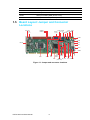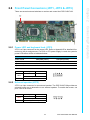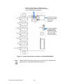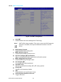
1
User Manual PCE-5128/7128 LGA1150 Intel® Core™7/i5/i3/Pentium®/ Xeon® PICMG 1.3 Single Host Board with VGA/ DVI-D/ (ECC)DDR3 /SATA3.0 / USB3.0 / Dual GbE Copyright The documentation and the software included with this product are copyrighted 2013 by Advantech Co., Ltd. All rights are reserved. Advantech Co., Ltd. reserves the right to make improvements in the products described in this manual at any time without notice. No part of this manual may be reproduced, copied, translated or transmitted in any form or by any means without the prior written permission of Advantech Co., Ltd. Information provided in this manual is intended to be accurate and reliable. However, Advantech Co., Ltd. assumes no responsibility for its use, nor for any infringements of the rights of third parties, which may result from its use. Acknowledgements AMIBIOS is a trademark of American Megatrends Inc. Intel®, Core™i7/i5/i3, Pentium® and Xeon are trademarks of Intel® Corporation. Nuvoton is a trademark of Nuvoton Technology Corp. All other product names or trademarks are the properties of their respective owners. Product Warranty (2 years) Advantech warrants to you, the original purchaser, that each of its products will be free from defects in materials and workmanship for two years from the date of purchase. This warranty does not apply to any products which have been repaired or altered by persons other than repair personnel authorized by Advantech, or which have been subject to misuse, abuse, accident or improper installation. Advantech assumes no liability under the terms of this warranty as a consequence of such events. Because of Advantech’s high quality-control standards and rigorous testing, most of our customers never need to use our repair service. If an Advantech product is defective, it will be repaired or replaced at no charge during the warranty period. For outof-warranty repairs, you will be billed according to the cost of replacement materials, service time and freight. Please consult your dealer for more details. If you think you have a defective product, follow these steps: 1. Collect all the information about the problem encountered. (For example, CPU speed, Advantech products used, other hardware and software used, etc.) Note anything abnormal and list any onscreen messages you get when the problem occurs. 2. Call your dealer and describe the problem. Please have your manual, product, and any helpful information readily available. 3. If your product is diagnosed as defective, obtain an RMA (return merchandise authorization) number from your dealer. This allows us to process your return more quickly. 4. Carefully pack the defective product, a fully-completed Repair and Replacement Order Card and a photocopy proof of purchase date (such as your sales receipt) in a shippable container. A product returned without proof of the purchase date is not eligible for warranty service. 5. Write the RMA number visibly on the outside of the package and ship it prepaid to your dealer. Part No. 2006512810 Edition 1 November 2013 PCE-5128/7128 User Manual ii Declaration of Conformity FCC Class A Note: This equipment has been tested and found to comply with the limits for a Class A digital device, pursuant to part 15 of the FCC Rules. These limits are designed to provide reasonable protection against harmful interference when the equipment is operated in a commercial environment. This equipment generates, uses, and can radiate radio frequency energy and, if not installed and used in accordance with the instruction manual, may cause harmful interference to radio communications. Operation of this equipment in a residential area is likely to cause harmful interference in which case the user will be required to correct the interference at his own expense. Caution! There is a danger of a new battery exploding if it is incorrectly installed. Do not attempt to recharge, force open, or heat the battery. Replace the battery only with the same or equivalent type recommended by the manufacturer. Discard used batteries according to the manufacturer's instructions. A Message to the Customer Advantech Customer Services Each and every Advantech product is built to the most exacting specifications to ensure reliable performance in the harsh and demanding conditions typical of industrial environments. Whether your new Advantech equipment is destined for the laboratory or the factory floor, you can be assured that your product will provide the reliability and ease of operation for which the name Advantech has come to be known. Your satisfaction is our primary concern. Here is a guide to Advantech’s customer services. To ensure you get the full benefit of our services, please follow the instructions below carefully. Technical Support We want you to get the maximum performance from your products. So if you run into technical difficulties, we are here to help. For the most frequently asked questions, you can easily find answers in your product documentation. These answers are normally a lot more detailed than the ones we can give over the phone. So please consult this manual first. If you still cannot find the answer, gather all the information or questions that apply to your problem, and with the product close at hand, call your dealer. Our dealers are well trained and ready to give you the support you need to get the most from your Advantech products. In fact, most problems reported are minor and are able to be easily solved over the phone. In addition, free technical support is available from Advantech engineers every business day. We are always ready to give advice on application requirements or specific information on the installation and operation of any of our products. iii PCE-5128/7128 User Manual Memory Compatibility PCE-5128 Compatible Memory Brand Transcend Size Speed Type ECC Vendor PN Memory 1GB DDR3 1066 N TS128MLK64V1U SEC K4B1G0846G-BCH9 96D3-1G1066NN-TR 2GB DDR3 1066 N TS256MLK64V1U SEC K4B1G0846G-BCH9 96D3-2G1066NN-TR 1GB DDR3 1333 N TS128MLK64V3U ELPIDA EDJ1108BFBGDJ-F 2GB DDR3 1333 N TS256MLK64V3U SEC K4B1G0846G-BCH9 96D3-2G1333NN-TR4 4GB DDR3 1333 N TS512MLK64V3N HYNIX H5TQ2G83CFR H9C 256x8 96D34G1333NN-TR 2GB DDR3 1600 N TS256MLK64V6N MICRON IRM72 D9PFJ NA 4GB DDR3 1600 N TS512MLK64V6N MICRON IUM22 D9PFJ NA NA NA 96D3-1G1333NN-TR 4GB DDR3 1600 N TS512MLK64V6N MICRON 2EM77 D9PFJ 256x8 8GB DDR3 1600 N TS1GLK64V6H micron IZD27 D9PBC 512x8 1GB DDR3 1066 N 78.01GC3.420 ELPIDA J1108BDBG-DJ-F 96D3-1G1066NN-AP (128x8) 2GB DDR3 1066 N 78.A1GC3.421 ELPIDA J1108BDBG-DJ-F 96D3-2G1066NN-AP (128x8) 4GB DDR3 1066 N 78.B1GDJ.AF1 HYNIX H5TQ2G83BFRH9C NA N 78.01GC6.AF0 H5TQ1G83DFR-H9C 96D3-1G1333NN-AP1 1GB DDR3 1333 DDR3 1333 2GB DDR3 1333 N 78.A1GDE.4200C ELPIDA J2108BCSE-DJ-F 96D3-2G1333NN-AP2 2GB DDR3 1333 N 78.A1GDE.AF00C Hynix H5TQ2G838FR(256x8) 96D3-2G1333NN-AP1 4GB DDR3 1333 N 78.B1GDE.AF1 HYNIX H5TQ2G83BFRH9C 96D3-4G1333NN-AP 4GB DDR3 1333 N 78.B1GDE.AF1 HYNIX H5TQ2G83BFR H9C 256x8 96D3-4G1333NN-AP 8GB DDR3 1333 N 78.C1GEP.4210C ELPIDA J4208BASE-DJ-F 78.C1GEP.4210C 512x8 8GB DDR3 1600 N 78.C1GET.ATF0C Micron 2FD27 D9PCP (512x8) NA 2GB DDR3 1333 N KVR1333D3S8N9/ 2G ELPIDA J2108BCSE-DJF(128x8) NA 4GB DDR3 1333 N KVR1333D3N9/4G KINGSTON D2568JENCPGD9U(512x NA 64) 2GB DDR3 1600 N XQ16A8N2GS-9-AV SEC K4B2G0846D (256x8) NA 2GB DDR3 1600 N XQ16A8N2GM-9-AV MICRON 2HM77 D9PFJ (256x8) NA 4GB DDR3 1600 N XQ16B8N4GS-9-AV SEC K4B2G0846D (256x8) NA 8GB DDR3 1600 N XQ16B8N8GS-9-AV SEC K4B4G0846B (512x8) NA 2GB DDR3 1600 N D3US56081XH12AA SEC 113 HCK0 K4B2G0846C 256x8 NA 4GB DDR3 1600 N D3US56082XH12AA SEC 113 HCK0 K4B2G0846C 256x8 NA H5TQ1G83TFR-H9C Apacer Kingston ATP DSL Advantech PN PCE-5128/7128 User Manual iv PCE-7128 compatible memory Brand Apacer ATP Transcend Size Speed Type ECC Vendor PN Memory Advantech PN NA 2GB 1066 DDR3 Y 78.A1GC5.423 ELPIDA J1108BDBGDJ-F (128x8) 4GB 1066 DDR3 Y 78.B1GDK.AF3 Hynix H5TQ2G83AFR H9C (256x8) NA 1GB 1333 DDR3 Y 78.01GC8.422 ELPIDA J1108BDBGDJ-F (128x8) 96D3-1G1333E-AP 2GB 1333 DDR3 Y 78.A1GC8.423 ELPIDA J1108BDBGDJ-F (128x8) 96D3-2G1333E-AP 4GB 1333 DDR3 Y 78.B1GDF.AF3 Hynix H5TQ2G83AFR H9C (256x8) NA 8GB 1600 DDR3 Y 78.C1GER.ATE0C MICRON 2AD27D9PBC NA 2GB 1333 DDR3 Y AQ56M72E8BJH9S SEC 952 HCH9 K4B1G0846E (128x8) NA 4GB 1333 DDR3 Y AQ12M72E8BKH9S SAMSUNG 928 K4B2G0846B-HCH9 (256x8) 96D3-4G1333E-AT 8GB 1333 DDR3 Y AQ24M72E8BLH9S SECK4B4G0846B 96D3-8G1333E-AT 8GB 1333 DDR3 Y TS1GLK72V3H 96D3-8G1333E-TR NA 8GB 1600 DDR3 Y TS1GLK64V6H micron IZD27 D9PBC 512x8 NA Specification Comparison Part Number PCH Memory VGA DVI-D Backplane LAN SATA3.0 USB3.0 USB2.0 RAID (4 for BP) AMT PCE-5128G200A1E Q87 Non-ECC Yes Yes*2 PCE-5BXX 2 GbE 6 3 9 Yes Yes PCE-7128G200A1E C226 ECC Yes Yes*2 PCE-5BXX/ 7BXX 2 GbE 6 3 9 Yes Yes Processor Support Architecture Model Processor Process Gen PCE-7128 Haswell PCE-5128/ 7128 22nm CPU Processor Advante ch P/N Base Freq. Socket LGA1150 (GHz) TBC E3-1275v3 TBC TBC L3 cache DDR3 memory speed support Cores/ Treads TDP 3.5GHz 8MB 4/8 95W Yes 9.0 E3-1225v3 3.2GHz 8MB 4/4 95W Yes 9.0 E3-1268v3 2.3GHz 8MB 4/8 45W Yes 9.0 96MPI73.18M10T Core I7-4770S 3.1GHz 8MB 4/8 65W No 9.0 96MPI72.38M10T Core I7-4770TE 2.3GHz 8MB 4/8 45W No 9.0 96MPI52.96M10T Core i5-4570S 2.9GHz 6MB 4/4 65W No 9.0 96MPI52.74M10T Core i5-4570TE 2.7GHz 4MB 2/4 35W Yes 9.0 TBC Core i3-4330 3.5GHz 4MB 2/4 54W Yes N/A TBC Core i3-4330TE 2.4GHz 3MB 2/4 35W Yes N/A TBC Pentium G3420 3.2GHz 3MB 2/2 54W Yes N/A TBC Pentium G3320TE 2.3GHz 3MB 2/2 35W Yes N/A ECC AMT 1600 v PCE-5128/7128 User Manual Backplane Support Matrix Table Backplane Model processor PCE-5XXX PCE-7XXX PCE-5128G2-00A1E Yes - PCE-7128G2-00A1E Yes Yes (Except PCE-7B10-04A1E) Note! If PCE-5128/7128 is used on different backplanes which has different PCIe configuration. Below message would be showed on first time power on, and user has to turn off AC power and then turn on for PCIe re-configuration. Caution! PCIe configuration error! Please turn off AC power before re-configuration. Initial Inspection Before you begin installing your motherboard, please make sure that the following materials have been shipped: 1 PCE-5128 or 7128 PICMG 1.3 Single Host Board 1 PCE-5128/7128 startup manual 1 CD with utility 1 User note for full-sized CPU card 2 Serial ATA HDD data cable 2 Serial ATA HDD power cable 1 COM + printer ports cable kit 1 4-port USB cable kit Keyboard and mouse Y cable 1 jumper package 1 warranty card P/N: 2002721020 P/N: 1700003194 P/N: 1703150102 P/N: 1701260305 P/N: 1700008461 P/N: 1700060202 P/N: 9689000068 If any of these items are missing or damaged, contact your distributor or sales representative immediately. We have carefully inspected the PCE-5128/7128 mechanically and electrically before shipment. It should be free of marks and scratches and in perfect working order upon receipt. As you unpack the PCE-5128/7128, check it for signs of shipping damage. (For example, damaged box, scratches, dents, etc.) If it is damaged or it fails to meet the specifications, notify our service department or your local sales representative immediately. Also notify the carrier. Retain the shipping carton and packing material for inspection by the carrier. After inspection, we will make arrangements to repair or replace the unit. PCE-5128/7128 User Manual vi Contents Chapter 1 Hardware Configuration......................1 1.1 1.2 1.3 1.9 1.10 1.11 1.12 1.13 Introduction ............................................................................................... 2 Features & Benefits................................................................................... 2 Specifications ............................................................................................ 3 1.3.1 System .......................................................................................... 3 1.3.2 Memory ......................................................................................... 3 1.3.3 Input/Output .................................................................................. 3 1.3.4 Graphics........................................................................................ 4 1.3.5 Ethernet LAN ................................................................................ 4 1.3.6 Industrial features ......................................................................... 4 1.3.7 Mechanical and environmental specifications............................... 4 Jumpers and Connectors .......................................................................... 5 Table 1.1: Jumper list .................................................................. 5 Table 1.2: Connectors ................................................................. 5 Board Layout: Jumper and Connector Locations...................................... 6 Figure 1.1 Jumper and connector locations................................. 6 Block Diagram........................................................................................... 7 Figure 1.2 PCE-5128 block diagram............................................ 7 Figure 1.3 PCE-7128 block diagram............................................ 7 Safety Precautions .................................................................................... 8 Jumper Settings ........................................................................................ 8 1.8.1 How to set jumpers ....................................................................... 8 1.8.2 BIOS CMOS (JCMOS1)................................................................ 9 Table 1.3: JCMOS1/JME1: clear CMOS/ME data....................... 9 1.8.3 Watchdog timer output (JWDT1) .................................................. 9 Table 1.4: Watchdog timer output (JWDT1) ................................ 9 Table 1.5: H/W monitor alarm (JOBS1)...................................... 9 Table 1.6: JERP1: Deep Sleep S5 .............................................. 9 System Memory ...................................................................................... 10 Memory Installation Procedures.............................................................. 10 Cache Memory........................................................................................ 10 Processor Installation.............................................................................. 10 Processor Cooler Installation .................................................................. 12 2 Connecting Peripherals ....................15 2.1 2.2 2.3 2.4 2.5 2.6 2.7 2.8 Introduction ............................................................................................. 16 Parallel Port (LPT1)................................................................................. 16 USB Ports (USB12, USB3, USB4, USB56, USB78) ............................... 16 VGA Connectors (VGA1) ........................................................................ 17 Serial Ports (COM1 & COM2) ................................................................. 17 PS/2 Keyboard and Mouse Connector (KBMS1/KBMS2)....................... 18 CPU Fan Connector (CPUFAN1)............................................................ 18 Front Panel Connectors (JFP1, JFP2 & JFP3) ....................................... 19 2.8.1 Power LED and keyboard lock (JFP3)........................................ 19 Table 2.1: PS/2 or ATX power supply LED status..................... 19 2.8.2 External speaker (JFP2) ............................................................. 19 2.8.3 Reset connector (JFP1) .............................................................. 20 2.8.4 HDD LED connector (JFP2)........................................................ 20 2.8.5 ATX soft power switch (JFP1)..................................................... 20 H/W Monitor/Watchdog Timer/Infrared ................................................... 21 2.9.1 H/W monitor alarm (JOBS1) ....................................................... 21 2.9.2 Watchdog timer (JWDT1) ........................................................... 21 2.9.3 Infrared interface (JIR1) .............................................................. 21 1.4 1.5 1.6 1.7 1.8 Chapter 2.9 vii PCE-5128/7128 User Manual 2.10 2.15 2.16 LAN Ports (LAN1 & LAN2)...................................................................... 22 Table 2.2: LAN LED Indicators.................................................. 22 High Definition Audio Module Interface (HDAUD1) ................................ 23 Figure 2.1 Jumper and connector locations of PCA-AUDIOHDA1E ..................................................................... 24 GPIO Header (GPIO1)............................................................................ 25 Case Open Connector (JCASE1) ........................................................... 25 Front Panel LAN Indicator Connector (LANLED1).................................. 26 Table 2.3: LAN LED Indicators.................................................. 26 Serial ATA Interface (SATA1~SATA6).................................................... 27 LPC Extension Interface (LPC1)............................................................. 27 3 AMI BIOS Setup................................. 29 3.1 Introduction ............................................................................................. 30 Figure 3.1 Setup program initial screen..................................... 30 Entering Setup ........................................................................................ 31 3.2.1 Main Setup.................................................................................. 31 Figure 3.2 Main setup screen .................................................... 31 3.2.2 Advanced BIOS Features Setup................................................. 32 Figure 3.3 Advanced BIOS features setup screen .................... 32 Figure 3.4 PCI Subsystem Settings........................................... 33 Figure 3.5 PCI Express Settings ............................................... 34 Figure 3.6 ACPI Settings ........................................................... 35 Figure 3.7 Trust Computing....................................................... 36 Figure 3.8 S5 RTC configuration ............................................... 37 Figure 3.9 CPU Configuration ................................................... 37 Figure 3.10SATA Configuration.................................................. 39 Figure 3.11Firmware Update Configuration ............................... 41 Figure 3.12AMT Configuration ................................................... 42 Figure 3.13USB Configuration.................................................... 43 Figure 3.14Smart Setting............................................................ 44 Figure 3.15Super IO Configuration............................................. 45 Figure 3.16Serial Port 1 Configuration ....................................... 45 Figure 3.17Serial Port 2 Configuration ....................................... 46 Figure 3.18Parallel Configuration ............................................... 46 Figure 3.19PC Health Status...................................................... 47 3.2.3 Chipset........................................................................................ 48 Figure 3.20Chipset ..................................................................... 48 Figure 3.21PCH IO Configuration............................................... 48 Figure 3.22PCI Express Configuration ....................................... 50 Figure 3.23USB Configuration.................................................... 51 Figure 3.24PCH Azalia Configuration......................................... 52 Figure 3.25System Agent (SA) Configuration ............................ 53 Figure 3.26Graphics Configuration............................................. 54 Figure 3.27NB PCIe Configuration ............................................. 55 Figure 3.28Memory Information ................................................. 56 3.2.4 Boot ............................................................................................ 56 Figure 3.29 Boot ......................................................................... 56 3.2.5 Security....................................................................................... 58 Figure 3.30Security .................................................................... 58 3.2.6 Save & Exit ................................................................................. 59 Figure 3.31Save & Exit............................................................... 59 2.11 2.12 2.13 2.14 Chapter 3.2 Chapter 4 Value-Added Software Services ...... 61 4.1 Value-Added Software Services ............................................................. 62 4.1.1 Software API............................................................................... 62 4.1.2 Software Utility............................................................................ 63 PCE-5128/7128 User Manual viii Chapter 5 Chipset Software Installation Utility 65 5.1 5.2 5.3 Before You Begin .................................................................................... 66 Introduction ............................................................................................. 66 Windows® 7 / Windows® 8 Driver Setup................................................ 67 6 Integrated Graphic Device Setup .....69 6.1 6.2 Introduction ............................................................................................. 70 Windows 7/ Windows 8 Driver Setup ...................................................... 70 7 LAN Configuration.............................71 7.1 7.2 7.3 Introduction ............................................................................................. 72 Installation ............................................................................................... 72 Win XP /Win 7 Driver Setup (LAN).......................................................... 72 8 Intel ME ...............................................73 8.1 8.2 Introduction ............................................................................................. 74 Installation ............................................................................................... 74 9 Intel USB 3.0.......................................75 9.1 9.2 Introduction ............................................................................................. 76 Installation ............................................................................................... 76 Chapter 10 SATA RAID Setup ..............................77 10.1 10.2 Introduction ............................................................................................. 78 SATA RAID Driver and Utility Setup ....................................................... 78 Appendix A Programming the Watchdog Timer..79 A.1 Introduction ............................................................................................. 80 A.1.1 Watchdog timer overview............................................................ 80 A.1.2 Programming the watchdog timer ............................................... 80 Table A.1: Watchdog timer registers.......................................... 81 A.1.3 Example program........................................................................ 82 Appendix B I/O Pin Assignments..........................87 B.1 Parallel Port Connector (LPT1) ............................................................... 88 Table B.1: Parallel port connector (LPT1).................................. 88 VGA Connector (VGA1) .......................................................................... 88 Table B.2: VGA connector (VGA1) ............................................ 88 RS 232 Serial Port (COM12)................................................................... 89 Table B.3: RS-232 serial port (COM2)....................................... 89 USB 2.0 Header (USB56 & 910)............................................................. 89 Table B.4: USB Header (USB56 & 910) .................................... 89 USB3.0 Header (USB12) ........................................................................ 90 Table B.5: USB 3.0 Header (USB12)......................................... 90 PS/2 Keyboard/Mouse Connector (KBMS1) ........................................... 90 Table B.6: PS/2 keyboard/mouse connector (KBMS1).............. 90 Chapter Chapter Chapter Chapter B.2 B.3 B.4 B.5 B.6 ix PCE-5128/7128 User Manual B.7 B.8 B.9 B.10 B.11 B.12 B.13 B.14 B.15 B.16 B.17 B.18 B.19 B.20 B.21 B.22 External Keyboard Connector (KBMS2) ................................................. 91 Table B.7: External keyboard connector (KBMS2) .................... 91 CPU Fan Power Connector (CPUFAN1) ................................................ 91 Table B.8: CPU fan power connector (CPUFAN1) .................... 91 Power LED and Keyboard Lock Connector (JFP3 / PWR_LED & KEY LOCK) ..................................................................................................... 91 Table B.9: Power LED and keyboard lock connector (JFP3 / PWR_LED & KEY LOCK) ........................................ 91 External Speaker Connector (JFP2 / SPEAKER) ................................... 92 Table B.10:External speaker connector (JFP2 / SPEAKER)...... 92 Reset Connector (JFP1 / RESET) .......................................................... 92 Table B.11:Reset connector (JFP1 / RESET) ............................ 92 HDD LED (JFP2 / HDDLED)................................................................... 92 Table B.12:HDD LED (JFP2 / HDDLED) .................................... 92 ATX Soft Power Switch (JFP1 / PWR_SW)............................................ 93 Table B.13:ATX soft power switch (JFP1 / PWR_SW)............... 93 Hi-definition Audio Link Connector (HDAUD1) ....................................... 93 Table B.14:Hi-definition audio link connector (HDAUD1) ........... 93 SM Bus Connector (JFP2 / SNMP)......................................................... 93 Table B.15:SM bus connector (JFP2 / SNMP) ........................... 93 LAN1 and LAN2 LED Connector (LANLED1) ......................................... 94 Table B.16:LAN1 and LAN2 LED connector (LANLED1) ........... 94 GPIO Header (GPIO1)............................................................................ 94 Table B.17:GPIO header (GPIO1).............................................. 94 Fixed I/O Ranges Decoded by Intel PCH ............................................... 95 Table B.18:Fixed I/O Ranges Decoded by PCH......................... 95 System I/O Ports..................................................................................... 96 Table B.19:System I/O Ports ...................................................... 96 Interrupt Assignments ............................................................................. 97 Table B.20:Interrupt Assignments .............................................. 97 1 MB Memory Map.................................................................................. 97 Table B.21:1 MB memory map ................................................... 97 PCI Bus Map........................................................................................... 97 Table B.22:PCI Bus Map ............................................................ 97 Appendix C Programming the GPIO .................... 99 C.1 C.2 C.3 Supported GPIO Register ..................................................................... 100 GPIO Registers..................................................................................... 100 GPIO Example Program-1 .................................................................... 100 PCE-5128/7128 User Manual x Chapter 1 Hardware Configuration 1 1.1 Introduction PCE-5128/7128 is a PICMG 1.3 form-factor single host board which is designed with Intel®Q87 (PCE-5128) and C226 (PCE-7128) PCH for industrial applications that need high computing power and strong I/O capability. PCE-5128/7128 supports 22nm manufacturing technology, LGA1150 socket Intel® Core™ i7/i5/i3, Pentium® and Xeon™ processors that integrate memory and graphic controllers and support DDR3 1333/1600 MHz SDRAM up to 16 GB. With advanced computing technology, PCE-5128/7128 is suitable for processor hungry industrial applications. PCE-5128/7128 performs excellent graphics capability with its integrated Intel® HD Graphics core with a minimum 1GB shared memory (requires a minimum 2GB system memory). With this, PCE-5128/7128 provides strong 2D/3D graphics processing power without an additional graphic card to save extra cost, power consumption and thermal integration effort. PCE-5128/7128 also has rich I/O interface, which can support Advantech PCE-5BXX and 7BXX backplanes to offer various expansion slots such as PCI, PCI-X and PCIe slots with its PCIe lanes that are configured as one x16, or two x8 and four x1. New SATA Gen3 (600MB/sec) ports satisfy high data applications, like storage and DVR. Six SATA ports support software RAID 0, 1, 5, 10 for a cost-effective reliable data solution. Three USB 3.0 ports reach 5Gbps high data rates, and two on-board RS-232 serial COM ports are for industrial control applications. With flexible I/O and graphic expansibility, PCE-5128/7128 can be an excellent, cost effective graphic or I/ O oriented workstation class hardware platform. With outstanding performance and exceptional features, PCE-5128/7128 is the ideal computing platform for advanced industrial applications. 1.2 Features & Benefits Features Benefits Intel’s 4th generation Core i7/i5/i3/Pentium/Xeon PCE-5128/7128 supports Intel 4th gener- processor cores with quad/dual-core computing ation processors power brings quantum-leap performance improvement. PCE-5128/7128 supports DDR3 1333/ 1600 SDRAM up to 16 GB Provides higher memory data transmission and processing efficiency, bringing higher system performance. *PCE-7128 supports ECC memory, but PCE-5128 does not. PCE-5128 supports one x16 lane(s) for supporting PCE-5BXX series BPs. PCE-5128 supports one x16 lane(s) for Advantech backplanes 5BXX series. PCE-7128 supports dual PCIe x8 or one PCE-7128 supports dual PCIe x8 or one x16 x16 lane(s) for supporting both PCElane(s) for Advantech backplanes: PCE-7BXX and 7BXX/5BXX series BPs. 5BXX series with single or dual PCIe x8 slot(s). Reduces customer S/W development effort with Fully supports Advantech SUSI APIs and more reliable S/W quality, also provides valueUtilities. added utilities such as system monitor and Embedded Security ID. SATA Gen3 Provides high performance storage interface. SATA Gen3 is 6Gb/s which is double bandwidth with SATA Gen2. USB 3.0 Provides high transfer data performance interface; USB 3.0 data transfer rate is 5Gbps which is 10 times faster than USB2.0. PCE-5128/7128 User Manual 2 1.3 Specifications 1.3.1 System Note! PCE-5128/7128 does NOT support PATA(IDE) interface. Only PCE-7128 supports Intel Xeon processors. 1.3.2 Memory RAM: – PCE-5128: Up to 16 GB in two 240-pin DIMM sockets. Supports dual-channel DDR3 1333/1600 MHz SDRAM WITHOUT ECC function. – PCE-7128: Up to 16 GB in two 240-pin DIMM sockets. Supports dual-channel DDR3 1333/1600 MHz SDRAM WITH or WITHOUT ECC function. Note! 1. 2. Due to the inherent limitations of the PC architecture, the system may not fully detect 16 GB RAM when 16 GB of RAM is installed. A 32-bit OS may not fully detect 4 GB of RAM when 4 GB is installed. 1.3.3 Input/Output PCIe bus: One PCIex16 or Two PCIex8 from CPU and One PCIe x4 from PCH PCI bus: Four PCI masters to the backplane, 32-bit, 33 MHz PCI 2.2 compliant. Enhanced parallel port: This EPP/SPP/ECP port can be configured to LPT1, LPT2, LPT3 or disabled. A standard DB-25 female connector provided. Serial ports: Two RS-232 serial ports PS/2 keyboard and mouse connector: One 6-pin mini-DIN connectors is located on the mounting bracket for easy connection to a PS/2 keyboard and mouse via the Y-cable included in the package. USB port: Supports 9 x USB 2.0 ports with transfer rates up to 480 Mbps. (5 ports are on the CPU card and 4 ports are on the backplane), and 3 USB 3.0 ports with transfer rates of up to 5 Gbps. LPC: One LPC connector to support Advantech TPM LPC modules. GPIO: Supports 8-bit GPIO from super I/O for general purpose control application. 3 PCE-5128/7128 User Manual Hardware Configuration CPU: LGA1150-socket Core i7/i5/i3, Pentium and Xeon E3-1200v3 series processors L2 Cache: Please refer to CPU specification for detailed information. BIOS: AMI SPI BIOS (128 Mb SPI) System Chipset: Intel Q87(PCE-5128); Intel C226(PCE-7128) SATA hard disk drive interface: Six SATA3 (600MB/s) are with blue connectors. These interfaces can be enabled/disabled in the BIOS. Chapter 1 PCE-5128/7128 provides three independent displays, VGA+DVI-D+DVI-D. note: requires 2 x DVID cables for DVI-D output. Triple display 1.3.4 Graphics Controller: Intel® HD Graphics embedded in the processor. Display memory: Shared memory is subject to OS (install 2 GB or above memory for basic system configuration). CRT: Up to 2048 x 1536 resolution, 400 MHz RAMDAC. DVI-D: Two DVI-D pin header ports support resolution up to 1920 x 1200 @ 60 Hz. PCI express x16/x8 slot on the backplane: An external graphic card can be installed in the PCIe x16 / x8 slot for high 2D/3D graphics capability. 1.3.5 Ethernet LAN Supports single/dual 10/100/1000 Mbps Ethernet port(s) via the dedicated PCI Express x1 bus which provides 500 MB/s data transmission rate. Controller: – LAN 1: Intel® I217LM for both PCE-5128 and PCE-7128. – LAN 2: Intel® I211(PCE-5128) and I210(PCE-7128). 1.3.6 Industrial features Watchdog timer: Can generate a system reset. The watchdog timer is programmable, with each unit equal to one second or one minute (255 levels). 1.3.7 Mechanical and environmental specifications Operating temperature: 0 ~ 60° C (32 ~ 140° F, Depending on CPU and thermal solution) Storage temperature: -40 ~ 85° C (-40 ~ 185° F) Humidity: 20 ~ 95% non-condensing Power supply voltage: +3.3 V, +5 V, +12 V, +5 VSB Power consumption: Processor: Intel Core i7-4770S; Memory: DDR3 1600 8GB x 2 Voltage +12 V +5 V +3.3 V +5 VSB Current 4.02 A 1.36 A 0.81 A 0.09 A Board size: 338.58 mm (L) x 126.39 mm (W) (13.3" x 4.98") Board weight: 0.5 kg PCE-5128/7128 User Manual 4 Connectors on the PCE-5128/7128 single host board link it to external devices such as hard disk drives and a keyboard. In addition, the board has a number of jumpers used to configure your system for your application. The tables below list the function of each of the board jumpers and connectors. Later sections in this chapter give instructions on setting jumpers. Chapter 2 gives instructions for connecting external devices to your motherboard. Label Function JCMOS1 CMOS clear JME1 Clear ME data JWDT1 Watchdog timer output selection JOBS1 HW Monitor Alarm Table 1.2: Connectors Label Function LPT1 Parallel port, Parallel port x 1, supports SPP/EPP/ECP mode LAN1 Intel I217LM for all SKUs LAN2 Intel I211(PCE-5128); Intel I210AT(PCE-7128) VGA1 VGA connector KBMS1 PS/2 keyboard and mouse connector KBMS2 External keyboard/mouse connector COM1 Serial port: COM1; RS-232 (9-pin Box Header) COM2 Serial port: COM2; RS-232 (9-pin Box Header) JIR1 Infrared connector JFP3 (Keyboard Lock and Power LED) Power LED Suspend: Fast flash (ATX/AT) System On: ON (ATX/AT) System Off: OFF ((ATX/AT)) JFP2 External speaker / SATA HDD LED connector JFP1 Power Switch / Reset connector JCASE1 Case Open CPUFAN1 CPU FAN connector (4-pin) LANLED1 LAN1/2 LED extension connector HDAUD1 HD audio extension module connector USB12 USB port 1, 2 USB3 USB port 3 USB4 USB port 4 USB56 USB port 5, 6 USB78 USB port 7, 8 SATA1 Serial ATA1 SATA2 Serial ATA2 SATA3 Serial ATA3 SATA4 Serial ATA4 SATA5 Serial ATA5 SATA6 Serial ATA6 5 PCE-5128/7128 User Manual Hardware Configuration Table 1.1: Jumper list Chapter 1 1.4 Jumpers and Connectors CPU1 CPU Socket DIMMA1 Memory connector channel A DIMMB1 Memory connector channel B GPIO1 GPIO pin header (SMD pitch-2.0 mm) LPC1 COM port module expansion pin-header 1.5 Board Layout: Jumper and Connector Locations CPU FAN1 JFP 1¥3 DIMM B1 DIMM A1 SATA3 1,2,4,5 USB12 SATA3 3,6 LPT1 COM1 USB4 COM2 USB78 LANLED1 USB56 USB3 JCASE1 LAN2 LAN1 VGA1 KBMS1 CPU1 JERP1 DVI1 DVI2 JIR1 JOBS1 JWDT1 PCH 1 JCMOS1 JME1 HD GPIO1 AUDIO1 SPI_CN1 BMC1 (PCE-7128) LPC1 Figure 1.1 Jumper and connector locations PCE-5128/7128 User Manual 6 KBMS2 Chapter 1 1.6 Block Diagram Figure 1.3 PCE-7128 block diagram 7 PCE-5128/7128 User Manual Hardware Configuration Figure 1.2 PCE-5128 block diagram 1.7 Safety Precautions Warning! Always completely disconnect the power cord from your chassis whenever you work with the hardware. Do not make connections while the power is on. Sensitive electronic components can be damaged by sudden power surges. Only experienced electronics personnel should open the PC chassis. Caution! Always ground yourself to remove any static charge before touching the motherboard. Modern electronic devices are very sensitive to static electrical discharges. As a safety precaution, use a grounding wrist strap at all times. Place all electronic components on a static-dissipative surface or in a static-shielded bag when they are not in the chassis. Caution! The computer is provided with a battery-powered Real-time Clock. There is a danger of explosion if battery is incorrectly replaced. Replace only with same or equivalent type recommended by the manufacturer. Discard used batteries according to manufacturer's instructions. Caution! There is a danger of a new battery exploding if it is incorrectly installed. Do not attempt to recharge, force open or heat the battery. Replace the battery only with the same or equivalent type recommended by the manufacturer. Discard used batteries according to the manufacturer’s instructions. 1.8 Jumper Settings This section provides instructions on how to configure your motherboard by setting the jumpers. It also includes the motherboard’s default settings and your options for each jumper. 1.8.1 How to set jumpers You can configure your motherboard to match the needs of your application by setting the jumpers. A jumper is a metal bridge that closes an electrical circuit. It consists of two metal pins and a small metal clip (often protected by a plastic cover) that slides over the pins to connect them. To “close” (or turn ON) a jumper, you connect the pins with the clip. To “open” (or turn OFF) a jumper, you remove the clip. Sometimes a jumper consists of a set of three pins, labeled 1, 2 and 3. In this case you connect either pins 1 and 2, or 2 and 3. A pair of needle-nose pliers may be useful when setting jumpers. PCE-5128/7128 User Manual 8 The PCE-5128/7128 CPU card contains a jumper that can erase BIOS CMOS/ME data and reset the system BIOS information. Normally this jumper should be set with pins 1-2 closed. If you want to reset those data, set JCMOS1/JME1 to 2-3 closed for just a few seconds, and then move the jumper back to 1-2 closed. This procedure will reset the CMOS/ME to its last status or default setting. Chapter 1 1.8.2 BIOS CMOS (JCMOS1) Table 1.3: JCMOS1/JME1: clear CMOS/ME data Jumper Setting 1 *Keep BIOS CMOS/ME data 1-2 closed Clear BIOS CMOS/ME data 2-3 closed * default setting 1.8.3 Watchdog timer output (JWDT1) The PCE-5128/7128 contains a watchdog timer that will reset the CPU in the event the CPU stops processing. This feature means the PCE-5128/7128 will recover from a software failure or an EMI problem. The JWDT1 jumper settings control the outcome of what the computer will do in the event the watchdog timer is tripped. Table 1.4: Watchdog timer output (JWDT1) Function Jumper Setting 1 * Reset 2-3 closed 1 * Reserved 1-2 closed *default setting Table 1.5: H/W monitor alarm (JOBS1) Function Jumper Setting 1 Enabled 2 1-2 closed 1 Disabled 2 1-2 opened (JOBS1) is a 2-pin connector for setting enable/disable alarm while the on-board security event acts. Table 1.6: JERP1: Deep Sleep S5 Close Pins Result 1-2 Enable 2-3 Disable (Default) 9 PCE-5128/7128 User Manual Hardware Configuration Function 1.9 System Memory PCE-5128/7128 has two 240-pin memory sockets for (ECC) DDR3 1600 MHz memory modules with maximum capacity of 16 GB. (Maximum 8 GB for each DIMM) PCE-5128 supports non-ECC DDR3 memory modules. PCE-7128 supports ECC and non-ECC DDR3 memory modules. Note! Both of PCE-5128 and PCE-7128 do NOT support registered DIMMs (RDIMMs). 1.10 Memory Installation Procedures To install DIMMs, first make sure the two handles of the DIMM socket are in the “open” position. i.e. the handles lean outward. Slowly slide the DIMM module along the plastic guides on both ends of the socket. Then press the DIMM module right down into the socket, until you hear a click. This is when the two handles have automatically locked the memory module into the correct position of the DIMM socket. To remove the memory module, just push both handles outward, and the memory module will be ejected by the mechanism in the socket. Note! Because PCE-5128/7128 supports Intel Active Management Technology 9.0(AMT9.0) which utilizes some memory space of channel 0, it's suggested that the user should not leave channel 0 DIMM slots (DIMMA1) empty, or it may cause some system abnormality. 1.11 Cache Memory CPUs supported by PCE-5128/7128 have 8 MB, 6 MB, 3 MB L3 cache memory sizes. Note! Please refer to Intel CPU data sheet for detail information. 1.12 Processor Installation Warning! Without a fan or heat sink, the processor will overheat and cause damage to both the processor and the single board computer. To install a processor, first turn off your system. The PCE-5128/7128 is designed for Intel® LGA 1150 socket processors. PCE-5128/7128 User Manual 10 2. Remove the socket protection cap. 3. Align the cuts on the processor with the edges of the socket. 11 Hardware Configuration Pull the bar beside the processor socket outward and lift it. Chapter 1 1. PCE-5128/7128 User Manual 4. Replace the socket cap; lower the retainer bar and clip it shut. 5. Finished processor installation. 1.13 Processor Cooler Installation Purchasing PCE-5128/7128 optimized CPU cooler (P/N: 1960047831N001) from Advantech is a must. Other brand CPU coolers are NOT compatible with PCE-5128/ 7128. Advantech offers a specially designed CPU cooler for PCE-5128/7128 for better heat dissipation efficiency and enhancing rigidity of CPU card, part number 1960047831N001. PCE-5128/7128 CPU is NOT compatible with other brand CPU coolers (neither is it compatible with Intel boxed CPU cooler). Please install 1960047831N001 CPU cooler following these instructions: PCE-5128/7128 User Manual 12 13 PCE-5128/7128 User Manual Hardware Configuration Note the direction of CPU cooler; it must follow that shown above. Installing a CPU cooler in the wrong direction may cause poor heat dissipation that may damage the CPU card. Chapter 1 Attach the CPU cooler on CPU card by fastening four screws of the CPU cooler into the steel back-plate on PCB. PCE-5128/7128 User Manual 14 Chapter 2 Connecting Peripherals 2 2.1 Introduction You can access most of the connectors from the top of the board. If you have a number of cards installed, you may need to partially remove the card to make all the connections. 2.2 Parallel Port (LPT1) LPT1 The parallel port is normally used to connect the motherboard to a printer. The PCE5128/7128 includes an onboard parallel port, accessed through a 26-pin flat-cable connector, LPT1. 2.3 USB Ports (USB12, USB3, USB4, USB56, USB78) The PCE-5128/7128 provides up to 8 USB (Universal Serial Bus) on-board ports with complete Plug & Play and hot swap support for up to 127 external devices. These USB ports comply with USB Specification 2.0 and 3.0, and support transfer rates up to 480 Mbps (USB2.0) and 5 Gbps (USB 3.0). The USB interface can be disabled in the system BIOS setup. USB12 USB4 USB78 USB56 USB3 PCE-5128/7128 User Manual 16 Chapter 2 2.4 VGA Connectors (VGA1) This CPU card has VGA outputs that can drive conventional CRT displays. VGA1 is a standard 15-pin D-SUB connector commonly used for VGA. 2.5 Serial Ports (COM1 & COM2) COM1 COM2 The PCE-5128/7128 offers two serial ports. These ports can connect to serial devices, such as a mouse or a printer, or to a communications network. The IRQ and address ranges for both ports are fixed. However, if you want to disable the port or change these parameters later, you can do this in the system BIOS setup. Optional dual COM cable, 1701092300, is available as well. 17 PCE-5128/7128 User Manual Connecting Peripherals VGA1 2.6 PS/2 Keyboard and Mouse Connector (KBMS1/ KBMS2) KBMS1 KBMS2 Two on-board 6-pin mini-DIN connectors (KBMS1) provide connection to a PS/2 keyboard and mouse by the Y-cable (1700060202) in the package. The on-board KBMS2 pin header provides connection to the front panel PS/2 keyboard and mouse connector of the chassis. 2.7 CPU Fan Connector (CPUFAN1) This fan connector supports 3-pin or 4-pin fan coolers and smart fan functions. Note: Fan speed is controlled by voltage. CPU FAN1 PCE-5128/7128 User Manual 18 There are several external switches to monitor and control the PCE-5128/7128. JFP 1¥3 JFP3 is a 5-pin connector for the power LED. Refer to Appendix B for detailed information on the pin assignments. If a PS/2 or ATX power supply is used, the system’s power LED status will be as indicated below: Table 2.1: PS/2 or ATX power supply LED status Power mode LED (PS/2 power) LED (ATX power) System On On On System Suspend Flashes Flashes System Off Off Off JFP1 JFP2 JFP3 PWR_SW Reset HDD LED SNMP Speaker PWR_LED & Key Lock 2.8.2 External speaker (JFP2) JFP2 is a 4-pin connector for an external speaker. The PCE-5128/7128 provides an onboard buzzer as an alternative to an external speaker. To enable the buzzer, set pins 3 and 4 as closed. JFP1 JFP2 JFP3 PWR_SW Reset HDD LED SNMP Speaker PWR_LED & Key Lock 19 PCE-5128/7128 User Manual Connecting Peripherals 2.8.1 Power LED and keyboard lock (JFP3) Chapter 2 2.8 Front Panel Connectors (JFP1, JFP2 & JFP3) 2.8.3 Reset connector (JFP1) Many computer cases offer the convenience of a reset button. Connect the wire from the reset button. JFP1 JFP2 JFP3 PWR_SW Reset HDD LED SNMP Speaker PWR_LED & Key Lock 2.8.4 HDD LED connector (JFP2) You can connect an LED to connector JFP2 to indicate when the HDD is active. JFP1 JFP2 JFP3 PWR_SW Reset HDD LED SNMP Speaker PWR_LED & Key Lock 2.8.5 ATX soft power switch (JFP1) If your computer case is equipped with an ATX power supply, you should connect the power on/off button on your computer case to JFP1. This connection enables you to turn your computer on and off. JFP1 JFP2 JFP3 PWR_SW Reset HDD LED SNMP Speaker PWR_LED & Key Lock PCE-5128/7128 User Manual 20 JWDT1 JOBS1 J JIR1 2.9.1 H/W monitor alarm (JOBS1) This 2-pin header is for enabling/disabling H/W monitor alarm function. Closed: Enables OBS Alarm Open: Disables OBS Alarm 2.9.2 Watchdog timer (JWDT1) This is for setting action trigger by watchdog timer. 1-2 Pin Close: No Action 2-3 Pin Close: System Reset 2.9.3 Infrared interface (JIR1) This is a 5-pin header for an infrared device. 21 PCE-5128/7128 User Manual Connecting Peripherals JIR1 JOBS1 JWDT1 Chapter 2 2.9 H/W Monitor/Watchdog Timer/Infrared 2.10 LAN Ports (LAN1 & LAN2) LAN2 LAN1 The PCE-5128/7128 is equipped with one or two high-performance 1000 Mbps Ethernet LANs. They are supported by all major network operating systems. The RJ45 jacks on the rear plate provide convenient connectivity. Table 2.2: LAN LED Indicators LAN Mode 1000Mbps Link On LED1 LED2 Green On On 1000Mbps Active Green on Flash 1000Mbps Link Off Off Off 100Mbps Link On Orange On On 100Mbps Active Orange On Flash 100Mbps Link Off Off Off 10Mbps Link On Off On 10Mbps Active Off Flash 10Mbps Link Off Off Off PCE-5128/7128 User Manual 22 Chapter 2 2.11 High Definition Audio Module Interface (HDAUD1) This HDAUD1 pin header is the connection interface to Advantech's 7.1 channel high definition audio module. Note! Advantech 7.1 channel high definition audio module ordering information. P/N: PCA-AUDIO-HDA1E 23 PCE-5128/7128 User Manual Connecting Peripherals HD AUDIO1 Connect CDIN1 with the CD/DVD drive's CD-in connector with the audio line included in the CD/DVD drive accessory i Connect CN1 with the power supply's 4-pin power connector Connect HDAUD1 to the HDAUD1 pinheader on the CPU card with the HD audio cable (PN:1701120251) Figure 2.1 Jumper and connector locations of PCA-AUDIO-HDA1E Note! Please remove the yellow jumper cap on the CPU card's HDAUD1 pinheader before connecting the HD audio cable to it. PCE-5128/7128 User Manual 24 Chapter 2 2.12 GPIO Header (GPIO1) Provides 10-pin header connector for 8-bit Digital I/O usage. Refer to Appendix B for detailed information on the pin assignments and programming guide in Appendix C. 2.13 Case Open Connector (JCASE1) JCASE1 The 2-pin case open connector is for chassis with a case open sensor. When the case is open, the buzzer on motherboard will beep. 25 PCE-5128/7128 User Manual Connecting Peripherals GPIO1 2.14 Front Panel LAN Indicator Connector (LANLED1) Table 2.3: LAN LED Indicators LAN Mode LED1 LED2 1000Mbps Link On Green On On 1000Mbps Active Green on Flash 1000Mbps Link Off Off Off 100Mbps Link On Orange On On 100Mbps Active Orange On Flash 100Mbps Link Off Off Off 10Mbps Link On Off On 10Mbps Active Off Flash 10Mbps Link Off Off Off LANLED1 PCE-5128/7128 User Manual 26 SATA3 1,2,4,5 Chapter 2 2.15 Serial ATA Interface (SATA1~SATA6) SATA3 3,6 Note! We recommend to plug CD/DVD drives on SATA3~6. When you install Linux OS, we recommend you to set AHCI mode in BIOS setting. It may recognize no hard drives when you use IDE mode during Linux OS installation. 2.16 LPC Extension Interface (LPC1) LPC1 LPC1 is a 14-pin female pin header for connection with an Advantech LPC module. 27 PCE-5128/7128 User Manual Connecting Peripherals The PCE-5128/7128 features high performance serial ATA interface (2* 600MB/s and 4* 300MB/s) which eases cabling to hard drivers or CD/DVD drivers with long cables. These six on-board SATA ports can be configured as RAID 0, 1, 10, or 5. Please see the detailed BIOS setting instructions for this in Chapter 3. PCE-5128/7128 User Manual 28 Chapter 3 AMI BIOS Setup 3 3.1 Introduction AMI BIOS has been integrated into motherboards for over a decade. In the past, people often referred to the AMI BIOS setup menu as BIOS, BIOS setup or CMOS setup. With the AMI BIOS Setup program, you can modify BIOS settings and control the special features of your computer. The Setup program uses a number of menus for making changes and turning the special features on or off. This chapter describes the basic navigation of the PCE-5128/7128 setup screens. Figure 3.1 Setup program initial screen PCE-5128/7128 User Manual 30 Turn on the computer and the BIOS is activated as well. The setup program can be triggered by pressing "DEL" or "F2" key. Note! If the message disappears before you press the "DEL" or "F2" key, please restart the computer and try it again. When you first enter the BIOS Setup Utility, you will enter the Main setup screen. You can always return to the Main setup screen by selecting the Main tab. There are two Main Setup options. They are described in this section. The Main BIOS Setup screen is shown below. Figure 3.2 Main setup screen The Main BIOS setup screen has two main frames. The left frame displays all the options that can be configured. Grayed-out options cannot be configured; options in blue can. The right frame displays the key legend. Above the key legend is an area reserved for a text message. When an option is selected in the left frame, it is highlighted in white. Often a text message will accompany it. System Time / System Date Use this option to change the system time and date. Highlight System Time or System Date using the <Arrow> keys. Enter new values through the keyboard. Press the <Tab> key or the <Arrow> keys to move between fields. The date must be entered in MM/DD/YY format. The time must be entered in HH:MM:SS format. 31 PCE-5128/7128 User Manual AMI BIOS Setup 3.2.1 Main Setup Chapter 3 3.2 Entering Setup 3.2.2 Advanced BIOS Features Setup Select the Advanced tab from the PCE-5128/7128 setup screen to enter the Advanced BIOS Setup screen. You can select any of the items in the left frame of the screen, such as CPU Configuration, to go to the sub menu for that item. You can display an Advanced BIOS Setup option by highlighting it using the <Arrow> keys. All Advanced BIOS Setup options are described in this section. The Advanced BIOS Setup screen is shown below, and the sub menus are described on the following pages. Figure 3.3 Advanced BIOS features setup screen PCE-5128/7128 User Manual 32 Chapter 3 3.2.2.1 PCI Subsystem Settings AMI BIOS Setup Figure 3.4 PCI Subsystem Settings PCI Common Settings PCI Latency Timer Value to be programed into PCI Latency Timer Register. VGA Palette Snoop Enables/Disables VGA palette registers snooping. 33 PCE-5128/7128 User Manual Figure 3.5 PCI Express Settings Maximum Payload Set maximum payload of PCI express device or allow system BIOS to select the value. Link Training Retry Defines number of retry attempts software will take to retrain the link if previous training attempt was unsuccessful. Link Training Timeout Defines number of micro-seconds software will wait before polling "Link Training " bit in link status register. Value range from 10 to 1000 uS. PCE-5128/7128 User Manual 34 Chapter 3 3.2.2.2 ACPI Settings AMI BIOS Setup Figure 3.6 ACPI Settings Power Type Choose this item correspond with your power supply type ATX or AT. Enable Hibernation "Enable or disable" Hibernate (OS/S4 Sleep State). This option may not be effective with some OS. PowerOn by Modem "Enabled" or "Disabled" PowerOn by Modem 35 PCE-5128/7128 User Manual 3.2.2.3 Trust Computing Figure 3.7 Trust Computing Security Device Support Enable or disable BIOS for security device support. You can purchase Advantech TPM (Trust Platform Module) PCA-TPM-00A1E for your security device. PCE-5128/7128 User Manual 36 Chapter 3 3.2.2.4 S5 RTC Wake Setting AMI BIOS Setup Figure 3.8 S5 RTC configuration Wake System with Fixed Time Enable or disable system wake on alarm event, When enabled, the system will wake on the hr:min:sec as specified. 3.2.2.5 CPU Configuration Figure 3.9 CPU Configuration 37 PCE-5128/7128 User Manual Active Processor Core Use this to select how many processor cores you want to activate when you are using a dual or quad core processor. Overclocking lock Enable or Disable the overclocking lock function. Limit CPUID Maximum Setting this item to [Enable] allows legacy operating systems to boot even without support for CPUs with extended CPUID functions. Execute Disable Bit This item specifies the Execute Disable Bit Feature. The settings are Enabled and Disabled. The Optimal and Fail-Safe default setting is Enabled. If Disabled is selected, the BIOS forces the XD feature flag to always return to 0. Intel Virtualization Technology This feature is used to enable or disable the Intel Virtualization Technology (IVT) extension. It allows multiple operating systems to run simultaneously on the same system. It does this by creating virtual machines, each running its own x86 operating system. Hardware Prefetcher Hardware Prefetcher is a technique that fetches instructions and/or data from memory into the CPU cache memory well before the CPU needs it, so that it can improve the load-to-use latency. You may choose to enable or disable it. Adjacent Cache Line Prefetch The Adjacent Cache-Line Prefetch mechanism, like automatic hardware prefetch, operates without programmer intervention. When enabled through the BIOS, two 64-byte cache lines are fetched into a 128-byte sector, regardless of whether the additional cache line has been requested or not. You may choose to enable or disable it. CPU C states Intel C states setting for power saving. Intel TXT(LT) Support Enable or Disable Intel TXT support PCE-5128/7128 User Manual 38 Chapter 3 3.2.2.6 SATA Configuration AMI BIOS Setup Figure 3.10 SATA Configuration SATA Controller(s) Enable or disable SATA Device SATA Mode This can be configured as IDE, RAID, and AHCI 39 PCE-5128/7128 User Manual SATA Controller Speed Sets the maximum speed of SATA controllers, and there are three modes, Gen1, Gen2, and Gen3. OROM UI Delay When this item is enabled, users are able to indicate the delay of the OROM UI Splash Screen under normal status. Port 1~6 To enable or disable SATA port 0~5. Hot Plug Enable/Disable SATA Hot-Plug Port 1~6 Device Type To identify the SATA that is connected to a Solid State or Hard Disk Drive. Note! Some OS request to install under AHCI mode so please consult your local OS vendor for more detailed information. i.e. Fedora and Ubuntu requests to install under AHCI mode. . PCE-5128/7128 User Manual 40 Chapter 3 3.2.2.7 PCH-FW Configuration AMI BIOS Setup Figure 3.11 Firmware Update Configuration ME FW Image Re-Flash Enable/Disable ME FW Image Re-Flash function. 41 PCE-5128/7128 User Manual 3.2.2.8 AMT Configuration Figure 3.12 AMT Configuration Intel AMT Enable/Disable Intel Active Management Technology. Note! iAMT H/W is always enabled. This option controls the BIOS extension execution. If enabled, this requests additional firmware in the SPI device. BIOS Hotkey Pressed Enable/Disable BIOS hotkey press. MEBx Selection Screen Enable/Disable MEBx selection screen. Hide Un-Configure ME Confirmation Hide un-configured ME without password confirmation prompt. MEBx Debug Message Output Enable MEBx debug message output. Un-Configure ME Un-configure ME without password. Amt Wait Timer Set timer to wait before sending ASF_GET_Boot_Options. Disable ME Set ME to soft temporary disable. ASF Enable/Disable alert specification format. Active Remote Assistance Process Trigger CIRA boot. PCE-5128/7128 User Manual 42 USB Configure Enable/Disable USB configure function. PET Progress User can Enable/Disable PET events progress to receive PET events or note. WatchDog Enable/Disable Watchdog Timer Chapter 3 3.2.2.9 USB Configuration AMI BIOS Setup Figure 3.13 USB Configuration Legacy USB Support This is for USB device support under legacy OS such as DOS. When choosing "AUTO", the system will automatically detect if any USB device is plugged into the computer and enable USB legacy mode when a USB device is plugged in, and disable USB legacy mode when no USB device is plugged in. USB3.0 support Enable/Disable USB3.0 (XHCI) support XHCI Hand-off This is a workaround for OS without XHCI hand-off support. The XHCI ownership change should be claimed by XHCI driver. EHCI Hand-off This is a workaround for OS without EHCI hand-off support. The EHCI ownership change should be claimed by EHCI driver. USB Mass Storage Driver Support Enable/Disable USB Mass Storage Driver Support USB transfer time-out Allows you to select the USB transfer time-out value. [1,5,10,20sec] Device reset time-out Allows you to select the USB device reset time-out value. [1,5,10,20sec] 43 PCE-5128/7128 User Manual Device power-up delay This item appears only when you set device power-up delay item to [manual]. USB Flash Driver PMAP 3.2.2.10 Smart Setting Figure 3.14 Smart Setting Smart self test Run SMART self test on all HDDs during POST. PCE-5128/7128 User Manual 44 Chapter 3 3.2.2.11 Super IO Configuration AMI BIOS Setup Figure 3.15 Super IO Configuration Figure 3.16 Serial Port 1 Configuration 45 PCE-5128/7128 User Manual Figure 3.17 Serial Port 2 Configuration Figure 3.18 Parallel Configuration Serial Port 1 -2 configuration "Enable or Disable" serial port Parallel Port configuration "Enable or Disable" parallel port PCE-5128/7128 User Manual 46 Chapter 3 3.2.2.12 H/W Monitor AMI BIOS Setup Figure 3.19 PC Health Status Case Open Warning Enable/Disable the chassis Intrusion monitoring function. When enabled and the case is opened, the speaker beeps. CPU Warning Temperature Use this to set the CPU warning temperature threshold. When the system reaches the warning temperature, the speaker will beep. ACPI Shutdown Temperature Use this to set the ACPI shutdown temperature threshold. When the system reaches the shutdown temperature, it will be automatically shut down by ACPI OS to protect the system from overheating damage. CPUFAN1 Mode Enable/Disable Smart Fan 47 PCE-5128/7128 User Manual 3.2.3 Chipset Figure 3.20 Chipset 3.2.3.1 PCH-IO Configuration Figure 3.21 PCH IO Configuration LAN1 Controller Enable or Disable LAN1 controller. PCE-5128/7128 User Manual 48 3.2.3.2 PCI Express Configuration 49 PCE-5128/7128 User Manual AMI BIOS Setup LAN 1 Option-ROM Enable or Disable LAN 1 boot option for legacy network devices. Wake on LAN1 from S5 Enable or Disable LAN1 to wake the system. (The wake on LAN cannot be disabled if ME is on at Sx state). LAN2 Controller Enable or Disable LAN2 controller. LAN 2 Option-ROM Enable or Disable LAN 2 boot option for legacy network devices. PCIE Wake Enable or Disable PCIE to wake the system from S5. SLP_S4 Assertion Width Select a minimum assertion width of the SLP_S4# signal. Restore AC Power Loss Power Off, Power On or last state to restore AC power loss Chapter 3 Figure 3.22 PCI Express Configuration PCI Express Root Port 1 Enable or disable PCI Express Root port ASPM Support Set the ASPM Level: Disable, L0s, L1, L0sL1, auto PCIe Speed Select PCI Express port speed (Auto, Gen1, Gen2) Detect Non-Compliance Device Detect Non-Compliance PCI Express. If enabled, it will take more time at POST time. PCE-5128/7128 User Manual 50 Chapter 3 3.2.3.3 USB Configuration AMI BIOS Setup Figure 3.23 USB Configuration USB Precondition Pre-condition work on USB host controller and root ports for faster enumeration. XHCI Mode Select Smart auto, Auto, Enable, and Disable mode of operation of XHCI controller. Note! Smart auto setting remembers last setting, but auto mode does not. USB Ports Pre-port Disable Control Control each of the USB ports disabling. 51 PCE-5128/7128 User Manual 3.2.3.4 PCH Azalia Configuration Figure 3.24 PCH Azalia Configuration Azalia Control detection of the Azalia device. Disable=Azalia will be unconditionally disabled Enable=Azalia will be unconditionally enabled Auto=Azalia will be enabled if present, disabled otherwise. PCE-5128/7128 User Manual 52 Chapter 3 3.2.3.5 System Agent (SA) Configuration AMI BIOS Setup Figure 3.25 System Agent (SA) Configuration VT-d Check to enable VT-d function on MCH 3.2.3.6 Graphics Configuration 53 PCE-5128/7128 User Manual Figure 3.26 Graphics Configuration Primary Display Select which IGFX/PEG/PCI graphics device should be primary display or select SG for switchable GFX. Internal Graphics Keep IGD enabled based on the setup options. Aperture Size Select the aperture size. DVMT Pre-Allocated Select DVMT5.0 pre-allocated (fixed) graphics memory size, up to 1024 M, used by the internal graphics device. DVMT Total Gfx Mem Select 128 M, 256 M or MAX DVMT5.0 total graphics memory size used by the internal graphics device. Gfx Low Power Mode Enable/Disable Gfx Low power mode. LCD Control Select Primary IGFX Boot Display (VBIOS Default, CRT, DVI1, DVI2) PCE-5128/7128 User Manual 54 Chapter 3 3.2.3.7 NB PCIe Configuration AMI BIOS Setup Figure 3.27 NB PCIe Configuration PEG0-Gen X Configure auto, Gne1, Gen2, or Gen 3. Enable PEG Enable/Disable/Auto the PEG. Detect Non-Compliance Device Detect Non-Compliance PCI Express Device in PEG Program PCIe ASPM after OpROM Enabled: PCIe ASPM will be programmed after OpROM Disabled: PCIe ASPM will be programme before OpROM PEG0 De-emphasis Control Configure the De-emphasis control on PEG PEG0 ASPM Control ASPM support for the PEG: Device 1 Function 0. This has no effect if PEG is not the currently active device. 55 PCE-5128/7128 User Manual 3.2.3.8 Memory Configuration Overview memory detail information. Figure 3.28 Memory Information 3.2.4 Boot Figure 3.29 Boot PCE-5128/7128 User Manual 56 GateA20 Active Upon request-GA20 can be disabled using BIOS services. Always-do not allow disabling GA20; this option is useful when any RT code is executed above 1 MB. Option Rom Messages Set display mode for option ROM. INT19 Trap Response BIOS reaction on INT19 trapping by option ROM: IMMEDATE-execute the trap right away POSTPONED-execute the trap during legacy boot. 57 PCE-5128/7128 User Manual AMI BIOS Setup Setup Prompt timeout Number of seconds to wait for setup activation key. Bootup NumLock State Select the keyboard Numlock state. Quiet Boot Enable/Disable Quiet Boot option. Boot Option Priorities Displays information about boot priority options of devices. Hard Drive BBS Priorities Set the order of the legacy devices in this group. CSM16 Parameters Enable/Disable Option ROM execution settings, etc. Chapter 3 3.2.5 Security Figure 3.30 Security Select Security Setup from the PCE-5128/7128 setup main BIOS setup menu. All Security Setup options, such as password protection and virus protection are described in this section. To access the sub menu for the following items, select the item and press <Enter> PCE-5128/7128 User Manual 58 Chapter 3 3.2.6 Save & Exit AMI BIOS Setup Figure 3.31 Save & Exit Save changes and exit* When you have completed system configuration, select this option to save your changes, exit BIOS setup and boot into the OS so the new system configuration parameters can take effect. Discard changes and exit Select this option to quit Setup without making any permanent changes to the system configuration. Save changes and Reset When you have completed system configuration, select this option to save your changes, exit BIOS setup and reboot into the computer so the new system configuration parameters can take effect. Discard changes and Reset Select this option to quit setup and reset computer without making any permanent changes to the system configuration. Save Changes Select this option to save your changes. Discard Changes Select this option to discard your changes. 59 PCE-5128/7128 User Manual Restore Defaults Select this option to restore BIOS configuration as origin. Save as User Defaults Select this option to save user's configuration. Restore User Defaults Select this option to restore BIOS to user's configuration. Launch EFI Shell from file system device This option allows you to attempt to launch the EFI Shell application (shellx64.efi) from one of the available file system devices. *When you do some critical changes, the system will still reboot even you choose "Save changes and exit". PCE-5128/7128 User Manual 60 Chapter 4 4 Value-Added Software Services 4.1 Value-Added Software Services Software API are interface that define the ways in which an application program may request services from libraries and/or operating systems. They provide not only the underlying drivers required but also a rich set of user-friendly, intelligent and integrated interfaces, which speed development, enhance security and offer add-on value for Advantech platforms. API plays the role of catalyst between developer and solution, and make Advantech embedded platforms easier and simpler to adopt and operate with customer applications. This API and utility is only for XP, so if users needs Linux version API and utility, then contact an Advantech representative for support. 4.1.1 Software API 4.1.1.1 Control GPIO General Purpose Input/Output is a flexible parallel interface that allows a variety of custom connections. allows users to monitor the level of signal input or set the output status to switch on/off the device. Our API also provides Programmable GPIO, which allows developers to dynamically set the GPIO input or output status. 4.1.1.2 Monitor Watchdog A watchdog timer (WDT) is a device that performs a specific operation after a certain period of time if something goes wrong and the system does not recover on its own. A watchdog timer can be programmed to perform a warm boot (restarting the system) after a certain number of seconds. Hardware Monitor The Hardware Monitor (HWM) API is a system health supervision API that inspects certain condition indexes, such as fan speed, temperature and voltage. PCE-5128/7128 User Manual 62 Monitoring The Monitoring utility allows the customer to monitor system health, including voltage, CPU and system temperature and fan speed. These items are important to a device; if critical errors happen and are not solved immediately, permanent damage may be caused. Chapter 4 4.1.2 Software Utility Value-Added Software Services 63 PCE-5128/7128 User Manual PCE-5128/7128 User Manual 64 Chapter 5 Chipset Software Installation Utility 5 5.1 Before You Begin To facilitate the installation of the enhanced display drivers and utility software, read the instructions in this chapter carefully. The drivers for the PCE-5128/7128 are located on the software installation CD. The driver in the folder of the driver CD will guide and link you to the utilities and drivers for Windows. Updates are provided via Service Packs from Microsoft®. Note! The files on the software installation CD are compressed. Do not attempt to install the drivers by copying the files manually. You must use the supplied SETUP program to install the drivers. Before you begin, it is important to note that most display drivers need to have the relevant software application already installed in the system prior to installing the enhanced display drivers. In addition, many of the installation procedures assume that you are familiar with both the relevant software applications and operating system commands. Review the relevant operating system commands and the pertinent sections of your application software’s user manual before performing the installation. 5.2 Introduction The Intel® Chipset Software Installation (CSI) utility installs the Windows INF files that outline to the operating system how the chipset components will be configured. This is needed for the proper functioning of the following features: Core PCI PnP services Serial ATA interface support USB 1.1/2.0/3.0 support Identification of Intel® chipset components in the Device Manager Integrates superior video features. These include filtered sealing of 720 pixel DVD content, and MPEG-2 motion compensation for software DVD PCE-5128/7128 User Manual 66 1. Insert the driver CD into your system’s CD-ROM drive. You can see the driver folder items. Navigate to the "00_Chipset" folder and click "infinst_autol.exe" to complete the installation of the driver. Note! 67 PCE-5128/7128 User Manual Chipset Software Installation Utility Wrong driver installation may cause unexpected system instability. The drivers on this CD support both Windows 7 32-bit /64-bit and Windows 8 32-bit/64-bit. Chapter 5 5.3 Windows® 7 / Windows® 8 Driver Setup PCE-5128/7128 User Manual 68 Chapter 6 6 Integrated Graphic Device Setup 6.1 Introduction 4th generation Intel CPUs have integrated graphics controllers. You need to install the VGA driver to enable this function, which includes the following features: Optimized integrated graphic solution: Intel Graphics Flexible Display Interface supports versatile display options and 3D graphics engine. Triple independent display, enhanced display modes for widescreen flat panels for extended, twin, and clone dual display modes, and optimized 3D support delivers an intensive and realistic visual experience. 6.2 Windows 7/ Windows 8 Driver Setup Note! Before installing this driver, make sure the INF driver has been installed in your system. See Chapter 5 for information on installing the INF driver. Insert the driver CD into your system’s CD-ROM drive. You can see the driver folder items. Navigate to the "01_Graphics_x86 or 02_Graphics_x64" folder and click "setup.exe" to complete the installation of the driver. Note! Wrong driver installation may cause unexpected system instability. PCE-5128/7128 User Manual 70 Chapter 7 7 LAN Configuration 7.1 Introduction The PCE-5128/7128 has dual Gigabit Ethernet LANs via dedicated PCI Express x1 lanes (Intel I217LM (LAN1) and I211AT (LAN2 of PCE-5128) or I210AT (LAN2 of PCE-7128) that offer bandwidth of up to 500 MB/sec, eliminating the bottleneck of network data flow and incorporating Gigabit Ethernet at 1000 Mbps. 7.2 Installation Note! Before installing the LAN drivers, make sure the CSI utility has been installed on your system. See Chapter 5 for information on installing the CSI utility. The PCE-5128/7128's Intel I217LM (LAN1) and I211AT/I210AT (LAN2) Gigabit integrated controllers support all major network operating systems. However, the installation procedure varies from system to system. Please find and use the section that provides the driver setup procedure for the operating system you are using. 7.3 Win XP /Win 7 Driver Setup (LAN) Insert the driver CD into your system’s CD-ROM drive. Navigate to the "03_Network" folder and click "Autorun.exe" to complete the installation of the driver. Note! Wrong driver installation may cause unexpected system instability. PCE-5128/7128 User Manual 72 Chapter 8 Intel ME 8 8.1 Introduction The Intel® ME software components that need to be installed depend on the system's specific hardware and firmware features. The installer detects the system's capabilities and installs the relevant drivers and applications. 8.2 Installation Insert the driver CD into your system’s CD-ROM drive. Navigate to the "04_ME Firmware 9.0_5MB" folder and click "setup.exe" to complete the installation of the driver. Note! If the Intel® Management Engine (Intel® ME) driver has not been successfully installed, you may see an error on a "PCI Simple Communications Controller" in Device Manager. PCE-5128/7128 User Manual 74 Chapter 9 Intel USB 3.0 9 9.1 Introduction PCE-5128/7128 provides Intel® USB 3.0 and the data transfer rates of USB 3.0 (5 Gbps) which is 10 times faster that USB 2.0 (480Mbps). 9.2 Installation Insert the driver CD into your system’s CD-ROM drive. Navigate to the "05_USB3.0" folder and click "setup.exe" to complete the installation of the driver. Note! The Intel® USB 3.0 eXtensible Host Controller Driver is not supported on Windows* XP and Windows* Vista. For these operating systems, ensure your BIOS settings have the xHCI Mode set to "Auto" or "Smart Auto". This will reconfigure the USB 3.0 ports to function as USB 2.0 ports using the native Windows* EHCI driver. PCE-5128/7128 User Manual 76 Chapter 10 10 SATA RAID Setup 10.1 Introduction To support demanding disk I/O, Intel Q87/C226 chipset integrates six Serial ATA controllers with software RAID 0, 1, 5, 10 capabilities. RAID 0 striping increases the storage performance and is designed to speed up data transfer rates for disk-intensive applications. RAID 1 mirroring protects valuable data that might be lost in the event of a hard drive failure. RAID 5 array contains three or more hard drives where the data is divided into manageable blocks called strips. Parity is a mathematical method for recreating data that was lost from a single drive, which increases fault-tolerance. The data and parity are striped across all the hard drives in the array. The parity is striped in a rotating sequence to reduce bottlenecks associated with the parity calculations. RAID 10 array uses four hard drives to create a combination of RAID levels 0 and 1. The data is striped across a two-drive array forming the RAID 0 component. Each of the drives in the RAID 0 array is then mirrored by a RAID 1 component. 10.2 SATA RAID Driver and Utility Setup The driver is in the CD’s "07_Others/Raid/" folder. Go to the directory and follow Intel's installation guide to install the driver and utility. Note! For the detailed installation instructions for the SATA RAID driver and utility, please check the User Guide in the driver CD. Path: "07_Others/ Raid/". Note! Before you install the Intel Rapid Storage Technology, please read the "readme.txt" which is in the folder "07_Others/Raid/". PCE-5128/7128 User Manual 78 Appendix A A Programming the Watchdog Timer A.1 Introduction The PCE-5128/7128’s watchdog timer can be used to monitor system software operation and take corrective action if the software fails to function within the programmed period. This section describes the operation of the watchdog timer and how to program it. A.1.1 Watchdog timer overview The watchdog timer is built in to the NCT6776D super I/O controller. It provides the following user programmable functions: Can be enabled and disabled via user’s program Timer can be set from 1 to 255 seconds or 1 to 255 minutes Generates a reset signal if the software fails to reset the timer before time-out A.1.2 Programming the watchdog timer The I/O port address of the watchdog timer is 2E (hex) and 2F (hex). 2E (hex) is the address port. 2F (hex) is the data port. You must first write an address value into address port 2E (hex), then write/read data to/from the assigned register through data port 2F (hex). PCE-5128/7128 User Manual 80 Appendix A Programming the Watchdog Timer Unlock NCT6776D Select register of watchdog timer Enable the function of the watchdog timer Use the function of the watchdog timer Lock NCT6776D Table A.1: Watchdog timer registers Address of register (2E) Attribute Read/Write Value (2F)& description 87 (hex) ----- Write this address to I/O address port 2E (hex) twice to unlock the NCT6776D 07 (hex) write Write 08 (hex) to select register of watchdog timer. write Write 01 (hex) to enable the function of the watchdog timer. Disabled is set as default. write Set seconds or minutes as units for the timer. Write 0 to bit 3: set second as counting unit. [default]. Write 1 to bit 3: set minutes as counting unit Write 1 to bit 4: Watchdog timer count mode is 1000 times faster. If bit 3 is 0, the count mode is 1/1000 seconds mode. If bit 3 is 1, the count mode is 1/1000 minutes mode. 30 (hex) F5 (hex) 81 PCE-5128/7128 User Manual write 0: stop timer [default] 01~FF (hex): The amount of the count, in seconds or minutes, depends on the value set in register F5 (hex). This number decides how long the watchdog timer waits for strobe before generating an interrupt or reset signal. Writing a new value to this register can reset the timer to count with the new value. F7 (hex) read/write Bit 6: Write 1 to enable keyboard to reset the timer, 0 to disable.[default] Bit 5: Write 1 to generate a timeout signal immediately and automatically return to 0. [default=0] Bit 4: Read status of watchdog timer, 1 means timer is “timeout”. AA (hex) ----- Write this address to I/O port 2E (hex) to lock the NCT6776D. F6 (hex) A.1.3 Example program 1. Enable watchdog timer and set 10 sec. as timeout interval ;----------------------------------------------------------Mov dx,2eh ; Unlock NCT6776D Mov al,87h Out dx,al Out dx,al ;----------------------------------------------------------Mov al,07h ; Select registers of watchdog timer Out dx,al Inc dx Mov al,08h Out dx,al ;----------------------------------------------------------Dec dx ; Enable the function of watchdog timer Mov al,30h Out dx,al Inc dx In al,dx Or al,01h Out dx,al ;----------------------------------------------------------Dec dx ; Set second as counting unit Mov al,0f5h Out dx,al Inc dx In al,dx And al,not 08h Out dx,al ;----------------------------------------------------------Dec dx ; Set timeout interval as 10 seconds and start counting Mov al,0f6h PCE-5128/7128 User Manual 82 2. Enable watchdog timer and set 5 minutes as timeout interval ;----------------------------------------------------------Mov dx,2eh ; Unlock NCT6776D Mov al,87h Out dx,al Out dx,al ;----------------------------------------------------------Mov al,07h ; Select registers of watchdog timer Out dx,al Inc dx In al,dx Or al,08h Out dx,al ;----------------------------------------------------------Dec dx ; Enable the function of watchdog timer Mov al,30h Out dx,al Inc dx Mov al,01h Out dx,al ;----------------------------------------------------------Dec dx ; Set minute as counting unit Mov al,0f5h Out dx,al Inc dx In al,dx Or al,08h Out dx,al ;----------------------------------------------------------Dec dx ; Set timeout interval as 5 minutes and start counting Mov al,0f6h Out dx,al Inc dx Mov al,5 ; 5 minutes Out dx,al ;----------------------------------------------------------- 83 PCE-5128/7128 User Manual Appendix A Programming the Watchdog Timer Out dx,al Inc dx Mov al,10 ; 10 seconds Out dx,al ;----------------------------------------------------------Dec dx ; Lock NCT6776D Mov al,0aah Out dx,al Dec dx Mov al,0aah Out dx,al ; Lock NCT6776D 3. Enable watchdog timer to be reset by mouse ;----------------------------------------------------------Mov dx,2eh ; Unlock NCT6776D Mov al,87h Out dx,al Out dx,al ;----------------------------------------------------------Mov al,07h ; Select registers of watchdog timer Out dx,al Inc dx Mov al,08h Out dx,al ;----------------------------------------------------------Dec dx ; Enable the function of watchdog timer Mov al,30h Out dx,al Inc dx In al,dx Or al,01h Out dx,al ;----------------------------------------------------------Dec dx ; Enable watchdog timer to be reset by mouse Mov al,0f7h Out dx,al Inc dx In al,dx Or al,80h Out dx,al ;----------------------------------------------------------Dec dx ; Lock NCT6776D Mov al,0aah Out dx,al 4. Enable watchdog timer to be reset by keyboard ;----------------------------------------------------------Mov dx,2eh ; Unlock NCT6776D Mov al,87h Out dx,al Out dx,al ;----------------------------------------------------------Mov al,07h ; Select registers of watchdog timer PCE-5128/7128 User Manual 84 5. Generate a time-out signal without timer counting ;----------------------------------------------------------Mov dx,2eh ; Unlock NCT6776D Mov al,87h Out dx,al Out dx,al ;----------------------------------------------------------Mov al,07h ; Select registers of watchdog timer Out dx,al Inc dx Mov al,08h Out dx,al ;----------------------------------------------------------Dec dx ; Enable the function of watchdog timer Mov al,30h Out dx,al Inc dx Mov al,01h Out dx,al ;----------------------------------------------------------Dec dx ; Generate a time-out signal 85 PCE-5128/7128 User Manual Appendix A Programming the Watchdog Timer Out dx,al Inc dx Mov al,08h Out dx,al ;----------------------------------------------------------Dec dx ; Enable the function of watchdog timer Mov al,30h Out dx,al Inc dx Mov al,01h Out dx,al ;----------------------------------------------------------Dec dx ; Enables watchdog timer to be strobe reset by keyboard Mov al,0f7h Out dx,al Inc dx In al,dx Or al,40h Out dx,al ;----------------------------------------------------------Dec dx ; Lock NCT6776D Mov al,0aah Out dx,al Mov al,0f7h Out dx,al ;Write 1 to bit 5 of F7 register Inc dx In al,dx Or al,20h Out dx,al ;----------------------------------------------------------Dec dx ; Lock NCT6776D Mov al,0aah Out dx,al PCE-5128/7128 User Manual 86 Appendix B B I/O Pin Assignments B.1 Parallel Port Connector (LPT1) 25 23 3 1 26 24 4 2 Table B.1: Parallel port connector (LPT1) Pin Signal Pin Signal 1 STROBE* 2 AUTOFD* 3 D0 4 ERR 5 D1 6 INIT* 7 D2 8 SLCTINI* 9 D3 10 GND 11 D4 12 GND 13 D5 14 GND 15 D6 16 GND 17 D7 18 GND 19 ACK* 20 GND 21 BUSY 22 GND 23 PE 24 GND 25 SLCT 26 N/C * low active B.2 VGA Connector (VGA1) 5 1 10 6 15 11 Table B.2: VGA connector (VGA1) Pin Signal 1 RED 9 VCC 2 GREEN 10 GND 3 BLUE 11 N/C 4 N/C 12 SDT 5 GND 13 H-SYNC 6 GND 14 V-SYNC 7 GND 15 SCK 8 GND PCE-5128/7128 User Manual Pin 88 Signal Appendix B I/O Pin Assignments B.3 RS 232 Serial Port (COM12) Table B.3: RS-232 serial port (COM2) Pin Signal 1 DCD 2 DSR 3 SIN 4 RTS 5 SOUT 6 CTS 7 DTR 8 RI 9 GND B.4 USB 2.0 Header (USB56 & 910) Table B.4: USB Header (USB56 & 910) Pin Signal Pin Signal 1 USB1_VCC5 6 USB2_D+ 2 USB2_VCC5 7 GND 3 USB1_D- 8 GND 4 USB2_D- 9 Key 5 USB1_D+ 10 NC 89 PCE-5128/7128 User Manual B.5 USB3.0 Header (USB12) Table B.5: USB 3.0 Header (USB12) Pin Signal Pin Signal 1 USB1_VCC5 11 USB_P+_P2 2 USB3.0_RXN_P1 12 USB_P-_P2 3 USB3.0_RXP_P1 13 GND 4 GND 14 USB3.0_TXP_P2 5 USB3.0_TXN_P1 15 USB3.0_TXN_P2 6 USB3.0_TXP_P1 16 GND 7 GND 17 USB3.0_RXP_P2 8 USB_P-_P1 18 USB3.0_RXN_P2 9 USB_P+_P1 19 USB2_VCC5 10 Reserve B.6 PS/2 Keyboard/Mouse Connector (KBMS1) 6 5 4 3 2 1 Table B.6: PS/2 keyboard/mouse connector (KBMS1) Pin Signal 1 KB DATA 2 MS DATA 3 GND 4 VCC 5 KB CLOCK 6 MS CLOCK PCE-5128/7128 User Manual 90 6 5 4 3 2 1 Table B.7: External keyboard connector (KBMS2) Pin Signal 1 KBCLK 2 KBDAT 3 MSDAT 4 GND 5 MSVCC 6 MSCLK B.8 CPU Fan Power Connector (CPUFAN1) 1 2 3 4 Table B.8: CPU fan power connector (CPUFAN1) Pin Signal 1 GND 2 +12V 3 Detect 4 NC B.9 Power LED and Keyboard Lock Connector (JFP3 / PWR_LED & KEY LOCK) Table B.9: Power LED and keyboard lock connector (JFP3 / PWR_LED & KEY LOCK) Pin Signal 1 LED power (+3.3 V) 2 NC 3 GND 4 KEYLOCK# 5 GND 91 PCE-5128/7128 User Manual Appendix B I/O Pin Assignments B.7 External Keyboard Connector (KBMS2) B.10 External Speaker Connector (JFP2 / SPEAKER) Table B.10: External speaker connector (JFP2 / SPEAKER) Pin Signal 1 SPK_CN17P1 2 SPK_CN17P2 3 SPK_CN17P3 4 SPK_CN17P4 B.11 Reset Connector (JFP1 / RESET) Table B.11: Reset connector (JFP1 / RESET) Pin Signal 1 RESET # 2 GND B.12 HDD LED (JFP2 / HDDLED) Table B.12: HDD LED (JFP2 / HDDLED) Pin Signal 1 HDD LED 2 SATA LED PCE-5128/7128 User Manual 92 Table B.13: ATX soft power switch (JFP1 / PWR_SW) Pin Signal 1 3.3 VSB 2 PWR-BTN B.14 Hi-definition Audio Link Connector (HDAUD1) Table B.14: Hi-definition audio link connector (HDAUD1) Pin Signal Pin Signal 1 ACZ_VCC 2 GND 3 ACZ_SYNC 4 ACZ_BITCLK 5 ACZ_SDOUT 6 ACZ_SDIN0 7 ACZ_SDIN1 8 -ACZ_RST 9 ACZ_12V 10 GND 11 GND 12 N/C B.15 SM Bus Connector (JFP2 / SNMP) Table B.15: SM bus connector (JFP2 / SNMP) Pin Signal 1 SMB_DATA 2 SMB_CLK 93 PCE-5128/7128 User Manual Appendix B I/O Pin Assignments B.13 ATX Soft Power Switch (JFP1 / PWR_SW) B.16 LAN1 and LAN2 LED Connector (LANLED1) 1 3 5 7 9 2 4 6 8 Table B.16: LAN1 and LAN2 LED connector (LANLED1) Pin Signal 1 #LAN1_ACT 2 #LAN2_ACT 3 V33_AUX 4 V33_AUX 5 #LAN1_LINK1000 6 #LAN2_LINK1000 7 #LAN1_LINK100 8 #LAN2_LINK100 9 V33_AUX B.17 GPIO Header (GPIO1) 1 2 3 4 5 6 7 8 9 10 Table B.17: GPIO header (GPIO1) Pin Signal 1 SIO_GPIO0 2 SIO_GPIO4 3 SIO_GPIO1 4 SIO_GPIO5 5 SIO_GPIO2 6 SIO_GPIO6 7 SIO_GPIO3 8 SIO_GPIO7 9 VCC_GPIO 10 GND PCE-5128/7128 User Manual 94 Table B.18: Fixed I/O Ranges Decoded by PCH I/O Address Read Target Write Target Internal Unit 00h–1Fh RESERVED RESERVED Not Decoded 20h–21h Interrupt Controller Interrupt Controller Interrupt 24h–25h Interrupt Controller Interrupt Controller Interrupt 28h–29h Interrupt Controller Interrupt Controller Interrupt 2Ch–2Dh Interrupt Controller Interrupt Controller Interrupt 2Eh–2Fh LPC SIO LPC SIO Forwarded to LPC 30h–31h Interrupt Controller Interrupt Controller Interrupt 34h–35h Interrupt Controller Interrupt Controller Interrupt 38h–39h Interrupt Controller Interrupt Controller Interrupt 3Ch–3Dh Interrupt Controller Interrupt Controller Interrupt 40h–42h Timer/Counter Timer/Counter PIT (8254) 43h RESERVED Timer/Counter PIT 4Eh–4Fh LPC SIO LPC SIO Forwarded to LPC 50h–52h Timer/Counter Timer/Counter PIT 53h RESERVED Timer/Counter PIT 60h Microcontroller Microcontroller Forwarded to LPC 61h NMI Controller NMI Controller Processor I/F 62h Microcontroller Microcontroller Forwarded to LPC 63h NMI Controller NMI Controller Processor I/F 64h Microcontroller Microcontroller Forwarded to LPC 65h NMI Controller NMI Controller Processor I/F 66h Microcontroller Microcontroller Forwarded to LPC 67h NMI Controller NMI Controller Processor I/F 70h RESERVED1 NMI and RTC Controller RTC 71h RTC Controller RTC Controller RTC 72h RTC Controller NMI and RTC Controller RTC 73h RTC Controller RTC Controller RTC 74h RTC Controller NMI and RTC Controller RTC 75h RTC Controller RTC Controller RTC 76h RTC Controller NMI and RTC Controller RTC 77h RTC Controller RTC Controller RTC 80h LPC or PCIe2 LPC or PCIe2 Forwarded to LPC or PCIe 81h–83h RESERVED RESERVED Not Decoded 84h–86h RESERVED LPC or PCIe Forwarded to LPC or PCIe 87h RESERVED RESERVED Not Decoded 88h RESERVED LPC or PCIe2 Forwarded to LPC or PCIe 89h–8Bh RESERVED RESERVED Not Decoded 8Ch–8Eh RESERVED LPC or PCIe2 Forwarded to LPC or PCIe 8Fh RESERVED RESERVED Not Decoded 90h Alias to 80h Alias to 80h Forwarded to LPC 95 PCE-5128/7128 User Manual Appendix B I/O Pin Assignments B.18 Fixed I/O Ranges Decoded by Intel PCH 91h RESERVED RESERVED Not Decoded 92h Reset Generator Reset Generator Processor I/F 93h–9Fh RESERVED RESERVED Forwarded to LPC A0h–A1h Interrupt Controller Interrupt Controller Interrupt A4h–A5h Interrupt Controller Interrupt Controller Interrupt A8h–A9h Interrupt Controller Interrupt Controller Interrupt ACh–ADh Interrupt Controller Interrupt Controller Interrupt B0h–B1h Interrupt Controller Interrupt Controller Interrupt B2h–B3h Power Management Power Management Power Management B4h–B5h Interrupt Controller Interrupt Controller Interrupt B8h–B9h Interrupt Controller Interrupt Controller Interrupt BCh–BDh Interrupt Controller Interrupt Controller Interrupt C0h–DFh RESERVED RESERVED Not Decoded F0h FERR# / Interrupt Controller FERR# / Interrupt ControlProcessor I/F ler 170h–177h SATA Controller, PCI, SATA Controller, PCI, or or PCIe PCIe SATA 1F0h–1F7h SATA Controller, PCI, SATA Controller, PCI, or or PCIe PCIe SATA 200h–207h Gameport Low Gameport Low Forwarded to LPC 208h–20Fh Gameport High Gameport High Forwarded to LPC 376h SATA Controller, PCI, SATA Controller, PCI, or or PCIe PCIe SATA 3F6h SATA Controller, PCI, SATA Controller, PCI, or or PCIe PCIe SATA 4D0h–4D1h Interrupt Controller Interrupt Controller Interrupt CF9h Reset Generator Reset Generator Processor I/F B.19 System I/O Ports Table B.19: System I/O Ports I/O Address (Hex) Device 290h-29Fh H/W Monitor 2F8h-2FFh Communication Port (COM2) 378h-37Fh ECP Printer Port(LPT1) 3B0h-3BBh Graphics 3C0h-3DFh Graphics 3F8h-3FFh Communication Port (COM1) 400h-47Fh PMBASE 500h-57Fh GPIOBASE 600h-67Fh PCA-COM485 Module I/O used 778h-77Fh ECP Printer Port(LPT1) C80h-C9Fh Communication port (COM3-6) for PCA-COM232 module CA0h-CBFh Communication port (COM8-11) for PCA-COM485 module PCE-5128/7128 User Manual 96 Table B.20: Interrupt Assignments Interrupt# Interrupt source IRQ0 System timer IRQ1 Keyboard IRQ2 Interrupt from controller 2 (cascade) IRQ3 Communication port (COM2) IRQ4 Communication port (COM1) IRQ5 Available IRQ6 Communication port (COM8-11) for PCA-COM485 module IRQ7 Available IRQ8 System COMS/Real-time clock IRQ9 Available IRQ10 Intel 8/C220 series SMBus Controller IRQ11 Communication port (COM3-6) for PCA-COM232 module IRQ12 PS/2 mouse IRQ13 Numeric data processor IRQ14 Available IRQ15 Available B.21 1 MB Memory Map Table B.21: 1 MB memory map Address Range Device E8000h - FFFFFh BIOS D0000h - E7F00 Unused C0000h - CFF00 VGA BIOS A0000h - BFFFFh Video Memory 00000h - 9FFFFh Base memory B.22 PCI Bus Map Table B.22: PCI Bus Map Signal IDSEL INT#PIN GNT REQ PCI Slot 1 AD31 INT B, C, D, A GNT A REQ A PCI Slot 2 AD30 INT C, D, A, B GNT B REQ B PCI Slot 3 AD29 INT D, A, B, C GNT C REQ C PCI Slot 4 AD28 INT A, B, C, D GNT D REQ D 97 PCE-5128/7128 User Manual Appendix B I/O Pin Assignments B.20 Interrupt Assignments PCE-5128/7128 User Manual 98 Appendix C C Programming the GPIO C.1 Supported GPIO Register Below are the detailed descriptions of the GPIO addresses and a programming sample. C.2 GPIO Registers Bank Offset Description 09h 30h Write 1 to bit 7 to enable GPIO E0h GPIO I/O Register When set to a '1', respective GPIO port is programmed as an input port. When set to a '0', respective GPIO port is programmed as an output port. E1h GPIO Data Redister If a port is programmed to be an output port, then its respective bit can be read/written. If a port is programmed to be an input port, then its respective bit can only be read. E2h GPIO Inversion Register When set to a '1', the incoming/outgoing port value is inverted. When set to a '0', the incoming/outgoing port value is the same as in data register. 07h 07h 07h C.3 GPIO Example Program-1 -----------------------------------------------Enter the extended function mode, interruptible double-write -----------------------------------------------MOV DX,2EH MOV AL,87H OUT DX,AL OUT DX,AL --------------------------------------------------------------Configure logical device, configuration register CRE0,CRE1,CRE2 --------------------------------------------------------------MOV DX,2EH MOV AL,09H OUT DX,AC DEC DX MOV AL,30H OUT DX,AL INC DX IN AL,DX OR AL,10000000B DEC DX MOV AL,07H OUT DX,AL PCE-5128/7128 User Manual 100 101 Appendix C Programming the GPIO INC DX MOV AL,07H ; Select logical device 7 OUT DX,AL ; DEC DX MOV AL,E0H OUT DX,AL INC DX MOV AL,00H ; 1:Input 0:output for GPIO respective OUT DX,AL DEC DX MOV AL,E2H ; OUT DX,AL INC DX MOV AL,00H ;Set GPIO is normal not inverter OUT DX,AL; DEC DX MOV AL,E1H OUT DX,AL INC DX MOV AL,??H ; Put the output value into AL OUT DX,AL -----------------------------------------Exit extended function mode | -----------------------------------------MOV DX,2EH MOV AL,AAH OUT DX,AL PCE-5128/7128 User Manual www.advantech.com Please verify specifications before quoting. This guide is intended for reference purposes only. All product specifications are subject to change without notice. No part of this publication may be reproduced in any form or by any means, electronic, photocopying, recording or otherwise, without prior written permission of the publisher. All brand and product names are trademarks or registered trademarks of their respective companies. © Advantech Co., Ltd. 2013