1
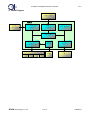
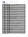
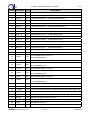
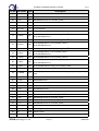
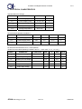
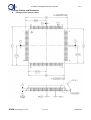
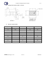
JL2005C
VGA Digital Camera
Controller
Revision: 1.0
Date: 8/18/2005
JEILIN Technology Co., Ltd.
8F, No.179, Jian Yi Rd., Chung Ho,
Taipei Hsien, Taiwan
TEL:886-2-82215466
FAX:886-2-82215456
JL2005C VGA Digital Camera Controller
V1.0
Table of Contents
0.
REVISION HISTORY................................................................................................................3
1.
GENERAL DESCRIPTION......................................................................................................4
2.
FEATURES ................................................................................................................................4
3.
APPLICATION...........................................................................................................................4
4.
BLOCK DIAGRAM ...................................................................................................................5
5.
PIN DESCRIPTIONS................................................................................................................6
6.
ELECTRICAL CHARATERISTICS ......................................................................................10
7.
PACKAGE OUTLINE AND DIMENSION............................................................................ 11
JEILIN Technology Co., Ltd.
2 of 13
2005/8/18
JL2005C VGA Digital Camera Controller
V1.0
0. Revision History
Revision
1.0
Description of Changes
First Release
JEILIN Technology Co., Ltd.
Date
2005/08/18
3 of 13
2005/8/18
JL2005C VGA Digital Camera Controller
V1.0
1. General Description
JL2005C is a low cost and highly integrated DSC controller. It consists of CMOS image sensor interface,
image processing, image compression engine, low battery detect, status LCD interface, DDR/SDRAM
interface, UART port and USB1.1 interface. JL2005C supports most popular VGA sensors. It provides
dual-mode operation, DSC mode and PC CAM mode. It is designed to fulfill the requirements of digital
camera applications.
The JL2005C integrates excellent image processing features such as AE, bad-pixel cancellation, image
compression engine. In DSC mode, it stores the compressed image data to an external SDRAM. In
PC-Camera mode, the compressed image data is downloaded to PC though USB interface.
2. Features
Dual mode operation
Supports CMOS image sensor with CIF, VGA resolution
Auto bad-pixel cancellation
AE measurement
Built-in compressed engine
Support 8/16-bit DDR/SDR SDRAM up to 128Mb (16Mb, 32Mb, 64Mb, 128Mb)
SDRAM chip test and downgrade SDRAM address remapping
Status LCD controller
Embedded turbo mode 8051 with ISP function
Built-in 24K bytes mask ROM
Supports external ROM
USB1.1 interface
Provides multi-function GPIOs
PWM waveform generator for mechanical shutter and flash light control
Low battery detect
100-pin LQFP package/COB (Chip On Board)
3. Application
Low Cost SDRAM DSC
Web CAM
PC CAM
JEILIN Technology Co., Ltd.
4 of 13
2005/8/18
JL2005C VGA Digital Camera Controller
V1.0
4. Block Diagram
SDRAM/DDR
JL2005C
CMOS Sensor
Interface
CMOS
Image Sensor
SDRAM
Controller
Image Processor
Bus Arbiter
Turbo mode
8051
(24KB mask ROM)
Voltage
Detector
USB1.1
Battery
PC
GPIO
Key
JEILIN Technology Co., Ltd.
Status
STN
Buzzer
Flash
Light
5 of 13
2005/8/18
JL2005C VGA Digital Camera Controller
V1.0
5. Pin Descriptions
Pin No. Pin Name Type
P
Description
1
VDD33_XSC
2
XSCI
ICLK Crystal oscillator pad input, connect to12 MHz crystal
3
XSCO
OCLK Crystal oscillator pad output, connect to12 MHz crystal
4
VSS33_XSC
5
/RESET
I, S
Power on reset, active low
6
S_PWDN
O2
CMOS image sensor power down signal
7
S_RESET
O2
CMOS image sensor reset signal
8
S_EXCLK
O2
CMOS image sensor system clock
9
S_PCLK
I
CMOS image sensor pixel clock
10
S_HSYNC
I
CMOS image sensor horizontal synchronous
11
S_VSYNC
I
CMOS image sensor vertical synchronous
12
S_D0
I
CMOS image sensor video data bus
13
S_D1
I
CMOS image sensor video data bus
14
S_D2
I
CMOS image sensor video data bus
15
S_D3
I
CMOS image sensor video data bus
16
S_D4
I
CMOS image sensor video data bus
17
S_D5
I
CMOS image sensor video data bus
18
S_D6
I
CMOS image sensor video data bus
19
S_D7
I
CMOS image sensor video data bus
20
SCL
OD
Serial clock output
21
SDA
OD
Serial data output
22
GPIO_0
B2
General purpose I/O 0 or Pattern generator 0 output *6
23
GPIO_1
B2
General purpose I/O 1 or Pattern generator 1 output *6
24
GPIO_2
B2
General purpose I/O 2 or External interrupt input, active low *6
25
GPIO_3
B2
General purpose I/O 3
26
GPIO_4
B2
General purpose I/O 4 or USB Plug-in input *6
27
GPIO_5
B2
General purpose I/O 5 or MPU data write enable output *6, active low
28
GPIO_6
B2
General purpose I/O 6
29
VCC2.5V
P
+2.5V core power
30
GND
G
Ground
31
VCC3.3V
P
+3.3V I/O power
32
GPIO_7
B2
General purpose I/O 7 or MPU program read enable output, active low *1
33
GPIO_8
B2
General purpose I/O 8 *1 or MPU program write enable output, active low
34
GPIO_9
B2
General purpose I/O 9 *1 or MPU Address latch enable output, active high
G
JEILIN Technology Co., Ltd.
+3.3V Crystal pad power
Crystal pad ground
6 of 13
2005/8/18
JL2005C VGA Digital Camera Controller
Pin No. Pin Name Type
35
36
GPIO_10
GPIO_11
B2
B2
Description
General purpose I/O 10
*1
or MPU address/data bit 0
General purpose I/O 11
*1
or MPU address/data bit 1
*1
or MPU address/data bit 2
37
GPIO_12
B2
General purpose I/O 12
38
GPIO_13
B2
General purpose I/O 13 *1 or MPU address/data bit 3
39
GPIO_14
B2
General purpose I/O 14 *1 or MPU address/data bit 4
40
GPIO_15
B2
General purpose I/O 15 *1 or MPU address/data bit 5
41
GPIO_16
B2
General purpose I/O 16 *1 or MPU address/data bit 6
42
GPIO_17
B2
General purpose I/O 17 *1 or MPU address/data bit 7
43
GPIO_18
B2
General purpose I/O 18 *1 or MPU address bit 8
44
GPIO_19
B2
General purpose I/O 19 *1 or MPU address bit 9
45
GPIO_20
B2
General purpose I/O 20 *1 or MPU address bit 10
46
GPIO_21
B2
General purpose I/O 21 *1 or MPU address bit 11
47
GPIO_22
B2
General purpose I/O 22 *1 or MPU address bit 12
48
GPIO_23
B2
General purpose I/O 23 *1 or MPU address bit 13
49
GPIO_24
B2
General purpose I/O 24 *1 or MPU address bit 14
50
GPIO_25
B2
General purpose I/O 25 *1 or MPU address bit 15
51
D_DQ0
B2
52
D_DQ1
B2
53
D_DQ2
B2
54
D_DQ3
B2
55
D_DQ4
B2
56
D_DQ5
B2
V1.0
16 bit SDRAM data bit 0 or Key_0 *2
8 bit SDRAM data bit 0
16 bit SDRAM data bit 1 or Key_1 *2
16 bit SDRAM data bit 2 or Key_2 *2
8 bit SDRAM data bit 1
16 bit SDRAM data bit 3 or Key_3 *2
16 bit SDRAM data bit 4 or Key_4 *2
8 bit SDRAM data bit 2
16 bit SDRAM data bit 5 or Key_5 *2
16 bit SDRAM data bit 6 or Key_6 *2
57
D_DQ6
B2
58
D_DQ7
B2
16 bit SDRAM data bit 7 or Key_7 *2
59
GPIO_26
B2
General purpose I/O 26 or DDR high byte data strobe output
60
D_LDQM
O2
DDR low byte data write mask or SDRAM low byte data input/output mask
61
/D_WE
O2
SDRAM write enable, active low
62
/D_CAS
O2
SDRAM column address strobe, active low
63
/D_RAS
O2
SDRAM raw address strobe, active low
64
D_BS0
O2
SDRAM bank address 0
65
D_BS1
O2
SDRAM bank address 1
66
D_A10
B2
SDRAM address bus or M51_nEA*5
JEILIN Technology Co., Ltd.
8 bit SDRAM data bit 3
7 of 13
2005/8/18
JL2005C VGA Digital Camera Controller
Pin No. Pin Name Type
Description
67
D_A0
B2
SDRAM address bus or Firmware_CFG0 *4
68
D_A1
B2
SDRAM address bus or Firmware_CFG1 *4
69
D_A2
B2
SDRAM address bus or Firmware_CFG2 *4
70
VCC2.5V
P
+2.5V core power
71
GND
G
Ground
72
VCC3.3V
P
+3.3V I/O power
73
D_A3
B2
SDRAM address bus or Firmware_CFG3 *4
74
D_DQ15
B2
75
D_DQ14
B2
76
D_DQ13
B2
77
D_DQ12
B2
78
D_DQ11
B2
79
D_DQ10
B2
16 bit SDRAM data bit 15 or Firmware_CFG15 *4
8 bit SDRAM data bit 7
16 bit SDRAM data bit 14 or Firmware_CFG14 *4
16 bit SDRAM data bit 13 or Firmware_CFG13 *4
8 bit SDRAM data bit 6
16 bit SDRAM data bit 12 or Firmware_CFG12 *4
16 bit SDRAM data bit 11 or Firmware_CFG11 *4
8 bit SDRAM data bit 5
16 bit SDRAM data bit 10 or Firmware_CFG10 *4
16 bit SDRAM data bit 9 or Firmware_CFG9 *4
80
D_DQ9
B2
81
D_DQ8
B2
16 bit SDRAM data bit 8: DQ_8 or Firmware_CFG8 *4
82
GPIO_27
B2
General purpose I/O 26 or DDR low byte data strobe output
83
D_UDQM
O2
84
/D_CLK
O2
DDR inverted clock
85
D_CLK
O2
DDR/SDRAM clock
86
D_CKE
O2
SDRAM clock enable
87
D_A11
B2
SDRAM address bus *3
88
D_A9
B2
SDRAM address bus *3
89
D_A8
B2
SDRAM address bus *3
90
D_A7
B2
SDRAM address bus or Firmware_CFG7 *4
91
D_A6
B2
SDRAM address bus or Firmware_CFG6 *4
92
D_A5
B2
SDRAM address bus or Firmware_CFG5 *4
93
D_A4
B2
SDRAM address bus or Firmware_CFG4 *4
94
VDD33_USB
P
+3.3V USB1.1 transceiver power
95
DM
USB USB D- signal
96
DP
USB USB D+ signal
97
VSS33_USB
G
JEILIN Technology Co., Ltd.
V1.0
8 bit SDRAM data bit 4
DDR high byte data write mask or SDRAM high byte data input/output
mask
USB1.1 transceiver ground
8 of 13
2005/8/18
JL2005C VGA Digital Camera Controller
Pin No. Pin Name Type
V1.0
Description
98
VDD25_PLL
P
+2.5V PLL and battery detect ADC power
99
VSS25_PLL
G
Ground for PLL and battery detect ADC
100
BAT_DET
AI
Low battery detect input
NOTE:
*1: This pin can be function as GPIO when internal mask ROM was enabled
*2: To prevent from disturbing normal SDRAM data access, please connect this pin to weak pull-up
and weak pull-down resistor for input Key function.
*3: Must pull-down this pin for normal operation.
*4: Signals on this pin will be latched to internal register when power on reset was active. After power
on reset was removed this pin will return to normal function as well.
*5: Pull-down this pin to select external ROM or pull-up this pin to select internal mask ROM.
*6: Each GPIO pin has it’s own function select register Alt, firmware can program each GPIO pin to
different function individually. It is as GPIO pin after power on reset.
Buffer Type Descriptions:
All CMOS input pin can take 5V tolerance
BUFFER
DESCRIPTION
I
3.3V CMOS Input pin
S
Schmitt-Trigger
B2
3.3V CMOS Bi-drectional pin with 2 mA drive
O2
3.3V CMOS Output pin with 2 mA drive
OD
3.3V CMOS Output pin with open drain
ICLK
XTAL clock input
OCLK
XTAL clock output
AI
USB
Analog input
USB Interface
P
Power pin
G
Ground pin
JEILIN Technology Co., Ltd.
9 of 13
2005/8/18
JL2005C VGA Digital Camera Controller
V1.0
6. ELECTRICAL CHARATERISTICS
Absolute Maximum Ratings
SYMBOL
PARAMETER
RATING
UNITS
VCC
Power Supply (3.3V)
-0.3 to 3.6
V
VCC1
Power Supply (2.5V)
-0.3 to 2.75
V
VIN
Input Voltage
-0.3 to VCC+0.3
V
VOUT
Output Voltage
-0.3 to VCC+0.3
V
TSTG
Storage Temperature
-55 to 150
℃
Recommended Operation Conditions
SYMBOL
PARAMETER
MIN
TYP
MAX
UNITS
VCC
Power Supply (3.3V)
3.0
3.3
3.6
V
VCC1
Power Supply (2.5V)
2.25
2.5
2.75
V
TOPR
Operating Temperature
0
25
70
℃
DC Electrical Characteristics for 3.3 volts operation
(Under Recommended Operating Conditions and VCC = 3.0V~3.6V, Tj = 0℃ to +70℃)
SYMBOL
PARAMETER
CONDITIONS
MIN
TYP
MAX
UNITS
VIL
Input Low Voltage
-0.3
0.8
V
VIH
Input High Voltage
2.0
Vcc+0.3
V
VT-
Schmitt Input Low Voltage
-0.3
0.8
V
VT+
Schmitt Input High Voltage
2.0
Vcc+0.3
V
VOL
Output Low Voltage
0.4
V
VOH
Output High Voltage
JEILIN Technology Co., Ltd.
2.4
10 of 13
V
2005/8/18
JL2005C VGA Digital Camera Controller
V1.0
7. Package Outline and Dimension
Package Outline (100-pin LQFP)
JEILIN Technology Co., Ltd.
11 of 13
2005/8/18
JL2005C VGA Digital Camera Controller
V1.0
Package Outline (100-pin LQFP) - continued
DETAIL F
SECTION G-G
Dimension (100-pin LQFP)
Symbol
Min
Nom
Max
Unit
A
-
-
1.6
mm
A1
0.05
0.15
mm
A2
1.35
1.45
mm
c
0.09
0.20
mm
b
0.17
0.2
0.27
mm
D
-
16
-
mm
D1
-
14
-
mm
e
-
0.5
-
mm
E
-
16
-
mm
E1
-
14
-
mm
L1
-
1
-
mm
JEILIN Technology Co., Ltd.
1.40
12 of 13
2005/8/18
JL2005C VGA Digital Camera Controller
V1.0
JEILIN Technology Co., Ltd.
8F, No. 179, Jian Yi Rd., Chung Ho,
Taipei Hsien, Taiwan
Tel: 886-2-8221-5466
Fax: 886-2-8221-5456
Website: www.jeilin.com.tw
Email: [email protected]
©2005 JEILIN Technology Corp., Ltd. All rights reserved.
The information in this document has been carefully checked and is believed to be reliable;
however no responsibility can be assumed for inaccuracies that may not have been caught. All
information in this document is subject to change without prior notice. The information
contained in this document is presented only as a guide for applications of our products. No
responsibility is assumed by JEILIN Technology for any infringements of intellectual property or
other rights of the third parties, which may result from its use. No license is granted by
implication or otherwise under any intellectual property or other rights of JEILIN Technology or
others. No part of this document may be reproduced in any form, in an electronic retrieval
system or otherwise, without the prior written permission of JEILIN Technology.
JEILIN Technology Co., Ltd.
13 of 13
2005/8/18