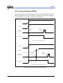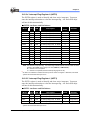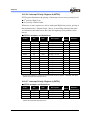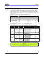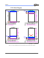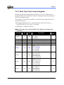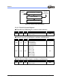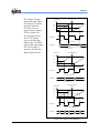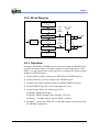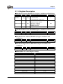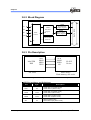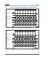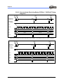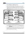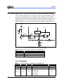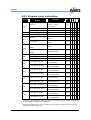
1
eSL/eSLS Series (+ eSLZ000) 16 Bits DSP Sound Processor USER’S MANUAL Doc. Version 1.7 ELAN MICROELECTRONICS CORP. December 2009 Trademark Acknowledgments: IBM is a registered trademark and PS/2 is a trademark of IBM Windows is a trademark of Microsoft Corporation ELAN and ELAN logo are trademarks of ELAN Microelectronics Corporation Copyright © 2006 ~ 2009 by ELAN Microelectronics Corporation All Rights Reserved Printed in Taiwan The contents of this User’s Manual (publication) are subject to change without further notice. ELAN Microelectronics assumes no responsibility concerning the accuracy, adequacy, or completeness of this publication. ELAN Microelectronics makes no commitment to update, or to keep current the information and material contained in this publication. Such information and material may change to conform to each confirmed order. In no event shall ELAN Microelectronics be made responsible for any claims attributed to errors, omissions, or other inaccuracies in the information or material contained in this publication. ELAN Microelectronics shall not be liable for direct, indirect, special incidental, or consequential damages arising from the use of such information or material. The software (if any) described in this publication is furnished under a license or nondisclosure agreement, and may be used or copied only in accordance with the terms of such agreement. ELAN Microelectronics products are not intended for use in life support appliances, devices, or systems. Use of ELAN Microelectronics product in such applications is not supported and is prohibited. NO PART OF THIS PUBLICATION MAY BE REPRODUCED OR TRANSMITTED IN ANY FORM OR BY ANY MEANS WITHOUT THE EXPRESSED WRITTEN PERMISSION OF ELAN MICROELECTRONICS. ELAN MICROELECTRONICS CORPORATION Headquarters: Hong Kong: USA: No. 12, Innovation Road 1 Hsinchu Science Park Hsinchu, Taiwan 30077 Tel: +886 3 563-9977 Fax: +886 3 563-9966 http://www.emc.com.tw Elan (HK) Microelectronics Corporation, Ltd. Flat A, 19/F, World Tech Centre 95 How Ming Street, Kwun Tong Kowloon , HONG KONG Tel: +852 2723-3376 Fax: +852 2723-7780 [email protected] Elan Information Technology Group (USA) Shenzhen: Shanghai: Elan Microelectronics Shenzhen, Ltd. Elan Microelectronics Shanghai, Ltd. 3F, SSMEC Bldg., Gaoxin S. Ave. I Shenzhen Hi-tech Industrial Park (South Area), Shenzhen, CHINA Tel: +86 755 2601-0565 Fax: +86 755 2601-0500 23/Bldg. #115 Lane 572, Bibo Road Zhangjiang Hi-Tech Park Shanghai, CHINA Tel: +86 21 5080-3866 Fax: +86 21 5080-4600 1821 Saratoga Ave., Suite 250 Saratoga, CA 95070 USA Tel: +1 408 366-8225 Fax: +1 408 366-8220 Contents Contents Contents iii Chapter 1 1 Introduction 1 1.1 Introduction to eSL/eSLS Series and eSLZ000 ICs...................................................1 1.2 Features .....................................................................................................................2 1.3 Parts List and Properties ............................................................................................3 1.3.1 eSLZ000 and eSL ICs Parts List and Properties.............................................3 1.3.2 eSLS ICs Parts List and Properties ..................................................................4 1.3.3 Properties Comparison between eSLZ000, eSL, and eSLS ICs .....................5 1.4 Algorithm Selection Table .........................................................................................6 1.4.1 eSLZ000 and eSL ICs Parts List and Properties.............................................6 1.4.2 eSLS ICs Parts List and Properties ..................................................................8 1.5 Typical Applications..................................................................................................9 1.6 Pin Descriptions ......................................................................................................10 1.6.1 Power Supply ................................................................................................10 1.6.2 System Control.............................................................................................. 11 1.6.3 DAC Output .................................................................................................. 11 1.6.4 Two Stage Amplifier & Touch Pad Positioning (Supports eSL and eSLZ000 ICs only) ................................................................................................................... 11 1.6.5 I/O Port..........................................................................................................12 1.6.6 Data ROM Interface (eSLZ000 only) ...........................................................14 1.6.7 ICE Interface (eSLZ000 only) ......................................................................14 Chapter 2 17 Architecture 17 2.1 eSL System Block Diagram ....................................................................................17 2.2 Program ROM and Data RAM Description............................................................18 2.2.1 Program ROM/RAM.......................................................................................18 2.2.2 Data RAM and Bank Select Register ..............................................................19 2.3 Addressing Modes....................................................................................................20 2.3.1 Register Direct Addressing ...........................................................................20 2.3.2 Register Indirect Addressing.........................................................................20 eSL/eSLS Series (+ eSLZ000) User’s Manual Contents • iii Contents 2.3.3 Indirect Addressing with Post-Decrement ....................................................21 2.3.4 Indirect Addressing with Post-Increment......................................................21 2.3.5 I/O Direct Addressing ...................................................................................21 2.3.6 RAM (Data) Direct Addressing ....................................................................22 2.3.7 Immediate Addressing ..................................................................................23 2.3.8 Relative Program Addressing .......................................................................23 2.3.9 Data Indirect Addressing with Displacement ...............................................24 2.4 Register Architecture................................................................................................25 2.4.1 General Purpose Registers ............................................................................26 2.4.2 Program Counter (PC) ..................................................................................26 2.4.3 Stack Pointer (SP) .........................................................................................26 2.4.4 Repeat and Loop Registers ...........................................................................26 2.4.5 Status Register (SR) ......................................................................................27 2.5 Instruction Set ..........................................................................................................29 2.5.1 Logic and Mathematic Instructions ..............................................................30 2.5.2 Conditional Branch Instruction.....................................................................31 2.5.3 Shift and Rotation Instructions .....................................................................32 2.5.4 Data Transfer Instruction ..............................................................................33 2.5.5 Bit Operation Instruction ..............................................................................34 2.5.6 Control Instructions ......................................................................................35 2.5.7 DSP Instruction .............................................................................................36 2.6 Power Supply Circuit ...............................................................................................39 2.6.1 Power Supply Attributes and Features ..........................................................39 2.7 Oscillator System .....................................................................................................40 2.7.1 Block Diagram ..............................................................................................40 2.7.2 Operation.......................................................................................................41 2.7.3 CPU Control Registers..................................................................................44 2.8 Reset System ...........................................................................................................44 2.8.1 Block Diagram ..............................................................................................45 2.8.2 Operation.......................................................................................................46 2.8.3 Power-On Reset (POR).................................................................................47 2.8.4 Brown-Out Reset (BOR)...............................................................................48 2.9 System Mode Operation...........................................................................................49 2.9.1 Block Diagram ..............................................................................................49 2.9.2 Operation.......................................................................................................49 2.9.4 Registers........................................................................................................50 2.9.5 System Mode Operation Examples...............................................................51 2.10 Exception-Handling .................................................................................................51 2.10.1 Reset..............................................................................................................51 2.10.2 Trap Instruction (TRAP)...............................................................................51 2.10.3 Interrupts .......................................................................................................51 2.11 External Interrupt ....................................................................................................57 2.11.1 External Interrupt Control Register ..............................................................57 iv • Contents eSL/eSLS Series (+ eSLZ000) User’s Manual Contents 2.11.2 Application Examples...................................................................................58 2.12 Stack Pointer Limit (SPLIM)..................................................................................59 2.12.1 General Description......................................................................................59 2.12.2 Block Diagram .............................................................................................60 2.12.3 Register Description .....................................................................................61 2.12.4 Operation Description ..................................................................................61 Chapter 3 63 Peripheral Control 63 3.1 Watchdog Timer (WDT) .........................................................................................63 3.1.1 Block Diagram ..............................................................................................64 3.1.2 Watchdog Control Register...........................................................................64 3.1.3 Examples ........................................................................................................65 3.2 Real Time Clock (RTC) ..........................................................................................66 3.2.1 Real Time Clock and Interrupt Block Diagram ............................................66 3.2.2 Real Time Clock Control Register................................................................67 3.2.3 RTC Timing....................................................................................................68 3.2.4 Examples.......................................................................................................70 3.3 Timer .......................................................................................................................71 3.3.1 Timer 0/1.......................................................................................................71 3.3.2 Timer 2/3.......................................................................................................74 3.4 Pulse Width Modulation (PWM) .............................................................................84 3.4.1 Features .........................................................................................................84 3.4.2 Block Diagram ..............................................................................................85 3.4.3 Operation.......................................................................................................85 3.4.4 Registers........................................................................................................87 3.4.5 Examples.......................................................................................................89 3.5 Digital to Analog Converter (DAC)........................................................................90 3.5.1 Features .........................................................................................................90 3.5.2 Operation.......................................................................................................90 3.5.3 Registers........................................................................................................90 3.5.4 Application Example ....................................................................................91 3.5.5 Examples.......................................................................................................91 3.6 Analog to Digital Converter (eSL and eSLZ000 only) ............................................92 3.6.1 Features .........................................................................................................93 3.6.2 Registers........................................................................................................93 3.6.3 Operation.......................................................................................................95 3.6.4 Examples.......................................................................................................97 3.7 Data ROM ..............................................................................................................100 3.7.1 Features .......................................................................................................100 eSL/eSLS Series (+ eSLZ000) User’s Manual Contents • v Contents 3.7.2 Block Diagram ............................................................................................100 3.7.3 Register Description....................................................................................101 3.7.4 Examples.....................................................................................................102 3.8 Serial Peripheral Interface (eSL and eSLZ000 only) .............................................104 3.8.1 Features .......................................................................................................104 3.8.2 Block Diagram ............................................................................................106 3.8.3 Pin Description............................................................................................106 3.8.4 SPI Register ................................................................................................109 3.8.5 SPI Transfer Format.................................................................................... 111 3.8.6 SPI Timing Diagrams.................................................................................. 112 3.8.7 Master Mode Operation .............................................................................. 115 3.8.8 Slave Mode Operation ................................................................................ 116 3.8.9 SPI Master Initial Flow Chart ..................................................................... 117 3.8.10 SPI Boot Flash (Interface) and SPI Data Flash (Interface) ...................... 117 3.8.11 Examples..................................................................................................... 118 3.9 Microphone Front End (eSL and eSLZ000 only) ................................................... 119 3.9.1 Registers...................................................................................................... 119 3.9.2 Examples .....................................................................................................122 3.10 I/O Pad Architecture .............................................................................................123 3.10.1 CMOS Pad Cofiguration Diagrams............................................................124 3.11 General Purpose Input Output ..............................................................................128 3.11.1 Features.......................................................................................................128 3.11.2 I/O Port Register Descriptions ...................................................................129 3.11.3 Input Mode with Pull Up Resistor Delay Time..........................................132 3.11.4 I/O Port Application Examples...................................................................132 3.12 Voltage Regulator 5V / 3V....................................................................................134 Chapter 4 137 Electrical Electrical Characteristics 137 4.1 CPU Voltage – Frequency Graph ..........................................................................137 4.2 Absolute Maximum Ratings..................................................................................138 4.2.1 eSL and eSLS..............................................................................................138 4.2.2 eSLZ000......................................................................................................138 4.3 DC Characteristics ................................................................................................139 4.3.1 For eSL, eSLS and eSLZ000 ......................................................................139 4.3.2 For eSL and eSLS Only ..............................................................................140 4.3.3 For eSLZ000 Only ......................................................................................141 Chapter 5 vi • Contents 143 eSL/eSLS Series (+ eSLZ000) User’s Manual Contents Application Circuits 143 5.1 eSL Application Circuit ..........................................................................................143 5.2 eSLS Application Circuit ........................................................................................144 5.3 eSLZ000 Application Circuit..................................................................................145 Chapter 6 147 Instruction Set Summary 147 6.1 Symbol Summary..................................................................................................147 6.1.1 General Symbol ..........................................................................................147 6.1.2 Operand.......................................................................................................147 6.1.3 Operator ......................................................................................................148 6.1.4 Flag status (SR)...........................................................................................148 6.1.4 Operation Explainations..............................................................................148 6.2 Instruction Set Tables ............................................................................................149 6.2.1 Data Transfer Instructions...........................................................................149 6.2.2 Arithmetic Operation Instructions ..............................................................150 6.2.3 Logic Operation Instructions ......................................................................152 6.2.4 Bit Operation Instructions* .........................................................................153 6.2.5 Program Jump Instructions .........................................................................154 Appendix 157 eSL and eSLZ000 Special Function Registers 157 A.1 List of eSL & eSLZ000 Special Function Registers ..............................................157 A.2 List of eSLS Special Function Registers...............................................................159 Appendix 161 Flash Memory Compatibility List 161 A.1 List of eSL & eSLZ000 Flash Memory Compatibility ..........................................161 eSL/eSLS Series (+ eSLZ000) User’s Manual Contents • vii Contents viii • Contents eSL/eSLS Series (+ eSLZ000) User’s Manual Contents User’s Manual Revision History Doc. Version Revision Description Date 1.0 Official Version Release with following changes: • Revised ADC Timing Diagram in Section 3.6.3 • Revised MOV description in Section 4.5.2 • Add clock system description in Section 2.5 • Add interrupt description in Section 2.8.3 • Revised SPI description in Section 3.4 • Revised Opening Temperature Range in Section 4.1.2 2006/12/11 1.1 Revised Appliation circuits in Section 4.2.2 Add comment in Section 4.3.2 Modified OSCO in Section 2.7.2.1 Add comment in Selection table in Section 1.3.1 Modified Boot SPI in Section 1.3.3 Add RTC timing information in Section 3.2 Modified interrupt vector address width in Section 2.10.3 Modified description and figure in Section 2.12 Modified layout hierarchy in Section 4 Modified the Sampleing Rate Range in Section 1.3.1 Added the IOVDD, IOVSS, AVDD, AVSS in Section 1.5.1 2007/03/26 1.2 Modified long MOV instruction description in Section 6.2.1 Modified DROM code example in Section 3.7.4 Added eSL032 Modified SPI transmitter/receiver only in Section 3.8.7 and 3.8.8 Modified the Temperature Range in Section 4.2 Modified the Power supply voltage in Section 4.3.1 Modified the example in Section 3.6.4 and 3.5.5 Modified the IP attributes and definiations in Section 3 Added algorithm support such as beat tracking, sound location, speech control, pitch control in Section 1.2 and 1.3 Added the note about power optimization in Section 2.9.2 and 3.4.4 Added ADC input resistance and capacitance in Section 3.6 2007/08/10 1.3 Added package information in Section 1.3 Modified PWMP and PWMD initial value in Section 3.4.4 Modified Application Circuit in Section 5 Modified Figure number in Section 3.10 2007/11/10 1.4 SPI serial clock consideration in Section 3.8.3.1 and 3.8.8 Modified PWM current in Section 4.3 Modified BSR description in Section 2.2.2 Modified data direct address mode in Section 2.3.6 Modified mov instruction in Section 2.5.4.1 Added PortC DC characteristic in Section 4.1.3 2008/01/10 1.5 Modify LSA, LEA initlal value in Appendix Modify Application Circuit diagram in Section 5 Added EXINT wake-up comment in Section 2.11 Added FSR change comment in Section2.7.2 Add Regulator comment in Section 3.12 Added flash memory support table in Appendix Modified Algorithm support in Section 1.2 and 1.3 2008/10/15 eSL/eSLS Series (+ eSLZ000) User’s Manual Contents • ix Contents Modified Regulator comment in Section 3.12 and Section 5 x • Contents 1.6 Modify WDT example in Section 3.1.3 Modify Definition of TCNT2 and TCNT3 in Appendix A Added Algorithm-related section in Section 1.4 2009/04/15 1.7 Modify DROM example code in Section 3.7.4 Modify PC[7:0] pull-up resister in Section 4.3.1 Added ADC convertion time in Section 3.6.2 Added ADC enable timing in Section 3.6.2 2009/12/01 eSL/eSLS Series (+ eSLZ000) User’s Manual Contents eSL/eSLS Series (+ eSLZ000) User’s Manual Contents • xi Chapter 1 Chapter 1 Introduction 1.1 Introduction to eSL/eSLS Series and eSLZ000 ICs The eSL/eSLS Series and eSLZ000 ICs (or “eSL Series” for short) differ from each other in the following manner: eSL ICs fully comply with all features of the eSL Series. eSLS ICs is the simplified version of the eSL ICs. Hence, these chips have simpler performance than the eSL ICs. eSLZ000 IC is the eSLZ000 ICE kernel chip used to emulate the eSL/eSLS Series. ELAN eSL Series ICs are 16-bit DSP Sound Processor with multi-channel speech and instrument playback based on Elan 16-bit DSP platform. The series has a powerful 16-bit DSP architecture that handles most of the speech/melody functions. Speech and melody can be played back simultaneously with the speech synthesis implemented by software. A wide range of compression bit rates and various volume levels are supported. eSL Series chips are equipped with real instrument waveform which enable the chips to obtain good quality melody. ELAN eSL peripherals include RTC, Timer, WDT, DAC, PWM, etc. The eSL Series ICs offer FAST, SLEEP, GREEN, and SLOW modes of operation. The use of GREEN and SLOW mode further reduces power consumption. Moreover, GREEN mode also provides RTC function for wake-up propose. The chips are designed as a cost effective processors offering optimized performance and are ideal for such applications as high compression rate digital voice signal, high quality instrument melody, voice recognition, digital sound effect, etc. The eSL Series constructive features motivate exploration into wide variety of new creative ideas for more innovative products. ELAN eSL Series perform extremely well in speech application based on powerful DSP architecture and are endowed with good algorithm for audio compression. eSL/eSLS Series (+ eSLZ000) User’s Manual Introduction • 1 Chapter 1 1.2 Features MCU • 16-bit RISC CPU architecture • CPU clock: 20MHz @ 3.3V (eSL and eSLS only) • CPU clock: 18MHz @ 3.3V (eSLZ000 only) • Programmable PLL • 4 CPU operation modes (Fast, Slow, Green, & Sleep) • Powerful DSP Instruction Set (MAC, DIV, RPT, LOOP) • Saturation mode supported • 8 general purpose registers (GPR) • 20 interrupt sources with 2-level priority (eSL and eSLZ000 only) • 17 interrupt source with 2-level priority (eSLS only) Memory • 32K-word program memory • 2K-word data RAM (eSL and eSLS only) • 8K-word data RAM (eSLZ000 only) • 32/128/256/512K-word data ROM (eSL only) • 128/256/512K-word data ROM (eSLS only) • External data ROM up to 32MB (eSLZ000 only) Peripherals • Real Time Clock (RTC) with wake up function • Four 8-bit timers, two general purpose timer, two multiple-function timer • 8-bit Watch Dog Timer (WDT) with general purpose timer capability • 40 GPIO + 8 Output (eSL and eSLZ000 only) • 24 GPIO (eSLS only) • Serial Peripheral Interface (eSL and eSLZ000 only) • 12-bit Analog to Digital Converter with touch panel and MIC inputs (eSL and eSLZ000 only) • Built-in regulator • 12-bit current-steering Digital to Analog Converter (DAC) • 10-bit resolution Pulse Width Modulation (PWM) 2 • Introduction eSL/eSLS Series (+ eSLZ000) User’s Manual Chapter 1 1.3 Parts List and Properties 1.3.1 eSLZ000 and eSL ICs Parts List and Properties eSLZ000 eSL032 eSL128 eSL256 eSL512 eSL032 A/B* eSL128 A/B* eSL256 A/B* eSL512 A/B/C* 138 81 81 81 81 81 81 81 81 32K *16 (SRAM) 32K*16 32K*16 32K*16 32K*16 32K *16 32K *16 32K *16 32K *16 8K *16 2K *16 External Data ROM 32K * 16 (Up to 16M*16) 2K *16 2K *16 2K *16 2K *16 2K *16 2K *16 2K *16 128K*16 256K*16 512K*16 32K * 16 128K * 16 256K * 16 512K * 16 Product No. Pin Count Program ROM Data RAM 4*8-bit 4*8-bit 4*8-bit 4*8-bit 4*8-bit 4*8-bit 4*8-bit 4*8-bit 4*8-bit Yes Yes Yes Yes Yes Yes Yes Yes Yes PWM 10-bit 10-bit 10-bit 10-bit 10-bit 10-bit 10-bit 10-bit 10-bit Current D/A 12-bit 12-bit 12-bit 12-bit 12-bit 12-bit 12-bit 12-bit 12-bit A/D 12-bit 12-bit 12-bit 12-bit 12-bit 12-bit 12-bit 12-bit 12-bit SPI 1 sets 1 set 1 set 1 set 1 set 1 set 1 set 1 set 1 set Timer Watch Dog 40 I/O ports + 8 Output ports I/O * The product number with an “A,B,C” means the chip supports advanced audio algorithm. eSL/eSLS Series (+ eSLZ000) User’s Manual Introduction • 3 Chapter 1 1.3.2 eSLS ICs Parts List and Properties Product No. Pin Count Program ROM eSL128S eSL256S eSL512S eSL128SA* eSL256SA* eSL512SA* 45 45 45 45 45 45 32K *16 32K *16 32K *16 32K *16 32K *16 32K *16 Data RAM 2K *16 2K *16 2K *16 2K *16 2K *16 2K *16 Data ROM 128K * 16 256K * 16 512K * 16 128K * 16 256K * 16 512K * 16 4*8-bit 4*8-bit 4*8-bit 4*8-bit 4*8-bit 4*8-bit Timer Yes Yes Yes Yes Yes Yes PWM 10-bit 10-bit 10-bit 10-bit 10-bit 10-bit Current D/A 12-bit 12-bit 12-bit 12-bit 12-bit 12-bit Watch Dog I/O 24 I/O ports * The product number with an “A” means the chip supports advanced audio algorithm. 4 • Introduction eSL/eSLS Series (+ eSLZ000) User’s Manual Chapter 1 1.3.3 Properties Comparison between eSLZ000, eSL, and eSLS ICs Product No. eSLZ000 eSL eSLS JTAG ICE Yes No No Boot SPI Yes No No 48 48 24 (PortA + PortB0~7) Total I/O number Large Current I/O number 8+4 8+4 4 (PortA 12~15) Wake Up Pin 16+5 16+5 8+4 SPI Yes Yes No MIC Front-end AGC Yes Yes No ADC Yes Yes No eSL/eSLS Series (+ eSLZ000) User’s Manual Introduction • 5 Chapter 1 1.4 Algorithm Selection Table The ELAN eSL Series algorithm feature • • • • • • • • • • • • • Built-in software voice synthesizer (0.8K ~ 96Kbps@8kHz) Multiple flash with volume level option Control port output value directly by waveform (waveform control port) Support mark number in waveform with ROM optimized configuation Up to 2-channel speech with different channel sample rate or 1-channel speech + 8-channel melody Voice recording in 12, 16, 20, and 32 Kbps@8KHz Support beat tracking function to detect music tempo Support speed control to adjust playback speed Support pitch control to change voice pitch Support sound source detection function to detect the angle of sound position Support speaker dependent recognition to recognize voice command & control function which is dependent on speaker Support speaker independent recognition to recognize voice command & control function which is independent on speaker Support handwriting recognition engine to recognize characters, numeral, symbols, and gestures. 1.4.1 eSLZ000 and eSL ICs Parts List and Properties Product No. Audio** eSL032 eSL128 eSL256 Up to 2-channel speech with different channel sample rate or 1-channel speech + 8-channel melody Coding Type** 12K/16K/20K/32K/40K/48K/96K bps @ 8KHz Sampling Rate Range** 6kHz ~ 48KHz Recording 6 • Introduction eSL512 Yes eSL/eSLS Series (+ eSLZ000) User’s Manual Chapter 1 Product No. eSL032A* eSL128A* eSL256A* eSL512A* eSL032B* eSL128B* eSL256B* eSL512B* eSL512C* Up to 2-channel speech with different channel sample rate or 1-channel speech + 8-channel melody Audio** 12K/16K/20K Coding Type** /32K/40K 0.8K~96K bps @ 8KHz /48K/96K bps @8KHz Sampling Rate Range** 6kHz ~ 48KHz Recording Yes Yes Yes Yes Yes Yes Yes Yes No Beat Tracking Yes Yes Yes Yes Yes Yes Yes Yes No Speaker Independent Recognition No No No No Yes Yes Yes Yes No Speaker Dependent Recognition No No No No Yes Yes Yes Yes No Recording Yes Yes Yes Yes Yes Yes Yes Yes No Sound Source Detection Yes Yes Yes Yes Yes Yes Yes Yes No Speech Speed/Pitch Control Yes Yes Yes Yes Yes Yes Yes Yes Yes Hand Writing Recognition No No No No No No No No Yes eSL/eSLS Series (+ eSLZ000) User’s Manual Introduction • 7 Chapter 1 1.4.2 eSLS ICs Parts List and Properties Product No. Audio** eSL128S Audio** eSL512S UP to 2-channel speech with different channel sample rate or 1-channel speech + 8-channel melody Coding Type** Sampling Rate Range** Product No. eSL256S 12K/16K/20K/24K/32K/40K/96K bps @8KHz 6KHz ~ 48KHz eSL128SA* eSL256SA* eSL512SA* UP to 2-channel speech with different channel sample rate or 1-channel speech + 8-channel melody Coding Type** Sampling Rate Range** Speech Speed/Pitch Control 0.8K~96K bps @8kHz 6KHz ~ 48KHz Yes * The product number with an “A,B,C” means the chip supports advanced algorithm. A series support vocal high compress application. B series support vocie recognition (SI/SD) application, C series support hand write recognition (HWR) application. ** For further details, refer to the pertinent eSL Series Assembler Reference Guide, eSL Series C Macro Reference Guide and related Application note. 8 • Introduction eSL/eSLS Series (+ eSLZ000) User’s Manual Chapter 1 1.5 Typical Applications Long Duration Speech and Melody Playback Voice Recognition Education Learning Products Recording and Playback Products Intelligent Interactive Talking Toys Caller ID (DTMF/FSK decoder) Power Conversion and Motor Control General Purpose Controller eSL/eSLS Series (+ eSLZ000) User’s Manual Introduction • 9 Chapter 1 1.6 Pin Descriptions 1.6.1 Power Supply Refer to Section 2.6, Power Supply Circuit for more detailed information. Type Supported Voltage VDD_CPU P 3V Positive power supply for CPU, digital peripheral and DRAM VDD_PM P 3V Positive power supply for PROM, DROM and POR (eSL and eSLS only) Positive power supply for PRAM and POR (eSLZ000 only) VDD_OSC P 3V Positive power supply for Oscillator system and PLL VDD_ICE P 3V Positive power supply for DROM, ICE function and boot function I/O pad (eSLZ000 only) IOVDD_PWM P 3V, 5V Positive power supply for PortD and PWM I/O pad (eSL and eSLZ000 only) Positive power supply for PWM I/O pad(eSLS Seies only) IOVDD_PB P 3V, 5V Positive power supply for PortA.2~15 and PortB I/O pad IOVDD_PC P 3V, 5V Positive power supply for PortC I/O pad (eSL Series and eSLZ000) IOVDD* P 3V, 5V Positive power supply (eSLS Series only) VSS_CPU P 0V Negative power supply for CPU, digital peripheral and DRAM VSS_PM P 0V Negative power supply for PROM, DROM and POR (eSL and eSLS only) Negative power supply for PRAM and POR (eSLZ000 only) VSS_OSC P 0V Negative power supply for Oscillator system and PLL Name Description VSS_ICE P 0V Negative power supply for DROM, ICE function and boot function I/O pad (eSLZ000) IOVSS_PWM P 0V Negative power supply for PortD and PWM I/O pad (eSL and eSLZ000 only) Negative power supply for PWM I/O pad (eSLS only) IOVSS_PB P 0V Negative power supply for PortA.2~15 and PortB I/O pad IOVSS* P 0V Negative power supply (eSLS Series only) IOVSS_PC P 0V Negative power supply for PortC I/O pad (eSL and eSLZ000 only) AVDD_AD P 3V Positive power supply for A/D (eSL and eSLZ000 only) AVDD_DA P 3V Positive power supply for D/A AVDD** P 3V Positive power supply (eSLS Series only) AVSS_AD P 0V Negative power supply for A/D (eSL Series and eSLZ000) AVSS_DA P 0V Negative power supply for D/A AVSS** P 0V Negative power supply (eSLS Series only) VREF P 3V External reference voltage input pin for A/D and MIC (eSL and eSLZ000 only) RVIN P 5V Regulator voltage input RVOUT P 3V Regulator voltage output 3.0V 10 • Introduction eSL/eSLS Series (+ eSLZ000) User’s Manual Chapter 1 *These power pins must connect to the same VDD and VSS as IOVDD_PB and IOVSS_PB ** These power pins must connect to the same VDD and VSS as AVDD_DA and AVSS_DA NOTE The AVDD_AD, VREF are analog voltage input that need to separate with other digital voltage input to reduce noise issue. For example, you can use on-chip regulator to be the analog voltage source. Or you can refer to development board reference circuit. 1.6.2 System Control Name Type Description I RSTB is the low active global reset input* TEST I Test mode select pin (High active). Internal pull down. For chip internal test only. Connected to VSS normally. OSCI I X’tal or RC oscillator connecting pin RC or X’tal selection is by OSCS pin OSCO O X’tal oscillator connecting pin RSTB OSCS I RC or X’tal selection. 0 = RC; 1=X’tal PLLC I PLL loop filter capacitor** * This pin has an internal pull-up 150KΩ resistor (refer to Chapter 5, Application Circuit) ** This pin must connect a 47nF capacitor to ground (refer to Chapter 5, Application Circuit) 1.6.3 DAC Output Name Type DACO O Description Current D/A output pin 1.6.4 Two Stage Amplifier & Touch Pad Positioning (Supports eSL and eSLZ000 ICs only) Name AMPO Type O Description Post-Amplifier output MIC I Microphone signal input (AC coupling from microphone signal). AGC I Automatic Level Control adjustment pin. Xn I Touch Pad positioning for X axis about negative voltage level Yn I Touch Pad positioning for Y axis about negative voltage level Xp/ADIN0 I Touch Pad positioning for X axis about positive voltage level Analog Input channel 0 Yp/ADIN1 I Touch Pad positioning for Y axis about positive voltage level Analog Input channel 1 eSL/eSLS Series (+ eSLZ000) User’s Manual Introduction • 11 Chapter 1 1.6.5 I/O Port 1.6.5.1 Port A Attributes and Definitions Name PA[0] PA[1] Function Type Description GPIO I/O General-purpose input and output function PWM0 O PWM output 0 GPIO I/O General-purpose input and output function PWM1 O PWM output 1 PA[2] GPIO I/O General-purpose input and output function PA[3] GPIO I/O General-purpose input and output function GPIO I/O TEXI2 I GPIO I/O PA[4] PA[5] General-purpose input and output function External timer 2 clock input General-purpose input and output function TEXI3 I PA[6] GPIO I/O General-purpose input and output function PA[7] GPIO I/O General-purpose input and output function PA[8] PA[9] PA[10] PA[11] External timer 3 clock input GPIO I/O General-purpose input and output function TCCP2 I/O Timer 2 capture input or compare output GPIO I/O General-purpose input and output function TCCP3 I/O Timer 3 capture input or compare output GPIO I/O EXINT0 GPIO EXINT1 I I/O I General-purpose input and output function External interrupt 0 input General-purpose input and output function External interrupt 1 input General-purpose input and output function with programmable high current GPIO I/O /SS* I GPIO I/O General-purpose input and output function with programmable high current MOSI* I/O SPI function (Master output / Slave input) with programmable high current GPIO I/O General-purpose input and output function with programmable high current MISO* I/O SPI function (Master input / Slave output) with programmable high current GPIO I/O General-purpose input and output function with programmable high current SCK* I/O SPI function (in Master Mode used as serial clock output and as serial clock input in Slave Mode) with programmable high current PA[12] PA[13] PA[14] PA[15] SPI function (in Slave Mode, used as chip select input and can be used as I/O pin in Master Mode) with programmable high current * NOT applicable to eSLS ICs 12 • Introduction eSL/eSLS Series (+ eSLZ000) User’s Manual Chapter 1 1.6.5.2 Port B Attributes and Definitions For eSL, eSLS, and eSLZ000: Name Function PB[7:0] GPIO Type I/O I Description General-purpose input and output function Wake-up function with programmable pull-up resistor For eSL and eSLZ000 only: Name Function PB[15:8] GPIO Type I/O I Description General-purpose input and output function Wake-up function with programmable pull-up resistor NOTE eSLS ICs cannot access PB[15:8] that are always high. 1.6.5.3 Port C Attributes and Definitions (eSL and eSLZ000 only) Name Function PC[1:0] GPIO PC[7:2] GPIO ADIN2~7 Type I/O I I/O Description General-purpose input and output function Input with programmable pull-up resistor General-purpose input and output function I Input with programmable pull-up resistor I Analog Input channels NOTE PORTC[7:2] shares pin with ADC input. There is no Schmitt Trigger Input when input is from PORTC[7:2]. eSL/eSLS Series (+ eSLZ000) User’s Manual Introduction • 13 Chapter 1 1.6.5.4 Port D Attributes and Definitions (eSL and eSLZ000 only) Name Function Type Description PD[0] GPO O General-purpose output function pin with high drive current (1 * Tg delay) * PD[1] GPO O General-purpose output function pin with high drive current (5 * Tg delay) * PD[2] GPO O General-purpose output function pin with high drive current (2 * Tg delay) * PD[3] GPO O General-purpose output function pin with high drive current (6 * Tg delay) * PD[4] GPO O General-purpose output function pin with high drive current (3 * Tg delay) * PD[5] GPO O General-purpose output function pin with high drive current (7 * Tg delay) * PD[6] GPO O General-purpose output function pin with high drive current (4 * Tg delay) * PD[7] GPO O General-purpose output function pin with high drive current (8 * Tg delay) * * Tg = 4 nano-second for low noise design consideration 1.6.6 Data ROM Interface (eSLZ000 only) Name Type DROMA[23:0] O External Data ROM memory address bus Description DROMD[15:0] I/O External Data ROM memory data bus WEB O External Data ROM write enable output RDB O External Data ROM read enable output CEB O External Data ROM chip select output 1.6.7 ICE Interface (eSLZ000 only) ICE Interface Attributes and Definitions: Name 14 • Introduction Type Description TDI I Test data input TDO O Test data output TCK I Test clock TMS I Test mode select eSL/eSLS Series (+ eSLZ000) User’s Manual Chapter 1 Boot Attributes and Definitions: Name Type Description BTSI I Boot serial input BTCS O Boot chip select BTSCLK O Boot clock BTSO O Boot serial output System Mode Attributes and Definition: Name Type Description SYSMOD[0] O System mode status display LSB SYSMOD[1] O System mode status display MSB ICEMOD I 0: Processor mode (boot external SPI flash to internal program memory) 1: ICE mode eSL/eSLS Series (+ eSLZ000) User’s Manual Introduction • 15 Chapter 2 Chapter 2 Architecture 2.1 eSL System Block Diagram As shown in the block diagram below, ELAN eSL Series (eSL/eSLS Series and eSLZ000) utilize a modified Harvard architecture in such a way that the memory is organized into two separated fields; Program ROM and Data RAM. As the memory is separated, the central processing units can read/write data at the same time. Furthermore, the I/O space has an independent address, i.e., the I/O-mapped I/O. The different configurations of each domain are explained in this chapter. Program Counter I/O Space (SFR) I/O Direct ADC Control Unit RAM Addressing IMM #16 DAC 17x17 Multiplier / Divider (+16 bit ALU) ALU Bus Bus INT I/O Instruction Decoder General Purpose Registers Data Reg Addressing Addressing ROM Port A~D PWM Timer RTC ACC D WDT Status Reg SPI RAM OSC/PLL Contol Signals Figure 2-1 ELAN eSL Series System Block Diagram. eSL/eSLS Series (+ eSLZ000) User’s Manual Architecture • 17 Chapter 2 2.2 Program ROM and Data RAM Description 2.2.1 Program ROM/RAM 18 • Architecture Program ROM/RAM Reset Vector 0x0000 0x0002 Short Call Interrupt Vector PC R0 0x3FFF Long Call It includes 32K * 16-bit on-chip ROM (for both eSL & eSLS Series) or RAM (eSLZ000 only) for your program and general data storage utilization. Program counter (PC) is the dedicated counter for program address, and is automatically modified by control flow processing. The eight general purpose registers can be used as Program ROM or RAM pointers. General Purpose Registers (Indirect pointer) Total 32K * 16-bit Linear memory space R7 0x7FFF (32767) 16-bit Figure 2-2 eSL Series Program ROM Block Diagram eSL/eSLS Series (+ eSLZ000) User’s Manual Chapter 2 2.2.2 Data RAM and Bank Select Register The Figure 2-3 at right shows the organization in the eSL data RAM. It consisted of six different addressing modes for the data memory cover, namely; • 16-bit direct • 8-bit direct, Indirect with Displacement, • Indirect, • Indirect with Post-decrement, and • Indirect with Post-increment. Data RAM 0x0000 0x00FF 0x0100 16 0x01FF 8-bit BSR 8-bit direct address 1 cycle instruction 16 16-bit direct address Total 2K * 16-bit Linear memory space 2cycle instruction R0 16 General Purpose Registers (Indirect pointer) R7 0x07FF * 0x1FFF * * 16-bit BSR (Bank Select Register) is used for MOV instruction. When user use 8-bit MOV instruction, they must make sure the BSR is correct. User doesn’t care the BSR if they use 16-bit MOV instruction (L). Please see the data transfer instruction and appendix about code optimization. eSL/eSLS Series (+ eSLZ000) User’s Manual * eSL & eSLS ** eSLZ000 only Figure 2-3 eSL Series Data RAM Block Diagram Architecture • 19 Chapter 2 2.3 Addressing Modes ELAN eSL Series supports powerful and efficient addressing modes. A lot of instructions use several addressing modes. The following sections will describe the available eSL Series addressing modes. 2.3.1 Register Direct Addressing The operands are in the register file. Example: R1 = R2 + R3 General Purpose Registers OP Rd Rs Rt R0 R7 Figure 2-4 Register Direct Addressing 2.3.2 Register Indirect Addressing Operand address is the contents of the registers used when accessing the RAM or ROM. Example: R3 = [R2] – R1 – B and R3 = P[R1] ROM/RAM Space General Purpose Register 0 65535 Figure 2-5 Register Indirect Addressing 20 • Architecture eSL/eSLS Series (+ eSLZ000) User’s Manual Chapter 2 2.3.3 Indirect Addressing with Post-Decrement The indirect register pointer is decremented by 1 after operation. Example: R3 = [R5--] and D = R5 * [R6--] (US). ROM/RAM Space General Purpose Register -1 0 + 65535 Figure 2-6 Indirect Addressing with Post-Decrement 2.3.4 Indirect Addressing with Post-Increment The indirect register pointer is incremented by 1 after operation. The addressing mode is very powerful for bulk operation and for operations that need a lot of memory accesses. The purpose of the addressing mode is to keep high MAC data path utilization. Example: D = D + [R3++] * P[R4++] and [R1++] = P[R5++] ROM/RAM Space General Purpose Register 1 0 + 65535 Figure 2-7 Indirect Addressing with Post-Increment 2.3.5 I/O Direct Addressing The address is contained in a 7-bit instruction word. The second operand is either Rd1 or Rs2 (destination or source register respectivley) used by IN and OUT instructions to read from or write to the I/O registers. 1 2 Rd is the Destination Register of General Purpose Registers. Rs is the Source Register of General Purpose Registers. eSL/eSLS Series (+ eSLZ000) User’s Manual Architecture • 21 Chapter 2 Example: R6 = IO[PORTA] and POP IO[PORTC] I/O Space OP I/O address 0 128 Figure 2-8 I/O Direct Addressing 2.3.6 RAM (Data) Direct Addressing An 8-bit data address is contained in the 1-word instruction. Rd or Rs specifies the destination or source register respectively. For example, R = RAM_bank A 16-bit data address is contained in the 16 LSBs of a 2-word instruction. Rd or Rs specifies the destination or source register respectively. Example: R = RAM8 RAM Space (Banked) OP RAM Direct Add. 0 256 Figure 2-9a RAM (8-Bit Data) Direct Addressing Example: R = RAM16 RAM Space OP Rd/Rs Direct Address 0 65535 Figure 2-9b RAM (16-Bit Data) Direct Addressing 22 • Architecture eSL/eSLS Series (+ eSLZ000) User’s Manual Chapter 2 2.3.7 Immediate Addressing A 16-bit program address is contained in the 16 LSBs of a 2-word instruction. Example: CALL label and JMP label ROM Space OP Absolute Address 0 65535 Figure 2-10 Immediate Addressing 2.3.8 Relative Program Addressing Program execution continues at Address PC + offset + 1. The offset is contained in the instruction word. Short conditional branch instructions can only get to locations –256 to 255 from the current address. However, Long Branch instructions can reach the entire program memory from every location. NOTE Long range condition branch can reach from 0 to 65,535, but it needs two-word instructions. ROM Space Program Counter 0 + OP Offset address 65535 Figure 2-11 Relative Program Addressing eSL/eSLS Series (+ eSLZ000) User’s Manual Architecture • 23 Chapter 2 2.3.9 Data Indirect Addressing with Displacement Operand address is the result of the register contents added to the address contained in 5 bits of the instruction word. For example, R1 = [R3 -#10]; R3 is the only register that can be the base register. Example: R1 = [R3 – #10] NOTE R3 is the only register available that can be used as base register 4 OP Rs 0 RAM Space Offset 0 + GPR 65535 Figure 2-12a Data Indirect with 5-Bit Displacement Addressing Operation Diagram Operand address is the result of the register contents added to another register. Example: [R3 – R1] = R2 NOTE R3 is the only register available that can be used as base register 2 OP 0 Rs Rt GPR GPR RAM Space 0 + 65535 Figure 2-12b Data Indirect with 5-Bit Displacement Addressing Operation Diagram 24 • Architecture eSL/eSLS Series (+ eSLZ000) User’s Manual Chapter 2 2.4 Register Architecture The following figure shows the ELAN eSL Series register architecture. Each of these Registers are discussed in details in the following pages. 1. Register Space regs G ENERAL PURPOSE REGISTER 15 0 R0 R1 R2 R3 R4 R5 R6 R7 R1 R0 ACCUM ULATOR D (D) 2. I/O Space regs 0 15 PRO GRAM COUNTER (PC) 0 15 STACK POINTER (SP) 0 15 REPEAT COUNTER (RC) 0 15 LO OP COUNTER (LC) 0 15 LO OP START ADDRESS (LSA) 0 15 LOOP END ADDRESS (LEA) 0 15 STATUS REGISTER (SR) 15 0 SPECIAL FUNCTION REGISTER (SFR) Note: ( ) means Register Notation Figure 2-13 ELAN eSL Series Register Organization eSL/eSLS Series (+ eSLZ000) User’s Manual Architecture • 25 Chapter 2 2.4.1 General Purpose Registers Register space consists of 8 x 16-bit General Purposes Registers. They are used as data, address, or offset registers. They can address up to 64 K addressing space (ROM, RAM) without any segmentation (bank). In addition to their general usage, the Registers R0 and R1 have some other functions. These two registers are treated as a single double-word (32-bit) accumulator called “Accumulator D” that hold operands and results of the arithmetic calculations or data manipulations such as division and multiplication. 2.4.2 Program Counter (PC) The Program Counter is a 16-bit wide register that holds the address of the next instruction to be executed. Therefore, the PC can address up to 64K instruction words (Read only). 2.4.3 Stack Pointer (SP) The Stack Pointer holds the 16-bit address of the last used stack location and is automatically modified by interrupt processing, subroutine calls, and returns. You may reprogram the SP during initialization to any location within data (RAM) space. The SP also can be used by in the user software (PUSH and POP instructions), but you should remember that the CPU also uses the SP. 2.4.4 Repeat and Loop Registers These Repeat and Loop Registers actually are made up of 4 registers; i.e., Repeat Counter, Loop Counter, Loop Start Address, and Loop End Address. They are used as temporary registers when executing repeat or loop instruction. The Repeat and Loop Counter stored the repeat time. Furthermore, it needs to store the start and end address in a loop operation. 26 • Architecture eSL/eSLS Series (+ eSLZ000) User’s Manual Chapter 2 2.4.5 Status Register (SR) The Status Register contains the following system status bits: Bit15 GIE X* x* x* x* 10 9 SME S6R 8 F/I x* x* x* 4 T 3 N 2 Z 1 V Bit0 C *x = Don’t care. Reserved for future enhancements Where: Carry (C) Flag: C is set when a carry or borrow occurs during an arithmetic operation. The Carry Flag bit is set or reset, depending on the operation that is performed. For ADD instructions C = 1: Carry occurs C = 0: No carry occurs For SUBTRACT instructions: C = 1: No borrow occurs C = 0: Borrow occurs For COMPARE instructions: Same as SUBTRACT instruction For ROTATION instructions: The Carry flag is used as a link between the least significant bit (LSB) and most significant bit (MSB). Overflow (V) Flag: V is set when a two complement overflows occurs as a result of an operation. V = 1: Overflow occurred V = 0: No overflow occurred Zero (Z) flag: The Z bit is set when all the resulting bits are 0s. Z = 1: The result equals zero after operation (R1:R0 = 0 when under MAC operation) Negative (N) Flag The negative flag stores the state of the most significant bit of the output result. N = 1: The result of the operation is negative. N = 0: The result of the operation is not negative. Test (T) Flag T is used by Bit test operation instruction (BTEST) T = 1: The tested bit is 1 T = 0: The tested bit is 0 eSL/eSLS Series (+ eSLZ000) User’s Manual Architecture • 27 Chapter 2 Fractional / Integer (F/I) Flag F/I is used to indicate Fractional or Integer mode F/I = 1: Fractional mode F/I = 0: Integer mode Shift 6 Bit (S6R) Flag S6R is used to indicate Shift 6 bit or otherwise S6R = 1: Right Shift 6 bit S6R = 0: Left Shift 0 bit (F/I = 0) Left Shift 1 bit (F/I = 1) Saturation Mode (SME) Flag SME is used to indicate Saturation mode status SME = 1: Saturation mode enabled SME = 0: Saturation mode disabled Global Interrupt Enable (GIE) Flag The Global Interrupt Enable bit must be set to “1” for the interrupts to be enabled. If reset, all maskable interrupts are disabled. The GIE bit is cleared by interrupts and restored by the RETI instruction. GIE = 1: Interrupts are enabled GIE = 0: Interrupts are disabled 2.4.5.1 Division and Multiplication Modes S6R F/ I 0 0 Integer Division Integer Multiplication 0 1 Fractional Fractional (Left Shift 1 bit) 1 0 Integer Right Shift 6 bit 1 1 Fractional Right Shift 6 bit 2.4.5.2 ALU Saturation Mode – 16bit 28 • Architecture SME Overflow (V) Carry (C) ALU Output 0 X X ALU Output 1 0 0 ALU Output 1 0 1 ALU Output 1 1 0 0111111111111111 1 1 1 1000000000000000 eSL/eSLS Series (+ eSLZ000) User’s Manual Chapter 2 2.4.5.3 MAC/MAS Saturation Mode – 32BIT SME Overflow (V) Carry (C) MAC Output 0 X X MAC Output 1 0 0 MAC Output 1 0 1 MAC Output 1 1 0 0X7FFFFFFF 1 1 1 0X80000000 2.5 Instruction Set There are two things which you must take note with the instruction set definitions. First, the to-be completed instruction set must have no missing functionality. Second, the instructions should be orthogonal, that is, they must not be redundant unnecessarily. ELAN eSL Series has a 16-bit instruction set (1 or 2 words). It is organized into instruction categories grouped by function as shown in the table below. There are only 60 instructions which make software development quite convenient. Function Groups Instructions Logic and Mathematic Instructions AND, OR, XOR, COM, NEG, CMP, CLR, ADD, ADC, SUB, SUBB, INC, DEC Branch Instructions JCC, JCS, JLS, JGE, (S)JMP, (L)JMP Shift Instructions SHL, SHR, ROL, ROR, ASR Data Transfer Instructions MOV [R = R; R.l = #8; R.h = #8; R = RAM[In,m]; R = ROM[In,m]; RAM[In,m] = R; R = RAMname; RAMname = R IN [R=IO <Add>]; OUT [IO <Add>=R] PUSH R;IO; POP R; IO; SWAP [R.h = R (Low Byte), R.l = R (High Byte)] Bit Operation Instructions BS, BC, BTEST, BTG IO; Register; RAM Control Instructions (S)CALL, (L)CALL, NOP, RET, RETI, RPT, LOOP, TRAP DSP Instructions MUL.UU, MUL.US, MUL.SU, MUL.SS, MAC, MAS, DIV, DIVS eSL/eSLS Series (+ eSLZ000) User’s Manual Architecture • 29 Chapter 2 2.5.1 Logic and Mathematic Instructions The eSL Series has a full set of 6-bit (1 word) and 16-bit (2 words) logic and mathematic instructions. WD General Purpose Registers 3 Rd Rs 3 3 Rt DBUS SC1 SC2 16 16 DBUS #16 "1" Negate ALU OP ALU 16 Status Register Figure 2.14 The ALU unit. Logic and Mathematic Instruction Definitions Mnemonic Operand Addition without carry Rn; [Rn]; #6imm; #16imm ADC Add with Carry Rn; [Rn]; #6imm; #16imm SUB Subtraction without borrow Rn; [Rn]; #6imm; #16imm Subtraction with borrow Rn; [Rn]; #6imm; #16imm Logical AND Rn; [Rn]; #6imm; #16imm SUBB AND OR 30 • Architecture Description ADD Logical OR Rn; [Rn]; #6imm; #16imm XOR Logical exclusive OR Rn; [Rn]; #6imm; #16imm CMP Compare Rn NEG 2’s complement Rn COM 1’s complement Rn eSL/eSLS Series (+ eSLZ000) User’s Manual Chapter 2 2.5.2 Conditional Branch Instruction Conditional jumps support program branching relative to the program counter. The numeric range of short condition branch is 9-bit offset values (-256 to 255). Long range condition branch can reach from 0 to 65,535, but it needs two words instruction. The condition branch instructions that are supported by the eSL are shown in the following table. When an specified condition is met, a signed 9-bit is added to the value in the program counter, or the program counter is replaced by 16-bit absolute address. Condition Branch Instruction Definitions Mnemonic Description Operation Comment IF CC JMP Jump if carry (C) clear If (C==0) then jump to PC +n+ 1 Simple IF CS JMP Jump if carry (C) set If (C==1) then jump to PC +n+ 1 Simple IF VC JMP Jump if overflow (V) clear If (V==0) then jump to PC +n+ 1 Simple IF VS JMP Jump if overflow (V) set If (V==1) then jump to PC +n+ 1 Simple IF NE JMP Jump if not equal If (Z==0) then jump to PC +n+ 1 Simple IF EQ JMP Jump if equal If (Z==1) then jump to PC +n+ 1 Simple IF PL JMP Jump if plus If (N==0) then jump to PC +n+ 1 Simple IF MI JMP Jump if minus If (N==1) then jump to PC +n+ 1 Simple IF TC JMP Jump if test (T) clear If (T==0) then jump to PC +n+ 1 Simple IF TS JMP Jump if test (T) set If (T==1) then jump to PC +n+ 1 Simple IF LO JMP Jump if lower than If (C==0) then jump to PC +n+ 1 Unsigned IF HS JMP Jump if higher or same If (C==1) then jump to PC +n+ 1 Unsigned IF LS JMP Jump if lower or same If (N^V==0) then jump to PC +n+ 1 Unsigned IF GE JMP Jump if greater than or equal If (N^V==1) then jump to PC +n+ 1 Signed IF GT JMP Jump if greater than If (Z|(N^V)==0) then jump to PC +n+ 1 Signed IF LE JMP Jump if less than or equal If (Z|(N^V)==1) then jump to PC +n+ 1 Signed IF LT JMP Jump if less than If (C==0 | Z==1) then jump to PC +n+ 1 Signed JMP Always Jump Always jump to PC +n+ 1 Simple The instruction code fetch and the program counter increment technique end with the following formula: • PC_new = PC_old + 1 + Offset (When taking a short branch) • PC_new = 16-bit (LSB) absolute address (When taking a long branch) NOTE Condition Branch can be used simply by keying the mnemonic. The eSL assembler chooses the short or long branch depending on the offset range status. eSL/eSLS Series (+ eSLZ000) User’s Manual Architecture • 31 Chapter 2 2.5.3 Shift and Rotation Instructions The Shift and Rotation instructions are general purpose registers. This Shift is capable of performing one bit shifting functions and the shifted-out bits are all passed through the C flag bit. The Rotation performs rotation operation though register and the C flag bit. Use arithmetic shift right (ASR) for keeping the sign bit. Shift and Rotation Instructions Definition Mnemonic Description SHL Shift Left SHR Shift Right ROL Rotate Left ROR Rotate Right ASR Arithmetic Shift Right 15 0 C 0 15 SHL 0 0 C 15 SHR 0 ROL C 15 0 ROR C 15 0 C ASR Figure 2.15 Shift Instructions Shifting Diagram 32 • Architecture eSL/eSLS Series (+ eSLZ000) User’s Manual Chapter 2 2.5.4 Data Transfer Instruction The Data Transfer instruction moves data from a source to a destination. It provides indirect auto-increase or decrease mode for moving large block of data around main memory. The following table lists the functions within the Data Transfer instruction. 2.5.4.1 Data Transfer Instruction Description Mnemonic 1 Description 1 MOV Move from RHS to LHS IN Input from I/O OUT Output to I/O PUSH Push to TOS POP Pop from TOS 2 3 RHS: Right hand side; 2 LHS: Left hand side; 3 TOS: Top of stack MOV instruction provides the data transfer ability to move data from memory to register (LOAD) or from register to memory (STORE). IN and OUT instructions are capable of moving data via I/O space, while PUSH and POP instructions provide a channel between register and stack (or I/O and stack). There are two kind data memory mov instruction, one is 8-bit mov instruction, user need to set BSR and 8-bit direct address to do the mov operation, the other is 16-bit long mov instruction, user just need to set 16-bit direct address. Please see the instruction table to understand the performance and space between this two instructions. 2.5.4.2 Data Transfer Addressing Categories As the eSL Series architecture are register based, the chips are powerful in moving data from register to any space as demonstrated in the following table. Source RAM Indirect ROM Indirect I/O Space Stack (with Inc/Dec) (with Inc/Dec) (IN/OUT) (PUSH/POP) Available Available Register RAM Direct Register Available Available Available RAM Direct Available - - - - - - RAM Indirect Available - - Available - - Available I/O Space Available - - - - Available - Stack Available - - - Available - - Destinat’n eSL/eSLS Series (+ eSLZ000) User’s Manual Available Immediate Available Architecture • 33 Chapter 2 2.5.4.3 Data Transfer Programming Examples Syntax Description Rd = Rs Rs Register Rd Register Rd = P[Rs++] ROM address [Rs] Rd Register; then Rs=Rs+1 [Rd] = Rs Rs Register RAM address [Rd] Rn.l = #0x5a Load #imm8 Rd.l; 0 Rd.h Rn.h = #0xa5 Load#imm8Rd.h; Rd.l un-change Rd = IO[18] Read IO port 18 to Rd Register IO[0xA] = Rs Write Rs Register to IO port 10 (0xA) PUSH IO[7] Save the content of IO port 7 on the stack POP IO[8] Read stack to IO port 8 PUSH Rs Write Rs register to stack POP Rd Restore Rd from stack 2.5.5 Bit Operation Instruction These Operations instruction uses a mask value to test or change the value of individual bits in I/O, RAM or registers. Space Definitions Space Register RAM Direct (0x0000 ~ 0x0007) I/O [0x00 ~ 0x0F] Bit Operating Definitions Mnemonic 34 • Architecture Description Operation BS Bit b set as 1 Mask OR (b=1; others=0) BC Bit b clear as 0 Mask AND (b=0; others=1) BTEST Bit b test as 1 Mask AND (b=1; others=0) BTG Bit b toggle Mask XOR (b=1; others=0) eSL/eSLS Series (+ eSLZ000) User’s Manual Chapter 2 2.5.6 Control Instructions The instructions in this group are used for the program control flow. CALL, RET and RETI instructions provided subroutine and interrupt execution. Unconditional overhead free program loop constructs are supported using the RPT and LOOP instructions. CALL: Before jumping to target address, the 16-bit return address (PC+1) is pushed into the stack. RET: Pop the return address to PC then return from subroutine. RETI: Pop the return address to PC then return from interrupt service routine. RPT: Repeat the next instruction LOOP: Zero-overhead LOOP (must include at least 3 instruction; but the last instruction cannot be JMP, CALL, RETURN or RPT instruction. See Section 2.5.6.2 below). The Repeat (RPT) function may be tied in with such instructions as Multiply/Accumulate (MAC) and Block Moves (MOV) to increase execution speed of RPT instruction. These multicycle instructions effectively become single-cycle instructions after the first iteration of a repeat instruction. 2.5.6.1 Operating Instruction Example Syntax Mnemonic Example Syntax Original Cycle* MOV [R5] = P[R7++] 2 MUL.UU D = R2 * P[R3++] (UU) 2 MUL.US D = R5 * P[R7++] (US) 2 MUL.SU D = R3 * [R5 ++] (SU) 1 MUL.SS D = R4 * P[R3++] (SS) 2 MAC D = D + R2 * P[R1++] 2 MAS D = D – R2 * P[R6++] 2 ADD R1 = [R2] + R3 1 SUB R3 = [R2] - R1 1 * Number of cycles when instruction is not repeated 2.5.6.2 RPT and LOOP Instructions Limitations Some instructions cannot be repeated with RPT instruction and cannot be the last instruction in a LOOP. These instructions are as below. Mnemonic CALL JMP Instructions RET Description Unconditional call Branch instruction (Include unconditional or condition brach) Return from subroutine RETI Return from interrupt RPT Repeat next instruction eSL/eSLS Series (+ eSLZ000) User’s Manual Architecture • 35 Chapter 2 2.5.7 DSP Instruction The hardware multiplier module supports four types of multiplication. Multiplication is applicable for: 16-Bit (unsigned) x 16-Bit (unsigned) 16-Bit (unsigned) x 16-Bit (signed) 16-Bit (signed) x 16-Bit (unsigned) 16-Bit (signed) x 16-Bit (signed) The multiplier deals with 16-bit signed/unsigned numbers; 17 bits are needed to represent the operand in both modes in 2s complement. It can multiplex its output using a scaler (controlled by I/O instruction) to support either fractional or integer results. Under the fractional operation, the result is shifted one bit to the left. Under the integer operation, the result is not shifted. 17X17 M U L 32 S 6R S h if t e r 32 3 2 B it A c c u m u la t o r ( 1 6 - b i t A d d e r + 1 6 - b it A L U ) MUL 32 M AC , M AS O P S e le c t 32 R1 R0 Figure 2-16 DSP Architecture Diagram The same multiplier is used to support the MAC and MAS instructions. The 16-bit adder combines with 16-bit ALU to perform 32-bit operations. NOTE The multiplier performs [signed * signed] when executing MAC or MAS 36 • Architecture eSL/eSLS Series (+ eSLZ000) User’s Manual Chapter 2 Division is more complex than multiplication. Some algorithms use division a lot. Hence, the eSL Series implemented the division in hardware. For low-cost implementation where the chip size must be minimized, Sequential Division architectures is applied. The most common techniques used in Sequential Division are the Restoring Divide and Non-Restoring Divide. The restoring division has timing issues problem. For this reason, eSL Series implemented a Non-Restoring conditional add/subtract division architecture. The division can be signed or unsigned. To perform the division, R1 and R0 store the 32-bit dividend, Rs stores the 16-bit divisor, then execute the following operation (refer to Figure 2-17 below): 1. Use XOR result to determine if the dividend should be added to, or subtracted from the divisor (Rs). If the result is 0, execute subtraction. Otherwise, addition is executed. Initial XOR result is 0. 2. Shift the register pair (R1, R0) one bit to the left. Move the inverted result of XOR operation into the LSB. 3. Compare the divisor and result sign bit (XOR operation). NOTE In Signed Division, the sign bit of Quotient is determined by XOR operation input (Divisor and Dividend sign bits) during the first loop at which time, the Dividends bypass the ALU. Quotient (R0) Output after completion Complement Dividend (R1) Dividend (R0) Shift left one bit Divisor (Rs) DIVS/DIV MSB of Divisor SUB/ADD ALU 16 MSB of ALU output Figure 2-17 Division Architecture Diagram eSL/eSLS Series (+ eSLZ000) User’s Manual After repeating the process (Steps 1 to 3) 16 times, the R0 register will contain the quotient. The eSL Series will then perform 32-bit by 16-bit division in a fractional format. You can use the following instructions: DIV: For unsigned division DIVS: For signed division In the fractional division, the valid results are obtained only when the Dividend (R1, R0) is less or equal to Divisor (Rs). Ensure that the magnitude of the quotient is less than one (1.0). To perform the integer division, you must shift the Dividend one bit to the left before dividing. Architecture • 37 Chapter 2 NOTE More notes on eSL Series division: eSL Series hardware can NOT check division overflow and division with zero divisor. You must preclude these conditions through software manipulation. The quotient produced by a division with a negative divisor will generally be one LSB less than the correct result. The quotient produced by a division is only 16 bits in R0. Input operands must be of the same type (signed or unsigned) and produce a result of the same type. In division, the result of quotient is correct. But, the final result of remainder is incorrect. Unsigned divisions can produce erroneous results if the divisor is greater than 0x7FFF. Dividend must be smaller than 0x7ffe8001 (7fff*ffff.). In signed divisions, the divisor cannot be a negative number (<= 0x7fff). Dividend must be smaller than 0x3FFF0001 (7fff*7fff). 38 • Architecture eSL/eSLS Series (+ eSLZ000) User’s Manual Chapter 2 2.6 Power Supply Circuit ELAN eSL Series power distribution network is designed to keep stable the power level on VDD and GND networks within limits and isolate the noise sensitive circuits from the any interference generated by the noisy circuits. eSL Series devices provide eight power paths with different requirements such as high speed, high current, and noise immunity. 2.6.1 Power Supply Attributes and Features Supply Block Feature VDD_CPU VSS_CPU CPU, Digital peripherals, DRAM Low current, High speed IOVDD_PWM IOVSS_PWM GPO (Port D) High drive Output PWM Driver (PortA.0,1) I/O pad High current, but high noise Support Applicable to Voltage 3V eSL eSLZ000 eSLS 3V, 5V eSL eSLZ000 eSLS IOVDD_PB IOVSS_PB GPIO (Port A and B) I/O pad General I/O Pin 3V, 5V eSL eSLZ000 eSLS IOVDD_PC IOVSS_PC GPIO (Port C) I/O pad General I/O ADC input channel 3V, 5V eSL eSLZ000 VDD_PM VSS_PM PROM, DROM, POR (eSL and eSLS) PRAM, POR (eSLZ000) Noise immunity 3V eSL eSLZ000 eSLS VDD_OSC VSS_OSC Oscillator system (32K OSC. And PLL) Noise immunity High speed 3V eSL eSLZ000 eSLS AVDD_DA AVSS_DA DAC For DAC circuit 3V eSL eSLZ000 eSLS AVDD_AD AVSS_AD ADC ADC circuit 3V eSL eSLZ000 VREF MIC MIC circuit 3V eSL eSLZ000 5V eSL eSLZ000 eSLS 3V eSL eSLZ000 eSLS RVIN Regulator RVOUT eSL/eSLS Series (+ eSLZ000) User’s Manual Regulator power Architecture • 39 Chapter 2 2.7 Oscillator System The eSL Series oscillator system consists of an F32k RC/X’tal oscillator, internal RC oscillator with a phase-locked loop (PLL) circuit, a clock select circuit, and system clock dividers. The Clock system architecture includes the basic frequency F32K, the PLL clock frequency FPLL, and the system clock frequency FSYS. The basic frequency F32K is used by eSL Series chips as multiplicand to obtain FPLL CPU clock frequency, slow mode clock frequency, Real Time clock (RTC) frequency, Watchdog counting frequency, and reset system warm up frequency. The F32K frequency is 32KHz. Likewise, the chips PLL clock frequency FPLL uses the basic frequency F32K as multiplicand (see Section 2.7.2.2) to support frequencies used for Timer and Pulse Width Modulation (PWM). Note that the FSYS also sources its frequency from FPLL. The system clock frequency FSYS, (which uses FPLL as multiplicand to vary frequencies to reduce power consumption) is used for CPU instruction clock frequency selection and for Serial Peripheral Interface (SPI) TX and RX data communication with eSL Series device and external flash or ROM. Take note that the SPI function does not support eSLS. ELAN eSL Series Oscillator System Attributes and Resources: Item Resource Clock source F32K, FPLL, FSYS Usage register FSR, SCS, SMC I/O function pin OSCI, OSCO, OSCS, PLLC 2.7.1 Block Diagram F32K OSCI OSCO OSCS 32.768kHz RC/X'tal OSC. PLL F32K FSR PLLC FPLL F32K Cl ock Switchi ng Control Circuit SCS System Cl ock Divi der FSYS FPLL SMC Figure 2-18 ELAN eSL Series Oscillator System Block Diagram. 40 • Architecture eSL/eSLS Series (+ eSLZ000) User’s Manual Chapter 2 2.7.2 Operation 2.7.2.1 32K RC/X’tal Oscillator The RC (32.8 kHz) or crystal (32768Hz) oscillator is selected by OSCS pin, i.e,. 0 = RC oscillator; 1 = Crystal oscillator. 32.8 kHz RC oscillator: A 1MΩ pull-up resistor connects to OSCI pin and the OSCO pin should connect to ground. 32768Hz crystal oscillator: The crystal connects between OSCI pin and OSCO pin. The OSCI and OSCO pins connect to ground through a 20pF capacitor individually. NOTE During Over Drive, when OD=1, the 32768 Hz X’tal will quick start oscillating but consumes more current. It is automatically hardware controlled. The crystal oscillator has more accurte frequency representation than RC. Therefore, if high precision frequency application is needed, use the crystal oscillator. (a) R = 1 M, (b) C = 10 to 22 pF Figure 2-19 RC/X’tal Oscillator Block Diagram eSL/eSLS Series (+ eSLZ000) User’s Manual Architecture • 41 Chapter 2 2.7.2.2 Phase-Lock Loops (PLL) Figure 2-20 Phase Lock Loops Block Diagram Frequency Seclect Register (FSR) is the control register of Phase Locked Loop (PLL) and Target PLL frequency select register. PLL frequency can be fine tuned from 1MHz to 32MHz. FPLL = FSR * F32k The PLL Output Frequency Selections: FSR FSR Bit [9:0] DIR. Description Reset Value R/W FPLL Frequency (MHz) selection 0x000 ~ 0x01F: Not Available 0x020: 0x020 * F32k 0x021: 0x021 * F32k … 0x1FF: 0x1FF * F32k (Center frequency) … 0x3DE: 0x3DE * F32k 0x3DF: 0x3DF * F32k 0x3FF ~ 0x3E0: Not Available 1FF Note that 32K frequency is from 32K RC/X’tal Oscillator. Example: X’tal is used as oscillator and F32k = 32.768 kHz, then0x0FA * F32k = 8 (MHz) 0x177 * F32k = 12 (MHz) 0x1F4 * F32k = 16 (MHz) 0x226 * F32k = 18 (MHz) 42 • Architecture eSL/eSLS Series (+ eSLZ000) User’s Manual Chapter 2 2.7.2.3 FSR Operation Examples It is strongly suggested that to use the library on FSR operation, i.e.,c_pll_set, c_pll_get. Refer to the library guide (see eSL Series C Macro Reference Manual and eSL Series Assembler Reference Manual) for further detailed information. The folowing shows an example: unsigned int pll_value; pll_value = c_pll_get(); c_pll_set (0x020); //Get PLL clock // Set PLL clock = 1MHz NOTE If user want to modify FSR manually, please make sure the system mode is in slow mode to prevent error occurs. eSL/eSLS Series (+ eSLZ000) User’s Manual Architecture • 43 Chapter 2 2.7.3 CPU Control Registers CPUCON Bit DIR. SLT [15] R SW_RST [7] WUPS* SCS SMC [6:5] [4:3] [2:0] Description Reset Value Slow mode changes to normal mode 0: Un-change 1: Mode changing 0 R/W Software reset (I/O control reset) 0: Disable 1: Software reset active 0 R/W Warm-up time selection. It is available in Slow and Green mode. For Sleep mode wake-up, always select “00” (1/32K*1024 sec). 00: 1/32K*1024 sec 01: 1/32K*512 sec 10: 1/32K*256 sec 11: 1/32K*128 sec 00 R/W Division Ratio Select for Fsys 00: 1/2 (divides clock by 2 or FSYS = FPLL/2) 01: 1/4 (divides clock by 4 or FSYS = FPLL/4) 10: 1/8 (divides clock by 8 or FSYS = FPLL/8) 11: 1/1 not divided 00 R/W System operation mode control 000: FAST mode 001: SLOW mode 01X: GREEN mode 1XX: SLEEP mode 0x000 * Refer to “Warm-up TimeOut” in Figure 2-22, Reset System Timing Diagram (Section 2.8.2) 2.8 Reset System ELAN eSL Series provides four sources of reset: Power-on Reset (POR): The power-on reset circuit holds the device at reset state until VDD is greater than the VPOR (Power on reset voltage). Otherwise, if the voltage supply is lower than the VPOR, a reset will occur (see further details in Section 2.8.3 below). External Reset: Use the/RESET pin as an External Reset. Watchdog Reset: If Watch Dog Timer is enabled, the WDT time-out will cause the chip to reset. To prevent such reset from occurring; you should clear the WDT value by using “WDTC” bit before WDT time-out. 44 • Architecture eSL/eSLS Series (+ eSLZ000) User’s Manual Chapter 2 Brown-Out Reset: The MCU is reset when the supply voltage VCC is below the Brown-out Reset threshold (VBOR). During reset, all I/O Registers are reset to their initial values, and the program starts execution from Address 0x0000. The instruction placed at Address 0x0000 must be a Long JMP instruction to the reset handling routine. If the program never enables an interrupt source, the interrupt vectors are not used, and regular program code can be placed at these locations. 2.8.1 Block Diagram Internal P ullup R esister /RESET VDD Power-On Reset Circuit (POR) Brown-Out Reset Circuit (BOR) 32K Oscillator Reset Internal Reset Control Circuit Software Reset (CPUCON register) Watch Dog Timer (WDT) Reset Reset By POR Warm-Up Timer (10-Bit) Figure 2-21 Reset System Block Diagram eSL/eSLS Series (+ eSLZ000) User’s Manual Architecture • 45 Chapter 2 2.8.2 Operation The following initialization takes place after a RESET occurs: The oscillator continues to run, or will be started. The Watchdog timer is cleared. When power-on reset or /RESET pin is at low condition, the SMC bits are set to “000” at FAST mode. The program counter (PC) is cleared to all “0.” VDD VRST /RESET Timer Overflow Timer Clear Warm -up Tim e Out Internal Res et (a) External Res et During Operation VDD /RESET Warm -up Tim e Out Timer Clear Timer Overflow Watch-Dog Overflow Internal Res et (b) Watch-Dog Overflow Res etDuring Operation Figure 2-22 Reset System Timing Diagram 46 • Architecture eSL/eSLS Series (+ eSLZ000) User’s Manual Chapter 2 2.8.3 Power-On Reset (POR) The power-on reset circuit holds the device at reset state until VDD is greater than the VPOR (Power on reset voltage). Otherwise, if the voltage supply is lower than the power on reset voltage, a reset will occur. VDD VPOR /RESET VRST Timer Overflow Timer Clear Warm-up Time Out Internal Reset (a) Power-On and /RESET pin open VPOR VDD VRST /RESET Timer Clear Warm-up Time Out Timer Overflow Internal Reset (b) Power-On and /RESET with a Capacitor Figure 2-23 Power On Reset (POR) Timing Diagram eSL/eSLS Series (+ eSLZ000) User’s Manual Architecture • 47 Chapter 2 2.8.4 Brown-Out Reset (BOR) When the power supply voltage is insufficient, the eSL Series CPU may start to execute some instructions incorrectly. To avoid this condition, the CPU should be prevented from executing code during an insufficient voltage supply codition. This is the best method of maintaining normal system operation when noise initiated power drop (also known as Brown-Out Reset or BOR) occurs. Any voltage supply that is below the fixed threshold voltage (see VBOR– in the Figure below), the BOR forces the internal RESET to high (active). To avoid power drop (noise due to motor, SPK, drop test, or VDD short period spike noise), application of the low voltage reset mechanism (BOR) ensures normal function of the chip logic and reset operation VDD V BOR+ VBOR- /RESET Timer Clear Timer Overf low W arm-up Time Out Internal Reset (d) Brown-Out RESET Figure 2-24a Brown-Out Reset (BOR) Timing Diagram The diagram below shows an ideal DC mechanism. When power goes below VBOR–, power-on reset is activated. Otherwise power goes up above VBOR+, and power-on reset is cleared. Power voltage VBOR+ VBORReset not work yet Reset is High Warm-up timer Start Figure 2-24b Brown-Out Reset (BOR) Timing Diagram 48 • Architecture eSL/eSLS Series (+ eSLZ000) User’s Manual Chapter 2 2.9 System Mode Operation ELAN eSL Series system operates in five different modes, i.e., RESET, FAST, SLOW, GREEN, and SLEEP modes. The key scheme of the system mode operation is to allocate the system clock source or slow-down clock frequency as required for each mode of operation. By selecting optimal clock frequency strategy for a given mode, the power consumption is further reduced by getting rid of unnecessary power utilization. The following pages will describe each of the operation modes in detail. The transition between the modes is not without restrictions. Proper transitions among these modes are illustrated in the figure below. 2.9.1 Block Diagram RESET Reset Reset Reset Reset Release Set SMC=(000) Reset Set SMC=(01X) FAST Mode (000) SLOWMode (001) GREENMode (01X) Wake up Set SMC=(001) Set SMC=(01X) To GREEN Mode Wake up Set SMC=(1XX) Set SMC=(1XX) SLEEP Mode (1XX) Figure 2-25 ELAN eSL Series Modes Switching Operation Diagram 2.9.2 Operation RESET mode: During reset, all I/O registers are reset to their initial values, and the program re-starts execution from the Reset Vector (0x0000). FAST mode: The eSL Series CPU and all on-chip peripheral modules run under the system clock (FSYS). The system clock frequency can be selected from frequency divider. In FAST mode, the power consumption is maximized. eSL/eSLS Series (+ eSLZ000) User’s Manual Architecture • 49 Chapter 2 SLOW mode: The SLOW mode reduces power consumption by using F32K operation clock frequency. The CPU, as well as the on-chip peripheral modules, keep on running under F32k Hz clock. GREEN mode: The CPU stops running with some peripherals remaining active at RTC (real-time-clock) condition, that is, under F32K clock operation. SLEEP mode: This is a very low-power mode of operation in which the CPU and all peripherals stop running. All internal registers and RAM retain the value before SLEEP mode is implemented. This mode is occassionally also known as “STOP” mode. ELAN eSL Series are awaken from both GREEN mode and SLEEP mode by a reset wake-up, external wake-up or by an interrupt wake-up with which the CPU and all peripherals, as well as the oscillator, start running. ELAN eSL Series are also awaken from GREEN mode by an RTC wake-up. NOTE For power optimization, each peripheral must disable while enter sleep and green mode such as ADC, PWM hi-current mode, DAC and SPI. Clock source F32K is either RC or X’tal depending on the selected oscillator circuit. 2.9.4 Registers 2.9.4.1 CPU Mode Control Register CPUCON SMC Bit [2:0] DIR. Description Reset Value System operation mode control 000 : FAST mode 001 : SLOW mode 01X : GREEN mode 1XX : SLEEP mode R/W 000 2.9.4.2 Active Clock Domains and Wake-up Sources under Different System Mode Operations Oscillator Mode 50 • Architecture Reset Ext. Pin 1 RTC Interrupt FSYS FPLL F32K - - - - SLOW F32K - F32K - - - - Yes 1 Yes Yes 2 Yes 1 No Yes 2 SLEEP 2 System Clock Active Clock Source Source FAST GREEN 1 Wake-up Source None None - F32K - Yes Yes 2 External wake-up pin = PB[15:0] Interrupt wake-up = Timer2/3 capture mode (PA[9:8]), External Interrupt 0/1 (PA[11:10]), SPI wake up (PA[15]), and Touch PAD pen-down detection (XP, YP, XN, YN). eSL/eSLS Series (+ eSLZ000) User’s Manual Chapter 2 2.9.5 System Mode Operation Examples It is strongly suggested that to use the library on system mode, i.e., FASTMODE, SLOWMODE, GRENMODE and SLEEPMODE. Refer to the library guide (see eSL Series C Macro Reference Manual and eSL Series Assembler Reference Manual) for further detailed information. The folowing shows an example: SLOWMODE R0 = R1 + R2 GREENMODE //After wake up R0 = R1 + R2 SLEEPMODE //After wake up R4 = R2 + R5 FASTMODE 2.10 Exception-Handling Exception-handling may be required by a Reset, a Trap Instruction (TRAP), or by Interrupts. 2.10.1 Reset A Reset has the highest exception priority. Exception-handling starts as soon as the Reset is cleared by the /RESET pin. The chip is also reset when the watchdog timer overflows, and exception-handling starts. Exception-handling is the same as exception-handling by the /RESET pin. 2.10.2 Trap Instruction (TRAP) Exception-handling starts when a trap instruction (TRAP) is executed. The TRAP instruction generates a vector address corresponding to a vector number, as specified in the instruction code. Exception-handling can be executed all the time under program execution state. 2.10.3 Interrupts The three elements of an Interrupt are interrupt source, interrupt vector, and interrupt function. The interrupt vector saves the interrupt function address. The interrupt source provides the interrupt signal. When an interrupt signal (source) occurs, the program counter will jump to the pertinent interrupt function address (vector) to implement the interrupt function. eSL/eSLS Series (+ eSLZ000) User’s Manual Architecture • 51 Chapter 2 As shown in the the table below, the eSL ICs provide 20 interrupt sources while eSLS offers 17. The interrupt source has 2 level priorities. Start Address Interrupt Source Interrupt Flag 0x0000 Hardware Pin reset 0x0002 Reserved 0x0004 Reserved 0x0006 External INT0 EXINTIF0 Priority Remarks Highest 0x0008 Timer 0 interrupt flag TIF0 0x000A Timer 1 interrupt flag TIF1 0x000C Timer 2 interrupt flag TIF2 0x000E Timer 2 overflow interrupt flag TOIF2 0x0010 Timer 3 interrupt flag TIF3 0x0012 Timer 3 overflow interrupt flag TOIF3 0x0014 External INT1 EXINTIF1 0x0016 RTC set 0 interrupt flag RTCIF0 0x0018 RTC set 1 interrupt flag RTCIF1 0x001A RTC set 2 interrupt flag RTCIF2 0x001C RTC set 3 interrupt flag RTCIF3 0x001E PWM duty interrupt flag PWMDIF 0x0020 PWM period interrupt flag PWMPIF 0x0022 SPI interrupt SPIF 0x0024 Data ROM ready DROMIF 0x0026 Watch dog timer interrupt WDTIF Except eSLS* 0x0028 SP underflow interrupt SPLIMIF 0x002A ADC convert end ADIF Except eSLS* 0x002C Pen down detection PDTIF Except eSLS* 0x002E Reserved 0x0030 Reserved 0x0032 Reserved 0x0034 Reserved 0x0036 Reserved 0x0038 Reserved 0x003A Reserved 0x003C Reserved 0x003D Reserved 0x003E Reserved 0x003F Reserved Lowest * Do NOT use software to enable the interrupt in the eSLS ICs register. Otherwise, the whole system will reset when interrupt occurs. 52 • Architecture eSL/eSLS Series (+ eSLZ000) User’s Manual Chapter 2 Both eSL and eSLS interrupts can be partitioned into three categories, such as, hardware reset interrupt, special function interrupt, and reserved interrupt. The hardware reset interrupt is fixed by and for ELAN internal use only. It cannot be change in the field. Its interrupt source is “Hardware pin reset” and its interrupt vector is address “0x0000.” The reserved interrupt are reserved for future expansion of special function interrupts with eSL and eSLS ICs upgrade. It may be used for user defined interrupt function together with user defined interrupt source in the program. The remaining special function interrupts are detailed in the following pages. Each special function interrupt has its own interrupt source. When using these interrupts, be sure to initially enable Status Register Bit 15 (GIE). The Status Register Bit 15 (SR.15) is the Global Interrupt Enable (GIE) bit explained in Section 2.4.5, Status Register (SR). It must be set to “1” for the interrupts to be enabled. If reset, all maskable interrupts are disabled. The GIE bit is cleared by interrupts and restored by the RETI instruction. • GIE = 1: Interrupts enabled • GIE = 0: Interrupts disabled 2.10.3.1 Interrupt Control Registers INTE0 and INTE1 are the Interrupt Enable registers for special function interrupt. Through setup, the interrupt source signal emission may be forbidden or permitted (see next Sections 2.10.3.2 and 2.10.3.3 for more details) INTF0 and INTF1 are the Interrupt Flag registers used to identify and clear active interrupts. You must enter the interrupt subroutine to clear the interrupt flag. eSL and eSLS chips will not do this automatically (see Sections 2.10.3.4 and 2.10.3.5 for more details). INTP0 and INTP1 are the Interrupt Priority registers which determine the priority of interrupt sources. There are two priority levels for the all interrupts; high/low and natural order priority. The natural order priority scheme has 0 as the highest priority and 20 as the lowest priority. Priority is compared from “High” to “Low” (see Sections 2.10.3.6 and 2.10.3.7 for more details). eSL/eSLS Series (+ eSLZ000) User’s Manual Architecture • 53 Chapter 2 2.10.3.2 Interrupt Enable Register 0 (INTE0) The INTE0 register is used to enable or disable the external and internal interrupts. INTE0 Attributes and Definitions: INTE0 Bit DIR. Description Reset Value EXINTIE0 [0] R/W 1: Enable; 0: Disable 0 TIE0 [1] R/W 1: Enable; 0: Disable 0 TIE1 [2] R/W 1: Enable; 0: Disable 0 TIE2 [3] R/W 1: Enable; 0: Disable 0 TOIE2 [4] R/W 1: Enable; 0: Disable 0 TIE3 [5] R/W 1: Enable; 0: Disable 0 TOIE3 [6] R/W 1: Enable; 0: Disable 0 EXINTIE1 [7] R/W 1: Enable; 0: Disable 0 RTCIE0 [8] R/W 1: Enable; 0: Disable 0 RTCIE1 [9] R/W 1: Enable; 0: Disable 0 RTCIE2 [10] R/W 1: Enable; 0: Disable 0 RTCIE3 [11] R/W 1: Enable; 0: Disable 0 PWMDIE [12] R/W 1: Enable; 0: Disable 0 PWMPIE [13] R/W 1: Enable; 0: Disable 0 SPIE [14] R/W 1: Enable; 0: Disable 0 DROMIE [15] R/W 1: Enable; 0: Disable 0 * Do NOT use software to enable the interrupt in the eSLS ICs register. Remarks Except eSLS* Otherwise, the whole system will reset when interrupt occurs. 2.10.3.3 Interrupt Enable Register 1 (INTE1) The INTE1 register is used to enable or disable external and internal interrupts. INTE1 Attributes and Definitions: INTE1 Bit DIR. Description Reset Value Remarks WDTIE [0] R/W 1: Enable; 0: Disable 0 SPLIMIE [1] R/W 1: Enable; 0: Disable 0 ADIE [2] R/W 1: Enable; 0: Disable 0 Except eSLS* PDTIE [3] R/W 1: Enable; 0: Disable 0 Except eSLS* * Do NOT use software to enable the interrupt in the eSLS ICs register. Otherwise, the whole system will reset when interrupt occurs. 54 • Architecture eSL/eSLS Series (+ eSLZ000) User’s Manual Chapter 2 2.10.3.4 Interrupt Flag Register 0 (INTF0) The INTF0 register is used to identify and clear active interrupts. You must enter the interrupt subroutine to clear the interrupt flag. eSL and eSLS chips will not do this automatically INTF0 Attributes and Definitions: Bit DIR. Description Reset Value EXINTIF0 [0] R/W 1: Interrupt flag is set; 0: Clear 0 TIF0 [1] R/W 1: Interrupt flag is set; 0: Clear 0 TIF1 [2] R/W 1: Interrupt flag is set; 0: Clear 0 TIF2 [3] R/W 1: Interrupt flag is set; 0: Clear 0 TOIF2 [4] R/W 1: Interrupt flag is set; 0: Clear 0 TIF3 [5] R/W 1: Interrupt flag is set; 0: Clear 0 INTF0 TOIF3 [6] R/W 1: Interrupt flag is set; 0: Clear 0 EXINTIF1 [7] R/W 1: Interrupt flag is set; 0: Clear 0 RTCIF0 [8] R/W 1: Interrupt flag is set; 0: Clear 0 RTCIF1 [9] R/W 1: Interrupt flag is set; 0: Clear 0 RTCIF2 [10] R/W 1: Interrupt flag is set; 0: Clear 0 RTCIF3 [11] R/W 1: Interrupt flag is set; 0: Clear 0 PWMDIF [12] R/W 1: Interrupt flag is set; 0: Clear 0 PWMPIF [13] R/W 1: Interrupt flag is set; 0: Clear 0 [14] R/W 1: Interrupt flag is set; 0: Clear 0 [15] R/W 1: Interrupt flag is set; 0: Clear 0 SPIF 1 DROMIF 1 2 Remarks Except eSLS 2 SPIF: SPI Transfer Complete Flag. This status flag indicates that the received data has been placed in the RDBR and is ready to be read (H/W set; S/W cleared). 0 = Transfer is not completed 1 = Transfer is completed (and the Interrupt flag register is set) Do NOT use software to enable the interrupt in the eSLS ICs register. Otherwise, the whole system will reset when interrupt occurs. 2.10.3.5 Interrupt Flag Register 1 (INTF1) The INTF1 register is used to identify and clear active interrupts. You must enter the interrupt subroutine to clear the interrupt flag. eSL and eSLS chips will not do this automatically. INTF1 Attributes and Definitions: INTF1 Bit DIR. Description Reset Value Remarks WDTIF [0] R/W 1: Interrupt flag is set; 0: Clear 0 SPLIMIF [1] R/W 1: Interrupt flag is set; 0: Clear 0 ADIF [2] R/W 1: Interrupt flag is set; 0: Clear 0 Except eSLS* PDTIF [3] R/W 1: Interrupt flag is set; 0: Clear 0 Except eSLS* * Do NOT use software to enable the interrupt in the eSLS ICs register. Otherwise, the whole system will reset when interrupt occurs. eSL/eSLS Series (+ eSLZ000) User’s Manual Architecture • 55 Chapter 2 2.10.3.6 Interrupt Priority Register 0 (INTP0) INTP register determines the priority of interrupt sources in two priority levels: st 1 priority: High, Low 2 nd priority: Natural Order When two or more registers are all set with equal High/Low priority, priority is then determined by “Natural Order,” that is, in according with their bit value. As indicated in the table below, Bit 0 has the highest priority and Bit 16 the lowest. INTPO Attributes and Definitions: Reset Value INTP0 Bit DIR. Description EXINTIP0 [0] R/W 1: High; 0: Low 0 TIP0 [1] R/W 1: High; 0: Low 0 TIP1 [2] R/W 1: High; 0: Low 0 TIP2 [3] R/W 1: High; 0: Low 0 TOIP2 [4] R/W 1: High; 0: Low 0 TIP3 [5] R/W 1: High; 0: Low 0 TOIP3 [6] R/W 1: High; 0: Low 0 EXINTP1 [7] R/W 1: High; 0: Low 0 RTCIP0 [8] R/W 1: High; 0: Low 0 RTCIP1 [9] R/W 1: High; 0: Low 0 RTCIP2 [10] R/W 1: High; 0: Low 0 RTCIP3 [11] R/W 1: High; 0: Low 0 PWMDIP [12] R/W 1: High; 0: Low 0 PWMPIP [13] R/W 1: High; 0: Low 0 SPIP [14] R/W 1: High; 0: Low 0 DROMIP [15] R/W 1: High; 0: Low 0 * Do NOT use software to enable the interrupt in the eSLS ICs register. Remarks Except eSLS* Otherwise, the whole system will reset when interrupt occurs. 2.10.3.7 Interrupt Priority Register 1 (INTP1) INTP1Attributes and Definitions: Reset Value INTP1 Bit DIR. Description WDTIP [0] R/W 1: High; 0: Low 0 SPLIMIP [1] R/W 1: High; 0: Low 0 ADIP [2] R/W 1: High; 0: Low 0 Except eSLS* PDTIP [3] R/W 1: High; 0: Low 0 Except eSLS* * Do NOT use software to enable the interrupt in the eSLS ICs register. Remarks Otherwise, the whole system will reset when interrupt occurs. 56 • Architecture eSL/eSLS Series (+ eSLZ000) User’s Manual Chapter 2 2.11 External Interrupt ELAN eSL Series support external interrupt with wake-up function. The I/O pins are PortA-10 and 11. The external interrupts can wake-up both in GREEN and SLEEP modes. Refer to Section 2.7.3, CPU Control Register for wake-up time selection. The External Interrupt Attributes and Resources: Item Resource Usage register EICON Interrupt sources EXINTIF0, EXINTIF1 I/O function pin EXINT0, EXINT1 Operation mode Rising edge, Falling edge, Low level, Both edge Wakeup 2.11.1 External Interrupt Control Register The External Interrupt Control Register Attributes and Definitions: EICON Bit DIR. Reset Value Description [1:0] R/W 00 = Rising edge triggered 01 = Falling edge triggered 10 = Low level interrupt 11 = Both edge triggered [2] R/W EXINT0 Wake-up Enable Control* 0 = Wake-up Disable 1 = Wake-up Enable 0 [4:3] R/W 00 = Rising edge triggered 01 = Falling edge triggered 10 = Low level interrupt 11 = Both edge triggered 00 [5] R/W EXINT1 Wake-up Enable Control* 0 = Wake-up Disable 1 = Wake-up Enable 0 EXINT0 EXINT1 00 NOTE* When eSL is in the sleep mode and EXINT wake-up is enable, both rising and falling edge will make eSL iC wake-up. eSL/eSLS Series (+ eSLZ000) User’s Manual Architecture • 57 Chapter 2 2.11.2 Application Examples The diagram below illustrates the external interrupt functionality. The rising edge trigger function is shown in (a), falling edge trigger in (b), low level interrupt in (c), and both edge trigger in (d). Cleared by software EXINTIF 0,1 PortA 10,11 (a) Cleared by software EXINTIF 0,1 PortA 10,11 (b) Cleared by software EXINTIF 0,1 PortA 10,11 (c) Cleared by software Cleared by software EXINTIF 0,1 PortA 10,11 (d) Figure 2.26 External Interrupt Function Diagram 58 • Architecture eSL/eSLS Series (+ eSLZ000) User’s Manual Chapter 2 2.12 Stack Pointer Limit (SPLIM) 2.12.1 General Description Generally, the Stack Pointer Address (SPA) register is used as the last address pointer of RAM when the system is at the initial state of general application. So it is very rare that the SPA register value is exceeded to less than or equal to Address 0x0000 of RAM. In special cases (such as in Cases (c) and (d) in the following block diagram), you will not use the Stack Pointer (SP) to point to the last address of RAM (or SPLIM), but rather point the SP away from SPLIM to spare more RAM memory for data variable use. Under this condition, the Stack Pointer Limit (SPLIM) is used to limit the value of SP in order to optimize memory management. CAUTION !! Adjustments in SP and SPLIM require advanced memory management. Make sure you understand the entire memory architecture, including user data and library. eSL/eSLS Series (+ eSLZ000) User’s Manual Architecture • 59 Chapter 2 2.12.2 Block Diagram RAM Space RAM Space SPLIM 0x0000 SPLIM [1] 0x0000 SP 0x0010 [1] [2] Case (a) General case (initial state) . 0x07FF(* 0x07FF(* ) **)) 0x1FFF(** ** 0x1FFF( Case (b) SP near the start address (initial state). [1] [2] [1] [2] 0x07FF(* 0x07FF(* ) **)) 0x1FFF(** ** 0x1FFF( SP SP dynamic range SP~#0x0000 SP ~#0x0000 No Data usable range SP dynamic range SP~ SP~ #0x0000 Data usable range #0x07FF~(SP+#1) RAM Space SPLIM RAM Space 0x0000 0x0000 [2] [2] 0x0500 [1] 0x07FF(* 0x07FF(* ) **)) 0x1FFF(** ** 0x1FFF( SP SPLIM [1] SP 0x07FF(* 0x07FF(* ) 0x1FFF(** ** ) 0x1FFF( Case (d) SP dynamic so short (Error . occur) Case (c) Professional case (initial state). [1] [2] SP dynamic range SP~ SP ~ SPLIM Data usable range (SPLIM -#1)~ #0x0000 0x07F0 [1] [2] SP dynamic range SP ~ SPLIM Data usable range (SPLIM -#1)~#0x0000 * eSL & eSLS ** eSLZ000 only Figure 2.27 Effect to RAM Memory with SPA & SPLIM at Various Positions Block Diagram 60 • Architecture eSL/eSLS Series (+ eSLZ000) User’s Manual Chapter 2 2.12.3 Register Description The Stack Pointer Limit (SPLIM) register, as defined in the table below; shows its default value as Address 0x0000 of RAM. If the Stack Pointer value equals that of SPLIM, then SPLIMIF (SPLIM Interrupt Frame) is set, and interrupt occurs. SPLIM SPLIM Bit [15:0] DIR. R/W Description The SPLIM range: 0 ~ 0x07FF (eSL and eSLS) 0 ~ 0x1FFF (eSLZ000 only) Reset Value 0x0000 2.12.4 Operation Description In reference to the above block diagram (Figure 2.27), Cases (a) to (c) illustrate the program initial value setup before program starts. Case (d) shows the SPA setup with SPLIM operation constraint for the reason that its SPA dynamic operational range is limited (too short). Case (a) The first case shows a good example for keeping the SPA value at maximum which ensures value will not negatively exceed to less than Address 0x0000 of RAM memory. The two reasons behind it are, first; the dynamic operative range of SPA is large enough for the required usage. The other is that the SPLIM will restrict the SP from going under Address 0x0000 (default value). If the SPA value equals that of SPLIM, interrupt will occur. It alerts programmer that SPA operation is overused. However, for large SPA dynamic range as in this case, such condition rarely occurs. If for some reasons you have indeed overused the RAM memory, error will result with the SPA value and the program control flow. Case (b) In this case, the SPA dynamic operation range area of RAM memory is located at lower address and is separated from the area for user general usage. This arrangement is fine for RAM memory allocated to user usage, but for SPA dynamic operation range, the area is not big enough. Taken for granted that the area is still adequate for SPA dynamic operation range, the area nonetheless, will not be able to accommodate the BS and BC instructions which need RAM Address 0x0000 to 0x0007 to operate. This is because its memory management is dynamic. eSL/eSLS Series (+ eSLZ000) User’s Manual Architecture • 61 Chapter 2 Case (c) & (d) The best arrangement for SPA and SPLIM is illustrated in Case (c) where you already know how much SPA dynamic operation range is needed by setting SPLIM (not SP) and use the remaining and most of the RAM memory for your general usage. However, if you provide inadequate space for SPA dynamic range (as in Case (d), SPLIM interrupt will occur frequently. Therefore, Case (c) must be used carefully and is recommended for professional programmers only. Furthermore, under Case (c), you may use BS and BC in RAM Address 0x0000 to 0x0007 as its memory management is user definable. CAUTION !! SP value can NOT be equal to SPLIM value in Case (c) and (d). Otherwise the data in data usable range will be damaged. Cases (a) to (d) Examples: /************************************************** * Set the value of SP and SPLIM as in Case(a) ********************************************/****** R0 = #0x0000 IO[SPLIM] = R0 // SPLIM = #0x0000 R0 = #0x07FF IO[SPA] = R0 // SP = #0x07FF /************************************************** * Set the value of SPAR and SPLIM as in Case(b) *************************************************** R0 = #0x0000 IO[SPLIM] = R0 // SPLIM = #0x0000 R0 = #0x0010 IO[SPA] = R0 // SP = #0x0010 /************************************************** * Set the value of SPAR and SPLIM as in Case(c) *************************************************** R0 = #0x0500 IO[SPLIM] = R0 // SPLIM = #0x0500 R0 = #0x07FF IO[SPA] = R0 // SP = #0x07FF /************************************************** * Set the value of SPAR and SPLIM as in Case(d) *************************************************** R0 = #0x07F0 IO[SPLIM] = R0 // SPLIM = #0x07F0 R0 = #0x07FF IO[SPA] = R0 // SP = #0x07FF 62 • Architecture eSL/eSLS Series (+ eSLZ000) User’s Manual Chapter 3 Chapter 3 Peripheral Control 3.1 Watchdog Timer (WDT) The eSL Series chips are equipped with internal Basic/Watchdog Timer. This timer is used to resume controller operation after being disturbed with noise, system error, or other types of malfunctions. To configure WDT, the overflow signal from 5-bit prescaler should be fed into the 8-bit Watchdog Timer clock input as shown in the block diagram (Figure 3-1) under Section 3 .1.1. You can enable or disable the Watchdog Timer through software by configuring the WDTEN bit. If you do not want to use the WDT, the 5-bit Basic Timer can only perform as a normal interval timer to request for interrupt service. The Watchdog Timer Attributes and Resources: Item Resource Clock source F32k Usage register WDTCON Interrupt sources WDTIF Operation mode Overflow The WDT clock source is from 32kHz oscillator. WDT time-out will cause a CPU reset if WDTEN=1 and WDTREN=1. To prevent CPU reset from occurring, the WDT value should be cleared by using “WDTC” bit before WDT time-out. Setting the WDTEN bit will enable WDT to run. The initial state of WDT is disabled. A prescaler is also available to generate several clock rates as clock source for WDT. The prescaler ratio is defined by WDTPSR1 & WDTPSR0. NOTE The use of higher WDT interrupt flag (WDTIF) during SLOW mode is NOT recommended. WDT function does NOT work during power save (GREEN/SLEEP) modes. eSL/eSLS Series (+ eSLZ000) User’s Manual Peripheral Control • 63 Chapter 3 3.1.1 Block Diagram 32K Hz Oscillator 5-Bit Prescaler 8-Bit Watchdog Timer Overflow To Internal Reset Circuit Figure 3-1 WDT Configuration Flow Block Diagram 3.1.2 Watchdog Control Register The Watchdog Timer starts counting upward when the WDTEN bit is set to “1” and stops when the WDTEN bit is cleared (set to “0”). The WDT is disabled in the initial state. When the WDT is not used, clear the WDTEN bit to “0.” Watchdog Overflow Enable (WDTREN) flag is enabled (set to “1”) to generate internal reset signal (with the WDTEN bit set to “1” at the same time). When disabled (WDTREN = 0), the Watchdog Timer functions only as timing interval to obtain WDT Interrupt Flag (WDTIF) value. Watchdog Timer Control (WDTCON) Register Attributes and Resources: WDTCON Bit DIR. WDTEN [15] R/W Enable/disable watchdog timer function: 0: Disable 1: Enable 0 WDTREN [3] R/W Watchdog overflow enable/disable: 0: Disable 1: Enable 0 R/W Watchdog Timer Reset [Clearing conditions]: • Reset by the internal RESET signal • When 0 is written to the WDT counter 0: No effect 1: Clear the WDT count value 0 R/W Select WDT clock source: 00: F32k /4* 01: F32k /8 * 10: F32k /16* 11: F32k /32* 00 WDTC WDTPSR [2] [1:0] Description Reset Value * The F32K frequency value is dictated by existing oscillator circuit (RC or X’tal) type. 64 • Peripheral Control eSL/eSLS Series (+ eSLZ000) User’s Manual Chapter 3 3.1.3 Examples Example A: /* Set WDTCON register to reset your system*/ …… …… POWERON: R0 = #0x0002 IO[WDTCON] = R0 ; Clear WDT timer R0 = #0x8004 IO[WDTCON] = R0 _Delay: JMP _Delay ; Enable WDT, enable overflow, clock source=32768/4 ; Reset time=(32768/4)*256=31.2ms ; Main loop Example B: /* Set watchdog as general 8bit timer (no reset) and output square waveform to PORTA7 */ ….. ….. .include "interruptvector.def" POWERON: R0 = #0X0080 ; Set PORTA7 output IO[PDIRA] = R0 R0 = #0X0002 IO[WDTCON] = R0 ; Clear WDT timer R0 = #0x8000 IO[WDTCON] = R0 /* enable WDT, Disable overflow(no reset), clock source=32768/4 */ BS IO[SR].GIE ; Enable GIE BS IO[INTE1].WDTIE ; Enable WDT interrupt Delay: ; Main loop JMP _Delay /* Watchdog interrupt function */ WDTINT: PUSH IO[SR] BTG IO[PORTA].7 /* PA7 Toggle output , plus wide =1(32768/4)s=122us */ BC IO[INTF1].WDTIF POP IO[SR] RETI eSL/eSLS Series (+ eSLZ000) User’s Manual Peripheral Control • 65 Chapter 3 3.2 Real Time Clock (RTC) Real Time Counter generates the necessary time delay for stable clock from 32K oscillator circuit. An RTC unit works with an external 32.8k/32.768 kHz RC/X’tal oscillator and has the following features: Low power Real-Time Clock Interrupts These Operating modes are determined by setting the appropriate bit in the RTCCON Control register as explained in Section 3.2.2, Real Time Clock Control Register. The Real Time Clock Attributes and Resources: Item Resource Clock source F32K Usage register RTCCON Interrupt sources RTCIF0, RTCIF1, RTCIF2, RTCIF3 Operation mode Wakeup NOTE The use of higher RTC interrupt (RTCIF3) during SLOW and GREEN modes is NOT recommended. The RTC interrupt will wake-up the CPU from GREEN mode if the Wake-up function is enabled. 3.2.1 Real Time Clock and Interrupt Block Diagram F32K 15-Bit Real Time Clock RTCEN RTCS0 RTCS1 RTCIF0 RTCS2 RTCIF1 RTCS3 RTCIF2 RTCIF3 Figure 3-2 RTC and Interrupt Block Diagram 66 • Peripheral Control eSL/eSLS Series (+ eSLZ000) User’s Manual Chapter 3 3.2.2 Real Time Clock Control Register Referring to the above block diagram (Figure 3-2), F32K is divided by the divider for RTC clock which F32K value is contingent to the selected external RC/X’tal oscillator circuit. For example, if you want to use RTCS3 (see table below) with clock F32K/2, then you need to set– 1) Referring to the table below, select the divider for RTCS3 clock, i.e., Set RTCCON[7:6] = 01 with “2” as divider 2) Enable RTC: set RTCCON[15] = 1 The Real Time Clock Control (RTCCON) Register Attributes and Resources: RTCCON Reset Value Bit DIR. RTCEN [15] R/W RTC enable/disable: 0 = Disable, 1 = Enable 0 RTCWKUP3 [11] R/W 1: RTCS3 enable wakeup; 0: disable 0 RTCWKUP2 [10] R/W 1: RTCS2 enable wakeup; 0: disable 0 RTCWKUP1 [9] R/W 1: RTCS1 enable wakeup; 0: disable 0 RTCWKUP0 [8] R/W 1: RTCS0 enable wakeup; 0: disable 0 R/W F32K divided by divider for RTCS3 clock: 00: 1/1 (32 kHz) 01: 1/2 (16 kHz) 10: 1/4 (8 kHz) 11: 1/8 (4 kHz) 00 R/W F32K divided by divider for RTCS2: 00: 1/16 (2 kHz) 01: 1/32 (1 kHz) 10: 1/64 (512 Hz) 11: 1/128 (256 Hz) 00 R/W F32k divided by divider for RTCS1: 00: 1/256 (128 Hz) 01: 1/512 (64 Hz) 10: 1/1K (32 Hz) 11: 1/2K (16 Hz) 00 R/W F32K divided by divider for RTCS0: 00: 1/4K(8 Hz) 01: 1/8K (4 Hz) 10: 1/16K (2 Hz) 11: 1/32K (1 Hz) 00 RTCS3 RTCS2 RTCS1 RTCS0 [7:6] [5:4] [3:2] [1:0] eSL/eSLS Series (+ eSLZ000) User’s Manual Description Peripheral Control • 67 Chapter 3 3.2.3 RTC Timing RTC0~3 Timer interrupts are invoked by rising edge of RTC clock. RTC Timer wake up are invoked by rising /falling both edge of RTC clock at Green mode. When RTC wake up takes place from Green or Sleep mode to Fast mode and RTC interrupt enable flag is set, the RTC interrupt is invoked at the same time. The following are the equations on RTC wake up period: 1 TWakeup _ period = 2 FRTCX 1 TWakeup _ period = FRTCX 1 TWakeup _ period = TWarm up + 2 FRTCX 1 > TWarm up − − − − − − > Case(a ) 2 FRTCX 1 = TWarm up − − − − − − > Case(b) ;if 2 FRTCX 1 < TWarm up − − − − − − > Case(c) ;if 2 FRTCX ;if Where: 1. TWakeup_ period is the wake up period at different conditions 2. TWarm Up (Warm up time) is a variable that can be set by WUPS in CPUCON control register. 3. FRTCX is the Frequency of RTC0 ~ 3 Case(a) Timing Diagram (RTCS0=“00” and WUPS=“00”) Interrupt Occurs Only By Rising Edge Interrupt Timing at Fast / Slow mode Interrupt Occurs 1/2FRTCX=64ms T Wakeup period = 1/(2FRTCX ) WKUP By Rising Edge W arm Up / Interrupt Timing at Green mode 32.001ms W arm up + Process + Sleep WKUP By Falling Edge WKUP By Rising Edge 32.001ms W arm up + Process + Sleep Figure 3-3a RTC Wake-up Timing Diagram in Case(a) 68 • Peripheral Control eSL/eSLS Series (+ eSLZ000) User’s Manual Chapter 3 Case(b) Timing Diagram (RTCS1=“11” and WUPS=“00”) Interrupt Occurs Only By Rising Edge Interrupt Timing at Fast / Slow mode Interrupt Occurs Interrupt Occurs 1/2FRTCX=32ms TWakeup = 1/(FRTCX ) Miss the Falling Edge WKUP By Rising Edge W arm Up / Interrupt Timing at Green mode period WKUP By Rising Edge WKUP By Rising Edge Miss the Falling Edge 32.001ms W arm up + Process + Sleep Figure 3-3b RTC Wake-up Timing Diagram in Case(b) Case(c) RTC1 01 Mode Timing Diagram (RTCS1=“01” and WUPS=“00”) Interrupt Occurs Only By Rising Edge Interrupt Timing at Fast / Slow mode Interrupt Occurs Only By Falling Edge Interrupt Occurs Only By Rising Edge Interrupt Occurs 1/2 FRTCX=8ms TWake up period = TWarm up +1/(2FRTCX ) WKUP By Rising Edge W arm Up / Interrupt Timing At Green mode WKUP By Rising Edge WKUP By Falling Edge Miss the Rising Edge 32.001ms Miss the Falling Edge Miss the Rising Edge W arm up + Process + Sleep Figure 3-3c RTC Wake-up Timing Diagram in Case(c) eSL/eSLS Series (+ eSLZ000) User’s Manual Peripheral Control • 69 Chapter 3 3.2.4 Examples /* Set RTC0 to count once per second and output the SecData to PORTD */ ….. ….. .DATA SecData .DS 1 .CODE .include "interruptvector.def" POWERON: R0 = #0x0000 SecData = R0 ; Initial SecData R0 = #0X8003 IO[RTCCON] = R0 /* enable RTC,no wake up,RTC0 clock source = 1/32k(1HZ) */ BS IO[SR].GIE BS IO[INTE0].RTCIE0 _Delay: JMP _Delay /* RTC0 interrupt function */ RTC0INT: PUSH IO[SR] PUSH IO[BSR] PUSH R0 PUSH R1 R0 = #0 IO[BSR]= R0 R1 = SecData R1++ SecData = R1 IO[PORTD] = R1 BC IO[INTF0].RTCIF0 POP R1 POP R0 POP IO[BSR] POP IO[SR] RETI 70 • Peripheral Control ; Enable GIE ; Enable RTC0 interrupt ; Main loop ; Change to RAM bank0 ; SecData ++ ; PortD output SecData ; Clear RTC0 Flag eSL/eSLS Series (+ eSLZ000) User’s Manual Chapter 3 3.3 Timer 3.3.1 Timer 0/1 3.3.1.1 General Timer Timer 0 and 1 are 8-bit timers operating under “Auto Reload Mode”. Each timer can be independent from each other with unique counting rates. These general timers are used as time counter. F PLL 12-bitPrescaler TCON0/1 ControlLogic Clock Selector Timer 0 Timer 1 TIF0 TIF1 Figure 3-4 General Timer Function Block Diagram Timer0 & Timer1 Attributes and Resources: Item Timer 0 Timer 1 Clock source FPLL FPLL Usage register TRL0, TCON0 TRL1, TCON1 Interrupt sources TIF0 TIF1 Operation mode Auto reload Auto reload 3.3.1.2 Block Diagrams FPLL 12-bitPresclar TCS0 TCS1 Clock source (Timer0) Clock source (Timer1) Figure 3-5a 12-Bit Prescaler Clock Selection Block Diagram eSL/eSLS Series (+ eSLZ000) User’s Manual Peripheral Control • 71 Chapter 3 From Clock Selector 8-bit Timer/Counter (TCNT0/1) Set Timer Interrupt Flag bit (TIF0/1) If equal, Reset 8-bit comparator Timer Reload Register (TRL0/1) Figure 3-5b Timer0/1 Function Block Diagram 3.3.1.3 Timer0/1 Control Register Timer0 Reload (TRL0)Register Attributes and Definitions: TRL0 Bit DIR. TRL0 [7:0] R/W Description Reset Value Used to store the auto reload value (8-bit) of Timer0 0x00 Timer0 Control (TCON0) Register Attributes and Definitions: TCON0 TEN0 TCS0 Bit [15] [2:0] DIR. Description Reset Value R/W Timer Enable (this bit enables or disables Timer function): 0 = Disable (Stop) 1 = Enable (Start) 0 R/W Clock divider of PLL clock source: 000: FPLL/32 001: FPLL/64 010: FPLL/128 011: FPLL/256 100: FPLL/512 101: FPLL/1024 110: FPLL/2048 111: FPLL/4096 000 Timer1 Reload (TRL1) Register Attributes and Definitions: TRL1 Bit DIR. TRL1 [7:0] R/W 72 • Peripheral Control Description Used to store the auto reload value (8-bit) of Timer1 Reset Value 0x00 eSL/eSLS Series (+ eSLZ000) User’s Manual Chapter 3 Timer1 Control (TCON1) Register Attributes and Definitions: TCON1 TEN1 TCS1 Bit [15] [2:0] DIR. Description Reset Value R/W Timer Enable (this bit enables or disables Timer function): 0 = Disable (Stop) 1 = Enable (Start) 0 R/W Clock divider of PLL clock source: 000: FPLL/32 001: FPLL/64 010: FPLL/128 011: FPLL/256 100: FPLL/512 101: FPLL/1024 110: FPLL /2048 111: FPLL/4096 000 3.3.1.4 Examples /* Set Timer0 to count and output a square waveform to PORTA7 */ ….. ….. .include "interruptvector.def" POWERON: R0 = #0x0080 IO[PORTA] = R0 ; Set PORTA7 output R0=#0X0F IO[TRL0]=R0 R0=#0x8007 IO[TCON0]=R0 BS IO[SR].GIE BS IO[INTE0].TIE0 Delay: JMP _Delay ; Set timer0 reload value ; Enable timer0,clock source=Fpll/4096 ; Enable GIE ; Enable timer0 interrupt ; Main loop /* Timer0 interrupt function */ Timer0INT: PUSH IO[SR] BTG IO[PORTA].7 /* PORTA7 Toggle output,plus wide =(1/16384000)*4096*(0x0F+1)=4ms* / BC IO[INTF0].TIF0 POP IO[SR] RETI eSL/eSLS Series (+ eSLZ000) User’s Manual Peripheral Control • 73 Chapter 3 3.3.2 Timer 2/3 3.3.2.1 Multifunction Timer Timer 2 and Timer3 are 8-bit multifunction timers operating in Capture and Compare modes. Each timer is independent from each other with unique counting rates and operation modes. These two 8-bit timers can be combined to form a multifunction 16-bit timer used for counting events, counting time, measuring frequency (capture function), and generating analog-like outputs (PWM). Timer2 & Timer3 Attributes and Resources: Item Timer 2 Timer 3 Clock source FPLL, TEXI2, F32k FPLL, TEXI3, TVIF2 Usage register TCNT2, TCCR2, TCON2 TCNT3, TCCR3, TCON3 Interrupt sources TIF2, TVIF2 TIF3, TVIF3 I/O function pin TEXI2, TCCP2 TEXI3, TCCP3 Operation mode Capture, Compare Wakeup Capture, Compare Wakeup 3.3.2.2 Features Selection of internal and external clock sources (Timer 2/3) Two interrupt sources: 1) Counter overflow 2) Compare is matched or timer capture occurs Capture mode: Record Timer at a specified event (Rising, falling, or at both edges) Compare mode: Interval operation or change I/O periodically Generate simple PWM waveform: Drive electronic machines by switching a power amplifier on and off (Timer 2/3) 16-bit timer available (Timer 2/3 combination, MSB Timer3, LSB Timer2) 74 • Peripheral Control eSL/eSLS Series (+ eSLZ000) User’s Manual Chapter 3 3.3.2.3 Block Diagram FPLL TEXI3 TEXI2 12-Bit Pre scale r F32K TCS2 TVIF2 TCS3 Set Timer Overflow Interrupt Flag bit (TVIFx) 8-bit Timer / Counter (TCNTx) Set Timer Interrupt Flag bit (TIFx) Capture OR Compare Timer Capture / Compare Register (TCCRx) Figure 3-6 Timer2/3 Function Block Diagram Where: Prescaler: The prescaler is a 12-stage divider chain providing frequencies based on the CLK input. Each set of timers uses the same prescaler as its clock source. TCNT Register: is an 8-bit timer/counter that increments each time a clock pulse is input. TCCR Register: Timer capture or compare register, use for different operation modes. Timer Overflow Interrupt Flag (TVIF): is set when Counter overflows. Timer Interrupt Flag (TIF): is set when compare is matched or timer capture occurs. eSL/eSLS Series (+ eSLZ000) User’s Manual Peripheral Control • 75 Chapter 3 3.3.2.4 Timer 2/3 Operation The Timer 2/3 have two operating modes, namely Capture mode and Compare mode. Timer/Counter (TCNT) can be cleared by compare match, or by timer counter clear bit setting. Furthermore, it can be cleared by an external reset signal as well. If the count disable function is selected, the counter is halted. Capture Mode Operation In Capture mode, the timer can perform capture operation, i.e., the Timer/Counter (TCNT) value is captured into Capture register (TCCR) when an event (trigger) occurs on pin TCCP. Capture can take place at rising edge, falling edge, or at both edges. With the Capture function, you can measure the time difference between external events. If a valid trigger signal on the pin does not occur before overflow, an overflow interrupt will be generated and the counter value is counted from 00h again. If another Capture occurs before the TCCR register value is read, the previous captured value will be lost. TCCP has wake up functionality in GREEN and SLEEP modes. From TCCPx * Pin input trigger Clock source Set Timer Overflow Interrupt Flag (TVIFx) * Set Timer 8-bit Timer / Counter Interrupt (TCNTx) * Flag (TIFx) * Edge Select Capture enable control TIOM Timer Capture / Compare Register (TCCRx) * * x is the timer number (2, 3) Figure 3-7a Capture Mode Operation Block Diagram 76 • Peripheral Control eSL/eSLS Series (+ eSLZ000) User’s Manual Chapter 3 The Capture Timing diagram at right shows an example of a buffer operation when the TCCR is set as an Input-Capture register. TCNT operates as a free-running counter, and TCCP capture occurs at rising edge, falling edge, or at both edges of the input signal. The TCNT value is stored in TCCR when Input-Capture occurs. Tim er Overflow Interrupt Flag is s et TCNT Value H’FF H’BF H’7F H’1F TCCP Input Tim er Interrupt Flag is s et TCCR Value H’1F H’BF H’7F (a) TIOM = 00 Tim er Overflow Interrupt Flag is s et TCNT Value H’FF H’7F H’1F TCCP Input Tim er Interrupt Flag is s et TCCR Value H’7F H’1F (b) TIOM = 01 Tim er Overflow Interrupt Flag is s et TCNT Value H’FF H’BF H’7F H’1F TCCP Input Tim er Interrupt Flag is s et TCCR Value H’1F H’7F H’BF H’1F H’7F (c) TIOM = 1X Figure 3-7b Capture Timing Diagram eSL/eSLS Series (+ eSLZ000) User’s Manual Peripheral Control • 77 Chapter 3 Compare Mode Operation Under this mode, a match signal is generated when the counter value is identical with the value written to the Timer Compare register (TCCR). It could be configured into following output waveforms by setting the TIOM (Timer Input-capture Output-compare Matching). • Interval Mode (Timer Reload Mode) • Compare Match and Overflow Mode • Simple PWM Mode However, when configured as “Compare Match and Overflow” and “Simple PWM” modes of operation, the match signal does not clear the counter (TCNT) even if it generates a match interrupt similar to that of Interval mode. This is because the match signal does not clear the counter value, and the timer can run up to the overflow of counter value and generates an overflow interrupt at the same time. After the counter value overflows, the value will be counted from 0000h again. TCNT is cleared by compare match or user command. Set Timer Overflow Interrupt Flag (TVIFx) Clock source 8-bit Timer / Counter (TCNTx) Set Timer Interrupt Flag (TIFx) To TCCPx Pin output Reset 8-bit comparator Capture / Compare Register (TCCRx) Output Logic S R Q TIOM Figure 3-8a Compare Mode Operation Block Diagram In Interval mode, a match signal should be generated when the counter value is identical to the value written in the timer Capture/Compare register (TCCR). The match signal can generate a timer interrupt and clear counter value. When a match condition occurs, the timer output (TCCP) will be toggled. 78 • Peripheral Control eSL/eSLS Series (+ eSLZ000) User’s Manual Chapter 3 The Compare Timing diagram at right (a) shows an example of toggle output in Interval mode. A match signal should be generated when the counter value is identical to the value written in the TCCR register. The match signal can generate a timer match interrupt and clear the counter value. When a match condition occurs, the Timer Output (TCCP) is toggled. In case of TIOM = 10 as shown in the center figure (b), the TCCP toggles when match condition occurs, but the counter value will only reset when overflow occurs. In PWM mode, PWM waveforms are generated by using TCNT as the Period register and TCCR as Duty registers. PWM waveforms are output from the TCCP pin. The figure at the bottom of the diagram (c) also shows an example of operation in Simple PWM mode when TIOM = 11. The output signals goes to “1” and the TCNT is cleared at counter overflow, then, the output signals goes to “0” when TCNT compare match with TCCR. (TCCP: initial output values are set to 1). eSL/eSLS Series (+ eSLZ000) User’s Manual Figure 3-8b Compare Timing Diagram Peripheral Control • 79 Chapter 3 Clock Selection The clock source for each counter can be individually selected by writing the appropriate value in TCON. F P LL 12-Bit Prescaler T EX I3 T EX I2 F 32K T VIF2 T C S2 C lock source (T2) T C S3 C lock source (T 3) Figure 3-9 Clock Source Selection CAUTION!! Change the clock source only when the counter is stopped. Once the counter is started/restarted, the circuit wait for a falling edge on the clock signal (internally or externally) to start counting. The counter is modified at the clock rising edge. When the counter starts at arrival of the pertinent selected clock, the first counter clock may not be counted because the first falling edge is used for synchronization and counter preparations. 3.3.2.5 Timer 2/3 Registers Timer 2 Capture and Compare (TCCR2) Register Attributes and Definitions: TCCR2 Bit DIR. Description Reset Value TCCR2 [7:0] R/W Timer 2 Capture and Compare Registers 0x00 Timer 2 Counter (TCNT2) Register Attributes and Definitions: TCNT2 Bit DIR. TCNT2 [7:0] R 80 • Peripheral Control Description Timer 2 Counter Registers Reset Value 0x00 eSL/eSLS Series (+ eSLZ000) User’s Manual Chapter 3 Timer 2 Control (TCON2) Registers Attributes and Definitions: TCON2 Bit DIR. Description Reset Value 0 0 TEN2 [15] R/W Timer Enable (this bit enables or disables Timer functions): 0: Disable (Stop) 1: Enable (Start) TC2 [6] R/W Timer counter clear (TCNT): 0: No effect 1: Clear TCNT TIOM2 [5:4] R/W When TM2 = 0 (Compare): 00: No output at compare match (TIF2) 01: Output toggles to the TCCP pin and reset TCNT at TCCR compare match (TIF2) 10: Output toggles to the TCCP pin at TCCR compare match (TIF2, TVIF2) 11: Output simple PWM to the TCCP pin at TCCR compare match (TIF2, TVIF2) 00 When TM2 = 1 (Capture): 00: Input capture at rising edge of the TCCP pin 01: Input capture at falling edge of the TCCP pin 1X: Input capture at rising and falling edges of the TCCP pin TM2 TCS2 [3] [2:0] R/W Selects TCCR function: 0: TCCR functions as an output compare register 1: TCCR functions as an input capture register R/W 000: FPLL /256 001: FPLL /512 010: FPLL /1024 011: FPLL /2048 100: FPLL /4096 101: TEXI2 rising edge 110: TEXI2 falling edge 111: F32k OSC 0 000 NOTE In order to latch the external clock, TEXI2 clock speed must be under 16kHz when in SLOW mode and under 1/2 system clock when in NORMAL mode. SLOW mode does NOT support TCS2=111 32K OSC input. In order to latch the external input, TCCP2_input speed must be under 16kHz when in SLOW mode and under 1/2 system clock when in NORMAL mode. eSL/eSLS Series (+ eSLZ000) User’s Manual Peripheral Control • 81 Chapter 3 Timer 3 Capture and Compare (TCCR3) Registers Attributes and Definitions: TCCR3 Bit TCCR3 [7:0] DIR. R/W Reset Value Description Timer 3 Capture and Compare Registers 0x00 Timer 3 Counter (TCNT3) Registers Attributes and Definitions: TCNT3 Bit DIR. TCNT3 [7:0] R Description Timer 3 Counter Registers Reset Value 0x00 Timer 3 Control (TCON3) Registers Attributes and Attributes and Definitions: TCON3 Bit DIR. Description Reset Value 0 0 TEN [15] R/W Timer Enable (this bit enables or disables Timer function): 0: Disable (Stop) 1: Enable (Start) TC3 [6] R/W Timer counter clear (TCNT): 0: Not effect 1: Clear TCNT TIOM3 [5:4] R/W If TM3 = 0 (Compare): 00: No output at compare match (TIF3) 01: Output toggles to the TCCP pin and reset TCNT at TCCR compare match (TIF3) 10: Output toggles to the TCCP pin at TCCR compare match (TIF3, TVIF3) 11: Output simple PWM to the TCCP pin at TCCR compare match (TIF3, TVIF3) 00 If TM3 = 1 (Capture): 00: Input capture at rising edge of the TCCP pin 01: Input capture at falling edge of the TCCP pin 1X: Input capture at rising and falling edges of the TCCP pin TM3 TCS3 82 • Peripheral Control [3] [2:0] R/W Selects the TCCR function: 0: TPPR functions as an output compare register 1: TCCR functions as an input capture register R/W 000: FPLL /32 001: FPLL /64 010: FPLL /128 011: FPLL /1024 100: FPLL /4096 101: TEXI3 rising edge 110: TEXI3 falling edge 111: Timer 2/3 combine 0 000 eSL/eSLS Series (+ eSLZ000) User’s Manual Chapter 3 NOTE In order to latch the external clock, TEXI2 clock speed must be under 16 KHz when in SLOW mode and under 1/2 system clock when in NORMAL mode. When using 16-bit timer {Timer3 & Timer2 combined}, TEN2/TEN3 should be set to enable, and TM2/TM3 set as output. You can set TC2/TC3 to clear Timer2/Timer3 counter individually. TIOM2/TIOM3 remain valid for 8-bit counter. In order to latch the external input, TCCP3_input speed must be under 16kHz when in SLOW mode and under 1/2 system clock when in NORMAL mode. 3.3.2.6 Examples /* Set Timer2 to compare mode, toggle TIMO=01, TCCP2(PA8) to output waveform */ …. ….. POWERON: R0 = #0x0100 IO[PORTA] = R0 ; Set PORTA8(TCCP2) output R0 = #0x0040 IO[TCON2] = R0 ; CLEAR Tcount2 R0=#0x0001 IO[TCCR2] = R0 ; One plus time=((1/16384000)*256)*(0x01+1)s=31us ; Set compare value R0 = #0x8010 IO[TCON2] = R0 /* Timer2 Enabled, compare mode TIMO=01, output toggles, clock source=Fpll/256 */ _Delay: ; Main loop JMP _Delay eSL/eSLS Series (+ eSLZ000) User’s Manual Peripheral Control • 83 Chapter 3 3.4 Pulse Width Modulation (PWM) This module provides one channel 10-bit PWM waveforms generator. It has a programmable period and a programmable duty cycle as well as a dedicated counter. In particular, this PWM module supports audio speaker, power, and motion control applications. 3.4.1 Features • 10-bit glitch-less (Double Buffer) PWM output • PWM resolution is adjusted by PWM Period Register • PWM Module Resource Pulse Width Modulation Attributes and Resources: 84 • Peripheral Control Item Resource Clock source FPLL Usage register PWMD, PWMP, PWMCON Interrupt sources PWMDIF, PWMPIF I/O function pin PWM0, PWM1 Operation mode H-Bridge, Single-End Left-aligned, Center-aligned eSL/eSLS Series (+ eSLZ000) User’s Manual Chapter 3 3.4.2 Block Diagram PWM Duty Register (PWMD) PWM Duty Buffer Register 10-bit CLK 3-Bit Prescaler PWMD Interrupt Flag (PWMDIF) MSB of PWM Data Buffer Register comparator 10-bit PWM Counter (PWMCNT) PWMP Interrupt Flag (PWMPIF) S R Q S R Q Output Logic Reset 10-bit comparator PWM Period Register (PWMP) To PWMPO To PWMNO POM Figure 3-10 PWM Function Block Diagram 3.4.3 Operation Setting the PWM Duty (PWMD) register as the main latch and PWMD buffer set as the Secondary latch, will ensure a glitch-less transition function of the PWM. You must perform the following steps to configure the output compare module for PWM operation: 1) Set the PWM period by writing to the PWM Period (PWMP) register. 2) Set the PWM duty cycle by writing to the PWMD register. 3) Configure the output compare module for PWMP/PWMD operation. 4) Set the PWMCNT prescaler value and enable the Timer. 5) Operation must follow the following set rules: • PWMP ≥ PWMD (H-bridge) • PWMP ≥ PWMD (Single-ended, PWMD ≤ 0x7FC0) • PWMP ≥ ~ PWMD (Single-ended, PWMD ≥ 0x8000) 6) PWMPIF = 1 when the PWMCNT and PWMP compare match occurs and the PWMRPT underflows. eSL/eSLS Series (+ eSLZ000) User’s Manual Peripheral Control • 85 Chapter 3 3.4.3.1 Left-Edge Aligned PWM Left-edge-aligned PWM signals are produced by the module when the PWM time-base is in the Free Running or Single Shot mode. The left-edge aligned output for a given PWM channel has a period specified by the value loaded in PWMP and a duty cycle specified by the appropriate duty cycle register (see top figure of Figure 3-10 below). 3.4.3.2 Center Aligned PWM Center-aligned PWM signals are produced by the module when the PWM time-base is configured in an Up/Down Counting mode. These signals have twice the period of left-edge aligned PWM as illustrated at the bottom of the following figure. Figure 3-11 PWM Output Waveforms Showing Alignment Setting as Left or Center 3.4.3.3 Single-Ended PWM Single-ended PWM is a method of reproducing waveform in audio applications. It has a low power consumption but provides a higher resolution. The MSB is a signed bit and its negative number is of “1” complement. The PWMP maximum value is 0x7FC0. Therefore, under the half PWM period, Single-ended PWM has the same resolution compared to H-bridge (see Figure 3-11 below). 86 • Peripheral Control eSL/eSLS Series (+ eSLZ000) User’s Manual Chapter 3 3.4.3.4 H-Bridge PWM H-bridge PWM is a modulation method for motor control and audio applications. The waveform is complementary at any time which makes it very suitable for motor control. Since its power requirement is higher than single-ended, it may have a higher power consumption but the volume from H-bridge PWM is higher than single-ended. The PWMP maximum value is 0xFFC0. PWMD duty ratio PWM 0 PWMD duty ratio PWM 1 00-0000-0000 PWM 0 PWM 1 00-0000-0000 00-0000-0001 1 00-0000-0001 1 1 00-0000-0010 2 00-0000-0010 2 2 00-0000-0011 ............... 3 00-0000-0011 ............... 3 ............... ............... 01-1111-1110 2 01-1111-1111 1 3 ............... ............... 01-1111-1110 01-1111-1111 10-0000-0000 1 10-0000-0001 2 10-0000-0010 3 10-0000-0011 ............. 4 10-0000-0000 10-0000-0001 10-0000-0010 ............... 10-0000-0011 ............. ............... 11-1111-1110 1 ............... ............... 11-1111-1110 2 2 11-1111-1111 1 1 11-1111-1111 Single-ended (PWMP = 0x7FC0) H-bridge (PWMP= 0xFFC0) Figure 3-12 Single-Ended & H-Bridge PWM Output Waveforms at Various Duty Ratios CAUTION !! 0x0000 ≤ PWMP ≤ 0x7FC0 (Single-ended PWM) 0x0000 ≤ PWMP ≤ 0xFFC0 (H-Bridge PWM) 3.4.4 Registers PWM Duty (PWMD) Register Attributes and Definitions: PWMD Bit DIR. Description Reset Value PWMD [15:6] R/W The duty ratio of PWM channel 0000000000 - [5:0] - eSL/eSLS Series (+ eSLZ000) User’s Manual Reserved Unknown Peripheral Control • 87 Chapter 3 PWM Period (PWMP) Register Attributes and Definitions: PWMP Bit DIR. PWMP [15:6] R/W - [5:0] - Description The period of PWM channel Reserved Reset Value 0111111111 Unknown PWM Control (PWMCON) Register Attributes and Definitions: PWMCON Bit DIR. PWMEN* [15] R/W The PWM enable 0 R/W 0: Output regular current 1: Output large current 0 00 0 PWMDEN* [12] Description PWMVOL [11:10] R/W Volume control: 00: 1/4 01: 1/2 10: 3/4 11: 1/1 PWMCLR [9] R/W PWM counter clear PWMRPT [8:6] R/W This field determines the number of PWMD buffer data usage. The “seven repeats” means that each buffer data should be used in the Timer seven times before taking the next data in PWMD. 000: No effect 001: One repeat 010: Two repeats Reset Value 000 111: Seven repeats PWMOMOD [5] R/W PWM output mode: 0: Single–ended 1: H-bridge CENTR [4] R/W 0: Left-aligned 1: Center-aligned 0 R/W The PWM output port enable: 00: No output 01: PWM0 output only 10: PWM1 output only 11: both PWM0 & PWM1 are outputs 00 R/W The PWM pre-scale selection: 00: FPLL /1 01: FPLL /2 10: FPLL /4 11: FPLL /8 00 PWMOEN PWMPS [3:2] [1:0] 0 NOTE* For optimized power management, PWMEN and PWMDEN must disable by software to reduce power consumption such as entering sleep mode 88 • Peripheral Control eSL/eSLS Series (+ eSLZ000) User’s Manual Chapter 3 3.4.5 Examples /* Set PWM register and output a square waveform to PORTA0* / …. ….. POWERON: R0=#0X0003 IO[PDIRA]=R0 ; Set PWM0(A0),PWM1(A1) output R0=#0X0200 IO[PWMCON]=R0 ; Clear and disable PWM counter R0=#0X1FC0 IO[PWMD]=R0 ; Set PWM duty =(1/16384000)*(0X7F+1)=7.8us R0=#0x7FC0 ; Set PWM period =(1/16384000)*(#0x1FF+1)=31.25us IO[PWMP]=R0 R0=#0X8C0C IO[PWMCON]=R0 /* enable PWM,reguar current,volume=1/1,no repeat, single-ended mode, left-aligned ,both PWM0 PWM1 output, clock=Fpll/1 */ _Delay: ; Main loop JMP _Delay eSL/eSLS Series (+ eSLZ000) User’s Manual Peripheral Control • 89 Chapter 3 3.5 Digital to Analog Converter (DAC) DAC is a 12-bit resolution current-steering digital-to-analog converter used for voice and audio applications. It can be directly terminated with resistive loads to produce voltage outputs. In current-mode DAC, the power efficiency is very high since almost all power is dissipated in the load resistor at the output. 3.5.1 Features • Special layout matrix for less sensitive to mismatch • Band gap circuit to generate current mirror source DAC Attributes and Definitions: Item Resource Clock source Timer0/1 interrupt Usage register DACD, DACCON I/O function pin DACO Operation mode Unsigned, 2’s complement 3.5.2 Operation DA[11:0] Output Current 4095 * ILSB* (IMAX=3m A) FFF FFE … N …. 001 000 ** N * ILSB ILSB 0 * ILSB: The unit current from current mirror ** IMAX: Full scale current 3.5.3 Registers DAC Control (DACCON) Register Attributes and Definitions: DACCON Bit DIR. DACEN [15] DAC2SC [5] Description Reset Value R/W The duty ratio of DAC channel Enable 0 R/W DAC “2” complement mode control: 0: Unsigned mode 1: “2” complement mode 0 00 111 DACMOD [4:3] R/W DAC Data 0 (DACD0) output mode: 00: Always bypass 01: Trigger on Timer 0 interrupt flag 10: Trigger on Timer 1 interrupt flag 11: Trigger on Timer 0 /1 interrupt flag DACVOL [2:0] R/W DAC volume control 90 • Peripheral Control eSL/eSLS Series (+ eSLZ000) User’s Manual Chapter 3 DAC Data (DACD) Register Attributes and Definitions: DACD Bit DIR. DACD [15:4] R/W Description Reset Value The duty ratio of DAC channel 0x000 3.5.4 Application Example Shunt a resistor at bipolar transistor base and emitter to reduce collector current. VDD VO Figure 3-13 Using DAC Function to Drive a Speaker Circuit Diagram 3.5.5 Examples /* Set DAC output data from 0 to 0xFFF0 by adding 0x0010 */ ….. ….. POWERON: DA_CON 0,0,7 ; Set DAC Un-Sign mode, always pass mode, vol=3mA max. R0 = #0x0000 ; Clear data DAC_ADDone: DA_OUT R0 IO[PORTA]= R0 R1=#0x01FF LOOP R1 NOP .ENDL ; Out data to DAC ; Output data to PORT A ; Delay R0 = R0 + #16 ; Data+16 IF NE JMP DAC_ADDone _Delay: ; Main loop JMP _Delay eSL/eSLS Series (+ eSLZ000) User’s Manual Peripheral Control • 91 Chapter 3 3.6 Analog to Digital Converter (eSL and eSLZ000 only) Analog to Digital Converter (ADC) is a 12-bit data acquisition module that is embedded in the eSL voice chips. It consisted of an 8-channel multiplexer, a microphone pre-amplifier, an Automatic Gain Control (AGC) function with gain amplifier, 12-bit Successive Approximation (SAR) Analog to digital converter (ADC), and a voltage reference. There are 8 single-ended analog input channels in the module. The XP/YP input channel which is integrated with the touch panel, shares the common pins with two general analog inputs as ADIN0/ADIN1. The other 6-channel general analog inputs share their common pins with GPIO (PORTC2~7). Analog to Digital Converter Attributes and Definitions: Item Resource Clock source FPLL, TEXI2 rising edge Usage register ADCD, ADCON Interrupt sources ADIF, PDTIF /O function pin ADIN[7:0], VREF, AMPO, MIC, AGC, Xn, Yn Operation mode Single, Free-run TPAD Wakeup NOTE ADC input resistance is 10~20KΩ, input capacitance is 5~10pF 92 • Peripheral Control eSL/eSLS Series (+ eSLZ000) User’s Manual Chapter 3 3.6.1 Features 8-channel single-end analog inputs: XP/YP touch panel input and general analog input share with ADIN0/1; 6-channel (ADIN2~7) and GPIO share with PORTC2~7 2-channel differential mode inputs (touch panel pin) Supprts 4 wire resistance touch screen pen-down detection and XY coordinates measurement 12-bit SAR ADC Block • 12-bit SAR ADC • Up to 32kHz sampling rate • No miss code 11 bits • External reference supply (VREF) • Provide ½ VREF internal reference for MIC. AGC front end 3.6.2 Registers Start A/D conversion is set with ADST bit. In Single mode, ADST bit is cleared to “0” automatically when conversion on the specified channel is completed. In Free Run mode, conversion continues sequentially on the specified channels until this bit is cleared to “0” by software, by a reset, or by a transition to Standby mode. NOTE Since ADC max convertion period is 512KHz when FPLL=16MHz, user must choose ADCON[7:5] wisely. For example, ADCON[7:5] should be 010~110 when FPLL=16MHz. eSL/eSLS Series (+ eSLZ000) User’s Manual Peripheral Control • 93 Chapter 3 ADC Control (ADCON) Register Attributes and Definitions: ADCON ADEN PDTWK Bit [15] [11] DIR. Description Reset Value R/W A/D Enable (this bit determines the enable/disable state of ADC): 0 = No operation (Power down) 1 = A/D circuit enabled 0 R/W Touch panel pen-down detection wake-up enable/disable: 0: Disable 1: Enable 0 0 PDTEN [10] R/W Touch panel pen down detection enable/disable: 0: Disable 1: Enable (Switch ON) TPEN [9] R/W Touch panel function enable/disable: 0: Disable 1: Enable 0 R/W Single or differential mode selection (this bit is active only when TPEN =1): 0: Differential reference mode 1: Single-ended reference mode 0 R/W Clock Source (this field determines the input clock frequency): 000: Reserved 001: FPLL / 16 010: FPLL / 32 011: FPLL / 64 100: FPLL / 128 101: FPLL / 256 110: FPLL / 512 111: TEXI2 Rising edge 000 000 SDB ADCLK [8] [7:5] CHS [4:2] R/W Analog Input Channel Select (this field determines the channel of analog input): 000: ADIN0 (TPEN=1: XP) 001: ADIN1 (TPEN=1: YP) 010: ADIN2 011: ADIN3 100: ADIN4 101: ADIN5 110: ADIN6 111: ADIN7 ADMOD [1] R/W AD mode: 0: Single mode 1: Free run mode 0 R/W A/D conversion state: 0: conversion on the specified channel is completed 1: starts A/D conversion. 0 ADST 94 • Peripheral Control [0] eSL/eSLS Series (+ eSLZ000) User’s Manual Chapter 3 ADC Data (ADCD) Register Attributes and Definitions: ADCD Bit DIR. ADCD [15:4] R Description Reset Value A/D conversion data 0xuuu 1 1 u: unknown value When A/D conversion is completed, the conversion result can be read from the ADCD register. Conversion result is ready and can be read only when ADIF = 1. When touch panel pen down event occurs, the PDTIF wil set to 1 if both TPEN and PDTEN are set to 1. Meanwhile, system wake-up occurs if TPEN, PDTEN and PDTWK are all set to 1. 3.6.3 Operation 3.6.3.1 Single Mode Under Single mode, A/D conversion is performed only once for the analog input on a specified single channel, or as follows: 1) A/D conversion starts from the first channel when the A/D Start (ADST) bit is set to “1.” 2) When A/D conversion is completed, the result is transferred to the AD data register (ADCD). 3) On completion of conversion, the A/D Interrupt Flag (ADIF) bit is set to “1.” If at the same time the A/D Interrupt Enable (ADIE) bit is also set to “1,” an ADIF interrupt request is generated. 4) The ADST bit remains set to “1” during A/D conversion. When A/D conversion ends, the ADST bit is automatically cleared to “0” and the A/D converter enters into Wait state. Figure 3-14 ADC Single Mode Timing Diagram eSL/eSLS Series (+ eSLZ000) User’s Manual Peripheral Control • 95 Chapter 3 3.6.3.2 Free Run Mode In free run mode, A/D conversion is performed sequentially for the analog input on a specified channels as follows: 1) ADST bit is set to “1” by software. 2) When A/D conversion is completed, the result is sequentially transferred to the A/D Data register. 3) Every time A/D conversion is completed, the ADIF flag is set to “1”. If at the same time, the ADIE bit is also set to “1,” an ADIF interrupt request is generated. 4) The ADST bit is not automatically cleared to “0.” Steps 2 and 3 are repeated as long as the ADST bit remains set at “1.” When ADST bit is cleared to “0,” A/D conversion stops. CHS[2:0] ADEN 000 TEN ADST S/H S/H FA/D 1 2 3 4 5 6 7 8 9 10 11 12 13 14 1 2 3 4 5 6 DAO D11~ D0 ADEND (internal signal) Software clear to 0 ADIF Figure 3-15 ADC Free Run Mode Timing Diagram NOTE As ADC timing diagram shows, ADEN enable must before ADST at least 1 ADC clock. See below example: AD_ON ;Enable ADEN R0 = #64 RPT R0 NOP ;Delay time must equal or more than one ;AD clock.FPLL/64 AD_SINGLE 5,3 ; AD Single mode setting, select the ADIN5, Clock source is FPLL/64. 96 • Peripheral Control eSL/eSLS Series (+ eSLZ000) User’s Manual Chapter 3 3.6.4 Examples /* Set ADC Single mode from Channel 0 and output the read data to PORTA */ …. .DATA BUF_PD .DS 1 .CODE POWERON: R0 = #0 ; Clear data_buffer BUF PD = R0 BS IO[SR].GIE ; GIE active BS IO[INTE1].ADIE ; ADC Interrupt active AD_ON ; Enable ADEN R0 = #64 RPT R0 NOP ; Set ADC Single mode, ch0, clk AD SINGLE 0,3 ;(=FPLL/64) ADC_WAIT: NOP NOP NOP BTEST BUF PD.0 IF TC JMP ADC WAIT R0 = BUF PD IO[PORTA]= R0 BC IO[SR].GIE BC IO[INTE1].ADIE AD OFF Delay: JMP Delay ; Wait ADC interrupt ; Check ADC conver end ? ; ADC trans OK, Read data ; Out read data to PORT A ; ; ; ; Disable GIE Disable ADC Interrupt ADC OFF Main loop /* ADC interrupt function */ ADCINT: PUSH IO[@_LIB_BSR] PUSH IO[@_LIB_SR] PUSH R0 ; ADC trans OK, read date to R0 AD READ BS R0.0 ; Set Flag BUF_PD = R0 (L) ; Save to data_bufer POP R0 POP IO[@_LIB_SR] POP IO[@_LIB_BSR] eSL/eSLS Series (+ eSLZ000) User’s Manual Peripheral Control • 97 Chapter 3 BC IO[INTF1].ADIF RETI 98 • Peripheral Control eSL/eSLS Series (+ eSLZ000) User’s Manual Chapter 3 /* Set touchpad to enable and read X-Y axis data to PORTC and PORTD */ …. .DATA TP_RAM .DS 6 ; Hold 6 word memory for touchpad macro .CODE POWERON: TPAD_INIT #TP_RAM BS IO[SR].GIE R7=#0x02 ; Touch Pad initial ; EnableInterrupt ; Touch Pad "No Touch" response code _TouchPad_read: TPAD_ON 10,10, #TP_RAM R2=R2 OR #0x00 ; Touch Pad = "Read end"response code? IF EQ JMP _TouchPad_Out CMP R2, R7 ; Touch Pad = "No Touch" response code? IF EQ JMP _SLEEP_Mode JMP _TouchPad_read _TouchPad_Out: SWAP R0 IO[PORTC] =R0 SWAP R1 IO[PORTD] =R1 ; TP out data to IO port ; Out Y axis B15~B8 to PortD _SLEEP_Mode: SLEEPMODE ; Go into sleep mode ; Out X axis B15~B8 to PortC /* TouchPad interrupt function */ PDTINT: NOP PUSH IO[SR] PUSH R0 PUSH R1 TPAD_PDTINT 3,1, #TP_RAM POP R1 POP R0 POP IO[SR] RETI eSL/eSLS Series (+ eSLZ000) User’s Manual Peripheral Control • 99 Chapter 3 3.7 Data ROM ELAN eSL Series support data ROM for speech, melody, and user data storage. It can work under very low supply voltage for low power consumption. The eSL Series also provide data ROM delay to handle different access timing for different ROM sizes (see Section 1.3, Parts List and Properties for the detailed ROM size data for each of the eSL Series chips). 3.7.1 Features • Reading table of data in sequential address • Auto increase or auto decrease address after IO[DROMD] read instruction • Data available after interrupt trigger by hardware Data ROM Attributes and Definitions: Item Resource Usage register DROMCON, DROMAH, DROMLA, DROMD Interrupt sources DROMIF I/O function pin DROMA, DROMD, WEB, RDB, CEB (only in eSLZ000) Operation mode Auto increase, Auto decrease 3.7.2 Block Diagram ADDRESS DROM DATA CONTROL DROM interface INT CPU Figure 3-16 Data ROM Block Diagram 100 • Peripheral Control eSL/eSLS Series (+ eSLZ000) User’s Manual Chapter 3 3.7.3 Register Description Data ROM Control (DROMCON ) Register Attributes and Definitions: DROMCON Bit DIR. Description Reset Value [15] R/W DROM function enable/disable signal: 1: DROM enable 0: DROM disable (power down) 0 DROMADDCON [14:12] R/W Control mode: 000: Not increase address 001: Auto +1 address 010: Auto -1 address Others: Reserved DROMDELAY R/W Delay clock cycle count DROMEN [4:0] 000 00000 Data ROM Data Access (DROMD) Register Attributes and Definitions: DROMD Bit DIR. DROMD [15:0] R Description Reset Value Data ROM Data out 0xuuuu 1 1 u: unknown value Data ROM Low Address (DROMLA) Register Attributes and Definitions: DROMLA Bit DIR. DROMLA [15:0] R/W Description Reset Value Data ROM Low Address 0x0000 Data ROM High Address (DROMHA) Register Attributes and Definitions: DROMHA Bit DIR. Description Reset Value DROMHA [7:0] R/W Data ROM High Address 0x00 DROMDELAY Control Register Setting: Fsys (Hz) DROMDELAY 0<x<2M 00000 2M<x<4M 00001 4M<x<6M 00010 6M<x<8M 00011 8M<x<10M 00100 10M<x<12M 00101 12M<x<14M 00110 14M<x<16M 01000 16M<x<18M 01001 18M<x<20M 01010 20M<x<22M 01011 22M<x<24M 01100 24M<x<26M 01101 eSL/eSLS Series (+ eSLZ000) User’s Manual Peripheral Control • 101 Chapter 3 NOTE When DROM address is defined, DROMIF will set high (enabled) if data is ready. You can then obtain the correct data value. Otherwise, you will get a zero value if DROMIF is not yet enabled. When auto-increase or decrease address mode is enabled, the address will change after reading the DROMD register. In accessing DROM, you must set DROMCON first, and then set DROMHA, finally set DROMLA as illustrated in the “Application Examples” below. 3.7.4 Examples /* Read 128 word table data from ROM to RAM buffer */ ….. ….. .DATA DataBuffer .DS 128 ; Define RAM data buffer .CODE POWERON: R0 = #0x9009 ; Enable ROM read, increase mode IO[DROMCON] = R0 R0 = #( table / 65536) IO[DROMHA] = R0 R0 = #( table % 65536) IO[DROMLA] = R0 ; Set ROM high byte address R1 = #DataBuffer R2 = #127 ; Get databuffer address ; ROM table is 128 word LOOP R2 ; Read 128 word ROM data to RAM Databuffer NOP NOP NOP NOP NOP NOP NOP NOP R0=IO[DROMD] [R1++] = R0 .ENDL _Delay: JMP _Delay 102 • Peripheral Control ; Set ROM low byte address ; Set ROM read delay time ; Main loop eSL/eSLS Series (+ eSLZ000) User’s Manual Chapter 3 eSL/eSLS Series (+ eSLZ000) User’s Manual Peripheral Control • 103 Chapter 3 3.8 Serial Peripheral Interface (eSL and eSLZ000 only) 3.8.1 Features 4 external pins: MOSI, MISO, SCK, and /SS. All four pins can be used as GPIO if the SPI module is disabled (SPIEN = 0). Two operational modes: Master and Slave. Baud rate: 8 different programmable baud rates Data Word length: 8 or 16 bits. Data must be left aligned when written to the transmit buffer register. Data read back from receive buffer register is right aligned. Full duplex: Simultaneous receive and transmit operation Clocking: 4 programmable clocking schemes Interrupt/polling: Transmit and receive operations are accomplished by either interrupt-driven or polling. SPI boot flash (interface) and SPI data flash (interface): The eSLZ000 supports both SPI boot flash and SPI data flash, while eSL only supports SPI data flash (see their respective Application Circuits in Chapter 5). SPI wake-up: In SPI slave mode, SCK has wake up functionality in GREEN and SLEEP modes 104 • Peripheral Control eSL/eSLS Series (+ eSLZ000) User’s Manual Chapter 3 SPI Attributes and Definitions: Item Resource Clock source Fsys Usage register SPICON, SPISR, SFDR, TDBR, RDBR Interrupt sources SPIF I/O function pin SCK, MOSI, MISO, /SS Operation mode Master, Slave Wakeup eSL/eSLS Series (+ eSLZ000) User’s Manual Peripheral Control • 105 Chapter 3 3.8.2 Block Diagram SFDR Shift Data Register /SS SO Serial Control SCK LSB TDBR Transmit Data Buffer Register DATA BUS MSB SI RDBR Receive Data Buffer Register Serial Clock Generator INT Figure 3-17 SPI Block Diagram 3.8.3 Pin Description SCK MOSI MISO GPIO MASTER DSP SCK MOSI MISO /SS SLAVE Device Slave device Flash memory, eSL series eSL series Figure 3-18 SPI System Master & Slave Device Block Diagram SPI Pin Attributes and Definitions: Pin Type Description SCK I/O Serial clock out (master mode) Serial clock in (slave mode) MOSI I/O/Z Serial data out (master mode) Serial data in (slave mode) MISO I/O/Z Serial data in (master mode) Serial data out (slave mode) /SS 106 • Peripheral Control I/O GPIO (master mode) Slave select input (slave mode) eSL/eSLS Series (+ eSLZ000) User’s Manual Chapter 3 3.8.3.1 Serial Clock (SCK) SCK is the Serial Peripheral Interface clock signal. This control signal is driven by the master and controls the rate at which data is transferred. The master may transmit data at a variety of clock rates. SCK will cycle once for each bit that is transmitted. It is an output signal if the device is configured as a master, or it is an input signal if the device is configured as a slave. NOTE Slave devices ignore the serial clock if the slave select (/SS) input is driven inactive high. The clock rate is selected by the SPI clock rate selects Bit SPR[2:0] in the SPICON of the master device. NOTE SPR+1 The SPI master serial clock frequency is Fsys / 2 , and eSL SPI slave system frequency must be 8 times faster than SPI master serial clock frequency. For exmple, the system clock is 16MHz in SPI slave and SPI master. The master SPR should be 010, 011, 100, 101, 110, 111. The data is always shifted out at one edge of the clock and sampled at the opposite edge of the clock. Clock polarity and clock phase relative to data are programmed into the SPICON control register and define the transfer format. In SPI slave mode, SPI SCK has wake up functionality in GREEN and SLEEP modes. 3.8.3.2 Serial Data In (SI) The SI pin is a data receive (input) pin for receiving input data. 3.8.3.3 Serial Data Out (SO) The SO pin is a data transmit (output) pin for transmitting output data. The MISO pin of a slave device will be placed in the high impedance state if the slave device is not selected. 3.8.3.4 Slave Select (/SS) The /SS is the Serial Peripheral Interface Slave Select input signal. This is an active low signal used to enable a slave device. This input-only pin behaves like a chip select, and is provided by the master device for the slave devices. For master device, the /SS pin can be set as GPIO pin. eSL/eSLS Series (+ eSLZ000) User’s Manual Peripheral Control • 107 Chapter 3 NOTE If SPI slave is eSL series, user must delay 4 system clock to set TDBR register after /SS falling occur in SPI master to make sure /SS sampling correct in slave. Here is the example code in SPI master: BC PA.12 //Bit clear /SS in SPI master NOP //delay 4 clock for /SS synchronization NOP NOP NOP IO[TDBR] = R0 //set the TDBR register 108 • Peripheral Control eSL/eSLS Series (+ eSLZ000) User’s Manual Chapter 3 3.8.4 SPI Register SPI Register Attributes and Definitions: DIR. Default RDBR Name 16-bit Receive Data Buffer Register Function R 0x0 TDBR 16-bit Transmit Data Buffer Register R/W 0x0 SFDR 16-bit Data Shift Register -- -- SPICON Serial Peripheral Control Register R/W 0x0 SPISR Serial Peripheral Status Register R 0x0 3.8.4.1 Receive Data Buffer Register (RDBR) The Receive Data Buffer Register (RDBR) is a 16-bit read-only (RO) register. At the end of a data transfer, the data in the shift register is loaded into RDBR. 3.8.4.2 Transmit Data Buffer Register (TDBR) The Transmit Data Buffer Register (TDBR) is a readable and writeable register. Data is loaded into this register before being transmitted. Just prior to the beginning of a data transfer, the data in TDBR is loaded into the Shift Data (SFDR) register. NOTE When SPI module is enabled, transmission does not start immediately. Only when data is written into TDBR that transmission is initiated. If multiple write to TDBR occurs while a data transfer is in progress, only the last written data will be transmitted. None of the intermediate values written to TDBR will be transmitted. Multiple write to TDBR are possible but not recommended. 3.8.4.3 Shift Data Register (SFDR) The Data Shift Register (SFDR) is the 16-bit data shift register (it is not accessible by software). The SFDR is buffered to prevent a write to TDBR from overwriting the shift register during an active transfer. The data in SFDR is shifted out (MSB) on subsequent SCK cycles. For every bit (MSB) shifted out of the SPI, a bit is shifted into the LSB end of the shift register. eSL/eSLS Series (+ eSLZ000) User’s Manual Peripheral Control • 109 Chapter 3 3.8.4.4 SPI Control Register (SPICON) SPICON SPIEN 1 SPIHDEN Bit DIR. Description Reset Value [15] R/W SPI enable/disable: 0: Disable SPI (SI, SO, SCK, and /SS are configured as GPIO) 1: Enable SPI (SI, SO, SCK, and /SS are configured as SPI special pins) [14] R/W 0: Disable high current output 1: Enable high current output 0 0 0 2 [6] R/W CPHA: Clock phase: 0: SCK toggle starts at the middle of first data bit 1: SCK toggle starts at the beginning of first data bit. 2 [5] R/W CPOL: Clock polarity: 0: SCK active-high 1: SCK active-low 0 SIZE [4] R/W SIZE: Word length: 0: 8 bits 1: 16 bits 0 MSTR [3] R/W MSTR: Master/Slave mode: 0: SPI is in master mode. 1: SPI is in slave mode. 0 R/W SPI clock rate selection = Fsys / Divisor (SPR2: SPR1: SPR0): 000: Fsys /2 001: Fsys /4 010: Fsys /8 011: Fsys /16 100: Fsys /32 101: Fsys /64 110: Fsys /128 111: Fsys /256 0 CPHA CPOL 3 SPR 1 2 [2:0] Add SPIHDEN control bit for programmable high current output in PortA[15:12]. Using the library about programmable high current control is recommended. Refer to library guide (see eSL Series C Macro Reference Manual and eSL Series Assembler Reference Manual) for further detailed information. CPOL and CPHA clock scheme Note that the clock polarity and the clock phase should be identical for the master and slave devices involved in the communication link. (CPHA, CPOL) 110 • Peripheral Control Clock Scheme Description (0,0) The SPI transmits data one half-cycle ahead of the rising edge of SCK and receives data on the rising edge of SCK. (0,1) The SPI transmits data one half-cycle ahead of the falling edge of SCK and receives data on the falling edge of SCK. (1,0) The SPI transmits data on the rising edge of SCK and receives data on the falling edge of SCK. (1,1) The SPI transmits data on the falling edge of SCK and receives data on the rising edge of SCK. eSL/eSLS Series (+ eSLZ000) User’s Manual Chapter 3 3 SPR: SPI clock rate selection 3-bits SPR is used to set the bit transfer rate for a master device. Note that if the SPI is configured as a slave, the eSL slave SPI system frequency must be at least, greater than eight times the master SPI serial clock frequency. 3.8.4.5 SPI Status Register (SPISR) SPI Status Register Attributes and Definitions: SPISR 1 TXS TCF 2 Bit DIR. Description [2] R TDBR status flag: 0: TDBR is empty 1: TDBR is full [0] R Transfer complete flag: 0: Transfer is completed 1:Transfer is not completed Reset Value 0 0 1 TXS: TDBR status flag The transmit buffer becomes full (TXS=1) after it is written into. It becomes empty (TXS=0) when data transfer begins and the transmitted value is loaded into the Shift register (H/W set; S/W cleared). 2 TCF: transfer complete flag The SPI hardware clears this bit to indicate that it has completed sending or receiving the last bit of data and is ready for the next task. The received data is placed in the RDBR and this bit is cleared at the same time (H/W set; H/W cleared). This flag causes an interrupt to be requested if the SPI interrupt is enabled. Refer to Section 2.10.3.4, Interrupt Flag Register 0 (INTF0) for more details. 3.8.5 SPI Transfer Format The SPI supports four different combinations of serial clock phase and polarity. The user application code can select any of these combinations using the CPOL and CPHA bits in the Control register. The clock polarity and the clock phase should be identical for the master device and the slave device involved in the communication link. The transfer format from the master may be changed between transfers to adjust to various requirements of a slave device. For master, a transfer begins when data is written to TDBR and ends when TCF is cleared. For slave with CPHA = 0, a transfer starts when /SS goes low and ends when /SS returns high. In this case, SPIF is set at the middle of the last SCK cycle when data is transferred from the shifter to the parallel data register, but the transfer will keep on going until /SS goes high. On the other hand, for slave with CPHA = 1, a transfer starts with the first active edge of SCK and ends when TCF is cleared at the sampling edge of the last SCK cycle. When each transfer is completed, the TCF will be cleared and an interrupt will be generated if the SPI interrupt is enabled. Refer to Section 2.10.3.4, Interrupt Flag Register 0 (INTF0) for more details. eSL/eSLS Series (+ eSLZ000) User’s Manual Peripheral Control • 111 Chapter 3 3.8.6 SPI Timing Diagrams 3.8.6.1 SPI Master Mode Timing Diagram SCK CYCLE# 1 2 3 4 5 6 7 8 MSB 6 5 4 3 2 1 LSB Data write to TBDR (TXS) SCK (CPHA=0,CPOL=0) SCK (CPHA=0,CPOL=1) SCK (CPHA=1,CPOL=0) SCK (CPHA=1,CPOL=1) MISO MOSI MSB 6 5 4 3 2 1 LSB Sample Strobe TCF Figure 3-19 SPI Master Mode Timing Diagram 112 • Peripheral Control eSL/eSLS Series (+ eSLZ000) User’s Manual Chapter 3 3.8.6.2 SPI Slave Mode Timing (CPHA=1 / CHPA=0) Diagrams SCK CYCLE# 1 2 3 4 5 6 7 8 MISO MSB 6 5 4 3 2 1 LSB MOSI MSB 6 5 4 3 2 1 LSB Data write to TDBR (TXS) /SS SCK (CPHA=0,CPOL=0) SCK (CPHA=0,CPOL=1) Sample Strobe TCF Figure 3-20a SPI Slave Mode Timing (CPHA=0) Diagram SCKCYCLE# 1 2 3 4 5 6 7 8 MISO MSB 6 5 4 3 2 1 LSB MOSI MSB 6 5 4 3 2 1 LSB Data write to TDBR (TXS) /SS SCK (CPHA=1,CPOL=0) SCK (CPHA=1,CPOL=1) Sample Strobe TCF Figure 3-20b SPI Slave Mode Timing (CPHA=1) Diagram eSL/eSLS Series (+ eSLZ000) User’s Manual Peripheral Control • 113 Chapter 3 3.8.6.3 Consecutively Receiving Bytes (CPHA=1 / CHPA=0) Timing Diagrams Write Write Byte 1 Byte 2 Write Byte 3 Data write to TDBR (TXS) Write Byte 4 Read Byte A Read Byte B Data read from RDBR /SS SCK SO Byte 1 Byte 2 Byte 3 SI Byte A Byte B Byte C TCF Figure 3-21a Consecutively Receiving Bytes Timing (Master or Slave Mode CPOL=0; CPHA=1) Diagram Write Write Byte 1 Byte 2 Write Byte 3 Data write to TDBR (TXS) Write Byte 4 Read Byte A Read Byte B Data read from RDBR /SS SCK MISO Byte 1 Byte 2 Byte 3 MOSI Byte A Byte B Byte C TCF Figure 3-21b Consecutively Receiving Bytes Timing (Master or Slave Mode CPOL=0; CPHA=0) Diagram 114 • Peripheral Control eSL/eSLS Series (+ eSLZ000) User’s Manual Chapter 3 3.8.7 Master Mode Operation SPI Master Mode Pin Definitions: Pin Type Configuration SCK O Serial clock out MISO I Serial data in MOSI O Serial data out /SS I/O I/O pin (this pin must hold low in master mode) When a device is configured as a master (MSTR = 0), the SPI provides the serial clock on the SCK pin for the entire serial communications network. The SPR[2:0] in the control register determines both transmit and receive bit transfer rate for the network. The SPI supports 8 different data transfer rates. Any data written to TDBR initiates data transmission on the SO pin if SPI module is enabled. Simultaneously, the received data is shifted through the SI pin into the LSB of SFDR. When the selected number of bits has been transmitted, the received data is loaded into the RDBR for software to read. Data is stored right aligned in RDBR. When the receive data transfer is completed, which means that the specified number of data bits has been shifted through SFDR, the following events will then occur: 1) The SFDR contents are transferred to RDBR. 2) The TCF bit is cleared to 0. 3) If the SPI interrupt is enabled, an interrupt is asserted (see Section 2.10.3, Interrupts for more details). NOTE For both master and slave mode, if you only want to receive the data, the firmware still needs to do a dummy write to TDBR to initiate the transfer. If you only want to transmit the data, the firmware still needs to do a dummy read from RDBR to initiate the transfer. The dummy operation can be MOV instruction between TDBR/RDBR and R0~R7 NOTE If SPI slave is eSL series, user must delay 4 system clock to set TDBR register after /SS falling occur in SPI master to make sure /SS sampling correct in slave. Here is the example code in SPI master: BC PA.12 //Bit clear /SS in SPI master NOP //delay 4 clock for /SS synchronization NOP NOP NOP IO[TDBR] = R0 //set the TDBR register eSL/eSLS Series (+ eSLZ000) User’s Manual Peripheral Control • 115 Chapter 3 3.8.8 Slave Mode Operation SPI Slave Mode Pin Definitions: Pin Type Configuration SCK I Serial clock in /SS I Slave select MOSI I Serial data in MISO O/Z Serial data out (/SS = “0”) High impendence (/SS = “1”) When a device is configured as a slave (MSTR = 1), the SCK pin is used as the input for the serial shift clock which is supplied from the external master. The transfer rate is defined by this clock rate. If data is to be transmitted by the slave simultaneously, and TDBR has not been previously loaded, the data must be written to TDBR before the beginning of the SCK signal. NOTE SPR+1 The SPI master serial clock frequency is Fsys / 2 , and eSL SPI slave system frequency must be 8 times faster than SPI master serial clock frequency. For exmple, the system clock is 16MHz in SPI slave and SPI master. The master SPR should be 010, 011, 100, 101, 110, 111. NOTE Before transmission begin, user must set dummy data into the TDBR or TDBR to prevent data loss. We recommend do it after SPI slave enable. The /SS pin operates as the slave-select pin. An active-low signal on the /SS pin allows the slave SPI to transfer data to the serial data line. An inactive-high signal causes the slave SPI serial Shift register to stop and its serial output pin is placed into high-impedance state. This allows many slave devices to be tied together on the network, although only one slave device is selected at a time. NOTE For both master and slave mode, if you only want to receive the data, the firmware still needs to do a dummy write to TDBR to initiate the transfer. If you only want to transmit the data, the firmware still needs to do a dummy read from RDBR to initiate the transfer. The dummy operation can be MOV instruction between TDBR/RDBR and R0~R7 116 • Peripheral Control eSL/eSLS Series (+ eSLZ000) User’s Manual Chapter 3 3.8.9 SPI Master Initial Flow Chart There are two data transfer modes under SPI master device, namely “Empty” and “Complete” modes. In “Empty” mode, data transfer process occurs continuously as long as the TDBR empty flag (TXS=0) remains enabled. Under “Complete” mode, data transfer is performed in batches, i.e., writing data to TDBR can be done only when the current batch of data being transferred is completed (TCF=0). Start Start Se tting SPICR SPIEN = 1 Se tting SPICR SPIEN = 1 Write data toTDBR (TXS=1) Write data to TDBR (TXS=1) NO YES Is TDBR e mpty (TXS=0)? Is TDBR full (TXS=1)? NO YES NO NO Data transfe r e nd ? Transfe r or re ce iv e comple te (TCF=0)? YES YES NO NO Last data comple te (TCF=0)? Data transfe r end? YES YES End End SPI empty data transfer mode SPI complete data transfer mode Figure 3-22 SPI Complete Data Transfer Mode Flow Chart 3.8.10 SPI Boot Flash (Interface) and SPI Data Flash (Interface) The eSLZ000 supports both SPI boot flash and SPI data flash, while eSL only supports SPI data flash. eSLZ000 reads data into program memory from SPI boot flash first, and then does the data transfer via SPI data flash (see their respective Application Circuits in Chapter 5). eSL/eSLS Series (+ eSLZ000) User’s Manual Peripheral Control • 117 Chapter 3 3.8.11 Examples /* Read 8 word data from ROM to RAM buffer, and write data to SPI device */ ….. ….. .DATA ; Hold Data RAM for SPI SPI Temp Data .DS 16 transfer .CODE POWERON: TESTDATA: .DW 0X0102,0X0304,0X0506 ; Define test data for SPI transfer .DW 0X0708,0X090A,0X0B0C .DW 0X0D0E,0X0F10 R0 = #SPI_Temp_Data R1 = #TESTDATA R2 = R0+#0x0008 _COUNT: [R0++]=P[R1++] /*Read 8 word data form data ROM to data RAM (SPI_Temp_Data)*/ CMP R0,R2 IF NE JMP _COUNT SPI_SECTOR_ERASE #0x0000,#0x0000 ; Erase first sector SPI_WREN ; Enable SPI write SPI_PPGM_WORD #0,#0,#0x8,#SPI_Temp_Data /* Write 8 word data form RAM to SPI device(0x00~0x07) */ SPI_WRDI ; Disable SPI write _Delay: JMP _Delay 118 • Peripheral Control ; Main loop eSL/eSLS Series (+ eSLZ000) User’s Manual Chapter 3 3.9 Microphone Front End (eSL and eSLZ000 only) The eSL and eSLZ000 have an on-chip Microphone Front End (MIC) circuit consisted of an Amplifier and an Automatic Gain Control (AGC) which are designed for Voice Recorder & Speech Recognition application. When AGC is disabled (AGCEN=0), this circuit will become a two stage OP Amplifier for other applications (e.g., sensor amplifier, current amplifier, analog filter, etc.) AVDD AGCEN 2.2K AMPEN 10u AGC 470 MICIN 1/2VREF + OP 1/2VREF + OP - - 1n AGC 22uF AMPO 68K Figure 3-23 Microphone Front-End Block Diagram Microphone Frnot End Attributes and Definitions: Item Resource Usage register MICCON I/O function pin MICIN, VREF, AMPO, AGC Operation mode Auto Gain control 3.9.1 Registers MIC Control Registers Attributes and Definitions: MICCON Bit DIR. AMPEN [15] R/W Amplifier enable 0 AGCEN [14] R/W AGC enable 0 R/W Gain selection: 00: Max gain nd 01: 2 gain rd 10: 3 gain 11: Min gain 00 GS[1:0] [1:0] eSL/eSLS Series (+ eSLZ000) User’s Manual Description Reset Value Peripheral Control • 119 Chapter 3 AMPEN, AGCEN Control Register Attributes and Definitions: AMPEN AGCEN2 Gain Amplifiers AGC+VOX Application Field 0 0 Disable Disable - 0 1 Disable Enable 1 0 Enable Disable Sensor amplifier, current amplifier, analog filter, etc. 1 1 Enable Enable Microphone front end circuit 120 • Peripheral Control eSL/eSLS Series (+ eSLZ000) User’s Manual Chapter 3 3.9.1.1 Gain Amplifier The Gain Amplifier has two stages, i.e., Pre-Amplifier and Post-Amplifier. The Pre-Amplifier has +20dB voltage gain. The Post-Amplifier is a non-inverting type operation amplifier. 3.9.1.2 AGC Function Located within the Pre-amplifier stage is the Automatic Gain Control (AGC) unit. The AGC has an adjustable time constant from external RC circuits. When AGC is disabled (AGCEN=0), this circuit will become a two stage OP Amplifier for other applications (e.g., sensor amplifier, current amplifier, analog filter, etc.). eSL/eSLS Series (+ eSLZ000) User’s Manual Peripheral Control • 121 Chapter 3 3.9.2 Examples /* Set MIC input with ADC Channel 5 (PC5) */ ….. ….. .DATA BUF_PD .DS 1 .CODE POWERON: R0 = #0 BUF_PD = R0 R0 = IO[PCONC] R0 = R0 OR #0x0C00 IO[PCONC] =R0 ; set portc.5 = ADC input BS IO[SR].GIE ; GIE active BS IO[INTE1].ADIE ; ADC Interrupt active MIC_ON 1,2 ; MIC ON, AGC ON, Gain = 3 DA_CON 0,0,7 ; Set DAC Un-Sign mode, always pass mode, vol=3mA max. AD_SINGLE 5,1 ; Set ADC Single mode, ch5, clk1 (=FPLL/16) BC BUF_PD.0 _ADC_WAIT5: NOP NOP NOP ; Wait ADC interrupt BTEST BUF_PD.0 IF TC JMP _ADC_WAIT5 R0= BUF_PD ; ADC trans OK, Read data IO[PORTA]= R0 ; Out read data to PORT A DA_OUT R0 ; Out data to DAC _Delay : JMP _Delay ; Main loop ADCINT: /* ADC interrupt PUSH IO[@_LIB_BSR] PUSH IO[@_LIB_SR] PUSH R0 AD_READ ; BS R0.0 ; BUF_PD = R0 (L) ; POP R0 POP IO[@_LIB_SR] POP IO[@_LIB_BSR] BC IO[INTF1].ADIF RETI 122 • Peripheral Control function */ ADC trans OK, read date to R0 Set Flag Save to data_buffer eSL/eSLS Series (+ eSLZ000) User’s Manual Chapter 3 3.10 I/O Pad Architecture PAD Direction Remarks RSTB IN See Figure 3-24a TEST IN See Figure 3-24b PORTA[11:0] IN/OUT See Figure 3-24c PORTA [15:12] IN/OUT See Figure 3-24k PORTB[7:0] IN/OUT See Figure 3-24d PORTB[15:8] IN/OUT See Figure 3-24d (eSL and eSLZ000 only) PORTC[7:0]* IN/OUT See Figure 3-24e (eSL and eSLZ000 only) PORTD[7:0] OUT See Figure 3-24f (eSL and eSLZ000 only) WEB, RDB, CEB, TDO, DROMA[23:0] OUT See Figure 3-24f (eSLZ000 only) DROMD[15:0], IN/OUT See Figure 3-24g (eSLZ000 only) TDI, TCK, TMS IN See Figure 3-24a (eSLZ000 only) Xn, Yn IN See Figure 3-24h (eSL and eSLZ000 only) OSCS IN See Figure 3-24i OUT See Figure 3-24j (eSLZ000 only) IN/OUT See Figure 3-24k (eSLZ000 only) WEB, TDO, BTCS, BTSCLK, BTSO DROMD[15:0] * PORTC[7:2] shares pin with ADC input, no Schmitt Trigger Input when input from PORTC[7:2]. SW must prohibit ADC enable when PORTC connect to 5V power eSL/eSLS Series (+ eSLZ000) User’s Manual Peripheral Control • 123 Chapter 3 3.10.1 CMOS Pad Cofiguration Diagrams 3.10.1.1 CMOS Schmitt Trigger Input Pad with Pull-Up Resistor PAD O Figure 3-24a Input Pad with Pull-Up Resistor 3.10.1.2 CMOS Schmitt Trigger Input Pad with Pull-Down Resistor PAD O Figure 3-24b Input Pad with Pull-Down Resistor 3.10.1.3 CMOS Schmitt Trigger Input / Output Pads OE I PAD O Figure 3-24c Input/Output Pads NOTE: OE is active high (when OE=1; IPAD) 124 • Peripheral Control eSL/eSLS Series (+ eSLZ000) User’s Manual Chapter 3 3.10.1.4 CMOS Input / Output Pads with Pull-Up Resistor (PortB) PU OE PAD I O Figure 3-24d Input/Output Pads (PortB) NOTE: PORTB: GPIO OE is active high (when OE=1; IPAD) PU is active high (when PU=1; Resistor ON) 3.10.1.5 CMOS Input / Output Pads with Pull-Up Resistor (PortC) PU OE PAD I MOD O AO Figure 3-24e Input/Output Pads (PortC) NOTE: OE is active high (when OE=1; IPAD) MOD is active high (when MOD=0; PADO; when MOD=1; Analog input) PU is active high (when PU=1; Resistor ON) eSL/eSLS Series (+ eSLZ000) User’s Manual Peripheral Control • 125 Chapter 3 3.10.1.6 CMOS Output Only Pads PAD I Figure 3-24f Output Only Pads 3.10.1.7 CMOS Input / Output Only Pads OE PAD I O Figure 3-24g Input/Output Only Pads 3.10.1.8 Touch Panel Detection Pads PAD SW O Figure 3-24h Touch Panel Detection Pads NOTE: SW=1; Switch ON (XN_PAD Out) SW=0; Switch OFF (“0” Out) 126 • Peripheral Control eSL/eSLS Series (+ eSLZ000) User’s Manual Chapter 3 3.10.1.9 CMOS Schmitt Trigger Input Pads PAD O Figure 3-24i Trigger Input Pad 3.10.1.10 CMOS Input Only Pads PAD O Figure 3-24j Trigger Input Pad 3.10.1.11 CMOS Input / Output Pads CE DEN PAD I O Figure 3-24k Input/Output Pads eSL/eSLS Series (+ eSLZ000) User’s Manual Peripheral Control • 127 Chapter 3 3.11 General Purpose Input Output 3.11.1 Features Pin Function DI I/O Configuration DO HD PU WK PA[7:0] • ● PA[8] ● ● (Timer) PA[9] ● ● (Timer) PA[10] ● ● (EXINT) PA[11] ● ● (EXINT) ● ● ●* PA[15] ● ● ●* PB[7:0] ● ● ● ● PB[15:8] ● ● ● ● PC[7:0] ● ● ● PA[14:12] GPIO ● PD[7:0] Where: DI = Data Input DO = Data Output HD = High Current Drive/Sink * Programmable high current. Remarks ● ● ● ● ● (SPI) ● Except eSLS Except eSLS Except eSLS PU = Internal Pull-Up WK = Wake Up Refer to Section 3.8.4.4, SPI Control Register (SPICON); for more details. 128 • Peripheral Control eSL/eSLS Series (+ eSLZ000) User’s Manual Chapter 3 3.11.2 I/O Port Register Descriptions 3.11.2.1 Port A Port A Data Register PORTA Bit DIR. PORTA [15:0] R/W Description Reset Value Port A input and output data Register 0x0000 NOTE PortA[12:15] have programmable high current function. Refer to Section 3.8.4.4, SPI Control Register (SPICON); for more details. Port A Control Register PCONA PDIRA Bit [15:0] DIR. R/W eSL/eSLS Series (+ eSLZ000) User’s Manual Description I/O Port A direction control: 0: Input 1: Output Reset Value 0x0000 Peripheral Control • 129 Chapter 3 3.11.2.2 Port B Port B Data Register PORTB Bit DIR. PORTB [7:0] R/W Port B input and output data Register 0x0000 R/W Port B input and output data Register (eSL and eSLZ000 only) 0x0000 PORTB [15:8] Description Reset Value NOTE: eSLS can NOT access PB[15:8] that are always high. Port B Control 1 Registers PCON1B PORTB DIR. PCON1B[1:0] [0] R/W PCON1B [3:2] [1] R/W PCON1B [5:4] [2] R/W PCON1B [7:6] [3] R/W PCON1B [9:8] [4] R/W PCON1B [11:10] [5] R/W PCON1B [13:12] [6] R/W PCON1B [15:14] [7] R/W Description Reset Value 00 00 00: C-MOS input mode 01: C-MOS output mode 10: C-MOS input mode with pull-up resistor 11: C-MOS input mode with pull-up resistor and wake-up enable 00 00 00 00 00 00 Port B Control 2 Registers (eSL and eSLZ000 only) PCON2B PORTB DIR. PCON2B [1:0] [8] R/W PCON2B [3:2] [9] R/W 00: C-MOS input mode 00 PCON2B [5:4] [10] R/W 01: C-MOS output mode 00 PCON2B [7:6] [11] R/W 00 PCON2B [9:8] [12] R/W PCON2B [11:10] [13] R/W PCON2B [13:12] [14] R/W 10: C-MOS input mode with pull-up resistor 11: C-MOS input mode with pull-up resistor and wake-up enable PCON2B [15:14] [15] R/W 130 • Peripheral Control Description Reset Value 00 00 00 00 00 eSL/eSLS Series (+ eSLZ000) User’s Manual Chapter 3 3.11.2.3 Port C (eSL and eSLZ000 only) Port C Data Register PORTC Bit DIR. PORTC [7:0] R/W Description Reset Value Port C input and output data Register 0x00 Port C Control Registers PCONC PCONC[0] PCONC [1] PCONC [2] PCONC [3] PCONC [4] PCONC [5] PCONC [6] PCONC [7] Bit [1:0] [3:2] [5:4] [7:6] [9:8] [11:10] [13:12] [15:14] DIR. Description Reset Value R/W 00: C-MOS input mode 01: C-MOS output mode 10: C-MOS input mode with pull-up resistor 11: reserved 00 R/W 00: C-MOS input mode 01: C-MOS output mode 10: C-MOS input mode with pull-up resistor 11: reserved 00 R/W 00: C-MOS input mode 01: C-MOS output mode 10: C-MOS input mode with pull-up resistor 11: ADC2 input 00 R/W 00: C-MOS input mode 01: C-MOS output mode 10: C-MOS input mode with pull-up resistor 11: ADC3 input 00 R/W 00: C-MOS input mode 01: C-MOS output mode 10: C-MOS input mode with pull-up resistor 11: ADC4 input 00 R/W 00: C-MOS input mode 01: C-MOS output mode 10: C-MOS input mode with pull-up resistor 11: ADC5 input 00 R/W 00: C-MOS input mode 01: C-MOS output mode 10: C-MOS input mode with pull-up resistor 11: ADC6 input 00 R/W 00: C-MOS input mode 01: C-MOS output mode 10: C-MOS input mode with pull-up resistor 11: ADC7 input 00 eSL/eSLS Series (+ eSLZ000) User’s Manual Peripheral Control • 131 Chapter 3 3.11.2.4 Port D (eSL and eSLZ000 only) Port D Data Register PORTD Bit DIR. PORTD [7:0] W Description Reset Value Port D output data Register 0x00 Port D Output Delay Control Register PCOND PCOND[0] Bit [0] DIR. R/W Description Reset Value 0: Without delay 1: Enable delay 0 3.11.3 Input Mode with Pull Up Resistor Delay Time The data rise time in input mode with pull up resistor is 1.1µs. For example, the input data is ready to access after 16 cycles in 16MHz without frequency division as shown in the folowing example: R0 = #0XAAAA; IO[PCON1B] = R0 IO[PCON2B] = R0 RPT #16 NOP R1 = IO[PORTB] 3.11.4 I/O Port Application Examples VDD VDD eSL eSL PB[1] I/O PB[0] (a) Bad design (b) Good design Figure 3-25a I/O Port - Driving an LED 132 • Peripheral Control eSL/eSLS Series (+ eSLZ000) User’s Manual Chapter 3 5V eSL 5V Speaker Load DACO eSL Speaker Load DACO (a) Bad design (b) Good design Figure 3-25b I/O Port - Interfacing to BJT 5V eSL 5V eSL PB[5] PB[5] (a) Bad design (b) Good design Figure 3-25c I/O Port - Driving a Relay eSL/eSLS Series (+ eSLZ000) User’s Manual Peripheral Control • 133 Chapter 3 3.12 Voltage Regulator 5V / 3V Item Resource Power supply pin RVIN, RVOUT Operation mode Normal mode (50mA output current) Standby mode (Low power consumption) The ELAN eSL Series chips are equipped with an on-chip linear regulator with low quiescent current and small drop out voltage. This regulator supports two operation modes, i.e., Standby mode with low power consumption, and Normal mode with 50mA output current. If the system supply voltage is 3V, the RVIN and RVOUT pins must be connected together to ground. If the voltage is 5V, the IOVDD_PWM, IOVDD_PB, IOVDD_PC are connected to 5V source voltage while VDD_CPU, VDD_PM, VDD_OSC, VDD_ICE and AVDD_AD, AVDD_DA must be connected to the regulator output voltage pin RVOUT to obtain a 3V power. Support Voltage Power Supply 5V and 3V both IOVDD_PWM IOVDD_PB IOVDD_PC 3V only VDD_CPU VDD_PM VDD_OSC VDD_ICE AVDD_AD AVDD_DA NOTE The RVOUT must connect 10uF capacitor to ground when regulator enable. Since the Regualtor output current in normal mode is 50mA, the Built-in Regulator is for internal peripheral use only such as kernel, program memory, OSC, A/D and D/A. If user want to turn regulator off, the RVIN and RVOUT must be short to prevent power consumption. 134 • Peripheral Control eSL/eSLS Series (+ eSLZ000) User’s Manual Chapter 3 0.1u AVDD_DA 0.1u IOVSS_PWM AVSS_AD IOVSS_PB IOVSS_PC AVSS_DA AVDD_AD 1.5u VDD_OSC VSS_PM VDD_PM 0.1u 0.1u VDD_CPU RVIN IOVDD_PWM IOVDD_PB IOVDD_PC VSS_CPU 0.1u VSS_OSC 3V RVOUT 10u 5V 0.1u 0.1u 0.1u 0.1u Figure 3-26a eSL Regulator under 3V and 5V Supply Voltage 0.1u AVDD_DA 0.1u IOVSS_PWM IOVSS_PB AVSS_AD IOVSS_PC AVSS_DA AVDD_AD 1.5u VDD_OSC VSS_PM VDD_PM 0.1u VDD_CPU RVOUT 0.1u RVIN IOVDD_PWM IOVDD_PB IOVDD_PC VSS_CPU 0.1u VSS_OSC 3V 3V 0.1u 0.1u 0.1u Figure 3-26b eSL Regulator under 3V Supply Voltage Only eSL/eSLS Series (+ eSLZ000) User’s Manual Peripheral Control • 135 Chapter 4 Chapter 4 Electrical Characteristics 4.1 CPU Voltage – Frequency Graph The speed of a MOS device is dependent on voltage, temperature, and process variation. Performance prediction is based on a combination of these three factors. The central operating condition is characterized at 3.3V, 25˚C, and typical process parameters. Voltage-Frequency Graph 4 3.8 3.6 Voltage (V) 3.4 3.2 Spec Guaranteed Area 3 2.8 2.6 2.4 2.2 2 1.8 0 2 4 6 8 10 12 14 16 18 20 22 24 Frequency (MHz) Figure 4-1a eSL and eSLS Voltage vs. Frequency Graph eSL/eSLS Series (+ eSLZ000) User’s Manual Electrical Characteristics • 137 Chapter 4 Voltage (V) Voltage-Frequency Graph 4 3.8 3.6 3.4 3.2 3 2.8 2.6 2.4 2.2 2 1.8 Spec Guaranteed Area 0 2 4 6 8 10 12 14 16 18 20 22 Frequency (MHz) Figure 4-1b eSLZ000 Voltage vs. Frequency Graph 4.2 Absolute Maximum Ratings 4.2.1 eSL and eSLS Parameter Applicable Pins Symbol Condition Rate Value Power Supply Voltage VDD VDD TA=25 °C -0.3 to +6.0 Input Voltage ALL INPUT VIN TA=25 °C -0.3 to VDD+0.3 Operating Temperature Range - TA - -40 to +85 Storage Temperature Range - Unit V °C TSTR - -65 to +150 Applicable Pins Symbol Condition Rate Value Power Supply Voltage VDD VDD TA=25 °C -0.3 to +6.0 Input Voltage ALL INPUT VIN TA=25 °C -0.3 to VDD+0.3 Operating Temperature Range - TA - -40 to +85 Storage Temperature Range - TSTR - -65 to +150 4.2.2 eSLZ000 Parameter 138 • Electrical Characteristics Unit V °C eSL/eSLS Series (+ eSLZ000) User’s Manual Chapter 4 4.3 DC Characteristics Standard operation conditions: VDD = 3V, GND=0V, TA = 25°C, unless otherwise stated. 4.3.1 For eSL, eSLS and eSLZ000 Parameter Power supply voltage Pins Symbol VDD* VDD Condition Min. Rated Value Typ. Max. 2 batteries 2.2 3.0 3.6 3 batteries 3.6 4.5 5.5 - VIN1 - VDD×0.7 - VDD - VIN2 - 0 - VDD×0.3 - - - 0.5×VDD - 0.75×VDD - - - 0.2×VDD - 0.4×VDD PC [7:0] (except eSLS) VPU0L Vin=GND 50 100 150 /RESET VPU1L Vin=GND 500 1000 1500 TEST RPD Vin=1V 80 100 120 Input voltage Input threshold voltage (Schmitt Trigger) Pull-up resistor Unit V kΩ Pull-down resistor * Refer to Section 3.12, Voltage Regulator 5V/3V for details eSL/eSLS Series (+ eSLZ000) User’s Manual Electrical Characteristics • 139 Chapter 4 4.3.2 For eSL and eSLS Only Parameter Condition Rated Value Typ. Max. Pins Symbol PortA,B,C output high current* IOH0 IOH0 VDD=3V VOH=2.4V -2 -3 - PortA,B,C output low current* IOL0 IOL0 VDD=3V VOL=0.4V 2 3 - PortD output high current (eSLS NOT supported) IOH1 IOH1 VDD=3V VOH=2.4V -7 -10 - PortD output low current (eSLS NOT supported) IOL1 IOL1 VDD=3V VOL=0.4V 7 10 - PortA[12:15] high current (HD enable) IOH2 IOH2 VDD=3V VOH=2.4V -7 -10 - IOL2 VDD=3V VOL=0.4V 7 10 - IPWMH VDD=3V VOH=VDD/2 Max volume -140 -150 - 140 150 - 2.5 3 - IOUTH RVIN = 4.5V RVOUT = 3.0V FAST, SLOW mode 70 - - RVOUT IOUTL RVIN = 4.5V RVOUT = 3.0V GREEN, SLEEP modes 7 - - Fast mode current consumption increment per MHz - IFAST VDD=3V No load DAC off - 700 800 Slow mode current consumption - ISLOW VDD=3V No load DAC off - 70 80 VDD=3V - 8 10 VDD=3V Regulator on** - 1.5 2 VDD=3V Regulator off** - 1 1.2 VDD = 3V 14 16 - PortA[12:15] low current (HD enable) IOL2 PWM output high current PWM0 PWM1 PWM output low current PWM0 PWM1 IPWML VDD=3V VOL=VDD/2 Max volume DAC output current DACO IDAC VDD = 2.2 ~ 3.3V Regulator output high current Regulator output low current RVOUT Green mode current consumption Sleep mode current consumption CPU operation frequency - - - IGREEN ISLEEP Fsys Min. Unit mA mA µA MHz * eSLS NOT supported PortC 140 • Electrical Characteristics eSL/eSLS Series (+ eSLZ000) User’s Manual Chapter 4 4.3.3 For eSLZ000 Only Parameter Rated Value Typ. Max. Pins Symbol Condition PortA,B,C output high current IOH0 IOH0 VDD=3V VOH=2.4V -2 -3 - PortA,B,C output low current IOL0 IOL0 VDD=3V VOL=0.4V 2 3 - PortD output high current IOH1 IOH1 VDD=3V VOH=2.4V -7 -10 - PortD output low current IOL1 IOL1 VDD=3V VOL=0.4V 7 10 - PortA[12:15] high current (HD enable) IOH2 IOH2 VDD=3V VOH=2.4V -7 10 - PortA[12:15] low current (HD enable) IOL2 IOL2 VDD=3V VOL=0.4V 7 10 - PWM output high current PWM0 PWM1 IPWMH VDD=3V VOH=VDD/2 Max volume -140 -150 - PWM output low current PWM0 PWM1 IPWML VDD=3V VOL=VDD/2 Max volume 140 150 - DAC output current DACO IDAC VDD=2.2~3.3V 2.5 3 - 70 - - 7 - - RVIN = 4.5V RVOUT = 3.0V Fast, Slow mode RVIN = 4.5V RVOUT = 3.0V GREEN, SLEEP mode Min. mA Regulator output high current RVOUT IOUTH Regulator output low current RVOUT IOUTL Fast mode current consumption increment per MHz - IFAST VDD=3V No load DAC off - 1700 1900 Slow mode current consumption - ISLOW VDD=3V No load DAC off - 140 160 VDD=3V - 10 12 VDD=3V Regulator on** - 2 2.5 VDD=3V Regulator off** - 1.2 1.7 VDD = 3V 14 16 - Green mode current consumption - Sleep mode current consumption - CPU operation frequency - IGREEN ISLEEP Fsys Unit µA MHz ** Refer to Section 3.12, Voltage Regulator 5V/3V for details eSL/eSLS Series (+ eSLZ000) User’s Manual Electrical Characteristics • 141 Chapter 4 142 • Electrical Characteristics eSL/eSLS Series (+ eSLZ000) User’s Manual Chapter 5 Chapter 5 Application Circuits 5.1 eSL Application Circuit Showing A/D, D/A (using BJT), SPI, Crystal OSC, touch panel, and PWM suppoting 4.5V. VCC_4.5V R1 L1 0~10ohm C7 BT1 + BEAD AVCC_3V BATTERY Vcc_cpu AVCC_3V For PWM driver Speaker C12 C11 C6 C5 0.1uF 0.1uF CS SO WP GND VCC HOLD SCLK SI SPI Flash ROM PA[15] PA[13] D-TR1 88 11 39 VCC_PWM VCC_PB VCC_PC RVIN 57 RVOUT 13 62 40 66 46 PA[0] PA[1] PA[2] PA[3] PA[4] PA[5] PA[6] PA[7] PA[8] PA[9] PA[10] PA[11] PA[12] PA[13] PA[14] PA[15] D-TR4 D-TR5 D-TR6 D-TR7 D-TR8 14 15 16 17 18 19 20 21 22 23 24 25 26 27 28 29 RSTB OSCS OSCI PLLC PD[0] PD[1] PD[2] PD[3] PD[4] PD[5] PD[6] PD[7] eSL/ eAM PB[0] PB[1] PB[2] PB[3] PB[4] PB[5] PB[6] PB[7] PB[8] PB[9] PB[10] PB[11] PB[12] PB[13] PB[14] PB[15] PC[0] PC[1] PC[2] PC[3] PC[4] PC[5] PC[6] PC[7] 63 C3 C2 10pF 47nF LD1 LED LD2 LED VCC_4.5V AVCC_3V R2 2.7K 31 32 33 34 35 36 37 38 C9 R3 2K 0.1u VCC_4.5V 0.1u C10 MIC GND_PWM GND_PB GND_PC DACO MK1 1 2 PC5 44 43 MICROPHONE SPEAKER AGC 42 67 Q1 NPN Rb R AMPO R4 C8 22u 68K 85 89 30 AVSS_DA VSS_PM VSS_OSC VSS_CPU 12 60 41 Touch Panel AVSS_AD 1n YN YP 68 1n AMPO 50 C12 49 45 AGC XN XP TEST C11 51 47 Y1 32768Hz OSCO 59 69 70 79 80 81 82 83 84 C1 10pF OSCI LS1 65 XN XP YN YP For Crystal Vcc_cpu 58 1M OSCO MIC 4 3 2 1 0.1uF 61 Rosc D-TR2 D-TR3 Ext. RESET C4 2 PA[12] PA[14] SW1 64 1 VCC_3V 86 87 90 91 92 93 94 95 96 97 98 99 100 1 2 10 VDD_PM VDD_OSC VDD_CPU SPEAKER AVDD_DA VREF U1 AVDD_AD PA0 PA1 48 0.1uF 56 + LS1 Figure 5-1 eSL 4.5V Support Application Circuit Diagram NOTE For recording quality issue, the AVDD_AD, VREF are analog voltage input that need to separate with other digital voltage input to reduce noise issue. For example, you can use on-chip regulator to be the analog voltage source. Or you can refer to development board reference circuit. eSL/eSLS Series (+ eSLZ000) User’s Manual Application Circuits • 143 Chapter 5 5.2 eSLS Application Circuit Showing D/A, crystal OSC, and PWM supporting 3V/5V. VCC_4.5V R1 0~10ohm Vcc_cpu C7 BT1 + PA0 PA1 SPEAKER 86 87 90 91 92 93 94 95 96 97 98 99 100 1 2 10 D-TR1 0.1uF SW1 88 11 39 56 0.1uF RVIN 57 RVOUT 13 62 40 66 PA[0] PA[1] PA[2] PA[3] PA[4] PA[5] PA[6] PA[7] PA[8] PA[9] PA[10] PA[11] PA[12] PA[13] PA[14] PA[15] C5 IOVDD_PWM VCC_PB IOVDD LS1 VDD_PM VDD_OSC VDD_CPU AVDD U1 For PWM driver Speaker AVDD_DA 46 BATTERY C6 RSTB 64 Ext. RESET C4 Vcc_cpu OSCS Rosc OSCI For Crystal 0.1uF 61 Vcc_cpu OSCI 58 1M OSCO PLLC Y1 32768Hz OSCO 59 63 C3 C1 10pF C2 10pF 47nF D-TR2 D-TR3 D-TR4 D-TR5 D-TR6 14 15 16 17 18 19 20 21 D-TR7 eSLS PB[0] PB[1] PB[2] PB[3] PB[4] PB[5] PB[6] PB[7] D-TR8 VCC_4.5V LS1 GND_PWM GND_PB GND_PC 67 Q1 NPN Rb R 85 89 30 AVSS_DA TEST VSS_PM VSS_OSC VSS_CPU 12 60 41 68 50 65 AVSS_AD SPEAKER DACO Figure 5-2 eSLS 3V/4.5V Support Application Circuit Diagram 144 • Application Circuits eSL/eSLS Series (+ eSLZ000) User’s Manual Chapter 5 5.3 eSLZ000 Application Circuit Showing A/D, D/A (using BJT), SPI, RC OSC, touch panel, and PWM supporting 3V. AVCC_3V L2 1.5u AVDD_3V R6 VCC_3V R 0.1u C20 0.1u C21 C22 C5 R7 0.1u 0.1u*7 VCC_3V U2 1 2 3 4 CS SO WP GND 8 7 6 5 VCC HOLD SCLK SI SPI Flash ROM VCC_3V D1258296124 15 16 13 14 11 12 9 10 7 8 5 6 3 4 1 2 16 15 14 13 12 11 10 9 220 LN10304 67 71 4 3 2 1 Touch Panel 90 91 92 93 94 95 96 97 98 99 100 101 102 103 104 129 69 73 C11 C12 1n 1n 17 168 169 38 148 144 29 SW1 C4 RSTB OSCS OSCI 36 34 0.1u R5 30 VCC_3V 1M OSCO PLLC BTSO BTSI BTSCK BTCS DROMD[0] DROMD[1] DROMD[2] DROMD[3] DROMD[4] DROMD[5] DROMD[6] DROMD[7] DROMD[8] DROMD[9] DROMD[10] DROMD[11] DROMD[12] DROMD[13] DROMD[14] DROMD[15] RN1 1 2 3 4 5 6 7 8 RVIN 28 RVOUT 70 170 11 35 77 PA[0] PA[1] PA[2] PA[3] PA[4] PA[5] PA[6] PA[7] PA[8] PA[9] PA[10] PA[11] PA[12] PA[13] PA[14] PA[15] IOVDD_PWM IOVDD_PB IOVDD_PC 147 146 143 142 141 140 139 138 137 136 135 134 SS 133 MOSI 132 MISO 131 SCLK 130 VREF VDD_ICE VDD_PM VDD_OSC VDD_CPU SPEAKER AD_CTRL AVDD_AD AVDD_DA U1 72 LS2 79 R PB[0] PB[1] PB[2] PB[3] PB[4] PB[5] PB[6] PB[7] PB[8] PB[9] PB[10] PB[11] PB[12] PB[13] PB[14] PB[15] XN XP eSLZ000 YN YP ICEMOD SY SMOD[0] SY SMOD[1] DROMA[0] DROMA[1] DROMA[2] DROMA[3] DROMA[4] DROMA[5] DROMA[6] DROMA[7] DROMA[8] DROMA[9] DROMA[10] DROMA[11] DROMA[12] DROMA[13] DROMA[14] DROMA[15] DROMA[16] DROMA[17] DROMA[18] DROMA[19] DROMA[20] DROMA[21] DROMA[22] DROMA[23] WEB RDB CEB 31 32 C3 47nF 1 2 3 4 26 23 25 24 Boot SPI 195 196 197 198 199 200 201 202 203 204 205 206 207 208 12 13 171 172 173 174 175 176 177 178 179 180 181 182 183 184 185 186 187 188 189 190 191 192 193 194 DROM 14 15 16 AVDD_3V PD[0] PD[1] PD[2] PD[3] PD[4] PD[5] PD[6] PD[7] PC[0] PC[1] PC[2] PC[3] PC[4] PC[5] PC[6] PC[7] MIC AGC AMPO R2 2.2K AD_CTRL C9 R3 470 10u 1n MK1 C10 1 2 74 75 R4 76 IOVSS_PWM IOVSS_PB IOVSS_PC 68K Rb R MICROPHONE C8 22u 39 40 145 89 AVSS_DA AVSS_AD VSS_ICE VSS_PM VSS_OSC VSS_CPU 27 10 33 78 88 68 37 TEST DACO 160 161 162 163 164 165 166 167 87 86 85 84 83 82 81 80 VCC_4.5V LS1 SPEAKER Q1 NPN Figure 5-3 eSLZ000 3V Support Application Circuit Diagram eSL/eSLS Series (+ eSLZ000) User’s Manual Application Circuits • 145 Chapter 5 NOTE For recording quality issue, the AVDD_AD, VREF are analog voltage input that need to separate with other digital voltage input to reduce noise issue. For example, you can use on-chip regulator to be the analog voltage source. Or you can refer to development board reference circuit. NOTE For different package type, the system characteristic issue such as power consumption due to IO pad floating must controlled by software. For example, if user don’t bonding IO pad, you must set IO pad type is input with pull-up resister or output to prevent power consumption. 146 • Application Circuits eSL/eSLS Series (+ eSLZ000) User’s Manual Chapter 6 Chapter 6 Instruction Set Summary 6.1 Symbol Summary 6.1.1 General Symbol Symbol Description Address Generator Address generator for data RAM ALU 16-bit signed/unsigned arithmetic logic unit Multiplier 17×17 hardware multiplier Program Counter Program counter with 15 bits for 32K program ROM address Peripheral Control Registers Peripheral control registers are useful for peripheral comment, including ADC/DAC/INT….etc. RAM 2K word internal RAM (0x0000 ~ 0x07FFF) SR Status register contains carry/zero/overflow… flag status Stack 16 bits address software stacks for subroutine call and interrupt W/C Word / Cycle 6.1.2 Operand Symbol Description R0~R7 General purpose register Rd Destination register (R0 ~ R7) Rs Source register (R0 ~ R7) Rt Second Source register (R0 ~ R7) Rn The number of Repeat or Loop for counting (R0 ~ R7) .b Specific one of the operation bit of a Word (exe: R0.15)(b:0~15) #imm6 6 Bits Immediately Data (0~63) #imm8 8 Bits Immediately Data (0~255) #imm16 16 Bits Immediately Data (0~65535) RAM16 The value of 16 Bits RAM Direct addressing RAM8 The value of 8 Bits RAM Direct addressing B /C, the Invert of Carrier P[ ] Point to Program ROM IO[ ] Point to I/O space <abs ADD> Absolute address (16 bits) eSL/eSLS Series (+ eSLZ000) User’s Manual Instruction Set Summary • 147 Chapter 6 6.1.3 Operator Symbol Description +, -, *, / * The four fundamental operations of arithmetic [] Point to Data RAM * The division instruction ( / ) takes 16 cycles when in fractional mode, and takes 17 cycles when in integer mode. 6.1.4 Flag status (SR) Symbol Description T Test Flag N Negative Flag Z Zero Flag V Overflow Flag C Carry Flag + Flag is Affected by instruction operation - Flag is un-change by instruction operation * Flag is un-defined (Don’t care) by instruction operation 6.1.4 Operation Explainations These symbols which are written after a valid instruction are used to clarify such instructions only. They do not operate as part of the instruction. Symbol Description $addr16 The value of 16 Bits RAM address (It is not RAM address) $addr8 The value of 8 Bits RAM address (It is not RAM address) Long_addr 16 bits absolute address for long jump Short_addr 16 bits address with PC + 1 + 9#offset for short jump L_addr 16 bit absolute address for long call S_addr 14 bit address for short call +, -, *, / The four fundamental operations of arithmetic (Operator) &, |, ^, ~ Logic operation as AND, OR, XOR, and 1’s complement respectively (Operator) == Equal Operator , ←→ Direction Move Operator and swap respectively RC Repeat Counter PC Program Counter TOS Top of Stack GIE Global Interrupt Enable flag 148 • Instruction Set Summary eSL/eSLS Series (+ eSLZ000) User’s Manual Chapter 6 6.2 Instruction Set Tables 6.2.1 Data Transfer Instructions Function Algebra Assembly Syntax W/C T N Z V C Rd=Rs RsRd 1/1 - - - - - Rd=[Rs] [Rs]Rd 1/1 - - - - - Rd=[Rs++] [Rs++]Rd 1/1 - - - - - Rd=[Rs--] [Rs--]Rd 1/1 - - - - - Rd=P[Rs] P[Rs]Rd 1/2(1) 1 - - - - - Rd=P[Rs++] P[Rs++]Rd 1/2(1) 1 - - - - - [Rd++]=P[Rs--] P[Rs--][Rd++] 1/2(1) 1 - - - - - [Rd++]=P[Rs++] P[Rs++][Rd++] 1/2(1) 1 - - - - - Rd=P[Rs--] P[Rs--]Rd 1/2(1) 1 - - - - - [Rd]=P[Rs++] P[Rs++][Rd] 1/2(1) 1 - - - - - [Rd--]=P[Rs--] P[Rs--][Rd--] 1/2(1) 1 - - - - - 1/2(1) 1 - - - - - 1/2(1) 1 - - - - - - - - - - [Rd]=P[Rs] MOV Operation P[Rs][Rd] [Rd++]=P[Rs] P[Rs][Rd++] [Rd]=Rs [Rs][Rd] 1/1 [Rd++]=Rs Rs] [Rd++] 1/1 - - - - - [Rd--]=Rs [Rs][Rd--] 1/1 - - - - - Rd=RAM16 (L) $addr16 Rd 2/2 - - - - - RAM16=Rs (L) Rs $addr16 2/2 - - - - - Rd=#imm16 #imm16 Rd 2/2 - - - - - [Rd]=#imm16 #imm16 [Rd] 2/2 - - - - - Rd.l=#imm8 #imm8Rd.l; 0Rh 1/1 - - - - - Rd.h=#imm8 #imm8Rd.h 1/1 - - - - - Rd=RAM8 $addr8 Rd 1/1 - - - - - RAM8=Rs Rs $addr8 1/1 - - - - - Rd=[R3-#imm6] [R3-#imm6]Rd 1/1 - - - - - Rd=[R3-Rt] [R3-Rt]Rd 1/1 - - - - - [R3-#imm6]=Rs Rs[R3-#imm6] 1/1 - - - - - [R3-Rt]=Rs Rs[R3-Rt] 1/1 - - - - - IN Rd = IO[Addr] IO[Addr] Rd 1/1 - - - - - OUT IO[Addr]=Rs Rs IO[Addr] 1/1 - - - - - PUSH Rn 1. Rn TOS 2. SP-1 SP 1/1 - - - - - PUSH IO[Add] 1. I/O TOS 2. SP-1 SP 1/1 - - - - - POP Rn 1. SP+1 SP 2. TOS Rn 1/1 - - - - - POP IO[Addr] 1. SP+1 SP 2. TOS IO[Addr] 1/1 - - - - - PUSH POP SP (+) SP=SP+#imm6 SP+#imm6 SP 1/1 - - - - - SP (–) SP=SP–#imm6 SP-#imm6 SP 1/1 - - - - - 1 Using RPT instruction to perform this operation only needs 1 cycle eSL/eSLS Series (+ eSLZ000) User’s Manual Instruction Set Summary • 149 Chapter 6 6.2.2 Arithmetic Operation Instructions Function ADD ADC SUB SUBB MUL.SS 1 Algebra Assembly Syntax Operation W/C T N Z V C Rd = Rs+Rt Rs+Rt Rd 1/1 - + + + + [Rd] = Rs+Rt Rs+Rt [Rd] 1/1 - + + + + Rd = [Rs]+Rt [Rs]+Rt Rd 1/1 - + + + + Rd = Rd+#imm6 Rd+#imm6 Rd 1/1 - + + + + Rd = Rs+#imm16 Rs+#imm16 Rd 2/2 - + + + + [Rd] = Rs+#imm16 Rs+#imm16 [Rd] 2/2 - + + + + Rd = Rs+RAM16 Rs+ $addr16 Rd 2/2 - + + + + Rd++ Rd + 1 Rd 1/1 - + + + + Rd - - Rd – 1 Rd 1/1 - + + + + Rd = Rs+Rt+C Rs+Rt+C Rd 1/1 - + + + + [Rd] = Rs+Rt+C Rs+Rt+C [Rd] 1/1 - + + + + Rd = [Rs]+Rt+C [Rs]+Rt+C Rd 1/1 - + + + + Rd = Rd+#imm6+C Rd+#imm6+C Rd 1/1 - + + + + Rd = Rs+#imm16+C Rs+#imm16+C Rd 2/2 - + + + + [Rd] = Rs+#imm16+C Rs+#imm16+C [Rd] 2/2 - + + + + Rd = Rs+RAM16+C Rs+ $addr16+C Rd 2/2 - + + + + Rd = Rs-Rt Rs-Rt Rd 1/1 - + + + + [Rd] = Rs-Rt Rs-Rt [Rd] 1/1 - + + + + Rd = [Rs]-Rt [Rs]-Rt Rd 1/1 - + + + + Rd = Rd-#imm6 Rd-#imm6 Rd 1/1 - + + + + Rd = Rs-#imm16 Rs-#imm16 Rd 2/2 - + + + + [Rd] = Rs-#imm16 Rs-#imm16 [Rd] 2/2 - + + + + Rd = Rs-RAM16 Rs- $addr16 Rd 2/2 - + + + + Rd = Rs-Rt-B Rs-Rt-/C Rd 1/1 - + + + + [Rd] = Rs-Rt-B Rs-Rt-/C [Rd] 1/1 - + + + + Rd = [Rs]-Rt-B [Rs]-Rt-/C Rd 1/1 - + + + + Rd = Rd-#imm6-B Rd-#imm6-/C Rd 1/1 - + + + + Rd = Rs-#imm16-B Rs-#imm16-/C Rd 2/2 - + + + + [Rd] = Rs-#imm16-B Rs-#imm16-/C [Rd] 2/2 - + + + + Rd = Rs-RAM16-B Rs- $addr16-/C Rd 2/2 - + + + + D=Rs*Rt(SS) Rs.S*Rt.S D 1/1 - - - - - D=Rs*[Rt] (SS) Rs.S*[Rt].S D 1/1 - - - - - D=Rs*[Rt++](SS) Rs.S*[Rt++].S D 1/1 - - - - - D=Rs*[Rt--](SS) Rs.S*[Rt--].S D 1/1 - - - - - D=Rs*P[Rt](SS) Rs.S*P[Rt].S D 1/2(1) 1 - - - - - D=Rs*P[Rt++](SS) Rs.S*P[Rt++].SD 1/2(1) 1 - - - - - - - - - - - - - - - D=[Rs++]*P[Rt--](SS) [Rs++].S*P[Rt--].SD 1/2(1) 1 D=[Rs++]*P[Rt++](SS) [Rs++].S*P[Rt++].SD 1/2(1) 1 Using RPT instruction to perform this operation only needs 1 cycle 150 • Instruction Set Summary eSL/eSLS Series (+ eSLZ000) User’s Manual Chapter 6 (Continued) Function MUL.SU MUL.US MUL.UU Algebra Assembly Syntax T N Z V C Rs.S*Rt.U D 1/1 - - - - - D=Rs*[Rt] (SU) Rs.S*[Rt].U D 1/1 - - - - - D=Rs*[Rt++](SU) Rs.S*[Rt++].U D 1/1 - - - - - D=Rs*[Rt--](SU) Rs.S*[Rt--].U D 1/1 - - - - - D=Rs*P[Rt](SU) Rs.S*P[Rt].U D 1/2(1) 1 - - - - - D=Rs*P[Rt++](SU) Rs.S*P[Rt++].U D 1/2(1) 1 - - - - - D=[Rs++]*P[Rt--](SU) [Rs++].S*P[Rt--].U D 1/2(1) 1 - - - - - 1/2(1) 1 D=[Rs++]*P[Rt++](SU) [Rs++].S*P[Rt++].UD - - - - - D=Rs*Rt(US) Rs.U*Rt.S D 1/1 - - - - - D=Rs*[Rt] (US) Rs.U*[Rt].S D 1/1 - - - - - D=Rs*[Rt++](US) Rs.U*[Rt++].S D 1/1 - - - - - D=Rs*[Rt--](US) Rs.U*[Rt--].S D 1/1 - - - - - D=Rs*P[Rt](US) Rs.U*P[Rt].S D 1/2(1) 1 - - - - - D=Rs*P[Rt++](US) Rs.U*P[Rt++].S D 1/2(1) 1 - - - - - - - - - - - - - - - D=[Rs++]*P[Rt--](US) [Rs++].U*P[Rt--].S D 1/2(1) 1 D=[Rs++]*P[Rt++](US) [Rs++].U*P[Rt++].SD 1/2(1) 1 D=Rs*Rt(UU) Rs.U*Rt.U D 1/1 - - - - - D=Rs*[Rt] (UU) Rs.U*[Rt].U D 1/1 - - - - - D=Rs*[Rt++](UU) Rs.U*[Rt++].U D 1/1 - - - - - D=Rs*[Rt--](UU) Rs.U*[Rt--].U D 1/1 - - - - - D=Rs*P[Rt](UU) Rs.U*P[Rt].U D 1/2(1) 1 - - - - - - - - - - - - - - - - D=Rs*P[Rt++](UU) Rs.U*P[Rt++].U D 1/2(1) 1 D=[Rs++]*P[Rt--](UU) [Rs++].U*P[Rt--].UD 1/2(1) 1 1/2(1) 1 D=D+Rs*Rt [Rs++].U*P[Rt++].UD Signed [R1:R0] / Rs R0 = Quotient Unsigned [R1:R0] / Rs R0 = Quotient D+Rs*Rt D 1/1 - + + + + D=D+Rs*[Rt] D+Rs*[Rt] D 1/1 - + + + + D=D+Rs*[Rt++] D+Rs*[Rt++] D 1/1 - + + + + D=D+Rs*[Rt--] D+Rs*[Rt--] D 1/1 DIV.S D=D/Rs(S) DIV.U D=D/Rs MAS W/C D=Rs*Rt(SU) D=[Rs++]*P[Rt++](UU) MAC Operation - - - - 1/17(16) 2 - * * * * 1/17(16) 2 - * * * * - + + + + D=D+Rs*P[Rt] D+Rs*P[Rt] D 1/2(1) 1 D=D+Rs*P[Rt++] D+Rs*P[Rt++] D 1/2(1) 1 - + + + + 1 - + + + + 1 - D=D+[Rs++]*P[Rt--] D+[Rs++]*P[Rt--] D 1/2(1) D=D+[Rs++]*P[Rt++] D=D-Rs*Rt D=D-Rs*[Rt] D=D-Rs*[Rt++] D=D-Rs*[Rt--] D=D-Rs*P[Rt] D=D-Rs*P[Rt++] D=D-[Rs++]*P[Rt--] D=D-[Rs++]*P[Rt++] D+[Rs++]*P[Rt++] D D-Rs*Rt D D-Rs*[Rt] D D-Rs*[Rt++] D D-Rs*[Rt--] D D-Rs*P[Rt] D D-Rs*P[Rt++] D D-[Rs++]*P[Rt--] D D-[Rs++]*P[Rt++] D 1/2(1) 1/1 1/1 1/1 1/1 1 1/2(1) 1 1/2(1) 1 1/2(1) 1 1/2(1) - + + + + + + + + + + + + + + + + + + + + + + + + + + + + + + + + + + + + + + + + 1 Using RPT instruction to perform this operation only needs 1 cycle The division instruction ( 1/17(16) ) needs 17 cycles in integer mode and 16 cycles in fractional mode. 2 eSL/eSLS Series (+ eSLZ000) User’s Manual Instruction Set Summary • 151 Chapter 6 6.2.3 Logic Operation Instructions Algebra Assembly Syntax Function AND Operation W/C T N Z V C Rd = Rs AND Rt Rs&Rt Rd 1/1 ﹣ + + * * [Rd] = Rs AND Rt Rs&Rt [Rd] 1/1 ﹣ + + * * Rd = [Rs] AND Rt [Rs]&Rt Rd 1/1 ﹣ + + * * Rd = Rd AND #imm6 Rd&#imm6 Rd 1/1 ﹣ + + * * Rd = Rs AND #imm16 Rs&#imm16 Rd 2/2 ﹣ + + * * * [Rd] = Rs AND #imm16 Rs&#imm16 [Rd] 2/2 ﹣ + + * Rd = Rs AND RAM16 Rs& $addr16 Rd 2/2 ﹣ + + * * Rd = Rs OR Rt Rs | Rt Rd 1/1 ﹣ + + * * * [Rd] = Rs OR Rt Rs | Rt [Rd] 1/1 ﹣ + + * Rd = [Rs] OR Rt [Rs] | Rt Rd 1/1 ﹣ + + * * Rd = Rd OR #imm6 Rd | #imm6 Rd 1/1 ﹣ + + * * Rd = Rs OR #imm16 Rs | #imm16 Rd 2/2 ﹣ + + * * [Rd] = Rs OR #imm16 Rs | #imm16 [Rd] 2/2 ﹣ + + * * Rd = Rs OR RAM16 Rs | $addr16 Rd 2/2 ﹣ + + * * Rd = Rs XOR Rt Rs^Rt Rd 1/1 ﹣ + + * * [Rd] = Rs XOR Rt Rs^Rt [Rd] 1/1 ﹣ + + * * Rd = [Rs] XOR Rt [Rs]^Rt Rd 1/1 ﹣ + + * * Rd = Rd XOR #imm6 Rd^#imm6 Rd 1/1 ﹣ + + * * Rd = Rs XOR #imm16 Rs^#imm16 Rd 2/2 - + + * * [Rd] = Rs XOR #imm16 Rs^#imm16 [Rd] 2/2 - + + * * Rd = Rs XOR RAM16 Rs^$addr16 Rd 2/2 - + + * * Rd=ROL Rs 1.Rs Rd 2.CRd[0] Rd[14:0]Rd[15:1] Rd[15]C 1/1 - + + + + Rd=SHL Rs 1.Rs Rd 2. 0Rd[0] Rd[14:0]Rd[15:1] Rd[15] C 1/1 - + + + + Rd=ROR Rs 1.Rs Rd 2.CRd[15] Rd[15:1]Rd[14:0] Rd[0]C 1/1 - + + + + Rd=SHR Rs 1.Rs Rd 2.0Rd[15] Rd[15:1]Rd[14:0] Rd[0] C 1/1 - + + + + ASR Rd=ASR Rs 1.Rs Rd 2. Rd.15Rd[15] Rd[15:1]Rd[14:0] Rd[0]C 1/1 - + + + + COM Rd=COM Rs ~Rs Rd 1/1 - + + + + - + + + + - ﹣ ﹣ ﹣ ﹣ OR XOR ROL SHL ROR SHR NEG Rd=NEG Rs ~Rs+1 Rd 1/1 SWAP SWAP Rs Rs[15:8] ←→ Rs[7:0] 1/1 152 • Instruction Set Summary eSL/eSLS Series (+ eSLZ000) User’s Manual Chapter 6 (Continued) Function CMP 1 Algebra Assembly Syntax Operation W/C T N Z V C CMP Rs,Rt Rs–Rt, update SR register 1/1 - + + + + CMP Rs,[Rt] Rs–[Rt], update SR register 1/1 - + + + + CMP Rs,[Rt++] Rs–[Rt++], update SR register 1/1 - + + + + CMP Rs,[Rt--] Rs–[Rt--], update SR register 1/1 - + + + + CMP Rs,P[Rt] Rs–P[Rt], update SR register 1/2(1) 1 - + + + + CMP Rs,P[Rt++] Rs–P[Rt++], update SR register 1/2(1) 1 - + + + + CMP [Rs++],P[Rt--] [Rs++]–P[Rt--], update SR register 1/2(1) 1 - + + + + CMP [Rs++],P[Rt++] [Rs++]–P[Rt++], update SR register 1/2(1) 1 - + + + + Using RPT instruction to perform this operation only needs 1 cycle 6.2.4 Bit Operation Instructions* Function BS BC BTG BTEST Algebra Assembly Syntax Operation W/C T N Z V C BS Rd.b 1 Rd[bit b] 1/1 - - - - - BS IO[IO_addr].b 1 IO_addr[bit b] 1/1 - - - - - BS RAM_addr.b 1 RAM_addr[bit b] 1/1 - - - - - BC Rd.b 0 Rd[bit b] 1/1 - - - - - BC IO[IO_addr].b 0 IO_addr[bit b] 1/1 - - - - - BC RAM_addr.b 0 RAM_addr[bit b] 1/1 - - - - - BTG Rd.b ~ Rd.b Rd.b 1/1 - - - - - BTG IO[IO_addr].b ~ IO_addr.b IO_addr.b 1/1 - - - - - BTG RAM_addr.b ~RAM_addr.b RAM_addr.b 1/1 - - - - - BTEST Rd.b Test Rd.bTest Flag 1/1 + - - - - BTEST IO[IO_addr].b Test IO_addr.bTest Flag 1/1 + - - - - BTEST RAM_addr.b Test RAM_addr.b Test Flag 1/1 + - - - - * IO_addr: 0x00~0x0F RAM_addr: 0x0000~0x0007 eSL/eSLS Series (+ eSLZ000) User’s Manual Instruction Set Summary • 153 Chapter 6 6.2.5 Program Jump Instructions Algebra Assembly Syntax Function T N Z V C 1. SP -1 SP 2. PC+1 TOS 3. Rd PC 1/2 - - - - - CALL Long_addr Call absolute address 2/2 - - - - - CALL Short_addr PC 00nnnnnnnnnnnnnn 1/2 - - - - - RET RET Return from subroutine 1/2 - - - - - RETI RETI Return from interrupt 1/2 - - - - - RPT Rn Repeat next inst (Rn+1) times 1/1 - - - - - RPT #imm6 Repeat next inst (#imm6+1) times 1/1 - - - - - Do loop to .ENDL, (Rn+1) times 2/2 - - - - - Do loop to .ENDL, (#imm6+1) times 2/2 - - - - - 1 RPT LOOP Rn LOOP .ENDL LOOP #imm6 .ENDL JMP JMP Rs Rd PC 1/2 - - - - - JMP Long_addr Long_addrPC 2/2 - - - - - - - - - - - - - - - - - - - - - - - - - - - - - - - - - - - - - - - - - - - - - - - - - - - - - - - - - - - - JMP Short_addr PC+1+OffsetPC IF CS JMP Long_addr If C==1, Long_addPC IF CS JMP Short_addr If C==1, PC+1+OffsetPC IF CC JMP Long_addr If C==0, Long_addrPC IF CC JMP Short_addr If C==0, PC+1+OffsetPC IF VS JMP Long_addr If V==1, Long_addrPC IF VS JMP Short_addr If V==1, PC+1+OffsetPC IF VC JMP Long_addr If V==0, Long_addrPC IF VC JMP Short_addr If V==0, PC+1+OffsetPC IF MI JMP Long_addr If N==1, Long_addrPC IF MI JMP Short_addr If N==1, PC+1+OffsetPC JCS JCC JVS JVC JMI 2 W/C CALL Rd CALL 1 Operation 1/1(2) 2 2/2 1/1(2) 2 2/2 1/1(2) 2 2/2 1/1(2) 2 2/2 1/1(2) 2 2/2 1/1(2) 2 These multi-cycle instructions ( Word /Cycle 1/2(1) ) become a single-cycle instructions after the first iteration of a repeat “RPT” instruction The short jump instruction ( 1/1(2) ) needs two cycles if jump is carried out and one cycle is needed if no jump is carried out. 154 • Instruction Set Summary eSL/eSLS Series (+ eSLZ000) User’s Manual Chapter 6 (Continued) Function Algebra Assembly Syntax W/C IF PL JMP Long_addr If N==0, Long_addrPC 2/2 IF PL JMP Short_addr If N==0, PC+1+OffsetPC 1/1(2) IF TS JMP Long_addr If T==1, Long_addrPC 2/2 IF TS JMP Short_addr If T==1, PC+1+OffsetPC 1/1(2) IF TC JMP Long_addr If T==0, Long_addrPC 2/2 IF TC JMP Short_addr If T==0, PC+1+OffsetPC 1/1(2) IF GT JMP Long_addr If [Z | (N^V) == 0], Long_addrPC 2/2 IF GT JMP Short_addr If [Z | (N^V) == 0], PC+1+OffsetPC 1/1(2) IF GE JMP Long_addr If [(N ^ V) == 0], Long_addrPC 2/2 IF GE JMP Short_addr If [(N ^ V) == 0], PC+1+OffsetPC 1/1(2) IF HS JMP Long_addr If C==1, Long_addrPC 2/2 IF HS JMP Short_addr If C==1, PC+1+OffsetPC 1/1(2) IF EQ JMP Long_addr If Z==1, Long_addrPC 2/2 IF EQ JMP Short_addr If Z==1, PC+1+OffsetPC 1/1(2) IF NE JMP Long_addr If Z== 0, Long_addrPC 2/2 IF NE JMP Short_addr If Z == 0, PC+1+OffsetPC 1/1(2) IF LE JMP Long_addr If [Z | (N^V) == 1], Long_addrPC 2/2 IF LE JMP Short_addr If [Z | (N^V) == 1], PC+1+OffsetPC 1/1(2) IF LO JMP Long_addr If C==0, Long_addrPC 2/2 IF LO JMP Short_addr If C==0, PC+1+OffsetPC 1/1(2) JPL JTS JTC JGT JGE JHS JEQ JNE JLE JLO 2 Operation T N Z V C 2 2 2 2 2 2 2 2 2 2 - - - - - - - - - - - - - - - - - - - - - - - - - - - - - - - - - - - - - - - - - - - - - - - - - - - - - - - - - - - - - - - - - - - - - - - - - - - - - - - - - - - - - - - - - - - - - - - - - - - - The short jump instruction ( 1/1(2) ) needs two cycles if jump is carried out and one cycle is needed if no jump is carried out. eSL/eSLS Series (+ eSLZ000) User’s Manual Instruction Set Summary • 155 Chapter 6 (Continued) Algebra Assembly Syntax Function If [(C == 0) | (Z == 1)], Long_addrPC 2/2 IF LS JMP Short_add If [(C == 0) | (Z == 1)], PC+1+OffsetPC 1/1(2) IF LT JMP Long_add If [(N ^ V) == 1], Long_addrPC IF LT JMP Short_add If [(N ^ V) == 1], PC+1+OffsetPC TRAP TRAP #imm6 1.PC+1 TOS 2.SP-1 SP 3.(#imm6 vector number*2) PC 4.GIE 0 NOP NOP No operation JLT 2 W/C IF LS JMP Long_add JLS 1 Operation T N Z V C - - - - - - - - - - - - - - - - - - - - 1/2 - - - - - 1/1 - - - - - 2 2/2 1/1(2) 2 These multi-cycle instructions ( Word /Cycle 1/2(1) ) become a single-cycle instructions after the first iteration of a repeat “RPT” instruction The short jump instruction ( 1/1(2) ) needs two cycles if jump is carried out and one cycle is needed if no jump is carried out. 156 • Instruction Set Summary eSL/eSLS Series (+ eSLZ000) User’s Manual Chapter 6 Appendix eSL and eSLZ000 Special Function Registers A.1 List of eSL & eSLZ000 Special Function Registers Address Register Name Initial value R/W 0x00 SR 0x0000 R/W 0x01 BSR 0x0000 R/W 0x02 CPUCON 0x0000 R/W 0x03~0x05 Bit15 Bit14 Bit13 Bit12 GIE Bit11 Bit10 Bit09 Bit08 SME S6R F/I Bit07 Bit06 SLT SW_RST WUPS[1:0] 0x0000 R/W PORTA[15:0] PORTB 0x0000 R/W PORTB[15:0] 0x08 PORTD 0x0000 R/W 0x09 INTF0 0x0000 R/W DROMIF SPIF PWMPIF PWMDIF RTCIF3 RTCIF2 RTCIF1 RTCIF0 EXINTIF1 TVIF3 0x0A INTF1 0x0000 R/W 0x0000 R/W DROMIE SPIE PWMPIE PWMDIE RTCIE3 RTCIE2 RTCIE1 RTCIE0 EXINTIE1 TVIE3 INTE1 0x0000 R/W C SMC[2:0] TIF3 TVIF2 TIF2 TIE3 TVIE2 TIE2 PDTIE TIF1 TIF0 EXINTIF0 ADIF SPLIMIF WDTIF TIE1 TIE0 EXINTIE0 ADIE SPLIMIE WDTIE TIP1 TIP0 EXINTIP0 ADIP SPLIMIP WDTIP Reserve 0x10 PC 0x0000 R/W PC[15:0] 0x11 SPA 0xuuuu R/W SPA[15:0] 0x12 RCR 0x0000 R/W RCR[15:0] 0x13 LCR 0x0000 R/W LCR[15:0] 0x14 LSA 0x0000 R/W LSA[15:0] 0x15 LEA 0x0000 R/W LEA[15:0] 0x16 INTP0 0x0000 R/W DROMIP SPIP PWMPIP PWMDIP RTCIP3 RTCIP2 RTCIP1 RTCIP0 EXINTIP1 TVIP3 0x17 INTP1 0x0000 R/W TIP3 TVIP2 TIP2 PDTIP Reserve 0x19 EICON 0x0000 R/W 0x1A FSR 0x1FFF R/W 0x1B SPLIM 0x0000 R/W 0xuuuu R/W 0x22 V Reserve 0x0D 0x21 Z SCS[1:0] PDTIF INTE0 0x20 Bit00 PORTD [7:0] 0x0C 0x1C~0x1F Bit01 Reserve 0x07 0x18 N Bit02 BSR [7:0] PORTA 0x0E~0x0F Bit04 Bit03 T 0x06 0x0B Bit05 EXINT1EN EXINT1[1:0] EXINT0EN EXINT0[1:0] FSR[9:0] Stack point limited register address[15:0] Reserve PORTC PORTC [7:0] Reserve Reserve 0x23 PDIRA 0x0000 R/W 0x24 PCON1B 0x0000 R/W Pin7 [1:0] Pin6 [1:0] Pin5 [1:0] Pin4 [1:0] Pin3 [1:0] Pin2 [1:0] Pin1 [1:0] Pin0 [1:0] 0x25 PCON2B 0x0000 R/W Pin15 [1:0] Pin14 [1:0] Pin13 [1:0] Pin12 [1:0] Pin11 [1:0] Pin10 [1:0] Pin9 [1:0] Pin8 [1:0] 0x26 PCONC 0x0000 R/W Pin7 [1:0] Pin6 [1:0] Pin5 [1:0] Pin4 [1:0] Pin3 [1:0] Pin2 [1:0] Pin1 [1:0] Pin0 [1:0] 0x27 PCOND 0x0000 R/W 0x28~0x2F PDIRA [15:0] Delay Reserve eSL/eSLS Series (+ eSLZ000) User’s Manual Instruction Set Summary • 157 Chapter 6 (Continued) Address Register Name Initial value R/W Bit15 Bit14 Bit13 Bit12 Bit11 Bit10 Bit09 Bit08 Bit07 Bit06 Bit05 Bit04 Bit03 0x30 TRL0 0x0000 R/W 0x31 TCON0 0x0000 R/W 0x32 TRL1 0x0000 R/W 0x33 TCON1 0x0000 R/W 0x34 TCNT2 0x0000 R TCNT2 [7:0] 0x35 TCCR2 0x0000 R TCCR2 [7:0] 0x36 TCON2 0x0000 R/W 0x37 TCNT3 0x0000 R TCNT3 [7:0] 0x38 TCCR3 0x0000 R TCCR3 [7:0] 0x39 TCON3 0x0000 R/W 0x0000 R/W WDTEN 0x3A~0x3D TCS0 [2:0] TEN1 TCS1 [2:0] TEN2 TC2 TEN3 TC3 RTCCON 0x0000 R/W RTCEN 0x40 SPICON 0x0000 R/W SPIEN 0x41 TDBR 0x0000 R/W TDBR [15:0] 0x42 RDBR 0x0000 R RDBR[15:0] 0x43 SPISR 0x0000 R PWMD 0x000U R/W 0x51 PWMP 0x7FCU R/W 0x52 PWMCON 0x0000 R/W PWMEN 0x53 DROMD 0x0000 R DROM DATA [15:0] 0x54 DROMLA 0x0000 R/W DROM LA [15:0] 0x55 DROMHA 0x0000 R/W 0x56 DROMCON 0x0000 R/W DROMEN TCS3 [2:0] WDTREN WDTC RTC WKUP [3:0] RTC3 [1:0] SPIHDEN CPHA RTC2 [1:0] CPOL RTC1 [1:0] SIZE WDTPSR [1:0] RTC0 [1:0] MSTR SPR [2:0] START TCF PWMP [15:6] PWMDEN PWMVOL[1:0] PWMCLR PWM RPT [2:0] PWM MOD CENTR PWMOEN [1:0] PWMPS [1:0] DROM HA [7:0] DROM MODE [2:0] DROM DELAY COUNT [4:0] Reserve 0x000u R/W DACCON 0x0007 R/W DACEN DACD [15:4] ADEN DACLN DAC2SC DACMOD[1:0] DACVOL [2:0] Reserve 0x64 ADCON 0x0000 R/W 0x65 ADCD 0xuuuu R 0x0000 R/W 0x6A TM3 PWMD [15:6] 0x61 0x6B~0x6F TCS2 [2:0] TXS DACD 0x66~0x69 TIOM3 [1:0] TM2 Reserve 0x60 0x62~0x63 TIOM2 [1:0] Reserve 0x3F 0x57~0x5F Bit00 TRL1 [7:0] WDTCON 0x50 Bit01 TRL0 [7:0] TEN0 0x3E 0x44~0x4F Bit02 PDTWK PDTEN TPEN SDB ADCLK[2:0] CHS[2:0] ADMOD ADST A/D Conversion Data [15:4] Reserve MICCON AMPEN AGCEN GS[1:0] Reserve NOTE: “u” under Initial Value column are unknown values 158 • Instruction Set Summary eSL/eSLS Series (+ eSLZ000) User’s Manual Chapter 6 A.2 List of eSLS Special Function Registers Address Register Name 0x00 0x01 0x02 Initial value R/W Bit15 SR 0x0000 R/W GIE BSR 0x0000 R/W CPUCON 0x0000 R/W 0x03~0x05 Bit13 Bit12 Bit11 Bit10 Bit09 Bit08 SME S6R F/I Bit07 Bit06 Bit05 Bit04 Bit0 3 Bit02 Bit01 Bit00 T N Z V C BSR [7:0] SW_RST SLT WUPS[1:0] SCS[1:0] SMC[2:0] Reserve 0x06 PORTA 0x0000 R/W 0x07 PORTB 0x0000 R/W 0x08 Bit14 PORTA[15:0] PORTB [7:0] Reserve 0x09 INTF0 0x0000 R/W 0x0A INTF1 0x0000 R/W 0x0B DROMIF PWMPIF PWMDIF RTCIF3 RTCIF2 RTCIF1 RTCIF0 EXINTIF1 TVIF3 TIF3 TVIF2 TIF2 TIF1 TIF0 EXINTIF0 SPLIMIF WDTIF Reserve 0x0C INTE0 0x0000 R/W DROMIE 0x0D INTE1 0x0000 R/W 0x0E~0x0F PWMPIE PWMDIE RTCIE TVIE RTCIE2 RTCIE1 RTCIE0 EXINTIE1 3 3 TVIE2 TIE2 TIE1 TIE0 EXINTIE0 SPLIMIE WDTIE TIP0 EXINTIP0 SPLIMIP WDTIP Reserve 0x10 PC 0x0000 R/W PC[15:0] 0x11 SPA 0xuuuu R/W SPA[15:0] 0x12 RCR 0x0000 R/W RCR[15:0] 0x13 LCR 0x0000 R/W LCR[15:0] 0x14 LSA 0x0000 R/W LSA[15:0] 0x15 LEA 0x0000 R/W LEA[15:0] 0x16 INTP0 0x0000 R/W DROMIP 0x17 INTP1 0x0000 R/W 0x18 TIE3 PWMPIP PWMDIP RTCIP TVIP RTCIP2 RTCIP1 RTCIP0 EXINTIP1 3 3 TIP3 TVIP2 TIP2 TIP1 Reserve 0x19 EICON 0x0000 R/W 0x1A FSR 0x1FFF R/W 0x1B SPLIM 0x0000 R/W 0x1C~0x1F Reserve 0x20~0x22 Reserve 0x23 PDIRA 0x0000 R/W 0x24 PCON1B 0x0000 R/W 0x25~0x2F EXINT1EN EXINT0E N EXINT1[1:0] Stack point limited register address[15:0] PDIRA [15:0] Pin7 [1:0] Pin6 [1:0] Pin5 [1:0] Pin4 [1:0] Pin3 [1:0] Pin2 [1:0] Pin1 [1:0] TRL0 0x0000 R/W 0x31 TCON0 0x0000 R/W 0x32 TRL1 0x0000 R/W 0x33 TCON1 0x0000 R/W 0x34 TCNT2 0x0000 R TCNT2 [7:0] 0x35 TCCR2 0x0000 R TCCR2 [7:0] 0x36 TCON2 0x0000 R 0x37 TCNT3 0x0000 R/W 0x38 TCCR3 0x0000 0x39 TCON3 0x0000 R/W TRL0 [7:0] TEN0 TCS0 [2:0] TRL1 [7:0] TEN1 TCS1 [2:0] TEN2 TC2 TIOM2 [1:0] TM2 TCS2 [2:0] TCNT3 [7:0] R TCCR3 [7:0] TEN3 TC3 TIOM3 [1:0] TM3 TCS3 [2:0] Reserve 0x3E WDTCON 0x0000 R/W WDTEN 0x3F RTCCON RTCEN 0x40~0x4F Pin0 [1:0] Reserve 0x30 0x3A~0x3D EXINT0[1:0] FSR[9:0] 0x0000 R/W WDT REN RTC WKUP [3:0] RTC3 [1:0] RTC2 [1:0] WDTC RTC1 [1:0] WDTPSR [1:0] RTC0 [1:0] Reserve eSL/eSLS Series (+ eSLZ000) User’s Manual Instruction Set Summary • 159 Chapter 6 (Continued) Address Register Name 0x50 PWMD 0x000U R/W PWMP 0x7FCU R/W 0x51 0x52 Initial value R/W PWMCON 0x0000 R/W 0x53 DROMD 0x0000 DROMLA 0x0000 R/W 0x55 DROMHA 0x0000 R/W 0x56 DROMCON 0x60 0x61 Bit13 Bit12 Bit11 Bit10 Bit09 Bit08 Bit07 Bit06 Bit05 Bit04 Bit0 3 Bit02 Bit01 Bit00 PWMD [15:6] PWMP [15:6] PWMEN PWMDEN PWMVOL[1:0] PWMCLR PWM RPT [2:0] PWM MOD CENTR PWMOEN [1:0] PWMPS [1:0] DROM DATA [15:0] DROM LA [15:0] DROM HA [7:0] 0x0000 R/W DROMEN DROM MODE [2:0] DROM DELAY COUNT [4:0] Reserve DACD 0x0000 R/W DACCON 0x0007 R/W 0x62~0x6F Bit14 R 0x54 0x57~0x5F Bit15 DACD [15:4] DACEN DACLN DAC2SC DACMOD[1:0] DACVOL [2:0] Reserve NOTE: “u” under Initial Value column are unknown values 160 • Instruction Set Summary eSL/eSLS Series (+ eSLZ000) User’s Manual Appendix Appendix Flash Memory Compatibility List A.1 List of eSL & eSLZ000 Flash Memory Compatibility SPI flash (Serial) Vendor PMC MXIC Part number Capacity PM25LV512 512K-Bit PM25LV010 1M-Bit MX25L512* 512K-Bit MX25L4005** 4M-Bit MX25L1605** 16M-Bit MX25L3205** 32M-Bit MX25L6405** 64M-Bit NX25P10 1M-Bit Winbond (NEX) NUMONXY NX25P20 2M-Bit NX25P40 4M-Bit M25P05-A 512K-Bit NOR flash (Parallel) Vendor EON MXIC AMD Part number Capacity EN29LV160 1M * 16 EN29LV800B 512K * 16 MX29LV640BT/B 8M * 16 MX29LV160AT/AB 1M * 16 MX29LV800CT/CB 512K * 16 MBM29DL32XTE 2M * 16 AM29DL16xD 1M * 16 AM29DL800B 512K * 16 NOTE *The sector erase command in MXIC SPI flash MX25L512 is different form other vendors. **We recommand to use MX25L4005, MX25L1605, MX25L3205 and MX25L6405 for data flash since their large memory size and long chip erase time. eSL/eSLS Series (+ eSLZ000) User’s Manual Special Function Registers • 161