1
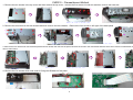
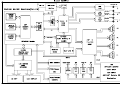
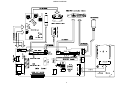
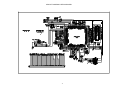
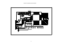
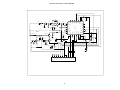
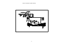
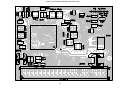
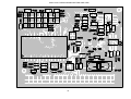
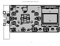
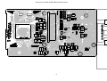
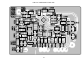
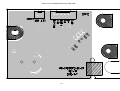
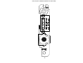
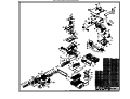
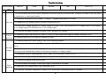
CMD310/ 55
Mini System
Service
Service
Service Manual
TABLE OF CONTENTS
DISMANTLING INSTRUCTIONS.................................................. 2
BLOCK DIAGRAM.........................................................................3
WIRING DIAGRAM........................................................................4
CIRCUIT DIAGRAM MAIN BOARD....................................................5-6
CIRCUIT DIAGRAM SERVO BOARD.................................................7
CIRCUIT DIAGRAM PANEL BOARD.......................................8
CIRCUIT DIAGRAM TUNER BOARD.......................................9
CIRCUIT DIAGRAM IPOD CONTACT BOARD........................10
CIRCUIT DIAGRAM POWER BOARD......................................11
Version1.0
314178537260
MAIN PCB COMPONENT LAYOUT..............................................12-13
SERVO PCB COMPONENT LAYOUT................................................14-15
PANEL PCB COMPONENT LAYOUT........................................... 16-17
TUNER PCB COMPONENT LAYOUT................................................18-19
IPOD CONTACT PCB COMPONENT LAYOUT.................................20-21
IPOD PCB COMPONENT LAYOUT....................................................22
POWER PCB COMPONENT LAYOUT...............................................23-24
USB.AUX PCB COMPONENT LAYOUT..............................................25-26
SET EXPLODER VIEW DRAWING ....................................................27
TROUBLE SHOOTING.........................................................................28-29
RECORDABLE
REWRITABLE
CMD310 -- Dismantlement Method
1. Remove the two screws in the top cover and then remove the top cover ; remove the five screws in heat sink and then remove the heat sink
Remove the screws in the top cover
Remove top cover
Remove the screws in the heat sink
Remove heat sink
2. Remove the six screws in the rear chassis and then remove the rear chassis ; Remove the four screws in left right of the base panel
Remove the six screws
Remove the screws on the left right side of the base panel
Remove the rear chassis
3. Remove the FFC which was connected the panel and main board, then remove the panel; Remove the screw in the main board and wire which was connect to small board, then
remove main board
Remove panel
Remove the screw and
wire
Remove main board
Main board
Remove FFC
4. Remove the five screws which was used for fixing the KB baord of the panel
Panel
Remove the five screws
2
PANEL PCB
3
WIRING DIAGRAM
4
CIRCUIT DIAGRAM -MAIN BOARD
5
6
CIRCUIT DIAGRAM -SERVO BOARD
7
CIRCUIT DIAGRAM -PANEL BOARD
SEG33
SEG28
27
SEG27
26
SEG26
25
SEG25
24
SEG24
23
SEG23
22
SEG22
21
SEG21
20
SEG20
19
SEG19
18
SEG18
17
SEG17
0.4
R902
R903
1
2
3
4
5
6
7
8
9
10
11
12
13
14
15
16
17
18
19
20
21
22
23
24
25
26
27
SEG01
SEG02
SEG03
SEG04
SEG05
SEG06
SEG07
SEG08
SEG09
SEG10
SEG11
SEG12
SEG13
SEG14
SEG15
SEG16
SEG17
SEG18
SEG19
SEG20
SEG21
SEG22
SEG23
SEG24
SEG25
SEG26
IC901
LCD-MC5502
0.68
330
SW902
SW903
M2/FOLDER
M3/RPT
CMD300-LCD
LCD901
SEG16
16
SEG16
SEG15
15
SEG15
SEG14
14
SEG14
SEG13
13
SEG13
SEG12
12
SEG12
SEG11
11
SEG11
SEG10
10
8
1
680P
SEG9
SEG17
SEG8
SI
SEG7
SEG18
SEG6
SCLK
SEG29
28
SEG55
SEG54
SEG53
SEG52
SEG49
SEG48
SEG47
SEG46
SEG45
SEG44
SEG43
SEG42
SEG41
SEG40
SEG39
SEG38
SEG37
SEG36
SEG35
SEG34
SEG33
SEG32
SEG31
SEG30
SEG29
SEG28
SEG27
28
29
30
31
32
33
34
35
36
37
38
39
40
41
42
43
44
45
46
47
48
49
50
51
52
53
54
SEG35
SEG36
SEG37
SEG38
SEG39
SEG40
SEG41
SEG42
SEG43
SEG44
SEG45
SEG46
SEG47
SEG34
33
SEG33
34
SEG34
35
36
SEG35
SEG36
37
SEG37
38
SEG38
39
SEG39
40
41
SEG40
SEG41
42
SEG42
43
SEG43
44
SEG44
45
46
SEG19
SEG1
CE
SEG30
29
6V8
10
SEG[00:99]
11
R912
R913
R914
R915
180
220
330
470
R904
12
470
0.99
R905
1.32
1.66
R906
R907
1K
1K5
680
2.0
R908
2.28
2K2
R909
2.53
R910
3K3
2.72
4K7
R911
2.88
8K2
13
14
GND2
GND2
SW913
SW915
SW914
DISP
BAND
SOUND
15
SW904
EQ/SOUND
SW905
MENU
SW906
SW908
16
17
R922
R923
47K
82K
M1
M2
M3
M4
MARK
1
MARK
1
MARK
1
MARK
1
EN901
POWER/MUTE
ENC
8
SW909
SOURCE
TUNE/SEEK-UP
TRACK-UP
5
GND
SEG20
9
2
KEY1
OSC
SEG31
30
ZD904
220
SW901
8
1
GND
KEY2
SEG21
SEG10
180
4
+5V
VSS
SEG32
31
7
3
FCE
REMO
ENVOL
SEG22
32
6
M1/SONG
FCLK
SEG23
VLC2
9
0.2
VLC1
SEG09
R901
SEG24
SEG08
FDATA
2P
INH
7
FINH
ZD903
6V8
GND2
0
LED5V
C904
2P
SEG25
SEG07
ZD902
6V8
VDD
6
4K7
5
C903
2P
SEG26
SEG06
GND1
4
C902
ZD901
6V8
COM3
C906
R927
R928
R929
2P
R931 47K
22
22
22
22
2
MIC
+
C901
2
SEG27
SEG01
BT-LED
1
3
61
R925 4K7
MIC-
GND2
64
R924
L-GND
60
63
R930
VOL-LED
MIC+
59
62
1
MIC901
ZD905
6V8
58
SEG28
COM2
SEG5
C910
10UF
473 C909
473 C908
104
C905
57
COM1
5
55
56
CON901
CON-17P
47
SEG48
SEG55
SEG45
48
GND1
SEG29
SEG05
GND1
SEG47
SEG48
54
SEG52/COM0
SEG4
53
SEG54
SEG30
SEG3
SEG53
10k
SEG31
SEG51
SEG2
52
SEG52
1
Q901
R952
SEG32
SEG50
4
1k
SEG49
3
51
2
50
GND2
R953
NC
SEG04
GND1
3
2
SEG03
9014
R951
SEG02
49
SEG49
GND1
SEG46
270
270
270
R947
LED916 BLUE
270
R946
270
R945
LED915 BLUE
LED914 BLUE
270
R944
270
R943
LED913 BLUE
LED912 BLUE
270
R942
LED911 BLUE
270
R940
270
R941
LED910 BLUE
LED909 BLUE
270
R939
270
R938
LED908 BLUE
LED907 BLUE
270
R937
LED906 BLUE
270
R935
R936
LED905 BLUE
270
R934
LED903 BLUE
LED904 BLUE
LED902 BLUE
LED901 BLUE
270
R932
R933
TP1TP2 TP3TP4TP5TP6
TUNER/SEEK-DN
TRACK-DN
SW910
SW911
SW912
M4/SHUF
M5/INTRO
M6/PAU
CIRCUIT DIAGRAM -TUNER BOARD
XT001
R014
100
32.768KHz
C008
220K
C018
Q004
4K7
9014S
16
14
VDD
13
VIO
15
GND
RCLK
ROUT
9
10
11
12
C016
FB152
C019
C025
1UF
C020
104
C011
103
L009
FB152
474
L007
220UH
C021
R010
1U
10
EC001
3
4
5
6
7
8
CN001
9
TUNER23
9
100
10
11
CLK
2
100
100
1
R012
R011
47UF
R013
12
DATA
104
RDS
C020
474
RES
10K
8
17
LOUT
L010
FB152
GND
R008
4K7
R009
AMI
18
DO
C112
+3V3
9018S
C015
104
RF-GND
L008
104
RFGND
10K
5
SI474X
DFS
103
L-OUT
Q002
CTUNE
R006
R007
R004
4
IC001
7
DGND
10M
AGC
104
R-OUT
C014 R005
122
3
C007
1MH
9014S
RFGND
333
RFGND
SCLK
C013
2
6
33UH
183
L005
Q102/Q003
FM ANT
FB152
L006
C017
19
SDIO
103
20
FMI
RST
C005
4K7
21
1
SEN
R002
AM
L004
2.7UH
22
DCLK
SK255
220NH
15P
47P
L003
23
INT
L002
24
GP01
47
30P
30P
C002
C006
R003
NC
220NH
Q001
NC
30P
C004
C003
NC
270K
L001
22P
22P
R001
C001
C009
CIRCUIT DIAGRAM -IPOD CONTACT BOARD
1
3
P5
2
P6
30P
IPOD701
4
USB_D+
5
USB_D-
C721
10P
C722
10P
P3
6
7
8
USB_PWR
9
C720
10P
EC710
10
11
P4
12
13
14
15
USB_GND
16
17
ipod-rx
18
ipod-tx
19
to bx8805
20
P2
21
22
23
24
26
P10
25
27
28
29
30
DET
31
32
33
34
10
CIRCUIT DIAGRAM -POWER BOARD
R711
Q703
9013
USBDC-ON
1K
CON701
FB
SD
100UF/25V
L712
47uH/2A
EC701
GND
GND
8
OUT
7
SK34(5819)
GND
6
EC705
GND
5
IN
2
100UF/25V
C710 C711
10P 104
R735
USBDC-ON
27P
10P
C713
C715
1K5/1%
R737
C714
104
EC702
R736
220uF/10V
7K5/1%
12K/1%
R738
47K
L709
FB
103
C712
Q702
9013
1
6
CON703
1
5
2
3
4
2
L704
2
1
L708
FB
4
FB
5
6
1
CON702
C723
10P
11
C724
10P
4
3
3
D-
D+
3
4
D+
D-
5
DET1
P20
6
WP
USB+5V
2
6
5
USBDC-ON1
6P/2.0
2P/2.5
IC701 AP1509
1
D1
2
0.47R/1W
3
1
4
100K
R712
BATT12V
C709
104
R734
DET
PCB LAYOUT-MAIN BOARD TOP SIDE VIEW
12
PCB LAYOUT-MAIN BOARD BOTTOM SIDE VIEW
13
PCB LAYOUT-SERVO BOARD TOP SIDE VIEW
14
PCB LAYOUT-SERVO BOARD BOTTOM SIDE VIEW
15
PCB LAYOUT-PANEL BOARD TOP SIDE VIEW
16
PCB LAYOUT-PANEL BOARD BOTTOM SIDE VIEW
17
PCB LYOUT-TUNER BOARD TOP SIDE VIEW
18
PCB LYOUT-TUNER BOARD BOTTOM SIDE VIEW
19
PCB LAYOUT-IPOD CONTACT BOARD TOP SIDE VIEW
20
PCB LAYOUT-IPOD CONTACT BOARD BOTTOM SIDE VIEW
21
PCB LAYOUT-IPOD BOARD TOP SIDE VIEW
22
PCB LAYOUT-POWER BOARD TOP SIDE VIEW
23
PCB LAYOUT-POWER BOARD BOTTOM SIDE VIEW
24
PCB LAYOUT-USB/AUX BOARD TOP SIDE VIEW
25
PCB LAYOUT-USB/AUX BOARD BOTTOM SIDE VIEW
26
SET EXPLODER VIEW DRAWING
Trouble shooting
Product Model
NO、
CMD310
Area
All area
failure
Tate
2012-1-12
failure cause
phenomena
a、 To check whether the ISO301(1,pin) connector of the tail of the unit is connect well , Whether it is loose of the 15A fuse of
the yellow wire, or insert non in place、
b、To check the connectors of the CON901
1
CON202
whether the socket of it is loose、
NO Power c、 To check the 5 pin voltage of the IC201(MCU) should be +5V0、
d、 To check each voltage regulator IC's output voltage is normal, IC303, 304 should be +9 V0 voltage output, IC302 should
+3 V3 voltage outputs, IC,05 should be +1 V2 voltage output、
e、 To check the oscillation frequence of crystal CF201 shuold be 32、7,8KHZ、
2
LCD
a、To check the Panel PCB on the LCD driver IC (IC901) of the 5, pin power supply is normal, should be +5 V0、
Display
abnormal b、To check whether the LCD Panel iron bracket for loose、
a、 To check whether the volume knob is turn to the minimum position、
b、 To check whether the unit is at MUTE mode, press SOURCE button and check whether it is effective of the input sound
source、
3
No audio
c、 To check whether the connection of 8 PIN audio output wire of ISO connector is correct; wrong connection or short circuit
output
to the ground will caused the protection of the power amplifier( no voltage output)、
d 、 To check the circuit of power amplifier IC501(7388 IC) and VOLUME IC402(7313 IC)、
e、 To check the voltage of 22 pin(MUTE) of power amplifier IC501(7388 IC) , normally should be +3V2、
a、 To check the antenna of the AM/FM tuner、
4
b、 To check whether the strength of then input signal of the tuner is too weak、
Radio
abnormal c、To check the 2 pin voltage of the IC401 should be +3 V3、
d、 To check the oscillation frequence of crystal XT001 of the tuner module,should be 32、7,8MHz、
28
remark
NO、
failure
phenomena
failure cause
a、 To check the iPHONE connector and the Dock socket whether there is poor contact、
b、 To check the SOURCE shoule be in iPHONE mode、
c、 To check whether it is normal when reading USB?
5
iPHONE
defective
d、 To check the 1 pin voltage of the CON801,should be +2V9、
e、 To check the SW2 switch in the Dock box、
f、 To check the CON301 and CON801 connector on the main board , whether the plugs of it is loose、
g、To check the 1 pin voltage of the CON703 in the dock, should be +5V0、
h、To check in the dock the CON701
CON702
CON703 connector ,whether the plugs of it is loose、
a、 To check whether the USB signal format is correspond to the request of the unit、
6
USB defective
b、 To check the voltage of the USB connector of the top first pin , should be +5V、
c、 To check whether there is any wearing and scratch of the shrapnel and pin of the panel USB、
d、To check the CON703 connectors on the main board , whether the plugs of it is loose、
a、 To check the SOURCE shoule be in MP3-LINK mode、
7
AUX defective b、 To check the AUX IN input signal、
c、 To check the CON402 connectors on the main board,whether the plugs of it is loose、
a、To check the unit should be in pair with the BT phone connection status、
8
BT defective b、To check the 4 pin voltage of BT module,should be +5V0、
c、To check the 17PIN FFC flat cable in the panel to the main board, whether the plugs of it is loose、
9
Dock door
defective
a、Press the EJECT button, to do a pull and push the dock operation、
29
remark