1
High Performance AC Drive
Phase II Control
Firmware Versions
1.xx - 4.001
User Manual
Important User Information
Solid state equipment has operational characteristics differing from those of
electromechanical equipment. Safety Guidelines for the Application,
Installation and Maintenance of Solid State Controls (Publication SGI-1.1
available from your local Rockwell Automation sales office or online at http://
www.rockwellautomation.com/literature) describes some important differences
between solid state equipment and hard-wired electromechanical devices.
Because of this difference, and also because of the wide variety of uses for solid
state equipment, all persons responsible for applying this equipment must
satisfy themselves that each intended application of this equipment is
acceptable.
In no event will Rockwell Automation, Inc. be responsible or liable for indirect
or consequential damages resulting from the use or application of this
equipment.
The examples and diagrams in this manual are included solely for illustrative
purposes. Because of the many variables and requirements associated with any
particular installation, Rockwell Automation, Inc. cannot assume responsibility
or liability for actual use based on the examples and diagrams.
No patent liability is assumed by Rockwell Automation, Inc. with respect to use
of information, circuits, equipment, or software described in this manual.
Reproduction of the contents of this manual, in whole or in part, without
written permission of Rockwell Automation, Inc. is prohibited.
Throughout this manual, when necessary we use notes to make you aware of
safety considerations.
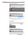
!
WARNING: Identifies information about practices or
circumstances that can cause an explosion in a hazardous
environment, which may lead to personal injury or death, property
damage, or economic loss.
Important: Identifies information that is critical for successful application and
understanding of the product.
!
ATTENTION: Identifies information about practices or
circumstances that can lead to personal injury or death, property
damage, or economic loss. Attentions help you:
• identify a hazard
• avoid the hazard
• recognize the consequences
Shock Hazard labels may be located on or inside the equipment
(e.g., drive or motor) to alert people that dangerous voltage may be
present.
Burn Hazard labels may be located on or inside the equipment
(e.g., drive or motor) to alert people that surfaces may be at
dangerous temperatures.
PowerFlex is a registered trademark of Rockwell Automation, Inc.
DriveExplorer, DriveExecutive, and SCANport are trademarks of Rockwell Automation, Inc.
PLC is a registered trademark of Rockwell Automation, Inc.
Summary of Changes
Manual Updates
This information summarizes the changes to the PowerFlex 700S High
Performance AC Drive - Phase II Control User Manual, publication
20D-UM006, since the August 2006 release.
Change
See Page...
Updated the “Important” information regarding the use of an Auxiliary Power Supply with Voltage
Feedback boards on drives manufactured before June 2006.
The following new parameters were added for firmware versions 4.001:
3-1-3-114
459
460
461
462
544
586
587
588
589
590
591
[IdsCompCoeff Mot]
[IdsCompCoeff Reg]
[SlipReg Off Iqs]
[VqsReg Off Freq]
[External DB Res]
[IdsCmd Slew Rate]
[SlipReg Err Lmt]
[VqsReg Err Lmt]
[Err Count Lmt]
[RsTempCoefAdjust]
[RsTmpCoefAdjstEn]
592 [VqsReg On Hystr]
593 [SlipReg On Hystr]
1124 [Home Actual Pos]
1155 [Heidn VM Pos Ref]
1156 [Heidn VM Enc PPR]
1160 [VirtEncPositFast]
1161 [EGR Config]
1162 [EGR Mul]
1163 [EGR Div]
1164 [EGR Pos Input]
1165 [EGR Pos Output]
1166 [EGR Pos Preset]
1170 [MC Generic 1]
1171 [MC Generic 2]
1172 [MC Generic 3]
1173 [MC Generic 4]
1174 [MC Generic 5]
1175 [MC Generic 6]
1176 [MC Generic 7]
1177 [MC Generic 8]
1178 [MC Generic 9]
1179 [MC Generic 10]
The following parameters were updated for firmware version 4.001:
153
156
161
263
264
266
267
277
314
357
360
457
466
510
[Control Options]
[Start Inhibits]
[Logic TP Sel]
[Heidenhain0 Cnfg]
[Heidenhain0 Stat]
[Heidn Encdr Type]
[Heidn Encdr PPR]
[Reslvr0 Type Sel]
[VPL Firmware Rev]
[Curr Ref TP Sel]
[Min Flux]
[MC Firmware Rev]
[MC TP1 Select]
[FVC Mode Config]
512
515
533
553
701
788
789
790
791
792
793
794
795
825
[PMag Mode Config]
[FVC Tune Config]
[SlewRateTimeLimt]
[Slip Slew Rate]
[FdbkAxis FdbkSel]
[Xsync In 1]
[Xsync Out 1]
[Xsync In 2]
[Xsync Out 2]
[Xsync Out 2 Dly]
[Xsync In 3]
[Xsync Out 3]
[Xsync Out 3 Dly]
[Dig In1 Sel]
3-1-3-114
826 [Dig In2 Sel]
827 [Dig In3 Sel]
828 [Dig In4 Sel]
829 [Dig In5 Sel]
830 [Dig In6 Sel]
1000 [UserFunct Enable]
1122 [Home Speed]
1123 [Home Position]
1136 [PPMP Rev Spd Lim]
1137 [PPMP Fwd Spd Lim]
1138 [PPMP Over Ride]
1145 [PPMP TP Select]
Added the “Electronic Gear Ratio” Group to the User Function file.
Added required encoder PPR rating values
Updated the “Inputs & Outputs - Digital” block diagram to reflect new values
Added the new “Virtual Master Encoder” block diagram
Updated the “User Functions 2” block diagram
Updated parameter names in the “Inverter Overload IT” block diagram
Added an “Application Note” regarding Motor Overload Memory Retention
3-14
A-4
B-11
B-19
B-21
B-25
C-6
This information summarizes the changes to the PowerFlex 700S High
Performance AC Drive - Phase II Control User Manual, publication
20D-UM006, since the March 2006 release.
Change
See Page...
Updated the Catalog Number Explanation
Added a note for Frame 6 power terminals connections
Added a note to indicate that the Analog Inputs are not isolated
Added maximum value calculation for Par 81 [Spd Reg P Gain]
Added note referencing “Cable Tuning Tests” to Par 268 [Resolver0 Cnfg]
Preface-5
1-12
1-22
3-19
3-42
soc-2
Change
See Page...
Added bit 14 to Pars 322 [Exception Event3], 325 [Fault Status 3], and 328 [Alarm Status 3]
3-48, 3-49,
3-49
3-70
3-94
3-97
3-98
3-106
4-11
A-1
A-6
A-7
B-28
F-4, H-4
K-1
Added a note for value 1 “FOC 2” for Par 485 [Motor Ctrl Mode]
Updated Par 796 [Posit Gear Ratio] to be linkable
Updated the description for options 34 “UserGen Sel0” - 37 “UserGen Sel3” for Pars 825 - 830
Added a list of parameters corresponding to the value selected in Par 831 [Anlg Out1 Sel]
Updated the description for Par 1022 [Sel Switch Ctrl]
Added new fault code 79 “HiHP Bus Data”
Updated the Bus Overvoltage Trip levels
Added information on DPI device limitations
Update the “Drive, Fuse & Circuit Breaker Ratings” tables
Updated the DriveLogix - Motion Control Block Diagram
Updated wiring diagram for Rotary Encoder connections
Added new Appendix for SynchLink Specifications
This information summarizes the changes to the PowerFlex 700S High
Performance AC Drive - Phase II Control User Manual, publication
20D-UM006, since the September 2005 release.
Change
See Page...
Updated the Power Terminal Block Specification Descriptions
Updated the Terminal Block specifications for digital input leakage current
Updated the HIM Start Up Menu diagram
Updated the Min./Max. values for parameter 75 [Rev Speed Limit]
Updated the Min./Max. values for parameter 76 [Fwd Speed Limit]
Added values 9 and 10 to parameter 150 [Logic State Mach]
Added value 8 to parameter 165 [Tune Test Status]
Updated the trigger Source settings for parameter 236 [RegisLtch 0/1Cnfg]
Changed parameter 321 [Exception Event2] / bit 14 to a non-configurable alarm
Changed parameter 322 [Exception Event3] / bit 11, 12, 13, 21 and 28 to a non-configurable
alarms
Changed parameter 324 [Fault Status 2] / bit 14 to a non-configurable alarm
Changed parameter 325 [Fault Status 3] / bit 21 to Drive Homing” and bit 28 to “+/- 12v Pwr”
Changed parameter 327 [Alarm Status 2] / bit 14 to a non-configurable alarm
Changed parameter 328 [Alarm Status 3] / bit 21 to Drive Homing” and bit 28 to “+/- 12v Pwr”
Added values 45, 46 and 47 to parameter 347 [Drive OL TP Sel]
Added values 20 - 52 to parameter 357 [Curr Ref TP Sel]
Changed bit 3 to “FastFluxDsbl” for parameter 510 [FVC Mode Config]
Changed bit 3 to “FastFluxDsbl” for parameter 513 [V/Hz Mode Config]
Updated the default and Min./Max. values for parameter 532 [Maximum Frequency]
Change bit 18 to ”Vqs Reg Act” for parameter 555 [MC Status]
Added bit 9 “Watch Fb Arm” and bit 10 ”WatchFbPosit” to parameter 691 [Motn EventStatus]
Added bit 7 “Watch Fb Rev” to parameter 692 [Motn Event Ctrl]
Updated Parameter 554 [LED Status] to include a description
Updated the description for bit 7 “AbsoluteMode” of parameter 740 [Position Control]
Updated the description for bit 0 “Absolute” of parameter 1134 [PPMP Control]
Updated fault 33 “+/- 15volt Power” to new voltage band settings
Added new event 86 “Drive Homing”
Added new event 93 “+/- 12volt Power Alarm”
Updated the Specifications table for C-tick Agency Certification, drive sound levels, and encoder
voltage supply data.
Updated the Drive, Fuse & Circuit Breaker Ratings tables.
Updated wiring diagram for Rotary Encoder connections.
Added new Appendix for ATEX approved PowerFlex 700S Phase II Drives in Group II Category (2)
applications with ATEX approved motors.
1-12
1-23
2-7
3-18
3-18
3-24
3-29
3-35
3-48
3-48
3-48
3-49
3-49
3-49
3-53
3-54
3-72
3-73
3-76
3-78
3-84
3-84
3-77
3-89
3-113
4-8
4-11
4-11
A-1
A-7
H-4
J-1
soc-3
This information summarizes the changes to the PowerFlex 700S High
Performance AC Drive - Phase II Control User Manual, publication
20D-UM006, since the August 2005 release.
Change
See Page...
The following new parameters were added for firmware versions 3.01:
3-1-3-114
49
50
54
119
120
341
368
533
551
552
553
554
669
712
713
714
717
718
719
720
721
722
723
724
725
726
727
728
729
730
731
[Selected SpdRefA]
[Selected SpdRefB]
[Inertia TrqLpfBW]
[SLAT ErrorSetpnt]
[SLAT Dwell Time]
[Mtr I2T Count]
[Cnv NotLogin Cfg]
[SlewRateTimeLimt]
[CurrFdbk AdjTime]
[Slip Preload Val]
[Slip Slew Rate]
[LED Status]
[Write Mask]
[Write Mask Act]
[Logic Mask Act]
[Port Mask Act]
[PLL TP Select]
[PLL TP DataDInt]
[PLL TP DataReal]
[PLL Control]
[PLL Position Ref]
[PLL BandWidth]
[PLL Rev Input]
[PLL Rev Output]
[PLL EPR Input]
[PLL EPR Output]
[PLL VirtEncdrRPM]
[PLL Ext Spd Ref]
[PLL Ext SpdScale]
[PLL LPFilter BW]
[PLL Posit Out]
732 [PLL Posit OutAdv]
733 [PLL FiltPositOut]
734 [PLL Speed Out]
735 [PLL SpeedOut Adv]
848 [Dig Out1 On Time]
849 [Dig Out1 OffTime]
853 [Dig Out2 On Time]
854 [Dig Out2 OffTime]
858 [Rly Out3 On Time]
859 [Rly Out3 OffTime]
1093 [Anlg In1LossCnfg]
1094 [Anlg In2LossCnfg]
1095 [Anlg In3LossCnfg]
1096 [AddSub 1 Input]
1097 [AddSub 1 Add]
1098 [AddSub 1 Subtrct]
1099 [AddSub 1 Result]
1100 [AddSub 2 Input]
1101 [AddSub 2 Add]
1102 [AddSub 2 Subtrct]
1103 [AddSub 2 Result]
1104 [AddSub 3 Input]
1105 [AddSub 3 Add]
1106 [AddSub 3 Subtrct]
1107 [AddSub 3 Result]
1108 [DelTmr1 TrigData]
1109 [DelTmr1 Trig Bit]
1110 [DelayTimer1PrSet]
1111 [DelayTimer1Accum]
1112 [DelayTimer1Stats]
1113 [DelTmr2 TrigData]
1114 [DelTmr2 Trig Bit]
1115 [DelayTimer2PrSet]
1116 [DelayTimer2Accum]
1117 [DelayTimer2Stats]
1120 [Home Accel Time]
1121 [Home Decel Time]
1122 [Home Speed]
1123 [Home Position]
1125 [DC Brake Level]
1126 [DC Brake Time]
1130 [PPMP Pos Command]
1131 [PPMP Pos Mul]
1132 [PPMP Pos Div]
1133 [PPMP Scaled Cmd]
1134 [PPMP Control]
1135 [PPMP Status]
1136 [PPMP Rev Spd Lim]
1137 [PPMP Fwd Spd Lim]
1138 [PPMP Over Ride]
1139 [PPMP Accel Time]
1140 [PPMP Decel Time]
1141 [PPMP SCurve Time]
1142 [PPMP Spd Output]
1143 [PPMP Pos Output]
1144 [PPMP Pos To Go]
1145 [PPMP TP Select]
1146 [PPMP TP DataDInt]
1147 [PPMP TP DataReal]
1150 [DInt2Real2 In]
1151 [DInt2Real2 Scale]
1152 [DInt2Real2Result]
soc-4
Change
See Page...
The following parameters were updated for firmware version 3.01:
3-1-3-114
81
84
92
110
132
147
149
150
153
157
165
222
223
224
259
263
264
266
306
322
325
328
[Spd Reg P Gain]
[SpdReg AntiBckup]
[SpdReg P Gain Mx]
[Speed/TorqueMode]
[Inert Adapt Sel]
[FW Functions En]
[FW FunctionsActl]
[Logic State Mach]
[Control Options]
[Logic Ctrl State]
[Tune Test Status]
[Mtr Fdbk Sel Pri]
[Mtr Fdbk Sel Alt]
[TachSwitch Level]
[Stegmann0 Cnfg]
[Heidenhain0 Cnfg]
[Heidenhain0 Stat]
[Heidn Encdr Type]
[DC Bus Voltage]
[Exception Event3]
[Fault Status 3]
[Alarm Status 3]
370 [HiHp InPhsLs Cfg]
412 [Power EE TP Sel]
414 [Brake/Bus Cnfg]
416 [Brake PulseWatts]
417 [Brake Watts]
420 [Pwr Strct Mode]
465 [MC Diag Error 3]
466 [MC TP1 Select]
475 [MC FaultTPSelect]
486 [Rated Slip Freq]
490 [StatorInductance]
510 [FVC Mode Config]
511 [FVC2 Mode Config]
512 [PMag Mode Config]
514 [Test Mode Config]
549 [Vuv Fdbk Offset]
550 [Vvw Fdbk Offset]
740 [Position Control]
741 [Position Status]
742 [Position Ref Sel]
777 [PositionFdbk Sel]
796 [Posit Gear Ratio]
825 [Dig In1 Sel]
826 [Dig In2 Sel]
827 [Dig In3 Sel]
828 [Dig In4 Sel]
829 [Dig In5 Sel]
830 [Dig In6 Sel]
904 [SL Node Cnfg]
905 [SL Rx CommFormat]
906 [SL Rx DirectSel0]
907 [SL Rx DirectSel1]
908 [SL Rx DirectSel2]
909 [SL Rx DirectSel3]
910 [SL Tx Comm Format]
911 [SL Tx DirectSel0]
912 [SL Tx DirectSel1]
913 [SL Tx DirectSel2]
914 [SL Tx DirectSel3]
1000 [UserFunct Enable]
1047 [DInt2Real1 In]
1048 [DInt2Real1 Scale]
1049 [DInt2Real1Result]
The following new fault codes were added for firmware version 3.01:
76
77
HiHP HardwareVer
HiHP CurrUnblnce
78
94
HiHP VoltUnblnce
Analog In 1 Loss
Encoder specifications updated
Updated and new Control Block Diagrams
95
96
4-5
Analog In 2 Loss
Analog In 3 Loss
A-1 & A-7
B-1
soc-5
This information summarizes the changes to the PowerFlex 700S High
Performance AC Drive - Phase II Control User Manual, publication
20D-UM006 since the August 2004 release.
Change
See Page...
URL for Rockwell Automation Technical Support added
Catalog Number Explanation updated
DIP Switch Settings table updated
The following new parameters were added for firmware versions 2.03 and 2.04:
Preface-2
Preface-5
1-29
3-1-3-114
•
•
•
•
•
•
•
•
•
•
•
•
•
•
•
•
42
98
99
107
136
137
138
139
170
263
264
265
266
267
285
296
[Jerk]
[Slip RPM @ FLA]
[Slip Comp Gain]
[Slip RPM Meter]
[Skip Speed 1]
[Skip Speed 2]
[Skip Speed 3]
[Skip Speed Band]
[Flying StartGain]
[Heidenhain0 Cnfg]
[Heidenhain0 Stat]
[Heidn Mkr Offset]
[Heidn Encdr Type]
[Heidn Encdr PPR]
[Linear1 Config]
[Motor Freq Ref]
332
333
334
362
363
364
471
473
474
475
476
478
479
480
481
482
[700L EventStatus]
[700L FaultStatus]
[700L AlarmStatus]
[Current Limit Gain]
[Ki Current Limit]
[Kd Current Limit]
[Estimated Torque]
[MC TP2 Select]
[MC TP2 Value]
[MC FaultTPSelect]
[MC FaultTP Value]
[VPL Mem Password]
[VPL Mem Address]
[VPL Mem Data Int]
[VPL Mem Data Flt]
[VVPL Mem Data Bit]
483
484
513
527
528
529
530
531
532
541
542
545
546
547
548
[VPL Mem Link Int]
[VPL Mem Link Flt]
[V/Hz Mode Config]
[Start/Acc Boost]
[Run Boost]
[Break Voltage]
[Break Frequency]
[Maximum Voltage]
[Maximum Freq]
[SrLss Angl Comp]
[SrLss Volt Comp]
[Bus Reg Ki]
[Bus Reg Kp]
[Bus Reg Kd]
[Bus Reg ACR Kp]
The following parameters were updated for firmware versions 2.03 and 2.04:
•
•
•
•
•
•
•
•
153
245
266
268
272
316
322
328
[Control Options]
[Spd Fdbk TP Sel]
[Heidn Encdr Type]
[Resolver0 Cnfg]
[Reslvr0 SpdRatio]
[SynchLink Status]
[Exception Event3]
[Alarm Status 3]
347
466
787
825
826
827
828
829
[Drive OL TP Sel]
[MC TP1 Select]
[Xsync Gen Period]
[Dig In1 Sel]
[Dig In2 Sel]
[Dig In3 Sel]
[Dig In4 Sel]
[Dig In5 Sel]
830 [Dig In6 Sel]
905 [SL Rx CommFormat]
906 [SL Rx DirectSel0]
907 [SL Rx DirectSel1]
908 [SL Rx DirectSel2]
909 [SL Rx DirectSel2]
1000 [UserFunct Enable]
Added new fault codes and descriptions/actions
Specifications Table and Recommended Protection Devices tables updated
Updated and New Control Block Diagrams
Updated “HIM Overview” to include HIM menu chart and steps for viewing, editing and linking
parameters using the HIM.
Added new Appendix I - PowerFlex 700S Permanent Magnet Motor Specifications
4-5
A-1 & A-7
B-1
D-1
I-1
soc-6
Table of Contents
Important User Information . . . . . . . . . . . . . . . . . . . . . . . . . . . . . . . . . . . . . . . . . . . . . . . 1-2
Summary of
Changes
Manual Updates . . . . . . . . . . . . . . . . . . . . . . . . . . . . . . . . . . . . . . . . . . . . . . . . . . . . . . . . . i-1
Preface
Overview
Who Should Use This Manual . . . . . . . . . . . . . . . . . . . . . . . . . . . . . . . . . . . . . . . . . . . . .
What Is Not In This Manual . . . . . . . . . . . . . . . . . . . . . . . . . . . . . . . . . . . . . . . . . . . . . . .
Recommended Documentation . . . . . . . . . . . . . . . . . . . . . . . . . . . . . . . . . . . . . . . . . . . . .
Manual Conventions . . . . . . . . . . . . . . . . . . . . . . . . . . . . . . . . . . . . . . . . . . . . . . . . . . . . .
Drive Frame Sizes . . . . . . . . . . . . . . . . . . . . . . . . . . . . . . . . . . . . . . . . . . . . . . . . . . . . . . .
General Precautions . . . . . . . . . . . . . . . . . . . . . . . . . . . . . . . . . . . . . . . . . . . . . . . . . . . . .
Class 1 LED Product . . . . . . . . . . . . . . . . . . . . . . . . . . . . . . . . . . . . . . . . . . . . . . . . . . .
Catalog Number Explanation . . . . . . . . . . . . . . . . . . . . . . . . . . . . . . . . . . . . . . . . . . . . . .
Catalog Number Explanation, Cont’d . . . . . . . . . . . . . . . . . . . . . . . . . . . . . . . . . . . . . . . .
Chapter 1
P-1
P-1
P-1
P-3
P-3
P-4
P-4
P-5
P-6
Installation/Wiring
Chapter Objectives . . . . . . . . . . . . . . . . . . . . . . . . . . . . . . . . . . . . . . . . . . . . . . . . . . . . . . 1-1
Opening the Cover . . . . . . . . . . . . . . . . . . . . . . . . . . . . . . . . . . . . . . . . . . . . . . . . . . . . . . 1-2
Mounting Clearances . . . . . . . . . . . . . . . . . . . . . . . . . . . . . . . . . . . . . . . . . . . . . . . . . . . . 1-3
Operating Temperatures . . . . . . . . . . . . . . . . . . . . . . . . . . . . . . . . . . . . . . . . . . . . . . . . 1-3
AC Supply Source Considerations . . . . . . . . . . . . . . . . . . . . . . . . . . . . . . . . . . . . . . . . . . 1-4
Unbalanced, Ungrounded or Resistive Grounded Distribution Systems . . . . . . . . . . . 1-4
Input Power Conditioning . . . . . . . . . . . . . . . . . . . . . . . . . . . . . . . . . . . . . . . . . . . . . . . 1-5
Grounding Requirements . . . . . . . . . . . . . . . . . . . . . . . . . . . . . . . . . . . . . . . . . . . . . . . . . 1-5
Recommended Grounding Scheme. . . . . . . . . . . . . . . . . . . . . . . . . . . . . . . . . . . . . . . . 1-5
Shield Termination - SHLD . . . . . . . . . . . . . . . . . . . . . . . . . . . . . . . . . . . . . . . . . . . . . 1-6
RFI Filter Grounding. . . . . . . . . . . . . . . . . . . . . . . . . . . . . . . . . . . . . . . . . . . . . . . . . . . 1-6
Fuses and Circuit Breakers . . . . . . . . . . . . . . . . . . . . . . . . . . . . . . . . . . . . . . . . . . . . . . . . 1-6
Power Wiring. . . . . . . . . . . . . . . . . . . . . . . . . . . . . . . . . . . . . . . . . . . . . . . . . . . . . . . . . . . 1-7
Power Cable Types Acceptable for 200-600 Volt Installations. . . . . . . . . . . . . . . . . . . 1-7
Motor Cable Lengths. . . . . . . . . . . . . . . . . . . . . . . . . . . . . . . . . . . . . . . . . . . . . . . . . . . 1-9
Power Terminal Blocks . . . . . . . . . . . . . . . . . . . . . . . . . . . . . . . . . . . . . . . . . . . . . . . . . 1-9
Cable Entry Plate Removal . . . . . . . . . . . . . . . . . . . . . . . . . . . . . . . . . . . . . . . . . . . . . . 1-9
Power Wiring Access Panel Removal . . . . . . . . . . . . . . . . . . . . . . . . . . . . . . . . . . . . . 1-10
AC Input Phase Selection (Frames 5 & 6 Only) . . . . . . . . . . . . . . . . . . . . . . . . . . . . . 1-10
Cooling Fan Voltage . . . . . . . . . . . . . . . . . . . . . . . . . . . . . . . . . . . . . . . . . . . . . . . . . . 1-10
Selecting/Verifying Fan Voltage (Frames 5 & 6 Only) . . . . . . . . . . . . . . . . . . . . . . . . 1-10
Important Common Bus (DC Input) Application Notes . . . . . . . . . . . . . . . . . . . . . . . 1-12
Dynamic Brake Resistor Considerations. . . . . . . . . . . . . . . . . . . . . . . . . . . . . . . . . . . 1-15
Using Input/Output Contactors . . . . . . . . . . . . . . . . . . . . . . . . . . . . . . . . . . . . . . . . . . . . 1-16
Using PowerFlex® 700S Drives with Regenerative Power Units. . . . . . . . . . . . . . . . . . 1-16
Regenerative Unit to Drive Connections. . . . . . . . . . . . . . . . . . . . . . . . . . . . . . . . . . . 1-16
Disconnecting MOVs and Common Mode Capacitors. . . . . . . . . . . . . . . . . . . . . . . . . . 1-17
I/O Wiring . . . . . . . . . . . . . . . . . . . . . . . . . . . . . . . . . . . . . . . . . . . . . . . . . . . . . . . . . . . . 1-19
ATEX Approved Drives and Motors . . . . . . . . . . . . . . . . . . . . . . . . . . . . . . . . . . . . . . 1-20
Wiring the Main Control Board I/O Terminals . . . . . . . . . . . . . . . . . . . . . . . . . . . . . . 1-20
Auxiliary Power Supply (High Power Only) . . . . . . . . . . . . . . . . . . . . . . . . . . . . . . . 1-21
Hardware Enable Circuitry . . . . . . . . . . . . . . . . . . . . . . . . . . . . . . . . . . . . . . . . . . . . . 1-22
Main Control Board I/O Configuration Settings. . . . . . . . . . . . . . . . . . . . . . . . . . . . . 1-28
2
Table of Contents
CE Conformity. . . . . . . . . . . . . . . . . . . . . . . . . . . . . . . . . . . . . . . . . . . . . . . . . . . . . . . . .
Low Voltage Directive (73/23/EEC) . . . . . . . . . . . . . . . . . . . . . . . . . . . . . . . . . . . . . .
EMC Directive (89/336/EEC) . . . . . . . . . . . . . . . . . . . . . . . . . . . . . . . . . . . . . . . . . . .
General Notes . . . . . . . . . . . . . . . . . . . . . . . . . . . . . . . . . . . . . . . . . . . . . . . . . . . . . . .
Essential Requirements for CE Compliance . . . . . . . . . . . . . . . . . . . . . . . . . . . . . . . .
Chapter 2
Start-Up
Prepare for Drive Start-Up. . . . . . . . . . . . . . . . . . . . . . . . . . . . . . . . . . . . . . . . . . . . . . . . .
Before Applying Power to the Drive . . . . . . . . . . . . . . . . . . . . . . . . . . . . . . . . . . . . . . .
Applying Power to the Drive . . . . . . . . . . . . . . . . . . . . . . . . . . . . . . . . . . . . . . . . . . . . .
Assisted Start-Up . . . . . . . . . . . . . . . . . . . . . . . . . . . . . . . . . . . . . . . . . . . . . . . . . . . . . . . .
Chapter 3
1-29
1-29
1-30
1-30
1-30
2-1
2-1
2-3
2-5
Programming and Parameters
About Parameters. . . . . . . . . . . . . . . . . . . . . . . . . . . . . . . . . . . . . . . . . . . . . . . . . . . . . . . . 3-1
How Parameters are Organized . . . . . . . . . . . . . . . . . . . . . . . . . . . . . . . . . . . . . . . . . . . . . 3-3
Parameter Data in Linear List Format . . . . . . . . . . . . . . . . . . . . . . . . . . . . . . . . . . . . . . . 3-15
Parameter Cross Reference By Name . . . . . . . . . . . . . . . . . . . . . . . . . . . . . . . . . . . . . . 3-117
Chapter 4
Troubleshooting
Chapter Objectives. . . . . . . . . . . . . . . . . . . . . . . . . . . . . . . . . . . . . . . . . . . . . . . . . . . . . . .
Drive Status . . . . . . . . . . . . . . . . . . . . . . . . . . . . . . . . . . . . . . . . . . . . . . . . . . . . . . . . . . . .
LED Indications. . . . . . . . . . . . . . . . . . . . . . . . . . . . . . . . . . . . . . . . . . . . . . . . . . . . . . .
Precharge Board LED Indications . . . . . . . . . . . . . . . . . . . . . . . . . . . . . . . . . . . . . . . . .
HIM Indication . . . . . . . . . . . . . . . . . . . . . . . . . . . . . . . . . . . . . . . . . . . . . . . . . . . . . . .
Manually Clearing Faults. . . . . . . . . . . . . . . . . . . . . . . . . . . . . . . . . . . . . . . . . . . . . . . . . .
Faults and Alarms . . . . . . . . . . . . . . . . . . . . . . . . . . . . . . . . . . . . . . . . . . . . . . . . . . . . . . .
Fault/Alarm Descriptions. . . . . . . . . . . . . . . . . . . . . . . . . . . . . . . . . . . . . . . . . . . . . . . . . .
Appendix A
4-1
4-1
4-2
4-3
4-4
4-4
4-4
4-5
Supplemental Information
Chapter Objectives. . . . . . . . . . . . . . . . . . . . . . . . . . . . . . . . . . . . . . . . . . . . . . . . . . . . . . .
Specifications . . . . . . . . . . . . . . . . . . . . . . . . . . . . . . . . . . . . . . . . . . . . . . . . . . . . . . . . . .
DPI Communication Configurations . . . . . . . . . . . . . . . . . . . . . . . . . . . . . . . . . . . . . . . . .
Typical Programmable Controller Configurations. . . . . . . . . . . . . . . . . . . . . . . . . . . . .
Logic Command Word. . . . . . . . . . . . . . . . . . . . . . . . . . . . . . . . . . . . . . . . . . . . . . . . . .
Logic Status Word . . . . . . . . . . . . . . . . . . . . . . . . . . . . . . . . . . . . . . . . . . . . . . . . . . . . .
DPI Device Limitations . . . . . . . . . . . . . . . . . . . . . . . . . . . . . . . . . . . . . . . . . . . . . . . . .
Output Devices . . . . . . . . . . . . . . . . . . . . . . . . . . . . . . . . . . . . . . . . . . . . . . . . . . . . . . . . .
Drive, Fuse & Circuit Breaker Ratings . . . . . . . . . . . . . . . . . . . . . . . . . . . . . . . . . . . . . . .
Fuse Size . . . . . . . . . . . . . . . . . . . . . . . . . . . . . . . . . . . . . . . . . . . . . . . . . . . . . . . . . . . .
Fuse Type . . . . . . . . . . . . . . . . . . . . . . . . . . . . . . . . . . . . . . . . . . . . . . . . . . . . . . . . . . . .
A-1
A-1
A-5
A-5
A-5
A-6
A-6
A-7
A-7
A-7
A-7
Table of Contents
List of Motors with Compatible Thermistor Ratings . . . . . . . . . . . . . . . . . . . . . . . . . . .
Auxiliary Power Supply . . . . . . . . . . . . . . . . . . . . . . . . . . . . . . . . . . . . . . . . . . . . . . . . .
Drive Frame Size to HP/kW Ratings Cross Reference . . . . . . . . . . . . . . . . . . . . . . . . . .
Approximate Dimensions . . . . . . . . . . . . . . . . . . . . . . . . . . . . . . . . . . . . . . . . . . . . . . . .
Appendix B
3
A-30
A-31
A-31
A-33
Control Block Diagrams
List of Control Block Diagrams . . . . . . . . . . . . . . . . . . . . . . . . . . . . . . . . . . . . . . . . . . . . B-1
Diagram Conventions and Definitions . . . . . . . . . . . . . . . . . . . . . . . . . . . . . . . . . . . . . . . B-2
Appendix C
Application Notes
Input Voltage Range/Tolerance . . . . . . . . . . . . . . . . . . . . . . . . . . . . . . . . . . . . . . . . . . . . .
Motor Control Mode . . . . . . . . . . . . . . . . . . . . . . . . . . . . . . . . . . . . . . . . . . . . . . . . . . . . .
Field Oriented Control . . . . . . . . . . . . . . . . . . . . . . . . . . . . . . . . . . . . . . . . . . . . . . . . .
Permanent Magnet Control . . . . . . . . . . . . . . . . . . . . . . . . . . . . . . . . . . . . . . . . . . . . . .
Volts/Hertz Control - v2.003 and later . . . . . . . . . . . . . . . . . . . . . . . . . . . . . . . . . . . . .
Motor Overload . . . . . . . . . . . . . . . . . . . . . . . . . . . . . . . . . . . . . . . . . . . . . . . . . . . . . . . . .
Setting Parameter 338 [Mtr I2T Spd Min] . . . . . . . . . . . . . . . . . . . . . . . . . . . . . . . . . .
Motor Overload Memory Retention Per 2005 NEC . . . . . . . . . . . . . . . . . . . . . . . . . . .
Stop Dwell Time . . . . . . . . . . . . . . . . . . . . . . . . . . . . . . . . . . . . . . . . . . . . . . . . . . . . . . . .
Setpt 1 Data . . . . . . . . . . . . . . . . . . . . . . . . . . . . . . . . . . . . . . . . . . . . . . . . . . . . . . . . . . . .
Setpt 2 Data . . . . . . . . . . . . . . . . . . . . . . . . . . . . . . . . . . . . . . . . . . . . . . . . . . . . . . . . . . . .
Appendix D
HIM Overview
External and Internal Connections . . . . . . . . . . . . . . . . . . . . . . . . . . . . . . . . . . . . . . . . . .
LCD Display Elements . . . . . . . . . . . . . . . . . . . . . . . . . . . . . . . . . . . . . . . . . . . . . . . . . . .
ALT Functions. . . . . . . . . . . . . . . . . . . . . . . . . . . . . . . . . . . . . . . . . . . . . . . . . . . . . . . . . .
Menu Structure . . . . . . . . . . . . . . . . . . . . . . . . . . . . . . . . . . . . . . . . . . . . . . . . . . . . . . . . .
Viewing and Editing Parameters . . . . . . . . . . . . . . . . . . . . . . . . . . . . . . . . . . . . . . . . . . . .
LCD HIM . . . . . . . . . . . . . . . . . . . . . . . . . . . . . . . . . . . . . . . . . . . . . . . . . . . . . . . . . . .
Numeric Keypad Shortcut . . . . . . . . . . . . . . . . . . . . . . . . . . . . . . . . . . . . . . . . . . . . . . .
Linking Parameters . . . . . . . . . . . . . . . . . . . . . . . . . . . . . . . . . . . . . . . . . . . . . . . . . . . . . .
Establishing A Link. . . . . . . . . . . . . . . . . . . . . . . . . . . . . . . . . . . . . . . . . . . . . . . . . . . .
Removing/Installing the HIM . . . . . . . . . . . . . . . . . . . . . . . . . . . . . . . . . . . . . . . . . . . . . .
Appendix E
D-1
D-2
D-2
D-3
D-5
D-5
D-5
D-5
D-6
D-6
PowerFlex 700S 2nd Encoder Feedback Option Card
Chapter Objectives . . . . . . . . . . . . . . . . . . . . . . . . . . . . . . . . . . . . . . . . . . . . . . . . . . . . . .
Specifications . . . . . . . . . . . . . . . . . . . . . . . . . . . . . . . . . . . . . . . . . . . . . . . . . . . . . . . . . .
2nd Encoder Feedback Option Card Specifications . . . . . . . . . . . . . . . . . . . . . . . . . . .
Wiring and Configuring the Second Encoder Option Card . . . . . . . . . . . . . . . . . . . . . . .
Dip Switch Settings. . . . . . . . . . . . . . . . . . . . . . . . . . . . . . . . . . . . . . . . . . . . . . . . . . . .
Appendix F
C-1
C-2
C-3
C-4
C-4
C-5
C-5
C-6
C-7
C-8
C-8
E-1
E-1
E-1
E-2
E-3
PowerFlex 700S Stegmann Hi-Resolution Encoder Feedback Option
Chapter Objectives . . . . . . . . . . . . . . . . . . . . . . . . . . . . . . . . . . . . . . . . . . . . . . . . . . . . . .
Specifications . . . . . . . . . . . . . . . . . . . . . . . . . . . . . . . . . . . . . . . . . . . . . . . . . . . . . . . . . .
Stegmann Hi-Resolution Feedback Option Card Specifications . . . . . . . . . . . . . . . . .
Supported Encoders. . . . . . . . . . . . . . . . . . . . . . . . . . . . . . . . . . . . . . . . . . . . . . . . . . . .
Wiring the Stegmann Hi-Resolution Feedback Option Card to an Encoder. . . . . . . . . . .
Recommended Cables . . . . . . . . . . . . . . . . . . . . . . . . . . . . . . . . . . . . . . . . . . . . . . . . . .
F-1
F-1
F-1
F-1
F-2
F-3
4
Table of Contents
Appendix G
PowerFlex 700S Resolver Feedback Option Card
Chapter Objectives. . . . . . . . . . . . . . . . . . . . . . . . . . . . . . . . . . . . . . . . . . . . . . . . . . . . . . .
Specifications. . . . . . . . . . . . . . . . . . . . . . . . . . . . . . . . . . . . . . . . . . . . . . . . . . . . . . . . . . .
Resolver Feedback Option Card Specifications . . . . . . . . . . . . . . . . . . . . . . . . . . . . . .
Compatible Resolvers . . . . . . . . . . . . . . . . . . . . . . . . . . . . . . . . . . . . . . . . . . . . . . . . . .
Recommended Cable . . . . . . . . . . . . . . . . . . . . . . . . . . . . . . . . . . . . . . . . . . . . . . . . . . .
Wiring the Resolver Feedback Option Card to a Resolver . . . . . . . . . . . . . . . . . . . . . . . .
Appendix H
PowerFlex 700S Multi-Device Interface (MDI) Option Card
Specifications. . . . . . . . . . . . . . . . . . . . . . . . . . . . . . . . . . . . . . . . . . . . . . . . . . . . . . . . . . .
MDI Option Card Specifications . . . . . . . . . . . . . . . . . . . . . . . . . . . . . . . . . . . . . . . . . .
Supported Linear Sensors . . . . . . . . . . . . . . . . . . . . . . . . . . . . . . . . . . . . . . . . . . . . . . .
Supported Rotary Encoders . . . . . . . . . . . . . . . . . . . . . . . . . . . . . . . . . . . . . . . . . . . . . .
Recommended Cables . . . . . . . . . . . . . . . . . . . . . . . . . . . . . . . . . . . . . . . . . . . . . . . . . .
Wiring the MDI Option Card. . . . . . . . . . . . . . . . . . . . . . . . . . . . . . . . . . . . . . . . . . . . . . .
Appendix I
G-1
G-1
G-1
G-1
G-2
G-3
H-1
H-1
H-1
H-2
H-2
H-3
PowerFlex 700S Permanent Magnet Motor Specifications
Compatible Permanent Magnet Motors. . . . . . . . . . . . . . . . . . . . . . . . . . . . . . . . . . . . . . . I-1
Appendix J
Instructions for ATEX Approved PowerFlex 700S, Phase II Drives in Group II Category
(2) Applications with ATEX Approved Motors
General Information. . . . . . . . . . . . . . . . . . . . . . . . . . . . . . . . . . . . . . . . . . . . . . . . . . . . . .
Motor Requirements . . . . . . . . . . . . . . . . . . . . . . . . . . . . . . . . . . . . . . . . . . . . . . . . . . . . .
Drive Wiring . . . . . . . . . . . . . . . . . . . . . . . . . . . . . . . . . . . . . . . . . . . . . . . . . . . . . . . . . . .
Drive Hardware Configuration . . . . . . . . . . . . . . . . . . . . . . . . . . . . . . . . . . . . . . . . . . . . .
Verify Operation . . . . . . . . . . . . . . . . . . . . . . . . . . . . . . . . . . . . . . . . . . . . . . . . . . . . . . . .
Appendix K
J-1
J-1
J-2
J-4
J-4
SynchLink™ Board for PowerFlex® 700S Drives with Phase II Control
What is SynchLink?. . . . . . . . . . . . . . . . . . . . . . . . . . . . . . . . . . . . . . . . . . . . . . . . . . . . . . K-1
Index
Preface
Overview
The purpose of this manual is to provide you with the basic information
needed to install, start-up and troubleshoot the PowerFlex® 700S
Adjustable Frequency AC Drive with Phase II Control.
For information on …
Who Should Use This Manual
What Is Not In This Manual
Recommended Documentation
Manual Conventions
Drive Frame Sizes
General Precautions
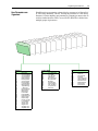
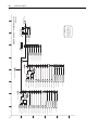
Catalog Number Explanation
See page...
Preface-1
Preface-1
Preface-1
Preface-3
Preface-3
Preface-4
Preface-5
Who Should Use This
Manual
This manual is intended for qualified personnel. You must be able to
program and operate Adjustable Frequency AC Drive devices. In addition,
you must have an understanding of the parameter settings and functions.
You must also understand programmable controllers for the PowerFlex
700S with DriveLogix.
What Is Not In This Manual
Since this User Manual is designed to provide installation and wiring and
basic start-up information for frames 1 - 6 only, the following topics have
not been included:
• Spare Parts Information
• Installation and wiring and start-up instructions for frames 9 - 13
Please refer to the tables below for more information on recommended
documentation.
Recommended
Documentation
The following publications provide general drive information.
Title
Wiring and Grounding for PWM AC
Drives
Safety Guidelines for the
Application, Installation and
Maintenance of Solid State Control
A Global Reference Guide for
Reading Schematic Diagrams
Guarding Against Electrostatic
Damage
Publication
DRIVES-IN001…
Available…
SGI-1.1
100-2.10
8000-4.5.2
www.rockwellautomation.com/
literature
p-2
Overview
The following publications provide detailed PowerFlex® 700S drive
information:
Title
PowerFlex 700S Phase II Reference Manual
PowerFlex 700S Phase II Quick Start - Frames
1-6
PowerFlex 700S Phase II Quick Start - Frames
9-13
PowerFlex 700H/S Drives Installation Manual Frames 9 - 13
Publication
Available…
PFLEX-RM003…
20D-QS002…
20D-QS004…
www.rockwellautomation.com/
literature
PFLEX-IN006…
The following publications provide specific PowerFlex 700S drive features
information:
Title
Installation Instructions - Stegmann Feedback
Option for PowerFlex 700S Drive
Installation Instructions - Resolver Feedback
Option for PowerFlex 700S Drives
Installation Instructions - Multi-Device Interface
for PowerFlex 700S Drive
Installation Instructions - Second Encoder
Option for PowerFlex 700S Drives with Phase II
Control
Firmware Release Notes - PowerFlex 700S
Drive & DriveLogix
Publication
20D-IN001…
Available…
20D-IN002…
20D-IN004…
20D-IN009…
www.rockwellautomation.com/
literature
20D-RN007…
For Allen-Bradley Drives Technical Support:
Title
Allen-Bradley Drives Technical Support
Online at…
www.rockwellautomation.com/literature
or
call M-F, 7:00a.m. to 7:00p.m. Central STD time:
1.262.512.8176
For Automation and Control Technical Support:
Title
Online at…
Rockwell Automation Technical Support http://support.rockwellautomation.com/knowledgebase
The following publications provide necessary information when applying
the DriveLogix Controller.:
Title
DriveLogix5730 Controller User Manual
PowerFlex 700S Drive & DriveLogix Controller
Logix5000 Controllers Common Procedures
Logix5000 Controllers General Instructions
Logix5000 Controllers Process Control and
Drives Instructions
RSLogix 5000 Getting Results
Publication
20D-UM003…
20D-RN007…
1756-PM001…
1756-RM003…
1756-RM006…
9399-RLD300GR
Available…
www.rockwellautomation.com/
literature
Overview
p-3
The following publications provide information that is useful when
planning and installing communication networks:
Title
ContolNet Coax Tap Installation
Instructions
ControlNet Cable System Planning
and Installation Manual
ContolNet Fiber Media Planning
and Installation Guide
Manual Conventions
Publication
1786-5.7
1786-6.2.1
Available…
www.rockwellautomation.com/literature
CNET-IN001…
• In this manual we refer to the PowerFlex 700S Adjustable Frequency AC
Drive as: drive, PowerFlex 700S, PowerFlex 700S drive or PowerFlex
700S AC drive.
• To help differentiate parameter names and LCD display text from other
text, the following conventions will be used:
– Parameter Names will appear in [brackets] after the Parameter
Number.
For example: Par 307 [Output Voltage].
– Display text will appear in “quotes.” For example: “Enabled.”
• The following words are used throughout the manual to describe an
action:
Word
Can
Cannot
May
Must
Shall
Should
Should Not
Drive Frame Sizes
Meaning
Possible, able to do something
Not possible, not able to do something
Permitted, allowed
Unavoidable, you must do this
Required and necessary
Recommended
Not recommended
Similar PowerFlex 700S drive sizes are grouped into frame sizes to simplify
spare parts ordering, dimensioning, etc. A cross reference of drive catalog
numbers and their respective frame size is provided in Appendix A.
p-4
Overview
General Precautions
Class 1 LED Product
!
!
!
!
!
!
!
!
ATTENTION: Hazard of permanent eye damage exists when
using optical transmission equipment. This product emits intense
light and invisible radiation. Do not look into module ports or
fiber optic cable connectors.
ATTENTION: This drive contains ESD (Electrostatic
Discharge) sensitive parts and assemblies. Static control
precautions are required when installing, testing, servicing or
repairing this assembly. Component damage may result if ESD
control procedures are not followed. If you are not familiar with
static control procedures, reference A-B publication 8000-4.5.2,
“Guarding Against Electrostatic Damage” or any other applicable
ESD protection handbook.
ATTENTION: An incorrectly applied or installed drive can
result in component damage or a reduction in product life. Wiring
or application errors, such as, undersizing the motor, incorrect or
inadequate AC supply, or excessive ambient temperatures may
result in malfunction of the system.
ATTENTION: Only qualified personnel familiar with the
PowerFlex 700S Drive and associated machinery should plan or
implement the installation, start-up and subsequent maintenance
of the system. Failure to comply may result in personal injury
and/or equipment damage.
ATTENTION: To avoid an electric shock hazard, verify that the
voltage on the bus capacitors has discharged before performing
any work on the drive. Measure the DC bus voltage at the +DC &
–DC terminals of the Power Terminal Block (refer to Chapter 1
for location). The voltage must be zero.
ATTENTION: Risk of injury or equipment damage exists. DPI
or SCANport host products must not be directly connected
together via 1202 cables. Unpredictable behavior can result if two
or more devices are connected in this manner.
ATTENTION: Risk of injury or equipment damage exists.
Parameters 365 [Fdbk LsCnfg Pri] - 394 [VoltFdbkLossCnfg] let
you determine the action of the drive in response to operating
anomalies. Precautions should be taken to ensure that the settings
of these parameters do not create hazards of injury or equipment
damage.
ATTENTION: Risk of injury or equipment damage exists.
Parameters 383 [SL CommLoss Data] - 392 [NetLoss DPI Cnfg]
let you determine the action of the drive if communications are
disrupted. You can set these parameters so that the drive continues
to run. Precautions should be taken to ensure that the settings of
these parameters do not create hazards of injury or equipment
damage.
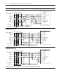
Overview
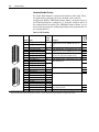
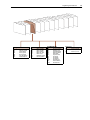
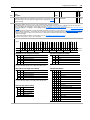
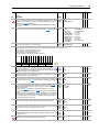
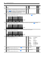
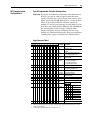
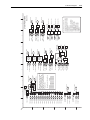
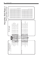
Catalog Number Explanation
Position
1-3
20D
4
5-7
8
9
10
11
12
13
14
15
16
17
D
2P1
A
0
E
Y
N
A
N
A
N
E
b
c
d
e
f
g
h
i
j
k
l
m
a
a
c2
c3
Drive
ND Rating
ND Rating
400V, 50 Hz Input
Code
Type
20D
PowerFlex 700S
b
Voltage Rating
Code
Voltage
Ph.
Prechg.
480V, 60 Hz Input
Code
Amps
kW
Code
Amps
Hp
2P1
2.1
0.75
2P1
2.1
1.0
3P5
3.5
1.5
3P4
3.4
2.0
5P0
5.0
2.2
5P0
5
3.0
8P7
8.7
4.0
8P0
8
5.0
011
11.5
5.5
011
11
7.5
015
15.4
7.5
014
14
10
022
22
11
022
22
15
030
30
15
027
27
20
B§
240V ac
3
⎯
C§
400V ac
3
⎯
D§
480V ac
3
⎯
E♣§
600V ac
3
⎯
037
37
18.5
034
34
25
F
690V ac
3
⎯
043
43
22
040
40
30
H
540V dc
⎯
N
056
56
30
052
52
40
J
650V dc
⎯
N
072
72
37
065
65
50
K
810V dc
⎯
N
085
85
45
077
77
60
M
932V dc
⎯
N
105
105
55
096
96
75
N
325V dc
⎯
Y
125
125
55
125
125
100
P
540V dc
⎯
Y
170
170
90
156
156
125
R
650V dc
⎯
Y
205
205
110
180
180
150
T
810V dc
⎯
Y
260
260
132
248
248
200
⎯
Y
261
261
132
261
261
200
♣ Note: CE Certification testing has not been
performed on 600V class drives, Frames 1…4.
Frames 5 & 6 Only.
300
300
160
300
300
250
385
385
200
385
385
300
460
460
250
460
460
350
Frames 5 & up.
§ For DC input on Frames 1…4, use the
corresponding AC input code B, C, D, or E.
500
500
250
500
500
450
590
590
315
590
590
500
650
650
355
650
650
500
730
730
400
730
730
600
820
820
450
820
820
700
920
920
500
920
920
800
1K0
1030
560
1K0
1030
900
W
932V dc
c1
ND Rating
208/240V, 60Hz Input
208V
Amps
240V
Amps
1K1
1150
630
1K1
1150
1000
Code
Hp
1K3
1300
710
1K3
1300
1200
4P2
4.8
4.2
1.0
1K4
1450
800
1K4
1450
1250
6P8
7.8
6.8
2.0
9P6
11
9.6
3.0
015
17.5
15.3
5.0
022
25.3
22
7.5
028
32.2
28
10
042
48.3
42
15
052
56
52
20
070
78.2
70
25
080
92
80
30
104
120
104
40
130
130
130
50
154
177
154
60
192
221
192
75
260
260
260
100
p-5
p-6
Overview
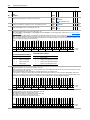
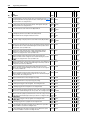
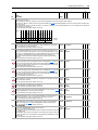
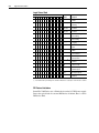
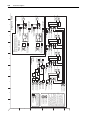
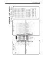
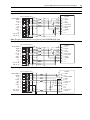
Catalog Number Explanation, Cont’d
c4
c5
j
ND Rating
ND Rating
Comm Slot
600V, 60Hz Input ♣
690V, 50 Hz Input ♣
Code
Version
Code
Amps
Hp
Code
Amps
kW
N
None
1P7
1.7
1
052
52
45
C
DPI ControlNet (Coax)
2P7
2.7
2
060
60
55
D
DPI DeviceNet
3P9
3.9
3
082
82
75
E
DPI EtherNet/IP
6P1
6.1
5
098
98
90
R
DPI RIO
9P0
9
7.5
119
119
110
S
DPI RS-485 DF1
011
11
10
142
142
132
1
DriveLogix ControlNet (Coax)
017
17
15
170
170
160
2
022
22
20
208
208
200
DriveLogix ControlNet Redundant
(Coax)
027
27
25
261
261
250
3
DriveLogix ControlNet (Fiber)
032
32
30
325
325
315
4
041
41
40
385
385
355
DriveLogix ControlNet Redundant
(Fiber)
052
52
50
416
416
400
5
DriveLogix DeviceNet (Open Conn.)
062
62
60
460
460
450
6
DriveLogix EtherNet/IP
077
77
75
502
502
500
099
99
100
590
590
560
125
125
125
650
650
630
144
144
150
750
750
710
170
170
150
820
820
800
208
208
200
920
920
900
261
261
250
1K0
1030
1000
325
325
350
1K1
1180
1100
385
385
400
♣ Note: CE Certification testing has not been
performed on 600V class drives Frames 1…4.
416
416
450
460
460
450
502
502
500
f
590
590
600
Documentation
650
650
700
750
750
800
E
Quick Start Guide
820
820
900
N
No Documentation
Code
Documents
920
920
1000
1K0
1030
1100
g
1K1
1180
1300
Brake
♣ Note: CE Certification testing has not been
performed on 600V class drives Frames 1…4.
d
Enclosure
Enclosure
A
IP20, NEMA Type 1
N
Open/IP00
Code
w/Brake IGBT ‡
Y
Yes
N
No
A
No
No
Expanded
B
Phase
II
No
Yes
Expanded
C
Phase
II
Yes
No
Expanded
D
Phase
II
Yes
Yes
Expanded
G
Phase
II
N/A
No
Slim
H
Phase
II
N/A
Yes
Slim
Feedback
Code
Option
N
No Option
A
Resolver
B
Stegman Hi-Resolution Encoder
C
Multi-Device Interface
2nd Encoder
Brake Resistor
S
Safe-Off (w/2nd Encoder)
w/Resistor
Expanded cassette required.
One encoder interface is included with the
base drive.
Yes
N
No
Not available for Frame 3 drives or larger.
HIM
m
i
Code
Operator Interface
0
Blank Cover
2
Digital LCD
Code
3
Full Numeric LCD
5
Prog. Only LCD
C
Full Numeric LCD,
Door Mount Frames 10 & up only.
Cassette
Phase
II
E
Y
e
Control
Logic
Synch
Option Expansion -Link
h
Code
Frames 9 & up Only.
Code
l
‡ Brake IGBT is standard on Frames 1-3 and
optional on Frames 4-9 ONLY.
Code
k
Control Options
Additional Config.
Emission
CE Filter ♣
CM Choke
A
Yes
Yes
B
Yes
No
N§
No
No
Frames 1-6 Only.
Frames 9 & up Only.
§ For use on a high resistive ground or
ungrounded distribution system (Frame 9 only).
♣ Note: CE Certification testing has not been
performed on 600V class drives Frames 1…4.
Code
Description
E
Phase II Control
K
Phase II DriveLogix5730
L
Phase II DriveLogix5730
w/EtherNet/IP
This is an embedded EtherNet option that is
only available with DriveLogix5730.
Chapter
1
Installation/Wiring
Chapter Objectives
This chapter provides the information needed to mount and wire
PowerFlex® 700S AC drives, frames 1 - 6. For installation instructions for
PowerFlex 700S AC drives frames 9 - 13, refer to publication
PFLEX-IN006.
For Information on …
Opening the Cover
Mounting Clearances
AC Supply Source Considerations
Grounding Requirements
Fuses and Circuit Breakers
Power Wiring
Using Input/Output Contactors
Using PowerFlex® 700S Drives with Regenerative Power Units
Disconnecting MOVs and Common Mode Capacitors
I/O Wiring
CE Conformity
See Page...
1-2
1-3
1-4
1-5
1-6
1-7
1-16
1-16
1-17
1-19
1-29
Since most start-up difficulties are the result of incorrect wiring, take every
precaution to assure the wiring is correct. Read and understand all items in
this chapter before beginning installation.
!
ATTENTION: The following information is merely a guide for
proper installation. The Allen-Bradley Company cannot assume
responsibility for the compliance or the noncompliance to any
code, national, local or otherwise for the proper installation of this
drive or associated equipment. A hazard of personal injury and/or
equipment damage exists if codes are ignored during installation.
1-2
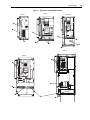
Installation/Wiring
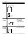
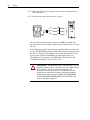
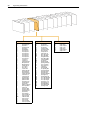
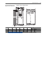
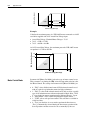
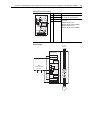
Opening the Cover
Frames 1-4
Locate the slot in the upper left corner. Slide
the locking tab up and swing the cover open.
Special hinges allow cover to move away from
drive and lay on top of adjacent drive (if
present).
Frame 5
Slide the locking tab up, loosen the right-hand
cover screw and remove.
Frame 6
Loosen 2 screws at bottom of drive cover.
Carefully slide bottom cover down & out.
Loosen the 2 screws at top of cover and
remove.
(x2)
Proper tightening
torque for reassembly
is 6 lb.-in.
(x2)
=
1
BR 2
BR
PE
L2
DC
DC- +
U/
V/ T1
W T2
R/L1 /T3
(x3)
=
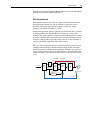
Removing the Side Covers
Removing the Cassette
Task
A
B
C
Description
Open the door of the power structure and disconnect the cables that
connect to the main board
Loosen screws on face of cassette
Remove the cassette
Task
A
B
Description
Loosen screws on face of front cover and remove the cover
Loosen screws on side of rear cover and remove the cover
Installation/Wiring
1-3
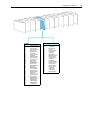
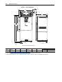
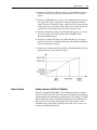
Mounting Clearances
101.6mm
(4.0 in.)
No Adhesive Label
(see below)
With Adhesive Label
50.8mm (2.0 in.)
101.6mm
(4.0 in.)
50.8mm (2.0 in.)
101.6mm
(4.0 in.)
(see below)
101.6mm
(4.0 in.)
Operating Temperatures
Refer to the Drive, Fuse and Circuit Breaker Ratings tables in Appendix A
for information on drive ambient operating temperatures.
1-4
Installation/Wiring
AC Supply Source
Considerations
PowerFlex drives are suitable for use on a circuit capable of delivering up to
a maximum of 200,000 rms symmetrical amperes, 600 volts with
recommended fuses/circuit breakers. Refer to the PowerFlex Reference
Manual - Phase II Control, publication PFLEX-RM003, for actual interrupt
ratings based on circuit breaker or fuse choice.
!
ATTENTION: To guard against personal injury and/or
equipment damage caused by improper fusing or circuit breaker
selection, use only the recommended line fuses/circuit breakers
specified in Appendix A.
If a Residual Current Detector (RCD) is used as a system ground fault
monitor, only Type B (adjustable) devices should be used to avoid nuisance
tripping.
Unbalanced, Ungrounded or Resistive Grounded Distribution Systems
If phase to ground voltage will exceed 125% of normal or the supply system
is ungrounded, refer to Wiring and Grounding Guidelines for Pulse Width
Modulated (PWM) AC Drives, publication DRIVES-IN001, for more
information.
!
ATTENTION: PowerFlex 700S drives contain protective MOVs
and common mode capacitors that are referenced to ground.
These devices must be disconnected if the drive is installed on a
resistive grounded distribution system or an ungrounded
distribution system. See page page 1-18 for jumper locations.
Installation/Wiring
1-5
Input Power Conditioning
Certain events on the power system supplying a drive can cause component
damage or shortened product life. These conditions are divided into 2 basic
categories:
1. All Drives
– The power system has power factor correction capacitors switched in
and out of the system, either by the user or by the power company.
– The power source has intermittent voltage spikes in excess of 6000
volts. These spikes could be caused by other equipment on the line or
by events such as lightning strikes.
– The power source has frequent interruptions.
2. 5 HP or Less Drives (in addition to “1” above)
– The nearest supply transformer is larger than 100kVA or the available
short circuit (fault) current is greater than 100,000A.
– The impedance in front of the drive is less than 0.5%.
If any or all of these conditions exist, it is recommended that the user install
a minimum amount of impedance between the drive and the source. This
impedance could come from the supply transformer itself, the cable
between the transformer and drive or an additional transformer or reactor.
The impedance can be calculated using the information supplied in the
technical document Wiring and Grounding Guidelines for Pulse Width
Modulated (PWM) AC Drives, publication DRIVES-IN001.
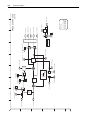
Grounding Requirements
The drive Safety Ground-PE must be connected to system ground.
Ground impedance must conform to the requirements of national and local
industrial safety regulations and/or electrical codes. The integrity of all
ground connections should be periodically checked.
Recommended Grounding Scheme
A single point (PE only) grounding scheme should be used. Some
applications may require alternate grounding schemes, refer to the Wiring
and Grounding Guidelines for pulse Width Modulated (PWM) AC Drives,
publication number DRIVES-IN001, for more information. These
applications include installations with long distances between drives or
drive line-ups, which could cause large potential differences between the
drive or line-up grounds.
For installations within a cabinet, a single safety ground point or ground bus
bar connected directly to building steel should be used. All circuits
including the AC input ground conductor should be grounded
independently and directly to this point/bar.
1-6
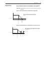
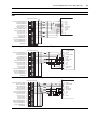
Installation/Wiring
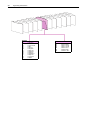
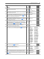
Figure 1.1 Typical Grounding
R
(L1)
S
(L2)
T
(L3)
PE
U
(T1)
V
(T2)
W
(T3)
DC
+
DC
–
BR1
BR2
Required
Input Fusing
Required Branch
Circuit Disconnect
Shield Termination - SHLD
The Shield terminal (see Figure 1.3 on page 1-13) provides a grounding
point for the motor cable shield. It must be connected to an earth ground by
a separate continuous lead. The motor cable shield should be connected to
this terminal on the drive (drive end) and the motor frame (motor end). Use
a shield terminating or EMI clamp to connect shield to this terminal.
RFI Filter Grounding
Using an optional RFI filter may result in relatively high ground leakage
currents. Therefore, the filter must only be used in installations with
grounded AC supply systems and be permanently installed and solidly
grounded (bonded) to the building power distribution ground. Ensure that
the incoming supply neutral is solidly connected (bonded) to the same
building power distribution ground. Grounding must not rely on flexible
cables and should not include any form of plug or socket that would permit
inadvertent disconnection. Some local codes may require redundant ground
connections. The integrity of all connections should be periodically
checked. Refer to the instructions supplied with the filter.
Fuses and Circuit Breakers
The PowerFlex 700S can be installed with either input fuses or an input
circuit breaker. Local/national electrical codes may determine additional
requirements for these installations. Refer to Appendix A for recommended
fuses/circuit breakers.
!
ATTENTION: The PowerFlex 700S does not provide input
power short circuit protection. Specifications for the
recommended fuse or circuit breaker to provide drive input power
protection against short circuits are provided in Appendix A.
Installation/Wiring
Power Wiring
1-7
Since most start-up difficulties are the result of incorrect wiring, take every
precaution to assure the wiring is correct. Read and understand all items in
this section before beginning installation.
!
ATTENTION: The following information is merely a guide for
proper installation. The Allen-Bradley Company cannot assume
responsibility for the compliance or the noncompliance to any
code, national, local or otherwise for the proper installation of this
drive or associated equipment. A hazard of personal injury and/or
equipment damage exists if codes are ignored during installation.
Power Cable Types Acceptable for 200-600 Volt Installations
!
ATTENTION: National Codes and standards (NEC, BSI etc.)
and local codes outline provisions for safely installing electrical
equipment. Installation must comply with specifications
regarding wire types, conductor sizes, branch circuit protection
and disconnect devices. Failure to do so may result in personal
injury and/or equipment damage.
A variety of cable types are acceptable for drive installations. For many
installations, unshielded cable is adequate, provided it can be separated
from sensitive circuits. As an approximate guide, allow a spacing of 0.3
meters (1 foot) for every 10 meters (32.8 feet) of length. In all cases, long
parallel runs must be avoided. Do not use cable with an insulation thickness
less than or equal to 15 mils (0.4mm/0.015 in.). Use copper wire only. Wire
gauge requirements and recommendations are based on 75° C. Do not
reduce wire gauge when using higher temperature wire.
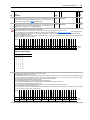
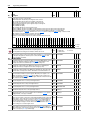
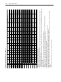
Table 1.A Recommended Cable Design
Type
Type 1
Type 2
Type 3
Type 4
Type 5
Max. Wire Size Where Used
2 AWG
Standard Installations
100 HP or less
2 AWG
Standard Installations
100 HP or less with
Brake Conductors
500 MCM AWG Standard Installations
150 HP or more
500 MCM AWG Water, Caustic Chemical,
Crush Resistance
Rating/Type
600V, 90oC (194oF)
XHHW2/RHW-2
600V, 90oC (194oF)
RHH/RHW-2
Description
Four tinned copper conductors with XLPE insulation
Tray rated 600V, 90oC (194oF)
RHH/RHW-2
Tray rated 600V, 90oC (194oF)
RHH/RHW-2
500 MCM AWG 690V Applications
Tray rated 2000V, 90oC (194oF)
Three tinned copper conductors with XLPE insulation
and (3) bare copper grounds and PVC jacket.
Three bare copper conductors with XLPE insulation and
three copper grounds on #10 AWG and smaller.
Acceptable in Class I & II, Division I & II locations.
Three tinned copper conductors with XLPE insulation. (3)
bare copper grounds and PVC jacket.
Note: If terminator network or output filter is used,
connector insulation must be XLPE, not PVC.
Four tinned copper conductors with XLPE insulation plus
one (1) shielded pair of brake conductors.
1-8
Installation/Wiring
Unshielded
THHN, THWN or similar wire is acceptable for drive installation in dry
environments provided adequate free air space and/or conduit fill rates
limits are provided. Do not use THHN or similarly coated wire in wet
areas. Any wire chosen must have a minimum insulation thickness of 15
Mils and should not have large variations in insulation concentricity.
Shielded/Armored Cable
Shielded cable contains all of the general benefits of multi-conductor cable
with the added benefit of a copper braided shield that can contain much of
the noise generated by a typical AC Drive. Strong consideration for shielded
cable should be given in installations with sensitive equipment such as
weigh scales, capacitive proximity switches and other devices that may be
affected by electrical noise in the distribution system. Applications with
large numbers of drives in a similar location, imposed EMC regulations or a
high degree of communications/networking are also good candidates for
shielded cable.
Shielded cable may also help reduce shaft voltage and induced bearing
currents for some applications. In addition, the increased impedance of
shielded cable may help extend the distance the motor can be located from
the drive without the addition of motor protective devices such as terminator
networks. Refer to “Reflected Wave” in Wiring and Grounding Guidelines
for Pulse Width Modulated (PWM) AC Drives, publication DRIVES-IN001.
Consideration should be given to all of the general specifications dictated by
the environment of the installation, including temperature, flexibility,
moisture characteristics and chemical resistance. In addition, a braided
shield should be included and specified by the cable manufacturer as having
coverage of at least 75%. An additional foil shield can be greatly improve
noise containment.
A good example of recommended cable is Belden® 295xx (xx determines
gauge). This cable has 4 XLPE insulated conductors with a 100% coverage
foil and an 85% coverage copper braided shield (with drain wire)
surrounded by a PVC jacket.
Other types of shielded cable are available, but the selection of these types
may limit the allowable cable length. Particularly, some of the newer cables
twist 4 conductors of THHN wire and wrap them tightly with a foil shield.
This construction can greatly increase the cable charging current required
and reduce the overall drive performance. Unless specified in the individual
distance tables as tested with the drive, these cables are not recommended
and their performance against the lead length limits supplied is not known.
EMC Compliance
Refer to CE Conformity on page 1-29 for details.
Installation/Wiring
1-9
Cable Trays and Conduit
If cable trays or large conduits are to be used, refer to guidelines presented
in publication DRIVES-IN001. . . , Grounding and Wiring Guidelines for
Pulse Width Modulated (PWM) AC Drives.
!
ATTENTION: To avoid a possible shock hazard caused by
induced voltages, unused wires in the conduit must be grounded
at both ends. For the same reason, if a drive sharing a conduit is
being serviced or installed, all drives using this conduit should be
disabled. This will help minimize the possible shock hazard from
“cross coupled” motor leads.
Motor Cable Lengths
Typically, motor lead lengths less than 30 meters (100 feet) are acceptable.
For motor lead lengths of 30 meters (100 feet) or above, applicable cable
types and length recommendations and restrictions, refer to publication
20D-TD002 . . . , Technical Data - PowerFlex 700S Drives - Phase II
Control, or publication DRIVES-IN001..., Grounding and Wiring
Guidelines for Pulse Width Modulated (PWM) AC Drives.
Power Terminal Blocks
Figure 1.3 on page 1-13 shows the typical location of the Power Terminal
Block in PowerFlex 700S frame 1 - 6 drives.
Cable Entry Plate Removal
If additional wiring access is needed, the Cable Entry Plate on Frame 1-3
drives can be removed. Simply loosen the screws securing the plate to the
chassis. The slotted mounting holes assure easy removal.
Important: Removing the Cable Entry Plate limits the maximum
surrounding air temperature to 40o C (104o F).
1-10
Installation/Wiring
Power Wiring Access Panel Removal
!
Frame
1, 2 & 6
3
4
5
ATTENTION: Removing the access panel/cover exposes
dangerous voltages on the terminals and negates the enclosure
type rating. Replace the access panel/cover when service is
complete. Failure to comply may result in personal injury or
equipment damage.
Removal Procedure (Replace when wiring is complete)
Remove part of the front cover, see page 1-2.
Open front cover and gently tap/slide the cover down and out.
Loosen the 4 screws and remove.
Remove front cover (see page 1-2), gently tap/slide panel up and out.
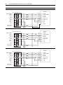
AC Input Phase Selection (Frames 5 & 6 Only)
!
ATTENTION: To avoid a shock hazard, ensure that all
power to the drive has been removed before performing
the following.
Moving the “Line Type” jumper shown in Figure 1.2 on page 1-11 will
select single or three-phase operation. Remove plastic guard to access
jumper.
Important: When selecting single-phase operation, input power must be
applied to the R (L1) and S (L2) terminals only.
Cooling Fan Voltage
Common Bus drives require user supplied 120 or 240V AC to power the
cooling fans. The power source is connected between “0V AC” and the
terminal corresponding to your source voltage (see Figure 1.4 on
page 1-14).
Table 1.B Fan VA Rating
Frame
5
6
Fan Voltage(120V or 240V)
100 VA
138 VA
Selecting/Verifying Fan Voltage (Frames 5 & 6 Only)
!
ATTENTION: To avoid a shock hazard, ensure that all
power to the drive has been removed before performing
the following:
Frames 5 & 6 utilize a transformer to match the input line voltage to the
internal fan voltage. If your line voltage is different than the voltage class
specified on the drive nameplate, it may be necessary to change the
transformer taps. The taps are shown in Figure 1.2 on page 1-11.
Installation/Wiring
1-11
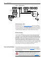
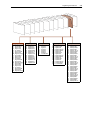
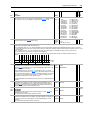
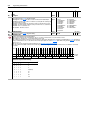
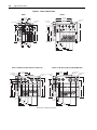
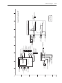
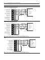
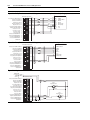
Figure 1.2 Frames 5 & 6 Jumper and Transformer Locations (Frame 5 shown)
Phase Selection
Jumper
3-PH 1-PH
LINE
TYPE
SPARE 1
SPARE 2
Optional
Communications
Module
Fan Voltage
300 VDC EXT PWR SPLY TERM (PS+, PS-)
POWER TERMINAL RATINGS
WIRE RANGE: 14-1/0 AWG (2.5-35 MM2)
TORQUE: 32 IN-LB (3.6 N-M)
STRIP LENGTH: 0.67 IN (17 MM)
USE 75 C CU WIRE ONLY
WIRE RANGE: 22-10 AWG (0.5-4 MM2)
TORQUE: 5.3 IN-LB (0.6 N-M)
STRIP LENGTH: 0.35 IN (9 MM)
9
17
GROUND TERMINAL RATINGS (PE)
WIRE RANGE: 6-1/0 AWG (16-35 MM2)
TORQUE: 44 IN-LB (5 N-M)
STRIP LENGTH: 0.83 IN (21 MM)
21
OUTPUT
INPUT AC
690 Volt Tap
600 Volt Tap
480 Volt Tap
400 Volt Tap
Frame 6 Transformer Tap Access
The transformer is located behind the Power Terminal Block in the area
shown in Figure 1.2. Gain access by releasing the terminal block from the
rail. To release terminal block and change tap:
1. Locate the small metal tab at the bottom of the end block.
2. Press the tab in and pull the top of the block out. Repeat for next block if
desired.
3. Select appropriate transformer tap.
4. Replace block(s) in reverse order.
1-12
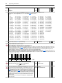
Installation/Wiring
Important Common Bus (DC Input) Application Notes
1. If drives without internal precharge are used (Frames 5 & 6 only), then:
– precharge capability must be provided in the system to guard against
possible damage, and
– disconnect switches Must Not be used between the input of the drive
and a common DC bus without the use of an external precharge
device.
2. If drives with internal precharge (Frames 1-6) are used with a disconnect
switch to the common bus, then an auxiliary contact on the disconnect
must be connected to a digital input of the drive. The corresponding
input (parameter 825-830) must be set to “Precharge Enable”. This
provides the proper precharge interlock, guarding against possible
damage to the drive when connected to a common DC bus.
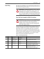
Table 1.C Power Terminal Block Specifications
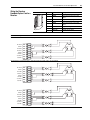
No. Name
Frame
➊ Power Terminal Block 1
Description
Input power and motor
connections
Input power and motor
connections
Input power and motor
connections
BR1, BR2
Wire Size Range(1)
Torque
Maximum
Terminal Bolt Size(2)
Minimum
Maximum
4.0 mm2
(10 AWG)
2
10.0 mm2
(6 AWG)
3
25.0 mm2
(3 AWG)
10.0 mm2
(6 AWG)
4
Input power and motor
35.0 mm2
connections
(1/0 AWG)
R, S, T, BR1, BR2, DC+, 50.0 mm2
5
(3) DC-, U, V and W
(1/0 AWG)
(75 HP)
PE
50.0 mm2
(1/0 AWG)
5
R, S, T, DC+, DC-, U, V and 70.0 mm2
(100 HP)(3) W
(2/0 AWG)
BR1, BR2
50.0 mm2
(1/0 AWG)
PE
50.0 mm2
(1/0 AWG)
6
Input power and motor
120.0 mm2
connections
(4/0 AWG)(5)
0.5 mm2
(22 AWG)
0.8 mm2
(18 AWG)
2.5 mm2
(14 AWG)
0.8 mm2
(18 AWG)
10 mm2
(8 AWG)
2.5 mm2
(14 AWG)
4.0 mm2
(12 AWG)
16.0 mm2
(6 AWG)
2.5 mm2
(14 AWG)
4.0 mm2
(12 AWG)
2.5 mm2
(14 AWG)
1.7 N-m
0.8 N-m
(15 lb.-in.) (7 lb.-in.)
1.7 N-m
1.4 N-m
(15 lb.-in.) (12 lb.-in.)
3.6 N-m
1.8 N-m
(32 lb.-in.) (16 lb.-in.)
1.7 N-m
1.4 N-m
(15 lb.-in.) (12 lb.-in.)
4.0 N-m
4.0 N-m
(24 lb.-in.) (24 lb.-in.)
See Note (4) See Note (3)
6 N-m
6 N-m
(52 lb.-in.) (52 lb.-in.)
—
➋ SHLD Terminal
1-6
Terminating point for wiring —
shields
—
1.6 N-m
1.6 N-m
(14 lb.-in.) (14 lb.-in.)
M12
➌ AUX Terminal Block
1-4
Auxiliary Control Voltage (6) 1.5 mm2
PS+, PS(16 AWG)
4.0 mm2
(10 AWG)
User Supplied Fan Voltage 4.0 mm2
0V AC, 120V AC, 240V AC (10 AWG)
0.2 mm2
(24 AWG)
0.5 mm2
(22 AWG)
0.5 mm2
(22 AWG)
—
—
—
0.6 N-m
(5.3 lb.-in.)
0.6 N-m
(5.3 lb.-in.)
0.6 N-m
(5.3 lb.-in.)
0.6 N-m
(5.3 lb.-in.)
—
5-6
➍ Fan Terminal Block
(Common Bus Only)
(1)
(2)
(3)
(4)
(5)
(6)
5-6
Recommended
—
—
—
—
—
—
—
—
—
—
M10
Maximum/minimum sizes that the terminal block will accept - these are not recommendations.
Apply counter torque to the nut on the other side of terminations when tightening or loosening the terminal bolt in order to avoid damage to the terminal.
Not all terminals present on all drives.
Refer to the terminal block label inside the drive.
If necessary, two wires can be used in parallel to any of these terminals using two lugs.
Auxiliary power: UL Installation - 300V DC, ±10%, Non UL Installation - 270-600V DC, ±10%. Frame 1-6, 100 W.
Installation/Wiring
1-13
Figure 1.3 Typical Power Terminal Block Location
Frame 2
Frame 1
Frame 3 & 4
➌
DANGER
!
Optional
Communications
Module
Use 75C Wire Only
#10-#14 AWG
Optional
Communications
Module
Torque to 7 in-lbs
BR1
BR2
PE B
DC+
WIRE
STRIP
BR1 B
V/T2
V/T2 W/T3
PE A
PE R/L1 S/L2 T/L3
W/T3
WIRE
STRIP
AUX IN+ AUX OUT–
BR1 BR2
75C Cu Wire
6 AWG [10MM2] Max.
R/L1
S/L2
SHLD
SHLD
75C Cu Wire
3 AWG [25MM2] Max.
16 IN. LBS.
1.8 N-M } TORQUE
12 IN. LBS.
1.4 N-M } TORQUE
➊
T/L3
AUX IN
+ –
POWER
U/T1
75C Cu Wire
2
6 AWG [10MM ] Max.
12 IN. LBS.
1.4 N-M } TORQUE
POWER
➌
PE
CONTROL
DC–
CONTROL
➊
BR1 BR2 DC+ DC- U/T1 V/T2 W/T3 R/L1 S/L2 T/L3
SHLD
➊
➋
SHLD
/
➋
Frame 6
Frame 5
➋
➋
Optional
Communications
Module
Optional
Communications
Module
300 VDC EXT PWR SPLY TERM (PS+, PS-)
POWER TERMINAL RATINGS
WIRE RANGE: 14-1/0 AWG (2.5-35 MM2)
TORQUE: 32 IN-LB (3.6 N-M)
STRIP LENGTH: 0.67 IN (17 MM)
USE 75 C CU WIRE ONLY
WIRE RANGE: 6-1/0 AWG (16-35
TORQUE: 44 IN-LB (5 N-M)
STRIP LENGTH: 0.83 IN (21 MM)
WIRE RANGE: 22-10 AWG (0.5-4 MM2)
TORQUE: 5.3 IN-LB (0.6 N-M)
STRIP LENGTH: 0.35 IN (9 MM)
9
17
GROUND TERMINAL RATINGS (PE)
MM2)
21
OUTPUT
INPUT AC
➌
PS+
PS–
WIRE STRIP
➌
22-10
AWG
5.3 IN-LB
(0.6 N-M)
BR2
BR1
DC+
DC–
USE 75 C COPPER WIRE ONLY, TORQUE 52 IN-LB (6 N-M)
USE 75 C
COPPER WIRE
ONLY
TORQUE
52 IN-LB
(6 N-M)
➊
➊
PE
➋
➍
➊
T1
T2
OUTPUT
T3
L1
L2
INPUT
L3
PE
Installation/Wiring
Figure 1.4 Power Terminal Block
BR1
BR2
DC+
DC–
PE
Frame 2
Frame 1
U (T1)
V (T2)
W (T3)
R (L1)
S (L2)
T (L3)
BR1 BR2 DC+ DC– PE
U V W R S T
(T1) (T2) (T3) (L1) (L2) (L3)
Motor
Frame 3
Input AC Line
BR1 BR2 DC+ DC– U V W R S
T
(T1) (T2) (T3) (L1) (L2) (L3)
BR1/
BR2 DC+ DC+ DC– U/T1 V/T2 W/T3
PS–
PE
PE
R/L1 S/L2 T/L3
Frame 5 - 75 HP, Normal Duty
480V AC Input
PS+
BR2
BR1/
DC+
DC+
DC–
U/T1
V/T2
R/L1
W/T3
PE
S/L2
T/L3
PE
PS–
Frame 5 - 100 HP, Normal Duty
480V AC Input
PS+
BR1*/
BR2* DC+ DC+ DC–
PS–
U/T1 V/T2 W/T3
0 240
VAC VAC
PE
PE
Frame 5 - 75 HP, Normal Duty
650V DC Input
120
VAC
PS+
Precharge Resistor Fuse – FWP-15A14F
(Common Bus Drives w/Precharge Only)
BR1*/
BR2* DC+
PS–
DC+
DC–
U/T1
V/T2
W/T3
0 240
PEVAC VAC
PE
Frame 5 - 100 HP, Normal Duty
650V DC Input
120
VAC
PS+
Precharge Resistor Fuse – FWP-15A14F
(Common Bus Drives w/Precharge Only)
Frame 6 - 150 HP, Normal Duty
650V DC Input
Common Mode Capacitor
PS+
PS–
WIRE STRIP
Frame 6 - 150 HP, Normal Duty
480 V AC Input
& MOV Jumpers
22-10
AWG
5.3 IN-LB
(0.6 N-M)
BR2
BR1
DC+
DC–
Input Filter Capacitor
PS+
PS–
USE 75 C COPPER WIRE ONLY, TORQUE 52 IN-LB (6 N-M)
WIRE STRIP
22-10
AWG
5.3 IN-LB
(0.6 N-M)
BR2
BR1
DC+
Common Mode Capacitor
& MOV Jumpers
DC–
Precharge Resistor Fuse – FWP-15A14F
(Common Bus Drives w/Precharge Only)
USE 75 C COPPER WIRE ONLY, TORQUE 52 IN-LB (6 N-M)
USE 75 C
COPPER WIRE
ONLY
TORQUE
52 IN-LB
(6 N-M)
TORQUE
52 IN-LB
(6 N-M)
U
T1
V
T2
OUTPUT
W
T3
PE
PE
R
L1
S
L2
INPUT
T
L3
U
T1
V
T2
W
T3
PE
OUTPUT
PE
22-10 AWG
5.3 IN-LB
(0.6 N-M)
0 VAC
1-PHASE
USE 75 C
COPPER WIRE
ONLY
0 VAC
120 VAC
240 VAC
Input Filter Capacitor
FAN
INPUT
1-14
120V AC
240V AC
Shaded terminals (BR1 & BR2) will only be present on drives ordered with the Brake Option.
Installation/Wiring
Terminal
BR1
BR2
DC+
DC–
PE
U
V
W
R
S
T
Description
DC Brake (+)
DC Brake (–)
DC Bus (+)
DC Bus (–)
PE Ground
Motor Ground
U (T1)
V (T2)
W (T3)
R (L1)
S (L2)
T (L3)
Notes
Dynamic Brake Resistor Connection (+)
Dynamic Brake Resistor Connection (–)
DC Input Power or Dynamic Brake Chopper
DC Input Power or Dynamic Brake Chopper
Refer to Figure 1.6 on page 18 for location on 3 Frame drives
Refer to Figure 1.6 on page 18 for location on 3 Frame drives
To motor
To motor
To motor
AC Line Input Power
AC Line Input Power
AC Line Input Power
Dynamic Brake Resistor Considerations
!
1-15
ATTENTION: The drive does not offer protection for
externally mounted brake resistors. A risk of fire exists if
external braking resistors are not protected. External resistor
packages must be self-protected from over temperature or a
circuit equivalent to the one shown below must be supplied.
Figure 1.5 External Brake Resistor Circuitry
Three-Phase
AC Input
(Input Contactor) M
R (L1)
S (L2)
T (L3)
Power Off
Power On
M
M
Power Source
DB Resistor Thermostat
1-16
Installation/Wiring
Using Input/Output
Contactors
!
!
!
Using PowerFlex® 700S
Drives with Regenerative
Power Units
ATTENTION: A contactor or other device that routinely
disconnects and reapplies the AC line to the drive to start and stop
the motor can cause drive hardware damage. The drive is
designed to use control input signals that will start and stop the
motor. If an input device is used occasionally, an auxiliary contact
on that device should also be wired to a digital input programmed
as a “Enable” function. The input device must not exceed one
operation per minute or drive damage will occur.
ATTENTION: The drive start/stop control circuitry includes
solidstate components. If hazards due to accidental contact with
moving machinery or unintentional flow of liquid, gas or solids
exist, an additional hardwired stop circuit may be required to
remove the AC line to the drive. When the AC line is removed,
there will be a loss of any inherent regenerative braking effect that
might be present - the motor will coast to a stop. An auxiliary
braking method may be required.
ATTENTION: To guard against drive damage when using
output contactors, the following information must be read and
understood. One or more output contactors may be installed
between the drive and motor(s) for the purpose of disconnecting
or isolating certain motors/loads. If a contactor is opened while
the drive is operating, power will be removed from the respective
motor, but the drive will continue to produce voltage at the output
terminals. In addition, reconnecting a motor to an active drive (by
closing the contactor) could produce excessive current that may
cause the drive to fault. If any of these conditions are determined
to be undesirable or unsafe, an auxiliary contact on the output
contactor should be wired to a drive digital input that is
programmed as “Enable.” This will cause the drive to execute a
coast-to-stop (cease output) whenever an output contactor is
opened.
If a Regenerative unit (i.e., 1336 REGEN) is used as a bus supply or a brake,
the common mode capacitors should be disconnected (see Table 1.D on
page 1-17).
Regenerative Unit to Drive Connections
Regenerative Brake Mode
Terminals
Frame(s) 1336 REGEN
1- 4
DC+ & DC5&6
DC+ & DC-
PowerFlex 700S
BR1 & DCDC+ & DC-
Regenerative Bus Supply Mode
Terminals
Frame(s) 1336 REGEN
1-4
DC+ & DC5&6
DC+ & DC-
PowerFlex 700S
DC+ & DCDC+ & DC- of the Common Bus Drives
Installation/Wiring
Disconnecting MOVs and
Common Mode Capacitors
1-17
PowerFlex 700S drives contain protective MOVs and common mode
capacitors that are referenced to ground. To guard against drive damage,
these devices must be disconnected if the drive is installed on a resistive
grounded distribution system or an ungrounded distribution system where
the line-to-ground voltages on any phase could exceed 125% of the nominal
line-to-line voltage. To disconnect these devices, remove the jumper(s)
listed in Table 1.D. Jumpers can be removed by carefully pulling the jumper
straight out. See the Grounding and Wiring Guidelines for PWM AC Drives,
publication DRIVES-IN001, for more information on ungrounded system
installation.
!
ATTENTION: To avoid an electric shock hazard, verify that the
voltage on the bus capacitors has discharged before removing/
installing jumpers. Measure the DC bus voltage at the +DC & –
DC terminals of the Power Terminal Block. The voltage must be
zero.
Table 1.D Jumper Removal
Frames Jumper
1
PEA
PEB
2-4
PEA
PEB
5
Wire
Component
Common
Mode
Capacitors
MOV’s
Jumper Location
Remove the Control Assembly and Cassette.
Jumpers are located on the drive Power Board (see
Figure 1.6).
Common
Mode
Capacitors
MOV’s
Jumpers are located above the Power Terminal Block
(see Figure 1.6).
Common
Mode
Capacitors
Remove the I/O Cassette. The green/yellow jumper is
located on the back of chassis in the area shown (see
Figure 1.6). Disconnect, insulate and secure the wire
to guard against unintentional contact with chassis or
components.
Note location of green/yellow jumper wire in Figure
1.6. Disconnect, insulate and secure the wire guard
against unintentional contact with chassis or
components.
Remove the wire guard from the Power Terminal
Block. Disconnect the three green/yellow wires from
the two “PE” terminals shown in Figure 1.4. Insulate
and secure the wires to guard against unintentional
contact with chassis or components.
MOV’s
Input Filter
Capacitors
6
Wire
!
Common
Mode
Capacitors
MOV’s
Input Filter
Capacitors
No.
➊
➋
➌
➍
➎
➏
Please
refer to
Power
Terminal
Blocks,
Frame 6
on page
1-15.
ATTENTION: The disconnecting MOV must be used on a
grounded system.
Installation/Wiring
Figure 1.6 Typical Jumper Locations
Frame 1
(Control Assembly & I/O
Cassette Removed)
➌
Frame 2
➍
PE 1
PE 2
MOV-PE JMPR
PE 4
PE 3
DC FILTER CAP-PE JMPR
!
ly
On
ire
CW G
e 75
Us #14 AW
lbs
#10- 7 into
ue
Torq
AUX IN+ AUX OUT–
BR1
BR2
DC+
DC–
PE
SHLD
U/T1
V/T2
3
W/T
R/L1
S/L2
T/L3
➊
➋
Frames 3 & 4
SHLD
➎
Frame 5
➍
Optional
Communications
Module
Optional
Communications
Module
PE B
PE A
➌
12 IN. LBS.
1.4 N-M } TORQUE
75C Cu Wire
3 AWG [25MM2] Max.
16 IN. LBS.
1.8 N-M } TORQUE
POWER
WIRE
STRIP
BR1 BR2
75C Cu Wire
6 AWG [10MM2] Max.
AUX IN
+ –
BR1 BR2 DC+ DC- U/T1 V/T2 W/T3 R/L1 S/L2 T/L3
300 VDC EXT PWR SPLY TERM (PS+, PS-)
POWER TERMINAL RATINGS
WIRE RANGE: 14-1/0 AWG (2.5-35 MM2)
TORQUE: 32 IN-LB (3.6 N-M)
STRIP LENGTH: 0.67 IN (17 MM)
USE 75 C CU WIRE ONLY
WIRE RANGE: 22-10 AWG (0.5-4 MM2)
TORQUE: 5.3 IN-LB (0.6 N-M)
STRIP LENGTH: 0.35 IN (9 MM)
9
17
GROUND TERMINAL RATINGS (PE)
WIRE RANGE: 6-1/0 AWG (16-35 MM2)
TORQUE: 44 IN-LB (5 N-M)
STRIP LENGTH: 0.83 IN (21 MM)
21
PE
OUTPUT
SHLD
SHLD
➏
INPUT AC
POWER
CONTROL
WIRE
STRIP
75C Cu Wire
6 AWG [10MM2] Max.
12 IN. LBS.
1.4 N-M } TORQUE
ER
NG
DA
CONTROL
1-18
Installation/Wiring
I/O Wiring
1-19
Important points to remember about I/O wiring:
• Always use copper wire.
• Wire with an insulation rating of 600V or greater is recommended.
• Control and signal wires should be separated from power wires by at
least 0.3 meters (1 foot).
• 4100CCF3 Flex I/O cable for use with DriveLogix is 3 ft. maximum
length.
Important: I/O terminals labeled “(–)” or “Common” are not referenced to
earth ground and are designed to greatly reduce common mode
interference. Grounding these terminals can cause signal noise.
!
ATTENTION: Hazard of personal injury or equipment damage
exists when using bipolar input sources. Noise and drift in sensitive
input circuits can cause unpredictable changes in motor speed and
direction. Use speed command parameters to help reduce input
source sensitivity.
Table 1.E Recommended Control Wire
Type
Digital I/O
Wire Type(s)
Un-shielded Per US NEC or applicable
national or local code
Shielded
Multi-conductor shielded cable
such as Belden 8770(or equiv.)
Belden 8760/9460(or equiv.)
Description
–
Signal:
0.196 mm2 (24AWG),
individually shielded.
0.750 mm2 (18AWG)
0.750 mm2 (18AWG),
individually shielded pair.
Insulation
Rating
300V, 60o C
(140o F),
Minimum
0.750 mm2 (18AWG), 3
conductor, shielded.
Standard
0.750 mm2 (18AWG),
Analog I/O
twisted pair, 100% shield
with drain (5).
Remote Pot Belden 8770(or equiv.)
0.750 mm2 (18AWG), 3
cond., shielded
Encoder/
Combined: Belden 9730 (or equivalent) (1) 0.196 mm2 (24AWG),
Pulse I/O
individually shielded.
Less 30.5 m
(100 ft.)
300V,
0.196 mm2 (24AWG),
Encoder/
Signal:
Belden 9730/9728 (or
75-90 ºC
(1)
individually shielded.
Pulse I/O
equivalent)
(167-194 ºF)
(2)
2
30.5 m (100 Power:
0.750 mm (18AWG)
Belden 8790
ft.) to 152.4 Combined: Belden 9892 (3)
0.330 mm2 or 0.500 mm2
m (500 ft.)
(3)
Encoder/
Pulse I/O
152.4 m
(500 ft.) to
259.1 m
(850 ft.)
EMC
Compliance
(1)
(2)
(3)
(4)
(5)
Power:
Combined:
Belden 9730/9728 (or
equivalent) (1)
Belden 8790 (2)
Belden 9773/9774 (or
equivalent) (4)
Refer to CE Conformity on page 1-29 for details.
Belden 9730 is 3 individually shielded pairs (2 channel plus power). If 3 channel is required, use Belden 9728
(or equivalent).
Belden 8790 is 1 shielded pair.
Belden 9892 is 3 individually shielded pairs (3 channel), 0.33 mm2 (22 AWG) plus 1 shielded pair 0.5 mm2 (20
AWG) for power.
Belden 9773 is 3 individually shielded pairs (2 channel plus power). If 3 channel is required, use Belden 9774
(or equivalent).
If the wires are short and contained within a cabinet which has no sensitive circuits, the use of shielded wire
may not be necessary, but is always recommended.
1-20
Installation/Wiring
ATEX Approved Drives and Motors
For detailed information on using ATEX approved drives and motors, refer
to Appendix J.
Wiring the Main Control Board I/O Terminals
Terminal blocks TB1 and TB2 contain connection points for all inputs,
outputs and standard encoder connections. Both terminal blocks reside on
the Main Control Board.
Remove the terminal block plug from the socket, and make connections. Do
not use a tool for terminal block removal. Damage may occur if a tool is
used.
Important: For NEMA/UL Type 1 applications, all wiring must be routed
through the conduit plate on the drive. Route any wires from the
expanded cassette to the base cassette and out of the drive.
Reinstall the plug when wiring is complete.
Table 1.F Control & Encoder Terminal Block Specifications
Name
I/O Blocks
(1)
Frame Description
1-6
Signal & Encoder
connections
Wires Size Range(1)
Maximum Minimum
1.5 mm2
.14 mm2
(16 AWG) (28 AWG)
Torque
Maximum
.25 N-m
(2.2 lb.-in.)
Maximum/minimum sizes the terminal block will accept - these are not recommendations.
Recommended
.22 N-m
(1.9 lb.-in.)
Installation/Wiring
1-21
Figure 1.7 Main Control Board I/O Terminal Locations
TB1 Terminals
TB2 Terminals
Auxiliary Power Supply (High Power Only)
You may use an auxiliary power supply to keep the 700S Control Assembly
energized when input power is de-energized. This allows the Main Control
Board, DriveLogix controller and any feedback option cards to continue
operation. See Power Terminal Block Specifications for connection
information. You must set bit 17 “Aux Pwr Sply” of Par 153 [Control
Options] to enable this feature.
Table 1.G Auxiliary Power Supply Specifications
Voltage
Current (Min) Power (Min)
24V DC ± 5% 3 A
75 W
Important: For drives manufactured prior to June 2006, the Voltage
Feedback board provides the bulk 24 volts for the High
Horsepower Fiber Optic Interface board. If the auxiliary power
supply (24 volts) is greater than the Voltage Feedback board (24
volts) then the switch mode power supply on the Voltage
Feedback board will shut down. If the auxiliary power supply
has an adjustable voltage, then the voltage should be lowered
(23.75). This will allow the Voltage Feedback board power
supply to supply the 24 volts. If the auxiliary power supply
cannot be adjusted, then a 500 ohm resistor needs to be added
to the Voltage Feedback board. In this case, please contact
Drives Technical Support for details.
1-22
Installation/Wiring
Hardware Enable Circuitry
By default, Digital Input 6 is configured for hardware enable input. This is
for applications requiring the drive to be disabled without software
interpretation. With the “HW Enable Jumper (Shunt)” on the pins closest to
the PCB, Digital Input 6 is configured as a “dedicated” hardware enable. If
this configuration is not required, the “HW Enable Jumper (Shunt)” may be
moved to the out board pins, making Digital Input 6 user programmable via
Par 830 [Dig In6 Sel].
Terminal Signal
1
Analog Input 1 Comm.
2
Analog Input 1 (+/-)
Factory
Default
(Volt)
1
2
3
4
5
6
7
8
9
10
11
12
13
14
15
16
17
18
19
20
21
22
23
24
(1)
3
4
5
6
7
8
9
10
11
12
13
14
15
16
17
18
19
20
21
22
23
24
Shield
Analog Input 2 Comm.
Analog Input 2 (+/-)
Analog Input 3 [NTC-] Comm.
Analog Input 3 [NTC+]
Shield
Analog Output 1 (-)
Analog Output 1 (+)
Analog Output 2 (-)
Analog Output 2 (+)
+10V Reference
Reference Common
-10V Reference
Encoder A
Encoder A (Not)
Encoder B
Encoder B (Not)
Encoder Z
Encoder Z (Not)
Encoder Reference (+)
Encoder Reference (-)
Encoder Shield
NA
(Volt)
(Volt)
NA
(Volt)
Related
Parameter
Table 1.H TB1 Terminals
Description
Bipolar, differential input, +/-10V, 0-20 mA, 13 bit + sign
20k Ohm impedance at Volt; 500 Ohm impedance at
800
mA(1)
Analog Input Shield
Bipolar, differential input, +/-10V, 0-20 mA, 13 bit + sign
20k Ohm impedance at Volt; 500 Ohm impedance at mA 806
Differential input, 0-10V, 10 bit (for motor control mode
FVC2, this is the temperature adaptation input).
812
Analog Output Shield
Bipolar, differential output, +/-10V, 0-20 mA, 11 bit + sign 832, 833
2k Ohm minimum load
(Volt)
NA
NA
NA
NA
NA
NA
NA
NA
NA
NA
NA
NA
839, 840
Rating: 20 mA maximum load (Recommend 5k Ohm pot)
Normal current draw per channel: 20 mA
230-233
12 or 5V DC power supply for primary encoder interface
Rating: 300 mA maximum
Connection point for encoder shield
The analog inputs are not isolated. However, the analog inputs can be connected in series when using current mode. Note that at 20mA the voltage source must be
capable of providing 10V dc at the drive terminals for one drive - - 20V dc is required for two drives and 30V dc is required for three drives.
Installation/Wiring
1-23
1
2
Terminal
1
2
3
Signal
24V DC Common (-)
24V DC Source (+)
Digital Output 1
4
5
Digital Output 1/2 Com
Digital Output 2
6
7
8
9
10
11
12
13
14
15
16
Relay Output 3 (NC)
Relay Output 3 Com
Relay Output 3 (NO)
Digital Input 1-3 Com
Digital Input 1
Digital Input 2
Digital Input 3
Digital Input 4-6 Com
Digital Input 4
Digital Input 5
Digital Input 6
Factory
Default
NA
NA
3
4
5
6
7
8
9
10
11
12
13
14
15
16
NA
NA
NA
Description
Drive supplied 24V DC logic input power
Rating: 300 mA maximum load
24V DC Open Collector (sinking logic)
Rating: Internal Source = 150 mA max.
External Source = 750 mA
Common for Digital Output 1 & 2
24V DC Open Collector (sinking logic)
Rating: Internal Source = 150 mA max.
External Source = 750 mA
Relay contact output
Rating: 115V AC or 24V DC = 2 A max.
Inductive/Resistive
Common for Digital Inputs 1-3
High speed 12-24V DC sourcing Digital Input
Load:15 mA at 24V DC
Connection Example
0-10V Analog Input - Internal Source
1
2
3
4
5
6
7
8
9
10
11
12
816,
847
851,
852
856,
857
825
826
827
Load:15 mA at 24V DC sourcing
Common for Digital Inputs 4-6
828
Load: 10 mA at 24V DC sinking/sourcing
Load: 7.5 mA at 115V AC
829
HW Enable Note: The 115 VAC Digital Inputs can withstand 2
milliamps of leakage current without turning on. If an
output device has a leakage current greater than 2
milliamps a burden resistor is required. A 68.1K ohm
resistor with a 0.5 watt rating should be used to keep the
830
115 VAC output below 2 milliamps.
NA
Table 1.J TB1 Terminals — Analog Wiring Examples
Input/Output
0-10V Analog Input
Related
Parameter
Table 1.I TB2 Terminals
13
14
15
16
17
18
19
20
21
22
23
24
Required Parameter Changes
NA
1-24
Installation/Wiring
Input/Output
0-10V Analog Input
Connection Example
0-10V Analog Input - Bi-Polar
Required Parameter Changes
NA
13
1
14
2
15
3
16
4
17
5
18
6
19
7
20
8
21
9
22
10
23
11
24
12
0-10V Analog Input
0-10V Analog Input - External Source
NA
1
-Signal or Source Common
2
+Signal
3
4
Shield / Common
-Signal or Source Common
5
+Signal
6
7
Shield / Common
-Signal or Source Common
8
+Signal
9
Shield / Common
10
11
12
Analog Output +/-10V DC
Used to drive analog
meters displaying speed
and current
0-10V Analog Output
Using Analog Out 1, -10V to + 10V to meter Motor
RPM and direction:
• Send the data to the Analog Output
Par 833 [Anlg Out1 Real] (the destination) linked to
Par 71 [Filtered SpdFdbk] (the source)
• Scale the Output to the source parameter
Par 835 [Anlg Out1 Scale] = 175 (Par 4 [Motor NP
RPM] = 1750 / 10V)
1
2
3
4
5
6
7
-
+
-
8
+
9
10
11
12
Primary Encoder - Internal Supply
Primary Encoder
Interface 13
Supports 5V DC/12V DC
14
differential encoders with
Encoder
15
internal power supply.
A
16
17
A-
18
B
19
B-
20
Z
22
The Z channel is not
required in typical
Z- applications
+
23
-
21
24
Using Analog Out 2, -10V to + 10V to meter Motor
Current:
• Send the data to the Analog Output
Par 840[ Anlg Out2 Real] (the destination) linked to
Par 308 [Output Current] (the source)
• Scale the Output to the source parameter
Par 842 [Anlg Out2 Scale] = xx (Par 2 [Motor NP
FLA] / 10 V Output)
Using Encoder 0 as speed feedback:
• Par 222 [Mtr Fdbk Sel Pri] = 0 “Encoder 0” (default)
• Par 232 [Encoder0 PPR] = Pulses/Rev for installed
encoder
Installation/Wiring
Input/Output
Connection Example
Primary Encoder - External Supply
13
14
15
Encoder
16
A
A-
17
18
19
20
21
22
23
24
Power +V
Common -V
Shield
B
BZ The Z channel is not
required in typical
Z- applications
+
-
Required Parameter Changes
NA
1-25
1-26
Installation/Wiring
Table 1.K TB2 - Digital Wiring Examples
Input/Output
Digital Inputs used for
enable and precharge
control.
Note:
24V DC Supply supports only on-board
digital inputs. Do not use
for circuits outside the
drive.
Note: The factory default
for all Digital Inputs is
24V. To use 115V on
Digital Inputs 4-6 see
Table 1.L.
Note: Digital Inputs 1-3
are 12 - 24V DC.
Connection Example
Sourcing Digital Inputs - Internal Power Supply
Com
1
24V DC
2
3
4
Sourcing and Sinking Definitions
The digital inputs and digital outputs of the PowerFlex
700S AC drive support Sourcing or Sinking configuration.
Typically, digital inputs are sourcing devices and digital
outputs are sinking devices. The following definitions
apply throughout this section:
9
5
10
6
11
7
12
8
13
14
15
16
Sourcing Digital Outputs - Internal Power Supply
1
2
Com
24V dc
3
4
5
• Sourcing a Digital Input - The digital input common
(return) is connected to the power supply common.
Applying a positive voltage to the digital input will
cause it to activate (pull up).
• Sinking a Digital Input - The digital input common
(return) is connected to the power supply positive
voltage. Applying 0V or common to the digital input
will cause it to activate (pull down).
• Sourcing a Digital Output - The digital output
common (return) is connected to the power supply
common. The device to be controlled by the digital
output is connect to the positive voltage and the
device common is connected to the digital output.
• Sinking a Digital Output - The digital output common
(return) is connected to the power supply positive
voltage. The digital output is connect to the device to
be controlled and the device common is connected to
the power supply common.
6
7
8
Sinking Digital Inputs - Internal Power Supply
Com
1
2
24V dc
3
4
9
5
10
6
11
7
12
8
13
14
15
16
Sinking Digital Output - Internal Power Supply
1
2
3
4
5
6
7
8
Com
24V dc
Note:
Digital Inputs 1-3 can only be configured as sourcing
inputs. Digital Inputs 4-6 can be configured as sourcing or
sinking inputs.
Installation/Wiring
Input/Output
Digital Inputs
24V DC
1-27
Connection Example
Sourcing Digital Inputs - Internal Power Supply, 2-Wire Control Required Parameter Changes
• Set Par 829 [Dig In5 Sel] to value 7 - “Run”
Com
1
• Par 153 [Control Options], bit 8 “3WireControl” will
24V DC
2
automatically be OFF (0) for 2-wire control
• Set Par 168 [Normal Stop Mode] for the desired
3
stopping mode:
9
4
0 = Ramp Stop
10
5
1 = CurLim Stop
11
2 = Coast Stop
6
7
12
8
13
14
Digital Inputs
24V DC
15
RUN
16
Enable
Sourcing Digital Inputs- Internal Power Supply, 3-Wire
1
2
3
4
5
6
7
8
Com
24V DC
9
10
11
12
13
14
START
15
STOP
16
Enable
• Set Par 829 [Dig In5 Sel] to value 14 “Normal Stop”
• Set Par 828 [Dig In4 Sel] to value 5 - “Start”
• Par 153 [Control Options], bit 8 “3WireControl” will
automatically be ON (1) for 3-wire control
• Set Par 168 [Normal Stop Mode] for the desired
stopping mode:
0 = Ramp Stop
1 = CurLim Stop
2 = Coast Stop
1-28
Installation/Wiring
Main Control Board I/O Configuration Settings
Figure 1.8 Main Control Board Dip Switches
JUMPER P22
4
2
3
1
= HW Enable
S1
SWITCH S5
4
2
SIDE VIEW
3
1
= No HW Enable
FRONT
TOP VIEW
Up = Open = Off
1 2
Down = Closed = On
SWITCH S2
SIDE VIEW
Up = Open = Off
Down = Closed = On
FRONT
TOP VIEW
1 2
3 4
SWITCH S4
SIDE VIEW
SWITCH S3
SIDE VIEW
Up = Open = Off
FRONT
TOP VIEW
Up = Open = Off
Down = Closed = On
Down = Closed = On
1 2
FRONT
TOP VIEW
1 2
Installation/Wiring
!
1-29
ATTENTION: The DIP switches for Digital Inputs 4 - 6 are set
to 24V DC at the factory. If you are running a 115V AC input
application, the switches must be set as indicated below before
applying power to the drive or damage to the Main Control board
may occur.
Table 1.L Switch Settings
Function
HW Enable Jmp
Analog Input 1
Analog Input 2
Digital Inputs 4-6
Voltage
Digital Input 1
Voltage
Digital Input 2
Voltage
Encoder Supply
Voltage
Encoder Signal A
Voltage
Encoder Signal B
Voltage
Encoder Signal Z
Voltage
Function
DriveLogix
Processor
Default
pin 2-4
HW Enbl
Voltage
Voltage
24V DC
Open
pin 2-4
HW Enbl
Voltage
Voltage
115V AC
Closed
pin 1-3
No Enbl
Current
Current
24V DC
Notes
No Jmpr = HW Enbl
See window for Cnfg
Change with Power Off
Change with Power Off
Change with Power Off
24V DC
Switch
SHUNT
Jumper
S5-2
S5-1
S4-1,
S4-2
S3-1
24V DC
12V DC
Change with Power Off
24V DC
S3-2
24V DC
12V DC
Change with Power Off
12V DC
S2-4
12V DC
5V DC
Change with Power Off
12V DC
S2-1
12V DC
5V DC
Typically, set all switches the
same
12V DC
S2-2
12V DC
5V DC
12V DC
S2-3
12V DC
5V DC
Down
RUN
Switch
S1
Up
Prog
Center
Remote
Notes
Processor Mode
Please note there are two separate values for an encoder.
CE Conformity
Conformity with the Low Voltage (LV) Directive and Electromagnetic
Compatibility (EMC) Directive has been demonstrated using harmonized
European Norm (EN) standards published in the Official Journal of the
European Communities. PowerFlex drives comply with the EN standards
listed below when installed according to the User and Reference Manuals.
Important: CE Certification testing has not been performed on 600V class
drives, frames 1…4.
Declarations of Conformity are available online at:
http://www.ab.com/certification/ce/docs.
Low Voltage Directive (73/23/EEC)
• EN50178 Electronic equipment for use in power installations.
Installation/Wiring
EMC Directive (89/336/EEC)
• EN61800-3 Adjustable speed electrical power drive systems Part 3:
EMC product standard including specific test methods.
General Notes
• If the adhesive label is removed from the top of the drive, the drive must
be installed in an enclosure with side openings less than 12.5 mm (0.5
in.) and top openings less than 1.0 mm (0.04 in.) to maintain compliance
with the LV Directive.
• The motor cable should be kept as short as possible in order to avoid
electromagnetic emission as well as capacitive currents.
• Use of line filters in ungrounded systems is not recommended.
• PowerFlex drives may cause radio frequency interference if used in a
residential or domestic environment. The user is required to take
measures to prevent interference, in addition to the essential
requirements for CE compliance listed below, if necessary.
• Conformity of the drive with CE EMC requirements does not guarantee
an entire machine or installation complies with CE EMC requirements.
Many factors can influence total machine/installation compliance.
• PowerFlex drives can generate conducted low frequency disturbances
(harmonic emissions) on the AC supply system. More information
regarding harmonic emissions can be found in the PowerFlex Reference
Manual Vol. 2.
Essential Requirements for CE Compliance
Conditions 1-6 listed below must be satisfied for PowerFlex drives to meet
the requirements of EN61800-3.
1. Standard PowerFlex 700S CE compatible drive.
2. Review important precautions/attentions statements throughout this
document before installing drive.
3. Grounding as described on page 1-5.
4. Output power, control (I/O) and signal wiring must be braided, shielded
cable with a coverage of 75% or better, metal conduit, or have shielding/
cover with equivalent attenuation.
5. All shielded cables should terminate with proper shielded connector.
6. Output power cable to motor must not exceed lengths in Table 1.M
Table 1.M PowerFlex 700S EN61800-3 EMC Compatibility(1)
Frame(s)
1-30
1-6
Second Environment
Restrict Motor Cable to 30 m (98 ft.)
Any Drive and Option
✔
First Environment Restricted Distribution
Restrict Motor Cable to 150 m (492 ft.)
Any Drive and Option
External Filter Required
✔
✔
(1) External filters for First Environment installations and increasing motor cable lengths in Second Environment
installations are available. Roxburgh models KMFA (RF3 for UL installations) and MIF or Schaffner FN3258
and FN258 models are recommended. Refer to http://www.deltron-emcon.com and http://www.mtecorp.com
(USA) or http://www.schaffner.com, respectively.
Chapter
2
Start-Up
This chapter describes how to start-up the PowerFlex 700S Phase II drive.
Refer to Appendix D for a brief description of the Human Interface Module
(HIM).
For Information on …
Prepare for Drive Start-Up
Assisted Start-Up
!
Prepare for Drive Start-Up
See Page...
2-1
2-5
ATTENTION: Power must be applied to the drive to perform
the following start-up procedure. Some of the voltages present are
at incoming line potential. To avoid electric shock hazard or
damage to equipment, only qualified service personnel should
perform the following procedure. Thoroughly read and
understand the procedure before beginning. If an event does not
occur while performing this procedure, Do Not Proceed.
Remove Power including user supplied control voltages. User
supplied voltages may exist even when main AC power is not
applied to then drive. Correct the malfunction before continuing.
Before Applying Power to the Drive
Important: If you have a DriveLogix application, you must first connect
the battery before starting this section.
❏ 1. Confirm that motor wires are connected to the correct terminals and are
secure. Confirm Frame 5 & 6 transformer connections (refer to
page 1-10).
T1 T2 T3
U V W PE
❏ 2. If an encoder is used, confirm the encoder wires are connected to the
correct terminals and are secure (refer to Table 1.H on page 1-22).
❏ 3. Confirm that all control inputs are connected to the correct terminals and
are secure.
2-2
Start-Up
❏ 4. Verify that AC line power at the disconnect device is within the rated
value of the drive.
❏ 5. Verify that the control power voltage is correct.
PWR
STS
V
L1
PORT
MOD
NET A
L2
NET B
L3
The remainder of this procedure requires that a HIM be installed. If an
operator interface is not available, remote devices should be used to start-up
the drive.
If the DriveLogix option is not present the associated indicators will not be
present. The RUN LED and the controller LEDs are only operational when
the drive is energized. These LEDs are only visible when the drive door is
open or when viewed from the HIM or an application program (e.g.,
DriveExplorer™) in parameter 554 [LED Status]. This feature is only
available with DriveLogix version 15.03 or later.
!
ATTENTION: The RUN LED and the controller LEDs are only
operational when the drive is energized and only visible with the
drive door open. Servicing energized equipment can be
hazardous. Severe injury or death can result from electrical
shock, burn or unintended actuation of controlled equipment.
Follow Safety related practices of NFPA 70E, ELECTRICAL
SAFETY FOR EMPLOYEE WORKPLACES. DO NOT work
alone on energized equipment!
Start-Up
2-3
Applying Power to the Drive
RUN (Drive)
RUN (DriveLogix)
I/O (DriveLogix)
➊
➋
➌
FORCE (DriveLogix)
COM (DriveLogix)
BAT (DriveLogix)
OK (DriveLogix)
❏ 6. Apply AC power and control voltages to the drive. Examine the Power
(PWR) LED.
2-4
Start-Up
Table 2.A Drive Status Indicator Descriptions
#
Color
State
Description
➊ PWR
Name
Green
Steady
Illuminates when power is applied to the drive.
➋ STS
Green
Flashing
Steady
Flashing
Drive ready, but not running & no faults are present.
Drive running, no faults are present.
When running, a type 2 (non-configurable) alarm condition exists, drive continues to
run. When stopped, a start inhibit exists and the drive cannot be started.
A type 1 (user configurable) alarm condition exists, but drive continues to run.
A fault has occurred.
A non-resettable fault has occurred.
The drive is in flash recovery mode. The only operation permitted is flash upgrade.
Power Structure
(Power)
(Status)
Yellow
Red
Communications
➌
PORT
MOD
NET A
NET B
(1)
SYNCHLINK Green
Control
Control Assembly
DRIVE
Red /
Yellow
ENABLE
(1)
Steady
Flashing
Steady
Flashing
Alternately
Status of DPI port internal communications (if present).
Refer to the
Status of communications module (when installed).
Communication
Status of network (if connected).
Adapter User Manual
Status of secondary network (if connected).
Steady
Green
Red
Flashing
Flashing
Green
Green
On
Off
The module is configured as the time keeper.
or
The module is configured as a follower and synchronization is complete.
The follower(s) are not synchronized with the time keeper.
The module is configured as a time master on SynchLink and has received time
information from another time master on SynchLink.
The drive’s enable input is high.
The drive’s enable input is low.
SynchLink LEDs are located on the SynchLink daughtercard on the main circuit board in the control cassette.
❏ 7. Examine the Status (STS) LED. Verify that it is flashing green or that bit
1 “Sts Ready” of parameter 554 [LED Status] is set when viewed from
the HIM or an application program. If it is not in this state, check the
following possible causes and take the necessary corrective action.
Table 2.B Common Causes of a Run Inhibit
Examine Par 156 - Run Inhibit Status
bit Description
1 No power is present at the Enable Terminal TB2 - 16
2, 3, 4 A stop command is being issued
5 Power loss event is in progress, indicating a loss of the AC input voltage
6 Data supplied by the power structure EEprom is invalid or corrupt.
7 Flash Update in Progress
8 Drive is expecting a Start Edge and is receiving a continuous signal.
9 Drive is expecting a Jog Edge and is receiving a continuous signal.
A conflict exists between the Encoder PPR programming (Par 232 or
10 242) and the encoder configuration for edge counts (Par 233, bits 4 &
5).
The drive cannot precharge because a precharge input is programmed
11
and no signal is present.
Action
Apply the enable
Close all stop inputs
Restore AC power
Cycle power. If problem persists, replace the power structure.
Complete Flash Procedures
Open all start buttons and remove all start commands
Open all jog buttons and remove all jog commands
Verify encoder data and reprogram
Reprogram the input or close the precharge control contact.
12
14
Digital Configuration
Start-Up
Start input configured but stop not configured
Run input configured but control options do not match
Start input configured but control options do not match
Multiple inputs configured as Start or Run
Multiple inputs configured as Jog1
Multiple inputs configured as Jog2
Multiple inputs configured as Fwd/Rev
Invalid Feedback Device for Permanent Magnet Motor Control
2-5
Program Par 825-830 to include a stop button, rewire the drive
Program Par 153, Bit 8 to “0” (2 wire control)
Program Par 153, Bit 8 to “1” (3 wire control)
Reprogram Par 825-830 so multiple starts, multiple runs or any
combination do not exist
Reprogram Par 825-830 so only (1) is set to Jog1
Reprogram Par 825-830 so only (1) is set to Jog2
Reprogram Par 825-830 so only (1) is set to Fwd/Rev
Set Par 222 to Value 5 (FB Opt Port0)
Table 2.C Common Start-Up Faults
Fault
Encoder Loss
Description
Action
One of the following has occurred on an encoder: Reconnect encoder or replace encoder.
• missing encoder (broken wire)
• quadrature error
• phase loss
Motor Overload A motor overload is pending.
Enter correct motor nameplate full load amps. Par 2 [Motor NP
FLA] or reduce excess load.
Motor Poles Fault The poles of the motor do not match its rating.
Enter correct motor nameplate information. Par 4 [Motor NP RPM]
If any digital input is configured to Stop - CF (CF=Clear Faults) verify the
signal is present or the drive will not start. Refer to Chapter 4 for a list of
potential digital input conflicts.
If a fault code appears, refer to Chapter 4.
The STS LED should be flashing green or bit 1 “Sts Ready” of parameter
554 [LED Status] should be set at this point.
8. Proceed to the “Assisted Start-Up” routine below.
Assisted Start-Up
This routine prompts you for information needed to start-up a drive for most
applications, such as line and motor data, commonly adjusted parameters
and I/O.
Important: When using the Start-Up Assistant, always exit the Assistant
before cycling power on the drive. Failure to exit may leave
unwanted settings active in the drive configuration.
If, after exiting the Start-Up Assistant, external sources inhibit
drive start, check Par 671 [Start Mask].
2-6
Start-Up
The assisted start-up routine asks simple yes or no questions and prompts
you to input required information. Access Assisted Start-Up by selecting
“Start-Up” from the Main Menu.
Step
Key(s)
Example LCD Displays
1. To exit the User Display screen, Press Esc.
Esc
F
Stopped
0.0
0.0
1. In the Main Menu, use the Down Arrow to scroll to
“Start Up”
2. Press Enter.
TIP: Throughout the Start-Up Routine many screens
have more selection than shown. Use the arrow keys
to scroll through all the menu options.
1. Follow the instructions on the screen to complete
the Start-Up.
F
0.0
Auto
RPM
DC Bus V
Output C
Stopped
0.0
Auto
RPM
Main Menu:
0.0
Diagnostics
Parameter
Device Select
PowerFlex 700S
Start-Up
The Start-Up
routine sets up
0.0 for
the drive
Diagnostics
basic operation.
Push Enter.
Important: If using a HIM the following functions are not available:
–Alt-Man
–Alt-Lang
–Alt-SMART
Start-Up
2-7
Figure 2.1 Start-Up Menu
PowerFlex 700S
Start-Up
Esc
Down 1 level or Select
Back 1 level or 1 selection
Scroll all choices
Feedback
Configuration
Power Circuit Test
Direction Test
Diagnostic Check for
Drive Power Circuit
Verify Direction
Speed Limits
Speed Control
Start / Stop / I/O
Select Direction
Control
Set FWD, REV and
ABS Speed Limits
Select Sources For All
Speed References
Configure:
Digital Inputs, Digital
Outputs, Analog
Inputs, Analog Outputs
Motor Control
Motor Data
Select Motor Control
Mode
Select DB Resistor
Enter Motor NP Data
Power & Units
FLA
Volts
Hertz
RPM
Poles
Setup / Select
Encoder
Resolver
Hi-Res Encoder
Linear Sensor
Motor Tests
Inertia Measure
Field Oriented
Control: Measure
Stator Resistance,
Leakage Inductance,
Magnetizing Inductance,
Slip Frequency
Measure System
Inertia
PMag Motor: Encoder
Offset, Stator
Resistance, Stator
Inductance, Back EMF
Done /
Exit
2-8
Notes:
Start-Up
Chapter
3
Programming and Parameters
This chapter provides a complete listing and description of the PowerFlex®
700S Phase II drive parameters. The parameters can be programmed
(viewed/edited) using a Human Interface Module (HIM). Refer to HIM
Overview on page D-1 for information on using the HIM to view and edit
parameters. As an alternative, programming can also be performed using
DriveTools™ software and a personal computer.
About Parameters
For information on...
See page
About Parameters
How Parameters are Organized
Parameter Data in Linear List Format
Parameter Cross Reference By Name
3-1
3-3
3-15
3-117
To configure a drive module to operate in a specific way, certain drive
parameters may have to be configured appropriately. Three types of
parameters exist:
• ENUM Parameters
These parameters allow a selection from 2 or more items. The LCD HIM
will display a text message for each item.
• Bit Parameters
These parameters have individual bits associated with features or
conditions. If the bit is 0, the feature is off or the condition is false. If the
bit is 1, the feature is on or the condition is true.
• Numeric Parameters
These parameters have a single numeric value (i.e. 0.1 Volts).
The example on the following page shows how each parameter type is
presented in this manual.
3-2
Programming and Parameters
➊
➋
➌
No.
151
Name
Description
Logic Command
Values
Position En
PI Trim En
Frict Comp
Inertia Comp
Ext Flt/Alm
Reserved
Reserved
SReg IntgRst
SReg IntgHld
SpdRamp Hold
Time Axis En
TachLoss Rst
Spd S Crv En
SpdRamp Dsbl
0
0
0
0
0
0
0
0
0
0
0
0
0
0
0
0
Bit
15 14 13 12 11 10 9
8
7
6
5
4
3
2
1
0
No.
➊
Spd/Torq ModeSel
Selects the source for the drive torque reference.
Motor NP RPM
Set to the motor nameplate rated RPM.
Default:
Options:
1=
0=
1=
2=
3=
“Speed Reg”
“Zero Torque”
“Speed Reg”
“Torque Ref”
“Min Spd/Torq”
Units:
Default:
Min/Max:
Scale:
RPM
Calculated
1/30000
Par 4 [Motor NP RPM] = 1.0pu
Linkable
4
0 = False
1 = True
Name
Description
4 = “Max Spd/Torq”
5 = “Sum Spd/Torq”
6 = “AbsMn Spd/Tq”
RW 16-bit
Integer
Data Type
PI Trim Hold
Default
Read-Write
PI Trim Rst
The controller-drive interface (as defined by the Controller Communication Format) sets bits to enable and disable various functions and algorithms. Bits that
are changed here are reflected in Par 152 [Applied LogicCmd].
Note: Bits 4 through 9 in Logic Command are NOT recalled from Control EEprom. They will be cleared upon drive powerup or following an EEprom recall
operation.
Options
110
Linkable
Read-Write
Data Type
Table 3.A Table Explanation
No. - Parameter Number
Parameter value cannot be changed until the drive is stopped.
➋
Name - Parameter name as it appears in the DriveExecutive software.
➌
Values - Define the various operating characteristics of the parameter. There are 3 types of Values.
Description - Brief description of parameter function.
ENUM
Bit
Numeric
Default:
Lists the value assigned at the factory.
Options:
Displays the selections available.
Default:
Lists the value assigned at the factory.
Options:
Displays the selections available.
Default
Lists the value assigned at the factory.
Min/Max.
Displays lowest possible setting/Displays highest possible
setting.
Scale:
Value sent from Controller or Comm Device = Drive Parameter
Value x Comm Scale
A checkmark (✓) indicates that the parameter is linkable.
Indicates if parameter is read-write or read-only.
RW=Read-Write
RO=Read Only
Indicates parameter data type (i.e. integer, floating point, boolean).
✓
RW
RO
16-bit
Integer
Programming and Parameters
How Parameters are
Organized
DriveExecutive programming software displays parameters in “Linear List”
or “File Group Parameter” format. Viewing the parameters in “File Group
Parameter” format simplifies programming by grouping parameters that are
used for similar functions. There are twelve files. Each file is divided into
multiple groups of parameters.
U
Dyna
Moto
or
Metering
310
49
50
40
43
301
319
300
72
297
499
309
312
307
311
762
299
298
306
313
345
824
801
807
813
837
844
trol
ess C
Torqu
ontro
e Co
l
ntrol
d Co
ntrol
ontro
l
Control Status
Output Freq
Selected SpdRefA
Selected SpdRefB
Selected Spd Ref
Ramped Spd Ref
Motor Speed Ref
Selected Trq Ref
Motor Spd Fdbk
Scaled Spd Fdbk
Output Curr Disp
Trq CurFdbk (Iq)
% Motor Flux
MotorFluxCurr FB
Output Voltage
Output Power
Position Fdbk
Elapsed MWHrs
Elapsed Run Time
DC Bus Voltage
Heatsink Temp
Drive OL JnctTmp
Local I/O Status
Anlg In1 Value
Anlg In2 Value
Anlg In3 Volts
Anlg Out1 Value
Anlg Out2 Value
150
155
157
156
166
167
555
346
159
165
317
554
d/Po
n Co
Spee
mic C
r Con
Spee
Posit
io
Proc
Monit
3-3
Logic State Mach
Logic Status
Logic Ctrl State
Start Inhibits
Motor Ctrl Cmmd
Motor Ctrl Ackn
MC Status
Drive OL Status
DigIn ConfigStat
Tune Test Status
SL System Time
LED Status
ntrol
Utility
sit Fd
ser F
Inputs
uncti
ons
& Ou
tputs
munic
ation
Com
bk
Drive Data
400
401
420
404
314
315
457
456
900
901
Rated Amps
Rated Volts
Pwr Strct Mode
Dead Time
VPL Firmware Rev
VPL Build Number
MC Firmware Rev
MC Build Number
SynchLink Rev
SL System Rev
3-4
Programming and Parameters
Inputs
Com
Spee
d/Po
Posit
sit Fd
ion C
Proc
bk
ontro
ess C
Torqu
l
o
ntrol
Spee
e Co
ntrol
d Co
Dyna
ntrol
mic C
Moto
ontro
l
r Con
Monit
t
r
o
l
or
Motor Data
1
2
3
4
5
6
336
7
9
Motor NP Volts
Motor NP FLA
Motor NP Hertz
Motor NP RPM
Motor NP Power
Mtr NP Pwr Units
Motor OL Factor
Motor Poles
Total Inertia
Monitoring
525
526
434
435
441
442
497
498
495
496
499
489
Slip Ratio
Stator Frequency
Mtr Vds Base
Mtr Vqs Base
Vds Fdbk Filt
Vqs Fdbk Filt
Vqs Command
Vds Command
Iqs Command
Ids Command
Trq CurFdbk (Iq)
Flx CurFdbk (Id)
Drive Config
485
402
403
405
409
410
411
510
511
512
513
514
515
516
517
505
506
507
508
509
424
Motor Ctrl Mode
PWM Frequency
Voltage Class
Dead Time Comp
Line Undervolts
PreChrg TimeOut
PreChrg Control
FVC Mode Config
FVC2 Mode Config
PMag Mode Cnfg
V/Hz Mode Config
Test Mode Config
FVC Tune Config
FVC2 Tune Config
PMag Tune Config
PM TestWait Time
PM Test Idc Ramp
PM Test FreqRamp
PM Test Freq Ref
PM Test I Ref
Flux Ratio Ref
Utility
munic
a
tion
Tuning
423
453
454
425
426
443
470
444
533
500
501
437
438
439
440
469
449
450
447
448
446
445
552
553
472
431
432
433
477
428
537
538
539
54
551
Iqs Rate Limit
Iu Offset
Iw Offset
Flux Rate Limit
Flux Satur Coef
Flux Reg P Gain1
Flux Reg P Gain2
Flux Reg I Gain
SlewRateTimeLimit
Bus Util Limit
Torque En Dly
Vqs Max
Vds Max
Vqs Min
Vds Min
FVC CEMF Comp
SrLss Reg I Gain
SrLss Reg P Gain
Slip Reg P Gain
Slip Reg I Gain
Slip Gain Min
Slip Gain Max
Slip Preload Val
Slip Slew Rate
PreCharge Delay
Test Current Ref
Test Freq Ref
Test Freq Rate
Est Theta Delay
IReg IGain Fctr
SrLssAngleStblty
SrLss VoltStblty
SrLss StbltyFilt
Inertia TrqLpfBW
CurrFdbk AdjTime
User
& Ou
tputs
Func
tions
Autotune Results
421
422
429
430
486
487
488
490
491
492
493
494
502
503
504
427
520
521
522
523
Iqs Integ Freq
Iqs Reg P Gain
Ids Integ Freq
Ids Reg P Gain
Rated Slip Freq
Motor NTC Coef
Flux Current
StatorInductance
StatorResistance
Leak Inductance
Leak Indc Satur1
Leak Indc Satur2
Rotor Resistance
Current Reg BW
PM AbsEncd Offst
PM Mtr CEMF Comp
PM Q Inductance
PM D Inductance
PM Stator Resist
PM Mtr CEMF Coef
Programming and Parameters
U
ser F
Inputs
uncti
ons
& Ou
munic
tputs
ation
Com
Proc
Moto
Dyna
Monit
or
trol
ess C
Torqu
ontro
e Co
l
ntrol
d Co
ntrol
ontro
l
d/Po
n Co
Spee
mic C
r Con
Spee
Posit
io
ntrol
Utility
sit Fd
bk
Configuration
Overload Protect
Stop/Brake Modes
151
152
153
158
160
169
335
337
338
339
340
341
343
344
168
414
415
416
417
154
545
546
547
1125
544
1126
Logic Command
Applied LogicCmd
Control Options
Drive Logic Rslt
Zero Speed Lim
SrLss ZeroSpdLim
Abs OverSpd Lim
Mtr I2T Curr Min
Mtr I2T Spd Min
Mtr I2T Calibrat
Mtr I2T Trp ThrH
Mtr I2T Count
OL OpnLp CurrLim
OL ClsLp CurrLim
Normal Stop Mode
Brake/Bus Cnfg
BusReg/Brake Ref
Brake PulseWatts
Brake Watts
Stop Dwell Time
Bus Reg Ki
Bus Reg Kp
Bus Reg Kd
DC Brake Level
External DB Res
DC Brake Time
Power Loss
406
407
408
Power Loss Mode
Power Loss Time
Power Loss Level
3-5
3-6
Programming and Parameters
Dyna
Moto
Monit
or
Spee
d Co
mic C
r Con
trol
ontro
Reference
27
28
10
11
12
13
14
15
16
17
18
19
20
29
39
40
30
31
41
32
33
34
43
53
45
61
62
63
37
35
36
38
46
21
47
56
9
57
58
60
55
59
64
65
1160
66
67
68
69
Proc
Torqu
ntrol
e Co
ess C
Posit
io
ntrol
Spee
d/Po
n Co
ontro
l
ntrol
munic
a
tion
User
& Ou
bk
l
Regulator
Speed Ref A Sel
Speed Ref B Sel
Speed Ref 1
Spd Ref1 Divide
Speed Ref 2
Spd Ref2 Multi
Preset Speed 1
Preset Speed 2
Preset Speed 3
Preset Speed 4
Preset Speed 5
Preset Speed 6
Preset Speed 7
Jog Speed 1
Jog Speed 2
Selected Spd Ref
Min Spd Ref Lim
Max Spd Ref Lim
Limited Spd Ref
Accel Time 1
Decel Time 1
S Curve Time
Ramped Spd Ref
Drive Ramp Rslt
Delayed Spd Ref
Virt Encoder EPR
Virt Encdr Posit
Virt Encdr Dlyed
Spd Ref Bypass
SpdRef Filt Gain
SpdRef Filt BW
Speed Ref Scale
Scaled Spd Ref
Speed Trim 1
SpdRef + SpdTrm1
Inertia SpeedRef
Total Inertia
InertiaAccelGain
InertiaDecelGain
DeltaSpeedScale
Speed Comp
Inertia Trq Add
FricComp Spd Ref
FricComp Setup
VirtEncPositFast
FricComp Stick
FricComp Slip
FricComp Rated
FricComp Trq Add
sit Fd
Utility
Inputs
Com
48
23
24
22
25
26
74
75
76
301
300
93
94
71
100
89
84
85
87
9
90
97
91
81
82
92
86
101
106
104
105
102
103
95
96
302
Setpoint Monitor
Spd Ref Bypass2
Speed Trim 3
SpdTrim 3 Scale
Speed Trim 2
STrim2 Filt Gain
SpdTrim2 Filt BW
Atune Spd Ref
Rev Speed Lim
Fwd Speed Lim
Motor Speed Ref
Motor Spd Fdbk
SRegFB Filt Gain
SReg FB Filt BW
Filtered SpdFdbk
Speed Error
Spd Err Filt BW
SpdReg AntiBckup
Servo Lock Gain
SReg Trq Preset
Total Inertia
Spd Reg BW
Act Spd Reg BW
Spd Reg Damping
Spd Reg P Gain
Spd Reg I Gain
SpdReg P Gain Mx
Spd Reg Droop
SpdReg Integ Out
SrLss Spd Reg BW
SrLss Spd Reg Kp
SrLss Spd Reg Ki
Spd Reg Pos Lim
Spd Reg Neg Lim
SRegOut FiltGain
SReg Out Filt BW
Spd Reg PI Out
171
172
173
174
175
176
177
Set Speed Lim
Setpt 1 Data
Setpt1 TripPoint
Setpt 1 Limit
Setpt 2 Data
Setpt2 TripPoint
Setpt 2 Limit
tputs
Func
tions
Programming and Parameters
Dyna
Moto
Monit
or
mic C
Spee
r Con
trol
d Co
ontro
l
Proc
Torqu
ntrol
e Co
ess C
d/Po
n Co
ontro
l
ntrol
sit Fd
Utility
bk
Current
Torque
110
302
59
69
111
112
113
114
115
119
120
319
116
129
117
118
415
401
306
300
127
128
353
125
126
123
124
303
132
133
134
221
ntrol
Posit
io
Spee
Speed/TorqueMode
Spd Reg PI Out
Inertia Trq Add
FricComp Trq Add
Torque Ref 1
Torque Ref1 Div
Torque Ref 2
Torque Ref2 Mult
Torque Trim
SLAT ErrorSetpnt
SLAT Dwell Time
Selected Trq Ref
Torque Step
Atune Trq Ref
NotchAttenuation
Notch Filt Freq
BusReg/Brake Ref
Rated Volts
DC Bus Voltage
Motor Spd Fdbk
Mtring Power Lim
Regen Power Lim
Iq Actual Lim
Torque Pos Limit
Torque Neg Limit
Trq PosLim Actl
Trq NegLim Actl
Motor Torque Ref
Inert Adapt Sel
Inert Adapt BW
Inert Adapt Gain
Load Estimate
303
309
359
360
361
350
351
308
343
356
362
352
488
312
345
313
346
344
353
354
355
305
Motor Torque Ref
% Motor Flux
Motor Flux Est
Min Flux
Flx LpassFilt BW
Iq Actual Ref
Iq Ref Trim
Output Current
OL OpnLp CurrLim
Mtr Current Lim
Current Lmt Gain
Is Actual Lim
Flux Current
MotorFluxCurr FB
Drive OL JnctTmp
Heatsink Temp
Drive OL Status
OL ClsLp CurrLim
Iq Actual Lim
Iq Rate Limit
Iq Ref Limited
Mtr Trq Curr Ref
Inputs
Com
munic
a
tion
User
& Ou
tputs
Func
tions
3-7
3-8
Programming and Parameters
U
ser F
Inputs
uncti
ons
& Ou
tputs
munic
ation
Com
Proc
Dyna
Moto
Monit
or
mic C
r Con
trol
ess C
Torqu
ontro
e Co
l
ntrol
d Co
ntrol
Spee
ontro
l
Regulator
181
182
184
183
185
186
187
188
189
190
191
192
180
Spee
Posit
io
d/Po
n Co
ntrol
Utility
sit Fd
bk
Limit Generator
PI Reference
PI Feedback
PI Lpass Filt BW
PI Error
PI Preload
PI Prop Gain
PI Integ Time
PI Integ HLim
PI Integ LLim
PI Integ Output
PI High Limit
PI Lower Limit
PI Output
202
203
204
205
206
207
208
Time Axis Rate
Time Axis Output
LimGen Y axis Mx
LimGen Y axis Mn
LimGen X axis In
Limit Gen Hi Out
Limit Gen Lo Out
Programming and Parameters
Com
Pr
Posit
io
oces
s Co
Torqu
ntrol
Spee
e Co
ntrol
d Co
Dyna
ntrol
mic C
Moto
ontro
r Con
l
Monit
trol
or
Position Config
740
741
742
777
784
780
785
781
782
783
Position Control
Position Status
Posit Ref Sel
PositionFdbk Sel
Posit Detct1 In
PositDetct1 Stpt
Posit Detct2 In
PositDetct2 Stpt
In Posit BW
In Posit Dwell
Interp / Direct
748
750
749
751
752
693
743
745
746
744
757
753
754
755
756
747
762
764
766
767
763
765
769
796
768
770
772
773
774
771
775
776
778
779
318
CoarsePosit Trgt
Coarse Spd Trgt
Interp Position
Interp Speed
Interp AccelRate
Interp SyncInput
Aux Posit Ref
PositRef EGR Mul
PositRef EGR Div
PositRef EGR Out
Abs Posit Offset
Posit Offset 1
Posit Offset 2
Posit Offset Spd
X Offst SpdFilt
Position Cmmd
Position Fdbk
Posit Load Fdbk
Posit FB EGR Mul
Posit FB EGR Div
Position Actual
Posit Actl Load
Position Error
Posit Gear Ratio
PositReg P Gain
PositReg Integ
XReg Integ LoLim
XReg Integ HiLim
XReg Integ Out
PositReg Droop
XReg Spd LoLim
XReg Spd HiLim
X Notch Attenu
X Notch FiltFreq
Posit Spd Output
Point to Point
758
745
746
744
753
754
755
756
747
757
762
763
769
796
768
761
759
760
775
776
778
779
318
797
798
799
1130
1131
1132
1133
1134
1135
1136
1137
1138
1139
1140
1141
1142
1143
1144
Pt-Pt Posit Ref
PositRef EGR Mul
PositRef EGR Div
PositRef EGR Out
Posit Offset 1
Posit Offset 2
Posit Offset Spd
X Offst SpdFilt
Position Cmmd
Abs Posit Offset
Position Fdbk
Position Actual
Position Error
Posit Gear Ratio
PositReg P Gain
Pt-Pt Filt BW
Pt-Pt Accel Time
Pt-Pt Decel Time
XReg Spd LoLim
XReg Spd HiLim
X Notch Attenu
X Notch FiltFreq
Posit Spd Output
BasicIndx Step
BasicIndx Preset
BasicIndx Output
PPMP Pos Command
PPMP Pos Mul
PPMP Pos Div
PPMP Scaled Cmd
PPMP Control
PPMP Status
PPMP Rev Spd Lim
PPMP Fwd Spd Lim
PPMP Over Ride
PPMP Accel Time
PPMP Decel Time
PPMP SCurve Time
PPMP Spd Output
PPMP Pos Output
PPMP Pos To Go
Spee
n Co
ntrol
d/Po
sit Fd
Utility
Xsync Status
Xsync Gen Period
SL System Time
Xsync In 1
Xsync Out 1
Xsync In 2
Xsync Out 2
Xsync Out 2 Dly
Xsync In 3
Xsync Out 3
Xsync Out 3 Dly
Motion
684
685
686
687
688
689
690
691
692
694
695
696
697
698
699
700
701
702
703
704
705
706
707
708
709
710
711
tion
User
Func
tions
tputs
& Ou
bk
Sync Generator
786
787
317
788
789
790
791
792
793
794
795
Inputs
munic
a
3-9
MotnUpdatePeriod
Motn CoarseMulti
Motn Config
Motn Axis Status
Motn AxisControl
Motn Axis Resp
Motn Cnct Status
Motn EventStatus
Motn Event Ctrl
Motn Mx Pos Trvl
Motn Mx Neg Trvl
Motn PositErrTol
MotnPositLockTol
Motn Posit Cmmd
Motn Speed Cmmd
Motn Posit Sync
FdbkAxis FdbkSel
FdbkAxis FdbkVal
Motn TP Select
Motn TP Value
Motn RotaryCmmd
MotnUnwdTurnCmmd
SrvoAxis RotFdbk
SrvoAxisUnwdFdbk
FdbkAxis RotFdbk
FdbkAxisUnwdFdbk
MotnCnfgErrParam
Phase Lock Loop
720
721
722
723
724
725
726
727
728
729
730
731
732
733
734
735
PLL Control
PLL Position Ref
PLL BandWidth
PLL Rev Input
PLL Rev Output
PLL EPR Input
PLL EPR Output
PLL VirtEncdrRPM
PLL Ext Spd Ref
PLL Ext SpdScale
PLL LPFilter BW
PLL Posit Out
PLL Posit OutAdv
PLL FiltPositOut
PLL Speed Out
PLL SpeedOut Adv
Homing
1120
1121
1122
1124
1123
Home Accel Time
Home Decel Time
Home Speed
Home Actual Pos
Home Position
Note: The Position Control function is disabled by default. To enable the Position Control
function, set Par 147 bit 16 to “1” enable.
3-10
Programming and Parameters
User
Func
Inputs
tions
& Ou
munic
tputs
ation
Com
Proc
Moto
Dyna
Monit
or
r Con
trol
Torqu
e Co
ntrol
d Co
ntrol
Spee
mic C
ontro
l
Feedback Config
Encoder Port 0/1
222
223
777
224
300
762
73
72
233
234
232
231
230
242
241
240
236
237
238
235
239
MtrFdbk Sel Pri
MtrFdbk Sel Alt
PositionFdbk Sel
TachSwitch Level
Motor Spd Fdbk
Position Fdbk
Spd Fdbk Scale
Scaled Spd Fdbk
Encdr 0/1 Config
Encdr 0/1 Error
Encoder0 PPR
Encdr0 Spd Fdbk
Encdr0 Position
Encoder1 PPR
Encdr1 Spd Fdbk
Encdr1 Position
Enc0/1 RegisCnfg
Enc0/1 RegisCtrl
Enc0/1 RegisStat
Encdr0 RegisLtch
Encdr1 RegisLtch
Spee
Posit
io
ess C
d/Po
ontro
n Co
l
ntrol
Utility
sit Fd
bk
Calculated Fdbk
Feedback Opt 0/1
225
226
227
228
229
249
251
250
253
252
259
260
263
264
265
266
267
268
269
277
272
273
274
275
276
254
255
256
257
258
286
289
290
285
291
1155
1156
Virtual Edge/Rev
Motor Speed Est
Motor Posit Est
MtrSpd Simulated
MtrPosit Simulat
Fdbk Option ID
FB Opt0 Spd Fdbk
FB Opt0 Posit
FB Opt1 Spd Fdbk
FB Opt1 Posit
Stegmann0 Cnfg
Stegmann0 Status
Heidenhain0 Cnfg
Heidenhain0 Stat
Heidn Mkr Offset
Heidn Encdr Type
Heidn Encdr PPR
Resolver0 Cnfg
Resolver0 Status
Reslvr0 Type Sel
Reslvr0 SpdRatio
Reslvr0 Carrier
Reslvr0 In Volts
Rslvr0 XfrmRatio
Reslvr0 CableBal
Opt0/1 RegisCnfg
Opt0/1 RegisCtrl
Opt0/1 RegisStat
Opt 0 Regis Ltch
Opt 1 Regis Ltch
Linear1 Status
Lin1 Update Rate
Linear1 CPR
Linear1 Config
Lin1Stahl Status
Heidn VM Pos Ref
Heidn VM Enc PPR
Programming and Parameters
Utility
User
Func
Inputs
tions
& Ou
munic
tputs
ation
Test Points
Peak Detection
Com
Proc
Monit
Moto
Dyna
or
r Con
trol
ess C
Torqu
ontro
e Co
l
ntrol
d Co
ntrol
mic C
ontro
l
Diagnostics
196
145
147
149
146
148
155
156
304
824
320
321
322
326
327
328
323
324
325
331
313
345
346
316
902
903
518
519
463
464
465
894
895
896
897
898
899
332
333
334
Logic Status
Start Inhibits
Limit Status
Local I/O Status
Exception Event1
Exception Event2
Exception Event3
Alarm Status 1
Alarm Status 2
Alarm Status 3
Fault Status 1
Fault Status 2
Fault Status 3
LstFaultStopMode
Heatsink Temp
Drive OL JnctTmp
Drive OL Status
SynchLink Status
SL Error Status
SL Error History
MC Diag Status
MC Diag Done
MC Diag Error 1
MC Diag Error 2
MC Diag Error 3
SL CRC Err Accum
SL CRC Error
SL BOF Err Accum
SL BOF Error
SL CRC Err Limit
SL BOF Err Limit
700L EventStatus*
700L FaultStatus*
700L AlarmStatus*
d/Po
n Co
Spee
Drive Memory
ParamAccessLevel
ApplicationGroup
FW Functions En
FW FunctionsActl
FW TaskTime Sel
FW TaskTime Actl
Spee
Posit
io
ntrol
Fault/Alm Config
379
374
373
382
381
393
394
376
377
372
371
375
369
365
366
367
391
392
383
384
390
385
386
387
388
389
370
363
364
378
395
396
397
398
399
368
Ext Flt/Alm Cnfg
Motor Stall Cnfg
Motor Stall Time
MC Cmd Lim Cnfg
PreChrg Err Cnfg
BusUndervoltCnfg
VoltFdbkLossCnfg
Inv OL Pend Cnfg
Inv OL Trip Cnfg
Mtr OL Pend Cnfg
Mtr OL Trip Cnfg
Inv OT Pend Cnfg
Brake OL Cnfg
Fdbk LsCnfg Pri
Fdbk LsCnfg Alt
Fdbk LsCnfgPosit
DPI CommLoss Cfg
NetLoss DPI Cnfg
SL CommLoss Data
SL CommLoss Cnfg
SL MultErr Cnfg
Lgx CommLossData
Lgx OutOfRunCnfg
Lgx Timeout Cnfg
Lgx Closed Cnfg
Lgx LinkChngCnfg
HiHp InPhsLs Cfg
HiHp GndFlt Cur
HiHp GndFlt Dly
Interp Flt Cnfg
+Sft OvrTrvlCnfg
-Sft OvrTrvlCnfg
+Hrd OvrTrvlCnfg
-Hrd OvrTrvlCnfg
Position ErrCnfg
Cnv NotLogin Cfg*
sit Fd
161
162
163
164
329
330
77
78
79
108
109
347
348
130
131
357
358
418
419
178
179
737
738
739
892
893
245
246
247
261
262
270
271
287
288
412
413
466
467
468
473
474
475
476
717
718
719
1145
1146
1147
bk
Logic TP Sel
Logic TP Data
Stop Oper TP Sel
StopOper TP Data
Fault TP Sel
Fault TP Data
Spd Ref TP Sel
Spd Ref TP RPM
Spd Ref TP Data
Spd Reg TP Sel
Spd Reg TP Data
Drive OL TP Sel
Drive OL TP Data
Trq Ref TP Sel
Trq Ref TP Data
Curr Ref TP Sel
Curr Ref TP Data
Brake TP Sel
Brake TP Data
PI TP Sel
PI TP Data
Posit TP Select
PositTP DataDInt
PositTP DataReal
SL Comm TP Sel
SL Comm TP Data
Spd Fdbk TP Sel
Spd Fdbk TP RPM
Spd Fdbk TP Data
Steg&Hiedn TPSel
Steg&Heidn TPDta
Reslvr0 TP Sel
Reslvr0 TP Data
Linear1 TP Sel
Linear1 TP Data
Power EE TP Sel
Power EE TP Data
MC TP1 Select
MC TP1 Value
MC TP1 Bit
MC TP2 Select
MC TP2 Value
MC FaultTPSelect
MC FaultTP Value
PLL TP Select
PLL TP DataDInt
PLL TP DataReal
PPMP TP Select
PPMP TP DataDInt
PPMP TP DataReal
*Note: This parameter is used by PowerFlex 700L drives only.
210
211
212
213
214
215
216
217
218
219
PeakDtct Ctrl In
PeakDtct Status
PkDtct1 In DInt
PkDtct1 In Real
PeakDtct1 Preset
PeakDetect1 Out
PkDtct2 In DInt
PkDtct2 In Real
PeakDtct2 Preset
PeakDetect2 Out
Trending
556
557
558
559
560
561
562
563
564
565
566
567
568
569
570
571
572
573
574
575
576
577
578
579
580
581
582
583
584
585
Trend Control
Trend Status
Trend State
Trend Rate
Trend TrigA DInt
Trend TrigA Real
Trend TrigB DInt
Trend TrigB Real
Trend Trig Data
Trend Trig Bit
Trend PreSamples
Trend Mark DInt
Trend Mark Real
TrendBuffPointer
Trend In1 DInt
Trend In1 Real
Trend Out1 DInt
Trend Out1 Real
Trend In2 DInt
Trend In2 Real
Trend Out2 DInt
Trend Out2 Real
Trend In3 DInt
Trend In3 Real
Trend Out3 DInt
Trend Out3 Real
Trend In4 DInt
Trend In4 Real
Trend Out4 DInt
Trend Out4 Real
3-11
3-12
Programming and Parameters
Inputs
Com
Proc
Dyna
Moto
Monit
or
r Con
trol
Masks & Owners
670
671
672
673
674
677
678
679
680
681
Logic Mask
Start Mask
Jog Mask
Direction Mask
Fault Clr Mask
Stop Owner
Start Owner
Jog Owner
Direction Owner
Fault Clr Owner
DPI Data Links
650
651
652
653
654
655
656
657
658
659
660
661
662
663
664
665
666
667
DPI In DataType
DPI Data In A1
DPI Data In A2
DPI Data In B1
DPI Data In B2
DPI Data In C1
DPI Data In C2
DPI Data In D1
DPI Data In D2
DPI Out DataType
DPI Data Out A1
DPI Data Out A2
DPI Data Out B1
DPI Data Out B2
DPI Data Out C1
DPI Data Out C2
DPI Data Out D1
DPI Data Out D2
ontro
l
DriveLogix I/O
600
601
602
603
604
605
606
607
608
609
610
611
612
613
614
615
616
617
618
619
620
621
622
625
626
627
628
629
630
631
632
633
634
635
636
637
638
639
640
641
642
643
644
645
646
Lgx Comm Format
From DL DataType
FromDriveLogix00
FromDriveLogix01
FromDriveLogix02
FromDriveLogix03
FromDriveLogix04
FromDriveLogix05
FromDriveLogix06
FromDriveLogix07
FromDriveLogix08
FromDriveLogix09
FromDriveLogix10
FromDriveLogix11
FromDriveLogix12
FromDriveLogix13
FromDriveLogix14
FromDriveLogix15
FromDriveLogix16
FromDriveLogix17
FromDriveLogix18
FromDriveLogix19
FromDriveLogix20
To DL DataType
To DriveLogix00
To DriveLogix01
To DriveLogix02
To DriveLogix03
To DriveLogix04
To DriveLogix05
To DriveLogix06
To DriveLogix07
To DriveLogix08
To DriveLogix09
To DriveLogix10
To DriveLogix11
To DriveLogix12
To DriveLogix13
To DriveLogix14
To DriveLogix15
To DriveLogix16
To DriveLogix17
To DriveLogix18
To DriveLogix19
To DriveLogix20
tion
User
Func
tions
tputs
& Ou
Posit
io
ess C
Torqu
ontro
e Co
l
ntrol
d Co
ntrol
Spee
mic C
Utility
Spee
d/Po
sit Fd
n Co
b
k
ntrol
munic
a
SynchLink Config
904
905
906
907
908
909
910
911
912
913
914
915
916
917
918
921
922
923
924
925
926
927
SL Node Cnfg
SL Rx CommFormat
SL Rx DirectSel0
SL Rx DirectSel1
SL Rx DirectSel2
SL Rx DirectSel3
SL Tx CommFormat
SL Tx DirectSel0
SL Tx DirectSel1
SL Tx DirectSel2
SL Tx DirectSel3
SL Rcv Events
SL Clr Events
SL Rx P0 Regis
SL Rx P1 Regis
SL Real2DInt In
SL Real2DInt Out
SL Mult Base
SL Mult A In
SL Mult B In
SL Mult Out
SL Mult State
SynchLink Output
964
965
966
967
968
969
970
971
972
973
974
975
976
977
978
979
980
981
982
983
984
985
986
987
Tx Dir Data Type
SL Dir Data Tx00
SL Dir Data Tx01
SL Dir Data Tx02
SL Dir Data Tx03
Tx Buf Data Type
SL Buf Data Tx00
SL Buf Data Tx01
SL Buf Data Tx02
SL Buf Data Tx03
SL Buf Data Tx04
SL Buf Data Tx05
SL Buf Data Tx06
SL Buf Data Tx07
SL Buf Data Tx08
SL Buf Data Tx09
SL Buf Data Tx10
SL Buf Data Tx11
SL Buf Data Tx12
SL Buf Data Tx13
SL Buf Data Tx14
SL Buf Data Tx15
SL Buf Data Tx16
SL Buf Data Tx17
SynchLink Input
928
929
930
931
932
933
934
935
936
937
938
939
940
941
942
943
944
945
946
947
948
949
950
951
Rx Dir Data Type
SL Dir Data Rx00
SL Dir Data Rx01
SL Dir Data Rx02
SL Dir Data Rx03
Rx Buf Data Type
SL Buf Data Rx00
SL Buf Data Rx01
SL Buf Data Rx02
SL Buf Data Rx03
SL Buf Data Rx04
SL Buf Data Rx05
SL Buf Data Rx06
SL Buf Data Rx07
SL Buf Data Rx08
SL Buf Data Rx09
SL Buf Data Rx10
SL Buf Data Rx11
SL Buf Data Rx12
SL Buf Data Rx13
SL Buf Data Rx14
SL Buf Data Rx15
SL Buf Data Rx16
SL Buf Data Rx17
Security
714
669
712
670
713
Port Mask Act
Write Mask
Write Mask Act
Logic Mask
Logic Mask Act
Programming and Parameters
Pr
Posit
io
oces
s Co
Torqu
ntrol
Spee
e Co
ntrol
d Co
Dyna
ntrol
mic C
Moto
ontro
r Con
l
Monit
trol
or
Analog Inputs
821
803
801
802
804
805
800
1093
809
807
808
810
811
806
1094
815
813
814
816
817
812
1095
Analog I/O Units
Anlg In1 Offset
Anlg In1 Value
Anlg In1 Scale
AI 1 Filt Gain
Anlg In1 Filt BW
Anlg In1 Data
Anlg In1LossCnfg
Anlg In2 Offset
Anlg In2 Value
Anlg In2 Scale
AI 2 Filt Gain
Anlg In2 Filt BW
Anlg In2 Data
Anlg In2LossCnfg
Anlg In3 Offset
Anlg In3 Value
Anlg In3 Scale
AI 3 Filt Gain
Anlg In3 Filt BW
Anlg In3 Data
Anlg In3LossCnfg
Analog Outputs
821
831
832
833
834
835
836
837
838
839
840
841
842
843
844
Analog I/O Units
Anlg Out1 Sel
Anlg Out1 DInt
Anlg Out1 Real
Anlg Out1 Offset
Anlg Out1 Scale
Anlg Out1 Zero
Anlg Out1 Value
Anlg Out2 Sel
Anlg Out2 DInt
Anlg Out2 Real
Anlg Out2 Offset
Anlg Out2 Scale
Anlg Out2 Zero
Anlg Out2 Value
Spee
Inputs
munic
a
tion
User
& Ou
tputs
Func
tions
n Co
Digital Inputs
823
825
826
827
828
829
830
824
d/Po
sit Fd
bk
ntrol
Utility
Com
DigIn Debounce
Dig In1 Sel
Dig In2 Sel
Dig In3 Sel
Dig In4 Sel
Dig In5 Sel
Dig In6 Sel
Local I/O Status
Digital Outputs
845
846
847
848
849
850
851
852
853
854
855
856
857
858
859
824
Dig Out1 Sel
Dig Out1 Data
Dig Out1 Bit
Dig Out1 On Time
Dig Out1 OffTime
Dig Out2 Sel
Dig Out2 Data
Dig Out2 Bit
Dig Out2 On Time
Dig Out2 OffTime
Rly Out3 Sel
Rly Out3 Data
Rly Out3 Bit
Rly Out3 On Time
Rly Out3 OffTime
Local I/O Status
BitSwap Control
860
861
862
863
864
865
866
867
868
869
870
871
872
873
874
875
876
877
878
879
880
881
882
883
884
885
886
887
888
889
BitSwap 1A Data
BitSwap 1A Bit
BitSwap 1B Data
BitSwap 1B Bit
BitSwap 1 Result
BitSwap 2A Data
BitSwap 2A Bit
BitSwap 2B Data
BitSwap 2B Bit
BitSwap 2 Result
BitSwap 3A Data
BitSwap 3A Bit
BitSwap 3B Data
BitSwap 3B Bit
BitSwap 3 Result
BitSwap 4A Data
BitSwap 4A Bit
BitSwap 4B Data
BitSwap 4B Bit
BitSwap 4 Result
BitSwap 5A Data
BitSwap 5A Bit
BitSwap 5B Data
BitSwap 5B Bit
BitSwap 5 Result
BitSwap 6A Data
BitSwap 6A Bit
BitSwap 6B Data
BitSwap 6B Bit
BitSwap 6 Result
3-13
3-14
Programming and Parameters
Com
Proc
Monit
or
Moto
r Con
Param & Config
1000
1001
1002
1003
1004
1005
1006
1007
1008
1009
1010
1011
1012
1013
1014
1015
1016
1017
1018
1019
1020
1021
UserFunct Enable
UserFunct Actual
UserData DInt 01
UserData DInt 02
UserData DInt 03
UserData DInt 04
UserData DInt 05
UserData DInt 06
UserData DInt 07
UserData DInt 08
UserData DInt 09
UserData DInt 10
UserData Real 01
UserData Real 02
UserData Real 03
UserData Real 04
UserData Real 05
UserData Real 06
UserData Real 07
UserData Real 08
UserData Real 09
UserData Real 10
trol
Torqu
e Co
ntrol
d Co
ntrol
Spee
Dyna
mic C
ontro
l
Select Switches
1022
1023
1024
1025
1026
1027
1028
1029
1030
1031
1032
1033
1034
1035
1036
1037
1038
1039
1040
1041
1042
1043
1044
1045
1046
Sel Switch Ctrl
Swtch Real 1 NC
Swtch Real 1 NO
Swtch Real 1 Out
Swtch DInt 1 NC
Swtch DInt 1 NO
Swtch DInt 1 Out
Sel Swtch In00
Sel Swtch In01
Sel Swtch In02
Sel Swtch In03
Sel Swtch In04
Sel Swtch In05
Sel Swtch In06
Sel Swtch In07
Sel Swtch In08
Sel Swtch In09
Sel Swtch In10
Sel Swtch In11
Sel Swtch In12
Sel Swtch In13
Sel Swtch In14
Sel Swtch In15
SelSwtch RealOut
SelSwtch DIntOut
Spee
d/Po
sit Fd
n Co
bk
ntrol
Posit
io
ess C
ontro
l
Utility
Math & Logic
1047
1048
1049
1150
1151
1152
1050
1051
1052
1053
1054
1055
1056
1057
1058
1059
1060
1061
1062
1063
1064
1065
1066
1067
1068
1069
1070
1071
1072
1073
1074
1096
1097
1098
1099
1100
1101
1102
1103
1104
1105
1106
1107
DInt2Real1 In
DInt2Real1 Scale
DInt2Real1Result
DInt2Real2 In
DInt2Real2 Scale
DInt2Real2Result
Real2DInt In
Real2DInt Scale
Real2DInt Result
MulDiv 1 Input
MulDiv 1 Mul
MulDiv 1 Div
MulDiv 1 Result
MulDiv 2 Input
MulDiv 2 Mul
MulDiv 2 Div
MulDiv 2 Result
Logic Config
Logic/Cmpr State
Logic 1A Data
Logic 1A Bit
Logic 1B Data
Logic 1B Bit
Logic 2A Data
Logic 2A Bit
Logic 2B Data
Logic 2B Bit
Compare 1A
Compare 1B
Compare 2A
Compare 2B
AddSub 1 Input
AddSub 1 Add
AddSub 1 Subtrct
AddSub 1 Result
AddSub 2 Input
AddSub 2 Add
AddSub 2 Subtrct
AddSub 2 Result
AddSub 3 Input
AddSub 3 Add
AddSub 3 Subtrct
AddSub 3 Result
Inputs
&
munic
a
tion
User
Func
tions
Outp
uts
Timers
1108
1109
1110
1111
1112
1113
1114
1115
1116
1117
DelTmr1 TrigData
DelTmr1 Trig Bit
DelayTimer1PrSet
DelayTimer1Accu
DelayTimer1Stats
DelTmr2 TrigData
DelTmr2 Trig Bit
DelayTimer2PrSet
DelayTimer2Accu
DelayTimer2Stats
Electronic Gear Ratio
1161
1162
1163
1164
1165
1166
EGR Config
EGR Mul
EGR Div
EGR Pos Input
EGR Pos Output
EGR Pos Preset
Programming and Parameters
3-15
Name
Description
Motor NP Volts
2
Values
Read-Write
Data Type
No.
1
Linkable
Parameter Data in Linear
List Format
Units:
Volt
Default: Calculated (1)
Min/Max: 75/705
RW 16-bit
Integer
Motor NP FLA
Units:
Amps
Default: Calculated (1)
Min/Max: Calculated/Calculated
RW Real
3
Motor NP Hertz
Units:
Hz
Default: Calculated (1)
Min/Max: 2.0000/500.0000
RW Real
4
Motor NP RPM
Units:
RPM
Default: Calculated (1)
Min/Max: 1/30000
RW 16-bit
Integer
5
Motor NP Power
Set to the motor nameplate rated volts.
Set to the motor nameplate rated full load amps. Range limited by three-second inverter
rating.
Set to the motor nameplate rated frequency.
Set to the motor nameplate rated RPM.
Units:
Hp
Set to the motor nameplate rated power.
Default: Calculated (1)
Note: The unit of measure for this parameter was changed from kW to Hp for firmware version Min/Max: 0.2500/3500.0000
2.03.
6
RW 32-bit
Integer
Mtr NP Pwr Units
Default: 0 = “Hp”
Options: 0 = “Hp”
1 = “kW”
Motor Poles
Units:
Pole
Default: 4
Min/Max: 2/40
Total Inertia
Units:
Sec
Default: 2.0000
Min/Max: 0.0100/655.0000
✓ RW Real
10
Speed Ref 1
Default: 0.0000
Min/Max: -/+2200000000.0000
✓ RW Real
11
Spd Ref1 Divide
Default: 1.0000
Par 10 [Speed Ref 1] is divided by this number. This number can be used to scale the value of Min/Max: -/+2200000000.0000
Par 10 [Speed Ref 1].
✓ RW Real
12
Speed Ref 2
Default: 0.0000
Min/Max: -/+2200000000.0000
✓ RW Real
13
Spd Ref2 Multi
Default: 1.0000
Par 12 [Speed Ref 2] is multiplied by this number. This number can be used to scale the value Min/Max: -/+2200000000.0000
of Par 12 [Speed Ref 2].
✓ RW Real
14
Preset Speed 1
20
Preset Speed 7
21
The power units shown on the motor nameplate.
7
Set the number of motor poles indicated on the motor nameplate or manufacturer's motor
data sheet. Only even numbers of poles are allowed.
Calculation: (120 * NP Hz) / NP RPM = Poles {round down}
9
Time, in seconds, for a motor coupled to a load to accelerate from zero to base speed, at
rated motor torque. Calculated during auto-tune.
Sets the speed reference that the drive should use when selected by Par 27 [Speed Ref A
Sel] or Par 28 [Speed Ref B Sel]. A value of 1.0 represents base speed of the motor.
Sets the speed reference that the drive should use when selected by Par 27 [Speed Ref A
Sel] or Par 28 [Speed Ref B Sel]. A value of 1.0 represents base speed of the motor.
RW 16-bit
Integer
Units:
Default:
Min/Max:
Scale:
RPM
0.0000
-/+8.0000 pu
Par 4 [Motor NP RPM] = 1.0 pu
✓ RW Real
Speed Trim 1
Units:
Default:
Min/Max:
Scale:
RPM
0.0000
-/+14112.0000
Par 4 [Motor NP RPM] = 1.0 pu
✓ RW Real
22
Speed Trim 2
Units:
Default:
Min/Max:
Scale:
RPM
0.0000
-/+14112.0000
Par 4 [Motor NP RPM] = 1.0 pu
✓ RW Real
23
Speed Trim 3
Units:
Provides a scalable speed trim value that will be added to Par 47 [SpdRef + SpdTrm1]. Par 24 Default:
[SpdTrim 3 Scale] scales this value prior to the trim value affecting the speed reference.
Min/Max:
Scale:
RPM
0.0000
-/+14112.0000
Par 4 [Motor NP RPM] = 1.0 pu
✓ RW Real
through through
24
(1)
1
Provides an internal fixed speed command value. The preset speeds may be selected with
Par 27 [Speed Ref A Sel] or Par 28 [Speed Ref B Sel].
Provides an additive trim value to Par 38 [Speed Ref Scale].
Provides an additive speed trim value to Par 47 [SpdRef + SpdTrm1] with a Lead/Lag filter.
The Position regulator output is linked to this parameter by default. This speed trim value
affects the speed reference input to the speed regulator.
SpdTrim 3 Scale
Par 23 [Speed Trim 3] is multiplied by this number. This number can be used to scale the
value of Par 23 [Speed Trim 3].
The calculation is based on the drive frame size and input voltage
The calculation is based on the drive frame size and input voltage.
Default: 1.0000
Min/Max: -/+1000.0000
✓ RW Real
26
27
28
29
30
Name
Description
STrim2 Filt Gain
Values
Read-Write
Data Type
No.
25
Programming and Parameters
Linkable
3-16
Default: 1.0000
Sets the lead term for the Par 22 [Speed Trim 2] filter. Values greater than 1 will result in a lead Min/Max: -/+15.0000
function and value less than 1 will result in a lag function. A value of 1 will disable the filter.
✓ RW Real
SpdTrim2 Filt BW
✓ RW Real
Sets the frequency for the Speed Trim 2 filter.
Units:
R/S
Default: 200.0000
Min/Max: 0.0000/1000.0000
Speed Ref A Sel
Speed Ref B Sel
Default A: 1 = “Spd Ref 1”
Default B: 5 = “Preset Spd 1”
Selects the speed reference source for the drive. The selected speed reference values
converge in the final selection of the drives speed reference with Par 152 [Applied LogicCmd] Options: 0 = “Zero Speed”
1 = “Speed Ref 1”
and are selected with bits 28, 29, 30.
2 = “Speed Ref 2”
See the Block Diagrams in Appendix B for a description.
3 = “Sum Sref 1+2”
4 = “MOP Level”
5 = “Preset Spd 1”
6 = “Preset Spd 2”
7 = “Preset Spd 3
8 = “Preset Spd 4”
9 = “Preset Spd 5”
10 = “Preset Spd 6”
11 = “Preset Spd 7”
12 = “DPI Port 1”
13 = “DPI Port 2”
14 = “DPI Port 3”
15 = “Reserved”
16 = “DPI Port 5”
✓ RW Real
Units:
Jog Speed 1
Sets the speed reference that the drive should use when responding to bit 18 [Jog 1] of Par Default:
152 [Applied LogicCmd].
Min/Max:
Scale:
RPM
0.0000
-/+8.0000 pu
Par 4 [Motor NP RPM] = 1.0 pu
Min Spd Ref Lim
RPM
0.0000
-8.0000/Par 31 [Max Spd Ref Lim]
Par 4 [Motor NP RPM] = 1.0 pu
RW Real
RPM
0.0000
Par 30 [Min Spd Ref Lim]/8.0000
Par 4 [Motor NP RPM] = 1.0 pu
RW Real
Sets the minimum speed reference limit. This value may be negative or positive but not
greater than Par 31 [Max Spd Ref Lim].
Units:
Default:
Min/Max:
Scale:
31
Units:
Max Spd Ref Lim
Sets the maximum speed reference limit. This value may be negative or positive but not less Default:
than Par 30 [Min Spd Ref Lim].
Min/Max:
Scale:
32
Accel Time 1
Units:
Sec
Default: 10.0000
Min/Max: 0.0100/6553.5000
✓ RW Real
33
Decel Time 1
Units:
Sec
Default: 10.0000
Min/Max: 0.0100/6553.5000
✓ RW Real
34
S Curve Time
Sets the rate of acceleration for all speed increases, with time in seconds to base speed.
Accel Rate = Par 4 [Motor NP RPM] / Par 32 [Accel Time]
Sets the rate of deceleration for all speed decreases, with time in seconds to base speed.
Decel Rate = Par 4 [Motor NP RPM] / Par 33 [Decel Time]
Units:
Sec
Sets the S time (Round In and Round Out ) in seconds. Half of the time specified is added to Default: 0.5000
the beginning and half to the end of the applied ramp. The S time is independent of speed and Min/Max: 0.0000/4.0000
results in a trapezoidal torque profile. For example:
✓ RW Real
Speed
Time in Seconds
0.5 sec.
0.5 sec.
Accel Time = 5.0 seconds
S Curve Time = 1.0 second
Total Ramp Time = 6.0 seconds
35
36
37
38
Default: 1.0000
SpdRef Filt Gain
Sets the lead term for the Speed Reference filter. Values greater than 1 will result in a lead Min/Max: -/+5.0000
function and values less than 1 will result in a lag function. A value of 1 will disable the filter.
✓ RW Real
SpdRef Filt BW
Units:
R/S
Default: 0.0000
Min/Max: 0.0000/500.0000
✓ RW Real
The speed command after the limit, ramp and s-curve blocks. Link a source directly to this
parameter to bypass these blocks.
Spd Ref Bypass
Units:
Default:
Min/Max:
Scale:
✓ RW Real
Speed Ref Scale
Default: 1.0000
Min/Max: -/+1000.0000
Sets the frequency for the Speed Reference filter.
This parameter is multiplied with the value in Par 37 [Spd Ref Bypass].
RPM
0.0000
-/+14112.0000
Par 4 [Motor NP RPM] = 1.0 pu
✓ RW Real
3-17
Read-Write
Data Type
Linkable
Programming and Parameters
No.
39
Name
Description
Jog Speed 2
Units:
Sets the speed reference that the drive should use when responding to bit 23 [Jog 2] of Par Default:
152 [Applied LogicCmd].
Min/Max:
Scale:
RPM
0.0000
-/+8.0000 pu
Par 4 [Motor NP RPM] = 1.0 pu
✓ RW Real
40
Selected Spd Ref
Units:
Default:
Min/Max:
Scale:
RPM
0.0000
-/+8.0000 pu
Par 4 [Motor NP RPM] = 1.0 pu
RO Real
41
Units:
Limited Spd Ref
Displays the speed command after the limit block, limited by Par 30 [Min Spd Ref Lim] and Par Default:
31 [Max Spd Ref Lim].
Min/Max:
Scale:
RPM
0.0000
-/+8.0000 pu
Par 4 [Motor NP RPM] = 1.0 pu
RO Real
42
Jerk
43
Ramped Spd Ref
Units:
Displays the speed command after the ramp block, modified by Par 32 [Accel Time 1], Par 33 Default:
[Decel Time 1] and Par 34 [S Curve Time].
Min/Max:
Scale:
RPM
0.0000
-/+8.0000 pu
Par 4 [Motor NP RPM] = 1.0 pu
RO Real
45
Units:
Delayed Spd Ref
One sample period delayed output of Par 43 [Ramped Spd Ref]. Used in some applications to Default:
synchronize the speed reference value through SynchLink. This master drive Par 43 [Ramped Min/Max:
Spd Ref] would then be transmitted to the slave drives over SynchLink.
Scale:
RPM
0.0000
-/+14112.0000
Par 4 [Motor NP RPM] = 1.0 pu
RO Real
Scaled Spd Ref
Units:
Default:
Min/Max:
Scale:
RPM
0.0000
-/+14112.0000
Par 4 [Motor NP RPM] = 1.0 pu
RO Real
SpdRef + Spd Trm1
Units:
Default:
Min/Max:
Scale:
RPM
0.0000
-/+8.0000 pu
Par 4 [Motor NP RPM] = 1.0 pu
RO Real
Spd Ref Bypass2
Units:
Default:
Min/Max:
Scale:
RPM
0.0000
-/+8.0000 pu
Par 4 [Motor NP RPM] = 1.0 pu
✓ RW Real
Selected SpdRefA
Units:
RPM
Default: 0.0000
Min/Max: -/+8.0000
RO Real
Selected SpdRefB
Units:
RPM
Default: 0.0000
Min/Max: -/+8.0000
RO Real
53
Drive Ramp Rslt
Default: 0
Min/Max: -/+262144
RO 32-bit
Integer
54
Units:
R/S
Inertia TrqLpfBW
Sets the bandwidth of the inertia compensation torque output low pass filter. A value of 0.0 will Default: 35.0000
disable the filter.
Min/Max: 0.0000 /2000.0000
Note: This parameter is new for firmware version 3.01.
55
Speed Comp
46
47
48
49
50
56
Displays the speed command before the speed reference limit block.
Allows you to adjust the amount of S-Curve or "Jerk" applied to the Accel/Decel rate.
Note: This parameter was added for firmware version 2.03.
Displays the speed command after scaling.
Displays the final speed command used by the Speed Regulator. It is the sum of Par 46
[Scaled Spd Ref] and Par 21 [Speed Trim 1].
The speed command after the limit, ramp and s-curve blocks. Link a source directly to this
parameter to bypass these blocks.
Used to view the value of Speed Reference A, Par 27 [Speed Ref A Sel] from a Human
Interface Module (HIM).
Note: This parameter is new for firmware version 3.01.
Used to view the value of Speed Reference B, Par 28 [Speed Ref B Sel] from a HIM.
Note: This parameter is new for firmware version 3.01.
Displays the speed reference value, after the limit function. This is the input to the error
calculator and speed regulator. Available for use in peer-to-peer data links (DPI interface).
This number is scaled so that rated motor speed will read 32768.
Values
Default: 900
Min/Max: 2/30000
Units:
/Sec
Displays the derivative or change in Par 56 [Inertia SpeedRef] on a per second basis. Link this Default: 0.0000
parameter to Par 23 [Speed Trim 3] and set Par 24 [SpdTrim 3 Scale] to 0.002 to reduce
Min/Max: -/+2200000000.0000
position error in following applications.
Inertia SpeedRef
The speed input of the inertia compensator. Link this parameter to the output of an internal
ramp or s-curve block. The inertia compensator generates a torque reference that is
proportional to the rate of change of speed input and total inertia.
Units:
Default:
Min/Max:
Scale:
RPM
0.0000
-/+14112.0000
Par 4 [Motor NP RPM] = 1.0 pu
RW 16-bit
Integer
✓ RW Real
RO Real
✓ RW Real
57
InertiaAccelGain
Default: 1.0000
Sets the acceleration gain for the Inertia Compensation function. A value of 1 produces 100% Min/Max: 1.0000/2.0000
compensation.
✓ RW Real
58
InertiaDecelGain
✓ RW Real
59
Inertia Trq Add
Default: 1.0000
Sets the deceleration gain for the Inertia Compensation function. A value of 1 produces 100% Min/Max: 1.0000/2.0000
compensation.
The torque reference output generated by the inertia compensator. This torque level is
modified by Par 57 [InertiaAccelGain] and Par 58 [InertiaDecelGain]. A value of 1.0
represents rated torque of the motor.
Units:
P.U.
Default: 1.0000
Min/Max: -/+8.0000 pu
RO Real
Name
Description
DeltaSpeedScale
Values
Default: 1.0000
Multiplier in the Inertia Compensation function - affects the value of Par 59 [Inertia Trq Add]. Min/Max: -/+1000.0000
Use in center winder and unwind applications to compensate for roll diameter build-up.
Read-Write
Data Type
No.
60
Programming and Parameters
Linkable
3-18
✓ RW Real
61
Virt Encoder EPR
Units:
EPR
Equivalent Edges Per Revolution (EPR) or line count of a virtual encoder. A virtual encoder is Default: 4096
a position reference whose input comes from speed reference. It accumulates pulses at the Min/Max: 10/67108864
same rate as a real encoder of identical Pulses Per Revolution (PPR). Enter the equivalent
PPR. For example, enter 1024 PPR to match an encoder with 1024 EPR.
RW 32-bit
Integer
62
Virt Encdr Posit
Default: 0
A 32 bit pulse accumulator of the virtual encoder. The accumulated pulse count is equivalent Min/Max: -/+2147483648
to the hardware accumulator of a real encoder. It accumulates at a rate of 4x the value placed
in Par 61 [Virt Encoder EPR]. The accumulator starts at zero upon position enable.
RO 32-bit
Integer
63
Default: 0
Virt Encdr Dlyed
One sample period delayed output of Par 62 [Virt Encdr Posit]. Used in some applications to Min/Max: -/+2147483648
phase synchronize position reference through SynchLink. The master is delayed one sample
while the downstream drives update their position references – then all drives sample
position simultaneously. The downstream drives do not select a delay.
RO 32-bit
Integer
64
Units:
RPM
FricComp Spd Ref
Supplies a speed input to the Friction Compensation algorithm. This input is normally a speed Default: 0.0000
reference from a motion planner or ramped speed reference. It will trigger a torque feed
Min/Max: -/+8.0000 pu
forward response depending on its value.
✓ RW Real
65
Default: 325
FricComp Setup
Enter or write a value to configure the friction compensation algorithm. This is a packed word Min/Max: 0/999
of 3 digits. Each digit has a possible selection of 10 levels.
• The least significant digit sets the speed threshold in intervals of 0.0005 pu speed.
• The next (middle) digit sets the hysteresis band for the “units” digit in intervals of 0.0005 pu
velocity.
• The most significant digit sets the number of time steps from stick to slip, each step is
0.002 sec.
✓ RW 16-bit
Integer
Example: Value = 524 means: 5 time steps between stick and slip, each of 0.002 sec.
duration, 2 counts of hysteresis or 0.001 pu_speed (each count is 0.0005 pu_speed), and 4
counts or 0.002 pu_speed is the trigger threshold (each count is 0.0005 pu_speed).
Units:
P.U.
Default: 0.1500
Min/Max: 0.0000/8.0000
✓ RW Real
67
Units:
P.U.
FricComp Slip
The torque level to sustain very low speed – once “break away” has been achieved. By nature Default: 0.1000
of friction, viscous friction will always be less than sticktion.
Min/Max: 0.0000/8.0000
✓ RW Real
68
Units:
P.U.
FricComp Rated
The torque needed to keep the motor running at base speed and with no process loading. The Default: 0.2000
friction compensation algorithm assumes a linear or viscous component of friction between Min/Max: 0.0000/8.0000
Par 67 [FricComp Slip] and Par 68 [FricComp Rated].
✓ RW Real
69
Units:
FricComp Trq Add
The torque reference output of the Friction Compensation function. A value of 1.0 represents Default:
rated torque of the motor.
Min/Max:
Scale:
P.U.
0.0000
-/+8.0000 pu
Motor P.U. Torque
RO Real
Filtered SpdFdbk
RPM
0.0000
-/+14112.0000
Par 4 [Motor NP RPM] = 1.0 pu
RO Real
Default: 0.0000
Scaled Spd Fdbk
Displays the product of the speed feedback and Par 73 [Spd Fdbk Scale]. This parameter is Min/Max: -/+2200000000.0000
for display only.
Scale:
Par 4 [Motor NP RPM] = 1.0 pu
RO Real
66
71
72
73
74
75
76
FricComp Stick
The torque needed to break away from zero speed. By nature of friction, the break away
sticktion will always be greater than the running friction.
Displays the motor speed feedback value output from the feedback Lead/Lag filter.
Units:
Default:
Min/Max:
Scale:
✓ RW Real
Spd Fdbk Scale
Default: 1.0000
Min/Max: -/+2200000000.0000
Atune Spd Ref
Units:
Default:
Min/Max:
Scale:
RPM
Par 4 * 0.8500
Par 4 * 0.1000/Par 4 * 1.0000
Par 4 [Motor NP RPM] = 1.0 pu
RW Real
Units:
Sets a limit on the speed reference in the negative direction. This value can be entered as a Default:
negative value or zero. The maximum value equals Par 532 [Maximum Freq] * 0.95.
Min/Max:
Scale:
RPM
Par 4 * -1.2500
-8.0000/0.0000
Par 4 [Motor NP RPM] = 1.0 pu
RW Real
Fwd Speed Limit
RPM
Par 4 * 1.2500
0.0000/8.0000
Par 4 [Motor NP RPM] = 1.0 pu
RW Real
A user-adjustable scale factor (multiplier) for speed feedback. It is multiplied with speed
feedback to produce Par 72 [Scaled Spd Fdbk].
Sets the maximum speed of the motor during the Flux current and inertia tests.
Rev Speed Limit
Sets a limit on the speed reference in the positive direction. This value can be entered as a
positive value or zero. The maximum value equals Par 532 [Maximum Freq] * 0.95.
Units:
Default:
Min/Max:
Scale:
Name
Description
Spd Ref TP Sel
Values
Default: 0 = “Zero”
Enter or write a value to select speed reference data displayed in Par 79 [Spd Ref TP Data] Options: 0 = “Zero”
and Par 78 [Spd Ref TP RPM].
1 = “User Ref”
Note: The values for options 7, 8, & 9 were changed to “Reserved” for firmware version 2.04.
2 = “Logic Select”
3 = “Lgc Sel Ref”
4 = “Ramp Spd Ref”
5 = “Ramp In”
6 = “Filt Spd Ref”
7 = “Reserved”
8 = “Reserved”
9 = “Reserved”
10 = “Amp Lim Stat”
11 = “Ramp Match”
78
Spd Ref TP RPM
79
Spd Ref TP Data
81
Spd Reg P Gain
Displays the value selected in Par 77 [Spd Ref TP Sel] in RPM. This display should only be
used if the selected value is floating point data.
Units:
Default:
Min/Max:
Scale:
Maximum Speed Regulator
Proportional Gain (Par 81)
0.01
475 (0.5 mSec)
4.75
0.01
650 (0.25 mSec)
6.50
0.01
30 (sensorless mode)
0.03
2.0
475 (0.5 mSec)
950
2.0
650 (0.25 mSec)
1300
2.0
30 (sensorless mode)
60
RO Real
RO 16-bit
Integer
Default: 20.0000
Sets the proportional gain of the speed regulator. This value is automatically calculated
Min/Max: 0.0000/3000.0000
based on the bandwidth setting in Par 90 [Spd Reg BW]. Proportional gain may be manually
adjusted by setting Par 90 [Spd Reg BW] to a value of zero. Units are (per unit torque) / (per
unit speed).
The maximum value for Par 81 [Spd Reg P Gain] = Par 90 [Spd Reg BW] * Par 9 [Total Inertia]
Total Inertia Maximum Speed Regulator
(Par 9)
Bandwidth (Par 90)
12 = “S Crv Match”
13 = “S Array size”
14 = “S Array Indx”
15 = “Reserved”
16 = “Scl Ext Trim”
17 = “Trim FiltOut”
18 = “Ref w/Trim”
19 = “Amp Lim2 In”
20 = “Amp LimStat2”
21 = “Amp Lim2 Out”
22 = “FTD Ramp Out”
23 = “Reserved”
RPM
0.0000
-/+8.0000
Par 4 [Motor NP RPM] = 1.0 pu
Default: 0
Displays the value selected in Par 77 [Spd Ref TP Sel]. This display should only be used if the Min/Max: -/+32768
selected value is integer data.
3-19
Read-Write
Data Type
No.
77
Linkable
Programming and Parameters
✓ RW Real
Note: The Max. value was increased from 600.0000 for firmware version 3.01.
82
Units:
/Sec
Spd Reg I Gain
Sets the integral gain of the speed regulator. This value is automatically calculated based on Default: 50.0000
the bandwidth setting in Par 90 [Spd Reg BW]. Integral gain may be manually adjusted by
Min/Max: 0.0000/100000.0000
setting Par 90 [Spd Reg BW] to a value of zero. Units are (per unit torque/sec) / (per unit
speed).
84
SpdReg AntiBckup
Default: 0.0000
By setting this parameter to 0.3, the drive will not over shoot to a step response. This
Min/Max: 0.0000/0.5000
parameter has no affect on the drive's response to load changes. The recommended setting is
0.1000 to 0.5000.
Note: This parameter was changed to non-linkable for firmware version 3.01.
Over-Shoot
Over-Shoot
Error
Reference
Feedback, SpdReg AntiBckup = 0.0
Feedback, SpdReg AntiBckup = 0.3
Error
Under-Shoot
Under-Shoot
✓ RW Real
RW Real
Name
Description
Servo Lock Gain
Values
Read-Write
Data Type
No.
85
Programming and Parameters
Linkable
3-20
Units:
/Sec
Sets the gain of an additional integrator in the speed regulator. The effect of Servo Lock is to Default: 0.0000
increase stiffness of the speed response to a load disturbance. It behaves like a position
Min/Max: 0.0000/300.0000
regulator with velocity feed forward, but without the pulse accuracy of a true position regulator.
The units of Servo Lock are rad/sec. Gain should normally be set to less than 1/3 speed
regulator bandwidth, or for the desired response. Set to zero to disable Servo Lock.
✓ RW Real
Units:
P.U.
Spd Reg Droop
Specifies the amount of base speed that the speed reference is reduced when at full load
Default: 0.0000
torque. Use the droop function to cause the motor speed to decrease with an increase in load. Min/Max: 0.0000/0.2500
The units are per unit speed / per unit torque.
✓ RW Real
SReg Trq Preset
Units:
P.U.
Default: 0.0000
Min/Max: -/+8.0000 pu
✓ RW 16-bit
Integer
89
Spd Err Filt BW
Units:
R/S
Default: 700.0000
Min/Max: 0.0000/2000.0000
✓ RW Real
90
Spd Reg BW
Units:
R/S
Sets the bandwidth of the speed regulator in rad/sec. Bandwidth is also referred to as the
Default: 10.0000
crossover frequency. Small signal time response is approximately 1/BW and is the time to Min/Max: 0.0000/500.0000
reach 63% of set point. A change to this parameter will cause an automatic update of Par 81
[Spd Reg P Gain] and Par 82 [Spd Reg I Gain]. To disable the automatic gain calculation, set
this parameter to a value of zero.
✓ RW Real
91
Spd Reg Damping
Default: 1.0000
Sets the damping factor of the drive's characteristic equation and factors in the calculation of Min/Max: 0.5000/3.0000
the integral gain. A damping factor of 1.0 is considered critical damp. Lowering the damping
will produce faster load disturbance rejection, but may cause a more oscillatory response.
When Par 90 [Spd Reg BW] is set to zero, damping factor has no effect.
✓ RW Real
92
SpdReg P Gain Mx
Default: 100.0000
Places a limit on the maximum value of proportional gain in Par 81 [Spd Reg P Gain] and Par Min/Max: 0.0000/3000.0000
104 [Srlss Spd Reg Kp]. When gains are automatically calculated, this parameter is
necessary to limit the amplification of noise with increased inertia.
Note: The Max. value was increased from 600.0000 for firmware version 3.01.
✓ RW Real
93
Default: 1.0000
SRegFB Filt Gain
Sets the lead term for the speed feedback filter. Values greater than 1 will result in a lead
Min/Max: -5.0000/20.0000
function and values less than 1 will result in a lag function. A value of 1 will disable the filter.
✓ RW Real
SReg FB Filt BW
✓ RW Real
86
87
94
95
96
97
98
99
100
101
When the drive is not enabled, this parameter presets integrator output Par 101 [SpdReg
Integ Out] to a specified torque level. This ensures that the torque command will be at the
preset value when the drive is enabled and run. Par 153 [Control Options], bit 18
[SpdRegPreset] = 0, enables this preset.
Sets the bandwidth of a 2nd order Butterworth low pass filter, which reduces quantization
noise. The units are rad/sec. A value of 0 will disable the filter. The value should be greater
than 5 times the value of Par 90 [Spd Reg BW].
Note: The default value for this parameter was changed from 200.0000 to 700.0000 for
firmware version 2.03.
Sets the frequency for the Speed Feedback filter.
Units:
R/S
Default: 35.0000
Min/Max: 0.0000/3760.0000
Default: 1.0000
SRegOut FiltGain
Sets the lead term for the Speed Regulator output filter. Values greater than 1 will result in a Min/Max: -/+5.0000
lead function and values less than 1 will result in a lag function. A value of 1 will disable the
filter.
Note: The default value for this parameter was changed from 0.7000 to 1.0000 for firmware
version 2.03.
✓ RW Real
SReg Out Filt BW
✓ RW Real
Sets the frequency for the Speed Regulator output filter.
Units:
R/S
Default: 30.0000
Min/Max: 0.0000/3760.0000
Act Spd Reg BW
Units:
R/S
Displays the actual speed regulator bandwidth or crossover frequency. The value represents Default: 10.0000
the bandwidth in Par 90 [Spd Reg BW] after the maximum bandwidth limits have been
Min/Max: 0.0000/500.0000
applied.
RO Real
Slip RPM @ FLA
Units:
RPM
Default: Based on [Motor NP RPM]
Min/Max: 0.0/1200.0 RPM
✓ RW 16-bit
Integer
Slip Comp Gain
Units:
R/S
Default: 40.0
Min/Max: 1.0/100.0
✓ RW 16-bit
Integer
Speed Error
Units:
Default:
Min/Max:
Scale:
RPM
0.0000
-/+14112.0000
Par 4 [Motor NP RPM] = 1.0 pu
RO Real
SpdReg Integ Out
Units:
Default:
Min/Max:
Scale:
P.U.
0.0000
-/+8.0000 pu
1.0 PU Torque
RO Real
Sets the amount of compensation to drive output at motor full load current (FLA).
Note: This parameter was added for firmware version 2.03.
Sets the response time of slip compensation.
Note: This parameter was added for firmware version 2.03.
The error (difference) between the motor speed reference (+) and the filtered motor speed
feedback (-).
The output value of the Speed Regulator Integral channel.
Name
Description
Spd Reg Pos Lim
Values
3-21
Read-Write
Data Type
No.
102
Linkable
Programming and Parameters
Units:
Sets the positive limit of the Speed Regulator output value. The output of the Speed Regulator Default:
is limited by adjustable high and low limits.
Min.Max:
Scale:\
P.U.
3.0000
0.0000/6.0000
Par 4 [Motor NP RPM] = 1.0 pu
✓ RW Real
103
Units:
Spd Reg Neg Lim
Sets the negative limit of the Speed Regulator output value. The output of the Speed regulator Default:
is limited by adjustable high and low limits.
Min/Max:
Scale:
P.U.
-3.0000
-6.0000/0.0000
Par 4 [Motor NP RPM] = 1.0 pu
✓ RW Real
104
Default: 8.0000
SrLss Spd Reg Kp
Sets the proportional gain of the Speed Regulator when sensorless motor speed feedback is Min/Max: 0.0000/200.0000
used. This value is automatically calculated based on the bandwidth set in Par 106 [Srlss Spd
Reg BW]. Proportional gain may be manually adjusted by setting Par 106 to zero. This gain
setting has no units (per unit torque) / (per unit speed error).
✓ RW Real
105
Units:
/Sec
SrLss Spd Reg Ki
Sets the integral gain of the Speed Regulator when sensorless motor speed feedback is used. Default: 8.0000
This value is automatically calculated based on the bandwidth set in Par 106 [Srlss Spd Reg Min/Max: 0.0000/4095.8000
BW]. Integral gain may be manually adjusted by setting Par 106 to zero. Units are '/Sec' (per
unit torque/sec) / (per unit speed error).
✓ RW Real
106
Units:
R/S
SrLss Spd Reg BW
Sets the bandwidth of the Speed Regulator when sensorless motor speed feedback is used. Default: 10.0000
Bandwidth is also referred to as the crossover frequency. Small integral time response is
Min/Max: 0.0000/30.0000
approximately 1/BW and is the time to reach 63% of set point. A change to this parameter will
cause an automatic update of Par 104 [Srlss Spd Reg Kp] and Par 105 [Srlss Spd Reg Ki]. To
disable the automatic gain calculation, set this parameter to zero.
✓ RW Real
107
108
109
110
111
112
Slip RPM Meter
Displays the present amount of adjustment being applied as slip compensation.
Note: This parameter was added for firmware version 2.03.
Units:
RPM
Default: 0.0
Min/Max: +/- 3000.0
Default: 0 = “Zero”
Spd Reg TP Sel
Enter or write a value to select Speed Regulator data displayed in Par 109 [Spd Reg TP Data]. Options: 0 = “Zero”
Note: The values for options 10 & 11 were changed to “Reserved” for firmware version 2.04.
1 = “Iq Rate BW”
2 = “Reserved”
3 = “PGain Max BW”
4 = “BW Limit”
5 = “InertiaMaxBW”
6 = “BW Lim Stat”
7 = “BW Select”
8 = “Totl Inertia”
9 = “TI Lim Stat”
10 = “Reserved”
11 = “Reserved”
12 = “I Rate Limit”
13 = “I RtLim Stat”
14 = “PGain Max”
15 = “GnMx LimStat”
16 = “Damping”
17 = “Dmp Lim Stat”
18 = “Reserved”
19 = “Srls KpMxBW”
20 = “Srls BWLimit”
21 = “SrlsInrtMxBW”
22 = “SrlsBWSelect”
23 = “Srls BW Calc”
24 = “Snsr BW Calc”
25 = “Reserved”
26 = “Reserved”
Spd Reg TP Data
Units:
P.U.
Default: 0.0000
Min/Max: -/+8.0000 pu
Speed/TorqueMode
Default: 1 =
Options: 0 =
1=
2=
3=
4=
Displays the data selected by Par 108 [Spd Reg TP Sel].
Selects the source for the drive torque reference.
Note: Values 7 & 8 were added for firmware version 3.01.
Torque Ref 1
Supplies an external motor torque reference to the drive. This parameter is divided by the
value in Par 112 [Torq Ref1 Div]. A value of 1.0 represents rated torque of the motor.
“Speed Reg”
“Zero Torque”
“Speed Reg”
“Torque Ref”
“Min Spd/Trq”
“Max Spd/Trq”
Default: 0.0000
Min/Max: -/+2200000000.0000
Scale:
1.0 Rated Motor Torque
Default: 1.0000
Torque Ref1 Div
Par 111 [Torque Ref 1] is divided by this number. Use this parameter to scale the value of Par Min/Max: -/+2200000000.0000
111 [Torque Ref 1].
RO 16-bit
Integer
27 = “Spd FiltOut”
28 = “Servo Lock”
29 = “Spd+ServLock”
30 = “Prop Output”
31 = “Intg Input”
32 = “Scld Int Pre”
33 = “Sel Int Pre”
34 = “Droop Output”
35 = “Out Lim Stat”
36 = “Intg Hold”
37 = “Srlss ZeroWe”
38 = “I GainParLim”
39 = “P GainParLim”
40 = “SrvLck ParLm”
41 = “AntiBkup PLm”
42 = “Droop ParLim”
43 = “Pos Lim Stat”
44 = “Neg Lim Stat”
45 = “Limiter Out”
46 = “Active Pgain”
47 = “Active Igain”
48 = “Reserved”
49 = “Reserved”
50 = “Reserved’
51 = “Reserved”
52 = “Reserved”
53 = “Reserved”
RO Real
5=
6=
7=
8=
“Sum Spd/Trq”
“AbsMnSpd/Trq”
“SLAT Minimum”
“SLAT Maximum”
✓ RW Real
✓ RW Real
Name
Description
Torque Ref 2
Values
Data Type
No.
113
Programming and Parameters
Linkable
Read-Write
3-22
Default: 0.0000
Supplies an external motor torque reference to the drive. This parameter is multiplied by the Min/Max: -/+2200000000.0000
Scale: 1.0 Rated Motor Torque
value in Par 114 [Torq Ref2 Mult]. A value of 1.0 represents rated torque of the motor.
✓ RW Real
114
Default: 1.0000
Torque Ref2 Mult
Par 113 [Torque Ref 2] is multiplied by this number. Use this parameter to scale the value of Min/Max: -/+2200000000.0000
Par 113 [Torque Ref 2].
✓ RW Real
115
Units:
P.U.
Torque Trim
The amount added to Par 111 [Torque Ref 1] and Par 113 [Torque Ref 2] before the Speed/ Default: 0.0000
Torque Mode Selector. A value of 1.0 represents rated torque of the motor.
Min/Max: -/+8.0000 pu
Scale: 1.0 Rated Motor Torque
✓ RW Real
Torque Step
✓ RW Real
116
117
The amount added to the selected Torque Reference before notch filtering or limits are
applied. A value of 1.0 represents rated torque of the motor.
Units:
Default:
Min/Max:
Scale:
P.U.
0.0000
-/+8.0000 pu
1.0 Rated Motor Torque
NotchAttenuation
Default: 50
Sets the depth for the Notch Filter. Attenuation is the ratio of the output to the input at the
Min/Max: 0/500
th
notch frequency. An attenuation of 30 means that the notch output is 1/30 of the input at the
specified frequency.
Calculation: Attenuation = Input / Output
✓ RW Real
Attenuation
Freq (Hz)
Notch Filt Freq
Units:
Hz
Default: 0.0000
Min/Max: 0.0000/500.0000
✓ RW Real
SLAT ErrorSetpnt
Units:
RPM
Default: 0.005
Min/Max: 0.0/0.1
✓ RW Real
120
Units:
Sec
SLAT Dwell Time
SLAT control dwell time. The time in seconds that the drive can be above the error setpoint in Default: 0.0
Min/Max: 0.0/2.0
Par 119 [SLAT ErrorSetpnt] before returning to the SLAT min. or SLAT max. mode.
Note: This parameter was added for firmware version 3.01.
✓ RW Real
123
Units:
P.U.
Trq PosLim Actl
Sets the internal torque limit for positive torque reference values. The positive internal motor Default: 1.0
torque will not be allowed to exceed this value.
Min/Max: 0.0/8.0
RO Real
124
Units:
P.U.
Trq NegLim Actl
Sets the internal torque limit for negative torque reference values. The internal negative motor Default: -1.0
torque will not be allowed to exceed this value.
Min/Max: -8.0/0.0
RO Real
125
Units:
P.U.
Torque Pos Limit
Sets the external torque limit for positive torque reference values. The external positive motor Default: 2.0000
torque will not be allowed to exceed this value.
Min/Max: 0.0000/8.0000
✓ RW Real
Torque Neg Limit
Units:
P.U.
Default: -2.0000
Min/Max: -8.0000/0.0000
✓ RW Real
127
Units:
P.U.
Mtring Power Lim
Sets the maximum motoring (positive) power of the drive. This can be calculated by
Default: 8.0000
multiplying the desired maximum motor torque and the maximum motor speed. A value of 1.0 Min/Max: 0.0000/8.0000
= nominal motor power.
✓ RW Real
128
Units:
P.U.
Regen Power Lim
Sets the maximum regenerative (negative) power of the drive. This can be calculated by
Default: -0.5000
multiplying the desired maximum motor torque and the maximum motor speed. A value of 1.0 Min/Max: -8.0000/0.0000
= nominal motor power.
Note: The default value for this parameter was changed from -1.0000 to -0.5000 for firmware
version 2.03.
✓ RW Real
129
Units:
P.U.
Atune Trq Ref
Sets the motor torque that is applied to the motor during the flux current and inertia tests.
Default: 0.50
Note: The minimum value for this parameter was changed from 0.2500 to 0.2000 for firmware Min/Max: 0.2/1.0
version 2.03.
Scale: 1.0 = P.U. Motor to Torque
118
119
126
The center frequency for Notch filter. To disable, set to zero (0).
Determines the RPMs at which the drive will switch from speed mode to the Speed Limited
Adjustable Torque (SLAT) min. or SLAT max. mode, identified in Par 110 [Speed/Torque
Mode] bit 7 “SLAT Minimum” or bit 8 “SLAT Maximum”.
Note: This parameter was added for firmware version 3.01.
Sets the external torque limit for negative torque reference values. The external negative
motor torque will not be allowed to exceed this value.
RW Real
Trq Ref TP Data
Data Type
16 = “Neg Lim Src”
17 = “MPwr Par Lim”
18 = “RPwr Par Lim”
19 = “+Trq ParLim”
20 = “-Trq ParLim”
21 = “Nom Bus Volt”
22 = “Bus Volt Hys”
23 = “Bus Reg Ref”
24 = “Bus Reg Err”
25 = “Bus Reg Intg”
26 = “BusReg Clamp”
27 = “BusRegOutput”
28 = “IAA Filt Out”
29 = “IAA dVf/dt”
30 = “MC Trq Lim”
31 = “IqActlTrqLim”
P.U.
0.0
-/+8.0 pu
1.0 = P.U. Motor to Torque
RO Real
Inert Adapt Sel
Reserved
Reserved
Reserved
Reserved
Reserved
Reserved
Reserved
Reserved
Reserved
Reserved
Reserved
First Diff
Load Est
Inrtia Adapt
Configures the Inertia Adaptation Algorithm (IAA Function).
• Bit 0 “Inrtia Adapt” when set to 1 (on), the Inertia Adaptation function will effect enhanced stability, higher bandwidths and dynamic stiffness. Useful when
systems with a gear-box becomes disconnected from the load. Also used with motors that have very little inertia that otherwise lack dynamic stiffness, even at
high bandwidths.
• Bit 1 “Load Est” when set to 1 (on), the Load Estimate option removes or greatly reduces load disturbances and gives quicker system response.
• Bit 2 “First Diff” selects the first difference feedback for Inertia Adaptation.
Notes: When setting both Bit 0 & 1, stability is enhanced and load disturbances are removed. Bit 2 “First Diff” was added for firmware version 3.01.
Default
0
0
0
0
0
0
0
0
0
0
0
0
0
0
0
0
0
Bit
16 15 14 13 12 11 10 9
8
7
6
5
4
3
2
1
0
Options
133
Units:
Default:
Min/Max:
Scale:
Displays the data selected by Par 130 [Trq Ref TP Sel].
Reserved
132
Values
Default: 0 = “Zero”
Enter or write a value to select torque reference data displayed in Par 131 [Trq Ref TP Data]. Options: 0 = “Zero”
Note: The value for option 5 was changed to “Reserved” for firmware version 2.04.
1 = “Scale Output”
2 = “Spd Torque”
3 = “Trq Mode Out”
4 = “Actv TrqMode”
5 = “Reserved”
6 = “Trq En Input”
7 = “NotchFiltOut”
8 = “NotchFilt In”
9 = “Trq Lim In”
10 = “Bus Reg Out”
11 = “Pos Pwr Lim”
12 = “Neg Pwr Lim”
13 = “Pos Atun Trq”
14 = “Neg Atun Trq”
15 = “Pos Lim Src”
Reserved
131
Name
Description
Trq Ref TP Sel
Reserved
No.
130
3-23
Linkable
Read-Write
Programming and Parameters
0 = False
1 = True
Inert Adapt BW
Units:
R/S
This parameter sets the bandwidth of the Inertia Adaptation function when the IAA function is Default: 100.0000
selected (Par 132 [Inert Adapt Sel], bit 0 = 1). Typical IAA bandwidths range from 70 to 150 Min/Max: 10.0000/250.0000
rad/sec with 100 rad/sec nominal best.
✓ RW Real
If the Load Estimate function is selected (Par 132 [Inert Adapt Sel], bit 0 = 1), then this
parameter sets the natural frequency of a filter in rad/sec. Typical values range from 10 to 150
rad/sec with higher values being more responsive to disturbances but with increased system
noise. There is no nominal best value, but 40 rad/sec is a suggested starting point. This
adjustment may not function well in 'sloppy' geared systems.
If both Inertia Adaptation and Load Estimate functions are active, use a bandwidth setting of
100 rad/sec.
Inert Adapt Gain
Default: 0.500
Min/Max: 0.300/1.000
✓ RW Real
136
137
138
Skip Speed 1
Skip Speed 2
Skip Speed 3
Units:
RPM
Default: 0.0
Min/Max: –/+30000.0
✓ RW 16-bit
Integer
139
Units:
RPM
Skip Speed Band
Determines the bandwidth around a skip frequency. [Skip Speed Band] is split, applying 1/2 Default: 0.0
above and 1/2 below the actual skip frequency. The same bandwidth applies to all skip
Min/Max: 0.0/1000.0
frequencies.
Note: This parameter was added for firmware version 2.03.
✓ RW 16-bit
Integer
134
This parameter sets a multiplier of system inertia when the Inertia Adaptation function is
selected (Par 132 [Inert Adapt Sel], bit 0 = 1). Higher values may cause high frequency
ringing, while smaller values may cause fundamental load instability. A typical value is 0.5
This parameter has no affect on the Load Estimate function.
Sets a frequency at which the drive will not operate. [Skip Speed 1 - 3] and Par 139 [Skip
Speed Band] must not equal 0.
Note: These parameters were added for firmware version 2.03.
Reserved
Reserved
Reserved
Reserved
Reserved
Reserved
Reserved
Reserved
Reserved
Reserved
Reserved
Reserved
DriveLogix
Stahl Fdbck
Reserved
TemposonFdbk
Resolver Brd
MDI Brd
Heidenhain
StegmannHiRs
0
0
0
0
0
0
0
0
0
0
0
0
0
0
0
0
0
0
0
0
0
0
0
0
0
0
0
0
0
0
8
7
6
5
4
3
2
1
0
FW TaskTime Sel
Default: 0 =
Sets the scan times for the drive firmware. Changing the firmware scan times will affect drive Options: 0 =
performance. Faster scan times may allow for higher bandwidth of the internal regulators. To
1=
achieve faster scan times some functions may need to be disabled. Only the most demanding
2=
application may benefit from faster scan times. Typically, adjusting this parameter is not
needed, it is recommended you consult the factory before changing.
0 = False
1 = True
Reserved
Reserved
Reserved
RW 16-bit
Integer
FW Functions En
Trending
Reserved
Peak Detect
Test Points
Reserved
Reserved
Phase LockLp
Sync Gener
PosWtch/Dtct
Reserved
Reserved
MotinPlanner
Reserved
Reserved
PositionCtrl
DI BitSwaps
Digital Outs
Analog Outs
Analog Ins
PF700S
Reserved
Reserved
Lim/Func Gen
Process Trim
Reserved
Speed Reg
Virt Encoder
FrictionComp
Inertia Comp
Spd Ref Ctrl
Spd Ref Sel
Allows specific firmware functions to be disabled. When a bit is false, the associated function is disabled and all related parameters will be hidden. When a bit is
true, the associated function is enabled and all related parameters will be displayed.
Notes: Bits 18, 20, & 21 were changed to “Reserved” for firmware version 2.04. Bit 19 “MotinPlanner” and 24 “PhaseLockLp” were added for firmware version
3.01.
Default
1
1
0
1
1
0
0
0
1
1
0
0
0
0
0
0
1
1
1
1
1
0
0
1
1
0
1
1
1
1
1
1
Bit
31 30 29 28 27 26 25 24 23 22 21 20 19 18 17 16 15 14 13 12 11 10 9
8
7
6
5
4
3
2
1
0
FW TaskTime Actl
0 = False
1 = True
RO 16-bit
Integer
Default: 0 = “0.5 /2 /8ms”
Displays the actual firmware scan times selected by Par 146 [FW TaskTime Sel]. Before the Options: 0 = “0.5 /2 /8ms”
change to the firmware scan time is accepted, the drive evaluates the change to ensure the
1 = “0.5 /1 /8ms”
processor will not be overloaded. If there is risk of overloading the processor, the change will
2 = “0.25 /1 /8ms”
not be accepted.
3 = “0.25 /0.5 /8ms”
4 = “0.1/0.5 /8ms”
5 = “0.5/1 /2ms”
6 = “0.25 /1 /2ms”
7 = “0.25 /0.5 /2ms”
8 = “0.1/0.5 /2ms”
FW FunctionsActl
Trending
Reserved
Peak Detect
Test Points
Reserved
Reserved
Phase LockLp
Sync Gener
PosWtch/Dtct
Posit Offset
Posit Motion
MotinPlanner
Posit Pt2Pt
Posit Direct
Posit Interp
DI BitSwaps
Digital Outs
Analog Outs
Analog Ins
Reserved
Reserved
Reserved
Lim/Func Gen
Process Trim
Reserved
Speed Reg
Virt Encoder
FrictionComp
Inertia Comp
Spd Ref Ctrl
Spd Ref Sel
Displays the actual state of the firmware functions. If activating requested functions could overload the processor, the change to Par 147 [FW Functions En] will
not be accepted.
Note: Bit 19 “MotinPlanner” and 24 “PhaseLockLp” were added for firmware version 3.01
Default
0
0
0
0
0
0
0
0
0
0
0
0
0
0
0
0
0
0
0
0
0
0
0
0
0
0
0
0
0
0
0
0
Bit
31 30 29 28 27 26 25 24 23 22 21 20 19 18 17 16 15 14 13 12 11 10 9
8
7
6
5
4
3
2
1
0
Options
150
“0.5 /2 /8ms”
“0.5 /2 /8ms”
“0.5 /1 /8ms”
“0.25 /1 /8ms”
DvlpmntDeBug
149
DPI Comm Brd
Reserved
0
31 30 29 28 27 26 25 24 23 22 21 20 19 18 17 16 15 14 13 12 11 10 9
SynchLinkBrd
Reserved
0
Bit
SafeOff Brd
Reserved
Default
Options
148
EmbeddedENET
Indicates if optional hardware is installed.
DvlpmntDeBug
147
Data Type
Values
Options
146
Linkable
Read-Write
Name
Description
Hardware Present
Reserved
No.
145
Programming and Parameters
2nd Encoder
3-24
Default: 0 = “Stopped”
Logic State Mach
Indicates the logical state of the drive.
Options: 0 = “Stopped”
Value 0- Stopped indicates zero speed has been detected and the speed and torque
1 = “Starting”
regulators are disabled.
2 = “Running”
Value 8 “Slip Test” indicates that the Slip Frequency Auto Tune test is in progress.
3 = “Stopping”
Note: Value 8 “Slip Test” was added for firmware version 3.01. Values 9 “Finding Home” and
4 = “Inertia Test”
10 “Homing Done” were added for firmware version 3.03.
5 = “MC Diag”
0 = False
1 = True
6 = “Test Done”
7 = “EnableHealth”
8 = “Slip Test”
9 = “Finding Home”
10 = “Homing Done”
PI Trim Hold
Position En
PI Trim En
Frict Comp
Inertia Comp
Ext Flt/Alm
Reserved
Reserved
SReg IntgRst
SReg IntgHld
SpdRamp Hold
Time Axis En
TachLoss Rst
Spd S Crv En
SpdRamp Dsbl
The controller-drive interface (as defined by the Controller Communication Format) sets bits to enable and disable various functions and algorithms. Bits that are
changed here are reflected in Par 152 [Applied LogicCmd].
Note: Bits 4 through 9 are NOT recalled from Control EEprom. They will be cleared upon drive powerup or following an EEprom recall operation.
Default
0
0
0
0
0
0
0
0
0
0
0
0
0
0
0
0
Bit
15 14 13 12 11 10 9
8
7
6
5
4
3
2
1
0
Options
0 = False
1 = True
Applied LogicCmd
Spd Ref Sel2
Spd Ref Sel1
Spd Ref Sel0
Reserved
Reserved
Coast Stop
CurrLim Stop
Jog 2
Reserved
Reverse
Forward
Clear Fault
Jog 1
Start
Normal Stop
PI Trim Rst
PI Trim Hold
Position En
PI Trim En
Frict Comp
Inertia Comp
Ext Flt/Alm
Reserved
Reserved
SReg IntgRst
SReg IntgHld
SpdRamp Hold
Time Axis En
TachLoss Rst
Spd S Crv En
SpdRamp Dsbl
Displays the Logic Command that is applied to the Regulators and Control Algorithms within the drive. Logic Commands come from the 32-bit Logic Command
found in a connection with the Logix Controller.
Note: Bits 7 & 8 were changed to “Reserved” for firmware version 2.04.
Reserved
152
Values
Data Type
Name
Description
Logic Command
PI Trim Rst
No.
151
3-25
Linkable
Read-Write
Programming and Parameters
Default
0
0
0
0
0
0
0
0
0
0
0
0
0
0
0
0
0
0
0
0
0
0
0
0
0
0
0
0
0
0
0
0
Bit
31 30 29 28 27 26 25 24 23 22 21 20 19 18 17 16 15 14 13 12 11 10 9
8
7
6
5
4
3
2
1
0
Options
Speed Reference Select Inputs
Bit 30
Spd
Ref
Sel2
29
Spd
Ref
Sel1
28
Spd
Ref
Sel0
Auto Reference
Source
0
0
0
Speed Ref A Sel
0
0
1
Speed Ref B Sel
0
1
0
Preset Speed 2
0
1
1
Preset Speed 3
1
0
0
Preset Speed 4
1
0
1
Preset Speed 5
1
1
0
Preset Speed 6
To access Preset Speed 1,
set parameter 27 [Speed
Ref A Sel] or 28 [Speed Ref
B Sel] to 5 -“Preset Spd 1.”
0 = False
1 = True
Values
Data Type
Name
Description
Control Options
Sys Inrt En
Slip Test En
PM Offset En
Pwr Diag En
Trq Trim En
MC Atune En
Time Axis En
PITrim EnOut
Reserved
Inrt TrqLPEn
Motor OL Ret
Slip Comp En
SpdRegPreset
Aux Pwr Sply
Auto Tach Sw
Reserved DM
Reserved DM
OL ClsLpDsbl
Jog -NoInteg
Iq Delay
Motor Dir
Reserved
3WireControl
Trq DsblZSpd
Trq StopRamp
Jog - NoRamp
Jog in Trq
Flying Start
SErrFilt1Stg
SRef LdLg En
Bipolar SRef
Set bits to configure the options for operating the drive. Note: Bit 3 “Flying Start” was added for firmware version 2.04. Bit 20, 21, and 29 were added for firmware
version 3.01. Added bit 31 “Ids Test Enable” for firmware version 4.001.
Ids Test Enable
No.
153
Programming and Parameters
Linkable
Read-Write
3-26
Default
0
0
0
0
0
0
0
0
0
0
1
0
0
0
0
0
0
0
0
0
0
0
0
1
0
0
0
0
1
0
0
1
Bit
31 30 29 28 27 26 25 24 23 22 21 20 19 18 17 16 15 14 13 12 11 10 9
8
7
6
5
4
3
2
1
0
Options
0 = False
1 = True
Bit
Name
Current Function
0
Bipolar SRef
When this bit is enabled a bipolar speed reference is used. In bipolar reference mode, Par 40 [Selected Spd Ref] indicates both the speed magnitude
and the direction: Positive speed reference values (+) = forward direction and negative speed reference values (–) = reverse direction. When this bit is
disabled a unipolar speed reference is used. In unipolar mode, the speed reference is limited to a minimum value of zero (0). In this case Par 40
[Selected Spd Ref] supplies only the speed magnitude. The direction is determined by Par 152 [Applied LogicCmd] bits 20 “Forward” and 21 “Reverse”.
The forward/reverse direction button on the HIM is one possible source for the Applied Logic Command direction bits. The following chart explains the
effect that the direction button on the HIM has based on the condition of the “Bipolar SRef” bit:
Bipolar
Reference Controlled By HIM?
HIM Direction Button
Enabled
Yes
Changes the motor direction due to a HIM supplied (+) or (-) command signal
Enabled
No
Has no effect on motor direction. Direction determined by sign of Par 40 [Selected Spd
Ref].
Disabled
Yes
Changes the motor direction due to a HIM supplied Forward or Reverse Logic
Command bit.
Disabled
No
Changes the motor direction due to a HIM supplied Forward or Reverse Logic
Command bit.
In either Bipolar or Unipolar mode, the selected direction can be determined from the sign of Par 41 [Limited Spd Ref]. Positive values indicate forward
rotation and negative values indicate reverse rotation.
1
SRef LdLg En
Enables/disables the Speed Reference Lead Lag Filter
2
SErrFilt1Stg
Setting this bit will configure the speed error filter as a single first order low pass filter. Clearing this bit will configure the speed error filter as two
cascaded first order low pass filters
3
Flying Start
Enables/disables the function which reconnects to a spinning motor at actual RPM when a start command is issued
4
Jog in Torq
Overrides Par 110 [Speed/TorqueMode] setting when a jog command is received
5
Jog-NoRamp
Bypasses the Speed Reference Ramp and S-Curve
6
Trq StopRamp
Overrides Par 110 [Speed/TorqueMode] setting when stopping
7
Trq DsblZSpd
Configures how the drive uses stop dwell time
8
3WireControl
Configures the drive for 3-wire control
10
Motor Dir
Changes direction of the motor rotation
11
Iq Delay
Enables the Torque Current Delay option
12
Jog-NoInteg
Configures the speed regulator’s integrator to “hold” when jogging
13
OL ClsLpDsbl
Overload Closeloop Calculation Disable
14
Reserved DM
Reserved for use by the Drive module for “Invert Speed Feedback”
15
Reserved DM
Reserved for use by the Drive module for “Invert Motor Torque Current”
16
Auto Tach Sw
Switches to secondary motor feedback
17
Aux Pwr Sply
Enables the use of an auxiliary power supply. When set to 1, the Main Control Board (MCB) examines internal 12V DC power to see when it is
energized. When set to 0, the MCB examines the voltage of the DC Bus. This bit enables the MCB and the DriveLogix Controller to remain energized
when 3-Ø voltage is de-energized.
18
SpdRegPreset
When set to “1”, this bit selects Par 303 [Motor Torque Ref] for the Speed Regulator preset. When set to “0”, Par 87 [SReg Trq Preset] is selected.
19
Slip Comp
Enables slip compensation
20
Motor OL Ret
Enables motor over-load retention
21
Inrt TrqLPEn
Enables the Inertia Compensation Torque Output Low Pass Filter
23
PITrim EnOut
Enables the output of Process Trim
24
Time Axis En
Ramps the output of the Time Function Generator
25
MC Atune En
Enables Autotune tests
26
Trq Trim En
Enables Torque Trim
27
Pwr Diag En
Enables the Power Diagnostic test
28
PM Offset En
Enables the Permanent Magnet Motor offset test
29
Slip Test En
Enables the Slip Frequency Auto-Tune function
30
Sys Inrt En
Enables the System Inertia test
31
Ids Test Enable Enables the flux producing (d-axis) current test for the Field Oriented Control (FOC) encoder mode
Name
Description
Stop Dwell Time
Consult industry and local codes when setting the value of this
parameter.
Logic Status
LogixPresent
Spd Ref Act2
Spd Ref Act1
Spd Ref Act0
Reserved
RunCommanded
Start Active
PositionMode
Speed Mode
Torque Mode
Hw Enable On
Spd Commis
MC Commis
MC Active
Above Setpt2
At Setpt 1
Enable On
At Setpt Spd
At Zero Spd
Tach Loss Sw
At Limit
Ready
Flash Mode
Alarm
Faulted
Jogging
Decelerating
Accelerating
Actual Dir
Command Dir
Running
Active
Displays the status - condition of the drive.
Default
0
0
0
0
0
0
0
0
0
0
0
0
0
0
0
0
0
0
0
0
0
0
0
0
0
0
0
0
0
0
0
0
Bit
31 30 29 28 27 26 25 24 23 22 21 20 19 18 17 16 15 14 13 12 11 10 9
8
7
6
5
4
3
2
1
0
Options
0 = False
1 = True
Bit Name
Current Function
Bit
Name
0
Active
Drive is controlling motor
15
Enable On
Current Function
1
Running
Run command received & controlling motor
16
At Setpt 1
2
Command Dir Commanded direction is forward
17
Above Setpt 2 Par 175 value is within limits defined by Par 176 and
Par 177
3
Actual Dir
Actual motor direction is forward
18
MC Active
4
Accelerating
Motor is increasing speed
19
MC Commis
Motor control commissioning in progress
5
Decelerating
Motor is decreasing speed
20
Spd Commis
Speed control commissioning in progress
6
Jogging
Jog command received & controlling motor
21
Hw Enable On
7
Faulted
Exception event that causes a fault has occurred
22
Torque Mode Par 110 value is 2, 3, 4, 5 or 6
8
Alarm
Exception event that causes an alarm has occurred
23
Speed Mode
9
Flash Mode
Flash upgrade in progress
24
Position Mode Position control active & Par 110 value is not 2, 3, 4, 5
or 6
10 Ready
Enable input is high & drive is fault free
25
11 At Limit
Speed, Power, Current or Torque is being limited, refer to 26
Par 304
Par 172 value is within limits defined by Par 173 and
Par 174
Drive is controlling motor (same as enabled)
Par 110 value is 1 & position control is not enabled
Start Active
Start command received & controlling motor
Command Run Run command received
12 Tach Loss SW Failure is detected in primary speed or position feedback
device & drive has switched to secondary device
28-3 Spd Ref Act1-3
0
13 At Zero Spd
Speed feedback is within limits defined in Par 160
31
14 At Setpt Spd
Speed feedback is within limits defined in Par 41 and Par
171
LogixPresent
Start Inhibits
Reserved
Reserved
Reserved
Reserved
Reserved
Reserved
Reserved
Reserved
Reserved
Reserved
High BusVolt
Reserved
MC Config
SafeOff Enbl
GateShutDown
PositFdbkSel
PM Mtr Fdbk
Motin Shtdwn
DigIn Config
Bus PreChrg
Encoder PPR
Jog
Start
Flash Upgrd
Power EE
Power Loss
SW I Lim Stp
SW Coast Stp
SW Ramp Stop
No Enable
Faulted
Indicates which condition is preventing the drive from starting or running.
Note: Bit 18 “MC Config” was added to this parameter for firmware version 2.03. Added bit 20 “High BusVolt” for firmware version 4.001.
Reserved
156
✓ RW Real
Units:
Sec
Default: 0.0000
Min/Max: 0.0000/10.0000
Sets an adjustable delay time between detecting zero speed and disabling the speed and
torque regulators, when responding to a stop command. For more information, please see
Stop Dwell Time on page C-7.
Important:
155
Values
Data Type
No.
154
3-27
Linkable
Read-Write
Programming and Parameters
Default
0
0
0
0
0
0
0
0
0
0
0
0
0
0
0
0
0
0
0
0
0
0
0
0
0
0
0
0
0
0
0
0
Bit
31 30 29 28 27 26 25 24 23 22 21 20 19 18 17 16 15 14 13 12 11 10 9
8
7
6
5
4
3
2
1
0
Options
0 = False
1 = True
Lgx I/O Cnx
Lgx Run Mode
Reserved
VP Gate Enbl
MC Gate Enbl
Ramp Hold
Slip Test En
S Tst FulSpd
PM Offset Rq
Mtr Dir Req
Pwr Diag Req
MC Atune Req
FTD Ramp EN
MC En Req
RThru Flux
DC Brake En
Mtr Sim Mode
RThru Coast
CurrRef En
Forced Spd
Trq Ref En
Spd Reg En
SReg IntgHld
CurLim Stop
J Tst FulSpd
Inert Tst En
PositionEnbl
SRef SCrv En
SRef Ramp En
Spd Ref En
Default
0
0
0
0
0
0
0
0
0
0
0
0
0
0
0
0
0
0
0
0
0
0
0
0
0
0
0
0
0
0
0
0
Bit
31 30 29 28 27 26 25 24 23 22 21 20 19 18 17 16 15 14 13 12 11 10 9
8
7
6
5
4
3
2
1
0
160
161
162
Data Type
0 = False
1 = True
Drive Logic Rslt
Reserved
Spd Ref Sel2
Spd Ref Sel1
Spd Ref Sel0
Reserved
Reserved
Coast Stop
CurrLim Stop
Jog 2
Reserved
Reverse
Forward
Clear Fault
Jog 1
Start
Normal Stop
Reserved
Spd Ref Sel2
Spd Ref Sel1
Spd Ref Sel0
Reserved
Reserved
Coast Stop
CurrLim Stop
Jog 2
Reserved
Reverse
Forward
Clear Fault
Jog 1
Start
Normal Stop
This is the logic output of the logic parser that combines the outputs from the DPI ports and the DriveLogix controller to determine drive control based on the
masks and owners. The control bits are reflected in Par 152 [Applied LogicCmd] bits 16-31.
Default
0
0
0
0
0
0
0
0
0
0
0
0
0
0
0
0
0
0
0
0
0
0
0
0
0
0
0
0
0
0
0
0
Bit
31 30 29 28 27 26 25 24 23 22 21 20 19 18 17 16 15 14 13 12 11 10 9
8
7
6
5
4
3
2
1
0
Options
159
Values
Indicates which logic control functions are enabled.
• Bit 22 “S Tst FulSpd” set to “1” indicates that the Slip Auto Tune function is active
• Bit 23 “Slip Test En” set to “1” indicates that the drive is at speed for the Auto Tune function.
Note: Bits 22 and 23 were added for firmware version 3.01.
Options
158
Linkable
Read-Write
Name
Description
Logic Ctrl State
Cmd Dir Upol
No.
157
Programming and Parameters
ProcsTrim En
3-28
DigIn ConfigStat
This parameter indicates the status of the Digital Inputs.
Default: 0 =
Options: 0 =
1=
2=
3=
“DigIn Ok”
“DigIn Ok”
“2 Run/Starts”
“Start NoStop”
“Run+Latched”
4=
5=
6=
7=
“Strt+UnLatch”
“2 Jog1's”
“2 Jog2's”
“2Fwd's/Rev's”
Units:
RPM
Zero Speed Lim
Establishes a band around zero speed that is used to determine when the drive considers the Default: 17.6400
motor to be at zero speed.
Min/Max: 0.0000/882.0000
Scale: Par 4 [Motor NP RPM] = 1.0pu
Logic TP Sel
Enter or write a value to select logic status indication displayed in Par 162 [Logic TP Data].
Logic TP Data
Displays the indication selected by Par 161 [Logic TP Sel].
“Zero”
“Zero”
“Avg Spd Ref”
“Avg Spd Fdbk”
“LastStopMode”
-(0=None)
-(1=Coast)
-(2=Current Limit)
-(3=Ramp)
-(4=Torque Mode)
4 = “Spd Ref Sel”
5 = “Start State”
6 = “Run State”
7 = “Stop State”
8 = “PrChrg Logic”
9 = “Meas State”
10 = “Data State”
11 = “Diag State”
12 = “MC CalcState”
13 = “Task 1 time”
14 = “Task 1 max”
15 = “Task 2 time”
16 = “Task 2 max”
17 = “Task 3 time”
18 = “Task 3 max”
19 = “BkGnd Time”
20 = “BkGnd Max”
21 = “Task 1 %”
22 = “Task 2 %”
23 = “Task 3 %”
24 = “BkGnd %”
25 = “RThru State”
26 = “RThru Timer”
27 = “Health State”
Default: 0 =
Options: 0 =
1=
2=
3=
Default: 0.0000
Min/Max: -/+2200000000.0000
0 = False
1 = True
✓ RW Real
28 = “Sys Friction”
29 = “Iq proc time”
30 = “Enable Inhib”
31 = “DI Src Index”
32 = “DI SrcRevIdx”
33 = “DI TrendTrig”
34 = “DI Prchg Ena”
35 = “Enable State”
36 = “LID Revision”
37 = “DI MOP Incr”
38 = “DI MOP Decr”
39 = “DI MOP Reset”
40 = “Cmd Term Blk”
41 = “Cmd DPI 1”
42 = “Cmd DPI 2”
43 = “Cmd DPI 3”
44 = “Cmd DPI 4”
45 = “Cmd DPI 5”
46 = “Cmd DPI 6”
47 = “Cmd ELC”
48 = “Cmd Debugger”
49 = “Reserved”
50 = “SelSw Posit”
51 = “DI SelSw 00”
52 = “DI SelSw 01”
53 = “DI SelSw 02”
54 = “DI SelSw 03”
55 = “Ids Motoring”
56 = “IqsRef Motor”
57 = “Ids Regen”
58 = “IqsRef Regen”
RO Real
5=
6=
7=
8=
“Reserved”
“Sys Inertia”
“Slip Test”
“Find Home”
Motor Ctrl Cmmd
Reserved
Reserved
Reserved
Reserved
Reserved
Reserved
Reserved
Reserved
Reserved
Reserved
Reserved
Reserved
Fault Reset
Reserved
Reserved
Reserved
Reserved
Reserved
Reserved
Reserved
Reserved
Reserved
Base Block
Reserved
Reserved
Torque Run
Flux Run
CP Enable
Displays the command bits to the Motor Control Processor from the Velocity Processor.
Default
0
0
0
0
0
0
0
0
0
0
0
0
0
0
0
0
0
0
0
0
0
0
0
0
0
0
0
0
0
0
0
0
Bit
31 30 29 28 27 26 25 24 23 22 21 20 19 18 17 16 15 14 13 12 11 10 9
8
7
6
5
4
3
2
1
0
0 = False
1 = True
Motor Ctrl Ackn
Reserved
Reserved
Reserved
Reserved
Reserved
Reserved
Reserved
Reserved
Reserved
Reserved
Reserved
Reserved
Reserved
Reserved
Reserved
Reserved
Fault Reset
Reserved
Reserved
Reserved
Reserved
Reserved
Reserved
Reserved
Reserved
Reserved
Reserved
Power Diag
Precharge
Torque Run
Flux Run
CP Enable
Displays the Motor Control Processor's acknowledgment to the Velocity Processor for the Motor Control Command bits.
Default
0
0
0
0
0
0
0
0
0
0
0
0
0
0
0
0
0
0
0
0
0
0
0
0
0
0
0
0
0
0
0
0
Bit
31 30 29 28 27 26 25 24 23 22 21 20 19 18 17 16 15 14 13 12 11 10 9
8
7
6
5
4
3
2
1
0
Options
168
Default: 0 =
Normal Stop Mode
Sets the method of stopping the drive when a stop command is given. Normal Stop command Options: 0 =
and the RUN input changing from true to false will command a Normal Stop.
1=
2=
Ramp Stop = decelerates to zero speed at the decal rate
CurLim Stop = Max torque / current applied until zero speed
Coast Stop = power removed from motor, motor coasts to zero
169
Units:
RPM
SrLss ZeroSpdLim
Functionally equivalent to Par 160 [Zero Speed Lim], but is used exclusively in Sensorless Default: 49.9975
speed mode. The value is automatically set from Par 3 [Motor NP Hertz], Par 4 [Motor NP Min/Max: 0.0000/875.0000
RPM] or Par 7 [Motor Poles]. The automatic setting corresponds to the rated slip speed of the
motor (synchronous speed - nameplate speed). The value can be manually set.
170
Data Type
RO 32-bit
Integer
Default: 0 = “None”
Tune Test Status
Indicates which test (if any) is in progress.
Options: 0 = “None”
• Value 7 is retained and is used to continue the Auto Tune test from the last point at which it
1 = “MC Autotune”
was stopped.
2 = “Power Diag”
Notes: Value 5 was changed to “Reserved” for firmware version 2.04. Value 7 “Mtr+Sys J” was
3 = “Motor Direct”
changed to “Slip Test” for firmware version 3.01. Value 8 “Find Home” was added for firmware
4 = “PM Offset”
version 3.03.
Options
167
Default: 0
Min/Max: -/+2147483648
Displays the data selected by Par 163 [Stop Oper TP Sel].
Reserved
166
StopOper TP Data
14 = “ZM1 Spd Fdbk”
15 = “Speed Ref”
16 = “Avg Spd Ref”
17 = “ZM1 Spd Ref”
18 = “SReg PI Out”
19 = “Trq Ref”
20 = “TrqRef Stat”
21 = “DC Bus Volts”
22 = “Motor Volts”
23 = “Mtr Current”
24 = “Motor Flux”
25 = “Motor Freq”
26 = “Motor Power”
27 = “Flt Status 3”
Reserved
165
Values
Default: 0 = “Zero”
Enter or write a value to select data displayed in Par 164 [StpOper TPData] at the time of the Options: 0 = “Zero”
last initiated stop.
1 = “Logic State”
2 = “Logic Input”
3 = “Lcl In State”
4 = “Logic Status”
5 = “Run Inhibit”
6 = “Logic Ctrl”
7 = “Mtr Ctrl Cmd”
8 = “Mtr Ctrl Ack”
9 = “Reserved”
10 = “Flt Status 1”
11 = “Flt Status 2”
12 = “Motor Speed”
13 = “Avg Spd Fdbk”
Reserved
164
Name
Description
Stop Oper TP Sel
Reserved
No.
163
3-29
Linkable
Read-Write
Programming and Parameters
Flying StartGain
This parameter is currently not used.
Note: This parameter was added for firmware version 2.03.
0 = False
1 = True
“Ramp Stop”
“Ramp Stop”
“CurLim Stop”
“Coast Stop”
Default: 4000
Min/Max: 0/32767
✓ RW Real
RW 16-bit
Integer
171
Set Speed Lim
Units:
RPM
Default: 17.6400
Creates a tolerance - hysteresis band around the value in Par 41 [Limited Spd Ref] for
comparison to average speed feedback. The comparison controls bit 14 “At Setpt Spd” of Par Min/Max: 0.0000/882.0000
155 [Logic Status]. In general bit 14 “At Setpt Spd” turns on when the feedback is within the Scale: Par 4 [Motor NP RPM] = 1.0pu
tolerance of the reference.
• Turn-on level for rising feedback = Limited Spd Ref - Limit.
• Turn-off level for rising feedback = Limited Spd Ref + 2(Limit).
• Turn-on level for falling feedback = Limited Spd Ref + Limit.
• Turn-off level for falling feedback = Limited Spd Ref - 2(Limit).
✓ RW Real
172
Setpt 1 Data
✓ RW Real
Provides data for comparison to Par 173 [Setpt1 TripPoint], driving bit 16 “At Setpt 1” of Par
155 [Logic Status]. For more information, please see Setpt 1 Data on page C-8.
Units:
P.U.
Default: 0.0000
Min/Max: -/+8.0000 pu
Data Type
Programming and Parameters
Linkable
Read-Write
3-30
No.
173
Name
Description
Setpt1 TripPoint
174
Setpt 1 Limit
175
Setpt 2 Data
Units:
P.U.
Provides data for comparison to Par 176 [Setpt2 TripPoint], driving bit 17 “Above Setpt 2” of Default: 0.0000
Par 155 [Logic Status]. For more information, please see Setpt 2 Data on page C-8.
Min/Max: -/+8.0000 pu
✓ RW Real
176
Setpt2 TripPoint
Units:
P.U.
Default: 0.2000
Min/Max: -/+8.0000 pu
✓ RW Real
177
Setpt 2 Limit
Units:
P.U.
Default: 0.0100
Min/Max: 0.0000/0.5000
✓ RW Real
178
PI TP Sel
Default: 0 =
Options: 0 =
1=
2=
3=
4=
5=
6=
179
180
Provides the midpoint for operation of bit 16 “At Setpt 1” of Par 155 [Logic Status].
Creates a tolerance - hysteresis band around the value in Par 173 [Setpt1 TripPoint].
• Turn-on level for ascending data = TripPoint - Limit.
• Turn-off level for ascending data = TripPoint + 2(Limit).
• Turn-on level for descending data = TripPoint + Limit.
• Turn-off level for descending data = TripPoint - 2(Limit).
Provides the midpoint for operation of bit 17 “Above Setpt 2” of Par 155 [Logic Status].
Creates a tolerance - hysteresis band around the value in Par 176 [Setpt2 TripPoint].
For positive setpoints:
• Turn-on level = TripPoint
• Turn-off level = TripPoint - Limit.
For negative setpoints:
• Turn-on level = TripPoint
• Turn-off level = TripPoint + Limit.
Enter or write a value to select Process Control PI data displayed by Par 179 [PI TP Data].
The values for options 1 & 8 were changed to “Reserved” for firmware version 2.04.
Values
Units:
P.U.
Default: 0.1000
Min/Max: -/+8.0000 pu
✓ RW Real
Units:
P.U.
Default: 0.0100
Min/Max: 0.0000/0.5000
✓ RW Real
“Zero”
“Zero”
“Reserved”
“LPF Output”
“P Gain Term”
“Reg Output”
“On Intg Lim”
“On Out Limit”
7 = “Status Hold”
8 = “Reserved”
9 = “Reset Status”
10 = “Time Axis En”
11 = “Enbl Status”
12 = “Out Max Lim”
13 = “Out Min Lim”
PI TP Data
Units:
P.U.
Default: 0.0000
Min/Max: -/+8.0000 pu
RO Real
PI Output
Units:
P.U.
Default: 0.0000
Min/Max: -/+8.0000 pu
RO Real
Displays the data selected by Par 178 [PI TP Sel].
The final output of the Process Control regulator. A value of 1 can represent either base
motor speed, motor rated torque, or 100% for some external function.
181
PI Reference
Units:
P.U.
The reference input for the process control regulator. A value of 1 can represent either base Default: 0.0000
motor speed, motor rated torque, or 100% for some external function.
Min/Max: -/+8.0000 pu
✓ RW Real
182
Units:
P.U.
PI Feedback
The feedback input for the process control regulator. A value of 1 can represent either base Default: 0.0000
motor speed, motor rated torque, or 100% for some external function.
Min/Max: -/+8.0000 pu
✓ RW Real
183
PI Error
184
Units:
R/S
PI Lpass Filt BW
Sets the bandwidth of a single pole filter applied to the error input of the Process Control
Default: 0.0000
regulator. The input to the filter is the difference between Par 181 [PI Reference] and Par 182 Min/Max: 0.0000/500.0000
[PI Feedback]. The output of this filter is used as the input to the process control regulator.
✓ RW Real
185
PI Preload
✓ RW Real
186
Default: 8.0000
PI Prop Gain
Controls the proportional gain of the Process Control regulator. If the proportional gain is 1.0, Min/Max: 0.0000/200.0000
the regulator output equals 1 pu for 1 pu error.
✓ RW Real
PI Integ Time
✓ RW Real
187
Displays the error of the process trim reference minus the process trim feedback.
Presets the integrator of the Process Control regulator.
Controls the integral gain of the Process Control regulator. If the integrator time is 1.0, the
regulator output equals 1 pu in 1 second for 1 pu error.
Units:
P.U.
Default: 0.0000
Min/Max: -/+8.0000 pu
Units:
P.U.
Default: 0.0000
Min/Max: -/+8.0000 pu
Units:
/Sec
Default: 8.0000
Min/Max: 0.0000/4000.0000
RO Real
188
Units:
P.U.
PI Integ HLim
The high limit of the integral gain channel for the Process Control regulator. A value of 1 can Default: 0.1000
represent either base motor speed, motor rated torque, or 100% for some external function. Min/Max: 0.0000/8.0000
✓ RW Real
189
Units:
P.U.
PI Integ LLim
The low limit of the integral gain channel for the Process Control regulator. A value of 1 can Default: -0.1000
represent either base motor speed, motor rated torque, or 100% for some external function. Min/Max: -8.0000/0.0000
✓ RW Real
Name
Description
PI Integ Output
Values
Units:
P.U.
Displays the output value of the integral channel of the Process Control regulator. A value of Default: 0.0000
1 can represent either base motor speed, motor rated torque, or 100% for some external
Min/Max: -/+8.0000 pu
function.
Data Type
No.
190
3-31
Linkable
Read-Write
Programming and Parameters
RO Real
191
Units:
P.U.
PI High Limit
The high limit of the Process Control regulator output. A value of 1 can represent either base Default: 0.1000
motor speed, motor rated torque, or 100% for some external function.
Min/Max: 0.0000/8.0000
✓ RW Real
192
Units:
P.U.
PI Lower Limit
The low limit of the Process Control regulator output. A value of 1 can represent either base Default: -0.1000
motor speed, motor rated torque, or 100% for some external function.
Min/Max: -8.0000/0.0000
✓ RW Real
196
Default: 0 = “Basic”
ParamAccessLevel
The value of this parameter establishes the level of parameter access for the Human Interface Options: 0 = “Basic”
Module (HIM).
1 = “Advanced”
• Value 0 - Basic grants access to the minimum number of parameters
• Value 1 - Advanced grants access to a larger group of parameters
RW 16-bit
Integer
201
Default: 0 = “English”
Language
Selects the display language when using an LCD HIM. Currently, only option 0 - “English” is Options: 0 = “English”
available.
1 = “Alt Language”
RW 16-bit
Integer
202
Units:
/Sec
Time Axis Rate
Sets rate (1/sec) for the Time Function Generator to ramp from an output of 0 to 1 and from 1 Default: 1.0000
to 0.
Min/Max: 0.0100/20.0000
203
Default: 0.0000
Time Axis Output
The output of the Time Function Generator. When the Time Function Generator is enabled by Min/Max: 0.0000/1.0000
Par 151 [Logic Command] bit 3 “Time Axis En”, or Par 153 [Control Options], bit 24 “Time Axis
En”, the value of this parameter ramps from 0 to 1 at a rate determined by Par 202 [Time Axis
Rate]. Conversely, when the Time Function Generator is disabled, the value of this parameter
ramps from 1 to 0.
204
205
✓ RW Real
RO Real
LimGen Y axis Mx
Units:
P.U.
Default: 0.2500
Min/Max: 0.0000/8.0000
✓ RW Real
LimGen Y axis Mn
Units:
P.U.
Default: 0.0500
Min/Max: 0.0000/8.0000
✓ RW Real
Sets Par 207 [Limit Gen Hi Out] and Par 208 [Limit Gen Lo Out] when the absolute value of
Par 206 [LimGen X axis In] is greater than or equal to 1.
Sets Par 207 [Limit Gen Hi Out] and Par 208 [Limit Gen Lo Out] when the absolute value of
Par 206 [LimGen X axis In] is equal to 0.
✓ RW Real
206
Default: 0.0000
LimGen X axis In
The X axis input to the Limit Generator. Typically this parameter is linked to a speed reference Min/Max: -/+8.0000 pu
or to Par 203 [Time Axis Output].
207
Units:
P.U.
Limit Gen Hi Out
Displays the positive output of the Limit Generator. When Par 206 [Limit Gen X axis In] is
Default: 8.0000
greater than or equal to 1, this value equals Par 204 [Limit Gen Y axis Mx]. When Par 206
Min/Max: 0.0000/8.0000
[Limit Gen X axis In] is equal to 0, this value equals Par 205 [Limit Gen Y axis Mn]. For values
of X Axis input between 0 and 1, the value of this parameter is interpolated from Y axis min.
and max. values. Typically it is linked to Par 188 [PI Integ HLim].
RO Real
Limit Gen Lo Out
RO Real
PeakDtct Ctrl In
Units:
P.U.
Default: -8.0000
Min/Max: -8.0000/0.0000
Reserved
Reserved
Reserved
Reserved
Reserved
Reserved
Reserved
Peak2SelHigh
Peak 2 Hold
Peak 2 Set
Reserved
Peak1SelHigh
Peak 1 Hold
Peak 1 Set
Sets the configuration of the two peak/level detectors. Peak detection (when “set” and “hold” are off) causes the output to capture the peak min./max.
• Bit 2 “Peak1SelHigh” and bit 6 “Peak2SelHigh” determine if the peak/level detector is positive or negative. If the bit is set the detector detects positive peaks or
levels above the preset. If the bit is not set the detector detects "valleys" or levels below the preset. The output shows the min. or max. peak.
• Bit 0 “Peak 1 Set” bit is used to reset the output to the value in Par 214 [PeakDtct1 Preset] (default 0). Bit 4 “Peak 2 Set” bit is used to reset the output to the
value in Par 218 [PeakDtct2 Preset] (default 0).
• Bit 1“Peak 1 Hold” is used to hold the output at the present value in Par 214 [PeakDtct1 Preset]. Bit 5 “Peak 2 Hold” is used to hold the output at the present
value in Par 218 [PeakDtct2 Preset].
Reserved
210
Displays the negative output of the Limit Generator. The value of this parameter is the
negative of Par 207 [Limit Gen Hi Out]. Typically it is linked to Par 189 [PI Integ LLim].
Reserved
208
Default
0
0
0
0
0
0
0
0
0
0
0
0
0
0
0
0
Bit
15 14 13 12 11 10 9
8
7
6
5
4
3
2
1
0
Options
0 = False
1 = True
Linkable
Read-Write
Data Type
Name
Description
PeakDtct Status
Values
Reserved
Reserved
Reserved
Reserved
Reserved
Reserved
Reserved
Reserved
Reserved
Reserved
Reserved
Reserved
Peak 2 Chng
Peak 1 Chng
Status of peak/level detectors. A peak detector sets its “Change” bit for one scan when it detects a peak. The” Change” bit is off when set or when the “Hold” bit is
on.
Reserved
No.
211
Programming and Parameters
Reserved
3-32
Default
0
0
0
0
0
0
0
0
0
0
0
0
0
0
0
0
Bit
15 14 13 12 11 10 9
8
7
6
5
4
3
2
1
0
Options
0 = False
1 = True
212
PkDtct1 In DInt
Default: 0
Min/Max: -/+2147483648
✓ RW 32-bit
Integer
213
PkDtct1 In Real
Floating point input to the first peak/level detector.
Default: 0.0000
Min/Max: -/+2200000000.0000
✓ RW Real
PeakDtct1 Preset
Default: 0.0000
Min/Max: -/+2200000000.0000
✓ RW Real
PeakDetect1 Out
Default: 0.0000
Min/Max: -/+2200000000.0000
RO Real
216
PkDtct2 In DInt
Default: 0
Min/Max: -/+2147483648
✓ RW 32-bit
Integer
217
PkDtct2 In Real
Default: 0.0000
Min/Max: -/+2200000000.0000
✓ RW Real
218
Default: 0.0000
PeakDtct2 Preset
The second detector (in set or hold modes) compares this value to its input for level detection. Min/Max: -/+2200000000.0000
When the detector trips (in set mode) it transfers the value of this parameter to its output.
✓ RW Real
214
215
219
Integer input to the first peak/level detector.
The first detector (in set or hold modes) compares this value to its input for level detection.
When the detector trips (in set mode) it transfers the value of this parameter to its output.
Output from the first peak/level detector.
Integer input to second peak/level detector.
Floating point input to second peak/level detector.
PeakDetect2 Out
Output from the second peak/level detector.
Default: 0.00
Min/Max: 0.00/1200.00
221
Units:
P.U.
Load Estimate
Displays the estimated load torque, which is the side effect of the speed observer and does Default: 0.0
not include torque to accelerate or decelerate the motor if the inertia input is correct. The
Min/Max: -/+8.0 pu
value is provided for display purposes.
222
Default: 0 = “Encoder 0”
Mtr Fdbk Sel Pri
Selects primary feedback device. The primary feedback device configuration must not be set Options: 0 = “Encoder 0”
to fault on an event in order to allow operational feedback switch over to the alternate
1 = “Encoder 1”
feedback device set in Par 223 [Mtr Fdbk Sel Alt].
2 = “Sensorless”
Notes: Par 485 [Motor Ctrl Mode] must be set to FOC for Sensorless feedback selection to be
3 = “Reserved”
active. Selection 5 is only available when compatible feedback option card is installed. This
parameter was changed to non-linkable for firmware version 3.01.
223
224
Default: 2 = “Sensorless”
Mtr Fdbk Sel Alt
Selects alternate feedback device if the feedback device selected in Par 222 [Mtr Fdbk Sel Options: 0 = “Encoder 0”
Pri] fails.
1 = “Encoder 1”
Notes: Par 485 [Motor Ctrl Mode] must be set to FOC for Sensorless feedback selection to be
2 = “Sensorless”
active. Selection 5 is only available when compatible feedback option card is installed. This
3 = “Reserved”
parameter was changed to non-linkable for firmware version 3.01.
RO Real
RO Real
4 = “Motor Sim”
5 = “FB Opt Port0”
4 = “Motor Sim”
5 = “FB Opt Port0”
Units:
%
TachSwitch Level
Sets the detection level for the automatic tach loss switchover routine. A drop in feedback Default: 10.0000
speed at this percent of rated speed over 0.5 msec will cause a tach switch from primary to Min/Max: 5.0000/25.0000
alternate feedback device. This feature is enabled when bit 16 “Auto Tach Sw” in Par 153
[Control Options] is selected.
RW Real
Setting this level lower will make the tach switch detection more sensitive and lower the
minimum speed at which a tach switch can occur. Setting this level higher will make the tach
switch less sensitive and raise the minimum speed for tach switch detection.
Note: This parameter was changed to non-linkable for firmware version 3.01.
225
226
227
Virtual Edge/Rev
Set the EPR (Edges Per Revolution) scaling for calculating motor position. Used in the
calculation of the position feedback such as Par 229 [MtrPosit Stimulat].
Units:
EPR
Default: 4096
Min/Max: 10/16777216
Units:
Motor Speed Est
Displays the estimated motor speed, calculated when the selected feedback is sensorless or Default:
when encoderless ridethrough is enabled.
Min/Max:
Scale:
Motor Posit Est
Summation (or integration) of Par 226 [Motor Speed Est] scaled by the value in Par 225
[Virtual Edge/Rev].
RPM
0.0000
-/+14112.0000
Par 4 [Motor NP RPM] = 1.0pu
Default: 0
Min/Max: -/+2147483648
RW 32-bit
Integer
RO Real
RO 32-bit
Integer
3-33
Linkable
Read-Write
Data Type
Programming and Parameters
No.
228
Name
Description
MtrSpd Simulated
229
MtrPosit Simulat
Default: 0
The motor position output of the motor simulator. The motor simulator provides motor position Min/Max: -/+2147483648
information during setup and troubleshooting when actual motor control is not desired or
possible. To use the motor simulator, enter a value of 4 in Par 222 [Mtr Fdbk Sel Pri] or Par
223 [Mtr Fdbk Sel Alt].
RO 32-bit
Integer
230
Encdr0 Position
Default: 0
Displays the position feedback (accumulator) from encoder 0. The value changes by a value Min/Max: -/+2147483648
of four times (4x) the Pulses Per Revolution (PPR) rating of the encoder for each full
revolution of the encoder shaft. Used by the Velocity Position Loop (VPL) to close the position
loop if position control is selected.
RO 32-bit
Integer
231
Units:
Encdr0 Spd Fdbk
Displays the speed feedback from encoder 0. Calculated from the change of Par 230 [Encdr0 Default:
Min/Max:
Position] and Par 232 [Encoder0 PPR].
Scale:
RO Real
232
Encoder0 PPR
Values
The motor speed output of the motor simulator. The motor simulator provides motor speed
information during setup and troubleshooting when actual motor control is not desired or
possible. To use the motor simulator, enter a value of 4 in Par 222 [Mtr Fdbk Sel Pri] or Par
223 [Mtr Fdbk Sel Alt].
Units:
Default:
Min/Max:
Scale:
RPM
0.0000
-/+14112.0000
Par 4 [Motor NP RPM] = 1.0pu
RPM
0.0000
-/+14112.0000
Par 4 [Motor NP RPM] = 1.0pu
Units:
PPR
Sets the pulse per revolution rating of the feedback device connected to the Encoder 0 input. Default: 1024
This parameter must be set to one of the values displayed in bold in Table 232A below.
Min/Max: 10/20000
Table 232A: PPR Rating Values
n=
2n =
mod 75
mod 125 mod 225 mod 375 mod 625 mod1125
0
1
75
125
225
375
625
1125
1
2
150
250
450
750
1250
2250
2
4
300
500
900
1500
2500
4500
3
8
600
1000
1800
3000
5000
9000
4
16
1200
2000
3600
6000
10000
18000
5
32
2400
4000
7200
12000
20000
--
6
64
--
--
--
--
--
--
7
128
--
--
--
--
--
--
8
256
--
--
--
--
--
--
9
512
--
--
--
--
--
--
10
1024
--
--
--
--
--
--
11
2048
--
--
--
--
--
--
12
4096
--
--
--
--
--
--
13
8192
--
--
--
--
--
--
14
16384
--
--
--
--
--
--
x
RO Real
RW 16-bit
Integer
Values
Reserved
En1SmplRt b2
En1SmplRt b1
En1SmplRt b0
Reserved
Reserved
Enc1 EdgTime
Enc1 Dir
Enc1 A Phs
Enc1 4x
Enc1 Filt b3
Enc1 Filt b2
Enc1 Filt b1
Enc1 Filt b0
Reserved
Reserved
Reserved
En0SmplRt b2
En0SmplRt b1
En0SmplRt b0
Reserved
Reserved
Enc0 EdgTime
Enc0 Dir
Enc0 A Phs
Enc0 4x
Enc0 Filt b3
Enc0 Filt b2
Enc0 Filt b1
Enc0 Filt b0
Specifies the configuration options for the encoder 0 and encoder 1.
• Bits 0 “Enc0 Filt bt0” through 3 “Enc0 Filt bt3”, or Bits 16 “Enc1 Filt bt0” through 19 “Enc1 Filt bt3” configure the encoder input filter (see Table 233A: Encoder
Input Filter Settings). The filter requires the input signal to be stable for the specified time period. Input signal transitions within the filter time setting will be
ignored. Bits 0-3 and 16-19 add 100ns filtering per stage to encoder inputs.
• Bits 4 “Enc0 4x” and 5 “Enc0 A Phs” or 20 “Enc1 4x” and 21 ”Enc1 A Phs” determine how the encoder channel A and B signals will be interpreted. Typically,
both encoder phases A and B are used so that direction information is available. Par 230 [Encdr0 Position] counts up for forward rotation and down for reverse
rotation. If bit 5 is set, then the B phase signal is ignored. As a result, the encoder position will only increase, regardless of rotation direction. Bits 4 and 5
together also determine the number of edges counted per encoder pulse (see Table 233B: Multiplier and Direction Settings). "4x" sampling counts both rise
and fall of both A and B encoder phases, hence 4 edges per pulse. In 4x mode, the encoder position will change by four times the encoder pulses per
revolution rating (PPR) per encoder revolution (e.g., it increments the value in Par 230 [Encdr0 Position] by 4096 for one revolution of a 1024 PPR encoder).
• Bit 6 “Enc0 Dir” and 22 “Enc1 Dir” inverts the channel A input, thus reversing the direction of the feedback. Note that changes in encoder direction (bit 6 or 22)
may require changing Par 153 [Control Options] bit 10 “Motor Dir”.
• Bit 7 “Enc0 EdgTime” or bit 23 “Enc1 EdgTime” configures the method of sampling used by the Velocity Position Loop (VPL). Setting the bit chooses "Edge to
Edge" sampling, while resetting the bit to zero selects "Simple Difference" sampling. "Simple Difference" sampling calculates speed by examining the difference
between pulse counts over a fixed sample time. "Edge to Edge" sampling adjusts the sample time to synchronize with the position count updates from the
daughter card - improving the accuracy of the speed calculation.
• Bits 10 “En0SmplRate bt0” through 12 “En0SmplRate bt2” or bits 26 “En1SmplRate bt0” through 28 “En1SmplRate bt2” configure the Finite Impulse Response
(FIR) Filter (see Table 233C: FIR Filter Settings). This setting reduces the effect of noisy feedback on the system. Refer to the “Speed/Position Feedback”
section of the PowerFlex® 700S with Phase II Control Reference Manual, publication PFLEX-RM003 for details.
Note: Bit 27 is set to 0 = False by default for firmware version 1.11 and is set to 1 = True by default for firmware version 2.03.
Default
0
0
0
0
1
1
0
0
1
0
0
1
1
0
1
0
0
0
1
0
1
1
1
0
1
0
0
1
1
0
1
0
Bit
31 30 29 28 27 26 25 24 23 22 21 20 19 18 17 16 15 14 13 12 11 10 9
8
7
6
5
4
3
2
1
0
Options
Table 233A: Encoder Input Filter Settings
Table 233B: Multiplier and Direction Settings
Bit 3/19 2/18 1/17 0/16 Encoder Bit Filter Settings
Bit 5/21 4/20 Mult Directions Comments
0
0
0
0
Filter disabled
0
0
0
1
100 ns filter
0
0
1
0
200 ns filter
0
2x
fwd/rev
Counts rise/fall of phase A, phase B only used to find
direction
0
1
4x
fwd/rev
Counts rise/fall of both A and B phases (default setting)
1
0
1x
fwd only Counts rise of phase A. Phase B ignored.
1
1
2X fwd only Counts rise of phase A. Phase B ignored.
0
1
1
300 ns filter
0
1
0
0
400 ns filter
0
1
0
1
500 ns filter
0
1
1
0
600 ns filter
0
1
1
1
700 ns filter
1
0
0
0
800 ns filter (default setting)
0
0
0
1
900 ns filter
0
0
1
2
1000 ns filter
0
1
0
4
1100 ns filter
0
1
1
8
1200 ns filter
1
0
0
16
1300 ns filter
1
0
1
32
1400 ns filter
1
1
0
64
1500 ns filter
1
1
1
127
1
1
1
1
1
1
0
0
0
1
1
0
0
1
1
1
0
1
0
0
1
1
1
1
0
1
1
0 = False
1 = True
0
0
1
Table 233C: FIR Filter Settings
Bit 12/28 11/27 10/26 Taps
Encdr 0/1 Error
Reserved
Reserved
Reserved
Reserved
Reserved
Reserved
Reserved
Reserved
Reserved
Reserved
Reserved
Enc1 PhseLev
Enc1 PhseLos
Enc1 QuadLos
Enc1 Missing
Reserved
Reserved
Reserved
Reserved
Reserved
Reserved
Reserved
Reserved
Reserved
Reserved
Reserved
Reserved
Enc0 PhseLev
Enc0 PhseLos
Enc0 QuadLos
Enc0 Missing
Indicates the error status of the encoder 0 and encoder 1.
Note: Bit 4 was changed to “Reserved” for firmware version 2.04.
Reserved
234
Linkable
Read-Write
Data Type
Name
Description
Encdr 0/1 Config
Reserved
No.
233
Programming and Parameters
Reserved
3-34
Default
0
0
0
0
0
0
0
0
0
0
0
0
0
0
0
0
0
0
0
0
0
0
0
0
0
0
0
0
0
0
0
0
Bit
31 30 29 28 27 26 25 24 23 22 21 20 19 18 17 16 15 14 13 12 11 10 9
8
7
6
5
4
3
2
1
0
Options
0 = False
1 = True
Values
Default: 0
Displays the registration data of port 0. Indicates the position reference counter value latched Min/Max: -/+2147483648
by the external strobes. The strobe signal used to trigger the latch is configurable by Par 236
[RegisLtch 0/1 Cnfg].
RW 32-bit
Integer
RegisLtch 0/1Cnfg
Reserved
Reserved
Reserved
Reserved
Reserved
Reserved
Reserved
RL1 Dir Fwd
RL1 Dir Rev
RL1 TrgEdge1
RL1 TrgEdge0
RL1 TrgSrc1
RL1 TrgSrc0
RL1 Encoder1
Reserved
Reserved
Reserved
Reserved
SL DI Filt 3
SL DI Filt 2
SL DI Filt 1
SL DI Filt 0
Reserved
RL0 Dir Fwd
RL0 Dir Rev
RL0 TrgEdge1
RL0 TrgEdge0
RL0 TrgSrc1
RL0 TrgSrc0
RL0 Encoder1
Configures the registration latch at port 0 or port 1 to be used with Encoder 0 or Encoder 1, respectively.
• Bit 0 “RL0 Encoder 1” selects the encoder for the input source of latched data. Setting bit 0 selects encoder 1, resetting the bit to zero selects encoder 0.
• Bits 1 “RL0 TrgSrc0” and 2 “RL0 TrgSrc1” select the trigger source (see Table 236A: Encoder0 Trigger Source Settings).
• Bits 3 “RL0 TrgEdge0”, 4 “RL0 TrgEdge1”, 19 “RL1 TrgEdge0” and 20 “RL1 TrgEdge1” select which edges signal the position (see Table 236C: Edge Selection
Settings).
• Bits 5 “RL0 Dir Rev”, 6 “RL0 Dir Fwd”, 21 “RL1 Dir Rev” and 22 “RL1 Dir Fwd” set the direction of position capture (see Table 236D: Trigger Direction Settings).
• Bits 8 “SL DI Filt 0”, 9 “SL DI Filt 1”, 10 “SL DI Filt 2”, and 11 “SL DI Filt 3” configure a filter for the digital input 1 and 2 (see Table 236E: Filter Settings). The filter
requires the input signal to be stable for the specified time period. Input transitions within the filter time setting will be ignored. Bits 8-11 add 100ns filter per
stage to external trigger.
• 17 “RL1 TrgSrc0” and 18 “RL1 TrgSrc1” select the trigger source (see Table 236B: Encoder1 Trigger Source Settings).
• Bit 0 &16 - off = Enc0 input to latch, on = Enc1 input to latch.
Reserved
236
Name
Description
RegisLtch0 Value
Reserved
No.
235
3-35
Linkable
Read-Write
Data Type
Programming and Parameters
Default
0
0
0
0
0
0
0
0
0
0
0
0
0
0
0
0
0
0
0
0
0
0
0
0
0
1
1
0
0
0
1
1
Bit
31 30 29 28 27 26 25 24 23 22 21 20 19 18 17 16 15 14 13 12 11 10 9
8
7
6
5
4
3
2
1
0
Options
Table 236A: Encoder0 Trigger Source Settings
Table 236D: Trigger Direction Settings
Bit 2
1
Bit 6/22 5/21
0
0
Encoder 0 Z-pulse AND Ext Trig A
0
0
Not Configured
0
1
Ext Trig B (Digital Input 2)
0
1
Reverse
1
0
Ext Trig A (Digital Input 1)
1
0
Forward
1
1
Encoder 0 (Primary Encoder) Z-pulse
1
1
Both Directions
Note: When the Z-pulse is selected as a trigger source, registration latch port
0 is used for Encoder0 regardless of the setting of bit 0 “RL0 Encoder1”.
Table 236B: Encoder1 Trigger Source Settings
Table 236E: Filter Settings
Bit 18
Bit 11 10 9
17
8
Input Filter Setting
0
0
Encoder 1 Z-pulse AND Ext Trig A
0
0
0
0
Filter disabled
0
1
Ext Trig B (Digital Input 2)
0
0
0
1
100 ns filter
1
0
Ext Trig A (Digital Input 1)
0
0
1
0
200 ns filter
1
1
Encoder 1 (Secondary Encoder) Z-pulse
0
0
1
1
300 ns filter
Note: When the Z-pulse is selected as a trigger source, registration latch port
1 is used for Encoder1 regardless of the setting of bit 16 “RL1 Encoder1”.
0
1
0
0
400 ns filter
0
1
0
1
500 ns filter
0
1
1
0
600 ns filter
0
1
1
1
700 ns filter
1
0
0
0
800 ns filter (default setting)
1
0
0
1
900 ns filter
1
0
1
0
1000 ns filter
1
0
1
1
1100 ns filter
1
1
0
0
1200 ns filter
1
1
0
1
1300 ns filter
1
1
1
0
1400 ns filter
1
1
1
1
1500 ns filter
Table 236C: Edge Selection Settings
Bit 4/20 3/19
0
0
Capture on rising edge
0
1
Capture on falling edge
1
0
Capture on both edges
1
1
Disable capture
0 = False
1 = True
Values
Reserved
Reserved
Reserved
Reserved
Reserved
Reserved
Reserved
Reserved
Reserved
Reserved
Reserved
Reserved
RL1 DisarmReq
RL1 Arm Req
Reserved
Reserved
Reserved
Reserved
Reserved
Reserved
Reserved
Reserved
Reserved
Reserved
Reserved
Reserved
Reserved
Reserved
RL0 DisarmReq
RL0 Arm Req
Configures the control for registration latch 0 and 1.
• Set bit 0 “RL0 Arm Req” and bit 16 “RL1 Arm Req” to arm the registration logic for the next trigger event. The particular latch will be armed and ready to be
strobed on the next occurrence of the trigger input.
• Set bit 1 “RL0 DisarmReq” and bit 17 “RL1 DisarmReq” to disarm the registration logic for next trigger event.
After the registration is captured, bit 0 “RL0 Arm Req” and bit 16 “RL1 Arm Req” automatically resets back to 0 after found. Bit 1 “RL0 DisarmReq” and bit 17 “RL1
DisarmReq” are only needed to disarm a registration latch that has not been found yet. Setting bits 1 and 17 will clear the bits 0 and 6. Setting bits 0 and 6 sets bits
0 “RL0 Armed” and bit 16 “RL1 Armed” and clears bits 1 “RL0 Found” and bit 17 “RL1 Found” of Par 238 [RegisLtch0/1Stat].
Default
0
0
0
0
0
0
0
0
0
0
0
0
0
0
0
0
0
0
0
0
0
0
0
0
0
0
0
0
0
0
0
0
Bit
31 30 29 28 27 26 25 24 23 22 21 20 19 18 17 16 15 14 13 12 11 10 9
8
7
6
5
4
3
2
1
0
Options
0 = False
1 = True
RegisLtch0/1Stat
Reserved
Reserved
Reserved
Reserved
Reserved
Reserved
Reserved
Reserved
Reserved
Reserved
Reserved
Reserved
Reserved
RL1 Found
RL1 Armed
Reserved
Reserved
Reserved
Reserved
Reserved
Reserved
Reserved
Reserved
Reserved
Reserved
Reserved
Reserved
Reserved
Reserved
RL0 Found
RL0 Armed
Indicates the control status of registration latch 0 and 1.
• Bit 0 “RL0 Armed” and bit 16 “RL1 Armed” indicates the registration latch is armed.
• Bit 1 “RL0 Found” and bit 17 “RL1 Found” indicates the registration event has triggered the latch.
• Rising edge of 'Arm request' will set the 'Armed' status bit.
• Rising edge of 'Disarm request' will clear the 'Armed' status bit.
Reserved
238
Linkable
Read-Write
Data Type
Name
Description
RegisLtch0/1 Ctrl
Reserved
No.
237
Programming and Parameters
Reserved
3-36
Default
0
0
0
0
0
0
0
0
0
0
0
0
0
0
0
0
0
0
0
0
0
0
0
0
0
0
0
0
0
0
0
0
Bit
31 30 29 28 27 26 25 24 23 22 21 20 19 18 17 16 15 14 13 12 11 10 9
8
7
6
5
4
3
2
1
0
Options
0 = False
1 = True
239
Default: 0
RegisLtch1 Value
Displays the registration data of port 1. Indicates the position reference counter value latched Min/Max: -/+2147483648
by the external strobes. The strobe signal used to trigger the latch is configurable by Par 236
[RegisLtch 0/1Cnfg].
RO 32-bit
Integer
240
Encdr1 Position
Default: 0
Displays the position feedback (accumulator) from encoder 1. The value changes by a value Min/Max: -/+2147483648
of four times (4x) the Pulses Per Revolution (PPR) rating of the encoder for each full
revolution of the encoder shaft. Used by the VPL to close the position loop if position control
is selected.
RO 32-bit
Integer
241
Units:
Encdr1 Spd Fdbk
Displays the speed feedback from encoder 1. Calculated from the change of Par 240 [Encdr1 Default:
Position] and Par 242 [Encoder1 PPR].
Min.Max:
Scale:
RO Real
RPM
0
-/+14112.0000
Par 4 [Motor NP RPM] = 1.0pu
No.
242
Name
Description
Encoder1 PPR
3-37
Linkable
Read-Write
Data Type
Programming and Parameters
Values
Units:
PPR
Sets the pulse per revolution rating of the feedback device connected to the Encoder 1 input. Default: 1024
This parameter must be set to one of the values displayed in bold in Table 242A below.
Min/Max: 10/20000
RW 16-bit
Integer
Table 242A: PPR Rating Values
245
n=
2n =
mod 75
mod 125 mod 225 mod 375 mod 625 mod1125
0
1
75
125
225
375
625
1125
1
2
150
250
450
750
1250
2250
2
4
300
500
900
1500
2500
4500
3
8
600
1000
1800
3000
5000
9000
4
16
1200
2000
3600
6000
10000
18000
5
32
2400
4000
7200
12000
20000
--
6
64
--
--
--
--
--
--
7
128
--
--
--
--
--
--
8
256
--
--
--
--
--
--
9
512
--
--
--
--
--
--
10
1024
--
--
--
--
--
--
11
2048
--
--
--
--
--
--
12
4096
--
--
--
--
--
--
13
8192
--
--
--
--
--
--
14
16384
--
--
--
--
--
--
x
Default: 0 = “Zero”
Spd Fdbk TP Sel
Enter or write a value to select the data displayed in Par 246 [Spd Fdbk TP RPM] and Par 247 Options: 0 = “Zero”
[Spd Fdbk TP Data].
1 = “Clock Time”
Note: Option values 5 - 15 were changed to “Reserved” and option 41 “First Diff” was added
2 = “InactvFbkDev”
for firmware version 2.04.
3 = “ActiveFbkDev”
4 = “MCP Fdbk Dev”
5 = “Reserved”
6 = “Reserved”
7 = “Reserved”
8 = “Reserved”
9 = “Reserved”
10 = “Reserved”
11 = “Reserved”
12 = “Reserved”
13 = “Reserved”
14 = “Reserved”
15 = “Reserved”
16 = “MCP PPR”
17 = “MCP 2^n”
18 = “E0 Edge Time”
19 = “E0 dEdge”
20 = “E0 dTime”
246
Units:
Spd Fdbk TP RPM
Displays the value selected in Par 245 [Spd Fdbk TP Sel] in RPM. This display should only be Default:
used if the selected value is floating point data.
Min/Max:
Scale:
247
Default: 0
Spd Fdbk TP Data
Displays the value selected in Par 245 [Spd Fdbk TP Sel]. This display should only be used if Min/Max: -/+32768
the selected value is integer data.
249
Fdbk Option ID
Displays information about the Feedback Option.
• Bits 15-11 indicate Module ID Number.
• Bits 10-6 indicate Version Number.
• Bits 5-3 indicate Revision Number High.
• Bits 2-0 indicate Revision Number Low.
Hexadecimal 1000 indicates resolver, hexadecimal 2000 indicates old high-resolution board,
and hexadecimal 2040 indicates new high-resolution board.
250
FB Opt0 Posit
Displays the position feedback (accumulator) from the feedback option card port 0.
21 = “E0 EPR”
22 = “E0 Edge Mode”
23 = “E0 nMax”
24 = “E0 Error”
25 = “E0 Qloss pk”
26 = “E0 Ploss pk”
27 = “E0 PlevlHist”
28 = “E1 Edge Time”
29 = “E1 dEdge”
30 = “E1 dTime”
31 = “E1 EPR”
32 = “E1 Edge Mode”
33 = “E1 nMax”
34 = “E1 Error”
35 = “E1 Qloss pk”
36 = “E1 Ploss pk”
37 = “E1 PlevlHist”
38 = “E0 Delta2Err”
39 = “E1 Delta2Err”
40 = “EOB Present”
41 = “First Diff”
RO Real
RPM
0.0
-/+8.0 pu
Par 4 [Motor NP RPM] = 1.0pu
RO 16-bit
Integer
Options:
N N NNN
N N NNN
N NNN
N NNN
Revision No. Low
Module ID No.
Version No.
Default: 0
Min/Max: -/+2147483648
Revision No. High
RO 32-bit
Integer
Default: 0
Min/Max: 0/2147483648
RO 32-bit
Integer
FB Opt1 Spd Fdbk
Units
RPM
Default: 0.0
Min/Max: -/+8.0 pu
RO Real
Displays speed feedback from port 1 of the feedback option card.
Opt0/1 RegisCnfg
Reserved
Reserved
Reserved
Reserved
O1 RL DirFwd
O1 RL DirRev
O1 RLTrgEdg1
O1 RLTrgEdg0
Reserved
Reserved
Reserved
Reserved
Reserved
Reserved
Reserved
RL Filt bit3
RL Filt bit2
RL Filt bit1
RL Filt bit0
Reserved
O0 RL DirFwd
O0 RL DirRev
O0 RLTrgEdg1
O0 RLTrgEdg0
Reserved
Reserved
Reserved
Configures the registration latch for port 0 of the feedback option card.
• Bits 3 “O0 RLTrgEdg0”, 4 “O0 RLTrgEdg1”, 19 “O1 RLTrgEdg0” and 20 “O1 RLTrgEdg1” select which trigger edges signal the position (see Table 254A: Edge
Selection Settings).
• Bits 5 “O0 RL DirRev”, 6 “O0 RL DirFwd”, 21 “O1 RL DirRev” and 22 “O1 RL DirFwd” set the direction of position capture (see Table 254B: Direction Settings).
• Bits 8-11 configure a digital filter for the registration trigger signal. This filter can be used to reject spurious noise. The filter works by waiting a programmed time
before deciding that the signal is valid. This waiting imposes a mandatory delay in the registration signal. The filter delay is programmable in increments of 100
nanoseconds from 0 (or no delay) up to 700 nanoseconds.
Default
0
0
0
0
0
0
0
0
0
0
0
0
0
0
0
0
0
0
0
0
1
0
0
0
0
1
1
0
0
0
0
0
Bit
31 30 29 28 27 26 25 24 23 22 21 20 19 18 17 16 15 14 13 12 11 10 9
8
7
6
5
4
3
2
1
0
Options
Table 254A: Edge Selection Settings
Table 254B: Direction Settings
Bit 4/20 3/19
Bit 6/22 5/21
0
0
Capture on rising edge
0
0
Disable capture
0
1
Capture on falling edge
0
1
Capture position during Reverse rotation
1
0
Capture on both edges
1
0
Capture position during Forward rotation
1
1
Disable capture
1
1
Capture position during either rotation
Opt0/1 RegisCtrl
Reserved
Reserved
Reserved
Reserved
Reserved
Reserved
Reserved
Reserved
Reserved
Reserved
Reserved
Reserved
Reserved
O1 DisarmReq
O1 Arm Req
Reserved
Reserved
Reserved
Reserved
Reserved
Reserved
Reserved
Reserved
Reserved
Reserved
Reserved
Reserved
Reserved
Reserved
O0 DisarmReq
O0 Arm Req
Default
0
0
0
0
0
0
0
0
0
0
0
0
0
0
0
0
0
0
0
0
0
0
0
0
0
0
0
0
0
0
0
0
Bit
31 30 29 28 27 26 25 24 23 22 21 20 19 18 17 16 15 14 13 12 11 10 9
8
7
6
5
4
3
2
1
0
Options
0 = False
1 = True
Opt0/1 RegisStat
Reserved
Reserved
Reserved
Reserved
Reserved
Reserved
Reserved
Reserved
Reserved
Reserved
Reserved
Reserved
Reserved
Opt1 Found
Opt1 Armed
Reserved
Reserved
Reserved
Reserved
Reserved
Reserved
Reserved
Reserved
Reserved
Reserved
Reserved
Reserved
Reserved
Reserved
Opt0 Found
Opt0 Armed
Indicates the registration control status on port 0 of the feedback option card.
• Bit 0 “Opt0 Armed” indicates the registration latch is armed.
• Bit 1 “Opt0 Found” indicates the registration event has triggered the latch.
• Rising edge of 'Arm request' will set the 'Armed' status bit.
• Rising edge of 'Disarm request' will clear the 'Armed' status bit.
Reserved
256
0 = False
1 = True
Configures the registration control on port 0 of the feedback option card.
• Set bits 0 “O0 Arm Req” and 16 “01 Arm Req” to arm the registration logic for the next trigger event. The particular latch will be armed and ready to be strobed
on the next occurrence of the trigger input.
• Set bits 1 “O0 DisarmReq” and 17 “01 DisarmReq” to disarm the registration logic for next trigger event.
After the registration is captured, bit 0 “O0 Arm Req” and bit 16 “O1 Arm Req” automatically resets back to 0 after found. Bit 1 “O0 DisarmReq” and bit 17 “O1
DisarmReq” are only needed to disarm a registration latch that has not been found yet. Setting bits 1 and 17 will clear the bits 0 and 6. Setting bits 0 and 6 sets bits
0 “Opt0 Armed” and bit 16 “Opt1 Armed” and clears bits 1 “Opt0 Found” and bit 17 “Opt1 Found” of parameter 256 [Opt0/1 RegisStat].
Reserved
255
Linkable
Read-Write
Data Type
FB Opt1 Posit
Displays position feedback (accumulator) from port 1 of the feedback option card.
RPM
0.0000
-/+14000.0000
Par 4 [Motor NP RPM] = 1.0pu
Reserved
254
RO Real
Displays the speed feedback from the feedback option card port 0.
Reserved
253
Values
Units:
Default:
Min/Max:
Scale:
Reserved
252
Name
Description
FB Opt0 Spd Fdbk
Reserved
No.
251
Programming and Parameters
Reserved
3-38
Default
0
0
0
0
0
0
0
0
0
0
0
0
0
0
0
0
0
0
0
0
0
0
0
0
0
0
0
0
0
0
0
0
Bit
31 30 29 28 27 26 25 24 23 22 21 20 19 18 17 16 15 14 13 12 11 10 9
8
7
6
5
4
3
2
1
0
Options
0 = False
1 = True
RO 32-bit
Integer
Default: 0
Opt 1 Regis Ltch
Displays the registration data of the feedback option card port 0. The registration data is the Min/Max: -/+2147483648
position reference counter value latched by the external strobes. The strobe signal used to
trigger the latch is configurable by Par 254 [Opt0/1 RegisCnfg].
RO 32-bit
Integer
Stegmann0 Cnfg
Reserved
Reserved
Reserved
Reserved
Reserved
Reserved
Reserved
Reserved
Reserved
Reserved
Reserved
Reserved
Reserved
Reserved
Reserved
Reserved
SmplRate bt2
SmplRate bt1
SmplRate bt0
Reserved
Reserved
Reserved
SW Reset
Direction
Reserved
Reserved
Reserved
Reserved
Reserved
Configures the Stegmann Hi-Resolution Encoder Feedback Option.
• Bit 5 “Direction” determines counting direction. If clear, direction is forward or up. If set, the direction is reverse or down.
• Bits 10 “SmplRate bt0” -12 “SmplRate bt2” configure the Finite Impulse Response (FIR) Filter (see Table 259A: FIR Filter Settings). This setting reduces the
effect of noisy feedback on the system. Refer to the Speed/Position Feedback section of the PowerFlex® 700S with Phase II Control Reference Manual,
publication PFLEX-RM003 for details.
Notes: Bit 11 “SmplRate bt1” is set to 0 = False by default for firmware version 1.11 and is set to 1 = True by default for firmware version 2.03. This parameter was
changed to non-linkable for firmware version 3.01.
Reserved
259
Values
Default: 0
Displays the registration data of the feedback option card port 0. The registration data is the Min/Max: -/+2147483648
position reference counter value latched by the external strobes. The strobe signal used to
trigger the latch is configurable by the Par 254 [Opt0/1 RegisCnfg].
Reserved
258
Name
Description
Opt 0 Regis Ltch
Reserved
No.
257
3-39
Linkable
Read-Write
Data Type
Programming and Parameters
Default
0
0
0
0
0
0
0
0
0
1
0
0
0
0
0
0
0
0
0
0
0
0
0
0
0
0
0
0
0
0
0
0
Bit
31 30 29 28 27 26 25 24 23 22 21 20 19 18 17 16 15 14 13 12 11 10 9
8
7
6
5
4
3
2
1
0
Options
0 = False
1 = True
Table 259A: FIR Filter Settings
Bit 12 11 10 Taps
0
0
1
0
0
1
2
0
1
0
4
0
1
1
8
1
0
0
16
1
0
1
32
1
1
0
64
1
1
1
127
Stegmann0 Status
Reserved
Reserved
Reserved
Reserved
Reserved
Reserved
Reserved
Reserved
Reserved
Reserved
Reserved
Reserved
Reserved
Reserved
Reserved
Reserved
Reserved
Reserved
Time Out Err
MsgChksum Er
PwrUpDiag Er
PowerSup Er
Open Wire
Reserved
Reserved
Reserved
Reserved
Reserved
Reserved
Reserved
Reserved
Indicates faults on the Stegmann Hi-Resolution Encoder Feedback Option.
• Bit 8 “Open Wire” indicates an open wire fault.
The feedback option card checks for a pre-determined constant value. If this value is not within tolerances, an open wire fault is declared. A quadrature check
also is done. If an error occurs during the check, the ope wire check is aborted. If 3 quadrature errors occur in succession, the open wire check will complete
and the constant value checked again. If this value is not within tolerances, the fault is declared.
• Bit 9 “PowerSup Er” indicates the failure of the power supply.
• Bit 10 “PwrUpDiag Er” indicates the option board failed its power-up diagnostic test.
The pattern on the FPGA must be identical to the pattern written from the DSP, or the board status test will fail.
• Bit 11 “MsgChksum Er” indicates a message checksum fault.
The check sum associated with the Heidenhain encoder must be correct and acknowledged by the feedback option card.
• Bit 12 “Time Out Err” indicates a RS-485 time-out fault.
This check requires information to be sent from the encoder to the feedback option card within a specified time. Typical times are about 10 clock cycles before
an error is detected. This check is done only at power-up.
Reserved
260
0
Default
0
0
0
0
0
0
0
0
0
0
0
0
0
0
0
0
0
0
0
0
0
0
0
0
0
0
0
0
0
0
0
0
Bit
31 30 29 28 27 26 25 24 23 22 21 20 19 18 17 16 15 14 13 12 11 10 9
8
7
6
5
4
3
2
1
0
Options
0 = False
1 = True
Steg&Hiedn TPDta
Linkable
Read-Write
Data Type
“Zero”
“Zero”
“St0 EdgeTime”
“St0 dEdge”
“St0 dTime”
“St0 EPR”
“St0 EdgeMode”
“St0 nMax”
“St0 Delta2Er”
“Reserved”
“Reserved”
10 = “Reserved”
11 = “Hh0 EdgeTime”
12 = “Hh0 dEdge”
13 = “Hh0 dTime”
14 = “Hh0 EPR”
15 = “Hh0 EdgeMode”
16 = “Hh0 nMax”
17 = “Hh0 Delta2Er”
Default: 0
Min/Max: -/+32768
Displays data selected by Par 260 [Stegmann0 Status].
RO 16-bit
Integer
Heidenhain0 Cnfg
Reserved
Reserved
Reserved
Reserved
Reserved
Reserved
Reserved
Reserved
Reserved
Reserved
Reserved
Reserved
Reserved
Reserved
Reserved
SmplRate bt2
SmplRate bt1
SmplRate bt0
Reserved
Reserved
VM Direction
SW Reset
Direction
Reserved
Reserved
Reserved
Reserved
Reserved
Configures the Heidenhain Encoder Feedback Option.
• Bit 5 “Direction” determines the counting direction. Set to “0” to count up or forward. Set to “1” to count in reverse or down.
• Bit 6 “SW Reset” setting this bit to “1” resets and restarts the option card.
• Bit 7 “VM Direction” determines the direction of the encoder pulse output from the Heidenhain option card when bit 6 “VrtlMasterEn” of Par 266 [Heidn Encdr
Type] is set. When this bit is off, = “0”, the direction of the encoder pulse output is the same as Par 1155 [Heidn VM Pos Ref], and the reverse of Par 1155 when
this bit is set, = “1”.
• Bits 10 -12 form a 3 bit moving average filter sampling rate. (See Table 263A: Sample Rate Bit Settings).
Notes: This parameter was added for firmware version 2.03. This parameter was changed to non-linkable for firmware version 3.01. Added bit 7 for firmware
version 4.001.
Reserved
263
Values
Default: 0 =
Selects data displayed by Par 262 [Steg&Hiedn TPDta].
Options: 0 =
• Hh0 Edge Time - Latency counter value, not used for Hi-Resolution Feedback Option.
1=
• Hh0 dEdge - Change in edge counts for one 500 microsecond update. At constant speed,
2=
this value should be constant.
3=
• Hh0 dTime - Change in update time. This value should be constant, 500 microseconds.
4=
• Hh0 EPR - This value should be 1,048,576 counts per revolution-this is a constant value.
5=
• Hh0 nMax - This is a scaled value of 2.
6=
• Hho Delta2Err - Derivative of value 2.
7=
8=
9=
Reserved
262
Name
Description
Steg&Hiedn TPSel
Reserved
No.
261
Programming and Parameters
Reserved
3-40
Default
0
0
0
0
0
0
0
0
0
0
0
0
0
0
0
0
0
0
0
0
1
1
0
0
0
0
0
0
0
0
0
0
Bit
31 30 29 28 27 26 25 24 23 22 21 20 19 18 17 16 15 14 13 12 11 10 9
8
7
6
5
4
3
2
1
0
Options
Table 263A: Sample Rate Bit Settings
Bit 12 11 10 Exponent Value ‘n’ Filter Sample Size = 2n
0
0
0
0
1
0
0
1
1
2
0
1
0
2
4
0
1
1
3
8 (Default)
1
0
0
4
16
1
0
1
5
32
1
1
0
6
64
1
1
1
7
127
0 = False
1 = True
Name
Description
Heidenhain0 Stat
Values
Reserved
Reserved
RefPoint Alm
Reserved
LghtCtrl Alm
Temprtr Alm
FrqExced Alm
Reserved
Reserved
Over Current
Undr Voltage
Over Voltage
PstvValue Er
Sig Amplitud
LightSrc Er
FW VersionEr
Bootup Error
PPR Error
Time Out Err
MsgChecksum Er
PowerUpDiag Er
PowerSup Er
VoltageLvlEr
Open Wire
Quadrate Er
Sig Amplitud
Reserved
Reserved
Reserved
Emul Enc Out
VM Enc Out
Indicates fault and alarm statuses on the Heidendhain encoder feedback option card and Endat communication.
• Bit 0 “VM Enc Out” when set, indicates that the encoder output from the Heidenhain option card is the virtual encoder position determined by Par 1155 [Heidn
VM Pos Ref].
• Bit 1 “Emul Enc Out” when set, indicates that the encoder output from the Heidenhain option card is the emulated encoder position determined by the
connected Heidenhain encoder.
• Bit 5 “Sig Amplitud” indicates that the signal amplitude is insufficient or too large.
• Bit 6 “Quadrate Er” indicates that there is a signal quadrature error.
• Bit 7 “Open Wire” indicates an open wire fault.
• Bit 8 “VoltageLvlEr” indicates that the operating voltage is too high or too low.
• Bit 9 “PowerSup Er” indicates the failure of the power supply.
• Bit 10 “PowerUpDiag Er” indicates the option board failed its power-up diagnostic test.
The pattern on the FPGA must be identical to the pattern written from the DSP, or the board status test will fail.
• Bit 11 “MsgChecksum Er” indicates a message checksum fault.
The check sum associated with the Endat communication device must be correct and acknowledged by the feedback option card.
• Bit 12 “Time Out Err” indicates an Endat time-out fault.
• Bit 13 “PPR Error” indicates an encoder PPR setting mismatch fault.
• Bit 14 “Bootup Error” indicates an Endat boot-up fault.
• Bit 15 “FW VersionEr” indicates that the firmware version of the encoder does not match the firmware version of the Heidenhain option card in the drive.
• Bit 16 “LightSrc Er” indicates an Endat light source fault.
• Bit 17 “Sig Amplitud” indicates an Endat signal amplitude fault.
• Bit 18 “PstvValue Er” indicates an Endat positive value fault.
• Bit 19 “Over Voltage” indicates an Endat over voltage fault.
• Bit 20 “Undr Voltage” indicates an Endat under voltage fault.
• Bit 21 “Over Current” indicates an Endat over current fault.
• Bit 24 “FrqExced Alm” indicates an Endat frequency exceeded alarm.
• Bit 25 “Temprtr Alm” indicates an Endat temperature exceeded alarm.
• Bit 26 “LghtCtrl Alm” indicates an Endat limit of light control alarm.
• Bit 28 “RefPoint Alm” indicates an Endat reference point alarm.
Notes: This parameter was added for firmware version 2.03. Bit 14 was changed from “Endat BootEr” to “Bootup Error” and bit 15 “FW VersionErr” is new for
firmware version 3.01. Bits 0 and 1 were added for firmware version 4.001.
Reserved
No.
264
Default
0
0
0
0
0
0
0
0
0
0
0
0
0
0
0
0
0
0
0
0
0
0
0
0
0
0
0
0
0
0
0
0
Bit
31 30 29 28 27 26 25 24 23 22 21 20 19 18 17 16 15 14 13 12 11 10 9
8
7
6
5
4
3
2
1
0
Options
✓ RW 32-bit
Integer
Heidn Encdr Type
✓ RW 16-bit
Integer
Reserved
Reserved
Reserved
Reserved
Reserved
Reserved
Reserved
VrtlMasterEn
Endat24bitSl
Reserved
Reserved
Multi Turn
Not EnDat
Reserved
Configures the encoder type manually if the Endat type is not used.
Bit 1 “Not EnDat” when this bit is set it indicates that an Endat type encoder is not used.
Bit 2 “Multi Turn” when this bit is set it indicates that a multi-turn type encoder is used.
Bit 5 “Endat24bitSl” when this bit is on, the Heidenhain encoder works as Endat / Single turn / 24 bits. When this bit is off, the Heidenhain
encoder works as Endat / Single turn / 20 bits.
Bit 6 “VrtlMasterEn” when set, indicates that the Virtual Master encoder function of the Heidenhain option card is active. The Virtual Master
function is available with v3.00 or later of the Heidenhain option card.
Notes: This parameter was added for firmware version 2.03. Bit 1 “Not Endat” was changed to “0” (false) and bit 2 “Multi Turn” was changed to
“1” (true) for firmware version 2.04. Bit 1 “Not Endat” was changed to “1” (true), bit 2 “Multi Turn” was changed to “0” (False), and bit 6
“Endat24bitSl” was added for firmware version 3.01. Added bit 6 for firmware version 4.001.
Reserved
266
Default
0
0
0
0
0
0
0
0
0
0
0
0
0
0
1
0
Bit
15 14 13 12 11 10 9
8
7
6
5
4
3
2
1
0
Options
267
0 = False
1 = True
Default: 0.0000
Heidn Mkr Offset
Configures marker offset values for the Heidenhain Encoder Feedback Option. The marker Min/Max: 0.0000/4294967295
offset is specified within one revolution.
Note: This parameter was added for firmware version 2.03.
Reserved
265
3-41
Linkable
Read-Write
Data Type
Programming and Parameters
Heidn Encdr PPR
0 = False
1 = True
Units:
PPR
Configures the encoder PPR for the Heidenhain Encoder Feedback Option.
Default: 2048
Note: This parameter was added for firmware version 2.03. Changed the minimum value from Min/Max: 1/100000
“10” to “1” for firmware version 4.001.
RW 32-bit
Integer
Linkable
Read-Write
Data Type
Name
Description
Resolver0 Cnfg
Values
Reserved
Reserved
Reserved
Reserved
Reserved
Reserved
Reserved
Reserved
Reserved
Reserved
Reserved
Reserved
Reserved
Reserved
Reserved
Reserved
Reserved
SmplRate bt2
SmplRate bt1
SmplRate bt0
Reserved
Reserved
Reserved
Reserved
Resolver Dir
Energize
Resolution 1
Resolution 0
Reserved
Cable Tune
Configures options for the resolver option card port 0.
• Setting bit 0 “Cable Tune” enables the cable tuning test, resetting the bit to zero disables the test. Refer to the section on Resolver Cable Tuning Tests in
publication PFLEX-RM003, Reference Manual - PowerFlex 700S Drives with Phase II Control for more information.
• Bit 1 “Tune Param” has been disabled.
• Bits 2 “Resolution 0” and 3 “Resolution 1” select the resolver resolution (see Table 268A: Resolution Settings). This determines the number of significant bits
that are calculated in the value of Par 250 [FB Opt0 Posit]. It does not affect the number of counts created per resolver revolution (see Table 268B: Resolution
and Least Significant Bits Used). Also, the resolution sets a limit on the maximum tracking speed (see Table 268C: Resolution and Resolver Tracking Speed).
• Setting bit 4 “Energize” energizes the resolver, resetting the bit to zero de-energizes the resolver.
• Bit 5 “Resolver Dir” determines counting direction. If clear, direction is forward or up. If set, the direction is reverse or down.
• Bit 9 “Edge Time” configures the method of sampling used by the Velocity Position Loop (VPL). Setting the bit chooses "Edge to Edge" sampling, while resetting
the bit to zero chooses "Simple Difference" sampling. "Simple Difference" sampling calculates speed by examining the difference between pulse counts over a
fixed sample time. "Edge to Edge" sampling adjusts the sample time to synchronize with the position count updates from the daughter card - improving the
accuracy of the speed calculation.
• Bits 10 “SmplRate bt0” through 12 “SmplRate bt2” configure the Finite Impulse Response (FIR) Filter (see Table 268D: FIR Filter Settings). This setting reduces
the effect of noisy feedback on the system. Refer to the Speed/Position Feedback section of the PowerFlex® 700S with Phase II Control Reference Manual,
publication PFLEX-RM003 for details.
Note: Bit 11 “SmplRate bt0” is set to 0 = False by default for firmware version 1.11 and bit 11 “SmplRate1” is set to 1 = True by default for firmware version 2.03.
Reserved
No.
268
Programming and Parameters
Reserved
3-42
Default
0
0
0
0
0
0
0
0
0
1
0
0
0
0
0
0
0
0
0
0
1
0
0
0
0
0
0
1
0
1
0
0
Bit
31 30 29 28 27 26 25 24 23 22 21 20 19 18 17 16 15 14 13 12 11 10 9
8
7
6
5
4
3
2
1
0
Options
Table 268A: Resolution Settings
Bit 3
2
Resolution
0
0
10 bit resolution
0
1
12 bit resolution (default setting)
1
0
14 bit resolution
1
1
16 bit resolution
Table 268D: FIR Filter Settings
Bit 12 11 10 Taps
0
0
0
1
0
0
1
2
0
1
0
4
0
1
1
8
1
0
0
16
Parameter 250 Increments by
1
0
1
32
1
1
1
0
64
14 bit
2 LSB not used 4
1
1
1
127
12 bit
4 LSB not used 8
10 bit
6 LSB not used 64
Table 268B: Resolution and Least Significant Bits Used
Resolution LSB Not Used
16 bit
All bits used
Table 268C: Resolution and Resolver Tracking Speed
Resolution Maximum
Carrier Freq.
Tracking Speed Tracking Speed Tracking Speed
for X1 Resolver for X2 Resolver for X5 Resolver
10 bit
34 kHz
55 K-rpm
27.5 K-rpm
11 K-rpm
12 bit
24kHz
13.8 K-rpm
6.9 K-rpm
2.76 K-rpm
14 bit
14kHz
3480 rpm
1740 rpm
696 rpm
16 bit
10 kHz
900 rpm
450 rpm
180 rpm
0 = False
1 = True
Name
Description
Resolver0 Status
Values
Reserved
Reserved
Reserved
Select OK
Diag Fail
Power Supply
Open Wire
Reserved
Reserved
Reserved
Energized
-Cable Comp
-Mtr Turning
-Tune Result
-Cable Tune
Indicates status of the resolver option card port 0.
• Bit 0 “-Cable Tune”
• Bit 1 “-Tune Result” indicates the tuning Parameter type. When set, it indicates the tuning is using the parameter database. When cleared, it indicates the tuning
is using derived data.
• Bit 2 “-Mtr Turning” indicates that the motor is turning.
• Bit 4 “Energized” indicates the resolver is energized.
• Bit 8 “Open Wire” indicates a problem with the cable (open circuit).
• Bit 9 “Power Supply” indicates problem with the option card's power supply.
• Bit 10 “Diag Fail” indicates the option card has failed its power-up diagnostics.
Reserved
No.
269
Default
0
0
0
0
0
0
0
0
0
0
0
0
0
0
0
0
Bit
15 14 13 12 11 10 9
8
7
6
5
4
3
2
1
0
Options
270
271
272
273
274
275
276
277
3-43
Linkable
Read-Write
Data Type
Programming and Parameters
Reslvr0 TP Sel
0 = False
1 = True
Enter or write a value to select Fault data displayed in Par 271 [Reslvr0 TP Data].
Reslvr0 TP Data
Displays the data selected by Par 270 [Reslvr0 TP Sel].
Default: 0 =
Options: 0 =
1=
2=
3=
“Zero”
“Zero”
“R0 Edge Time”
“R0 dEdge”
“R0 dTime”
4=
5=
6=
7=
“R0 EPR”
“R0 Edge Mode”
“R0 nMax”
“R0 Delta2Err”
Default: 0
Min/Max: -/+2147483648
Default: 1 =
Reslvr0 SpdRatio
Specifies the speed ratio for the resolver option card port 0. The speed ratio comes from the Options: 0 =
following formula. Speed ratio = electrical revolutions / mechanical revolutions = pole count /
1=
2.
2=
Note: Option 0 = “Zero” was added for firmware version 2.04.
2 poles (x1)
“Zero”
2 Poles (x1)
4 Poles (x2)
RO 32-bit
Integer
3 = 6 Poles (x3)
4 = 8 Poles (x4)
5 = 10 Poles(x5)
Reslvr0 Carrier
Units:
Hz
Default: 0
Min/Max: 0/10000
RO 32-bit
Integer
Reslvr0 In Volts
Units:
Volt
Default: 0.0000
Min/Max: 0.0000/31.0810
RO Real
Specifies the resolver input voltage for the resolver option card port 0.
Rslvr0 XfrmRatio
Default: 0.0000
Min/Max: 0.0000/4.0950
RO Real
Reslvr0 CableBal
Default: 0
Min/Max: 0/255
RO Real
Specifies the resolver carrier frequency for the resolver option card port 0.
Specifies the resolver transform ratio for the resolver option card port 0.
Specifies the resolver cable balance for the resolver option card port 0.
Default: 0 =
Reslvr0 Type Sel
Specifies used resolver.
Options: 0 =
The values for options 5 & 12 were changed to “Reserved” for firmware version 2.04. Added
1=
new resolver values 15 and 16 for firmware version 4.001.
2=
3=
4=
5=
6=
7=
8=
“Disabled”
“Disabled”
“T2014/2087x1”
“T2014/2087x2”
“T2014/2087x5”
“MPL 460v”
“Reserved”
“Siemens 1FT6”
“PrkrHn ZX600”
“Reserved”
9 = “1326Ax 460v”
10 = “Reserved”
11 = “Reserved”
12 = “Reserved”
13 = “Reserved”
14 = “AmciR11XC107”
15 = “PowerTec R1”
16 = “PowerTec R2”
Linkable
Read-Write
Data Type
Name
Description
Linear1 Config
Values
Reserved
Op1SmplRt b3
Op1SmplRt b2
Op1SmplRt b1
Reserved
Reserved
Reserved
Stahl Linear
Direction
Reserved
Reserved
Reserved
Reserved
Reserved
Used to configure a linear encoder when a Multi Device Interface (MDI) feedback card is installed.
Note: This parameter was added for firmware version 2.03.
• Bit 5 “Direction” - Setting this bit to “1” inverts the count (up/down) direction of the linear feedback position Par 252 [FB Opt1 Posit]. If [FB Opt1 Posit] has been
counting up for forward feedback sensor travel then setting this bit will cause [FB Opt1 Posit] to count down. The opposite behavior will occur when the sensor
moves in the other direction.
• Bit 6 “Stahl Linear” - Setting this bit to “1” indicates to the MDI card that a Stahl type linear device is being used. It this bit is set to “0” then a Temposonics linear
device is being used.
• Bits 10 - 12 form a 3 bit moving average filter sampling rate. (See Table 285A: Sample Rate Bit Settings).
Reserved
No.
285
Programming and Parameters
Reserved
3-44
Default
0
0
0
0
1
1
0
0
0
0
0
0
0
0
0
0
Bit
15 14 13 12 11 10 9
8
7
6
5
4
3
2
1
0
Options
0 = False
1 = True
Table 285A: Sample Rate Bit Settings
Bit 12 11 10 Exponent Value ‘n’ Filter Sample Size = 2n
287
288
289
0
0
0
1
0
0
1
1
2
0
1
0
2
4
0
1
1
3
8 (Default)
1
0
0
4
16
1
0
1
5
32
1
1
0
6
64
1
1
1
7
127
Linear1 Status
Options
Reserved
Reserved
Reserved
Reserved
Reserved
Reserved
Reserved
Reserved
Reserved
Reserved
Reserved
Reserved
Reserved
Reserved
Reserved
Reserved
Reserved
Reserved
Reserved
Reserved
Reserved
Reserved
Open Wire
Reserved
Reserved
Reserved
Reserved
Reserved
Reserved
Reserved
Reserved
Indicates faults on the Multi Device Interface (MDI).
Bit 8 “Open Wire” indicates an open wire fault.
Reserved
286
0
Default
0
0
0
0
0
0
0
0
0
0
0
0
0
0
0
0
0
0
0
0
0
0
0
0
0
0
0
0
0
0
0
0
Bit
31 30 29 28 27 26 25 24 23 22 21 20 19 18 17 16 15 14 13 12 11 10 9
8
7
6
5
4
3
2
1
0
Default: 0 = “Zero”
Linear1 TP Sel
Enter or write a value to select Linear Feedback data displayed in Par 288 [Linear1 TP Data]. Options: 0 = “Zero”
• Value 0 - Zero displays a value of zero.
1 = “L1 Edge Time”
• Value 1 - L1 Edge Time displays the change displays the latency or edge time (the time
2 = “L1 dEdge”
since the last update of Par 252 [FB Opt1 Posit]).
3 = “L1 dTime”
• Value 2 - L1 dEdge displays the change in Par 252 [FB Opt1 Posit] since the last feedback
sample.
• Value 3 - L1 DTime displays the change in time since the last feedback sample Note the
sample rate is 10,000 counts per second (10 Mhz).
• Value 4 - L1 EPR displays the change in edges per motor revolution. This number is the
same value in Par 290 [Linear1 CPR].
• Value 5 - Edge Mode should always display a zero (0).
• Value 6 - L1 nMax displays the numerator term for speed calculation. This number divided
by change in time (TP3) is the calculated per unit speed for the linear feedback sensor.
Linear1 TP Data
Default: 0
Min/Max: -/+32768
Lin1 Update Rate
Default: 2 =
Options: 0 =
1=
2=
3=
4=
5=
6=
7=
Displays the data selected by Par 287 [Linear1 TP Sel].
Sets the sample rate for the linear channel on the Multi Device Interface (MDI) feedback
option.
“1.0 msec”
“8.0 msec”
“0.5 msec”
“1.0 msec”
“1.5 msec”
“2.0 msec”
“2.5 msec”
“3.0 msec”
“3.5 msec”
4=
5=
6=
7=
0 = False
1 = True
“L1 EPR”
“L1 Edge Mode”
“L1 nMax”
“L1 Delta2Err”
RO 16-bit
Integer
8 = “4.0 msec”
9 = “4.5 msec”
10 = “5.0 msec”
11 = “5.5 msec”
12 = ”6.0 msec”
13 = “6.5 msec”
14 = “7.0 msec”
15 = “7.5 msec”
No.
290
Name
Description
Linear1 CPR
291
Lin1Stahl Status
Values
Units:
CPR
Specifies the change in Par 252 [FB Opt1 Posit] for one revolution of the motor shaft. This Default: 1000
value is used to scale the calculated speed, based on the change in feedback position. Units Min/Max: 10/100000
are count per motor revolution (CPR).
297
RW 32-bit
Integer
Reserved
Reserved
Reserved
Reserved
Reserved
Reserved
Reserved
Reserved
Reserved
No Position
Reserved
ROM error
EPROM error
RAM error
Read Head
Fault Optics
Reserved
Reserved
Reserved
Reserved
ErrBits16-31
Out of Range
Alarm Optics
No Data Read
Reserved
Reserved
Reserved
Reserved
Reserved
Reserved
Reserved
Reserved
Displays the status of the Stahl linear encoder. The Stahl linear encoder works with the MDI option card.
• Bit 8 “No Data Read” indicates that no data can be read from the encoder
• Bit 9 “Alarm Optics” displays an alarm when fiber optics require cleaning
• Bit 10 “Out of Range” indicates that the encoder read count is at the maximum value (524,287)
• Bit 11 “ErrBits16-31” displays a diagnostic error code (refer to bits 16-31)
• Bit 16 “Fault Optics” indicates that the read head for fiber optic cable must be cleaned or replaced
• Bit 17 “Read Head” indicates that the fiber optic cable read head must be checked, aligned or replaced
• Bit 18 “RAM error” indicates that the fiber optic cable read head must be replaced
• Bit19 “EPROM error” indicates that there is an error with the communication module, replace read head.
• Bit 20 “ROM error” indicates, replace read head.
• Bit 22 “No Position” Cycle power to Stahl read head.
Default
0
0
0
0
0
0
0
0
0
0
0
0
0
0
0
0
0
0
0
0
0
0
0
0
0
0
0
0
0
0
0
0
Bit
31 30 29 28 27 26 25 24 23 22 21 20 19 18 17 16 15 14 13 12 11 10 9
8
7
6
5
4
3
2
1
0
Options
296
3-45
Linkable
Read-Write
Data Type
Programming and Parameters
Motor Freq Ref
Units:
Default:
Min/Max:
Output Curr Disp
Units:
Default:
Min/Max:
Scale:
Currently not used.
Note: This parameter was added for firmware version 2.03.
Displays measured RMS motor current with a resolution of 1/10 amperes.
0 = False
1 = True
RO Real
Amps
0.0
0.0/9999.9
x 10
RO 32-bit
Integer
298
Units:
Elapsed Run Time
Displays the total time that the drive has been running (inverter power devices active) with a Default:
resolution of 1/10 hour. This parameter is saved in power EE non-volatile memory. The value Min/Max:
in this parameter can be changed (written to) by the user.
Scale:
Hrs
0.0
0.0/429496736.0
x 10
RW 32-bit
Integer
299
Units:
Elapsed MWHrs
Displays the total energy the drive has consumed or produced. Calculated from the absolute Default:
magnitude of the product of motor speed and motor torque (power), accumulated over time. Min/Max:
This value will increase in both regen and motoring modes of operation. This parameter value Scale:
can be changed (written to) by the user.
MWHrs
0.0
0.0/429496736.0
x 10
RW 32-bit
Integer
Motor Spd Fdbk
Units:
Default:
Min/Max:
Scale:
RPM
0.0000
-/+14112.0000
Par 4 [Motor NP RPM] = 1.0pu
RO Real
Motor Speed Ref
Units:
Default:
Min/Max:
Scale:
RPM
0.0000
-/+14112.0000
Par 4 [Motor NP RPM] = 1.0pu
RO Real
300
301
Displays measured motor speed information from the selected feedback device.
Displays the speed reference value, after the limit function. This is the input to the error
calculator and speed regulator.
302
Spd Reg PI Out
Units:
P.U.
Displays the output of the speed regulator. This is the input to torque control. A value of 1.0 Default: 0.0000
represents base torque of the motor.
Min/Max: -/+8.0000 pu
RO Real
303
Units:
P.U.
Motor Torque Ref
Displays the reference value of motor torque. The actual value of the motor torque is within Default: 0.0000
5% of this value.
Min/Max: -/+8.0000 pu
RO Real
Linkable
Read-Write
Data Type
Name
Description
Limit Status
Values
-0 Curr Enbl
-0 Trq Enbl
Bus Reg Lim
-Trq CurLim
Regen PwrLim
-Trq Limit
SpdReg Open
-DriveProtCL
-DriveProtOL
-Current Lim
-Iq Calc
0 Iq from -
-MCS Ws Lim
-MCS Iq Lim
Current Lim
Speed Limit
+0 Curr Enbl
+0 Trq Enbl
Atun Trq Lim
+Trq CurLim
Mtrng PwrLim
+Trq Limit
+SpdReg Open
+DriveProtCL
+DriveProtOL
+Current Lim
+Iq Calc
0 Iq from +
+MCS Ws Lim
+MCS Iq Lim
Displays the limit status of conditions that may be limiting the current reference or torque reference.
• Bit 0 “+MCS Iq Lim” indicates that torque producing current is at its positive limit.
• Bit 1 “+MCS Ws Lim” indicates that flux producing torque is at its positive limit.
• Bit 2 “0 Ia from +” indicates that torque producing current is limited to zero from the positive direction - refer to Par 353 [Iq Actual Lim].
• Bit 3 “+Iq Calc” indicates the calculation for torque producing current has reached its positive limit.
• Bit 4 “+Current Lim” indicates that the current reference has reached the positive Motor Current Limit set by Par 356 [Mtr Current Lim].
• Bit 5 “+DriveProtOL” indicates that the current reference has reached the positive current limit set by the Open Loop Inverter Overload, shown in Par 343 [OL
OpnLp CurrLim].
• Bit 6 “+DriveProtCL” indicates that the current reference has reached the positive current limit set by the Closed Loop Inverter Overload, shown in Par 344 [OL
ClsLp CurrLim].
• Bit 8 “+Torq Limit” indicates that the torque reference has reached the Positive Torque Limit set by Par 125 [Torque Pos Limit].
• Bit 9 “Mtrng PwrLim” indicates that the torque reference is being limited by the Motoring Power Limit set by Par 127 [Mtring Power Lim].
• Bit 10 “+Torq CurLim” indicates that current reference has reached the Actual Torque Producing Current Limit set by Par 353 [Iq Actual Lim].
• Bit 11 “Atune Tq Lim” indicates that the torque reference is being limited by Par 129 [Atune Trq Ref].
• Bit 12 “+0 Torq Ena” indicates that the torque reference is limited to zero because Par 157 [Logic Ctrl State] bit 9 “Torq Ref En” is off.
• Bit 13 “+0 Curr Ena” indicates that the current reference is limited to zero because Par 157 [Logic Ctrl State] bit 11 “CurrRef En” is off.
• Bit 14 “Speed Limit” indicates the collective status of all speed limitations.
• Bit 15 “Current Lim” indicates the collective status of all current limitations
• Bit 16 “-MCS Iq Lim” indicates that torque producing current is at its negative limit.
• Bit 17 “-MCS Ws Lim” indicates that flux producing torque is at its negative limit.
• Bit 18 “0 Ia from -” indicates that torque producing current is limited to zero from the negative direction - refer to Par 353 [Iq Actual Lim].
• Bit 19 “-Iq Calc’ indicates the calculation for torque producing current has reached its negative limit.
• Bit 20 “-Current Lim” indicates that the current reference has reached the negative Motor Current Limit set by Par 356 [Mtr Current Lim].
• Bit 21 “-DriveProtOL” indicates that the current reference has reached the negative current limit set by the Open Loop Inverter Overload, shown in Par 343 [OL
OpnLp CurrLim].
• Bit 22 “-DriveProtCL” indicates that the current reference has reached the negative current limit set by the Closed Loop Inverter Overload, shown in Par 344 [OL
ClsLp CurrLim].
• Bit 24 “-Torq Limit” indicates that the torque reference has reached the Negative Torque Limit set by Par 126 [Torque Neg Limit].
• Bit 25 “Regen PwrLim” indicates that the torque reference is being limited by the Regenerative Power Limit set by Par 128 [Regen Power Lim].
• Bit 26 “-Torq CurLim” indicates that current reference has reached the Actual Torque Producing Current Limit set by Par 353 [Iq Actual Lim].
• Bit 27 “Bus Reg Tq Lim” indicates the bus voltage regulator is active and limiting the regenerative torque.
• Bit 28 “-0 Torq Ena” indicates that the torque reference is limited to zero because Par 157 [Logic Ctrl State] bit 9 “Torq Ref En” is off.
• Bit 29 “-0 Curr Ena” indicates that the current reference is limited to zero because Par 157 [Logic Ctrl State] bit 11 “CurrRef En” is off.
• Bit 30 “Torque Limit” indicates the collective status of all torque limitations.
• Bit 31 “Power Limit” indicates the collective status of all power limitations.
Torque Limit
No.
304
Programming and Parameters
Power Limit
3-46
Default
0
0
0
0
0
0
0
0
0
0
0
0
0
0
0
0
0
0
0
0
0
0
0
0
0
0
0
0
0
0
0
0
Bit
31 30 29 28 27 26 25 24 23 22 21 20 19 18 17 16 15 14 13 12 11 10 9
8
7
6
5
4
3
2
1
0
Options
0 = False
1 = True
305
Units:
P.U.
Mtr Trq Curr Ref
Displays the torque current reference present at the output of the current rate limiter. 100% is Default: 0.0000
equal to 1 per unit (pu) rated motor torque.
Min/Max: -/+8.0000 pu
RO Real
306
Units:
Volt
DC Bus Voltage
Displays measured bus voltage.
Default: 0.0000
Note: The maximum value was increased from 1000.0000 to 1170.0000 for firmware version Min/Max: 0.0000/1170.0000
3.01.
RO Real
Output Voltage
Units:
Volt
Default: 0.00
Min/Max: 0.00/3000.00
RO Real
Output Current
Units:
Amps
Default: 0.00
Min/Max: 0.00/10000.00
RO Real
% Motor Flux
Units:
Default:
Min/Max:
Scale:
RO 16-bit
Integer
Output Freq
Units:
Hz
Default: 0.00
Min/Max: -/+250.00
307
308
309
310
Displays RMS line-to-line fundamental motor voltage. This data is averaged and updated
every 50 milliseconds.
Displays measured RMS motor current.
Displays the motor flux in % of nominal.
Displays the motor stator frequency.
%
0.0
0.0/100.0
100 = 4096
RO Real
Heatsink Temp
Units:
degC
Default: 0.0000
Min/Max: -30.0000/200.0000
RO Real
Displays the measured temperature of the drive's heatsink.
Default: 1.003
VPL Firmware Rev
Displays the major and minor revision levels of the drive's Velocity Position Loop (VPL)
Min/Max: 0.001/99.999
software.
Scale:
000
Notes: The default value was changed from 1.11 to 2.03 for firmware version 2.03. The default
value was changed from 2.03 to 3.01 for firmware version 3.01. Changed all values to three
decimal places for firmware version 4.001.
RO 16-bit
Integer
VPL Build Number
RO 16-bit
Integer
SynchLink Status
Reserved
Reserved
Reserved
Reserved
Reserved
Reserved
Reserved
Reserved
Reserved
Reserved
Rx Data Enbl
Reset Req'd
Reserved
SOB Present
Reserved
Reserved
Reserved
Reserved
Reserved
Reserved
Rx Active
Tx Active
In Sync
Encdr1 Prsnt
Encdr0 Prsnt
FB Opt Prsnt
Indicates status of SynchLink functions.
• Bit 0 “FB Opt Prsnt” indicates the presence of an optional feedback daughter card.
• Bit 1 “Encdr0 Prsnt” indicates the presence of encoder 0.
• Bit 2 “Encdr1 Prsnt” indicates the presence of encoder 1.
• Bit 3 “In Sync” indicates SynchLink communications is synchronized.
• Bit 4 “Tx Active” indicates TX frames are being transmitted downstream from this node.
• Bit 5 “Rx Active” indicates RX frames are being received from nodes upstream.
• Bit 15 “Rx Data Enbl” indicates received data is being updated.
Note: Bit 8 “Open Wire” was changed to “Reserved”, and bit 12 “SOB Present” and bit 14 “Reset Req’d” were added for firmware 2.04.
Default
0
0
0
0
0
0
0
0
0
0
0
0
0
0
0
0
0
0
0
0
0
0
0
0
0
0
0
0
0
0
0
0
Bit
31 30 29 28 27 26 25 24 23 22 21 20 19 18 17 16 15 14 13 12 11 10 9
8
7
6
5
4
3
2
1
0
RO 32-bit
Integer
Posit Spd Output
Units:
Default:
Min/Max:
Scale:
RO Real
Selected Trq Ref
Units:
PU
Default: 0.0
Min/Max: -/+8.0 pu
Final output of the position regulator.
Displays the actual selected torque reference value after Par 110 [Speed/TorqueMode].
RPM
0.0000
-/+14112.0000
Par 4 [Motor NP RPM] = 1.0pu
RO Real
Exception Event1
Options
PWM Short
VPL/MC Comm
OverCurrent
Ground Fault
Trans Desat
Bus OverVolt
MC Commissn
Over Freq
Inertia Test
DSP Error
DSP Mem Err
Ext Fault In
Inv OL Trip
Inv OL Pend
Inv TempTrip
Inv TempPend
Motor Stall
Mtr OL Pend
Mtr OL Trip
Power Loss
SLink Comm
SLink HW
Ctrl EE Mem
FB Opt1 Loss
FB Opt0 Loss
Encdr1 Loss
Encdr0 Loss
SpdRef Decel
Abs OverSpd
Indicates the presence of certain drive anomalies. In some cases, you may configure the drive's response to these events by entering values in the parameters of
the fault/alarm configuration group of the utility file.
MC Firmware
320
Units:
μSec
Default: 0
Min/Max: 0/1048575
Precharge Er
319
0 = False
1 = True
SL System Time
Displays the SynchLink system time counter.
PWM Asynchro
318
Default: 1
Min/Max: 1/10000
Displays the build number of the drive's Velocity Position Loop (VPL) software.
Note: The default value was changed from 8001 to 1 for firmware version 2.03.
Options
317
Data Type
RO Real
Reserved
316
Units:
P.U.
Default: 0.0000
Min/Max: 0.0000/1.0000
Reserved
315
MotorFluxCurr FB
Displays the measured per unit motor flux producing current.
Reserved
314
RO Real
Reserved
313
Values
Units:
Hp
Motor Power is the calculated product of the torque reference and motor speed feedback. A Default: 0.00
125mS filter is applied to this result. Positive values indicate motoring power; negative values Min/Max: -/+9999.00
indicate regenerative power.
Note: The units were changed from kW to Hp for firmware version 2.03.
Reserved
312
Name
Description
Output Power
Reserved
No.
311
3-47
Linkable
Read-Write
Programming and Parameters
Default
0
0
0
0
0
0
0
0
0
0
0
0
0
0
0
0
0
0
0
0
0
0
0
0
0
0
0
0
0
0
0
0
Bit
31 30 29 28 27 26 25 24 23 22 21 20 19 18 17 16 15 14 13 12 11 10 9
8
7
6
5
4
3
2
1
0
0 = False
1 = True
Lgx Closed
Lgx Timeout
Lgx OutOfRun
NetLoss DPI6
NetLoss DPI5
NetLoss DPI4
NetLoss DPI3
NetLoss DPI2
NetLoss DPI1
DPI Loss P6
DPI Loss P5
DPI Loss P4
DPI Loss P3
DPI Loss P2
DPI Loss P1
No Ctrl Devc
NonCnfgAlarm
Interp Synch
EnableHealth
NonCnfgAlarm
VoltFdbkLoss
BusUnderVolt
RidethruTime
Slink Mult
PowerEE Cksm
BrakeOL Trip
PSC Sys Flt2
PSC Sys Flt1
Ctrl EE Cksm
MC Command
+/- 12v Pwr
Default
0
0
0
0
0
0
0
0
0
0
0
0
0
0
0
0
0
0
0
0
0
0
0
0
0
0
0
0
0
0
0
0
Bit
31 30 29 28 27 26 25 24 23 22 21 20 19 18 17 16 15 14 13 12 11 10 9
8
7
6
5
4
3
2
1
0
Data Type
0 = False
1 = True
Exception Event3
NonCnfgAlarm
Reserved
Reserved
Reserved
Reserved
NonCnfgAlarm
Reserved
NonCnfgAlarm
Posit Err
-Hrd OvrTrvl
+Hrd OvrTrvl
-Sft OvrTrvl
+Sft OvrTrvl
Reserved
NonCnfgAlarm
NonCnfgAlarm
NonCnfgAlarm
NonCnfgAlarm
HH PwrBdTemp
HH PwrEE Er
HHPrChrgCntc
HH PwrBd Prc
HH Drv Ovrld
HH FanFdbkLs
HH BusWtchDg
HH BusCRC Er
HH BusLinkLs
HH BusComDly
HH InPhaseLs
Indicates the presence of certain drive anomalies. Configure the drive's response to these events by entering values in the parameters of the fault/alarm
configuration group of the utility file.
• Bit 11 “HH HW Ver” is sed to indicate a High Horsepower hardware version fault.
• Bit 12 “HH CurUnblnc” is used to indicate a High Horsepower output current unbalanced fault.
• Bit 13 “HH VltUnblnc” is used to indicate a High Horsepower Bus voltage unbalanced fault.
• Bit 29 “AnlgIn1 Loss” is used to indicate an Analog Input 1 loss fault.
• Bit 30 “AnlgIn2 Loss” is used to indicate an Analog Input 2 loss fault.
• Bit 31 “AnlgIn3 Loss” is used to indicate an Analog Input 3 loss fault.
Notes: Bits 16, 20 and 23 were added for firmware version 2.04. Bits 11, 12, 13, 29, 30 and 31 were added for firmware version 3.01. Changed bits 11, 12, 13, 21,
and 28 to “NonCnfgAlarm” for firmware version 3.03. Bit 14 “NonCnfgAlarm” was added for firmware version 3.04.
Default
0
0
0
0
0
0
0
0
0
0
0
0
0
0
0
0
0
0
0
0
0
0
0
0
0
0
0
0
0
0
0
0
Bit
31 30 29 28 27 26 25 24 23 22 21 20 19 18 17 16 15 14 13 12 11 10 9
8
7
6
5
4
3
2
1
0
0 = False
1 = True
Fault Status 1
PWM Asynchro
Precharge Er
MC Firmware
PWM Short
VPL/MC Comm
OverCurrent
Ground Fault
Trans Desat
Bus OverVolt
MC Commissn
Over Freq
Inertia Test
DSP Error
DSP Mem Err
Ext Fault In
Inv OL Trip
Inv OL Pend
Inv OTmpTrip
Inv OTmpPend
Motor Stall
Mtr OL Pend
Mtr OL Trip
Power Loss
SLink Comm
SLink HW
Ctrl EE Mem
FB Opt1 Loss
FB Opt0 Loss
Encdr1 Loss
Encdr0 Loss
SpdRef Decel
Abs OverSpd
Indicates the occurrence of exception events that have been configured as fault conditions. These events are from Par 320 [Exception Event1].
Default
0
0
0
0
0
0
0
0
0
0
0
0
0
0
0
0
0
0
0
0
0
0
0
0
0
0
0
0
0
0
0
0
Bit
31 30 29 28 27 26 25 24 23 22 21 20 19 18 17 16 15 14 13 12 11 10 9
8
7
6
5
4
3
2
1
0
Options
0 = False
1 = True
Fault Status 2
Lgx Closed
Lgx Timeout
Lgx OutOfRun
NetLoss DPI6
NetLoss DPI5
NetLoss DPI4
NetLoss DPI3
NetLoss DPI2
NetLoss DPI1
DPI Loss P6
DPI Loss P5
DPI Loss P4
DPI Loss P3
DPI Loss P2
DPI Loss P1
No Ctrl Devc
NonCnfgAlarm
Interp Synch
EnableHealth
NonCnfgAlarm
VoltFdbkLoss
BusUnderVolt
RidethruTime
Slink Mult
PowerEE Cksm
BrakeOL Trip
PSC Sys Flt2
PSC Sys Flt1
Ctrl EE Cksm
MC Command
+/- 12v Pwr
Indicates the occurrence of exception events that have been configured as fault conditions. These events are from Par 321 [Exception Event2]
Note: Changed bit 14 to “NonCnfgAlarm” for firmware version 3.03.
Lgx LinkChng
324
Linkable
Read-Write
Options
Lgx LinkChng
Indicates the presence of certain drive anomalies. Configure the drive's response to these events by entering values in the parameters of the fault/alarm
configuration group of the utility file.
Note: Changed bit 14 to “NonCnfgAlarm” for firmware version 3.03.
Options
323
Values
AnlgIn1 Loss
322
Name
Description
Exception Event2
AnlgIn2 Loss
No.
321
Programming and Parameters
AnlgIn3 Loss
3-48
Default
0
0
0
0
0
0
0
0
0
0
0
0
0
0
0
0
0
0
0
0
0
0
0
0
0
0
0
0
0
0
0
0
Bit
31 30 29 28 27 26 25 24 23 22 21 20 19 18 17 16 15 14 13 12 11 10 9
8
7
6
5
4
3
2
1
0
Options
0 = False
1 = True
Values
AnlgIn2 Loss
AnlgIn1 Loss
NonCnfgAlarm
Reserved
Reserved
Reserved
Reserved
NonCnfgAlarm
Reserved
NonCnfgAlarm
Posit Err
-Hrd OvrTrvl
+Hrd OvrTrvl
-Sft OvrTrvl
+Sft OvrTrvl
Reserved
NonCnfgAlarm
NonCnfgAlarm
NonCnfgAlarm
NonCnfgAlarm
HH PwrBdTemp
HH PwrEE Er
HHPrChrgCntc
HH PwrBd Prc
HH Drv Ovrld
HH FanFdbkLs
HH BusWtchDg
HH BusCRC Er
HH BusLinkLs
HH BusComDly
HH InPhaseLs
Indicates the occurrence of exception events that have been configured as fault conditions. These events are from Par 322 [Exception Event3].
• Bit 11 “HH HW Ver” is sed to indicate a High Horsepower hardware version fault.
• Bit 12 “HH CurUnblnc” is used to indicate a High Horsepower output current unbalanced fault.
• Bit 13 “HH VltUnblnc” is used to indicate a High Horsepower Bus voltage unbalanced fault.
• Bit 29 “AnlgIn1 Loss” is used to indicate an Analog Input 1 loss fault.
• Bit 30 “AnlgIn2 Loss” is used to indicate an Analog Input 2 loss fault.
• Bit 31 “AnlgIn3 Loss” is used to indicate an Analog Input 3 loss fault.
Notes: Bits 16, 20 and 23 were added for firmware version 2.04. Bits 11, 12, 13, 29, 30 and 31 were added for firmware version 3.01. Changed bit 21 to “Drive
Homing” and bit 28 to “+/- 12v Pwr” for firmware version 3.03. Bit 14 “NonCnfgAlarm” was added for firmware version 3.04.
Default
0
0
0
0
0
0
0
0
0
0
0
0
0
0
0
0
0
0
0
0
0
0
0
0
0
0
0
0
0
0
0
0
Bit
31 30 29 28 27 26 25 24 23 22 21 20 19 18 17 16 15 14 13 12 11 10 9
8
7
6
5
4
3
2
1
0
Options
Alarm Status 1
Precharge Er
NonCnfg Fault
NonCnfg Fault
NonCnfg Fault
NonCnfg Fault
NonCnfg Fault
NonCnfg Fault
NonCnfg Fault
NonCnfg Fault
NonCnfg Fault
Inertia Test
NonCnfg Fault
NonCnfg Fault
Ext Fault In
Inv OL Trip
Inv OL Pend
Non Cnfg Fault
Inv TempPend
Motor Stall
Mtr OL Pend
Mtr OL Trip
NonCnfgFault
SLink Comm
NonCnfgFault
NonCnfgFault
FB Opt 1 Loss
FB Opt0 Loss
Encdr1 Loss
Encdr0 Loss
NonCnfgFault
NonCnfgFault
Default
0
0
0
0
0
0
0
0
0
0
0
0
0
0
0
0
0
0
0
0
0
0
0
0
0
0
0
0
0
0
0
0
Bit
31 30 29 28 27 26 25 24 23 22 21 20 19 18 17 16 15 14 13 12 11 10 9
8
7
6
5
4
3
2
1
0
Options
Alarm Status 2
Lgx Closed
Lgx Timeout
Lgx OutOfRun
NetLoss DPI6
NetLoss DPI5
NetLoss DPI4
NetLoss DPI3
NetLoss DPI2
NetLoss DPI1
DPI Loss P6
DPI Loss P5
DPI Loss P4
DPI Loss P3
DPI Loss P2
DPI Loss P1
NonCnfg Fault
MC CML Fail
Interp Synch
EnableHealth
Runtime Data
VoltFdbkLoss
BusUnderVolt
NonCnfg Fault
Slink Mult
NonCnfg Fault
BrakeOL Trip
NonCnfg Fault
NonCnfg Fault
NonCnfg Fault
MC Command
NonCnfg Fault
Default
0
0
0
0
0
0
0
0
0
0
0
0
0
0
0
0
0
0
0
0
0
0
0
0
0
0
0
0
0
0
0
0
Bit
31 30 29 28 27 26 25 24 23 22 21 20 19 18 17 16 15 14 13 12 11 10 9
8
7
6
5
4
3
2
1
0
Options
0 = False
1 = True
Alarm Status 3
NonCnfg Fault
NonCnfg Fault
+/- 12v Pwr
Reserved
Reserved
Reserved
Reserved
Stahl Optics
Reserved
Drive Homing
Posit Err
-Hrd OvrTrvl
+Hrd OvrTrvl
-Sft OvrTrvl
+Sft OvrTrvl
Reserved
HH Bus Data
HH VltUnblnc
HH CurrUnblnc
HH HW Ver
NonCnfg Fault
NonCnfg Fault
NonCnfg Fault
NonCnfg Fault
NonCnfg Fault
NonCnfg Fault
NonCnfg Fault
NonCnfg Fault
NonCnfg Fault
NonCnfg Fault
HH InPhaseLs
Indicates the occurrence of exception events that have been configured as alarm conditions. These events are from Par 322 [Exception Event3].
• Bit 11 “HH HW Ver” indicates a non-configurable High Horsepower hardware version fault.
• Bit 12 “HH CurUnblnc” indicates a non-configurable High Horsepower output current unbalanced fault.
• Bit 13 “HH VltUnblnc” indicates a non-configurable High Horsepower Bus voltage unbalanced fault.
• Bit 14 “HH Bus Data” indicates when Communication Bus data are mismatched between left side unit and right side unit.
• Bit 21 “Drive Homing” when the drive is in "Drive Homing" mode (parameter Par 740 [Position Control] bit 24 "Find Home" or bit 27 "Return Home" is set to "1")
this alarm is triggered and the drive moves to a home position automatically.
• Bit 28 “+/- 12v Pwr” identifies when the12V dc control voltage is outside the tolerance range. The positive voltage power exceeds +15.50 V dc and the negative
voltage power exceeds -15.50V dc.
• Bit 29 “AnlgIn1 Loss” indicates a non-configurable Analog Input 1 loss fault.
• Bit 30 “AnlgIn2 Loss” indicates a non-configurable Analog Input 2 loss fault.
• Bit 31 “AnlgIn3 Loss” indicates a non-configurable Analog Input 3 loss fault.
Notes: Bits 16, 20 and 23 were added for firmware version 2.04. Bits 11, 12, 13, 29, 30 and 31 were added for firmware version 3.01. Changed bit 21 to “Drive
Homing” and bit 28 to “+/- 12v Pwr” for firmware version 3.03. Bit 14 “HH Bus Data” was added for firmware version 3.04.
NonCnfg Fault
328
0 = False
1 = True
Indicates the occurrence of exception events that have been configured as alarm conditions. These events are from Par 321 [Exception Event2]
Note: Changed bit 14 to “NonCnfgAlarm” for firmware version 3.03.
Lgx LinkChng
327
0 = False
1 = True
Indicates the occurrence of exception events that have been configured as alarm conditions. These events are from Par 320 [Exception Event1].
NonCnfg Fault
326
Data Type
Name
Description
Fault Status 3
AnlgIn3 Loss
No.
325
3-49
Linkable
Read-Write
Programming and Parameters
Default
0
0
0
0
0
0
0
0
0
0
0
0
0
0
0
0
0
0
0
0
0
0
0
0
0
0
0
0
0
0
0
0
Bit
31 30 29 28 27 26 25 24 23 22 21 20 19 18 17 16 15 14 13 12 11 10 9
8
7
6
5
4
3
2
1
0
Options
0 = False
1 = True
Fault TP Data
Default: 0
Min/Max: -/+2200000000
Displays the data selected by Par 329 [Fault TP Sel].
Default: 0 =
LstFaultStopMode
Displays the action taken by the drive during the last fault. When a fault occurs, an action is Options: 0 =
taken as a result of that fault.
1=
2=
Data Type
Linkable
Read-Write
12 = “Mtr OL Input”
13 = “Mtr OL Outpt”
14 = “MtrStallTime”
15 = “MC Handshake”
16 = “VPL Handshak”
17 = “MC Diag”
18 = “PwrLossState”
19 = “12 volt loss”
20 = “PwrEE Chksum”
21 = “Db Read Cnt1”
22 = “Db Read Cnt2”
23 = “Db Read Cnt3”
RO Real
“Ignore”
“Ignore”
“Alarm”
“FltCoastStop”
3 = “Flt RampStop“
4 = “FltCurLimStop”
700L EventStatus
Reserved
Reserved
Latch Err2
HW Disable2
Pwr Suply2
Asym DcLink2
Ovr Volt2
Ovr Current2
Dsat Phs W2
Dsat Phs V2
Dsat Phs U2
Cnv NotStart
Cnv NotLogin
Reserved
Reserved
Reserved
Reserved
Reserved
Latch Err1
HW Disable1
Pwr Suply1
Asym DcLink1
Ovr Volt1
Ovr Current1
Dsat Phs W1
Dsat Phs V1
Dsat Phs U1
Indicates the presence of certain drive anomalies for PowerFlex 700L (LiquiFlo) drive.
Bit 0 “Dsat Phs U1” indicates that the primary structure detected a Dsat on phase U.
Bit 1 “Dsat Phs V1” indicates that the primary structure detected a Dsat on phase V.
Bit 2 “Dsat Phs W” indicates that the primary structure detected a Dsat on phase W.
Bit 3 “Ovr Current1” indicates that the primary structure detected an over current.
Bit 4 “Ovr Volt1” indicates that the primary structure detected an over voltage.
Bit 5 “Asym DcLink1” indicates that the primary structure detected an unbalanced DC Link.
Bit 6 “Pwr Suply1” indicates that the primary structure detected a power supply failure.
Bit 7 “HW Disable1” indicates that the primary structure detected a hardware disable.
Bit 8 “Latch Err1” indicates that the primary structure fault was generated but no indicating bit was set.
Bit 14 “Cnv NotLogin” the converter was expected but none logged in.
Bit 15 “Cnv NotStart” the converter was commanded to start but did not become active.
Bit 16 “Dsat Phs U2” the second structure detected a Dsat on phase U.
Bit 17 “Dsat Phs V2” the second structure detected a Dsat on phase V.
Bit 18 “Dsat Phs W2” the second structure detected a Dsat on phase W.
Bit 19 “Ovr Current2” the second structure detected an over current.
Bit 20 “Ovr Volt2” the second structure detected an over voltage.
Bit 21 “Asym DcLink2” the second structure detected an unbalanced DC Link.
Bit 22 “Pwr Suply2” the second structure detected a power supply failure.
Bit 23 “HW Disable2” the second structure detected a hardware disable.
Bit 24 “Latch Err2” the second structure fault was generated but no indicating bit was set.
Note: This parameter was added for firmware version 2.03.
Reserved
332
Enter or write a value to select Fault data displayed in Par 330 [Fault TP Data].
Reserved
331
Values
Default: 0 = “Zero”
Options: 0 = “Zero”
1 = “Abs OverSpd”
2 = “EE Pwr State”
3 = “Inv DataStat”
4 = “Run Time Err”
5 = “LowBus Thres”
6 = “LowBus Detct”
7 = “PwrLosBusVlt”
8 = “MCPLosBusVlt”
9 = “MC Flt Reset”
10 = “Ext Flt Stat”
11 = “VPL TaskErr”
Reserved
330
Name
Description
Fault TP Sel
Reserved
No.
329
Programming and Parameters
Reserved
3-50
Default
0
0
0
0
0
0
0
0
0
0
0
0
0
0
0
0
0
0
0
0
0
0
0
0
0
0
0
0
0
0
0
0
Bit
31 30 29 28 27 26 25 24 23 22 21 20 19 18 17 16 15 14 13 12 11 10 9
8
7
6
5
4
3
2
1
0
Options
0 = False
1 = True
Values
Reserved
Reserved
Reserved
Reserved
Reserved
Reserved
Latch Err2
HW Disable2
Pwr Suply2
Asym DcLink2
Ovr Volt2
Ovr Current2
Dsat Phs W2
Dsat Phs V2
Dsat Phs U2
Cnv NotStart
Cnv NotLogin
Reserved
Reserved
Reserved
Reserved
Reserved
Latch Err1
HW Disable1
Pwr Suply1
Asym DcLink1
Ovr Volt1
Ovr Current1
Dsat Phs W1
Dsat Phs V1
Dsat Phs U1
Indicates the occurrence of exception events that have been configured as fault conditions for PowerFlex 700L (LiquiFlo) drive.
Bit 0 “Dsat Phs U1” indicates that the primary structure detected a Dsat on phase U.
Bit 1 “Dsat Phs V1” indicates that the primary structure detected a Dsat on phase V.
Bit 2 “Dsat Phs W” indicates that the primary structure detected a Dsat on phase W.
Bit 3 “Ovr Current1” indicates that the primary structure detected an over current.
Bit 4 “Ovr Volt1” indicates that the primary structure detected an over voltage.
Bit 5 “Asym DcLink1” indicates that the primary structure detected an unbalanced DC Link.
Bit 6 “Pwr Suply1” indicates that the primary structure detected a power supply failure.
Bit 7 “HW Disable1” indicates that the primary structure detected a hardware disable.
Bit 8 “Latch Err1” indicates that the primary structure fault was generated but no indicating bit was set.
Bit 14 “Cnv NotLogin” indicates that the converter expected but none logged in.
Bit 15 “Cnv NotStart” indicates that the converter commanded to start but did not become active.
Bit 16 “Dsat Phs U2” indicates that the second structure detected a Dsat on phase U.
Bit 17 “Dsat Phs V2” indicates that the second structure detected a Dsat on phase V.
Bit 18 “Dsat Phs W2” indicates that the second structure detected a Dsat on phase W.
Bit 19 “Ovr Current2” indicates that the second structure detected an over current.
Bit 20 “Ovr Volt2” indicates that the second structure detected an over voltage.
Bit 21 “Asym DcLink2” indicates that the second structure detected an unbalanced DC Link.
Bit 22 “Pwr Suply2” indicates that the second structure detected a power supply failure.
Bit 23 “HW Disable2” indicates that the second structure detected a hardware disable.
Bit 24 “Latch Err2” indicates that the second structure fault was generated but no indicating bit was set.
Note: This parameter was added for firmware version 2.03.
Default
0
0
0
0
0
0
0
0
0
0
0
0
0
0
0
0
0
0
0
0
0
0
0
0
0
0
0
0
0
0
0
0
Bit
31 30 29 28 27 26 25 24 23 22 21 20 19 18 17 16 15 14 13 12 11 10 9
8
7
6
5
4
3
2
1
0
Options
Reserved
Reserved
Reserved
Reserved
Reserved
Reserved
NonCnfgFault
NonCnfgFault
NonCnfgFault
NonCnfgFault
NonCnfgFault
NonCnfgFault
NonCnfgFault
NonCnfgFault
NonCnfgFault
NonCnfgFault
NonCnfgFault
Reserved
Reserved
Reserved
Reserved
Reserved
NonCnfgFault
NonCnfgFault
NonCnfgFault
NonCnfgFault
NonCnfgFault
NonCnfgFault
NonCnfgFault
NonCnfgFault
NonCnfgFault
Indicates the occurrence of exception events that have been configured as alarm conditions for PowerFlex 700L (LiquiFlo) drive.
Bit 0 “NonCnfgFault” Not configured as alarm.
Bit 1 “NonCnfgFault” Not configured as alarm.
Bit 2 “NonCnfgFault” Not configured as alarm.
Bit 3 “NonCnfgFault” Not configured as alarm.
Bit 4 “NonCnfgFault” Not configured as alarm.
Bit 5 “NonCnfgFault” Not configured as alarm.
Bit 6 “NonCnfgFault” Not configured as alarm.
Bit 7 “NonCnfgFault” Not configured as alarm.
Bit 8 “NonCnfgFault” Not configured as alarm.
Bit 14 “NonCnfgFault” Not configured as alarm.
Bit 15 “NonCnfgFault” Not configured as alarm.
Bit 16 “NonCnfgFault” Not configured as alarm.
Bit 17 “NonCnfgFault” Not configured as alarm.
Bit 18 “NonCnfgFault” Not configured as alarm.
Bit 19 “NonCnfgFault” Not configured as alarm.
Bit 20 “NonCnfgFault” Not configured as alarm.
Bit 21 “NonCnfgFault” Not configured as alarm.
Bit 22 “NonCnfgFault” Not configured as alarm.
Bit 23 “NonCnfgFault” Not configured as alarm.
Bit 24 “NonCnfgFault” Not configured as alarm.
Note: This parameter was added for firmware version 2.03.
Default
0
0
0
0
0
0
0
0
0
0
0
0
0
0
0
0
0
0
0
0
0
0
0
0
0
0
0
0
0
0
0
0
Bit
31 30 29 28 27 26 25 24 23 22 21 20 19 18 17 16 15 14 13 12 11 10 9
8
7
6
5
4
3
2
1
0
Options
335
336
0 = False
1 = True
700L AlarmStatus
Reserved
334
Data Type
Name
Description
700L FaultStatus
Reserved
No.
333
3-51
Linkable
Read-Write
Programming and Parameters
Abs OverSpd Lim
Units:
Default:
Min/Max:
Scale:
Motor OL Factor
Units:
P.U.
Default: 1.1500
Min/Max: 1.0000/2.0000
Sets an incremental speed above Par 76 [Fwd Speed Limit] and below Par 75 [Rev Speed
Limit] that is allowable before the drive indicates its speed is out of range.
Sets the minimum level of current that causes a motor overload trip under continuous
operation. Current levels below this value will not result in an overload trip. For example, a
service factor of 1.15 implies continuous operation up to 115% of nameplate motor current.
RPM
352.8000
0.0000/1750.0000
Par 4 [Motor NP RPM] = 1.0pu
0 = False
1 = True
RW Real
RW Real
Name
Description
Mtr I2T Curr Min
Values
Data Type
No.
337
Programming and Parameters
Linkable
Read-Write
3-52
Units:
P.U.
Sets the minimum current threshold for the motor overload (I2T) function. The value indicates Default: 0.5000
minimum current at the minimum speed, Par 338 [Mtr I2T Spd Min], and these are the first Min Max: 0.0500/2.0000
current/speed breakpoint. From this point the current threshold is linear to the value specified
by Par 336 [Motor OL Factor].
RW Real
338
Units:
P.U.
Mtr I2T Spd Min
Sets the minimum speed for the motor overload (I2T) function. The value indicates minimum Default: 1.0000
speed below the minimum current threshold Par 337 [Mtr I2T Curr Min], and these are the first Min/Max: 0.0500/1.0000
current/speed breakpoint. From this point the current threshold is linear to the value specified
by the motor service factor Par 336 [Motor OL Factor]. For more information, please see Motor
Overload on page C-5.
RW Real
339
Units:
P.U.
Mtr I2T Calibrat
Sets the current calibration level for the motor overload (I2T) function. The value indicates the Default: 2.0000
current level that the drive will fault at this current in 60 seconds.
Min/Max: 1.1000/4.0000
RW Real
340
Units:
P.U.
Mtr I2T Trp ThrH
Displays the trip threshold current for the motor overload (I2T) function. The value depends on Default: 1.1500
the motor speed, and is calculated from the minimum current Par 337 [Mtr I2T Curr Min], the Min/Max: 0.0500/2.0000
minimum speed Par 338 [Mtr I2T Spd Min] and the motor service factor Par 336 [Motor OL
Factor].
RO Real
341
Default: 0.0
Mtr I2T Count
The accumulator for Motor Overload detection (Motor I2T function). When the motor runs at Min/Max: 0.0/1.5
the over rated motor current, the accumulator starts counting up. If the motor runs at below
rated motor current, the accumulator counts down. If the value of this parameter exceeds 0.5,
the “Motor OLoad Pend” alarm (fault 12) occurs. If the value of this parameter exceeds 1.0,
the “Motor OLoad Trip” fault (fault 11) occurs. The value of this parameter is saved in
non-volatile memory after power-down if Par 153 [Control Options], bit 20 “Motor OL Ret” is
on. Toggling bit 20 of Par 153 [Control Options] clears the value of this parameter.
RO Real
Note: This parameter was added for firmware version 3.01.
343
Units:
P.U.
OL OpnLp CurrLim
Displays the current limit set by the Open Loop Inverter Overload (OL) function. This function Default: 8.0000
sets this current limit based on stator current feedback and the current ratings of the drive - Min/Max: 0.0000/8.0000
continuous and short term (three-second rating). Typically the drive will have a sixty-second
rating of 110% of continuous current and a three-second rating at 150% of the continuous.
Under normal operating conditions, the open loop function sets this current limit to the short
term (three-second) rating. If the function detects an overload, it lowers the limit to the
continuous level. After a period of time (typically one to three minutes), the function returns
the limit to the short term rating.
RO Real
344
Units:
P.U.
OL ClsLp CurrLim
Default: 8.0000
Displays the current limit set by the Closed Loop Inverter Overload (OL) function. This
function will set a current limit level based on the values in Par 355 [Iq Ref Limited], Par 313 Min/Max: 0.0000/8.0000
[Heatsink Temp] and the thermal characteristics of the drive. Under normal operating
conditions, the function typically sets the limit at 250% of the continuous drive rating. If the
function determines that the power device junction temperature is approaching maximum, it
will reduce this limit to the level required to prevent additional heating of the inverter. This level
could be as low as the continuous rating of the drive. If the inverter temperature decreases,
the function will raise the limit to a higher level. Disable this protection by setting bit 13 “OL
ClsLpDsbl” of Par 153 [Control Options].
RO Real
345
Units:
degC
Drive OL JnctTmp
Displays the calculated junction temperature of the power semiconductors in the inverter. The Default: 0.0000
calculation uses the values of Par 313 [Heatsink Temp], Par 355 [Iq Ref Limited], and inverter Min/Max: -50.0000/300.0000
thermal characteristics contained in the power EE memory. If this value exceeds the
maximum junction temperature (visible in Par 348 [Drive OL TP Data] when Par 347 [Drive OL
TP Sel] option 12 “fJunTmprMax” is selected), two faults occur: Inverter Overtemperature
Fault (fault code 15), and Junction Overtemperature Fault - indicated by bit 7 “Jnc OverTemp”
of Par 346 [Drive OL Status].
RO Real
Values
Reserved
Reserved
Reserved
Reserved
Reserved
Reserved
Reserved
Jnc OverTemp
IT Foldback
IT Pending
IT Trip
HS Pending
HS OverTemp
NTC Open
NTC Shorted
Indicates the status of various overload (OL) conditions.
• Bit 0 “NTC Shorted” indicates the Negative Temperature Coefficient (NTC) device has a short circuit.
• Bit 1 “NTC Open” indicates the NTC has an open circuit.
• Bit 2 “HS OverTemp” indicates heatsink temperature is above 105C for ratings 1.1-11.0A, 115C for 14-34A, 100C for 40-52A.
• Bit 3 “HS Pending” indicates heatsink temperature is above 95C for ratings 1.1 -11A, 105C for 14- 34A, 90C for 40- 52A.
• Bit 4 “IT Trip” indicates the drive has exceed the 3 second rating of either the 150% normal duty rating or 200% of the heavy duty rating.
• Bit 5 “IT Pending” indicates the drive OL integrator is at 50% of the time out time.
• Bit 6 “IT Foldback” indicates the drive closed loop current limit is in a fold back condition. The value of the fold back is proportional to the calculated junction
temperature.
• Bit 7 “Jnc Over Temp” indicates the junction temperature has exceeded the maximum temperature for the power semiconductor device.
Default
0
0
0
0
0
0
0
0
0
0
0
0
0
0
0
0
Bit
15 14 13 12 11 10 9
8
7
6
5
4
3
2
1
0
Options
347
348
Drive OL TP Sel
Drive OL TP Data
Displays the value selected by Par 347 [Drive OL TP Sel].
Iq Actual Ref
351
Iq Ref Trim
353
354
355
356
0 = False
1 = True
Enter or write a value to select the drive overload data displayed in Par 348 [Drive OL TP
Data].
Note: Value 44 “HH PwrBdTemp” was added for firmware version 2.04. Added values 45
“IGBT CndLoss”, 46 “IGBT SwtLoss” and 47 “Fwd CndLoss” for firmware version 3.03.
350
352
Data Type
Name
Description
Drive OL Status
Reserved
No.
346
3-53
Linkable
Read-Write
Programming and Parameters
Default: 0 = “Zero”
Options: 0 = “Zero”
1 = “fAbsIsCurr”
2 = “fDelta”
3 = “fAbsIqCurr”
4 = “fOL_l”
5 = “fOL_m”
6 = “fOL_k”
7 = “fOL_g”
8 = “fOL_intg”
9 = “fCL_intg”
10 = “fInvOLClim”
11 = “fJuncDegc”
12 = “fJunTmprMax”
13 = “f60sPUCur”
14 = “f60sAmp”
15 = “f3sPUCur”
16 = “f3sAmp”
17 = “fRatioInvMtr”
18 = “fRatioMtrInv”
19 = “iConvertStat”
20 = “fIgbtThres”
21 = “fIgbtSlope”
22 = “fIgbtEnergy”
23 = “fIgbtJuncase”
Default: 0.0000
Min/Max: -/+2200000000.0000
Units:
P.U.
Displays the value of motor current reference that is present at the output of the divide by flux Default: 0.0000
calculation.
Min/Max: -/+8.0000 pu
P.U.
Units:
Provides an external source to command, trim or offset the internal motor current reference. Default: 0.0000
This value is summed with Par 350 [Iq Actl Ref] before the current limit is applied. Scaling is in Min/Max: -/+8.0000 pu
per unit motor current.
Is Actual Lim
24 = “fIgbtWatts”
25 = “iIgbtPerMod”
26 = “fFdThres”
27 = “fFdSlope”
28 = “fFdJunCase”
29 = “fFdWatts”
30 = “fMaxHsDegc”
31 = “fCsImp”
32 = “fCsFltr”
33 = “fPwmHz”
34 = “fElecHz”
35 = “fModIdex”
36 = “fBoost”
37 = “fTotalWatts”
38 = “fHSDegc”
39 = “iAdconv”
40 = “Jct Temp”
41 = “Jct Tmp HiHp”
42 = “Jct Tmp Fwd“
43 = ”HH Loss Intg”
44 = “HH PwrBdTemp”
45 = “IGBT CndLoss”
46 = “IGBT SwtLoss”
47 = “Fwd CndLoss”
RO Real
RO Real
✓ RW Real
Units:
P.U.
Default: 1.0000
Min/Max: 0.0000/8.0000
RO Real
Units:
P.U.
Iq Actual Lim
Displays the largest allowable torque producing (Iq) motor current. The range of allowable Iq Default: 1.0000
motor current is limited by the maximum drive current and is adjusted by the motor flux
Min/Max: 0.0000/8.0000
current. Scaling is in per unit Iq motor current.
RO Real
Displays the largest allowable stator motor current. The range of allowable motor current is
limited by the maximum drive current. Scaling is in per unit motor current.
Iq Rate Limit
/Sec
Units:
Default: 1000.0000
Min/Max: 5.0000/10000.0000
Iq Ref Limited
Units:
P.U.
Default: 0.0000
Min/Max: -/+8.0000 pu
Enter the maximum rate of change for Current Reference, in per unit current / sec. Par 90
[Spd Reg BW] will be limited to 2/3 of this value.
Displays the current reference output of the rate limiter.
Units:
P.U.
Mtr Current Lim
Sets the largest allowable motor stator current. The online maximum value of this parameter is Default: 1.5000
Par 2 [Motor NP FLA]. The online minimum value is 105% of the current indicated in Par 488 Min/Max: 0.0000/Calculated
[Flux Current].
✓ RW Real
RO Real
✓ RW Real
358
359
Name
Description
Curr Ref TP Sel
Values
Default:
Enter or write a value to select current reference data displayed in Par 358 [Curr Ref TP Data]. Options:
Note: Added values 20 - 52 for firmware version 3.03. Added value 53 for firmware version
4.001.
0 = “Zero”
0 = “Zero”
1 = “Iq Sum”
2 = “Iq Lim In”
3 = “Iq Lim Out”
4 = “Iq Rate Stat”
5 = “IqLmOutNoFil”
6 = “MtrCrLimStat”
7 = “Lim'dMtrCrLm”
8 = “Iq Act Limit”
9 = “Iq Cal Gain”
10 = “Min Lim Stat”
11 = “Iq Prescale”
12 = “IqtoIs Stat”
13 = ‘Flux Status”
14 = “Flux LPF Out”
15 = “Is Per Unit”
16 = “Iq Actl +Lim”
17 = “Iq Actl -Lim”
18 = “Flx Filt Hld”
19 = “Inverse Flux”
20 = “Impedance PU”
21 = “ImpedanceOhm”
22 = “Rated We”
23 = “Leak Induct”
24 = “Rated Torque”
25 = “Rated Ids”
26 = “Rated Iqs”
Data Type
No.
357
Programming and Parameters
Linkable
Read-Write
3-54
27 = “Rated Vds”
28 = “Rated Vqs”
29 = “RatedLamdVds”
30 = “RatedLamdIds”
31 = “RatedLamd ds”
32 = “RatedLamd qs”
33 = “Iqs”
34 = “Ids”
35 = “Vqs”
36 = “Vds”
37 = “We”
38 = “Torque”
39 = “Torque Filtr”
40 = “Lamda Ids”
41 = “Lamda Iqs”
42 = “Lamda Vds”
43 = “Lamda Vqs”
44 = “Lamda ds”
45 = “Lamda qs”
46 = “Lamda ds Flt”
47 = “Lamda qs Flt”
48 = “Torque Ref”
49 = “Iq Reference”
50 = “1/Motor Pole”
51 = “1/Rated Iqs”
52 = “1/Rated Torq”
53 = “Rs Temp Coef”
Curr Ref TP Data
Units:
P.U.
Default: 0.0000
Min/Max: -/+8.0000 pu
RO Real
Motor Flux Est
Units:
P.U.
Default: 0.0000
Min/Max: -/+8.0000 pu
RO Real
Sets the limit value for the motor torque producing current.
The Q-axis motor voltage is divided by the motor frequency while field weakening is active.
This value is used to convert the torque command to a motor current (Iqs) command.
360
Units:
P.U.
Min Flux
Sets the smallest level of flux used to convert Par 303 [Motor Torque Ref] to a current
Default: 0.2500
reference above base speed. Note: Changed the minimum value from “0.2500” to “0.1000” for Min/Max: 0.1000/1.0000
firmware version 4.001.
✓ RW Real
361
Units:
R/S
Flx LpassFilt BW
Sets the bandwidth of the low pass filter that adjusts the response of the flux estimate used in Default: 12.0000
the torque to current conversion. Since the field time constant varies between motors, a better Min/Max: 0.5000/100.0000
control response may be obtained by adjusting the filter time constant. Normally this
parameter is not changed unless a significant disturbance occurs as the motor enters field
weakening AND Par 360 [Min Flux] is less than 1 per unit.
✓ RW Real
362
Current Limit Gain
Default: 250
Min/Max: 0/10000
RW 16-bit
Integer
Ki Current Limit
Default: 1500
Min/Max: 0/10000
RW 16-bit
Integer
364
Default: 500
Kd Current Limit
Current Limit Derivative gain. This gain is applied to the sensed motor current to anticipate a Min/Max: 0/10000
current limit condition. A larger value reduces overshoot of the current relative to the current
limit value. This parameter should not be changed by the user.
Note: This parameter was added for firmware version 2.03.
RW 16-bit
Integer
365
366
367
Fdbk LsCnfg Pri
Fdbk LsCnfg Alt
Fdbk LsCnfgPosit
Default:
Default:
Default:
Options:
2=
1=
1=
1=
2=
“FltCoastStop”
“Alarm”
“Alarm”
“Alarm”
“FltCoastStop”
Cnv NotLogin Cfg
Default: 2 =
Options: 0 =
1=
2=
“FltCoastStop”
“Ignore””
“Alarm”
“FltCoastStop”
363
368
Sets the responsiveness of the current limit. This parameter should not be changed by the
user.
Note: This parameter was added for firmware version 2.03.
Current Limit Integral gain. This gain is applied to the current limit error signal to eliminate
steady state current limit error. A larger value increases overshoot during a step of motor
current/load. This parameter should not be changed by the user.
Note: This parameter was added for firmware version 2.03.
Enter a value to configure the drive's response to an Encoder 0/1 Loss exception event.
• 0 - Ignore configures the drive to continue running, as normal, when this event occurs.
• 1 - Alarm configures the drive to continue running and set the appropriate alarm bit when
this event occurs.
• 2 - FltCoastStop configures the drive to perform a coast stop and set the appropriate fault
bit, in response to this event.
Configures the 700L drive’s response when the active convertor is not logged-in via a DPI
port.
Note: This parameter was added for firmware version 3.01.
No.
369
Name
Description
Brake OL Cnfg
370
HiHp InPhsLs Cfg
371
Mtr OL Trip Cnfg
372
Default 1 = “Alarm”
Mtr OL Pend Cnfg
Enter a value to configure the drive's response to a Motor Overload (OL) Pending exception Options: 0 = “Ignore”
event.
1 = “Alarm”
• 0 - Ignore configures the drive to continue running, as normal, when this event occurs.
2 = “FltCoastStop”
• 1 - Alarm configures the drive to continue running and set the appropriate alarm bit when
3 = “Flt RampStop”
this event occurs.
4 = “FltCurLimStp”
• 2 - FltCoastStop configures the drive to perform a coast stop and set the appropriate fault
bit, in response to this event.
• 3 - Flt RampStop configures the drive to perform a ramp stop and set the appropriate fault
bit, in response to this event.
• 4 - FltCurLimStp configures the drive to perform a current-limit stop and set the appropriate
fault bit, in response to this event.
373
Units:
Sec
Motor Stall Time
Enter a value to specify the time delay between when the drive detects a Motor Stall condition Default: 1.0000
and when it declares the exception event.
Min/Max: 0.1000/3000.0000
374
Default 0 = “Ignore”
Motor Stall Cnfg
Enter a value to configure the drive's response to a Motor Stall exception event.
Options: 0 = “Ignore”
• 0 - Ignore configures the drive to continue running, as normal, when this event occurs.
1 = “Alarm”
• 1 - Alarm configures the drive to continue running and set the appropriate alarm bit when
2 = “FltCoastStop”
this event occurs.
3 = “Flt RampStop”
• 2 - FltCoastStop configures the drive to perform a coast stop and set the appropriate fault
4 = “FltCurLimStp”
bit, in response to this event.
• 3 - Flt RampStop configures the drive to perform a ramp stop and set the appropriate fault
bit, in response to this event.
• 4 - FltCurLimStp configures the drive to perform a current-limit stop and set the appropriate
fault bit, in response to this event.
Values
Default: 1 =
Enter a value to configure the drive's response to a Brake Overload (OL) Trip exception event. Options: 0 =
This event is triggered when a Dynamic Brake (DB) overload condition occurs.
1=
• 0 - Ignore configures the drive to continue running, as normal, when this event occurs.
2=
• 1 - Alarm configures the drive to continue running and set the appropriate alarm bit when
3=
this event occurs.
4=
• 2 - FltCoastStop configures the drive to perform a coast stop and set the appropriate fault
bit, in response to this event.
• 3 - Flt RampStop configures the drive to perform a ramp stop and set the appropriate fault
bit, in response to this event.
• 4 - FltCurLimStp configures the drive to perform a current-limit stop and set the appropriate
fault bit, in response to this event.
3-55
Data Type
Linkable
Read-Write
Programming and Parameters
“Alarm”
“Ignore”
“Alarm”
“FltCoastStop”
“Flt RampStop”
“FltCurLimStp”
Default 3 = “Flt RampStop”
Selector for the input phase loss configuration.
Options: 0 = “Ignore”
• 0 - Ignore configures the drive to continue running, as normal, when this event occurs.
1 = “Alarm”
• 1 - Alarm configures the drive to continue running and set the appropriate alarm bit when
2 = “FltCoastStop”
this event occurs.
3 = “Flt RampStop”
• 2 - FltCoastStop configures the drive to perform a coast stop and set the appropriate fault
4 = “FltCurLimStp”
bit in response to this event.
• 3 - Flt RampStop configures the drive to perform a ramp stop and set the appropriate fault
bit in response to this event.
• 4 - FltCurLimStp configures the drive to perform a current-limit stop and set the appropriate
fault bit in response to this event.
Note: The default value was changed from 1 “Alarm” to 3 “Flt RampStop” for firmware version
3.01.
Default
Enter a value to configure the drive's response to a Motor Overload (OL) Trip exception event. Options:
• 0 - Ignore configures the drive to continue running, as normal, when this event occurs.
• 1 - Alarm configures the drive to continue running and set the appropriate alarm bit when
this event occurs.
• 2 - FltCoastStop configures the drive to perform a coast stop and set the appropriate fault
bit, in response to this event.
• 3 - Flt RampStop configures the drive to perform a ramp stop and set the appropriate fault
bit, in response to this event.
• 4 - FltCurLimStp configures the drive to perform a current-limit stop and set the appropriate
fault bit, in response to this event.
2=
0=
1=
2=
3=
4=
“FltCoastStop”
“Ignore”
“Alarm”
“FltCoastStop”
“Flt RampStop”
“FltCurLimStp”
✓ RW Real
Name
Description
Inv OT Pend Cnfg
Values
Default 1 =
Enter a value to configure the drive's response to a Inverter Over-Temperature (OT) Pending Options: 0 =
exception event. This event is triggered when the Inverter Negative Temperature Coefficient
1=
(NTC) function detects the heat-sink temperature reaches to the overload warning level.
2=
• 0 - Ignore configures the drive to continue running, as normal, when this event occurs.
3=
• 1 - Alarm configures the drive to continue running and set the appropriate alarm bit when
4=
this event occurs.
• 2 - FltCoastStop configures the drive to perform a coast stop and set the appropriate fault
bit, in response to this event.
• 3 - Flt RampStop configures the drive to perform a ramp stop and set the appropriate fault
bit, in response to this event.
• 4 - FltCurLimStp configures the drive to perform a current-limit stop and set the appropriate
fault bit, in response to this event.
“Alarm”
“Ignore”
“Alarm”
“FltCoastStop”
“Flt RampStop”
“FltCurLimStp”
376
Default 1 = “Alarm”
Inv OL Pend Cnfg
Enter a value to configure the drive's response to an Inverter Overload (OL) Pending
Options: 0 = “Ignore”
exception event. This event is triggered when one of the Inverter Protection
1 = “Alarm”
Current-Over-Time functions (Open Loop or Closed Loop) detects current and temperature at
2 = “FltCoastStop”
warning levels.
3 = “Flt RampStop”
• 0 - Ignore configures the drive to continue running, as normal, when this event occurs.
4 = “FltCurLimStp”
• 1 - Alarm configures the drive to continue running and set the appropriate alarm bit when
this event occurs.
• 2 - FltCoastStop configures the drive to perform a coast stop and set the appropriate fault
bit, in response to this event.
• 3 - Flt RampStop configures the drive to perform a ramp stop and set the appropriate fault
bit, in response to this event.
• 4 - FltCurLimStp configures the drive to perform a current-limit stop and set the appropriate
fault bit, in response to this event.
377
Default: 1 =
Inv OL Trip Cnfg
Enter a value to configure the drive's response to an Inverter Overload (OL) Trip exception Options: 0 =
event. This event is triggered when one of the Inverter Protection Current-Over-Time functions
1=
(Open Loop or Closed Loop) detects current and temperature at a fault level.
2=
• 0 - Ignore configures the drive to continue running, as normal, when this event occurs.
• 1 - Alarm configures the drive to continue running and set the appropriate alarm bit when
this event occurs.
• 2 - FltCoastStop configures the drive to perform a coast stop and set the appropriate fault
bit, in response to this event.
“Alarm”
“Ignore”
“Alarm”
“FltCoastStop”
Interp Flt Cnfg
“Alarm”
“Ignore”
“Alarm”
“FltCoastStop”
378
Enter a value to configure the drive's response to a position interpolator exception event. If
the interpolator loses the synchronization pulse or is out of synch, this event occurs.
Default: 1 =
Options: 0 =
1=
2=
379
Default 2 = “FltCoastStop”
Ext Flt/Alm Cnfg
Enter a value to configure the drive's response to an External Input exception event. The
Options: 0 = “Ignore”
event is triggered by a digital input that is configured for auxiliary fault or auxiliary aux fault by
1 = “Alarm”
selecting 3 “Ext Fault” or 38 “ExtFault Inv” in Par 825 [ DigIn 1 Sel], Par 826 [DigIn 2 Sel] or
2 = “FltCoastStop”
Par 827 [DigIn 3 Sel].
3 = “Flt RampStop”
• 0 - Ignore configures the drive to continue running, as normal, when this event occurs.
4 = “FltCurLimStp”
• 1 - Alarm configures the drive to continue running and set the appropriate alarm bit when
this event occurs.
• 2 - FltCoastStop configures the drive to perform a coast stop and set the appropriate fault
bit, in response to this event.
• 3 - Flt RampStop configures the drive to perform a ramp stop and set the appropriate fault
bit, in response to this event.
• 4 - FltCurLimStp configures the drive to perform a current-limit stop and set the appropriate
fault bit, in response to this event.
381
Default: 2 =
PreChrg Err Cnfg
Enter a value to configure the drive's response to a Precharge Error exception event.
Options: 0 =
• 0 - Ignore configures the drive to continue running, as normal, when this event occurs.
1=
• 1 - Alarm configures the drive to continue running and set the appropriate alarm bit when
2=
this event occurs.
• 2 - FltCoastStop configures the drive to perform a coast stop and set the appropriate fault
bit, in response to this event
“Alarm”
“Ignore”
“Alarm”
“FltCoastStop”
382
Default: 2 =
MC Cmd Lim Cnfg
Enter a value to configure the drive's response to a Motor-Controller (MC) Command
Options: 0 =
Limitation exception event. This event is triggered when the motor-controller detects limit of
1=
the command values used in the motor-controller, and returns the exception event to the
2=
Velocity Position Loop (VPL).
• 0 - Ignore configures the drive to continue running, as normal, when this event occurs.
• 1 - Alarm configures the drive to continue running and set the appropriate alarm bit when
this event occurs.
• 2 - FltCoastStop configures the drive to perform a coast stop and set the appropriate fault
bit, in response to this event.
“Alarm”
“Ignore”
“Alarm”
“FltCoastStop”
3 = “Flt RampStop”
4 = “FltCurLimStp”
Data Type
No.
375
Programming and Parameters
Linkable
Read-Write
3-56
Name
Description
SL CommLoss Data
Enter a value to determine what is done with the data received from SynchLink when a
communication loss occurs. Refer to Par 902 [SL Error Status] for possible causes of
communication loss.
• 0 - Zero Data Resets data to zero.
• 1 - Last State Holds data in its last state.
!
384
ATTENTION: Risk of injury or equipment damage exists. Par 384 [SL CommLoss Cnfg] lets you determine the action of
the drive if communications are disrupted. By default this parameter causes the drive fault and coast to a stop. You can set
this parameter so that the drive continues to run. Precautions should be taken to ensure that the setting of this parameter
does not create hazards of injury or equipment damage.
Lgx CommLossData
Enter a value to configure what the drive does with the data received from the DriveLogix
controller when the connection is closed or times out.
• 0 - Zero Data Resets data to zero.
• 1 - Last State Holds data in its last state.
!
386
ATTENTION: Risk of injury or equipment damage exists. Par 383 [SL CommLoss Data] lets you determine the action of
the drive if communications are disrupted. By default this parameter causes the drive to hold the data in its last state. You
can set this parameter so that the drive resets the data to zero. Precautions should be taken to ensure that the setting of this
parameter does not create hazards of injury or equipment damage.
Default 2 = “FltCoastStop”
SL CommLoss Cnfg
Enter a value to configures the drive's response to SynchLink communication loss.
Options: 0 = “Ignore”
• 0 - Ignore configures the drive to continue running, as normal, when this event occurs.
1 = “Alarm”
• 1 - Alarm configures the drive to continue running and set the appropriate alarm bit when
2 = “FltCoastStop”
this event occurs.
3 = “Flt RampStop”
• 2 - FltCoastStop configures the drive to perform a coast stop and set the appropriate fault
4 = “FltCurLimStp”
bit, in response to this event.
• 3 - Flt RampStop configures the drive to perform a ramp stop and set the appropriate fault
bit, in response to this event.
• 4 - FltCurLimStp configures the drive to perform a current-limit stop and set the appropriate
fault bit, in response to this event.
!
385
Values
Default: 1 = “Last State”
Options: 0 = “Zero Data”
1 = “Last State”
Default: 1 = “Last State”
Options: 0 = “Zero Data”
1 = “Last State”
ATTENTION: Risk of injury or equipment damage exists. Par 385 [Lgx CommLossData] lets you determine the action of
the drive if communications are disrupted. By default this parameter causes the drive to hold the data in its last state. You
can set this parameter so that the drive resets the data to zero. Precautions should be taken to ensure that the setting of this
parameter does not create hazards of injury or equipment damage.
Default 2 = “FltCoastStop”
Lgx OutOfRunCnfg
Enter a value to configure the drive's response to the DriveLogix processor being in a
Options: 0 = “Ignore”
“Non-Run” mode. Non-Run modes include Program, Remote-Program and Faulted.
1 = “Alarm”
• 0 - Ignore configures the drive to continue running, as normal, when this event occurs.
2 = “FltCoastStop”
• 1 - Alarm configures the drive to continue running and set the appropriate alarm bit when
3 = “Flt RampStop”
this event occurs.
4 = “FltCurLimStp”
• 2 - FltCoastStop configures the drive to perform a coast stop and set the appropriate fault
bit, in response to this event.
• 3 - Flt RampStop configures the drive to perform a ramp stop and set the appropriate fault
bit, in response to this event.
• 4 - FltCurLimStp configures the drive to perform a current-limit stop and set the appropriate
fault bit, in response to this event.
!
ATTENTION: Risk of injury or equipment damage exists. Par 386 [Lgx OutOfRunCnfg] lets you determine the action of
the drive if communications are disrupted. By default this parameter causes the drive fault and coast to a stop. You can set
this parameter so that the drive continues to run. Precautions should be taken to ensure that the setting of this parameter
does not create hazards of injury or equipment damage.
3-57
Data Type
No.
383
Linkable
Read-Write
Programming and Parameters
Name
Description
Lgx Timeout Cnfg
!
388
“FltCoastStop”
“Ignore”
“Alarm”
“FltCoastStop”
“Flt RampStop”
“FltCurLimStp”
ATTENTION: Risk of injury or equipment damage exists. Par 387 [Lgx Timeout Cnfg] lets you determine the action of
the drive if communications are disrupted. By default this parameter causes the drive fault and coast to a stop. You can set
this parameter so that the drive continues to run. Precautions should be taken to ensure that the setting of this parameter
does not create hazards of injury or equipment damage.
Default 2 = “FltCoastStop”
Lgx Closed Cnfg
Enter a value to configure the drive's response to the controller closing the
Options: 0 = “Ignore”
“Controller-to-Drive” connection.
1 = “Alarm”
• 0 - Ignore configures the drive to continue running, as normal, when this event occurs.
2 = “FltCoastStop”
• 1 - Alarm configures the drive to continue running and set the appropriate alarm bit when
3 = “Flt RampStop”
this event occurs.
4 = “FltCurLimStp”
• 2 - FltCoastStop configures the drive to perform a coast stop and set the appropriate fault
bit, in response to this event.
• 3 - Flt RampStop configures the drive to perform a ramp stop and set the appropriate fault
bit, in response to this event.
• 4 - FltCurLimStp configures the drive to perform a current-limit stop and set the appropriate
fault bit, in response to this event.
!
389
Values
Default 2 =
Enter a value to configure the drive's response to a “Controller-to-Drive” connection timeout, Options: 0 =
as detected by the drive.
1=
• 0 - Ignore configures the drive to continue running, as normal, when this event occurs.
2=
• 1 - Alarm configures the drive to continue running and set the appropriate alarm bit when
3=
this event occurs.
4=
• 2 - FltCoastStop configures the drive to perform a coast stop and set the appropriate fault
bit, in response to this event.
• 3 - Flt RampStop configures the drive to perform a ramp stop and set the appropriate fault
bit, in response to this event.
• 4 - FltCurLimStp configures the drive to perform a current-limit stop and set the appropriate
fault bit, in response to this event.
ATTENTION: Risk of injury or equipment damage exists. Par 388 [Lgx Closed Cnfg] lets you determine the action of the
drive if communications are disrupted. By default this parameter causes the drive fault and coast to a stop. You can set this
parameter so that the drive continues to run. Precautions should be taken to ensure that the setting of this parameter does not
create hazards of injury or equipment damage.
Default 2 = “FltCoastStop”
Lgx LinkChngCnfg
Enter a value to configure the drive's response to “Controller-to-Drive” default links being
Options: 0 = “Ignore”
removed. A default link is a link automatically set up when a communication format is
1 = “Alarm”
selected for the Controller to Drive connection.
2 = “FltCoastStop”
• 0 - Ignore configures the drive to continue running, as normal, when this event occurs.
3 = “Flt RampStop”
• 1 - Alarm configures the drive to continue running and set the appropriate alarm bit when
4 = “FltCurLimStp”
this event occurs.
• 2 - FltCoastStop configures the drive to perform a coast stop and set the appropriate fault
bit, in response to this event.
• 3 - Flt RampStop configures the drive to perform a ramp stop and set the appropriate fault
bit, in response to this event.
• 4 - FltCurLimStp configures the drive to perform a current-limit stop and set the appropriate
fault bit, in response to this event.
!
ATTENTION: Risk of injury or equipment damage exists. Par 389 [Lgx LinkChngCnfg] lets you determine the action of
the drive if communications are disrupted. By default this parameter causes the drive fault and coast to a stop. You can set
this parameter so that the drive continues to run. Precautions should be taken to ensure that the setting of this parameter
does not create hazards of injury or equipment damage.
Data Type
No.
387
Programming and Parameters
Linkable
Read-Write
3-58
Name
Description
SL MultErr Cnfg
!
391
ATTENTION: Risk of injury or equipment damage exists. Par 390 [SL MultErr Cnfg] lets you determine the action of the
drive if communications are disrupted. By default this parameter causes the drive fault and coast to a stop. You can set this
parameter so that the drive continues to run. Precautions should be taken to ensure that the setting of this parameter does not
create hazards of injury or equipment damage.
ATTENTION: Risk of injury or equipment damage exists. Par 391 [DPI CommLoss Cfg] lets you determine the action of
the drive if communications are disrupted. By default this parameter causes the drive fault and coast to a stop. You can set
this parameter so that the drive continues to run. Precautions should be taken to ensure that the setting of this parameter
does not create hazards of injury or equipment damage.
Default 2 = “FltCoastStop”
NetLoss DPI Cnfg
Enter a value to configure the drive's response to a communication fault from a network card Options: 0 = “Ignore”
at a DPI port.
1 = “Alarm”
• 0 - Ignore configures the drive to continue running, as normal, when this event occurs.
2 = “FltCoastStop”
• 1 - Alarm configures the drive to continue running and set the appropriate alarm bit when
3 = “Flt RampStop”
this event occurs.
4 = “FltCurLimStp”
• 2 - FltCoastStop configures the drive to perform a coast stop and set the appropriate fault
bit, in response to this event.
• 3 - Flt RampStop configures the drive to perform a ramp stop and set the appropriate fault
bit, in response to this event.
• 4 - FltCurLimStp configures the drive to perform a current-limit stop and set the appropriate
fault bit, in response to this event.
!
393
“FltCoastStop”
“Ignore”
“Alarm”
“FltCoastStop”
“Flt RampStop”
“FltCurLimStp”
Default 2 = “FltCoastStop”
DPI CommLoss Cfg
Enter a value to configure the drive's response to the failure of a DPI port.
Options: 0 = “Ignore”
• 0 - Ignore configures the drive to continue running, as normal, when this event occurs.
1 = “Alarm”
• 1 - Alarm configures the drive to continue running and set the appropriate alarm bit when
2 = “FltCoastStop”
this event occurs.
3 = “Flt RampStop”
• 2 - FltCoastStop configures the drive to perform a coast stop and set the appropriate fault
4 = “FltCurLimStp”
bit, in response to this event.
• 3 - Flt RampStop configures the drive to perform a ramp stop and set the appropriate fault
bit, in response to this event.
• 4 - FltCurLimStp configures the drive to perform a current-limit stop and set the appropriate
fault bit, in response to this event.
!
392
Values
Default 2 =
Enter a value to configure the Drive Module's response to a SynchLink Multiplier error. Refer Options: 0 =
to Par 927 [SL Mult State] for possible causes for multiplier errors.
1=
• 0 - Ignore configures the drive to continue running, as normal, when this event occurs.
2=
• 1 - Alarm configures the drive to continue running and set the appropriate alarm bit when
3=
this event occurs.
4=
• 2 - FltCoastStop configures the drive to perform a coast stop and set the appropriate fault
bit, in response to this event.
• 3 - Flt RampStop configures the drive to perform a ramp stop and set the appropriate fault
bit, in response to this event.
• 4 - FltCurLimStp configures the drive to perform a current-limit stop and set the appropriate
fault bit, in response to this event.
ATTENTION: Risk of injury or equipment damage exists. Par 392 [NetLoss DPI Cnfg] lets you determine the action of
the drive if communications are disrupted. By default this parameter causes the drive fault and coast to a stop. You can set
this parameter so that the drive continues to run. Precautions should be taken to ensure that the setting of this parameter
does not create hazards of injury or equipment damage.
Default 1 = “Alarm”
BusUndervoltCnfg
Enter a value to configure the drive's response to the DC Bus voltage falling below the
Options: 0 = “Ignore”
minimum value.
1 = “Alarm”
• 0 - Ignore configures the drive to continue running, as normal, when this event occurs.
2 = “FltCoastStop”
• 1 - Alarm configures the drive to continue running and set the appropriate alarm bit when
3 = “Flt RampStop”
this event occurs.
4 = “FltCurLimStp”
• 2 - FltCoastStop configures the drive to perform a coast stop and set the appropriate fault
bit, in response to this event.
• 3 - Flt RampStop configures the drive to perform a ramp stop and set the appropriate fault
bit, in response to this event.
• 4 - FltCurLimStp configures the drive to perform a current-limit stop and set the appropriate
fault bit, in response to this event.
3-59
Data Type
No.
390
Linkable
Read-Write
Programming and Parameters
Name
Description
VoltFdbkLossCnfg
Enter a value to configure the drive's response to a communication error between Motor
Control (MC) and the motor voltage feedback board.
• 0 - Ignore configures the drive to continue running, as normal, when this event occurs.
• 1 - Alarm configures the drive to continue running and set the appropriate alarm bit when
this event occurs.
• 2 - FltCoastStop configures the drive to perform a coast stop and set the appropriate fault
bit, in response to this event.
Values
Default: 2 =
Options: 0 =
1=
2=
“FltCoastStop”
“Ignore”
“Alarm”
“FltCoastStop”
395
Default 1 = “Alarm”
+Sft OvrTrvlCnfg
Enter a value to configure the drive’s response to a positive software positioning over travel Options: 0 = “Ignore”
condition.
1 = “Alarm”
• 0 - Ignore configures the drive to continue running, as normal, when this event occurs.
2 = “FltCoastStop”
• 1 - Alarm configures the drive to continue running and set the appropriate alarm bit when
3 = “Flt RampStop”
this event occurs.
4 = “FltCurLimStp”
• 2 - FltCoastStop configures the drive to perform a coast stop and set the appropriate fault
bit, in response to this event.
• 3 - Flt RampStop configures the drive to perform a ramp stop and set the appropriate fault
bit, in response to this event.
• 4 - FltCurLimStp configures the drive to perform a current-limit stop and set the appropriate
fault bit, in response to this event.
396
Default 1 = “Alarm”
-Sft OvrTrvlCnfg
Enter a value to configure the drive’s response to a negative software positioning over travel Options: 0 = “Ignore”
condition.
1 = “Alarm”
• 0 - Ignore configures the drive to continue running, as normal, when this event occurs.
2 = “FltCoastStop”
• 1 - Alarm configures the drive to continue running and set the appropriate alarm bit when
3 = “Flt RampStop”
this event occurs.
4 = “FltCurLimStp”
• 2 - FltCoastStop configures the drive to perform a coast stop and set the appropriate fault
bit, in response to this event.
• 3 - Flt RampStop configures the drive to perform a ramp stop and set the appropriate fault
bit, in response to this event.
• 4 - FltCurLimStp configures the drive to perform a current-limit stop and set the appropriate
fault bit, in response to this event.
397
Default 1 = “Alarm”
+Hrd OvrTrvlCnfg
Enter a value to configure the drive’s response to a positive hardware positioning over travel Options: 0 = “Ignore”
condition.
1 = “Alarm”
• 0 - Ignore configures the drive to continue running, as normal, when this event occurs.
2 = “FltCoastStop”
• 1 - Alarm configures the drive to continue running and set the appropriate alarm bit when
3 = “Flt RampStop”
this event occurs.
4 = “FltCurLimStp”
• 2 - FltCoastStop configures the drive to perform a coast stop and set the appropriate fault
bit, in response to this event.
• 3 - Flt RampStop configures the drive to perform a ramp stop and set the appropriate fault
bit, in response to this event.
• 4 - FltCurLimStp configures the drive to perform a current-limit stop and set the appropriate
fault bit, in response to this event.
398
Default 1 = “Alarm”
-Hrd OvrTrvlCnfg
Enter a value to configure the drive’s response to a negative hardware positioning over travel Options: 0 = “Ignore”
condition.
1 = “Alarm”
• 0 - Ignore configures the drive to continue running, as normal, when this event occurs.
2 = “FltCoastStop”
• 1 - Alarm configures the drive to continue running and set the appropriate alarm bit when
3 = “Flt RampStop”
this event occurs.
4 = “FltCurLimStp”
• 2 - FltCoastStop configures the drive to perform a coast stop and set the appropriate fault
bit, in response to this event.
• 3 - Flt RampStop configures the drive to perform a ramp stop and set the appropriate fault
bit, in response to this event.
• 4 - FltCurLimStp configures the drive to perform a current-limit stop and set the appropriate
fault bit, in response to this event.
399
Default 1 = “Alarm”
Position ErrCnfg
Enter a value to configure the drive’s response to a position error condition.
Options: 0 = “Ignore”
• 0 - Ignore configures the drive to continue running, as normal, when this event occurs.
1 = “Alarm”
• 1 - Alarm configures the drive to continue running and set the appropriate alarm bit when
2 = “FltCoastStop”
this event occurs.
3 = “Flt RampStop”
• 2 - FltCoastStop configures the drive to perform a coast stop and set the appropriate fault
4 = “FltCurLimStp”
bit, in response to this event.
• 3 - Flt RampStop configures the drive to perform a ramp stop and set the appropriate fault
bit, in response to this event.
• 4 - FltCurLimStp configures the drive to perform a current-limit stop and set the appropriate
fault bit, in response to this event.
400
401
Rated Amps
This displays the currenting rating of the inverter. The drive automatically sets this at power
up.
Note: The maximum value was changed for firmware version 2.03.
Data Type
No.
394
Programming and Parameters
Linkable
Read-Write
3-60
Units:
Amps
Default: 22.0000
Min/Max: 0.1000/2500.0000
Units:
Volt
Rated Volts
This displays the name plate voltage rating of the inverter. The drive automatically sets this at Default: 480
power up.
Min/Max: 75/750
RO Real
RO 16-bit
Integer
403
Name
Description
PWM Frequency
Values
Sets the carrier frequency for the PWM output of the drive. Drive derating may occur at
higher carrier frequencies. For derating information, refer to the PowerFlex Reference
Manual. Default is dependant on power structure of the drive.
Note: This parameter was changed for firmware version 3.04 to not allow changes while
the drive is running.
Voltage Class
Sets the drive configuration for high or low voltage class (I.e. a 400 or 480V ac drive).
Allows choice of configuration and affects many drive parameters including drive rated
current, voltage, power, over loads and maximum PWM carrier frequency.
Note: This parameter was changed for firmware version 3.04 to allow the
drive to produce an output voltage limited by Par 531 [Maximum
Voltage] (or maximum voltage defined by the DC bus voltage level,
Par 306 [DC Bus Voltage], and DC bus voltage utilization limit,
Par 500 [Bus Util Limit]).
Units:
kHz
Default: 2.0000 (Fr 5, 6, 9)
4.0000 (Fr 1-4)
Min/Max: 1.0000/15.0000 (10.0000 Fr 5, 6, 9)
3-61
Data Type
No.
402
Linkable
Read-Write
Programming and Parameters
RW Real
Default: 3 = “High Voltage”
Options: 2 = “Low Voltage”
3 = “High Voltage”
404
Units:
μSec
Dead Time
The time delay between turning off and turning on an upper device and a lower device in Default: 5.0000
the power structure. This parameter is set at power up and is not user adjustable.
Min/Max: 2.0000/100.0000
RO Real
405
Dead Time Comp
RW 16-bit
Integer
406
Default: 0 = “Coast”
Power Loss Mode
Enter a value to configure the drive's response to a loss of input power, as sensed by an Options: 0 = “Coast”
input voltage below the value specified in Par 408 [Power Loss Level]. Enter a value of 0
1 = “Reserved”
to make the drive coast (supply no current to the motor) during the power loss time
2 = “Continue”
specified in Par 407 [Power Loss Time]. Enter a value of 2 to make the drive continue
"normal" operation during the power loss time. Enter a value of 5 to make the drive
provide only motor flux current during the power loss time.
407
408
Units:
%
The amount of voltage correction used to compensate for the loss of voltage during dead Default: 0
time. Do not adjust. Contact factory for alternative settings.
Min/Max: 0/200
Power Loss Time
Sets the time that the drive will remain in power loss mode before a fault is detected.
Units:
Sec
Default: 2.0000
Min/Max: 0.0000/60.0000
Units:
%
Power Loss Level
Sets the bus voltage level at which ride-through begins and modulation ends. When bus Default: 22.1
voltage falls below this level, the drive prepares for an automatic restart. Enter a
Min/Max: 15/95
percentage of the bus voltage derived from the high voltage setting for the voltage class Scale: 0
For example: on a 400-480V drive,
3 = “Reserved”
4 = “Reserved”
5 = “Flux Only”
RW Real
RW 16-bit
Integer
0.221 × 480Vac × 2 = 150Vdc
409
Units:
%
Line Undervolts
Controls the level of bus voltage that is needed to complete precharge and sets the level Default: 61.5000
for undervoltage alarm/fault detection. Enter a percentage of the bus voltage derived from Min/Max: 10.0000/90.0000
the value in Par 401 [Rated Volts].
For example: on a 480V drive,
RW Real
0.615 × 480Vac × 2 = 418Vdc
410
411
Units:
Sec
PreChrg TimeOut
Sets the time duration of precharge. If bus voltage does not stabilize within this amount of Default: 30.0000
time, a Precharge Error exception event occurs.
Min/Max: 10.0000/180.0000
PreChrg Control
Must equal 1 to allow drive to exit precharge and begin to run. Link this parameter to a
controller output word to coordinate the precharge of multiple drives.
Default: 1 = “Enbl PrChrg”
Options: 0 = “Hold PrChrg”
1 = “Enbl PrChrg”
RW Real
414
Data Type
Enter or write a value to select drive power EEPROM data displayed in Par 413 [Power EE TP Data]. The default is 0 “Zero”.
Note: Options 74 - 92 were changed and options 93 - 111 were added for firmware version 3.01.
Options:
0 = Zero
19 = Bus VltScale
38 = IGBT Rated A
61 = Convt Type
80 = HH1 P/B ID
99 = HH2 P/B ID
1 = Volt Class
20 = Sml PS Watts
39 = IGBT V Thres
62 = DC Bus Induc
81 = HH1 S/W ID
100 = HH2 S/W ID
2 = Assy Rev
21 = Sml PS Min V
40 = IGBT Slope R
63 = AC Inp Induc
82 = HH1 P/B Rev
101 = HH2 P/B Rev
3 = ASA S/N
22 = Lrg PS Watts
41 = IGBT Sw Engy
64 = Precharg Res
83 = HH1 S/W Rev
102 = HH2 S/W Rev
4 = Manuf Year
23 = Lrg PS Min V
44 = IGBT CS Tres
65 = PrechThrm Tc
84 = HH1 Extr Data
103 = HH2 ExtrData
5 = Manuf Month
24 = Inv Rated Kw
45 = IGBT CS Tc
66 = Mtr NP Units
85 = HH1 VoltIndx
104 = HH2 VoltIndx
105 = HH2 SizeIndx
6 = Manuf Day
25 = Inv Rated V
46 = Diode V Thrs
67 = Mtr NP Power
86 = HH1 SizeIndx
7 = Tst ProcStat
26 = Inv Rated A
47 = Diode SlopeR
68 = Mtr NP Volts
87 = HH1 Option
106 = HH2 Option
8 = Life PwrCycl
27 = Inv 1min Amp
48 = Diode JC Tr
69 = Mtr NP Amps
88 = HH1 HrdPrdct
107 = HH2 HrdPrdct
9 = Life Pwrup
28 = inv 3sec Amp
49 = Diode JC Tc
70 = Mtr NP Freq
89 = HH1 H/W Mdfy
108 = HH2 H/W Mdfy
10 = Life RunTime
29 = SW OverC Amp
50 = GBT Tjmax
71 = Mtr NP RPM
90 = HH1 1V/Amp
109 = HH2 1V/Amp
11 = Kw Accum
30 = DC Bus Cap
51 = HS Max DegC
72 = Mtr IR Vdrop
91 = HH1 2s/Amp
110 = HH2 2s/Amp
12 = Mw Hrs Accum 31 = Min PWM Khz
52 = DB IGBT Amp
73 = Mtr Id Ref
92 = HH1 Scale
111 = HH2 Scale
13 = Inv High Vlt
53 = DB ohms
74 = HH1 Data Rev
93 = HH2 Data Rev
32 = Max PWM Khz
14 = Reserved
33 = Dfl PWM Khz
54 = DB E Jo/degC
75 = HH1 Dev Type
94 = HH2 Dev Type
15 = Fan/Pwr Cntl
34 = PWM Dead us
55 = DB EB C/Watt
76 = HH1 Serial #
95 = HH2 Serial #
16 = Temp Sensor
35 = Drive Frame
56 = DB B Jo/degC
77 = HH1 Test Date
96 = HH2 TestDate
17 = Phs AmpScale 36 = IGBTs per Pk
57 = DB BA C/Watt
78 = HH1 Vcn Code
97 = HH2 Vcn Code
18 = Gnd AmpScale 37 = GBT Rated V
60 = DB Ambt Tmax
79 = HH1 CrsCncID
98 = HH2 CrsCncID
Power EE TP Data
Default: 0
Min/Max: -/+2200000000
Displays the data selected by Par 412 [Power EE TP Sel].
RO Real
Brake/Bus Cnfg
Configures the brake and bus operation of the drive.
• Set bit 0 “Brake Enable” to enable the operation of the internal brake transistor.
• Set bit 1 “Brake Extern” to configure the brake to use an external resistor.
• Set bit 2 “Bus Ref High” to select the "high" voltage setting as the turn-on point for the Bus Voltage Regulator. With the "high" setting brake operation starts
when bus voltage reaches the value of Par 415 [BusReg/Brake Ref], and Bus Voltage Regulator operation starts when bus voltage reaches the value of Par
415 [BusReg/Brake Ref] plus 4.5%. With the "low" setting, the bus regulator turns on first at the value set by Par 415 [BusReg/Brake Ref] and then the
dynamic braking turns on when there are any transients above the value set in Par 415 [BusReg/Brake Ref].
• Set bit 3 “Bus Reg En” to enable the Bus Voltage Regulator. The output of the Bus Voltage Regulator is summed with Par 128 [Regen Power Lim] and fed into
the Power Limit Calculator. It, in effect, reduces regenerative torque references when the bus voltage is too high.
Notes: This parameter was changed to non-linkable and bits 5 and 6 were added for future use - not active for use with firmware version 3.01. Remove bits 5 and
6 for firmware version 4.001 - not used.
Reserved
Reserved
Reserved
Reserved
Reserved
Reserved
Reserved
Reserved
Reserved
Reserved
Reserved
Reserved
Bus Reg En
Options
415
Linkable
Read-Write
Values
Brake Enable
413
Name
Description
Power EE TP Sel
Brake Extern
No.
412
Programming and Parameters
Bus Ref High
3-62
Default
0
0
1
1
0
0
0
0
0
0
0
0
1
1
0
0
Bit
15 14 13 12 11 10 9
8
7
6
5
4
3
2
1
0
0 = False
1 = True
Units:
%
BusReg/Brake Ref
Sets the “turn-on” voltage for the bus regulator and brakes. Enter a percentage of the high Default: 111.0000
voltage setting for the voltage class. For example, on a 400-480V drive,
Min/Max: 110.5000/117.8000
RW Real
111 × 2 × 480 = VDC
416
Units:
Watt
Brake PulseWatts
Limits the power delivered to the external Dynamic Brake (DB) resistor for one second, Default: 2000.0000
Min/Max: 1.0000/1000000000.0000
without exceeding the rated element temperature. You may change the value of this
parameter only if you have selected an external DB resistor (set bit 1 “Brake Extern” of
Par 414 [Brake/Bus Cnfg]. If this rating is not available from the resistor vendor, you can
approximate it with this equation: Par 416 [Brake PulseWatts] = 75,000 x Weight, where
Weight equals the weight of resistor wire element in pounds (not the entire weight of the
resistor). Another equation you can use is: Par 416 [Brake PulseWatts] = Time Constant x
Brake Watts; where Time Constant equals the amount of time to reach 63% of its rated
temperature while the maximum power is applied, and Brake Watts is the peak power
rating of the resistor.
Note: The maximum value was changed from 1000000.0000 to 1000000000.0000 for
firmware version 3.01.
RW Real
Brake TP Data
Data Type
3-63
RW Real
10 = “Data State”
11 = “MC BrakeEnbl”
12 = “1/rdb”
13 = “1/th_eb”
14 = “1/ce”
15 = “tamax”
16 = “1/th_ba”
17 = “1/cb”
18 = “DB IGBT Amp”
RO Real
Pwr Strct Mode
Reserved
Reserved
Reserved
Reserved
Reserved
Reserved
Reserved
Reserved
Parallel Drv
PF 700L
Hi Pwr Strct
Lo PwrStrct
Displays the power structure used in the drive. This is an identifier to the firmware for power structure control.
Bit 0 “Lo Pwr Strct” = PowerFlex 700S Frame 1 to 6
Bit 1 “Hi Pwr Strct” = PowerFlex 700S above Frame 6
Bit 3 “Parallel Drv” = PowerFlex 700S Frame 12
Note: Bit 3 “Parallel Drv” was added for firmware version 3.01.
Default
0
0
0
0
0
0
0
0
0
0
0
0
0
0
0
0
Bit
15 14 13 12 11 10 9
8
7
6
5
4
3
2
1
0
Options
421
Default: 0.0000
Min/Max: -/+2200000000.0000
Displays the data selected by Par 418 [Brake TP Sel].
Reserved
420
Default: 0 = “Zero”
Brake TP Sel
Enter or write a value to select the drive brake data displayed in Par 419 [Brake TP Data]. Options: 0 = “Zero”
1 = “Duty Cycle”
2 = “Power Actual”
3 = “Max BodyTemp”
4 = “Max ElemTemp”
5 = “BodyTemp Act”
6 = “ElemTemp Act”
7 = “BTmpTripStat”
8 = “ETmpTripStat”
9 = “Int DB Ohms”
Reserved
419
Values
Units:
Watt
Sets the continuous rated power reference for the Dynamic Brake (DB). You may change Default: 100.0000
the value of this parameter only if you have selected and external DB resistor (set bit 1 Min/Max: 0.0000/500000.0000
“Brake Extern” of Par 414 [Brake/Bus Cnfg].
Note: The maximum value was changed from 5000.0000 to 500000.0000 for firmware
version 3.01.
Reserved
418
Name
Description
Brake Watts
Reserved
No.
417
Linkable
Read-Write
Programming and Parameters
0 = False
1 = True
Units:
R/S
Iqs Integ Freq
Sets the break frequency of the torque producing (q-axis) current regulator. This and Par Default: 10
422 [Iqs Reg P Gain] determine the integral gain for the q-axis current regulator. Set by Min/Max: 0/32767
the autotune procedure. Do not change this value.
RW 16-bit
Integer
Iqs Reg P Gain
Default: 1.0
Min/Max: 0.0/100.0
Scale: x 10
RW 16-bit
Integer
423
Units:
%/mS
Iqs Rate Limit
Sets the limit of the rate of change for the torque producing (q-axis) current regulator. Do Default: 800.0
not change this parameter. Use Par 355 [Iq Rate Limited] to control the q-axis current rate Min/Max: 0.0/800.0
limit.
Scale: x 10
RW 16-bit
Integer
424
Units:
%
Flux Ratio Ref
Default: 99.99
Active only in the Field Oriented Control (FOC) 2 motor control mode (when Par 485
Min/Max: 12.50/399.99
[Motor Ctrl Mode] equals 2 - FVC 2). Provides a scaling factor for the flux producing
Scale: 100 = 32767
(d-axis) current reference.
• When active (Par 511 [FVC2 Mode Config], bit 28 “FlxRatRef Use” is set), Flux
Producing (d-axis) Current Reference = Par 488 [Flux Current] x Par 424 [Flux Ratio
Ref].
• When inactive (Par 511 [FVC2 Mode Config], bit 28 “FlxRatRef Use” is cleared) Flux
Producing (d-axis) Current Reference = Par 488 [Flux Current] below base speed and
Flux Producing (d-axis) Current Reference = Par 488 [Flux Current] x motor base
speed/motor speed above base speed.
RW 16-bit
Integer
Flux Rate Limit
RW 16-bit
Integer
422
425
Sets the proportional gain of the torque producing (q-axis) current regulator. Set by the
autotune procedure. Do not change this value.
Sets the limit for the maximum rate of change for flux producing (d-axis) current.
Units:
Default:
Min/Max:
Scale:
%/mS
1.0
0.0/195.3
x 10
426
Units:
%/
Flux Satur Coef
This represents the amount of flux current required to compensate for the flux saturation Default: 0.0
effect of the motor. Active only for FOC 2 motor control mode.
Min/Max: 0.0/51.3
Scale: x 10
RW 16-bit
Integer
427
Units:
%
PM Mtr CEMF Comp
Provides CEMF compensation for the torque producing (q-axis) current in the permanent Default: 0
magnet motor mode.
Min/Max: 0/100
RW 16-bit
Integer
IReg IGain Fctr
RW 16-bit
Integer
428
Adjustment for current regulator integral frequency factor (gain).
Default: 1
Min/Max: 1/20
430
431
432
Name
Description
Ids Integ Freq
Values
Data Type
No.
429
Programming and Parameters
Linkable
Read-Write
3-64
Units:
R/S
Sets the break frequency of the flux producing (d-axis) current regulator. This and Par 430 Default: 10
[Ids Reg P Gain] determine the integral gain for the d-axis current regulator. Set by the Min/Max: 0/32767
autotune procedure. Do not change this value.
RW 16-bit
Integer
Ids Reg P Gain
Default: 1.0
Min/Max: 0.0/100.0
Scale: x 10
RW 16-bit
Integer
Test Current Ref
Units:
Default:
Min/Max:
Scale:
%
50.0
0.0/799.9
x 10
RW 16-bit
Integer
Test Freq Ref
Units:
Default:
Min/Max:
Scale:
%
1.0
-/+799.9
x 10
RW 16-bit
Integer
% /S
5.0
0.0/1000.0
x 10
RW 16-bit
Integer
Sets the proportional gain of the flux producing (d-axis) current regulator. Set by the
autotune procedure. Do not change this value.
Sets the current reference used for Motor Control (MC) Test Mode.
Sets the frequency reference used for Motor Control (MC) Test Mode.
Note: The default value was changed for firmware version 2.03.
433
Units:
Test Freq Rate
Sets the rate of change of frequency reference used for Motor Control (MC) Test Mode. Default:
Min/Max:
Scale:
434
Default: 0
Mtr Vds Base
Displays the motor flux producing (d-axis) voltage command when running at nameplate Min/Max -8192/0
motor speed and load. This value is determined during the auto-tune procedure. Do not
change this value. Used only in FOC modes.
RO 16-bit
Integer
Mtr Vqs Base
RO 16-bit
Integer
435
Displays the motor torque producing (q-axis) voltage command when running at
nameplate motor speed and load. This value is determined during the auto-tune
procedure. Do not change this value. Used only in FOC modes.
Default: 0
Min/Max: 0/8192
437
Default: 7971
Vqs Max
Displays the maximum torque producing (q-axis) voltage allowed on the motor.
Min/Max: 0/32767
Adaptation is disabled below this voltage. This value is determined during the auto-tune
procedure. Do not change this value. Used only in FOC modes.
RW 16-bit
Integer
438
Default: 5793
Vds Max
Displays the maximum flux producing (d-axis) voltage allowed on the motor. Adaptation is Min/Max: 0/32767
disabled below this voltage. This value is determined during the auto-tune procedure. Do
not change this value. Used only in FOC modes.
RW 16-bit
Integer
439
Default: 246
Vqs Min
Displays the minimum torque producing (q-axis) voltage required for motor control
Min/Max: -/+32767
adaptation. This value is determined during the auto-tune procedure. Do not change this
value. Used only in FOC modes.
RW 16-bit
Integer
440
Default: 246
Vds Min
Displays the minimum flux producing (d-axis) voltage required for motor control
Min/Max: -/+32767
adaptation. Adaptation is disabled below this voltage. This value is determined during the
auto-tune procedure. Do not change this value.
RW 16-bit
Integer
Vds Fdbk Filt
Default: 0
Min/Max: -/+32767
RO 16-bit
Integer
Vqs Fdbk Filt
Default: 0
Min/Max: -/+32767
RO 16-bit
Integer
Flux Reg P Gain1
Default: 150
Min/Max: 0/32767
RW 16-bit
Integer
Flux Reg I Gain
Default: 350
Min/Max: 0/32767
RW 16-bit
Integer
441
442
443
444
Displays measured filtered motor flux producing (d-axis) voltage.
Displays measured filtered motor torque producing (q-axis) voltage.
Sets the Proportional (P) gain for the flux regulator. Do not change this value.
Sets the Integral (I) gain for the flux regulator. Do not change this value.
445
Units:
%
Slip Gain Max
Displays the maximum slip frequency allowed in the motor control. The scaling is in hertz Default: 300
x 256. This value is determined during the auto-tune procedure. Do not change this value. Min/Max: 100/10000
RW 16-bit
Integer
446
Units:
%
Slip Gain Min
Displays the minimum slip frequency allowed in the motor control. The scaling is in hertz x Default: 50
256. This value is determined during the auto-tune procedure. Do not change this value. Min/Max: 0/100
RW 16-bit
Integer
Slip Reg P Gain
Default: 35
Min/Max: 0/32767
RW 16-bit
Integer
Slip Reg I Gain
Default: 100
Min/Max: 0/32767
RW 16-bit
Integer
SrLss FreqReg Ki
Default: 250
Min/Max: 0/32767
RW 16-bit
Integer
SrLss FreqReg Kp
Default: 350
Min/Max: 0/32767
RW 16-bit
Integer
447
448
449
450
Sets the Proportional (P) gain for the slip regulator. Do not change this value.
Sets the Integral (I) gain for the slip regulator. Do not change this value.
Sets the integral gain of the Frequency Regulator, which estimates motor speed when
sensorless feedback is selected. Do not change this value.
Sets the proportional gain of the Frequency Regulator, which estimates motor speed
when sensorless feedback is selected. Do not change this value.
454
456
Data Type
No.
453
3-65
Linkable
Read-Write
Programming and Parameters
Name
Description
Iu Offset
Values
Default: 0
Sets the current offset correction for the phase U current. This value is set automatically Min/Max: -/+32767
when the drive is not running and Motor Control (MC) is not faulted. Do not change this
value.
RW 16-bit
Integer
Iw Offset
Default: 0
Min/Max: -/+32767
RW 16-bit
Integer
MC Build Number
Default: 0
Min/Max: 0/65535
RO 16-bit
Integer
Sets the current offset correction for the flux producing (d-axis) current regulator. This
value is set automatically when the drive is not running and Motor Control (MC) is not
faulted. Do not change this value.
Displays the build number of the drive's Motor Control (MC) software.
457
Default: 0.000
MC Firmware Rev
Displays the major and minor revision levels of the drive's Motor Control (MC) software. Min/Max: 0.000/655.350
Changed all values to three decimal places for firmware version 4.001.
Scale: x 10
RO 16-bit
Integer
459
IdsCompCoeff Mot
Default: 0
Defines the flux producing current (Ids) command compensation coefficient used during Min/Max: +/-32767
motoring. When this parameter is set to 1024 the amount of compensation, which is
proportional to torque producing current (Iqs) command, is 100% of the rated flux current
at 1 pu of Iqs command when the torque producing voltage (Vqs) regulator is off and Par
510 [FVC Mode Config], bit 7 “Ids Comp En” = “1”. No Ids command compensation will be
applied when Par 510 [FVC Mode Config], bit 7 = “0”.
Notes: Refer to “Ids Compensation Coefficient Set Up” in the PowerFlex 700S with Phase
II Control Reference Manual, publication PFLEX-RM003…, for more information. This
parameter was added for firmware version 4.001.
RW 16-bit
Integer
460
IdsCompCoeff Reg
Default: 0
Defines the flux producing current (Ids) command compensation coefficient used during Min/Max: +/-32767
regeneration. When this parameter is set to 1024 the amount of compensation, which is
proportional to torque producing current (Iqs) command, is 100% of the rated flux current
at 1 pu of Iqs command when the Vqs regulator is off and Par 510 [FVC Mode Config], bit
7 “Ids Comp En” = “1”. No Ids command compensation will be applied when Par 510 [FVC
Mode Config], bit 7 = “0”.
Notes: Refer to “Ids Compensation Coefficient Set Up” in the PowerFlex 700S with Phase
II Control Reference Manual, publication PFLEX-RM003…, for more information. This
parameter was added for firmware version 4.001.
RW 16-bit
Integer
461
SlipReg Off Iqs
Default: 200
Defines the torque producing current (Iqs) reference level below which the slip regulator Min/Max: +/-32767
turns off, when the slip regulator turn off point is defined as ((Par 461 / 10) + 5) % of the
rated Iqs reference. The slip regulator turn on point is defined as ((Par 461 / 10) + 10) %
of the rated Iqs reference with the condition of the Vqs regulator is turned on.
Note: This parameter was added for firmware version 4.001.
RW 16-bit
Integer
462
Default: 150
VqsReg Off Freq
Defines the output frequency level below which the Vqs regulator turns off, when the Vqs Min/Max: 0/1000
regulator turn off point is defined as (Par 462 / 10) % of the rated motor frequency. The
Vqs regulator turn on point is defined as ((Par 462 / 10) + 2) % of the rated motor
frequency.
Note: This parameter was added for firmware version 4.001.
RW 16-bit
Integer
MC Diag Error 1
Reserved
Reserved
Reserved
Reserved
Reserved
Reserved
Reserved
Reserved
Reserved
Reserved
Reserved
Neg Parametr
Not Rotating
Not Rotating
Reserved
Reserved
WP-VNOn-Wcur
WP-UNOn-U,W
VP-WNOn-Wcur
VP-UNOn-Ucur
UP-WNOn-U,W
UP-VNOn-Ucur
Ground Fault
Ground Fault
UP,VPdevShrt
UP,WPdevShrt
VP,WPdevShrt
UN,VNdevShrt
UN,WNdevShrt
VN,WNdevShrt
Vbus Range
Displays the first diagnostic error encountered by the Motor Control (MC). Errors appear in this parameter in the order in which they occurred.
Note: Bits 7 & 8 have been changed to “Ground Fault” for firmware version 2.04.
Reserved
463
Default
0
0
0
0
0
0
0
0
0
0
0
0
0
0
0
0
0
0
0
0
0
0
0
0
0
0
0
0
0
0
0
0
Bit
31 30 29 28 27 26 25 24 23 22 21 20 19 18 17 16 15 14 13 12 11 10 9
8
7
6
5
4
3
2
1
0
Options
MC Diag Error 2
Reserved
Reserved
Reserved
Reserved
Reserved
Reserved
Reserved
Reserved
Reserved
Reserved
Reserved
Reserved
Reserved
Negative Wr
Reserved
Reserved
WP-VNOn-Vvw
WPUN-Vuv,Vvw
VP-WNOn-Vvw
VP-UNOn-Vuv
UPWN-Vuv,Vvw
UP-VNOn-Vuv
Reserved
Reserved
Reserved
Reserved
Reserved
Reserved
Reserved
Reserved
SensOfstRnge
Displays the second diagnostic error encountered by the Motor Control (MC). Errors appear in this parameter in the order in which they occurred.
Reserved
464
0 = False
1 = True
Default
0
0
0
0
0
0
0
0
0
0
0
0
0
0
0
0
0
0
0
0
0
0
0
0
0
0
0
0
0
0
0
0
Bit
31 30 29 28 27 26 25 24 23 22 21 20 19 18 17 16 15 14 13 12 11 10 9
8
7
6
5
4
3
2
1
0
Options
0 = False
1 = True
Values
Data Type
Linkable
Read-Write
Name
Description
MC Diag Error 3
Reserved
Reserved
Reserved
Reserved
Reserved
Reserved
Reserved
Reserved
Reserved
Reserved
Reserved
Reserved
IFlux Range
Reserved
Reserved
Reserved
CurrSensor W
Reserved
CurrSensor V
Reserved
CurrSensor U
Reserved
Reserved
Reserved
Reserved
Reserved
Reserved
Reserved
Reserved
Reserved
Displays the third diagnostic error encountered by the Motor Control (MC). Errors appear in this parameter in the order in which they occurred.
Bit 9 “CurrSensor U” - indicates a current sensing fault in the U phase power structure of a frame 12 drive.
Bit 11 “CurrSensor V” - indicates a current sensing fault in the V phase power structure of a frame 12 drive.
Bit 13 “CurrSensor W” - indicates a current sensing fault in the W phase power structure of a frame 12 drive.
Bit 17 “IFlux Range” - indicates that the Flux current is above 90% of the motor rated current.
Note: Bits 1 - 7, 10, 12 and 18 were changed to “Reserved”, bits 9, 11, 13 and 17 were changed for firmware version 3.01.
Reserved
No.
465
Programming and Parameters
Reserved
3-66
Default
0
0
0
0
0
0
0
0
0
0
0
0
0
0
0
0
0
0
0
0
0
0
0
0
0
0
0
0
0
0
0
0
Bit
31 30 29 28 27 26 25 24 23 22 21 20 19 18 17 16 15 14 13 12 11 10 9
8
7
6
5
4
3
2
1
0
Options
0 = False
1 = True
Name
Description
MC TP1 Select
Values
3-67
Data Type
No.
466
Linkable
Read-Write
Programming and Parameters
Enter a value to select Motor Control (MC) data displayed in Par 467 [MC TP1 Value] and Par 468 [MC TP1 Bit]. Par 467 [MC TP1 Value] and Par 468 [MC TP1
Bit] are diagnostic tools you can use to view internal drive parameters.
The default value is option 0 “MuIqsRef2”.
Note: Options 209 - 212 were added for firmware version 2.04. Options 213 - 254 were added for firmware version 3.01. Changed the following selections for
firmware 4.001: 84,86, 87, 88, 89, 90, 91, 92, 95, 97, 98, 99, 103, 104, 105, 106, 108, 109, 110, 111, 163, 164, 165, 174, 175, 176, 177, 178, 179, 181, 182, 183.
222, 223, 224, 225, 226, 227, 228, 229, 230, 231, 232, 233, 234, 236, 237, 253.
Options:
0 = MuIqsRef2
43 = FluxRatio4
86 = SlipGainRate
129 = RWVvOut
172 = VqsComp
215 = CurrSnsChck1
1 = SlipRatio
44 = MuFlxRtioRef
87 =
FiltSlipGain
130 = RWVwOut
173 = S4096 2.5V
2 = Ws
45 = RcpFlxRatio1
88 =
SlipScale
131 = RWuErr
174 = FreqAdjustFS
217 = CurrSnsChck5
3 = WrEst2
46 = MuIfluxRef
89 =
SlipSclShift
132 = RWvErr
175 = Reserved
218 = FrameSize
4 = We
47 = MuItestRef
90 =
VdsError
133 = RWwErr
176 = FreqIntMonFB
219 = Reserved
5 = VdsCmd
48 = MotVntc
91 =
MotorRegen
134 = RWVuOut2
177 = MtrCntrlSel
220 = Reserved
6 = VqsCmd
49 = BaseSlip
92 =
VqsSlwRtCLim
135 = RWVvOut2
178 = WeMon
221 = Reserved
7 = VuCmd1
50 = VbusFdbk2
93 =
MotorVlts
136 = RWVwOut2
179 = Reserved
222 = PowerMon
8 = VvCmd1
51 = VdsFdbk2
94 =
BusUtil
137 = RWPosState
180 = IqsCmd2
223 = RawIwFdbk2
9 = VwCmd1
52 = VqsFdbk2
95 =
IdsCompMon
138 = RWNegState
181 = Reserved
224 = VqsFbFltrCom
10 = IuFdbk
53 = VdsSpdVltFlt
96 =
IqsLimit
139 = BusDropVolts
182 = Reserved
225 = VqsErrorComm
11 = IwFdbk
54 = WrEst1
97 =
VqsSlwRtCnt
140 = RecoverVolts
183 = Reserved
226 = ReconswFreq
12 = IdsFdbk
55 = MuTestFrqRef
98 =
VqsErrMon
141 = DbDuty
184 = VLmtVqsRef
227 = ReconAngleAc
13 = IqsFdbk
56 = TestFrqRef
99 =
VqsNoErrCnt
142 = VdsFdbkFltr
185 = VRefVqsRefNm
228 = VsCmdAngleVf
14 = VdsFdbk
57 = FluxFltrN_1
100 = VqsIdsCmd
143 = VqsFdbkFltr
186 = VRefRsIqsNm
229 = ReconFreqInt
15 = VuvFdbk
58 = PrchgDlayCtr
101 = VqsMaxMotor
144 = VbusFdbkFltr
187 = VRefVqsSpdVN
230 = SpeedRef
16 = VvwFdbk
59 = PrchTimOutCr
102 = VqsMaxVbus
145 = VbusMemory
188 = EconoVoltGn
231 = CurFbkIdsFbk
17 = VqsFdbk
60 = PrchPilotCtr
103 = FreqMinFB
146 = VpEnc0VelFbk 189 = F Output Fre
232 = CurFbkIqsFbk
18 = IdsCmd
61 = TrqEnableCtr
104 = FreqMaxFB
147 = VpEnc1VelFbk 190 = TrqCreflqsCm
233 = VqsThetaEst
19 = IqsRatio
62 = MuTscan1
105 = IdsCmdFilter
148 = VPOpt0VelFbk 191 = Snk Wr
234 = VdsThetaEst
20 = MuIqsRef
63 = ErStatFromCp
106 = DelFreqIntFB
149 = VPOpt1VelFbk 192 = SrLssWrAve
235 = RecnSwitch
21 = IqsCmd
64 = FlxCurRteOut
107 = VqsError
150 = BitSelect1
193 = CurFbkIqsFbk
236 = VqsFbTransf
22 = We2
65 = ThetaE
108 = SlipBrkErrFB
151 = BitSelect2
194 = ACRIqsErr
237 = VdsFbTransf
23 = VuTd
66 = SinThetaE1
109 = FastBrkOnFB
152 = SrLssWeEst2
195 = CrefsqIdsCmd
238 = BusLimitVBEr
24 = VvTd
67 = SinThetaE2
110 = FreqOutput
153 = MuIqsRef2
196 = CurFbkIdsFbk
239 = ParDecelRtMC
25 = VwTd
68 = SinThetaE3
111 = AbsFreqOut
154 = EstThetaByMV 197 = VqsCmd700B
240 = ACRIqsRef
26 = VuCmd2
69 = SinThetaE4
112 = TestMark70
155 = ETVdsFbkA
241 = ACRIqsCmd
27 = VvCmd2
70 = SinThetaE5
113 = TestMark71
156 = ETVqsFbkA
199 = VqsRefNom
242 = IqsCmdFltr
28 = VwCmd2
71 = SinThetaE6
114 = TestMark72
157 = ETVdsFbkS
200 = VqsRsIqsNom
243 = ISpdCmd
29 = Kpwm
72 = ThetaEcor
115 = TestMark73
158 = ETVqsFbkS
201 = VqsSpdVltNom
244 = AccDecRate
30 = Vds_cemf
73 = SinThtaEcor1
116 = TestMark74
159 = ETAtanVqVd
202 = VltLmtVqsRef
245 = RecThetaEx4
31 = Vqs_cemf
74 = SinThtaEcor2
117 = TestMark75
160 = ETByMtrVDfr
203 = IdsFbkDeriv
246 = RecVqsFdbk
32 = VdsCmd2
75 = SinThtaEcor3
118 = TestMark76
161 = VelRef2
204 = VdsRefNom
247 = RecVdsFdbk
33 = VqsCmd2
76 = SinThtaEcor4
119 = TestMark76
162 = VelOutput
205 = VdsRsIdsNom
248 = VdeFilter
34 = IdsIntegral
77 = MuIRef2B
120 = TestMark78
163 = Reserved
206 = VdsSpdVltNom
249 = VqsFdbkTrans
35 = IqsIntegral
78 = SpdFdbk
121 = TestMark79
164 = FrameSize
207 = VltLmtVdsRef
250 = VdsFdbkTrans
36 = DcBus
79 = SpdIntegral
122 = TestMark7A
165 = VdTargetMon
208 = IdsFbkDeriv
251 = Excitation
198 = VdsCmc700B
216 = CurrSnsChck3
37 = AGnd
80 = SpdPrportnal
123 = TestMark7B
166 = ThetaELiner
209 = VuvFbkOffset
252 = ExciteStatus
38 = Wr2
81 = SpdPI
124 = TestMark7C
167 = PprCntDfcOt
210 = VvwFbkOffset
253 = CommIdsCount
39 = FluxRatio1
82 = SpdRef
125 = TestMark7D
168 = PprCntDfcTh
211 = IuFbkOffset
254 = ThetaEsample
40 = VbusFdbk
83 = SlipGainEst
126 = TestMark7E
169 = LinearPprCnt
212 = IwFbkOffset
255
41 = FluxRatio2
84 = LatchSlipGin
127 = TestMark7F
170 = ActiveFdbk
213 = KSlipNP
42 = FluxRatio3
85 = Ws2
128 = RWVuOut
171 = VdsComp
214 = IUnbalanceSt
Reserved
468
469
Name
Description
MC TP1 Value
Values
Data Type
No.
467
Programming and Parameters
Linkable
Read-Write
3-68
Default: 0
Displays the data selected by Par 466 [MC TP1 Select]. This display should only be used Min/Max: -/+2147483648
if the selected value is integer data. This parameter is a diagnostic tool you can use to
view internal drive parameters.
RO 32-bit
Integer
Default: 00000000000000000000000000000000
MC TP1 Bit
Displays the data selected by Par 466 [MC TP1 Select]. This display should only be used Min:
00000000000000000000000000000000
if the selected value is bit-enumerated data. Par 468 [MC TP1 Bit] is a diagnostic tool you Max:
11111111111111111111111111111111
can use to view internal drive parameters.
RO 32-bit
Boolean
Displays the current regulator feedforward compensation. Do not change this value.
FVC CEMF Comp
Units:
%
Default: 0
Min/Max: 0/100
RW 16-bit
Integer
Flux Reg P Gain2
Default: 1000
Min/Max: 0/32767
RW 16-bit
Integer
471
Estimated Torque
Default: 0.0
Min/Max: +/-8.0
RO Real
472
Units:
Sec
PreCharge Delay
Adjusts the delay between the time all other precharge conditions have been met and the Default: 2.0
time the drive leaves the precharge state. Can be used to control the sequence of
Min/Max: 0.0/Calculated
precharge completion in a drive system. The maximum value of this parameter is
calculated as follows:
Par 472 [PreCharge Delay] = Par 410 [PreChrg TimeOut] - 1.0 second.
470
Displays the additional proportional gain used at the start of Bus voltage limited field
weakening. Do not change this value.
Displays the calculated motor shaft torque.
Note: This parameter was added for firmware version 2.03.
RW 16-bit
Integer
474
Name
Description
MC TP2 Select
Values
3-69
Data Type
No.
473
Linkable
Read-Write
Programming and Parameters
Enter a value to select Motor Control (MC) data displayed in Par 474 [MC TP2 Value] and Par 468 [MC TP1 Bit]. Par 474 [MC TP2 Value], and Par 468 [MC TP1
Bit] are diagnostic tools you can use to view internal drive parameters. This parameter should not be changed by the user.
The default value is option 0 “MuIqsRef2”.
Note: This parameter was added for firmware version 2.03.
Options:
0 = MuIqsRef2
43 = FluxRatio4
86 = SlipGain
129 = RWVvOut
172 = VqsComp
1=
SlipRatio
44 = MuFlxRtioRef
87 = SlipGainFltr
130 = RWVwOut
173 = S4096 2.5V
2=
Ws
45 = RcpFlxRatio1
88 = SlipVdsCmd
131 = RWuErr
174 = IqsLimFlux
3=
WrEst2
46 = MuIfluxRef
89 = SlpVdsCmdFlt
132 = RWvErr
175 = IqsLimSlip
4=
We
47 = MuItestRef
90 = VdsLastError
133 = RWwErr
176 = StatorCLimVp
5=
VdsCmd
48 = MotVntc
91 = VdsPrportnal
134 = RWVuOut2
177 = Torque Err
6=
VqsCmd
49 = BaseSlip
92 = VdsIntMnitor
135 = RWVvOut2
178 = Torque Prop
7=
VuCmd1
50 = VbusFdbk2
93 = MotorVlts
136 = RWVwOut2
179 = Torque Int
8=
VvCmd1
51 = VdsFdbk2
94 = BusUtil
137 = RWPosState
180 = IqsCmd2
9=
VwCmd1
52 = VqsFdbk2
95 = FieldInitTm
138 = RWNegState
181 = Torque Cmd
10 = IuFdbk
53 = VdsSpdVltFlt
96 = IqsLimit
139 = BusDropVolts
182 = Torque PI
11 = IwFdbk
54 = WrEst1
97 = VqsCmdMotor
140 = RecoverVolts
183 = RotorFluxEst
12 = IdsFdbk
55 = MuTestFrqRef
98 = We2FieldWeak
141 = DbDuty
184 = VLmtVqsRef
13 = IqsFdbk
56 = TestFrqRef
99 = VqsFieldWkBase
142 = VdsFdbkFltr
185 = VRefVqsRefNm
14 = VdsFdbk
57 = FluxFltrN_1
100 = VqsIdsCmd
143 = VqsFdbkFltr
186 = VRefRsIqsNm
15 = VuvFdbk
58 = PrchgDlayCtr
101 = VqsMaxMotor
144 = VbusFdbkFltr
187 = VRefVqsSpdVN
16 = VvwFdbk
59 = PrchTimOutCr
102 = VqsMaxVbus
145 = VbusMemory
188 = EconoVoltGn
17 = VqsFdbk
60 = PrchPilotCtr
103 = CalcPUMtrFlx
146 = VpEnc0VelFbk
189 = F Output Fre
18 = IdsCmd
61 = TrqEnableCtr
104 = FldWkInitTim
147 = VpEnc1VelFbk
190 = TrqCreflqsCm
19 = IqsRatio
62 = MuTscan1
105 = FluxIdsFfFlt
148 = VPOpt0VelFbk
191 = Snk Wr
20 = MuIqsRef
63 = ErStatFromCp
106 = FlxVqsCmdFlt
149 = VPOpt1VelFbk
192 = SrLssWrAve
21 = IqsCmd
64 = FlxCurRteOut
107 = VqsError
150 = BitSelect1
193 = CurFbkIqsFbk
22 = We2
65 = ThetaE
108 = VqsFluxPI
151 = BitSelect2
194 = ACRIqsErr
23 = VuTd
66 = SinThetaE1
109 = VqsIntegral
152 = SrLssWeEst2
195 = CrefwqIdsCmd
24 = VvTd
67 = SinThetaE2
110 = VqsPrportl1
153 = MuIqsRef2
196 = CurFbkIdsFbk
25 = VwTd
68 = SinThetaE3
111 = VqsPrportnl2
154 = EstThetaByMV
197 = VqsCmd700B
26 = VuCmd2
69 = SinThetaE4
112 = TestMark70
155 = ETVdsFbkA
198 = VdsCmc700B
27 = VvCmd2
70 = SinThetaE5
113 = TestMark71
156 = ETVqsFbkA
199 = VqsRefNom
28 = VwCmd2
71 = SinThetaE6
114 = TestMark72
157 = ETVdsFbkS
200 = VqsRsIqsNom
29 = Kpwm
72 = ThetaEcor
115 = TestMark73
158 = ETVqsFbkS
201 = VqsSpdVltNom
30 = Vds_cemf
73 = SinThtaEcor1
116 = TestMark74
159 = ETAtanVqVd
202 = VltLmtVqsRef
31 = Vqs_cemf
74 = SinThtaEcor2
117 = TestMark75
160 = ETByMtrVDfr
203 = IdsFbkDeriv
32 = VdsCmd2
75 = SinThtaEcor3
118 = TestMark76
161 = VelRef2
204 = VdsRefNom
33 = VqsCmd2
76 = SinThtaEcor4
119 = TestMark77
162 = VelOutput
205 = VdsRsIdsNom
34 = IdsIntegral
77 = MuIRef2B
120 = TestMark78
163 = Torque Est
206 = VdsSpdVltNom
35 = IqsIntegral
78 = SpdFdbk
121 = TestMark79
164 = TrqEst Filt
207 = VltLmtVdsRef
36 = DcBus
79 = SpdIntegral
122 = TestMark7A
165 = PowerCalc
208 = IdsFbkDeriv
37 = AGnd
80 = SpdPrportnal
123 = TestMark7B
166 = ThetaELiner
209 = VuvFbkOffset
38 = Wr2
81 = SpdPI
124 = TestMark7C
167 = PprCntDfcOt
210 = VvwFbkOffset
39 = FluxRatio1
82 = SpdRef
125 = TestMark7D
168 = PprCntDfcTh
211 = IuFdbkOffest
40 = VbusFdbk
83 = SlipGainEst
126 = TestMark7E
169 = LinearPprCnt
212 = IwFdbkOffset
213 - 255 = Reserved
41 = FluxRatio2
84 = SlipGainFf
127 = TestMark7F
170 = ActiveFdbk
42 = FluxRatio3
85 = Ws2
128 = RWVuOut
171 = VdsComp
Default: 0.0
MC TP2 Value
Displays the data selected by Par 473 [MC TP2 Select]. This display should only be used Min/Max: +/- 2147483648
if the selected value is integer data. This parameter is a diagnostic tool you can use to
view internal drive parameters. This parameter should not be changed by the user.
Note: This parameter was added for firmware version 2.03.
RO 32-bit
Integer
Name
Description
MC FaultTPSelect
Values
Data Type
No.
475
Programming and Parameters
Linkable
Read-Write
3-70
Enter or write a value to select the Motor Control (MC) Fault Data displayed in Par 476 [MC FaultTP Value]. This parameter should not be changed by the user.
Notes: This parameter was added for firmware version 2.03. The value for option 67 was changed from “HH GateShort” to “MCStatus1” for firmware version 2.04.
Values 68 - 76 were added for firmware version 3.01.
Options:
0 = IqsRef2
14 = DcBus
29 = DbDuty
43 = RotorFluxEst
57 = VbusDrop
71 = HH OverLoad
1=
Ws
15 = VbusFdbk
30 = VelFdbkEnc0
44 = Ws2
58 = VdsMax
72 =
HH Precharge
2=
We
16 = VbusFdbkFltr
31 = VelFdbkEnc1
45 = BusDropVolts
59 = VbusLow
73 =
HH Fan Alarm
3=
We2
17 = VbusMemory
32 = VdsCmd2
46 = RecoverVolts
60 = VbusRising
74 =
HH BusComm
4=
VdsCmd
18 = Kpwm
33 = VelFdbkOpt1
47 = TestDtoA0
61 = PreChrgDone
75 =
HH HW Incomp
5=
VqsCmd
19 = ThetaE
34 = Reserved
48 = TestDtoA1
62 = FieldWeak
76 =
HH GateShort
6=
VdsFdbk
20 = FldWeakActiv
35 = Reserved
49 = TestDtoA2
63 = Reserved
64 = DynamBrakeOn
7=
VqsFdbk
21 = MtrFlxPU
36 = Reserved
50 = TestDtoA3
8=
luFdbk
23 = SlipGainFltr
37 = Reserved
51 = RideThruActv
65 = Reserved
9=
IwFdbk
24 = SlipVdsCmd
38 = TorqueEst
52 = PreChrgReqVp
66 = MCStatusMon
10 = IdsFdbk
25 = MotorVolts
39 = TorqueEstFlt
53 = Reserved
67 = MCStatus1
11 = IqsFdbk
26 = BusUtil
40 = Reserved
54 = Reserved
68 = HH OverCurr
12 = IdsCmd
27 = IqsLimit
41 = PowerCalc
55 = Reserved
69 = HH BusOvrVlt
13 = IqsCmd
28 = VqsIdsCmd
42 = TorqueCmd
56 = TorqTrimActv
70 = HH Tr Desat
476
MC FaultTP Value
Default: 0.0
Displays the data selected by Par 475 [MC FaultTPSelect]. This parameter should not be Min/Max: +/- 2147483648
changed by the user.
Note: This parameter was added for firmware version 2.03.
RO 32-bit
Integer
477
Est Theta Delay
Units:
mSec
Active only in Permanent Magnet motor mode (when Par 485 [Motor Ctrl Mode] equals 2 Default: 10
− “PMag Motor”). Provides a delay for the function that compares the estimated rotor
Min/Max: 2/1024
position and the data from the position sensor.
RW 16-bit
Integer
478
VPL Mem Password
Default: 0
Min/Max: +/-2147483648
RW 32-bit
Integer
479
VPL Mem Address
Default: 0
Min/Max: 0 - 4294967295
RW 32-bit
Integer
480
VPL Mem Data Int
Default: 32
Min/Max: +/-2147483648
RW 32-bit
Integer
481
VPL Mem Data Flt
Default: 1.25
Min/Max:
RW Real
482
VPL Mem Data Bit
Default: 1.25
Min/Max:
RW 32-bit
Integer
Default:
Min/Max: +/-2147483648
RO 32-bit
Integer
Note: This parameter was added for firmware version 2.03.
Note: This parameter was added for firmware version 2.03.
Note: This parameter was added for firmware version 2.03.
Note: This parameter was added for firmware version 2.03.
Note: This parameter was added for firmware version 2.03.
483
VPL Mem Link Int
Note: This parameter was added for firmware version 2.03.
484
VPL Mem Link Flt
RO Real
Note: This parameter was added for firmware version 2.03.
485
Default: 0 = “FOC”
Motor Ctrl Mode
Enter a value to select the operating mode for the Motor Control (MC).
Options: 0 = “FOC”
• Value 0 - Field Oriented Control (FOC) is induction motor control with voltage
1 = “FOC 2”
adaptation.
2 = “PMag Motor”
• Value 1 - Field Oriented Control 2 (FOC 2) is induction motor control with temperature
adaptation. (This option is used only for motors manufactured by Reliance Electric Japan.)
• Value 2 - Permanent Magnet Motor Control (Pmag Motor) is permanent magnet motor
operation.
• Value 3 - V/Hz is volts per hertz motor control.
• Value 4 - Test is the test mode.
3 = “V/Hz”
4 = “Test”
487
Name
Description
Rated Slip Freq
Values
Units:
Displays the control slip frequency, determined from Par 3 [Motor NP Hertz] and Par 4 Default:
[Motor NP RPM]. Measured and updated by the autotune procedure. Do not change this Min/Max:
value.
Scale:
Note: Changed the attributes to allow changing this parameter while the drive is running
for firmware version 3.01.
Hz
0.470
0.000/32.000
x 1000
3-71
Data Type
No.
486
Linkable
Read-Write
Programming and Parameters
RW 16-bit
Integer
Motor NTC Coef
Units:
%
Default: 100
Min/Max: 50/200
RW 16-bit
Integer
Flux Current
Units:
Default:
Min/Max:
Scale:
RW 16-bit
Integer
Flx CurFdbk (Id)
Units:
P.U.
Default: 0.0000
Min/Max: -/+8.0000 pu
RO Real
StatorInductance
Units:
Default:
Min/Max:
Scale:
%
100.0
0.00/799.99
100 = 4096
RW 16-bit
Integer
StatorResistance
Units:
Default:
Min/Max:
Scale:
%
1.00
0.00/100.00
100 = 8192
RW 16-bit
Integer
Leak Inductance
Units:
Default:
Min/Max:
Scale:
%
20.00
0.00/100.00
100 = 8192
RW 16-bit
Integer
493
Leak Indc Satur1
Units:
%
Default: 100.00
Min/Max: 25.00/100.00
RW 16-bit
Integer
494
Leak Indc Satur2
Units:
%
Default: 100.00
Min/Max: 25.00/100.00
RW 16-bit
Integer
Iqs Command
Units:
Default:
Min/Max:
Scale:
%
0.0
-/+800.0
x 10
RO 16-bit
Integer
Ids Command
Units:
Default:
Min/Max:
Scale:
%
0.0
-/+800.0
x 10
RO 16-bit
Integer
Vqs Command
Units:
Default:
Min/Max:
Scale:
%
0
-/+200
100 = 8192
RO 16-bit
Integer
Vds Command
Units:
Default:
Min/Max:
Scale:
%
0
-/+200
100 = 8192
RO 16-bit
Integer
Trq CurFdbk (Iq)
Units:
P.U.
Default: 0.0000
Min/Max: -/+8.0000
RO Real
Bus Util Limit
Units:
Default:
Min/Max:
Scale:
%
90.0
0.0/100.0
100 = 8192
RW 16-bit
Integer
Torque En Dly
Units:
Default:
Min/Max:
Scale:
mSec
100
0/32767
100 = 8192
RW 16-bit
Integer
Units:
%
Rotor Resistance
Displays rotor resistance, as determined by the auto-tune procedure. Scaled to percent of Default: 1.00
rated motor impedance. Do not change this value.
Min/Max: 0.00/100.00
Scale: 100 = 8192
RW 16-bit
Integer
488
489
490
491
492
495
496
497
498
499
500
501
502
Defines a coefficient used to calculate the rotor temperature from the measured stator
temperature. Used only in Field Oriented Control - 2 (FOC2) mode. See Par Par 485
[Motor Ctrl Mode].
Specifies the magnetizing current that produces rated flux in the motor in a per unit
(percent representation). Measured by the auto-tune procedure. Do not change this
value.
Displays flux producing (d-axis) current feedback.
Displays the sum of the stator and cable inductances of the motor in per unit (percent
representation), as determined by the auto-tune procedure. Scaled to percent of rated
motor impedance. Do not change this value.
Note: the default value was changed from 8192 to 4096 for firmware version 3.01.
Displays the sum of the stator and cable resistances of the motor in per unit (percent
representation), as determined by the auto-tune procedure. Scaled to percent of rated
motor impedance. Do not change this value.
Displays the sum of the motor stator and rotor leak inductance, and motor cable
inductances in per unit (percent representation), as determined by the auto-tune
procedure. Scaled to percent of rated motor impedance. Do not change this value.
Displays the leakage inductance correction for the first overload level as determined by
the autotune procedure.
Displays the leakage inductance correction for the first overload level as determined by
the auto-tune procedure.
Displays the torque producing (q-axis) current command.
Displays the flux producing (d-axis) current command.
Displays the command for initiation of voltage on the torque producing axis (q-axis).
Displays the command for initiation of voltage on the flux producing axis (d-axis).
Displays torque producing (q-axis) current feedback.
Sets the maximum allowed bus voltage utilization for the Motor Control. Do not change
this value. Higher values may result in control instability or over-current faults.
Sets the delay between the time the drive is enabled and the time the Motor Control
applies torque.
%
30.00
0.00/75.00
x 100
Linkable
Read-Write
Data Type
PM TestWait Time
Units:
mSec
Default: 2000
Min/Max: 500/5000
RW 16-bit
Integer
Units:
%/mS
PM Test Idc Ramp
Defines the ramp rate of the Flux Producing (d-axis) current reference that is used for the Default: 0.1
automated measurement of Par 504 [PM AbsEncd Offst] for a Permanent Magnet (PM)
Min/Max: 0.0/195.3
motor.
Scale: x 10
RW 16-bit
Integer
PM Test FreqRamp
Units:
Default:
Min/Max:
Scale:
%/mS
0.1
0.0/195.3
x 10
RW 16-bit
Integer
PM Test Freq Ref
Units:
Default:
Min/Max:
Scale:
%
10.0
-/+799.9
x 10
RW 16-bit
Integer
Defines the time interval used for the automated measurement of Par 504 [PM AbsEncd
Offst] for a Permanent Magnet (PM) motor.
Defines the ramp rate of the frequency reference that is used for the automated
measurement of Par 504 [PM AbsEncd Offst] for a Permanent Magnet (PM) motor.
Defines the frequency reference that is used for the automated measurement of Par 504
[PM AbsEncd Offst] for a Permanent Magnet (PM) motor.
Units:
%
PM Test I Ref
Defines the amplitude of the Flux Producing (d-axis) current reference that is used for the Default: 30.0
automated measurement of Par 504 [PM AbsEncd Offst] for a Permanent Magnet (PM)
Min/Max: 0.0/799.9
motor.
Scale: x 10
RW 16-bit
Integer
FVC Mode Config
Configures Field Oriented Control (FOC) operation.
• Bit 4 “SlipTuneDone” when set, the value in Par 486 [Rated Slip Freq] is used as the slip gain before the slip regulator becomes active, after power is cycled, or
when the drive is reset by the system. When the Slip Tune is completed, this bit will be automatically be set and Par 486 will be updated.
• Bit 7 “Ids Comp En” setting this bit runs the Ids test, to establish the initial flux current level for the motor, and the inertia test (even if already run).
• Bit 12 “SlipRsCompEn” when set, the stator resistance will be compensated based on the output of the slip regulator.
• Bit16 “ManuCurOffst” when set, Par 453 [Iu Offset] is used as the phase U current feedback offset value and Par 454 [Iw Offset] is used as the phase W current
feedback offset value. When this bit is not set (default) the phase U and W current feedback offset values are automatically updated when the drive is in a stop
condition except during the first 10 seconds of the stop condition.
• Bit17 “ManuVltOffst” when this bit is set, Par 549 [Vuv Fdbk Offset] is used as the UV voltage feedback offset value and Par 550 [Vvw Fdbk Offset] is used as
the VW voltage feedback offset value.
• Bit 23 “SyncTrans En” when set (default), the synchronous transfer algorithm using voltage feedback data is active.
Notes: Bit changes were made for firmware version 2.03. Bits 10 and 11 were added for firmware version 3.01. Changed bit 3 from “Reserved” to “FastFluxDsbl” for
firmware version 3.03. Added bits 4, 7, 12, 16, 17 and 23 for firmware version 4.001.
ATTENTION: Do not modify this parameter.
Motor/Drive instabilities and damage could
result.
SrLss RdThru
VltMinorLpEn
SoftAdptGain
Reserved
Reserved
ManuVltOffst
ManuCurOffst
LwSpdRflctWv
Slip Reg En
SlipGain Est
SlipRsCompEn
SlipPrloadEn
SlipSlewRtEn
ReflWaveComp
BusGain Comp
Ids Comp En
Flux Reg Use
Flux Reg En
SlipTuneDone
FastFluxDsbl
Reserved
Reserved
Reserved
!
SyncTrans En
510
RW 16-bit
Integer
Reserved
509
Default: 0
Min/Max: 0/65535
Reserved
508
PM AbsEncd Offst
Determined by auto-tune procedure.
Reserved
507
RW 16-bit
Integer
Reserved
506
Units:
R/S
Sets the bandwidth for the current regulator. Par 402 [PWM Frequency] limits the maximum Default: 600
value. Reducing the value reduces current regulator over-shoot.
Min/Max: 100/30000
Reserved
505
Values
Reserved
504
Name
Description
Current Reg BW
Reserved
No.
503
Programming and Parameters
Reserved
3-72
Default
0
0
0
0
0
0
0
0
1
0
1
0
0
0
0
0
0
1
1
0
0
0
1
1
0
1
1
0
0
0
0
0
Bit
31 30 29 28 27 26 25 24 23 22 21 20 19 18 17 16 15 14 13 12 11 10 9
8
7
6
5
4
3
2
1
0
Options
0 = False
1 = True
No.
511
Name
Description
FVC2 Mode Config
ATTENTION: Do not modify this parameter.
Motor/Drive instabilities and damage could
result.
LnfSnsr Dir
LnfSnsr Use
Reserved
FlxRatRf Use
NTC Active
Reserved
Reserved
CEMF We Use
Reserved
Reserved
Reserved
Reserved
Reserved
Reserved
Reserved
Reserved
Reserved
Reserved
Reserved
Reserved
Reserved
Reserved
Reserved
BusGain Comp
Reserved
Reserved
Reserved
Reserved
Reserved
Reserved
Reserved
Reserved
Default
0
0
0
0
1
0
0
0
0
0
0
0
0
0
0
0
0
0
0
0
0
0
0
1
0
0
0
0
0
0
0
0
Bit
31 30 29 28 27 26 25 24 23 22 21 20 19 18 17 16 15 14 13 12 11 10 9
8
7
6
5
4
3
2
1
0
Options
0 = False
1 = True
PMag Mode Config
Configures Permanent Magnet (PM) operation.
• Bit 9 “ReflWaveComp” when set, Reflected Wave Correction is enabled.
Notes: Bit changes were made for firmware version 2.03. This parameter was changed to non-linkable for firmware version 3.01. Added bit 9 for firmware version
4.001.
ATTENTION: Do not modify this parameter.
Motor/Drive instabilities and damage could
result.
LinrSnsr Dir
LinrSnsr Use
Reserved
FlxRatRf Use
Reserved
Reserved
Reserved
CEMF We Use
Reserved
Reserved
Reserved
Reserved
PMVltRegUse
PMVltRegEn
Reserved
Reserved
Reserved
Reserved
Reserved
Reserved
Reserved
Reserved
ReflWaveComp
BusGain Comp
Reserved
Reserved
Reserved
Reserved
Reserved
Reserved
Reserved
Reserved
!
Default
0
0
0
0
0
0
0
0
0
0
0
0
1
1
0
0
0
0
0
0
0
0
1
1
0
0
0
0
0
0
0
0
Bit
31 30 29 28 27 26 25 24 23 22 21 20 19 18 17 16 15 14 13 12 11 10 9
8
7
6
5
4
3
2
1
0
Options
0 = False
1 = True
V/Hz Mode Config
Configures V/Hz control mode operation.
Note: This parameter was added for firmware version 2.03. Changed bit 3 from “Reserved” to “FastFluxDsbl” for firmware version 3.03.
ATTENTION: Do not modify this parameter.
Motor/Drive instabilities and damage could
result.
Reserved
Reserved
Reserved
Reserved
Reserved
Reserved
Reserved
Reserved
Reserved
VltMinorLpEn
Reserved
Reserved
Reserved
Reserved
Reserved
Reserved
Reserved
Reserved
Reserved
Reserved
Reserved
ReflWaveComp
BusGain Comp
Reserved
Reserved
Reserved
Reserved
FastFluxDsbl
Reserved
Reserved
Reserved
!
Reserved
513
Values
Configures Field Oriented Control - 2 (FOC2) operation.
Notes: Bit changes were made for firmware version 2.03. This parameter was changed to non-linkable for firmware version 3.01.
!
512
3-73
Linkable
Read-Write
Data Type
Programming and Parameters
Default
0
0
0
0
0
0
0
0
0
0
1
0
0
0
0
0
0
0
0
0
0
0
1
1
0
0
0
0
1
0
0
0
Bit
31 30 29 28 27 26 25 24 23 22 21 20 19 18 17 16 15 14 13 12 11 10 9
8
7
6
5
4
3
2
1
0
Options
0 = False
1 = True
No.
514
Programming and Parameters
Name
Description
Test Mode Config
Linkable
Read-Write
Data Type
3-74
Values
Configures the Motor Control (MC) test mode.
Note: This parameter was changed to non-linkable for firmware version 3.01.
ATTENTION: Do not modify this parameter.
Motor/Drive instabilities and damage could
result.
Reserved
Reserved
Reserved
Reserved
Reserved
Reserved
Reserved
Reserved
Reserved
Reserved
Reserved
Reserved
Reserved
Reserved
Reserved
Reserved
Reserved
Reserved
Reserved
Reserved
Reserved
Reserved
ReflWave Comp
BusGain Comp
Reserved
Reserved
Reserved
Reserved
Reserved
Reserved
Reserved
Reserved
!
Default
0
0
0
0
0
0
0
0
0
0
0
0
0
0
0
0
0
0
0
0
0
0
1
1
0
0
0
0
0
0
0
0
Bit
31 30 29 28 27 26 25 24 23 22 21 20 19 18 17 16 15 14 13 12 11 10 9
8
7
6
5
4
3
2
1
0
Options
FVC Tune Config
Configures FOC tuning mode.
• Bit 1 “FluxCurrTune” when set, the value in Par 488 [Flux Current] is used as the flux current at the beginning of the magnetic inductance test. When this bit is
not set (default), an automatically calculated (preset) flux current is used as the flux current at the beginning of the magnetic inductance test.
• Bit 2 “NoTimeLimit” when set, the time limit fault detection during the magnetizing inductance test is disabled.
Note: Bits 1 and 2 were added for firmware version 4.001.
ATTENTION: Do not modify this parameter.
Motor/Drive instabilities and damage could
result.
Reserved
Reserved
Reserved
NoRotateTune
Reserved
Reserved
Reserved
Reserved
Reserved
Reserved
0
0
0
0
0
0
0
0
0
0
0
0
0
0
0
15 14 13 12 11 10 9
8
7
6
5
4
3
2
1
0
0 = False
1 = True
FVC2 Tune Config
Configures FOC 2 tuning mode.
ATTENTION: Do not modify this parameter.
Motor/Drive instabilities and damage could
result.
Reserved
Reserved
Reserved
NoRotateTune
Reserved
Reserved
Reserved
Reserved
Reserved
Reserved
0
0
0
0
0
0
0
0
0
0
0
0
0
0
0
0
Bit
15 14 13 12 11 10 9
8
7
6
5
4
3
2
1
0
Reserved
Reserved
Default
Options
Reserved
Reserved
!
Reserved
516
Reserved
Reserved
0
Bit
FluxCurrTune
Reserved
Default
Options
NoTimeLimit
Reserved
!
Reserved
515
0 = False
1 = True
0 = False
1 = True
No.
517
Name
Description
PMag Tune Config
Values
Configures Permanent Magnet Motor tuning mode.
ATTENTION: Do not modify this parameter.
Motor/Drive instabilities and damage could
result.
Reserved
Reserved
Reserved
Reserved
Reserved
Reserved
Reserved
IndTestA set
Reserved
Reserved
Reserved
Reserved
Reserved
Reserved
Reserved
Reserved
!
Default
0
0
0
0
0
0
0
0
0
0
0
0
0
0
0
0
Bit
15 14 13 12 11 10 9
8
7
6
5
4
3
2
1
0
Options
MC Diag Status
Reserved
Reserved
Reserved
Reserved
Reserved
Reserved
PwrDiagFltPt
PM EncOffset
Rot Dir Chk
CommCntEncls
Comm Count
CommParamCal
CommLmEncles
Comm Lm Meas
Comm SigmaLs
Comm Rs Meas
PDgTrWP-VNOn
PDgTrWP-UNOn
PDgTrVP-WNOn
PDgVP-UNOn
PDgUP-WNOn
PDgTrUP-VNOn
PDgTrUNWNOn
PDgTrUPWPOn
Pdiag TrWNOn
Pdiag TrVNOn
Pdiag TrUNOn
Pdiag TrWPOn
Pdiag TrVPOn
Pdiag TrUPOn
Pdg VbusSens
Indicates the status of the MC diagnostic tests.
Default
0
0
0
0
0
0
0
0
0
0
0
0
0
0
0
0
0
0
0
0
0
0
0
0
0
0
0
0
0
0
0
0
Bit
31 30 29 28 27 26 25 24 23 22 21 20 19 18 17 16 15 14 13 12 11 10 9
8
7
6
5
4
3
2
1
0
Options
MC Diag Done
Reserved
Reserved
Reserved
Reserved
Reserved
Reserved
PwrDiagFltPt
PM EncOffset
Rot Dir Chk
CommCntEncls
Comm Count
CommParamCal
CommLmEncles
Comm Lm Meas
Comm SigmaLs
Comm Rs Meas
PDgTrWP-VNOn
PDgTrWP-UNOn
PDgTrVP-WNOn
PDgVP-UNOn
PDgUP-WNOn
PDgTrUP-VNOn
PDgTrUNWNOn
PDgTrUPWPOn
Pdiag TrWNOn
Pdiag TrVNOn
Pdiag TrUNOn
Pdiag TrWPOn
Pdiag TrVPOn
Pdiag TrUPOn
Pdg VbusSens
Default
0
0
0
0
0
0
0
0
0
0
0
0
0
0
0
0
0
0
0
0
0
0
0
0
0
0
0
0
0
0
0
0
Bit
31 30 29 28 27 26 25 24 23 22 21 20 19 18 17 16 15 14 13 12 11 10 9
8
7
6
5
4
3
2
1
0
Options
520
521
522
523
525
526
527
0 = False
1 = True
Indicates which MC diagnostic tests are completed.
Reserved
519
0 = False
1 = True
Reserved
518
3-75
Linkable
Read-Write
Data Type
Programming and Parameters
PM Q Inductance
0 = False
1 = True
Units:
Default:
Min/Max:
Scale:
%
20.00
0.00/399.99
100 = 8192
RW 16-bit
Integer
Units:
PM D Inductance
Indicates the percent-per unit inductance of the motor stator in the flux producing (d-axis). Default:
Min/Max:
Scale:
%
20.00
0.00/399.99
100 = 8192
RW 16-bit
Integer
PM Stator Resist
Units:
Default:
Min/Max:
Scale:
%
1.50
0.00/100.00
100 = 8192
RW 16-bit
Integer
PM Mtr CEMF Coef
Units:
Default:
Min/Max:
Scale:
%
89.99
0.00/399.99
100 = 8192
RW 16-bit
Integer
Units:
Hz
Slip Ratio
Used by the Field Oriented Control - 2 (FOC2) mode. Indicates the present operating slip Default: 0.00
frequency at 100% Torque Producing Current (Iqs) scaled to hertz x 100.
Min/Max: 0.00/327.67
Scale: x 10
RO 16-bit
Integer
Stator Frequency
Units:
Default:
Min/Max:
Scale:
RO 16-bit
Integer
Start/Acc Boost
Units:
VAC
Default: 50.0
Min/Max: 0.0/1150.0
Indicates the percent-per unit inductance of the motor stator in the torque producing
(q-axis).
Indicates the percent-per unit resistance of the motor stator.
Indicates the coefficient for Counter Electro Motive Force (CEMF) voltage, normalized to
base motor speed.
Displays stator frequency as a percentage of Par 3 [Motor NP Hertz].
Sets the voltage boost level for starting and acceleration when “V/Hz” mode is selected.
Note: This parameter was added for firmware version 2.03.
%
0.0
-/+800.0
x 10
RW 16-bit
Integer
No.
528
529
530
531
Programming and Parameters
Name
Description
Run Boost
Values
Linkable
Read-Write
Data Type
3-76
Units:
VAC
Default: 50.0
Min/Max: 0.0/1150.0
RW 16-bit
Integer
Break Voltage
Units:
VAC
Default: 1150.0
Min/Max: 0.0/6900.0
RW 16-bit
Integer
Break Frequency
Units:
Hz
Default: 150.0
Min/Max: 0.0/400.0
RW 16-bit
Integer
Maximum Voltage
Units:
VAC
Default: 460.0
Min/Max: 60.0/690.0
RW 16-bit
Integer
Sets the boost level for steady state or deceleration when “V/Hz” mode is selected.
Note: This parameter was added for firmware version 2.03.
Sets the voltage the drive will output at Par 530 [Break Frequency].
Note: This parameter was added for firmware version 2.03.
Sets the frequency the drive will output at Par 529 [Break Voltage].
Note: This parameter was added for firmware version 2.03.
Sets the highest voltage the drive will output.
Note: This parameter was added for firmware version 2.03.
532
Units:
Hz
Maximum Freq
Sets the highest frequency the drive will output. This parameter is a function of Par 3 [Motor Default: (Par 3 [Motor NP Hertz] * 2) + 10Hz
NP Hertz].
Min/Max: Par 3 [Motor NP Hertz] + 10 Hz/420.0
Note: This parameter was added for firmware version 2.03.
RW 16-bit
Integer
533
SlewRateTimeLimt
Default: 0.0
Min/Max: 0.0/1126.0
Defines the time limit in seconds during which torque producing voltage (Vqs) regulator
output variations are limited by each slew rate at the transition where the Vqs regulator
turns on. The same time limit is applied at the transition to the slip regulator when the slip
regulator turns on. A value of zero disables the slew rate function on both the Vqs regulator
output and the slip regulator output. Par 553 defines the slew rate for the slip regulator and
Par 586 [IdsCmd Slew Rate] defines the slew rate for the Vqs regulator.
Notes: This parameter was added for firmware version 3.01. This parameter was renamed
from “Flux Gain Adjust” to “SlewRateTimeLimit”, the default value was changed to “10.0”
and the minimum value was changed to “0.0” for firmware version 4.001.
RW 16-bit
Integer
537
SrLssAngleStblty
Default: 51.0
Min/Max: 0.0/32767.0
RW 16-bit
Integer
538
SrLss VoltStblty
Default: 93.0
Adjusts the voltage to maintain stable motor operation. An increase in the value increases Min/Max: 0.0/32767.0
the output voltage adjustment.
RW 16-bit
Integer
539
SrLss StbltyFilt
RW 16-bit
Integer
540
V/Hz Status
Adjusts the electrical angle to maintain stable motor operation. An increase in the value
increases the angle adjustment.
Default: 3250.0
The coefficient is used to adjust the bandwidth of a low pass filter. The smaller the value of Min/Max: 0.0/32767.0
the coefficient, the lower the bandwidth of the filter.
Reserved
Reserved
Reserved
Reserved
Reserved
Reserved
Reserved
Reserved
Reserved
Reserved
Reserved
Current Lim
Reserved
Bus Volt Lim
Reserved
Options
Reserved
Indicates the limit status of the V/Hz Control Operation.
Note: This parameter was added form firmware version 2.03.
Default
0
0
0
0
0
0
0
0
0
0
0
0
0
0
0
0
Bit
15 14 13 12 11 10 9
8
7
6
5
4
3
2
1
0
0 = False
1 = True
541
SrLss Angl Comp
Default: 0.0
Min/Max: +/- 16384
RW 16-bit
Integer
542
SrLss Volt Comp
Units:
Volts
Default: 100.0
Min/Max: +/- 1000.0
RW 16-bit
Integer
544
External DB Res
Units:
Ohms
Default: 49.0
Min/Max: 0.1/500.0
RW Real
Bus Reg Ki
Default: 450.0
Min/Max: 0.0/100000
RW 16-bit
Integer
Bus Reg Kp
Default: 1500.0
Min/Max: 0.0/10000.0
RW 16-bit
Integer
Bus Reg Kd
Default: 1000.0
Min/Max: 0.0/10000.0
RW 16-bit
Integer
545
546
547
Not currently used.
Note: This parameter was added for future use - not active for use with firmware version
2.03.
Not currently used.
Note: This parameter was added for future use - not active for use with firmware version
2.03.
Sets the resistance value of an external dynamic braking resistor. This value is used to
determine the power applied to the resistor and thus calculate its temperature.
Note: This parameter was added for firmware version 4.001.
Sets the responsiveness of the bus regulator.
Note: This parameter was added for firmware version 2.03.
Proportional gain for the bus regulator. Used to adjust regulator response.
Note: This parameter was added for firmware version 2.03.
Derivative gain for the bus regulator. Used to control regulator overshoot.
Note: This parameter was added for firmware version 2.03.
No.
548
Name
Description
Bus Reg ACR Kp
3-77
Linkable
Read-Write
Data Type
Programming and Parameters
Values
Default: 225.0
This proportional gain, in conjunction with Par 545 [Bus Reg Ki], adjusts the output
Min/Max: 0.0/100000
frequency of the drive during a bus limit or inertia ride through condition. The output
frequency is adjusted in response to an error in the active, or torque producing, current to
maintain the active bus limit, or inertia ride through bus reference. A larger value of gain
reduces the dynamic error of the active current.
Note: This parameter was added for firmware version 2.03.
RW 16-bit
Integer
549
Default: 16384.0
Vuv Fdbk Offset
Displays the motor U phase to V phase offset voltage from the voltage feedback circuit. The Min/Max: 15764.0/17004.0
value of the offset is a uni-polarity signal. A zero offset is equal to 16384.
Note: This parameter was added for firmware version 3.01.
RW 16-bit
Integer
550
Vvw Fdbk Offset
RW 16-bit
Integer
551
Units:
uSec
CurrFdbk AdjTime
Compensates for current feedback delays in High Horse Power drives (frames 9 and up). Default: 0.0
Note: This parameter was added for firmware version 3.01.
Min/Max: 0.0/50.0
RW 16-bit
Integer
Slip Preload Val
RW 32-bit
Integer
552
Default: 16384.0
Min/Max: 15764.0/17004.0
Displays the motor V phase to W phase offset voltage from the voltage feedback circuit.
The value of the offset is a uni-polarity signal. A zero offset is equal to 16384.
Note: This parameter was added for firmware version 3.01.
Default: 120.0
Min/Max: 0.0/8192.0
The Slip Gain value to be pre-loaded if the drive is powered down.
Note: This parameter was added for firmware version 3.01.
553
Slip Slew Rate
554
LED Status
Units:
uSec
Sets the rate at which the Slip Gain Regulator output transitions from the inactive state to Default: 0.200
the active state.
Min/Max: 0.010/16.383
Notes: This parameter was added for firmware version 3.01. The default value was
changed from “2.000” to “0.200” for firmware version 4.001.
RW Real
Reserved
Reserved
Reserved
Reserved
Reserved
Reserved
Reserved
Reserved
Reserved
DL CF Error
DL CF Format
DL CF Flash
DL Loading
DL OK
DL NotActive
DL Fault
DL ComActive
DL I/O Fault
DL I/O Alarm
DL I/O Activ
DL Battery
DL ForceNtEn
DL Force Act
DL Run Mode
Sync NotSync
Sync InSync
Sts RunInhbt
Sts Alarm
Sts Fault
Sts HW Fault
Sts Ready
Sts Active
Used to monitor LED statuses including the main controller, SynchLink and DriveLogix5370 from a HIM or an application program (e.g., DriveExplorer™). This
feature is only available with DriveLogix version 15.03 or later.
Bit 0 “Sts Active” - Drive running, no faults are present.
Bit 1 “Sts Ready” - Drive ready, but not running & no faults are present.
Bit 2 “Sts HW Fault” - A non-resettable fault has occurred in the drive.
Bit 3 “Sts Fault” - A fault has occurred in the drive.
Bit 4 “Sts Alarm” - A type 1 (user configurable) alarm condition exists, but the drive continues to run.
Bit 5 “Sts RunInhbt” - A type 2 (non-configurable) alarm condition exists, drive continues to run.
Bit 6 “Sync InSync” - The module is configured as the time keeper or the module is configured as a follower and synchronization is complete.
Bit 7 “Sync NotSync” - The follower(s) are not configured with the time keeper.
Bit 8 “DL Run Mode” - The controller is in “Run” mode.
Bit 9 “DL Force Act” - I/O forces are active (enabled) but may or may not exist.
Bit 10 “DL ForceNtEn” - One or more input or output addresses have been forced to an On or Off state, but the forces have not been enabled.
Bit 11 “DL Battery” - Either the battery is not installed or 95% discharged and should be replaced.
Bit 12 “DL I/O Activ” - The controller is communicating with all the devices in its I/O configuration.
Bit 13 “DL I/O Alarm” - One or more devices in the I/O configuration of the controller are not responding.
Bit 14 “DL I/O Fault” - The controller is not communicating to any devices and is faulted.
Bit 15 “DL ComActive” - RS-232 activity.
Bit 16 “DL Fault” - The controller detected a non-recoverable fault, so it cleared the project from memory.
Bit 17 “DL NotActive” - If the controller is a new, then it requires a firmware update, or if the controller is not new, a major fault occurred.
Bit 18 “DL OK” - Controller is OK.
Bit 19 “DL Loading” - The controller is storing or loading a project to or from nonvolatile memory.
Bit 20 “DL CF Flash” - The controller is reading from or writing to the CompactFlash™ card.
Bit 21 “DL CF Format” - The CompactFlash memory is not initialized.
Bit 22 “DL CF Error” - CompactFlash card does not have a valid file system.
Note: This parameter was added for firmware version 3.01.
Default
0
0
0
0
0
0
0
0
0
0
0
0
0
0
0
0
0
0
0
0
0
0
0
0
0
0
0
0
0
0
0
0
Bit
31 30 29 28 27 26 25 24 23 22 21 20 19 18 17 16 15 14 13 12 11 10 9
8
7
6
5
4
3
2
1
0
Options
0 = False
1 = True
Values
MaxMotor Vqs
Max Vds
Min Vds
SrLssWsLimit
Slip Limit
Regen
Iqs Limit
FldWeakening
MC FW Group2
Reserved
Reserved
Vqs Reg Act
FluxRatioRef
Command Lim
DC Bus Low
MC Test Mode
PreChrg Req
PWM En
PreChrg Done
Flux En
Torque En
Change Dir
MC CommisFlt
MC CommisRun
MC Fault
MC Ready
BaseBlockReq
TorqueRunReq
Flux Run Req
MC En Req
Indicates the status of the Motor Control (MC) Processor and related functions.
Note: Changed bit 18 from “Reserved” to “Vqs Reg Act” for firmware version 3.03.
Default
0
0
0
0
0
0
0
0
0
0
0
0
0
0
0
0
0
0
0
0
0
0
0
0
0
0
0
0
0
0
0
0
Bit
31 30 29 28 27 26 25 24 23 22 21 20 19 18 17 16 15 14 13 12 11 10 9
8
7
6
5
4
3
2
1
0
Options
Trend Control
Options
Auto Output
Reserved
Reserved
Reserved
Reserved
Reserved
Reserved
Reserved
Reserved
Reserved
Reserved
In 4 Real
In 3 Real
In 2 Real
In 1 Real
Enbl Collect
Set bits to configure the Data Trend function:
• Bit 0 “Enbl Collect” - Trend data collection begins on the rising edge of this bit and continues until either this bit is set low or the trend data has been completely
collected. This bit should be cleared following either the 'Triggered' status or 'Complete' status in order to complete the trend sequence. This bit can also be
cleared at any time to force the trend data sampling to stop and set the 'Complete' status bit.
• Setting bit 1 “In1 Real” - specifies the Real data type for Trend Input 1. The source for Real data is Par 571 [Trend In1 Real]. Clearing the bit specifies the Integer
data type. The source for Integer data is Par 570 [Trend In1 DInt].
• Setting bit 2 “In2 Real” - specifies the Real data type for Trend Input 2. The source for Real data is Par 575 [Trend In2 Real]. Clearing the bit specifies the Integer
data type. The source for Integer data is Par 574 [Trend In2 DInt].
• Setting bit 3 “In3 Real” - specifies the Real data type for Trend Input 3. The source for Real data is Par 579 [Trend In3 Real]. Clearing the bit specifies the Integer
data type. The source for Integer data is Par 578 [Trend In3 DInt].
• Setting bit 4 “In4 Real” - specifies the Real data type for Trend Input 4. The source for Real data is Par 583 [Trend In4 Real]. Clearing the bit specifies the Integer
data type. The source for Integer data is Par 582 [Trend In4 DInt].
• Setting bit 15 “Auto Output” causes the trend output parameters to automatically cycle through the entire trend buffer at the rate specified in Par 559 [Trend
Rate]. Typically, you link the output to an analog output for display on an oscilloscope.
• Auto output is accomplished by writing to Par 569 [TrendBuffPointer]. Clearing this bit requires manual selection of Par 569 [TrendBuffPointer] to view the trend
buffer contents.
Default
0
0
0
0
0
0
0
0
0
0
0
0
0
0
0
0
Bit
15 14 13 12 11 10 9
8
7
6
5
4
3
2
1
0
0 = False
1 = True
Trend Status
Reserved
Reserved
Reserved
Reserved
Reserved
Reserved
Reserved
Reserved
Reserved
Reserved
Reserved
Reserved
0
0
0
0
0
0
0
0
0
0
0
0
0
0
0
0
0
0
0
0
0
0
0
0
0
0
0
0
0
0
0
31 30 29 28 27 26 25 24 23 22 21 20 19 18 17 16 15 14 13 12 11 10 9
8
7
6
5
4
3
2
1
0
Reserved
Reserved
0
Bit
Triggered
Reserved
Default
Complete
Reserved
Reserved
Reserved
Reserved
Reserved
Reserved
Reserved
Reserved
Reserved
Reserved
Reserved
Reserved
Options
Reserved
Bits indicate the status of the Data Trend function:
• Bit 1 “Triggered” indicates a Trend Trigger event has been detected. This bit will clear in response to the rise of Par 556 [Trend Control], bit 0 “Enbl Collect”.
• Bit 2 “Complete” indicates all the post trigger data samples have been gathered and the trend buffers are full. It will also be set if the Par 556 [Trend Control], bit
0 “Enbl Collect” is cleared before the trigger occurs. The trend data outputs will be updated from the contents of the trend buffer data when this bit is set. Par 556
[Trend Control], bit 0 “Enbl Collect” can be cleared after this bit is set without affecting the trend data buffer contents. This bit will clear in response to the rise of
Par 556 [Trend Control], bit 0 “Enbl Collect”. The trend outputs will be forced to zero while this bit is clear.
Reserved
557
0 = False
1 = True
Reserved
556
Linkable
Read-Write
Data Type
Name
Description
MC Status
MaxDCBus Vqs
No.
555
Programming and Parameters
Min Vqs
3-78
0 = False
1 = True
No.
558
559
560
561
562
563
564
565
Name
Description
Trend State
Values
Default: 0 = “Wait Enable”
Value indicates the state of the Data Trend function.
Options: 0 = “Wait Enable”
• Value 0 - Wait Enable indicates the trend function is ready and waiting to begin data
1 = “First Scan”
collection. Setting bit 0 “Enbl Collect” of Par 556 [Trend Control] will cause data
2 = “Pre-trigger”
collection to begin. In this state, Par 569 [TrendBuffPointer] and the Trend Output
3 = “Post-trigger”
Parameters are active.
4 = “Wait Disable”
• Value 1 - First Scan indicates the Trend function is executing the first pass through the
trend sample buffer. This takes 512 ms. (0.5 ms x 1024 samples). When it enters this
state, the Trend function clears bit 1 “Triggered” and 2 “Complete” bits of Par 557 [Trend Enbl Collect
Val 0
Enbl Collect
Wait Enable
Status]. While in this state, the Trend function refreshes the data. Also while in this state,
the function forces the Trend Output parameters to zero. When done, it enters the
Pre-trigger state.
• Value 2 - Pre-trigger indicates the Trend function is sampling the trend inputs and storing
Enbl Collect
them in memory, at a rate determined by Par 559 [Trend Rate]. Sampling continues until
either the trend trigger event occurs or bit 0 “Enbl Collect” of Par 556 [Trend Control] is
cleared. While in this state, the Trend function forces the Trend Output parameters to
zero. If the trigger event occurs, the function sets bit 1 “Triggered” of Par 557 [Trend
Val 1
First Scan
Status] and enters the Post-trigger state. If bit 0 “Enbl Collect” of Parameter 556 [Trend
Control] is cleared, the function sets bit 2 “Complete” of Par 557 [Trend Status] and
Done
returns to the Wait Enable state.
• Value 3 - Post-trigger indicates the Trend function is continuing to sample and save the
trend inputs until the buffer is full. While in this state, the function forces the Trend Output
parameters to zero value. When the buffer is full, the function sets bit 2 “Complete” of
Val 2
Pre-Trigger
Par 557 [Trend Status] and enters the Wait Disable state.
• Value 4 - Wait Disable indicates the Trend function is complete and waiting for bit 0 “Enbl
Collect” of Par 556 [Trend Control] to be cleared. When this is done, the trend function
returns to the Wait Enable state. While in the Wait Disable state, Par 569
[TrendBuffPointer] and the Trend Output Parameters are active.
3-79
Linkable
Read-Write
Data Type
Programming and Parameters
Val 4
Wait Disable
Buffer Full
Val 3
Post-Trigger
Trigger Event
Sets the sample time for both trend input and output updates.
Trend Rate
Units:
mSec
Default: 0.5000
Min/Max: 0.5000/1000.0000
✓ RW Real
Trend TrigA DInt
Default: 0
Min/Max: -/+2147483648
✓ RW 32-bit
Integer
Provides the integer input for the A trigger function. This integer is converted to a real
number and summed with Par 561 [Trend TrigA Real]. The result is compared with the
Trigger B sum. If the A sum exceeds the B sum, then a trend trigger will occur.
Default: 0.0000
Provides the real input for the A trigger function. This real number is summed with Par 560 Min/Max: -/+2200000000.0000
[Trend TrigA Int]. The result is compared with the Trigger B sum. If the A sum exceeds the B
sum, then a trend trigger will occur.
✓ RW Real
Trend TrigB DInt
✓ RW 32-bit
Integer
Trend TrigA Real
Provides the integer input for the B trigger function. This integer is converted to a real
number and summed with Par 563 [Trend TrigB Real]. The result is compared with the
Trigger A sum. If the A sum exceeds the B sum, then a trend trigger will occur.
Default: 0
Min/Max: -/+2147483648
Trend TrigB Real
Default: 0.0000
Provides the real input for the B trigger function. This real number is summed with Par 562 Min/Max: -/+2200000000.0000
[Trend TrigB Int]. The result is compared with the Trigger A sum. If the A sum exceeds the B
sum, then a trend trigger will occur.
✓ RW Real
Trend Trig Data
Default: 00000000000000000000000000000000 ✓ RW 32-bit
Min:
00000000000000000000000000000000
Boolean
Max:
11111111111111111111111111111111
Trend Trig Bit
Default: 0
Min/Max: -32/31
This is the logic input for the Trend Trigger Function. A trigger will occur on the rise of the
specified bit in this word. The bit will be specified by Par 565 [Trend Trig Bit].
Specifies the bit in Par 564 [Trend Trig Data] that will cause a Trend Trigger to occur.
Positive numbers specify rising edges and negative numbers specify falling edges.
✓ RW 16-bit
Integer
566
Default: 511
Trend PreSamples
Specifies the number pre-trigger samples in the trend buffer. Pre-trigger samples are the Min/Max: 0/1022 j
samples that occur before the trigger and remain in the buffer. The remainder of the trend
buffer will contain post-trigger samples.
✓ RW 16-bit
Integer
567
Default: 0
Trend Mark DInt
Marks the start of data for trend buffers that are using integer data. The Trend Marker can Min/Max: -/+2147483648
be used to provide a scope trigger signal for the Auto Output function.
✓ RW 32-bit
Integer
568
Trend Mark Real
Default: 0.0000
Marks the start of data for trend buffers that are using real data. The Trend Marker can be Min/Max: -/+2200000000.0000
used to provide a scope trigger signal for the Auto Output function.
✓ RW Real
569
Default: 0
TrendBuffPointer
Selects the trend buffer element to be displayed in the Trend Output Parameters when the Min/Max: -/+1023
trend function is inactive (not collecting data samples). A zero value points to the element
that corresponds to the trigger event. Negative values point to pre-trigger data. Positive
values point to post-trigger data. When the Auto Output function is running, this parameter
will automatically sequence through it's full range, at a rate set by Par 559 [Trend Rate].
✓ RW 16-bit
Integer
No.
570
Programming and Parameters
Name
Description
Trend In1 DInt
Provides integer input to the Trend 1. The Trending function samples this parameter for
Trend Buffer 1, if bit 1 “In 1 Real” is cleared.
Values
Linkable
Read-Write
Data Type
3-80
Default: 0
Min/Max: -/+2147483648
✓ RW 32-bit
Integer
✓ RW Real
571
Trend In1 Real
572
Default: 0
Trend Out1 DInt
Displays the output for Trend Buffer 1, if the buffer is using integer data. This will equal the Min/Max: -/+2147483648
value of the element, in Trend Buffer 1, specified by Par 569 [TrendBuffPointer].
RO 32-bit
Integer
Trend Out1 Real
Default: 0.0000
Min/Max: -/+2200000000.0000
RO Real
Trend In2 DInt
Default: 0
Min/Max: -/+2147483648
573
574
Default: 0.0000
Provides real input to the Trend 1. The Trending function samples this parameter for Trend Min/Max: -/+2200000000.0000
Buffer 1, if bit 1 “In 1 Real” is set.
Displays the output for Trend Buffer 1, if the buffer is using real data. This will equal the
value of the element, in Trend Buffer 1, specified by Par 569 [TrendBuffPointer].
Provides integer input to the Trend 2. The Trending function samples this parameter for
Trend Buffer 2, if bit 2 “In 2 Real” is cleared.
✓ RW 32-bit
Integer
✓ RW Real
575
Trend In2 Real
576
Default: 0
Trend Out2 DInt
Displays the output for Trend Buffer 2, if the buffer is using integer data. This will equal the Min/Max: -/+2147483648
value of the element, in Trend Buffer 2, specified by Par 569 [TrendBuffPointer].
RO 32-bit
Integer
Trend Out2 Real
Default: 0.0000
Min/Max: -/+2200000000.0000
RO Real
Trend In3 DInt
Default: 0
Min/Max: -/+2147483648
577
578
Default: 0.0000
Provides real input to the Trend 2. The Trending function samples this parameter for Trend Min/Max: -/+2200000000.0000
Buffer 2, if bit 2 “In 2 Real” is set.
Displays the output for Trend Buffer 2, if the buffer is using real data. This will equal the
value of the element, in Trend Buffer 2, specified by Par 569 [TrendBuffPointer].
Provides integer input to the Trend 3. The Trending function samples this parameter for
Trend Buffer 3, if bit 3 “In 3 Real” is cleared.
✓ RW 32-bit
Integer
✓ RW Real
579
Trend In3 Real
580
Default: 0
Trend Out3 DInt
Displays the output for Trend Buffer 3, if the buffer is using integer data. This will equal the Min/Max: -/+2147483648
value of the element, in Trend Buffer 3, specified by Par 569 [TrendBuffPointer].
RO 32-bit
Integer
Trend Out3 Real
Default: 0.0000
Min/Max: -/+2200000000.0000
RO Real
Trend In4 DInt
Default: 0
Min/Max: -/+2147483648
581
582
Default: 0.0000
Provides real input to the Trend 3. The Trending function samples this parameter for Trend Min/Max: -/+2200000000.0000
Buffer 3, if bit 3 “In 3 Real” is set.
Displays the output for Trend Buffer 3, if the buffer is using real data. This will equal the
value of the element, in Trend Buffer 3, specified by Par 569 [TrendBuffPointer].
Provides integer input to the Trend 4. The Trending function samples this parameter for
Trend Buffer 4, if bit 4 “In 4 Real” is cleared.
✓ RW 32-bit
Integer
✓ RW Real
583
Trend In4 Real
584
Default: 0
Trend Out4 DInt
Displays the output for Trend Buffer 4, if the buffer is using integer data. This will equal the Min/Max: -/+2147483648
value of the element, in Trend Buffer 4, specified by Par 569 [TrendBuffPointer].
RO 32-bit
Integer
Trend Out4 Real
RO Real
585
Default: 0.0000
Provides real input to the Trend 4. The Trending function samples this parameter for Trend Min/Max: -/+2200000000.0000
Buffer 4, if bit 4 “In 4 Real” is set.
Displays the output for Trend Buffer 4, if the buffer is using real data. This will equal the
value of the element, in Trend Buffer 4, specified by Par 569 [TrendBuffPointer].
Default: 0
Min/Max: -/+2200000000.0000
586
Units:
Sec
IdsCmd Slew Rate
Defines the slew rate for the torque producing voltage (Vqs) regulator. The output variation Default: 5.000
is limited by one count every Par 586 / 16 sec.
Min/Max: 0.000/16.383
Notes: This value should not be changed. This parameter was added for firmware version
4.001.
RW Real
587
SlipReg Err Lmt
Default: 0
Defines the error level at which the slip regulator input becomes active. When the error level Min/Max: +/-32767
reaches the value specified in this parameter and the error count condition (specified in Par
589 [Err Count Lmt]) is met, the drive control will transition from the slew rate limit mode to
normal operation of the slip regulator.
Notes: This value should not be changed. This parameter was added for firmware version
4.001.
RW 16-bit
Integer
588
Default: 0
VqsReg Err Lmt
Defines the error level at which the Flux Producing Voltage (Vqs) regulator input becomes Min/Max: +/-32767
active. When the error level reaches the value specified in this parameter and the error
count condition (specified in Par 589 [Err Count Lmt]) is met, the drive control will transition
from the slew rate limit mode to normal operation of the Vqs regulator.
Notes: This value should not be changed. This parameter was added for firmware version
4.001.
RW 16-bit
Integer
No.
589
Name
Description
Err Count Lmt
3-81
Linkable
Read-Write
Data Type
Programming and Parameters
Values
Default: 0
Defines the control loop counts limit, where the counter counts up if the error level of the Min/Max: +/-32767
Vqs regulator input is equal to the error level during Flux Producing Current (Ids) command
Slew Rate operation. When the counter exceeds the value of this parameter then the
normal Vqs regulator operation becomes active. The same limit of control loop counts is
applied to the Slip Slew Rate operation, where the counter counts up if the error level of the
Slip regulator input is equal to the error level during Slip Slew Rate operation. When the
counter exceeds the value of this parameter then the normal Slip regulator operation
becomes active.
Notes: This value should not be changed. This parameter was added for firmware version
4.001.
RW 16-bit
Integer
590
Default: 0
RsTempCoefAdjust
The value specified in this parameter adjusts the temperature compensation coefficient
Min/Max: +/-32767
which is calculated based on the Slip regulator output. A value of 4096 in this parameter
doubles the compensation coefficient.
Notes: This value should not be changed. This parameter was added for firmware version
4.001.
RW 16-bit
Integer
591
RsTmpCoefAdjstEn
Default: 0
A value of “1” in this parameter enables the temperature compensation function in flux and Min/Max: +/-32767
torque estimate calculation, where the temperature information is based on the Slip
regulator output. A value of “0” in this parameter disables the temperature compensation
function.
Notes: This value should not be changed. This parameter was added for firmware version
4.001.
RW 16-bit
Integer
VqsReg On Hystr
Default: 0
Min/Max: +/-32767
RW 16-bit
Integer
SlipReg On Hystr
Default: 0
Min/Max: +/-32767
RW 16-bit
Integer
Lgx Comm Format
Default: 16 =
Options: 0 =
16 =
17 =
From DL DataType
DL 18 Real
DL 17 Real
DL 16 Real
DL 15 Real
DL 14 Real
DL 13 Real
DL 12 Real
DL 11 Real
DL 10 Real
DL 09 Real
DL 00 Real
DL 19 Real
DL 01 Real
DL 20 Real
DL 02 Real
Reserved
0
0
0
0
0
0
0
0
0
0
0
0
0
0
0
0
0
0
0
0
0
0
0
0
0
0
0
0
8
7
6
5
4
3
2
1
0
Default: 0
Min/Max: -/+32 (dependant on Par 601 [From DL
DataType])
to
0 = False
1 = True
RO 32-bit
Integer
These parameters display the input values communicated from the DriveLogix controller to
the PowerFlex 700S drive.
Reserved
Reserved
DL 20 Real
DL 19 Real
DL 18 Real
DL 17 Real
DL 16 Real
DL 15 Real
DL 14 Real
DL 13 Real
DL 12 Real
DL 11 Real
DL 10 Real
DL 09 Real
DL 00 Real
Reserved
0
0
0
0
0
0
0
0
0
0
0
0
0
0
0
0
0
0
0
0
0
0
0
0
0
0
0
0
8
7
6
5
4
3
2
1
0
Default: 0
Min/Max: -/+32 (dependant on Par 625 [To DL
DataType])
DL 01 Real
Reserved
DL 02 Real
Reserved
DL 03 Real
Reserved
0
These parameters display the output values communicated from the PowerFlex 700S drive
to the DriveLogix controller.
DL 04 Real
Reserved
0
To DriveLogix20
DL 05 Real
Reserved
0
31 30 29 28 27 26 25 24 23 22 21 20 19 18 17 16 15 14 13 12 11 10 9
646
DL 06 Real
Reserved
0
Bit
to
DL 07 Real
Reserved
Default
To DriveLogix00
DL 08 Real
Options
Reserved
Sets the data type for each word communicated from the PowerFlex 700S drive to DriveLogix. Setting a bit High will configure the associated word as a Real data
type and setting the bit Low will configure it for Integer data type.
626
to
DL 03 Real
Reserved
0
To DL DataType
DL 04 Real
Reserved
0
625
DL 05 Real
Reserved
0
31 30 29 28 27 26 25 24 23 22 21 20 19 18 17 16 15 14 13 12 11 10 9
FromDriveLogix20
DL 06 Real
Reserved
0
Bit
622
DL 07 Real
Reserved
Default
FromDriveLogix00
DL 08 Real
Options
Reserved
Sets the type of data for each word communicated from DriveLogix™ to the PowerFlex 700S drive. Setting a bit High will configure the associated word as a Real
data type and setting the bit Low will configure it for Integer data type.
602
to
“Speed Ctrl”
“Not Used”
18 = “UserDefin 1”
“Speed Ctrl”
19 = “Motion”
“PositionCtrl”
32 = “CustmUserDef”
Note: Option values 1 - 15 and 20 - 31 are “Reserved”
Reserved
601
Indicates the Controller to Drive communication format.
Reserved
600
For Future Use.
Note: This parameter was added for firmware version 4.001.
Reserved
593
For Future Use.
Note: This parameter was added for firmware version 4.001.
Reserved
592
0 = False
1 = True
✓ RO Set by
Par 625
DPI D2 Real
DPI D1 Real
DPI C2 Real
DPI C1 Real
DPI B2 Real
DPI B1 Real
DPI A2 Real
DPI A1 Real
Default
0
0
0
0
0
0
0
0
Bit
7
6
5
4
3
2
1
0
Linkable
Read-Write
Data Type
0 = False
1 = True
DPI Data In A1
DPI Data In A2
DPI Data In B1
DPI Data In B2
DPI Data In C1
DPI Data In C2
DPI Data In D1
DPI Data In D2
Default: 0
Min/Max: -/+32 (dependant on Par 650 [DPI In
DataType])
RO 32-bit
Integer
These parameters display the input values communicated from DPI communication modules
to the PowerFlex 700S drive.
DPI Out DataType
Options
DPI C2 Real
DPI C1 Real
DPI B2 Real
DPI B1 Real
DPI A2 Real
DPI A1 Real
Sets the data type for each word communicated from the PowerFlex 700S drive to an external controller via a DPI communication module. Setting a bit High will
configure the associated word as a Real data type and setting the bit Low will configure it for Integer data type.
Default
0
0
0
0
0
0
0
0
Bit
7
6
5
4
3
2
1
0
0 = False
1 = True
Default: 0
✓ RW Set by
Min/Max: -/+32 (dependant on Par 659 [DPI Out
Par 659
DataType])
DPI Data Out A1
DPI Data Out A2
DPI Data Out B1
DPI Data Out B2
DPI Data Out C1
DPI Data Out C2
DPI Data Out D1
DPI Data Out D2
These parameters display the output values communicated from the PowerFlex 700S drive to
DPI communication modules.
Write Mask
Aux DPI Conn
Ext DPI Conn
Local HIM
Terminal Blk
Enables/disables write access (parameters, links, etc.) for DPI ports. Changes to this parameter only become effective when power is cycled, the drive is reset or
bit 15 “Security” of Par 712 [Write Mask Act], transitions from “1” to “0.”
Note: This parameter was added for firmware version 3.01.
Reserved
669
Options
Int DPI Comm
660
661
662
663
664
665
666
667
Sets the data type for each word communicated from an external controller to the PowerFlex 700S drive via a DPI communication module. Setting a bit High will
configure the associated word as a Real data type and setting the bit Low will configure it for Integer data type.
DPI D1 Real
659
Values
DPI D2 Real
651
652
653
654
655
656
657
658
Name
Description
DPI In DataType
Reserved
No.
650
Programming and Parameters
DriveLogix
3-82
Default
0
0
0
0
0
0
0
0
Bit
7
6
5
4
3
2
1
0
Options
0 = False
1 = True
No.
670
Name
Description
Logic Mask
671
Start Mask
672
Jog Mask
673
Direction Mask
674
Fault Clr Mask
677
Stop Owner
678
Start Owner
679
Jog Owner
680
Direction Owner
681
Fault Clr Owner
Values
Determines which adapters can control the drive.
Controls which adapters can issue start commands.
Controls which adapters can issue jog commands.
Controls which adapters can issue forward/reverse direction commands.
Controls which adapters can clear a fault.
Indicates which adapter are currently issuing a valid stop command.
Indicates which adapter are currently issuing a valid start command.
Indicates which adapter are currently issuing a valid jog command.
Indicates which adapter is currently has exclusive control of direction changes.
DriveLogix
Reserved
Int DPI Conn
Reserved
Aux DPI Conn
Ext DPI Conn
Local HIM
Terminal Blk
Indicates which adapter is currently clearing a fault.
Default
1
1
1
1
1
1
1
1
Bit
7
6
5
4
3
2
1
0
Options
MotnUpdatePeriod
Unit:
uSec
Default: 2000
Min/Max: 1/999999
RO 32-bit
Integer
Motn CoarseMulti
Default: 4
Min/Max: 2/16
RO 32-bit
Integer
Number of Par 684 [MotnUpdatePeriod] comprising one Course Update Period from the
Motion Period.
Motn Config
Reserved
Reserved
Reserved
Reserved
Reserved
Reserved
Reserved
Reserved
Reserved
Reserved
Hrd Ovr Trvl
Sft Ovr Trvl
Polarity Neg
Configuration bits pertaining to Motion-related functions for the Servo axis.
Reserved
Default
0
0
0
0
0
0
0
0
0
0
0
0
0
0
0
0
Bit
15 14 13 12 11 10 9
8
7
6
5
4
3
2
1
0
Options
Motn Axis Status
Reserved
Reserved
Reserved
AxisShtdwnC1
Reserved
Reserved
Chng Ref
Reserved
Reserved
Course Updt
CST Updt Err
-Hrd OvrTrvl
+Hrd OvrTrvl
0
0
0
0
0
0
0
0
0
0
0
0
0
0
0
0
0
0
0
0
0
0
0
0
0
8
7
6
5
4
3
2
1
0
0 = False
1 = True
Motn AxisControl
Reserved
Reserved
Abrt Evnt C1
Abrt Home C1
Reserved
Shutdown C1
Reserved
ChngCmdRefC0
Reserved
Reserved
Reserved
Reserved
Reserved
Reserved
0
0
0
0
0
0
0
0
0
0
0
0
0
0
0
0
0
0
0
0
0
0
0
0
0
0
8
7
6
5
4
3
2
1
0
Reserved
Reserved
0
Shutdown C0
Reserved
0
Reserved
Reserved
0
Abrt Home C0
Reserved
0
Abrt Evnt C0
Reserved
0
31 30 29 28 27 26 25 24 23 22 21 20 19 18 17 16 15 14 13 12 11 10 9
Reserved
Reserved
0
Bit
Reserved
Reserved
Default
Reserved
Options
Reserved
Command request bits from the Motion Planner both the Servo and Feedback Only Axis.
ChngCmdRefC1
688
Motn Action
Reserved
0
Drv Enable
Reserved
0
AxisShutdown
Reserved
0
Posit Lock
Reserved
0
Reserved
Reserved
0
Reserved
Reserved
0
31 30 29 28 27 26 25 24 23 22 21 20 19 18 17 16 15 14 13 12 11 10 9
Reserved
Reserved
0
Bit
+Sft OvrTrvl
Reserved
Default
Options
-Sft OvrTrvl
Reserved
Status bits pertaining to Motion-related functions for the Servo axis.
Reserved
687
0 = False
1 = True
Reserved
686
The servo update period for the servo axis (drive).
Reserved
685
0 = False
1 = True
Reserved
684
3-83
Linkable
Read-Write
Data Type
Programming and Parameters
0 = False
1 = True
Reserved
Reserved
Abrt Evnt C1
Abrt Home C1
Reserved
Shutdown C1
Reserved
Chng XRef C0
Reserved
Reserved
Reserved
Reserved
Reserved
Reserved
0
0
0
0
0
0
0
0
0
0
0
0
0
0
0
0
0
0
0
0
0
0
0
0
0
8
7
6
5
4
3
2
1
0
Motn Cnct Status
Reserved
Reserved
Reserved
Reserved
Reserved
Reserved
MSO Input
Drive Ready
Asynch Cnct
Event Cnct
Synch Cnct
UserIO Cnct
Config OK
Default
0
0
0
0
0
0
0
0
0
0
0
0
0
0
0
0
Bit
15 14 13 12 11 10 9
8
7
6
5
4
3
2
1
0
694
695
696
0 = False
1 = True
Motn EventStatus
Reserved
Reserved
Reserved
Reserved
Reserved
WatchFbPosit
Watch Fb Arm
Reserved
Home
Home Arm
Regis2 Posit
Regis2 X Arm
Regis1 Posit
Regis1 X Arm
Watch Posit
Watch X Arm
Status of all events supported by the Motion Event Connection.
Note: Added bit 9 “Watch Fb Arm” and bit 10 “WatchFbPosit” for firmware version 3.03.
Default
0
0
0
0
0
0
0
0
0
0
0
0
0
0
0
0
Bit
15 14 13 12 11 10 9
8
7
6
5
4
3
2
1
0
0 = False
1 = True
Motn Event Ctrl
Reserved
Reserved
Reserved
Reserved
Reserved
Reserved
Reserved
Reserved
Reserved
Home Axis
Event Cndt
Home Type 1
Home Type 0
Wndw Regis2
Wndw Regis1
Watch X Rev
Shows configuration state of Motion Event functions.
Note: Added bit 7 “Watch Fb Rev” for firmware version 3.03.
Default
0
0
0
0
0
0
0
0
0
0
0
0
0
0
0
0
Bit
15 14 13 12 11 10 9
8
7
6
5
4
3
2
1
0
Options
0 = False
1 = True
Interp SynchInput
Reserved
Reserved
Reserved
Reserved
Reserved
Reserved
Reserved
Reserved
Reserved
Reserved
Reserved
Reserved
Reserved
Reserved
0
0
0
0
0
0
0
0
0
0
0
0
0
0
0
0
0
0
0
0
0
0
0
0
0
0
8
7
6
5
4
3
2
1
0
Reserved
Reserved
0
Reserved
Reserved
0
Reserved
Reserved
0
Reserved
Reserved
0
Reserved
Reserved
0
31 30 29 28 27 26 25 24 23 22 21 20 19 18 17 16 15 14 13 12 11 10 9
Reserved
Reserved
0
Bit
Reserved
Reserved
Default
Reserved
Options
Reserved
Sync Pulse
Bit zero of this parameter is used as the synchronization pulse for the Interpolator. This parameter is linked to Par 700 [Motn Posit Sync] for a Motion Servo Axis. It
is linked to “Xsync Status” for a SynchLink application.
Bits 1 - 4 have been changes to “Reserved” for firmware version 2.04.
Reserved
693
0 = False
1 = True
Status of all Motion connections. Also includes status for the configuration state relating to motion connections.
Options
692
Reserved
Reserved
0
Shutdown C0
Reserved
0
Reserved
Reserved
0
Abrt Home C0
Reserved
0
Abrt Evnt C0
Reserved
0
Reserved
Reserved
0
31 30 29 28 27 26 25 24 23 22 21 20 19 18 17 16 15 14 13 12 11 10 9
Reserved
Reserved
0
Bit
Reserved
Reserved
Default
Reserved
Options
ChngPosRefC1
Command response from both the Servo and Feedback Only Axis to the Motion Planner.
Options
691
Linkable
Read-Write
Data Type
Values
Reserved
690
Name
Description
Motn Axis Resp
Reserved
No.
689
Programming and Parameters
Reserved
3-84
0 = False
1 = True
Motn Mx Pos Trvl
Default: 0
Min/Max: -/+2147483648
RW 32-bit
Integer
Motn Mx Neg Trvl
Default: 0
Min/Max: -/+2147483648
RW 32-bit
Integer
Motn PositErrTol
Default: 4096
Min/Max: 0/2147483648
RW 32-bit
Integer
Positive soft overtravel threshold for the Motion Servo Axis.
Negative soft overtravel threshold for the Motion Servo Axis.
Position error tolerance for the Motion Servo Axis.
699
700
Values
Default: 0
Min/Max: 0/2147483648
RW 32-bit
Integer
Motn Posit Cmmd
Default: 0
Min/Max: -/+2147483648
RO 32-bit
Integer
Motn Speed Cmmd
Units:
P.U.
Default: 0.0000
Min/Max: -/+8.0000 pu
RO Real
Position lock tolerance for the Motion Servo Axis.
Position command input from the Motion Planner. This is linked as the source to the
interpolator’s Course Position Target.
Speed command input from the Motion Planner.
Motn Posit Sync
Synchronization input signal from the Motion Planner. Pulse received once per coarse update period. This is linked as the course to Par 693 [Interp SynchInput].
Note: Bits 2 - 4 have been changed to “Reserved” for firmware version 2.04.
701
702
703
704
705
706
Reserved
Reserved
Reserved
Reserved
Reserved
Reserved
Reserved
Reserved
Reserved
Reserved
Reserved
Reserved
Reserved
Reserved
Reserved
Reserved
0
0
0
0
0
0
0
0
0
0
0
0
0
0
0
0
0
0
0
0
0
0
0
0
0
0
0
0
0
0
0
31 30 29 28 27 26 25 24 23 22 21 20 19 18 17 16 15 14 13 12 11 10 9
8
7
6
5
4
3
2
1
0
FdbkAxis FdbkVal
Default: 0
Min/Max: -/+2147483648
Motn TP Select
Default: 0 = “SrvoAxisCnfgxe”
Options: 0 = “SrvoAxisCnfg”
1 = “SrvoAxisUnwd”
2 = “Marker Dist”
3 = “HomeEvent X”
4 = “Watch Posit”
5 = “Home Posit”
6 = “SrvoMRP Ofst”
7 = “SrvoAct Ofst”
8 = “PositRegis1”
9 = “PositRegis2”
10 = “FdbkAxisCnfg”
11 = “FdbkAxisUnwd”
12 = “FdbkMRP Ofst”
13 = “FdbkAct Ofst”
14 = “TimeEvntStat”
15 = “CST Lower”
Present value of the selected feedback for the Motion Feedback Only Axis.
Selector for diagnostic Test point relating to Motion functionality.
Motn TP Value
Reserved
Reserved
0
Bit
“Encoder 0”
“Encoder 0”
“Encoder 1”
“Reserved”
“Reserved”
“Motor Sim”
“FB Opt Port0”
Reserved
Reserved
Reserved
Reserved
Reserved
Reserved
Reserved
Reserved
Reserved
Reserved
Default
Default: 0 =
FdbkAxis FdbkSel
Selection for the Motion Feedback Only Axis feedback source.
Options: 0 =
Note: Options 5 and 6 are only available when compatible feedback option card is installed.
1=
Note: Bit 11 “SL Buff Rx10” was added for firmware version 4.001.
2=
3=
4=
5=
Reserved
Reserved
Options
Sync Pulse
698
Name
Description
Motn PositLock Tol
SyncDataActv
No.
697
3-85
Linkable
Read-Write
Data Type
Programming and Parameters
0 = False
1 = True
6 = “FB Opt Port1”
7 = “SL DirIntRx0”
8 = “SL DirIntRx1”
9 = “SL DirIntRx2”
10 = “SL DirIntRx3”
11 = “SL Buff Rx10”
RO 32-bit
Integer
16 = “CST Upper”
17 = “FBonlyFbkRaw”
18 = “Reserved”
19 = “I/O Rx Seq#”
20 = ”I/O Rx Msg#”
21 = 'I/O Tx Msg#”
22 = “Syn Rx Seq#”
23 = “Syn Rx Msg#”
24 = “Syn Tx Msg#”
25 = “Evt Rx Seq#”
26 = “Evt Rx Msg#”
27 = “Evt Tx Msg#”
28 = “Asy Rx Seq#”
29 = “Asy Rx Msg#”
30 = “Asy Tx Msg#”
31 = “Reset Msg#”
Default: 0
Min/Max: -/+2147483648
RO 32-bit
Integer
Default: 0
Motn RotaryCmmd
Position command input from the Motion Planner to the ServoAxis when configured in rotary Min/Max: 0/4294967295
mode.
RO 32-bit
Integer
MotnUnwdTurnCmmd
RO 16-bit
Integer
Data for diagnostic Test point relating to Motion functionality.
Position unwind turns command input from the Motion Planner to the Servo Axis when
configured in rotary mode.
Default: 0
Min/Max: -/+32767
707
Default: 0
SrvoAxis RotFdbk
Position feedback output to the Motion Planner for the Servo Axis when configured in rotary Min/Max: 0/4294967295
mode.
RO 32-bit
Integer
708
Default: 0
SrvoAxisUnwdFdbk
Position unwind feedback output to the Motion Planner for the Servo Axis when configured in Min/Max: -/+32767
rotary mode.
RO 16-bit
Integer
709
Default: 0
FdbkAxis RotFdbk
Positon feedback output to the Motion Planner for the Feedback Only Axis when configured in Min/Max: 0/4294967295
rotary mode.
RO 32-bit
Integer
FdbkAxisUnwdFdbk
RO 16-bit
Integer
710
Position unwind feedback output to the Motion Planner for the Feedback Only Axis when
configured in rotary mode.
Default: 0
Min/Max: -/+32767
Reserved
Reserved
Reserved
Reserved
Reserved
DriveLogix
Reserved
Int DPI Comm
Reserved
Aux DPI Conn
Ext DPI Conn
Local HIM
Terminal Blk
Status of write access for DPI ports. When bit 15 “Security” is set, network security controls the write mask instead of Par 669 [Write Mask].
Note: This parameter was added for firmware version 3.01.
Default
0
0
0
0
0
0
0
0
0
0
0
0
0
0
0
0
Bit
15 14 13 12 11 10 9
8
7
6
5
4
3
2
1
0
Logic Mask Act
Security
Reserved
Reserved
Reserved
Reserved
Reserved
Reserved
Reserved
Reserved
Reserved
DPI Port 5
Reserved
DPI Port 3
DPI Port 2
DPI Port 1
Digital In
Default
0
0
0
0
0
0
0
0
0
0
0
0
0
0
0
0
Bit
15 14 13 12 11 10 9
8
7
6
5
4
3
2
1
0
0 = False
1 = True
Port Mask Act
Security
Reserved
Reserved
Reserved
Reserved
Reserved
Reserved
Reserved
Reserved
Reserved
DPI Port 5
Reserved
DPI Port 3
DPI Port 2
DPI Port 1
Digital In
Bits 0-5 indicate status for DPI port communication. Bit 15 “Security” indicates when security software controls the parameter.
Note: This parameter was added for firmware version 3.01.
Default
0
0
0
0
0
0
0
0
0
0
0
0
0
0
0
0
Bit
15 14 13 12 11 10 9
8
7
6
5
4
3
2
1
0
Options
717
0 = False
1 = True
Indicates status of the logic mask for DPI ports. When bit 15 “Security” is set, network security controls the logic mask instead of Par 670 [Logic Mask].
Note: This parameter was added for firmware version 3.01.
Options
714
RO 16-bit
Integer
Write Mask Act
Options
713
Linkable
Read-Write
Data Type
Values
Default: 0
Identifies a parameter that is not configured properly for a motion connection to be accepted. Min/Max: 0/65535
The parameter identified could either have a wrong value or an incorrect link. When bit 0
"Config OK" of Par 690 [Motn Cnct Status] is set, then this parameter contains the parameter
number of an incorrectly configured parameter. If more than one parameter is incorrectly
configured, each is displayed in turn after the previously identified parameter is fixed. If there
are no configuration problems relating to Motion, then this parameter contains a value of zero
and the bit 0 "Config OK" of parameter 690 [Motn Cnct Status] is cleared.
Reserved
712
Name
Description
MotnCnfgErrParam
Reserved
No.
711
Programming and Parameters
Security
3-86
PLL TP Select
Phase Locked Loop test point selection.
Note: This parameter was added for firmware version 3.01.
0 = False
1 = True
Default: 0 = “Zero”
Options: 0 = “Zero”
1 = “Bg Once”
2 = “Position Err”
3 = “X to V”
4 = “Dt”
5 = “Gain”
6 = “Pos Intg”
7 = “Cal”
8 = “Epr Cal”
9 = “Num”
10 = “Denom”
11 = “Egr Ratio”
12 = “A Comp”
13 = “H Comp”
14 = “Pos Lpf Out”
15 = “Vel Lpf In”
16 = “Vel Lpf Out”
17 = “k1”
18 = “k2”
19 = ”k3”
20 = “pi”
21 = “Ve Enable”
22 = “Ve In”
23 = “Ve Out”
24 = “Ve AnaPlsScl”
25 = “Ve Whl Accum”
26 = “Ve Frc AccmF”
27 = “Ve Frc AccmI”
28 = “Ve Dt”
718
Default: 0
PLL TP DataDInt
Test point integer data. This data is meaningful only if the selection at Par 717 [PLL TP Select] Min/Max: -/+2147483648
is integer data.
Note: This parameter was added for firmware version 3.01.
RO 32-bit
Integer
719
Default: 0.0
PLL TP DataReal
Test point real data. This data is meaningful only if the selection at Par 717 [PLL TP Select] is Min/Max: -/+2200000000.0000
not integer data.
Note: This parameter was added for firmware version 3.01.
RO Real
Name
Description
PLL Control
Values
Reserved
Reserved
Reserved
Reserved
Reserved
Reserved
Reserved
Reserved
Reserved
Reserved
Reserved
Trckng HComp
Trckng AComp
Ext Vel In
Vel FdFwd En
Phase Locked Loop Control.
Bit 0 “Vel FdFwd En” - When set, enables the velocity feed forward path. When cleared, the feed forward path is disabled.
Bit 1 “Ext Vel In” - When set, enables external velocity feed forward through Par 728 [PLL Ext Spd Ref]. When cleared, velocity feed forward is derived from the
input device position.
Bit 2 “Trckng AComp” - When set, provides an element of acceleration compensation to the feed forward branch. This is not recommended for use with external
inputs because of increased noise.
Note: This parameter was added for firmware version 3.01.
Reserved
No.
720
Default
0
0
0
0
0
0
0
0
0
0
0
0
0
0
0
0
Bit
15 14 13 12 11 10 9
8
7
6
5
4
3
2
1
0
Options
721
3-87
Linkable
Read-Write
Data Type
Programming and Parameters
0 = False
1 = True
PLL Position Ref
Physical encoder position input. This parameter is normally linked directly to the encoder
position of the device chosen for input to PLL.
Note: This parameter was added for firmware version 3.01.
Default: 0.0
Min/Max: -/+2147483648
✓ RW 32-bit
Integer
✓ RW Real
722
Units:
R/S
PLL BandWidth
Sets the internal bandwidth response of the PLL function in (rad/sec). The setting for very
Default: 20.00
noisy mechanical systems could range from 1 to 10 (r/s) while well-behaved high line count Min/Max: 0.00/8000.00
input devices could range upwards of 100 (r/s). Higher bandwidths will quickly resolve tracking
errors while the lower bandwidths will take longer to settle into a steady state. Some
adjustment will be necessary to effect the best compromise between noise and tracking
response.
Note: This parameter was added for firmware version 3.01.
723
Default: 1
PLL Rev Input
Revolution of the input encoder. This parameter must be coordinated with Par 724 [PLL Rev Min/Max: -/+ 1000000
Out] to resolve the gear-ratio between input revolutions and output (virtual) revolutions. The
ratio of input to output revolutions can always be resolved into integer values and should be
reduced to their lowest common factor.
Note: This parameter was added for firmware version 3.01.
RW 32-bit
Integer
724
Default: 1
PLL Rev Output
Revolution of the output encoder. This parameter must be coordinated with Par 723 [PLL Rev Min/Max: 1/2000000
In] to resolve the gear-ratio between input revolutions and output (virtual) revolutions. The
ratio of input to output revolutions can always be resolved into integer values and should be
reduced to their lowest common factor.
Note: This parameter was added for firmware version 3.01.
RW 32-bit
Integer
725
Units:
EPR
PLL EPR Input
Edges Per Revolution of the physical input device. Use highest line count device possible to Default: 1048576
insure smoother PLL operation.
Min/Max: 1/67108864
Note: This parameter was added for firmware version 3.01.
RW 32-bit
Integer
PLL EPR Output
RW 32-bit
Integer
726
727
728
729
730
Edges Per Revolution of virtual the physical output device.
Note: This parameter was added for firmware version 3.01.
Units:
EPR
Default: 1048576
Min/Max: 1/67108864
PLL VirtEncdrRPM
Units:
RPM
RPM of the virtual output device. The value specified determines the 1 pu velocity at Par 734 Default: 1750.0
[PLL Speed Out] and does not otherwise affect performance.
Min/Max: 1.0/30000.0
Note: This parameter was added for firmware version 3.01.
RW Real
PLL Ext Spd Ref
Units:
P.U.
Default: 0.0
Min/Max: -/+2200000000.0
✓ RW Real
PLL Ext SpdScale
Default: 1.0
Min/Max: -/+2200000000.0
✓ RW Real
External Speed Reference. This is a velocity feed forward input. It is normally linked to an
external velocity reference or the velocity output of the chosen physical encoder.
Note: This parameter was added for firmware version 3.01.
External Speed Scale. This parameter is used to properly scale the velocity feed forward.
Adjust for zero average at Par 733 [PLL FiltPositOut] while running at moderate speed.
Note: This parameter was added for firmware version 3.01.
Units:
R/S
PLL LPFilter BW
Default: 50.00
Low Pass Filter BandWidth (BW). The filter has two functions:
Min/Max: 0.00/8000.00
• Basic noise reduction of input velocity.
• Timed delay of input when feed forward is linked to an external master reference other than
an input encoder.
The filter BW should be set for best tracking which occurs when the filter output coincides with
the Loop filter output of PLL. Usually that means setting its BW to the bandwidth of the master
reference drive.
Note: This parameter was added for firmware version 3.01.
✓ RW Real
Programming and Parameters
Linkable
Read-Write
Data Type
3-88
No.
731
Name
Description
PLL Posit Out
Default: 0
Phased Locked Loop position output. This signal is precisely in phase with the input physical Min/Max: -/+2147483648
device. A link should be made to it from the local drive auxiliary position input. (The local drive
is the one implementing PLL.)
Note: This parameter was added for firmware version 3.01.
RO 32-bit
Integer
732
PLL Posit OutAdv
RO 32-bit
Integer
733
Units:
P.U.
PLL FiltPositOut
Phased Locked Loop internal low pass filter output. This parameter is normally used to
Default: 0.0
properly scale an external velocity reference. See description of Par 729 [PLL Ext SpdScale]. Min/Max: -/+2200000000.0
Note: This parameter was added for firmware version 3.01.
✓ RW Real
734
Units:
P.U.
PLL Speed Out
Phased Locked Loop velocity output. This signal is used as a velocity feed forward. It is
Default: 0.0
precisely in phase with the physical input device. A link should be made to it from one of the Min/Max: -/+2200000000.0
inputs on the local drive. (The local drive is the one implementing PLL.) The 1 pu RPM of this
parameter is set by Par 727 [PLL VirtEncdrRPM].
Note: This parameter was added for firmware version 3.01.
✓ RW Real
735
Units:
P.U.
PLL SpeedOut Adv
Phase Locked Loop velocity advanced output. This signal is one velocity reference sample in Default: 0.0
advance of Par 734 [PLL Speed Out]. A link is normally made to this parameter from
Min/Max: -/+2200000000.0
SynchLink. (Velocity reference is performed in the same task as the position regulator.)
Note: This parameter was added for firmware version 3.01.
✓ RW Real
737
Default: 0 =
Posit TP Select
Enter or write a value to select position regulator data displayed in Par 738 [PositTP DataInt] Options: 0 =
and Par 739 [PositTP DataReal].
1=
2=
3=
4=
5=
6=
7=
8=
Values
Default: 0
Phased Locked Loop position advanced output. This signal is one position sample in advance Min/Max: -/+2147483648
of Par 731 [PLL Posit Out]. A link is normally made to this parameter from SynchLink.
Note: This parameter was added for firmware version 3.01.
“Zero”
“Zero”
“del Xos Vout”
“del Xcmd”
“del Act Load”
“del Act Mtr”
“Integ Error”
“Xprop Out”
“Fdbk Sel Alt”
“PreLim Xvout”
9 = “Limiter Out”
10 = “Ref EGR In”
11 = “OffsetSpdLim”
12 = “Pt-Pt SpdLim”
13 = “Sec per Edge”
14 = “Edge per Sec”
15 = “Ratio Guess”
16 = “Sync Count”
738
Default: 0
PositTP DataDInt
Displays the integer data selected by Par 737 [Posit TP Select]. This display should only be Min/Max: -/+2147483648
used if the selected value is Integer data.
RO 32-bit
Integer
739
Default: 0.0
PositTP DataReal
Displays the real data selected by Par 737 [Posit TP Select]. This display should only be used Min/Max: -/+8.0 pu
if the selected value is Real data.
RO Real
Name
Description
Position Control
Values
Reserved
Home Marker
Home Switch
Return Home
Home Dir
Pos Redefine
Find Home
Reserved
Reserved
Reserved
Pt-Pt RampStop
X Watch2 Dir
X Watch2 En
X Watch1 Dir
X Watch1 En
BscIndxStpRv
BscIndx Prst
BscIndx Rev
BscIndx Step
BscIndx Enbl
Pt-Pt ReRef
SetZeroPosit
Xzero Preset
AbsoluteMode
AbsPositCtrl
XOff ReRef
X Offset Pol
Integ Hold
Integ En
Speed Out En
Reserved
Set bits to enable various position control functions.
• Setting bit 1 “Speed Out En” enables position regulator output at Par 318 [Posit Spd Output].
• Setting bit 2 “Integ En” enables integrator operation. Resetting it resets the integrator.
• Setting bit 3 “Integ Hold” holds integrator in present state.
• Setting bit 4 “X Offset Pol” reverses polarity of offset parameters.
• Setting bit 5 “XOffset Ref” permits changing the value of position offsets without changing actual position. Resetting it makes the position offset relative to the
re-referenced value or the latched value upon enable if re-reference was not performed.
• Bit 6 “AbsPositCtrl” may be set when a multi-turn, absolute feedback device is used for Point-to-Point positioning. Activating this bit will ReRef the position
reference to the absolute feedback when position control is activated in bit 7 “Regulator On” of Par 741 [Position Status]. If the value at Par 758 [Pt-Pt Posit Ref]
is different than the feedback in Par 763 [Position Actual], a position error will exist and the machine will move to position when activated. When bit 6
“AbsPositCtrl” is high, bit 9 “SetZeroPosit” of Par 740 [Position Control] may be used to set the zero "home" position accumulators. This can only be used when
the drive is not in run and Par 740 [Position Control] bit 6 = 1 (true).
• Setting bit 7 “AbsoluteMode” puts the position regulator in Absolute mode. When using the Homing function while in Absolute mode, the value in Par 758 [Pt-Pt
Posit Ref] must be set relative to the value in Par 763 [Position Actual] after homing is complete. For example: When homing is complete Par 763 [Position Actual]
= 1000 counts. If you want to move to an absolute position of 2000 counts relative to the home switch, you must enter a value of 3000 counts into Par 758 [Pt-Pt
Posit Ref] (i.e., 1000 + 2000 = 3000). If you want to move back to the home switch, using the same value in Par 763 [Position Actual] after homing (1000), you
must enter a value of 1000 into Par 758 [Pt-Pt Position Ref] (i.e., 0 + 1000 = 1000).
• Setting bit 8 “Xzero Preset” presets Par 744 [PositRef EGR Out], Par 747 [Position Cmmd], Par 763 [Position Actual] and Par 765 [Posit Actl Load] with the value
in Par 762 [Position Fdbk] minus Par 757 [Abs Posit Offset] upon drive enable.
• Setting bit 10 “Pt-Pt ReRef” enables setting or changing Par 758 [Pt-Pt Posit Ref] without changing the actual position.
• Setting bit 16 “X Watch1 En” enables position Watch 1. Resetting it clears Par 741 [Position Status] bit 8 “Posit Watch1”.
• Setting bit 17 “X Watch1 Dir” causes Position Watch 1 output to be set when Par 763 [Position Actual] is greater than Par 780 [PositDtct1 Stpt]. Re-setting bit 17
causes Position Watch 1 output to be set when Par 763 [Position Actual] is less than Par 780 [PositDtct1 Stpt].
• Setting bit 18 “X Watch2 En” enables position Watch 2. Resetting it clears Par 741 [Position Status] bit 9 “Posit Watch2”.
• Setting bit 19 “X Watch2 Dir” causes Position Watch 2 output to be set when Par 763 [Position Actual] is greater than Par 781 [PositDtct2 Stpt]. Re-setting bit 19
causes Position Watch 2 output to be set when Par 763 [Position Actual] is less than Par 781 [PositDtct2 Stpt].
• Setting bit 20 “Pt-Pt RampStop” enables the Ramp to Stop function for point-to-point positioning. When reset and the stop command is given during a move, the
drive will stop at 0 ramp time. When set and the stop command is given during a move, the rive will ramp to zero at Par 760 [Pt-Pt Decel Time]. Note: Coast Stop
or Removing Enable always causes a Coast to Stop function.
• Bit 24 “Find Home” - when this bit is on and the drive is started, a homing sequence is initiated.
• Bit 25 “Pos Redefine” - when this bit is set the position will be set to zero.
• Bit 26 “Home Dir” - when this bit is set the homing direction will be opposite of the Home Speed commanded in Par 1122 [Home Speed].
• Bit 27 “Return Home” - when this bit is set the homing direction will be opposite of the Home Speed commanded in P1122 [Home Speed]. Note: The position
reference will not change, but Par 763 [Posit Load Fdbk] will return to zero. The Position reference should also be redefined to zero to synchronize the position
with the command. This can be useful for returning to Home after a jog type operation
• Bit 28 “Home Switch” - when this bit is set the Homing sequence will look for the home switch to make a transition from it's current state when the homing
sequence is started. Do not set with bit 29 "Home Marker".
• Bit 29 “Home Marker” - when set, the Homing Sequence will look for the Marker pulse. When the marker pulse is found the drive will decelerate and return to the
position where the marker was found. Do not set with bit 28 "Home Switch".
Note: Bits 24 - 29 were added for future use - not active for use with firmware version 3.01.
0
0
0
0
0
0
0
0
0
0
0
1
0
1
0
0
0
0
0
0
0
0
1
0
0
0
0
0
0
1
0
Options
Reserved
No.
740
3-89
Linkable
Read-Write
Data Type
Programming and Parameters
Default 0
Bit
31 30 29 28 27 26 25 24 23 22 21 20 19 18 17 16 15 14 13 12 11 10 9
8
7
6
5
4
3
2
1
0
0 = False
1 = True
Values
Reserved
Reserved
Reserved
Reserved
Reserved
Reserved
Reserved
Reserved
Reserved
Reserved
Reserved
Reserved
Reserved
Reserved
Homed
Homing
HomeRequired
Reserved
Posit Out En
In Position
Posit Watch2
Posit Watch1
Regulator On
Reserved
XOffRRef Act
PtPtRRef Act
X Spd HLim
X Spd LLim
X IGain HLim
X IGain LLim
Indicates status of position control algorithms.
• Bit 0 “X IGain LLim” indicates the position integrator is at the low limit.
• Bit 1 “X IGain HLim” indicates the position integrator is at the high limit.
• Bit 2 “X Spd LLim” indicates the position regulator output at the low limit.
• Bit 3 ”X Spd HLim” indicates the position regulator output is at the high limit.
• Bit 4 “PtPtRRef Act” (TBD)
• Bit 5 “XOffRRef Act” (TBD)
• Bit 7 “Regulator On” indicates position regulator is active.
• Bit 8 “Posit Watch1” indicates Position Watch 1 has detected motor position equal to its setpoint, from the proper direction.
• Bit 9 “Posit Watch2” indicates Position Watch 2 has detected motor position equal to its setpoint, from the proper direction.
• Bit 10 “In Position” indicates Par 769 [Position Error] is within the position deadband specified by Par 782 [In Posit BW].
• Bit 13 “HomeRequired” - Set when the "Find Home" bit is set in Par 740 [Position Control] and the drive is waiting on a Start command.
• Bit 14 “Homing” - Set when the drive is running the Homing Sequence.
• Bit 15 “Homed” - Set when the Homing Sequence has completed.
Note: Bits 13 - 15 were added for future use - not active for use with firmware version 3.01.
Default
0
0
0
0
0
0
0
0
0
0
0
0
1
0
1
0
0
0
0
0
0
0
0
1
0
0
0
0
0
0
1
0
Bit
31 30 29 28 27 26 25 24 23 22 21 20 19 18 17 16 15 14 13 12 11 10 9
8
7
6
5
4
3
2
1
0
Options
742
Linkable
Read-Write
Data Type
Name
Description
Position Status
Reserved
No.
741
Programming and Parameters
Reserved
3-90
Position Ref Sel
Enter a value to select the position mode and corresponding reference.
Note: This parameter was changed to non-linkable for firmware version 3.01.
Default: 1 = “AuxPosit Ref”
Options: 0 = “Interpolate”
1 = “AuxPosit Ref”
0 = False
1 = True
2 = “Pt to Pt”
✓ RW 32-bit
Integer
743
Aux Posit Ref
744
PositRef EGR Out
745
PositRef EGR Mul
Default: 1
Min/Max: -/+2000000
✓ RW 32-bit
Integer
746
PositRef EGR Div
Default: 1
Min/Max: 1/2000000
✓ RW 32-bit
Integer
747
Default: 0
Position Cmmd
Final accumulated command to the position regulator. When the position regulator is not
Min/Max: -/+2147483648
enabled, this parameter is initialized to Par 762 [Position Fdbk] or to the selected position
reference as determined by Par 750 [Position Control] bit 6. Thereafter, its value will reflect the
result of reference and offset changes.
Default: 0
Supplies position reference to the position regulator when selected by Par 742 [Posit Ref Sel] Min/Max: -/+2147483648
= 1. This input is designed to be linked to a position count accumulator such as a virtual
encoder or hardware accumulator.
Default: 0
Accumulated output of the position reference Electronic Gear Ratio (EGR). When the position Min/Max: -/+2147483648
regulator is not enabled, this parameter is initialized to Par 762 [Position Fdbk] or to the
selected position reference as determined by Par 740 [Position Control] bit 6.
An integer value in the numerator of the EGR function that is precision multiplied by the
selected position reference. A negative value will effect a change in polarity.
An integer value in the denominator of the EGR function that divides into the product of the
numerator and the selected position reference. Remainders are accumulated and not lost.
RO 32-bit
Integer
RO 32-bit
Integer
CoarsePosit Trgt
Default: 0
Min/Max: -/+2147483648
✓ RW 32-bit
Integer
Interp Position
Default: 0
Min/Max: -/+2147483648
RO 32-bit
Integer
Coarse Spd Trgt
Default: 0
Min/Max: -/+2200000000.0000
751
Interp Speed
Default: 0
Min/Max: -/+8.0000 pu
RO Real
752
Interp AccelRate
Default: 0
Min/Max: -/+8.0000 pu
RO Real
753
Default: 0
Posit Offset 1
Supplies a position reference offset, which is summed after the EGR and used to phase trim Min/Max: -/+2147483648
position reference. A step in the offset position will be internally rate limited and added to the
selected reference position. The rate of correction is set by Par 755 [Posit Offset Spd]. The
initial value of this parameter is latched upon position enable without causing a change in
reference. Subsequent changes to this value will be relative to the latched value. See Par 740
[Position Control], bit 5 for re-referencing the offsets.
✓ RW 32-bit
Integer
754
Default: 0
Posit Offset 2
Supplies another position reference offset, which is summed with Par 753 [Posit Offset 1].
Min/Max: -/+2147483648
Used to trim the phase of the selected position reference. Position offset will be internally rate
limited to a velocity set by Par 755 [Posit Offset Spd].
✓ RW 32-bit
Integer
748
749
750
Input to the interpolator. This is a coarse position target reference.
Input to the interpolator. This is a fine position target reference.
Input to the interpolator. This is a coarse speed target reference.
Output from the interpolator. This is a fine speed target reference.
Output from interpolator. This is a fine acceleration rate. First derivative of Par 750 [Course
Spd Trgt] if available, or zero (0) if not available.
✓ RW Real
No.
755
Name
Description
Posit Offset Spd
Values
3-91
Linkable
Read-Write
Data Type
Programming and Parameters
Units:
RPM
Sets the speed of position offset. A position offset command will not exceed this speed. The Default: 176.4000
actual speed of offset is limited to a maximum value of 1/(inertia * pos gain) so as not to cause Min/Max: -/+14112.0000
a torque pulse greater than 1 per unit. The speed will change exponentially.
Scale: Par 4 [Motor NP RPM] = 1.0pu
✓ RW Real
756
Units:
RPM
X Offst SpdFilt
Displays the output of a first order filter whose time response is shaped specifically to provide Default: 0.0000
an output that represents the actual speed of offset correction. It may be used as a feed
Min/Max: -/+14112.0000
forward into speed reference to secure minimal position error during changes to offset.
Scale: Par 4 [Motor NP RPM] = 1.0pu
RO Real
757
Default: 0
Abs Posit Offset
Provides an offset to absolute position. Setting Par 740 [Position Control], bit 8 “Xzero Preset” Min/Max: -/+2147483648
presets Par 744 [PositRef EGR Out], Par 747 [Position Cmmd], Par 763 [Position Actual] and
Par 765 [Posit Actl Load] with the value in Par 762 [Position Fdbk] minus Par 757 [Abs Posit
Offset] upon drive enable.
✓ RW 32-bit
Integer
758
Pt-Pt Posit Ref
Default: 0
Provides position reference to the point to point position regulator, when the value in Par 742 Min/Max: -/+2147483648
[Position Ref Sel] = 2 “Pt to Pt”. The initial value is latched upon position enable without
causing movement. Subsequent changes to reference are relative to the latched position
unless the position is re-referenced by Par 740 [Position Control], bit 10 “Pt-Pt ReRef”.
Position moves may be made within the limits of plus or minus 31 bits. Point-to-point reference
may be changed, and even reversed, during a move.
✓ RW 32-bit
Integer
759
Pt-Pt Accel Time
Units:
Sec
Default: 10.0000
Min/Max: 0.1000/6553.5000
✓ RW Real
760
Pt-Pt Decel Time
Units:
Sec
Deceleration time (sec) from base speed to zero, active only in point to point mode. Some
Default: 10.0000
tailing can be expected at the end of a move as the drive comes into command position. It is Min/Max: 0.1000/6553.5000
left to the user to select a time that does not place the drive in current or torque limit.
Deceleration from relatively low speed may be exponential.
✓ RW Real
761
Pt-Pt Filt BW
✓ RW Real
762
Acceleration time (sec) to base speed, active only in point to point mode. Acceleration to a
relatively low speed may be exponential.
Units:
R/S
Sets the bandwidth of a low pass filter which affects smoothness at the start of deceleration in Default: 25.0000
the point to point mode. A high filter bandwidth will produce a more square deceleration
Min/Max: 0.0000/500.0000
torque, one with a higher level of jerk. Typical values range from 5 to 100 (rad/sec). A zero
value will bypass the filter. Tail-out is influenced mainly by Par 768 [Posit Reg P Gain].
Position Fdbk
Default: 0
Min/Max: -/+2147483648
RO 32-bit
Integer
763
Default: 0
Position Actual
Displays the accumulated motor position as a 32-bit integer. It tracks Par 762 [Position Fdbk]. Min/Max: -/+2147483648
When the position regulator is not enabled, this parameter is initialized to Par 762 [Position
Fdbk] or to the selected position reference as determined by Par 740 [Position Control], bit 6
“AbsPositCtrl”.
RO 32-bit
Integer
764
Default: 0
Posit Load Fdbk
Tracks the load position, as a 32-bit integer. When a gear box connects the load to the motor, Min/Max: -/+2147483648
Par 766 [Posit FB EGR Mul] and Par 767 [Posit FB EGR Div] must be set to account for the
gear ratio. Set Par 766 [Posit FB EGR Mul] equal to Par 767 [Posit FB EGR Div] if the load is
directly connected to the motor.
✓ RW 32-bit
Integer
765
Default: 0
Posit Actl Load
Holds the accumulated output of the Load Gear Ratio as a 32-bit integer and forms the
Mi/Max: -/+2147483648
primary feedback for the position regulator integral channel. It is very important that the load
gear ratio be precisely set such that the delta pulse count of one motor revolution equals the
delta pulse count of this parameter. When the position regulator is not enabled, this parameter
is initialized to Par 762 [Position Fdbk] or to the selected position reference as determined by
Par 740 [Position Control], bit 6 “AbsPositCtrl”.
RO 32-bit
Integer
766
Default: 1
Posit FB EGR Mul
A 32-bit integer in the numerator of the load EGR function. It is multiplied by Par 764 [Posit Min/Max: -/+1000000
Load Fdbk] and divided by Par 767 [Posit FB EGR Div] to reflect the load pulse count to the
motor (effectively removing the gear box ratio). The accumulated position values Par 763
[Position Actual] and Par 765 [Posit Actl Load] will be equal if the ratio is set properly. There
may be some difference due to lost motion in the gear train, but there should not be an
accumulated difference. It is often necessary to count gear teeth as gear box manufacturers
often approximate exact ratios with decimal numbers. Enter a negative value in the numerator
to account for reversed motor rotation.
767
768
Displays the accumulated pulse count of the selected position feedback. Select a position
feedback device with Par 777 [PositionFdbk Sel].
Posit FB EGR Div
This is a 32-bit integer that forms the denominator of the load EGR function.
Default: 1
Min/Max: 1/2000000
Units:
R/S
PositReg P Gain
Sets position regulator gain as measured from position error to speed reference. The gain
Default: 4.0000
number is identically equal to position regulator bandwidth in rad/sec. For example: A gain of Min/Max: 0.0000/200.0000
10 means that a per unit position error of 0.1 sec. will effect a 1.0 pu speed change (1 per unit
position error is the distance traveled in 1 sec. at base motor speed). The maximum value of
this parameter is typically 1/3 of the speed bandwidth (rad/sec) but may be set considerably
higher with careful tuning of the speed regulator output lead/lag filter.
✓ RW 32-bit
Integer
RW 32-bit
Integer
✓ RW Real
No.
769
770
Programming and Parameters
Name
Description
Position Error
Linkable
Read-Write
Data Type
3-92
Values
Actual position error in motor pulse counts. When the position regulator is not enabled, this
32-bit integer register is initialized to zero. When the position regulator is enabled, this
parameter contains the running value of position error, often referred to as “following error”.
Default: 0
Min/Max: -/+2147483648
RO 32-bit
Integer
✓ RW Real
Units:
/S2
PositReg Integ
Sets position regulator integral gain as measured from position error to velocity reference. It Default: 4.0000
has gain units of (per unit velocity/sec) / (per unit position) and is unit compatible with Par 768 Min/Max: 0.0000/1000.0000
[PositReg P Gain]. An integral gain of 25 means that a per unit position error of 0.1 sec will
effect a 2.5 pu speed change per sec. A typical maximum value is _*[PositReg P Gain]2.
Note: 1 per unit position is the distance traveled in 1 sec. at base motor speed.
771
772
773
774
775
776
777
778
Default: 0.0000
PositReg Droop
Position Droop limits the low frequency gain of the position regulators integral channel to a Min/Max: 0.0000/0.2500
value of (1/droop). It provides a means to fine tune the stability for load mounted feedback
devices where lost motion may cause a problem. Typically, position droop will have a value
that is less than (1/position gain), perhaps even zero for tightly coupled loads. Position droop
has a gain value of (per unit position) / (per unit speed). Note: 1 per unit position is the
distance traveled in 1 sec. at base motor speed.
✓ RW Real
XReg Integ LoLim
Units:
Default:
Min/Max:
Scale:
RPM
-176.4000
-14112.0000/0.0000
Par 4 [Motor NP RPM] = 1.0pu
✓ RW Real
XReg Integ HiLim
Units:
Default:
Min/Max:
Scale:
RPM
176.4000
0.0000/14112.0000
Par 4 [Motor NP RPM] = 1.0pu
✓ RW Real
Units:
RPM
XReg Integ Out
The output of the position regulator integral channel after application of the limits. This output Default: 0
is set to zero if the integral gain is set to zero or the integrator is not enabled.
Min/Max: -/+14112.0000
Scale: Par 4 [Motor NP RPM] = 1.0pu
RO Real
The negative limit of the position regulator integral gain.
The positive limit of the position regulator integral gain.
XReg Spd LoLim
Units:
Default:
Min/Max:
Scale:
RPM
-176.4000
-14112.0000/0.0000
Par 4 [Motor NP RPM] = 1.0pu
✓ RW Real
XReg Spd HiLim
Units:
Default:
Min/Max:
Scale:
RPM
176.4000
0.0000/14112.0000
Par 4 [Motor NP RPM] = 1.0pu
✓ RW Real
The negative speed limit of total position regulator output. Point to point mode uses this
parameter to set the reverse speed reference.
The positive speed limit of total position regulator output. Point to point mode uses this
parameter to set the forward speed reference.
Default: 0 = “Encoder 0”
PositionFdbk Sel
Enter a value to select the position control feedback device. The feedback device used for
Options: 0 = “Encoder 0”
position control may be an independent selection from the motor speed control feedback
1 = “Encoder 1”
device in Par 222 [Mtr Fdbk Sel Pri] or Par 223 [Mtr Fdbk Sel Alt]. If the position feedback is to
2 = “Reserved”
be the same as the motor feedback, select option 3 “Motor Fdbk”. This option will set the
3 = “Mtr Fdbk Pri”
selected feedback of Par 222 [Motor Fdbk Sel Pri] or Par 223 [Mtr Fdbk Sel Alt] as the position
4 = “Motor Sim”
regulators position feedback.
5 = “FB Opt Port0”
6 = “FB Opt Port1”
Notes: Options 5 and 6 are only available when compatible feedback option card is installed.
This parameter was changed to non-linkable for firmware version 3.01.
X Notch Attenu
Default: 50
Sets the depth for the Position Notch Filter. Attenuation is the ratio of the output to the input at Min/Max: 0/500
the notch frequency. An attenuation of 30 means that the notch output is 1/30th of the input at
the specified frequency.
Calculation: Attenuation = Input / Output
7 = “SL DirIntRx0”
8 = “SL DirIntRx1”
9 = “SL DirIntRx2”
10 = “SL DirIntRx3”
✓ RW Real
Attenuation
Freq (Hz)
779
780
X Notch FiltFreq
Sets the center frequency of the Position Notch Filter.
PositDetct1 Stpt
Units:
Hz
Default: 0.0
Min/Max: 0.0/500.0
Default: 0
Provides the set point for Position Watch 1. Position Watch 1 is enabled and configured with Min/Max: -/+2147483648
Par 740 [Position Control] bits 16 & 17. Position Watch 1 compares this value with Par 784
[Posit Dect1 In] and sets bit 8 “Posit Watch1” of Par 741 [Position Status] when the
appropriate condition is satisfied.
✓ RW Real
✓ RW 32-bit
Integer
3-93
Linkable
Read-Write
Data Type
Programming and Parameters
No.
781
Name
Description
PositDetct2 Stpt
Default: 0
Provides the set point for Position Watch 2. Position Watch 2 is enabled and configured with Min/Max: -/+2147483648
Par 740 [Position Control] bits 18 & 19. Position Watch 2 compares this value with Par 785
[Posit Dect2 In] and sets bit 9 “Posit Watch2” of Par 741 [Position Status] when the
appropriate condition is satisfied.
✓ RW 32-bit
Integer
782
In Posit BW
Default: 200
Sets the overall bandwidth of the In Position detector. The detector sets bit 10 “In Position” of Min/Max: 0/1000000
Par 741 [Position Status], when Par 769 [Position Error] is within this bandwidth for a sufficient
time, specified by Par 783 [In Posit Dwell]. A modest hysteresis count is added to the position
bandwidth after the position error is within specified limits.
✓ RW 32-bit
Integer
783
Units:
Sec
In Posit Dwell
Position error must be within the value specified by Par 782 [In Posit BW] for this amount of Default: 0.0040
time before the In Position detector sets bit 10 “In Position” of Par 741 [Position Status]. A
Min/Max: 0.0000/10.0000
momentary out-of-position indication will reset the internal timer and clear the In Position
status bit.
✓ RW Real
784
Default: 0
Posit Dect1 In
Provides the input variable for Position Watch 1. Position Watch 1 is enabled and configured Min/Max: -/+2147483648
with Par 740 [Position Control] bits 16 & 17. Position Watch 1 compares this value with Par
780 [PositDetct1 Stpt] and sets bit 8 “Posit Watch1” of Par 741 [Position Status] when the
appropriate condition is satisfied. A default link connects this parameter to Par 763 [Position
Actual].
✓ RW 32-bit
Integer
785
Default: 0
Posit Dect2 In
Provides the input variable for Position Watch 2. Position Watch 2 is enabled and configured Min/Max: -/+2147483648
with Par 740 [Position Control] bits 18 & 19. Position Watch 2 compares this value with Par
781 [PositDetct2 Stpt] and sets bit 9 “Posit Watch2” of Par 741 [Position Status] when the
appropriate condition is satisfied. A default link connects this parameter to Par 763 [Position
Actual].
✓ RW 32-bit
Integer
786
Xsync Status
Values
Reserved
Reserved
Reserved
Reserved
Reserved
Reserved
Reserved
Reserved
Reserved
Reserved
Reserved
Reserved
Reserved
Reserved
Reserved
Reserved
Reserved
Reserved
Reserved
Reserved
Reserved
Reserved
Reserved
Reserved
Reserved
Reserved
Reserved
Sync Unstbl
Sync Loss
InterpInSync
Reserved
Sync Pulse
Bit 0 “Sync Pulse” will go high for 0.5ms latching the Sync Generator inputs to the Sync Generator outputs. The period at which this bit is set is determined by Par
787 [Xsync Gen Period].
Note: Bit 1 was changed to “Reserved” for firmware version 2.04.
Default
0
0
0
0
0
0
0
0
0
0
0
0
1
0
1
0
0
0
0
0
0
0
0
1
0
0
0
0
0
0
1
0
Bit
31 30 29 28 27 26 25 24 23 22 21 20 19 18 17 16 15 14 13 12 11 10 9
8
7
6
5
4
3
2
1
0
Options
787
Default: 1 =
Xsync Gen Period
Sets the period for the Sync Pulse Generator. Bit 0 of Par 786 [Xsync Status] will be set for 0.5 Options: 0 =
msec and will be cleared for 0.5msec * 2[Xsync Gen Period] - 0.5 msec.
1=
Note: Values 5 - “16 msec” and 6 - “32 msec” were added for firmware version 2.04.
2=
3=
“1 msec”
“0.5 msec”
“1 msec”
“2 msec”
“4 msec”
0 = False
1 = True
4 = “8 msec”
5 = “16 msec”
6 = “32 msec”
✓ RW 32-bit
Integer
788
Default: 0
Xsync In 1
32-bit integer input of the Sync Generator. Latched to Par 789 [Xsync Out 1]. Link any 32-bit Min/Max: 0/4294967295
integer parameter to this input parameter.
Note: This parameter was changed to an unsigned integer data type and linkable to
parameters that are either real or integer values for firmware version 4.001.
789
Xsync Out 1
Default: 0
Sync Generator 32-bit output register. Latched to Par 788 [Xsync In 1] every time bit 0 “Sync Min/Max: 0/4294967295
Pulse” of Par 786 [Xsync Status] is set.
Note: This parameter was changed to an unsigned integer data type and linkable to
parameters that are either real or integer values for firmware version 4.001.
RO 32-bit
Integer
790
Default: 0
Xsync In 2
32-bit integer input of the Sync Generator. Latched to Par 791 [Xsync Out 2]. Link any 32-bit Min/Max: 0/4294967295
integer parameter to this input parameter.
Note: This parameter was changed to an unsigned integer data type and linkable to
parameters that are either real or integer values for firmware version 4.001.
✓ RW 32-bit
Integer
791
Xsync Out 2
Default: 0
Sync Generator 32-bit output register. Latched to Par 790 [Xsync In 2] every time bit 0 “Sync Min/Max: 0/4294967295
Pulse” of Par 786 [Xsync Status] is set.
Note: This parameter was changed to an unsigned integer data type and linkable to
parameters that are either real or integer values for firmware version 4.001.
RO 32-bit
Integer
792
Xsync Out 2 Dly
RO 32-bit
Integer
Displays data of Par 791 [Xsync Out 2] from the last sync period.
Note: This parameter was changed to an unsigned integer data type and linkable to
parameters that are either real or integer values for firmware version 4.001.
Default: 0
Min/Max: 0/4294967295
No.
793
Programming and Parameters
Name
Description
Xsync In 3
Values
Linkable
Read-Write
Data Type
3-94
Default: 0
32-bit integer input of the Sync Generator. Latched to Par 794 [Xsync Out 3]. Link any 32-bit Min/Max: 0/4294967295
integer parameter to this input parameter.
Note: This parameter was changed to an unsigned integer data type and linkable to
parameters that are either real or integer values for firmware version 4.001.
✓ RW 32-bit
Integer
794
Xsync Out 3
Default: 0
Sync Generator 32-bit output register. Latched to Par 793 [Xsync In 3] every time bit 0 “Sync Min/Max: 0/4294967295
Pulse” of Par 786 [Xsync Status] is set.
Note: This parameter was changed to an unsigned integer data type and linkable to
parameters that are either real or integer values for firmware version 4.001.
✓ RW 32-bit
Integer
795
Xsync Out 3 Dly
Default: 0
Min/Max: 0/4294967295
✓ RW 32-bit
Integer
Posit Gear Ratio
Default: 1.00
Min/Max: 0.00/9999.00
✓ RW Real
796
Displays data of Par 794 [Xsync Out 3] from the last sync period.
Note: This parameter was changed to an unsigned integer data type and linkable to
parameters that are either real or integer values for firmware version 4.001.
Sets the load side gear ratio for position control. Adjust this value when the selection of Par
777 [PositionFdbk Sel] is not 3 “Motor Fdbk”.
Calculation: Motor Encoder (Rpm) / Load Encoder (Rpm)
Note: This parameter was changed to non-linkable for firmware version 3.01. This parameter
was changed to be linkable for firmware version 3.04.
797
Default: 0
BasicIndx Step
Sets the amount added to or subtracted from Par 799 [BasicIndx Output] on a rising edge of Min/Max: -/+2147483648
Par 740 [Position Control], bit 12 “BscIndx Step”. Note that this value can be positive or
negative.
✓ RW 32-bit
Integer
798
Default: 0
BasicIndx Preset
Sets the value to be moved into Par 799 [BasicIndx Output] when Par 740 [Position Control], Min/Max: -/+2147483648
bit 11 “BscIndx Enbl” and bit 14 “BscIndx Prst” are both on.
✓ RW 32-bit
Integer
799
800
801
BasicIndx Output
Default: 0
Min/Max: -/+2147483648
RO 32-bit
Integer
Anlg In1 Data
Default: 0.0000
Min/Max: -/+2200000000.0000
RO Real
Displays the output of the Position Index function.
Displays the scaled final value for Analog Input 1.
Units:
V/mA
Anlg In1 Value
Displays the actual input value at Analog Input 1. Analog Input 1 may be configured for
Default: 0.0000
voltage or current input signal. For proper selection of the input signal, the DIP switch S-5 and Min/Max: -/+20.0000
Par 821 [Analog I/O Units] must be set to match. Par 801 [Anlg In1 Value] is multiplied by the
value in Par 802 [Anlg In1 Scale] to produce the input to the lead lag filter function.
RO Real
Type of Input: Configurable, Voltage or Current
Polarity:
Bi-Polar
Resolution:
14 bit (-8191 to +8191)
DIP Switch
Analog I/O Units
AI 1 Voltage
S5-2 = Open
Par 821 Bit 0 = 0 (False)
AI 1 Current
S5-2 = Closed
Par 821 Bit 0 = 1 (True)
802
Units:
/V or /mA
Anlg In1 Scale
Scales the range of Analog Input 1 to the range of Par 800 [Anlg In1 Data]. Enter the units you Default: 0.1000
want per volt or mA. For example: If Par 801 [Anlg In1 Value] = 0 - 10V and you enter “6” in Min/Max: -/+2200000000.0000
this parameter, Par 800 [Anlg In1 Data] will equal 0 - 60V.
Par 801 * Par 802 = Par 800.
✓ RW Real
803
Units:
V/mA
Anlg In1 Offset
Applies an offset to Analog Input 1. Use the offset to correct for zero signal errors or to create Default: 0.0000
an offset to the actual input. The output of the A/D converter is summed with this parameter to Min/Max: -/+20.0000
produce Par 801 [Anlg In1 Value].
✓ RW Real
AI 1 Filt Gain
Default: 1.0000
Min/Max: -/+5.0000
✓ RW Real
Anlg In1 Filt BW
Units:
R/S
Default: 0.0000
Min/Max: 0.0000/3760.0000l
✓ RW Real
804
805
Provides the Lead term for the Analog Input 1 filter.
Provides the Lag term for the Analog Input 1 filter.
Light Heavy
Par 804 [Al 1 Filt Gain]
0.25
0.1
Par 805 [Anlg In1 Filt BW]
50
10
No.
806
807
Name
Description
Anlg In2 Data
Values
Displays the scaled final value for Analog Input 2.
Default: 0.0000
Min/Max: -/+2200000000.0000
Units:
V/mA
Anlg In2 Value
Displays the actual input value at Analog Input 2. Analog Input 2 may be configured for
Default: 0.0000
voltage or current input signal. For proper selection of the input signal, the DIP switch S-5 and Min/Max: -/+20.0000
Par 821 [Analog I/O Units] must be set to match. Par 807 [Anlg In2 Value] is multiplied by Par
808 [Anlg In2 Scale] produce the input to the lead lag filter function.
3-95
Linkable
Read-Write
Data Type
Programming and Parameters
RO Real
RO Real
Type of Input: Configurable, Voltage or Current
Polarity:
Bi-Polar
Resolution:
14 bit (-8191 to +8191)
DIP Switch
Analog I/O Units
AI 2 Voltage
S5-1 = Open
Par 821 Bit 1 = 0 (False)
AI 2 Current
S5-1 = Closed
Par 821 Bit 1 = 1 (True)
808
Units:
/V or /mA
Anlg In2 Scale
Scales the range of Analog Input 2 to the range of Par 806 [Anlg In2 Data]. Enter the units you Default: 0.1000
want per volt or mA. For example: If Par 807 [Anlg In2 Value] = 0 - 10V and you enter “6” in Min/Max: -/+2200000000.0000
this parameter, Par 806 [Anlg In2 Data] will equal 0 - 60V.
Par 807 * Par 808 = Par 806.
✓ RW Real
809
Units:
V/mA
Anlg In2 Offset
Applies an offset to Analog Input 2. Use the offset to correct for zero signal errors or to create Default: 0.0000
an offset to the actual input. The output of the A/D converter is summed with this parameter to Min/Max: -/+20.0000
produce Par 807 [Anlg In2 Value].
✓ RW Real
AI 2 Filt Gain
Default: 1.0000
Min/Max: -/+5.0000
✓ RW Real
Anlg In2 Filt BW
Units:
R/S
Default: 0.0000
Min/Max: 0.0000/3760.0000
✓ RW Real
810
811
Provides the Lead term for the Analog Input 2 filter.
Sets the frequency for the Analog Input 2 filter.
Light Heavy
812
813
Par 810 [Al 2 Filt Gain
0.25
0.1
Par 811 [Anlg In2 Filt BW]
50
10
Anlg In3 Data
Displays the scaled final value for Analog Input 3.
Default: 0.0000
Min/Max: -/+2200000000.0000
Units:
Volts
Anlg In3 Value
Displays the actual input value at Analog Input 3. Analog Input 3 is a uni-polar voltage input Default: 0.0000
Min/Max: 0.0/10.0
only and cannot be configured for current.
RO Real
RO Real
Type of Input
= Voltage
Polarity
= Uni-Polar
Resolution
= 10 bit (0 to +1023)
Note: When bit 2 “AI3 Thermstr” of Par 821 [Analog I/O Units] is set (= 1), this parameter
cannot be viewed from the HIM.
814
Units:
/Volts
Anlg In3 Scale
Scales the raw analog input data plus the input offset (if any) to the desired data range. The Default: 0.1000
scaled data for Analog Input 3 is displayed in Par 812 [Anlg In3 Data] and is available for
Min/Max: -/+2200000000.0000
usage in the drive. Enter the units you want per volt. For example: If Par 813 [Anlg In3 Value]
= 0 - 10V and you enter “6” in this parameter, Par 812 [Anlg In3 Data] will equal 0 - 60V.
Par 813 * Par 814 = Par 812.
Note: When bit 2 “AI3 Thermstr” of Par 821 [Analog I/O Units] is set (= 1), this parameter
cannot be viewed from the HIM.
✓ RW Real
815
Volts
Units:
Anlg In3 Offset
Applies an offset to Analog Input 3. Use the offset to correct for zero signal errors or to create Default: 0.0000
an offset to the actual input. The output of the A/D converter is summed with this parameter to Min/Max: -/+20.0
produce Par 813 [Anlg In3 Value].
Note: When bit 2 “AI3 Thermstr” of Par 821 [Analog I/O Units] is set (= 1), this parameter
cannot be viewed from the HIM.
✓ RW Real
AI 3 Filt Gain
✓ RW Real
816
Provides the Lead term for the Analog Input 3 filter.
Note: When bit 2 “AI3 Thermstr” of Par 821 [Analog I/O Units] is set (= 1), this parameter
cannot be viewed from the HIM.
Default: 1.0000
Min/Max: -/+5.0
No.
817
Programming and Parameters
Name
Description
Anlg In3 Filt BW
Linkable
Read-Write
Data Type
3-96
Values
✓ RW Real
Units:
R/S
Default: 0.0000
Min/Max: 0.0000/3760.0000
Provides the Lag term for the Analog Input 3 filter.
Note: When bit 2 “AI3 Thermstr” of Par 821 [Analog I/O Units] is set (= 1), this parameter
cannot be viewed from the HIM.
Light Heavy
0.25
0.1
Par 817 [Anlg In3 Filt BW]
50
10
Analog I/O Units
Reserved
Reserved
Reserved
Reserved
Reserved
Reserved
Reserved
Reserved
Reserved
Reserved
Reserved
Reserved
Reserved
AO2 Current
AO1 Current
Reserved
Reserved
Reserved
Reserved
Reserved
Reserved
Reserved
Reserved
Reserved
Reserved
Reserved
Reserved
Reserved
AI3 Thermstr
AI2 Current
AI1 Current
Use to configure the type of units (voltage or current) for the analog I/O.
• For analog input 1, configure bit 0 to match the selection of hardware switch S5-2; bit 0 set to “0” = V, or set to “1” = mA. Also, the units for Pars 801 [Anlg In1
Value], 802 [Anlg In1 Scale], and 803 [Anlg In1 Offset] will correspond to this setting.
• For analog input 2, configure bit 1 to match the selection of hardware switch S5-1; bit 1 set to “0” = V, or set to “1” = mA. Also, the units for Pars 807 [Anlg In2
Value], 808 [Anlg In2 Scale], and 809 [Anlg In2 Offset] will correspond to this setting.
• Bit 2 “AI3 Thermstr” configures analog input 3 for a thermistor input with range of 0 to 10V.
• For analog output 1, use bit 16 to configure Pars 835 [Anlg Out1 Scale], 836 [Anlg Out1 Zero], and 837 [Anlg Out1 Value] for voltage or current; bit 16 set to “0” =
V, or set to “1” = mA.
• For analog output 2, use bit 17 to configure Pars 842 [Anlg Out2 Scale], 843 [Anlg Out2 Zero], and 844 [Anlg Out2 Value] for voltage or current; bit 16 set to “0” =
V, or set to “1” = mA.
No hardware configuration is needed for the analog outputs.
Reserved
821
Par 816 [Al 3 Filt Gain
Default
0
0
0
0
0
0
0
0
0
0
0
0
0
0
0
0
0
0
0
0
0
0
0
0
0
0
0
0
0
0
0
0
Bit
31 30 29 28 27 26 25 24 23 22 21 20 19 18 17 16 15 14 13 12 11 10 9
8
7
6
5
4
3
2
1
0
Options
Options
Reserved
DI6 8.0ms
DI6 4.0ms
DI6 2.0ms
DI6 1.0ms
DI6 0.5ms
DI5 8.0ms
DI5 4.0ms
DI5 2.0ms
DI5 1.0ms
DI5 0.5ms
DI4 8.0ms
DI4 4.0ms
DI4 2.0ms
DI4 1.0ms
DI4 0.5ms
DI3 8.0ms
DI3 4.0ms
DI3 2.0ms
DI3 1.0ms
DI3 0.5ms
DI2 8.0ms
DI2 4.0ms
DI2 2.0ms
DI2 1.0ms
DI2 0.5ms
DI1 8.0ms
DI1 4.0ms
DI1 2.0ms
DI1 1.0ms
DI1 0.5ms
Reserved
Default
0
0
0
0
0
0
0
0
0
0
0
0
1
0
1
0
0
0
0
0
0
0
0
1
0
0
0
0
0
0
1
0
Bit
31 30 29 28 27 26 25 24 23 22 21 20 19 18 17 16 15 14 13 12 11 10 9
8
7
6
5
4
3
2
1
0
0 = False
1 = True
Local I/O Status
Reserved
Reserved
Reserved
Reserved
Reserved
Reserved
Reserved
Reserved
Reserved
Reserved
Reserved
Relay Out 3
DigOut 2
DigOut 1
SafeOffInput
Reserved
Reserved
Reserved
Reserved
Reserved
Reserved
Reserved
Reserved
DigIn 6
DigIn 5
DigIn 4
DigIn 3
DigIn 2
DigIn 1
Hw Enbl Byps
Displays the status of the local I/O.
Reserved
824
DigIn Debounce
Sets the amount of de-bounce (filtering) for each digital input. This is used to remove unwanted on/off cycling (chatter) on the digital inputs caused by relay bounce.
Each digital input de-bounce is configured separately from 0.5ms to 8.0ms. The bit selections are cumulative for each digital input (1 - 6).
Example: bit 4 & 2 & 1 on = 5.5ms of de-bounce for digital input 1.
Reserved
823
0 = False
1 = True
Default
0
0
0
0
0
0
0
0
0
0
0
0
0
0
0
0
0
0
0
0
0
0
0
0
0
0
0
0
0
0
0
0
Bit
31 30 29 28 27 26 25 24 23 22 21 20 19 18 17 16 15 14 13 12 11 10 9
8
7
6
5
4
3
2
1
0
Options
0 = False
1 = True
No.
825
826
Name
Description
Dig In1 Sel
Default: 0 = “Not Used”
Options: 0 = “Not Used”
1 = “Enable”
2 = “Clear Faults”
3 = “Ext Fault”
Sends Input to this
4 = “Norm Stop-CF”
Selection
bit in Par 1022
5 = “Start”
34 “UserGen Sel0” Bit 1 “Sel Switch 00”
6 = “Reverse”
7 = “Run”
35 “UserGen Sel1” Bit 2 “Sel Switch 01”
8 = “Reserved”
36 “UserGen Sel2” Bit 3 “Sel Switch 02”
9 = “Reserved”
10 = “Jog 1”
37 “UserGen Sel3” Bit 4 “Sel Switch 03”
11 = “Reserved”
12 = “Reserved”
Note: For all Stop Functions: Low = Stop, High = OK to Run, In "Norm Stop-CF" Low =
13 = “Jog 2”
Normal Stop and Clear Fault.
14 = “Normal Stop”
15 = “Spd Ref Sel0”
Note: When Using the MAH instruction in DriveLogix to “home” an axis and Digital Input 1
16 = “Spd Ref Sel1”
is used as the homing switch, this parameter must be set to 0 “Not Used”. When the
17 = “Spd Ref Sel2”
MAH instruction is executed, this parameter will be changed to option 31 “Regis 1
18 = “CurLim Stop”
Ltch”, to indicate that the drive registration has latched the encoder position when the
19 = “Coast Stop”
switch was activated.
20 = “Accel Decel2”
Note: Option 38 “ExtFault Inv” was added for firmware version 2.04. Option 39 “Home
Switch” was added for firmware version 3.01. Values 41 and 42 were added for
firmware version 4.001.
Enter a value to select the function of digital input 1.
Selecting options 34 “UserGen Sel0” - 37 “UserGen Sel3” sends Binary Coded Decimal
(BCD) data to Par 1022 [Sel Switch Ctrl] as follows:
Dig In2 Sel
21 = “Indx Step”
22 = “Indx StepRev”
23 = “MOP Inc”
24 = “MOP Dec”
25 = “MOP Reset”
26 = “PI Trim En”
27 = “PI Trim Hold”
28 = “PI Trim Rst”
29 = “Trend Trig”
30 = “PreCharge En”
31 = “Regis 2 Ltch”
32 = “+Hrd OvrTrvl”
33 = “-Hrd OvrTrvl”
34 = “UserGen Sel0”
35 = “UserGen Sel1”
36 = “UserGen Sel2”
37 = “UserGen Sel3”
38 = “ExtFault Inv”
39 = “Home Switch”
41 = “Find Home”
42 = “Return Home”
Default: 0 = “Not Used”
Options: 0 = “Not Used”
Dig In4 Sel
1 = “Enable”(1)
Enter a value to select the function of digital input 4.
2 = “Clear Faults”
Dig In5 Sel
3 = “Ext Fault”
Enter a value to select the function of digital input 5.
4 = “Norm Stop-CF”
Dig In6 Sel
5 = “Start”
Enter a value to select the function of digital input 6.
6 = “Reverse”
Refer to Par 825 for a description of options 34 “UserGen Sel0” - 37 “UserGen Sel3”.
7 = “Run”
8 = “Reserved”
Note: For all Stop Functions: Low = Stop, High = OK to Run, In "Norm Stop-CF" Low =
9 = “Reserved”
Normal Stop and Clear Fault.
10 = “Jog 1”
Note: Notes: Option 38 “ExtFault Inv” was added for firmware version 2.04. Option 39
11 = “Reserved”
“Home Switch” was added for firmware version 3.01. Values 41 and 42 were added
12 = “Reserved”
and value 39 was deleted for firmware version 4.001.
13 = “Jog 2”
14 = “Normal Stop”
(1) Opening an “Enable” input will cause the motor to coast-to-stop, ignoring any programmed
15 = “Spd Ref Sel0”
Stop modes.
16 = “Spd Ref Sel1”
17 = “Spd Ref Sel2”
18 = “CurLim Stop”
19 = “Coast Stop”
20 = “Accel Decel2”
21 = “Indx Step”
22 = “Indx StepRev”
23 = “MOP Inc”
24 = “MOP Dec”
25 = “MOP Reset”
26 = “PI Trim En”
27 = “PI Trim Hold”
28 = “PI Trim Rst”
29 = “Trend Trig”
30 = “PreCharge En”
31 = “Reserved”
32 = “+Hrd OvrTrvl”
33 = “-Hrd OvrTrvl”
34 = “UserGen Sel0”
35 = “UserGen Sel1”
36 = “UserGen Sel2”
37 = “UserGen Sel3”
38 = “ExtFault Inv”
39 = “Reserved”
41 = “Find Home”
42 = “Return Home”
For all Stop Functions: Low = Stop, High = OK to Run, In "Norm Stop-CF" Low =
Normal Stop and Clear Fault.
Notes: Option 38 “ExtFault Inv” was added for firmware version 2.04. Option 39 “Home
Switch” was added for firmware version 3.01. Values 41 and 42 were added for
firmware version 4.001.
828
829
830
21 = “Indx Step”
22 = “Indx StepRev”
23 = “MOP Inc”
24 = “MOP Dec”
25 = “MOP Reset”
26 = “PI Trim En”
27 = “PI Trim Hold”
28 = “PI Trim Rst”
29 = “Trend Trig”
30 = “PreCharge En”
31 = “Regis 1 Ltch”
32 = “+Hrd OvrTrvl”
33 = “-Hrd OvrTrvl”
34 = “UserGen Sel0”
35 = “UserGen Sel1”
36 = “UserGen Sel2”
37 = “UserGen Sel3”
38 = “ExtFault Inv”
39 = “Home Switch”
41 = “Find Home”
42 = “Return Home”
Default: 0 = “Not Used”
Options: 0 = “Not Used”
1 = “Enable”
2 = “Clear Faults”
3 = “Ext Fault”
4 = “Norm Stop-CF”
5 = “Start”
6 = “Reverse”
7 = “Run”
8 = “Reserved”
9 = “Reserved”
10 = “Jog 1”
11 = “Reserved”
12 = “Reserved”
13 = “Jog 2”
14 = “Normal Stop”
15 = “Spd Ref Sel0”
16 = “Spd Ref Sel1”
17 = “Spd Ref Sel2”
18 = “CurLim Stop”
19 = “Coast Stop”
20 = “Accel Decel2”
Enter a value to select the function of digital input 2. Refer to Par 825 for a description of
options 34 “UserGen Sel0” - 37 “UserGen Sel3”.
Note:
827
Values
Dig In3 Sel
Enter a value to select the function of digital input 3.
3-97
Linkable
Read-Write
Data Type
Programming and Parameters
No.
831
Programming and Parameters
Name
Description
Anlg Out1 Sel
Values
Default: 17 = “Speed Fdbk”
Identifies the signal used on Analog Output 1. If the desired signal is not available in the
Options: 0 = “User Select”
selection list, choose option 0 - “User Select” and link with Par 832 [Anlg Out1 DInt] or Par 833
1 = “Output Freq”
[Anlg Out1 Real] to select the desired parameter for output.
2 = “Sel Spd Ref”
3 = “Output Curr”
The following table provides the parameter that corresponds to the option selected in this
4 = “Trq Cur (Iq)”
parameter.
5 = “% Motor Flux”
6 = “Output Power”
Option
Parameter
Option
Parameter
7 = “Output Volts”
16 “MtrTrqCurRef”
305 [Mtr Trq Curr Ref]
8 = “DC Bus Volts”
1 “Output Freq” 310 [Output Freq]
9 = “PI Reference”
301 [Motor Speed Ref]
2 “Sel Spd Ref” 40 [Selected Spd Ref] 17 “Speed Ref”
10 = “PI Feedback”
11 = “PI Error”
71 [Filtered SpdFdbk]
3 “Output Curr” 308 [Output Current] 18 “Speed Fdbk”
12 = “PI Output”
471 [Estimated Torque]
4 “Trq Cur (Iq)” 499 [Trq Cur Fdbk (Iq)] 19 “Torque Est”
13 = “Reserved”
20 “Scl Spd Fdbk”
72 [Scaled Spd Fdbk]
5 “% Motor Flux” 309 [% Motor Flux]
6 “Output Power” 311 [Output Power]
21 “RampedSpdRef”
43 [Ramped Spd Ref]
22 “Spd Reg Out”
101 [SpdReg Integ Out]
8 “DC Bus Volts” 306 [DC Bus Voltage]
23 “MOP Level”
1090 [MOP Level Real]
9 “PI Reference” 181 [PI Reference]
24 “Trend 1 DInt”
572 [Trend Out1 DInt]
10 “PI Feedback” 182 [PI Feedback]
25 “Trend 1 Real”
573 [Trend Out1 Real]
7 “Output Volts”
Linkable
Read-Write
Data Type
3-98
307 [Output Voltage]
11 “PI Error”
183 [PI Error]
26 “Trend 2 DInt”
576 [Trend Out2 DInt]
12 “PI Output”
180 [PI Output]
27 “Trend 2 Real”
577 [Trend Out2 Real]
14 = “Reserved”
15 = “Motor TrqRef”
16 = “MtrTrqCurRef”
17 = “Speed Ref”
18 = “Speed Fdbk”
19 = “Torque Est”
20 = “Scl Spd Fdbk”
21 = “RampedSpdRef”
22 = “Spd Reg Out”
23 = “MOP Level”
24 = “Trend 1 DInt”
25 = “Trend 1 Real”
26 = “Trend 2 DInt”
27 = “Trend 2 Real”
15 “Motor TrqRef” 303 [Motor Torque Ref]
832
Anlg Out1 DInt
Link this parameter to an integer source parameter that will control Analog Output 1.
✓ RW 32-bit
Integer
Default: 0
Min/Max: -/+2147483648
833
Default: 0.0000
Anlg Out1 Real
Link this parameter to a real (floating point) source parameter that will control Analog Output Min/Max: -/+2200000000.0000.0000
1.
✓ RW Real
834
Default: 0.0000
Anlg Out1 Offset
Provides an offset for Analog Output 1 before the scaling and limit blocks in the Analog Output Min/Max: -/+2200000000.0000
1 function. This parameter value is summed with either Par 832 [Anlg Out1 DInt] or Par 833
[Anlg Out1 Real] at the beginning of the function.
✓ RW Real
835
Units:
/V
Anlg Out1 Scale
Scales the range of the source parameter to the range of Analog Output 1. For example: If Par Default: 0.0000
831 [Anlg Out1 Sel] is set to 1 “Output Freq”, the output frequency of the drive is 0 - 60Hz and Min/Max: -/+2200000000.0000
you enter “6” in this parameter, Par 837 [Anlg Out1 Value] = 6Hz per 1V, or 0 - 60Hz.
Par 832 [Anlg Out1 DInt] or Par 833 [Anlg Out1 Real] is multiplied by this number after the limit
function.
✓ RW Real
836
Units:
Volt
Anlg Out1 Zero
Applies an offset to the scaled value of Analog Output 1. This parameter is summed with the Default: 0.0000
output of the scaling block. This sum produces Par 837 [Anlg Out1 Value]. Typically this value Min/Max: -/+20.0000
corresponds to 0V for Analog Output 1.
✓ RW Real
837
838
839
840
Anlg Out1 Value
Displays the voltage reference for Analog Output 1 before the digital to analog conversion.
Units:
Volt
Default: 0.0000
Min/Max: -/+10.0000
Default: 3 = “Output Curr”
Anlg Out2 Sel
Identifies the signal used on Analog Output 2. If the desired signal is not available in the
Options: 0 = “User Select”
selection list, choose option 0 - “User Select” and link with Par 839 [Anlg Out2 DInt] or Par 840
1 = “Output Freq”
[Anlg Out2 Real] to select the desired parameter for output. Refer to Par 831 for a list of
2 = “Sel Spd Ref”
parameters that correspond to the option selected in this parameter.
3 = “Output Curr”
4 = “Trq Cur (Iq)”
5 = “% Motor Flux”
6 = “Output Power”
7 = “Output Volts”
8 = “DC Bus Volts”
9 = “PI Reference”
10 = “PI Feedback”
11 = “PI Error”
12 = “PI Output”
13 = “Reserved”
Anlg Out2 DInt
Link this parameter to an integer source parameter that will control Analog Output 2.
Default: 0
Min/Max: -/+2147483648
Default: 0.0000
Anlg Out2 Real
Link this parameter to a real (floating point) source parameter that will control Analog Output Min/Max: -/+2200000000.0000
2.
RO Real
14 = “Reserved”
15 = “Motor TrqRef”
16 = “MtrTrqCurRef”
17 = “Speed Ref”
18 = “Speed Fdbk”
19 = “Torque Est”
20 = “Scl Spd Fdbk”
21 = “RampedSpdRef”
22 = “Spd Reg Out”
23 = “MOP Level”
24 = “Trend 1 DInt”
25 = “Trend 1 Real”
26 = “Trend 2 DInt”
27 = “Trend 2 Real”
✓ RW 32-bit
Integer
✓ RW Real
No.
841
Name
Description
Anlg Out2 Offset
Values
3-99
Linkable
Read-Write
Data Type
Programming and Parameters
Default: 0.0000
Provides an offset for Analog Output 2 before the scaling and limit blocks in the Analog Output Min/Max: -/+2200000000.0000
2 function. This parameter value is summed with either Par 839 [Anlg Out2 DInt] or Par 840
[Anlg Out2 Real] at the beginning of the function.
✓ RW Real
842
Units:
/V
Anlg Out2 Scale
Scales the range of the source parameter to the range of Analog Output 2. For example: If Par Default: 0.0000
838 [Anlg Out2 Sel] is set to 1 “Output Freq”, the output frequency of the drive is 0 - 60Hz and Min/Max: -/+2200000000.0000
you enter “6” in this parameter, Par 844 [Anlg Out2 Value] = 6Hz per 1V, or 0 - 60Hz.
Par 839 [Anlg Out2 DInt] or Par 840 [Anlg Out2 Real] is multiplied by this number after the limit
function.
✓ RW Real
843
Units:
Volt
Anlg Out2 Zero
Applies an offset to the scaled value of Analog Output 2. This parameter is summed with the Default: 0.0000
output of the scaling block. This sum produces Par 844 [Anlg Out2 Value]. Typically this value Min/Max: -/+20.0000
corresponds to 0V for Analog Output 2.
✓ RW Real
844
845
Anlg Out2 Value
Units:
Volt
Default: 0.0000
Min/Max: -/+10.0000
Dig Out1 Sel
Default: 3 = “Ready”
Options: 0 = “User Select”
1 = “Not Fault”
2 = “Not Alarm”
3 = “Ready”
4 = “Running”
5 = “Reserved”
6 = “Reserved”
7 = “Enable On”
8 = “Active”
9 = “At Speed”
10 = “At Setpt 1”
11 = “Above Setpt 2”
12 = “At ZeroSpeed”
13 = “Speed Limit”
14 = “CurrentLimit”
Displays the voltage reference for Analog Output 2 before the digital to analog conversion.
identifies the signal used on Digital Output 1. If the desired signal is not available in the
selection list, choose option 0 - “User Select” and link with Par 846 [Dig Out1 Data] and Par
847 [Dig Out1 Bit] to select the desired parameter and bit for output.
RO Real
15 = “Torque Limit”
16 = “Power Limit”
17 = “Fault”
18 = “Alarm”
19 = “Command Dir”
20 = “Actual Dir”
21 = “Jogging”
22 = “In Position”
23 = “Posit Watch1”
24 = “Posit Watch2”
25 = “Cmpr 1 A</=B”
26 = “Cmpr 1 A>/=B”
27 = “Cmpr 2 A</=B”
28 = “Cmpr 2 A>/=B”
Default: 00000000000000000000000000000000 ✓ RW 32-bit
Link a word to this parameter that will control Digital Output 1. The bit within the selected word Min:
00000000000000000000000000000000
Boolean
that will control Digital Output 1 is set by Par 847 [Dig Out1 Bit].
Max:
11111111111111111111111111111111
846
Dig Out1 Data
847
Dig Out1 Bit
848
Units:
Sec
Dig Out1 On Time
Defines the amount of time between a False to True transition on the output status and the Default: 0.00
corresponding change in state of Digital Output 1. If a transition on an output condition occurs Min/Max: 0.00/600.00
and starts the time delay and the output condition returns to its original state before the delay
timer reaches the setpoint, the delay timer will be aborted and the corresponding output status
or digital output will not change state. Par 848 [Dig Out1 On Time] can be disabled by setting
the delay time to 0 (zero).
Note: This parameter was added for firmware version 3.01.
RW 16-bit
Integer
849
Units:
Sec
Dig Out1 OffTime
Defines the amount of time between a True to False transition on the output status and the Default: 0.00
corresponding change in state of Digital Output 1. If a transition on an output condition occurs Min/Max: 0.00/600.00
and starts the time delay and the output condition returns to its original state before the delay
timer reaches the setpoint, the delay timer will be aborted and the corresponding output status
or digital output will not change state.
Note: This parameter was added for firmware version 3.01.
RW 16-bit
Integer
850
Default: 8 = “Active”
Dig Out2 Sel
Identifies the signal used on Digital Output 2. If the desired signal is not available in the
Options: 0 = “User Select”
selection list, choose option 0 - “User Select” and link with Par 851 [Dig Out 2 Data] and Par
1 = “Not Fault”
852 [Dig Out2 Bit] to select the desired parameter and bit for output.
2 = “Not Alarm”
3 = “Ready”
4 = “Running”
5 = “Reserved”
6 = “Reserved”
7 = “Enable On”
8 = “Active”
9 = “At Speed”
10 = “At Setpt 1”
11 = “Above Setpt 2”
12 = “At ZeroSpeed”
13 = “Speed Limit”
14 = “CurrentLimit”
Default: 0
Selects the bit, from the word linked to Par 846 [Dig Out1 Data], that will change the status of Min/Max: -32/31
Digital Output 1 (e.g., when Par 847 [Dig Out1 Bit] equals 0, bit 0 of Par 846 [Dig Out1 Data]
will control Digital Output 1).
✓ RW 16-bit
Integer
15 = “Torque Limit”
16 = “Power Limit”
17 = “Fault”
18 = “Alarm”
19 = “Command Dir”
20 = “Actual Dir”
21 = “Jogging”
22 = “In Position”
23 = “Posit Watch1”
24 = “Posit Watch2”
25 = “Cmpr 1 A</=B”
26 = “Cmpr 1 A>/=B”
27 = “Cmpr 2 A</=B”
28 = “Cmpr 2 A>/=B”
No.
851
Programming and Parameters
Name
Description
Dig Out2 Data
Values
Linkable
Read-Write
Data Type
3-100
Default: 00000000000000000000000000000000 ✓ RW 32-bit
00000000000000000000000000000000
Boolean
Link a word to this parameter that will control Digital Output 2. The bit within the selected word Min:
Max:
11111111111111111111111111111111
that will control Digital Output 2 is set by Par 852 [Dig Out2 Bit].
✓ RW 16-bit
Integer
852
Default: 0
Dig Out 2 Bit
Selects the bit, from the word linked to Par 851 [Dig Out 2 Data], that will change the status of Min/Max: -32/31
Digital Output 2 (e.g., when Par 852 [Dig Out 2 Bit] equals 0, bit 0 of Par 851 [Dig Out 2 Data]
will control Digital Output 2).
853
Units:
Sec
Dig Out2 On Time
Defines the amount of time between a False to True transition on the output status and the Default: 0.00
corresponding change in state of Digital Output 2. If a transition on an output condition occurs Min/Max: 0.00/600.00
and starts the time delay and the output condition returns to its original state before the delay
timer reaches the setpoint, the delay timer will be aborted and the corresponding output status
or digital output will not change state. Par 853 [Dig Out2 On Time] can be disabled by setting
the delay time to 0 (zero).
Note: This parameter was added for firmware version 3.01.
RW 16-bit
Integer
854
Units:
Sec
Dig Out2 OffTime
Defines the amount of time between a True to False transition on the output status and the Default: 0.0
corresponding change in state of Digital Output 2. If a transition on an output condition occurs Min/Max: 0.0/600.00
and starts the time delay and the output condition returns to its original state before the delay
timer reaches the setpoint, the delay timer will be aborted and the corresponding output status
or digital output will not change state.
Note: This parameter was added for firmware version 3.01.
RW 16-bit
Integer
855
Rly Out3 Sel
Identifies the signal used on Digital Output 3. If the desired signal is not available in the
selection list, choose option 0 - “User Select” and link with Par 856 [Rly Out3 Data] and Par
857 [Rly Out3 Bit] to select the desired parameter for output.
Default: 1 = “Not Fault”
Options: 0 = “User Select”
1 = “Not Fault”
2 = “Not Alarm”
3 = “Ready”
4 = “Running”
5 = “Reserved”
6 = “Reserved”
7 = “Enable On”
8 = “Active”
9 = “At Speed”
10 = “At Setpt 1”
11 = “Above Setpt 2”
12 = “At ZeroSpeed”
13 = “Speed Limit”
14 = “CurrentLimit”
15 = “Torque Limit”
16 = “Power Limit”
17 = “Fault”
18 = “Alarm”
19 = “Command Dir”
20 = “Actual Dir”
21 = “Jogging”
22 = “In Position”
23 = “Posit Watch1”
24 = “Posit Watch2”
25 = “Cmpr 1 A</=B”
26 = “Cmpr 1 A>/=B”
27 = “Cmpr 2 A</=B”
28 = “Cmpr 2 A>/=B”
856
Default: 00000000000000000000000000000000 ✓ RW 32-bit
Rly Out3 Data
Link a word to this parameter that will control the Relay Output 3. The bit within the selected Min:
00000000000000000000000000000000
Boolean
word that will control Relay Output 3 is set by Par 857 [Rly Out3 Bit].
Max:
11111111111111111111111111111111
857
Default: 0
Rly Out3 Bit
Selects the bit, from the word linked to Par 856 [Rly Out3 Data] that will change the status of Min/Max: -32/31
the Relay Output 3 (e.g., when Par 857 [Rly Out3 Bit] equals 0, bit 0 of Par 856 [Rly Out3
Data] will control the Relay Output 3).
858
Rly Out3 On Time
Units:
Sec
Defines the amount of time between a False to True transition on the output status and the Default: 0.00
corresponding change in state of Relay Output 3. If a transition on an output condition occurs Min/Max: 0.00/600.00
and starts the time delay and the output condition returns to its original state before the delay
timer reaches the setpoint, the delay timer will be aborted and the corresponding output status
or relay output will not change state. Par 858 [Rly Out3 On Time] can be disabled by setting
the delay time to 0 (zero).
Note: This parameter was added for firmware version 3.01.
RW 16-bit
Integer
859
Rly Out3 OffTime
RW 16-bit
Integer
Units:
Sec
Defines the amount of time between a True to False transition on the output status and the Default: 0.00
corresponding change in state of Relay Output 3. If a transition on an output condition occurs Min/Max: 0.00/600.00
and starts the time delay and the output condition returns to its original state before the delay
timer reaches the setpoint, the delay timer will be aborted and the corresponding output status
or relay output will not change state.
Note: This parameter was added for firmware version 3.01.
✓ RW 16-bit
Integer
3-101
Name
Description
General BitSwap Description
Values
Linkable
Read-Write
Data Type
Programming and Parameters
860
BitSwap 1A Data
Default: 0
Min/Max: 32 bits of data
✓ RW 32-bit
Boolean
865
870
875
880
885
861
BitSwap 2A Data
BitSwap 3A Data
BitSwap 4A Data
BitSwap 5A Data
BitSwap 6A Data
BitSwap 1A Bit
No.
The six (6) Bit Swap functions are used to replace one bit in a word with one bit from a
different word. This is typically done to a control word where one bit in the control word is
replaced by a bit from another word such as a digital input. Four (4) input parameters and one
(1) output parameter are used to accomplish each Bit Swap function.
866
871
876
881
886
862
867
872
877
882
887
863
868
873
878
883
888
864
This is the main word in which 1 bit will be edited. All of the data from this word except the
selected bit in Par 861 [BitSwap 1A Bit] are passed to Par 864 [BitSwap 1 Result].
Default: 0
Min/Max: 0/31
This parameter specifies the bit to be replaced in Par 860 [BitSwap 1A Data].
BitSwap 2A Bit
BitSwap 3A Bit
BitSwap 4A Bit
BitSwap 5A Bit
BitSwap 6A Bit
BitSwap 1B Data
This parameter contains the word from which the replacement bit will be selected. Only the
selected bit is passed to Par 864 [BitSwap 1 Result].
BitSwap 2B Data
BitSwap 3B Data
BitSwap 4B Data
BitSwap 5B Data
BitSwap 6B Data
BitSwap 1B Bit
Default: 0
This parameter specifies the bit from Par 862 [BitSwap 1B Data] that will replace the specified Min/Max: -32/+31
bit in Par 860 [BitSwap 1A Data] and be loaded to Par 864 [BitSwap 1 Result]. A negative bit
selection may be used to invert the data. Use “-32” to invert the value of bit 0.
BitSwap 2B Bit
BitSwap 3B Bit
BitSwap 4B Bit
BitSwap 5B Bit
BitSwap 6B Bit
BitSwap 1 Result
Default: 0
Min/Max: 32 bits of data
This parameter contains the result of the Bit Swap operation.
X = unused data, not passed to result
860
x
864
861
862
xxxxxxxxxxxxxxx
863
869
874
879
884
889
Default: 0
Min/Max: 32 bits of data
BitSwap 2 Result
BitSwap 3 Result
BitSwap 4 Result
BitSwap 5 Result
BitSwap 6 Result
xxxxxx
RW 16-bit
Integer
✓ RW 32-bit
Boolean
RW 16-bit
Integer
RO 32-bit
Boolean
893
Name
Description
SL Comm TP Sel
Values
Default: 0 =
Enter or write a value to select SynchLink™ data displayed by Par 893 [SL Comm TP Data]. Options: 0 =
1=
2=
3=
4=
5=
6=
7=
8=
9=
10 =
11 =
12 =
SL Comm TP Data
“Zero”
“Zero”
“SL MultA Src”
“SL Mult A In”
“SL Mult B In”
“SL Mult Out”
“Rx Axis Size”
“Rx Dir Size”
“Rx Buf Size”
“Rx Pkg Size”
“Rx Seq Cnt”
“Rx Index 0”
“Rx Index 1”
“Rx Index 2”
Read-Write
Data Type
No.
892
Programming and Parameters
Linkable
3-102
13 = “BufSeqErrTim”
14 = “Rx Sys Rev”
15 = “Tx Axis Size”
16 = “Tx Dir Size”
17 = “Tx Buf Size”
18 = “Tx Pkg Size”
19 = “Tx Seq Cnt”
20 = “Tx Index 0”
21 = “Tx Index 1”
22 = “Tx Index 2”
23 = “Rx Vendor ID”
24 = “Rx ModuleTyp”
25 = “Rx Serial #”
Default: 0
Min/Max: -/+2147483648
RO 32-bit
Integer
894
Default: 0
SL CRC Err Accum
Displays the total accumulated number of Cycle Redundancy Check (CRC) errors. Clearing a Min/Max: 0/4294967296
fault resets this accumulator. This data is visible on the SynchLink diagnostics tab of the Peer
Communication window. Refer to the SynchLink System Design Guide,
publication 1756-TD008, for PowerFlex 700S SynchLink topologies, hardware and
wiring details.
RO 32-bit
Integer
895
Default: 0
SL CRC Error
Displays the number of CRC errors that occurred during the last test (last 8 mS). This data is Min/Max: 0/4294967296
visible on the SynchLink diagnostics tab of the Peer Communication window.
RO 32-bit
Integer
896
Default: 0
SL BOF Err Accum
Displays the total accumulated number of Beginning of Frame (BOF) errors. Clearing a fault Min/Max: 0/4294967296
resets this accumulator. This data is visible on the SynchLink diagnostics tab of the Peer
Communication window.
RO 32-bit
Integer
897
Default: 0
SL BOF Error
Displays the number of BOF errors that occurred during the last test (last 8 mS). This data is Min/Max: 0/4294967296
visible on the SynchLink diagnostics tab of the Peer Communication window.
RO 32-bit
Integer
898
Default: 2
SL CRC Err Limit
Identifies the number of CRC errors per test (per 8 mS) allowed before the drive declares a Min/Max: 0/256
SynchLink CRC Error exception event. Set this limit on the SynchLink diagnostics tab of the
Peer Communication window.
RW 32-bit
Integer
899
Default: 2
SL BOF Err Limit
The number of BOF errors per test (per 8 mS) allowed before the drive declares a SynchLink Min/Max: 0/256
BOF Error exception event. Set this limit on the SynchLink diagnostics tab of the Peer
Communication window.
RW 32-bit
Integer
SynchLink Rev
RO 16-bit
Integer
900
Displays data selected by Par 892 [SL Comm TP Sel].
Indicates the current revision of the local SynchLink Programmable Logic firmware.
901
SL System Rev
902
903
SL Error Status
SL Error History
Default: 0.1
Min/Max: 0.1/999.9
Default: 0.001
Indicates the system revision of the SynchLink network. To be compatible on the network, all Min/Max: 0.001/999.999
nodes must have the same major revision.
Reserved
Reserved
Reserved
Reserved
Reserved
Reserved
Reserved
Reserved
Mult TimeKpr
Sys Rev Err
Comm Frmt Er
Pckg Msg Err
Many CRC Err
Many BOF Err
Rx Loss
Sync Loss
Indicates the presence of SynchLink faults. This data is visible on the SynchLink diagnostics tab of the Peer Communication window.
• Bit 0 “Sync Loss” indicates SynchLink communication has failed, after it had been established.
• Bit 1 “Rx Loss” indicates the receive port is not receiving data, and the receive port configuration is set to receive data.
• Bit 2 “Many BOF Err” indicates the number of Beginning Of Frame (BOF) errors exceeds limit set by Par 899 [SL BOF Err Limit].
• Bit 3 “Many CRC Err” indicates the number of Cyclic Redundancy Check (CRC) errors exceeds limit set by Par 898 [SL CRC Err Limit].
• Bit 4 “Pckg Msg Err” indicates the received package sequence number has not matched for 1.0S.
• Bit 5 “CommForm Err” indicates the format of received data does not match the configuration of the receive port.
• Bit 6 “Sys Rev Err” indicates the system revision in the received data does not match the value of Par 900 [SynchLink Rev].
• Bit 7 “Mult TKeeper” indicates more than one node on the SynchLink system is configured as a time keeper.
Default
0
0
0
0
0
0
0
0
0
0
0
0
0
0
0
0
Bit
15 14 13 12 11 10 9
8
7
6
5
4
3
2
1
0
Options
0 = False
1 = True
RO 32-bit
Integer
Values
Reserved
Reserved
Reserved
Reserved
Reserved
Reserved
Reserved
Reserved
Reserved
Reserved
Reserved
Reset SL
Sync Now
Reserved
Time Keeper
Set bits to configure the SynchLink node.
• Setting bit 0 “Time Keeper” configures the local node as the Time Master.
• Setting bit 2 “Sync Now” configures the node to synchronize with the Time Master immediately (1-2S per node) on power-up or recovery. If you do not set bit 2,
the node will stay in the fast mode, taking up to 36S per node to synchronize on power-up or recovery.
• Setting bit 3 “Reset SL” resets SynchLink. This can be used to reset SynchLink after a configuration change instead of cycling the drive’s power.
Note: This parameter was changed to non-linkable for firmware version 3.01.
Default
0
0
0
0
0
0
0
0
0
0
0
0
0
0
0
0
Bit
15 14 13 12 11 10 9
8
7
6
5
4
3
2
1
0
Options
905
906
907
908
909
910
911
912
913
914
Read-Write
Data Type
Name
Description
SL Node Cnfg
Reserved
No.
904
3-103
Linkable
Programming and Parameters
0 = False
1 = True
SL Rx CommFormat
Defines the node's communication format for receiving SynchLink data. This determines the
Value
number of axis data, direct data and buffered data words received. Configure the format by
Options 0
using the Peer Communication window in the DriveExecutive™ programming software.
• Option 14 can be used to allow the drive to receive position data that can be used as a
6
position reference.
7
Notes: Options 6 and 16 were added for firmware version 2.04. Option 14 was added and this
parameter was changed to non-linkable for firmware version 3.01.
9
Axis (A)
Direct (D)
Buffered (B)
0
0
0
1
2
4
0
2
18
0
4
8
14
1
3
14
16
1
4
4
17
0
4
18
SL Rx DirectSel0
Default: 0 =
Determines the destination for the data received at word 0 of direct received data. Configure Options: 0 =
the selection by using the Peer Communication window.
1=
SL Rx DirectSel1
2=
Determines the destination for the data received at word 1 of direct received data. Configure
3=
the selection by using the Peer Communication window.
4=
SL Rx DirectSel2
5=
Determines the destination for the data received at word 2 of direct received data. Configure
6=
the selection by using the Peer Communication window.
7=
SL Rx DirectSel3
8=
Determines the destination for the data received at word 3 of direct received data. Configure
9=
the selection by using the Peer Communication window.
10 =
Notes: Options 16 - 26 were added for firmware version 2.04. These parameters were
11 =
changed to non-linkable for firmware version 3.01.
12 =
13 =
“No Data”
“No Data”
“SL Multiply”
“Event P0”
“Event P1”
“Reserved”
“Reserved”
“Reserved”
“Reserved”
“Reserved”
“Reserved”
“Event Status”
“Reserved”
“Reserved”
“Reserved”
14 = “Reserved”
15 = “Reserved”
16 = “Reserved”
17 = “Reserved”
18 = “Reserved”
19 = “Reserved”
20 = “Reserved”
21 = “Dir Tx Data”
22 = “Dir Rx Data”
23 = “E0 Accum”
24 = “E1 Accum”
25 = “Opt0 Accum”
26 = “Opt1 Accum”
SL Tx Comm Format
Defines the node's communication format for transmitting SynchLink data. This determines
the number of axis data words, direct data words and buffered data words transmitted.
Configure the format by using the Peer Communication window in the DriveExecutive™
programming software.
• Value 14 can be used to allow the drive to transmit position data that can be used as a
position reference.
Note: Option 14 was added and this parameter was changed to non-linkable for firmware
version 3.01.
Axis (A)
Direct (D)
Buffered (B)
Options 0
Value
0
0
0
7
0
2
18
9
0
4
8
14
1
3
14
17
0
4
18
Default: 0 =
SL Tx DirectSel0
Determines the source type for the data transmitted by direct transmit word 0. The source type Options: 0 =
selections are: no data, event, feedback and drive parameter.
1=
SL Tx DirectSel1
2=
Determines the source type for the data transmitted by direct transmit word 1. The source type
3=
selections are: no data, event, feedback and drive parameter.
4=
SL Tx DirectSel2
5=
Determines the source type for the data transmitted by direct transmit word 2. The source type
6=
selections are: no data, event, feedback and drive parameter.
7=
SL Tx DirectSel3
8=
Determines the source type for the data transmitted by direct transmit word 3. The source type
9=
selections are: no data, event, feedback and drive parameter.
10 =
Note: These parameters were changed to non-linkable for firmware version 3.01.
11 =
12 =
13 =
“No Data”
“No Data”
“SL Multiply”
“Event P0”
“Event P1”
“Reserved”
“Reserved”
“Reserved”
“Reserved”
“Reserved”
“Reserved”
“Event Status”
“Reserved”
“Reserved”
“Reserved”
14 = “Reserved”
15 = “Reserved”
16 = “Reserved”
17 = “Reserved”
18 = “Reserved”
19 = “Reserved”
20 = “Reserved”
21 = “Dir Tx Data”
22 = “Dir Rx Data”
23 = “E0 Accum”
24 = “E1 Accum”
25 = “Opt0 Accum”
26 = “Opt1 Accum”
No.
915
Name
Description
SL Rcv Events
916
SL Clr Events
Reserved
Reserved
Reserved
Reserved
Reserved
Reserved
Reserved
Reserved
Reserved
Reserved
Reserved
Reserved
Reserved
Reserved
Reserved
Reserved
Reserved
Reserved
Reserved
Reserved
Reserved
Reserved
Reserved
Reserved
Reserved
Opt0 Regis
Reserved
Reserved
Reserved
Reserved
E1 Regis
E0 Regis
0
0
0
0
0
0
0
0
0
0
0
0
0
0
0
0
0
0
0
0
0
0
0
0
0
0
0
0
8
7
6
5
4
3
2
1
0
Default: 0
Min/Max: -/+2147483648
RO 32-bit
Integer
SL Rx P1 Regis
Default: 0
Min/Max: -/+2147483648
RO 32-bit
Integer
SL Real2DInt In
Default: 0.0000
Min/Max: -/+16.0000
Displays received port 1 registration data, if direct received data is configured to be port 1
registration data by the Rx Direct Data Selector (Parameters 905-909). Configure this
selection by using the Peer Communication window.
Provides the floating point (real) input to the real to integer conversion function.
✓ RW Real
Default: 0
SL Real2DInt Out
Displays the integer output of the real to integer conversion function. The value is the result of Min/Max: 0/65535
the formula: Par 921 [SL Real2DInt In] x Par 923 [SL Mult Base].
RO 16-bit
Integer
SL Mult Base
Default: 10000.0000
Min/Max: 0.2000/50000.0000
RW Real
Default: 0.0000
SL Mult A In
Displays the A Multiplier Input, as a floating point (real) value. This value is divided by the Par Min/Max: 0.0000/65535.0000
923 [SL Mult Base]. The source of the A Multiplier is determined by the Rx Direct Data
Selector (Parameters 905-909). The possible sources are: zero, Par 1054 [MulDiv 1 Mul], Par
1056 [MulDiv 1 Result], Par 1058 [MulDiv 2 Mul], or Par 1060 [MulDiv 2 Result]. The
SynchLink Multiply function takes this input before it is converted to floating point.
RO Real
Specifies the base for SynchLink real to integer and integer to real conversion functions.
Determines the resolution of the conversion results. You must use the same value at the
transmitting node and receiving / multiplying nodes. Enter a value that will not produce an
overflow - the product of this value and the inputs to the conversion and multiply functions
must be less than 65,536.
SL Mult B In
✓ RW Real
Default: 1.0000
Min/Max: 0.25000/2.0000
The B Multiplier Input. This must be a floating point (real) value. The SynchLink Multiply
function takes this input after it is converted to integer.
Default: 0.0000
SL Mult Out
Min/Max: 0.0000/65535.0000
Displays the output of the SynchLink Multiply function as a floating point (real) value. The
value is the result of the formula: Par 924 [SL Mult A In] source (integer) x Par 925 [SL Mult B
In] / Par 923 [SL Mult Base] or Par 924 [SL Mult A In] x Par 925 [SL Mult B In].
Note: The SynchLink Multiply function produces an output that is always positive.
RO Real
SL Mult State
Reserved
Reserved
Reserved
Reserved
Reserved
Reserved
Reserved
Reserved
Reserved
Reserved
Reserved
Reserved
Reserved
Reserved
Reserved
Reserved
Reserved
Reserved
Reserved
FtoI Ovflow
Reserved
Rx Ovflow
Local Ovflow
Displays the status of the SynchLink Multiply function.
• Bit 0 “Local Ovflow” indicates a math overflow due to local multiply.
• Bit 1 “Rx Ovflow” indicates a math overflow in received data.
• Bit 3 “Ftol Ovflow” indicates a math overflow in the real to integer conversion function.
Default
0
0
0
0
0
0
0
0
0
0
0
0
0
0
0
0
0
0
0
0
0
0
0
0
0
0
0
0
0
0
0
0
Bit
31 30 29 28 27 26 25 24 23 22 21 20 19 18 17 16 15 14 13 12 11 10 9
8
7
6
5
4
3
2
1
0
Options
0 = False
1 = True
Rx Dir Data Type
Reserved
Reserved
Reserved
Reserved
Reserved
Reserved
Reserved
Reserved
Reserved
Reserved
Reserved
Reserved
Reserved
Reserved
Reserved
Reserved
Reserved
Reserved
Reserved
Reserved
Reserved
Reserved
Reserved
Reserved
Reserved
Reserved
Reserved
SLDir03 Real
SLDir02 Real
SLDir01 Real
SLDir00 Real
Sets the data type for the SynchLink received direct words. If the word's bit is set the data type is floating point (real). If the bit is not set the data type is integer.
Reserved
928
0 = False
1 = True
SL Rx P0 Regis
Displays received port 0 registration data, if direct received data is configured to be port 0
registration data by the Rx Direct Data Selector (Parameters 905-909). Configure this
selection by using the Peer Communication window.
Reserved
927
0
Reserved
926
0
Reserved
925
0
31 30 29 28 27 26 25 24 23 22 21 20 19 18 17 16 15 14 13 12 11 10 9
Reserved
924
0
Bit
Reserved
923
Default
Reserved
922
Options
Reserved
921
Set these bits to clear the corresponding event latches indicated in Par 915 [SL Rcv Events].
Reserved
918
Displays the received event status from Par 917 [SL Rx P0 Regis].
Reserved
917
Values
Read-Write
Data Type
Programming and Parameters
Linkable
3-104
Default
0
0
0
0
0
0
0
0
0
0
0
0
0
0
0
0
0
0
0
0
0
0
0
0
0
0
0
0
0
0
0
0
Bit
31 30 29 28 27 26 25 24 23 22 21 20 19 18 17 16 15 14 13 12 11 10 9
8
7
6
5
4
3
2
1
0
Options
0 = False
1 = True
Name
Description
SL Dir Data Rx00
932
SL Dir Data Rx03
This is the SynchLink direct data received. See Par 928 [Rx Dir Data Type] for data type
configuration.
Rx Buf Data Type
SLBuf29 Real
SLBuf28 Real
SLBuf27 Real
SLBuf26 Real
SLBuf25 Real
SLBuf24 Real
SLBuf23 Real
SLBuf22 Real
SLBuf21 Real
SLBuf20 Real
SLBuf19 Real
SLBuf18 Real
SLBuf17 Real
SLBuf16 Real
SLBuf15 Real
SLBuf14 Real
SLBuf13 Real
SLBuf12 Real
SLBuf11 Real
SLBuf10 Real
SLBuf09 Real
SLBuf08 Real
SLBuf07 Real
SLBuf06 Real
SLBuf05 Real
SLBuf04 Real
SLBuf03 Real
SLBuf02 Real
SLBuf01 Real
SLBuf00 Real
Sets the data type for the SynchLink received buffered data. If the word's bit is set the data type is floating point (real). If the bit is not set the data type is integer.
Default
0
0
0
0
0
0
0
0
0
0
0
0
0
0
0
0
0
0
0
0
0
0
0
0
0
0
0
0
0
0
0
0
Bit
31 30 29 28 27 26 25 24 23 22 21 20 19 18 17 16 15 14 13 12 11 10 9
8
7
6
5
4
3
2
1
0
Options
934
SL Buf Data Rx00
951
SL Buf Data Rx17
964
Tx Dir Data Type
Options
Reserved
Reserved
Reserved
Reserved
Reserved
Reserved
Reserved
Reserved
Reserved
Reserved
Reserved
Reserved
Reserved
Reserved
Reserved
Reserved
Reserved
Reserved
Reserved
Reserved
Reserved
Reserved
Reserved
Reserved
Reserved
Reserved
Reserved
SLDir03 Real
SLDir02 Real
SLDir01 Real
SLDir00 Real
Default
0
0
0
0
0
0
0
0
0
0
0
0
0
0
0
0
0
0
0
0
0
0
0
0
0
0
0
0
0
0
0
0
Bit
31 30 29 28 27 26 25 24 23 22 21 20 19 18 17 16 15 14 13 12 11 10 9
8
7
6
5
4
3
2
1
0
968
SL Dir Data Tx03
This is the SynchLink direct data transmitted. See Par 964 [Tx Dir Data Type] for data type
configuration.
Tx Buf Data Type
Reserved
Reserved
SLBuf29 Real
SLBuf28 Real
SLBuf27 Real
SLBuf26 Real
SLBuf25 Real
SLBuf24 Real
SLBuf23 Real
SLBuf22 Real
SLBuf21 Real
SLBuf20 Real
SLBuf19 Real
SLBuf18 Real
SLBuf17 Real
SLBuf16 Real
SLBuf15 Real
SLBuf14 Real
SLBuf13 Real
SLBuf12 Real
SLBuf11 Real
SLBuf10 Real
SLBuf09 Real
SLBuf08 Real
SLBuf07 Real
SLBuf06 Real
SLBuf05 Real
SLBuf04 Real
SLBuf03 Real
SLBuf02 Real
SLBuf01 Real
SLBuf00 Real
Indicates the data type of each Buffered Transmit word. If the word's bit is set the data type is floating point (real). If the bit is not set the data type is integer. Use
the Peer Communication window to configure this selection.
Default
0
0
0
0
0
0
0
0
0
0
0
0
0
0
0
0
0
0
0
0
0
0
0
0
0
0
0
0
0
0
0
0
Bit
31 30 29 28 27 26 25 24 23 22 21 20 19 18 17 16 15 14 13 12 11 10 9
8
7
6
5
4
3
2
1
0
970
SL Buf Data Tx00
987
SL Buf Data Tx17
0 = False
1 = True
✓ RO 32-bit
W Integer
Default: 0
Min/Max: 32 bits of data
to
This is the SynchLink buffered data transmitted. See Par 969 [Tx Buf Data Type] for data type
configuration.
UserFunct Enable
Reserved
Reserved
Reserved
Reserved
Reserved
Reserved
Reserved
Reserved
Reserved
Reserved
Reserved
Reserved
Reserved
MOP
Ratio Calc
Reserved
Reserved
Reserved
Reserved
Reserved
Reserved
Reserved
Reserved
EGR
Delay Timer
AddSub Math
MulDiv Math
Logic Functs
Converts
Sel Switches
User Params
This parameter is used to enable and disable the optional user functions. If a bit is set the corresponding function in enabled. If the bit is not set the corresponding
function is disabled and will not be processed (outputs will not be updated).
Notes: Bit 16 “Ratio Calc” was added for firmware version 2.04. Bit 5 “AddSub Math” and bit 6 “Delay Timer” were added for firmware version 3.01. Bit 7 “EGR”
(Electronic Gear Ratio) was added for firmware version 4.001.
Reserved
1000
0 = False
1 = True
✓ RW 32-bit
Integer
Default: 0
Min/Max: 32 bits of data
to
Options
to
RO 32-bit
Integer
Indicates the data type of each Direct Transmit word. If the word's bit is set the data type is floating point (real). If the bit is not set the data type is integer. Use the
Peer Communication window to configure this selection.
SL Dir Data Tx00
969
0 = False
1 = True
This is the SynchLink buffered data received. See Par 933 [Rx Buf Data Type] for data type
configuration.
965
to
Default: 0
Min/Max: 32 bits of data
to
Reserved
to
RO 32-bit
Integer
Reserved
933
Default: 0
Min/Max: 32 bits of data
to
Reserved
to
Values
3-105
Read-Write
Data Type
No.
929
Linkable
Programming and Parameters
Default
0
0
0
0
0
0
0
0
0
0
0
0
0
0
1
0
0
0
0
0
0
0
0
0
0
1
1
1
1
1
1
1
Bit
31 30 29 28 27 26 25 24 23 22 21 20 19 18 17 16 15 14 13 12 11 10 9
8
7
6
5
4
3
2
1
0
Options
0 = False
1 = True
Values
Reserved
Reserved
Reserved
Reserved
Reserved
Reserved
Reserved
Reserved
Reserved
Reserved
Reserved
Reserved
Reserved
MOP
Reserved
Reserved
Reserved
Reserved
Reserved
Reserved
Reserved
Reserved
Reserved
Reserved
Reserved
Reserved
MulDiv Math
Logic Functs
Converts
Sel Switches
User Params
This parameter displays the actual status of the user functions. If a bit is set, then the corresponding function is active. When Par 1001 [UserFunct Actual] does not
match Par 1000 [UserFunct Enable] it is an indication that the function could not activate because of an error. Typically, the limitation is caused by processor
overloading. Adjust Par 146 [FW TaskTime Sel] to a slower task cycle (more time).
Default
0
0
0
0
0
0
0
0
0
0
0
0
0
0
0
0
0
0
0
0
0
0
0
0
0
0
0
0
0
0
0
0
Bit
31 30 29 28 27 26 25 24 23 22 21 20 19 18 17 16 15 14 13 12 11 10 9
8
7
6
5
4
3
2
1
0
Options
1002
UserData DInt 01
1011
UserData DInt 10
1012
User Data Real 01
1021
UserData Real 10
to
Default: 0
Min/Max: -/+2147483648
✓ RW 32-bit
Integer
Default: 0.0000
Min/Max: -/+2200000000.0000
✓ RW Real
These are general purpose parameters available for storage of Real data by the user. These
parameters will be retained through power cycles.
Sel Switch Ctrl
Reserved
Reserved
Reserved
Reserved
Reserved
Reserved
SW DInt 1 On
SW Real 1 On
Sel Swtch 03
Sel Swtch 02
Sel Swtch 01
Sel Swtch 00
SSW DataPass
This is the control parameter for the switches used by the Selector Switch user functions. 16 Input Selector Switches (Pars 1029 - 1044) are controlled by bits 1-4.
• Bit 0 “SSW DataPass” Updates the output. If bit 0 is low, the output is NOT updated with the selected input.
• Bits 1 “Sel Swtch 00” - 4 “Sel Swtch 03” Binary coded selection of the 16 inputs to the switch. Bit 1 is the Least Significant Bit. If these bits are all low (set to “0”),
Par 1029 is selected. If these bits are all high (set to “1”) Par 1044 is selected. (Refer to Pars 1029 - 1044.) The values in these bits can be controlled by the
digital inputs. (Refer to Pars 825 - 830 and to the “Selector Switches” section of the PowerFlex 700S Drives with Phase II Control - Reference Manual, publication
PFLEX-RM003..., for more information.)
• Bit 5 “SW Real 1 On” activates the Real switch. (Refer to Pars 1023 - 1025.)
• Bit 6 “SW DInt 1 On” activates the DInt switch. (Refer to Pars 1026 - 1028.)
Reserved
1022
0 = False
1 = True
These are general purpose parameters available for storage of 32-bit enumerated data or DInt
data by the user. These parameters will be retained through power cycles.
Reserved
to
to
Reserved
to
Read-Write
Data Type
Name
Description
UserFunct Actual
Reserved
No.
1001
Programming and Parameters
Linkable
3-106
Default
0
0
0
0
0
0
0
0
0
0
0
0
0
0
0
0
Bit
15 14 13 12 11 10 9
8
7
6
5
4
3
2
1
0
Options
0 = False
1 = True
Default: 0.0000
Min/Max: -/+2200000000.0000
✓ RW Real
1024
Default: 0.0000
Swtch Real 1 NO
This is the Normally Open input to the Real switch. When Par 1022 [Sel Switch Ctrl], bit 5 “SW Min/Max: -/+2200000000.0000
Real 1 On” is high, this input is updated to Par 1025 [Swtch Real 1 Output].
✓ RW Real
1025
Default: 0.0000
Swtch Real 1 Out
This is the result of the Real switch. The output is loaded with the selected input based on Par Min/Max: -/+2200000000.0000
1022 [Sel Switch Ctrl], bit 5 “SW Real 1 On”. If this parameter does not update, check the
setting of Par 1000 [UserFunct Enable], bit 1 “User Params”.
RO Real
1023
Swtch Real 1 NC
This is the Normally Closed input to the Real switch. When Par 1022 [Sel Switch Ctrl], bit 5
“SW Real 1 On” is low, this input is updated to Par 1025 [Swtch Real 1 Output].
Default: 0.0000
Min/Max: -/+2200000000.0000
✓ RW 32-bit
Integer
1027
Default: 0.0000
Swtch DInt 1 NO
This is the Normally Open input to the Real switch. When Par 1022 [Sel Switch Ctrl], bit 6 “SW Min/Max: -/+2200000000.0000
DInt 1 On” is high, this input is updated to Par 1028 [Swtch DInt 1 Output].
✓ RW 32-bit
Integer
1028
Default: 0.0000
Swtch DInt 1 Out
This is the result of the switch. The output is loaded with the selected input based on Par 1022 Min/Max: -/+2200000000.0000
[Sel Switch Ctrl], bit 6 “SW DInt 1 On”. If this parameter does not update, check the setting of
Par 1000 [UserFunct Enable], bit 1 “User Params”.
RO 32-bit
Integer
1029
Sel Swtch In00
1026
to
1044
Swtch DInt 1 NC
This is the Normally Closed input to the DInt switch. When Par 1022 [Sel Switch Ctrl], bit 6
“SW DInt 1 On” is low, this input is updated to Par 1028 [Swtch DInt 1 Output].
to
Sel Swtch In15
Set these values for the inputs to the selector switch specified in Par 1022 [Sel Switch Ctrl]. All
inputs are entered as Real values. You may use the output of the selector switch as either
Real or DInt. A conversion is done to create the DInt value.
Default: 0.0000
Min/Max: -/+2200000000.0000
✓ RW Real
Data Type
3-107
Read-Write
Linkable
Programming and Parameters
Name
No. Description
1045 SelSwtch RealOut
Values
1046 SelSwtch DIntOut
Default: 0
Min/Max: -/+2147483648
RO 32-bit
Integer
1047 DInt2Real1 In
Default: 0
Min/Max: -/+2147483648
✓ RW 32-bit
Integer
Default: 0.0000
This is the result of the selector switch. The output is loaded with the selected input based on Min/Max: -/+2200000000.0000
Par 1022 [Sel Switch Ctrl], bit 0 and bits 1-4. The output is only updated when Par 1022 [Sel
Switch Ctrl], bit 0 “SSW DataPass” is high. If Par 1022 [Sel Switch Ctrl], bit 0 is not high the
output will not be updated to the selected input. If this parameter does not update, check the
setting of Par 1000 [UserFunct Enable], bit 1 “User Params”.
This value is the value of Par 1045 [SelSwtch RealOut] converted to a DInt value. Use this
value for point to point positioning values.
Input value for a first DInt to Real value conversion.
Note: This parameter name changed from [DInt2Real In] to [DInt2Real1 In] for firmware
version 3.01.
1048 DInt2Real1 Scale
Default: 0.0000
Input value to scale the first conversion from DInt to Real. This is a multiplication to the input Min/Max: -/+2200000000.0000
value after conversion to a Real value.
Note: This parameter name changed from [DInt2Real Scale] to [DInt2Real1 Scale] for
firmware version 3.01.
RO Real
✓ RW Real
1049 DInt2Real1Result
Default: 0.0000
Min/Max: -/+2200000000.0000
RO Real
1050 Real2DInt In
Default: 0.0000
Min/Max: -/+2200000000.0000
✓ RW Real
Default: 0.0000
Input value to scale the conversion from Real to DInt. This is a multiplication to the input value Min/Max: -/+2200000000.0000
after conversion to a DInt value.
✓ RW Real
This is the resultant output of the first conversion form a DInt value to a Real value after
scaling.
Note: This parameter name changed from [DInt2RealResult] to [DInt2Real1Result] for
firmware version 3.01.
Input value for Real to DInt value conversion.
1051 Real2DInt Scale
1052 Real2DInt Result
Default: 0
This is the resultant output of the conversion form a Real value to a DInt value after scaling. Min/Max: -/+2147483648
1053 MulDiv 1 Input
Default: 0.0000
Input value to be scaled as need with the Multiplication and Division function. This input will be Min/Max: -/+2200000000.0000
multiplied by Par 1054 [MulDiv 1 Mul] and then divided by Par 1055 [MulDiv 1 Div]. The result
will be loaded to Par 1056 [MulDiv 1 Result].
RO 32-bit
Integer
✓ RW Real
Equation: (Par 1053 * Par 1054) / Par 1055 = Par 1056
Default: 0.0000
Min/Max: -/+2200000000.0000
✓ RW Real
Default: 0.0000
Set this value as the divisor of the result of Par 1053 * Par 1054. The result will be loaded into Min/Max: -/+2200000000.0000
Par 1056. See Par 1053.
✓ RW Real
1054 MulDiv 1 Mul
Set this value as the multiplier to the value of Par 1053 [MulDiv 1 Input]. The result will be
divided by Par 1055 and loaded into Par 1056. See Par 1053.
1055 MulDiv 1 Div
1056 MulDiv 1 Result
Default: 0.0000
Min/Max: -/+2200000000.0000
RO Real
Default: 0.0000
Input value to be scaled as need with the Multiplication and Division function. This input will be Min/Max: -/+2200000000.0000
multiplied by Par 1058 [MulDiv 2 Mul] and then divided by Par 1059 [MulDiv 2 Div]. The result
will be loaded to Par 1060 [MulDiv 2 Result].
✓ RW Real
This is the result output from the Multiplication and Division function. See Par 1053.
Equation: Par 1056 = (Par 1053 * Par 1054) / Par 1055
1057 MulDiv 2 Input
Equation: (Par 1057 * Par 1058) / Par 1059 = Par 1060
Default: 0.0000
Min/Max: -/+2200000000.0000
✓ RW Real
Default: 0.0000
Set this value as the divisor of the result of Par 1057 * Par 1058. The result will be loaded into Min/Max: -/+2200000000.0000
Par 1060. See Par 1057.
✓ RW Real
1058 MulDiv 2 Mul
Set this value as the multiplier to the value of Par 1057 [MulDiv 2 Input]. The result will be
divided by Par 1059 and loaded into Par 1060. See Par 1057.
1059 MulDiv 2 Div
1060 MulDiv 2 Result
This is the result output from the Multiplication and Division function. See Par 1057.
Equation: Par 1060 = (Par 1057 * Par 1058) / Par 1059
Default: 0.0000
Min/Max: -/+2200000000.0000
RO Real
Values
Data Type
Name
No. Description
1061 Logic Config
Read-Write
Programming and Parameters
Linkable
3-108
Set this parameter to configure the logic routine in Pars 1063 - 1070. The result of this logic routine is displayed in Par 1062 [Logic/Cmpr State]. There are three
configurable logic blocks as displayed below. Each block can be configured as (AND / NAND / OR / NOR / XOR / NXOR). Select the functions as desired. Multiple
operation selection for one block will result in the first selection (least significant bit) being the active mode.
Logic Config
1061
Logic 1A Data
1063
Logic 1A Bit
1064
Logic 1B Data
1065
Reserved
Reserved
Reserved
Reserved
Reserved
Reserved
Logic 3 NXOR
Logic 3 XOR
Logic 3 NOR
Logic 3 OR
Logic 3 NAND
Logic 3 AND
Logic 2 NXOR
Logic 2 XOR
Logic 2 NOR
Logic 2 OR
Logic 2 NAND
Logic 2 AND
Logic 1 NXOR
Logic 1 XOR
Logic 1 NOR
Logic 1 OR
Logic 1 NAND
Logic 1 AND
01
Reserved
1062
Reserved
1070
02
Reserved
1069
Logic 2B Bit
1062
(Logic 2 Result)
Reserved
Logic 2B Data
And,
Nand,
Or, Nor,
Xor,
Nxor
Reserved
1068
00
(Logic 3 Result)
Reserved
1067
1062
And,
Nand,
Or, Nor,
Xor,
Nxor
Reserved
1066
Logic 2A Bit
Logic /Cmpr State
(Logic 1 Result)
And,
Nand,
Or, Nor,
Xor,
Nxor
Reserved
Logic 1B Bit
Logic 2A Data
xx
Default
0
0
0
0
0
0
0
0
0
0
0
0
0
0
0
0
0
0
0
0
0
0
0
0
0
0
0
0
0
0
0
0
Bit
31 30 29 28 27 26 25 24 23 22 21 20 19 18 17 16 15 14 13 12 11 10 9
8
7
6
5
4
3
2
1
0
Options
0 = False
1 = True
1062 Logic/Cmpr State
Displays the logical states of the Logic routine (Pars 1063 - 1070) and the results of the compare functions (Par 1071 - 1074).
Logic /Cmpr State
<
=
>
=
1071
Compare 1A
Compare 1B
1072
Compare 2B
1062
05 (Cmpr 1 A>/=B)
Reserved
Reserved
Reserved
Reserved
Reserved
Reserved
Reserved
Reserved
Reserved
Reserved
Reserved
Reserved
Reserved
Reserved
Reserved
Reserved
Reserved
Reserved
Reserved
Reserved
Cmpr 2 A>/=B
Cmpr 2 A</=B
Cmpr 1 A>/=B
Cmpr 1 A</=B
Reserved
Logic 3 Rslt
Logic 2 Rslt
Logic 1 Rslt
07 (Cmpr 2 A>/=B)
Reserved
1062
Reserved
06 (Cmpr 2 A</=B)
Reserved
1062
Reserved
1074
04 (Cmpr 1 A</=B)
Logic /Cmpr State
<
=
>
=
1073
Compare 2A
1062
Default
0
0
0
0
0
0
0
0
0
0
0
0
0
0
0
0
0
0
0
0
0
0
0
0
0
0
0
0
0
0
0
0
Bit
31 30 29 28 27 26 25 24 23 22 21 20 19 18 17 16 15 14 13 12 11 10 9
8
7
6
5
4
3
2
1
0
Options
1063 Logic 1A Data
Default: 0
Min/Max: 32 bits of data
1064 Logic 1A Bit
Default: 0
Min/Max: -31/32
1065 Logic 1B Data
Default: 0
Min/Max: 32 bits of data
1066 Logic 1B Bit
Default: 0
Min/Max: -31/32
1067 Logic 2A Data
Default: 0
Min/Max: 32 bits of data
1068 Logic 2A Bit
Default: 0
Min/Max: -31/32
1069 Logic 2B Data
Default: 0
Min/Max: 32 bits of data
1070 Logic 2B Bit
Default: 0
Min/Max: -31/32
1071 Compare 1A
Default: 0.0000
Min/Max: -/+2200000000.0000
Selects the data word for the first input to Logic Block 1. See Par 1061 [Logic Config].
Selects the bit of Par 1063 [Logic 1A Data] for the first input to Logic Block 1.
Note: To invert the selected input enter the desired bit as negative. Use -32 to invert bit 0.
Selects the data word for the second input to Logic Block 1. See Par 1061 [Logic Config].
Selects the bit of Par 1065 [Logic 1B Data] for the second input to Logic Block 1.
Note: To invert the selected input enter the desired bit as negative. Use -32 to invert bit 0.
Selects the data word for the first input to Logic Block 2. See Par 1061 [Logic Config]
Selects the bit of Par 1067 [Logic 2A Data] for the first input to Logic Block 2.
Note: To invert the selected input enter the desired bit as negative. Use -32 to invert bit 0.
Selects the data word for the second input to Logic Block 2. See Par 1061 [Logic Config].
Selects the bit of Par 1069 [Logic 2B Data] for the second input to Logic Block 2.
Note: To invert the selected input enter the desired bit as negative. Use -32 to invert bit 0.
Sets input A for the Compare 1 function. The compare function allows the user to compare
two values. The results of the compare are displayed in Par 1062 [Logic/Cmpr State].
Available functions are ( A </= B , A >/= B ).
0 = False
1 = True
✓ RW 32-bit
Boolean
RW 16-bit
Integer
✓ RW 32-bit
Boolean
RW 16-bit
Integer
✓ RW 32-bit
Boolean
RW 16-bit
Integer
✓ RW 32-bit
Boolean
RW 16-bit
Integer
✓ RW Real
Data Type
Values
3-109
Read-Write
Name
No. Description
1072 Compare 1B
Linkable
Programming and Parameters
✓ RW Real
Default: 0.0000
Sets input B for the Compare 1. The compare functions allow the user to compare two values. Min/Max: -/+2200000000.0000
The results of the compare are displayed in Par 1062 [Logic/Cmpr State].
Available functions are ( A </= B , A >/= B ).
1073 Compare 2A
✓ RW Real
1074 Compare 2B
✓ RW Real
Default: 0.0000
Sets input A for the Compare 2. The compare functions allow the user to compare two values. Min/Max: -/+2200000000.0000
The results of the compare are displayed in Par 1062 [Logic/Cmpr State].
Available functions are ( A </= B , A >/= B ).
Default: 0.0000
Sets input B for the Compare 2. The compare functions allow the user to compare two values. Min/Max: -/+2200000000.0000
The results of the compare are displayed in Par 1062 [Logic/Cmpr State].
Available functions are ( A </= B , A >/= B ).
1086 MOP Control
Options
Reset @ PwrLs
Reset @ Stop
Reset
Decrease
Increase
Motor Operated Potentiometer (MOP) control and configuration.
• Bit 0 “Increase”, if set, increments the MOP level (output) from Par 1087 [MOP Rate] to Par 1088 [MOP High Limit].
• Bit 1 “Decrease”, if set, decrements the MOP level (output) from Par 1087 [MOP Rate] to Par 1089 [MOP Low Limit].
• Bit 2 “Reset”, if set, resets the MOP level (output) to zero and bit 0 “Increment” and bit 1 “Decrease” are inhibited.
• Bit 3 “Reset @ Stop”, if set, resets the MOP level (output) to zero when stop is set.
• Bit 4 “Reset @ PwrLs”, if set, resets the MOP level (output) to zero when power is lost.
Note: If either bit 3 or bit 4 is not set, the MOP level (output) will be saved until bit 2 “Reset” is set.
Default
0
0
0
0
0
Bit
4
3
2
1
0
✓ RW Real
1087 MOP Rate
Units:
Sec
Sets the rate of change (increment or decrement) for the MOP. The setting 0.1/sec will equate Default: 0.1000 Sec
to an increment or decrement of 0.1 for every second active. If this is used for the speed
Min/Max: 0.0000/2200000000.0000
reference, that equals 10% of base speed every second for a total of 10 seconds to reach
base speed reference.
1088 MOP High Limit
Units:
Sec
Default: 1.0000 Sec
Min/Max: 0.0000/2200000000.0000
✓ RW Real
1089 MOP Low Limit
Units:
Sec
Default: -1.0000 Sec
Min/Max: -2200000000.0000/0.0000
✓ RW Real
1090 MOP Level Real
Units:
Sec
Default: 0.0000
Min/Max: -/+2200000000.0000
RO Real
Default: 1.0000
Set this value for scaling of the Dint MOP output. The MOP is calculated and controlled as a Min/Max: -/+2200000000.0000
Real value MOP. Use this scaler to adjust for an integer value. Use this parameter to scale the
conversion from Par 1090 [MOP Level Real] to Par 1092 [MOP Level Dint].
✓ RW Real
Sets the upper limit for the MOP output. The MOP cannot be incremented above this level.
Sets the lower limit for the MOP output. The MOP cannot be decremented below this level.
Actual output value of the MOP as a real number. This value is also found in the speed
reference selection. A value of 1.0 equals base motor speed.
1091 MOP Scale Dint
1092 MOP Level DInt
Actual output value of the MOP as a DInt number. This value is scaled by Par 1091 [MOP
Scale DInt].
1093 Anlg In1LossCnfg
1094 Anlg In2LossCnfg
1095 Anlg In3LossCnfg
Default: 0.0000
Min/Max: -/+2147483648
Default: 0 =
Options: 0 =
1=
Selects drive action when an analog input signal loss is detected. Signal loss is defined as an
2=
analog signal less than 1 V or 2 mA. The signal loss event ends and normal operation
3=
resumes when the input signal is greater than or equal to 1.5 V or 3 mA.
Note: This parameter was added for firmware version 3.01.
1096 AddSub 1 Input
“Disabled”
“Disabled”
“Fault”
“Hold Input”
“Set Input Lo”
Default: 1.0000
Input value to be added to and/or subtracted from as need with the Add and Subtract function. Min/Max: -/+2200000000.0000
This input will be added with Par 1097 [AddSub 1 Add]. The result will be subtracted from by
the value in Par 1098 [AddSub 1 Subtrct]. The result of the operation is loaded to Par 1099
[AddSub 1 Result].
Equation: Par (1096 + Par 1097) - Par 1098 = Par 1099
Note: This parameter was added for firmware version 3.01.
RO 32-bit
Integer
4 = “Set Input Hi”
5 = “Goto Preset1”
6 = “Hold OutFreq”
✓ RW Real
Values
Data Type
Name
No. Description
1097 AddSub 1 Add
Read-Write
Programming and Parameters
Linkable
3-110
Default: 1.0000
Min/Max: -/+2200000000.0000
✓ RW Real
Default: 1.0000
This value is subtracted from the result of Par 1096 + Par 1097. The result will be loaded into Min/Max: -/+2200000000.0000
Par 1099. See Par 1096.
Note: This parameter was added for firmware version 3.01.
✓ RW Real
This value is added to the value of Par 1096 [AddSub 1 Input]. The result will be subtracted
from by Par 1098 and loaded into Par 1099. See Par 1096.
Note: This parameter was added for firmware version 3.01.
1098 AddSub 1 Subtrct
1099 AddSub 1 Result
Default: 1.0000
Min/Max: -/+2200000000.0000
RO Real
Default: 1.0000
Input value to be added to and/or subtracted from as need with the Add and Subtract function. Min/Max: -/+2200000000.0000
This input will be added with Par 1101 [AddSub 2 Add]. The result will be subtracted from by
the value in Par 1102 [AddSub 2 Subtrct]. The result of the operation is loaded to Par 1103
[AddSub 2 Result].
✓ RW Real
This is the result output from the Add and Subtract function. See Par 1096.
Equation: Par 1099 = (Par 1096 + Par 1097) - Par 1098
Note: This parameter was added for firmware version 3.01.
1100 AddSub 2 Input
Equation: Par (1100 + Par 1101) - Par 1102 = Par 1103
Note: This parameter was added for firmware version 3.01.
Default: 1.0000
Min/Max: -/+2200000000.0000
✓ RW Real
Default: 1.0000
This value is subtracted from the result of Par 1100 + Par 1101. The result will be loaded into Min/Max: -/+2200000000.0000
Par 1103. See Par 1100.
Note: This parameter was added for firmware version 3.01.
✓ RW Real
1101 AddSub 2 Add
This value is added to the value of Par 1100 [AddSub 2 Input]. The result will be subtracted
from by Par 1102 and loaded into Par 1103. See Par 1100.
Note: This parameter was added for firmware version 3.01.
1102 AddSub 2 Subtrct
1103 AddSub 2 Result
Default: 1.0000
Min/Max: -/+2200000000.0000
RO Real
Default: 1.0000
Input value to be added to and/or subtracted from as need with the Add and Subtract function. Min/Max: -/+2200000000.0000
This input will be added with Par 1105 [AddSub 3 Add]. The result will be subtracted from by
the value in Par 1106 [AddSub 3 Subtrct]. The result of the operation is loaded to Par 1107
[AddSub 3 Result].
✓ RW Real
This is the result output from the Add and Subtract function. See Par 1100.
Equation: Par 1103 = (Par 1100 + Par 1101) - Par 1102
Note: This parameter was added for firmware version 3.01.
1104 AddSub 3 Input
Equation: Par (1104 + Par 1105) - Par 1106 = Par 1107
Note: This parameter was added for firmware version 3.01.
Default: 1.0000
Min/Max: -/+2200000000.0000
✓ RW Real
Default: 1.0000
This value is subtracted from the result of Par 1104 + Par 1105. The result will be loaded into Min/Max: -/+2200000000.0000
Par 1107. See Par 1104
✓ RW Real
1105 AddSub 3 Add
This value is added to the value of Par 1104 [AddSub 3 Input]. The result will be subtracted
from by Par 1106 and loaded into Par 1107. See Par 1104.
Note: This parameter was added for firmware version 3.01.
1106 AddSub 3 Subtrct
Note: This parameter was added for firmware version 3.01.
1107 AddSub 3 Result
This is the result output from the Add and Subtract function. See Par 1104.
Equation: Par 1107 = (Par 1104 + Par 1105) - Par 1106
Note: This parameter was added for firmware version 3.01.
Default: 1.0000
Min/Max: -/+2200000000.0000
RO Real
Default: 0
Min/Max: 32 bits of data
Link a word to this parameter that will control a user-defined on or off delay timer. The bit
within the selected word that will control the delay timer is set by Par 1109 [DelTmr1 Trig Bit].
The user-defined on/off delay timer is enabled by setting bit 6 “Delay Timer” of Par 1000
[UserFunct Enable].
Data Type
Values
3-111
Read-Write
Name
No. Description
1108 DelTmr1 TrigData
Linkable
Programming and Parameters
✓ RW 32-bit
Boolean
DelayTimer1Stats 00 Enabled
DelayTimer1PrSet
1110
DelayTimer1 Data
1108
DelayTimer 1 Bit
1109
1112
00 Timing
Delay
Timer 1
00 Done
1111 DelayTimer1Accum
Note: This parameter was added for firmware version 3.01.
1109 DelTmr1 Trig Bit
Default: 0
Min/Max: -/+32
1110 DelayTimer1PrSet
Units:
Sec.
Default: 0
Min/Max: 0/600.00
✓ RW 16-bit
Integer
1111 DelayTimer1Accum
Units:
Sec.
Default: 0
Min/Max: 0/600.00
RO 16-bit
Integer
Selects the bit, from the word linked to Par 1108 [DelTmr1 TrigData], that will change the
status of the user-defined delay timer to on or off. When Par 1109 [DelTmr1 Trig Bit] is a
positive number, the delay timer is an “on” timer. When Par 1109 is a negative number, the
delay timer is an “off” timer.
Note: This parameter was added for firmware version 3.01.
The time that the value in Par 1111 [DelayTimer1Accum] must reach before bit 2 “Timer
Done” in Par 1112 [DelayTimer1Stats] is set.
Note: This parameter was added for firmware version 3.01.
The amount of time that has elapsed since the timer was enabled (Par 1112
[DelayTimer1Stats], bit 2 set).
Note: This parameter was added for firmware version 3.01.
RW 16-bit
Integer
1112 DelayTimer1Stats
Reserved
Reserved
Reserved
Reserved
Reserved
Reserved
Reserved
Reserved
Reserved
Reserved
Reserved
Reserved
Reserved
Timer Done
Timer Timing
Timer Enable
Displays the status of the user-defined on or off delay timer.
Bit 0 “Timer Enable” when this bit is set, the timer is enabled.
Bit 1 “Timer Timing” when this bit is set, the timer is running.
Bit 2 “Timer Done” when this bit is set, the timer is done.
Note: This parameter was added for firmware version 3.01.
Default
0
0
0
0
0
0
0
0
0
0
0
0
0
0
0
0
Bit
15 14 13 12 11 10 9
8
7
6
5
4
3
2
1
0
Options
0 = False
1 = True
1113 DelTmr2 TrigData
Default: 0
Link a word to this parameter that will control a user-defined on or off delay timer. The bit
Min/Max: 32 bits of data
within the selected word that will control the delay timer is set by Par 1114 [DelTmr2 Trig Bit].
The user-defined on/off delay timer is enabled by setting bit 6 “Delay Timer” of Par 1000
[UserFunct Enable].
✓ RW 32-bit
Boolean
DelayTimer2Stats 00 Enabled
DelayTimer2PrSet
1115
DelayTimer2 Data
1113
DelayTimer2 Bit
1114
1117
Delay
Timer 2
00 Timing
00 Done
1116
DelayTimer 2Accum
Note: This parameter was added for firmware version 3.01.
1114 DelTmr2 Trig Bit
Default: 0
Min/Max: -/+32
▲ RW 16-bit
Integer
1115 DelayTimer2PrSet
Units:
Sec.
Default: 0
Min/Max: 0/60000
✓ RW 16-bit
Integer
1116 DelayTimer2Accum
Units:
Sec.
Default: 0
Min/Max: 0/60000
RO 16-bit
Integer
Selects the bit, from the word linked to Par 1113 [DelTmr2 TrigData], that will change the
status of the user-defined delay timer to on or off. When Par 1114 [DelTmr2 Trig Bit] is a
positive number, the delay timer is an “on” timer. When Par 1114 is a negative number, the
delay timer is an “off” timer.
Note: This parameter was added for firmware version 3.01.
The time that the value in Par 1116 [DelayTimer2Accum] must reach before bit 2 “Timer
Done” in Par 1117 [DelayTimer2Stats] is set.
Note: This parameter was added for firmware version 3.01.
The amount of time that has elapsed since the timer was enabled (Par 1117
[DelayTimer2Stats], bit 1 set).
Note: This parameter was added for firmware version 3.01.
Values
Data Type
Name
No. Description
1117 DelayTimer2Stats
Read-Write
Programming and Parameters
Linkable
3-112
Reserved
Reserved
Reserved
Reserved
Reserved
Reserved
Reserved
Reserved
Reserved
Reserved
Reserved
Reserved
Reserved
Timer Done
Timer Timing
Timer Enable
Displays the status of the user-defined on or off delay timer.
Bit 0 “Timer Enable” when this bit is set, the timer is enabled.
Bit 1 “Timer Timing” when this bit is set, the timer is running.
Bit 2 “Timer Done” when this bit is set, the timer is done.
Note: This parameter was added for firmware version 3.01.
Default
0
0
0
0
0
0
0
0
0
0
0
0
0
0
0
0
Bit
15 14 13 12 11 10 9
8
7
6
5
4
3
2
1
0
Options
0 = False
1 = True
1120 Home Accel Time
Units:
Sec.
Default: 10.00
Min/Max: 0.01/6553.50
✓ RW Real
1121 Home Decel Time
Units:
Sec.
Default: 10.00
Min/Max: 0.01/6553.50
✓ RW Real
Acceleration rate when Homing.
Note: This parameter was added for firmware version 3.01.
Deceleration rate when Homing.
Note: This parameter was added for firmware version 3.01.
1122 Home Speed
✓ RW Real
1123 Home Position
✓ RW 32-bit
Integer
Units:
RPM
Speed reference used when Homing.
Default: 0.005
Notes: This parameter was added for firmware version 3.01. The default value was changed Min/Max: -/+ 8.000
from “0.000” to “0.005” for firmware version 4.001.
Default: 0
User-defined Home position. After the Homing function is completed, the following
Min/Max: -/+ 2147483648
parameters are updated with the value of Par 1123: Par 744 [PositRef EGR Out], Par 747
[Position Cmmd], Par 763 [Position Actual] and Par 765 [Posit Actl Load].
Note: This parameter was added for firmware version 3.01. This parameter was activated for
firmware version 4.001.
1124 Home Actual Pos
Actual home position after the Homing function is complete. The value in this parameter
displays the raw position feedback data at home position.
Note: This parameter was added for firmware version 4.001.
Default: 0
Min/Max: -/+ 2147483648
1125 DC Brake Level
Units:
Volts
Defines the DC brake current level injected into the motor when “DC Brake” is selected as a Default: 0.0
Min/Max: 0.0/1170.0
stop mode. This also sets the braking current level when “Fast Stop” is selected.
The DC braking voltage used in this function is created by a PWM algorithm and may not
generate the smooth holding force needed for some applications. Refer to the PowerFlex
700S with Phase II Control Reference Manual, publication PFLEX-RM003.
RO 32-bit
Integer
✓ RW Real
Note: This parameter was added for future use - not active for use with firmware version 3.01.
!
ATTENTION: If a hazard of injury due to movement of equipment or material exists, an auxiliary mechanical braking
device must be used.
ATTENTION: This feature should not be used with synchronous or permanent magnet motors. Motors may be
demagnetized during braking.
1126 DC Brake Time
Units:
Sec.
Sets the amount of time DC brake current is “injected” into the motor.
Default: 0.0
Note: This parameter was added for future use - not active for use with firmware version 3.01. Min/Max: 0.0/655.0
1130 PPMP Pos Command
Sets the position reference for the Motion Planner. The units are counts.
Note: This parameter was added for firmware version 3.01.
Default: 0
Min/Max: -/+ 2147483648
✓ RW Real
✓ RW 32-bit
Integer
1131 PPMP Pos Mul
✓ RW 32-bit
Integer
1132 PPMP Pos Div
✓ RW 32-bit
Integer
Default: 1
Part of the input scale block. Set this value as the multiplier to the value of Par 1130 [PPMP Min/Max: 1/2000000
Pos Command]. Also see Par 1132 [PPMP Pos Div]. The scale block is enabled by setting bit
4 of Par 1134 [PPMP Control]. The the intermediate product must be < 31 bits.
Note: This parameter was added for firmware version 3.01.
Default: 1
Part of input scale block. Set this value as the divisor of the product of Par 1130 [PPMP Pos Min/Max: 1/2000000
Command] and Par 1131 [PPMP Pos Mul]. Integer math applies. The scale block is enabled
by setting bit 4 of Par 1134 [PPMP Control].
Note: This parameter was added for firmware version 3.01.
Indicates the result of integer scaling of the position reference for the Motion planner or the
Position loop. The units are counts.
Note: This parameter was added for firmware version 3.01.
Default: 0
Min/Max: -/+ 2147483648
Data Type
Values
3-113
Read-Write
Name
No. Description
1133 PPMP Scaled Cmd
Linkable
Programming and Parameters
RO 32-bit
Integer
1134 PPMP Control
Reserved
Reserved
Reserved
Reserved
Reserved
Reserved
Re-Synch
Pause
Cond Hold
S Curve En
Over Ride En
Scaling En
Reserved
Start
Incremental
Absolute
Establishes the operating condition for the Motion Planner. The operating mode(s) is selected if the corresponding bit is set.
Bit 0 “Absolute” Absolute mode. When using the Homing function while in Absolute mode, the value in Par 758 [Pt-Pt Posit Ref] must be set relative to the value in
Par 763 [Position Actual] after homing is complete. For example: When homing is complete Par 763 [Position Actual] = 1000 counts. If you want to move to an
absolute position of 2000 counts relative to the home switch, you must enter a value of 3000 counts into Par 758 [Pt-Pt Posit Ref] (i.e., 1000 + 2000 = 3000). If you
want to move back to the home switch, using the same value in Par 763 [Position Actual] after homing (1000), you must enter a value of 1000 into Par 758 [Pt-Pt
Position Ref] (i.e., 0 + 1000 = 1000).
Bit 1 “Incremental” Incremental mode
Bit 2 “Start” Start
Bit 4 “Scaling En” Scaling enabled
Bit 5 “Over Ride En” Override enabled
Bit 6 “S Curve En” S Curve Enabled
Bit 7 “Cond Hold” Conditional Hold
Bit 8 “Pause” Pause
Bit 9 “Re-Synch” Re-Synch
Note: This parameter was added for firmware version 3.01.
Default
0
0
0
0
0
0
0
0
0
0
0
0
0
0
0
0
Bit
15 14 13 12 11 10 9
8
7
6
5
4
3
2
1
0
Options
0 = False
1 = True
1135 PPMP Status
Reserved
Reserved
Reserved
Running
Done
Zero Speed
Re-Synch
Pause
Cond Hold
S Curve En
Over Ride En
Scaling En
Reserved
Start
Incremental
Absolute
Displays the current operating status of the Motion Planner.
Note: This parameter was added for firmware version 3.01.
Default
0
0
0
0
0
0
0
0
0
0
0
0
0
0
0
0
Bit
15 14 13 12 11 10 9
8
7
6
5
4
3
2
1
0
Options
0 = False
1 = True
1136 PPMP Rev Spd Lim
Units:
RPM
Sets the maximum reverse speed reference limit.
Default: -0.5
Notes: This parameter was added for firmware version 3.01. Changed the default value and Min/Max: -/+ 8.0
made the parameter linkable for firmware version 4.001.
✓ RW Real
Units:
RPM
Default: +0.5
Min/Max: -/+ 8.0
✓ RW Real
Default: 1.0
Multiplies both forward (Par 1136 [PPMP Rev Spd Lim]) and reverse (Par 1137 [PPMP Fwd Min/Max: 0.0/1.5
Spd Lim]) speed limits by this value.
Note: This parameter was added for firmware version 3.01. Changed the default value,
minimum value and made the parameter linkable for firmware version 4.001.
✓ RW Real
1137 PPMP Fwd Spd Lim
Sets the maximum forward speed reference limit.
Note: This parameter was added for firmware version 3.01. Changed the default value and
made the parameter linkable for firmware version 4.001.
1138 PPMP Over Ride
1139 PPMP Accel Time
Units:
Sec.
Default: 10.00
Min/Max: 0.01/6553.50
✓ RW Real
1140 PPMP Decel Time
Units:
Sec.
Default: 10.00
Min/Max: 0.01/6553.50
✓ RW Real
Sets the ramp time for acceleration (time to go from zero to full speed).
Note: This parameter was added for firmware version 3.01.
Sets the ramp time for deceleration (time to go from full speed to zero speed).
Note: This parameter was added for firmware version 3.01.
1141 PPMP SCurve Time
Units:
Sec.
Sets the amount of time that is applied to the S Curve. Half of the time specified is added at Default: 0.05
the beginning and half end of the acceleration and deceleration ramp.
Min/Max: 0.00/4.00
Note: This parameter was added for firmware version 3.01.
1142 PPMP Spd Output
Units:
RPM
Provides a speed reference output from the Motion Planner. Typically this parameter would be Default: 0.0
used by the drives speed loop. A link could be made from a velocity reference input to this Min/Max: -/+ 8.0
parameter.
Note: This parameter was added for firmware version 3.01.
✓ RW Real
RO Real
Values
1144 PPMP Pos To Go
Default: 0.0
Min/Max: -/+ 2147483648.0
1145 PPMP TP Select
Default: 0 = “Zero”
Options: 0 = “Zero”
1 = “MP FrctAccmI”
2 = “MP WholeAccm”
3 = “MP EPR”
4 = “MP NBase”
5 = “MP Once Flag”
6 = “MP Pos Fdbk”
7 = “MP Pos Fdbk1”
8 = “MP ErrorSum”
9 = “Reserved”
10 = “MP IntegHold”
11 = “MP Pos Exact”
12 = “MP Pos Diff”
13 = “MP One Shot”
14 = “MP Run Delay”
15 = “MP ResyncOne”
16 = “MP Task Time”
Default: 0.0
Provides a position reference output from the Motion Planner. This output is scaled in counts. Min/Max: -/+ 2147483648.0
Typically this parameter would be used by the drive's Position Loop. A link could be made from
auxiliary position input to this parameter.
Note: This parameter was added for firmware version 3.01.
Provides indication of feedback counts remaining in the move.
Note: This parameter was added for firmware version 3.01.
Motion Planner test point selection.
Notes: This parameter was added for firmware version 3.01. Selection 9 was changed to
“Reserved” for firmware version 4.001.
Data Type
Name
No. Description
1143 PPMP Pos Output
Read-Write
Programming and Parameters
Linkable
3-114
RO Real
RO Real
17 = “MP Mtn Calc”
18 = “MP AnlgPulse”
19 = “MP Rate In”
20 = “MP Rate Out”
21 = “MP Gain”
22 = “MP Kx”
23 = “MP FrctAccmR”
24 = “MP AccelRate”
25 = “MP DecelRate”
26 = “MP Cal”
27 = “SC Sum”
28 = “SC Index”
29 = “SC ArraySize”
30 = “SC Once”
31 = “SC Enable”
32 = “SC Ipos”
1146 PPMP TP DataDInt
Default: 0.0
Min/Max: -/+ 2147483648.0
RO 32-bit
Integer
1147 PPMP TP DataReal
Default: 0.0
Min/Max: -/+2200000000.0
RO Real
1150 DInt2Real2 In
Default: 0
Min/Max: -/+2147483648.0
✓ RW 32-bit
Integer
1151 DInt2Real2 Scale
Default: 0.0
Min/Max: -/+2200000000.0
✓ RW Real
1152 DInt2Real2Result
Default: 0.0
Min/Max: -/+2200000000.0
RO Real
1155 Heidn VM Pos Ref
Default: 0.0
Min/Max: -/+2147483648.0
Test point integer data. This data is meaningful only if the selection at Par 1145 [PPMP TP
Select] is integer data.
Note: This parameter was added for firmware version 3.01.
Test point real data. This data is meaningful only if the selection at Par 1145 [PPMP TP
Select] is not integer data.
Note: This parameter was added for firmware version 3.01.
Input value for a second DInt to Real value conversion.
Note: This parameter was added for firmware version 3.01.
Input value to scale the second conversion from DInt to Real. This is a multiplication to the
input value after conversion to a Real value.
Note: This parameter was added for firmware version 3.01.
This is the resultant output of the second conversion form a DInt value to a Real value after
scaling.
Note: This parameter was added for firmware version 3.01.
Virtual Master position reference for the Heidenhain option card. This value is used by the
Virtual Master function as a position reference. This parameter can be linked to a position
reference source, such as Par 1160 [VirtEncPositFast].
Note: This parameter was added for firmware version 4.001.
✓ RW 32-bit
Integer
1156 Heidn VM Enc PPR
RW 32-bit
Integer
1160 VirtEncPositFast
RO 32-bit
Integer
Units:
PPR
Virtual Master Encoder Pulse per Revolution (PPR). This value defines the encoder PPR for Default: 1024
the Virtual Master function. The Heidenhain option card produces the encoder pulse
Min/Max: 1024 and 2048 only
according to this PPR value, which is limited to 1024 or 2048 encoder lines.
Note: This parameter was added for firmware version 4.001.
Default: 0.0
Virtual Encoder position output in Task 1. One of three outputs from the Virtual Encoder
Min/Max: -/+2147483648.0
function. This value is the encoder position reference output for Task1 (fast rate). Par 62 [Virt
Encdr Posit] and Par 63 [Virt Encdr Dlyed] are the encoder position output in Task 2. For the
Virtual Master Encoder function, you must use Par 1160 [VirEncPosiFast] as the position
reference updated in Task 1.
Note: This parameter was added for firmware version 4.001.
Data Type
Values
3-115
Read-Write
Name
No. Description
1161 EGR Config
Linkable
Programming and Parameters
Configuration for the Electrical Gear Ratio (EGR) user function. Setting bit 7 “EGR” of Par 1000 [UserFunct Enable] enables the EGR user function. The
combination of bit 0 “Output Sel 0” and bit 1 “Output Sel 1” determines the output of the EGR user function as follows:
Bit 1 Bit 0 Description
0
0
Par 1165 [EGR Pos Output] is set to zero
0
1
Par 1165 [EGR Pos Output] is active
1
0
Par 1165 [EGR Pos Output] is set to the value of Par 1164 [EGR Pos Input]
1
1
Par 1165 [EGR Pos Output] is set to the value of Par 1166 [EGR Pos preset]
Reserved
Reserved
Reserved
Reserved
Reserved
Reserved
Reserved
Reserved
Reserved
Reserved
Reserved
Reserved
Reserved
Reserved
Output Sel 1
Output Sel 0
Note: This parameter was added for firmware version 4.001.
Default
0
0
0
0
0
0
0
0
0
0
0
0
0
0
0
0
Bit
15 14 13 12 11 10 9
8
7
6
5
4
3
2
1
0
Options
0 = False
1 = True
1162 EGR Mul
✓ RW 32-bit
Integer
1163 EGR Div
✓ RW 32-bit
Integer
Default: 1.0
Multiplier (numerator) of the EGR user function position input.
Min/Max: -/+2000000.0
(Par 1164 [EGR Pos Input] x Par 1162 [EGR Mul]) / Par 1163 [EGR Div] = Par 1165 [EGR Pos
Output]
Note: This parameter was added for firmware version 4.001.
Default: 1.0
Divisor (denominator) of the EGR user function position input.
Min/Max: +1.0/+2000000.0
(Par 1164 [EGR Pos Input] x Par 1162 [EGR Mul]) / Par 1163 [EGR Div] = Par 1165 [EGR Pos
Output]
Note: This parameter was added for firmware version 4.001.
Default: 0.0
Min/Max: -/+2147483648.0
✓ RW 32-bit
Integer
1165 EGR Pos Output
Default: 0.0
Position reference output from the Electrical Gear Ratio user function. This parameter can be Min/Max: -/+2147483648.0
linked to a position reference sink, such as Par 1155 [Heidn VM Pos Ref].
Note: This parameter was added for firmware version 4.001.
RO 32-bit
Integer
1166 EGR Pos Preset
✓ RW 32-bit
Integer
1164 EGR Pos Input
Position reference input to the Electrical Gear Ratio user function. This parameter can be
linked to a position reference source, such as Par 1160 [VirtEncPositFast].
Note: This parameter was added for firmware version 4.001.
Default: 0.0
A preset value for the Electrical Gear Ratio user function. This value is set to the value in Par Min/Max: -/+2147483648.0
1165 [EGR Pos Output] when bits 0 “Output Sel 0” and 1 “Output Sel 1” of Par 1161 [EGR
Config] are set.
Note: This parameter was added for firmware version 4.001.
1170 MC Generic 1
Default: 0
Min/Max: +/-32767
RW 16-bit
Integer
1171 MC Generic 2
Default: 0
Min/Max: +/-32767
RW 16-bit
Integer
1172 MC Generic 3
Default: 0
Min/Max: +/-32767
RW 16-bit
Integer
1173 MC Generic 4
Default: 0
Min/Max: +/-32767
RW 16-bit
Integer
1174 MC Generic 5
Default: 0
Min/Max: +/-32767
RW 16-bit
Integer
1175 MC Generic 6
Default: 0
Min/Max: +/-32767
RW 16-bit
Integer
1176 MC Generic 7
Default: 0
Min/Max: +/-32767
RW 16-bit
Integer
1177 MC Generic 8
Default: 0
Min/Max: +/-32767
RW 16-bit
Integer
For Future Use.
Note: This parameter was added for firmware version 4.001.
For Future Use.
Note: This parameter was added for firmware version 4.001.
For Future Use.
Note: This parameter was added for firmware version 4.001.
For Future Use.
Note: This parameter was added for firmware version 4.001.
For Future Use.
Note: This parameter was added for firmware version 4.001.
For Future Use.
Note: This parameter was added for firmware version 4.001.
For Future Use.
Note: This parameter was added for firmware version 4.001.
For Future Use.
Note: This parameter was added for firmware version 4.001.
Data Type
Read-Write
Programming and Parameters
Linkable
3-116
Name
No. Description
1178 MC Generic 9
Values
Default: 0
Min/Max: +/-32767
RW 16-bit
Integer
1179 MC Generic 10
Default: 0
Min/Max: +/-32767
RW 16-bit
Integer
For Future Use.
Note: This parameter was added for firmware version 4.001.
For Future Use.
Note: This parameter was added for firmware version 4.001.
Programming and Parameters
Parameter Cross
Reference By Name
Param Name Text
Parameter #
% Motor Flux
309
+Hrd OvrTrvlCnfg
397
+Sft OvrTrvlCnfg
395
700L AlarmStatus
334
700L EventStatus
332
700L FaultStatus
333
Abs OverSpd Lim
335
Abs Posit Offset
757
Accel Time 1
32
Act Spd Reg BW
97
CurrFdbk AdjTime
551
AddSub 1 Add
1097
AddSub 1 Input
1096
AddSub 1 Result
1099
AddSub 1 Subtrct
1098
AddSub 2 Add
1101
AddSub 2 Input
1100
AddSub 2 Result
1103
AddSub 2 Subtrct
1102
AddSub 3 Add
1105
AddSub 3 Input
1104
AddSub 3 Result
1107
AddSub 3 Subtrct
1106
AI 1 Filt Gain
804
AI 2 Filt Gain
810
AI 3 Filt Gain
816
Alarm Status 1
326
Alarm Status 2
327
Alarm Status 3
328
Analog I/O Units
821
Anlg In1 Data
800
Anlg In1 Filt BW
805
Anlg In1 Offset
803
Anlg In1 Scale
802
Anlg In1 Sel
818
Anlg In1 Value
801
Anlg In1LossCnfg
1093
Anlg In2 Data
806
Anlg In2 Filt BW
811
Anlg In2 Offset
809
Anlg In2 Scale
808
Anlg In2 Sel
819
Anlg In2 Value
807
Anlg In2LossCnfg
1094
Anlg In3 Data
812
Anlg In3 Filt BW
817
Anlg In3 Offset
815
Anlg In3 Scale
814
Anlg In3 Sel
820
Anlg In3 Value
813
Anlg In3LossCnfg
1095
3-117
Param Name Text
Parameter #
Param Name Text
Parameter #
Anlg Out1 DInt
832
Brake TP Data
419
Anlg Out1 Offset
834
Brake TP Sel
418
Anlg Out1 Real
833
Brake Watts
417
Anlg Out1 Scale
835
Brake/Bus Cnfg
414
Anlg Out1 Sel
831
Break Frequency
530
Anlg Out1 Value
837
Break Voltage
529
Anlg Out1 Zero
836
Bus Reg ACR Kp
548
Anlg Out2 DInt
839
Bus Reg Kd
547
Anlg Out2 Offset
841
Bus Reg Ki
545
Anlg Out2 Real
840
Bus Reg Kp
546
Anlg Out2 Scale
842
Bus Util Limit
500
Anlg Out2 Sel
838
BusReg/Brake Ref
415
Anlg Out2 Value
844
BusUndervoltCnfg
393
Anlg Out2 Zero
843
Cnv NotLogin Cfg
368
Applied LogicCmd
152
Coarse Spd Trgt
750
Atune Spd Ref
74
CoarsePosit Trgt
748
Atune Trq Ref
129
Compare 1A
1071
Auto/Manual Cnfg
649
Compare 1B
1072
Aux Posit Ref
743
Compare 2A
1073
BasicIndx Output
799
Compare 2B
1074
BasicIndx Preset
798
Control Options
153
BasicIndx Step
797
CurrFdbk AdjTime
551
BitSwap 1 Result
864
Current Limit Gain
362
BitSwap 1A Bit
861
Current Reg BW
503
BitSwap 1A Data
860
Curr Ref TP Data
358
BitSwap 1B Bit
863
Curr Ref TP Sel
357
BitSwap 1B Data
862
DC Brake Level
1125
BitSwap 2 Result
869
DC Brake Time
1126
BitSwap 2A Bit
866
DC Bus Voltage
306
BitSwap 2A Data
865
Dead Time
404
BitSwap 2B Bit
868
Dead Time Comp
405
BitSwap 2B Data
867
Decel Time 1
33
BitSwap 3 Result
874
Delayed Spd Ref
45
BitSwap 3A Bit
871
DelayTimer1Accum
1111
BitSwap 3A Data
870
DelayTimer1PrSet
1110
BitSwap 3B Bit
873
DelayTimer1Stats
1112
BitSwap 3B Data
872
DelayTimer2Accum
1116
BitSwap 4 Result
879
DelayTimer2PrSet
1115
BitSwap 4A Bit
876
DelayTimer2Stats
1117
BitSwap 4A Data
875
DelTmr1 Trig Bit
1109
BitSwap 4B Bit
878
DelTmr1 TrigData
1108
BitSwap 4B Data
877
DelTmr2 Trig Bit
1114
BitSwap 5 Result
884
DelTmr2 TrigData
1113
BitSwap 5A Bit
881
DeltaSpeedScale
60
BitSwap 5A Data
880
Dig In1 Sel
825
BitSwap 5B Bit
883
Dig In2 Sel
826
BitSwap 5B Data
882
Dig In3 Sel
827
BitSwap 6 Result
889
Dig In4 Sel
828
BitSwap 6A Bit
886
Dig In5 Sel
829
BitSwap 6A Data
885
Dig In6 Sel
830
BitSwap 6B Bit
888
Dig Out1 Bit
847
BitSwap 6B Data
887
Dig Out1 Data
846
Brake OL Cnfg
369
Dig Out1 OffTime
849
Brake PulseWatts
416
Dig Out1 On Time
848
3-118
Programming and Parameters
Param Name Text
Parameter #
Param Name Text
Parameter #
Param Name Text
Parameter #
Dig Out1 Sel
845
Encdr1 Spd Fdbk
241
FromDriveLogix05
607
Dig Out2 Bit
852
Encoder0 PPR
232
FromDriveLogix06
608
Dig Out2 Data
851
Encoder1 PPR
242
FromDriveLogix07
609
Dig Out1 OffTime
854
Err Count Lmt
589
FromDriveLogix08
610
Dig Out2 On Time
853
Est Theta Delay
477
FromDriveLogix09
611
Dig Out2 Sel
850
Estimated Torque
471
FromDriveLogix10
612
DigIn ConfigStat
159
Exception Event1
320
FromDriveLogix11
613
DigIn Debounce
823
Exception Event2
321
FromDriveLogix12
614
DInt2Real1 In
1047
Exception Event3
322
FromDriveLogix13
615
DInt2Real1 Scale
1048
External DB Res
544
FromDriveLogix14
616
DInt2Real1Result
1049
Ext Flt/Alm Cnfg
379
FromDriveLogix15
617
DInt2Real2 In
1150
Fault Clr Mask
674
FromDriveLogix16
618
DInt2Real2 Scale
1151
Fault Clr Owner
681
FromDriveLogix17
619
DInt2Real2Result
1152
Fault Status 1
323
FromDriveLogix18
620
Direction Mask
673
Fault Status 2
324
FromDriveLogix19
621
Direction Owner
680
Fault Status 3
325
FromDriveLogix20
622
DPI CommLoss Cfg
391
Fault TP Data
330
FVC CEMF Comp
469
DPI Data In A1
651
Fault TP Sel
329
FVC Mode Config
510
DPI Data In A2
652
FB Opt0 Posit
250
FVC Tune Config
515
DPI Data In B1
653
FB Opt0 Spd Fdbk
251
FVC2 Mode Config
511
DPI Data In B2
654
FB Opt1 Posit
252
FVC2 Tune Config
516
DPI Data In C1
655
FB Opt1 Spd Fdbk
253
FW Functions En
147
DPI Data In C2
656
Fdbk LsCnfg Alt
366
FW FunctionsActl
149
DPI Data In D1
657
Fdbk LsCnfg Pri
365
FW TaskTime Actl
148
DPI Data In D2
658
Fdbk LsCnfgPosit
367
FW TaskTime Sel
146
DPI Data Out A1
660
Fdbk Option ID
249
Fwd Speed Limit
76
DPI Data Out A2
661
FdbkAxis FdbkSel
701
Hardware Present
145
DPI Data Out B1
662
FdbkAxis FdbkVal
702
Heatsink Temp
313
DPI Data Out B2
663
FdbkAxis RotFdbk
709
Heidenhain0 Cnfg
263
DPI Data Out C1
664
FdbkAxisUnwdFdbk
710
Heidenhain0 Stat
264
DPI Data Out C2
665
Filtered SpdFdbk
71
Heidn Encdr PPR
267
DPI Data Out D1
666
Flux Current
488
Heidn Encdr Type
266
DPI Data Out D2
667
Flux Rate Limit
425
Heidn Mkr Offset
265
DPI In DataType
650
Flux Ratio Ref
424
Heidn VM Enc PPR
1155
DPI Out DataType
659
Flux Reg I Gain
444
Heidn VM Pos Ref
1156
Drive Logic Rslt
158
Flux Reg P Gain1
443
HiHp InPhsLs Cfg
370
Drive OL JnctTmp
345
Flux Reg P Gain2
470
HIM Manual Mask
675
Drive OL Status
346
Flux Satur Coef
426
HIM Manual Owner
682
Drive OL TP Data
348
Flx CurFdbk (Id)
489
Home Accel Time
1120
Drive OL TP Sel
347
Flx LpassFilt BW
361
Home Actual Pos
1124
Drive Ramp Rslt
53
Flying StartGain
170
Home Decel Time
1121
EGR Config
1161
FR Sys Inertia
1081
Home Position
1123
EGR Div
1163
FricComp Rated
68
Home Speed
1122
EGR Mul
1162
FricComp Setup
65
-Hrd OvrTrvlCnfg
398
EGR Pos Input
1164
FricComp Slip
67
IdsCmd Slew Rate
586
EGR Pos Output
1165
FricComp Spd Ref
64
IdsCompCoeff Mot
459
EGR Pos Preset
1166
FricComp Stick
66
IdsCompCoeff Reg
460
Elapsed MWHrs
299
FricComp Trq Add
69
Ids Command
496
Elapsed Run Time
298
From DL DataType
601
Ids Integ Freq
429
Encdr 0/1 Config
233
FromDriveLogix00
602
Ids Reg P Gain
430
Encdr 0/1 Error
234
FromDriveLogix01
603
In Posit BW
782
Encdr0 Position
230
FromDriveLogix02
604
In Posit Dwell
783
Encdr0 Spd Fdbk
231
FromDriveLogix03
605
Inert Adapt BW
133
Encdr1 Position
240
FromDriveLogix04
606
Inert Adapt Gain
134
Programming and Parameters
3-119
Param Name Text
Parameter #
Param Name Text
Parameter #
Param Name Text
Parameter #
Inert Adapt Sel
132
Line Undervolts
409
MC TP1 Value
467
Inertia SpeedRef
56
Linear1 Config
285
MC TP2 Select
473
Inertia Trq Add
59
Linear1 CPR
290
MC TP2 Value
474
Inertia TrqLpfBW
54
Linear1 Status
286
Min Flux
360
InertiaAccelGain
57
Linear1 TP Data
288
Min Spd Ref Lim
30
InertiaDecelGain
58
Linear1 TP Sel
287
MOP Control
1086
Interp AccelRate
752
Load Estimate
221
MOP High Limit
1088
Interp Flt Cnfg
378
Load Frm UserSet
198
MOP Level DInt
1092
Interp Position
749
Local I/O Status
824
MOP Level Real
1090
Interp Speed
751
Logic 1A Bit
1064
MOP Low Limit
1089
Interp SyncInput
693
Logic 1A Data
1063
MOP Rate
1087
Inv OL Pend Cnfg
376
Logic 1B Bit
1066
MOP Scale Dint
1091
Inv OL Trip Cnfg
377
Logic 1B Data
1065
Motn Axis Resp
689
Inv OT Pend Cnfg
375
Logic 2A Bit
1068
Motn Axis Status
687
Iq Actual Lim
353
Logic 2A Data
1067
Motn AxisControl
688
Iq Actual Ref
350
Logic 2B Bit
1070
Motn Cnct Status
690
Iq Rate Limit
354
Logic 2B Data
1069
Motn CoarseMulti
685
Iq Ref Limited
355
Logic Command
151
Motn Config
686
Iq Ref Trim
351
Logic Config
1061
Motn Event Ctrl
692
Iqs Command
495
Logic Ctrl State
157
Motn EventStatus
691
Iqs Integ Freq
421
Logic Mask
670
Motn Mx Neg Trvl
695
Iqs Rate Limit
423
Logic Mask Act
713
Motn Mx Pos Trvl
694
Iqs Reg P Gain
422
Logic State Mach
150
Motn Posit Cmmd
698
Ireg IGain Fctr
428
Logic Status
155
Motn Posit Sync
700
Is Actual Lim
352
Logic TP Data
162
Motn PositErrTol
696
Iu Offset
453
Logic TP Sel
161
Motn RotaryCmmd
705
Iw Offset
454
Logic/Cmpr State
1062
Motn Speed Cmmd
699
Jerk
42
LstFaultStopMode
331
Motn TP Select
703
Jog Mask
672
Max Spd Ref Lim
31
Motn TP Value
704
Jog Owner
679
Maximum Freq
532
MotnCnfgErrParam
711
Jog Speed 1
29
Maximum Voltage
531
MotnPositLockTol
697
Jog Speed 2
39
MC Build Number
456
MotnUnwdTurnCmmd
706
Kd Current Limit
364
MC Cmd Lim Cnfg
382
MotnUpdatePeriod
684
Ki Current Limit
363
MC Diag Done
519
Motor Ctrl Ackn
167
Language
201
MC Diag Error 1
463
Motor Ctrl Cmmd
166
Leak Indc Satur1
493
MC Diag Error 2
464
Motor Ctrl Mode
485
Leak Indc Satur2
494
MC Diag Error 3
465
Motor Flux Est
359
Leak Inductance
492
MC Diag Status
518
Motor Freq Ref
296
LED Status
554
MC FaultTPSelect
475
Motor NP FLA
2
Lgx Closed Cnfg
388
MC FaultTP Value
476
Motor NP Hertz
3
Lgx Comm Format
600
MC Firmware Rev
457
Motor NP Power
5
Lgx CommLossData
385
MC Generic 1
1170
Motor NP RPM
4
Lgx LinkChngCnfg
389
MC Generic 2
1171
Motor NP Volts
1
Lgx OutOfRunCnfg
386
MC Generic 3
1172
Motor NTC Coef
487
Lgx Timeout Cnfg
387
MC Generic 4
1173
Motor OL Factor
336
LimGen X axis In
206
MC Generic 5
1174
Motor Poles
7
LimGen Y axis Mn
205
MC Generic 6
1175
Motor Posit Est
227
LimGen Y axis Mx
204
MC Generic 7
1176
Motor Spd Fdbk
300
Limit Gen Hi Out
207
MC Generic 8
1177
Motor Speed Est
226
Limit Gen Lo Out
208
MC Generic 9
1178
Motor Speed Ref
301
Limit Status
304
MC Generic 10
1179
Motor Stall Cnfg
374
Limited Spd Ref
41
MC Status
555
Motor Stall Time
373
Lin1 Update Rate
289
MC TP1 Bit
468
Motor Torque Ref
303
Lin1Stahl Status
291
MC TP1 Select
466
MotorFluxCurr FB
312
3-120
Programming and Parameters
Param Name Text
Parameter #
Param Name Text
Parameter #
Param Name Text
Parameter #
Mtr Current Lim
356
PI Integ Time
187
Posit Offset 2
754
Mtr Fdbk Sel Alt
223
PI Lower Limit
192
Posit Offset Spd
755
Mtr Fdbk Sel Pri
222
PI Lpass Filt BW
184
Posit Spd Output
318
Mtr I2T Calibrat
339
PI Output
180
Posit TP Select
737
Mtr I2T Count
341
PI Preload
185
PositDetct1 Stpt
780
Mtr I2T Curr Min
337
PI Prop Gain
186
PositDetct2 Stpt
781
Mtr I2T Spd Min
338
PI Reference
181
Position Actual
763
Mtr I2T Trp ThrH
340
PI TP Data
179
Position Cmmd
747
Mtr NP Pwr Units
6
PI TP Sel
178
Position Control
740
Mtr OL Pend Cnfg
372
PkDtct1 In DInt
212
Position ErrCnfg
399
Mtr OL Trip Cnfg
371
PkDtct1 In Real
213
Position Error
769
Mtr Trq Curr Ref
305
PkDtct2 In DInt
216
Position Fdbk
762
Mtr Vds Base
434
PkDtct2 In Real
217
Position Ref Sel
742
Mtr Vqs Base
435
PLL Bandwidth
722
Position Status
741
Mtring Power Lim
127
PLL Control
720
PositionFdbk Sel
777
MtrPosit Simulat
229
PLL EPR Input
725
PositRef EGR Div
746
MtrSpd Simulated
228
PLL EPR Output
726
PositRef EGR Mul
745
MulDiv 1 Div
1055
PLL Ext Spd Ref
728
PositRef EGR Out
744
MulDiv 1 Input
1053
PLL Ext SpdScale
729
PositReg Droop
771
MulDiv 1 Mul
1054
PLL LPFilter BW
730
PositReg Integ
770
MulDiv 1 Result
1056
PLL FiltPositOut
733
PositReg P Gain
768
MulDiv 2 Div
1059
PLL Posit Out
731
PositTP DataDInt
738
MulDiv 2 Input
1057
PLL Posit OutAdv
732
PositTP DataReal
739
MulDiv 2 Mul
1058
PLL Position Ref
721
Power EE TP Data
413
MulDiv 2 Result
1060
PLL Rev Input
723
Power EE TP Sel
412
NetLoss DPI Cnfg
392
PLL Rev Output
724
Power Loss Level
408
Normal Stop Mode
168
PLL Speed Out
734
Power Loss Mode
406
Notch Filt Freq
118
PLL SpeedOut Adv
735
Power Loss Time
407
NotchAttenuation
117
PLL TP DataDInt
718
PPMP Accel Time
1139
OL ClsLp CurrLim
344
PLL TP DataReal
719
PPMP Control
1134
OL OpnLp CurrLim
343
PLL TP Select
717
PPMP Decel Time
1140
Opt 0 Regis Ltch
257
PLL VirtEncdrRPM
727
PPMP Fwd Spd Lim
1137
Opt 1 Regis Ltch
258
PM AbsEncd Offst
504
PPMP Over Ride
1138
Opt0/1 RegisCnfg
254
PM D Inductance
521
PPMP Pos Command
1130
Opt0/1 RegisCtrl
255
PM Mtr CEMF Coef
523
PPMP Pos Div
1132
Opt0/1 RegisStat
256
PM Mtr CEMF Comp
427
PPMP Pos Mul
1131
Output Curr Disp
297
PM Q Inductance
520
PPMP Pos Output
1143
Output Current
308
PM Stator Resist
522
PPMP Pos To Go
1144
Output Freq
310
PM Test Freq Ref
508
PPMP Rev Spd Lim
1136
Output Power
311
PM Test FreqRamp
507
PPMP Scaled Cmd
1133
Output Voltage
307
PM Test I Ref
509
PPMP SCurve Time
1141
ParamAccessLevel
196
PM Test Idc Ramp
506
PPMP Spd Output
1142
PeakDetect1 Out
215
PM TestWait Time
505
PPMP Status
1135
PeakDetect2 Out
219
PMag Mode Config
512
PPMP TP DataDInt
1146
PeakDtct Ctrl In
210
PMag Tune Config
517
PPMP TP DataReal
1147
PeakDtct Status
211
Port Mask Act
714
PPMP TP Select
1145
PeakDtct1 Preset
214
Posit Actl Load
765
PreCharge Delay
472
PeakDtct2 Preset
218
Posit Detct1 In
784
PreChrg Control
411
PI Error
183
Posit Detct2 In
785
PreChrg Err Cnfg
381
PI Feedback
182
Posit FB EGR Div
767
PreChrg TimeOut
410
PI High Limit
191
Posit FB EGR Mul
766
Preset Speed 1
14
PI Integ HLim
188
Posit Gear Ratio
796
Preset Speed 2
15
PI Integ LLim
189
Posit Load Fdbk
764
Preset Speed 3
16
PI Integ Output
190
Posit Offset 1
753
Preset Speed 4
17
Programming and Parameters
3-121
Param Name Text
Parameter #
Param Name Text
Parameter #
Param Name Text
Parameter #
Preset Speed 5
18
Rx Dir Data Type
928
SL Buf Data Rx06
940
Preset Speed 6
19
S Curve Time
34
SL Buf Data Rx07
941
Preset Speed 7
20
Save To UserSet
199
SL Buf Data Rx08
942
Pt-Pt Accel Time
759
Saved Events
436
SL Buf Data Rx09
943
Pt-Pt Decel Time
760
Scaled Spd Fdbk
72
SL Buf Data Rx10
944
Pt-Pt Filt BW
761
Scaled Spd Ref
46
SL Buf Data Rx11
945
Pt-Pt Posit Ref
758
Sel Switch Ctrl
1022
SL Buf Data Rx12
946
PWM Frequency
402
Sel Swtch In00
1029
SL Buf Data Rx13
947
Pwr Strct Mode
420
Sel Swtch In01
1030
SL Buf Data Rx14
948
Ramped Spd Ref
43
Sel Swtch In02
1031
SL Buf Data Rx15
949
RatCalc BldUpRec
1084
Sel Swtch In03
1032
SL Buf Data Rx16
950
RatCalc Build Up
1083
Sel Swtch In04
1033
SL Buf Data Rx17
951
RatCalc Filter
1082
Sel Swtch In05
1034
SL Buf Data Rx18
952
RatCalc Inertia
1085
Sel Swtch In06
1035
SL Buf Data Rx19
953
RatCalc MinSpeed
1079
Sel Swtch In07
1036
SL Buf Data Rx20
954
RatCalc Mx BldUp
1078
Sel Swtch In08
1037
SL Buf Data Rx21
955
RatCalc RateLim
1080
Sel Swtch In09
1038
SL Buf Data Rx22
956
RatCalc ResetVal
1077
Sel Swtch In10
1039
SL Buf Data Rx23
957
Rated Amps
400
Sel Swtch In11
1040
SL Buf Data Rx24
958
Rated Slip Freq
486
Sel Swtch In12
1041
SL Buf Data Rx25
959
Rated Volts
401
Sel Swtch In13
1042
SL Buf Data Rx26
960
RatioCalc Status
1076
Sel Swtch In14
1043
SL Buf Data Rx27
961
RatioCalcControl
1075
Sel Swtch In15
1044
SL Buf Data Rx28
962
Real2DInt In
1050
Selected Spd Ref
40
SL Buf Data Rx29
963
Real2DInt Result
1052
Selected SpdRefA
49
SL Buf Data Tx00
970
Real2DInt Scale
1051
Selected SpdRefB
50
SL Buf Data Tx01
971
Regen Power Lim
128
Selected Trq Ref
319
SL Buf Data Tx02
972
RegisLtch0 Value
235
SelSwtch DIntOut
1046
SL Buf Data Tx03
973
RegisLtch0/1Cnfg
236
SelSwtch RealOut
1045
SL Buf Data Tx04
974
RegisLtch0/1Ctrl
237
SrLssAngleStblty
537
SL Buf Data Tx05
975
RegisLtch0/1Stat
238
SrLss VoltStblty
538
SL Buf Data Tx06
976
RegisLtch1 Value
239
SrLss StbltyFilt
539
SL Buf Data Tx07
977
Reserved
0
Servo Lock Gain
85
SL Buf Data Tx08
978
Reslvr0 CableBal
276
Set Speed Lim
171
SL Buf Data Tx09
979
Reslvr0 Carrier
273
Setpt 1 Data
172
SL Buf Data Tx10
980
Reslvr0 In Volts
274
Setpt 1 Limit
174
SL Buf Data Tx11
981
Reslvr0 SpdRatio
272
Setpt 2 Data
175
SL Buf Data Tx12
982
Reslvr0 TP Data
271
Setpt 2 Limit
177
SL Buf Data Tx13
983
Reslvr0 TP Sel
270
Setpt1 TripPoint
173
SL Buf Data Tx14
984
Reslvr0 Type Sel
277
Setpt2 TripPoint
176
SL Buf Data Tx15
985
Resolver0 Cnfg
268
-Sft OvrTrvlCnfg
396
SL Buf Data Tx16
986
Resolver0 Status
269
Skip Speed 1
136
SL Buf Data Tx17
987
Rev Speed Limit
75
Skip Speed 2
137
SL Buf Data Tx18
988
Rly Out3 Bit
857
Skip Speed 3
138
SL Buf Data Tx19
989
Rly Out3 Data
856
Skip Speed Band
139
SL Buf Data Tx20
990
Rly Out3 OffTime
859
SL BOF Err Accum
896
SL Buf Data Tx21
991
Rly Out3 On Time
858
SL BOF Err Limit
899
SL Buf Data Tx22
992
Rly Out3 Sel
855
SL BOF Error
897
SL Buf Data Tx23
993
Rotor Resistance
502
SL Buf Data Rx00
934
SL Buf Data Tx24
994
Rslvr0 XfrmRatio
275
SL Buf Data Rx01
935
SL Buf Data Tx25
995
RsTempCoefAdjust
590
SL Buf Data Rx02
936
SL Buf Data Tx26
996
RsTmpCoefAdjstEn
591
SL Buf Data Rx03
937
SL Buf Data Tx27
997
Run Boost
528
SL Buf Data Rx04
938
SL Buf Data Tx28
998
Rx Buf Data Type
933
SL Buf Data Rx05
939
SL Buf Data Tx29
999
3-122
Programming and Parameters
Param Name Text
Parameter #
Param Name Text
Parameter #
Param Name Text
Parameter #
SL Clr Events
916
Slip Reg I Gain
448
SrLss FreqReg Kp
450
SL Comm TP Data
893
Slip Reg P Gain
447
Srlss Spd Reg BW
106
SL Comm TP Sel
892
Slip RPM @ FLA
98
Srlss Spd Reg Ki
105
SL CommLoss Cnfg
384
Slip RPM Meter
107
Srlss Spd Reg Kp
104
SL CommLoss Data
383
Slip Slew Rate
553
SrLss StbltyFilt
539
SL CRC Err Accum
894
Spd Err Filt BW
89
SrLss Volt Comp
542
SL CRC Err Limit
898
Spd Fdbk Scale
73
SrLss VoltStblty
538
SL CRC Error
895
Spd Fdbk TP Data
247
Srlss ZeroSpdLim
169
SL Dir Data Rx00
929
Spd Fdbk TP RPM
246
SrLssAngleStblty
537
SL Dir Data Rx01
930
Spd Fdbk TP Sel
245
SrvoAxis RotFdbk
707
SL Dir Data Rx02
931
Spd Ref Bypass
37
SrvoAxisUnwdFdbk
708
SL Dir Data Rx03
932
Spd Ref Bypass2
48
Start/Acc Boost
527
SL Dir Data Tx00
965
Spd Ref TP Data
79
Start Inhibits
156
SL Dir Data Tx01
966
Spd Ref TP RPM
78
Start Mask
671
SL Dir Data Tx02
967
Spd Ref TP Sel
77
Start Owner
678
SL Dir Data Tx03
968
Spd Ref1 Divide
11
Start/Acc Boost
527
SL Error History
903
Spd Ref2 Multi
13
Startup State
452
SL Error Status
902
Spd Reg BW
90
Stator Frequency
526
SL Mult A In
924
Spd Reg Damping
91
StatorInductance
490
SL Mult B In
925
Spd Reg Droop
86
StatorResistance
491
SL Mult Base
923
Spd Reg I Gain
82
Steg&Heidn TPDta
262
SL Mult Out
926
Spd Reg Neg Lim
103
Steg&Heidn TPSel
261
SL Mult State
927
Spd Reg P Gain
81
Stegmann0 Cnfg
259
SL MultErr Cnfg
390
Spd Reg PI Out
302
Stegmann0 Status
260
SL Node Cnfg
904
Spd Reg Pos Lim
102
Stop Dwell Time
154
SL Rcv Events
915
Spd Reg TP Data
109
Stop Oper TP Sel
163
SL Real2DInt In
921
Spd Reg TP Sel
108
Stop Owner
677
SL Real2DInt Out
922
SpdFdbkSmoothing
220
StopOper TP Data
164
SL Rx CommFormat
905
SpdRef + SpdTrm1
47
STrim2 Filt Gain
25
SL Rx DirectSel0
906
SpdRef Filt BW
36
Swtch DInt 1 NC
1026
SL Rx DirectSel1
907
SpdRef Filt Gain
35
Swtch DInt 1 NO
1027
SL Rx DirectSel2
908
SpdReg AntiBckup
84
Swtch DInt 1 Out
1028
SL Rx DirectSel3
909
SpdReg Integ Out
101
Swtch Real 1 NC
1023
SL Rx P0 Regis
917
SpdReg P Gain Mx
92
Swtch Real 1 NO
1024
SL Rx P1 Regis
918
SpdTrim 3 Scale
24
Swtch Real 1 Out
1025
SL System Rev
901
SpdTrim2 Filt BW
26
SynchLink Rev
900
SL System Time
317
Speed Comp
55
SynchLink Status
316
SL Tx CommFormat
910
Speed Error
100
TachSwitch Level
224
SL Tx DirectSel0
911
Speed Ref 1
10
Test Current Ref
431
SL Tx DirectSel1
912
Speed Ref 2
12
Test Freq Rate
433
SL Tx DirectSel2
913
Speed Ref A Sel
27
Test Freq Ref
432
SL Tx DirectSel3
914
Speed Ref B Sel
28
Test Mode Config
514
SLAT Dwell Time
120
Speed Ref Scale
38
Time Axis Output
203
SLAT ErrorSetpnt
119
Speed Trim 1
21
Time Axis Rate
202
SlewRateTimeLimit
533
Speed Trim 2
22
To DL DataType
625
SlipReg Err Lmt
587
Speed Trim 3
23
To DriveLogix00
626
SlipReg Off Iqs
461
Speed/TorqueMode
110
To DriveLogix01
627
SlipReg On Hystr
593
SReg FB Filt BW
94
To DriveLogix02
628
Slip Comp Gain
99
SReg Out Filt BW
96
To DriveLogix03
629
Slip Gain
98
SReg Trq Preset
87
To DriveLogix04
630
Slip Gain Max
445
SRegFB Filt Gain
93
To DriveLogix05
631
Slip Gain Min
446
SRegOut FiltGain
95
To DriveLogix06
632
Slip Preload Val
552
SrLss Angl Comp
541
To DriveLogix07
633
Slip Ratio
525
SrLss FreqReg Ki
449
To DriveLogix08
634
Programming and Parameters
3-123
Param Name Text
Parameter #
Param Name Text
Parameter #
Param Name Text
Parameter #
To DriveLogix09
635
Trq PosLim Actl
123
VqsReg Err Lmt
588
To DriveLogix10
636
Trq Ref TP Data
131
VqsReg Off Freq
462
To DriveLogix11
637
Trq Ref TP Sel
130
VqsReg On Hystr
592
To DriveLogix12
638
Tune Test Status
165
Vuv Fdbk Offset
549
To DriveLogix13
639
Tx Buf Data Type
969
Vvw Fdbk Offset
550
To DriveLogix14
640
Tx Dir Data Type
964
Write Mask
669
To DriveLogix15
641
UserData Dint 01
1002
Write Mask Act
712
To DriveLogix16
642
UserData Dint 02
1003
X Notch Attenu
778
To DriveLogix17
643
UserData Dint 03
1004
X Notch FiltFreq
779
To DriveLogix18
644
UserData Dint 04
1005
X Offst SpdFilt
756
To DriveLogix19
645
UserData Dint 05
1006
XReg Integ HiLim
773
To DriveLogix20
646
UserData Dint 06
1007
XReg Integ LoLim
772
Torque En Dly
501
UserData Dint 07
1008
XReg Integ Out
774
Torque Neg Limit
126
UserData Dint 08
1009
XReg Spd HiLim
776
Torque Pos Limit
125
UserData Dint 09
1010
XReg Spd LoLim
775
Torque Ref1
111
UserData Dint 10
1011
Xsync Gen Period
787
Torque Ref1 Div
112
UserData Real 01
1012
Xsync In 1
788
Torque Ref2
113
UserData Real 02
1013
Xsync In 2
790
Torque Ref2 Mult
114
UserData Real 03
1014
Xsync In 3
793
Torque Step
116
UserData Real 04
1015
Xsync Out 1
789
Torque Trim
115
UserData Real 05
1016
Xsync Out 2
791
Total Inertia
9
UserData Real 06
1017
Xsync Out 2 Dly
792
Trend Control
556
UserData Real 07
1018
Xsync Out 3
794
Trend In1 DInt
570
UserData Real 08
1019
Xsync Out 3 Dly
795
Trend In1 Real
571
UserData Real 09
1020
Xsync Status
786
Trend In2 DInt
574
UserData Real 10
1021
Zero Speed Lim
160
Trend In2 Real
575
UserFunct Actual
1001
Trend In3 DInt
578
UserFunct Enable
1000
Trend In3 Real
579
V/Hz Mode Config
513
Trend In4 DInt
582
V/Hz Status
540
Trend In4 Real
583
Vds Command
498
Trend Mark DInt
567
Vds Fdbk Filt
441
Trend Mark Real
568
Vds Max
438
Trend Out1 DInt
572
Vds Min
440
Trend Out1 Real
573
VirtEncPositFast
1160
Trend Out2 DInt
576
Virt Encdr Dlyed
63
Trend Out2 Real
577
Virt Encdr Posit
62
Trend Out3 DInt
580
Virt Encoder EPR
61
Trend Out3 Real
581
Virtual Edge/Rev
225
Trend Out4 DInt
584
Voltage Class
403
Trend Out4 Real
585
VoltFdbkLossCnfg
394
Trend PreSamples
566
VPL Build Number
315
Trend Rate
559
VPL Firmware Rev
314
Trend State
558
VPL Mem Address
479
Trend Status
557
VPL Mem Data Bit
482
Trend Trig Bit
565
VPL Mem Data Flt
481
Trend Trig Data
564
VPL Mem Data Int
480
Trend TrigA DInt
560
VPL Mem Link Flt
484
Trend TrigA Real
561
VPL Mem Link Int
483
Trend TrigB DInt
562
VPL Mem Password
478
Trend TrigB Real
563
Vqs Command
497
TrendBuffPointer
569
Vqs Fdbk Filt
442
Trq CurFdbk (Iq)
499
Vqs Max
437
Trq NegLim Actl
124
Vqs Min
439
3-124
Notes:
Programming and Parameters
Chapter
4
Troubleshooting
Chapter Objectives
This chapter provides information to guide you in troubleshooting the
PowerFlex 700S. A list and description of drive faults (with possible
solutions, when applicable) and alarms is included.
For Information on...
Faults and Alarms
Drive Status
Manually Clearing Faults
Fault/Alarm Descriptions
Drive Status
See page...
4-4
4-1
4-4
4-5
The condition or state of your drive is constantly monitored. Any changes
will be indicated through the front panel LEDs and/or the HIM (if present).
If the DriveLogix option is not present the associated indicators will not be
present. The RUN LED and the controller LEDs are only operational when
the drive is energized. These LEDs are only visible when the drive door is
open or when viewed from the HIM or an application program (e.g.,
DriveExplorer™) in parameter 554 [LED Status]. This feature is only
available with DriveLogix version 15.03 or later.
!
ATTENTION: The RUN LED and the controller LEDs are only
operational when the drive is energized and only visible with the
drive door open. Servicing energized equipment can be
hazardous. Severe injury or death can result from electrical
shock, burn or unintended actuation of controlled equipment.
Follow Safety related practices of NFPA 70E, ELECTRICAL
SAFETY FOR EMPLOYEE WORKPLACES. DO NOT work
alone on energized equipment!
4-2
Troubleshooting
LED Indications
Figure 4.1 Drive Status Indicators
➊
➋
➌
Table 4.A Drive Status Indicator Descriptions
#
Color
State
Description
➊ PWR
Name
Green
Steady
Illuminates when power is applied to the drive.
➋ STS
Green
Flashing
Steady
Flashing
Drive ready, but not running & no faults are present.
Drive running, no faults are present.
When running, a type 2 (non-configurable) alarm condition exists, drive continues to
run. When stopped, a start inhibit exists and the drive cannot be started.
A type 1 (user configurable) alarm condition exists, but drive continues to run.
A fault has occurred.
A non-resettable fault has occurred.
The drive is in flash recovery mode. The only operation permitted is flash upgrade.
Power Structure
(Power)
(Status)
Yellow
Red
Communications
➌
PORT
MOD
NET A
NET B
(1)
SYNCHLINK Green
Control
Control Assembly
DRIVE
Red /
Yellow
ENABLE
(1)
Steady
Flashing
Steady
Flashing
Alternately
Status of DPI port internal communications (if present).
Refer to the
Status of communications module (when installed).
Communication
Status of network (if connected).
Adapter User Manual
Status of secondary network (if connected).
Steady
Green
Red
Flashing
Flashing
Green
Green
On
Off
The module is configured as the time keeper.
or
The module is configured as a follower and synchronization is complete.
The follower(s) are not synchronized with the time keeper.
The module is configured as a time master on SynchLink and has received time
information from another time master on SynchLink.
The drive’s enable input is high.
The drive’s enable input is low.
SynchLink LEDs are located on the SynchLink daughtercard on the main circuit board in the control cassette.
Troubleshooting
4-3
Precharge Board LED Indications
Precharge Board LED indicators are found on Frame 5 & 6 drives. The
LEDs are located above the “Line Type” jumper shown in Figure 1.2.
Name Color State
Power Green Steady
Alarm Yellow Flashing
[1]
[2]
[3]
[4]
[5]
[6]
[7]
Fault Red Flashing
[2]
[4]
(1)
(2)
Description
Indicates when precharge board power supply is operational
Number in “[ ]” indicates flashes and associated alarm (1):
Low line voltage (<90%).
Very low line voltage (<50%).
Low phase (one phase <80% of line voltage).
Frequency out of range or asymmetry (line sync failed).
Low DC bus voltage (triggers ride-through operation).
Input frequency momentarily out of range (40-65 Hz).
DC bus short circuit detection active.
Number in “[ ]” indicates flashes and associated fault (2):
DC bus short (Udc <2% after 20 ms).
Line sync failed or low line (Uac <50% Unom).
An alarm condition automatically resets when the condition no longer exists
A fault indicates a malfunction that must be corrected and can only be reset after cycling power.
Table 4.B Common Causes of a Run Inhibit
Examine Parameter 156 [Run Inhibit Status]
Bit Description
1 No power is present at the Enable Terminal TB2- 16
2, 3, 4 A stop command is being issued
5 Power loss event is in progress, indicating a loss of the AC
input voltage
6 Data supplied by the power structure EEprom is invalid or
corrupt
7 Flash Update in Progress
8 Drive is expecting a Start Edge and is receiving a continuous
signal.
9 Drive is expecting a Jog Edge and is receiving a continuous
signal.
10 A conflict exists between the Encoder PPR programming (Par
232 or 242) and the encoder configuration for edge counts
(Par 233, bits 4 & 5).
11 The drive cannot precharge because a precharge input is
programmed and no signal is present.
Start input configured but stop not configured
Run input configured but control options do not match
Start input configured but control options do not match
Multiple inputs configured as Start or Run
12
Cycle the power. If problem persists, replace the power structure.
Complete Flash Procedures
Open all start buttons and remove all start commands
Open all jog buttons and remove all jog commands
Verify encoder data and reprogram
Reprogram the input or close the precharge control contact.
Program Par 825-830 to include a stop button, rewire the drive
Program Par 153, Bit 8 to “0” (2 wire control)
Program Par 153, Bit 8 to “1” (3 wire control)
Reprogram Par 825-830 so multiple starts, multiple runs or any
combination do not exist
Multiple inputs configured as Jog1
Reprogram Par 825-830so only (1) is set to Jog1
Multiple inputs configured as Jog2
Reprogram Par 825-830 so only (1) is set to Jog2
Multiple inputs configured as Fwd/Rev
Reprogram Par 825-830so only (1) is set to Fwd/Rev
Invalid Feedback Device for Permanent Magnet Motor Control Set Par 222 to Value 5 (FB Opt Port0)
Digital Configuration
14
Action
Apply the enable
Close all stop inputs
Restore AC power
4-4
Troubleshooting
HIM Indication
The HIM also provides visual notification of a fault.
Condition
Drive is indicating a fault.
The LCD HIM immediately reports the fault condition by
displaying the following:
• “Faulted” appears in the status line
• Fault number
• Fault name
• Time that has passed since the fault occurred
Press Esc to regain control of the HIM
Manually Clearing Faults
Display
F-> Faulted
Auto
Hz
0.0
Fault — F24
—
Main
DC Menu:
Bus Overvolt
Diagnostics
Time since Fault
00:23:52
Parameter
This section will contain a table that illustrates the HIM keystrokes
necessary to clear faults.
Step
Key(s)
1. Press Esc to acknowledge the fault. The fault information will
be removed so that you can use the HIM.
Esc
2. Address the condition that caused the fault.
The cause must be corrected before the fault can be cleared.
3. After corrective action has been taken, clear the fault by one of
these methods.
• Press Stop
• Cycle drive power
• Select “Clear Faults” from Diagnostic - Faults menu
Faults and Alarms
A fault is a condition that stops the drive. An alarm is a condition that, if left
untreated, may stop the drive. There are three configuration types for
indicating a fault and/or alarm.
Table 4.C Fault Type Descriptions
Type Fault Description
➀ Non-Configurable
Fault
➁ User Configurable
➂
Non-Configurable
Alarm
The cause of the fault must be corrected before the fault can be
cleared.
Programming and commissioning personnel can configure the drive’s
response to these exception events. Responses include:
• Ignore
• Alarm
• Fault Coast Stop
• Fault Ramp Stop
• Fault Current Limit Stop
Can only be configured as a alarm.
Troubleshooting
Fault/Alarm Descriptions
No. Name
1
Abs Ovespd Det
4-5
Table 4.D Fault/Alarm Descriptions and Configuration Parameters
Type(1) Description
Action
➀
Motor speed has exceeded the limits set by Par 75 [Rev Speed Check to see if the encoder feedback polarity
is correct.
Limit], Par 76 [Fwd Speed Limit] and Par 335 [Abs OverSpd
Lim]
Check to see if the drive is in torque mode,
selected in Par 110 [Speed/TorqueMode]
value 2 “Torque Ref”. If the drive is in torque
mode, verify that there is a load present.
Verify min/max settings in Par 75 [Rev Speed
Lim] and Par 76 [Fwd Speed Lim]. Check to
see if the load is overhauling. If it is
overhauling, turn the bus regulator off using
Par 414 [Brake/Bus Cnfg] bit 2 “BusRef High”.
2
Vref Decel Fail
➀
3
Encoder 0 Loss
➁
The value of Par 301 [Motor Spd Ref] has failed to decrease
during a ramp to zero speed stop. This could possibly be due to
a speed trim from Par 21 [Speed Trim 1], Par 22 [Speed Trim 2]
or Par 23 [Speed Trim 3].
One of the following has occurred on encoder 0:
Reconnect encoder or replace encoder.
Configured with Par 365 [Fdbk LsCnfg Pri],
Par 366 [Fdbk LsCnfg Alt], and Par 367 [Fdbk
LsCnfgPosit]
➁
• missing encoder (broken wire)
• quadrature error
• phase loss
One of the following has occurred on encoder 1:
• missing encoder (broken wire)
• quadrature error
• phase loss
A fault on port 0 of the Hi-Resolution Encoder Feedback Option
Card, MDI Option Card, Heidenhain, or Resolver Feedback
Option Card has occurred.
Configured with Par 365 [Fdbk LsCnfg Pri],
Par 366 [Fdbk LsCnfg Alt], and Par 367 [Fdbk
LsCnfgPosit]
4
5
6
Encoder 1 Loss
Opt Port 0 Loss
Opt Port 1 Loss
➁
➁
Params Defaulted
SLink HW Fail
➀
➀
9
SLink Comm Fail
➁
Reconnect encoder or replace encoder
Reconnect option feedback card
Configured with Par 365 [Fdbk LsCnfg Pri],
• Par 260 [Stegmann0 Status] displays the fault status for port Par 366 [Fdbk LsCnfg Alt], and Par 367 [Fdbk
0 of the Hi-Resolution Encoder Feedback Option Card.
LsCnfgPosit]
• Par 264 [Heidenhain0 Stat] displays the fault status for port 0
of the Heidenhain Feedback Option Card.
• Par 269 [Resolver0 Status] displays the fault status for port 0
of the Resolver Feedback Option Card.
The Linear sensor portion of the MDI feedback option card has Reconnect encoder or replace encoder
detected a fault condition.
Reconnect option feedback card
• Par 286 [Linear1 Status] displays the fault status for linear
portion of the MDI feedback Option Card.
7
8
Reconnect encoder or replace encoder.
All parameters are reset to default by user.
A fault on loading SynchLink firmware into FPGA on Main
Control Board at power up.
A SynchLink communication fault has occurred.
• Par 902 [SL Error Status] displays SynchLink errors.
Configured with Par 365 [Fdbk LsCnfg Pri],
Par 366 [Fdbk LsCnfg Alt], and Par 367 [Fdbk
LsCnfgPosit]
Replace Main Control Board
Verify the SynchLink configuration in
• Par 904 [SL Node Cnfg]
• Par 905 [SL Rx CommFormat], and
• Par 910 [SL Tx CommFormat]
Reconnect SynchLink communication fibers
10
Drive Power Loss
➀
• DC Bus voltage has fallen below the minimum value
• Par 306 [DC Bus Voltage] displays bus voltage
• Par 330 [Fault TP Data] displays the minimum value when
Par 329 [Fault TP Sel] is set to five
• The drive must first complete precharge before this check is
made
Configured with Par 384 [SL CommLoss
Cnfg]
Verify AC line power
4-6
Troubleshooting
No. Name
11 Motor OLoad Trip
12
13
14
15
16
17
18
19
20
Motor OLoad Pend
Motor Stalled
Inv OTemp Pend
Inv OTemp Trip
Inv OLoad Pend
Inv OLoad Trip
Ext Fault Input
DSP Memory Error
DSP Device Error
Type(1) Description
Action
➁
A motor overload trip has occurred. Par 308 [Output Current] is Reduce mechanical load
squared, scaled and integrated over time. When this integrated
Enter correct motor nameplate full load amps
value exceeds 1.0, this Exception Event occurs.
Par 2 [Motor NP FLA]
➁
➁
➁
➀
The integrator's output can be viewed in Par 330 [Fault TP
Configured with Par 371 [Mtr OL Trip Cnfg]
Data] when Par 329 [Fault TP Sel] is set to 13 “Mtr OL Outpt”.
The overload integration rate is affected by Par 336 [Motor OL
Factor], Par 337 [Mtr I2T Curr Min], Par 338 [Mtr I2T Spd Min]
and Par 339 [Mtr I2T Calibrat].
A motor overload is pending. Par 308 [Output Current] is
Reduce the mechanical load
squared, scaled and integrated over time. When this integrated
Enter correct motor nameplate full load amps
value exceeds 0.5, this exception event occurs.
Par 2 [Motor NP FLA]
The integrator's output can be viewed in Par 330 [Fault TP
Data] when Par 329 [Fault TP Sel] is set to 13 “Mtr OL Outpt”.
The overload integration rate is affected by Par 336 [Motor OL
Factor], Par 337 [Mtr I2T Curr Min], Par 338 [Mtr I2T Spd Min]
and Par 339 [Mtr I2T Calibrat].
The motor has stalled. These three conditions have occurred at
the same time for the amount of time specified in Par 373
[Motor Stall Time]:
1.) Drive is not stopped (Par 150 [Logic State Mach] not equal
to zero)
2.) Drive is on limit (Par 304 [Limit Status] not equal to zero)
3.) Drive is at zero speed (Par 155 [Logic Status] / bit 13 “At
Zero Spd” is set).
Par 313 [Heatsink Temp] is within 10°C of maximum.
Configured with Par 372 [Mtr OL Pend Cnfg]
Increase torque limit
Reduce mechanical load
Configured with Par 374 [Motor Stall Cnfg]
Reduce the mechanical load
Lower the ambient temperature
View the maximum heat sink temperature in Par 348 [Drive OL
Configured with Par 375 [Inv OT Pend Cnfg]
TP Data] when Par 347 [Drive OL TP Sel] is set to 30 “fMaxHsDegc”.
Reduce the mechanical load
Par 313 [Heatsink Temp] is above the maximum limit or
temperature sensor has failed (shorted or open).
Lower the ambient temperature
➁
See Par 346 [Drive OL Status] / bit 0 “NTC Shorted” and bit 1
“NTC Open”.
The drive's operating point is approaching the intermittent
current rating limitation. If output current remains at or above
present levels, an inverter overload condition will occur.
The drive's operating point has exceeded the intermittent
current rating and a foldback to the continuous rating in Par 400
[Rated Amps] has occurred.
A digital input has detected an external fault.
➀
Enter a value of 3 “Ext Fault” or 38 “ExtFault Inv” in one of the
following parameters to configure an input to detect an external
fault:
Par 825 [Digin 1 Sel]
Par 826 [Digin 2 Sel]
Par 827 [Digin 3 Sel]
Par 828 [Dig In4 Sel]
Par 829 [Dig In5 Sel]
Par 830 [Dig In6 Sel]
Flash memory does not match the SRAM memory
Cycle the drive power
➁
➁
➀
A DSP (Velocity Position Loop) interrupt task has not been
completed in the allotted time.
Reduce the load on the drive
Configured with Par 376 [Inv OL Pend Cnfg]
Reduce the mechanical load
Configured with Par 377 [Inv OL Trip Cnfg]
Configured with Par 379 [Ext Flt/Alm Cnfg]
If the fault remains, replace the Main Control
Board
Cycle the drive power
If the fault remains, replace the Main Control
Board
Troubleshooting
No. Name
22 Over Frequency
23
24
MC Commissn Fail
DC Bus Overvolt
Type(1) Description
➀
Encoderless algorithm fails to converge on correct speed. Two
possible causes:
1.) Velocity regulator is attempting to run below motor’s slip
speed.
2.) Frequency regulator “pulls out” and commanded motor
frequency slows to maximum frequency limit.
➀
The drive has failed to complete either the Motor Autotuning
procedure or the Power Circuits Diagnostics test. Par 463 [MC
Diag Error 1], Par 464 [MC Diag Error 2], and Par 465 [MC Diag
Error 3] display Motor Autotuning and Power Circuit Diagnostic
faults.
Par 465 [MC Diag Error 3] - Drive current, inductance, voltage
and speed are not within motor nameplate specifications. This
fault occur most frequently on low horsepower motors.
➀
4-7
Action
Verify that motor nameplate data is entered
correctly into the drive.
Verify the motor is wired for the correction
voltage entering into the drive.
Verify the encoder (if used) and velocity
feedback is correct.
Change tuning mode in to Par 515 [FVC Tune
Config] to 9 “NoRotate Tune”.
Refer to “Protection” in Appendix A - Specifications on page A-1 Verify the AC Line.
for DC Bus Overvoltage Trip levels.
Verify that either the brake or bus regulator is
enabled (Par 414 [Brake/Bus Cnfg], bit 0
“Brake Enable” or bit 3 “Bus Reg Enable”,
respectively).
Verify that Par 128 [Regen Power Lim] is set
properly.
If Par 414 [Brake/Bus Cnfg] bit 0 “Brake
Enable” is set, verify braking resistor is
properly sized.
25
26
Inv Trans Desat
Ground Fault
➀
➀
The IGBT detects a transistor failure (Desat).
A current to earth exceeds 35% of the peak drive rating.
27
Inst Overcurrent
➀
Instantaneous motor current exceeds 214% of rating
28
VPL/MC Comm Fail
➀
29
PWM Signal Short
➀
30
MC Firmware
➀
A communication failure has occurred between the Velocity
Position Loop (VPL) processor and the Motor Control (MC)
processor on the main control board. Possible causes are:
Check the motor and external wiring to the
drive output terminals for a grounded
condition.
Reduce mechanical load.
Check the motor and external wiring to the
motor.
Cycle power
Reflash firmware
Replace Main Control Board
• VPL is flashing MC firmware into the MC processor when
HIM indicates "Loading Config".
• MC has failed to complete or pass diagnostic tests.
• MC has not detected VPL handshake activity for over 32 ms.
• VPL has not detected MC handshake activity for over 32 ms.
This is indicated when Fault Test Point 15 or 16 equals 1.
This test point is viewed in Par 330 [Fault TP Data] when Par
329 [Fault TP Select] is set to value 15 or 16.
This fault is detected when ever the actual IGBT gate is different
than the commanded IGBT states. This fault is detected by the
Motor Control (MC) processor.
One of the following Motor Control (MC) firmware errors has
Cycle power
occurred:
Reflash firmware
• MC Task Over Run
• Illegal Interrupt
Replace Main Control Board
• Self Diagnostic Fault
• Data Error
4-8
Troubleshooting
Type(1) Description
➁
The precharge function has failed to complete within 30
seconds (default) of the precharge request. The precharge time
out is configurable by Par 410 [PreChrg TimeOut].
A precharge request is initiated when the DC Bus voltage is
above the Undervoltage Trip level and the precharge input is
high (the requirement for the precharge being high can be
bypassed by setting Par 411 [PreChrg Control] bit 01 “PreChrg
Enable” off).
PWM Asynch
➀
The Motor Control Processor is not synchronized with
SynchLink.
+/- 15volt Power
➀
The12V DC control voltage is outside the tolerance range. The
positive voltage power must be within the band from +17.00 to
+11.61V DC. The negative voltage power must be within the
band from -17.00 to -11.61V DC.
Parameter Chksum ➀
The checksum read from the EEPROM does not match the
checksum calculated
No. Name
31 Precharge Error
32
33
35
38
39
Brake OL Trip
PowerEE CRC Fail
➁
➀
40
SLink Mult Oflow
➁
41
Ridethru Timeout
➀
42
DC Bus Undervolt
➁
The calculated temperature of the dynamic braking resistor is
too high. The temperature is calculated by a thermal model.
If the resistor is internal, the model uses resistor characteristic
stored in the power structure EEPROM memory.
If the resistor is external, the model uses values of Par 416
[Brake PulseWatts] and Par 417 [Brake Watts].
The Cycling Ring Checksum (CRC) of the data stored in the
Power Board EEPROM does not match the stored CRC.
Action
Verify the value in Par 410 [PreChrg
TimeOut].
Verify the bit value in Par 411 [PreChrg
Control] = 1 “Enbl PrChrg”.
Configured with Par 381 [PreChrg Err Cnfg]
Replace switch mode power supply. For
smaller frames, replace drive.
Cycle power
Replace Main Control Board
Verify actual temperature of brake:
- If hot, wait for brake to cool
- If cold, cycle power to the drive
If cold, verify Par 416 [Brake PulseWatts] and
Par 417 [Brake Watts] are correct.
Configured with Par 369 [Brake OL Cnfg]
Cycle power
In High Horse Power units, check
communication bus lines - 10 pin connector in
Main Control Board, High Horse Power
interface board, and fiber optic cable
connections.
A SynchLink Multiplier Overflow has occurred. Par 927 [SL Mult Configured with Par 390 [SL MultErr Cnfg]
State] displays SynchLink multiplier overflow errors.
The drive has been in a bus loss ridethrough condition for more Verify the AC Line.
than two seconds (default). The ridethrough timeout is
Verify the value in Par 407 [Power Loss Time].
configurable by Par 407 [Power Loss Time].
Bus voltage has fallen below the level configured by Par 409
Verify the AC Line.
[Line Undervolts].
In frames 1-4, and 9 - 13 verify the precharge
resistor is present. (With power off, there
should be a resistance between DC+ and
BR+).
In frames 5 & 6, check the precharge board
for errors. See the precharge board LED for
fault sequence.
43
VoltageFdbk Loss
➁
44
Runtime Data Rst
➂
45
46
Enable Health
Interp Out Synch
➀
➁
47
MC CML Task Fail
➂
48
No Ctrl Device
➀
Configured with Par 393 [BusUndervoltCnfg]
Loss of Motor or DC Bus Voltage Feedback has occurred
Check the communication line between Motor
because of a communication failure between Motor Control and Control (MC) and Voltage Feedback board.
Voltage Feedback board.
Replace the Voltage Feedback board.
Configured with Par 394 [VoltFdbkLossCnfg]
Runtime data (hours, energy) has been reset to zero due to a
checksum error.
Safety circuit is active.
Interpolator for position feedback lost synchronization with
Velocity Position Loop (VPL).
Current Minor Loop (CML) task has been delayed or run with
incorrect interval.
The controlling device (HIM or controller) has been
disconnected while the drive was running.
Check input signal to the Safety circuit.
Configured with Par 378 [Interp Flt Cnfg]
Cycle power.
Troubleshooting
No. Name
49 DPI Loss Port 1
50
51
52
53
54
55
56
57
58
59
60
DPI Loss Port 2
DPI Loss Port 3
DPI Loss Port 4
DPI Loss Port 5
DPI Loss Port 6
Net Loss DPI P1
Net Loss DPI P2
Net Loss DPI P3
Net Loss DPI P4
Net Loss DPI P5
Net Loss DPI P6
Type(1) Description
➁
The device at DPI port 1 has stopped communicating with the
drive.
➁
➁
➁
➁
➁
➁
➁
➁
➁
➁
➁
61
Logix Out of Run
➁
62
Logix Timeout
➁
63
Logix Closed
➁
A SCANport device is connected to a drive operating DPI
devices at 500k Baud
The device at DPI port 2 has stopped communicating with the
drive.
A SCANport device is connected to a drive operating DPI
devices at 500k Baud
The device at DPI port 3 has stopped communicating with the
drive.
A SCANport device is connected to a drive operating DPI
devices at 500k Baud
The device at DPI port 4 has stopped communicating with the
drive.
A SCANport device is connected to a drive operating DPI
devices at 500k Baud
The device at DPI port 5 has stopped communicating with the
drive.
A SCANport device is connected to a drive operating DPI
devices at 500k Baud
The device at DPI port 6 has stopped communicating with the
drive.
A SCANport device is connected to a drive operating DPI
devices at 500k Baud
A communications fault has occurred between the
communication adapter at DPI port 1 and the network.
A communications fault has occurred between the
communication adapter at DPI port 2 and the network.
A communications fault has occurred between the
communication adapter at DPI port 3 and the network.
A communications fault has occurred between the
communication adapter at DPI port 4 and the network.
A communications fault has occurred between the
communication adapter at DPI port 5 and the network.
A communications fault has occurred between the
communication adapter at DPI port 6 and the network.
The DriveLogix controller is in a Non-Run mode. Non-Run
modes include program, remote-program and faulted modes.
4-9
Action
Verify DPI device is present and functional at
port 1.
Configured with Par 391 [DPI CommLoss Cfg]
Verify DPI device is present and functional at
port 2.
Configured with Par 391 [DPI CommLoss Cfg]
Verify DPI device is present and functional at
port 3.
Configured with Par 391 [DPI CommLoss Cfg]
Verify DPI device is present and functional at
port 4.
Configured with Par 391 [DPI CommLoss Cfg]
Verify DPI device is present and functional at
port 5.
Configured with Par 391 [DPI CommLoss Cfg]
Verify DPI device is present and functional at
port 6.
Configured with Par 391 [DPI CommLoss Cfg]
Verify network connection.
Verify status of network.
Configured with Par 392 [NetLoss DPI Cnfg]
Verify network connection.
Verify status of network.
Configured with Par 392 [NetLoss DPI Cnfg]
Verify network connection.
Verify status of network.
Configured with Par 392 [NetLoss DPI Cnfg]
Verify network connection.
Verify status of network.
Configured with Par 392 [NetLoss DPI Cnfg]
Verify network connection.
Verify status of network.
Configured with Par 392 [NetLoss DPI Cnfg]
Verify network connection.
Verify status of network.
Configured with Par 392 [NetLoss DPI Cnfg]
Clear fault
Configured with Par 386 [Lgx OutOfRunCnfg]
The communication connection to the DriveLogix controller has Configured with Par 387 [Lgx Timeout Cnfg]
timed out.
The DriveLogix controller has closed the Controller to
Verify drive is present in I/O
Drive connection.
Configured with Par 388 [Lgx Closed Cnfg]
4-10
Troubleshooting
No. Name
64 Logix Link Chng
65
HiHp In PhaseLs
66
HiHp Bus Com Dly
67
HiHp Bus Link Ls
68
HiHp Bus CRC Er
Type(1) Description
Action
➁
A required link in the Controller to Drive Communication Format Clear fault
has been modified.
Configured with Par 389 [Lgx LinkChngCnfg]
➁
(High Horse Power Only)
1. Check for voltage on each AC input phase.
AC Input Phase Loss - the AC input phase voltage has fallen.
2. Check the status of each external AC input
fuse.
Configured with Par 370 [HiHp InPhsLs Cfg]
Check the communication bus lines - 10 pin
➀
(High Horse Power Only)
Bus Communication Time Delay - the communication bus has connector on the Main Control Board, High
Horse Power Fiber Optic Interface board, and
delayed feedback, or bad communication quality.
fiber connections.
➀
(High Horse Power Only)
Check the communication bus lines - 10 pin
Bus Communication Link Loss - bus communication between connector on the Main Control Board, High
the High Power Fiber Optic Interface circuit board and the
Horse Power Fiber Optic Interface board, and
Voltage Feedback circuit board has stopped.
fiber connections.
➀
(High Horse Power Only)
Check the communication bus lines - 10 pin
Bus Communication CRC Error - too many Cycling Ring
connector on the Main Control Board, High
Checksum (CRC) errors have occurred in the communication Horse Power Fiber Optic Interface board, and
bus.
fiber connections.
69
HiHp Bus WtchDog
➀
70
HiHp Fan Fdbk Ls
➀
71
HiHp Drv OvrLoad
➀
72
HiHp PwrBd PrcEr
➀
73
HiHp PrChrg Cntc
➀
74
HiHp PwrEE Error
➀
75
HiHP PwrBd Otemp
➀
76
HiHP HardwareVer
➂
77
HiHP CurrUnblnce
➂
A fast power cycle may cause the 700S Main Control Board to
attempt to communicate with the ASIC Board before the ASIC
Board is energized.
(High Horse Power Only)
Bus Communication Watchdog Error - no message (packets)
came through in the communication bus -a watchdog error was
detected.
(High Horse Power Only)
Fan Feedback Loss - an inverter cooling fan did not send active
feedback, or did not work.
(High Horse Power Only)
Drive Overload - the drive's operating point has exceeded the
intermittent current rating and a foldback to the continuous
rating in Par 400 [Rated Amps] has occurred.
(High Horse Power Only)
Power Board Processor Error - a processor on the High Power
Fiber Optic Interface circuit board has detected a self diagnostic
problem.
(High Horse Power Only)
Precharge Contactor Fault - the precharge contactor did not
send back the active feedback.
(High Horse Power Only)
Power EEPROM Error - the Cycling Ring Checksum (CRC) of
the data stored in the High Power Fiber Optic Interface circuit
board EEPROM does not match the stored CRC.
Check the communication bus lines - 10 pin
connector on the Main Control Board, High
Horse Power Fiber Optic Interface board, and
fiber connections.
1. Check the communication bus lines - 10
pin connector on the Main Control Board,
High Horse Power Fiber Optic Interface
board, and fiber connections.
2. Check the inverter cooling fans.
Reduce mechanical load.
Replace the High Power Fiber Optic Interface
circuit board.
If the drive is an AC input model, check the
precharge resistor and contactor.
If the drive is a DC input model, check a
jumper for precharge bypass switch on the
High Power Fiber Optic Interface circuit board.
Cycle power.
Check the communication bus lines - 10 pin
connector on the Main Control Board, High
Horse Power Fiber Optic Interface board, and
fiber connections.
Lower the ambient temperature.
(High Horse Power Only)
Power Board Over Temperature - the temperature of the High
Power Fiber Optic Interface circuit board has exceeded 85° C.
(High Horse Power Star-coupler Frame 12 Only)
Check the version of each inverter (left and
The left and right side inverter units have different current
right units), then replace the unit.
ratings, or the ASIC board on the power-board is not
functioning.
(High Horse Power Star-coupler Frame 12 Only)
Check motor wiring for each unit.
The output current between the left and right side inverter units
are unbalanced (20% of current feedback rating, e.g. 184A =
920A * 0.2).
Troubleshooting
No. Name
78 HiHP VoltUnblnce
Type(1) Description
➂
(High Horse Power Star-coupler Frame 12 Only)
The bus voltage for the left and right side inverter units is
unbalanced (6% of normal bus voltage, e.g. 41Vdc = 675Vdc *
0.06).
➂
(High Horse Power Star-coupler Frame12 Only)
Communication Bus data are mismatched between left side unit
and right side unit.
79
HiHP Bus Data
81
+ Soft Over Trvl
➁
82
- Soft Over Trvl
➁
83
+ Hard Over Trvl
➁
84
- Hard Over Trvl
➁
85
Position Error
➁
86
Drive Homing
➂
88
Stahl Optics
➂
93
+/- 12volt Power
Alarm
➂
94
Analog In 1 Loss
➀
95
Analog In 2 Loss
➀
96
Analog In 3 Loss
➀
129
130
131
132
Faults Cleared
Fault Q Cleared
Alarm Cleared
Alarm Q Cleared
*
*
*
*
(1)
(Motion Only)
Position feedback exceeds the maximum positive travel setting,
Par 694 [Motn Mx Pos Trvl].
(Motion Only)
Position feedback, exceeds the maximum negative travel
setting, Par 695 [Motn Mx Neg Trvl].
(Motion Only)
Signal for the hardware positive over travel appears on a digital
input.
(Motion Only)
Signal for the hardware negative over travel appears on a digital
input.
(Motion Only)
Par 769 [Position Error] exceeded Par 696 [Motn PositErrTol].
4-11
Action
Check input power and wiring for each unit.
Check communication bus lines - 10 pin
connector on Main Control Board, High Horse
Power Fiber Optic Interface board and fiber
connections.
Configured with Par 395 [+Sft OvrTrvlCnfg]
Configured with Par 396 [-Sft OvrTrvlCnfg]
Configured with Par 397 [+Hrd OvrTrvlCnfg]
Configured with Par 398 [-Hrd OvrTrvlCnfg]
Verify the value in Par 696 [Motn PositErrTol].
Configured with Par 399 [Position ErrCnfg]
When the drive is in Drive Homing mode (Par 740 / bit 24 or bit Check Par 740 / bit14 “Find Home” or bit 27
27 is On), the Drive Homing Alarm triggers and the drive moves “Return Home”.
to a home position automatically.
Linear Stahl Encoder detected a fault. Par 291 [Lin1Stahl
Reconnect encoder or replace encoder.
Status] shows the details of the fault.
Reconnect option feedback card.
The12V DC control voltage is outside the tolerance range
(Alarm). The positive voltage power exceeds +15.50 V DC. The
negative voltage power exceeds -15.50V DC.
Analog Input channel 1 is lost. For configuration of Analog Input Check condition of Analog Input channel 1.
channel 1, see Par 1093 [Anlg In1LossCnfg].
Change configuration for parameter 1093
[Anlg In1LossCnfg].
Analog Input channel 2 is lost. For configuration of Analog Input Check condition of Analog Input channel 2.
channel 2, see Par 1094 [Anlg In2LossCnfg].
Change configuration for parameter 1094
[Anlg In2LossCnfg].
Analog Input channel 3 is lost. For configuration of Analog Input Check condition of Analog Input channel 3.
channel 3, see Par 1095 [Anlg In3LossCnfg].
Change configuration for parameter 1095
[Anlg In3LossCnfg].
Indicates that all faults have been cleared.
*Informational only.
Indicates that the fault queue has been cleared.
*Informational only.
Indicates that all alarms have been cleared.
*Informational only.
indicates that the alarm queue has been cleared.
*Informational only.
Refer to Table 4.C on page 4-4 for Fault Type Descriptions.
4-12
Troubleshooting
Table 4.E Fault Description Cross Reference
Fault
+/- 12volt Power Alarm
+/- 15volt Power
+ Hard Over Trvl
- Hard Over Trvl
+ Soft Over Trvl
- Soft Over Trvl
Abs Ovespd Det
Alarm Cleared
Alarm Q Cleared
Analog In 1 Loss
Analog In 2 Loss
Analog In 3 Loss
Brake OL Trip
DC Bus Overvolt
DC Bus Undervolt
DPI Loss Port 1
DPI Loss Port 2
DPI Loss Port 3
DPI Loss Port 4
DPI Loss Port 5
DPI Loss Port 6
Drive Homing
Drive Power Loss
DSP Device Error
DSP Memory Error
Enable Health
Encoder 0 Loss
Encoder 1 Loss
Ext Fault Input
Faults Cleared
Fault Q Cleared
Ground Fault
HiHp Bus Com Dly
HiHp Bus CRC Er
HiHP Bus Data
HiHp Bus Link Ls
HiHp Bus WtchDog
HiHP CurrUnblnce
HiHp Drv OvrLoad
HiHp Fan Fdbk Ls
HiHP HardwareVer
HiHp In PhaseLs
HiHp PrChrg Cntc
HiHP PwrBd Otemp
HiHp PwrBd PrcEr
No.
93
33
83
84
81
82
1
131
132
94
95
96
38
24
42
49
50
51
52
53
54
83
10
20
19
45
3
4
18
129
130
26
66
68
79
67
69
77
71
70
76
65
73
75
72
Fault
HiHp PwrEE Error
HiHP VoltUnblnce
Inst Overcurrent
Interp Out Synch
Inv OLoad Pend
Inv OLoad Trip
Inv OTemp Pend
Inv OTemp Trip
Inv Trans Desat
Logix Closed
Logix Link Chng
Logix Out of Run
Logix Timeout
MC CML Task Fail
MC Commissn Fail
MC Firmware
Motor OLoad Pend
Motor OLoad Trip
Motor Stalled
Net Loss DPI P1
Net Loss DPI P2
Net Loss DPI P3
Net Loss DPI P4
Net Loss DPI P5
Net Loss DPI P6
No Ctrl Device
Opt Port 0 Loss
Opt Port 1 Loss
Over Frequency Fault
Parameter Chksum
Params Defaulted
Position Error
PowerEE CRC Fail
Precharge Error
PWM Asynch
PWM Signal short
Ridethru Timeout
Runtime Data Rst
SLink Comm Fail
SLink HW Fail
SLink Mult Oflow
Stahl Optics
VoltageFdbk Loss
VPL/MC Comm Fail
Vref Decel Fail
No.
74
78
27
46
16
17
14
15
25
63
64
61
62
47
23
30
12
11
13
55
56
57
58
59
60
48
5
6
22
35
7
85
39
31
32
29
41
44
9
8
40
88
43
28
2
Appendix
A
Supplemental Information
Chapter Objectives
For Information on …
Specifications
DPI Communication Configurations
Output Devices
Drive, Fuse & Circuit Breaker Ratings
List of Motors with Compatible Thermistor Ratings
Auxiliary Power Supply
Drive Frame Size to HP/kW Ratings Cross Reference
Approximate Dimensions
See Page...
A-1
A-5
A-7
A-7
A-30
A-31
A-31
A-33
Specifications
Specification
Category
Protection
Frames 1-6 (690V Drive frames 5 & 6 only)
Frames 9 & up
600V /
600V
690V
(frames (frames
200-208V 240V
380/400V 480V
0-4)
5&6)
380/400V 480V
500V
600V
690V
AC Input Overvoltage Trip: 300VAC 300VAC 600VAC 600VAC 863VAC 863VAC 675VAC
675V AC 675V AC
889VAC
889VAC
Bus Overvoltage Trip:
405VDC 405VDC 810VDC 810VDC 1164VDC 1164VDC 911VDC
911VDC
911VDC
1200VDC 1200VDC
Bus Undervoltage Trip:
Adjustable
Adjustable
Nominal Bus Voltage:
281VDC 324VDC 540VDC 648VDC 810VDC 931VDC 540VDC
648VDC
645VDC
810VDC
931VDC
All Drives
Heat Sink Thermistor:
Monitored by microprocessor overtemp trip
Monitored by microprocessor overtemp trip
Drive Overcurrent Trip
Software Current Limit:
Calculated value, 105% of motor rated to 200% of drive rated
Calculated value, 105% of motor rated to 200% of drive rated
Hardware Current Limit: 105% of 3 sec. rating (158%-210%)
360% of rated Heavy Duty current (typical)
Instantaneous Current
143% of 3 sec rating (215%-287%)
—
Limit:
Line Transients:
Up to 6000 volts peak per IEEE C62.41-1991
up to 6000 volts peak per IEEE C62.41-1991
Control Logic Noise
Showering arc transients up to 1500V peak
Showering arc transients up to 1500V peak
Immunity:
Power Ride-Thru:
15 milliseconds at full load
15 milliseconds at full load
Logic Control Ride-Thru 0.25 sec., drive not running
0.25 seconds, drive not running
Ground Fault Trip:
Phase-to-ground on drive output
Phase-to-ground on drive output
Short Circuit Trip:
Phase-to-phase on drive output
Phase-to-phase on drive output
Drive
A-2
Supplemental Information
Specification
Category
Frames 1-6 (690V Drive frames 5 & 6 only)
The drive is designed to meet applicable requirements of the
following codes/standards:
IEC 61800-2 Adjustable speed electrical power drive systems General requirements
IEC 61800-5-1 Adjustable speed electrical power drive systems Safety requirements
NFPA 70 – US National Electric Code
NEMA 250 – Enclosures for Electrical Equipment
UL and cUL Listed to UL508C and CAN/CSA - 22.2 No. 14-95
Agency
Certification
UL
C
Frames 9 & up
The drive is designed to meet applicable requirements of the
following codes/standards:
IEC 61800-2 Adjustable speed electrical power drive systems General requirements
IEC 61800-5-1 Adjustable speed electrical power drive systems Safety requirements
NFPA 70 - US National Electrical Code
UL and cUL Listed to UL508C and CAN/CSA - 22.2 No. 14-95
US
®
Marked for all applicable European Directives
EMC Directive (89/336/EEC)
Emissions
EN 61800-3 Adjustable Speed electrical power drive systems
Part 3
Immunity
EN 61800-3 Second Environment, Restricted Distribution
Low Voltage Directive (73/23/EEC)
EN 50178 Electronic Equipment for use in Power Installations
NA
Marked for all applicable European Directives
EMC Directive (89/336/EEC)
Emissions
EN 61800-3 Adjustable Speed electrical power drive
systems Part 3
Low Voltage Directive (73/23/EEC)
EN 50178 Electronic Equipment for use in Power
Installations
Certified to ATEX directive 94/9/EC. Group II Category (2) GD
Applications with ATEX Approved Motors. Refer to Appendix J for
more information.
TUV Rheinland (applies to frames 1 - 6, 200/400V, and frames 5
& 6, 690V only)
TUV Functional Safety Report only for frames 1 - 4, 600V (no FS
mark on the label)
Certified to ATEX directive 94/9/EC. Group II Category (2) GD
Applications with ATEX Approved Motors. Refer to Appendix J
for more information.
TUV functional safety report only (no FS mark on the label)
1000 m (3300 ft.) max. without derating
1000 m (3300 ft) max. without derating
Based on drive rating.
Certified to AS/NZS, 1997 Group 1, Class A.
N223
II 2 G/D
W
..
TUV
Rheinland
Product Safety
E
C
Production inspected
EN 50178
Bauart geprüft
Functional
..
TUV
Rheinland
Safety
Type approved
Environment Altitude:
Surrounding Air
Temperature without
Derating:
Open Type:
IP20:
NEMA Type 1:
IP56, NEMA Type 4X:
0 to 50° C (32 to 122° F)
0 to 50° C (32 to 122° F)
0 to 40° C (32 to 104 ° F)
0 to 40 ° C (32 to 104 ° F)
Note: Frames 9 & 10 are rated 0 to 40 ° C (32 to 104 ° F)
surrounding air.
Storage Temperature (all -40 to 70° C (-40 to 158° F)
const.):
Relative Humidity:
5 to 95% non-condensing
Shock:
10G peak for 11 ms duration (± 1.0 ms)
Vibration:
0.152 mm (0.006 in.) displacement, 1G peak, 5.5 Hz
Sound
Atmosphere
–40 to 70° C (–40 to 158° F)
5 to 95% non-condensing
15G peak for 11ms duration (±1.0 ms)
2 mm (0.0787 in.) displacement, 1G peak
EN50178 / EN60068-2-6
Frame
Fan
Sound
Note: Sound pressure level is Frame
Sound
Background Notes: Sound pressure
Speed
Level
measured at 2 meters.
Level
Noise Level level is measured at 1
meter. All devices
1
30 CFM 59 dB
9
78
49
measured are 400V
2
50 CFM 57 dB
10
77
49
IP21 and in power up
3
120 CFM 61 dB
13
76
46
mode. Refer to
PFLEX-IN006…,
4
190 CFM 59 dB
PowerFlex 700H/S
5
200 CFM 71 dB
Installation Manual for
6
300 CFM 72 dB
Fan Speed information.
Important: Drive must not be installed in an area where the
Important: Drive must not be installed in an area where the
ambient atmosphere contains volatile or corrosive gas, vapors or ambient atmosphere contains volatile or corrosive gas, vapors or
dust. If the drive is not going to be installed for a period of time, it dust. If the drive is not going to be installed for a period of time, it
must be stored in an area where it will not be exposed to a
must be stored in an area where it will not be exposed to a
corrosive atmosphere.
corrosive atmosphere.
Supplemental Information
A-3
Specification
Category
Electrical
Control
AC Input
Voltage Tolerance:
Frequency Tolerance:
Input Phases:
DC Input
Voltage Tolerance
Displacement Power
Factor:
Efficiency:
Max. Short Circuit Current
Rating:
Using Recommended
Fuse or Circuit Breaker
Type
Maximum Drive to Motor
Power Ratio
Method
Induction Motor:
Brushless Motor:
Frames 1-6 (690V Drive frames 5 & 6 only)
See Input Voltage Range/Tolerance on page C-1 for Full Power
and Operating Range
47-63 Hz
Three-phase input provides full rating for all drives. Single-phase
operation provides 50% of rated current.
Frames 9 & up
See Input Voltage Range/Tolerance on page C-1 for Full Power
and Operating Range
47-63 Hz.
Three-phase input provides full rating for all drives. Single-phase
operation provides 50% of rated current.
+/- 10% of Nominal Bus Voltage (above)
0.98 across speed range
+/- 10% of Nominal Bus Voltage (above)
0.98 across speed range
97.5% at rated amps, nominal line volts.
Maximum short circuit current rating to match specified fuse/
circuit breaker capability.
≤ 200,000 Amps
97.5% at rated amps, nominal line volts.
≤ 200,000 Amps
The drive to motor rating cannot exceed a 2:1 ratio
The drive to motor rating cannot exceed a 2:1 ratio
Sine coded PWM with programmable carrier frequency, Indirect
Self-Organized, Field-Oriented Control, Current-regulated.
Ratings apply to all drives. Refer to the PowerFlex® 700S Phase II Control Reference Manual, publication PFLEX-RM003,
for derating guidelines. The drive can be supplied as 6 pulse or
12 pulse in a configured package.
Carrier Frequency
Drive rating: 4 kHz
Settings: 2, 4, 6, 8, 10 kHz
(6 kHz is for V/Hz operation only)
Output Voltage Range:
0 to rated motor voltage
Output Frequency Range: 0 – 400 Hz
Sine coded PWM with programmable carrier frequency, Indirect
Self-Organized, Field-Oriented Control, Current-regulated.
Ratings apply to all drives. Refer to the PowerFlex® 700S Phase II Control Reference Manual, publication PFLEX-RM003,
for derating guidelines. The drive can be supplied as 6 pulse or
12 pulse in a configured package.
Drive rating: 2 kHz
Settings: 2, 4, 6, 8, 10 kHz
(6 kHz is for V/Hz operation only)
0 to rated motor voltage
0 – 400 Hz
Note: For output frequencies above 320 - 400 Hz consult the
factory.
Speed Control
Speed regulation - without feedback
Speed regulation - without feedback
0.1% of base speed across 120:1 speed range
0.1% of base speed across 120:1 speed range
120:1 operating range
120:1 operating range
50 rad/sec bandwidth
50 rad/sec bandwidth
Speed regulation - with feedback
Speed regulation - with feedback
0.001% of base speed across 120:1 speed range
0.001% of base speed across 120:1 speed range
1000:1 operating range
1000:1 operating range
744 rad/sec bandwidth
300 rad/sec bandwidth
Torque Regulation
Torque Regulation - without feedback
Torque Regulation - without feedback
+/-5%, 600 rad/sec bandwidth
+/-10%, 600 rad/sec bandwidth
Torque Regulation - with feedback
Torque Regulation - with feedback
+/-2%, 2500 rad/sec bandwidth
+/-5%, 2500 rad/sec bandwidth
Selectable Motor Control: Field Oriented Control with and without a feedback device and Field Oriented Control with and without a feedback device and
permanent magnet motor control
permanent magnet motor control
Stop Modes:
Multiple programmable stop modes including – Ramp, Coast and Multiple programmable stop modes including – Ramp, Coast and
Current Limit
Current Limit
Accel/Decel
Independently programmable accel and decel times adjustable Independently programmable accel and decel times adjustable
from 0 to 6553.5 in 0.1 second increments.
from 0 to 6553.5 in 0.1 second increments.
S-Curve Time
Adjustable from 0.5 to 4.0 seconds
Adjustable from 0.5 to 4.0 seconds
Intermittent Overload:
110% Overload capability for up to 1 minute
110% Overload capability for up to 1 minute
150% Overload capability for up to 3 seconds
150% Overload capability for up to 3 seconds
Current Limit Capability: Independent Motoring and Regenerative Power Limits
Independent Motoring and Regenerative Power Limits
programmable to 800% of rated output current
programmable to 800% of rated output current
Electronic Motor Overload Class 10 protection with speed sensitive response. Investigated Class 10 protection with speed sensitive response. Investigated
Protection
by U.L. to comply with N.E.C. Article 430 U.L. File E59272,
by U.L. to comply with N.E.C. Article 430 U.L. File E59272,
volume 12.
volume 12.
A-4
Supplemental Information
Specification
Category
Feedback
Encoder Inputs (2):
Encoder PPR Rating:
Frames 1-6 (690V Drive frames 5 & 6 only)
Frames 9 & up
Dual Channel Plus Marker, Isolated with differential transmitter Dual Channel Plus Marker, Isolated with differential transmitter
Output (Line Drive) Incremental, Dual Channel Quadrature type Output (Line Drive) Incremental, Dual Channel Quadrature type
Encoder PPR ratings are limited to the values specified in the table below:
PPR Rating Values:
n = 2n =
Encoder Voltage
Supply:
Maximum Input
Frequency:
Stegmann Option:
Encoder Voltage
Supply:
Hi-Resolution
Feedback:
Maximum Cable
Length:
RS-485 Interface:
DriveLogix
x mod 75
mod 125 mod 225 mod 375 mod 625 mod1125
0
1
75
125
225
375
625
1125
1
2
150
250
450
750
1250
2250
2
4
300
500
900
1500
2500
4500
3
8
600
1000
1800
3000
5000
9000
4
16
1200
2000
3600
6000
10000
18000
5
32
2400
4000
7200
12000
20000
--
6
64
--
--
--
--
--
--
7
128
--
--
--
--
--
--
8
256
--
--
--
--
--
--
9
512
--
--
--
--
--
--
10
1024
--
--
--
--
--
--
11
2048
--
--
--
--
--
--
12
4096
--
--
--
--
--
--
13
8192
--
--
--
--
--
--
14
16384
--
--
--
--
--
--
5V DC or 12 V DC 320 mA/channel
5V DC minimum high state voltage of 3.0V DC, maximum low
state voltage at 0.4V DC
12 V DC minimum high state voltage of 7.0V DC, maximum low
state voltage of 0.4V DC
400 kHz
5V DC or 12 V DC 320 mA/channel
5V DC minimum high state voltage of 3.0V DC, maximum low
state voltage at 0.4V DC
12 V DC minimum high state voltage of 7.0V DC, maximum low
state voltage of 0.4V DC
400 kHz
11.5V DC @ 130 mA
11.5V DC @ 130 mA
Sine/Cosine 1V P-P Offset 2.5
Sine/Cosine 1V P-P Offset 2.5
182 m (600 ft.)
182 m (600 ft.)
Hi-Resolution Feedback Option card obtains the following
information via the Hiperface RS-485 interface shortly after
power-up: Address, Command Number, Mode, Number of turns,
Number of Sine/Cos cycles, Checksum
Customer-I/O Plug (P1) Allen-Bradley PN: S94262912
- Hi Res:
Weidmuller PN: BL3.50/90/12BK
Resolver Option:
Excitation Frequency: 2400 Hz
Excitation Voltage:
4.25-26 Vrms
Operating Frequency 1 - 10 kHz
Range:
Resolver Feedback
2V ± 300 mV
Voltage:
Maximum Cable
304.8 meters (1000 ft.)
Length:
User Available
1.5 megabytes
MemoryBase:
Battery:
1769-BA 0.59g lithium
Serial Cable:
1761-CBLPM02 to 1761-NET-AIC
1761-CBLPA00 to 1761-NET-AIC
1756-CP3 directly to controller
1747-CP3 directly to controller
category 3 (2)
Compact I/O Connection: Up to (16) modules
Cable:
20D-DL2-CL3
20D-DL2-CR3
Hi-Resolution Feedback Option card obtains the following
information via the Hiperface RS-485 interface shortly after
power-up: Address, Command Number, Mode, Number of turns,
Number of Sine/Cos cycles, Checksum
Allen-Bradley PN: S94262912
Weidmuller PN: BL3.50/90/12BK
2400 Hz
4.25-26 Vrms
1 - 10 kHz
2V ± 300 mV
304.8 meters (1000 ft.)
1.5 megabytes
1769-BA 0.59g lithium
1761-CBLPM02 to 1761-NET-AIC
1761-CBLPA00 to 1761-NET-AIC
1756-CP3 directly to controller
1747-CP3 directly to controller
category 3 (2)
Up to (16) modules
20D-DL2-CL3
20D-DL2-CR3
Supplemental Information
DPI Communication
Configurations
A-5
Typical Programmable Controller Configurations
Important: If programs are written that continuously write information to
the drive, care must be taken to properly format the block
transfer. If attribute 10 is selected for the block transfer, values
will be written only to RAM and will not be saved by the drive.
This is the preferred attribute for continuous transfers. If
attribute 9 is selected, each program scan will complete a write
to the drives non-volatile memory (EEprom). Since the EEprom
has a fixed number of allowed writes, continuous block
transfers will quickly damage the EEprom. Do Not assign
attribute 9 to continuous block transfers. Refer to the individual
communications adapter User Manual for additional details.
Logic Command Word
Logic Bits
15 14 13 12 11 10 9 8 7 6 5 4 3 2 1 0 Command Description
x Normal
0 = Not Normal Stop
Stop
1 = Normal Stop
x
Start (1)
0 = Not Start
1 = Start
x
Jog 1
0 = Not Jog using [Jog Speed 1]
1 = Jog using [Jog Speed 1]
x
Clear
0 = Not Clear Fault
Fault(2)
1 = Clear Fault
x x
Unipolar 00 = No Command
Direction 01 = Forward Command
10 = Reverse Command
11 = Hold Direction Control
x
Reserved
x
Jog 2
0 = Not Jog using [Jog Speed 2]
1 = Jog using [Jog Speed 2]
x
Current
0 = Not Current Limit Stop
Limit Stop 1 = Current Limit Stop
x
Coast Stop 0 = Not Coast to Stop
1 = Coast to Stop
x
Reserved
x
Reserved
x
Spd Ref
Sel0
Bits
x
Spd Ref
14 13 12
Sel1
0 0 0 = Spd Ref A
x
Spd Ref
0 0 1 = Spd Ref B
Sel2
0 1 0 = Preset 2
0 1 1 = Ref. 3 (Preset 3)
1 0 0 = Ref. 4 (Preset 4)
1 0 1 = Ref. 5 (Preset 5)
1 1 0 = Ref. 6 (Preset 6)
1 1 1 = Ref. 7 (Preset 7)
x
(1)
(2)
Reserved
A Not Stop condition (logic bit 0 = 0, logic bit 8 = 0, and logic bit 9 = 0) must first be present before a 1 = Start
condition will start the drive.
To perform this command, the value must switch from “0” to “1.”
A-6
Supplemental Information
Logic Status Word
Logic Bits
15 14 13 12 11 10 9 8 7 6 5 4 3 2 1 0 Status
x Active
x
x
x
x
x
x
x
x
x
x
x
x
x
x
x
(1)
Description
0 = Not Active
1 = Active
Running
0 = Not Running
1 = Running
Command 0 = Reverse
Direction
1 = Forward
Actual
0 = Reverse
Direction
1 = Forward
Accel
0 = Not Accelerating
1 = Accelerating
Decel
0 = Not Decelerating
1 = Decelerating
Jogging
0 = Not Jogging
1 = Jogging
Fault
0 = No Fault
1 = Fault
Alarm
0 = No Alarm
1 = Alarm
Flash Mode 0 = Not in Flash Mode
1 = In Flash Mode
Run Ready 0 = Not Ready to Run
1 = Ready to Run
At Limit(1) 0 = Not At Limit
1 = At Limit
Tach Loss 0 = Not Tach Loss Sw
Sw
1 = Tach Loss Sw
At Zero Spd 0 = Not At Zero Speed
1 = At Zero Speed
At Setpt
0 = Not At Setpoint Speed
Spd
1= At Setpoint Speed
Enable
0 = Not Enabled
1 = Enabled
See Parameter 304 - [Limit Status] in the PowerFlex 700S drive for a description of the limit status conditions.
DPI Device Limitations
PowerFlex 700S Drives use a 450mA device on the 12V DPI power supply.
Due to the typical load of a external DPI device of 140mA, there is a three
DPI device limit.
Supplemental Information
A-7
Output Devices
Common mode cores are internal to the drive. For information on output
devices such as output contactors, cable terminators and output reactors
refer to the PowerFlex Reference Manual, Vol. 2.
Drive, Fuse & Circuit
Breaker Ratings
The tables on the following pages provide PowerFlex 700S drive ratings
(including continuous, 1 minute, and 3 second) and recommended AC input
line fuses and circuit breakers.
Fuse Size
Fuse sizes are the recommended minimum size based on 40o C ambient, 75o
C wiring and U.S. N.E.C. Other country, state or local codes may require
different fuse/circuit breaker ratings.
Fuse Type
The recommend fuse type is listed below. If available current ratings do not
match the tables provided, the fuse rating that exceeds the drive continuous
rating should be chosen.
• IEC
BS88 (British Standard) Parts 1 & 2 (1), EN60269-1, Parts 1 & 2, type go
or equivalent should be used for these drives.
• UL
UL requirements specify that UL Class CC, T or J fuses must be used for
all drives in this section (2).
(1)
Typical designations include, but may not be limited to the following; Ora 1 & 2:AC, AD, BC, BD, CD, DD, ED,
EFS, EF, FF, FG, GF, GG, GH
(2)
Typical designations include; Type CC - KTK, FNQ-R
Type J - JKS, LPJ
Type T - JJS, JJN
1
1
1
1
1
2
3
3
4
4
5
Drive
Catalog
Number
20DB4P2
20DB6P8
20DB9P6
20DB015
20DB022
20DB028
20DB042
20DB052
20DB070
20DB080
20DB104
(9)
(8)
(7)
(6)
(5)
(4)
(3)
(2)
(1)
0.75
1.5
2.2
4.0
5.5
7.5
11
15
18.5
22
30
–
37
–
45
–
55
–
66
–
ND
0.55
1.1
1.5
3.0
4.0
5.5
7.5
11
15
18.5
–
22
–
30
–
37
–
45
–
55
HD
kW
Rating
4
4
4
4
4
4
4
4
4
4
4
4
4
4
4
4
4
4
2
2
kHz
50
50
50
50
50
50
50
50
50
50
50
50
50
50
50
50
50
50
45
50
°C
3.7
6.8
9.5
15.7
23.0
29.6
44.5
51.5
72
84.7
113
84.7
141
113
167
141
208
167
255
199
1.3
2.4
3.4
5.7
8.3
10.7
16.0
18.6
25.9
30.5
40.7
30.5
44.1
35.3
60.1
50.9
75.0
60.1
96.7
71.7
Amps kVA
PWM Temp.(1) Input
Ratings
Freq.
4.8
7.8
11
17.5
25.3
32.2
48.3
56
78.2
92
120
92
130
104
177
150
221
177
260
205
5.6
10.4
12.1
19.3
27.8
38
53.1
64
93.1
117.3
132
138
143
156
195
225
243
266
286
305
Cont. 1 Min.
Output Amps
7.0
13.8
17
26.3
38
50.6
72.5
86
124.2
156.4
175
175
175
175
266
300
308
308
390
410
3 Sec.
6
10
12
20
30
40
60
80
90
110
150
125
175
125
225
200
300
225
300
225
Min. (2)
10
15
20
35
50
70
100
125
175
200
250
200
275
225
350
300
450
350
575
450
Max. (3)
Dual Element Time
Delay Fuse
6
10
12
20
30
40
60
80
90
110
150
125
175
125
225
200
300
225
300
225
Min. (2)
17.5
30
40
70
100
125
175
200
300
350
475
350
500
400
500
500
600
500
750
600
Max. (3)
15
30
40
70
100
125
175
200
300
350
350
300
375
300
500
450
600
500
750
600
Max. (5)
7
15
15
30
30
50
70
100
100
150
150
150
250
150
250
250
400
250
400
400
Max. (5)
Non-Time Delay Fuse Circuit
Motor Circuit
Breaker (4) Protector (6)
M-C2E-B63
M-C2E-C10
M-C2E-C16
M-C2E-C20
M-C2E-C25
–
–
–
–
–
–
–
–
–
–
–
–
–
–
–
M-D8E-B63
M-D8E-C10
M-D8E-C16
M-D8E-C20
M-D8E-C25
–
–
–
–
–
–
–
–
–
–
–
–
–
–
–
Available Catalog Numbers (9)
–
M-F8E-C10
M-F8E-C16
M-F8E-C20
M-F8E-C25
M-F8E-C32
M-F8E-C45
–
–
–
–
–
–
–
–
–
–
–
–
–
–
–
–
–
M-CMN-2500
M-CMN-4000
M-CMN-6300
M-CMN-6300
M-CMN-9000
M-CMN-9000
–
M-CMN-9000
–
–
–
–
–
–
–
–
140M Motor Starter with Adjustable Current Range (7)(8)
The temperature rating listed for frame size 1-4 drives is for NEMA open types only. The adhesive tape label must be removed in order to operate at this temperature, otherwise the ambient operating temperature of these
drives is 40°C.
Minimum protection device size is the lowest rated device that supplies maximum protection without nuisance tripping.
Maximum protection device size is the highest rated device that supplies drive protection. For US NEC, minimum size is 125% of motor FLA. Ratings shown are maximum.
Circuit Breaker - inverse time breaker. For US NEC, minimum size is 125% of motor FLA. Ratings shown are maximum.
Maximum allowable rating by US NEC. Exact size must be chosen for each installation.
Motor Circuit Protector - instantaneous trip circuit breaker. For US NEC minimum size is 125% of motor FLA. Ratings shown are maximum.
Bulletin 140M with adjustable current range should have the current trip set to the minimum range that the device will not trip.
Manual Self-Protected (Type E) Combination Motor Controller, UL listed for 208 Wye or Delta, 240 Wye or Delta, 480Y/277 or 600Y/ 347. Not UL listed for use on 480V or 600V Delta/Delta systems.
The AIC ratings of the Bulletin 140M Motor Protector may vary. See publication 140M-SG001.
20DB260 6
20DB192 6
20DB154 6
20DB130 5
Frame
208 Volt AC Input Protection Devices, Frames 1- 6
A-8
Supplemental Information
1
1
1
1
1
2
3
3
4
4
5
Drive
Catalog
Number
20DB4P2
20DB6P8
20DB9P6
20DB015
20DB022
20DB028
20DB042
20DB052
20DB070
20DB080
20DB104
(9)
(8)
(7)
(6)
(5)
(4)
(3)
(2)
(1)
1
2
3
5
7.5
10
15
20
25
30
40
–
50
–
60
–
75
–
100
–
0.75
1.5
2
3
5
7.5
10
15
20
25
–
30
–
40
–
50
–
60
–
75
ND HD
HP
Rating
4
4
4
4
4
4
4
4
4
4
4
4
4
4
4
4
4
4
2
2
kHz
50
50
50
50
50
50
50
50
50
50
50
50
50
50
50
50
50
50
45
50
°C
3.3
5.9
8.3
13.7
19.9
25.7
38.5
47.7
64.2
73.2
98
73
122
98
145
122
180
145
233
169
1.4
2.4
3.4
5.7
8.3
10.7
16.0
19.8
26.7
30.5
40.6
30.5
50.7
40.6
60.1
50.7
74.9
60.1
96.8
74.9
Amps kVA
PWM Temp.(1) Input
Ratings
Freq.
4.2
6.8
9.6
15.3
22
28
42
52
70
80
104
80
130
104
154
130
192
154
260
205
Cont.
4.8
9
10.6
16.8
24.2
33
46.2
63
78
105
115
120
143
156
169
195
211
231
286
305
1 Min.
Output Amps
6.4
12
14.4
23
33
44
63
80
105
140
175
160
175
175
231
260
288
308
390
410
3 Sec.
5
10
12
20
25
35
50
60
90
100
125
100
175
125
200
175
225
200
300
225
Min. (2)
8
15
20
30
50
60
90
100
150
180
225
175
275
225
300
275
400
300
575
450
Max. (3)
5
10
12
20
25
35
50
60
90
100
125
100
175
125
200
175
225
200
300
225
15
25
35
60
80
100
150
200
275
300
400
300
500
400
600
500
600
600
750
600
15
25
35
60
80
100
150
200
275
300
300
300
375
300
450
375
575
450
750
600
7
15
15
30
30
50
50
100
100
100
150
100
250
150
250
250
250
250
400
400
Max. (5)
M-C2E-B63
M-C2E-C10
M-C2E-C10
M-C2E-C16
M-C2E-C25
–
–
–
–
–
–
–
–
–
–
–
–
–
–
–
M-D8E-B63
M-D8E-C10
M-D8E-C10
M-D8E-C16
M-D8E-C25
–
–
–
–
–
–
–
–
–
–
–
–
–
–
–
Available Catalog Numbers (9)
–
M-F8E-C10
M-F8E-C10
M-F8E-C16
M-F8E-C25
M-F8E-C32
M-F8E-C45
–
–
–
–
–
–
–
–
–
–
–
–
–
–
–
–
–
M-CMN-2500
M-CMN-4000
M-CMN-6300
M-CMN-6300
M-CMN-9000
M-CMN-9000
–
M-CMN-9000
–
–
–
–
–
–
–
–
Circuit
Motor Circuit 140M Motor Starter with Adjustable Current Range (7)(8)
Breaker (4) Protector (6)
Min. (2) Max. (3) Max. (5)
Dual Element
Non-Time
Time Delay Fuse Delay Fuse
The temperature rating listed for frame size 1-4 drives is for NEMA open types only. The adhesive tape label must be removed in order to operate at this temperature, otherwise the ambient operating
temperature of these drives is 40°C.
Minimum protection device size is the lowest rated device that supplies maximum protection without nuisance tripping.
Maximum protection device size is the highest rated device that supplies drive protection. For US NEC, minimum size is 125% of motor FLA. Ratings shown are maximum.
Circuit Breaker - inverse time breaker. For US NEC, minimum size is 125% of motor FLA. Ratings shown are maximum.
Maximum allowable rating by US NEC. Exact size must be chosen for each installation.
Motor Circuit Protector - instantaneous trip circuit breaker. For US NEC minimum size is 125% of motor FLA. Ratings shown are maximum.
Bulletin 140M with adjustable current range should have the current trip set to the minimum range that the device will not trip.
Manual Self-Protected (Type E) Combination Motor Controller, UL listed for 208 Wye or Delta, 240 Wye or Delta, 480Y/277 or 600Y/ 347. Not UL listed for use on 480V or 600V Delta/Delta systems.
The AIC ratings of the Bulletin 140M Motor Protector may vary. See publication 140M-SG001.
20DB260 6
20DB192 6
20DB154 6
20DB130 5
Frame
240 Volt AC Input Protection Devices, Frames 1 - 6
Supplemental Information
A-9
1
1
1
1
1
1
1
2
2
3
3
3
4
5
5
5
6
Drive
Catalog
Number
20DC2P1
20DC3P5
20DC5P0
20DC8P7
20DC011
20DC015
20DC022
20DC030
20DC037
20DC043
20DC056
20DC072
20DC085 (1)
20DC105
20DC125
20DC140
20DC170
6
0.75
1.5
2.2
4
5.5
7.5
11
15
18.5
22
30
37
45
–
55
–
55
–
75
–
90
–
110
–
132
–
ND
0.55
1.1
1.5
3.0
4
5.5
7.5
11
15
18.5
22
30
–
37
–
45
–
45
–
55
–
75
–
90
–
110
HD
kW
Rating
4
4
4
4
4
4
4
4
4
4
4
4
4
4
4
4
4
4
4
4
4
4
4
4
2
2
kHz
50
50
50
50
50
50
50
50
50
50
50
45
50
50
50(4)
50(4)
50(4)
50(4)
50(4)
50(4)
50(4)
50(4)
40(4)
40(4)
40(4)
40(4)
°C
1.8
3.2
4.6
7.9
10.8
14.4
20.6
28.4
35.0
40.7
53
68.9
81.4
68.9
100.5
81.4
121.1
101
135.6
121
164.6
136
198.5
164
254.7
199
1.3
2.2
3.2
5.5
7.5
10.0
14.3
19.7
24.3
28.2
36.7
47.8
56.4
47.8
69.6
56.4
83.9
63.7
94
69.6
114
94
138
114
166
138
Amps kVA
PWM Temp.(3) Input
Ratings
Freq.
2.1
3.5
5.0
8.7
11.5
15.4
22
30
37
43
56
72
85
72
105
85
125
96
140
105
170
140
205
170
260
205
Cont.
2.4
4.5
5.5
9.9
13
17.2
24.2
33
45
56
64
84
94
108
116
128
138
144
154
158
187
210
220
255
286
308
3.2
6.0
7.5
13.2
17.4
23.1
33
45
60
74
86
112
128
144
158
170
163
168
210
210
255
280
289
313
390
410
3
6
6
15
15
20
30
35
45
60
70
90
110
90
125
110
150
125
200
150
250
200
250
250
350
250
6
7
10
17.5
25
30
45
60
80
90
125
150
200
175
225
175
275
200
300
225
375
300
450
375
550
450
Max. (6)
3
6
6
15
15
20
30
35
45
60
70
90
110
90
125
110
150
125
200
150
250
200
250
250
350
250
Min. (5)
8
12
20
30
45
60
80
120
125
150
200
250
300
275
400
300
500
375
400
300
600
550
600
600
750
600
15
15
20
30
45
60
80
120
125
150
200
250
300
300
300
300
375
375
400
300
500
400
600
500
750
600
3
7
7
15
15
20
30
50
50
60
100
100
150
100
150
150
250
150
250
150
250
250
400
250
400
400
Max. (8)
M-C2E-B25
M-C2E-B40
M-C2E-B63
M-C2E-C10
M-C2E-C16
M-C2E-C20
M-C2E-C25
–
–
–
–
–
–
–
–
–
–
–
–
–
–
–
–
–
–
–
M-D8E-B25
M-D8E-B40
M-D8E-B63
M-D8E-C10
M-D8E-C16
M-D8E-C20
M-D8E-C25
–
–
–
–
–
–
–
–
–
–
–
–
–
–
–
–
–
–
–
Available Catalog Numbers (12)
–
–
–
M-F8E-C10
M-F8E-C16
M-F8E-C20
M-F8E-C25
M-F8E-C32
M-F8E-C45
–
–
–
–
–
–
–
–
–
–
–
–
–
–
–
–
–
Circuit
Motor Circuit 140M Motor Starter with Adjustable
Breaker (7) Protector (9) Current Range (10)(11)
Max. (6) Max. (8)
Dual Element
Non-Time
Time Delay Fuse Delay Fuse
1 Min. 3 Sec. Min. (5)
Output Amps
(2)
20DC085 current rating is limited to 45 degrees C ambient.
20DC205 current rating is limited to 40 degrees C ambient.
(3)
The temperature rating listed for frame size 1-4 drives is for NEMA open types only. The adhesive tape label must be removed in order to operate at this temperature, otherwise the ambient
operating temperature of these drives is 40°C.
(4)
UL Type 12/IP54 (flange mount) heatsink ambient temperature rating is 40° C/ambient of unprotected drive portion (inside enclosure) is 55° C. The ambient temperature for the UL Type 12/IP54
standalone drives is 40° C.
(5) Minimum protection device size is the lowest rated device that supplies maximum protection without nuisance tripping.
(6) Maximum protection device size is the highest rated device that supplies drive protection. For US NEC, minimum size is 125% of motor FLA. Ratings shown are maximum.
(7) Circuit Breaker - inverse time breaker. For US NEC, minimum size is 125% of motor FLA. Ratings shown are maximum.
(8)
Maximum allowable rating by US NEC. Exact size must be chosen for each installation.
(9)
Motor Circuit Protector - instantaneous trip circuit breaker. For US NEC minimum size is 125% of motor FLA. Ratings shown are maximum.
(10)
Bulletin 140M with adjustable current range should have the current trip set to the minimum range that the device will not trip.
(11)
Manual Self-Protected (Type E) Combination Motor Controller, UL listed for 208 Wye or Delta, 240 Wye or Delta, 480Y/277 or 600Y/ 347. Not UL listed for use on 480V or 600V Delta/Delta
systems.
(12)
The AIC ratings of the Bulletin 140M Motor Protector may vary. See publication 140M-SG001.
(1)
20DC260
20DC205 (2) 6
Frame
400 Volt AC Input Protection Devices, Frames 1 - 6
A-10
Supplemental Information
Drive
Catalog
Number
20DC261 9
Frame
250 2
-
(5)
(4)
(3)
(2)
(1)
355 2
2
40
40
40
40
40
40
40
40
40
40
40
40
40
40
40
40
°C
655
735
594
655
524
263
207
302
247
388
302
463
388
504
423
594
Amps
650
730
590
650
520
261
205
300
245
385
300
460
385
500
420
590
975
803
885
715
780
287
308
330
368
424
450
506
578
550
630
649
1170
1095
1062
1062
956
410
410
450
490
600
600
770
770
750
840
956
Cont. 1 Min. 3 Sec.
350
275
400
350
500
400
600
500
650
550
750 (1 per phs)
375 (2 per phs)
700 (1 per phs)
350 (2 per phs)
850 (1 per phs)
425 (2 per phs)
750 (1 per phs)
375 (2 per phs)
1000 (1 per phs)
500 (2 per phs)
850 (1 per phs)
425 (2 per phs)
Min. (1)
550
450
650
500
850
650
1000
850
1000
900
1300 (1 per phs)
600 (2 per phs)
1100 (1 per phs)
550 (2 per phs)
1400 (1 per phs)
700 (2 per phs)
1300 (1 per phs)
650 (2 per phs)
1600 (1 per phs)
800 (2 per phs)
1400 (1 per phs)
700 (2 per phs)
Max. (2)
350
275
400
350
500
400
600
500
650
550
750 (1 per phs)
375 (2 per phs)
700 (1 per phs)
350 (2 per phs)
850 (1 per phs)
425 (2 per phs)
750 (1 per phs)
375 (2 per phs)
1000 (1 per phs)
500 (2 per phs)
850 (1 per phs)
425 (2 per phs)
Min. (1)
700
600
900
700
1000
900
1200
1000
1300
1200
1700 (1 per phs)
850 (2 per phs)
1500 (1 per phs)
750 (2 per phs)
1900 (1 per phs)
950 (2 per phs)
1700 (1 per phs)
850 (2 per phs)
2100 (1 per phs)
1050 (2 per phs)
1900 (1 per phs)
950 (2 per phs)
Max.(2)
Dual Element Time Delay Fuse Non-Time Delay Fuse
1900
2100
1700
1900
1500
700
600
900
700
1100
900
1300
1100
1500
1200
1700
Max. (4)
1000
1200
800
1000
700
400
300
400
400
600
400
600
600
700
600
800
Max.
8312
8312
7538
7538
6620
2700
2700
3100
3100
4320
4320
5335
5335
5921
5921
6620
Watts
Motor Circuit Watts
Circuit
Breaker (3) Protector (5) Loss
Minimum protection device size is the lowest rated device that supplies maximum protection without nuisance tripping.
Maximum protection device size is the highest rated device that supplies drive protection. For US NEC, minimum size is 125% of motor FLA. Ratings shown are maximum.
Circuit Breaker - inverse time breaker. For US NEC, minimum size is 125% of motor FLA. Ratings shown are maximum
Maximum allowable rating by US NEC. Exact size must be chosen for each installation.
Motor Circuit Protector - instantaneous trip circuit breaker. For US NEC minimum size is 125% of motor FLA. Ratings shown are maximum
-
2
315 2
20DC730 11 400 -
-
20DC650 11 355 -
20DC590 11
20DC500 10
20DC460 10
20DC385 10
20DC300 9
2
2
2
2
2
2
2
2
2
2
2
110
132
160
200
250
-
132
160
200
250
250
315
kHz
HD
PWM Temp. Input
Freq.
Ratings Output Amps
ND
kW
Rating
400 Volt AC Input Protection Devices, Frames 9 - 11
Supplemental Information
A-11
(6)
(5)
(4)
(3)
(2)
(1)
13 630
13 710
13 800
-
-
12 560
-
12 500
-
12 450
ND
560
630
710
500
-
450
-
400
-
HD
kW
Rating
2
2
2
2
2
2
2
2
2
2
2
2
kHz
40
40
40
40
40
40
35
40
40
40
40
40
°C
1158
1038
1310
1158
1461
1209
927
1038
826
927
735
826
Amps
1150
1030
1300
1150
1450
1200
920
1030
820
920
730
820
Cont.
1265
1545
1430
1725
1595
1800
1370
1133
1230
1012
1095
902
1 Min.
PWM Temp. Input
Freq.
Ratings Output Amps
3 Sec.
1620
1620
2079
2079
2175
2400
1600
1555
1476
1380
1314
1230
Max. (3)
1800 (1 per phs)
900 (2 per phs)
1600 (1 per phs)
800 (2 per phs)
2000 (1 per phs)
1000 (2 per phs)
1800 (1 per phs)
900 (2 per phs)
2200 (1 per phs)
1100 (2 per phs)
2000 (1 per phs)
1000 (2 per phs)
2300 (2)
2500 (2)
2500 (2)
2900 (2)
2700 (2)
3000 (2)
Min. (1)
1100 (1 per phs)
650 (2 per phs)
1000 (1 per phs)
500 (2 per phs)
1200 (1 per phs)
600 (2 per phs)
1100 (1 per phs)
550 (2 per phs)
1400 (1 per phs)
700 (2 per phs)
1200 (1 per phs)
600 (2 per phs)
1400 (2)
1500 (2)
1500 (2)
1700 (2)
1600 (2)
1900 (2)
Dual Element Time Delay Fuse
650 (2 per phs)
1000 (1 per phs)
500 (2 per phs)
1200 (1 per phs)
600 (2 per phs)
1100 (1 per phs)
550 (2 per phs)
1400 (1 per phs)
700 (2 per phs)
1200 (1 per phs)
600 (2 per phs)
1400 (2)
1500 (2)
1500 (2)
1700 (2)
1600 (2)
1900 (2)
Min. (1)
1100 (1 per phs)
1200 (2 per phs)
2100 (1 per phs)
1050 (2 per phs)
2600 (1 per phs)
1300 (2 per phs)
2200 (1 per phs)
1100 (2 per phs)
3000 (1 per phs)
1500 (2 per phs)
2600 (1 per phs)
1300 (2 per phs)
3000 (2)
3400 (2)
3400 (2)
3800 (2)
3500 (2)
4200 (2)
Max.(3)
2400 (1 per phs)
Non-Time Delay Fuse
3000
3400
3400
3800
3500
4200
2600
3000
2400
2600
2100
2400
Max. (5)
1400
1500
1500
1700
1600
1900
1200
1400
1200
1200
1200
1200
Max.
13801
13801
15077
15077
16511
16511
11729
11729
10670
10670
9201
9201
Watts
Motor Circuit Watts
Circuit
Breaker (4) Protector (6) Loss
Minimum protection device size is the lowest rated device that supplies maximum protection without nuisance tripping.
Fuses and disconnect are supplied with AC input NEMA Type 1 drives.
Maximum protection device size is the highest rated device that supplies drive protection. For US NEC, minimum size is 125% of motor FLA. Ratings shown are maximum.
Circuit Breaker - inverse time breaker. For US NEC, minimum size is 125% of motor FLA. Ratings shown are maximum
Maximum allowable rating by US NEC. Exact size must be chosen for each installation.
Motor Circuit Protector - instantaneous trip circuit breaker. For US NEC minimum size is 125% of motor FLA. Ratings shown are maximum
20DC1K4
20DC1K3
20DC1K1
20DC1K0
20DC920
Drive
Catalog
Number
20DC820
Frame
400 Volt AC Input Protection Devices, Frames 12 & 13
A-12
Supplemental Information
1
1
1
1
1
1
1
2
2
3
3
3
4
Drive
Catalog
Number
20DD2P1
20DD3P4
20DD5P0
20DD8P0
20DD011
20DD014
20DD022
20DD027
20DD034
20DD040
20DD052
20DD065
20DD077
1
2
3
5
7.5
10
15
20
25
30
40
50
60
–
75
–
100
–
125
–
150
–
200
ND
kHz
50
50
50
50
50
50
50
50
50
50
50
50
50
50
50(2)
50(2)
50(2)
50(2)
50(2)
50(2)
50(2)
50(2)
40(2)
40(2)
°C
1.6
2.6
3.9
6.9
9.5
12.5
19.9
24.8
31.2
36.7
47.7
59.6
72.3
59.6
90.1
72.3
117
90.1
146.5
131
169
147
232.8
169
1.4
2.2
3.2
5.7
7.9
10.4
16.6
20.6
25.9
30.5
39.7
49.6
60.1
49.6
74.9
60.1
97.6
74.9
121.7
97.6
140.5
121.7
188
140.5
Amps kVA
PWM Temp.(1) Input
Freq.
Ratings
4
4
4
4
4
4
4
4
4
4
4
4
4
4
4
4
4
4
4
4
4
4
2
150 2
0.75
1.5
2
3
5
7.5
10
15
20
25
30
40
–
50
–
60
–
75
–
100
–
125
HD
HP
Rating
2.1
3.4
5.0
8.0
11
14
22
27
34
40
52
65
77
65
96
77
125
96
156
125
180
156
248
180
2.4
4.5
5.5
8.8
12.1
16.5
24.2
33
40.5
51
60
78
85
98
106
116
138
144
172
188
198
234
273
270
3.2
6.0
7.5
12
16.5
22
33
44
54
68
80
104
116
130
144
154
163
168
234
250
270
312
372
360
Cont. 1 Min. 3 Sec.
Output Amps
3
4
6
10
15
17.5
25
35
40
50
60
80
100
80
125
100
150
125
200
175
225
200
300
225
Min. (3)
6
8
10
15
20
30
50
60
70
90
110
125
170
125
200
170
250
200
350
250
400
350
550
400
Max. (4)
3
4
6
10
15
17.5
25
35
40
50
60
80
100
80
125
100
150
125
200
175
225
200
300
225
Min. (3)
8
12
20
30
40
50
80
100
125
150
200
250
300
250
350
300
500
350
600
500
600
600
700
600
15
15
20
30
40
50
80
100
125
150
200
250
300
250
350
300
375
350
450
375
500
450
700
500
3
7
7
15
15
20
30
50
50
50
70
100
100
100
125
100
150
125
250
250
250
250
400
250
Max. (6)
M-C2E-B25
M-C2E-B40
M-C2E-B63
M-C2E-C10
M-C2E-C16
M-C2E-C16
M-C2E-C25
–
–
–
–
–
–
–
–
–
–
–
–
–
–
–
–
–
–
M-D8E-B40
M-D8E-B63
M-D8E-C10
M-D8E-C16
M-D8E-C16
M-D8E-C25
–
–
–
–
–
–
–
–
–
–
–
–
–
–
–
–
–
–
–
–
M-F8E-C10
M-F8E-C16
M-F8E-C16
M-F8E-C25
M-F8E-C32
M-F8E-C45
M-F8E-C45
–
–
–
–
–
–
–
–
–
–
–
–
–
–
Available Catalog Numbers (10)
–
–
–
–
–
–
M-CMN-2500
M-CMN-4000
M-CMN-4000
M-CMN-4000
M-CMN-6300
M-CMN-9000
M-CMN-9000
M-CMN-9000
–
M-CMN-9000
–
–
–
–
–
–
–
–
Motor Circuit 140M Motor Starter with Adjustable Current
Circuit
Breaker (5) Protector (7) Range (8)(9)
Max. (4) Max. (6)
Dual Element
Non-Time
Time Delay Fuse Delay Fuse
Watts
Loss
Watts
103
117
135
210
243
271
389
467
519
543
708
767
780
780
1157
1157
1529
1529
1895
1895
2254
2254
–
–
(2)
The temperature rating listed for frame size 1-4 drives is for NEMA open types only. The adhesive tape label must be removed in order to operate at this temperature, otherwise the ambient operating temperature
of these drives is 40°C.
UL Type 12/IP54 (flange mount) heatsink ambient temperature rating is 40° C/ambient of unprotected drive portion (inside enclosure) is 55° C. The ambient temperature for the UL Type 12/IP54 standalone drives
is 40° C.
(3) Minimum protection device size is the lowest rated device that supplies maximum protection without nuisance tripping.
(4) Maximum protection device size is the highest rated device that supplies drive protection. For US NEC, minimum size is 125% of motor FLA. Ratings shown are maximum.
(5) Circuit Breaker - inverse time breaker. For US NEC, minimum size is 125% of motor FLA. Ratings shown are maximum.
(6)
Maximum allowable rating by US NEC. Exact size must be chosen for each installation.
(7)
Motor Circuit Protector - instantaneous trip circuit breaker. For US NEC minimum size is 125% of motor FLA. Ratings shown are maximum.
(8)
Bulletin 140M with adjustable current range should have the current trip set to the minimum range that the device will not trip.
(9)
Manual Self-Protected (Type E) Combination Motor Controller, UL listed for 208 Wye or Delta, 240 Wye or Delta, 480Y/277 or 600Y/ 347. Not UL listed for use on 480V or 600V Delta/Delta systems.
(10)
The AIC ratings of the Bulletin 140M Motor Protector may vary. See publication 140M-SG001.
(1)
20DD248 6
20DD180 6
20DD156 6
20DD125 5
20DD096 5
Frame
480 Volt AC Input Protection Devices, Frames 1 - 6
Supplemental Information
A-13
Drive
Catalog
Number
20DD261 9
450 2
-
(5)
(4)
(3)
(2)
(1)
500 2
2
40
40
40
40
40
40
40
40
40
40
40
40
40
40
40
40
°C
655
705
594
628
524
252
207
290
247
372
302
444
338
483
423
570
Amps
650
730
590
650
520
261
205
300
245
385
300
460
385
500
420
590
Cont.
975
803
885
715
780
287
308
330
368
424
450
506
578
550
630
649
1 Min.
1170
1095
1062
1062
956
410
410
450
490
600
600
770
770
750
840
956
3 Sec.
350
275
400
350
500
400
600
500
650
550
750 (1 per phs)
375 (2 per phs)
700 (1 per phs)
350 (2 per phs)
850 (1 per phs)
425 (2 per phs)
750 (1 per phs)
375 (2 per phs)
900 (1 per phs)
450 (2 per phs)
850 (1 per phs)
425 (2 per phs)
Min. (1)
550
450
650
500
850
650
1000
850
1000
900
1300 (1 per phs)
600 (2 per phs)
1100 (1 per phs)
550 (2 per phs)
1400 (1 per phs)
700 (2 per phs)
1300 (1 per phs)
650 (2 per phs)
1600 (1 per phs)
800 (2 per phs)
1400 (1 per phs)
700 (2 per phs)
Max. (2)
Dual Element Time Delay
Fuse
350
275
400
350
500
400
600
500
650
550
750 (1 per phs)
375 (2 per phs)
700 (1 per phs)
350 (2 per phs)
850 (1 per phs)
425 (2 per phs)
750 (1 per phs)
375 (2 per phs)
900 (1 per phs)
450 (2 per phs)
850 (1 per phs)
425 (2 per phs)
Min. (1)
700
600
900
700
1100
900
1300
1100
1500
1200
1700 (1 per phs)
850 (2 per phs)
1500 (1 per phs)
750 (2 per phs)
1900 (1 per phs)
950 (2 per phs)
1700 (1 per phs)
850 (2 per phs)
2100 (1 per phs)
1050 (2 per phs)
1900 (1 per phs)
950 (2 per phs)
Max. (2)
Non-Time Delay Fuse
1900
2100
1700
1900
1500
700
600
900
700
1100
900
1300
1100
1500
1200
1700
Max. (4)
800
1000
800
800
700
400
300
400
400
600
400
600
600
700
600
800
Max.
8312
8312
7538
7538
6620
2700
2700
3100
3100
4320
4320
5335
5335
5921
5921
6620
Watts
Motor
Circuit
Watts
Circuit
(3)
Breaker Protector (5) Loss
Minimum protection device size is the lowest rated device that supplies maximum protection without nuisance tripping.
Maximum protection device size is the highest rated device that supplies drive protection. For US NEC, minimum size is 125% of motor FLA. Ratings shown are maximum.
Circuit Breaker - inverse time breaker. For US NEC, minimum size is 125% of motor FLA. Ratings shown are maximum
Maximum allowable rating by US NEC. Exact size must be chosen for each installation.
Motor Circuit Protector - instantaneous trip circuit breaker. For US NEC minimum size is 125% of motor FLA. Ratings shown are maximum
-
2
500 2
20DD730 11 600 -
-
20DD650 11 500 -
20DD590 11
20DD500 10
20DD460 10
20DD385 10
20DD300 9
2
2
2
2
2
2
2
2
2
2
2
150
200
250
300
350
-
200
250
300
350
450
500
kHz
HD
PWM
Input
Freq. Temp. Ratings Output Amps
ND
HP
Rating
480 Volt AC Input Protection Devices, Frames 9 - 11
Frame
A-14
Supplemental Information
(6)
(5)
(4)
(3)
(2)
(1)
13 1000
13 1200
13 1250
-
-
12 900
-
12 800
-
12 700
ND
900
1000
1000
800
-
700
-
600
-
HD
HP
Rating
2
2
2
2
2
2
2
2
2
2
2
2
kHz
40
40
40
40
40
40
35
40
40
40
40
40
°C
1110
994
1255
1110
1400
1158
927
994
826
888
735
792
Amps
1150
1030
1300
1150
1450
1200
920
1030
820
920
730
820
Cont.
1265
1545
1430
1725
1595
1800
1370
1133
1230
1012
1095
902
1 Min.
PWM Temp. Input
Freq.
Ratings Output Amps
3 Sec.
1620
1620
2079
2079
2175
2400
1600
1555
1476
1380
1314
1230
Max. (3)
1800 (1 per phs)
900 (2 per phs)
1600 (1 per phs)
800 (2 per phs)
2000 (1 per phs)
1000 (2 per phs)
1800 (1 per phs)
900 (2 per phs)
2200 (1 per phs)
1100 (2 per phs)
2000 (1 per phs)
1000 (2 per phs)
2300 (2)
2500 (2)
2500 (2)
2900 (2)
2700 (2)
3000 (2)
Min. (1)
1000 (1 per phs)
500 (2 per phs)
900 (1 per phs)
450 (2 per phs)
1200 (1 per phs)
600 (2 per phs)
1100 (1 per phs)
550 (2 per phs)
1300 (1 per phs)
650 (2 per phs)
1200 (1 per phs)
600 (2 per phs)
1300 (2)
1400 (2)
1400 (2)
1600 (2)
1500 (2)
1800 (2)
Dual Element Time Delay Fuse
1100 (1 per phs)
550 (2 per phs)
1300 (1 per phs)
650 (2 per phs)
1200 (1 per phs)
600 (2 per phs)
1300 (2)
1400 (2)
1400 (2)
1600 (2)
1500 (2)
1800 (2)
500 (2 per phs)
900 (1 per phs)
450 (2 per phs)
1200 (1 per phs)
600 (2 per phs)
Min. (1)
1000 (1 per phs)
1200 (2 per phs)
2100 (1 per phs)
1050 (2 per phs)
2600 (1 per phs)
1300 (2 per phs)
2400 (1 per phs)
1200 (2 per phs)
3000 (1 per phs)
1500 (2 per phs)
2600 (1 per phs)
1300 (2 per phs)
3000 (2)
3400 (2)
3400 (2)
3800 (2)
3500 (2)
4200 (2)
Max. (3)
2400 (1 per phs)
Non-Time Delay Fuse
3000
3400
3400
3800
3500
4200
2600
3000
2400
2600
2100
2400
Max. (5)
1300
1400
1400
1600
1500
1800
1200
1300
1200
1200
1200
1200
Max.
13801
13801
15077
15077
16511
16511
11729
11729
10670
10670
9201
9201
Watts
Motor Circuit Watts
Circuit
Breaker (4) Protector (6) Loss
Minimum protection device size is the lowest rated device that supplies maximum protection without nuisance tripping.
Fuses and disconnect are supplied with AC input NEMA Type 1 drives.
Maximum protection device size is the highest rated device that supplies drive protection. For US NEC, minimum size is 125% of motor FLA. Ratings shown are maximum.
Circuit Breaker - inverse time breaker. For US NEC, minimum size is 125% of motor FLA. Ratings shown are maximum
Maximum allowable rating by US NEC. Exact size must be chosen for each installation.
Motor Circuit Protector - instantaneous trip circuit breaker. For US NEC minimum size is 125% of motor FLA. Ratings shown are maximum
20DD1K4
20DD1K3
20DD1K1
20DD1K0
20DD920
Drive
Catalog
Number
20DD820
Frame
480 Volt AC Input Protection Devices, Frames 12 & 13
Supplemental Information
A-15
ND
0.75
1.5
2
3
5
7.5
10
15
20
25
30
40
50
–
60
–
75
–
100
–
125
HD
4
4
4
4
4
4
4
4
4
4
4
4
2
2
2
2
2
2
2
2
2
kHz
°C
50
50
50
50
50
50
50
50
50
50
50
50
45
45
50(2)
50(2)
50(2)
50(2)
50(2)
50(2)
40(2)
Amps
1.3
2.1
3.0
5.3
7.8
9.9
15.4
20.2
24.8
29.4
37.6
47.7
58.2
72.3
58.2
92.9
72.3
117
93
135
117
1.4
2.1
3.1
5.5
8.1
10.2
16.0
21.0
25.7
30.5
39.1
49.6
60.5
75.1
60.5
96.6
75.1
121.6
96.6
140.5
121.6
kVA
1.7
2.7
3.9
6.1
9
11
17
22
27
32
41
52
62
77
63
99
77
125
99
144
125
2
3.6
4.3
6.7
9.9
13.5
18.7
25.5
33
40.5
48
61.5
78
85
94
109
116
138
149
158
188
2.6
4.8
5.9
9.2
13.5
18
25.5
34
44
54
64
82
104
116
126
126
138
188
198
216
250
Cont. 1 Min. 3 Sec.
2
3
6
9
10
15
20
30
35
40
50
60
80
90
90
125
100
150
125
175
150
4
6
9
12
20
25
40
50
60
70
90
110
125
150
125
200
175
250
200
300
275
2
3
6
9
10
15
20
30
35
40
50
60
80
90
90
125
100
150
125
175
150
6
10
15
20
35
40
60
80
100
125
150
200
225
300
250
375
300
375
375
400
375
15
15
15
20
30
40
50
80
100
125
150
200
225
300
250
375
300
375
375
400
375
3
3
7
15
15
15
20
30
50
50
100
100
100
100
100
150
100
250
150
250
250
Max. (6)
M-C2E-B16
M-C2E-B25
M-C2E-B40
M-C2E-B63
M-C2E-C10
M-C2E-C10
M-C2E-C16
M-C2E-C25
–
–
–
–
–
–
–
–
–
–
–
–
–
–
–
M-D8E-B40
M-D8E-B63
M-D8E-C10
M-D8E-C10
M-D8E-C16
M-D8E-C25
–
–
–
–
–
–
–
–
–
–
–
–
–
Available Catalog Numbers (10)
–
–
–
–
M-F8E-C10
M-F8E-C10
M-F8E-C16
M-F8E-C25
M-F8E-C25
M-F8E-C32
M-F8E-C45
–
–
–
–
–
–
–
–
–
–
–
–
–
–
–
–
–
M-CMN-2500
M-CMN-2500
M-CMN-4000
M-CMN-4000
M-CMN-6300
M-CMN-6300
M-CMN-9000
M-CMN-6300
–
M-CMN-9000
–
–
–
–
–
–
–
–
–
–
–
–
–
–
–
–
–
–
–
–
–
–
–
–
–
Watts
Motor
140M Motor Starter with Adjustable Current Range(8)(9) Watts
Circuit
Loss
Breaker (5) Circuit
Protector(7)
Min. (3) Max. (4) Min. (3) Max. (4) Max. (6)
Dual Element Non-Time
Time Delay
Delay Fuse
Fuse
The temperature rating listed for frame size 1-4 drives is for NEMA open types only. The adhesive tape label must be removed in order to operate at this temperature, otherwise the ambient operating temperature
of these drives is 40°C.
(2)
UL Type 12/IP54 (flange mount) heatsink ambient temperature rating is 40° C/ambient of unprotected drive portion (inside enclosure) is 55° C. The ambient temperature for the UL Type 12/IP54 standalone
drives is 40° C.
(3)
Minimum protection device size is the lowest rated device that supplies maximum protection without nuisance tripping.
(4) Maximum protection device size is the highest rated device that supplies drive protection. For US NEC, minimum size is 125% of motor FLA. Ratings shown are maximum.
(5) Circuit Breaker - inverse time breaker. For US NEC, minimum size is 125% of motor FLA. Ratings shown are maximum.
(6) Maximum allowable rating by US NEC. Exact size must be chosen for each installation.
(7)
Motor Circuit Protector - instantaneous trip circuit breaker. For US NEC minimum size is 125% of motor FLA. Ratings shown are maximum.
(8)
Bulletin 140M with adjustable current range should have the current trip set to the minimum range that the device will not trip.
(9)
Manual Self-Protected (Type E) Combination Motor Controller, UL listed for 208 Wye or Delta, 240 Wye or Delta, 480Y/277 or 600Y/ 347. Not UL listed for use on 480V or 600V Delta/Delta systems.
(10)
The AIC ratings of the Bulletin 140M Motor Protector may vary. See publication 140M-SG001.
(1)
1
1
1
1
1
1
1
2
2
3
3
3
4
5
HP Rating PWM Temp.(1) Input Ratings Output Amps
Freq.
1
2
3
5
7.5
10
15
20
25
30
40
50
60
75
–
20DE099 5 100
–
20DE125 6 125
–
20DE144 6 150
–
20DE1P7
20DE2P7
20DE3P9
20DE6P1
20DE9P0
20DE011
20DE017
20DE022
20DE027
20DE032
20DE041
20DE052
20DE062
20DE077
Drive
Catalog
Number
Frame
600 Volt AC Input Protection Devices, Frames 1 - 6
A-16
Supplemental Information
Drive
Catalog
Number
20DE170 9
Frame
(5)
(4)
(3)
(2)
(1)
–
150
–
150
–
200
–
250
–
350
–
350
–
400
–
500
–
500
150
–
200
–
250
–
350
–
400
–
450
–
500
–
500
–
600
–
2
2
2
2
2
2
2
2
2
2
2
2
2
2
2
2
2
2
kHz
35
40
40
35
40
40
40
40
40
40
40
35
40
40
40
40
40
35
°C
PWM
Freq. Temp.
485
164
139
201
164
252
201
314
252
372
314
402
314
444
372
485
444
570
Amps
502
170
144
208
170
261
208
325
261
385
325
416
325
460
385
502
460
590
Cont.
753
187
216
230
250
287
312
358
392
424
488
458
488
506
578
552
690
649
1 Min.
Input
Ratings Output Amps
3 Sec.
904
245
245
289
289
375
375
470
470
585
585
585
585
693
693
828
828
885
Min.
225
200
300
225
350
300
400
350
500
400
550
400
600
500
650
600
800 (1 per phs)
400 (2 per phs)
650 (1 per phs)
325 (2 per phs)
(1)
350
300
450
350
550
450
700
550
850
700
900
700
1000
800
1100
1000
1300 (1 per phs)
650 (2 per phs)
1100 (1 per phs)
550 (2 per phs)
Max.
(2)
Dual
Element Time Delay Fuse
225
200
300
225
350
300
400
350
500
400
550
400
600
500
650
600
800 (1 per phs)
400 (2 per phs)
650 (1 per phs)
325 (2 per phs)
Min.
(1)
500
400
600
500
700
600
900
700
1100
900
1200
900
1300
1100
1400
1300
1700 (1 per phs)
850 (2 per phs)
1400 (1 per phs)
700 (2 per phs)
Max.
(2)
Non-Time Delay Fuse
1400
500
400
600
500
700
600
900
700
1100
900
1200
900
1300
1100
1400
1300
1700
Max
(4)
700
250
200
350
250
350
300
450
400
500
450
550
450
600
500
650
600
800
Max.
Circuit
Motor Circuit
Breaker (3) Protector (5)
Minimum protection device size is the lowest rated device that supplies maximum protection without nuisance tripping.
Maximum protection device size is the highest rated device that supplies drive protection. For US NEC, minimum size is 125% of motor FLA. Ratings shown are maximum.
Circuit Breaker - inverse time breaker. For US NEC, minimum size is 125% of motor FLA. Ratings shown are maximum
Maximum allowable rating by US NEC. Exact size must be chosen for each installation.
Motor Circuit Protector - instantaneous trip circuit breaker. For US NEC minimum size is 125% of motor FLA. Ratings shown are maximum
20DE590 11
20DE502 11
20DE460 11
20DE416 10
20DE385 10
20DE325 10
20DE261 10
20DE208 9
HD
ND
HP
Rating
600 Volt AC Input Protection Devices, Frames 9 - 11
7539
–
–
–
–
4206
4206
4751
4751
5527
5527
5622
5622
6345
6345
6925
6925
7539
Watts
Watts
Loss
Supplemental Information
A-17
Drive
Catalog
Number
20DE650 12
Frame
650
–
–
(7)
(6)
(5)
(4)
(3)
(2)
(1)
–
900
–
1000
–
1100
700
–
700
2
2
2
2
2
2
2
2
2
2
2
2
kHz
40
40
40
40
35
35
35
35
40
40
40
40
°C
PWM
Freq. Temp.
888
792
994
888
1139
994
628
792
628
724
570
628
Amps
920
820
1030
920
1180
1030
650
820
650
750
590
650
Cont.
1012
1230
1133
1380
1298
1463
975
902
975
825
885
715
1 Min.
Input
Ratings Output Amps
1380
1410
1545
1755
1755
1755
1170
1170
1170
1170
1062
1062
3 Sec.
800 (1 per phs)
400 (2 per phs)
750 (1 per phs)
375 (2 per phs)
950 (1 per phs)
475 (2 per phs)
800 (1 per phs)
400 (2 per phs)
1000 (1 per phs)
500 (2 per phs)
800 (1 per phs)
400 (2 per phs)
1200 (3)
1000 (3)
1300 (3)
1200 (3)
1500 (3)
1300 (3)
1400 (1 per phs)
700 (2 per phs)
1300 (1 per phs)
650 (2 per phs)
1600 (1 per phs)
800 (2 per phs)
1400 (1 per phs)
700 (2 per phs)
1800 (1 per phs)
900 (2 per phs)
1400 (1 per phs)
700 (2 per phs)
2000 (3)
1800 (3)
2200 (3)
2000 (3)
2600 (3)
2200 (3)
800 (1 per phs)
400 (2 per phs)
750 (1 per phs)
375 (2 per phs)
950 (1 per phs)
475 (2 per phs)
800 (1 per phs)
400 (2 per phs)
1000 (1 per phs)
500 (2 per phs)
800 (1 per phs)
400 (2 per phs)
1200 (3)
1000 (3)
1300 (3)
1200 (3)
1500 (3)
1300 (3)
Min. (2)
1900 (1 per phs)
950 (2 per phs)
1700 (1 per phs)
850 (2 per phs)
2200 (1 per phs)
1100 (2 per phs)
1900 (1 per phs)
950 (2 per phs)
2400 (1 per phs)
1200 (2 per phs)
1900 (1 per phs)
950 (2 per phs)
2700 (3)
2400 (3)
3000 (3)
2700 (3)
3500 (3)
3000 (3)
Max.(4)
Non-Time Delay Fuse
Min. (2)
Max. (4)
Dual
Element Time Delay Fuse
2700
2400
3000
2700
3500
3000
1900
2400
1200
1100
1300
1200
1500
1300
900
1100
900
1000
2200
1900
800
900
Max.
1700
1900
Max (6)
12690
12690
15907
15907
17306
17306
11082
11082
10570
10570
9502
9502
Watts
Motor Circuit Watts
Circuit
Breaker (5) Protector (7) Loss
20DE820 drives (ND) are only capable of producing 95% of starting torque under 10 Hz.
Minimum protection device size is the lowest rated device that supplies maximum protection without nuisance tripping.
Fuses and disconnect are supplied with AC input NEMA Type 1 drives.
Maximum protection device size is the highest rated device that supplies drive protection. For US NEC, minimum size is 125% of motor FLA. Ratings shown are maximum.
Circuit Breaker - inverse time breaker. For US NEC, minimum size is 125% of motor FLA. Ratings shown are maximum
Maximum allowable rating by US NEC. Exact size must be chosen for each installation.
Motor Circuit Protector - instantaneous trip circuit breaker. For US NEC minimum size is 125% of motor FLA. Ratings shown are maximum
20DE920 13 1000
–
20DE1K0 13 1100
–
20DE1K1 13 1300
–
(1)
20DE820 12 900
–
–
–
700
20DE750 12 800
HD
ND
HP
Rating
600 Volt AC Input Protection Devices, Frames 12 & 13
A-18
Supplemental Information
Drive
Catalog
Number
20DF052 5
Frame
(6)
(5)
(4)
(3)
(2)
(1)
–
37.5
–
45
–
55
–
75
–
90
–
110
45
–
55
–
75
–
90
–
110
–
132
–
4
4
4
4
2
2
2
2
2
2
2
2
kHz
50
50
50
50
50
50
40
40
50
50
50
40
°C
46.9
40.1
57.7
46.9
79.0
57.7
94.7
79.0
115
92.9
139
115
Amps
59.5
48.0
68.9
59.5
94.4
68.9
113
94.4
138
113
165.9
137
kVA
52
46
60
52
82
60
98
82
119
98
142
119
57
69
66
78
90
90
108
123
131
147
156
179
78
92
90
104
123
120
127
140
179
196
213
238
60
50
80
60
100
80
125
100
150
125
175
150
(2)
110
90
125
110
200
125
200
200
250
200
300
250
Max.
(3)
60
50
80
60
100
80
125
100
150
125
175
150
Min.
(2)
175
150
225
175
375
225
375
375
400
375
450
400
Max.
(3)
175
150
225
175
375
225
375
375
–
–
–
–
Max.
(5)
Dual Element
Non-Time Delay Circuit
Time Delay Fuse Fuse
Breaker (4)
Cont. 1 Min. 3 Sec. Min.
PWM
Freq. Temp.(1) Input Ratings Output Amps
–
–
–
–
–
–
–
–
–
–
–
–
Max.
(5)
Motor Circuit
Protector (6)
–
–
–
–
–
–
–
–
–
–
–
–
Watts
Watts
Loss
UL Type 12/IP54 (flange mount) heatsink ambient temperature rating is 40° C/ambient of unprotected drive portion (inside enclosure) is 55° C. The ambient
temperature for the UL Type 12/IP54 standalone drives is 40° C.
Minimum protection device size is the lowest rated device that supplies maximum protection without nuisance tripping.
Maximum protection device size is the highest rated device that supplies drive protection. For US NEC, minimum size is 125% of motor FLA. Ratings shown are
maximum.
Circuit Breaker - inverse time breaker. For US NEC, minimum size is 125% of motor FLA. Ratings shown are maximum.
Maximum allowable rating by US NEC. Exact size must be chosen for each installation.
Motor Circuit Protector - instantaneous trip circuit breaker. For US NEC minimum size is 125% of motor FLA. Ratings shown are maximum.
20DF142 6
20DF119 6
20DF098 5
20DF082 5
20DF060 5
HD
ND
kW
Rating
690 Volt AC Input Protection Devices, Frames 5 & 6
Supplemental Information
A-19
(5)
(4)
(3)
(2)
(1)
–
132
–
160
–
200
–
250
–
315
–
315
–
355
–
400
–
500
160
–
200
–
250
–
315
–
355
–
400
–
450
–
500
–
560
–
kW
Rating
ND
HD
2
2
2
2
2
2
2
2
2
2
2
2
2
2
2
2
2
2
kHz
35
40
40
35
40
40
40
40
40
40
40
35
40
40
40
40
40
35
°C
PWM
Freq. Temp.
506
171
145
210
171
263
210
327
263
388
327
419
327
463
388
506
463
594
Input
Ratings
Amps
502
170
144
208
170
261
208
325
261
385
325
416
325
460
385
502
460
590
753
187
216
230
250
287
312
358
392
424
488
458
488
506
578
552
690
649
904
245
245
289
289
375
375
470
470
585
585
585
585
693
693
828
828
885
225
200
300
225
350
300
425
350
500
450
550
450
600
500
700
600
800 (1 per phs)
400 (2 per phs)
650 (1 per phs)
325 (2 per phs)
350
300
450
350
550
450
700
550
850
700
900
700
1000
800
1200
1000
1300 (1 per phs)
650 (2 per phs)
1100 (1 per phs)
550 (2 per phs)
Output Amps
Dual Element Time Delay Fuse
Cont. 1 Min. 3 Sec. Min. (1)
Max. (2)
225
200
300
225
350
300
425
350
500
450
550
450
600
500
700
600
800 (1 per phs)
400 (2 per phs)
650 (1 per phs)
325 (2 per phs)
550
500
600
500
700
600
900
700
1100
900
1200
900
1300
1500
1400
1300
1700 (1 per phs)
850 (2 per phs)
1400 (1 per phs)
700 (2 per phs)
Non-Time Delay Fuse
Min. (1)
Max. (2)
1400
500
400
600
500
700
600
900
700
1100
900
1200
900
1300
1500
1400
1300
1700
Circuit
Breaker (3)
Max. (4)
650
250
200
350
250
350
300
450
350
500
450
550
450
600
500
650
600
800
7539
–
–
–
–
4206
4206
4751
4751
5527
5527
5622
5622
6345
6345
6925
6925
7539
Motor Circuit Watts
Protector (5) Loss
Max.
Watts
Minimum protection device size is the lowest rated device that supplies maximum protection without nuisance tripping.
Maximum protection device size is the highest rated device that supplies drive protection. For US NEC, minimum size is 125% of motor FLA. Ratings shown are maximum.
Circuit Breaker - inverse time breaker. For US NEC, minimum size is 125% of motor FLA. Ratings shown are maximum
Maximum allowable rating by US NEC. Exact size must be chosen for each installation.
Motor Circuit Protector - instantaneous trip circuit breaker. For US NEC minimum size is 125% of motor FLA. Ratings shown are maximum
20DF590 11
20DF502 11
20DF460 11
20DF416 10
20DF385 10
20DF325 10
20DF261 10
20DF208 9
20DF170 9
Drive
Catalog
Number
690 Volt AC Input Protection Devices, Frames 9 - 11
Frame
A-20
Supplemental Information
630
–
(7)
(6)
(5)
(4)
(3)
(2)
(1)
13 900
–
13 1000
–
13 1100
–
–
800
–
900
–
1000
630
2
2
2
2
2
2
2
2
2
2
2
kHz
2
40
40
40
40
35
35
35
35
40
40
40
°C
40
PWM
Freq. Temp.
Input
Ratings Output Amps
Dual Element Time Delay Fuse
Cont
Amps .
1 Min. 3 Sec. Min. (2)
Max. (4)
655
650 715 1062 850 (1 per phs) 1400 (1 per phs)
425 (2 per phs) 700 (2 per phs)
594
590 885 1062 750 (1 per phs) 1300 (1 per phs)
375 (2 per phs) 650 (2 per phs)
756
750 825 1170 950 (1 per phs) 1600 (1 per phs)
475 (2 per phs) 800 (2 per phs)
655
650 975 1170 850 (1 per phs) 1400 (1 per phs)
425 (2 per phs) 700 (2 per phs)
826
820 902 1170 1100 (1 per phs) 1800 (1 per phs)
550 (2 per phs) 900 (2 per phs)
655
650 975 1170 850 (1 per phs) 1400 (1 per phs)
425 (2 per phs) 700 (2 per phs)
927
920 1012 1380 1200 (3)
1800 (3)
1800 (3)
826
820 1230 1410 1100 (3)
(3)
1038
1030 1133 1545 1300
2200 (3)
927
920 1380 1755 1200 (3)
2000 (3)
(3)
2600 (3)
1189
1180 1298 1755 1500
2200 (3)
1038
1030 1463 1755 1300 (3)
Min. (2)
850 (1 per phs)
425 (2 per phs)
750 (1 per phs)
375 (2 per phs)
950 (1 per phs)
475 (2 per phs)
850 (1 per phs)
425 (2 per phs)
1100 (1 per phs)
550 (2 per phs)
850 (1 per phs)
425 (2 per phs)
1200 (3)
1100 (3)
1300 (3)
1200 (3)
1500 (3)
1300 (3)
Max. (4)
1900 (1 per phs)
950 (2 per phs)
1700 (1 per phs)
850 (2 per phs)
2200 (1 per phs)
1100 (2 per phs)
1900 (1 per phs)
950 (2 per phs)
2400 (1 per phs)
1200 (2 per phs)
1900 (1 per phs)
950 (2 per phs)
2400 (3)
2400 (3)
3000 (3)
2700 (3)
3500 (3)
3000 (3)
Non-Time Delay Fuse
2400
2400
3000
2700
3500
3000
1900
2400
1900
2200
1700
Max. (6)
1900
Circuit
Breaker (5)
1100
1100
1300
1200
1500
1300
850
1100
850
1000
800
Max.
850
12690
12690
15907
15907
17306
17306
11082
11082
10570
10570
9502
Watts
9502
Motor Circuit Watts
Protector (7) Loss
20DF820 drives (ND) are only capable of producing 95% of starting torque under 10 Hz.
Minimum protection device size is the lowest rated device that supplies maximum protection without nuisance tripping.
Fuses and disconnect are supplied with AC input NEMA Type 1 drives.
Maximum protection device size is the highest rated device that supplies drive protection. For US NEC, minimum size is 125% of motor FLA. Ratings shown are maximum.
Circuit Breaker - inverse time breaker. For US NEC, minimum size is 125% of motor FLA. Ratings shown are maximum
Maximum allowable rating by US NEC. Exact size must be chosen for each installation.
Motor Circuit Protector - instantaneous trip circuit breaker. For US NEC minimum size is 125% of motor FLA. Ratings shown are maximum
20DF1K1
20DF1K0
20DF920
–
–
–
560
–
12 710
HD
–
ND
12 630
kW
Rating
20DF820(1) 12 800
20DF750
Drive
Catalog
Number
20DF650
Frame
690 Volt AC Input Protection Devices, Frames 12 & 13
Supplemental Information
A-21
(5)
(4)
(3)
(2)
(1)
Frame
1
1
2
3
3
4
4
5
5
6
6
6
HP Rating
ND HD
5
3
7.5 5
10
7.5
15
10
20
15
25
20
30
25
40
30
50
40
60
50
75
60
100 75
PWM Freq.
kHz
4
4
4
4
4
4
4
4
4
4
4
4
Temp.(3)
°C
45
45
45
45
45
45
45
45
45
45
45
50
DC Input Ratings
Amps
16
23.3
30
45
55
75.3
85.8
114.1
142.6
169
210.6
272.1
Output Amps(4)
Cont.
1 Min.
15.3
16.8
22
24.2
28
33
42
46.2
52
63
70
78
80
105
104 (80)
115 (120)
130 (104)
143 (156)
154 (130)
169 (195)
192 (154)
211 (231)
260 (205)
286 (305)
3 Sec.
23.0
33
44
63
80
105
140
175 (160)
175 (175)
231 (260)
288 (308)
390 (410)
Fuse
30
45
60
90
100
150
175
225
250
300
400
400
Non-Time
Delay Fuse(5)
HSJ30
HSJ45
HSJ60
HSJ90
HSJ100
HSJ150
HSJ175
HSJ225
HSJ250
HSJ300
HSJ400
HSJ400
Catalog number corresponds to output amps for these drives. Drive must be programmed to lower voltage to obtain higher currents shown at right.
Catalog number corresponds to drives with precharge only.
The temperature rating listed for frame size 1-4 drives is for NEMA open types only. The adhesive tape label must be removed in order to operate at this
temperature, otherwise the ambient operating temperature of these drives is 40°C.
Frame 5 and 6 drives have dual current ratings; one for normal duty applications, and one for heavy duty applications (in parenthesis). The drive may be
operated at either rating.
The power source to Common Bus inverters must be derived from AC Voltages 600V or less, as defined in NFPA70; Art 430-18 (NEC). Battery supplies
or MG sets are not included. The following devices were validated to break current of the derived power DC Bus: Disconnects: Allen-Bradley Bulletin No.
1494, 30 to 400 A; Bulletin No. 194, 30 to 400 A, or ABB: OESA, 600 & 800 A; OESL, all sizes. Fuses: Ferraz Shawmut Type HSJ, all sizes. For any
other devices, please contact the factory.
Drive Catalog
Number
20DB015
20DB022
20DB028
20DB042
20DB052
20DB070
20DB080
20DN104(1)
20DN130(1)
20DN154(1)
20DN192(1)
20DN260(1)(2)
325 Volt DC Input Protection Devices, Frames 1 - 6
A-22
Supplemental Information
5
6
6
6
20DH140 (1)
20DH170 (1)
20DH205 (1)
20DH260 (1)
(3)
(2)
HD
1.1
1.5
3.0
4
5.5
7.5
11
15
18.5
22
30
37
–
45
–
45
–
55
–
75
–
90
–
110
ND
1.5
2.2
4
5.5
7.5
11
15
18.5
22
30
37
45
55
–
55
–
75
–
90
–
110
–
132
–
kW Rating
PWM Freq.
kHz
4
4
4
4
4
4
4
4
4
4
4
4
4
4
4
4
4
4
4
4
4
4
2
2
Temp.(2)
°C
50
50
50
50
50
50
50
50
50
50
50
50
50
50
50
50
50
50
50
50
40
40
40
40
3.7
5.3
9.3
12.6
16.8
24
33.2
40.9
47.5
61.9
80.5
95.1
120.2
95.1
120.2
95.1
159
120.2
192
159
226
192
298
226
Amps
3.5
5.0
8.7
11.5
15.4
22
30
37
43
56
72
85
105
85
125
96
140
105
170
140
205
170
260
205
Cont.
4.5
5.5
9.9
13
17.2
24.2
33
45
56
64
84
108
116
128
138
144
154
158
187
210
220
255
286
305
1 Min.
DC Input Ratings Output Amps
6.0
7.5
13.2
17.4
23.1
33
45
60
74
86
112
144
158
170
163
168
210
210
255
280
289
313
390
410
3 Sec.
Fuse
8
10
15
20
25
40
50
70
90
100
125
150
175
175
200
200
250
250
350
350
350
350
400
400
Non-Time Delay
Fuse(3)
JKS-8
JKS-10
HSJ15
HSJ20
HSJ25
HSJ40
HSJ50
HSJ70
HSJ90
HSJ100
HSJ125
HSJ150
HSJ175
HSJ175
HSJ200
HSJ200
HSJ250
HSJ250
HSJ350
HSJ350
HSJ350
HSJ350
HSJ400
HSJ400
Also applies to “P” voltage class. Fuses must be applied in the (+) leg and (-) leg of the DC Common Bus.
The temperature rating listed for frame size 1-4 drives is for NEMA open types only. The adhesive tape label must be removed in order to operate at
this temperature, otherwise the ambient operating temperature of these drives is 40°C.
The power source to Common Bus inverters must be derived from AC voltages 600V or less, as defined in NFPA70; Art 430-18 (NEC). Battery
supplies or MG sets are not included. The following devices were validated to break current of the derived power DC Bus: Disconnects: Allen-Bradley
Bulletin No. 1494, 30 to 400 A; Bulletin No. 194, 30 to 400 A, or ABB: OESA, 600 & 800 A; OESL, all sizes. Fuses: Bussmann Type JKS, all
sizes;Type 170M, Case Sizes 1, 2 and 3, or Ferraz Shawmut Type HSJ, all sizes. For any other devices, please contact the factory.
5
20DH125 (1)
(1)
Frame
1
1
1
1
1
1
2
2
3
3
3
4
5
Drive Catalog
Number
20DC3P5
20DC5P0
20DC8P7
20DC011
20DC015
20DC022
20DC030
20DC037
20DC043
20DC056
20DC072
20DC085
20DH105 (1)
540 Volt DC Input Protection Devices, Frames 1 - 6
Supplemental Information
A-23
20DH1K4
20DH1K3
20DH1K1
20DH1K0
20DH920
20DH820
20DH730
20DH650
20DH590
20DH500
20DH460
20DH385
20DH300
Drive
Catalog
Number
20DH261
Frame ND
9
132
9
160
10
200
10
250
10
250
11
315
11
355
11
400
12
450
12
500
12
560
13
630
13
710
13
800
-
HD
110
132
160
200
250
250
315
355
400
450
500
560
630
710
kW Rating
kHz
2
2
2
2
2
2
2
2
2
2
2
2
2
2
2
2
2
2
2
2
2
2
2
2
2
2
2
2
°C
40
40
40
40
40
40
40
40
40
40
40
40
40
40
40
40
40
40
40
40
40
35
40
40
40
40
40
40
Amps
307
241
353
288
453
353
541
453
589
494
695
612
765
695
859
765
965
859
1083
965
1213
1083
1354
1213
1530
1354
1707
1413
Cont.
261
205
300
245
385
300
460
385
500
420
590
520
650
590
730
650
820
730
920
820
1030
920
1150
1030
1300
1150
1450
1200
1 Min.
287
308
330
368
424
450
506
578
550
630
649
780
715
885
803
975
902
1095
1012
1230
1133
1370
1265
1545
1430
1725
1595
1800
PWM Freq. Temp. DC Input Ratings Output Amps
540 Volt DC Input Protection Devices, Frames 9 - 13
3 Sec.
410
410
450
490
600
600
770
770
750
840
956
956
1062
1062
1095
1170
1230
1314
1380
1476
1555
1600
1620
1620
2079
2079
2175
2400
Fuse
500
500
630
630
700
700
900
900
500 (2 per phs)
500 (2 per phs)
550 (2 per phs)
550 (2 per phs)
630 (2 per phs)
630 (2 per phs)
700 (2 per phs)
700 (2 per phs)
700 (2 per phs)
700 (2 per phs)
550 (3 per phs)
550 (3 per phs)
630 (3 per phs)
630 (3 per phs)
2400
2400
2400
2400
2400
2400
Bussmann Style Fuse
170M6608
170M6608
170M6610
170M6610
170M6611
170M6611
170M6613
170M6613
170M6608
170M6608
170M6609
170M6609
170M6610
170M6610
170M6611
170M6611
170M6611
170M6611
170M6609
170M6609
170M6610
170M6610
170M7107
170M7107
170M7107
170M7107
170M7107
170M7107
A-24
Supplemental Information
(3)
(2)
(1)
HP Rating
Frame ND HD
1
1
0.75
1
2
1.5
1
3
2
1
5
3
1
7.5 5
1
10
7.5
1
15
10
2
20
15
2
25
20
3
30
25
3
40
30
3
50
40
4
60
50
5
75
–
–
60
5
100 –
–
75
5
100 –
–
75
6
125 –
–
100
6
150 –
–
125
6
200 –
–
150
PWM
kHz
4
4
4
4
4
4
4
4
4
4
4
4
4
4
4
4
4
4
4
4
4
4
4
2
2
Temp.(2)
°C
50
50
50
50
50
50
50
50
50
50
50
50
50
50
50
50
50
50
50
50
50
50
50
40
40
DC Input Ratings
Amps
1.9
3.0
4.5
8.1
11.1
14.6
23.3
28.9
36.4
42.9
55.7
69.6
84.5
105.3
84.5
137.1
105.3
137
105.3
171
137.1
198
171.2
272
198
Output Amps
Cont. 1 Min.
2.1
2.4
3.4
4.5
5.0
5.5
8.0
8.8
11
12.1
14
16.5
22
24.2
27
33
34
40.5
40
51
52
60
65
78
77
97.5
96
106
77
116
125
138
96
144
135
148
96
144
156
172
125
188
180
198
156
234
248
273
180
270
3 Sec.
3.2
6.0
7.5
12
16.5
22
33
44
54
68
80
104
130
144
154
163
168
200
192
234
250
270
312
372
360
Fuse
6
6
10
15
20
30
40
50
60
80
90
100
150
175
175
200
200
250
250
300
300
400
400
400
400
Non-Time
Delay Fuse(3)
JKS-6
JKS-6
JKS-10
HSJ15
HSJ20
HSJ30
HSJ40
HSJ50
HSJ60
HSJ80
HSJ90
HSJ100
HSJ150
HSJ175
HSJ175
HSJ200
HSJ200
HSJ250
HSJ250
HSJ300
HSJ300
HSJ400
HSJ400
HSJ400
HSJ400
Also applies to “R” voltage class. Fuses must be applied in the (+) leg and (-) leg of the DC Common Bus.
The temperature rating listed for frame size 1-4 drives is for NEMA open types only. The adhesive tape label must be removed
in order to operate at this temperature, otherwise the ambient operating temperature of these drives is 40°C.
The power source to Common Bus inverters must be derived from AC Voltages 600V or less, as defined in NFPA70; Art 430-18
(NEC). Battery supplies or MG sets are not included. The following devices were validated to break current of the derived power
DC Bus: Disconnects: Allen-Bradley Bulletin No. 1494, 30 to 400 A; Bulletin No. 194, 30 to 400 A, or ABB: OESA, 600 & 800 A;
OESL, all sizes. Fuses: Bussmann Type JKS, all sizes;Type 170M, Case Sizes 1, 2 and 3, or Ferraz Shawmut Type HSJ, all
sizes. For any other devices, please contact the factory.
20DJ248 (1)
20DJ180 (1)
20DJ156 (1)
20DJ140 (1)
20DJ125 (1)
Drive Catalog
Number
20DD2P1
20DD3P4
20DD5P0
20DD8P0
20DD011
20DD014
20DD022
20DD027
20DD034
20DD040
20DD052
20DD065
20DD077
20DJ096 (1)
650 Volt DC Input Protection Devices, Frames 1 - 6
Supplemental Information
A-25
Frame
9
9
10
10
10
11
11
11
12
12
12
13
13
13
Drive Catalog
Number
20DJ261
20DJ300
20DJ385
20DJ460
20DJ500
20DJ590
20DJ650
20DJ730
20DJ820
20DJ920
20DJ1K0
20DJ1K1
20DJ1K3
20DJ1K4
HD
150
200
250
300
350
450
500
500
600
700
800
900
1000
1000
ND
200
250
300
350
450
500
500
600
700
800
900
1000
1200
1250
-
2
2
2
2
2
2
2
2
2
2
2
2
2
2
2
2
2
2
2
2
2
2
2
2
2
2
2
2
kHz
40
40
40
40
40
40
40
40
40
40
40
40
40
40
40
40
40
40
40
40
40
35
40
40
40
40
40
40
°C
294
231
338
294
434
338
519
434
564
474
666
587
733
666
824
733
925
824
1038
925
1162
1038
1297
1162
1467
1297
1636
1354
Amps
261
205
300
245
385
300
460
385
500
420
590
520
650
590
730
650
820
730
920
820
1030
920
1150
1030
1300
1150
1450
1200
287
308
330
368
424
450
506
578
550
630
649
780
715
885
803
975
902
1095
1012
1230
1133
1370
1265
1545
1430
1725
1595
1800
410
410
450
490
600
600
770
770
750
840
956
956
1062
1062
1095
1170
1230
1314
1380
1476
1555
1600
1620
1620
2079
2079
2175
2400
500
500
630
630
700
700
900
900
500 (2 per phs)
500 (2 per phs)
550 (2 per phs)
550 (2 per phs)
630 (2 per phs)
630 (2 per phs)
700 (2 per phs)
700 (2 per phs)
700 (2 per phs)
700 (2 per phs)
550 (3 per phs)
550 (3 per phs)
630 (3 per phs)
630 (3 per phs)
2400
2400
2400
2400
2400
2400
Cont. 1 Min. 3 Sec. Fuse
HP Rating PWM Freq. Temp. DC Input Ratings Output Amps
650 Volt DC Input Protection Devices, Frames 9 - 13
Bussmann
Style Fuse
170M6608
170M6608
170M6610
170M6610
170M6611
170M6611
170M6613
170M6613
170M6608
170M6608
170M6609
170M6609
170M6610
170M6610
170M6611
170M6611
170M6611
170M6611
170M6609
170M6609
170M6610
170M6610
170M7107
170M7107
170M7107
170M7107
170M7107
170M7107
A-26
Supplemental Information
0.75
1.5
2
3
5
7.5
10
15
20
25
30
40
50
–
75
–
125
1
2
3
5
7.5
10
15
20
25
30
40
50
60
100
–
150
–
4
4
4
4
4
4
4
4
4
4
4
4
2
2
2
2
2
kHz
50
50
50
50
50
50
50
50
50
50
50
50
45
50(2)
50(2)
50(2)
40(2)
°C
1.5
2.4
3.5
6.2
9.1
11.5
18
23.6
29
34.3
43.9
55.7
68.0
108.6
84.5
158
137.1
Amps
(2)
(1)
1.7
2.7
3.9
6.1
9
11
17
22
27
32
41
52
62
99
77
144
125
2
3.6
4.3
6.7
9.9
13.5
18.7
25.5
33
40.5
48
61.5
78
109
116
158
188
Cont. 1 Min.
2.6
4.8
5.9
9.2
13.5
18
25.5
34
44
54
64
82
104
126
138
216
250
3 Sec.
Fuse
3
6
6
10
15
20
30
40
50
60
70
90
125
150
150
200
200
Non-Time Delay
Fuse(2)
JKS-3
JKS-6
JKS-6
JKS-10
HSJ15
HSJ20
HSJ30
HSJ40
HSJ50
HSJ60
HSJ70
HSJ90
HSJ125
HSJ150
HSJ150
HSJ200
HSJ200
6
Amps
92.3
92.3
162.2
134.9
50(2)
50(2)
50(2)
40(2)
–
75
–
110
90
–
132
–
2
2
2
2
98
82
142
119
108
123
156
179
Cont. 1 Min.
Temp.(1) DC Input Ratings Output Amps
°C
HD
kHz
kW Rating PWM Freq.
ND
127
140
213
238
3 Sec.
Fuse
160
160
250
250
Non-Time Delay
Fuse(2)
HSJ160
HSJ160
HSJ250
HSJ250
The temperature rating listed for frame size 1-4 drives is for NEMA open types only. The adhesive tape label must be removed in order to
operate at this temperature, otherwise the ambient operating temperature of these drives is 40°C.
The power source to Common Bus inverters must be derived from AC Voltages 600V or less, as defined in NFPA70; Art 430-18 (NEC).
Battery supplies or MG sets are not included. The following devices were validated to break current of the derived power DC Bus:
Disconnects: Allen-Bradley Bulletin No. 1494, 30 to 400 A; Bulletin No. 194, 30 to 400 A, or ABB: OESA, 600 & 800 A; OESL, all sizes.
Fuses: Bussmann Type JKS, all sizes;Type 170M, Case Sizes 1, 2 and 3, or Ferraz Shawmut Type HSJ, all sizes. For any other devices,
please contact the factory.
20DW142
Drive Catalog
Number
Frame
20DW098
5
932Volt DC Input Protection Devices, Frames 5 & 6
(2)
HD
ND
HP Rating PWM Freq. Temp.(1) DC Input Ratings Output Amps
The temperature rating listed for frame size 1-4 drives is for NEMA open types only. The adhesive tape label must be removed in order
to operate at this temperature, otherwise the ambient operating temperature of these drives is 40°C.
The power source to Common Bus inverters must be derived from AC Voltages 600V or less, as defined in NFPA70; Art 430-18 (NEC).
Battery supplies or MG sets are not included. The following devices were validated to break current of the derived power DC Bus:
Disconnects: Allen-Bradley Bulletin No. 1494, 30 to 400 A; Bulletin No. 194, 30 to 400 A, or ABB: OESA, 600 & 800 A; OESL, all sizes.
Fuses: Bussmann Type JKS, all sizes;Type 170M, Case Sizes 1, 2 and 3, or Ferraz Shawmut Type HSJ, all sizes. For any other devices,
please contact the factory.
6
20DT144
(1)
Frame
1
1
1
1
1
1
1
2
2
3
3
3
4
5
Drive Catalog
Number
20DE1P7
20DE2P7
20DE3P9
20DE6P1
20DE9P0
20DE011
20DE017
20DE022
20DE027
20DE032
20DE041
20DE052
20DE062
20DT099
810 Volt DC Input Protection Devices, Frames 1 - 6
Supplemental Information
A-27
10
10
10
10
11
11
11
12
12
12
13
13
13
20DK261
20DK325
20DK385
20DK416
20DK460
20DK502
20DK590
20DK650
20DK750
20DK820 (1)
20DK920
20DK1K0
20DK1K1
HD
–
150
–
150
–
200
–
250
–
350
–
350
–
400
–
500
–
500
–
650
–
700
–
700
–
900
–
1000
–
1100
ND
150
–
200
–
250
–
350
–
400
–
450
–
500
–
500
–
600
–
700
–
800
–
900
–
1000
–
1100
–
1300
–
HP Rating
2
2
2
2
2
2
2
2
2
2
2
2
2
2
2
2
2
2
2
2
2
2
2
2
2
2
2
2
2
2
40
40
35
40
40
40
40
40
40
40
35
40
40
40
40
40
35
35
40
40
40
40
35
35
40
40
40
40
35
35
°C
192
162
235
192
294
235
367
294
434
367
469
367
519
434
566
519
666
566
733
666
846
733
925
733
1038
925
1162
1038
1331
1162
Amps
PWM Freq. Temp. DC Input Ratings
kHz
170
144
208
170
261
208
325
261
385
325
416
325
460
385
502
460
590
502
650
590
750
650
820
650
920
820
1030
920
1180
1030
Cont.
187
216
230
250
287
312
358
392
424
488
458
488
506
578
552
690
649
753
715
885
825
975
902
975
1012
1230
1133
1380
1298
1463
245
245
289
289
375
375
470
470
585
585
585
585
693
693
828
828
885
904
1062
1062
1170
1170
1170
1170
1380
1410
1545
1755
1755
1755
1 Min. 3 Sec.
Output Amps
20DK820 drives (ND) are only capable of producing 95% of starting torque under 10 Hz.
9
20DK208
(1)
Frame
9
Drive Catalog
Number
20DK170
810 Volt DC Input Protection Devices, Frames 9 - 13
Fuse
400
400
450
450
450
450
550
550
700
700
800
800
450 (2 per phs)
450 (2 per phs)
500 (2 per phs)
500 (2 per phs)
500 (2 per phs)
500 (2 per phs)
500 (2 per phs)
500 (2 per phs)
630 (2 per phs)
630 (2 per phs)
630 (2 per phs)
630 (2 per phs)
2400
2400
2400
2400
2400
2400
Bussmann Style
Fuse
170M5608
170M5608
170M5609
170M5609
170M5609
170M5609
170M6609
170M6609
170M6611
170M6611
170M6612
170M6612
170M5609
170M5609
170M6608
170M6608
170M6608
170M6608
170M6608
170M6608
170M6610
170M6610
170M6610
170M6610
170M7107
170M7107
170M7107
170M7107
170M7107
170M7107
A-28
Supplemental Information
10
10
10
11
11
11
12
12
12
13
13
13
20DM325
20DM385
20DM416
20DM460
20DM502
20DM590
20DM650
20DM750
20DM820(1)
20DM920
20DM1K0
20DM1K1
HD
–
132
–
160
–
200
–
250
–
315
–
315
–
355
–
400
–
500
–
560
–
630
–
630
–
900
–
1000
–
1100
160
–
200
–
250
–
315
–
355
–
400
–
450
–
500
–
560
–
630
–
710
–
800
–
1000
–
1100
–
1300
–
2
2
2
2
2
2
2
2
2
2
2
2
2
2
2
2
2
2
2
2
2
2
2
2
2
2
2
2
2
2
kHz
40
40
35
40
40
40
40
40
40
40
35
40
40
40
40
40
35
35
40
40
40
40
35
35
40
40
40
40
35
35
°C
200
170
245
200
307
245
383
307
453
383
490
383
542
453
591
542
695
591
765
695
883
765
965
765
1038
925
1162
1038
1331
1162
Amps
170
144
208
170
261
208
325
261
385
325
416
325
460
385
502
460
590
502
650
590
750
650
820
650
920
820
1030
920
1180
1030
Cont.
187
216
230
250
287
312
358
392
424
488
458
488
506
578
552
690
649
753
715
885
825
975
902
975
1012
1230
1133
1380
1298
1463
1 Min.
kW Rating PWM Freq. Temp. DC Input Ratings Output Amps
ND
20DM820 drives (ND) are only capable of producing 95% of starting torque under 10 Hz.
10
20DM261
(1)
9
20DM208
Drive Catalog
Number
Frame
20DM170
9
932 Volt DC Input Protection Devices, Frames 9 - 13
245
245
289
289
375
375
470
470
585
585
585
585
693
693
828
828
885
904
1062
1062
1170
1170
1170
1170
1380
1410
1545
1755
1755
1755
3 Sec.
Fuse
315
315
400
400
500
500
630
630
700
700
700
700
450 (2 per phs)
450 (2 per phs)
500 (2 per phs)
500 (2 per phs)
500 (2 per phs)
500 (2 per phs)
550 (2 per phs)
550 (2 per phs)
630 (2 per phs)
630 (2 per phs)
630 (2 per phs)
630 (2 per phs)
2400
2400
2400
2400
2400
2400
Bussmann
Style Fuse
170M3746
170M3746
170M5742
170M5742
170M5744
170M5744
170M5746
170M5746
170M6745
170M6745
170M6745
170M6745
170M5743
170M5743
170M5744
170M5744
170M5744
170M5744
170M5745
170M5745
170M5746
170M5746
170M5746
170M5746
170M7107
170M7107
170M7107
170M7107
170M7107
170M7107
Supplemental Information
A-29
A-30
Supplemental Information
List of Motors with Compatible Thermistor Ratings
Motor Type
200 STD Motor
200 SVO Motor
400 STD Motor
Motor
(kW)
1.5
2.2
3.7
3.7
5.5
5.5
7.5
7.5
11
11
15
15
18.5
18.5
22
22
30
37
45
55
75
0.75
1.5
2.2
3.7
5.5
7.5
11
15
22
30
37
55
55
1.5
2.2
3.7
5.5
7.5
11
15
18.5
22
30
37
45
55
75
90
110
132
160
200
Type
(Catalog No.)(1)
M-51027
M-51028
M-51001
M-51007-1
M-51002
M-51008-1
M-51003
M-51009-1
M-51004
M-51010-1
M-51005
M-51011-1
M-51012
M-51012-1
M-51013
M-51013-1
M-51050
M-51051
M-51052
M-51053
M-51054
M-51043
M-51015
M-51016
M-51017
M-51018
M-51019
M-51020
M-51021
M-51022
M-51023
M-51024
M-51026
M-51027
MC-M2051
MC-M2052
MC-M2053
MC-M2054
MC-M2055
MC-M2056
MC-M2057
MC-M2058
MC-M2059
MC-M2060
MC-M2061
MC-M2062
MC-M2063
MC-M2064
MC-M2065
MC-M2066
MC-M2067
MC-M2068
MC-M2069
Poles
4
4
4
4
4
4
4
4
4
4
4
4
4
4
4
4
4
4
4
4
4
4
4
4
4
4
4
4
4
4
6
6
6
6
4
4
4
4
4
4
4
4
4
4
4
4
4
4
4
4
4
4
4
Base Speed
(RPM)
1500
1500
1500
1500
1500
1500
1500
1500
1500
1500
1500
1500
1500
1500
1500
1500
1500
1500
1500
1500
1500
1500
1500
1500
1500
1500
1500
1500
1500
1500
1000
1000
1000
500
1500
1500
1500
1500
1500
1500
1500
1500
1500
1500
1500
1500
1500
1500
1500
1500
1500
1500
1500
Voltage
(Vrms)
180
180
180
180
180
180
180
180
180
180
180
180
180
180
180
180
155
155
155
155
155
140
140
140
140
140
140
140
140
140
155
155
135
155
320
320
320
320
320
320
320
320
320
320
320
320
320
320
320
320
320
320
320
Rate Current
(Arms)
7.5
11
18
18
25
25
33
33
47
47
63
63
81
81
95
95
145
183
220
265
346
5.3
11.4
15
24.5
34.8
44
67.1
80.7
120
176
210
334
315
4.7
6.3
10
15.5
20.5
29
37
45
53
71
85
97
121
163
188
227
280
335
375
Ex. Current
(Arms)
2.045
3.24
5.25
8.8
11.25
14.3
16.4
19.65
23
28.15
29.7
30.55
-
GD2 (Kg/
m2)
0.024
0.045
0.066
0.066
0.12
0.12
0.15
0.15
0.32
0.32
0.43
0.43
0.71
0.71
0.82
0.82
0.83
1.1
1.4
2
2.7
0.0075
0.0100
0.0120
0.0180
0.0390
0.0470
0.0810
0.1370
0.2000
0.5800
0.7000
1.1000
4.0000
-
Supplemental Information
Motor Type
400 SVO Motor
(1)
Motor
(kW)
1.5
2.2
3.7
5.5
7.5
11
15
22
22
30
37
Type
(Catalog No.)(1)
MC-M20
MC-M20
MC-M20
MC-M20
MC-M20
MC-M20
MC-M20
MC-M20
MC-M20
MC-M20
MC-M20
Poles
4
4
4
4
4
4
4
4
4
6
6
Base Speed
(RPM)
1500
1500
1500
1500
1500
1500
1500
1500
1500
1000
1000
Voltage
(Vrms)
280
280
280
280
280
280
280
280
280
280
280
Rate Current
(Arms)
5.4
7.3
12.3
17.3
22
34
42
58.5
58.5
88
125
Ex. Current
(Arms)
-
A-31
GD2 (Kg/
m2)
-
Manufacturer, Reliance Electric-Japan, catalog number for ordering.
Auxiliary Power Supply
The following are manufacturers of Auxiliary Power Supplies for 300V DC.
Frame Size
All
1-4
1-6
Drive Frame Size to HP/kW
Ratings Cross Reference
Manufacturer Part
Number
20-24V-AUX1
Manufacturer
Allen-Bradley
24V Input
Drive Input - all voltage classes
Refer to the PowerFlex 700S Auxiliary Control Power
Supply Installation Instructions, publication 20D-IN021…
for more information.
Phoenix Contact:
24V Input
29 49 82 6
230V Input
29 49 81 3
Acopian
U300Y20
Table A.A PowerFlex 700S Drives with AC Input
208
ND
Frame kW
1
0.75
1.5
2.2
4.0
5.5
–
–
2
7.5
–
3
11
15
–
4
18.5
22
5
30
37
–
–
6
45
55
66
–
9
–
–
10
–
–
–
–
HD
kW
0.55
1.1
1.5
3.0
4.0
–
–
5.5
–
7.5
11
–
15
18.5
22
30
–
–
37
45
55
–
–
–
–
–
–
–
240
ND
HP
1.0
2.0
3.0
5.0
7.5
–
–
10
HD
HP
0.75
1.5
2.0
3.0
5.0
–
–
7.5
15
20
–
25
30
40
50
–
–
60
75
100
–
–
–
–
–
–
–
10
15
–
20
25
30
40
–
–
50
60
75
–
–
–
–
–
–
–
400V
ND
kW
0.75
1.5
2.2
4.0
5.5
7.5
11
15
18.5
22
30
37
45
–
55
55
–
–
75
90
110
132
132
160
200
250
250
–
HD
kW
0.55
1.1
1.5
3.0
4.0
5.5
7.5
11
15
18.5
22
30
37
–
45
45
–
–
55
75
90
110
110
132
160
200
250
–
480V
600V
HD
ND HP HP
1
0.75
2
1.5
3
2
5
3
7.5
5
10
7.5
15
10
20
15
25
20
30
25
40
30
50
40
60
50
–
–
75
60
100
75
–
–
–
–
125
100
150
125
200
150
–
–
200
150
250
200
300
250
350
300
450
350
–
–
HD
ND HP HP
1
0.75
2
1.5
3
2
5
3
7.5
5
10
7.5
15
10
20
15
25
20
30
25
40
30
50
40
60
50
–
–
75
60
100
75
–
–
–
–
125
100
150
125
–
–
–
–
150
150
200
150
250
200
350
250
400
350
450
350
690V
ND
kW
–
–
–
–
–
–
–
–
–
–
–
–
–
–
45
55
75
90
110
132
–
–
160
200
250
315
355
400
HD
kW
–
–
–
–
–
–
–
–
–
–
–
–
–
–
37.5
45
55
75
90
110
–
–
132
160
200
250
315
315
A-32
Supplemental Information
208
ND
Frame kW
11
–
–
–
12
–
–
–
13
–
–
–
HD
kW
–
–
–
–
–
–
–
–
–
240
ND
HP
–
–
–
–
–
–
–
–
–
HD
HP
–
–
–
–
–
–
–
–
–
400V
ND
kW
315
355
400
450
500
560
630
710
800
HD
kW
250
315
355
400
450
500
560
630
710
480V
600V
HD
ND HP HP
500
450
500
500
600
500
700
600
800
700
900
800
1000 900
1200 1000
1250 1000
HD
ND HP HP
500
400
500
500
600
500
700
650
800
700
900
700
1000 900
1100 1000
1300 1100
690V
ND
kW
450
500
560
630
710
800
900
1000
1100
HD
kW
355
400
500
560
630
630
800
900
1000
Table A.B PowerFlex 700S Drives with DC Input
325V
Frame ND HP
1
5.0
7.5
–
–
–
–
–
2
10
–
3
15
20
–
4
25
30
5
40
50
–
6
60
75
100
9
–
–
10
–
–
–
–
11
–
–
–
12
–
–
–
13
–
–
–
HD HP
3.0
5.0
–
–
–
–
–
7.5
–
10
15
–
20
25
30
40
–
50
60
75
–
–
–
–
–
–
–
–
–
–
–
–
–
–
–
540V
ND kW
1.5
2.2
4.0
5.5
7.5
11.0
–
15
18.5
22
20
37
45
–
55
55
75
90
110
132
132
160
200
250
250
–
315
355
400
450
500
560
630
710
800
HD kW
1.1
1.5
3.0
4.0
5.5
7.5
–
11
15
18.5
22
30
37
–
45
45
55
75
90
110
110
132
160
200
250
–
250
315
355
400
450
500
560
630
710
650V
ND HP
1.0
2.0
3.0
5.0
7.5
10.0
15
20
25
30
40
50
60
–
75
100
100
125
150
200
200
250
300
350
450
–
500
500
600
700
800
900
1000
1200
1250
HD HP
0.75
1.5
2.0
3.0
5.0
7.5
10
15
20
25
30
40
50
–
60
75
75
100
125
150
150
200
250
300
350
–
450
500
500
600
700
800
900
1000
1000
810V
ND HP
1.0
2.0
3.0
5.0
7.5
10.0
15
20
25
30
40
50
60
–
100
–
–
150
–
–
150
200
250
350
400
450
500
500
600
700
800
900
1000
1100
1300
HD HP
0.75
1.5
2.0
3.0
5.0
7.5
10
15
20
25
30
40
50
–
75
–
–
125
–
–
150
150
200
250
350
350
400
500
500
650
700
700
900
1000
1100
932V
ND kW
–
–
–
–
–
–
–
–
–
–
–
–
–
–
90
–
–
132
–
–
160
200
250
315
355
400
450
500
560
630
710
800
1000
1100
1300
HD kW
–
–
–
–
–
–
–
–
–
–
–
–
–
–
75
–
–
110
–
–
132
160
200
250
315
315
355
400
500
560
630
630
900
1000
1100
Supplemental Information
Approximate Dimensions
Figure A.1 Frame 1-3 (Frame 1 Shown)
AA
A
5.8
(0.23) dia.
B
Slim
A
135.0 (5.31)
222.0 (8.74)
222.0 (8.74)
D
C
5.5 (0.22)
E 312
(12.28)
8.0
(0.31)
Frame (1)
1
2
3
15.0
(0.59)
Expanded
AA
166.9 (6.57)
253.9 (9.99)
253.9 (9.99)
Dimensions are in millimeters and (inches)
B
C
336.0 (13.23) 200.0 (7.87)
342.5 (13.48) 200.0 (7.87)
517.5 (20.37) 200.0 (7.87)
D
105.0 (4.13)
192.0 (7.56)
192.0 (7.56)
E
320.0 (12.60)
320.0 (12.60)
500.0 (19.69)
Weight (2) kg (lbs.)
Drive
Drive & Packaging
7.03 (15.5) 9.98 (22)
12.52 (27.6) 15.20 (33.5)
18.55 (40.9) 22.68 (50)
(1)
Refer to Drive Frame Size to HP/kW Ratings Cross Reference on page A-31 for frame information.
(2)
Weights include HIM, DriveLogix controller with ControlNet daughtercard, Hi-Resolution Encoder Option, and 20-COMM-C ControlNet adapter.
A-33
A-34
Supplemental Information
Figure A.2 Frame 1-3 Bottom Views
Frame 1
Frame 2
167.5 (6.59)
108.5 (4.27)
87.5 (3.44)
67.5 (2.66)
47.5 (1.87)
156.9 (6.18)
22.2 (0.87) Dia.
3 Places
28.6 (1.13) Dia.
28.7 (1.13) Dia.
3 Places
22.4 (0.88) Dia.
2 Places
25.5
(1.00)
184.8
(7.28)
162.3
(6.39)
187.6
(7.39)
157.5
(6.20)
185.1
(7.29)
150.9
(5.94)
133.3
(5.25)
112.1
(4.41)
43.0 (1.69)
39.3 (1.55)
70.0 (2.76)
75.9 (2.99)
96.0 (3.78)
57.2 (2.25)
72.7 (2.86)
106.0 (4.17)
139.4 (5.49)
177.4 (6.98)
Frame 3 - All Drives, except 50 HP, 480 V (37 kW, 400V)
Frame 3 - 50 HP, 480V (37 kW, 400V) Normal Duty Drive
105.3 (4.15)
94.7 (3.73)
105.3 (4.15)
22.2 (0.87) Dia.
94.7 (3.73)
37.3 (1.47) Dia.
2 Places
28.7 (1.13) Dia.
2 Places
34.9 (1.37) Dia.
46.7 (1.84) Dia.
2 Places
2 Places
28.7 (1.13) Dia.
2 Places
184.5
(7.26)
165.1
(6.50)
160.1
(6.30)
151.1
(5.95)
127.7
(5.03)
184.5
(7.26)
165.1
(6.50)
160.1
(6.30)
127.7
(5.03)
Vent Plate
22.7 (0.89)
22.7 (0.89)
29.0 (1.14)
29.0 (1.14)
66.0 (2.60)
66.0 (2.60)
97.0 (3.82)
137.2 (5.40)
130.0 (5.12)
186.0 (7.32)
187.0 (7.36)
Dimensions are in millimeters and (inches)
Supplemental Information
A-35
Figure A.3 Frame 4 Dimensions
AA
A
D
13.0 (0.55)
C
15.1 (0.59)
7.0 (0.27) 2 Places
312
(12.28)
S
B
E
Lifting Holes
4 Places
Frame (1)
4
Slim
A (Max.)
220.0 (8.66)
Expanded
AA
251.9 (9.92)
B
758.8 (29.87)
8.0 (0.31)
3 Places
8.0
(0.31)
Dimensions are in millimeters and (inches)
Weight (2) kg (lbs.)
D
E
Drive
Drive & Packaging
192.0 (7.56) 738.2 (29.06) 24.49 (54.0) 29.03 (64.0)
C (Max.)
201.7 (7.94)
(1)
Refer to the Drive Frame Size to HP/kW Ratings Cross Reference on page A-31 table for frame information.
(2)
Weights include HIM, DriveLogix controller with ControlNet daughtercard, Hi-Resolution Encoder Option, and 20-COMM-C ControlNet adapter.
Figure A.4 Frame 4 Bottom View
28.7 (1.13) Dia.
2 Places
76.0 (2.99)
22.2 (0.87) Dia.
65.3 (2.57)
47.0 (1.85) Dia.
2 Places
54.1 (2.13) Dia.
2 Places
189.7
(7.47)
177.9
(7.00)
157.9
(6.21)
141.9
(5.59)
105.1
(4.14)
65.0 (2.56)
26.8 (1.06)
36.8 (1.45)
51.5 (2.03)
63.8 (2.51)
112.8 (4.44)
180.8 (7.12)
Dimensions are in millimeters and (inches)
A-36
Supplemental Information
Figure A.5 Frame 5 Dimensions
6.5 (0.26)
AA
A
37.6
(1.48)
Detail
D
B
15.0 (0.59)
259.1 (10.20)
C
312
(12.28)
E
S
CAUTION
HOT surfaces can cause severe burns
Lifting Holes - 4 Places
12.7 (0.50) Dia.
6.5 (0.26)
12.5
(0.49)
Dimensions are in millimeters and (inches)
Frame (1)
5
Slim
Expanded
A (Max.)
AA
B
C (Max.)
308.0 (12.16) 339.9 (13.38) 644.5 (25.37) (2) 275.4 (10.84)
D
225.0 (8.86)
Weight (3) kg (lbs.)
Drive
Drive & Packaging
E
625.0 (24.61) 37.19 (82.0) 42.18 (93.0)
(1)
Refer to the Drive Frame Size to HP/kW Ratings Cross Reference on page A-31 table for frame information.
(2)
When using the supplied junction box (100 HP drives Only), add an additional 45.1 mm (1.78 in.) to this dimension.
Weights include HIM, DriveLogix controller with ControlNet daughtercard, Hi-Resolution Encoder Option, and 20-COMM-C ControlNet adapter.
(3)
Supplemental Information
A-37
Figure A.6 Frame 5 Bottom View
Frame 5 - 75 HP, 480V (55 kW, 400V) Normal Duty Drive
34.9 (1.37) Dia.
2 Places
22.2 (0.87) Dia.
2 Places
169.0 (6.65)
158.2 (6.23)
62.7 (2.47) Dia.
2 Places
241.9
(9.52) 229.5
(9.04) 220.0
(8.66)
184.0
(7.24)
159.5
(6.28)
96.0
(3.78)
65.0 (2.56)
93.0 (3.66)
110.0 (4.33)
150.0 (5.91)
215.0 (8.46)
280.0 (11.02)
320.0 (12.60)
Frame 5 - 100 HP, 480V (55 kW, 400V) Normal Duty Drive
34.9 (1.37) Dia.
107.6 (4.24)
96.9 (3.81)
22.2 (0.87) Dia.
2 Places
241.9
(9.52)
223.5
(8.80)
188.5
(7.42) 184.3
(7.26)
153.5
(6.04)
96.0
(3.78)
65.0 (2.56)
93.0 (3.66)
109.0 (4.29)
Dimensions are in millimeters and (inches)
193.0 (7.60)
297.3 (11.70)
62.7 (2.47) Dia.
2 Places
Removable Junction Box
A-38
Supplemental Information
Figure A.7 Frame 6 Dimensions
8.5 (0.33)
AA
A
49.6
(1.95)
360.6 (14.20)
D
18.0 (0.71)
Detail
C
312
(12.28)
B
E
126.3
(4.97)
8.5 (0.33)
13.5 (0.53)
Lifting Holes
4 Places
12.7 (0.50) Dia.
Dimensions are in millimeters and (inches)
Frame (1)
6
Approx. Weight (2) kg (lbs.)
Slim
Expanded
Drive
Drive & Packaging
A (Max.)
AA
B
C (Max.)
D
E
403.9 (15.90) 435.8 (17.16) 850.0 (33.46) 275.5 (10.85) 300.0 (11.81) 825.0 (32.48) 71.44 (157.5) (3)
91.85 (202.5)
(1)
Refer to the Drive Frame Size to HP/kW Ratings Cross Reference on page A-31 table for frame information.
(2)
Weights include HIM and Standard I/O.
(3)
Add an additional 3.6 kg (8.00 lbs.) for 200 HP drives.
Supplemental Information
Figure A.8 Frame 6 Bottom View
123.5 (4.86)
112.9 (4.44)
34.9 (1.37) Dia.
62.7 (2.47) Dia.
3 Places
22.2 (0.87) Dia.
4 Places
Removable Junction Box
275.5
(10.85)
219.0
(8.62)
242.0
(9.53)
222.3
(8.75) 148.5
(5.85)
116.6
(4.59)
151.8
(5.98)
185.4
(7.30)
67.3 (2.65)
114.4 (4.5)
119.4 (4.7)
136.4 (5.37)
197.4 (7.77)
297.4 (11.7)
347.4 (13.7)
397.4 (15.6)
Dimensions are in millimeters and (inches)
A-39
A-40
Supplemental Information
Figure A.9 Frame 9 Dimensions
A
480 (18.9)
B
1150 (45.28)
C
363.3 (14.32)
D
400 (15.75)
E
1120 (44.09)
Dimensions are in millimeters and (inches)
A
5.0 (0.20)
14.0 (0.55)
D
240.0 (9.45)
C
9.0 (0.35)
339.5 (13.37)
45.0 (1.77)
Nameplate
Wire Way
B
E
Nameplate
S
9.0 (0.35)
Lifting Hole
21.0 (0.83)
372.5 (14.67)
292.5 (11.52)
142.5 (5.61)
245.53
(9.67)
59.0 (2.32)
191.64
(7.54)
62.5 (2.46)
100.12
(3.94)
285.0
(11.22)
Detail A
Brake Option Top Hat
Table A.C Frame 9 Approximate Drive and Enclosure Weights
Drive
Rating
Voltage Class Amps
400/480V AC 261
(540/650V DC)
400/480V AC 300
(540/650V DC)
600/690V AC 170
(810/932V DC)
600/690V AC 208
(810/932V DC)
AC Input Drive &
Enclosure
Weight kg (lbs.)
143 (315)
AC Input Drive
& Packaging
Weight kg (lbs.)
143 (315)
DC Input Drive &
Enclosure
Weight kg (lbs.)
109 (240)
DC Input Drive &
Packaging
Weight kg (lbs.)
109 (240)
151 (333)
151 (333)
117 (258)
117 (258)
143 (315)
143 (315)
109 (240)
109 (240)
143 (315)
143 (315)
109 (240)
109 (240)
Supplemental Information
A-41
Figure A.10 Frame 10 Dimensions
A
597 (23.5)
B
2275 (89.57)
C
632.45 (24.9)
D
534.7 (21.05)
E
2201.75 (86.68)
Dimensions are in millimeters and (inches)
C*
A
D
605.5
(23.84)
32.3
(1.27)
498.0
(19.61)
42.0
(1.65)
Lifting Holes
2234.0
(87.95)
B
E
* This dimension is the depth for drives with
the optional door-mounted HIM installed
Table A.D Frame 10 Approximate Drive and Enclosure Weights
Voltage Class
400/480V AC
(540/650V DC)
600/690V AC
(810/932V DC)
Drive
Rating
Amps
385
460
520
261
325
385
416
AC Input Drive
& Enclosure
Weight kg (lbs.)
382 (842)
382 (842)
382 (842)
320 (705)
351 (774)
351 (774)
351 (774)
AC Input Drive
& Packaging
Weight kg
(lbs.)
432 (952)
432 (952)
432 (952)
370 (816)
401 (884)
401 (884)
401 (884)
DC Input Drive
& Enclosure
Weight kg
(lbs.)
267 (589)
267 (589)
267 (589)
267 (589)
267 (589)
267 (589)
267 (589)
DC Input Drive
& Packaging
Weight kg (lbs.)
317 (699)
317 (699)
317 (699)
317 (699)
317 (699)
317 (699)
317 (699)
A-42
Supplemental Information
Figure A.11 Frame 11 Dimensions
A
797 (31.38)
B
2275 (89.57)
C
621.74 (24.48)
D
736 (28.98)
E
2205 (86.81)
Dimensions are in millimeters and (inches)
A
C*
D
605.5
(23.84)
32.25
(1.27)
!
498.0
(19.61)
42.0
(1.65)
DANGER
2234.0
(87.95)
B
E
* This dimension is the depth for drives with
the optional door-mounted HIM installed
Table A.E Frame 11 Approximate Drive and Enclosure Weights
Voltage Class
400/480V AC
(540/650V DC)
600/690V AC
(810/932V DC)
Drive
Rating
Amps
590
650
730
460
502
590
AC Input Drive
& Enclosure
Weight kg (lbs.)
564 (1243)
564 (1243)
564 (1243)
511 (1127)
511 (1127)
626 (1380)
AC Input Drive
& Packaging
Weight kg
(lbs.)
614 (1354)
614 (1354)
614 (1354)
561 (1237)
561 (1237)
676 (1490)
DC Input Drive
& Enclosure
Weight kg
(lbs.)
396 (873)
396 (873)
396 (873)
396 (873)
396 (873)
396 (873)
DC Input Drive
& Packaging
Weight kg (lbs.)
446 (983)
446 (983)
446 (983)
446 (983)
446 (983)
446 (983)
Supplemental Information
A-43
Figure A.12 Frame 12 Dimensions
A
1196.1 (47.1)
B
2275 (89.57)
C
632.5 (24.9)
D
534.7 (21.1)
E
2201.8 (86.68)
Dimensions are in millimeters and (inches)
C*
A
605.5
(23.84)
32.3
(1.27)
D
498.0
(19.61)
42.0
(1.65)
2234.0
(87.95)
B
E
* This dimension is the depth for drives with
the optional door-mounted HIM installed
Table A.F Frame 12 Approximate Drive and Enclosure Weights
Voltage Class
400/480V AC
(540/650V DC)
600/690V AC
(810/932V DC)
Drive
Rating
Amps
820
920
1030
650
750
820
AC Input Drive
& Enclosure
Weight kg (lbs.)
814 (1795)
814 (1795)
814 (1795)
752 (1658)
752 (1658)
752 (1658)
AC Input Drive
& Packaging
Weight kg
(lbs.)
864 (1905)
864 (1905)
864 (1905)
802 (1768)
802 (1768)
802 (1768)
DC Input Drive
& Enclosure
Weight kg
(lbs.)
584 (1287)
584 (1287)
584 (1287)
584 (1287)
584 (1287)
584 (1287)
DC Input Drive
& Packaging
Weight kg (lbs.)
634 (1398)
634 (1398)
634 (1398)
634 (1398)
634 (1398)
634 (1398)
A-44
Supplemental Information
Figure A.13 Frame 13 Dimensions
Voltage Class Amps
A
400V
1150 1412 (56)
1300
1600 (63)
1450
600V
920
1030 1412 (56)
1180
B
1329 (52)
C
1264 (50)
D
535 (21)
E
735 (29)
F
1264 (58)
1529 (60)
1464 (58)
735 (29)
735 (29)
1464 (58)
1329 (52)
1264 (50)
535 (21)
735 (29)
1264 (50)
Dimensions are in millimeters and (inches)
A
B
619.2
(24.4)
603
(23.7)
C
44
(1.73)
2275
(89.6)
2197
(86.5)
2231
(87.8)
1108.25
(43.6)
D
E
65
(2.6)
535
(21.1)
F
Table A.G Frame 13 Approximate Drive and Enclosure Weights
Voltage Class
400/480V AC
(540/650V DC)
600/690V AC
(810/932V DC)
Drive
Rating
Amps
1150
1300
1450
920
1030
1180
AC Input Drive
& Enclosure
Weight kg (lbs.)
1348 (2972)
1400 (3086)
1400 (3086)
1248 (2751)
1248 (2751)
1248 (2751)
AC Input Drive
& Packaging
Weight kg
(lbs.)
1468 (3236)
1520 (3351)
1520 (3351)
1368 (3016)
1368 (3016)
1368 (3016)
DC Input Drive
& Enclosure
Weight kg
(lbs.)
600 (1323)
600 (1323)
600 (1323)
600 (1323)
600 (1323)
600 (1323)
DC Input Drive
& Packaging
Weight kg (lbs.)
720 (1587)
720 (1587)
720 (1587)
720 (1587)
720 (1587)
720 (1587)
Appendix
Control Block Diagrams
List of Control Block
Diagrams
Flow diagrams on the following pages illustrate the drives’ control
algorithms.
For Information on …
Overview
Speed Control - Reference Select
Speed Control - Reference
Speed Control - Regulator
Process Control
Torque Control - Torque
Torque Control - Current
Speed/Position Feedback
Inputs & Outputs - Digital
Inputs & Outputs - Analog
Control Logic
Position Control - Interp/Direct
Position Control - Point-to-Point
Position Control - Auxiliary/Control
Point-To-Point Motion Planner
Phase Lock Loop
Virtual Master Encoder
User Functions 1
User Functions 2
Synchlink
V/Hz
Diagnostic Tools
Inverter Overload IT
DriveLogix Connection - Speed Control
DriveLogix Connection - Position Control
DriveLogix Connection - Motion Control
See Page...
B-3
B-4
B-5
B-6
B-7
B-8
B-9
B-10
B-11
B-12
B-13
B-14
B-15
B-16
B-17
B-18
B-19
B-20
B-21
B-22
B-23
B-24
B-25
B-26
B-27
B-28
B
B-2
Control Block Diagrams
Diagram Conventions and
Definitions
Definitions of the Per Unit system:
1.0 PU Position = Distance traveled / 1sec at Base Spd
1.0 PU Speed = Base Speed of the Motor
1.0 PU Torque = Base Torque of the Motor
Symbols:
Read Only Parameter
Processor Task time selection.
* Notes, Important:
NOTE: Faster Task time selections may require
program functions to be disabled to stay within
processor load capabilities.
(1) Parameter 147 [FW Functions En] is used to
activate and deactivate firmware functions. The
PowerFlex 700S drive ships with the position
regulator deactivated . To enable the position
regulator set p147b16 on.
(2) Parameter 1000 [UserFunct Enable] is used to
activate and deactivate the User Functions.
(3) These diagrams are for reference only and may
not accurately reflect all logical control signals;
actual functionality is implied by the approximated
diagrams. Accuracy of these diagrams is not
guaranteed .
FW TaskTime Sel
146
FW TaskTime Actl
148
val = 0
val = 1
val = 2
Task 1
0.5 mS
0.5 mS
0.25 mS
Task 2
2.0 mS
1.0 mS
1.0 mS
Task 3
8.0 mS
8.0 mS
8.0 mS
Read / Write Parameter
Read Only Parameter with Bit Enumeration
Read / Write Parameter with Bit Enumeration
Provides additional information
(
[
) = Enumerated Parameter
] = Page and Coordinate
ex. 3A2 = pg 3, Column A, Row 2
= Constant value
Link
764
Posit Load Fdbk
Posit Ref Sel
742
Gear Rat
[N]
[D]
Reference
Selection
(Mode)
15
16
17
18
19
20
Preset Spd 2
Preset Spd 3
Preset Spd 4
Preset Spd 5
Preset Spd 6
Preset Spd 7
Speed
Ref
Selection
187
PI Integ Time
186
PI Prop Gain
PI Feedback
182
PI Reference
181
PI Regulator
Process Control (Task 2)
14
Preset Spd 1
28
184
PI Lpass Filt BW
180
PI Output
46
Speed Trim 1
Lead
Lag
Inertia Comp
Friction Comp
Link
43
59
69
21
+
Notch
Filter
318
Link (not a
default link)
PI
Regulator
Point to
Point
Scaled Spd Ref
Integration Channel
Proportional Channel
+
770
Ramped Spd Ref
Position
Offset
Virtual Encoder
Limit
[N]
[D]
Posit Reg Integ
768
PositReg P Gain
Gear Rat
Linear
Ramp &
S Curve
40
27
Speed Ref B Sel
Selected Spd Ref
Speed Ref A Sel
Speed Control - Reference (Task 2)
Position
Feedback
Selection
Position Fdbk
762
Pt-Pt Posit Ref
758
Aux Posit Ref
743
Position
Interpolator
Posit Spd Output
Speed Trim 3
23
48
22
Speed Trim 2
+
Torque Ref Inputs
xxx
59
Inertia Trq Add
69
FricComp TrqAdd
302
Spd Reg PI Out
*, /, +
+
Torque Control (Task 1)
Link
Link
Torque
Selection
Bus Volt
& Power
Regulator
Notch
Filter
-
Inertia
Adaption
+
1
Flux
Drive
& Motor
Protection
Limit
305
PI Regulator
Mtr Trq Curr Ref
90
82
Spd Reg I Gain
Spd Reg BW
81
Lead Lag
Spd Reg P Gain
Motor Spd
Fdbk
300
301
Motor Speed Ref
Speed Control - Regulator (Task 1)
86
Droop
Lead Lag
E
2
E1
Load
Gear
Motor
Current
Processing
FOC
Perm Magn
& Vector
Control
302
Spd Reg PI Out
Block Diagrams
PowerFlex 700S Phase 2
overview.eps
CoarsePosit Trgt
748
Position Control (Task 2)
Control Block Diagrams
B-3
6
5
4
3
2
1
1090
14
15
16
17
18
19
20
MOP Level Real
Preset Speed 1
Preset Speed 2
Preset Speed 3
Preset Speed 4
Preset Speed 5
Preset Speed 6
Preset Speed 7
DPI Comm
Remote HIM
X
/
From 18H2
DPI Port 5
Reserved
DPI Port 3
DPI Port 2
13
Spd Ref2 Multi
Remote HIM
12
Speed Ref 2
DPI Port 1
11
Drv Mounted HIM
10
Speed Ref 1
Spd Ref1 Divide
A
+
+
0
Speed Ref A Sel
B
16
15
14
13
12
11
10
9
8
7
6
5
4
3
2
1
0
27
12
13
Speed Ref 2
Spd Ref2 Multi
DPI Port 3
Remote HIM
DPI Port 5
Reserved
DPI Port 2
DPI Comm
X
/
From 18H2
DPI Port 1
20
19
18
17
16
15
14
D
+
E
+
0
16
15
14
13
12
11
10
9
8
7
6
5
4
3
2
1
0
28
Speed Ref Select B
49
Speed Ref B Sel
Speed Ref Select A
Remote HIM
Drv Mounted HIM
Preset Speed 7
Preset Speed 6
Preset Speed 5
Preset Speed 4
Preset Speed 3
Preset Speed 2
Preset Speed 1
1090
11
Spd Ref1 Divide
MOP Level Real
10
Speed Ref 1
C
Preset Speed 7
Preset Speed 6
Preset Speed 5
Preset Speed 4
Preset Speed 3
Preset Speed 2
50
20
19
18
17
16
15
F
7
6
5
4
3
2
1
0
Jog Speed 2
Jog Speed 1
28 29 30
Applied LogicCmd
152
H
152
TestPoints
1
18
1
0
23
P77 Spd Ref TP Sel
P78 Spd Ref TP RPM
P79 Spd Ref TP Data
39
29
0
Applied LogicCmd
152
40
I
to 4A2
Selected Spd Ref
(Task 2)
Speed Control - Reference Sel
G
B-4
Control Block Diagrams
spd_control_ref_sel.eps
6
0
43
20
152
21
Link
Link
0
Ramped Spd Ref
152
(Unipol Fwd)
+1
0
31
Max Spd Ref Lim
58
60
DeltaSpeedScale
37
SpdRef Filt BW
36
Control Options
153 01
(SRef Filt En)
35
SpdRef Filt Gain
Link
Spd Ref Bypass
57
InertiaAccelGain
InertiaDecelGain
Ramped Spd Ref
9
10
Total Inertia
151
56
Δn
Δt
Limit
D
Lead Lag
(kn * s)+ wn
s + wn
Inertia Comp
30
00
Min Spd Ref Lim
0
1
C
Inertia SpeedRef
153
Logic Command
(Inertia Comp)
X
Control Options
Max
Applied LogicCmd
40
Selected Spd Ref
(Unipol Rev ) -1
from 3H2
B
151
00
0
157
01
X
02
33
Decel Time 1
68
FricComp Rated
Speed Trim 1
46
21
67
FricComp Slip
Scaled Spd Ref
66
65
FricComp Stick
FricComp Setup
+
Friction Comp
55
+
21
47
SpdRef + SpdTrm1
Speed Comp
153
Control Options
to Torque
Control [7B2]
lpf
54
59
to Speed Control
- Regulator [5A2]
48
I
to Torque
Control [7B2]
Inertia Trq Add
Virt Encdr Dlyed
63
Virt Encdr Posit
(Task 2)
Spd Ref Bypass2
Delay
One
Scan
62
45
Delayed Spd Ref
Drive Ramp Rslt
{Integer Based }
43
Ramped Spd Ref
Link
69
11
61
Delay
One
Scan
Virtual Encoder
Virt Encoder EPR
Ramp
S Curve
53
FricComp Trq Add
Logic Command
(Frict Comp)
H
Speed Control - Reference
G
64
151
34
32
04
Accel Time 1
S Curve Time
01
Logic Ctrl State
(SRef SCrv En)
157
&
157
Logic Ctrl State
(SRef Ramp En)
151
Logic Command
(SpdRamp Hold)
F
FricComp Spd Ref
Logic Command
(Spd S Crv En)
Speed Ref Scale
38
00
Inv
0
1
151
Logic Command
(SpdRamp Dsbl)
41
Limited Spd Ref
Logic Ctrl State
E
spd_control_ref.eps
5
4
3
2
1
A
Control Block Diagrams
B-5
6
5
4
3
2
1
24
SpdTrim 3 Scale
SRegFB Filt BW
SRegFB Filt Gain
94
93
from Feedback [9H2]
300
Motor Spd Fdbk
26
Lead Lag
(kn * s)+ wn
s + wn
301
71
+
-
Lead Lag
(kn * s)+ wn
s + wn
Ovr Smpl
4x
X
Filtered SpdFdbk
Motor Speed Ref
25
STrim 2 Filt Gain
22
Speed Trim 2
48
SpdTrim 2 Filt BW
Posit Spd Output
[13H3]
318
[14H4]
from Position Control
B
Spd Ref Bypass 2
23
Speed Trim 3
from Speed Control
- Reference [4H5]
A
+
+
Filter
85
84
ServoLck
ks
s
151
87
303
SRegTrqPreset
Motor Torque Ref
Control Options
(SpdRegPreset )
Logic Command
(SReg IntgHld )
(SReg IntgRst )
+
153
FeedFwd
Control Options
(Jog -NoInteg )
2nd Order
LPass
Servo Lock Gain
89
Spd Err Filt BW
100
Speed Error
SpdReg AntiBckup
(Spd Reg En )
8
nff
(J Tst FulSpd )
5
+
153
06
05
12
+
1
0
18
+
81
Limit
-
Spd Reg I Gain *
82
I Gain
ki
s
0
157
P Gain
kp
Spd Reg P Gain *
-
76
Fwd Speed Lim
Atune Spd Ref
157
E
Logic Ctrl State
(CurrLim Stop )
75
1
0
04
Rev Speed Lim
157
D
74
Autotune
Bypass
Logic Ctrl State
(Inrta Tst En )
Logic Ctrl State
+
C
1
0
+
101
+
102
Limit
86
Droop
SpdReg Integ Out
Spd Reg Neg Lim
103
Spd Reg Pos Lim
Spd Reg Droop
06
F
set param 90 = 0
to manually adjust
param 81 & 82
9
92
91
90
Total Inertia
SpdReg P Gain Mx
Spd Reg Damping
Spd Reg BW
(Task 1)
96
SReg Out Filt BW
95
SRegOut FiltGain
Lead Lag
(kn * s)+ wn
s + wn
Logic Ctrl State
(Spd Reg En )
0
157
1
0
08
to Torque Control
[7A3]
302
Spd Reg PI Out
#
All Regulators and Filters BW values are expressed
as Radians / Second. The Notch filter is in Hertz .
*
H
Speed Control - Regulator
G
I
B-6
Control Block Diagrams
spd_reg.eps
6
5
4
3
2
1
A
182
PI Feedback
Logic Command
(Time Axis En )
151
153
3
24
Time Axis Rate
181
PI Reference
Control Options
(Time Axis En )
B
+
-
202
OR
184
189
203
Time Axis Output
188
I Gain
ki
s
PI Integ LLim
185
Time Func Generator
1
P Gain
kp
&
PI Integ HLim
187
PI Preload
15
14
186
12
1
PI Prop Gain
PI Integ Time
151
LPass
Filter
PI Error
151
Logic Command
(ProcsTrim En )
183
155
D
Logic Status
(Running)
Logic Command
(PI Trim Hold )
(PI Trim Rst)
PI Lpass Filt BW
C
157
Limit
+
205
204
LimGen Y axis Mn
LimGen Y axis Mx
206
PI Integ Output
192
190
191
PI High Limit
23
PI Lower Limit
LimGen X axis In
+
153
31
Logic Ctrl State
(ProcsTrim En )
Control Options
(PITrim EnOut )
E
+1
0
1
0
-1
Limit Generator
-1
Limit
OR
F
208
Limit Gen Lo Out
207
Limit Gen Hi Out
180
PI Output
G
Typically
LINK to p 22
P178 PI TP Sel
P179 PI TP Data
TestPoints
(Task 2)
Process Control
H
I
Control Block Diagrams
B-7
process_control.eps
6
5
4
3
2
1
TestPoints
114
115
Torque Ref2 Mult
Torque Trim
89
100
120
119
Brake/Bus Cnfg
(Brake Enable )
(BusRef High )
2
Rated Volts
100
BusReg /Brake Ref
SLAT Dwell Time
SLAT Error Setpoint
2nd Order
LPass
[5C4]
113
Torque Ref 2
Filter
112
Speed Error
111
Torque Ref 1
Torque Ref1 Div
X
/
414
401
415
69
59
FricComp Trq Add
[4G4]
302
Inertia Trq Add
[4H5]
02
00
from Speed Control
B
Spd Reg PI Out
[5H4]
P130 Trq Ref TP Sel
P131 Trq Ref TP Data
A
&
0.045
X
/
+
+
+
+
+
+
X
X
0
110
+
8
7
6
5
4
+
+
-
+
03
Brake/Bus Cnfg
(Bus Reg En )
414
1
1
2
3
0
306
157
10
Logic Ctrl State
(Forced Spd )
D
1
0
DC Bus Voltage
Slat
Max
Slat
Min
Abs
Min
+
Max
Min
Spd/Torque Mode
C
48 Spd Reg TP
116
+
+
+
127
Regen Power Lim
128
Mtring Power Lim
Bus Volt
Regulator
Limit
300
SLAT Forced Spd
Motor Spd Fdbk
109
108
Torque Step
319
Selected Trq Ref
+
Logic Ctrl State
(Torq Ref En )
Motor Spd Fdbk
E
from
8H2
Iq Actual Lim
353
134
133
02
01
00
Flux
-1
H
126
-1
125
+
-
Inertia
Adaption
Max
Min
Limit
123
Torque NegLim Actl
124
Torque PosLim Actl
304
Limit Status
303
Motor Torque Ref
(Task 1)
Torque Control - Torque
G
Torque Neg Limit
Flux
Torque Pos Limit
Cur Lim MC
118
Notch
II
R
Inert Adapt Gain
Notch Filt Freq
Power
Limit Calc
132
9
Inert Adapt BW
117
1
0
09
Inert Adapt Sel
(Inrtia Adapt )
(Load Est)
(First Diff)
Total Inertia
NotchAttenuation
0
157
300
F
I
B-8
Control Block Diagrams
torque_control_torq.eps
6
5
4
3
2
1
Calc Flux
Torque Est
from 7H3
303
Motor Torque Ref
A
+
+
+
-
ki
s
153
1
0
26
361
Filter
1.0
360
LPass
Min Flux
Flx LpassFilt BW
309
% Motor Flux
PI Reg
kp+
0.0
Control Options
(Trq Trim En )
B
Limit
153
0
1
26
Motor Flux Est
359
303
Motor Torque Ref
Motor NP FLA
2
from Motor Control
pu Stator Current Fdbk
Control Options
(Trq Trim En )
C
1
Flux
D
351
+
+
356
Torque PosLim Actl
1
0
123
124
157
11
Flux Current *
1.02
Flux
352
Control Options
(OL ClsLpDsbl )
Limit
304
346
313
345
H
11
Control Options
(Iq Delay )
153
355
Iq Ref Limited
353
P357 Curr Ref TP Sel
P358 Curr Ref TP Data
TestPoints
(may be overwritten )
to Motor Control
305
Mtr Trq Curr Ref
* Calculated by Autotune
Iq
Delay
Option
344
to 7F5
Iq Actual Lim
OL ClsLp CurrLim
Min
(Task 1)
Torque Control - Current
G
IT-closedloop
Rate Lim
354
13
Iq
Calc
Is
Iq Rate Limit
Limit Status
Drive OL Status
Heatsink Temp
153
312
488
Is Actual Lim
MotorFluxCurr FB
Min
F
Drive OL JnctTemp
1.02
Flux
Max = inverter
3 sec rating
Mtr Current Lim
Torque NegLim Actl
Iq Ref Trim
350
0.0
Logic Ctrl State
(CurrRef En )
Output Current
308
Iq Actual Ref
X
IT-openloop
343
OL OpnLp CurrLim
E
I
Control Block Diagrams
B-9
torque_control_current.eps
6
5
4
3
2
1
260
264
269
275
276
Rslvr0 XfrmRatio
Reslvr0 CableBal
272
Reslvr0 SpdRatio
Processing
274
249
Fdbk Option ID
273
268
Resolver 0 Config
** Feedback
Option Card 0
Accum
1
1-Z-1
Accum
Encdr1 Position
Processing
Resolver 0 Status
Heidenhain 0 Stat
Stegmann 0 Status
FB Opt0 Posit
250
FB Opt0 Spd
Fdbk
251
MtrPosit Simulat
229
228
MtrSpd Simulated
Motor Posit Est
227
240
241
Encdr1 Spd Fdbk
Encdr 0/1 Error
**
Encoder 1
Reslvr0 In Volts
263
Heidenhain0 Cnfg
1
1-Z-1
234
230
Encdr0 Position
Processing
231
Encdr0 Spd Fdbk
C
**
Encoder 0
B
Reslvr0 Carrier
259
Spd Calc
Motor
Simulator
225
226
Stegmann0 Cnfg
Virt Edge /Rev
Motor Speed Est
242
Encoder 1 PPR
233
232
Encoder 0 PPR
Encdr 0/1 Config
A
5
5
4
4
2
1
1
0
0
222
Mtr Fdbk Sel Pri
D
FB Opt1 Posit
5
4
2
1
0
223
252
Mtr Fdbk Alt Sel
E
6
5
4
3
1
0
777
Posit Fdbk Sel
155
1
0
12
FdbkLoss
Detect
151
Enc0/1 RegisStat
Enc0/1 RegisCtrl
Encoder 0/1 Registration
238
237
Enc0/1 RegisCnfg
236
Encdr0 RegisLtch
Encdr1 RegisLtch
239
235
762
Position Fdbk
73
LPass
Filter
to Speed
Control [5A4]
256
Opt0/1 RegisStat
Opt0/1 RegisCtrl
Opt0/1 RegisCnfg
255
254
Opt 0 Regis Ltch
Opt 1 Regis Ltch
258
257
to Position Control
[13A4] & [14B4]
72
Scaled Spd Fdbk
I
Option 0/1 Registration
X
To HIM Display
300
Motor Spd Fdbk
(Task 1)
Speed/Posit Fdbk
H
Parameter 233 Encdr 0/1 Config
Parameter 263 Heidenhain 0 Cnfg
Parameter 259 Stegmann 0 Config
Parameter 268 Resover 0 Config
Each Feedback device has an FIR filter with the number of taps adjustable . Default
setting for each FIR filter is 8 taps. Increasing the number of taps increases the
filtering of the Speed feedback signal . Reducing the number of taps reduces the
filtering of the Speed feedback signal . See parameter descriptions for the following .
**
Feedback Processing
P245 Spd Fdbk TP Sel
P246 Spd Fdbk TP RPM
P247 Spd Fdbk TP Data
TestPoints
2
Spd Fdbk Scale
Logic Status
(TachLoss Sw )
16
Control Options
(AutoTach Sw )
153
G
Logic Command
(TachLoss Rst )
When p777 = 3, Position Fdbk will
follow p 222 [Mtr Fdbk Sel Pri ]
F
B-10
Control Block Diagrams
spd_posit_fdback.eps
6
5
4
3
2
1
823
01 02
06 07
11 12
{Hw Enable}
21 22
26 27
When DI 6 is set for Hardware Enable ,
p830 is not available
30
DigIn Debounce 28 29
823
25
DigIn Debounce 23 24
823
20
DigIn Debounce 18 19
16 17
15
DigIn Debounce 13 14
823
10
DigIn Debounce 08 09
823
Bit Filter
SynchLink
05
DigIn Debounce 03 04
TB2-16
10 11
08 09
Bit Filter
SynchLink
C
823
236
Prt0/1 RegisCnfg
B
TB2-15
TB2-14
TB2-13
{DI 4-6 Common}
24vDC / 115vAC Inputs
S4 - Open for 115vAC
TB2-12
TB2-11
TB2-10
TB2-09
{DI 1-3 Common}
24vDC Inputs
A
01
02
04
Hw Enable
Jumper
Bypass
Debounce
Local I/O Status
[DigIn 6]
06
830
Dig In6 Sel
824
Dig In5 Sel
Debounce
829
824
05
828
Dig In4 Sel
824
Local I/O Status
[DigIn 5]
Debounce
Local I/O Status
[DigIn 4]
Dig In3 Sel
Debounce
827
824
03
826
Dig In2 Sel
824
825
Dig In1 Sel
824
Local I/O Status
[DigIn 3]
Debounce
Local I/O Status
[DigIn 2]
Debounce
Local I/O Status
[DigIn 1]
D
824
155
Logic Status
[Hw Enable On]
Local I /O Status
00 [Hw Enbl Byps]
21
Selector
Selector
Selector
Selector
Selector
Selector
E
TB2-01
24 VDC
24 VDC Common
850
855
Dflt = 1
857
856
Rly Out3 Sel
Rly Out3 Bit
Rly Out3 Data
Dig Out2 Sel
852
Dig Out2 Bit
845
Dflt = 8
851
Dig Out2 Data
Dig Out1 Sel
847
Dig Out1 Bit
Dflt = 3
846
Dig Out1 Data
Selector
H
Dig Out2 On Time
Delay
Local I /O Status
(Dig Out 2)
824
Dig Out1 Off Time
Dig Out1 On Time
Delay
Local I /O Status
(Dig Out 1)
824
Rly Out Off Time
Rly Out On Time
Delay
824
TB2-05
TB2-04
TB2-03
15) Torque Limit
16) Power Limit
17) Fault
18) Alarm
19) Command Dir
20) Actual Dir
21) Jogging
22) In Position
23) Posit Watch1
24) Posit Watch2
25) Cmpr 1 A </=B
26) Cmpr 1 A >/=B
27) Cmpr 2 A </=B
28) Cmpr 2 A >/=B
859
858
TB2-08
TB2-07
TB2-06
18 Local I /O Status (Relay Out 3)
854
853
17
849
848
16
0) User Select
1) Not Fault
2) Not Alarm
3) Ready
4) Running
5) Reserved
6) Reserved
7) Enable On
8) Active
9) At Speed
10) At Setpt 1
11) Above Setpt2
12) At ZeroSpeed
13) Speed Limit
14) CurrentLimit
Digital Output Selections
(Task 1)
Inputs & Outputs - Digital
G
Selector Dig Out2 Off Time
Selector
21) BscIndx Step
22) BscIndxStpRv
23) MOP Inc
24) MOP Dec
25) MOP Reset
26) PI Trim En
27) PI Trim Hold
28) PI Trim Rst
29) Trend Trig
30) PreCharge En
31) Reserved
32) +Hrd OvrTrvl
33) -Hrd OvrTrvl
34) UserGen Sel0
35) UserGen Sel1
36) UserGen Sel2
37) UserGen Sel3
38) ExtFault Inv
39) Home Switch
40) Find Home
41) Return Home
Digital Input Selections
0) Not Used
1) Enable
2) Clear Faults
3) Ext Fault
4) Norm Stop-CF
5) Start
6) Reverse
7) Run
8) Reserved
9) Reserved
10) Jog 1
11) Reserved
12) Reserved
13) Jog 2
14) Normal Stop
15) Spd Ref Sel0
16) Spd Ref Sel1
17) Spd Ref Sel2
18) CurLim Stop
19) Coast Stop
20) AccelDecel2
TB2-02
F
I
Control Block Diagrams
B-11
in_out_digital.eps
6
5
4
3
2
1
A
+
-
821
+
-
+
-
821
TB1-08
Shield
Anlg In3 Offset
TB1-07
TB1-06
Analog I/O Units
(AI3 Thermstr)
Anlg In2 Offset
TB1-05
TB1-04
821
Shield
Analog I/O Units
(AI2 Current)
TB1-03
Anlg In1 Offset
TB1-02
TB1-01
Analog I/O Units
(AI1 Current)
Anlg In3 Scale
815
A/D
10bit
02
Anlg In2 Scale
809
A/D
14bit
01
Anlg In1 Scale
803
A/D
14bit
00
B
+
+
+
817
Anlg In 3 Filt BW
Heavy Filter
Light Filter
BW
50
10
Gain
Lead Lag
(kn * s)+ wn
s + wn
0.25
0.1
Analog Input
Filter Settings
816
X
AI 3 Filt Gain
814
+
Lead Lag
(kn * s)+ wn
s + wn
Anlg In3 Volts
811
Anlg In 2 Filt BW
813
810
X
AI 2 Filt Gain
808
+
Lead Lag
(kn * s)+ wn
s + wn
Anlg In2 Value
805
807
804
AI 1 Filt Gain
X
Anlg In1 Value
Anlg In 1 Filt BW
802
+
801
C
812
Anlg In3 Data
806
Anlg In2 Data
800
Anlg In1 Data
D
TB1-13
831
838
Anlg Out 2 Scale
Anlg Out2 Offset
Anlg Out2 Sel
840
Dflt = 3
839
Anlg Out 2 DInt
Anlg Out 2 Real
Anlg Out 1 Scale
Anlg Out 1 Offset
Anlg Out1 Sel
833
Dflt = 18
832
Anlg Out 1 DInt
-10v Ref
Ref Common
+10v Ref
Anlg Out 1 Real
TB1-15
TB1-14
E
842
841
Selector
835
834
Selector
+
+
10 [x]
+
10 [x]
+
0) User Select
1) Output Freq
2) Sel Spd Ref
3) Output Curr
4) Trq Cur (Iq)
5) % Motor Flux
6) Output Power
7) Output Volts
8) DC Bus Volts
9) PI Reference
10) PI Feedback
11) PI Error
12) PI Output
13) Reserved
14) Reserved
15) Motor TrqRef
F
1
[x]
Limit
1
[x]
Limit
P303 Motor Torque Ref
836
843
Anlg Out 2 Zero
X
+
+
+
+
Analog I/O Units
(AO2 Current)
Anlg Out 1 Zero
X
MtrTrqCurRef
Speed Ref
Speed Fdbk
Torque Est
Scl Spd Fdbk
RampedSpdRef
Spd Reg Out
MOP Level
Trend 1 Dint
Trend 1 Real
Trend 2 Dint
Trend 2 Real
Analog I/O Units
(AO1 Current)
16)
17)
18)
19)
20)
21)
22)
23)
24)
25)
26)
27)
Analog Output Selections
User Defined
P310 Output Freq
P040 Selected Spd Ref
P308 Output Current
P499 Trq CurFdbk (Iq)
P309 % Motor Flux
P311 Output Power
P307 Output Voltage
P306 DC Bus Voltage
P181 PI Reference
P182 PI Feedback
P183 PI Error
P180 PI Output
H
821
821
844
D/A
12bit
17
837
D/A
12bit
16
TB1-10
TB1-09
TB1-08
TB1-12
TB1-11
Anlg Out 2 Value
+
-
Anlg Out1 Value
+
-
Shield
P305 Mtr Trq Curr Ref
P301 Motor Speed Ref
P071 Filtered SpdFdbk
P471 Estimated Torque
P072 Scaled Spd Fdbk
P043 Ramped Spd Ref
P302 Spd Reg PI Out
P1090 MOP Level Real
P572 Trend Out1 DInt
P573 Trend Out1 Real
P576 Trend Out2 DInt
P577 Trend Out2 Real
(Task 1)
Inputs & Outputs - Analog
G
I
B-12
Control Block Diagrams
in_out_analog.eps
6
5
4
3
2
1
Digital
Inputs
Internal
DPI Comm
Device
Aux.
External DPI
Connection
External DPI
Connection
Drv Mounted
HIM
602
15
0
15
0
15
0
15
0
15
0
31
15
0
FromDriveLogix 00
from
DriveLogix
A
670
671
672
673
674
Masks
677
678
679
680
681
151
C
15
0
b00
b01
b02
b03
b04
b05
b06
b07
b08
b09
b10
b11
b12
b13
b14
b15
15
0
b00
b01
b02
b03
b04
b05
b06
b07
b08
b09
b10
b11
b12
b13
b14
b15
31
15
0
SpdRamp Dsbl
Spd S Crv En
TachLoss Rst
Time Axis En
SpdRamp Hold
SReg IntgHld
SReg IntgRst
Reserved
Reserved
Ext Flt/Alm
Inertia Comp
Frict Comp
PI Trim En
Position En
PI Trim Hold
PI Triim Rst
TestPoints
b00
b01
b02
b03
b04
b05
b06
b07
b08
b09
b10
b11
b12
b13
b14
b15
E
b16
b17
b18
b19
b20
b21
b22
b23
b24
b25
b26
b27
b28
b29
b30
b31
Normal Stop
Start
Jog 1
Clear Fault
Forward
Reverse
Reserved
Jog 2
CurrLim Stop
Coast Stop
Reserved
Reserved
Spd Ref Sel 0
Spd Ref Sel 1
Spd Ref Sel 2
Reserved
P161 Logic TP Sel
P162 Logic TP Data
SpdRamp Dsbl
Spd S Crv En
TachLoss Rst
Time Axis En
SpdRamp Hold
SReg IntgHld
SReg IntgRst
Reserved
Reserved
Ext Flt/Alm
Inertia Comp
Frict Comp
PI Trim En
Position En
PI Trim Hold
PI Triim Rst
152
Applied LogicCmd
D
Note:
The following parameters are typically referenced
when configuring or monitoring Control Logic;
p155 [Logic Status]
p156 [Start Inhibits]
Normal Stop
Start
Jog 1
Clear Fault
Forward
Reverse
Reserved
Jog 2
CurrLim Stop
Coast Stop
Reserved
Reserved
Spd Ref Sel 0
Spd Ref Sel 1
Spd Ref Sel 2
Reserved
158
Drive Logic Rslt
Stop Owner
Start Owner
Jog Owner
Direction Owner
Fault Clr Owner
Owners
Logic Parser
Logic Command
Logic Mask
Start Mask
Jog Mask
Direction Mask
Fault Clr Mask
Port 0
Port 5
Port 3
Port 2
Port 1
Port 7
B
824
824
824
824
824
824
06
1
0
Bypass
Hw Enable
Jumper
val = "Enable"
1
0
val = "Enable"
1
0
val = "Enable"
1
0
val = "Enable"
1
0
val = "Enable"
1
0
val = "Enable"
G
H
&
15
824
Local I/O Status
00 [Hw Enbl Byps ]
to Hardware Enable Circuit
Logic Status
21 [Hw Enable
On]
to Software
Enable Control
155
Logic Status
[Enable On ]
Enable Circuit
(Task 3)
Control Logic
155
When p824 bit 0 is low, p830 is not available and
Dig In6 is used for Hardware Enable exclusively
Dig In6
830
05
High (1)
Dig In6 Sel
Dig In5
829
04
High (1)
Dig In5 Sel
Dig In4
828
03
High (1)
Dig In4 Sel
Dig In3
827
02
High (1)
Dig In3 Sel
Dig In2
826
01
High (1)
Dig In2 Sel
Dig In1
825
High (1)
Dig In1 Sel
F
I
Control Block Diagrams
B-13
control_logic.eps
6
5
4
3
2
1
x
00
Posit Load Fdbk
from Speed /Posit
Fdbk [9H3]
[15H5]
740
740
157
Position Control
(Integ Hold )
Logic Ctrl State
(position enable )
767
Posit FB EGR Div
Gear Rat
[N]
[D]
Position Control
(Integ En)
766
Δ
Δ
Position Actual
Posit FB EGR Mul
764
Link
762
Position Fdbk
*
740
Position Control
(X Offset Pol )
763
755
03
03
02
-
05
04
+
-
*
Inv
Posit Actl Load
765
+
&
Motor Speed
( Gear
Output Spd )
Posit Gear Ratio
+
740
754
Position Control
(XOff ReRef )
743
See Point-to-Point
Position Control
Diagram page 8
Posit Offset Spd
Interp SyncInput
693
Aux Posit Ref
749
Interp Position
Calib
Const
769
Position Error
796
2
1
D
+
Filter
773
XReg Integ HiLim
PositReg Droop
772
770
PositReg Integ
I Gain
ki
s
kp
Δ
746
745
[N]
[D]
741
741
01
00
+
XReg Integ Out
774
XReg Spd HiLim
776
775
+
Limit
744
* PositRef EGR Out
F
XReg Spd LoLim
+
Position Status
Gear Rat
Droop
Limit
P Gain
771
768
Position Status
(XOffReRef Act )
756
X Offst SpdFilt
PositRef EGR Div
XReg Integ LoLim
-
E
PositRef EGR Mul
Δ
PositReg P Gain
Calib
Const
05
LPass
741
Posit Ref Sel
Rate Lim
742
0
Interp Speed
753
00
00
x
Interpolator
x
Interp AccelRate
751
C
752
Posit Offset 2
700
786
13
B
p786 or p700 must be linked to p 693 for
proper Interpolator operation
Posit Offset 1
Motn Posit Sync
Xsync Status
(Sync Pulse)
740
748
CoarsePosit Trgt
Position Control
(Interp Rev)
750
Coarse Spd Trgt
A
H
157
II
R
Notch
01
0
&
1
0
to Speed Control
- Regulator [5A2]
318
Posit Spd Output
740
08
Abs Posit Offset
757
1) If p740 bit 8 is set , then p763, p765, p744, and p747 get
loaded with [Position Fdbk (p762) - Abs Posit Offset (p757 )].
2) If p740 bit 8 is reset, then p763, p765, p744, and p747 get
loaded with the reference value (prior to reference derivative
function in coordinate [D2]).
On the rising edge (activation) of p741 bit 7 [15H5] the
following bit assignments occur :
Position Control
Xzero Preset
This point is a delta change. When the position loop is first
enabled the position command and feedback delta are zero.
Δ
779
740
778
*
03
Output Enable
X Notch Attenu
3
[15H5]
Logic Ctrl State
(position enable )
X Notch FiltFreq
741
2
Position Status
741
747
* Position Cmmd
(Task 2)
Position Control - Interp/Direct
G
I
B-14
Control Block Diagrams
pos_control_inter_dir.eps
6
5
4
3
2
1
Posit Ref Sel
B
from Speed /Posit
Fdbk [9H3]
762
Position Fdbk
Position Control
(Pt-Pt ReRef)
740
10
758
Reref
4
*
C
Position Control
(Pt-PtRmpStop )
03
from [15H5]
157
D
755
740
740
Position Control
(X Offset Pol )
Position Control
(XOff ReRef )
740
Inv
754
Posit Offset 2
Posit Offset Spd
20
796
Calib
Const
760
XReg Spd HiLim
776
775
Rate Lim
Gear Rat
XReg Spd LoLim
759
Pt-Pt Accel Time
Pt-Pt Decel Time
&
761
768
Pt-Pt Filt BW
1
[N]
[D]
06
Motor Speed
( Gear
Output Spd )
05
04
746
745
740
0
+
PositReg P Gain
Posit Gear Ratio
769
Position Error
753
PositRef EGR Div
PositRef EGR Mul
Posit Offset 1
Δ
Position Control
AbsPositCtrl
This point is a delta change . When the position loop is first
enabled the position command and feedback delta are zero.
Δ
Position Actual
763
-
+
Position Status
(PtPtRRef Act )
741
2
1
0
742
Logic Ctrl State
Δ
See Interpolated /Direct
Position Control Diagram
Page 6
Pt-Pt Posit Ref
A
Filter
Δ
+
+
0
0
1
0
1
0
Point to Point Position
Limit
Position Status
05
(XOffReRef Act )
756
F
741
741
H
03 (X Spd HLim )
02 (X Spd LLim )
03
II
R
01
&
Notch
740
157
06
740
740
0
&
OR
1
0
08
Abs Posit Offset
09
1) If p740 bit 8 is set , then p763, p765, p744, and p747 get
loaded with [Position Fdbk (p762) - Abs Posit Offset (p757 )].
2) If p740 bit 8 is reset, then p763, p765, p744, and p747 get
loaded with the reference value (prior to reference derivative
function in coordinate [D2]).
757
to Speed Control
- Regulator [5A2]
318
Posit Spd Output
On the rising edge (activation) of p741 bit 7 [15H5] the
following bit assignments occur :
Position Control
Xzero Preset
779
X Notch FiltFreq
*
778
20
X Notch Attenu
Speed Out Enable
740
PositSpfRef > 0.01
740
(Task 2)
Position Control
SetZeroPosit
I
1) Parameter 740 b06 may be set when a multi -turn
absolute feedback device is used for Point to Point
positioning . Activating p 740 b06 will ReRef the position
reference to the absolute feedback when position control is
activated (p741 b07). If the value at p 758 is different than
the feedback in 763 a position error will exist and the
machine will move to position when activated .
2) When p740 b06 is high the [SetZeroPosit ] p740 b09
may be used to set the zero “home” position accumulators .
This can only be used when the drive is not in run and
p740 b06 = 1.
3) When p740 b06 is high, p745 & p746 are bypassed . In
absolute mode the point to point position regulator can only
use raw counts as position command .
Position Control
AbsPositCtrl
from [15H5]
Logic Ctrl State
Position Cmmd
*
G
Position Control - Point-to-Point
Position Control
(Pt-PtRmpStop )
747
Position Status
* PositRef EGR Out
X Offst SpdFilt
744
LPass
741
E
Control Block Diagrams
B-15
pos_control_pt_to_pt.eps
6
5
4
3
2
1
740
(BscIndxStpRv )
797
798
BasicIndex Step
13
15
12
14
BasicIndexPreset
740
740
(BscIndx Step )
(BscIndx Rev)
740
Position Control
Xsync Gen Period
317
SL System Time
(μSec)
-1
1
OR
OR
787
0.5ms
793
790
Xsync In 2
(Integer )
Xsync In 3
(Real)
788
B
Xsync In 1
(Integer )
(BscIndx Prst)
Auxiliary
Control
A
Power up
X
OR
+
+
Delay
One
Scan
Delay
One
Scan
Sync Pulse Generator
0.5ms * 2(p787)
0.5ms
Latch
Latch
Latch
Sync Generator
C
Xsync Status
00 (Sync Pulse)
Xsync Out 3 Dly
(Real)
Xsync Out 3
(Real)
740
BasicIndx Output
799
11 (BscIndx Enbl )
Position Control
786
795
794
Xsync Out 2 Dly
(Integer )
Xsync Out 2
(Integer )
791
792
Xsync Out 1
(Integer )
789
D
783
In Posit Dwell
13
FW Functions En
(PositionCtrl )
147 16
155
152
01
13
Applied LogicCmd
(PositionEnbl )
Posit Ref Sel = (Interpolate )
Logic Ctrl State
(Running )
&
In Position Detect
Position Watch 2
&
G
H
&
&
&
741
741
741
10
09
08
157
OR
Logic Ctrl State
(Position En)
07
[13G3] & [14G4] & [14B4]
03
741
Position Status
(Regulator On )
Pos Reg On (p741 bit 7) needs to be set
to activate the position regulator .
Position Status
(In Position)
Position Status
(Posit Watch 2)
Position Status
(Posit Watch 1)
(Task 2)
Position Control - Aux / Control
Position Watch 1
Motion Connection = Active
Posit Ref Sel = (Pt to Pt)
7
782
In Posit BW
740
769
Position Error
Position Control
(AbsoluteMode )
Logic Command
(PositionEnbl )
151
19
781
18
740
PositDetct 2 Stpt
Position Control
(X Watch 2 En)
(X Watch 2 Dir)
740
785
763
Link
Posit Detct2 In
780
17
PositDetct 1 Stpt
16
740
F
740
784
Posit Detct1 In
Position Control
(X Watch 1 En)
(X Watch 1 Dir)
Link
Position Actual
763
Position Actual
E
I
B-16
Control Block Diagrams
pos_control_aux_control.eps
6
5
4
3
2
1
1131
1130
&
C
1
2
7
9
Incremental
Start
Cond_Hold
Re_Synch
1134
PPMP Control
0
13
151
Position Enable
4
Absolute
19
147
7
/
FW_Funct (MotinPlanner)
X
1134
PPMP Control
(Scaling_En)
741
B
Position Status
(Regulator On)
PPMP Pos Div 1132
PPMP Pos Mul
PPMP Pos Command
A
Scale
1133
1135
E
1139
9
10 Zero Speed
Incremental
Start
2
11 Done
12 Running
xxxx
Scaling Enable
Override En
S Curve En
Cond Hold
3
4
5
6
7
Re-Synch
8
Absolute
1
Pause
PPMP Accel Time
X
1136
F
G
H
I
pt_to_pt_motion_plan.eps
5
PPMP Decel Time
1140
1134
6
PPMP SCurve
1141
S Curve
1
0
1134
TestPoints
P
1145 TP Select
P1146 TP Dint Out
P1147 TP Real Out
PPMP Control
(S -Curve En)
1134
1138
PPMP Over Ride
8
PPMP Control
(Pause)
1143 PPMP Pos Output
1142 PPMP Spd Output
1144 PPMP Pos To GO
(Task 2)
Position Control Point to Point Motion Planner
PPMP Control
(Over Ride En)
PPMP Rev Spd Lim
Profile Gen.
X
1137
PPMP Fwd Spd Lim
0
PPMP Status
Command
Interpreter
PPMP Scaled Cmd
D
Control Block Diagrams
B-17
6
5
4
3
2
1
PLL Position Ref
PLL Ext Spd Ref
A
721
728
X
729
+
1
-
PLL Rev Input
720
PLL Control
(EXT)
X to V
Conv
PLL Ext SpdScale
B
Loop
Filter
0
PLL EPR Input
723
0
720
PLL Control
(VFF)
C
724
725
EGR
X
[ ]
[ ]
2
X
720
PLL Control
(ACOMP)
D
726
PLL EPR Output
VE
727
722
F
0
0
147
24
Inertia Comp
FW_Funct (PhaseLockLp)
PLL VirtEncdrRPM
PLL Bandwidth
PLL LPFilter BW
PLL Rev Output
+
+
Lpf
730
E
PLLSpeedOut Adv
735
21
lpf
54
59
I
Inertia Trq Add
(Task 1)
P717 – PLL TP Select
P718 – PLL DataInt
P719 – PLL DataReal
Test Points
Icomp lpf
PLL Posit OutFil
PLL Posit OutAdv
Control Options
153
733
732
PLL Posit Out
PLL Speed Out
731
H
phase_lock_loop.eps
Phase Locked Loop
734
G
B-18
Control Block Diagrams
6
5
4
3
2
1
A
1164
1160
?
1166
0
3
0
1
2
01 00
1165
317
SynchLink System Time at
beginning of VScan
+
-
VrtlMaster PosRef
1155
Update Time
Delay
1
(C0F)
263
07
263
(C07)
(C0D)
VrtlMaster Encoder
(C09.bit23)
1156
(C09.bit22)
VrtlMaster PPR
06
F
Heidn0 Cnfg
(VrtlMaster Invert Dir)
Heidn Mkr Offset
Heidenhain 0
Encoder
(C0E)
266
Heidn Encdr Type
(VrtlMaster En)
EGR Position
Output
Output Selection
1161
E
Virtual Encoder Position Task 1 (P1160) and Task 2 (P62)
synchronize every Task 2 scan with the value of P62.
(Task 1)
(Task 2)
When EGR config (P1161) = 0x01, the accumulator integrates
the EGR output (P1165) with the result of EGR function.
EGR Position
Preset
Accum
317
1163
EGR Div
EGR
[N]
[D]
D
Virt Encdr Dlyed (Task 2)
EGR Config
SynchLink System Time at
Position data update
1162
EGR Mul
Deriv
?
63
Virt Encdr Posit (Task 2)
C
Virt Encdr Posit (Task 1)
Delay
One
Scan
62
User Functions (Task 1)
Virtual Encoder
EGR Position
Input
Virt Encoder EPR
61
43
Ramped Spd Ref
B
H
(SynchLink Interface)
- Virtual Encoder: P147.bit04 (Virtual Encorder) = 1
- EGR user function: P1000.bit07 (EGR) = 1
- Virtual Master: Connect Heidenhain Option card
Activation
1. Execute Virtual Encoder and output P1160
2. Execute EGR user function and output P1165
3. Read Virtual Master Position Reference P1155
4. Update SynchLink registers
Execution order for Virtual Master in Task 1
(Task 1)
Virtual Master Encoder
Heidenhain Option Card
G
I
Control Block Diagrams
B-19
virtual_master_encoder.eps
6
5
4
3
2
1
870
871
BitSwap 3A Data
BitSwap 3A Bit
873
868
BitSwap 2B Bit
BitSwap 3B Bit
867
BitSwap 2B Data
872
BitSwap 5B Bit
866
BitSwap 2A Bit
BitSwap 3B Data
BitSwap 5B Data
865
BitSwap 2A Data
Bit
Swap
Bit
Swap
863
874
BitSwap 3 Result
(Task 1)
869
BitSwap 2 Result
BitSwap 6B Bit
BitSwap 6B Data
BitSwap 6A Bit
BitSwap 6A Data
BitSwap 5A Bit
BitSwap 5A Data
BitSwap 4B Bit
BitSwap 4B Data
BitSwap 4A Bit
BitSwap 1B Bit
BitSwap 4A Data
862
864
BitSwap 1B Data
Bit
Swap
BitSwap 1 Result
861
xx
BitSwap 1B Bit
D
xx
BitSwap 1 Result
888
887
886
885
883
882
881
880
878
877
876
875
Bit
Swap
Bit
Swap
Bit
Swap
(Task 2)
889
BitSwap 6 Result
884
BitSwap 5 Result
879
BitSwap 4 Result
1) Word A "Data" is passed to the "Result"
2) The selected "Bit" of Word A is replaced
(swapped) with the selected "Bit" of Word B
860
xx
BitSwap 1B Data
C
BitSwap 1A Bit
xx
BitSwap 1A Bit
x
32bit Word A (Data)
B
BitSwap 1A Data
xx
BitSwap 1A Data
Bit Swap operation
A
E
04
1114
1113
DelayTimer 2 Data
DelayTimer 2 Bit
1115
1109
1108
DelayTimer 2PrSet
DelayTimer 1 Bit
DelayTimer 1 Data
1110
MOP Low Limit
MOP High Limit
1086
DelayTimer 1PrSet
Reset @PwrLs
03
02
1086
Reset
1086
01
1086
Decrease
Reset @ Stop
00
1086
1087
Increase
MOP Rate
F
1089
1088
Reset
Limit
1091
00 Done
00 Timing
1111 DelayTimer 1Accum
1112
Delay
Timer 2
1116
1117
(Task 3)
DelayTimer 2Accum
00 Done
00 Timing
1092
MOP Level Real
Convert
DInt-Real
x Scale
1090
DelayTimer 2Stats 00 Enabled
Delay
Timer 1
H
User Functions
DelayTimer 1Stats 00 Enabled
MOP Scale DInt
MOP
Decrement
Increment
Rate
G
I
B-20
Control Block Diagrams
user_functions_1.eps
6
5
4
3
2
1
1042
1043
1044
SelSwtch In 13
(Real)
SelSwtch In 14
(Real)
SelSwtch In 15
(Real)
1027
SW DInt 1 NO
1023
1024
SW Real 1 NC
SW Real 1 NO
Sel Switch Ctrl
(SW Real 1 On)
1026
SW DInt 1 NC
Sel Switch Ctrl
(SW DInt 1 On)
1041
1037
SelSwtch In 08
(Real)
1040
1036
SelSwtch In 07
(Real)
SelSwtch In 12
(Real)
1035
SelSwtch In 06
(Real)
SelSwtch In 11
(Real)
1034
SelSwtch In 05
(Real)
1039
1033
SelSwtch In 04
(Real)
SelSwtch In 10
(Real)
1032
SelSwtch In 03
(Real)
1038
1031
SelSwtch In 02
(Real)
SelSwtch In 09
(Real)
1030
SelSwtch In 01
(Real)
B
1022
1
0
1
0
05
06
15
14
13
12
11
10
9
8
7
6
5
4
3
2
1
0
00
with Rounding
1046
SelSwtch DIntOut
(Integer )
1045
SelSwtch RealOut
(Real)
C
Digital In
P 1022
UserGen Sel0 OR P1022 Bit 1
UserGen Sel1 OR P1022 Bit 2
UserGen Sel2 OR P1022 Bit 3
UserGen Sel3 OR P1022 Bit 4
Selector Switch Control Table
**
Selector Switch can be controlled via
the Digital Inputs or Parameter
1022.Use “UserGen Selx” as the
Digital input type. The Digital input
selection is an “OR” function with
Parmeter 1022.
1022
1025
SW Real 1 Output
1028
SW DInt 1 Output
01 02 03 04
Sel Swtch Ctrl
1022
1022
1029
Sel Swtch Ctrl
SelSwtch In 00
(Real)
A
1059
MulDiv 2 Div
1066
1067
Logic 1B Bit
Logic 2A Data
Logic 2B Bit
Logic 2B Data
1070
1069
1068
1065
Logic 1B Data
Logic 2A Bit
1064
1063
Logic 1A Bit
Logic 1A Data
1061
1058
MulDiv 2 Mul
Logic Config
1057
1055
MulDiv 2 Input
1054
MulDiv 1 Div
1053
1051
1050
1151
MulDiv 1 Mul
MulDiv 1 Input
Real2DInt Scale
Real2DInt In
DInt2Real2 Scale
1150
1048
DInt2Rea1l Scale
DInt2Real2 In
1047
DInt2Real1 In
D
xx
And,
Nand,
Or, Nor,
Xor,
Nxor
And,
Nand,
Or, Nor,
Xor,
Nxor
X
X
Convert
Real-DInt
x Scale
Convert
Dint-Real
x Scale
Convert
DInt-Real
x Scale
E
/
/
And,
Nand,
Or, Nor,
Xor,
Nxor
00
02
1062
01
(Logic 2 Result)
1062
(Logic 3 Result)
1062
Logic/Cmpr State
(Logic 1 Result)
1060
MulDiv 2 Result
1056
MulDiv 1 Result
1052
Real2DInt Result
1152
DInt2Real2 Result
1049
DInt2Real1 Result
F
1105
1106
AddSub 3 Subtrct
1074
Compare 2B
Compare 2A
1073
1072
Compare 1B
Compare 1A
1071
1104
AddSub 3 Add
1102
AddSub 2 Subtrct
AddSub 3 Input
1101
1100
AddSub 2 Add
AddSub 2 Input
1098
1097
AddSub 1 Add
AddSub 1 Subtrct
1096
AddSub 1 Input
G
1062
1062
1107
AddSub 3 Result
1103
AddSub 2 Result
1099
AddSub 1 Result
05 (Cmpr 1 A>/=B)
04 (Cmpr 1 A</=B)
07 (Cmpr 2 A>/=B)
06 (Cmpr 2 A</=B)
Logic/Cmpr State
1062
1062
Logic/Cmpr State
-
-
-
1) Selector Switch Function (16 input)
2) Real SPDT Selector switch (2 input)
3) DInt SPDT Selector switch (2 input)
4) Logic Function
5) Comparator 1
6) Comparator 2
7) Data Conversion 1 DInt to Real
8) Data Conversion 2 Dint to Real
9) Data Conversion Real to DInt
10) Multiply/Divide Function 1
11) Multiply/Divide Function 2
12) MOP Function
13) Add/Subtrct Function 1
14) Add/Subtrct Function 2
15) Add/Subtrct Function 3
16) Timer 1
17) Timer 2
User Functions - Execution order
<
=
>
=
<
=
>
=
+
+
+
(Task 3)
User Functions
H
I
Control Block Diagrams
B-21
user_functions_2.eps
6
5
4
928
1
0
923
SL Mult Base
00
Convert
Real-DInt
x Base
Convert
Dint-Real
From Fdbk Opt 1 Accum
From Fdbk Opt 0 Accum
From Encdr 1 Accum
FB Opt1 Posit
FB Opt0 Posit
Encdr1 Position
252
250
240
230
929
SL Dir Data Rx 00
Encdr0 Position
965
SL Dir Data Tx 00
From Encdr 0 Accum
916
239
235
922
SL Clr Events
RegisLtch 1 Value
From Registration Latch 1
929
SL Dir Data Rx 00
SL Real2Dint Out
RegisLtch 0 Value
From Registration Latch 0
921
SL Real2Dint In
Direct Transmit Data*
Rx Word 00
from SL Hardware
Rx Dir Data Type
(SLDir00 Real)
Direct Receive Data*
B
0
26
25
24
23
22
21
10
3
2
1
0
911
1
0
964
915
918
917
Use P 929
Directly
SL Tx DirectSel 0
10
3
2
1
0
906
SL Rx Direct Sel 0
C
/
925
E
X
SL Dir Tx Word 00
to SL Hardware
924
SL Mult A In
SL Mult B In
Tx Dir Data Type
(SLDir 00 Real)
Convert
Real-DInt
00
SL Rcv Events
SL Rx P 1 Regis
SL Rx P 0 Regis
923
SL Mult Base
D
926
933
SL Buf Data Tx 00
965
Tx Buf Data Type
(SLBuf00 Real)
969
Buffered Transmit Data*
SL Buf Rx Word 00
from SL Hardware
Rx Buf Data Type
(SLBuf00 Real)
Buffered Receive Data*
G
0
00
00
1
1
0
Convert
Real-DInt
Convert
Dint-Real
0
0
0
1
# of Axis*
Parameter 910 [SL
Tx CommFormat ]
7
9
17
14
0
0
0
1
# of Axis*
Transmit Data Format :
Parameter 905 [SL
Rx CommFormat ]
7
9
17
14
NA
NA
NA
1ms
Axis Update
NA
NA
NA
1ms
Axis Update
2
4
4
3
2
4
4
3
# of Direct
Words
# of Direct
Words
Direct Word
Update
50 uSec
50 uSec
50 uSec
50
Direct Word
Update
50 uSec
50 uSec
50 uSec
50 uSec
# of Buffered
Words
18
8
18
14
# of Buffered
Words
18
8
18
14
Buffered Word
Update
0.5 mSec
0.5 mSec
1 mSec
1ms
Buffered Word
Update
0.5 mSec
0.5 mSec
1 mSec
1 mSec
Parameters 905 [SL Rx CommFormat ] and 910 [SL Tx CommFormat ] set the format for the receive
and transmit data. The following tables show the different formats for transmit and receive data and the
respective SynchLink fiber update rates for the direct and buffered data.
Receive Data Format :
I
SL Buf Tx Word 00
to SL Hardware
929
SL Buf Data Rx 00
SynchLink
H
There are a total of 4 Direct Receive Words , 4 Direct Transmit Words , 18 Buffered Receive Words , and
18 Buffered Transmit Words. This diagram only shows Word 00 of each type.
* Notes
SL Mult Out
F
Synchlink.eps
3
2
1
A
B-22
Control Block Diagrams
6
5
4
3
2
1
18
19
20
Preset Spd 5
Preset Spd 6
Preset Spd 7
187
PI Integ Time
186
PI Prop Gain
PI Feedback
182
181
PI Reference
184
PI Lpass Filt BW
180
PI Output
139
138
137
136
V/Hz Mode
PI Regulator
Limit
Skip Speed 3
Skip Speed Band
17
Preset Spd 4
Process Control (Task 2)
Skip Speed 2
16
Preset Spd 3
Skip Speed 1
15
Preset Spd 2
Speed
Ref
Selection
14
Preset Spd 1
28
Speed Ref B Sel
27
Speed Ref A Sel
Speed Control - Reference (Task 2)
B
Skip Freq
C
Link (not a
default link )
Limit
Linear
Ramp &
S Curve
Speed Trim 1
Lead
Lag
46
485
Inertia Comp
Motor Ctrl Mode = 3
V/Hz Control
55
69
21
+
Scaled Spd Ref
E
Friction Comp
Link
43
Ramped Spd Ref
Virtual Encoder
D
G
H
I
V
Hz
0
1
540
540
Max Voltage
Break Voltage
V/Hz Status
532
531
529
Motor
Start/Acc Boost
Run Boost
528
527
Break Freq
530
Bus Volt Lim
Current Lim
Max Freq
V/HZ Boost
Current
Processing
V/Hz
Volts / Hz
PowerFlex 700S Phase 2
F
V_Hz.eps
A
Control Block Diagrams
B-23
6
5
4
3
2
1
556
559
Trend Control
(Auto Output )
Trend Rate
15
567
568
569
Trend Marker DInt
Trend Marker Real
TrendBuffPointer
1) p566 selects the number of data
points to store prior to the trend
trigger (pre-trigger data ).
2) p567 or p568 , depending on the
data type of the trend data ,
determines the marker value placed
in the trend data at the beginning of
the pre-trigger data (trigger point p566 - 1).
3) Pre-trigger data is located at
negative pointer values from [- p566]
to -1
4) The trigger point data value is
located at p569 pointer value 0
5) Post-trigger data is located in
positive pointer values from 0 to [+
p566]
566
Trend PreSamples
Setting bit 15 of p556 causes the
trend data to auto play back at the
rate entered p 559 (milliseconds ).
A
B
565
Trend Trig Bit
567
568
569
Trend Mark DInt
Trend Mark Real
TrendBuffPointer
571
Trend In1 Real
1
570
556
Trend In1 DInt
Trend Control
(In 1 Real)
556
564
Trend Trig Data
Trend Control
(Enbl Collect )
563
Trend TrigB Real
562
561
Trend TrigA Real
Trend TrigB DInt
560
Trend TrigA DInt
C
0
1
0
1
0
∑
∑
Buffer Full
OR
573
Trend Out 1 Real
572
Trend Out 1 DInt
Trend In2 Real
E
2
575
1
1
0
1
0
557
2
Trend Status
(Complete )
557
Trend Status
(Triggered )
F
G
577
Trend Out 2 Real
576
Trend Out 2 DInt
Trend In3 Real
Trend In3 DInt
556
579
578
3
PeakDtct Ctrl In
(Peak2SelHigh)
PkDtct2 In DInt
216
217
PkDtct2 In Real
PeakDtct Ctrl In
(Peak1SelHigh)
1
0
1
0
210
210
PkDtct1 In DInt
212
213
PkDtct1 In Real
6
∑
2
∑
556
581
Trend Out 3 Real
580
Trend Out 3 DInt
Trend In4 Real
Trend In4 DInt
Trend Control
(In 4 Real)
Peak Detect
211
583
582
0
I
5
210
4
1
0
1
0
1
215
585
Trend Out 4 Real
584
Trend Out 4 DInt
219
Peak Detect2 Out
PeakDtct Status
(Peak 2 Chng)
0
.
.
.
.
.
.
.
.
.
.
1023
(Task 3)
Peak Detect1 Out
PeakDtct Status
(Peak 1 Chng)
218
0
PeakDtct2 Preset
210
211
4
214
1
210
PeakDtct1 Preset
210
PeakDtct Ctrl In
(Peak 2 Set)
PeakDtct Ctrl In
(Peak 2 Hold)
H
Diagnostic Tools
PeakDtct Ctrl In
(Peak 1 Set)
PeakDtct Ctrl In
(Peak 1 Hold)
Peak Detect
0
.
.
.
.
.
.
.
.
.
.
1023
Peak Detect
NOTE:
The change bit , Peak x Chng (where x = 1 or 2), is
set TRUE if the peak detect value changes , else
the change bit is set FALSE . Change is also set
to FALSE if the detector is in HOLD or SET .
Trend Control
(In 3 Real)
0
.
.
.
.
.
.
.
.
.
.
1023
(Task 1)
Trending
574
S
R
S
R
556
Trend In2 DInt
Trend Control
(In 2 Real)
0
.
.
.
.
.
.
.
.
.
.
1023
>
D
B-24
Control Block Diagrams
diagnostic_tools.eps
6
5
4
3
2
1
355
1
416
414
417
BusReg/Brake Ref
{% of peak ac line }
Brake Watts
Brake PulseWatts
{pulse watts @ 1sec}
0
(Brake Extern )
Brake/Bus Cnfg
(see torque block)
Heat sink and
Junction degree
Calculator
dc bus
Drive OL JnctTemp
346
343
320
7
321
16 (Inv OLTrip )
15 (Inv OL Pend )
14 (Inv OTmpTrip 0
5
2
Exception Event 2
(BrakeOL Trip )
Motor NP FLA
(Jnc OverTemp )
(IT Foldback )
(IT Trip)
4
6
(HS Pending )
3
13 (Inv OTmpPend )
Exception Event 1
344
OL ClsLp CurrLim
(HS OverTemp )
2
(IT Pending)
(NTC Open )
1
5
(NTC Shorted )
0
Drive OL Status
Heatsink Temp
345
D
313
OL OpnLP CurrLim
C
DB resistor
415
Inverter Over Load (IT)
B
(Brake Enable )
PWM Frequency
Bus Voltage
Duty Cycle
Iq Ref Limited
Pwr EE Data
NTC
Power Device
Characteristics
A
338
337
Mtr I2T Spd Min
336
Mtr OL Factor
340
339
308
Mtr I2T Curr Min
Mtr I2T Trp ThrH
Mtr I2T Calibrat
X
Output Current
pu Stator Current fdbk
E
G
1.025 typ
60
1.0
H
pu motor
velocity
time (sec)
11 (Mtr OL Pend )
10 (Mtr OL Trip)
P347 Drive OL TP Sel
P348 Drive OL TP Data
TestPoints
320
Exception Event 1
Inverter Overload IT
right of curve
Mtr Over Load (I2T)
pu_current
pu_current
2.0 typ
F
inverter_ovrload_IT.eps
I
Control Block Diagrams
B-25
111
110
116
86
Speed/TorqueMode
Torque Step
Spd Reg Droop
Local I/O Status
Torque Ref 1
824
MC Status
10
555
Output Current
Speed Ref 1
308
Motor Torque Ref
151
303
Filtered SpdFdbk
Logic Command
627
71
607
606
605
604
603
602
631
630
629
628
626
155
Links
Logic Status
To DriveLogix
Lgx Comm Format = 16 “Speed Ctrl”
From DriveLogix
600
Drive Control
FromDriveLogix05 – Logix Tag “SpdRegDroop”
FromDriveLogix04 – Logix Tag “TorqueStep”
DL_conn_spd_control.eps
To DriveLogix UserDefinedIntegerData [4]
To DriveLogix UserDefinedIntegerData [5]
To DriveLogix UserDefinedIntegerData [1]
To DriveLogix UserDefinedIntegerData [2]
To DriveLogix UserDefinedIntegerData [3]
To DriveLogix UserDefinedRealData [7]
To DriveLogix UserDefinedRealData [8]
To DriveLogix UserDefinedIntegerData [0]
To DriveLogix UserDefinedRealData [4]
To DriveLogix UserDefinedRealData [5]
To DriveLogix UserDefinedRealData [6]
To DriveLogix UserDefinedRealData [2]
To DriveLogix UserDefinedRealData [3]
To DriveLogix UserDefinedRealData [0]
To DriveLogix UserDefinedRealData [1]
From DriveLogix UserDefinedIntegerData [4]
From DriveLogix UserDefinedIntegerData [3]
From DriveLogix UserDefinedIntegerData [2]
From DriveLogix UserDefinedIntegerData [1]
From DriveLogix UserDefinedIntegerData [0]
From DriveLogix UserDefinedRealData [9]
From DriveLogix UserDefinedRealData [8]
From DriveLogix UserDefinedRealData [7]
From DriveLogix UserDefinedRealData [6]
From DriveLogix UserDefinedRealData [5]
From DriveLogix UserDefinedRealData [4]
From DriveLogix UserDefinedRealData [3]
From DriveLogix UserDefinedRealData [0]
From DriveLogix UserDefinedRealData [1]
From DriveLogix UserDefinedRealData [2]
Undefined Available Connections
DriveLogix-Speed Control
FromDriveLogix03 – Logix Tag “SpdTorqModeSelect”
FromDriveLogix02 – Logix Tag “TorqueRef1”
FromDriveLogix01 – Logix Tag “SpeedRef1”
FromDriveLogix00 – Logix Tag “LogicCommand”
To DriveLogix05 – Logix Tag “LocalIOStatus”
To DriveLogix04 – Logix Tag “MCStatus”
To DriveLogix03 – Logix Tag “Output Current”
To DriveLogix02 – Logix Tag “MotorTorqueRef”
To DriveLogix01 – Logix Tag “FilteredSpdFdbk”
To DriveLogix00 – Logix Tag “LogicStatus”
DriveLogix
PowerFlex 700S Phase 2
B-26
Control Block Diagrams
Position Error
758
753
Posit Offset 1
748
Pt-Pt Posit Ref
Coarse Posit Trgt
740
769
Position Actual
Position Control
763
Position Fdbk
10
762
Position Status
151
741
Speed Ref 1
631
824
Local I/O Status
Logic Command
629
630
308
Output Current
607
606
605
604
603
602
633
632
628
627
71
Filtered SpdFdbk
626
155
Links
Logic Status
Lgx Comm Format = 17 “Position Ctrl”
From DriveLogix
600
To DriveLogix
Drive Control
FromDriveLogix05 – Logix Tag “PositOffset1”
FromDriveLogix04 – Logix Tag “PtPtPosRef”
FromDriveLogix03 – Logix Tag “CoarsePositTrgt”
FromDriveLogix02 – Logix Tag “PositionControl”
FromDriveLogix01 – Logix Tag “SpeedRef1”
FromDriveLogix00 – Logix Tag “LogicCommand”
To DriveLogix07 – Logix Tag “PositionError”
To DriveLogix06 – Logix Tag “PositionActual”
To DriveLogix05 – Logix Tag “PositionFdbk”
To DriveLogix04 – Logix Tag “PositionStatus”
To DriveLogix03 – Logix Tag “LocalIOStatus”
To DriveLogix02 – Logix Tag “OutputCurrent”
To DriveLogix01 – Logix Tag “FilteredSpdFdbk”
To DriveLogix00 – Logix Tag “LogicStatus”
DriveLogix
DL_conn_pos_control.eps
To DriveLogix UserDefinedIntegerData [4]
To DriveLogix UserDefinedIntegerData [5]
To DriveLogix UserDefinedIntegerData [6]
To DriveLogix UserDefinedIntegerData [2]
To DriveLogix UserDefinedIntegerData [3]
To DriveLogix UserDefinedIntegerData [0]
To DriveLogix UserDefinedIntegerData [1]
To DriveLogix UserDefinedRealData [4]
To DriveLogix UserDefinedRealData [5]
To DriveLogix UserDefinedRealData [2]
To DriveLogix UserDefinedRealData [3]
To DriveLogix UserDefinedRealData [0]
To DriveLogix UserDefinedRealData [1]
From DriveLogix UserDefinedIntegerData[1]
From DriveLogix UserDefinedIntegerData[2]
From DriveLogix UserDefinedIntegerData[3]
From DriveLogix UserDefinedIntegerData[4]
From DriveLogix UserDefinedIntegerData[5]
From DriveLogix UserDefinedIntegerData[0]
From DriveLogix UserDefinedRealData [5]
From DriveLogix UserDefinedRealData [6]
From DriveLogix UserDefinedRealData [7]
From DriveLogix UserDefinedRealData [8]
From DriveLogix UserDefinedRealData [0]
From DriveLogix UserDefinedRealData [1]
From DriveLogix UserDefinedRealData [2]
From DriveLogix UserDefinedRealData [3]
From DriveLogix UserDefinedRealData [4]
Undefined Available Connections
DriveLogix-Position Control
PowerFlex 700S Phase 2
Control Block Diagrams
B-27
750
693
Coarse Spd Trgt
Intrp SyncInput
1
6
8
= 0 Position Ref Sel
740
740
740
742
22
12
Speed Trim 2
Speed Ref 2
751
318
Interp Speed
Posit Spd Output
= 0 Xzero Preset must be off for Motion Control
= 0 AbsPositCtrl must be off for Motion Control
Links
FromDriveLogix02 – Motion Planner Synch
FromDriveLogix01 – Motion Planner Coarse Speed
FromDriveLogix00 –Motion Planner Coarse Positon
To DriveLogix00 – Logix Tag “LogicStatus”
These do not show up in the Controller or Program Tags
700
699
698
626
DriveLogix
P146 = 0 Position Loop must run in the 2 ms task in
order to match the only configuration in Version 13
of RSLogix5000.
***
P904 bit 0 = 1 must be set to “Time Keeper” or
receive it from another SynchLink device for the
Motion Connection. If it is not set or received the
software reports a CST erro.
These Parameters must be set or the
DriveLogix will show a “Module not Configured”
Error for the drive I/O connection.
**
To DriveLogix UserDefinedIntegerData[2]
To DriveLogix UserDefinedIntegerData[0]
To DriveLogix UserDefinedRealData[2]
To DriveLogix UserDefinedRealData[0]
From DriveLogix UserDefinedIntegerData[8]
From DriveLogix UserDefinedIntegerData[0]
From DriveLogix UserDefinedRealData[11]
From DriveLogix UserDefinedRealData[0]
Undefined Available Connections
DriveLogix-Motion Control
DL_conn_motn_control.eps
= 1 Interpolator Enable
=1 Position Loop Enable
13
151
=1 Positon Control Firmware Enable
16
147
**
748
155
CoarsePosit Trgt
Logic Status
Lgx Comm Format = 19 “Motion Ctrl”
From DriveLogix
600
To DriveLogix
Drive Control
PowerFlex 700S Phase 2
B-28
Control Block Diagrams
Appendix
C
Application Notes
For additional application notes, refer to the PowerFlex 700S Adjustable
Frequency AC Drive with Phase II Control - Reference Manual, publication
PFLEX-RM003.
For Information on …
Input Voltage Range/Tolerance
Motor Control Mode
Motor Overload
Stop Dwell Time
Setpt 1 Data
Setpt 2 Data
Input Voltage Range/
Tolerance
Drive Rating
200-240
380-400
500-600
(Frames 1-4 Only)
500-690
(Frames 5 & 6 Only)
Drive Full Power Range =
Drive Operating Range =
See Page...
C-1
C-2
C-5
C-7
C-8
C-8
Nominal Line
Voltage
200
208
240
380
400
480
600
Nominal Motor
Voltage
200†
208
230
380†
400
460
575†
Drive Full Power
Range
200-264
208-264
230-264
380-528
400-528
460-528
575-660
Drive Operating
Range
180-264
600
690
575†
690
575-660
690-759
475-759
475-759
342-528
432-660
Nominal Motor Voltage to Drive Rated Voltage + 10%.
Rated current is available across the entire Drive Full Power
Range
Lowest† Nominal Motor Voltage - 10% to Drive Rated Voltage +
10%.
Drive Output is linearly derated when Actual Line Voltage is less
than the Nominal Motor Voltage
Application Notes
HP @ Motor (Drive Output)
C-2
Derated Power Range
No Drive
Output
Full Power Range
Drive Operating Range
Nominal Motor Voltage -10%
Nominal Motor Voltage
Drive Rated Voltage
Drive Rated Voltage +10%
Actual Line Voltage (Drive Input)
Example:
Calculate the maximum power of a 5 HP, 460V motor connected to a 480V
rated drive supplied with 342V Actual Line Voltage input.
• Actual Line Voltage / Nominal Motor Voltage = 74.3%
• 74.3% × 5 HP = 3.7 HP
• 74.3% × 60 Hz = 44.6 Hz
HP @ Motor (Drive Output)
At 342V Actual Line Voltage, the maximum power the 5 HP, 460V motor
can produce is 3.7 HP at 44.6 Hz.
5 HP
3.7 HP
No Drive
Output
342V
480V
460V
528V
Actual Line Voltage (Drive Input)
Motor Control Mode
Parameter 485 [Motor Ctrl Mode] selects the type of motor control to use.
This parameter is set during the HIM assisted startup when asked to select
the Motor Control. The settings for Parameter 485 [Motor Ctrl Mode] are
• 0 - "FOC" selects field oriented control. Field oriented control is used
with AC squirrel cage induction motors for high performance.
• 1 - "FOC 2" selects field oriented control and is only used for a specific
type of AC induction motor with motor thermal feedback. Note: “FOC
2” is used only for motors manufactured by Reliance Electric - Japan.
• 2 - "Pmag Motor" selects control for permanent magnet motors.
• 3 - "V/Hz" selects volts per hertz control. This selection is available in
v2.003 and later.
• 4 - "Test" puts the drive in a test mode to perform the direction test.
"Test" is automatically selected during the direction test portion of the
Start-Up routine and does not need to be set manually by the user.
Application Notes
C-3
Field Oriented Control, Permanent Magnet Motor Control, and Volts/Hertz
Control are described in further detail below.
Field Oriented Control
Field oriented control is used with AC squirrel cage induction motors for
high performance. Motor data and an autotune is required for correct
operation in this mode. Field oriented control is selected by setting
parameter 485 [Motor Ctrl Mode] = 0 "FOC".
In field oriented control, the drive takes the speed reference that is specified
by the Speed Reference Selection Block and compares it to the speed
feedback. The speed regulator uses Proportional and Integral gains to adjust
the torque reference for the motor. This torque reference attempts to operate
the motor at the specified speed. The torque reference is then converted to
the torque producing component of the motor current.
This type of speed regulator produces a high bandwidth response to speed
command and load changes. In field oriented control the flux and torque
producing currents are independently controlled. Therefore, you can send a
torque reference directly instead of a speed reference. The independent flux
control also allows you to reduce the flux in order to run above base motor
speed.
High Bandwidth Current Regulator
CURRENT FEEDBACK
Flux
Reg.
SPEED REF.
Speed
Reg.
V mag
Current
Reg.
TORQUE REF.
Voltage
Control
Inverter
Motor
V ang
Encoder
Adaptive
Controller
SLIP
AUTOTUNE PARAMETERS
SPEED FEEDBACK
C-4
Application Notes
Permanent Magnet Control
Permanent magnet control is used with permanent magnet motors.
Permanent magnet motor control is selected by setting parameter 485
[Motor Ctrl Mode] = 2 "Pmag Motor".
• Permanent magnet motor control requires either a hi-resolution
Stegmann encoder or compatible resolver feedback on the motor. Refer
to PowerFlex 700S Stegmann Hi-Resolution Encoder Feedback
Option on page F-1 for a list of compatible hi-resolution Stegmann
encoders and compatible resolvers.
• Motor data and an autotune is required for correct operation in this
mode. Refer to PowerFlex 700S Permanent Magnet Motor
Specifications on page I-1 for a list of compatible Allen-Bradley
permanent magnet motors and motor data to be used with the PowerFlex
700S.
Volts/Hertz Control - v2.003 and later
Volts/Hertz control is used in fan, pump, or multi-motor applications. Volts/
Hertz operation creates a fixed relationship between output voltage and
output frequency.
Configuration:
Volts/Hertz control is selected by setting parameter 485 [Motor Ctrl Mode]
= 3 "V/Hz".
Volts/Hertz allows a wide variety of patterns using linear segments. The
default configuration is a straight line from zero to rated voltage and
frequency. This is the same volts/hertz ratio that the motor would see if it
were started across the line. As seen in the diagram below, the volts/hertz
ratio can be changed to provide increased torque performance when
required. The shaping takes place by programming five distinct points on
the curve:
Application Notes
C-5
1. Parameter 527 [Start/Acc Boost] is used to create additional torque for
breakaway from zero speed and acceleration of heavy loads at lower
speeds.
2. Parameter 528 [Run Boost] is used to create additional running torque at
low speeds. The value is typically less than the required acceleration
torque. The drive will lower the boost voltage to this level when running
at low speeds (not accelerating). This reduces excess motor heating that
could be caused if the higher start/accel boost level were used.
3. Parameters 529 [Break Voltage] and 530 [Break Frequency] are used to
increase the slope of the lower portion of the Volts/Hertz curve,
providing additional torque.
4. Parameters 1 [Motor NP Volts] and 3 [Motor NP Hertz] set the upper
portion of the curve to match the motor design and mark the beginning of
the constant horsepower region.
5. Parameters 531 [Maximum Voltage] and 532 [Maximum Freq] slope that
portion of the curve used above base speed.
Motor Overload
Setting Parameter 338 [Mtr I2T Spd Min]
Parameter 338 [Mtr I2T Spd Min] sets the minimum speed for the motor
overload (I2T) function. This value determines the minimum speed the drive
should run below the minimum current threshold set in parameter 337 [Mtr
I2T Curr Min]. Parameters 338 [Mtr I2T Spd Min] and 337 [Mtr I2T Curr
Min] set the first current/speed breakpoint. From this point the current
threshold is linear to the value specified by the motor service factor set in
parameter 336 [Motor OL Factor].
Application Notes
Current
Figure C.1 Motor Overload Curve When Par 338 [Mtr I2T Spd Min] Is Less Than 1.0
When motor current exceeds the value of the curve,
the motor overload output integrates. A motor
overload exception event occurs when the value of
the motor overload output reaches 1.0. The value of
the motor overload output is visible in Par 330 [Fault
TP Data] when the value of Par 329 [Fault TP Sel]
equals 13.
P336 [Motor OL Factor]
P337 [Mtr I2T Curr Min]
Speed
P338 [Mtr I2T Spd Min]
Base Speed (1.0)
Figure C.2 Motor Overload Curve When Par 338 [Mtr I2T Spd Min] Is Equal To 1.0
Current
C-6
When the value of Par 338 [Mtr I2T Spd Min] equals
1.0, the curve is flat - at the value of rated motor
current times the value of Par 336 [Motor OL Factor].
If the motor current exceeds the value of the curve,
the value of the motor overload output integrates.
The value of the motor overload output is visible in
Par 330 [Fault TP Data] when the value of Par 329
[Fault TP Sel] equals 13.
P336 [Motor OL Factor]
Speed
Motor Overload Memory Retention Per 2005 NEC
The PowerFlex 700S drive with Phase II control (firmware 3.01 and higher)
has the ability to retain the motor overload count at power down per the
2005 NEC motor overtemperature requirement.
• To enable motor overload memory retention, set bit 20 “Motor OL Ret”
of parameter 153 [Control Options] to “1”.
• To disable motor overload memory retention, set bit 20 “Motor OL Ret”
of parameter 153 [Control Options] to “0”.
The motor overload count value can be viewed in parameter 341 [Mtr I2T
Count].
Application Notes
Stop Dwell Time
C-7
Sets an adjustable delay time between detecting zero speed and disabling
the speed and torque regulators, when responding to a stop command.
Important: Consult industry and local codes when setting the value of this
parameter.
Speed
Figure C.3 Drive Operation When Par 154 [Stop Dwell Time] Equals Zero
When Par 154 [Stop Dwell Time] equals zero, the drive turns
off the velocity and torque regulators when it detects zero
speed.
P 160 [Zero Speed Lim]
Time
Drive Receives Stop Command
Drive Detects Zero Speed
and Turns Off Regulators
0
Speed
Figure C.4 Drive Operation When Par 154 [Stop Dwell Time] is Greater Than Zero
When Par 154 [Stop Dwell Time] is greater than zero, the drive delays
turning off the velocity and torque regulators for the amount of time
specified in Par 154.
P 154 [Stop Dwell Time]
P 160 [Zero Speed Lim]
Drive Turns Off Regulators
Drive Detects Zero Speed
Time
Drive Receives Stop Command
0
C-8
Application Notes
Setpt 1 Data
Provides data for comparison of Par 172 [Setpt 1 Data] to Par 173 [Setpt1
TripPoint], driving bit 16 “At Setpt 1” of Par 155 [Logic Status].
bit 16 "At Setpt 1" turns off
bit 16 "At Setpt 1" turns on
bit 16 "At Setpt 1" turns off
bit 16 "At Setpt 1" turns on
bit 16 "At Setpt 1" turns off
bit 16 "At Setpt 1" turns on
bit 16 "At Setpt 1" turns off
bit 16 "At Setpt 1" turns on
bit 16 "At Setpt 1" turns off
bit 16 "At Setpt 1" turns on
P172 [Setpt 1 Data]
Figure C.5 At Setpoint 1 Status
P173 [Setpt1 TripPoint] + 2 x P174 [Setpt 1 Limit]
P173 [Setpt1 TripPoint] + P174 [Setpt 1 Limit]
P173 [Setpt1 TripPoint]
P173 [Setpt1 TripPoint] - P174 [Setpt 1 Limit]
P173 [Setpt1 TripPoint] - 2 x P174 [Setpt 1 Limit]
Time
Provides data for comparison of Par175 [Setpt 2 Data] to Par 176 [Setpt2
TripPoint], driving bit 17 “Above Setpt 2” of Par 155 [Logic Status].
bit 17 "Above Setpt 2" turns off
bit 17 "Above Setpt 2" turns on
Figure C.6 Above Setpoint 2 Status
P175 [Setpt 2 Data]
Setpt 2 Data
P176 [Setpt 2 TripPoint]
P176 [Setpt 2 TripPoint] - P177 [Setpt 2 Limit]
P176 [Setpt 2 TripPoint] - 2 x P177 [Setpt 2 Limit]
0
Time
Appendix
D
HIM Overview
For Information on …
External and Internal Connections
LCD Display Elements
ALT Functions
Menu Structure
Viewing and Editing Parameters
Linking Parameters
Removing/Installing the HIM
External and Internal
Connections
See Page...
D-1
D-2
D-2
D-3
D-5
D-5
D-6
The PowerFlex 700S provides cable connection for a hand-held HIM or
Port Expander/Splitter (Frame 1 shown).
1
3
1or3
2
2
.
No.
➊
➋
➌
Connector
DPI Port 1
Description
HIM connection when installed in cover.
DPI Port 2
Cable connection for handheld and remote options.
DPI Port 3 or 2
Splitter cable connected to DPI Port 2 provides additional port.
D-2
HIM Overview
LCD Display Elements
Display
F
Description
Auto
Stopped
0.0
Direction Drive Status Alarm
Commanded or Output Speed
RPM
Main Menu:
0.0
Diagnostics
Parameter
Device Select
ALT Functions
Auto/Manual
Information
Programming / Monitoring / Troubleshooting
To use an ALT function, press the ALT key release it, then press the
programming key associated with one of the following functions:
Table D.A ALT Key Functions
ALT Key and then...
ALT
Esc
ALT
S.M.A.R.T.
Sel
ALT
View
ALT
Lang
ALT
Auto/Man
ALT
Remove
ALT
.
Exp
ALT
+/–
Param #
Function not available.
Allows the selection of how parameters will be viewed or
detailed information about a parameter or component.
Function not available.
Function not available.
Allows HIM removal without causing a fault if the HIM is
not the last controlling device and does not have manual
control of the drive.
Allows the value to be entered as an exponent.
Allows entry of a parameter number for viewing/editing.
HIM Overview
Menu Structure
D-3
Figure D.1 HIM Menu Structure
User
Display
Esc
Diagnostics
Sel
Faults
Status Info
Device Version
HIM Version
PowerFlex 700S
Product Data
Main Control Board
Power Unit Board
View Fault Queue
Clear Faults
Logic Status
Clr Fault Queue
Run Inhibit Stat
Logic Control State Reset Device
LCD HIM Product Data
LCD HIM Standard
Control Board
Keyboard – Numeric
Parameter
Param Access Lvl
FGP
Numbered List
Changed
Device Select
Memory Storage
Start-Up
Preferences
ALT
View selected through
Sel
Basic
Advanced
FGP: File
File 1 Name
File 2 Name
File 3 Name
FGP: Group
Group 1 Name
Group 2 Name
Group 3 Name
PowerFlex 700S
Connected DPI Devices
Value Screen
Him CopyCat
Reset To Defaults
Save EEPROM
Recall EEPROM
Continue
Start Over
Device -> HIM
Device <- HIM
Delete HIM Set
Introduction
Drive Identity
Change Password
User Dspy Lines
User Dspy Time
User Dspy Video
Reset User Dspy
Contrast
FGP: Parameter
Parameter Name
Parameter Name
Parameter Name
Motor Control
Motor Data
Feedback Config
Pwr Circuit Diag
Direction Test
Motor Tests
Inertia Measure
Speed Limits
Speed Control
Strt/Stop/I/O
Done/Exit
Press
to move between menu items
Press
Press
Press
to select a menu item
Esc
ALT
to move 1 level back in the menu structure
Sel
to select how to view parameters
D-4
HIM Overview
Diagnostics Menu
When a fault trips the drive, use this menu to access detailed data about the
drive.
Option
Faults
Status Info
Device Version
HIM Version
Description
View fault queue or fault information, clear faults or reset drive.
View parameters that display status information about the drive.
View the firmware version and hardware series of components.
View the firmware version and hardware series of the HIM.
Parameter Menu
Refer to Viewing and Editing Parameters on page D-5.
Device Select Menu
Use this menu to access parameters in connected peripheral devices.
Memory Storage Menu
Drive data can be saved to, or recalled from, the HIM or EEPROM.
EEPROM is permanent non-volatile drive memory. HIM sets are files
stored in permanent non-volatile HIM memory.
Option
HIM Copycat
Device -> HIM
Device <- HIM
EEPROM
Description
Save data to a HIM set, load data from a HIM set to active drive memory or delete
a HIM set.
Save data to EEPROM, load data from EEPROM to active drive memory or name
a User set.
Reset To Defaults Restore the drive to its factory-default settings.
Start Up Menu
See Chapter 2.
Preferences Menu
The HIM and drive have features that you can customize.
Option
Drive Identity
Change
Password
User Dspy Lines
Description
Add text to identify the drive.
Enable/disable or modify the password.
Select the display, parameter, scale and text for the User Display. The User Display
is two lines of user-defined data that appears when the HIM is not being used for
programming.
User Dspy Time Set the wait time for the User Display or enable/disable it.
User Dspy Video Select Reverse or Normal video for the Frequency and User Display lines.
Reset User Dspy Return all the options for the User Display to factory default values.
The PowerFlex 700S drive is initially set to Basic Parameter View. To view
all parameters, set parameter 196 [ParamAccessLvl] to option 1
“Advanced”. Parameter 196 is not affected by the Reset to Defaults
function.
HIM Overview
Viewing and Editing
Parameters
D-5
LCD HIM
Step
1. In the Main Menu, press the Up Arrow or
Down Arrow to scroll to “Parameter.”
Key(s)
Example Displays
or
2. Press Enter. “FGP File” appears on the
top line and the first three files appear
below it.
3. Press the Up Arrow or Down Arrow to
scroll through the files.
FGP: File
Monitor
Motor Control
Dynamic Control
or
FGP: Group
Motor Data
Monitoring
Drive Config
4. Press Enter to select a file. The groups
in the file are displayed under it.
5. Repeat steps 3 and 4 to select a group
and then a parameter. The parameter
value screen will appear.
FGP: Parameter
Motor NP Volts
Motor NP FLA
Motor NP Hertz
6. Press Enter to edit the parameter.
7. Press the Up Arrow or Down Arrow to
change the value. If desired, press Sel
to move from digit to digit, letter to letter,
or bit to bit. The digit or bit that you can
change will be highlighted.
or
Sel
FGP:
Par 2
Motor NP FLA
1.000 Amps
[ALT][VIEW] -> Limits
8. Press Enter to save the value. If you
want to cancel a change, press Esc.
9. Press the Up Arrow or Down Arrow to
scroll through the parameters in the
group, or press Esc to return to the
group list.
or
Esc
FGP:
Par 2
Motor NP FLA
1.500 Amps
[ALT][VIEW] -> Limits
Numeric Keypad Shortcut
If using a HIM with a numeric keypad, press the ALT key and the +/– key to
access the parameter by typing its number.
Linking Parameters
Most parameter values are entered directly by the user. However, certain
parameters can be “linked,” so the value of one parameter becomes the
value of another. For Example: the value of an analog input can be linked to
[Accel Time 1]. Rather than entering an acceleration time directly (via
HIM), the link allows the value to change by varying the analog signal. This
can provide additional flexibility for advanced applications.
Each link has 2 components:
• Source parameter – sender of information.
• Destination parameter – receiver of information.
Most parameters can be a source of data for a link, except parameter values
that contain an integer representing an ENUM (text choice). These are not
allowed, since the integer is not actual data (it represents a value). Refer to
the list of parameters in Chapter 3 for information on which parameters can
D-6
HIM Overview
be destinations. All links must be established between equal data types
(parameter value formatted in floating point can only source data to a
destination parameter value that is also floating point).
Establishing A Link
Step
Key(s)
Example Displays
1. Select a valid destination parameter to
be linked. The parameter value screen
displays.
FGP: Parameter
Accel Time 1
Decel Time 1
S Curve Time
2. Press Enter to edit the parameter. The
cursor will move to the value line.
3. Press ALT and then View (Sel). Next,
press the Up or Down Arrow to change
“Present Value” to “Define Link.” Press
Enter.
ALT + Sel
or
4. Enter the Source Parameter Number
and press Enter.
Min: 0.01000
Max: 6553.5
Dflt: 10.0
Present Value
Define Link
The linked parameter can now be
viewed two different ways by repeating
steps 1-4 and selecting “Present Value”
or “Define Link.” If an attempt is made to
edit the value of a linked parameter,
“Parameter is Linked!” will be displayed,
indicating that the value is coming from
a source parameter and can not be
edited.
Parameter: #32
Accel Time 1
Link:
800
Analog In1 Data
5. To remove a link, repeat steps 1-5 and
change the source parameter number to
zero (0).
6. Press Esc to return to the group list.
Esc
Removing/Installing the HIM The HIM can be removed or installed while the drive is powered.
Step
Key(s)
To remove the HIM...
1. Press ALT and then Enter (Remove). The
Remove HIM configuration screen appears.
2. Press Enter to confirm that you want to remove
ALT +
the HIM.
3. Remove the HIM from the drive.
To install HIM...
1. Insert into drive or connect cable.
Example Displays
Remove Op Intrfc:
Press Enter to
Disconnect Op Intfc?
(Port 1 0.0
Control)
Appendix
E
PowerFlex 700S 2nd Encoder Feedback Option
Card
Chapter Objectives
Specifications
For Information on …
Specifications
Wiring and Configuring the Second Encoder Option Card
See Page...
E-1
E-2
2nd Encoder Feedback Option Card Specifications
Consideration
Input
Description
Dual Channel Plus Marker, Isolated with differential transmitter Output
(Line Drive) Incremental, Dual Channel Quadrature type
Encoder Voltage Supply 5V DC or 12V DC 320 mA per channel
5V DC requires an external power supply.
12 V DC minimum high state voltage of 7V DC, maximum low state
voltage of 0.4V DC
Maximum Input Frequency 400 kHz
Table E.A Recommended Cable
Cable Type and Length
Encoder/Pulse I/O
Less 30.5 m (100 ft.)
Encoder/Pulse I/O
30.5 m (100 ft.) to 152.4 m
(500 ft.)
Combined:
Signal:
Power:
Combined:
Encoder/Pulse I/O
Signal:
152.4 m (500 ft.) to 259.1 m
(850 ft.)
Power:
Combined:
Wire Type(s)
Description
Belden 9730 (or equivalent) (1) 0.196 mm2 (24AWG),
individually shielded.
Belden 9730/9728 (or
0.196 mm2 (24AWG),
equivalent) (1)
individually shielded.
Belden 8790 (2)
0.750 mm2 (18AWG)
(3)
Belden 9892
0.330 mm2 or 0.500 mm2
(3)
Belden 9730/9728 (or
equivalent) (1)
Belden 8790 (2)
Belden 9773/9774 (or
equivalent) (4)
0.196 mm2 (24AWG),
individually shielded.
0.750 mm2 (18AWG)
0.750 mm2 (18AWG),
individually shielded pair.
(1)
Belden 9730 is 3 individually shielded pairs (2 channel plus power). If 3 channel is required, use Belden 9728
(or equivalent).
(2)
Belden 8790 is 1 shielded pair.
(3)
Belden 9892 is 3 individually shielded pairs (3 channel), 0.33 mm2 (22 AWG) plus 1 shielded pair 0.5 mm2 (20
AWG) for power.
(4)
Belden 9773 is 3 individually shielded pairs (2 channel plus power). If 3 channel is required, use Belden 9774
(or equivalent).
E-2
PowerFlex 700S 2nd Encoder Feedback Option Card
Terminal block P1 contains connection points for a differential encoder.
This terminal block resides on the Second Encoder Option Card.
Terminal
1
2
3
4
5
6
7
8
9
10
11
12
13
Wiring and Configuring the
Second Encoder Option
Card
Signal
N/C
N/C
N/C
N/C
A
Not A
B
Not B
Z
Not Z
Power
Common
Shield
Description
Not connected
Quadrature A input
Quadrature B input
Marker Pulse
DC Power for encoder interface
Connection point for encoder
cable shield
Connection Examples
Differential Encoder with Internal Supply
Encoder
P1
A
Not A
B
Not B
Z
Not Z
Power
Common
1
2
3
4
5
6
7
8
9
10
11
12
13
N/C
N/C
N/C
N/C
A
Not A
B
Not B
Z
Not Z
Power
Common
Shield
Differential Encoder with External Supply
Encoder
P1
A
Not A
B
Not B
Z
Not Z
Power
Common
1
2
3
4
5
6
7
8
9
10
11
12
13
N/C
N/C
N/C
N/C
A
Not A
B
Not B
Z
Not Z
Power
Common
Shield
Power
Common
PowerFlex 700S 2nd Encoder Feedback Option Card
Dip Switch Settings
S1
FRONT - TOP VIEW
SIDE VIEW
UP = OPEN = OFF
OPEN
1 2 3 4
DOWN = CLOSED= ON
Voltage
Selection
5V DC
12V DC
S1-1
(Supply)
Closed
Open
S1-2
(A Channel)
Closed
Open
S1-3
(B Channel)
Closed
Open
S1-4
(Z Channel)
Closed
Open
E-3
E-4
Notes:
PowerFlex 700S 2nd Encoder Feedback Option Card
Appendix
F
PowerFlex 700S Stegmann Hi-Resolution
Encoder Feedback Option
Chapter Objectives
Specifications
For Information on …
Specifications
Wiring the Stegmann Hi-Resolution Feedback Option Card to an Encoder
See Page...
F-1
F-2
Stegmann Hi-Resolution Feedback Option Card Specifications
Consideration
Encoder Voltage Supply
Hi-Resolution Feedback
Maximum Cable Length
Maximum Frequency
(Encoder Speed)
RS-485 Interface
Customer-I/O plug (P1)
Description
11.5V dc @ 130 mA
Sine/Cosine 1V P-P Offset 2.5
90m (295 ft.)
12.5 μs/cycle
(4687.5 RPM for encoders with 1024 sine cycles per revolution)
(9375 RPM for encoders with 512 sine cycles per revolution)
The Hi-Resolution Feedback Option card obtains the following
information via the Hiperface RS-485 interface shortly after
power-up:
• Address
• Command Number
• Mode
• Number of turns
• Number of Sine/Cos cycles
• Checksum
Allen-Bradley PN: S94262912
Weidmuller PN: BL3.50/90/12BK
Supported Encoders
Table F.A specifies which encoders are supported by the 700S
Hi-Resolution Stegmann Encoder Feedback Option module.
Important: Please note that encoders must be ordered as "Single Ended".
This will ensure that the RS-485 channel has the proper
termination network installed at the factory.
F-2
PowerFlex 700S Stegmann Hi-Resolution Encoder Feedback Option
Table F.A Supported Stegmann Encoders
Model
SINCOS® SCS-60, SCS-70,
SCM-60, and SCM-70
SINCOS® SCS-KIT-101 and
SCM-KIT-101
SINCOS® SRS-50, SRS-60,
SRM-50, and SRM-60
SINCOS® SRS/M 25
Resolution
512 sine cycles per revolution.
1024 sine cycles per revolution
SINCOS® SRS660
SINCOS® SHS-170
1024 sine cycles per revolution
512 sine cycles per revolution.
1024 sine cycles per revolution.
1024 sine cycles per revolution.
Comment
SCM-60 and SCM-70 have built-in
mechanical turns counter.
SCM-60 and SCM-70 have built-in
mechanical turns counter.
SRM-50 and SRM-60 have built-in
mechanical turns counter.
SRS25 and SRM25 have built-in
mechanical turns counter. IP65
Protection Class. Size 25 square
flange mounting.
Hollow-shaft up to 14 mm diameter
While the software supports this
encoder, the SHS-170 draws
excessive current and should only be
used with an external power supply.
SINCOS®, SINCODER® and LINCODER® are registered trademarks of Stegmann Inc.
Wiring the Stegmann
Hi-Resolution Feedback
Option Card to an Encoder
Terminal block P1 contains connection points for a Stegmann Hiperface®
encoder. This terminal block resides on the Hi-Resolution Encoder
Feedback Option card.
Hiperface® is a registered trademark of Stegmann Inc.
TIP: Remember to route wires through the sliding access
panel at the bottom of the Control Assembly.
1 2
3 4 5 6
7 8
9 10 11 12
PowerFlex 700S Stegmann Hi-Resolution Encoder Feedback Option
Terminal
12
11
10
9
8
7
6
5
4
3
2
1
Signal
POWER COMMON
POWER
REFSIN
+SIN
REFCOS
+COS
SHIELD
SHIELD
N/C
N/C
DATA+ (RS 485)
DATA- (RS 485)
F-3
Description
Power supply for encoder
interface.
Negative Sine signal.
Positive Sine signal.
Negative Cosine signal.
Positive Cosine signal.
Connection point for encoder
cable shield.
Not connected.
Positive DH485 terminal.
Negative DH485 terminal.
Recommended Cables
If you are using this motor and feedback
device:
Allen-Bradley 1326AB-BXXXX-21ML, and
-21MKXL motors with embedded Stegmann
rotary encoder
Allen-Bradley 1326AB-BXXXX-M2L, -M2KXL,
-S2L, and -S2KXL motors with embedded
Stegmann rotary encoder
Allen-Bradley MPL-A5xx and all MPL-Bxxx
motors with embedded Stegmann rotary
encoder
Allen-Bradley 1326AB-BXXXX-M2L, -M2KXL,
-S2L, and -S2KXL motors with embedded
Stegmann rotary encoder
Allen-Bradley MPL-A5xx and all MPL-Bxxx
motors with embedded Stegmann rotary
encoder
Allen-Bradley MPL-A3xx - MPL-A45xx and all
MPG series motors with embedded
Stegmann rotary encoder
Allen-Bradley MPL-A3xx - MPL-A45xx and all
MPG series motors with embedded
Stegmann rotary encoder
Any other motor with external Stegmann
SHS-170 rotary encoder
Any other motor with external Stegmann
SCS-60, SCS-70, SCM-60 or SCM-70,
SRS-50, SRS-60, SRM-60, SRM-60, SRS-25
or SRM-25 rotary encoder
Any other motor with external Stegmann
SCS-Kit 101 or SCK-Kit 101 rotary encoder
Any other motor with external Stegmann
SRS660 rotary encoder
Use this cable:
Allen-Bradley 1326-CECU-XXL-XXX
See this wiring diagram:
Figure F.1 on page F-4
Allen-Bradley 2090-CDNFDMP-SXX
Figure F.2 on page F-4
Allen-Bradley 2090-CDNFDMP-SXX
Figure F.2 on page F-4
Allen-Bradley 2090-XXNFMP-SXX
Figure F.3 on page F-4
Allen-Bradley 2090-XXNFMP-SXX
Figure F.3 on page F-4
Allen-Bradley 2090-XXNFMP-SXX
Figure F.4 on page F-5
Allen-Bradley 2090-UXNFDMP-SXX
Figure F.5 on page F-5
Stegmann shielded twisted-pair cable with 12-pin DIN style connector Figure F.6 on page F-5
Stegmann shielded twisted-pair cable with 10-pin MS style connector
Figure F.7 on page F-6
Stegmann shielded twisted-pair cable with 8-pin Berg style connector Figure F.8 on page F-6
Is available only with pre-attached Stegmann shielded twisted-pair
cable of various lengths
Figure F.9 on page F-6
F-4
PowerFlex 700S Stegmann Hi-Resolution Encoder Feedback Option
Connection Examples
Figure F.1 1326AB-BXXXX-21ML, and -21MKXL motors with a 1326-CECU-XXL-XXX cable
Hi-Res Feedback Option Board
POWER COMMON 12
POWER 11
REFSIN 10
+SIN 9
REFCOS 8
+COS 7
SHIELD 6
SHIELD 5
N/C 4
N/C 3
DATA+ (RS 485) 2
DATA- (RS 485) 1
ENCODER
WH
BK
BK
RD
BK
BU
BK
WH
BK
RD
BK
BU
BK
GN
A
B
C
D
E
F
G
H
I
J
POWER
POWER COMMON
REFSIN
+SIN
REFCOS
+COS
DATA+ (RS-485)
DATA- (RS-485)
SHIELD
OVERALL SHIELD
BK
GN
Figure F.2 MPL-A5xx and all MPL-Bxxx motors or 1326AB-BXXXX-M2L, -M2KXL, -S2L, and -S2KXL motors with
2090-CDNFDMP-SXX cable
Hi-Res Feedback Option Board
POWER COMMON 12
POWER 11
REFSIN 10
+SIN 9
REFCOS 8
+COS 7
SHIELD 6
SHIELD 5
N/C 4
N/C 3
DATA+ (RS 485) 2
DATA- (RS 485) 1
ENCODER
WH/OR
OR
BK/WH
BK
WH/RD
RD
BU
WH/BU
GN
WH/GN
BK
BK/WH
RD
WH/RD
GN
WH/GN
OR
WH/OR
BU
WH/BU
A
B
C
D
E
F
N
P
R
S
+SIN
REFSIN
+COS
REFCOS
DATA+ (RS-485)
DATA- (RS 485)
POWER
COMMON
TS+
TS-
Figure F.3 MPL-A5xx and all MPL-Bxxx Motor or 1326AB-BXXXX-M2L, -M2KXL, -S2L, and -S2KXL motor with
2090-XXNFMP-SXX cable
Hi-Res Feedback Option Board
POWER COMMON 12
POWER 11
REFSIN 10
+SIN 9
REFCOS 8
+COS 7
SHIELD 6
SHIELD 5
N/C 4
N/C 3
DATA+ (RS 485) 2
DATA- (RS 485) 1
ENCODER
WH/GY
OR
BK/WH
BK
WH/RD
RD
BK
BK/WH
RD
WH/RD
GN
WH/GN
OR
WH/GY
GN
WH/GN
Note: Thermal Switch cannot be accessed using 2090-XXNFMP-SXX cable.
A
B
C
D
E
F
N
P
R
S
+SIN
REFSIN
+COS
REFCOS
DATA+ (RS-485)
DATA- (RS 485)
POWER
COMMON
TS+
TS-
PowerFlex 700S Stegmann Hi-Resolution Encoder Feedback Option
Connection Examples
Figure F.4 MPL-A3xx - MPL-A45xx and all MPG series motors with 2090-XXNFMP-SXX cable
Hi-Res Feedback Option Board
POWER COMMON 12
POWER 11
REFSIN 10
+SIN 9
REFCOS 8
+COS 7
SHIELD 6
SHIELD 5
N/C 4
N/C 3
DATA+ (RS 485) 2
DATA- (RS 485) 1
ENCODER
WH/GY
GY
BK/WH
BK
WH/RD
RD
BK
BK/WH
RD
WH/RD
GN
WH/GN
GY
WH/GY
A
B
C
D
E
F
K
L
R
S
+SIN
REFSIN
+COS
REFCOS
DATA+ (RS-485)
DATA- (RS 485)
POWER
COMMON
TS+
TS-
GN
WH/GN
Note: Thermal Switch cannot be accessed using 2090-XXNFMP-SXX cable.
Figure F.5 MPL-A3xx - MPL-A45xx and all MPG series motors with 2090-UXNFDMP-SXX cable
Hi-Res Feedback Option Board
POWER COMMON 12
POWER 11
REFSIN 10
+SIN 9
REFCOS 8
+COS 7
SHIELD 6
SHIELD 5
N/C 4
N/C 3
DATA+ (RS 485) 2
DATA- (RS 485) 1
ENCODER
WH/GY
GY
BK/WH
BK
WH/RD
RD
BU
WH/BU
GN
WH/GN
BK
BK/WH
RD
WH/RD
GN
WH/GN
GY
WH/GY
BU
WH/BU
A
B
C
D
E
F
K
L
R
S
+SIN
REFSIN
+COS
REFCOS
DATA+ (RS-485)
DATA- (RS 485)
POWER
COMMON
TS+
TS-
Figure F.6 Stegmann shielded twisted-pair cable with 12-pin DIN style connector
ENCODER
Hi-Res Feedback Option Board
POWER COMMON 12
POWER 11
REFSIN 10
+SIN 9
REFCOS 8
+COS 7
SHIELD 6
SHIELD 5
N/C 4
N/C 3
DATA+ (RS 485) 2
DATA- (RS 485) 1
BU
RD
BN
WH
BK
PK
GY
GN
RD
BU
PK
GN
BN
WH
GY
BK
12
11
10
9
8
7
6
5
4
3
2
1
POWER
N/C
POWER COMMON
SHIELD
+COS
DATA- (RS 485)
REFSIN
+SIN
N/C
N/C
DATA+ (RS 485)
REFCOS
F-5
F-6
PowerFlex 700S Stegmann Hi-Resolution Encoder Feedback Option
Connection Examples
Figure F.7 Stegmann shielded twisted-pair cable with 10-pin MS style connector
ENCODER
Hi-Res Feedback Option Board
POWER COMMON 12
POWER 11
REFSIN 10
+SIN 9
REFCOS 8
+COS 7
SHIELD 6
SHIELD 5
N/C 4
N/C 3
DATA+ (RS 485) 2
DATA- (RS 485) 1
BU
RD
BN
WH
BK
PK
RD
BU
BN
BK
GY
GN
WH
PK
GY
A
POWER
B
C
D
E
F
G
H
I
POWER COMMON
REFSIN
REFCOS
DATA+ (RS 485)
DATA- (RS 485)
+SIN
+COS
N/C
J
SHIELD
GN
Figure F.8 Stegmann shielded twisted-pair cable with 8-pin Berg style connector
ENCODER
Hi-Res Feedback Option Board
POWER COMMON 12
POWER 11
REFSIN 10
+SIN 9
REFCOS 8
+COS 7
SHIELD 6
SHIELD 5
N/C 4
N/C 3
DATA+ (RS 485) 2
DATA- (RS 485) 1
BU
RD
BN
WH
BK
RD
BU
BN
PK
GN
WH
PK
BK
GY
1
POWER
2
3
4
5
6
7
8
POWER COMMON
REFSIN
REFCOS
DATA+ (RS 485)
DATA- (RS 485)
+SIN
+COS
GY
GN
Figure F.9 Pre-attached Stegmann shielded twisted-pair cable
ENCODER
Hi-Res Feedback Option Board
POWER COMMON 12
POWER 11
REFSIN 10
+SIN 9
REFCOS 8
+COS 7
SHIELD 6
SHIELD 5
N/C 4
N/C 3
DATA+ (RS 485) 2
DATA- (RS 485) 1
BU
RD
BN
WH
BK
RD
BU
BN
PK
GN
WH
PK
GY
GN
BK
GY
1
POWER
2
3
4
5
6
7
8
POWER COMMON
REFSIN
REFCOS
DATA+ (RS 485)
DATA- (RS 485)
+SIN
+COS
Appendix
G
PowerFlex 700S Resolver Feedback Option
Card
Chapter Objectives
For Information on …
Specifications
Wiring the Resolver Feedback Option Card to a Resolver
Specifications
See Page...
G-1
G-3
Resolver Feedback Option Card Specifications
Consideration
Excitation Frequency
Excitation Voltage
Resolver Feedback Voltage
Customer-I/O plug (P1)
Description
2381 - 9300 Hz
8 - 26 Vrms
2 Vrms +/- 300 mV
Allen-Bradley PN: S94262908
Weidmuller PN: BL3.50/90/8BK
Compatible Resolvers
Table G.A specifies which resolvers are supported by the PowerFlex 700S
Resolver Feedback Option module.
Table G.A Compatible Resolvers.
Manufacturer
Tamagawa
Manufacturer
Catalog Number
TS-2014N181E32
Tamagawa
TS-2014N182E32
Tamagawa
TS-2014N185E32
Tamagawa
TS-2087N12E9
Tamagawa
TS-2087N1E9
Tamagawa
TS-2087N2E9
Tamagawa
TS-2087N5E9
Tamagawa
TS-2087N11E9
Advanced Micro
Controls Inc.
(AMCI)
R11X-C10/7
Notes
x 1, flange-mounted
enclosure
x 2, flange-mounted
enclosure
x 5, flange-mounted
enclosure
x 2, HD foot-mounted
enclosure, double shaft
x 1, HD foot-mounted
enclosure
x 2, HD foot-mounted
enclosure
x 5, HD foot-mounted
enclosure
x 1, HD foot-mounted
enclosure, double shaft
Parameter 275
[Reslvr0 Type Sel]
Setting for Phase I
Firmware 1.17
1 - Rel800123-2R
Parameter 275
[Reslvr0 Type Sel]
Setting for Phase I
Firmware 2.XX
1 - T2014/2087x1
Parameter 277
[Reslvr0 Type Sel]
Setting for Phase II
Firmware 1.XX
1 - T2014/2087x1
2 - Rel800123-2S
2 - T2014/2087x2
2 - T2014/2087x2
3 - Rel800123-2T
3 - T2014/2087x2
3 - T2014/2087x2
2 - Rel800123-2S
2 - T2014/2087x2
2 - T2014/2087x2
1 - Rel800123-2R
1 - T2014/2087x1
1 - T2014/2087x1
2 - Rel800123-2S
2 - T2014/2087x2
2 - T2014/2087x2
3 - Rel800123-2T
3 - T2014/2087x2
3 - T2014/2087x2
1 - Rel800123-2R
1 - T2014/2087x1
1 - T2014/2087x1
N/A
14 - AmciR11XC107 14 - AmciR11XC107
G-2
PowerFlex 700S Resolver Feedback Option Card
Allen-Bradley servo motors may be ordered with factory installed resolvers.
Table G.B specifies which factory installed resolvers are supported by the
700S Resolver Feedback Option module.
Table G.B Compatibility with Resolvers on Allen-Bradley Motors
Motor / Resolver Type
Compatible Notes
1326 AB 230V Primary Resolver No
Receiver type resolver - not
supported
1326 AB 460V Primary Resolver Yes
Transmitter type resolver supported
1326 AB 460V Secondary
Yes
• Secondary resolver is
Resolver
geared to motor - not
intended for motor speed
/ position feedback
• Transmitter type resolver supported
1326AD 230V Rare Earth
No
Receiver type resolver - not
Primary Resolver
supported
1326AH 460V Explosion Proof Yes
Transmitter type resolver Motor Primary Resolver
supported
1326AH 460V Explosion Proof Yes
• Secondary resolver is
Motor Secondary Resolver
geared to motor - not
intended for motor speed
/ position feedback
• Transmitter type resolver supported
1326AS 460V Rare Earth
Yes
Transmitter type resolver Primary Resolver
supported
MPL 460V Primary Resolver
Yes
Transmitter type resolver supported
Parameter 275
[Reslvr0 Type Sel]
Setting for Phase I
Firmware 1.17
Not Supported
Parameter 275
[Reslvr0 Type Sel]
Setting for Phase I
Firmware 2.XX
Not Supported
Parameter 277
[Reslvr0 Type Sel]
Setting for Phase II
Firmware 1.XX
Not Supported
9 - AB 164982-8
9 - 1326Ax 460v
9 - 1326Ax 460v
13 - AB 129214-8
13 - Reserved
13 - Reserved
Not Supported
Not Supported
Not Supported
9 - AB 164982-8
9 - 1326Ax 460v
9 - 1326Ax 460v
N/A
N/A
N/A
9 - AB 164982-8
9 - 1326Ax 460v
9 - 1326Ax 460v
4 - AB 155407-8
4 - MPL 460v
4 - MPL 460v
Recommended Cable
Rockwell Automation strongly recommends the use of Reliance Electric
417900-207CG or Belden 9730 cable for installation, or an equivalent cable
that meets these specifications:
•
•
•
•
•
•
•
•
•
•
•
3 Twisted Pairs, 80°C, 300V
Chrome FPR Jacket, Plenum Rated
Conductor Size: 18 AWG
Twists Per Inch: 2-3 twists per inch of wire lay per pair
Capacitance Per Pair: not to exceed 30 pF per foot +/- 0.3 pF as read on a
GEN_RAD Model 1658 RLC Digibridge or equivalent
Capacitance Difference Pair to Pair: not to exceed 0.6 pF per foot as read
on a GEN_RAD Model 1658 RLC Digibridge or equivalent
Resistance per 1000 Feet: 17.15Ω +/- 10%
Inductance per 1000 Feet: 0.13 mH +/- 10% as read on a GEN_RAD
Model 1658 RLC Digibridge or equivalent
Insulation Thickness: 0.008 in.
Conductor Stranding 16/30
Jacket Thickness: 0.018 in.
Terminal
8
7
Signal
REF HIGH
SHIELD
6
5
4
REF LOW
SIN HIGH
SHIELD
3
2
1
SIN LOW
COS HIGH
COS LOW
1 2 3 4 5
6
Wiring the Resolver
Feedback Option Card to a
Resolver
7 8
PowerFlex 700S Resolver Feedback Option Card
Description
Positive Reference signal
Connection point for resolver cable
shield
Negative Reference signal
Positive Sine signal
Connection point for resolver cable
shield
Negative Sine signal
Positive Cosine signal
Negative Cosine signal
Connection Examples
Resolver Interface - Clockwise Rotation = Count Up
REF HIGH 8
SHIELD 7
+
-
-
+
+
REF
-
-
+
SIN
COS
REF LOW 6
SIN HIGH 5
SHIELD 4
+
+
-
-
+
+
-
-
-
+
SIN LOW 3
COS HIGH 2
COS LOW 1
Resolver Interface - Clockwise Rotation = Count Down (Reverse Polarity of Sine or Cosine Signals)
REF HIGH 8
SHIELD 7
+
-
-
+
+
REF
-
-
+
SIN
COS
REF LOW 6
SIN HIGH 5
SHIELD 4
-
+
+
-
-
+
SIN LOW 3
COS HIGH 2
COS LOW 1
REF HIGH 8
SHIELD 7
+
+
-
-
+
+
-
-
+
REF
+
SIN
COS
REF LOW 6
SIN HIGH 5
SHIELD 4
+
+
-
-
-
SIN LOW 3
COS HIGH 2
COS LOW 1
-
+
+
-
+
G-3
G-4
Notes:
PowerFlex 700S Resolver Feedback Option Card
Appendix
H
PowerFlex 700S Multi-Device Interface (MDI)
Option Card
For information about:
Specifications
Wiring the MDI Option Card
Specifications
See page
H-1
H-3
MDI Option Card Specifications
Consideration
Rotary Encoder Voltage Supply
Rotary Encoder Hi-Resolution
Feedback
Rotary Encoder Maximum Cable
Length
Linear Encoder Maximum Cable
Length
Rotary Encoder RS-485 Interface
Registration Inputs
Customer-I/O plug (P1)
Description
11.5V DC @ 130 mA
Sine/Cosine 1V P-P Offset 2.5
90m (295 ft.)
245m (800 ft.)
The MDI Option card obtains the following information via the
Hiperface RS-485 interface shortly after power-up:
• Address
• Command Number
• Mode
• Number of turns
• Number of Sine/Cos cycles
• Checksum
high speed 12-24V DC sinking digital inputs
Allen-Bradley PN: S94274917
Weidmuller PN: 67601782
Supported Linear Sensors
Temposonics® R-Series Linear sensors with MTS® part numbers ending in
1S2G1102 work with the MDI Option.
Part Number
Character
1
S
2
G
1
1
02
Characteristic
Input Voltage = +24Vdc
SSI output
Data Length = 24 Bits
Output Format = Gray Code
Resolution = 0.005 mm
Performance = Standard
Scale Orientation = Forward-acting Synchronized
Temposonics® is a registered trademark of MTS Systems Corporation.
H-2
PowerFlex 700S Multi-Device Interface (MDI) Option Card
Supported Rotary Encoders
Table H.A specifies which encoders work with the MDI Option.
Important: Please note that encoders must be ordered as "Single Ended".
This will ensure that the RS-485 channel has the proper
termination network installed at the factory.
Table H.A Supported Stegmann Rotary Encoders
Model
SINCOS® SCS-60, SCS-70,
SCM-60, and SCM-70
SINCOS® SCS-KIT-101 and
SCM-KIT-101
SINCOS® SRS-50, SRS-60,
SRM-50, and SRM-60
SINCOS® SRS/M 25
Resolution
512 sine cycles per revolution.
1024 sine cycles per revolution
SINCOS® SRS660
SINCOS® SHS-170
1024 sine cycles per revolution
512 sine cycles per revolution.
1024 sine cycles per revolution.
1024 sine cycles per revolution.
Comment
SCM-60 and SCM-70 have built-in
mechanical turns counter.
SCM-60 and SCM-70 have built-in
mechanical turns counter.
SRM-50 and SRM-60 have built-in
mechanical turns counter.
SRS25 and SRM25 have built-in
mechanical turns counter. IP65
Protection Class. Size 25 square
flange mounting.
Hollow-shaft up to 14 mm diameter
While the software supports this
encoder, the SHS-170 draws
excessive current and should only be
used with an external power supply.
SINCOS®, SINCODER® and LINCODER® are registered trademarks of Stegmann Inc.
Recommended Cables
If you are using this motor and feedback device:
Temposonics R-Series Linear sensors with MTS part
numbers ending in 1S2G1102
Allen-Bradley 1326AB-BXXXX-M2L, -M2KXL, -S2L,
and -S2KXL motors with embedded Stegmann rotary
encoder
Allen-Bradley MPL-A5xx and MPL-Bxxx motors
motors with embedded Stegmann rotary encoder
Allen-Bradley 1326AB-BXXXX-M2L, -M2KXL, -S2L,
and -S2KXL motors with embedded Stegmann rotary
encoder
Allen-Bradley MPL-A5xx and MPL-Bxxx motors
motors with embedded Stegmann rotary encoder
Allen-Bradley MPL-A3xx - MPL-A45xx and all MPG
series motors with embedded Stegmann rotary
encoder
Allen-Bradley MPL-A3xx - MPL-A45xx and all MPG
series motors with embedded Stegmann rotary
encoder
Any other motor with external Stegmann SHS-170
rotary encoder
Any other motor with external Stegmann SCS-60,
SCS-70, SCM-60 or SCM-70, SRS-50, SRS-60,
SRM-60, SRM-60, SRS-25 or SRM-25 rotary encoder
Any other motor with external Stegmann SCS-Kit 101
or SCK-Kit 101 rotary encoder
Any other motor with external Stegmann SRS660
rotary encoder
Use this cable:
See this wiring diagram:
Mating MTS molded extension cable for RG connector or integral Figure H.1 on page H-3
P cable
Allen-Bradley 2090-CDNFDMP-SXX
Figure H.2 on page H-4
Allen-Bradley 2090-CDNFDMP-SXX
Figure H.2 on page H-4
Allen-Bradley 2090-XXNFMP-SXX
Figure H.3 on page H-4
Allen-Bradley 2090-XXNFMP-SXX
Figure H.3 on page H-4
Allen-Bradley 2090-XXNFMP-SXX
Figure H.4 on page H-4
Allen-Bradley 2090-UXNFDMP-SXX
Figure H.5 on page H-5
Stegmann shielded twisted-pair cable with 12-pin DIN style
connector
Stegmann shielded twisted-pair cable with 10-pin MS style
connector
Figure H.6 on page H-5
Stegmann shielded twisted-pair cable with 8-pin Berg style
connector
Is available only with pre-attached Stegmann shielded
twisted-pair cable of various lengths
Figure H.8 on page H-6
Figure H.7 on page H-5
Figure H.9 on page H-6
PowerFlex 700S Multi-Device Interface (MDI) Option Card
Wiring the MDI Option Card
1
2
3
4
5
6
7
8
9 10 11 12 13 14 15 16 17
Terminal
17
16
15
14
13
12
11
10
9
8
7
6
5
4
3
2
1
Signal
Rotary Encoder POWER COMMON
Rotary Encoder POWER
Rotary Encoder REFSIN
Rotary Encoder +SIN
Rotary Encoder REFCOS
Rotary Encoder +COS
Rotary Encoder DATA+ (RS485)
Rotary Encoder DATA- (RS485)
Linear Sensor CLOCK+
Linear Sensor CLOCKLinear Sensor DATA+
Linear Sensor DATARotary Encoder REGISTRATION+
Rotary Encoder REGISTRATIONLinear Sensor REGISTRATION+
Linear Sensor REGISTRATIONCHASSIS GND
Description
Power supply for Rotary Encoder interface
Positive Sine signal for Rotary Encoder interface
Negative Sine signal for Rotary Encoder interface
Negative Cosine signal for Rotary Encoder interface
Positive Cosine signal for Rotary Encoder interface
Positive DH485 terminal for Rotary Encoder interface
Negative DH485 terminal for Rotary Encoder interface
Positive Clock terminal for Linear Sensor interface
Negative Clock terminal for Linear Sensor interface
Positive SSI terminal for Linear Sensor interface
Negative SSI terminal for Linear Sensor interface
Positive terminal for Rotary Encoder registration strobe
Negative terminal for Rotary Encoder registration strobe
Positive terminal for Linear Sensor registration strobe
Negative terminal for Linear Sensor registration strobe
Connection point for cable shields
Connection Examples
Figure H.1 Linear Sensor connections with MDI RG connector or P integral cable
EXTERNAL
24 Vdc
POWER
SUPPLY
POWER
COMMON
Rotary Encoder POWER COMMON
Rotary Encoder POWER
Rotary Encoder REFSIN
Rotary Encoder +SIN
Rotary Encoder REFCOS
Rotary Encoder +COS
Rotary Encoder DATA+ (RS485)
Rotary Encoder DATA- (RS485)
Linear Sensor CLOCK+
Linear Sensor CLOCKLinear Sensor DATA+
Linear Sensor DATARotary Encoder REGISTRATION+
Rotary Encoder REGISTRATIONLinear Sensor REGISTRATION+
Linear Sensor REGISTRATIONCHASSIS GND
RD or BN
WH
MDI Feedback Option Board
17
16
15
14
13
12
11
10
9
8
7
6
5
4
3
2
1
LINEAR SENSOR
YE
GN
GY
PK
WH
RD or BN
GN
YE
GY
PK
7
6
5
4
3
2
1
No Connection
DC Ground
+24 Vdc
(-) CLOCK
(+) CLOCK
(+) DATA
(-) DATA
H-3
H-4
PowerFlex 700S Multi-Device Interface (MDI) Option Card
Connection Examples
Figure H.2 Rotary Encoder connections for MPL-A5xx and MPL-Bxxx motors or 1326AB-BXXXX-M2L, -M2KXL, -S2L, and
-S2KXL motors with 2090-CDNFDMP-SXX cable
MDI Feedback Option Board
Rotary Encoder POWER COMMON
Rotary Encoder POWER
Rotary Encoder REFSIN
Rotary Encoder +SIN
Rotary Encoder REFCOS
Rotary Encoder +COS
Rotary Encoder DATA+ (RS485)
Rotary Encoder DATA- (RS485)
Linear Sensor CLOCK+
Linear Sensor CLOCKLinear Sensor DATA+
Linear Sensor DATARotary Encoder REGISTRATION+
Rotary Encoder REGISTRATIONLinear Sensor REGISTRATION+
Linear Sensor REGISTRATIONCHASSIS GND
WH/OR
OR
17
16
15
14
13
12
11
10
9
8
7
6
5
4
3
2
1
BK
BK/WH
RD
WH/RD
GN
WH/GN
OR
WH/OR
BU
WH/BU
BK/WH
BK
WH/RD
RD
GN
WH/GN
BU
WH/BU
A
B
C
D
E
F
N
P
R
S
ROTARY ENCODER
+SIN
REFSIN
+COS
REFCOS
DATA+ (RS-485)
DATA- (RS 485)
POWER
COMMON
TS+
TS-
Figure H.3 Rotary Encoder connections for MPL-A5xx and MPL-Bxxx motors or 1326AB-BXXXX-M2L, -M2KXL, -S2L, and
-S2KXL motors with 2090-XXNFMP-SXX cable
MDI Feedback Option Board
Rotary Encoder POWER COMMON
Rotary Encoder POWER
Rotary Encoder REFSIN
Rotary Encoder +SIN
Rotary Encoder REFCOS
Rotary Encoder +COS
Rotary Encoder DATA+ (RS485)
Rotary Encoder DATA- (RS485)
Linear Sensor CLOCK+
Linear Sensor CLOCKLinear Sensor DATA+
Linear Sensor DATARotary Encoder REGISTRATION+
Rotary Encoder REGISTRATIONLinear Sensor REGISTRATION+
Linear Sensor REGISTRATIONCHASSIS GND
WH/GY
OR
17
16
15
14
13
12
11
10
9
8
7
6
5
4
3
2
1
BK
BK/WH
RD
WH/RD
GN
WH/GN
OR
WH/GY
BK/WH
BK
WH/RD
RD
GN
WH/GN
A
B
C
D
E
F
N
P
R
S
ROTARY ENCODER
+SIN
REFSIN
+COS
REFCOS
DATA+ (RS-485)
DATA- (RS 485)
POWER
COMMON
TS+
TS-
Note: Thermal Switch cannot be accessed using 2090-XXNFMP-SXX cable.
Figure H.4 Rotary Encoder connections for MPL-A3xx - MPL-A45xx and all MPG series motors with 2090-XXNFMP-SXX
cable
MDI Feedback Option Board
Rotary Encoder POWER COMMON
Rotary Encoder POWER
Rotary Encoder REFSIN
Rotary Encoder +SIN
Rotary Encoder REFCOS
Rotary Encoder +COS
Rotary Encoder DATA+ (RS485)
Rotary Encoder DATA- (RS485)
Linear Sensor CLOCK+
Linear Sensor CLOCKLinear Sensor DATA+
Linear Sensor DATARotary Encoder REGISTRATION+
Rotary Encoder REGISTRATIONLinear Sensor REGISTRATION+
Linear Sensor REGISTRATIONCHASSIS GND
17
16
15
14
13
12
11
10
9
8
7
6
5
4
3
2
1
WH/GY
GY
BK/WH
BK
WH/RD
RD
GN
WH/GN
BK
BK/WH
RD
WH/RD
GN
WH/GN
GY
WH/GY
Note: Thermal Switch cannot be accessed using 2090-XXNFMP-SXX cable.
A
B
C
D
E
F
N
P
R
S
ROTARY ENCODER
+SIN
REFSIN
+COS
REFCOS
DATA+ (RS-485)
DATA- (RS 485)
POWER
COMMON
TS+
TS-
PowerFlex 700S Multi-Device Interface (MDI) Option Card
Connection Examples
Figure H.5 Rotary Encoder connections for MPL-A3xx - MPL-A45xx and all MPG series motors with 2090-UXNFDMP-SXX
cable
MDI Feedback Option Board
Rotary Encoder POWER COMMON
Rotary Encoder POWER
Rotary Encoder REFSIN
Rotary Encoder +SIN
Rotary Encoder REFCOS
Rotary Encoder +COS
Rotary Encoder DATA+ (RS485)
Rotary Encoder DATA- (RS485)
Linear Sensor CLOCK+
Linear Sensor CLOCKLinear Sensor DATA+
Linear Sensor DATARotary Encoder REGISTRATION+
Rotary Encoder REGISTRATIONLinear Sensor REGISTRATION+
Linear Sensor REGISTRATIONCHASSIS GND
ENCODER
WH/GY
GY
17
16
15
14
13
12
11
10
9
8
7
6
5
4
3
2
1
BK/WH
BK
WH/RD
RD
BU
WH/BU
BK
BK/WH
RD
WH/RD
GN
WH/GN
GY
WH/GY
BU
WH/BU
A
B
C
D
E
F
K
L
R
S
+SIN
REFSIN
+COS
REFCOS
DATA+ (RS-485)
DATA- (RS 485)
POWER
COMMON
TS+
TS-
GN
WH/GN
Figure H.6 Stegmann shielded twisted-pair cable with 12-pin DIN style connector
ROTARY ENCODER
MDI Feedback Option Board
Rotary Encoder POWER COMMON
Rotary Encoder POWER
Rotary Encoder REFSIN
Rotary Encoder +SIN
Rotary Encoder REFCOS
Rotary Encoder +COS
Rotary Encoder DATA+ (RS485)
Rotary Encoder DATA- (RS485)
Linear Sensor CLOCK+
Linear Sensor CLOCKLinear Sensor DATA+
Linear Sensor DATARotary Encoder REGISTRATION+
Rotary Encoder REGISTRATIONLinear Sensor REGISTRATION+
Linear Sensor REGISTRATIONCHASSIS GND
BU
RD
BN
WH
BK
17
16
15
14
13
12
11
10
9
8
7
6
5
4
3
2
1
PK
GY
GN
RD
BU
PK
GN
BN
WH
GY
BK
12
11
10
9
8
7
6
5
4
3
2
1
POWER
N/C
POWER COMMON
SHIELD
+COS
DATA- (RS 485)
REFSIN
+SIN
N/C
N/C
DATA+ (RS 485)
REFCOS
Figure H.7 Rotary Encoder connections with Stegmann shielded twisted-pair cable and 10-pin MS style connector
ROTARY ENCODER
MDI Feedback Option Board
Rotary Encoder POWER COMMON
Rotary Encoder POWER
Rotary Encoder REFSIN
Rotary Encoder +SIN
Rotary Encoder REFCOS
Rotary Encoder +COS
Rotary Encoder DATA+ (RS485)
Rotary Encoder DATA- (RS485)
Linear Sensor CLOCK+
Linear Sensor CLOCKLinear Sensor DATA+
Linear Sensor DATARotary Encoder REGISTRATION+
Rotary Encoder REGISTRATIONLinear Sensor REGISTRATION+
Linear Sensor REGISTRATIONCHASSIS GND
17
16
15
14
13
12
11
10
9
8
7
6
5
4
3
2
1
BU
RD
BN
WH
BK
PK
GY
GN
RD
BU
BN
BK
GY
GN
WH
PK
A
POWER
B
C
D
E
F
G
H
I
POWER COMMON
REFSIN
REFCOS
DATA+ (RS 485)
DATA- (RS 485)
+SIN
+COS
N/C
J
SHIELD
H-5
H-6
PowerFlex 700S Multi-Device Interface (MDI) Option Card
Connection Examples
Figure H.8 Rotary Encoder connections with Stegmann shielded twisted-pair cable and 8-pin Berg style connector
ROTARY ENCODER
MDI Feedback Option Board
Rotary Encoder POWER COMMON
Rotary Encoder POWER
Rotary Encoder REFSIN
Rotary Encoder +SIN
Rotary Encoder REFCOS
Rotary Encoder +COS
Rotary Encoder DATA+ (RS485)
Rotary Encoder DATA- (RS485)
Linear Sensor CLOCK+
Linear Sensor CLOCKLinear Sensor DATA+
Linear Sensor DATARotary Encoder REGISTRATION+
Rotary Encoder REGISTRATIONLinear Sensor REGISTRATION+
Linear Sensor REGISTRATIONCHASSIS GND
17
16
15
14
13
12
11
10
9
8
7
6
5
4
3
2
1
BU
RD
BN
WH
BK
RD
BU
BN
BK
GY
PK
GN
WH
PK
1
POWER
2
3
4
5
6
7
8
POWER COMMON
REFSIN
REFCOS
DATA+ (RS 485)
DATA- (RS 485)
+SIN
+COS
GY
GN
Figure H.9 Rotary Encoder connections with Stegmann pre-attached shielded twisted-pair cable
ROTARY ENCODER
MDI Feedback Option Board
Rotary Encoder POWER COMMON
Rotary Encoder POWER
Rotary Encoder REFSIN
Rotary Encoder +SIN
Rotary Encoder REFCOS
Rotary Encoder +COS
Rotary Encoder DATA+ (RS485)
Rotary Encoder DATA- (RS485)
Linear Sensor CLOCK+
Linear Sensor CLOCKLinear Sensor DATA+
Linear Sensor DATARotary Encoder REGISTRATION+
Rotary Encoder REGISTRATIONLinear Sensor REGISTRATION+
Linear Sensor REGISTRATIONCHASSIS GND
BU
RD
BN
WH
BK
17
16
15
14
13
12
11
10
9
8
7
6
5
4
3
2
1
BU
RD
BN
WH
BK
PK
PK
GY
GN
POWER COMMON
POWER
REFSIN
+SIN
REFCOS
+COS
DATA+ (RS 485)
DATA- (RS 485)
GY
GN
Figure H.10 Registration Sensor connection
EXTERNAL
12 or 24 Vdc
POWER
SUPPLY
POWER
COMMON
Rotary Encoder POWER COMMON
Rotary Encoder POWER
Rotary Encoder REFSIN
Rotary Encoder +SIN
Rotary Encoder REFCOS
Rotary Encoder +COS
Rotary Encoder DATA+ (RS485)
Rotary Encoder DATA- (RS485)
Linear Sensor CLOCK+
Linear Sensor CLOCKLinear Sensor DATA+
Linear Sensor DATARotary Encoder REGISTRATION+
Rotary Encoder REGISTRATIONLinear Sensor REGISTRATION+
Linear Sensor REGISTRATIONCHASSIS GND
MDI Feedback Option Board
17
16
15
14
13
12
11
10
9
8
7
6
5
4
3
2
1
Rotary
Registration Sensor
+
Power
Common
Linear
Registration Sensor
+
Power
Common
Appendix
PowerFlex 700S Permanent Magnet Motor
Specifications
Compatible Permanent
Magnet Motors
The following table contains a list of specifications for the permanent magnet
motors compatible with PowerFlex 700S drives. Note that you must have a high
resolution Stegmann or compatible resolver.
Table I.A Motor Name Plate and Rating Specifications
Model Number
Motor NP
Motor NP Volts
Motor NP FLA (A Frequency
(line to line V rms) rms)
(Hz)
Motor NP RPM Motor NP
(oper. rpm)
Power (KW)
Motor
Poles
Current peak
(A rms)
System Cont.
Stall Torque
(N-m)
Motor Max
RPM (rpm)
Parameter #
MPL-A310P
MPL-A310F
MPL-A320P
MPL-A320H
MPL-A330P
MPL-A420P
MPL-A430P
MPL-A430H
MPL-A4520P
MPL-A4520K
MPL-A4530F
MPL-A4530K
MPL-A4540C
MPL-A4540F
MPL-A520K
MPL-A540K
MPL-A560F
1
230
230
230
230
230
230
230
230
230
230
230
230
230
230
230
230
230
2
3.4
2.1
6.4
4.6
8.5
9.0
11.9
8.6
12.4
10.6
9.5
14.4
6.6
13.0
16.3
29.3
29.3
3
294.0
185.3
271.3
208.7
280.7
268.7
234.0
184.7
234.0
223.3
144.7
196.0
93.3
162.0
208.0
180.7
125.3
4
4410
2780
4070
3130
4210
4030
3510
2770
3510
3350
2170
2940
1400
2430
3120
2710
1880
5
0.73
0.46
1.30
1.00
1.80
2.00
2.20
1.80
2.20
2.10
1.90
2.50
1.50
2.60
3.50
5.50
5.50
7
8
8
8
8
8
8
8
8
8
8
8
8
8
8
8
8
8
9.9,
6.6
20.9
13.6
26.9
32.5
47.4
31.8
35.4
30.4
29.7
43.8
20.5
38.2
46.0
84.9
84.9
1.58
1.58
3.05
3.05
4.08
4.74
5.99
6.21
5.99
5.99
8.36
8.13
10.20
10.20
10.70
19.40
27.90
5000
3000
5000
3500
5000
5000
5000
3500
5000
4000
2800
4000
1500
3000
4000
4000
3000
MPL-B310P
MPL-B320P
MPL-B330P
MPL-B420P
MPL-B430P
MPL-B4520P
MPL-B4530F
MPL-B4530K
MPL-B4540F
MPL-B4560F
MPL-B520K
MPL-B540K
MPL-B560F
MPL-B580F
MPL-B580J
MPL-B640F
MPL-B660F
MPL-B680D
MPL-B680F
MPL-B860D
MPL-B880C
MPL-B880D
MPL-B960B
MPL-B960C
MPL-B960D
MPL-B980B
460
460
460
460
460
460
460
460
460
460
460
460
460
460
460
460
460
460
460
460
460
460
460
460
460
460
1.7
3.2
4.3
4.5
6.5
6.0
5.0
7.8
6.4
8.3
8.1
14.5
14.5
18.4
22.6
22.7
27.2
24.0
33.9
33.6
33.6
40.3
29.7
38.9
50.2
31.8
310.0
313.3
274.0
255.3
214.0
236.7
162.0
200.7
162.0
144.7
208.0
177.3
130.7
132.7
148.0
106.0
81.3
94.0
79.3
96.0
72.7
86.7
62.0
76.0
76.7
59.3
4650
4700
4110
3830
3210
3550
2430
3010
2430
2170
3120
2660
1960
1990
2220
1590
1220
1410
1190
1440
1090
1300
930
1140
1150
890
0.77
1.50
1.80
1.90
2.20
2.10
2.10
2.60
2.60
3.20
3.50
5.40
5.50
7.10
7.90
6.11
6.15
9.30
7.50
12.50
12.60
15.00
12.70
14.80
15.00
15.02
8
8
8
8
8
8
8
8
8
8
8
8
8
8
8
8
8
8
8
8
8
8
8
8
8
8
3.0
5.0
7.0
9.2
12.0
17.0
13.4
19.1
16.3
25.5
23.3
42.4
42.4
66.5
66.5
46.0
67.9
66.5
67.9
67.5
69.0
113.2
63.6
88.4
102.5
70.7
1.58
3.05
4.18
4.74
6.55
5.65
8.25
8.25
10.20
14.10
10.70
19.40
26.80
34.00
34.00
36.70
48.00
62.80
60.00
83.10
110.00
110.00
130.00
124.30
124.30
162.70
5000
5000
5000
5000
5000
5000
3000
4000
3000
3000
4000
4000
3000
3000
3800
3000
3000
2000
3000
2000
1500
2000
1200
1500
2000
1000
I
I-2
PowerFlex 700S Permanent Magnet Motor Specifications
Model Number
Motor NP
Motor NP Volts
Motor NP FLA (A Frequency
(line to line V rms) rms)
(Hz)
Motor NP RPM Motor NP
(oper. rpm)
Power (KW)
Motor
Poles
Current peak
(A rms)
System Cont.
Stall Torque
(N-m)
Motor Max
RPM (rpm)
MPL-B980C
MPL-B980D
460
460
48.2
63.6
67.3
74.7
1010
1120
16.80
18.60
8
8
99.0
141.4
158.20
158.20
1500
2000
MPG-A004-031
MPG-A010-031
MPG-A010-091
MPG-A025-031
MPG-A025-091
MPG-A050-031
MPG-A050-091
MPG-A110-031
MPG-A110-091
230
230
230
230
230
230
230
230
230
1.8
2.1
0.9
9.9
3.0
24.7
5.0
20.2
17.0
222.7
189.3
295.3
181.0
168.0
120.0
275.0
122.0
184.0
3340
2840
4430
1810
1680
1200
2750
1220
1840
0.21
0.36
0.19
0.88
0.52
1.50
0.75
2.20
1.60
8
8
8
12
12
12
12
12
12
4.0
6.0
2.3
19.8
8.5
53.0
15.6
53.0
33.2
0.60
1.21
0.41
4.65
2.95
11.90
2.60
17.20
8.30
6000
4875
5900
5200
5625
2510
3775
2875
3500
MPG-B010-031
MPG-B010-091
MPG-B025-031
MPG-B025-091
MPG-B050-031
MPG-B050-091
MPG-B110-031
MPG-B110-091
460
460
460
460
460
460
460
460
1.6
0.7
4.0
1.9
16.3
3.4
12.9
10.6
162.7
357.3
219.0
175.0
92.0
290.0
112.0
184.0
2440
5360
2190
1750
920
2900
1120
1840
0.34
0.23
0.92
0.54
1.20
0.79
2.00
1.60
8
8
12
12
12
12
12
12
4.4
1.5
11.3
5.2
32.5
9.9
31.1
20.5
1.33
0.41
4.02
2.95
12.40
2.60
17.00
8.30
6450
6450
4838
5900
2510
4560
2420
3500
1326AB-B410G
1326AB-B410J
1326AB-B420E
1326AB-B420H
1326AB-B430E
1326AB-B430G
1326AB-B515E
1326AB-B515G
1326AB-B520E
1326AB-B520F
1326AB-B530E
1326AB-B720E
1326AB-B720F
1326AB-B730E
1326AB-B740C
1326AB-B740E
460
460
460
460
460
460
460
460
460
460
460
460
460
460
460
460
2.5
3.5
2.8
5.5
3.9
5.6
6.1
9.5
6.7
8.8
9.5
17.5
27.5
22.8
20.9
32.0
118.0
165.0
70.0
137.3
67.7
114.3
70.3
88.7
71.0
70.3
74.3
70.0
117.0
78.3
52.3
79.7
3540
4950
2100
4120
2030
3430
2110
2660
2130
2110
2230
2100
3510
2350
1570
2390
1.00
1.40
1.10
2.20
1.40
2.30
2.30
2.90
2.90
2.90
4.20
6.80
11.70
9.60
8.70
12.70
4
4
4
4
4
4
4
4
4
4
4
4
4
4
4
4
7.4
10.4
8.5
15.6
11.7
16.8
18.3
28.5
20.1
26.4
28.5
52.5
66.5
66.5
62.7
66.5
2.70
2.70
5.00
5.10
6.60
6.40
10.40
10.40
13.00
13.10
18.00
30.90
31.80
39.00
53.00
50.80
5000
7250
3000
6000
3000
5000
3000
5000
3000
3500
3000
3500
5000
3350
2200
3400
1326AS-B310H
1326AS-B330H
1326AS-B420G
1326AS-B440G
1326AS-B460F
1326AS-B630F
1326AS-B660E
1326AS-B690E
1326AS-B840E
1326AS-B860C
460
460
460
460
460
460
460
460
460
460
0.8
2.1
2.6
5.4
6.2
7.8
11.8
19.0
21.2
17.6
204.5
204.5
179.0
149.0
148.5
142.7
100.7
87.3
79.3
77.3
4090
4090
3580
2980
2970
2140
1510
1310
1190
1160
0.30
0.90
1.20
2.00
2.80
2.40
3.40
5.00
4.70
6.00
6
6
6
6
6
8
8
8
8
8
2.4
6.0
7.8
16.2
18.6
18.5
29.8
41.3
39.5
44.4
0.70
2.10
3.20
6.40
9.00
10.70
21.50
36.40
37.60
49.30
6200
6500
5250
5250
4300
4500
3000
3000
3000
2000
1326AH-B330F
1326AH-B440F
1326AH-B540F
460
460
460
2.1
3.3
11.1
0.0
0.0
0.0
3000
2500
2500
0.75
1.22
2.60
-
9.0
13.8
47.2
-
3000
2500
2500
3050R-7
11050R-7
390
390
66.0
218.0
50.0
50.0
500
500
30.00
110.00
12
12
132.0
436.0
-
500
500
Appendix
J
Instructions for ATEX Approved PowerFlex
700S, Phase II Drives in Group II Category (2)
Applications with ATEX Approved Motors
General Information
This document provides information on operation of an ATEX Approved
drive and ATEX approved motor. The motor is located in a defined
hazardous environment, while the drive is not. A protective system is
required to stop current flow to the motor when an over temperature
condition has been sensed in the motor. When sensed, the drive will go into
a stop condition. To restart the drive, the over temperature condition must be
resolved, followed by a valid start command to the drive. The PowerFlex
700S Phase II drive must have the DriveGuard® Safe-Off with Second
Encoder option board installed for ATEX applications. Consult the option
board User Manual for installation instructions if necessary.
The drive is manufactured under the guidelines of the ATEX directive 94/9/
EC. These Drives are in Group II Category (2) Applications with ATEX
Approved Motors. Certification of the drive for the ATEX group and
category on its nameplate requires installation, operation, and maintenance
according to this document and to the requirements found in the User
Manual and appropriate Motor Instruction Manual(s).
!
Motor Requirements
ATTENTION: Operation of this ATEX certified drive with an
ATEX certified motor that is located in a hazardous environment
requires additional installation, operation, and maintenance
procedures beyond those stated in the standard user manual.
Equipment damage and/or personal injury may result if all
additional instructions in this document are not observed.
• The motor must be manufactured under the guidelines of the ATEX
directive 94/9/EC. It must be installed, operated, and maintained per the
motor manufacturer supplied instructions.
• Only motors with nameplates marked for use on an inverter power
source, and labeled for specific hazardous areas, may be used in
hazardous areas on inverter (variable frequency) power.
• When the motor is indicated for ATEX Group II Category 2 for use in
gas environments (Category 2G) the motor must be of flameproof
construction, EEx d (according to EN50018) or Ex d (according to
EN60079-1 or IEC60079-1). Group II motors are marked with a
temperature or a temperature code.
J-2
Instructions for ATEX Approved PowerFlex 700S, Phase II Drives in Group II Category (2) Applications with ATEX Approved Motors
• When the motor is indicated for ATEX Group II Category 2 for use in
dust environments (Category 2D) the motor must be protected by an
enclosure (according to EN50281-1-1 or according to
IEC61241-1: Ex tD). Group II motors are marked with a temperature.
• The motor over temperature signal supplied to the drive must be a
normally closed contact (open during over temperature condition)
compatible with the digital (logic) input circuitry of the drive. If multiple
sensors are required in the motor, the connection at the drive must be the
resultant of all required contacts wired in series.
• Refer to all product markings for additional cautions that may apply.
• Typical motor markings are contained on a motor certification nameplate
similar to the sample below.
FLAMEPROOF Exd ENCLOSURE
EExd I/IIB
Tamb
C to
II 2 G/D
I M2
Sira
C
0518
ATEX
MFG. BY ROCKWELL AUTOMATION
Drive Wiring
Important: ATEX certification of this drive requires that 2 separate inputs
be configured to monitor a normally closed over temperature
contact (or multiple contacts wired in series) presented to the
drive from the motor.
The first input must energize “Digital Input6/Hardware Enable” on the drive
control board (TB2, terminal 16). The second input must energize the relay
coil on the DriveGuard® Safe-Off with Second Encoder option board
(terminals 1 & 2 on the board). This option board must be installed in the
drive for ATEX applications. It is offered with a 24V DC coil only. Both
input signals are wired with respect to the drive's digital input common
when using a control board with 24V I/O. Motor supplied contacts must
have ratings compatible with the input circuit ratings and applied voltage
level of the drive.
Instructions for ATEX Approved PowerFlex 700S, Phase II Drives in Group II Category (2) Applications with ATEX Approved Motors
J-3
Safe-Off Terminal Descriptions
No.
1
2
3
4
Signal
+24V DC
24V Common
Monitor - N.C.
Common - N.C.
1 2 3 4 5 6
Description
Connections for power to energize coil.
33.3 mA typical, 55 mA maximum.
Normally closed contacts for monitoring
relay status.
Maximum Resistive Load:
250V AC / 30V DC / 50 VA / 60 Watts
Maximum Inductive Load:
250V AC / 30V DC / 25 VA / 30 Watts
1 2 3 4 5 6 7 8 9 10 11 12 13
Wiring Example
AC Line
Input Power
PowerFlex 700S
Phase II AC Drive
1
24V DC Common
2
+24V DC
Gate Control
Power Supply
Safe Off Option
3
Motor
Over Temperature
Sensor(s)
4
1
2
Gate Control
Circuit
13
16
Digital In 4-6 Com.
Digital In 6 (Enable)
M
J-4
Instructions for ATEX Approved PowerFlex 700S, Phase II Drives in Group II Category (2) Applications with ATEX Approved Motors
Drive Hardware
Configuration
Digital Input 6 must be configured as a Hardware Enable. Ensure that
Jumper P22 on the Main Control Board is set to HW Enable (Pins 2 and 4).`
Jumper P22
4
2
4
2
Verify Operation
3
1
3
1
= HW Enable
= No HW Enable
At regular intervals during the life of the machine check the protective
system for proper operation. Both channels shall be verified using the table
below. How frequently the protective system is checked is dependent on the
safety analysis of the machine section controlled by the drive.
Protective System Status
Safe-Off Option
Terminals 1 & 2
PowerFlex 700S Phase II
Enable Input
Safe-Off Option
Monitor Contact
Terminals 3 & 4
PowerFlex 700S Phase II
Drive Inhibits
Param. 156, Bits 1 & 16
Drive In
Drive In
Drive In
Safe State
Safe State
Safe State
Channel Operation
No Power
Power Applied
No Power
Applied
Applied
No Power
No Power
Power Applied
Applied
Applied
Description For Verification
Open
Closed
Closed
Bit 16 = 1
Bit 1 = 1
Bit 16 = 0
Bit 1 = 1
Bit 16 = 1
Bit 1 = 0
Drive Able
To Run
Power Applied
Power Applied
Open
Bit 16 = 0
Bit 1 = 0
Appendix K
SynchLink™ Board for PowerFlex® 700S Drives
with Phase II Control
What is SynchLink?
SynchLink is a fiber optic communication link that allows its users to
implement distributed motion and drive systems based on ControlLogix and
PowerFlex700S products.
SynchLink should be used in conjunction with a standard control network,
such as ControlNet or Ethernet/IP. A standard network is used for general
control interlocking and transfer of diagnostic data across the system.
SynchLink does not function as a standard control network (e.g. it only
broadcasts data).
The PowerFlex 700S Drives transfer two types of data between drives,
including:
• Direct - Data delivered in a single message. A SynchLink message can
contain a maximum of four direct data words; each word is 32 bits in
length. Direct data can be automatically forwarded to the next
SynchLink node in the daisy chain or ring configurations.
• Buffered - Data that exceeds the four word limit of a direct data transfer.
Buffered data is appropriately segmented at the transmitting device and
reassembled at the receiving device. Buffered data cannot be
automatically forwarded to the next SynchLink node in the daisy chain
and ring configurations.
Refer to the SynchLink Design Guide, publication 1756-TD008..., when
planning and connecting the SynchLink network.
Refer to SynchLink™ Board for PowerFlex® 700S Drives with Phase II
Control, publication 20D-IN010..., for information on installing the
SynchLink option board.
K-2
SynchLink™ Board for PowerFlex® 700S Drives with Phase II Control
Table K.A SynchLink Cables and Accessories
Description
2 x 25 cm Fiber Optic Link
2 x 1 M Fiber Optic Link
2 x 3 M Fiber Optic Link
2 x 5 M Fiber Optic Link
10 M Fiber Optic Link
20 M Fiber Optic Link
50 M Fiber Optic Link
100 M Fiber Optic Link
250 M Fiber Optic Link
500 M Fiber Optic Bulk
Termination Kit
Connector (10)
Splice Bushing (5)
Pulling Bullet
Fiber Stripper Tool
SynchLink Fiber-Hub, 1 input, Base
SynchLink Fiber-Hub, 4 output, “Star” Splitter
SynchLink Bypass Switch
Cat. No.
1403-CF 000
1403-CF 001
1403-CF 003
1403-CF 005
1403-CF 010
1403-CF 020
1403-CF 050
1403-CF 100
1403-CF 250
1403-CF BLK
1403-NTOL
1403-N10
1403-N11
1403-N12
1403-N13
1751-SLBA
1751-SL4SP
1751-SLBP/A
Important: Do not overtighten tie-wraps.
Table K.B Fiber Optic Cable Assembly Specification
Parameter
Connecting Cables
Value
200/230 micron HCS (Hard Clad Silica)
Versalink V-System
Lucent Technologies,
Specialty Fibers Technology Division
300 meters with no more than one splice or one adapter
Maximum
Cable Length
1 meter
Minimum
Cable Length
Minimum inside bend radius 25.4mm (1 in.) Any bends with a shorter inside radius can permanently
damage the fiber optic cable. Signal attentuation increases with
decreased inside bend radii.
Operating Wavelength
650 nm (Red)
Data Rate
5 Mbps
Maximum
10 - Daisy Chain,
Node Count
256 - Star Configuration
Index
A
Class 1 LED Product P-4
AC Supply
Source 1-4
Unbalanced 1-4
Ungrounded 1-4
Clear
Faults Manually 4-4
AC Supply Source Consideration 1-4
Clearing Faults 4-4
Access
Tap 1-11
Command Word
Logic A-5
Access Panel 1-10
Common Mode Capacitors 1-17
Ambient Temperature 1-3
Common Mode Interference 1-19
Application Notes C-1
Common Start-Up Faults 2-5
Armored Cable 1-8
Communication
Masks & Owners 3-12
Assisted Start-Up 2-5
ATEX Applications J-1
Drive Hardware Configuration J-4
Drive Wiring J-2
Motor Requirements J-1
Auxiliary Power Supply 1-21, A-31
Clearances
Mounting 1-3
Communications
Programmable Controller Configurations
A-5
Compatible Motors
Thermistor A-30
Conduit 1-9
B
Before Applying Power 2-1
Conformity
CE 1-29
Bipolar Inputs 1-19
Contactors
Input/Output 1-16
Bottom Plate Removal 1-9
Control Block Diagrams B-1
Brake Resistor 1-15
Control Wire 1-19
C
Cable 1-9
Cable Entry Plate
Removal 1-9
SHLD Terminal 1-6
Cable Length
Motor 1-9
Cable Trays 1-9
Cables, Power
Armored 1-8
Insulation 1-7
Separation 1-7
Shielded 1-7, 1-8
Type 1-7
Unshielded 1-7, 1-8
Capacitors 1-17
CE Conformity 1-29
Checklist, Start-Up 2-1
Circuit Breaker Ratings A-7
Circuitry 1-22
Controller
DriveLogix P-2
Conventions P-3
Cooling Fan Voltage 1-10
Copycat D-4
Cover
Opening 1-2
Covers
Removing 1-2
D
Data, Saving D-4
Defaults, Resetting to D-4
Diagnostic Data, Viewing D-4
Distribution Systems 1-17
Unbalanced 1-4
Ungrounded 1-4
Documentation P-1
DPI Communication Configurations A-5
Drive Frame Sizes P-3
Index-2
Drive Ratings A-8
Drive Status 4-1
Drive Status Indicator 2-4, 4-2
DriveLogix Controller P-2
Drives Support P-2
Grounding
Filter 1-6
Recommended Scheme 1-5
Shields 1-6
Grounding Requirements 1-5
Dynamic Brake Resistor 1-15
Dynamic Control
Configuration 3-5
E
Electrostatic Discharge P-4
EMC
Directive 1-30
EMI/RFI Filter Grounding, RFI Filter 1-6
Enclosure Rating 1-3
Encoders H-2
ESD P-4
H
Hardware Enable Circuitry 1-22
High Resolution (Stegmann)
Specifications F-1
High Speed Inputs 1-27
HIM D-1
ALT Functions D-2
External and Internal Connections D-1
External Connections D-1
Internal Connections D-1
LCD Display Elements D-2
Removing the HIM D-6
HIM Indication 4-4
F
Factory Defaults, Resetting to D-4
Fan Voltage 1-10
Fault
Non-Resettable 4-4
Fault Descriptions 4-5
HIM Menu Structure D-3, D-4
HIM Menus
Diagnostics D-4
Memory Storage D-4
Preferences D-4
Hi-Resolution Encoder Feedback Option
PowerFlex 700S F-1
Fault Queue D-4
Faults
Common
Start-Up 2-5
Manually Clear 4-4
Manually Clearing 4-4
Faults and Alarms 4-4
Feedback Option
Resolver G-1
I
I/O Configuration Settings
Main Control Board 1-28
I/O Terminals
Wiring
Main Control Board 1-20
I/O Wiring 1-19
Fiber Optic Cable Assembly Specification
K-2
Indicator
Drive Status 2-4, 4-2
Filter, RFI 1-6
Input Phase Selection 1-10
Frame Sizes P-3
Input Power Conditioning 1-5
Fuse & Circuit Breaker Ratings A-7
Input/Output Contactors
Using 1-16
Fuse Ratings A-8
Fuse Size A-7
Fuse Type A-7
G
General Precautions P-4
Inputs
High Speed 1-27
Inputs & Outputs
Analog Inputs 3-13
Installation/Wiring
Chapter 1 1-1
Index-3
J
Mounting
Clearances 1-3
Jumper 1-17
Location 1-18
MOV 1-4
Jumper Removal 1-17
MOVs 1-17
Multi-Device Interface Option Card H-1
L
LCD HIM
Menus D-4
LED
Class 1 P-4
LED Indications 4-2
N
National Codes and standards 1-7
O
Line Type 1-10
Opening
Cover 1-2
Linear Sensors
Temposonics H-1
Opening the Cover 1-2
Location
Power Terminal Block 1-13
Operating Temperatures 1-3
Logic Command Word A-5
Logic Status Word A-6
Low Voltage Directive 1-29
Operating Temperature 1-3
Operator Interface D-5
Option Card E-1, G-1
MDI H-1
Resolver G-1
Output Devices A-7
M
Main Control Board
Wiring
I/O Terminals 1-20
P
Manually Clearing Faults 4-4
Parameter
By Name 3-117
Changing/Editing D-5
Data 3-15
Linear List Format 3-15
Viewing D-5
MDI H-1
Recommended Cables H-2
Specifications H-1
Support Linear Sensors H-1
Supported Rotary Encoders H-2
Parameters 3-1
About 3-1
Cross Reference 3-117
Organization 3-3
Programming 3-1
Menu Structure, HIM D-4
Motor Control Mode C-2
Field Oriented Control C-3
Permanent Magnet Control C-4
Volts/Hertz Control C-4
Parameters, Groups
Communication 3-4
Dynamic Control 3-3
Inputs & Outputs 3-4
Monitor 3-3
Motor Control 3-3
Position Control 3-4
Process Control 3-3
Speed Control 3-3
Speed/Posit Fdbk 3-4
Torque Control 3-3
User Functions 3-4
Utility 3-4
Motor Ratings A-30
PE 1-5
Main Control Board I/O Configuration
Settings 1-28
Manual Conventions P-3
Mode Capacitors 1-17
Monitor
Metering 3-3
Motor 1-9
Motor Cable Lengths 1-9
Motor Control
Motor Data 3-4
Index-4
Permanent Magnet Motor Specifications I-1
Permanent Magnet Motors
Compatible Motors I-1
Motor Name Plate and Rating
Specifications I-1
Phase Selection
Input 1-10
Position Control
Position Config 3-9
Power 1-9
Power Conditioning, Input 1-5
Power Supply
Auxiliary 1-21, A-31
Power Terminal Block 1-9, 1-13
Location 1-13
Power Wiring 1-7
Powering Up the Drive 2-1
Precautions P-4
Resolver Feedback
Specifications G-1
Wiring G-3
Resolver Feedback Option Card E-1, G-1
Rotary
Stegmann H-2
Rotary Encoders
Stegmann H-2
Run Inhibit
Common Causes
Run Inhibit 2-4, 4-3
S
Saving Data D-4
Scheme
Recommended Grounding 1-5
Setting Preferences D-4
Preferences, Setting D-4
Shielded Cables
Power 1-8
Process Control
Regulator 3-8
SHLD Terminal 1-6
Programmable Controller Configurations
A-5
Side Covers
Removing 1-2
Signal Wire 1-19
Sinking Input/Output 1-26
R
RCD
Residual Current Detector 1-4
Recommended 1-19, F-3
Recommended Cables
Cables F-3
Recommended Documentation P-1
Recommended Grounding Scheme 1-5
Reflected Wave 1-8
Removal 1-10
Access Panel 1-10
Sourcing Input/Output 1-26
Spare Connectors E-1, G-1
Specifications 1-13, A-1
Speed Control
Reference 3-6
Speed/Posit Fdbk
Feedback Config 3-10
Start-Up 2-1
Assisted 2-5
Checklist 2-1
Faults 2-5
Removing the Cassette
Cassette
Removal 1-2
Status Indicator 2-4, 4-2
Removing the Side Covers 1-2
Reset to Defaults D-4
Stegmann High Resolution F-1
Support Encoders F-1
Residual Current Detector 1-4
Stegmann Hi-Resolution Specifications F-1
Resistor
Brake 1-15
Supplemental Information A-1
Resolver E-1, G-1
Support P-2
Status Word
Logic A-6
Supply Source 1-4
Surrounding Air 1-3
Operating Temperatures 1-3
Index-5
SynchLink K-1
SynchLink Cables and Accessories K-2
T
Tap Access 1-11
TB1 - Row B (Bottom) Terminals 1-26
TB2 - Row T (Top) Terminals 1-26
Technical Support P-2
Terminal Block 1-9
Location 1-13
Specification 1-13
Wire Size
Power 1-12
Thermistor Ratings A-30
THWN
THHN 1-8
Torque Control
Torque 3-7
Troubleshooting 4-1
Typical Jumper Locations 1-18
U
Unbalanced/Ungrounded Supply 1-4
Ungrounded Distribution Systems 1-17
Unshielded Power Cables 1-8
User Functions
Param & Config 3-14
User Sets D-4
Utility
Drive Memory 3-11
V
Viewing and Changing Parameters D-5
Voltage
Low Voltage 1-29
W
Wire
Signal 1-19
Wiring
Cable Entry Plate Removal 1-9
I/O 1-19
Main Control Board 1-20
Power 1-7
Index-6
www.rockwellautomation.com
Power, Control and Information Solutions Headquarters
Americas: Rockwell Automation, 1201 South Second Street, Milwaukee, WI 53204-2496 USA,Tel: (1) 414.382.2000, Fax: (1) 414.382.4444
Europe/Middle East/Africa: Rockwell Automation, Vorstlaan/Boulevard du Souverain 36, 1170 Brussels, Belgium,Tel: (32) 2 663 0600, Fax: (32) 2 663 0640
Asia Pacific: Rockwell Automation, Level 14, Core F, Cyberport 3, 100 Cyberport Road, Hong Kong,Tel: (852) 2887 4788, Fax: (852) 2508 1846
Publication 20D-UM006F-EN-P – January, 2007
Supersedes 20D-UM006E-EN-P - September, 2006
Copyright © 2007 Rockwell Automation. All rights reserved. Printed in USA.
Allen-Bradley
PowerFlex® 700S High Performance AC Drive - Phase II Control
User Manual