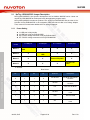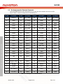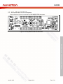
1
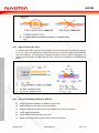
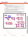
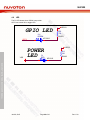
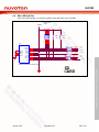
NUC505 ARM Cortex® -M 32-bit Microcontroller NuMicro™ Family NuTiny-SDK-NUC505 User Manual Nuvoton is providing this document only for reference purposes of NuMicro microcontroller based system design. Nuvoton assumes no responsibility for errors or omissions. All data and specifications are subject to change without notice. For additional information or questions, please contact: Nuvoton Technology Corporation. www.nuvoton.com Jan 08, 2015 Page 1 of 26 Rev 1.00 NUMICRO™ NUTINY-SDK-NUC505 USER MANUAL The information described in this document is the exclusive intellectual property of Nuvoton Technology Corporation and shall not be reproduced without permission from Nuvoton. NUC505 Table of Contents 1 OVERVIEW ......................................................................................... 4 2 NUTINY-SDK-NUC505 INTRODUCTION...................................................... 5 NuTiny -SDK-NUC505 Jumper Description ....................................................... 6 2.1 2.1.1 Power Setting.................................................................................................... 6 2.1.2 Debug Connector ............................................................................................... 7 2.1.3 ICE USB Connector ............................................................................................ 7 2.1.4 USB Host Connector ........................................................................................... 7 2.1.5 USB High Device Connector .................................................................................. 7 2.1.6 Extended Connector ........................................................................................... 7 2.1.7 Reset Button ..................................................................................................... 7 2.1.8 RTC wakeup Button ............................................................................................ 7 2.1.9 Headphone ...................................................................................................... 7 2.1.10 Line................................................................................................................ 7 2.1.11 Power Connector ............................................................................................... 7 2.2 Pin Assignment for Extended Connector .......................................................... 8 2.3 NuTiny-SDK-NUC505 PCB Placemen ............................................................. 9 NUMICRO™ NUTINY-SDK-NUC505 USER MANUAL How to Start NuTiny -SDK-NUC505 on the Keil μVision® IDE ............................ 10 3 3.1 Keil uVision® IDE Software Download and Install ...............................................10 3.2 Nuvoton Nu-Link Driver Download and Install ...................................................10 3.3 Hardware Setup .......................................................................................10 3.4 Smpl_NuTiny-NUC505 Example Program........................................................11 NuTiny-EVB-NUC505 Schematic.............................................................. 13 4 4.1 NUC505 ................................................................................................13 4.2 RESET and RTC_WAKEUP Button ...............................................................14 4.3 Crystal ..................................................................................................14 4.3.1 HXT:High Speed Crystal(12 Mhz) .......................................................................... 14 4.3.2 LXT: Low Speed Crystal(32.768 Khz) ..................................................................... 14 4.4 ICE Interface ...........................................................................................15 4.5 Boot Select .............................................................................................16 4.6 USB 2.0 High Speed Device ........................................................................17 4.6.1 PCB Layer Stack-up .......................................................................................... 17 4.6.2 Through Hole for D+ and D- ................................................................................ 17 4.6.3 Signal Trace for D+ and D- .................................................................................. 18 Jan 08, 2015 Page 2 of 26 Rev 1.00 NUC505 Others PCB design guideline for USB 2.0- ............................................................... 18 4.6.4 5 4.7 Power ...................................................................................................19 4.8 LED .....................................................................................................20 4.9 Micro SDCard Slot ....................................................................................21 4.10 Audio Line In, Headphone out and MIC ..........................................................22 4.10.1 Audio Line In ................................................................................................... 22 4.10.2 Audio Headphone out ........................................................................................ 23 4.10.3 Audio Headphone out ........................................................................................ 24 REVISION HISTORY ............................................................................ 25 NUMICRO™ NUTINY-SDK-NUC505 USER MANUAL Jan 08, 2015 Page 3 of 26 Rev 1.00 NUC505 1 OVERVIEW NuTiny-SDK-NUC505 is the specific development tool for NuMicro NUC505 series. Users can use NuTiny-SDK-NUC505 to develop and verify the application program easily. NuTiny-SDK-NUC505 includes two portions. One is NuTiny-EVB-NUC505 and the other is NuLink-Me. NuTiny-EVB-NUC505 is the evaluation board and Nu-Link-Me is its Debug Adaptor. Thus, users do not need other additional ICE or debug equipment. ® ® The NuMicro NUC505 series 32-bit microcontrollers are embedded with ARM Cortex -M4F core for consumer and industrial applications which need high computing power and rich communication interfaces. ® ® The ARM Cortex -M4F core within NuMicro NUC505 series can run up to 100 MHz and support DSP extensions and Floating Point Unit (FPU) function. The NuMicro NUC505 series supports 128 Kbytes embedded SRAM with zero-wait state and 2 Mbytes embedded SPI Flash memory, and is equipped with plenty of high performance peripheral devices, such as 24-bit Audio CODEC, USB2.0 High-speed Device, USB2.0 Full-speed Host, and other peripheral. NUMICRO™ NUTINY-SDK-NUC505 USER MANUAL Jan 08, 2015 Page 4 of 26 Rev 1.00 NUC505 2 NUTINY-SDK-NUC505 INTRODUCTION NuTiny-SDK-NUC505 uses the NUC505Y013Y as the target microcontroller. Figure 2-1 is NuTiny-SDK-NUC505 for NUC505 series, the left portion is called NuTiny-EVB-NUC505 and the right portion is Debug Adaptor called Nu-Link-Me. NuTiny-EVB-NUC505 is similar to other development boards. Users can use it to develop and verify applications to emulate the real behavior. The on board chip covers NUC505 series features. The NuTiny-EVB-NUC505 can be a real system controller to design users’ target systems, supports usb high speed interface, audio headphone out, audio line in and sdcad slot. Nu-Link-Me is a Debug Adaptor. The Nu-Link-Me Debug Adaptor connects your PC's USB port to your target system (via Serial Wired Debug Port) and allows you to program and debug embedded programs on the target hardware. To use Nu-Link-Me Debug adaptor with IAR or Keil, please refer to “Nuvoton NuMicro™ IAR ICE driver user manual “or Nuvoton NuMicro™ Keil ICE driver user manual” in detail. These two documents will be stored in the local hard disk when the user installs each driver. NUMICRO™ NUTINY-SDK-NUC505 USER MANUAL Figure 2-1 NuTiny-SDK-NUC505 (PCB Board) Jan 08, 2015 Page 5 of 26 Rev 1.00 NUC505 2.1 NuTiny -SDK-NUC505 Jumper Description NuTiny-SDK-NUC505 is the specific development tool for NuMicro NUC505 series. Users can use NuTiny-SDK-NUC505 to develop and verify the application program easily. NuTiny-SDK-NUC505 includes two portions. One is NuTiny-EVB-NUC505 and the other is NuLink-Me. NuTiny-EVB-NUC505 is the evaluation board and Nu-Link-Me is its Debug Adaptor. Thus, users do not need other additional ICE or debug equipment. 2.1.1 Power Setting J1: USB port in Nu-Link-Me J2: USB port in NuTiny-EVB-NUC505 JP8: VCC33 Voltage connecter in NuTiny-EVB-NUC505 JP7: P5VCC Voltage connecter in NuTiny-EVB-NUC505 POWER model J1 USB port Model 1 Connect to PC USB J2 USB port JP7 P5VCC JP8 VCC33 X X X NUMICRO™ NUTINY-SDK-NUC505 USER MANUAL Model 2 X Connect to PC USB X X Model 3 X X External 5V power X Model 3 X X X External 3.3V power X: Unused. Boot Select S4 S3 S2 S1 BootFrom Descriptions 0 1 1 0 ICE SPI EXT ICE Mode with External SPI Flash 0 1 1 1 ICE-SPI ICE Mode with Internal SPI Flash 1 0 1 1 ICP Boot from ICP Mode 1 1 0 1 SPI EXT Boot from External SPI Flash 1 1 1 0 USB Boot from USB 1 1 1 1 SPI Boot from Internal SPI Flash Jan 08, 2015 Page 6 of 26 Rev 1.00 NUC505 2.1.2 Debug Connector JP4: Connector in target board (NuTiny-EVB-NUC505) for connecting with Nuvoton ICE adaptor (Nu-Link-Me) JP1: Connector in ICE adaptor (Nu-Link-Me) for connecting with a target board (for example NuTiny-EVB-NUC505) 2.1.3 ICE USB Connector J2: Mini USB Connector in Nu-Link-Me connected to a PC USB port 2.1.4 USB Host Connector CON3: USB A type Connector in NUC505 USB host function connected to USB device 2.1.5 USB High Device Connector J4: Mini USB Connector in NUC505 USB device high speed function connected to PC USB port (Note) using the USB high speed device need external stable power for JP7 2.1.6 Extended Connector JP3, JP4, JP5 and JP7: Show all chip pins in NuTiny-EVB-NUC505 Reset Button NUMICRO™ NUTINY-SDK-NUC505 USER MANUAL 2.1.7 SW2: Reset button in NuTiny-EVB-NUC505 2.1.8 RTC wakeup Button SW3: RTC wakeup button in NuTiny-EVB-NUC505 2.1.9 Headphone CON2: NUC505 audio headphones connect. 2.1.10 Line CON1: NUC505 audio line in connect. 2.1.11 Power Connector JP7: 5 VCC connector in NuTiny-EVB-NUC505 JP8: 3.3 VCC connector in NuTiny-EVB-NUC505 JP9: GND connector in NuTiny-EVB-NUC505 Jan 08, 2015 Page 7 of 26 Rev 1.00 NUC505 2.2 Pin Assignment for Extended Connector NuTiny-EVB-NUC505 provides NUC505YO13Y on board and the extended connector for QFN88 pin. Table 2-1 is the pin assignment for NUC505YO13Y NUMICRO™ NUTINY-SDK-NUC505 USER MANUAL Pin No Pin Name Pin No Pin Name Pin No Pin Name Pin No Pin Name 01 RESETn 23 RTC_VDD33 45 GPB5 67 SAR_VDD33 02 GPD0 24 RTC_RPWR 46 GPB5 68 SAR_VSS33 03 GPD1 25 RTC_RWAKEn 47 GPB6 69 GPA0 04 GPB13 26 RTX_XIN 48 GPB7 70 GPA1 05 GPB14 27 RTC_XOUT 49 UD_CDET 71 GPA2 06 GPB15 28 GPA8 50 GPB8 72 GPA3 07 GPB15 29 GPA9 51 GPB9 73 GPA4 08 GPC1 30 GPA10 52 VDD33 74 GPA5 09 GPC2 31 GPA11 53 HP_VDD33 75 GPA6 10 VDD33 32 GPA12 54 LHP_OUT 76 GPA7 11 GPC3 33 GPA13 55 VCMBF 77 VDD12 12 GPC4 34 GPA14 56 RHP_OUT 78 GPB10 13 GPC5 35 GPA15 57 HP_VSS33 79 GPB11 14 GPC6 36 GPC7 58 VMID 80 GPB12 15 VDD12 37 GPC8 59 AVDD33 81 VDD33 16 XIN 38 GPC9 60 MIC1P 82 GPC11 17 XOUT 39 GPC10 61 MIC1N 83 GPC12 18 PLL_UD_VDD12 40 VDD33 62 LLINEIN/MICBIAS 84 GPC13 19 UD_DM 41 GPB0 63 VDD12 85 GPC14 20 UD_DP 42 GPB1 64 GPD2 86 AVDD 21 UD_VDD33 43 GPB2 65 GPD3 87 VOUT 22 UD_REXT 44 GPB3 66 GPD4 88 AGND Table 2-1 Pin Assignment for NUC505YO13Y Jan 08, 2015 Page 8 of 26 Rev 1.00 NUC505 2.3 NuTiny-SDK-NUC505 PCB Placemen Users can refer to Figure 2-2 for the NuTiny-SDK-NUC505 PCB placements. Figure 2-2 NuTiny-SDK-NUC505 PCB Placement NUMICRO™ NUTINY-SDK-NUC505 USER MANUAL Jan 08, 2015 Page 9 of 26 Rev 1.00 NUC505 3 HOW TO START NUTINY -SDK-NUC505 ON THE KEIL ΜVISION® IDE Keil uVision® IDE Software Download and Install 3.1 ® Please visit the Keil company website (http://www.keil.com) to download the Keil μVision IDE and install the RVMDK 3.2 Nuvoton Nu-Link Driver Download and Install ™ Please visit the Nuvoton company NuMicro website (http://www.nuvoton.com/NuMicro ) to ™ ® download “NuMicro Keil μVision IDE driver” file. When the Nu-Link driver has been well downloaded, please unzip the file and execute the “Nu-Link_Keil_Driver.exe” to install the driver. 3.3 Hardware Setup The hardware setup is shown as Figure 3-1 NUMICRO™ NUTINY-SDK-NUC505 USER MANUAL Figure 3-1 NuTiny-SDK-NUC505 Hardware Setup Boot form ICE-SPI mode to select ICE Mode with Internal SPI Flash S4 S3 S2 S1 0 1 1 0 ICE SPI EXT ICE Mode with External SPI Flash 0 1 1 1 ICE-SPI ICE Mode with Internal SPI Flash 1 0 1 1 ICP Boot from ICP Mode 1 1 0 1 SPI EXT Boot from External SPI Flash 1 1 1 0 USB Boot from USB Jan 08, 2015 Boot From Page 10 of 26 Descriptions Rev 1.00 NUC505 1 3.4 1 1 1 SPI Boot from Internal SPI Flash Smpl_NuTiny-NUC505 Example Program This example demonstrates the ease of downloading and debugging an application on a NuTinySDK-NUC505 board. It can be found on Figure 3-2 list directory and downloaded from Nuvoton ™ NuMicro website. Directory Project File To use this example: The LED will toggle on the NuTiny-EVB-NUC505 board. Start μVision® Project-Open Open the Smpl_NuTiny.uvproj project file Project - Build Compile and link the Smpl_NuTiny application Jan 08, 2015 Start debug mode Using the debugger commands, you may: Review variables in the watch window Single step through code Page 11 of 26 Rev 1.00 NUMICRO™ NUTINY-SDK-NUC505 USER MANUAL Figure 3-2 Smpl_NuTiny_NUC505 Example Directory NUC505 Flash – Download Program the application code into onchip Flash ROM Reset the device Run the application NUMICRO™ NUTINY-SDK-NUC505 USER MANUAL Jan 08, 2015 Page 12 of 26 Rev 1.00 P23 P24 P25 P26 P27 P28 P29 P30 P31 P32 P33 P34 P35 P36 P37 P38 P39 P40 P41 P42 P43 P44 RTC_VDD33 RTC_RPWR RTC_RWAKEn RTC_XIN RTC_XOUT GPA8 GPA9 GPA10 GPA11 GPA12 GPA13 GPA14 GPA15 GPC7 GPC8 GPC9 GPC10 VDD33 GPB0 GPB1 GPB2 GPB3 U2 VSS RESETn GPD0 ICECLK GPD1 ICEDAT GPB13 GPB14 GPB15 GPC0 GPC1 GPC2 VDD33 GPC3 GPC4 GPC5 GPC6 VDD12 XIN XOUT PLL_UD_VDD12 UD_DM UD_DP UD_VDD33 UD_REXT 1 2 3 4 5 6 7 8 9 10 11 12 13 14 15 16 17 18 19 20 21 22 R22 12.1K VSS MUST_KEEP_IT NUC505_QFN88 LDO_AVSS LDO_VOUT12 LDO_AVDD GPC14 GPC13 GPC12 GPC11 VDD33 GPB12 GPB11 GPB10 VDD12 GPA7 GPA6 GPA5 GPA4 GPA3 GPA2 GPA1 GPA0 SAR_VSS SAR_VDD33 P88 P87 P86 P85 P84 P83 P82 P81 P80 P79 P78 P77 P76 P75 P74 P73 P72 P71 P70 P69 P68 P67 MUST_KEEP_IT RESETn GPD[0]/ICE_CLK/SCL0 GPD[1]/ICE_DAT/SDA0 GPB[13]/SPI2_DI/UHC_DM1/RTS2/PWM[3] GPB[14]/SCL1/UHC_DP1 GPB15/SDA1/UHC_DM1 GPC[0]/SD_CMD GPC[1]/SD_CLK GPC[2]/SD_CDn VDD33_L GPC[3] GPC[4]/SD_DAT[0] GPC[5]/SD_DAT[1] GPC[6]/SD_DAT[2] VDD12 XIN XOUT PLL_UD_VDD12 UD_DM UD_DP UD_VDD33 UD_REXT GPD[4]/RLINEIN GPD[3]/MIC2N GPD[2]/MIC2P ADAC_VDD12 MICBIAS/LLINEIN MIC1N MIC1P ADCA_VDD33 VMID ADAC_HPVSS33 RHPOUT VCMBF LHPOUT ADAC_HPVDD33 VDD33 GPB[9]/SD_DAT[3]/OV_FLAG/RTS1/ETMG1_CAP GPB[8]/SD_DAT[2]/USB_PWEN/CTS1/ETMR1_TGL UD_CDET GPB[7]/SD_DAT[1]/RXD1 GPB[6]/SD_DAT[0]/TXD1 GPB[5]/SPI1_DI/SD_CDn GPB[4]/SPI1_DO/SY SCFG[3] Page 13 of 26 66 65 64 63 62 61 60 59 58 57 56 55 54 53 52 51 50 49 48 47 46 45 GPD4 GPD3 GPD2 ADAC_VDD12 MICBIAS MIC1N MIC1P ADAC_VDD33 VMID ADAC_VSS RHPOUT VCMBF LHPOUT ADAC_HPVDD33 VDD33 GPB9 GPB8 UD_CDET GPB7 GPB6 GPB5 GPB4 P66 P65 P64 P63 P62 P61 P60 P59 P58 P57 P56 P55 P54 P53 P52 P51 P50 P49 P48 P47 P46 P45 C9 0.01u MUST_KEEP_IT MCU Rev 1.00 NUMICRO™ NUTINY-SDK-NUC505 USER MANUAL Jan 08, 2015 P1 P2 P3 P4 P5 P6 P7 P8 P9 P10 P11 P12 P13 P14 P15 P16 P17 P18 P19 P20 P21 P22 88 87 86 85 84 83 82 81 80 79 78 77 76 75 74 73 72 71 70 69 68 67 AVSS QFN with Exposed Pad LDO_AVSS LDO_VOUT12 LDO_AVDD GPC[14]/UHC_DM0 GPC[13]/UHC_DP0 GPC[12]/I2S_BCLK/PWM[3]/ETMR3_CAP GPC[11]/I2S_LRCLK/PWM[2]/ETMR3_TGL VDD33_T GPB[12]/SPI2_DO/UHC_DP1/CTS2/PWM[2] GPB[11]/SPI2_CLK/SDA1/RXD2/PWM[1] GPB[10]/SPI2_CS0n/SCL1/TXD2/PWM[0] VDD12 GPA[7]/ADC[7] GPA[6]/ADC[6] GPA[5]/ADC[5] GPA[4]/ADC[4]/IS2_DATAO GPA[3]/ADC[3]/I2S_DATAI/DMIC_DAT GPA[2]/ADC[2]/I2S_MCLK/DMIC_CLK GPA[1]/ADC[1] GPA[0]/ADC[0] SAR_VSS33 SAR_VDD33 C6 10uF/10V RTC_VDD33 RTC_RPWR RTC_RWAKEn RTC_XIN RTC_XOUT GPA[8]/SPI0_CS0n/I2S_LRCLK/TXD1 GPA[9]/SPI0_CLK/I2S_BCLK/RXD1/SYSCFG[0] GPA[10]/SPI0_DO/SD_CLK/SCL1/SYSCFG[1] GPA[11]/SPI0_DI/SD_CMD/SDA1 GPA[12]/SPI0_D2/ETMR0_TGL GPA[13]/SPI0_D3/SD_CDn/ETMR0_CAP GPA[14]/SD_DAT[0]/SCL0 GPA[15]/SD_DAT[1]/SDA0 GPC[7]/SD_DAT[3] GPC[8]/I2S_MCLK GPC[9]/I2S_DATAI/PWM[0]/ETMR2_TGL GPC[10]/I2S_DATAO/PWM[1]/ETMR2_CAP VDD33 GPB[0]/SD_DAT[2]/SCL0/TXD0 GPB[1]/SD_DAT[3]/SDA0/RXD0 GPB[2]/SPI1_CS0n/SD_CMD GPB[3]/SPI1_CLK/SD_CLK/SYSCFG[2] 4.1 89 4 23 24 25 26 27 28 29 30 31 32 33 34 35 36 37 38 39 40 41 42 43 44 EPAD NUC505 NUTINY-EVB-NUC505 SCHEMATIC NUC505 AVDD33 C5 0.1U C0603 TANT-A + CP2 10u ADAC_VSS NUC505 4.2 RESET and RTC_WAKEUP Button The reset need R 10k and C 10uf for reset circuit. VDD33 Reset VDD33 R37 10K R0603 SW2 PUSH BOTTOM SW R40 10K R0603 SW3 PUSH BOTTOM SW RESETn RTC_RWAKEn RTC WAKEUP C23 10uF/10V TANT-A VSS VSS 4.3 VSS Crystal NUMICRO™ NUTINY-SDK-NUC505 USER MANUAL 4.3.1 HXT:High Speed Crystal(12 Mhz) For C24 and C25 is recommended to use high-quality ceramic capacitors in the 5pF~20pF range, designed for high-frequency applications and selected to meet the requirements of the crystal or resonator. C24 and C25 are usually the same value. The crystal manufacturer typically specifies a load capacitance that is the series combination of C24 and C25. The PCB and MCU pin capacitances must be included when sizing C24 and C25 (20pF can be used as a rough estimation of the combined pin and board capacitance), external resister need 1 MHz 4.3.2 LXT: Low Speed Crystal(32.768 Khz) For C21 and C22 is recommended to use high-quality ceramic capacitors in the 5~33 pF range, designed for RTC applications and selected to meet the requirements of the crystal or resonator, external resister need 10Mhz Applications requiring oscillators on NUC505 series MCUs must take PCB layout into consideration. The oscillators on NUC505 series MCUs consume very little current, and it sometimes makes the oscillator circuit sensitive to neighboring circuits. The following lists some PCB design guidelines: Jan 08, 2015 Page 14 of 26 Rev 1.00 NUC505 C21 33p C24 20p RTC_XIN XIN C0603 C0603 C25 20p X3 12MHz XTAL3-1 C0603 VSS 4.4 R38 1M R0603 XOUT C22 33p X2 32.768K XTAL-3.4MM-2P R36 10M R0603 RTC_XOUT C0603 12Mhz Crystal VSS 32.768Khz Crystal for RTC ICE Interface For ICE Mode debug or ICP Mode download code to flash ICEVCC_T JP4 M0_TXD M0_RXD 2 4 6 8 10 VDD33 ICEDAT ICECLK RESETn NUMICRO™ NUTINY-SDK-NUC505 USER MANUAL GPB0 GPB1 1 3 5 7 9 NC VSS ICE INTERFACE Jan 08, 2015 Page 15 of 26 Rev 1.00 NUC505 4.5 Boot Select The power-on setting is used to configure the chip to enter the specified state when the chip is powered up or reset. Since each pin of power on setting has an internal pulled-up resistor when in reset period. If the application needs to set the configuration to “0”, the proper pull-down resistor of 10KOhm must be added for the corresponding configuration pins. S3 1 1 0 1 1 1 S2 1 1 1 0 1 1 S1 0 1 1 1 0 1 R0603 R0603 R0603 R0603 Boot Fm IC E-SPIext IC E-SPI IC P SPIext USB SPI NUMICRO™ NUTINY-SDK-NUC505 USER MANUAL BOOT SELECT Jan 08, 2015 Page 16 of 26 S4 S3 S2 S1 10K 10K 10K 10K ON S4 0 0 1 1 1 1 R28 R29 R30 R31 1 1 2 3 4 GPA9 GPA10 GPB3 GPB4 SW1 HPS604-E 0 VSS Rev 1.00 NUC505 4.6 USB 2.0 High Speed Device The layout rule needs to take USB 2.0 high speed device. R33 20K R32 39K R0603 DVBUS R0603 USB Device UD_CDET R34 2.2 J2 mini USB 5pin R0603 UD_DM UD_DP DM1 DP1 R35 2.2 R0603 L6 1 2 3 4 5 VCC DM DP NC GND SHIELD SHIELD SHIELD SHIELD 6 7 8 9 USB_MINI_B 4.6.1 USBT_VSS PCB Layer Stack-up For a USB 2.0 high-speed design, recommend to use at least a four-layer PCB for best signal characteristics. The majority of signal traces should run on a single layer, next to this layer should be the GND plane, which is solid with no cuts. Avoid running signal traces across a split in the ground or power plane. Minimizing the number of signal vias reduces EMI by reducing inductance at high frequencies. If you attempt a two-layer board, you will need to reduce the thickness of the PCB along with increasing separation of traces and increased trace widths to maintain the impedance match of the D+ and D- data lines. To put things in perspective, what would be D+ and D- lines at 6mil trace and 6mil space in a four layer board become 18mils wide with 8mil spacing in a two-layer board. 4.6.2 Through Hole for D+ and D- For the two-layer or multi-layer of PCB, when the signals of D+ and D- need to be through another layer, in which the resistively of through hole should be concerned. To lower the resistively issue for the sensitivity case, the two-via or multi-via should be adapted, as shown in the following figure. Jan 08, 2015 Page 17 of 26 Rev 1.00 NUMICRO™ NUTINY-SDK-NUC505 USER MANUAL L0805 VSS NUC505 4.6.3 Signal Trace for D+ and D- To avoid the trace effect signal for the eye diagram, the trace length should be almost the same of D+ and D-. Then, the characteristic impedance should be a symmetrical path for the differential end of the USB port. The characteristic impedance should be 90 for USB 2.0 high speed. For reducing the trace length, the USB terminal should be as close as the USB port of NUC505 series MCUs. NUMICRO™ NUTINY-SDK-NUC505 USER MANUAL 4.6.4 Others PCB design guideline for USB 2.0- Control differential impedance on USB traces (90 Ohms) Isolate USB traces from other circuitry and signals Keep bulk capacitors for down-stream port’s VBUS power close to connectors Isolate crystal and oscillator Isolate VRES resistor and keep short traces Bypass capacitors placed on bottom side to reduce board space Jan 08, 2015 Page 18 of 26 Rev 1.00 NUC505 4.7 Power The ADAC_VDD33, ADAC_HPVDD33, RTC_VDD33 need stable power in user application, 0 ohm can direct short in user application. The VDD pins must be connected to 3.3V with external decoupling capacitors. (a 0.1uF capacitor for each VDD pin and a 1uF capacitor for the whole chip). The AVDD pin recommend be connected to two external decoupling capacitors (0.1uF+10nF). To keep the analog power stable, additional precautions need to be taken to filter analog noise. The following are two suggestions for the board level designing: AVDD can be connected to VDD through a ferrite bead. The RTC _VDD33 pin also powers the RTC unit, allowing the RTC to operate even when the main digital supply (VDD) is turned off. If no external battery is used in the application, it is highly recommended to connect VBAT pin to VDD with a 0.1uF external decoupling capacitor. R14 0 LDO_VOUT12 POWER RB060L OUT R0603 VDD33 4 IN GND OUT PD1 SS24A 5VCC 1 2 3 1 2 DVBUS VDD12 UP1 RT9164A-3.3v CI9 0.1U C0603 R19 C29 0.1U C0603 0 SAR_VSS 0 LDO_AVSS R0603 CP3 10uF/10V R20 R0603 TANT-A AVSS 0 ADAC_VSS R0603 VSS AVDD33 R61 VSS R25 VDD33 SAR_VDD33 0 0 UD_VDD33 R0603 R0603 R10 R6 AU_VDD33 0 ADAC_VDD33 0 ADAC_HPVDD33 0 RTC_VDD33 R0603 R0603 R7 R0603 L4 VDD33 C18 0.1U C0603 L0603 C17 10uF/10V TANT-A L5 VSS AVDD33 C19 C0603 0.1U C20 10uF/10V TANT-A L0603 AVSS Note:The 0 ohm resister can short in user application. Jan 08, 2015 Page 19 of 26 Rev 1.00 NUMICRO™ NUTINY-SDK-NUC505 USER MANUAL R23 NUC505 4.8 LED The P1 LED shows when VDD33 has provider. GPC3 can control IO1 to toggle LED GPIO LED GPC3 VSS 2 IO1 GREEN 1 KP-2012 POWER LED RI0 330 R0603 VDD33 RI2 330 P1 RED 2 VDD33 R0603 1 KP-2012 NUMICRO™ NUTINY-SDK-NUC505 USER MANUAL Jan 08, 2015 Page 20 of 26 Rev 1.00 NUC505 4.9 Micro SDCard Slot U6 is micro SD Card Slot, it is access by SHDC mode, Max clock can run 50 Mhz 8 P 4 R-4 7 K RP 2 8 7 6 5 VDD33 R49 47k 47k 1 2 3 4 R48 U6 13 12 11 10 GND GND GND GND VSS DAT2 DAT3 CMD VDD CLK VSS DAT0 DAT1 CD 1 2 3 4 5 6 7 8 9 33 33 33 GPC6 GPC7 GPC0 (D2) (D3) (CMD) R58 33 GPC1 (CLK) R59 R60 R69 B8502A-13SB-HPA (T-Flash Card) 33 33 GPC4 GPC5 0 GPC2 (D0) (D1) (CDn) Page 21 of 26 NUMICRO™ NUTINY-SDK-NUC505 USER MANUAL SD CARD VSS Jan 08, 2015 R53 R54 R55 Rev 1.00 NUC505 4.10 Audio Line In, Headphone out and MIC For audio application, the headphone out for audio out, J7 is bais voltage select for MIC or line in. E-C Right channel F-D Left channel Audio F R8 0 GPD4 C7 1u ERLINEIN C8 220p ADAC_VSS LINE IN G CON1 B C E F D A R11 5K6 R16 8K2 MICBIAS_LINE_IN ELLINEIN D E CB3 0.1uF MICBIAS_MIC_IN + C12 220p R18 5K6 MICBIAS_LINE_IN MICBIAS MICBIAS_MIC_IN R15 2K2 ADAC_VSS C11 1uF 1-2 Short M1 G CON2 B C E F D A + LHPOUT + C15 100uF RHP LHP NUMICRO™ NUTINY-SDK-NUC505 USER MANUAL C16 100uF R26 47K CP1 4.7uF/10V R12 0 ADAC_VSS RHPOUT G PJK-634M PHONE-PJK-631 J7 1 2 3 A B R9 8K2 RLINEIN C10 1u C R27 47K R13 0 Headphone MIC R17 0 MIC1P + C13 220p - R21 0 MIC1N R24 2K2 C14 1uF PJK-634M PHONE-PJK-631 ADAC_VSS ADAC_VSS 4.10.1 Audio Line In The device provides left and right channel line-in inputs. The inputs are high impedance, low capacitance AC coupled. All inputs include independent PGA (programmable gain amplifier) and mute function. Passive RF and active Anti-Alias filters are also incorporated within the line inputs to prevent high frequencies aliasing into the audio band or otherwise degrading performance. The inputs are biased internally through the operational amplifier to Bais. The external components required to complete the line input application are shown in the following figure. Jan 08, 2015 Page 22 of 26 Rev 1.00 NUC505 R8 0 GPD4 C7 1u R9 8K2 RLINEIN LINE IN ERLINEIN C8 220p C10 1u G CON1 B C E F D A R11 5K6 ADAC_VSS R16 8K2 MICBIAS_LINE_IN ELLINEIN C12 220p R18 5K6 PJK-634M PHONE-PJK-631 R12 0 ADAC_VSS 4.10.2 Audio Headphone out The recommended external components are shown in the figure below: G CON2 B C E F D A LHPOUT + RHPOUT RHP + C15 100uF LHP C16 100uF R26 47K R27 47K R13 0 Headphone ADAC_VSS Jan 08, 2015 PJK-634M PHONE-PJK-631 Page 23 of 26 Rev 1.00 NUMICRO™ NUTINY-SDK-NUC505 USER MANUAL This device provides two low impedance line outputs (LHPOUT and RHPOUT), suitable for driving typical line loads of impedance 10k and capacitance 50pF. NUC505 4.10.3 Audio Headphone out The device supports 2 types of Microphone inputs that can be either differential or singleended, The differential mode as shown below. CB3 0.1uF MICBIAS_MIC_IN + R15 2K2 CP1 4.7uF/10V ADAC_VSS C11 1uF M1 MIC R17 0 MIC1P + C13 220p - R21 0 MIC1N NUMICRO™ NUTINY-SDK-NUC505 USER MANUAL R24 2K2 C14 1uF ADAC_VSS Jan 08, 2015 Page 24 of 26 Rev 1.00 NUC505 5 REVISION HISTORY Date Revision Description 2015.02.08 1.00 1. Initially issued. NUMICRO™ NUTINY-SDK-NUC505 USER MANUAL Jan 08, 2015 Page 25 of 26 Rev 1.00 NUC505 NUMICRO™ NUTINY-SDK-NUC505 USER MANUAL Important Notice Nuvoton Products are neither intended nor warranted for usage in systems or equipment, any malfunction or failure of which may cause loss of human life, bodily injury or severe property damage. Such applications are deemed, “Insecure Usage”. Insecure usage includes, but is not limited to: equipment for surgical implementation, atomic energy control instruments, airplane or spaceship instruments, the control or operation of dynamic, brake or safety systems designed for vehicular use, traffic signal instruments, all types of safety devices, and other applications intended to support or sustain life. All Insecure Usage shall be made at customer’s risk, and in the event that third parties lay claims to Nuvoton as a result of customer’s Insecure Usage, customer shall indemnify the damages and liabilities thus incurred by Nuvoton. Jan 08, 2015 Page 26 of 26 Rev 1.00