1
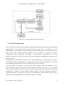
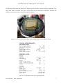
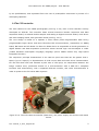
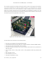
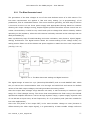
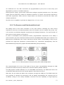
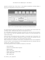
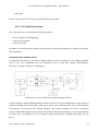
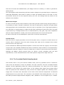
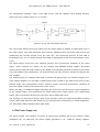
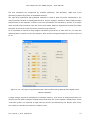
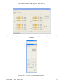
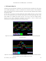
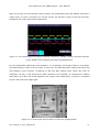
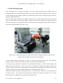
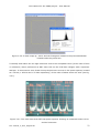
DIPARTIMENTO DI FISICA E ASTRONOMIA SEZIONE DI ASTRONOMIA CCD camera for the CAOS project - User Manual - M. Focardi(a) (a) Dipartimento di Fisica e Astronomia – Università di Firenze, L.go E. Fermi 2, 50125 Firenze, Italy Technical Report TR02-2011 Version 1.0 First issue (v. 1.0): June 2010 Final release (v. 1.0): August 2011 Dipartimento di Fisica e Astronomia – Sezione di Astronomia L.go E. Fermi 2, 50125 Firenze (Italy) Ph.+39 (055) 205 5200 CCD camera for the CAOS project – User Manual SUMMARY ABOUT THIS MANUAL ................................................................................................................... 4 1. THE CAOS PROJECT ................................................................................................................ 5 2. CCD CAMERA MAIN FEATURES .......................................................................................... 5 2.1. The CCD camera head .......................................................................... 6 2.1.1 The preamplifier board ........................................................................... 8 2.2 The CCD controller ............................................................................... 9 2.2.1 The Bias Generator board .................................................................... 11 2.2.2 The Sequencer and Data Acquisition board ............................................ 12 2.2.3 The Clock Driver board ........................................................................ 14 2.2.4 The Correlated Double Sampling board .................................................. 15 3 2.3 The Power Supply unit ........................................................................ 16 2.4 The high-level software interface and the acquisition SW ......................... 17 TESTS AND RESULTS ........................................................................................................... 20 3.2 AOC laboratory tests ........................................................................... 22 3.3 Spectrograph accommodation and tests ................................................ 24 4 CONCLUSIONS ........................................................................................................................ 24 5 REFERENCES........................................................................................................................... 25 6. APPENDIX A – Boards Schematics ......................................................................................... 26 7. APPENDIX B – Documentation CD ROM ............................................................................... 26 Ref.: Manual_2_2010_English.doc 2 CCD camera for the CAOS project – User Manual Ref.: Manual_2_2010_English.doc 3 CCD camera for the CAOS project – User Manual ABOUT THIS MANUAL This Manual concerns the image acquisition system developed for the focal plane of the CAOS (Catania Astrophysical Observatory Spectrograph) echelle spectrograph at Catania Astrophysical Observatory, located at Serra La Nave (CT, Italy). The system is based on a CCD camera whose performances and characteristics rely on a new controller entirely developed at the XUVLab of the Department of Physics and Astronomy of the University of Florence. Here are described the CCD camera head and controller characteristics as well as the innovative sequencer board based on FPGA programmable logic and the first tests and results performed at the XUVLab and OAC facilities. Keywords: CCD cameras, FPGAs, high resolution spectrograph, spectropolarimetry. Ref.: Manual_2_2010_English.doc 4 CCD camera for the CAOS project – User Manual 1. THE CAOS PROJECT The present observational activity at the OAC 91 cm Cassegrain telescope rely on the importance of the CAOS instrument, a higher resolution spectrograph with spectropolarimetry capability for the measure of stellar magnetic fields, doppler imaging of active stars and binary systems and stellar atmosphere studies [1]. CAOS is in fact an efficient, high-resolution, fiber-fed optical spectrograph with high stability and complete spectral coverage in one exposure. Its main characteristics are summarized in the following items: – spectral region of interest: 388–725 nm – spectral resolution: HR (R = 30000−45000−60000) and LR (R = 3000) – integral light mode or polarimetric mode – efficiency (integral light mode): > 20% – low scattered light With CAOS spectrograph it will be also possible to search for extra-solar planet systems, to perform asteroseismology measurements (i.e. amplitude and frequencies of stellar oscillations), long-term monitoring of hydrodynamic phenomena in hot stellar atmospheres and observations of diffuse clouds in the interstellar medium. Thanks to the CAOS CCD camera it will be possible to record digital images to be subsequently processes for understanding all the physical phenomena related to stellar and interstellar medium spectropolarimetry. 2. CCD CAMERA MAIN FEATURES The camera (see Fig. 2.a for a scheme) is mainly composed by three parts: ü the CAMERA HEAD, including the dewar with the cold finger, the CCD sensor, the shutter and the detector proximity electronics (preamplifier) located inside the dewar; ü the CONTROLLER, including the integrated sequencer and data acquisition board (SDAQ), the ADC and the correlated double sampling (CDS) circuit, the clock driver (CD) and the bias generator (BG) boards; ü the external POWER SUPPLY UNIT. Hereafter are described all the parts in their details. Ref.: Manual_2_2010_English.doc 5 CCD camera for the CAOS project – User Manual Figure 2.a. The CCD camera’s overall scheme. 2.1. The CCD camera head The CCD camera is based on the E2V-4240 AIMO (Advanced Inverted Mode) back-illuminated 2048x2048, 13.5 um square pixels, full-frame area device (see Fig. 2.1.a and Tab. 2.1.a for specifications). The advanced inverted mode operation (AIMO) gives a 100-times reduction in dark current with minimal full-well reduction and is suitable for use also at Peltier temperatures. Back illumination technology, in combination with extremely low noise amplifiers, makes the device well suited to the most demanding applications requiring a high dynamic range. The detector has two outputs, which can be used simultaneously to readout the two sensor halves and to reduce the readout time. CAOS design uses only the left amplifier even though the preamplifier board allows to mount electronics for both the outputs. The CCD imager is mounted in a non-hermetic metal package with the possibility to use a glass protection window and hosted inside an Oxford LN2 dewar (see Fig. 2.1.b), that hosts also the CCD preamplifier board. CCD is in contact with a cold finger cooled down from room temperature by means of liquid nitrogen filling the dewar. The CCD operating temperature (153K<Top<323K) is preserved by means of a temperature probe (PT100) and a heater, monitored and activated thanks to a Lakeshore external controller. Ref.: Manual_2_2010_English.doc 6 CCD camera for the CAOS project – User Manual The window that seals the dewar is a simple quartz window, without dioptric capability. The large area CCD (27,6x27,6 mm) cover a large field on the telescope focal plane, allowing the imaging of spectra of many stellar and diffuse objects. Figure 2.1.a. E2V-4240 CCD large area detector and its preamplifier board. Tab. 2.1.a. E2V-4240 CCD device specifications. Ref.: Manual_2_2010_English.doc 7 CCD camera for the CAOS project – User Manual Figure 2.1.b. The LN2 dewar with the shutter and optics to take test images. Initially the camera head and controller were placed on a optical bench at the OAC optical and electronics laboratory, where were performed focusing optimization procedures and calibrations before matching the CAOS spectrograph located at Serra La Nave, on Mt. Etna volcano slopes. 2.1.1 The preamplifier board The preamplifier board was originally designed to fit the existing circular mount bracket with a wedge cold finger (see Fig. 2.1.a) for matching the optical CAOS design requirements. It hosts a dual symmetrical preamplifier able to readout the left and right CCD outputs at the same time or, in alternative, to choose either. As known from literature, the correct design of this circuit is fundamental because the CCD signal might be highly affected by noise. In fact, in order to avoid video-signal degradations, it is necessary to amplify it before introducing any unwanted additional noise contribution. For this reason the preamplifier must be ultra-low-noise electronics. The preamp design is based on the AD797 operational amplifier. The AD797 is a very low noise, low distortion opamp. The low noise of 0.9 nV/√Hz, the excellent slew-rate of 20 V/µs and the low total harmonic distortion from audio to video bandwidths give the AD797 the wide dynamic range necessary for use as a preamplifier. The preamplifier board host also some R-C filter for CCD biasing and clocks filtering. The CCD output stage is connected to ground by means of a constant current driver load as requested Ref.: Manual_2_2010_English.doc 8 CCD camera for the CAOS project – User Manual by its specifications, and separated from the rest of preamplifier electronics by means of a decoupling capacitor. 2.2 The CCD controller The CCD camera for the CAOS spectrograph (see Fig. 2.2.a) uses a CCD controller entirely developed at XUVLab. The controller hosts several electronic boards: sequencer and data acquisition board, correlated double sampler and analog to digital converter board, clock driver and wave shaping board, bias generator board (see Fig. 2.2.b). The core design is based on a Spartan 3 Xilinx FPGA (Field Programmable Gate Array) programmable logics device and three Microchip PIC microcontrollers, respectively on SDAQ board, BG board and CD board. In facts the FPGA device is responsible to clocks generation in digital domain and data acquisition procedure whose internal logic was developed in VHDL (VHSIC Hardware Description Language) language (where VHSIC means Very High Speed Integrated Circuits). The sequencer principal characteristic is its read-out pixel rate that can be greater than 1 Mpix/s (up to 5 Mpix/s) in dependencies of CCD current load and clock driver characteristics. For the E2V-4240 CCD was selected a pixel rate of 150 kpx/s, as compromise between the image readout time, performed thanks to a microcontroller with a USB V2.0 compliant interface and, alternatively, with a separate Ethernet module, and noise characteristics in order to preserve the full 16 bit ADC dynamic. Figure 2.2.a. The CCD camera controller (black box), the power supply unit and the CCD hosts dewar. Ref.: Manual_2_2010_English.doc 9 CCD camera for the CAOS project – User Manual The controller hosts all the necessary electronics board to acquire new images and to perform every action demanded by the high-level software interface. It is characterized by a modular architecture (see Fig. 2.2.b). This contributes to a larger versatility, because every electronic board can be easily removed from the bus backplane and substituted by another one. This feature brings several benefits since the laboratory prototype needs to perform a fine tuning of all boards to get the best optimisation of the camera. Figure 2.2.b. The CCD camera controller and its electronics boards. Its main features are summarize in the following items: ü Pixel rate up to 5 Mpixel/s (from lab performed tests) ü Commands and data I/O through USB V2.0 compliant interface or Ethernet XPORT module ü CCD timing fully SW programmable (VHDL language) ü Automatic acquisition procedures with various exposure times and free-run procedures to clean the sensor ü Up to 8 clocks (-18V to +18V), 8 bias (-15V to +32V) available to allow easy interface with CCDs ü ADC conversion: 16 bit ü Time resolution up to 10 ns ü Low power consumption (<5 W) Ref.: Manual_2_2010_English.doc 10 CCD camera for the CAOS project – User Manual 2.2.1 The Bias Generator board The generation of the bias voltages is one of the most delicate issues of a CCD camera. The low-noise requirements are against a fast and easy setting (or re-programming) of all parameters, that is a desirable feature. This occurs because generally, the best way to achieve a low-noise circuit is to use linear power supply with appropriate filtering based on resistors allowing the output voltages tuning, despite digital systems that allow remote control but are noisier. Nevertheless, it could be very useful and quick to change bias values remotely without operating on the hardware, when the CCD camera is already mounted at the telescope and not easily accessible [2]. After a preliminary step of bread-boarding and noise evaluation, was chosen a hybrid (digitalanalog) architecture. The digital section allows the remote setting of the voltage levels; the analog section filters out all the biases and power supplies to match the low-noise requirement (see Fig. 2.2.1.a). Figure 2.2.1.a. The Bias Generator analog and digital sections. The digital design is based on a µC (Microchip PIC16F877) and an octal MAX547 DAC. While the µC ensures the communication with a PC through an RS232 link and stores the default values of the DAC output voltages, the DAC generates the setting values. Since the output DAC voltages range between ±4.096V, it was necessary to introduce a gain stage, for a final voltages tuning. The device that accomplishes this final tuning is the OP295 operational amplifier that have a rail-to-rail high dynamic range, a power supply rejection ratio of 110 dB and an input noise, at low frequencies, of 1.5 µV peak-to peak (and then suitable for low noise applications). Since the Vod (drain of the output FET) is the most sensitive voltage to noise (because it affects directly the video output signal), it is generated by a linear tunable voltage reference Ref.: Manual_2_2010_English.doc 11 CCD camera for the CAOS project – User Manual on a different line. The Vdd is therefore not programmable by GUI, but it is less noisy (and adjustable by means of variable resistors). Filtering power supply, ground and output bias voltages required particular care. The power supply lines are filtered by means of capacitive-inductive "Π" filters, the ground is filtered by some EMI suppression filters and the output biases are filtered by low-pass RC filters with multiple capacitors. The BG circuit is capable to generate 8 voltages from -15 V to +32 V. 2.2.2 The Sequencer and Data Acquisition board The SDAQ circuit is the main innovation of the CCD camera, matching the clock timing required for the CCD, the data acquisition and I/F functions (see for details TR3_2010). Fig. 2.2.2.a shows a schematic diagram representing the SDAQ architecture. The dual function of this circuit is clearly shown in the picture. In order to accomplish such operational modes, programmable components as an FPGA, a microcontroller (µC) and six banks of RAM memories (6x16Mbit Static RAM) were selected. The FPGA can be considered as the "heart" and the µC as the "brain" of the SDAQ; in fact, the µC performs the high-level operations (communication I/F, commands management) and the FPGA handles high frequency signals and data addressing and processing. Figure 2.2.2.a. Data acquisition and processing flow inside SDAQ board. The communication I/F is one of the tasks of the µC that is accomplished through one USB port and one Ethernet port by means of an external module (XPORT module). The DAQ system consists basically on a 12-MB SRAM controlled by the FPGA that stores the 16-bits ADC data and wait for the request signal to send them to the µC. After that, the µC sends the data to the computer, through the USB port. The FPGA keeps the core program to operate the Sequencer and its design accomplishes the required level of versatility. Owing to the widely available resources and the capability of high-frequency Ref.: Manual_2_2010_English.doc 12 CCD camera for the CAOS project – User Manual operation (100 MHz clock) of this device, it was possible to implement a modular design, a high level of configurability and a high time resolution. Figure 2.2.2.b. A schematic diagram representing the SDAQ architecture. The performed tests reported an USB transfer rate of 600 KBytes/s and a total transfer time (including a 2048 × 2048 tests image read-out at 300 kpixel/s) of 30 s. The configurability of parameters is presently not useful for the end users of the CCD camera, but is crucial for the tests and optimization phases; therefore, the camera parameters are "frozen" after testing. During the tests, two operational modes are available: a "test mode" and a "setup mode". The first mode allows the Sequencer generating the signals checking the electronics and the general functions of the camera, once a certain CCD has been selected. When the Sequencer is operated in "setup mode", the parameters for the end-user application are fixed. However, some parameters are still configurable also after the controller setup (as exposure time, windowing, pixel binning). The following parameters can be modified or selected if in "test mode": • Array dimensions • Continuous acquisition without exposure • Exposure time • Dark or bias image • Output selection (for buttable CCDs) • Clock voltage levels • Bias voltage levels Ref.: Manual_2_2010_English.doc 13 CCD camera for the CAOS project – User Manual • Pixel rate In the "setup mode" it can also be modified the clock timing. 2.2.3 The Clock Driver board The clock driver circuit performs the following tasks: • Clock voltage levels adjusting • Wave-form shaping • Current driving Hereafter are described the design choices and the hardware selections to achieve such tasks and operations. Adjusting clock voltage levels As discussed previously, the clock’s digital voltage levels generated by the SDAQ (typically 3.3V or 5V, TTL compatible) are not compliant with the CCD bias voltage specifications. Therefore, voltage regulation is mandatory. Figure 2.2.3.a. The Clock Driver hybrid design scheme. It was selected a hybrid (digital-analog) design to get a low-noise configurable circuit based on Digital to Analog Converters (DAC) (see Fig. 2.2.3.a). The selected device is the octal MAX547 converting a 13-bits input into analog voltages. The output voltages are fed to an analog switch (Maxim Max333A) that generates waveforms having time behaviour as the input signals (a clock from the SDAQ) and the required voltage amplitudes (voltages generated by the DAC). Ref.: Manual_2_2010_English.doc 14 CCD camera for the CAOS project – User Manual Since the CD hosts two MAX547 DAC (16 voltage levels are needed), it is able to generate 8 analog clocks. The input digital words determining the DAC output voltages are generated by an on-board µC (Microchip PIC16F877) that sends on power-on some pre-defined values to the DAC. If such pre-defined values are not the required values, the user can change them by means of the software user interface. Wave-form shaper In order to avoid too fast clock transitions, that could generate losses during charge transfer, it is necessary to make "smooth" transients. This can be achieved by using RC low-pass filters with appropriate time characteristics. Since the CCD is equivalent (as a rough approximation) to an RC load, it is good practice to match the RC filter impedance to that of the CCD. This task is performed by a voltage follower that is characterised by unity gain, high input impedance and low output impedance. Usually, this device performs also the current driving task. In order to limit the current absorption a pixel-rate of 150 kHz was selected. Current driver Since the CCD is roughly equivalent to an RC low-pass circuit, it requires a certain amount of current, that is maximum when the clocks change their state (as for example when transit from the low to the high level). It was selected the AD812 operational amplifier current driver that can supply a 50 mA output current and in the amplifier feedback loop where included a couple of BJTs in a complementary configuration that can supply a current up to 800 mA, in order to ensure the correct CCD drive. Although the AD812 cannot provide alone an electric current compliant with the CCD requirements, it was selected because of its wide dynamic range and its high slew rate. 2.2.4 The Correlated Double Sampling board CCD sensors have a very low intrinsic readout noise, thus any possible source of electronic noise must be reduced as much as possible. The A/D converter and the correlated double sampler circuits significantly affect the camera performances: the noise level of the signal processing is the camera key quality factor, so the analog video signal from preamp board must be preserved and shielded by noisy sources like digital signals and switching power supply lines. The same care was taken in the choice of the discrete components: all selected components are very low-noise. The converter is the AD7677 from Analog Devices: it is a 16 bits SAR (Successive Approximation Register) ADC, capable to convert signals up to 1 MSPS. Ref.: Manual_2_2010_English.doc 15 CCD camera for the CAOS project – User Manual The operational amplifier, used in the CDS circuit, was the AD8021 from Analog Devices, having an input voltage noise of 2.1 nV/Hz½. Figure 2.2.4.a. The CDS board scheme. The reset noise affects each pixel-readout at the output stage by adding an offset bias level to the video signal. The CDS eliminates this noise by sampling twice the pixel video signal and subtracting the second sample from the first one. The functional scheme of the CDS is illustrated in Fig. 2.2.4.a while the ADC-CDS PCB is highlighted as the first board shown in Fig. 2.2.b. The figure above shows how two switches perform the synchronous sampling of the video signal. Such switches are driven by the CLAMP and SAMPLE digital signals generated synchronously with the serial clocks by the SDAQ. The sampled signals are stored in the Clamp (CC) and Sample (CS) capacitance. CC performs also the sign inversion needed to subtract the two samples. The buffering and the "Sample and Hold" functions are achieved by two follower stages (lownoise opamp AD8021). In this CDS, a differential couple of FETs is put before the input of each follower stage. This configuration avoids "common mode" noise and temperature variations of the input signal, lowering the total noise of the circuit. Before the ADC, an additional stage decouples the converter input from the output impedance of the sample stage, and transforms the single-ended CDS output signal into a differential signal. This is necessary because the converter has a differential input. The heritage of CDS board design came from HiVeCam CDS and Herschel/SCORE sounding rocket visible light detector CDS board [3]-[7] that has flown successfully on 2009 September, 14th from White Sands Missile Range (NM, USA). 2.3 The Power Supply unit The power supply unit contains a number of commercial modules fed by the network supply (220V@50 Hz). In particular, the power supply generates ± 5V, ±18V for analog supplies, Ref.: Manual_2_2010_English.doc 16 CCD camera for the CAOS project – User Manual +24V for digital supplies and +32 V only for the Vod voltage. While ± 5V and ±18V supply directly the analog circuits and are generated by linear modules, the +24V, generated by an AC/DC switching module, supplies only the SDAQ, because it derives all the digital voltages from DC/DC converters requiring +24V as input bias. Additional linear voltages are +48V, +42V, +38V, +21V. Note that linear voltages are favoured when noise issues are critical, because switching modules work at a certain frequency that can affect the signals and the ground reference. The amount of the output power was estimated on the basis of calculations and previous experiences and was over-dimensioned: 24V @ 40W, ±5V @ 5W, ±18V @ 50W, 32V @ 48W. 2.4 The high-level software interface and the acquisition SW The high-level SW interface (see Fig. 2.4.a/b/c) has been developed under the freely available NOKIA Qt Creator that allow to develop open source software governed by the GNU General Public License (GPL). Qt Creator is a complete integrated development environment (IDE) for creating applications with the Qt application framework. Qt is designed for developing applications and user interfaces once and deploying them across several desktop and mobile operating systems. It includes: • An advanced C++ code editor • Integrated GUI layout and forms designer • Project and build management tools • Integrated, context-sensitive help system • Visual debugger • Rapid code navigation tools • Supports multiple platforms (WinXP, VISTA, Windows 7, Linux, Mac) The high-level SW interfaces with low-level SW (microcontrollers firmware - FW) by means of two distinct serial RS232 interfaces (CD and BG boards – see Fig. 2.4.a and Fig. 2.4.b) and a USB interface (SDAQ board – see Fig. 2.4.c). CD e BG microcontrollers are used to set digital values on DACs, decoding a precisely formatted command string. The microcontrollers implemented commands cover in practice all the possible tasks performed by a DAC and are able to full control CD and BG boards. To upload FW on microcontrollers by means of the RS232 interface, as for the USB interface, is it possible to use a bootloader, a simple firmware and graphical interface able to accelerate all the programming tasks. Ref.: Manual_2_2010_English.doc 17 CCD camera for the CAOS project – User Manual The SW interfaces are supported by multiple platforms, like Windows, UNIX and Linux operating systems by means of dedicated libraries. The high-level acquisition SW graphical interface is used to pass low-level commands to the microcontroller located on SDAQ board and to acquire images, thanks to VHDL DAQ firmware implemented in the Spartan 3 FPGA. Low-level commands are decoded by means of a simple 4x16 decoder that interfaces with the main Finite State Machine implemented inside the FPGA that acts as the brain of all sequencer and driving procedures. So it is possible to start and stop images acquisition procedures, to start free-run, to reset the data acquisition system, to set the exposure time and the image dimensions in pixels units and so on. Figure 2.4.a. The high-level Bias Generator SW interface with graphical bias digital levels setting capability. A single image requires 8.595 Kbytes of storage memory, a bit more of 8 Mbytes because we acquire also 50 blank elements located before and after the serial register’s 2048 pixels. These “overscan” pixels, not exposed to light sources and so not affected by the photon shot noise, are useful to evaluate the electronic readout noise. Ref.: Manual_2_2010_English.doc 18 CCD camera for the CAOS project – User Manual Figure 2.4.b. The high-level Clock Driver SW interface with graphical clock digital levels setting capability. Figure 2.4.c. The high-level SW SDAQ interface. Ref.: Manual_2_2010_English.doc 19 CCD camera for the CAOS project – User Manual 3 TESTS AND RESULTS Preliminary tests and laboratory calibrations were performed before matching the CCD camera to the CAOS spectrograph, in order to characterize the electronic system. These calibration tests were performed at the XUVLab electronics, vacuum and optics facilities before sending the camera to OAC. As first action, fine-tuning of all clocks, biases and control signals (see Fig. 3.a, Fig. 3.b and Fig. 3.c) were performed to get a noiseless video signal at the CCD output stage and to take some images of a classical test target (see Fig. 3.d), just to value the images quality. Moreover all the VHDL configuration parameters were settled in order to achieve good performances in acquisition procedures and clocks generation. Figure 3.a. An oscilloscope screenshot of horizontal phases H1, H2, H3 and summing well (the green-one). Figure 3.b. An oscilloscope screenshot of vertical phases V1, V2, V3 during a vertical transfer. Note the double clock of the AIMO CCD V3 phase. Ref.: Manual_2_2010_English.doc 20 CCD camera for the CAOS project – User Manual After fine-tuning of all clocks and control signals, the preamplifier gain was settled (CDS has a unitary gain) in order to achieve the overall 16-bits full dynamic range of the AD converter, relating to the CCD output node responsivity. Figure 3.c. An oscilloscope screenshot of Clamp (magenta), Sample (yellow) and Start Convert (cyan) digital control signals generated by SDAQ board. So, the preamplifier board gain was settled to 11, providing a conversion factor of 0.65 DN/e(corresponding to a Gain of 1.54 e-/DN). In this way, the ADC saturation matched the pixel full well capacity (100 ke-/pixel). Combining in fact the ADC voltage input range (5V) with its resolution (16 bit) it was achieved an ADC sensitivity of 76 µV/DN. To compute the readout chain Gain, this value has to be divided by the output node responsivity (4.5 µV/e-) multiplied by the total electronic stages gain. Figure 3.d. A test target picture taken to check the image quality. Ref.: Manual_2_2010_English.doc 21 CCD camera for the CAOS project – User Manual 3.2 AOC laboratory tests After performed the previously activities, the CCD camera linearity was settled using a integrated sphere to feed the CCD detector with a plane and uniform luminous wave. This kind of test showed a good linearity within the overall ADC dynamic with a margin of some percent, typical of CCDs responses. The next step was to assess the readout noise level on some images with the CCD cooled down to 77K thanks to a liquid nitrogen cryogenic system and a vacuum pumping system to avoid ice forming on the detector surface. These test were performed at the OAC electronics, vacuum an optics facilities (see Fig. 3.2.a). Figure 3.2.a. Experimental set-up: the dewar and the integrating sphere with vacuum pipeline and cryogenic system at OAC laboratory. A set of dark images was taken in order to know the readout noise level, with different exposure times, to monitoring also the dark current contribution with time. The noise level, measured as media of the standard deviations on a set of sub-images, was about 45-50 DN (see Fig. 3.2.b). This noise is inclusive of FPN (Fixed Pattern Noise) on detector array, due both to processing errors during CCD fabrication and the pixels intrinsic response to light. So it was an upper limit to the readout electronic noise. Using the above-mentioned conversion factor (1.54 e-/DN), the noise level was estimated to be about 70-75 e-. This overall noise includes the intrinsic CCD noise (3 electrons r.m.s. for the E2V-4240 CCD), negligible to the readout electronic noise. Ref.: Manual_2_2010_English.doc 22 CCD camera for the CAOS project – User Manual Figure 3.2.b. A dark image @ -100°C and the histogram related to the pixels distribution hosted inside the yellow box. To identify and reduce the too high electronic noise to an acceptable value (of the order of max 10 electrons) where performed at AOC some test on the CCD bias voltages with a spectrum analyzer. In this manner were found three principal noise sources in the power spectra, located at 1.15 kHz, 1.45 kHz and 1.75 kHz respectively, of the order of about some mV each (see Fig. 3.2.c). Figure 3.2.c. The CCD reset drain FET bias power spectra, showing an unwanted noise source and its harmonics. Ref.: Manual_2_2010_English.doc 23 CCD camera for the CAOS project – User Manual These noise sources were correlated to the switching power supplies as various order harmonics but it is also possible that they were related to the non perfectly noise-free test environment or both contributions. In the first case noise were appropriately filter-out from bias voltages by means of dedicated electronic filters. These noise reduction operations and procedures, to identify the real noise sources, were all performed at AOC facilities. 3.3 Spectrograph accommodation and tests The main problem concerning the accommodation of a CCD camera on a spectrograph located at a telescope focal plane is the particularly noises environment related to the overall system. There are in fact a lot of potential noise sources due to the system (spectrograph + CCD camera + telescope) and operating the telescope itself. Post-calibration procedures and noise system tests will be performed once it will be possible to match camera, spectrograph and telescope at Serra La Nave Observatory once upon the overall laboratory calibrations and noise reduction procedure will be ended at the AOC electronics, vacuum and optic facilities. 4 CONCLUSIONS In this User Manual are described the main characteristics of the CCD camera for the CAOS spectrograph developed by XUVLab of the Dep. of Physics and Astronomy of the University of Florence, that has to be installed at Serra La Nave 91 cm Cassegrain telescope. In the previous pages were reported the camera design and developments and some laboratory test activities, accomplished at XUVLab and OAC laboratories, preliminary to the observational sessions at the spectrograph feds telescope located at Serra La Nave (Ct). Ref.: Manual_2_2010_English.doc 24 CCD camera for the CAOS project – User Manual 5 REFERENCES [1] P. Spanò, F. Leone, P. Bruno, S. Catalano, E. Martinetti, and S. Scuderi. “CAOS – The new high resolution spectrograph for the 0.91m telescope at Serra La Nave” Mem. S.A.It. Suppl. Vol. 9, 481 - SAIt 2006. http:// sait.oat.ts.astro.it/MSAIS/9/PS/481.ps.gz [2] A. Gherardi “A CCD camera and Data Acquisition electronics for ground- and space-based research on extrasolar planets” Ph.D. Thesis, December 2009. [3] M. Pancrazzi, M. Focardi, F. Landini, M. Romoli, S. Fineschi, A. Gherardi, E. Pace, G. Massone, E. Antonucci, D. Moses, J. Newmark, D. Wang, G. Rossi. “HERSCHEL/SCORE, imaging the solar corona in visible and EUV light” To be published in Analytical and Bioanalytical Chemistry – Springer (2010). [4] M. Pancrazzi, M. Focardi, F. Landini, M. Romoli, S. Fineschi, A. Gherardi, G. Massone, E. Pace, D. Paganini, G. Rossi. “SCORE CCD visible camera calibration for the HERSCHEL suborbital mission” Solar Physics and Space Weather Instrumentation III. Edited by Fineschi, Silvano; Fennelly, Judy A. Proc.s of the SPIE, Volume 7438, pp. 74380J-74380J-8 (2009). http://adsabs.harvard.edu/abs/2009SPIE.7438E..15P [5] A. Gherardi, M. Romoli, E. Pace, M. Pancrazzi, G. Rossi, D. Paganini, M. Focardi. “CCD cameras and SpaceWire interfaces for HERSCHEL/SCORE suborbital mission” Astrophysics and Space Science, Volume 320, Issue 1-3, pp. 239-241 (2009) Special Issue of the Proceedings of the 1st NUVA conference June 2007. http://www.springerlink.com/content/5134433w715r7v67/ [6] A. Gherardi, E. Pace, L. Gori, M. Focardi, M. Sozzi, G. Rossi, F. Tosetti. “CCD camera for space-based solar corona observation” Proceeding Frontier Science, 2004. http://www.roma2.infn.it/iwfs04/iwfs.html [7] A. Gherardi, L. Gori, M. Focardi, E. Pace, M. Romoli, S. Fineschi, L. Zangrilli, D. Gardiol, E. Antonucci. "CCD camera for ground and space-based solar corona observations" SPIE Proc.s: Telescopes and Instrumentation for Solar Astrophysics, Vol. 5171, pp. 247-257, 2004. http://adsabs.harvard.edu/abs/2004SPIE.5171..247G [8] D. Paganini “Sviluppo di una scheda multifunzionale per il controllo e l’acquisizioni dati di camere CCD”. Thesis Degree work, A.A. 2006-2007. Ref.: Manual_2_2010_English.doc 25 CCD camera for the CAOS project – User Manual [9] G. Mazzamuto “Software di controllo del clock driver per la camera CCD dello spettrografo CAOS”. Thesis Degree work, A.A. 2007-2008. [10] G. Mascalchi “Caratterizzazione elettrica del Clock Driver per la camera CCD dello Spettrografo CAOS”, A.A. 2008-2009. 6. APPENDIX A – Boards Schematics In the Appendix A of this Manual are reported all the schematics related to the camera’s electronics boards as itemized below: ü Preamplifier board schematic; ü CDS/ADC board schematic; ü Clock Driver board schematic; ü Bias generator board schematic; ü Sequencer and Data Acquisition board schematic; ü Power Supplies boards schematic; ü Back-plane BUS board schematic. 7. APPENDIX B – Documentation CD ROM In the Appendix B of this Manual is reported the complete documentation concerning the camera. The CD ROM contains all the boards electronics schematics and layouts, datasheets, boards photos, notes, software, etc. Ref.: Manual_2_2010_English.doc 26