1
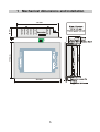
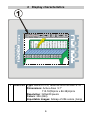
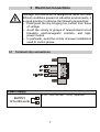
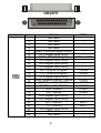
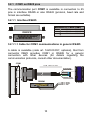
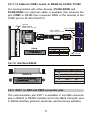
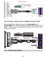
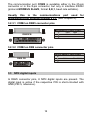
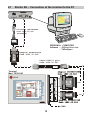
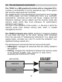
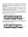
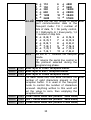
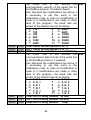
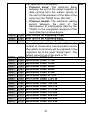
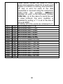
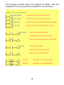
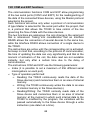
Manuale
User manual
TABLE OF CONTENTS
Introduction..................................................................................4
Model identification .....................................................................4
1 Mechanical dimensions and installation .............................5
2 Display characteristics..........................................................6
3 Electrical connections...........................................................7
3.1 Terminal clip connections ..................................................7
3.2 Serial ports of communication............................................8
3.2.1 COM1 on DB25 pins ..................................................10
3.2.2 EXP1 on DB9 and DB25 connector pins....................11
3.2.3 COM2 Interface RS232..............................................13
3.3 NPN digital inputs ............................................................14
4 Programming the terminal ..................................................15
4.1 Starter Kit – Connection of the terminal to the PC ...........16
4.2 The development environment ........................................17
4.2.1 Creation of a new project ...........................................19
4.2.2 Modification of an already existing project .................25
5 Memory areas of the TD320 ................................................26
5.1 Area of Variable V............................................................26
5.2 Area of Special Marker SM ..............................................27
5.3 Area of Digital Input I .......................................................40
5.4 Area of Digital Output Q...................................................40
5.5 Area of Marker M .............................................................41
5.6 Area of Analog Inputs AI ..................................................41
5.7 Area of Analog Outputs AQ .............................................41
5.8 Areas of Timer T and Preset Timer PT ............................41
5.9 Area of Counters C and Preset Counters PV...................42
5.10 Area of Bistable Relay B ...............................................42
5.11 Area of EEProm ............................................................42
5.12 Area of MMC.................................................................43
5.13 Area of TX/RX COM1 ...................................................43
5.14 Area of TX/RX EXP1.....................................................43
6 Communication protocols ..................................................45
6.1 Managing the communication port...................................45
6.1.1 Ports COM1 and EXP1 ..............................................46
6.1.2 Port COM2.................................................................46
2
6.2 Protocol ModBus RTU .....................................................46
6.2.1 ModBus RTU Master .................................................47
6.2.2 ModBus RTU Slave ...................................................48
6.3 Protocol NAIS Matsushita Master ....................................52
7 Ladder programming of the TD320 ....................................56
7.1 Digital input contacts I......................................................56
7.2 Digital output contacts Q..................................................56
7.3 Bistable relay B................................................................56
7.4 Timer T ............................................................................57
7.5 Counters C.......................................................................58
7.6 Mathematic formulas (FM) ...............................................59
7.7 MOV assignments ...........................................................59
7.8 BLKMOV multiple assignments .......................................59
7.9 MOVIND indexed assignments........................................60
7.10 MOVTXT assignments..................................................60
7.11 Digital input immediate contacts II ................................60
7.12 Contacts IF ...................................................................61
7.13 Functions SBIT and RBIT .............................................61
7.14 BIT contacts..................................................................61
7.15 RANGE functions..........................................................61
7.16 NOT contacts................................................................62
7.17 P and N contacts ..........................................................62
7.18 SEND functions ............................................................62
7.19 TunePOS and POS functions .......................................63
7.20 COM and EXP functions ...............................................66
7.21 StartPID, PID and SetOutPID functions ........................67
7.22 GENSET functions........................................................70
7.23 CONV functions ............................................................71
8 Notes / Updates....................................................................73
3
Introduction
Thank you for having chosen a instrument. Model TD320
is a graphical touch screen terminal with an integrated PLC
adapted for the supervision and control of systems where the
participation of an operator (HMI) is necessary. The graphical
resources are easily manageable from TdDesigner, a simple and
versatile development environment, while the logic relative to the
PLC is managed from the PLProg development environment,
which is common to other devices (PL250, TCT500, etc).
The waterproof protection of the facade is IP54 and IP30 for the
container.
Model identification
Only one version of the terminal TD320 is available, in low
voltage, AC or DC. This is indicated in the model identification.
Ordering code
TD320Power
AD 12…24V AC/DC ±15% 50/60Hz
4
1 Mechanical dimensions and installation
DB9 FE
204 mm
5
142 mm
170 mm
DB25 FE
4
48 mm
179 mm
2 Display characteristics
1
DISPLAY Type: Back-lit LCD, resistive touch screen STN
Dimensions: Active Area 5.7”
115.18(W)mm x 86.38(H)mm
Resolution: 320x240 pixels
Colors: 256 (8bit)
Importable Images: bitmap of 256 colors (.bmp)
6
3 Electrical connections
Although this instrument is designed to resist the most
difficult conditions present in industrial environments, it
is good practice to observe the following precautions:
• Distinguish the line bringing live current from those
of voltage
• Avoid the vicinity of groups of telecommand circuit
breakers, electromagnetic contacts, and highpower motors.
• In particular, avoid the vicinity of power installations
used to control phase.
3.1 Terminal clip connections
Power supply
• 12…24V AC/DC ±15% 50/60Hz
SUPPLY
12 to 24V ac/dc
7
Alarm output
With active contact (contact capacity
3A/250V~ resistive load) the voltage
+V (power) is available between clips
1(+) and 2(-).
3.2 Serial ports of communication
TD320 terminal communication with other devices is possible
through serial connection with RS485, RS232 and RS422.
The electrical signals are available in two connectors present at
the back of the terminal: post DB9 and post DB25.
DB9 FE
CONNECTOR PIN NUMBER
DB9 PINS
1
2
3
4
5
6
7
8
9
SIGNAL
Not used
RX – RS232 Program
TX – RS232 Program
RS485 GND RS485 / RS232
TX – RS232
RX – RS232
Not used
RS485 +
8
PORT
COM2
COM2
EXP1
EXP1 / COM2
EXP1
EXP1
EXP1
DB25FE
CONNECTOR
PIN N.
DB25
PINS
1
2
3
4
5
6
7
8
9
10
11
12
13
14
15
16
17
18
19
20
21
22
23
24
25
SIGNAL
PORT
Not used
Not used
Not used
Not used
GND (Common digital input)
DI1 (digital input NPN)
GND – RS232 Program
COM2 / EXP1
DI2 (digital input NPN)
DI3 (digital input NPN)
DI4 (digital input NPN)
RX – RS232 Program
COM2
TX – RS232 Program
COM2
DI5 (digital input NPN)
GND isolated RS485 / RS422
COM1
RS485+ / TX+ RS422
COM1
RS485- / TX- RS422
COM1
RX+ RS422
COM1
RX- RS422
COM1
DI6 (digital input NPN)
DI7 (digital input NPN)
RX – RS232
EXP1
TX – RS232
EXP1
DI8 (digital input NPN)
Not used
Not used
9
3.2.1 COM1 on DB25 pins
The communication port COM1 is available in connection to 25
pins in interface RS485 or also RS422 (protocol, baud rate and
format are settable).
3.2.1.1 Interface RS485
DB25FE
PIN 14
GND
PIN 15
RS485+
PIN 16
RS485-
3.2.1.1.1 Cable for COM1 communications in generic RS485
A cable is available (code art. 1620.00.057, optional), that from
connector DB25 provides COM1 in RS485 for a generic
connection with other devices (for details regarding the
communication protocols, consult other documentation).
COM1
Code 1620.00.057
DB25 FE
BLACK GND
WHITE Rs485+
DB9 FE
GREEN Rs485-
DB25M
10
PIN 16 RS485PIN 15 RS485+
PIN 14 GND
PLC
3.2.1.1.2 Cable for COM1 comm. in RS485 for PL250 / PL300
Adapter
DB25M>PLUG8
Code 1620.00.029
by PIXSYS
COM1
PL250
For communication with other devices (PL250-XXAD and
PL300-XXAD) an (optional) cable is available that connects the
port COM1 in RS485 from connector DB25 of the terminal to the
COM1 port on PLUG of the PLC.
COM1 - PL250-xxAD
Cable RS485
Code 1620.00.048
SLA VE #
1
1
by PIXSYS
8
DB25
14 GND
15 RS485+
16 RS485-
PLUG
2
1
4
1
R U N- CO M
CORRESPONDENCE PIN Rs485
DB25M
SLA VE #
0 UT
[ 1. . 6 ]
[ 7..1 2 ]
[ 1. . 5 ]
[ 6..1 0 ]
DB9 FE
1
PL300
1620.00.048
Cavo RS485
IN
DB25 FE
8
Adattatore
RS485
RS232
PROGRAM.
COM1 - PL300-xxAD
3.2.1.2 Interface RS422
DB25FE
PIN 14
GND
PIN 15
PIN 16
TX+
TX-
PIN 17
PIN 18
RX+
RX-
3.2.2 EXP1 on DB9 and DB25 connector pins
The communication port EXP1 is available in the DB9 connector
pins in RS232 or RS485 interface and in the DB25 connector pins
in RS232 interface (protocol, baud rate, and format are settable).
11
3.2.2.1 Interface RS232
DB9 FE
PIN 5
GND
PIN 6
TX - RS232
PIN 7
RX - RS232
3.2.2.2 Interface RS485
DB9 FE
PIN 5
GND
PIN 9
RS485+
PIN 4
RS485-
3.2.2.2.1 Cable of EXP1 communications in generic RS485
A cable is available (code art. 1620.00.034, optional), which
provides EXP1 port from connector DB9 in RS485 for a generic
connection with other devices (for details regarding the
communication protocols, consult other documentation).
12
3.2.2.2.2 Cable of EXP1 comm. in RS485 for PL250 / PL300
For communication with other devices (PL250-XXAD and
PL300-XXAD) an (optional) cable is available that connects port
EXP1 in RS485 from connector DB9 of the terminal to port COM1
on PLUG of the PLC..
DB25 FE
DB9
5 GND
9 RS485+
4 RS485-
PLUG
2
1
4
by PIXSYS
CORRESPONDENCE PIN Rs485
PL250
DB9M
COM1 - PL250-xxAD
1
Adattatore
RS485
RS232 PROGRAM.
by PIXSYS
8
COM1 - PL300-xxAD
3.2.3 COM2 Interface RS232
13
1
R U N- C OM
EXP1
S LA VE #
1
PL300
1620.00.048
Cavo RS485
[1..6]
0 U T [ 7.. 12 ]
[1..5]
IN
[ 6.. 10 ]
DB9 FE
SL A VE #
1
Cable RS485
Code 1620.00.048
8
The communication port COM2 is available either in the 25-pin
connector or in the 9-pin connector, but only in interface RS232
(protocol MODBUS SLAVE, format 8,N,1, baud rate settable).
Usually this is the communications port used
programming the terminal through a PC (see Chapter 4).
for
3.2.3.1 COM2 on DB25 connector pins
PIN 7
DB25FE
GND
PIN 12
TX - RS232
PIN 11
RX - RS232
3.2.3.2 COM2 on DB9 connector pins
DB9 FE
PIN 5
GND
PIN 3
TX - RS232
PIN 2
RX - RS232
3.3 NPN digital inputs
In DB25 connector pins, 8 NPN digital inputs are present. The
digital input is active if the respective PIN is short-circuited with
GND (PIN 5, reference).
14
DB25FE
PIN 5
Reference
PIN 6
DI 1
PIN 8
PIN 9
DI 2
DI 3
PIN 10
PIN 13
PIN 19
PIN 20
PIN 23
DI 4
DI 5
DI 6
DI 7
DI 8
PIN 5
GND
PIN 5
GND
PIN 23
DI 8
Active Digital input
PIN 23
DI 8
Digital input not active
4 Programming the terminal
In order to program the terminal it is necessary to connect it to a
PC. The development kit (optional, code art. 2100.10.008)
provides the cable necessary for the connection and the
development environment to create applications.
Programming involves the communication port COM2, present in
both connectors, but only in interface RS232. There are 2
adapters on the side of the terminal that allow a user to program
the terminal through connector DB25 or through DB9.
15
4.1
Starter Kit – Connection of the terminal to the PC
SERIAL
USB
Converter USB>SERIAL
Code 1620.00.050
(OPTIONAL)
Adattatore
PC RS232
PROGRAM.
PERSONAL COMPUTER
Software : - PLProg Vers. 4.xx
- TdDesigner
Adapter DB9M>PLUG8
Code 1620.00.040
Cable PLUG 8 pins
Code 1620.00.047
1
8
1620.00.047
Cavo RS232
PROGRAMMAZIONE
8
1
Terminal
Mod. TD320-AD
DB9 FE
DB25 FE
Adattatore
RS485
RS232
PROGRAM.
Adattatore
RS485
RS232 PROGRAM.
COM2
16
4.2 The development environment
The TD320 is a HMI graphical terminal with an integrated PLC.
It allows a centralization of all the operational logic of the system
that must be supervised and controlled.
The graphical part of the development environment must manage
the visible pages and their fundamental items (e.g. synthesis,
push-buttons, numerical and text edit boxes, images) and the
interaction between various objects and the memory areas (the
memory areas which they must reference for push-buttons,
indicators and images).
The logic of the operation of the system, i.e. the way in which the
memory areas must interact among each other, is instead
managed by the PLC.
The TD320 terminal is also a PLC, therefore it manages graphics
on one hand, and logic on the other, leaving other connected
PLCs the sole task of "detecting the information" (e.g. digital and
analog inputs, encoders etc.) and "to control the actuators" (e.g.
digital and analog outputs etc.).
The development environment has two sub-environments:
• TdDesigner: manages all resources that are strictly related to
the graphics.
• PLProg: manages the interactions between the memory areas
of the terminal (Ladder code, common to other PLCs,
essentially the PL250 and TCT500).
APPLICATION
GRAPHICS
TdDesigner
LOGIC
PLProg4.xx
17
Any application managed by the TD320 terminal should therefore
be realized using both the development environments,
implementing therefore two different files strictly connected
between them.
The operation of the terminal anticipates a division of the time
dedicated to graphics management (implemented with
TdDesigner) and of the time dedicated to the management of the
PLC (implemented with PLProg 4.xx).
The default setup foresees an equal division of the execution
cycle: the terminal will execute the instructions inherent for
graphics for 50% of the time, and the Ladder instructions of the
PLC for the other 50% (cyclically).
Time dedicated to graphics
GRAFICA
GRAPHICS
PLC
Time dedicated to PLC
GRAPHICS
GRAFICA
PLC
GRAPHICS
GRAFICA
PLC
Time
The time division is settable by the user (see chapter 5). An
example is shown below in which 80% of the time is dedicated to
the graphics and 20% to the PLC.
Time dedicated to graphics
GRAPHICS
Time dedicated to PLC
PLC GRAFICA
PLC GRAFICA
GRAPHICSPLC
GRAPHICSPLC
Time
18
4.2.1 Creation of a new project
Start TdDesigner
Create new project
name_file.tdproj
Start PLProg 4.xx
Create new Ladder diagram
name_file.plp
Compile project
name_file.tdproj
Compile Ladder diagram
name_file.plp
Transfer project
to Terminal
19
1
2
3
4
5
6
7
To create a new project and transfer it to the terminal, follow the
procedure and described below:
1. Start TdDesigner: Start the TdDesigner software from the
Start\Program menu or from the Desktop icon (automatically
created at installation).
2. Create new project name_file.tdproj: Once the development
environment is opened, create a new project as shown in the
figure below:
Select terminal TD320 (320x240 pixel display 5,7”).
20
The development environment can put new project in a
directory automatically created or in a folder chosen by user.
Graphics management is handled in other documentation,
available with the development kit (code art. 2100.10.008)
and assumed here as known by the user.
3. Start PLProg 4.xx: Start the PLProg 4.xx software from the
Start\Program menu or the Desktop icon (automatically
created at installation).
4. Create new Ladder diagram file_name.plp: Once the
development environment is opened, create a new diagram as
shown in the figure below:
21
A window will now open in the center of the screen: select the
terminal TD320 in the item list Select CPU.
The guide to the software and the implementation of the
Ladder code is available with the development kit (code art.
2100.10.008) and assumed here as known by the user.
5. Compile project file_name.tdproj: Once the implementation
of the graphics is finished, it is necessary to compile the
project, as shown in the figure below.
22
This operation is necessary to make the project available as
soon as implemented to the development environment
PLProg 4.xx.
The compilation has effect only if PLProg is open and the
terminal TD320 has been selected as CPU.
6. Compile Ladder diagram file_name.plp: Once the Ladder
diagram sketch is finished, it is necessary to compile it, as
shown in the figure below.
It is this fundamental passage that creates the link between
the Ladder file just compiled in the development environment
of PLProg4.xx with the file previously compiled in the
development environment of TdDesigner.
Only with this operation will it be in fact possible to
communicate to the terminal also the instructions inherent to
the graphics of the created project.
23
At this point, if saved by PLProg, file file_name.plp will contain
both the PLC part and the graphical part (is not necessary that
the file .tdproj has the same name of the file .plp).
7. Transfer the project to the terminal: If the compilation was
successful, now one can carry out the download of the project,
as shown in the figure below. The procedure transfers both the
graphical part and the PLC part to the terminal
If the TD320 is connected correctly to the PC (see diagram of
section 4.1), during the transfer the terminal will show this figure
on the display:
24
At the end of the download, the terminal will execute the
instructions of the entire application.
4.2.2 Modification of an already existing project
In the case in which an already existing project must be modified,
follow the procedure below:
Start PLProg 4.xx
YES
Modify
graphics?
NO
Start TdDesigner and
modify project name_file.tdproj
For modifications
of only PLC parts,
it is not necessary
to start TdDesigner
Compile project
name_file.tdproj
Modify Ladder diagram
name_file.plp
Compile Ladder diagram
name_file.plp
Transfer project
to Terminal
25
For eventual modifications of only the PLC part (as outlined) it is
not necessary to start TdDesigner. The compilation of the project
file_name.plp will maintain the graphics unchanged and will
activate the modifications of the Ladder diagram.
5 Memory areas of the TD320
The TD320 makes memory areas available where it is possible to
read or to write program data. Access to the various areas can
occur through instructions that access a single bit (b), a byte (B), a
word (W) or a double word (D).
SIGN
V
SM
I
AI
Q
M
B
AQ
T
PT
C
PV
EEP
MMC
COM1
EXP
AREA
Area of Variable V
Area of Special Marker
Area of Digital Inputs
Area of Analog Inputs
Area of Digital Outputs
Area of Marker
Area of Bistable
Area of Analog Outputs
Area of Timer
Area of Preset Timer
Area of Counters
Area of Preset Counters
Area of EEPROM
Area of EEPROM data
Area of buffer TX/RX port COM1
Area of buffer TX/RX port EXP1
ACCESS
b, W, D
b, W, D
b, W
b, W
b, W
b, W
B
b, W
b, W
b, W
b, W
b, W
W
W
B
B
5.1 Area of Variable V
Area variable V is a memory area used by the program to retain
the data of the operations. It consists of 10000 locations of type
word (5000 double word). Access can occur through operations on
26
bits, words or double words. In the last case, the number of double
words always makes reference to the organization by words,
therefore in order to access consecutive double word variables it is
necessary to increment by 2.
The memorized values are maintained even in the absence of
power thanks to the rechargeable battery pad. Once charged, the
battery maintains memorized data for approximately 6 months.
ACCESS WORD
VW0
VW1
VW2
VW3
VW4
VW5
ACCESS DOUBLE WORD
VD0
VD1
VD2
VD3
VD4
5.2 Area of Special Marker SM
Area special marker SM is the memory area used to retain all the
data necessary for the Ladder program to interact with the TD320
hardware.
Some data are initialized at the start with default values indicated
in the table below. In this area are the storage words that manage
the events relative to the graphics, the PLC control bits and the
setup for the serial ports of communication.
The table below describes the content of each single location of
the special marker area, indicating the address for access through
the ModBus protocol and the operation allowed at this location (R
= read, W = write, R/W = read/write). The bits and words that do
not appear in the tables are not used.
27
SM N°
SM0
ModBus
Address
Description / Signification
1000 Bit state
Bit 0 Bit RUN/STOP (1 = RUN). At startup R/W
this bit is always forced ON (PLC in
RUN). In STOP the output relays of
the PLC are disabled.
Bit 1 Bit always ON for the first scan cycle R
of the main program. It becomes
used, for example, to execute a
subprogram of initialization.
Bit 2 Bit that allows use of a 60-second
R
clock impulse (ON for 30 seconds,
OFF for 30 seconds).
Bit 3 Bit that allows use of a 1-second R
clock impulse (ON for 0.5 seconds,
OFF for 0.5 seconds).
Bit 4 Bit clock of scan cycles that is active R
(ON) for a cycle and deactivated
(OFF) for the successive cycle. It can
be used as an input for counting
scan cycles.
Bit 6 Bit ON during the transmission R
phase of data on serial port COM1. It
is automatically switched OFF at the
end of the transmission.
Bit 7 Bit ON during the transmission R
phase of data on serial port EXP1. It
is automatically switched OFF at the
end of the transmission.
Bit 8 Bit ON during the transmission R
phase of data on serial port COM2. It
is automatically switched OFF at the
end of the transmission.
28
This bit, if set ON, enables the serial
port COM1 in "modem" mode. That
means that the timeout between one
character and another in reception is
automatically fixed to 40 mS.
Bit 10 This bit, if set ON, enables the serial
port EXP1 in "modem" mode. That
means that the timeout between one
character and another in reception is
automatically fixed to 40 mS.
Bit 11 This bit, if set ON, enables the serial
port COM2 in "modem" mode. That
means that the timeout between one
character and another in reception is
automatically fixed to 40 mS.
1001 Diagnostic bit anomaly / malfunction
Bit 0 Bit ON in case of loss of data kept in
the area “special marker” SM.
Bit 1 Bit ON in case of loss of data kept in
the area “variable V”.
Bit 2 Bit ON in case of loss of data kept in
the area “EEProm”.
Bit 4 Bit ON in case of reset of the CPU or
intervention of the watch-dog.
Bit 5 Bit ON in case of stack overflow in
the area reserved for RAM.
Bit 7 Bit ON in case of anomaly /
malfunction in the EEProm.
Bit 8 Bit ON in case of anomaly /
malfunction in the clock.
Bit 10 Bit ON in case of stack overflow of
the timer interrupt.
1002 Device address
Address (word) of ModBus protocol of the
device. At startup, if SM1.0 = 1, the value
becomes initialized to “1”, otherwise the
previously saved data is maintained.
Bit 9
SM1
SM2
29
R/W
R/W
R/W
R/W
R/W
R/W
R/W
R/W
R/W
R/W
R/W
R/W
SM3
1003 Cycle time
Time of the last scan cycle of the program
R
(resolution 100µS).
SM4 1004 Minimal cycle time
The minimal time found of the program scan R
cycle (resolution 100µS).
SM5 1005 Maximum cycle time
The maximum time found of the program
R
scan cycle (resolution 100µS).
SM6 1006 Interval of timer interrupt n° 1
SM7 1007 Interval of timer interrupt n° 2
Word that defines the interval of the timer R/W
interrupt.
The value can be set between 1 and 100 ms
(example:: SM6=1 1 ms, SM6=100 100 ms). For values of SM6 and SM7 not
between 1 and 100, the correspondent
interrupt is fixed to a default to 100 ms. At
startup they are both fixed to a default of 100
100 ms.
In the Ladder code of the two interrupts, it
is not allowed to use functions that
access the areas of EEPROM and MMC.
SM8 1008 LCD contrast
LCD display contrast 0…100 0…100%. R/W
At startup, if SM1.0 = 1, the value is
initialized to 50 50%, otherwise the
previously saved data is maintained.
SM9 1009 Minimal lamp time
LCD back-lighting display 1…1000 R/W
1…1000 minutes, 0 always lit.
At startup, if SM1.0 = 1, the value is
initialized to 0 always lit, otherwise the
previously saved data is maintained.
SM10 1010 Touch screen X
SM11 1011 Touch screen Y
Coordinates of the point of contact on the R
30
SM12 1012
SM13 1013
SM14 1014
SM15 1015
LCD display (X = 0…319, Y = 0…239)
X=0, Y=0 upper left corner
When the display is not being touched, X =
500, Y = 500
Touch screen FLAGS
Bit 0 Bit ON in case of event: up, down or R
auto-repeat.
Bit 1 Bit ON in case of down touch
R
(pressure on the display).
Bit 2 Bit ON in case of up touch (release
R
of pressure on the display).
Bit 3 Bit ON in case of touch pressure
R
(continuous pressure on the display).
Language
The number of languages for the text R/W
messages in the graphics is set from
TdDesigner .
This word defines the language for the
currently visualized text messages (if n is the
number of languages set by TdDesigner,
SM13 can vary from 0 to n-1).
At startup, if SM1.0 = 1, the value is
initialized to 0 first language, otherwise
the selected language is maintained.
Number of visualized page
Word that indicates the number of the R
visualized page (default 1, at startup the first
page is always visualized).
Number of page to visualize
Word that specifies the page number to R/W
visualize.
Writing the number corresponding to a page
physically created from the TdDesigner in
this word will cause an immediate jump to
that page; otherwise the visualized page will
remain as it was before.
After the page change, the word is set back
to 0 automatically.
31
At startup, if SM1.0 = 1, the value is
initialized to 0 no change of page,
otherwise the page previously chosen is
maintained.
SM16 1016 Area of last variable modified
Word that indicates (for a single scan cycle)
R
the index corresponding to the last area of
memory saved from the graphics.
In detail, indices correspond to these areas:
1
Area word V
2
Area word SM
3
Area word AI
4
Area word TR
5
Area word AQ
6
Area word I
7
Area word Q
8
Area word T
9
Area word PT
10
Area word C
11
Area word PV
12
Area double V
Area double SM
13
Area word M
14
Area word EEPROM
15
Area word MMC
16
Area byte TX COM1 17
Area byte RX COM1 18
Area byte TX EXP1
19
Area byte RX EXP1
20
Area byte TX COM2 21
Area byte RX COM2 22
SM17 1017 Memory area number of last variable modified
Word that indicates (for a single scan cycle) R
the number of the last area of memory saved
from the graphics. As an example, if the
graphics modifies the variable VW30, , there
will be, for the scan cycle following the
modification, SM16 = 1 and SM17 = 30. In
32
SM18 1018
SM19 1019
SM20 1020
SM21 1021
SM30 1030
SM31 1031
SM32 1032
SM33 1033
SM34 1034
SM35 1035
SM36 1036
the successive cycle the two areas will be
automatically reset to 0.
Time of buzzer activation (x10ms)
Time buzzer is active in multiples of 10ms. R/W
The default value is 0xFFFF = 65536 =
buzzer extinguished, which is set also at the
end of the activation. If SM18 = 0, the buzzer
will extinguish only by touch of the display.
TD320 digital outputs
Bit 0 Bit ON Output relay active R/W
(between clips 1 and 2 of voltage +V)
CPU percentage for graphics
Percentage of time used to execute R/W
instructions relative to the graphics. Possible
values 10... 90 10…90%, default 50 50% (half time to graphics and half to PLC).
CPU percentage for graphics of page change
Percentage of time used only to execute R/W
instructions relative to the change of a page.
Once executed, the effective management of
the time is decided by SM20.
Possible values: 10…90 10…90%, default
50 50%
Seconds
Internal clock seconds (0…59)
R/W
Minutes
Internal clock minutes (0…59)
R/W
Hours
Internal clock hours (0…23)
R/W
Days
Internal clock days (1…31)
R/W
Months
Internal clock months (1…12)
R/W
Year
Internal clock year (0…99)
R/W
Day of the week
Internal clock day of the week (0 Sunday, R/W
33
SM37 1037
SM38 1038
SM39 1039
SM40 1040
SM41 1041
6 Saturday)
Digital input filter
It is possible to filter digital input signals by R/W
imposing a time of delay. If the state of the
input changes, the new state will be
accepted only if the input is maintained for
the imposed time. The data will become
accepted after the filter has eliminated
disturbances and fixed the lines of the inputs
on stable values.
The TD320 supports filters with times of
delay between 0 and 50ms (default 10ms).
Digital inputs
Bit 0 Bit ON Digital input DI1 active
R
Bit 1 Bit ON Digital input DI2 active
R
Bit 2 Bit ON Digital input DI3 active
R
Bit 3 Bit ON Digital input DI4 active
R
Bit 4 Bit ON Digital input DI5 active
R
Bit 5 Bit ON Digital input DI6 active
R
Bit 6 Bit ON Digital input DI7 active
R
Bit 7 Bit ON Digital input DI8 active
R
Conf. COM1 in mode Free-port
Conf. EXP1 in mode Free-port
Conf. COM2 in mode Free-port
Word that enables the serial port to function R/W
in free-port mode and to set its parameters.
Enabling this mode, the communications
protocol using the serial port will be disabled,
allowing direct access to the functions of
transmission and reception of the data on the
port. These parameters are initialized at
startup to 0 (free-port mode disabled).
Bit 0÷3 These bits set the communication R/W
velocity of the serial port in the freeport mode according to the
following values (baud):
34
SM42 1042
SM43 1043
SM44 1044
SM45 1045
SM49 1049
SM53 1053
0 110
6 4800
1 150
7 9600
2 300
8 19200
3 600
9 28800
4 1200
10 38400
5 2400
11 57600
Bit 4÷7 These bits set the format of serial R/W
port communication data in the
free-port mode: 7-8 = number of
bits of data, N = No parity control,
O = Odd parity, E = Even parity, 1,2
= number of stop bits.
0 8, N, 1
6 8, N, 2
1 8, O, 1
7 8, O, 2
2 8, E, 1
8 8, E, 2
9 7, N, 2
3 7, N, 1
10 7, O, 2
4 7, O, 1
5 7, E, 1
11 7, E, 2
Bit 8
Bit set to “1” enables the free-port R/W
mode.
“0” returns the serial line control to
the protocol selected during the
programming phase.
Num. Byte in COM1 reception buffer
Num. Byte in EXP1 reception buffer
Num. Byte in COM2 reception buffer
For each serial line, this word contains the R/W
number of valid characters present in the
reception buffer. It is used in the free-port
mode to control the number of characters
received. Anything written to this word will
set the value to zero, thus emptying the
reception buffer.
COM1 serial baud rate (default 9600 baud)
EXP1 serial baud rate (default 9600 baud)
COM2 serial baud rate (default 57600 baud)
35
SM46 1046
SM50 1050
SM54 1054
SM47 1047
SM51 1051
SM55 1055
The value that is set defines the R/W
communication velocity of the serial line for
the ModBus protocol, if enabled (baud):
Note: Because the modifications are active, it
is necessary to set this word in the
initialization code. In case no modification is
made or if modifications are made in other
parts of the program, the baud rate will
remain at the default rate set at startup
4800
6
0 110
9600
1 150
7
19200
2 300
8
28800
3 600
9
4 1200
10 38400
5 2400
11 57600
COM1 serial format (default 8, N, 1)
EXP1 serial format (default 8, N, 1)
COM2 serial format (8,N,1 non modifiable)
The value that is set defines the R/W
communications data format of the serial line
for the ModBus protocol, if enabled.
Note: Because the modifications are active, it
is necessary to set this word in the
initialization code. In case no modification is
made or if modifications are made in other
parts of the program, the baud rate will
remain at the default rate set at startup.
8, N, 2
6
0 8, N, 1
8, O, 2
1 8, O, 1
7
8, E, 2
2 8, E, 1
8
7, N, 2
3 7, N, 1
9
4 7, O, 1
10 7, O, 2
5 7, E, 1
11 7, E, 2
COM1 RX/TX delay (default 20 mS)
EXP1 RX/TX delay (default 100 mS)
COM2 RX/TX delay (default 1 mS)
36
SM48 1048
SM52 1052
SM56 1056
SM57
SM58
SM59
SM60
SM61
SM62
SM63
SM64
SM65
SM66
SM67
SM68
SM69
SM70
SM71
SM72
1057
1058
1059
1060
1061
1062
1063
1064
1065
1066
1067
1068
1069
1070
1071
1072
R/W
The value set in mS defines:
• Protocol slave: The minimum delay
between the end of the serial reception of
data coming from the master device to
the start of transmission of the data of the
reply from the TD320 (max 100 mS).
• Protocol master: The maximum waiting
period between the start of the
transmission of interrogation data by the
TD320, to the completed reception of the
reply data from a slave device.
Num. Errors for signaling COM1
Num. Errors for signaling EXP1
Num. Errors for signaling COM2
The value set in this word defines the R/W
number of consecutive communication errors
after which an anomaly will be signaled in the
respective bit of the word “Serial state”. The
default value for all of the ports is 10.
Serial state COM1 1-16
Serial state COM1 17-32
Serial state COM1 33-48
Serial state COM1 49-64
Serial state COM1 65-80
Serial state COM1 81-96
Serial state COM1 97-112
Serial state COM1 113-128
Serial state COM1 129-144
Serial state COM1 145-160
Serial state COM1 161-176
Serial state COM1 177-192
Serial state COM1 193-208
Serial state COM1 209-224
Serial state COM1 225-240
Serial state COM1 241-256
37
SM73
SM74
SM75
SM76
SM77
SM78
SM79
SM80
SM81
SM82
SM83
SM84
SM85
SM86
SM87
SM88
1073
1074
1075
1076
1077
1078
1079
1080
1081
1082
1083
1084
1085
1086
1087
1088
These words contain the state of COM1
serial communication. Each bit of each word
signals a condition of missing communication
(off line) or error for each of the data
transmitted or received using the instructions
COM_1-256 (for
example, SM66.9=1
indicates an error in the instruction number
COM-154(…)). In the case of a serial line set
to slave protocol, the error condition is
signalled by putting a “1” in all of the bits of
the word SM57.
At startup, all of the words are initialized to 0.
Serial state EXP1 1-16
Serial state EXP1 17-32
Serial state EXP1 33-48
Serial state EXP1 49-64
Serial state EXP1 65-80
Serial state EXP1 81-96
Serial state EXP1 97-112
Serial state EXP1 113-128
Serial state EXP1 129-144
Serial state EXP1 145-160
Serial state EXP1 161-176
Serial state EXP1 177-192
Serial state EXP1 193-208
Serial state EXP1 209-224
Serial state EXP1 225-240
Serial state EXP1 241-256
38
R
SM89
SM90
SM91
SM92
SM93
SM94
SM95
SM96
SM97
SM98
SM99
SM100
SM101
SM102
SM103
SM104
SM105
SM107
SM109
1089
1090
1091
1092
1093
1094
1095
1096
1097
1098
1099
1100
1101
1102
1103
1104
1105
1107
1109
SM106 1106
These words contain the state of EXP1 serial
communication. Each bit of each word
signals a condition of missing communication
(off line) or error for each of the data
transmitted or received using the instructions
EXP_1-256
(for
example,
SM80.4=1
indicates an error in the instruction number
EXP-117(…)). In the case of a serial line set
to slave protocol, the error condition is
signalled by putting a “1” in all of the bits of
the word SM73.
At startup, all of the words are initialized to 0.
Serial state COM2 1-16
Serial state COM2 17-32
Serial state COM2 33-48
Serial state COM2 49-64
Serial state COM2 65-80
Serial state COM2 81-96
Serial state COM2 97-112
Serial state COM2 113-128
Serial state COM2 129-144
Serial state COM2 145-160
Serial state COM2 161-176
Serial state COM2 177-192
Serial state COM2 193-208
Serial state COM2 209-224
Serial state COM2 225-240
Serial state COM2 241-256
COM1 time-out number
EXP1 time-out number
COM2 time-out number
If the corresponding port Is set to a Master
protocol, this indicates the number of nonreceived packets of information during the
communication.
At startup, all counts are initialized to 0.
COM1 number of errors
39
R
R
SM108 1108 EXP1 number of errors
SM110 1110 COM2 number of errors
If the corresponding port Is set to a Master R
protocol, this indicates the number of packets
of information with errors during the
communication.
At startup, all counts are initialized to 0.
SM111 1111 COM1 minimum delay for new transmission#
SM112 1112 EXP1 minimum delay for new transmission#
SM113 1113 COM2 minimum delay for new transmission#
If the corresponding port is set to a Master R/W
protocol, this sets the minimum delay for a
new transmission after the reply of a slave
device.
Possible values 0…100 0…100ms,
default 5 5ms
5.3 Area of Digital Input I
Memory area I is composed of 32 words and can be used to
contain the state of the digital inputs read through the serial lines
of other devices.
It is organized in words: each of the 16 bits of a word can
represent the state of an input. It is accessible also in bits, in order
to allow the control of each single input.
5.4 Area of Digital Output Q
Memory area Q is composed of 32 words and can be used to
contain the state of the digital outputs to then write them on serial
lines of other devices.
# Available from firmware version 1.12
40
It is organized in words: each of the 16 bits of a word can
represent the state of an output. It is accessible also in bits, in
order to allow the control of each single output.
5.5 Area of Marker M
Memory area M is comprised of 50 words and contains the state
of all the markers (contact bits) used in the program.
It is organized in words: each of the 16 bits of a word represents
the state of a marker. For example, the state of the marker M5 is
memorized in the bit 4 of word 1 in memory area M. The marker
M5 is thus accessible as M1.4 (contact bit of the word), but also as
single bit M5 (contact or electrical relay coil).
5.6 Area of Analog Inputs AI
Memory area AI is composed of 32 words and can be used to
contain the state of the analog inputs read from the serial lines of
other devices.
It is organized in words: each can represent the state of an analog
input
5.7 Area of Analog Outputs AQ
Memory area AI is composed of 32 words and can be used to
contain the state of the analog outputs read from the serial line of
other devices
It is organized in words: each can represent the state of an analog
output.
5.8 Areas of Timer T and Preset Timer PT
The area of memory for timer T is composed of 128 words. If the
timer is enabled, the variation of the contents of the area of
memory is regulated by the type of timer, which is set at the
moment of activation.
41
The area of memory for preset timer PT is composed of 128
words and contains the values of activation of the contacts
(preset) of the respective timers.
The areas are organized in signed words, thus the resolution of
the timer and the preset timer is 16 bits (+32767).
5.9 Area of Counters C and Preset Counters PV
The memory area for counters C is composed of 64 words. If a
counter is enabled, the variation of the contents of the memory
area is regulated by the type of counter.
The memory area for preset counters PV is composed of 64
words and contains the values of activation of the (preset)
contacts of the respective counters.
The areas are organized in words, thus the resolution of the
counters and preset counters is 16 bits (from -32768 to +32767).
5.10 Area of Bistable Relay B
The area of memory for bistable relay B is composed of 128 bits.
It is organized by bits, thus each bistable relay is individualized by
a single bit.
5.11 Area of EEProm
The area of memory EEProm is composed of 1000 words. This
memory is storage for data that must be maintained even if the
TD320 remains off for very long periods (over 6 months). The data
saved in this area are in fact tested at startup to verify their
integrity, and any anomalies are signalled by activating the bit
SM1.2, causing the initialization of the entire area to 0.
Access and writing to this area require a time significantly longer
than any other (order of 30/40 mS), thus it is advisable not to use it
for continual access (there is also a limit to the number of times
that an EEProm cell can be written to, of an order of 1,000,000
times), but only to copy at startup the data stored here, for
42
example to memory area V, and then use area V for an access
that is more rapid (order of 5/10µs).
5.12 Area of MMC
The memory area MMC is composed of 3000 words. This is the
memory storage where it is possible to save large quantities of
data and maintain it even in the absence of power.
The memory is of type EEProm. The resulting access is thus
slower than area V and SM and the TD320 executes no control of
the integrity of the data stored in this area.
5.13 Area of TX/RX COM1
The memory area TX/RX COM1 is composed of 200 bytes. This
area is used to manage the data in transit on serial port COM1.
The first 100 bytes (TX-0…TX-99) are used to load the data to
transmit; the last 100 bytes (RX-0…RX-99) are used to save the
data received by the serial port COM1.
These bytes are useful only in the free-port mode, while in normal
mode they are managed directly by the protocol selected in the
programming phase.
5.14 Area of TX/RX EXP1
The memory area TX/RX EXP1 is composed of 200 bytes. This
area is used to manage the data in transit on the serial port EXP1.
The first 100 bytes (TX-0…TX-99) are used to load the data to
transmit, the last 100 bytes (RX-0…RX-99) are used to save the
data received by the serial port EXP1.
43
These bytes are useful only in the free-port mode, while in normal
mode they are managed directly by the protocol selected in the
programming phase.
44
6 Communication protocols
The TD329 can communicate with all devices that support the
following serial protocols:
•
•
ModBus RTU
Nais Matsushita master
The terminal has 3 serial ports of communication (COM1, EXP,
COM2), analyzed from the electrical point of view in chapter 3.
Nonetheless, the ports are each managed in a different manner
and will be analyzed separately.
6.1 Managing the communication port
The communication between the TD320 and other devices is
managed by the PLC part of the terminal, thus the configuration of
the port and the instructions must be implemented in the
development environment PLProg 4.xx.
Generally the coils of the Ladder diagram are executed following
the sequential order written in the diagram itself. The instruction
related to the coil at line “n+1” is not executed until the full
completion of the instruction related to the coil at line “n” (for coils
positioned in the same column).
The control of transmission and reception of data is instead
asynchronous with respect to the cycle of execution of the
Ladder code.
When an instruction of read/write of a device must be executed
(line “n”), control passes immediately to the next instruction (line
“n+1”), without waiting for the data to be effectively read/written.
45
The effective transfer of the data in the serial line is executed in a
manner that is independent to the normal scan of Ladder code, in
different times according to the port that is used.
6.1.1 Ports COM1 and EXP1
The ports COM1 and EXP1 can be configured with protocol
ModBus (master or slave), or Nais Matsushita master, Control
Technique. These are the ports typically used for communication
with other devices (PLC, etc.).
The control of the communication is carried out every 1 mS.
This means that the corresponding flow of serial data will be
controlled 1000 times a second.
6.1.2 Port COM2
The port COM2 can be configured only by using protocol ModBus
slave. This port is used for programming the terminal by PC.
The control of the communication is carried out every scan
cycle of the Ladder code.
This means that the flow of the data in the serial port COM2 will be
controlled one time at the end of each scan cycle.
6.2 Protocol ModBus RTU
The ModBus on the serial line is a Master-Slave protocol. In a
network with this type, there is a single node (the Master) that
interrogates and commands the Slaves and processes the results.
The Slave nodes typically do not transmit data unless specifically
requested by the Master and do not communicate directly between
each other.
A device in the serial line (a network node) is uniquely determined
by an identification number (ID, variable from 1 to 255), called the
ModBus Slave address: two devices cannot have the same
address.
46
The addressees of a request (one or more Slave nodes) are
selected by the Master by their ID, thus the data that transits on
the line has a precise destination.
The Master controls the line: it doesn’t have a specific ID address
and can read or write data in words or bits with one or more Slave
devices, specifying the destination ID.
Data read or written is saved in the destination device in registers
identified by a specific ModBus address (variable from 1 to
65535). Each ModBus address can correspond to a register (word
area of memory) or a single bit of a register (particular bit of an
area of memory).
Refer to the following figure for the list of possible operations in a
ModBus communication: reading and writing of a word or bit,
single or multiple.
Main features of protocol Modbus RTU
Baud-rate
Programmable
Format
8,N,1 (8 bit, no parity, 1 stop) (default)
Supported
BITS READING
(0x01, 0x02)
function
WORDS READING (max 30 word)
(0x03, 0x04)
SINGLE BIT WRITING
(0x05)
SINGLE WORD WRITING
(0x06)
MULTIPLE BITS WRITING
(0x0F)
MULTIPLE WORDS WRITING (max 30 word) (0x10)
Error codes
ILLEGAL FUNCTION CODE
(0x01)
ILLEGAL DATA ADDRESS
(0x02)
ILLEGAL DATA VALUE
(0x04)
Broadcast
Simultaneus writing to all connected slaves using
address 0x00 and no answer from slaves.
Polling
with Polling using address 0xFF, any connected slave can
unknown
slave answer
address
6.2.1 ModBus RTU Master
The protocol ModBus Master can be configured only for the ports
COM1 and EXP1.
47
With this configuration the TD320 will have control of the transit of
the data of the corresponding port. For each of the two ports, there
can be active up to 256 frames (active packets) at the same time.
Each frame corresponds to an instruction of direct communication:
•
•
•
Reading from a Slave: Reading from the slave at the
ModBus address corresponding to the data of interest is
memorized in the registers of the Master. Each instruction can
read up to 16 consecutive words.
Writing on a Slave: Data of interest by the Master is written in
the slave at the ModBus address corresponding to the data to
overwrite. Each instruction can write up to 16 consecutive
words.
Read/write on a Slave: Normally data read from the slave is
saved in the Master. When the data internal to the TD320
varies by effect of the program, it is useful to write the modified
data into the Slave. Each instruction of read/write can operate
only on 1 word.
6.2.2 ModBus RTU Slave
The protocol ModBus Slave can be configured for all three of the
ports COM1, EXP1, and COM2.
With this configuration all of the resources of the terminal are
available to the Master device that is eventually connected.
The following table indicates all of the data (word and bit)
accessible by use of the ModBus protocol. Each area of memory
corresponds to a distinct ModBus address (for the access of a
word or a bit), variable from 0 to 65536.
The read/write access and the value given at startup of the TD320
are shown for each. Depending upon the initialization values, the
following cases occur:
48
1. “ROM” fixed values defined by the program.
2. “EEP”, value stored in EEProm memory, maintained for at
least 10 years even in the absence of power..
3. “BUFF”, value stored in RAM with the battery buffer. Also this
data is maintained in the absence of power, but for a limited
time (around 4 to 6 months).
4. “DEFINED VALUE” the value given to the data at startup
corresponds to the value indicated in the table.
ACCESS TO WORD
MODBUS
ADDRESS
0
1
2
3
4
5
6
10
1000 ÷ 1199
2000 ÷ 2999
12000 ÷ 12127
13000 ÷ 13127
14000 ÷ 14063
15000 ÷ 15063
16000 ÷ 16099
16500 ÷ 16599
17000 ÷ 17099
17500 ÷ 17599
18000 ÷ 18099
18500 ÷ 18599
DESCRIPTION
Type of device
Version of Firmware
Protocol activated on COM1
Protocol activated on EXP1
Protocol activated on COM2
Address of protocol
Version of BOOT
Clock seconds TD320
Word area special marker SM
Word area variable V
Word area timer T
Word area preset timer PT
Word area counter C
Word area preset counters PV
Word area buffer TX COM1
Word area buffer RX COM1
Word area buffer TX EXP1
Word area buffer RX EXP1
Word area buffer TX COM2
Word area buffer RX COM2
49
READ/
WRITE
RESET
VALUE
R
R
R
R
R
R
R
R/W
R/W
R/W
R/W
R/W
R/W
R/W
R
R
R
R
R
R
ROM
ROM
ROM
ROM
ROM
BUFF
ROM
BUFF
BUFF
BUFF
0
0
0
0
0
0
0
0
0
0
19000 ÷ 19031
19200 ÷ 19215
19400 ÷ 19431
19800 ÷ 19927
Word area analog input AI
Word area trimmer TR
Word area analog output AQ
Word percentage proportional
/ integral / derived / output PID
19800
% Action proportional PID1
19801
% Action integral PID1
19802
% Action derived PID1
19803
% Output PID1
19804
% Action proportional PID2
……
……
19927
% Output PID128
20000 ÷ 20999 Word area EEProm
30000 ÷ 59999 Word area MMC
R
R
R
0
0
0
R
R
R
R
R
0
BUFF
BUFF
BUFF
0
R
R/W
R/W
BUFF
EEP
EEP
ACCESS TO WORD
MODBUS
ADDRESS
DESCRIPTION
(n.o. = “normally open”)
READ/
WRITE
RESET
VALUE
90
Contacts n.o. positioners
POS1÷POS16
Contacts n.o. tuning positioners
POS1÷POS16
Contacts n.o. digital inputs I1 ÷ I16
Contacts n.o. digital inputs I17 ÷ I32
……
Contacts n.o. digital inputs I497 ÷ I512
Contacts n.o. digital outputs Q1 ÷ Q16
Contacts n.o. digital outputs Q17 ÷ Q32
……
Contacts n.o. digital outputs Q497 ÷
Q512
Contacts n.o. bistable relays B1 ÷ B16
Contacts n.o. bistable relays B17 ÷ B32
……
R
0
R
0
R
R
0
0
R
R
R
0
0
0
R
0
R/W
R/W
0
0
95
100
101
……
131
150
151
……
181
200
201
……
50
207
250
251
……
299
300
301
……
307
350
351
352
353
Contacts n.o. bistable relays B113 ÷
B128
Contacts n.o. marker M1 ÷ M16
Contacts n.o. marker M17 ÷ M32
……
Contacts n.o. marker M785 ÷ M800
Contacts n.o. timer T1 ÷ T16
Contacts n.o. timer T17 ÷ T32
……
Contacts n.o. timer T113 ÷ T128
Contacts n.o. counters C1 ÷ C16
Contacts n.o. counters C17 ÷ C32
Contacts n.o. counters C33 ÷ C48
Contacts n.o. counters C49 ÷ C64
R/W
0
R
R
0
0
R
R
R
0
0
0
R
R
R
R
R
0
0
0
0
0
ACCESS TO BIT
MODBUS
ADDRESS
DESCRIPTION
(n.o. = “normally open”)
READ/
WRITE
RESET
VALUE
1440
1441
……
1455
1520
1521
……
1535
1600
1601
……
2111
2400
2401
……
2911
3200
Contact n.o. positioner POS1
Contact n.o. positioner POS2
……
Contact n.o. positioner POS15
Contact n.o. tuning position POS1
Contact n.o. tuning position POS2
……
Contact n.o. tuning position POS15
Contact n.o. digital input I1
Contact n.o. digital input I2
……
Contact n.o. digital input I512
Contact n.o. digital output Q1
Contact n.o. digital output Q2
……
Contact n.o. digital output Q512
Contact n.o. bistable relay B1
R
R
0
0
R
R
R
0
0
0
R
R/W
R/W
0
0
0
R/W
R/W
R/W
0
0
0
R/W
R/W
0
0
51
3201
……
3327
4000
4001
……
4799
4800
4801
……
4927
5600
5601
……
5663
16000
16001
……
19199
32000
32001
……
63999
Contact n.o. bistable relay B2
……
Contact n.o. bistable relay B128
Contact n.o. marker M1
Contact n.o. marker M2
……
Contact n.o. marker M800
Contact n.o. timer T1
Contact n.o. timer T2
……
Contact n.o. timer T128
Contact n.o. counter C1
Contact n.o. counter C2
……
Contact n.o. counter C64
Bit 0 area special marker SM0
Bit 1 area special marker SM0
……
Bit 15 area special marker SM199
Bit 0 area variables V0
Bit 1 area variables V0
……
Bit 15 area variables V2000
R/W
0
R/W
R/W
R/W
0
0
0
R/W
R
R
0
0
0
R
R
R
0
0
0
R
R/W
R/W
0
BUFF
BUFF
R/W
R/W
R/W
BUFF
BUFF
BUFF
R/W
BUFF
6.3 Protocol NAIS Matsushita Master
This is the protocol that permits the reading and writing of data (bit
of word) of the PLC Nais Matsushita.
Generally, the communications interface is RS232, the velocity is
9600 baud (bits/sec), the format of communications 8,O,1 (8 bits
of data, odd parity, 1 stop bit).
The following table indicates all of the elements that can be
read/written from the PLC. The address of the bit o of the word to
read or write is obtained by adding the real address of the bit/word
(between Min and Max) to the value indicated in the column
Offset. Each instruction “COM” or “EXP” can read or write to
several consecutive data locations, the maximum number for each
52
type of data is indicated in the column “Max number bit/word
read/written consecutively”.
ACCESS TO BIT
MAX NUMBER
OF BITS READ /
WRITTEN
CONSECUTIVELY
CONTACT
SYM
MIN
MAX
OFFSET
READ/
WRITE
EXTERNAL
INPUT
EXTERNAL
OUTPUT
INTERNAL
RELAY
LINK
RELAY
TIMER
COUNTER
X
0
9999
0
R
Y
0
9999 10000
R/W
8
R
0
9999 20000
R/W
8
L
0
9999 30000
R/W
8
T
C
0
0
9999 40000
9999 50000
R
R
8
8
MAX NUMBER
OF WORDS READ
/ WRITTEN
CONSECUTIVELY
ACCESS TO WORD
8
WORD NAME
SYM
MIN
MAX
OFFSET
READ/
WRITE
EXTERNAL
INPUT
EXTERNAL
OUTPUT
INTERNAL
RELAY
LINK
RELAY
TIMER
COUNTER
INDEX
REG. X
INDEX
REG. Y
X
0
999
0
R
Y
0
999
1000
R/W
10(R) / 7 (W)
R
0
999
2000
R/W
10(R) / 7 (W)
L
0
999
3000
R/W
10(R) / 7 (W)
T
C
0
0
0
999
999
0
4000
5000
6000
R
R
R/W
10
10
1
0
0
6001
R/W
1
53
10
INDEX
REG. D
DATA
REGISTER
LINK DATA
REGISTER
FILE
REGISTER
SET VALUE
AREA
ELAPSED
VALUE
AREA
0
0
6002
R/W
1
DT
0
9999 10000
R/W
10(R) / 7 (W)
LD
0
9999 20000
R/W
10(R) / 7 (W)
FL
0
9999 30000
R/W
10(R) / 7 (W)
0
9999 40000
R/W
10(R) / 7 (W)
0
9999 50000
R/W
10(R) / 7 (W)
For the two examples shown below, the protocol NAIS Matsushita
is selected for the port EXP1.
The illustrated instructions that follow write the contents of the 8
words from V10 to V17 of the TD320 in the register EXTERNAL
OUTPUT of the PLC NAIS from Y3 to YA (Y10).
54
The following illustration, however, reads the register DATA
REGISTER of the PLC NAIS, the 10 words from DT0 to DT9, and
copies them in the area of V0 to V9 of the TD320.
55
7 Ladder programming of the TD320
Programming the PLC part of the TD320 is accomplished with the
development environment PLProg 4.xx, which provides the user
with all the resources necessary for creation of the Ladder
diagram.
The compilation and download procedure discussed in chapter 4
allows the TD320 terminal to achieve the desired functionality.
The following describes all available elements (contacts and coils)
and the relative characteristics for the creation of the diagram.
7.1 Digital input contacts I
Digital input contacts I can contain the state of the inputs read via
serial lines of other devices, up to a maximum of 512.
A contact normally open (N.O.) is closed (ON) when the bit value
is “1” (input active). A contact normally closed (N.C.) is opened
(ON) when the bit value is “0” (input non-active).
7.2 Digital output contacts Q
The TD320 has 512 type “Q” outputs. These can be used to
contain the state of eventual outputs of other devices,
communicated by serial lines.
Each output has a coil and a related logical contact N.O. (normally
open) or N.C. (normally closed). At activation of the coil “Q”, the
related logical contact will close (if normally open) or will open (if
normally closed).
7.3 Bistable relay B
There are 128 bistable relays available in the TD320. Each has a
coil and related logical contact normally open or closed (N.O/N.C).
At activation of coil “B”, the related logical contact will change
state, if it was closed it will open, if it was open it will close. A
contact N.O. is closed (ON) when the bit value is “1”. A contact
56
N.C. is opened (ON) when the bit value is “0”. At the startup of the
terminal, a contact N.O. will be open.
7.4 Timer T
The TD320 has 128 timers of 16 bits. Each is available in three
modes of functioning:
• TON “on-delay” of activation: time begins counting when the
coil is activated (ON). The timer bit (contact T) will be activated
when the current timer value (word T) becomes greater than or
equal to the pre-established time (preset, word PT). When the
coil is deactivated (OFF), the current value of the timer is reset
(zeroed). The timer stops in any case when it reaches the
maximum value in signed 16-bits (+32767).
• TOFF “off-delay” of deactivation: allows delaying the
deactivation of an output for a given period of time after the
input has been deactivated. When the coil is activated (ON),
the time bit (contact T) is immediately activated and the current
value of the timer (word T) will be set to “0”. At the deactivation
of the coil, the timer will count until the elapsed time becomes
greater than or equal to the pre-established time (preset, word
PT). Once reached, the timer bit deactivates and the current
value stops advancing. If the input remains inactive for a time
that is less than the pre-established time, the timer bit remains
active. To start the count, the TOFF operation should sense a
transition from state active to non-active (ON OFF)
• TONR with memory: time begins counting when the coil is
active (ON). The timer bit (contact T) is active when the current
timer value (word T) becomes greater than or equal to the preestablished time (preset, word PT). When the coil is
deactivated (OFF), the current value of the timer is maintained.
Thus it is possible to accumulate time for more periods of
activation of the coil. The current value of the timer can be
reset with the operation MOV(Tx = #0). The timer stops in any
case when it reaches the maximum value in signed 16-bits
(+32767).
57
The time base can be selected between 10 mS, 100 mS, and 1S
for each mode of functioning.
The current value of the timer is a multiple of the selected time
base. For example, a current value of 50 in a timer with a base
time of 10 mS corresponds to 500 mS, and with a base time of 1 S
corresponds to 50 S.
The preset timer (PT) value can be a constant, or the contents of
an area VW, SMW, AI, or TR.
7.5 Counters C
The TD320 has 64 counters of 16 bits. These are available in two
modes of functioning:
• MUP forward counter: the counter bit (contact C) is activated
when the current value (word C) is greater than or equal to the
pre-established value (PV). The counts increments each time
the input of the up-count Cx(UP) is active and decrements
each time the input of the down-count Cx(DOWN) is active.
The counter will be set to zero upon activation of the reset
input Cx(RESET) or when the operation MOV(Cx=#0) is
executed. Upon reaching the maximum value (32767), the rise
of the next up-count will leave the current value unchanged.
Similarly, upon reaching the minimum value (-32768) the rise
of the next down-count will leave the current value unchanged.
For the forward counters, the pre-established value (PV) is
compared with the current value at the end of each cycle of
the program. If the value is greater than or equal to the preset
value, the counter bit activates (counter C), otherwise it is
deactivated.
• MDOWN backward counter: the counter bit (contact C) is
activated when the current value (word C) becomes equal to
zero. The counter decrements from a pre-established value
(PV) on the rise of the input of down-count Cx(DOWN) and
increments on the rise of the input of up-count Cx(UP). Upon
reaching the maximum value (32767), the rise of the next upcount will leave the current value unchanged. The counter
resets the count bit (contact C) and loads the preset value
58
(PV) when the input Cx(RESET) becomes active. The counter
in backward mode will stop counting when it reaches zero.
The preset value (PV) can be a constant, or the contents of an
area VW, SMW, AI, or TR.
7.6 Mathematic formulas (FM)
The functions of math formulas FM execute mathematical
operations (+, -, *, /, | [OR: logical inclusive or], & [logical AND], ^
[XOR: logical exclusive or], << [ROL: ROtate shift Left], >> [ROR:
ROtate shift Right) between two operators and saves the result in
another memory location. The operators can be numeric
(constants) or refer to the available areas of memory (variables).
7.7 MOV assignments
The function MOV (move) assigns a numeric value (constant) or
the contents of another location (source area) to a specified
location in memory (destination area).
An instruction such as MOV(A=B) copies the contents of the
memory location B to the memory location A.
7.8 BLKMOV multiple assignments
The function BLKMOV (block move) assigns a numerical value or
the value from another (source) block of memory to a destination
block of memory.
An instruction such as BLKMOV(Ai=Bi, num. data 8) copies the
contents of memory Bi into the location of memory Ai, the contents
of location Bi+1 into the location Ai+1, ……and the contents of
Bi+7into the location Ai+7.
59
7.9 MOVIND indexed assignments
MOVIND (move with index offset) assigns a numerical value
(constant) or the value from another location of memory (variable
source) to the specified location of memory (destination) as offset
by an index for the source and/or destination.
This type of assignment permits various memory areas to be used
as vectors of N locations each, where the value taken from
another location is used as an “index”. It is possible to access the
values n=0, n=1, …, n=N-1 of the area.
An instruction such as MOVIND(A[B]=C[D]) copies the contents of
the memory location C[D] into the location A[B]. The index of area
C is specified by D, which can be another memory location, and
similarly B is the index of area A.
7.10 MOVTXT assignments
MOVTXT saves string characters passed as a function parameter
to a specified location in memory. This function permits the
following types of characters of the string in the memory area:
• ONE_CHARACTER_PER_WORD: in this format, each word of
the destination area will contain a single character of the
source string.
• TWO_CHARACTERS_PER_WORD in this format, each word
in the destination area will contain two characters of the
source string, starting with the high part. If string = “Example”
then V[0] = Ex, V[1] = am, V[2] = pl. V[3] = e.
7.11 Digital input immediate contacts II
The digital input contacts II allow the immediate reading of the
digital input state. The contact normally open is closed (ON) when
the bit value is “1” (input active). The contact normally closed is
open (ON) when the bit value is “0” (input non-active).
60
7.12 Contacts IF
The operations of conditional IF compare the values of two
variables of any area of memory. It is possible to carry out the
following types of comparison: = (equal), >= (greater than or
equal), <= (less than or equal), > (more than), < (less than), <>
(not equal). The contact is active when the comparison is true.
7.13 Functions SBIT and RBIT
The function SBIT (set bit) puts a “1” in a bit of a memory area
when the coil of the function is at the active state.
The function RBIT (reset bit) puts a “0” in a bit of a memory area
when the coil of the function is at the active state.
The index of the bit varies from 0 to 15 (the destination area is
always a word), where bit 0 is the least-significant bit (LSB).
7.14 BIT contacts
This operation extracts the value of a bit of an area of memory.
A contact normally open is closed (ON) when the bit value is “1”.
A contact normally closed is open (ON) when the bit value is “0”.
The index of the bit varies from 0 to 15 (the destination area is
always a word), where bit 0 is the least-significant bit (LSB).
7.15 RANGE functions
The function RANGE defines the value of the minimum and maxim
limits for the analog inputs AI, for the trimmer TR, for the analog
outputs AQ, and for the outputs of the PID.
RANGE( AI1, Min 10, Max 200)
The function imposes a minimum limit of 10 and maximum limit of
200 for the analog input AI1. If the analog input AI1 corresponds to
a potentiometer (from a PLC via a serial communication), is used
to establish the preset (PT) of a timer of base time 100 mS, this
61
provides a variable time from 1.0 to 20.0 seconds, according to the
value of the potentiometer.
If input values exceed the limits set in the RANGE function, the
output will be blocked to the minimum or maximum allowed value.
As for the output PID, the minimum and maximum values serve to
calculate the value of the output generated by the algorithm of
regulation. Let us consider the following example:
RANGE( PID1, Min 100, Max 500 )
The function imposes the minimum limit of 100 and the maximum
limit of 500 for the PID1 output. This means that an output of 0%
corresponds to the minimum value imposed (100) and 100% will
correspond to an output equal to the maximum value (500).
7.16 NOT contacts
The contact NOT modifies the state of the flow of current. The flow
of current stops if it reaches a NOT contact and supplies energy if
it doesn’t reach it.
The operation NOT inverts the logical value (0 1 and 1 0).
7.17 P and N contacts
The transition positive P contact activates the flow of current for
one scan cycle of each transition from OFF to ON. The transition
negative N contact activates the flow of current for one scan cycle
of each transition from ON to OFF.
The instructions that follow in the diagram are thus executed only
once (per scan cycle) for each transition that activates the contact.
7.18 SEND functions
The function SEND transmits the data through the serial line in
free-port mode.
In this mode, enabled by the special markers SM39, SM40, and
SM41, the protocol that normally manages the serial port is
disabled and the Ladder program takes control of the port and of
the transmission and reception buffers.
62
After having loaded the buffer with the data to transmit, activating
the SEND function, which has parameters for the serial port and
the number of characters to transmit, will cause the data to be sent
on the serial line.
During the transmission phase, the bits SM0.6, SM0.7 or SM0.8
relative to the transmission port are set to “1”, while at the end of
the transmission they will be set to “0”. It is possible to control an
eventual reply of a connected device through the control of SM42,
SM43, and SM44, which contain the number of characters
received and saved in the reception buffer of each serial port. Any
writing on any of these special markers causes the emptying of the
buffer data in reception of the corresponding port.
Calls to the SEND function before the end of the preceding
transmission or with free-port mode disabled are ignored by the
program.
7.19 TunePOS and POS functions
The function “TunePOS” executes an auto-tuning procedure,
indispensable for extracting the data of reaction time and axis
inertia for which a positioning procedure is requested.
The function “POS” executes the positioning ON/OFF of the axis.
The functions operate on the variable area VD (double word), the
address of the beginning of the area is requested as a parameter
of the functions “TunePOS” and “POS”. The following table
indicates how the data are organized in the area of the two
functions from the address of the specified location:
Address
area VD
+0
+2
+4
+6
+8
Contents
Count for encoder
Counts for setpoint positioning
Counts for absolute maximum gap of positioning
Time needed to attain max velocity (in decimals of
seconds)
State of the positioning output (0=stationary,
1=forward, 2=backward)
63
+10
+12
+14
+16
+18
+20
Counts for forward inertia
Counts for backward inertia
Duration of minimum impulse (resolution 0.2 mS)
Counts of movement after impulse of 100 mS
Counts of movement after impulse of 500 mS
Counts of movement after impulse of 1000 mS
For correct functioning, it is necessary to proceed as follows:
• Transfer the count of the encoder connected to a remote
device (read via a serial line) in the field “Counts for encoder”
(beginning area of memory).
• Set the count values to the desired position of the axis in the
field “Counts for setpoint positioning”.
• Set the count values for the maximum gap of positioning in the
field “Counts for absolute maximum gap of positioning”.
• Set the time, in decimals of seconds”, needed for the axis to
attain maximum velocity.
• Activate the function “TunePOS” and wait that the contact
TunePOS (normally open) closes to indicate the end of the
procedure of auto-tuning the axis. At this point, the inertia data
and the reaction time of the axis are automatically memorized
in the indicated area of memory, remaining available for the
function “POS”.
• Deactivate the function “TunePOS”.
• Activate the function “POS”. When the axis is positioned to the
setting imposed (within the pre-established gap), the contact
POS (normally open) will close, to indicate the end of
positioning.
• Activate the outputs FORWARD and BACKWARD, reading
the value of the field “Output” (VD+8). If the value of “Output”
is “1”, it is necessary to activate the output FORWARD, if it is
“-1”, it is necessary to activate the output BACKWARD, if it is
“0” it is not necessary to activate any output.
• Set the value of the field “Output” to zero when the consent of
the function “TunePOS” or “POS” is removed, to avoid that the
output remains forced to forward or backward.
64
The following example shows the segment of Ladder code that
implements the axis positions as explained in the procedure:
65
7.20 COM and EXP functions
The communication functions COM and EXP allow programming
of the two serial ports (COM1 and EXP1) for the reading/writing of
the data of the connected Slave devices, using the Master protocol
selected in the project.
Such functions are active only when a protocol of communication
of type Master is selected for the serial port within the project, that
is, a protocol that allows the TD320 to take control of the line
governing the flow of data with the slave devices.
The two functions are analogous, the only change is the serial port
that is referenced. Taking into consideration that an Interface
RS485 allows the connection of several devices to the same line,
while the Interface RS232 allows connection of a single device to
the TD320.
The instructions are active until the corresponding coil is activated,
but keep in mind that, according to the protocol of communication,
the time of updating the data can vary significantly and that at the
moment of activation of the coil, the data read are not available
instantly, but only after a certain time due to the delay of
communication.
The instructions COM and EXP use the following parameters:
• Index (it is possible to set a maximum of 256 different serial
interrogations on each port).
• Type of operation performed:
• Reading: the TD320 continuously reads the data of the
Slave device(s) and memorizes them in an area of internal
memory.
• Writing: the TD320 continuously writes the data to an area
of internal memory in the Slave device(s).
• Reading/Writing: the TD320 normally reads data of the
Slave device and memorizes them in an area of internal
memory; at the moment in which such internal data to the
TD320 is modified by the program, the variations will be
passed automatically to the Slave device through a write
instruction (one datum at a time).
66
•
•
•
•
•
Number of the Slave (address of communication of the Slave
device).
The type of data (word or bit).
The address ModBus relative to the datum (or data) to transfer.
The area of internal memory of the PL250A for reading or
writing the data.
The number of words (the instructions of reading and writing
can transfer up to consecutive 16 bits/words).
7.21 StartPID, PID and SetOutPID functions
The functions StartPID, PID and SetOutPID allow the regulation of
a size through an algorithm of action that is proportional, integral,
and derived.
The function StartPID activates the regulation. The function can
be activated a single time at startup or repeated at a later moment
permitting the modification “on the fly” of the parameters of
regulation. The integral action of the PID is zeroed only by calling
the functions and fixing the integral time to “0”. Otherwise, even in
case of shutdown, the system will initialize the regulation
maintaining as point of departure the same percentage of integral
action, thus limiting the time of transition.
Parameters of the function StartPID:
• Proportional band
• Integral time
• Derived time
• Dead band
The parameters can be inserted in numerical format, or can refer
to areas of memory. The integral time is expressed in the units of
time in which the function PID is called (for instance, function PID
called every 1 second, integral time expressed in seconds). The
derived time, however, is expressed with an additional decimal
digit with respect to the integral time. The proportional band and
the dead band are instead expressed in numeric values equal to
the setpoint and the process to regulate.
67
The parameters of the function PID:
• Setpoint
• Process
• Output value
• Type of regulation action
The PID function, after acquiring setpoint, process, type of action
and type of output, will set in the variable “Ouput value” the value
obtained in the algorithm of regulation. Such a value will be
obtained rescaling the percentage of the value between 0 and
10000 (0.00% ÷ 100.00%) between the minimum and maximum
value of the PID output set by the RANGE function.
The following table indicates 8 types of regulation and the
modulation intervals (the effective value between the interval is
determined also by the actions integral and derivative, the table
shows only the proportional components):
Type of regulation action
Intervals of modulation
Output 100%
Single direct action, 0
Output 0%
Setpoint
Setpoint - P.B. / 2
Setpoint + P.B. / 2
Output 100%
Single direct action, 1
Output 0%
Setpoint
Setpoint - P.B. / 2
Setpoint + P.B. / 2
Output 100%
Single inverse action, 0
Output 0%
Setpoint
Setpoint - P.B. / 2
68
Setpoint + P.B./ 2
Output 100%
Single inverse action, 1
Output 0%
Setpoint
Setpoint - P.B. / 2
Setpoint + P.B./ 2
Output 100%
Double direct action, 0
Output 0%
Setpoint + P.B. / 2
Setpoint
Setpoint + P.B.
Output 100%
Double direct action, 1
Output 0%
Setpoint + P.B. / 2
Setpoint
Setpoint + P.B.
Output 100%
Double inverse action, 0
Output 0%
Setpoint - P.B. 2
Setpoint
Setpoint - P.B.
Output 100%
Double inverse action, 1
Output 0%
Setpoint - P.B. / 2
Setpoint - P.B.
Setpoint
The PID function, for correct operation, must be called at the most
regular intervals possible, thus by timer, or for more brief and
precise times, by an internal interrupt.
The function SetOutPID is used for the regulation anticipated by
the double function automatic/manual. It serves to avoid oscillation
of size control in switching from manual mode to automatic by the
PID algorithm.
69
The function uses the following parameters:
• Output value
The Output value is set by the PID automatically calculating the
single percentages of the proportional and integral actions. In this
mode, at the switching of manual function to automatic, the output
value of the PID will take on the value set by manual and will
initiate the regulation.
The function thus should be called only during the manual
regulation phase, in order to maintain alignment of the output of
the PID with that of manual. The function will automatically zero
the derived action. The use of this function with the process
outside of the proportional band sets the integral action to zero.
7.22 GENSET functions
The function GENSET automatically generates a setpoint variable
rising or falling, with the possibility to set a ramp of acceleration or
deceleration. The function GENSET operates on a series of
variables in contiguous double words, starting from the location
indicated as a parameter to the function.
The following table indicates how the data are organized in the
memory area used by the function starting from the address of the
specified location:
Address
area VD
+0
+2
+4
+6
Contents
State of the GENSET function
0 Stop or end of movement
1 Initialization function
2 Ramp of acceleration
3 Movement at constant velocity
4 Ramp of deceleration
Initial setpoint / setpoint calculated by the function
GENSET (counts)
Final setpoint (counts)
Velocity of movement (counts*1000 / time unit)
70
+8
+10
+12
Duration of acceleration ramp (time unit)
Duration of deceleration ramp (time unit)
Instantaneous velocity of setpoint (counts*1000 / time
unit)
For correct functioning, it is necessary to proceed as follows:
• Set the starting setpoint in location VD+2.
• Set the final setpoint in location VD+4.
• Set the maximum velocity of movement in location VD+6 in
counts*1000 / time unit (so as to have 3 decimal digits. For
example, setting 12345 corresponds to a velocity of 12.345
counts / time unit).
• Set the duration of the acceleration ramp in location VD+8
(expressed in time units, if the duration of the phase of
acceleration should be 1 second, and the GENSET function is
called by an interrupt of 1 mS, set 1000).
• Set the duration of the ramp of deceleration in location VD+10.
• Write “1” in the location VD (the location indicated as
parameter of the function). This gives the “start” to the function
that will automatically begin to write the generated setpoint in
the location VD+2. The location VD will be also updated with
the actual state, while the instantaneous velocity of the
setpoint expressed with three decimal digits will be written in
the location VD+12.
At the end of movement, when the location VD+2 attains the value
of the final setpoint, the functional will automatically enter into a
standby phase, indicated by the value “0” in the location VD. In
this mode, the GENSET function can remain always enabled,
even when movement is not necessary.
7.23 CONV functions
The function CONV converts the source data into one of the
available formats:
• TO_7SEG_SIGNED: Converts the input data (a word with sign
–32768..+32767) into a number specified in digits already
transformed in code for 7-segment display. The function will
71
•
take as parameters the number of digits to convert, starting
from the least significant digit. The coded data will be saved
(one digit per word) starting from the destination word and
then in the successive words according to the number of digits
requested.
TO_7SEG_UNSIGNED: This is analogous to the above
description with the difference that the data of origin is
interpreted as a word without sign (0..65535). The code is
comprised of a bit set to “1” if a segment should be lit, and “0”
if the segment should remain dark. The association between
the bits and the segments of the display is the following:
B0
B5
B6 B1
B4
B2
B3 B7
•
TO_ASCII_SIGNED: Convert the input data (a word with sign
–32768..+32767) into ASCII-coded digits. The function will
take as parameters the number of digits to save. The coded
data will be saved (one digit per word) starting from the
destination word and then in the successive words according
to the number of digits requested.
•
TO_ASCII_UNSIGNED: This is analogous to the above
description with the difference that the data of origin is
interpreted as a word without sign (0..65535).
72
8 Notes / Updates
73
Notes / Updates
74
Notes / Updates
75