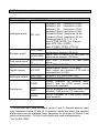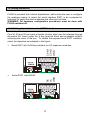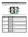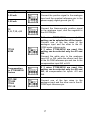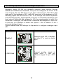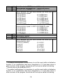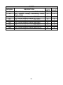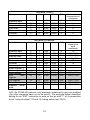
1
User manual
2
1 Acquisition and actuation module PL260 .........................5
1.1 Introduction ......................................................................................... 5
1.2 Front panel and main features ........................................................... 6
1.3 Main hardware features ...................................................................... 7
1.4 Size and installation ........................................................................... 8
1.5 Electrical wiring................................................................................... 9
1.5.1 Connectors and terminal blocks.................................................. 9
1.5.2 Connection of sensors to analogue inputs ................................ 12
1.5.3 Connection of a load cell ........................................................... 13
1.5.4 Connection of a bidirectional encoder....................................... 14
1.5.5 Connect PL260 to RS485.............................................................. 14
1.6 Setting dip-switch ............................................................................. 15
1.6.1 Setting dip-switch to select EXP1 interface .............................. 15
1.6.2 Setting dip-switch to select analogue input AI1..4 .................... 16
1.6.3 Setting dip-switch to select analogue intput AI5..6 ................... 18
1.6.4 Setting PL260 protocol address ................................................ 20
1.7 PL260 memory areas ....................................................................... 21
1.7.1 Variables V memory area ......................................................... 21
1.7.2 Memory area “special marker SM”............................................ 22
1.7.3 Memory area "digital inputs I" ................................................... 44
1.7.4 Memory area "digital outputs Q" ............................................... 44
1.7.5 Memory area "support marker M" ............................................. 44
1.7.6 Memory area "analogue inputs AI" ........................................... 44
1.7.7 Memory area "analogue outputs AQ" ....................................... 44
1.7.8 Memory area "timer T" .............................................................. 45
1.7.9 Memory area "preset timer PT"................................................. 45
1.7.10 Memory area "counters C" ...................................................... 45
1.7.11 Memory area preset values of counters PV ............................ 45
1.7.12 Memory area EEPROM .......................................................... 45
1.7.13 Memory area MMC ................................................................. 46
1.7.14 Memory areas COMx_SEND and EXP1_SEND .................... 46
1.7.15 Memory areas COMx_RECEIVE and EXP1_RECEIVE ......... 46
1.8 Modbus RTU slave communication protocol .................................... 47
1.9 Addresses word/bit of PL260 for protocol Modbus RTU .................. 48
2 PL260 Ladder programming ............................................ 53
2.1 Introduction ....................................................................................... 53
2.2 Elements of Ladder programming .................................................... 53
2.2.1 Contacts digital inputs I ............................................................ 53
2.2.2 Digital outputs Q........................................................................ 53
2.2.3 Bistable relays B ....................................................................... 54
2.2.4 Timer T ...................................................................................... 54
2.2.5 Counter C .................................................................................. 55
3
2.2.6 Mathematical formule FM function ............................................ 55
2.2.7 Assignement function MOV ...................................................... 56
2.2.8 Assignement function BLKMOV................................................ 56
2.2.9 Indexed Assignement Function MOVIND ................................. 56
2.2.10 Assignement function MOVTXT.............................................. 56
2.2.11 Contacts II immediate digital inputs ....................................... 56
2.2.12 Immediate outputs QI .............................................................. 57
2.2.13 IF contact ................................................................................ 57
2.2.14 SBIT and RBIT functions ........................................................ 57
2.2.15 BIT contact ............................................................................. 57
2.2.16 RANGE function ..................................................................... 57
2.2.17 Contact NOT ........................................................................... 58
2.2.18 Contact P and N ...................................................................... 59
2.2.19 Function SEND and mode Free-port ...................................... 59
2.2.20 Function TunePOS and POS (positioning axis ON/OFF) ....... 59
2.2.21 Function serial communication COM and EXP ....................... 61
2.2.22 MapEXP mapping function for external I/O ............................ 64
2.2.23 Functions StartPID , PID , SetOutPID .................................... 67
2.2.24 Functions StartPOSPID and POSPID..................................... 68
2.2.25 Function GENSET................................................................... 69
2.2.26 Function CONV ....................................................................... 71
4
1 Acquisition and actuation module PL260
1.1 Introduction
The PL260 is a compact PLC for the acquisition of analogue and digital
signals and the execution of complex mathematical functions. One of the
most important features on PL260 is the logic blocks, which allow simple
management of complex operations.
The module may be placed beside the plant to control and communicate
with a central controller through RS-485 (galvanically isolated), allowing
simplified signal wiring and increased noise immunity. The DIN rail
mounting housing has been developed according to CE requirements for
light and heavy industry.
Main features
Operating
conditions
Box
Sealing
Weight
Dimensions
Temperature 0-45 °C,
Humidity 35..95uR%
DIN rail mounting, self-extinguishing UL94 V0
Box IP30
Approx. 350 gr.
90 x 160, depth 58 mm
Order codes:
PL260 Outputs
1
1
Inputs
2
Power-supply
16 static outputs
4 analogue 0..10V
4 analogue inputs, 16 bit resolution
16 digital inputs
2 bidirectional encoders
4 analogue inputs, 16 bit resolution
16 digital inputs
5 fast count inputs
AD 12…24V DC
5
1.2 Front panel and main features
1
2
6
N°
1
2
3
4
5
6
3
4
5
4
5
Description
Plug connector for serial communication COM1 and COM2
Green led RUN:
• ON
PLC is in RUN mode and is executing the instructions
programmed by ladder language.
• Slowly flashing
0,5 s on / 0,5 s off) PL260 is used as I/O
module (no ladder program loaded).
• Fast flashing
(0,2 s on / 0,2 s off) only boot program is loaded
on PL260 (no main program and no ladder application)
Yellow led COM:
• ON
for 50mS during transmission of each frame on one of the
available serial ports
• ON
always during ladder programming or maintenance of PLC
(updating main program)
Expansion terminal block for COM1 and EXP1 serial
Terminal block for digital inputs with led to signal active input
Terminal block for digital outputs with led to signal active outputs
Power-supply terminal block, analogue inputs/outputs
6
1.3 Main hardware features
Hardware
Power-supply
Analogue inputs
Encoder inputs
1
Fast count inputs
2
Digital inputs
Digital outputs
Analogue outputs
Serial ports
12...24 Vdc 6VA
Voltage 0-10V (resolution 10 bit)
Voltage 0-10V (resolution 16 bit)
Voltage 0-1V
(resolution 16 bit)
Voltage 0-20mV (resolution 16 bit)
Current 0-20mA (resolution 16 bit)
AI1..AI4
Current 4-20mA (resolution 16 bit)
Thermocouple K, S, T, R, J, E
Input PT100, NI100 (2 or 3 wires)
Input NTC-10K = β3435
Input PT1000, PT500, PTC-1K
Inputs PNP (0-24VDC) or 1st input for
I1/A1÷I2/B1
bidirectional encoder (25 KHz)
Inputs PNP (0-24VDC) or 2nd input for
I3/A2÷I4/B2
bidirectional encoder (25 KHz)
I1,I2,I15,I16, Input PNP (0-24VDC) or fast count
I3
inputs.
I1÷I16
Inputs PNP (0-24VDC)
Static outputs: 24Vdc - 0,7A max.
Q1÷Q16
Each output can produce 0.7A with a
combined limit of 4.0A.
AQ1÷AQ2
Voltage 0-10V (resolution 8 bit)
AQ3÷AQ4
Voltage 0-12,5V (resolution 14 bit)
RS485 available on terminal block
COM1
(A,B,C) and on COM plug-8 poles
(galvanically isolated).
RS232 available on terminal block (non
EXP1
isolated). CAN bus for I/O expansion.
RS232 available on COM plug-8 poles
COM2
(non isolated).
1
First encoder input uses hardware inputs I1 and I2. Second encoder input
uses hardware inputs I3 and I4. If encoder inputs are used, the relevant
digital inputs are not available. Max. frequency for encoders is 25 KHz if not
used contemporarily, 15 KHz if both inputs are used contemporarily.
2
On PL260-12AD.
7
45
90
1.4 Size and installation
43
53
160 mm
8
5
1.5 Electrical wiring
1.5.1 Connectors and terminal blocks
N°
1
Name
+
2
3
4
5
6
7
8
9
10
11
12
AI.1
AI.2
AI.3
AI.4
AI-COM
AQ.1
AQ.2
AQ.3
AQ.4
AQ-COM
21
+V
45
13
14
I1 / A1
I2 / B1
Description
Power-supply 12÷24V DC 6VA. To improve noise immunity,
the use of a dedicated supply is recommended.
Analogue input AI1 positive signal
Analogue input AI2 positive signal
Analogue input AI3 positive signal
Analogue input AI4 positive signal
Common negative signal for analogue inputs
Analogue output AQ1 positive signal (0÷10 VDC)
Analogue output AQ2 positive signal (0÷10V DC)
Analogue output AQ3 positive signal (0÷12,5 VDC)
Analogue output AQ4 positive signal (0÷12,5 VDC)
Common negative signal for analogue outputs
Common positive signal for digital inputs. Connect this signal
to one of the digital inputs I1÷I16, to activate inputs. Voltage
available on these pins can supply sensors to connect to the
analogue inputs (N.B.: on these pins the available supply is
Vcc, not stabilized!).
Digital input
PL260-11AD: input for
bidirectional encoder no.
1 (phase A)
Digital input
PL260-12AD: input for
To activate digital
fast counter no. 1
inputs, short-circuit
PL260-11AD: input for
signal +V on the
bidirectional encoder no.
input pin.
1 (phase B)
PL260-12AD: input for
fast counter no. 2
9
N°
Name
Description
15 I3 / Z1 / A2 Digital input
PL260-11AD: input for
bidirectional encoder no.
1 signal Zero, or input
for bidirectional encoder
To activate digital
no. 2 phase A.
inputs, switch
PL260-12AD: input for terminal +V to the
input terminal.
fast counter no. 5
16
I4 / B2
Digital input
17
18
19
20
37
38
39
40
41
42
I5
I6
I7
I8
I9
I10
I11
I12
I13
I14
Digital input
Digital input
Digital input
Digital input
Digital input
Digital input
Digital input
Digital input
Digital input
Digital input
43
I15
Digital input
44
I16
Digital input
22
23
24
25
26
27
28
29
46
47
48
49
50
51
52
Q1
Q2
Q3
Q4
Q5
Q6
Q7
Q8
Q9
Q10
Q11
Q12
Q13
Q14
Q15
Static output
Static output
Static output
Static output
Static output
Static output
Static output
Static output
Static output
Static output
Static output
Static output
Static output
Static output
Static output
Input for bidirectional
encoder no. 2 (phase
B)
To activate digital
inputs, switch
terminal +V to the
input terminal.
PL260-12AD: input for
fast counter no. 3
PL260-12AD: input for
fast counter no. 4
Output 24Vdc 0,7A max.
Each output can
produce 0,7A for a
max. combined
consumption of
4.0A.
10
N°
53
30
54
31
32
33
34
35
36
Name
Q16
Description
Static output
+VDC
Static outputs power-supply.
B
A
C
CANH/RX
CANL/TX
GND
Signal RS+
Signal RSSignal RS REF
Signal CAN+ or RX (RS232)
Signal CAN- or TX (RS232)
Ref. signal for serial EXP1
N°
Name
COM1
RS485
COM1 interface
RS485
EXP1
interface
CAN or RS232
Description
PL260
plug-8
87654 - COM1-A RS- (MORS. 32)
32 - COM1-C RS REF (MORS. 33)
1 - COM1-B RS+ (MORS. 31)
8
1
COM1
RS485
PLUG
RJ45
COM2
RS232
Connect
12÷24 VDC
PL260
plug-8
876 - COM2- RX232
5 - COM2- TX232
43 - COM2- GND232
21-
8
1
COM2
RS232
11
1.5.2 Connection of sensors to analogue inputs
Below some examples of connection for common sensors to the analogue
inputs of the PL260.
+V
+
(21)
0-20mA
4-20mA
2 wires
+V
+
(21)
-
0-10V
0-20mA
4-20mA
3 wires
1
12
2
PT100/NI100
a 3 fili
1.5.3 Connection of a load cell
Below some examples of connection for a load cell to the analogue inputs of
PL260.
SIGNAL SUPPLY
+
+
SHIELD
Weight Cell
As showed in the figure, to connect a load cell to the PL260 it is necessary to:
•
•
•
•
Create the voltage (max 5 Vdc) to supply the cell through the analogue
output AQ4.
Connect the load cell signals + and – to the analogue inputs AI1 (signal +)
and AI2 (signal -) for reading the differential voltage generated.
Configure the reference to convert input AI1 on AI2 (SM82 = 2).
Configure analogue input AI1 on 0..20 mV (SM40 = 4).
13
1.5.4 Connection of a bidirectional encoder
Below an example of connection for a typical bidirectional encoder (phase A,B
and Z optional) which can be connected to the PL260 inputs.
+ V (21)
A
B
Z
+
1.5.5 Connect PL260 to RS485
Below an example of connection for more modules PL260 to RS485 line for
the communication with a master device.
+ - REF
USARE CAVO SCHERMATO TWISTATO
14
220 ohm
1.6 Setting dip-switch
PL260 is provided with internal dipswitches, which allow the user to configure
the analogue inputs, to select the serial interface EXP1 to be connected to
terminals, to select the device address and other plc functions.
WARNING: All hardware configuration procedures must be done with
PL260 switched off.
1.6.1 Setting dip-switch to select EXP1 interface
Pins 34, 35 and 36 can have a double function which can be selected through
dip-switch S6, found under the 6 way terminal block and accessible without
removing the cover of the box. To enable the required serial EXP1 interface,
select the dipswitch as indicated in the figure:
Serial EXP1 with CAN-bus interface for I/O expansion modules
•
Serial EXP1 with RS232.
RX
TX
GND
CAN H
CAN L
GND
•
15
1.6.2 Setting dip-switch to select analogue input AI1..4
Each analogue input can be configured through a 4 way dip-switch, the
correspondence between the inputs and the relative dip-switch is showed in
the figure below:
AI4
AI3
AI2
AI1
To obtain the required input type, it is necessary to set the relative dip-switch
as indicated in the table below:
Input type
Dip-switch
Notes
Disabled
If the analogue input is not used, leave all
switches off as showed in the figure.
0..10V 10 bit
Connect the positive signal to the analogue
input, and the reference signal to the pin
AI-COM.
0..10V 16 bit
Connect the positive signal to the analogue
input, and the reference signal to the pin
AI-COM.
0..1V
0..20 mV
Connect the positive signal to the analogue
input, and the reference signal to the pin
AI-COM.
16
Input type
0..20 mA
4..20 mA
Dip-switch
Notes
Connect the positive signal to the analogue
input and the eventual reference pin to the
power-supply digital ground (pin 2).
TC
K, S, T, R, J, E
Connect the thermocouple positive signal
to the analogue input, and the negative to
the AI-COM pin.
PT100
NI100
If 2 wires PT100/NI100 are used, this
setting can be selected for all the inputs.
Connect one of the two wires to the
analogue input and the other to the AICOM inputs reference pin.
If 3 wires PT100/NI100 are used, this
setting can be selected only for AI1 and
AI4.
Connect the white wire to the analogue
input AI1 or AI4, while the others (red) one
to the AI-COM reference pin and one to the
compensation input AI2 or AI3.
Compensation
for PT100/NI100
3 wires
If 3 wires PT100/NI100 are used, this
setting can be selected only for AI2 and
AI3, as compensation for inputs AI1 and
AI4.
NTC-10K
PT1000
PT500
PTC-1K
Connect one of the two wires to the
analogue input and the other one to the AICOM input reference pin.
17
1.6.3 Setting dip-switch to select analogue intput AI5..6
Analogue inputs AI5..AI6 are generally selected (reset setting) through
SMW44 and SMW45 as "Disabled". They can be configured as 0..10V 10 bit
only if inputs AI1 and AI2 have not yet been selected as 0..10V 10 bit. AI5
uses part of the hardware of AI1, while AI6 uses part of the hardware of AI2.
Selecting inputs AI5 and AI6 as 0..10V 10 bit through the relative dip-switch
(see following figures), signal applied to input I7 is converted to analogue, the
read value is deducted and assigned to AI5; the signal applied to input I8 is
converted to analogue, the read value is deducted and assigned to input AI6.
In this way it is possible to obtain two inputs 0..10V in addition to the 4
universal analogue inputs.
Figures below show the settings for dip-switch to configure analogue input
AI5.
Input AI5
Dip-switch
Notes
Analogue input AI5 is disabled
and input I7 is used as digital
input.
Disabled
Connect positive signal to
digital input I7, and the
reference signal to pin -VDC
(2).
0..10V 10 bit
18
Figures below show the settings for dip-switch to configure analogue input
AI6.
Input AI6
Dip-switch
Notes
Disabled
Analogue input AI6 is disabled
and input I8 is used as digital
input.
0..10V 10 bit
Connect positive signal to
digital input I8, and the
reference signal to pin -VDC
(2).
19
1.6.4 Setting PL260 protocol address
Two dip-switches are provided to configure the address of module for serial
communication with a master device. There are 4 available combinations of
these dip-switch. To connect more than 4 devices to the same network it is
necessary to change the address offset value.
The address is given as follows:
MODULE ADDRESS = ADDRESS OFFSET + DIP-SWITCH COMBINATION
The offset address, value stored on PL260 memory (default "1"), can be
modified by writing on SMW4 word.
Dip-switch combinations are:
Dip-switch combination = 0
Dip-switch combination = 1
Dip-switch combination = 2
Dip-switch combination = 3
20
1.7 PL260 memory areas
The PL260 module provides the user with memory areas where it is
possible to read or write program data. Memory areas can be entered by
instruction with access by single bit (B), by word (W) or double word (D).
CODE
V
SM
I
AI
Q
M
AQ
T
PT
C
PV
EEP
MMC
COM1_TX
COM1_RX
EXP1_TX
EXP1_RX
COM2_TX
COM2_RX
AREA
Variables V area
Special Marker area
Digital inputs area
Analogue inputs area
Digital outputs area
Marker area
Analogue outputs area
Timer area
Preset Timer area
Counters area
Preset counters area
EEPROM area
EEPROM_MEMORY area
COM1_TX area
COM1_RX area
EXP1_TX area
EXP1_RX area
COM2_TX area
COM2_RX area
ACCESS
B, W, D
B, W, D
B, W
B, W
B, W
B, W
B, W
B, W
B, W
B, W
B, W
W
W
W
W
W
W
W
W
1.7.1 Variables V memory area
The memory area “Variables V” is the memory which is used by the
program to store data of operations. It is composed by 350 locations, type
word (16 bit) or 175 double words (32 bit). This area may be edited by
operations on bit, word or double word. The number of double word still
refers to the words structure, therefore a single double word uses 2 single
word addresses (eg. VD0=VW0+VW1)
21
The values are stored also in case of power failure thanks to a
rechargeable back-up battery. After charging, the battery stores data for
approx. 6 months
1.7.2 Memory area “special marker SM”
This area is the memory which contains all data used by the ladder
program to interact with the hardware resources of PL260. Some of this
data is initialized when starting the PLC with the default values described in
the table below. This area contains all data related to analogue inputs,
trimmers, counts and set values of encoders, and also some bits controlled
by the PLC for the ladder application as well as the settings for serial ports.
The table below includes the content of each single location of the area
“Special markers”, giving the address for Modbus protocol and the type of
operation
allowed
for
each
location
(R=reading,
W=writing,
R/W=reading/writing).
22
SM n° Mod.
Description / meaning
word
SM0
1000 Status bit
Bit 0
Bit 1
Bit 2
Bit 3
Bit 4
Bit 5
Bit 6
Bit 7
Bit 8
Bit 9
RUN/STOP bit (1=run). At starting this bit is
always forced to ON, obtaining the RUN mode
of PLC. In STOP mode, the relay outputs of
PLC are disabled.
This bit is always ON for first scanning cycle
of main program. Eg. It is used to execute
initialization subprogram.
This bit makes available a clock impulse of 60
seconds (ON for 30 seconds, OFF for 30
seconds).
This bit makes available a clock impulse of 1
second (ON for 0,5 second, OFF for 0,5
second)
This bit is a clock of scanning cycle, which is
active ON for one cycle and disabled OFF for
following cycle. It may be used as counting
input for scanning cycle.
Bit TEST. Setting this bit as ON, the reading
of digital inputs is disabled. Status of inputs is
read on word SM37. Setting this word, it is
possible to execute debug/test of the program
simulating input starting.
This bit is ON during the transmission of data
to serial port COM1. It is automatically set to
OFF at the end of transmission
This bit is ON during the transmission of data
to serial port EXP1. It is automatically set to
OFF at the end of transmission.
This bit is ON during the transmission of data
to serial port COM2. It is automatically set to
OFF at the end of transmission.
If set to ON this bit enables mode “modem” for
serial port COM1. This means that Timeout
between one character and the other
character in receiving mode is automatically
set to 40mS.
23
R/W
R
R
R
R
R/W
R
R
R
R/W
Bit 10 If set to ON this bit enables mode “modem” for
serial port EXP1. This means that Timeout
between one character and the other
character in receiving mode is automatically
set to 40mS.
Bit 11 If set to ON this bit enables mode “modem” for
serial port COM2. This means that Timeout
between one character and the other
character in receiving mode is automatically
set to 40mS.
Bit 12 If set to 1, this bit disables internal clock
reading/writing, making faster program
execution.
Bit 13 If set to 1, this bit disables counters C[1..16]
and enables timers T[49..64], normally
disabled.
SM1
R/W
R/W
R/W
R/W
1001 Diagnostic Bit (faults/anomalies)
Bit 0
Bit 1
Bit 2
Bit 3
This bit is ON if the retaining data of the area
“special marker” are lost.
This bit is ON if the retaining data of the
“marker” area are lost.
This bit is ON if the retaining data of EEProm
area are lost.
This bit is ON if calibration data are lost.
Bit 4
This bit is ON if the CPU has been reset or if
there is a watchdog intervention.
Bit 5 This bit is ON if there is stack overflow on the
ram reserved area.
Bit 6 This bit is ON if an error has occurred during
the calibration process.
Bit 7 This bit is ON if there is an error/fault of serial
EEprom.
Bit 8 This bit is ON if there is an error/fault of serial
clock.
Bit 9 This bit is ON if there is an error/fault of the 16
bit digital analogue converter.
Bit 10 This bit is ON if there is a stack overflow of
timed interrupts.
24
R/W
R/W
R/W
R/W
R/W
R/W
R/W
R/W
R/W
R/W
R/W
Bit 12 This bit is
of range.
Bit 13 This bit is
of range.
Bit 14 This bit is
of range.
Bit 15 This bit is
of range.
SM2
ON if the analogue AI1 input is out R
ON if the analogue AI2 input is out R
ON if the analogue AI3 input is out R
ON if the analogue AI4 input is out R
1002 Bit for management of bidirectional encoders / step
motor
Bit 0 Loading of counter for bidirectional encoder 1.
Setting this bit to “1”, at the end of scanning
cycle, the counter of encoder1 (32 bit) is
loaded with the value of SMD24. The bit is
automatically set to OFF at the end of
operation.
Bit 1 Loading of counter for bidirectional encoder 2.
Setting this bit to “1”, at the end of scanning
cycle, the counter of encoder 2 (32 bit) is
loaded with the value of SMD26. The bit is
automatically set to OFF at the end of
operation.
Bit 2 Loading counter of bidirectional encoder 1
with zero impulse. Setting this bit to “1”, at the
next zero impulse of encoder 1 (connected to
input I3), the counter of encoder1 (32 bit) is
loaded with the value of SMD24. The bit is
automatically set to OFF at the end of
operation.
Bit 3 Not used
Bit 4 This bit, if set to "1" on "INITIALIZATION
CODE" of program ladder, enables the
management of a step motor.
N.B.: If step motor is enabled, timed
interrupt no. 1 is no longer active.
Bit 5 This bit, if set to "1" (only if SM2.4 = 1),
enables output AQ1 to manage step motor.
25
R/W
R/W
R/W
R/W
R/W
Bit 6
This bit, if set to "1" (only if SM2.4 = 1 and
SM2.5 = 1), creates on output AQ1 a series of
impulses 0-5V and frequency equal to the one
selected on SM16 (step motor final
frequency). The final frequency is reached
after an acceleration ramp whose duration (in
ms) is specified by SM18.
Bit 7 Not used
Bit 8 Only for PL260-12AD
Loading counter of bidirectional encoder 3.
Setting this bit to "1", at the end of scanning
cycle, the counter of encoder3 (32 bit) is
loaded with the value of SMD136. The bit is
changed in OFF at the end of the operation.
Bit 9 Only for PL260-12AD
Loading counter of bidirectional encoder 4.
Setting this bit to “1”, at the end of scanning
cycle, the counter of encoder4 (32 bit) is
loaded with the value of SMD138. The bit is
changed in OFF at the end of the operation.
Bit 10 Only for PL260-12AD
Loading counter of bidirectional encoder 5.
Setting this bit to “1, at the end of scanning
cycle, the counter of encoder5 (32 bit) is
loaded with the value of SMD140. The bit is
changed in OFF at the end of the operation.
SM4
SM5
R/W
R/W
R/W
R/W
1004 PL260 protocol address offset
This word contains the PL260 protocol address offset.
Its value is added to the one obtained combining the
selection dipswitch addresses (see paragraph 1.6.3).
At start it is fixed to 1.
1005 Status of selection dip
This word indicates the position of the selection
dipswitch. If the dipswitch is closed, the correspondent
bit will be automatically set to "1", instead (if opened)
it will be set to "0".
Bit 0 This bit shows the status of dipswitch S5-4 for
protocol address selection.
Bit 1 This bit shows the status of dipswitch S5-3 for
protocol address selection.
Bit 2 This bit shows the status of dipswitch S5-5.
26
R/W
R
R
R
R
SM6
SM7
SM8
SM9
SM10
SM11
SM12
SM13
SM14
SM15
1006 Cycle time
This word gives the time of the program last scanning R
cycle (resolution 100 µS).
1007 Min. cycle time
This word gives the min. time of the program last R
scanning cycle (resolution 100 µS).
1008 Max. cycle time
This word gives the max. time of the program last R
scanning cycle (resolution 100 µS).
1009
1010
1011
1012
1013
1014
1015
Internal clock seconds (0..59)
Internal clock minutes (0..59)
Internal clock hours (0..23)
Internal clock day (1..31)
Internal clock month (1..12)
Internal clock year (0..99)
Internal clock day of the week (0..6)
(0 Sunday, 1 Monday, … 6 Saturday)
These words contain the date and time of the internal R/W
clock. Writing on each of these words updates the
internal clock. An internal battery allows the clock to
function during a power failure.
SM16 1016 Interval of timed interrupt no. 1 (default 100 ms)
SM17 1017 Interval of timed interrupt no. 2 (default 100 ms)
These words define the interval for timed interrupts. R/W
Value of interval may be set between 1 and 100 ms
(example: SM16=1
1 ms SM16=100
100 ms).
For SM16 and SM17 values not included between 1
and 100, the default setting of relevant interrupt is 100
ms. At starting the values are fixed as 100
100 ms.
On the interrupts ladder programs it is not allowed to
use functions which access EEPROM and MMC
areas.
27
SM20
SM21
SM22
SM23
1020
1021
1022
1023
SM24 1024
SM25 1025
SM26 1026
SM27 1027
SM28 1028
SM29 1029
SM30 1030
SM31 1031
Counts of bidirectional counter encoder 1 (high area)
Counts of bidirectional counter encoder 1 (low area)
Counts of bidirectional counter encoder 2 (high area)
Counts of bidirectional counter encoder 2 (low area)
Only for PL260-11AD
R
These two pairs of words contain the value of
bidirectional counters for encoders 1 and 2. Counting
is stored also if there is a power failure and it is
automatically updated at each program scanning.
Only for PL260-12AD
These two pairs of words contain the value of
bidirectional fast counters for encoders 1 and 2.
Counting is stored also if there is a power failure and it
is automatically updated at each program scanning.
Loading value for counter of encoder 1 (high area)
Loading value for counter of encoder 1 (low area)
These words contain the value (in counts) which is R/W
loaded on the counter of encoder 1 when the loading
bit SM2.0 is set to "1".
Loading value for counter of encoder 2 (high area)
Loading value for counter of encoder 2 (low area)
These words contain the value (in counts) which is R/W
loaded on the counter of encoder 2 when the loading
bit SM2.1 is set to "1".
Counts per second of encoder 1
Counts per second of encoder 2
These words contain the number of counts completed R
by the encoders during the last second. These words
are automatically updated at each second.
Counts per tenth of second for encoder 1
Counts per tenth of second for encoder 2
These words contain the number of counts completed R
by the encoders during the last 100 ms. These words
are automatically updated at each 100 ms.
28
SM32
SM33
SM34
SM35
SM36
1032
1033
1034
1035
1036
Counting increment for fast counter no. 1
Counting increment for fast counter no. 2
Counting increment for fast counter no. 3
Counting increment for fast counter no. 4
Counting increment for fast counter no. 5
Only for PL260-12AD
R
These words contains the number of counts which are
added to the relative counter when there is a rising or
falling transition of the counter counting input (I1, I2,
I15, I16 e I3).
SM37 1037 Status of digital inputs I1÷I16 for test procedure
This word defines the status for digital inputs during R/W
test procedure (SM0.5=1). Each bit of this word
corresponds to the status of a digital input, starting
from
the
bit
less
significant
(SM37.0 I1,
SM37.15 I16). This word is zeroed automatically at
each starting.
SM38 1038 Digital inputs filter (default 10 ms)
It is possible to filter the signals of digital inputs R/W
selecting a delay time. If the input status changes, the
new status will be accepted only if it is stored by the
input for the selected time. Data will be accepted only
when the filter will have cancelled noises and fixed
inputs lines on stable values.
PL260 supports filters with delay time between 0 and
50 ms.
29
SM39 1039 Analogue input filter (default 5 means)
A filter may be applied to the signals of analogue
inputs, selecting the number of values to consider in
the average for the rating of final input value/ to
exclude software filter (means) for each input/ to
exclude control function which automatically rejects
wrong conversions.
Bit
These bits select the number of values to
consider in the average to calculate input
0÷
÷3
value.
1..5
number of conversions considered in
the average.
Bit 4 Input AI1 software filter exclusion.
0
filter enabled
1
filter excluded
Bit 5 Input AI2 software filter exclusion.
0
filter enabled
1
filter excluded
Bit 6 Input AI3software filter exclusion.
0
filter enabled
1
filter excluded
Bit 7 Input AI4 software filter exclusion.
0
filter enabled
1
filter excluded
Bit 8 Input AI5 software filter exclusion.
0
filter enabled
1
filter excluded
Bit 9 Input AI6 software filter eclusion.
0
filter enabled
1
filter excluded
Bit 10 AI1 false conversions discard.
0
discard enabled 1
discard disabled
Bit 11 AI2 false conversions discard.
0
discard enabled 1
discard disabled
Bit 12 AI3 false conversions discard.
0
discard enabled 1
discard disabled
Bit 13 AI4 false conversions discard.
0
discard enabled 1
discard disabled
Bit 14 AI5 false conversions discard.
0
discard enabled 1
discard disabled
Bit 15 AI6 false conversions discard.
0
discard enabled 1
discard disabled
30
R/W
R/W
R/W
R/W
R/W
R/W
R/W
R/W
R/W
R/W
R/W
R/W
R/W
R/W
SM40
SM41
SM42
SM43
SM44
SM45
1040
1041
1042
1043
1044
1044
Analogue input AI1 configuration
Analogue input AI2 configuration
Analogue input AI3 configuration
Analogue input AI4 configuration
3
Analogue input AI5 configuration
4
Analogue input AI6 configuration
These special marker words define the type of sensor R/W
connected to analogue inputs AI1...AI6 (select the
jumpers correctly to configure the inputs). At starting
these words are automatically selected as input
0..10V-10bit, AI5...AI6 as not enabled inputs.
0
Input disabled
1
Input 0÷10V (resolution 10 bit)
2
Input 0÷10V (resolution 16 bit)
3
Input 0÷1V
4
Input 0÷20mV
5
Input 0÷20mA
6
Input 4÷20mA
7
Input thermocouple type K
8
Input thermocouple type S
9
Input thermocouple type T
10
Input thermocouple type R
11
Input thermocouple type J
12
Input thermocouple type E
13
Not available
14
Input PT100
15
Input NI100
16
Input compensation PT100/NI100
(only for PT100/NI100 3 wires. Selection
allowed only for AI2 and AI3, respectively
compensation for AI1 and AI4)
17
Not available
18
Input NTC-10K β=3435
19
Input conversion counts
20
Input PT1000
21
Input PT500
22
Input PTC-1K
3 See par. “Setting dip-switch to select analogue intput AI5..6”
4 See par. “Setting dip-switch to select analogue intput AI5..6”
31
SM46
SM47
SM48
SM49
SM50
SM51
SM52
SM53
SM54
SM55
SM56
SM57
1046
1047
1048
1049
1050
1051
1052
1053
1054
1055
1056
1057
SM58
SM59
SM60
SM61
SM62
SM63
SM64
SM65
SM66
SM67
SM68
SM69
1058
1059
1060
1061
1062
1063
1064
1065
1066
1067
1068
1069
Min. value for Analogue input AI1 linear
Min. value for Analogue input AI2 linear
Min. value for Analogue input AI3 linear
Min. value for Analogue input AI4 linear
Min. value for Analogue input AI5 linear
Min. value for Analogue input AI6 linear
Max. value for Analogue input AI1 linear
Max. value for Analogue input AI2 linear
Max. value for Analogue input AI3 linear
Max. value for Analogue input AI4 linear
Max. value for Analogue input AI5 linear
Max. value for Analogue input AI6 linear
Select min. and max. numeric limits for the analogue R/W
conversion of inputs AI configured as V/I (current and
tension). These words are modified using the
instruction RANGE(AIx,Min,Max). Default settings are
0 for min. value and 1000 for max. value.
Offset calibration Analogue input AI1
Offset calibration Analogue input AI2
Offset calibration Analogue input AI3
Offset calibration Analogue input AI4
Offset calibration Analogue input AI5
Offset calibration Analogue input AI6
Gain calibration Analogue input AI1
Gain calibration Analogue input AI2
Gain calibration Analogue input AI3
Gain calibration Analogue input AI4
Gain calibration Analogue input AI5
Gain calibration Analogue input AI6
These words define the calibration of conversion for R/W
AI1..AI6. They are used to correct possible errors of
reading. The formule is as follows:
Value AIx = Value AIx + (Value AIx * Gain calibration
AIx) / 1000 Offset calibration AIx.
At starting all calibration values are set to zero.
32
SM73
SM74
SM75
SM76
1073
1074
1075
1076
SM77
SM78
SM79
SM80
1077
1078
1079
1080
SM81 1081
SM82
SM83
SM84
SM85
1082
1083
1084
1085
Min. value for analogue output AQ1
Min. value for analogue output AQ2
Min. value for analogue output AQ3
Min. value for analogue output AQ4
These words define the value of the software analogue
output AQx which corresponds to 0V on the physical
output. These words are modified using the instruction
RANGE(AQx,Min,Max). At starting they are selected to
0.
Max. value for analogue output AQ1
Max. value for analogue output AQ2
Max. value for analogue output AQ3
Max. value for analogue output AQ4
These words define the value of the software analogue R/W
output AQx which corresponds to 10V on the physical
output. These words are modified using the instruction
RANGE(AQx, Min, Max). At starting they are selected
to 100.
Frequency of digital analogue converter (default 55 Hz)
Defines the conversion frequency in Hz for the digital R/W
analogue converter. Through this parameter it is
possible to change the conversion speed to obtain a
faster or more stable conversion, according to the
requirements. Allowed frequency value changes from
18 Hz (conversion slower and more precise) to 1920
Hz (conversion faster but less precise).
Input AI1 conversion reference (default 0)
Input AI2 conversion reference (default 0)
Input AI3 conversion reference (default 0)
Input AI4 conversion reference (default 0)
Defines the reference used by the digital analogue R/W
converter to convert the analogue inputs AI. Through
these special markers, it is possible to change the
default reference (0 = AI-COM) moving it from the
analogue ground to one of the other analogue inputs,
realizing a differential reading between two AI inputs.
Allowed settings are:
0
AI-COM
1
AI1
3
AI3
2
AI2
4
AI4
33
SM86 1086 SETUP register for converter A/D (default 10)
This special marker allows to change some settings of R/W
the internal digital analogue converter. This register is
managed by bit, and not all of them can be modified.
Not used, keep it to “0”
Bit 7÷
÷5
Conversion speed divisor:
Bit 4
0
normal conversion speed
1
halved conversion speed
Bit 3
Not used, keep it to “1”
VREF converter voltage reference
Bit 2
0
internal reference 1,25 V
1
internal reference 2,50 V
Converter input buffer
Bit 1
0 disabled buffer
1 enabled buffer
Bit 0
Not used, keep it to “0”
34
SM87 1087 Register MDEC1 converter A/D (default 64)
This special marker allows to change some settings of R/W
the internal digital analogue converter. This register is
managed by bit, and not all of them can be modified.
Bit 7
Not used, keep it to “0”
Conversion format
Bit 6
0
bipolar
1
unipolar
Converter internal filter
00
Auto
Fast
Bit 5÷
÷4 01
10
Sinc2
11
Sinc3
Bit 3÷
÷0 Not used, keep it to “0”
SM88 1088 Register GAIN converter A/D (default 0)
This special marker allows to change the converter R/W
input amplifier gain (PGA). Value selected into this
register is valid only for analogue inputs configured in
counts (SM40..43 = 19). This register is managed by
bit, and not all of them can be modified.
Bit 7÷
÷3 Not used, keep it to “0”
Input amplifier gain “PGA”
000
1
100
16
2
101
32
Bit 2÷
÷0 001
010
4
110
64
011
8
111
128
SM89 1089 Register OFFSET converter A/D (default 0)
This special marker allows to select an offset value for R/W
the input of the internal digital analogue converter.
Value selected into this register is valid only for
analogue inputs configured in counts (SM40..43 = 19).
This register is managed by bit, and not all of them can
be modified.
Input offset value sign
Bit 7
0
Positive offset
1
Negative offset
Input offset value
Bit 6÷
÷0
Offset (Volt) = (VREF * Valore Offset) / (254 * PGA)
35
SM96 1096 Baudrate canbus EXP1 (default 1 Mbit/s)
Value selected into this word defines the port EXP1 R/W
communication speed in EXP-I/O-CANBUS mode.
0
50 Kbit/s
4
250 Kbit/s
1
62,5 Kbit/s
5
500 Kbit/s
2
100 Kbit/s
6
1 Mbit/s
3
125 Kbit/s
SM97 1097 Interval for NMT control data transmission to CAN expansion
modules (default 500 * 0,2ms = 100 ms)
Value selected for this word defines the min. interval R/W
time (resolution 0,2 ms) between two consecutive
transfer of control characters from the PL260 to the
expansion modules, to determinate the correct
functioning (range 500...5000).
SM98 1098 Interval for data transmission to CAN expansion modules
(default 5 * 0,2ms = 1,0 ms)
Value selected for this word defines the min. interval R/W
time (resolution 0,2 ms) between two consecutive
outputs updates from the PL260 to the expansion
modules mapped on the EXP1 port in EXP-I/OCANBUS mode (range 5...5000).
36
SM99 1099 Can modules management flag (default 0)
Bit 0 This bit defines if the PL260 transmits data to
the expansion devices only at regular intervals
(defined by SM98) or also at each variation of
them.
0
OFF data transmission only at time
1
ON data transmission on variation and at
time
Bit 1 This bit defines if bus for transmission of CAN
packets to slave modules is free and if it is
possible
to
a
new
reading/writing
instruction/request to the slave. Bit is
automatically set to "1" at request and it is set
to "0" when the request is executed.
0
bus free
1
bus busy
Bit 2 This bit shows if an answer has been received
after a PL260 query to the generic CAN.
It is automatically reset to zero at each
command or request of data reading/writing.
0
waiting answer
1
answer arrived
Bit 3 This bit shows if a wrong answer has been
received after a PL260 query to the generic
CAN slave.
It is automatically reset to zero at each
command or request of data reading/writing.
0
correct answer
1
wrong answer
Bit 4
This bit defines if after a NMT command of the
PL260 to a CAN slave module, it will answer
with a status other than "operational".
This bit defines if a reconfiguration/start-up
proceeding is necessary for the CAN module.
It is automatically reset to zero at each NMT
command.
0
slave in “operational”
1
slave not in “operational”
37
R/W
R/W
R/W
R/W
R/W
SM100 1100
SM110 1110
SM120 1120
Serial COM1 status
Serial EXP1 status
Serial COM2 status
These words define the status of communication R
serials COM1, EXP1 and COM2. Each bit of each
word signals a condition of missing communication
(off-line) or an error for each transmitted/received data
by instructions COM_1÷16 or EXP_1÷16 (ex.
SM100.0=1 shows the error on COM_1(...)
instruction).
If serial is selected on slave protocol, the error
condition is signaled setting to "1" all bits of
correspondent word whenever no correct packet with
slave address same as the device is not received
within the time fixed on SM105, SM115 and SM125.
If serial EXP1 is selected as “EXP-I/O-CANBUS”,
each bit of word SM110 corresponds to status of each
expansion module of I/O. Specifically bit 0 defines the
status of module mapped by instruction MapEXP1
(0=module online, 1= module off-line), bit 1 defines
the status of module mapped by instruction MapEXP2
and so on.
38
SM101
SM111
SM121
SM102
SM112
SM122
1101 Serial baudrate COM1 (default 9600 baud)
1111 Serial/canbus baudrate EXP1 (default 9600 baud)
1121 Serial baudrate COM2 (default 19200 baud)
Value selected into this word defines the serial port R/W
5
communication speed .
0
110 baud
6
4800 baud
1
150 baud
7
9600 baud
2
300 baud
8
19200 baud
3
600 baud
9
28800 baud
4
1200 baud
10
38400 baud
5
2400 baud
11
57600 baud
Value selected into this word defines port EXP1
communication speed in EXP-I/O-CANBUS mode:
0
110 baud
4
4800 baud
1
150 baud
5
9600 baud
2
300 baud
6
19200 baud
3
600 baud
7
28800 baud
1102 Serial COM1 format
1112 Serial EXP1 format
1122 Serial COM2 6 format
Value selected into this word defines the serial port R/W
7
communication data .
0
8,N,1 (default)
6
8,N,2
1
8,O,1
7
8,O,2
2
8,E,1
8
8,E,2
3
7,N,1
9
7,N,2
4
7,O,1
10
7,O,2
5
7,E,1
11
7,E,2
5
To enable modifications it is necessary to set this word within initialization
function. If no modification has been completed or if it has been done in
other sections of the program, baud-rate will be kept as default at starting.
6
Format may not be modified (8,N,1).
7
To enable modifications it is necessary to set this word within initialization
function. If no modification has been completed or if it has been done in
other sections of the program, baud-rate will be kept as default at starting.
39
SM103
SM113
SM123
1103 Delay answer/wait incoming data COM1 (def.20ms)
1113 Delay answer/wait incoming data EXP1 (def. 20ms)
1123 Delay answer/wait incoming data COM2 (def. 0ms)
With slave protocol this word defines min. delay R/W
between end of data receiving from master device and
the start of answer transmission form PL260 (max.
100ms).
With master protocol this word define max. waiting
between start of query transmission from PL260 and
full receiving of answer from slave device.
Value is expressed in ms.
SM104
SM114
SM124
SM105
SM115
SM125
1104 Delay new master transmission COM1 (default 5 ms)
1114 Delay new master transmission EXP1 (default 5 ms)
1124 Delay new master transmission COM2 (default 5 ms)
With master protocol this word defines min. waiting R/W
between end of data receiving (from slave to master),
and start of transmission for a new query from master
to slave.
With slave protocol this value is not used.
Value is expressed in ms, range 0-100 ms.
1105 Number of errors for signal on status COM1 (def. 10)
1115 Number of errors for signal on status EXP1 (def. 10)
1125 Number of errors for signal on status COM2 (def. 10)
Value entered for this word defines:
R/W
If master protocol - the number of consecutive
communication errors after which the anomaly is
notified in the relevant bit of “serial status”.
If slave protocol - the time in seconds after that the
anomaly is notified keeping to "1" all bit of the word
"serial status".
40
SM108
SM118
SM128
1108 COM1 configuration in free-port mode
1118 EXP1 configuration in free-port mode
1128 COM2 configuration in free-port mode
These words enable functioning of serial port in freeport mode, selecting also functioning parameters.
Enabling this mode, communication protocol which
uses the serial is disabled and so it is possible to
access directly the transmission/reception of data on
port. These parameters, at switch on, are selected to
0 (free-port mode disabled).
Bit 0÷
÷3 These bit select communication speed for
the serial port in free-port mode, according
to this values:
0
110 baud
6
4800 baud
1
150 baud
7
9600 baud
2
300 baud
8
19200 baud
3
600 baud
9
28800 baud
4
1200 baud
10
38400 baud
5
2400 baud
11
57600 baud
Bit 4÷
÷7 These bits select the format for the serial
port communication data in free-port mode:
0
8,N,1
6
8,N,2
1
8,O,1
7
8,O,2
2
8,E,1
8
8,E,2
3
7,N,1
9
7,N,2
4
7,O,1
10
7,O,2
5
7,E,1
11
7,E,2
Bit 8
This bit selected to "1" enables mode freeport, if selected to "0" it keeps serial to
normal mode where it is managed directly
by the selected protocol into the
programming phase.
41
R/W
R/W
R/W
R/W
SM106
SM116
SM126
SM107
1106 Number of timeouts on COM1
1116 Number of timeouts on EXP1
1126 Number of timeouts on COM2
SM127
1107
1117
1127
SM109
1109
SM119
1119
SM129
1129
SM130
SM131
SM132
SM133
SM134
SM135
1130
1131
1132
1133
1134
1135
SM117
These words are counters (reset at starting) which are R/W
incremented at each timeout noticed by the function
for the managing of each serial port protocol.
Number of errors on COM1
Number of errors on EXP1
Number of errors on COM2
These words are counters (reset at starting) which are R/W
incremented at each error (Ex. wrong checksum,
wrong number of received data) noticed by the
function for the managing of each serial port protocol.
Number of characters present in the reception buffer of
serial COM1
Number of characters present in the reception buffer of
serial EXP1
Number of characters present in the reception buffer of
serial COM2
These words contains for each serial, the number of R/W
valid characters present into reception buffer. The use
of these words is significant on free-port mode to
control number of received characters. Any writing on
these words, selects value corresponding to zero,
emptying reception buffer.
Counts of bidirectional counter encoder 3 (high part)
Counts of bidirectional counter encoder 3 (low part)
Counts of bidirectional counter encoder 4 (high part)
Counts of bidirectional counter encoder 4 (low part)
Counts of bidirectional counter encoder 5 (high part)
Counts of bidirectional counter encoder 5 (low part)
Only for PL260-12AD
R
These three pairs of words contains value of fast
counters 3,4 and 5. The count is kept also in case of
power failure and it is updated automatically at each
program scanning.
42
SM136
SM137
SM138
SM139
SM140
SM141
SM142
SM143
SM144
SM145
SM146
SM147
1136 Loading value for encoder 3 counter (high part)
1137 Loading value for encoder 3 counter (low part)
1138
1139
1140
1141
1142
1143
1144
1145
1146
1147
Only for PL260-12AD
These two words contain value in counts which is
loaded on the counter of encoder 3 when loading bit
SM2.8 is selected to "1".
Loading value for encoder 4 counter (high part)
Loading value for encoder 4 counter (low part)
Only for PL260-12AD
These two words contain value in counts which is
loaded on the counter of encoder 4 when loading bit
SM2.9 is selected to "1".
Loading value for encoder 5 counter (high part)
Loading value for encoder 5 counter (low part)
Only for PL260-12AD
These two words contain value in counts which is
loaded on the counter of encoder 5 when loading bit
SM2.10 is selected to "1".
Counts at second of encoder 3
Counts at second of encoder 4
Counts at second of encoder 5
Only for PL260-12AD
These two words contain the number of counts made
during the last second by the encoders. These words
are updated automatically each second.
Counts at tenth/second of encoder 3
Counts at tenth/second of encoder 4
Counts at tenth/second of encoder 5
Only for PL260-12AD
These two words contain the number of counts
noticed during the last 100 ms by the encoders. These
words are automatically updated each 100 ms.
43
R/W
R/W
R/W
R
R
1.7.3 Memory area "digital inputs I"
This memory area “digital inputs I” is the area in which the state of digital
inputs is stored. It is organized in words; each of the 16 bits of the word
represents the state of an input. For instance: the state of digital input I20 is
stored on bit no. 3 of word 2 in area I. The area consists of 4 words. The
first and the second are updated with actual state of inputs at the starting of
each cycle, while the last two words may contain the state of inputs read
via serial communication from an expansion module.
1.7.4 Memory area "digital outputs Q"
This memory area stores status of digital outputs. It is organized in words;
each of the 16 bits of the word represents the status of an output. Eg.: the
status of digital output Q1 is stored on bit no. 0 of word 1 into the area Q.
The area consists of 8 words. The first one is transferred to the outputs of
PL260 at the end of each cycle, the other ones may contain the status of
further outputs to write via serial communication to an expansion module.
1.7.5 Memory area "support marker M"
Memory area M contains the status of all markers (bit contacts) used into
the program. It is organized in words; each of 16 bits of the word means the
status of a marker. Eg.: status of marker M1 is stored on bit number 0 of
word 1 in the area M. The area is composed of 8 words.
1.7.6 Memory area "analogue inputs AI"
Into this memory area the PL260 stores the value which is measured on
the analogue inputs. This value is calculated according to min. and max.
limits which have been set as the range of the analogue input.
1.7.7 Memory area "analogue outputs AQ"
Memory area “analogue outputs AQ” is the memory where values for
analogue outputs are assigned. The percentage of analogue output will be
calculated starting from the entered value considering the range (min and
max) of analogue output.
44
1.7.8 Memory area "timer T"
This memory area contains timer values. If timer is enabled, the value
contained into this area will increase or decrease according to the type of
timer, with the resolution chosen at the starting of timer.
1.7.9 Memory area "preset timer PT"
Memory area “preset timer PT” is the memory where preset values of
timers are stored.
1.7.10 Memory area "counters C"
This memory area contains counters values. Accordingly to the type of
counter, at each counting operation, the value contained into this area will
be updated.
1.7.11 Memory area preset values of counters PV
In this area are stored the preset values of counters PV.
1.7.12 Memory area EEPROM
EEPROM area is the non-volatile memory to store all data which cannot be
lost even if PLC is switched-off for long periods (over 6 months). Data
stored in this area is tested at the starting of the PLC to check its integrity
and in case of anomaly, the fault condition is notified (SM1.2) and the
whole area is initialized at 0 (zero). Access and writing in this area requires
longer time than any other area, therefore it is recommended not to use this
area for frequent access, but only at starting to copy the stored data , for
example in area V , and then to use these for quick access, guaranteeing a
faster program.
N.B.: EEPROM memory allows a max. number of writings for each
location (warranted 1000000), after that data integrity is no longer
assured; so it is necessary to avoid continuously writing into this
memory area.
45
1.7.13 Memory area MMC
MMC area is the optional external memory which can be used to save big
amounts of data which must be stored even by lack of power supply.
Memory is Eeprom, therefore access to this area is slower than access to
area V and SM. PL260 does not check integrity of data saved in this area.
This area is divided in words (0÷12999) and can also be entered by
Modbus protocol.
N.B.: MMC memory allows a max. number of writings for each
location (warranted 1000000), after that data integrity is no longer
assured; so it is necessary to avoid continuously writing into this
memory area.
1.7.14 Memory areas COMx_SEND and EXP1_SEND
Memory area COMx_SEND and EXP1_SEND are used to load data which
will be sent to the relevant serial port. They are used only in mode freeport. In standard mode these areas are handled with the selected
communication protocol.
These areas are divided in byte (8 bit).
1.7.15 Memory areas COMx_RECEIVE and EXP1_RECEIVE
Memory areas COMx_RECEIVE and EXP1_RECEIVE are used to save
data received by the relevant serial port. They are used only in mode freeport. In standard mode these areas are handled with the selected
communication protocol.
These areas are divided in byte (8 bit).
46
1.8 Modbus RTU slave communication protocol
Module PL260 is conceived for the use with SCADA systems or Operator
panels via Modbus protocol RTU. Serial communication enables reading
and modifying of data on available memory areas, entering and visualizing
any data concerning the PLC. Module PL260 is provided with 3 serial
communication ports which are enabled to operate as slaves with
MODBUS protocol:
COM1 - RS485 available on connector plug-8 and on pins 31, 32 and 33.
EXP1 - RS232 available on pins 34, 35 and 36.
COM2 - RS232 available on connector plug-8.
Both serials support protocol modbus RTU as described below. Therefore
the module PL260 may be connected and may communicate with 3 master
devices at the same time.
Modbus RTU main features
Baud-rate
Programmable
Format
8,N,1 (8 bit, no parity, 1 stop) (default)
Supported
BITS READING
(0x01, 0x02)
functions
WORDS READING (max 30 word)
(0x03, 0x04)
SINGLE BIT WRITING
(0x05)
SINGLE WORD WRITING
(0x06)
MULTIPLE BITS WRITING
(0x0F)
MULTIPLE WORDS WRITING (max 30 word) (0x10)
Error codes
ILLEGAL FUNCTION CODE
(0x01)
ILLEGAL DATA ADDRESS
(0x02)
ILLEGAL DATA VALUE
(0x04)
Broadcast
Simultaneous writing to all connected slaves using
address 0x00 and no answer by slaves.
Polling with
Polling using address 0xFF, any connected slave can
unknown slave
answer.
address
47
1.9 Addresses word/bit of PL260 for protocol Modbus RTU
The following tables give all data (word and bit) which may be entered via
Modbus protocol. For all data the table gives reading/writing elements and
the value assumed at starting of PL260. According to initialization value at
starting, the following options are given:
1. “ROM” fixed value defined by program.
2. “EEP” value stored on Eeprom for 10years even in absence of power
supply
3. “TAMP” value stored on Ram memory with buffer battery. These data
are stored in absence of power supply for a limited time (approx. 4
months)
4. “?” value of these data is unknown at starting
5. Defined value, The value assumed at starting is the value defined in
the table.
WORD
MODBUS
ADDRESS
0
1
2
3
4
5
1000 ÷ 1129
2000 ÷ 2349
12000 ÷ 12047
13000 ÷ 13047
14000 ÷ 14015
15000 ÷ 15015
19000 ÷ 19065
19400 ÷ 19463
20000 ÷ 20999
DESCRIPTION
Device type
PL260 program software version
Protocol activated on COM1
Protocol activated on EXP1
Protocol activated on COM2
Protocol address
Word area special marker SM
Word area variables V
Word area timer T
Word area preset timer PT
Word area counters C
Word area preset counters PV
Word area analogue inputs AI
Word area analogue outputs AQ
Word area EEPROM
48
READ/
WRITE
R
R
R
R
R
R
R/W
R/W
R/W
R/W
R/W
R/W
R
R/W
R/W
RESET
VALUE
ROM
ROM
ROM
ROM
ROM
TAMP
TAMP
TAMP
0
0
0
0
0
0
EEP
WORD
MODBUS
DESCRIPTION
ADDRESS
19800 ÷ 19815 Word % prop/integr/deriv/outputs PID
% proportional action PID1
19800
% integral action PID1
% derivative action PID1
19801
19802
% output PID1
19803
% proportional action PID2
…
19804
19805
% output PID4
19815
30000 ÷ 42999 Word area MMC
49
READ/
WRITE
R
R/W
RESET
VALUE
0
TAMP
TAMP
TAMP
0
…
TAMP
EEP
WORD
MODBUS
ADDRESS
100
101
102
103
104
105
106
107
108
109
110
111
112
113
114
115
150
151
152
153
154
155
156
157
158
159
160
161
162
163
164
165
200
201
300
301
302
350
DESCRIPTION
N.O. contacts digital inputs I1÷I16
N.O. contacts digital inputs I17÷I32
N.O. contacts digital inputs I33÷I48
N.O. contacts digital inputs I49÷I64
N.O. contacts digital inputs I65÷I80
N.O. contacts digital inputs I81÷I96
N.O. contacts digital inputs I97÷I112
N.O. contacts digital inputs I113÷I128
N.O. contacts digital inputs I129÷I144
N.O. contacts digital inputs I145÷I160
N.O. contacts digital inputs I161÷I176
N.O. contacts digital inputs I177÷I192
N.O. contacts digital inputs I193÷I208
N.O. contacts digital inputs I209÷I224
N.O. contacts digital inputs I225÷I240
N.O. contacts digital inputs I241÷I256
N.O. contacts digital outputs Q1÷Q16
N.O. contacts digital outputs Q17÷Q32
N.O. contacts digital outputs Q33÷Q48
N.O. contacts digital outputs Q49÷Q64
N.O. contacts digital outputs Q65÷Q80
N.O. contacts digital outputs Q81÷Q96
N.O. contacts digital outputs Q97÷Q112
N.O. contacts digital outputs Q113÷Q128
N.O. contacts digital outputs Q129÷Q144
N.O. contacts digital outputs Q145÷Q160
N.O. contacts digital outputs Q161÷Q176
N.O. contacts digital outputs Q177÷Q192
N.O. contacts digital outputs Q193÷Q208
N.O. contacts digital outputs Q209÷Q224
N.O. contacts digital outputs Q225÷Q240
N.O. contacts digital outputs Q241÷Q256
N.O. contacts bistable relays B1÷B16
N.O. contacts bistable relays B17÷B32
N.O. contacts timer T1÷T16
N.O. contacts timer T17÷T32
N.O. contacts timer T33÷T48
N.O. contacts counters C1÷C16
50
READ/ RESET
WRITE VALUE
R
?
R
?
R
?
R
?
R
?
R
?
R
?
R
?
R
?
R
?
R
?
R
?
R
?
R
?
R
?
R
?
R
0
R
0
R
0
R
0
R
0
R
0
R
0
R
0
R
0
R
0
R
0
R
0
R
0
R
0
R
0
R
0
R/W
0
R/W
0
R
0
R
0
R
0
R
0
WORD
MODBUS
ADDRESS
90
95
250
251
252
253
254
255
256
257
READ/ RESET
WRITE VALUE
N.O. contact positioning on/off POS1÷POS2
R
0
N.O. contact tuning Positioning on/off
R
0
POS1÷POS2
N.O. contact support marker M1÷M16
R
0
N.O. contact support marker M17÷M32
R
0
N.O. contact support marker M33÷M48
R
0
N.O. contact support marker M49÷M64
R
0
N.O. contact support marker M65÷M80
R
0
N.O. contact support marker M81÷M96
R
0
N.O. contact support marker M97÷M112
R
0
N.O. contact support marker M113÷M128
R
0
DESCRIPTION
51
BIT
MODBUS
ADDRESS
DESCRIPTION
1600
÷
1855
2400
÷
2655
3200
÷
3231
4800
÷
4847
5600
÷
5615
1440
÷
1441
1520
÷
1521
4000
÷
4127
32000
÷
37599
16000
÷
18079
N.O. contact digital input I1
÷
N.O. contact digital input I256
N.O. contact digital output Q1
÷
N.O. contact digital output Q256
N.O. contact bistable relay B1
÷
N.O. contact bistable relay B32
N.O. contact timer T1
÷
N.O. contact timer T48
N.O. contact counter C1
÷
N.O. contact counter C16
N.O. contact positioning on/off POS1
÷
N.O. contact positioning on/off POS2
N.O. contact tuning Positioning on/off POS1
÷
N.O. contact tuning Positioning on/off POS2
N.O. contact support marker M1
÷
N.O. contact support marker M128
Bit 0 area marker V0
÷
Bit 15 area marker V249
Bit 0 area special marker SM0
÷
Bit 15 area special marker SM129
52
READ/ RESET
WRITE VALUE
R/W
?
R/W
0
R/W
0
R
0
R
0
R
0
R
0
R/W
0
R/W
TAMP
R/W
TAMP
2 PL260 Ladder programming
2.1 Introduction
The software tool "PLProg" for Windows allows programming the module
PL260. The ladder programming enables drawing the logic diagram of the
application and uploading it to the PLC.
2.2 Elements of Ladder programming
Available elements with relevant features, to create the ladder diagram, are
listed below.
2.2.1 Contacts digital inputs I
Contacts I contains the state of digital inputs of PL260 and of one more
expansion module. The N.O. contact is closed (on) when bit value is 1
(active input). The N.C. contact is open (on) when bit value is 0 (input not
active).
2.2.2 Digital outputs Q
PL260 is provided with 256 outputs type “Q”, each composed of one coil
and the relevant logic contact N.O. and N.C. which may be used to draw
the ladder diagram. On PL260 hardware only 16 static outputs Q are
physically available, the other ones are available as auxiliary outputs or on
expansion module (if present).
Energizing coil “Q” , the relevant logic contact will close (N.O.) or open
(N.C.). The contacts of physical outputs are all N.O. and at starting all
contacts N.O. are open.
53
2.2.3 Bistable relays B
64 bistable relays are available on PL260. Each consists of one coil and
the relevant logic contact N.O. and N.C. .
Energizing coil “B”, the relevant logic contact will change its state (it opens
if previously closed, it closes if previously open). The N.O. contact is closed
(on) when bit value is 1. The N.C. contact is open (on) when bit value is 0.
At starting of PLC the N.O. contact is open.
2.2.4 Timer T
Three different operating modes are available for Timers:
•
•
•
TON. Mode Start timing as delay at activation counts time when coil
is active (ON). Timing bit (contact T) is activated when actual value (T)
is equal or higher than preset time (PT). When coil is deactivated
(OFF), actual value of timer is reset. Timer keeps on counting after
reaching preset value and it stops reaching the max. value 32767.
TOFF. Mode Start timing as delay at deactivation allows to delay the
deactivation of an output for a certain time after the input has been
deactivated. When the coil is activated, the timing bit (contact T) is
immediately activated and the actual value (T) is set to zero. At
deactivation of coil, the timer counts until elapsed time is equals to
preset timer (PT). After reaching the preset timer, timing bit is
deactivated and actual value does not increase. If input is deactivated
for a time which is lower than preset time, the timing bit is still active.
To start counting, the function TOF must notice a transition from
activated to deactivated (ON
OFF).
TONR. Mode Start timing as delay at activation with memory counts
time when coil is activated (ON). Timing bit (contact T) is activated
when actual value (T) is bigger or equals to preset time (PT). When
coil is deactivated (OFF), actual value of timer “delay at insertion with
memory” is stored. This value allows to accumulate time for more
activation peroids of the coil. Actual value of timer can be reset with
operation MOV(Tx = #0). Timer keeps on counting after reaching
preset value and it stops reaching the max. value 32767.
Timers with operating modes TON, TONR and TOF are available in three
different resolutions, not depending from number of timer; they can be
54
activated with time basis 10 ms, 100ms and 1s. Each counting of actual
value is multiple of time base. Example a counting of 50 in a timer with time
base 10 ms is equals to 500 ms.
Preset time (PT) can be directly loaded with a value or by means of a
variable in the area VW, SMW, AI , TR.
2.2.5 Counter C
Counters are available with two operating modes:
• MUP. In mode Count Up the counting bit (contact C) is activated when
present value (C) is >= to preset value (PV). Counter counts up every
time that the counting-up input Cx(UP) goes from Off to On and it
counts down every time that the counting-down inputs Cx(DOWN)
goes from Off to On.
The counter is reset when the reset input Cx(RESET) is activated or
when the operation MOV(Cx = #0) is executed. At reaching of max.
value (32.767), the next edge-up of the counting-up input will keep
unchanged the actual value. Similarly at reaching of minimum value (32.768) the next edge-up of the counting-down input will keep
unchanged the actual value.
MDOWN. In mode Count Down, the counting bit (contact C) is
activated when present value is equals to zero. The counter counts
down starting from a preset value (PV) on the edge-up of the countingdown input Cx(DOWN) and it counts up on the edge-up of the
counting-up input Cx(UP). At reaching of max. value (32.767), the next
edge-up of the counting-up input will keep unchanged the present
value. The counter resets the counting bit (contact C) and load present
value with preset value (PV) when loading input Cx(RESET) is
activated. The counter in mode count-down stops counting when it
reaches zero. Please use number of counter to refer both to actual
value and to Contact C of the counter itself
Preset value (PV) may be directly loaded with a value or it may be loaded
by one the variables in the area VW, SMW, AI, TR.
2.2.6 Mathematical formule FM function
The function FM allows to perform math operations (+, -, *, /, |, &, ^, <<, >>)
between two operators and to save the result in another memory location.
55
The operators can be numeric or they may also refers to available memory
areas.
2.2.7 Assignement function MOV
The function MOV allows to assign to the specified memory location a
numeric value or a value assumed by another memory location.
2.2.8 Assignement function BLKMOV
The function BLKMOV allows to assign to the memory block a numeric
value or the value assumed by another block of memory locations.
2.2.9 Indexed Assignement Function MOVIND
The indexed assignment function MOVIND allows to assign to a certain
memory location specified by another memory location a numeric value or
the value assumed by another memory location selected in the area
specified by a memory location which is the index. This type of assignment
allows to consider the memory areas as vectors of a certain number of
locations: by means of the value assumed by another location called
“index” it is possible to enter the value of the area n=0, n=1, …, n=N-1.
2.2.10 Assignement function MOVTXT
Starting with the specified memory location, the assignment function
MOVTXT allows to save the characters of a string sent as parameter to the
function. Following types of format are available for characters of string in
the memory area:
• ONE_CHARACTER_PER_WORD: in this format each word of
destination area will contain only one character of string
• TWO_CHARACTERS_PER_WORD: in this format each word of
destination area will contain two characters of string, starting with high
area of the word.
2.2.11 Contacts II immediate digital inputs
Contacts II allow to read immediately the state of digital input. The N.O.
contact is closed (On) when bit value is 1 (active input). The N.C. contact is
open (On) when bit value is 0 (deactivated input).
56
2.2.12 Immediate outputs QI
By means of direct access to outputs Q, PL260 allows to directly work on
outputs Q during the ladder program execution, even without waiting the
end of program. The command is allowed only on hardware outputs of
PL260 (QI1..QI16).
2.2.13 IF contact
The operation “conditional comparison IF” allows to compare the values of
2 variables in any memory area. Following comparisons are allowed:
=, >=, <=, >, <, <>. Contact is active when comparison is true.
2.2.14 SBIT and RBIT functions
SBIT function, bring to "1" a bit of a memory area, while the coil of the
function is active.
RBIT function, bring to "0" a bit of a memory area, while the coil of the
function is active.
Number of bit changes from 0 to 15, where bit 0 is the less significant bit
(LSB).
2.2.15 BIT contact
This operation brings the value of a memory area bit. Contact normally
open is closed (off) when the bit is 1. The contact normally closed is opern
(on) when the bit is 0. Number of bit changes from 0 to 15, where bit 0 is
the less significant bit (LSB).
2.2.16 RANGE function
The RANGE function defines minimum and maximum limits for analogue
inputs AI, for trimmer TR, for analogue outputs AQ and for PID outputs.
Concerning analogue inputs AI and trimmer TR, the minimum and
maximum values allow to translate the counts value of the analogue-digital
conversion into a value which can be used inside the program. Below an
example:
57
RANGE( AI1, Min 10, Max 200)
For analogue input AI1 the function defines the minimum limit as 10 and
the maximum limit as 200. In case that analogue input AI1 would be
connected to a potentiometer to fix a preset time (PT) of a timer with timebase 100ms, the result would be a variable time between 1.0 and 20.0
seconds, according to the position of potentiometer.
Concerning analogue outputs AQ, minimum and maximum value allow to
rate the effective tension value of output 0÷10V. Below an example:
RANGE( AQ1, Min -200, Max 500)
For analogue output AQ1 the minimum limit is fixed as –200 and the
maximum limit is fixed as 500. This means that setting numeric value of
output as –200, the output AQ1 will be 0 Volt while setting the numeric
value as 500 the output AQ1 will be 10Volt. In case that entered value are
not included in the interval specified by function RANGE, the output is kept
within minimum and maximum values. For intermediate values, output
tension is rated according to following formula:
Output(volt) = ((Value – Min) * 10) / (Max – Min)
Maximum resolution for output AQ1 and AQ2 is 8 bit.
Concerning PID outputs, minimum and maximum values allow to rate the
value for the output of PID control algorithm. Below an example:
RANGE( PID1, Min 100, Max 500 )
For PID1 output , minimum limit is fixed as 0 and maximum limit is 500.
This means that for output 0% the PID output will be equals to minimum
fixed value and for output 100% the PID output will be equals to maximum
fixed value. For each PID [1..8], minimum and maximum values of output
are initialized at starting as 0 and 10000.
2.2.17 Contact NOT
The operation NOT modifies logic value from 0 to 1 or from 1 to 0.
58
2.2.18 Contact P and N
The contact “positive transition P” activates the current flow for a single
scanning cycle at each transition Off / On. The contact “negative transition
N” activates the current flow for a single scanning cycle at each transition
On / Off. When the operation “positive transition P” detects a transition of
logic value from 0 to 1, it sets this value to 1, otherwise to 0. When the
operation “negative transition N” detects a transition of logic value from 1
to 0, it sets this value to 1, otherwise to 0.
2.2.19 Function SEND and mode Free-port
Function SEND allows to activate data transmission by means of serial
ports in mode free-port. In this mode, which can be activated by special
marker SM32, SM33 and SM34, the protocol which usually handles the
serial ports is disabled and the ports, as well as the relevant TX and RX
buffers, are controlled by the ladder program. After loading on buffer the
data to send and activating function SEND (which uses serial port and no.
of characters to send as parameters) these data will be sent on serial line.
During the transmission of data, bit SM0.7, SM0.7 or SM0.8 (according to
transmission port) will be set to “1”, while it will be set to “0” at the end of
transmission. It is possible to check the answer of a connected device by
means of SM35, SM36 and SM37, which contain the number of characters
received and saved on RX buffer of each serial port. Any writing on each of
these special marker will empty the RX buffer. Calls to function SEND
before the end of previous transmission or with mode free-port disabled will
be ignored by the program.
2.2.20 Function TunePOS and POS (positioning axis ON/OFF)
Function “TunePOS” completes the autotuning which is necessary to rate
reaction time and inactivity time of the axis on which a positioning
procedure is required. The function “POS” proceeds to the ON/OFF
positioning of an axis. Both functions operate on the same memory area
with double word access (area marker VD); the start address of the used
memory area is required as parameter by functions “TunePOS” and “POS”.
The following table shows how data is organized in the memory area used
by the two functions, starting from the address of specified location.
59
Address
area VD
+0
+2
+4
+6
+8
+10
+12
+14
+16
+18
+20
Contents
Encoder counts
Counts setpoint value of positioning
Counts maximum positioning error
Time required to reach max. speed (tenth of seconds)
Status of positioning output (0=stop, 1=onwards,
1=backwards)
Counts of inertia onwards
Counts of inertia backwards
Duration minimum impulse (resolution 0.2 mS)
Counts of displacement after impulse of 100 mS
Counts of displacement after impulse of 500 mS
Counts of displacement after impulse of 1000 mS
-
To use these functions, proceed as follows:
• Use ladder instruction “MOV” to transfer the counting of used encoder
(SMD20 = Encoder 1, SMD22 = Encoder 2) in the field “Encoder
counts”.
• Enter the counts value for axis positioning in the field “ Counts setpoint
value of positioning ”
• Enter the counts value of max. error allowed to positioning in the field
“Counts maximum positioning error”
• Enter time value (as tenths of second) required for the axis to reach
max. speed.
• Start function “TunePOS” and wait until contact “TunePOS no” closes
to notify end of Autotuning procedure for axis. Data concerning inertia
and reaction time are now automatically stored on the indicated
memory area where they remain at disposal for function “POS”.
• Disable function “TunePOS”.
• Start function “POS”. When the axis reaches the setpoint (except for
preset error), contact “POS no” will close to notify end of positioning
• Activate the outputs ONWARDS and BACKWARDS reading value in
the field “Output”. If value of “Output” is given by functions “TunePOS”
and “POS” as “1”, the output ONWARDS must be activated; if it is “-1”
the output BACKWARDS must be activated; if it is “0” no output must
be activated.
• Set to zero the value of field “Output” when the functions “TunePOS”
or “POS” are disabled, to avoid that output is still set as Onwards or
Backwards.
60
2.2.21 Function serial communication COM and EXP
Communication functions COM and EXP enable the programming of the
serial ports (COM1-RS485 and EXP1-RS232) for reading/writing of data
from connected slave devices using the master protocol selected in the
project. These functions are active only when in the project a master
communication protocol has been selected for the relevant serial port. A
Master protocol means a protocol which enables the PL260 to control the
serial line communication, controlling the data flow towards slave devices.
The two functions are similar, they only refer to a different serial port.
Instruction COM operates with interface RS485, allowing to connect more
devices on the same line, while instruction EXP operates with interface
RS232 allowing to connect one single device to PL260. Instructions are
active while the relevant coil is active. Consider also that, according to
61
communication protocol, the time required for data update can be quite
different and read data is not immediately available at activation of coil, but
only after a certain time depending from communication delays.
Instructions COM and EXP require the configuration of following
parameters:
• Index (max. 16 different serial pollings)
• Type of operation:
• Reading: PL260 will read continuously data from slave device and will
store them in an internal memory area
• Writing: PL260 will write continuously data on an internal memory area
of the slave device
• Reading/Writing: PL260 will read data on slave device and will store
them in an internal memory area; when these internal data on PL260
will be modified by the program, any change will be automatically sent
also to slave device by means of a writing instruction (this instruction
can work only on a single data each time).
• Slave number (communication address of slave device)
• Data type (word or bit)
• Number of data (or starting number in case of more data)
• Internal memory area of PL260 where data must be read/written
• Word number (the same reading / writing instruction can work
simultaneously on more consecutive data
“NAIS MATSUSHITA-MASTER” PROTOCOL
This communication protocol allows to read/write data (bit or word) on a
Nais - Matsushita plc. Generally, communication interface is a RS232 and
communication format is 9600,8,O,1.
The following tables show all elements which can be read/written by the
plc. The address bit or word to be read/write is obtained adding the real
bit/word address (between Min and Max) to the value showed in the Offset
column. Each instruction "COM" or "EXP" can execute reading/writing for
each type of data which is indicated in the column "Max number of
consecutive bid/word read/wrote".
62
ACCESS TO BIT
Contact
External input
External output
Internal relay
Link relay
Timer
Counter
Notation
Min
Max
Offset
R/W
“X”
“Y”
“R”
“L”
“T”
“C”
0
0
0
0
0
0
9999
9999
9999
9999
9999
9999
0
10000
20000
30000
40000
50000
R
R/W
R/W
R/W
R
R
Max number of
consecutive bit
read/wrote
8
8
8
8
8
8
ACCESS TO WORD
Data Code
External input
External output
Internal relay
Link relay
Timer
Counter
Index register X
Index register Y
Index register D
Data register
Link
data
register
File register
Set value area
Elapsed value
area
Notation
Min
Max
Offset
R/W
“X”
“Y”
“R”
“L”
“T”
“C”
0
0
0
0
0
0
0
0
0
0
0
999
999
999
999
999
999
0
0
0
9999
9999
0
1000
2000
3000
4000
5000
6000
6001
6002
10000
20000
R
R/W
R/W
R/W
R
R
R/W
R/W
R/W
R/W
R/W
Max number of
consecutive
word
read/wrote
10
10(R) / 7(W)
10(R) / 7(W)
10(R) / 7(W)
10
10
1
1
1
10(R) / 7(W)
10(R) / 7(W)
0
0
0
9999
9999
9999
30000
40000
50000
R/W
R/W
R/W
10(R) / 7(W)
10(R) / 7(W)
10(R) / 7(W)
“DT”
“LD”
“FL”
N.B.: On PL260-XX protocol, only elements underlined in grey are enabled
(the other elements have not to be used!). The example below describes
setting for an "EXP" instruction to write on the plc with "1" of 8 consecutive
bit on "external output" Y3 and YA, taking value from VW10.
63
Following example describes the setting for an "EXP" instruction to read
from the plc with address "1" of 10 consecutive bit from "data register" DT0
to DT9, keeping read value on area VW0..9.
2.2.22 MapEXP mapping function for external I/O
MapEXP communication function allows to declare expansion devices of
I/O expansion connected to the port EXP1 for the automatic reading/writing
of input/outputs and data. This function is activated only when for the serial
port EXP1 on the project the communication protocol EXP-I/O-CANBUS is
selected. This protocol allows PL260 to take the control of the CANbus
communication line, controlling data flow towards slave devices.
64
This instruction will be active until the corresponding coil results active.
It is necessary to know that required time for data updating can change
sensibly and that at coil start, read data is not available instantly but only
after a certain time (due to communication delays).
MapEXP instruction needs this setting parameters:
• I/O device address (it is possible to select at max. 15 I/O devices),
connected to the CAN bus; this number will correspond to that of the
communication address selected on the I/O module.
•
Type of connected8 I/O device:
- MCM260-1AD (16 digital outputs)
- MCM260-2AD (16 digital inputs)
- MCM260-3AD (8 digital inputs + 8 digital outputs)
At each I/O device, some resources (on the PL260 memory areas) are
reserved to manage clearly the data exchange between plc and expansion
modules, as if the inputs/outputs were internal to the plc:
•
•
•
•
16 digital inputs
16 digital outputs
4 analogue inputs / outputs
10 word on V area
Not all expansion modules utilize all available resources; unutilized areas
are used by the ladder program for other uses.
The table below summarizes, for each type of device which can be
connected to the PL260 expansion bus, how many I/O or variables V it
takes into the plc internal memory.
Device
MCM260-1AD
MCM260-2AD
MCM260-3AD
I
16
8
Q
16
8
AI
-
8
AQ
-
VW
-
actually only 3 I/O modules are available and can be connected to the plc.
Shortly other modules will be provided to manage analogue inputs/outputs
and other functions.
65
The table below summarizes the addresses of the areas reserved to I/O
devices, according to their communication address:
Addr.
1
2
3
4
5
6
7
8
9
10
11
12
13
14
15
I
17-32
33-48
49-64
65-80
81-96
97-112
113-128
129-144
145-160
161-176
177-192
193-208
209-224
225-240
241-256
Q
17-32
33-48
49-64
65-80
81-96
97-112
113-128
129-144
145-160
161-176
177-192
193-208
209-224
225-240
241-256
AI
7-10
11-14
15-18
19-22
23-26
27-30
31-34
35-38
39-42
43-46
47-50
51-54
55-58
59-62
63-66
AQ
5-8
9-12
13-16
17-20
21-24
25-28
29-32
33-36
37-40
41-44
45-48
49-52
53-56
57-60
61-64
VW
200-209
210-219
220-229
230-239
240-249
250-259
260-269
270-279
280-289
290-299
300-309
310-319
320-329
330-339
340-349
The example below shows how to activate the management of three
devices, it is possible to see that: the module with address 1 is a MCM2603AD, those with address 2 is a MCM260-2AD and those with address 3 is a
MCM260-1AD. Digital inputs/outputs will be available for the address
indicated near the figure.
I17..I24 e Q17..Q24
I33..I48
66
Q49..Q64
2.2.23 Functions StartPID , PID , SetOutPID
Functions StartPID, PID and SetOutPID enables control of a process by
means of PID algorithm (proportional, integral, derivative).
Function StartPID starts the relevant control block and sets parameters as
required. Function can be activated once at the starting or it may be
recalled later to modify quickly control parameters. PID integral action is
initialized only calling this function and setting integral time to 0, otherwise
even in case of switch-off the system will start control action keeping the
same percentage of integral action and consequently limiting the transient
times. Parameters required by function StartPID are the following:
• Proportional band
• Integral time
• Derivative time
• Dead band
Parameters can be entered with numeric format or referring to internal
variables. Integral time is expressed in time unit used for PID function (ex.
PID function recalled every 1 sec., integral time expressed in seconds).
Derivative time is expressed with one decimal digit more than integral time.
Proportional band and dead band are expressed with a numeric value as
setpoint and process.
PID function requires following parameters:
• Setpoint
• Process
• Output value
• Type of control action
• Type of output
After acquisition of necessary parameters values, PID function will enter
the value obtained by control algorithm in the variable “Output value”. This
value will have been obtained rescheduling the percentage value 0 – 10000
(0.00% ÷100.00%) between minimum and maximum value of PID output as
entered using the function RANGE.
For optimal results, PID function should be recalled at regular intervals. A
timer can be used or even an internal Interrupt, to get shorter intervals.
Function SetOutPID is used for control actions which foresee both
automatical and manual functions. The function allows to avoid process
oscillations when changing from manual to automatical PID control.
Following parameters are required:
• Output value
67
It allows to set the value of PID output, automatically rating the single
percentages of proportional and integral action. Changing from manual to
automatical operation, PID output will assume the value entered in manual
function and it will start control action.
Consequently the function must be used only in manual control, to keep
PID output in line with value of manual control.
This function automatically cancels derivative action.
If the function is used with process value outside proportional band, integral
action will be set to 0.
2.2.24 Functions StartPOSPID and POSPID
Functions StartPOSPID and POSPID are conceived to assure a simple and
quick positioning by reading encoder 1 and by motor control with a tension
+/- 10V generated as differential by outputs AQ1and AQ2. Positioning is
achieved with PID algorithm, adding also action “F” , which is due to theoric
speed of axis motion.
Function StartPOSPID activates control action, setting the parameters as
required. The function can be activated once at starting but it may also be
recalled later for a quick change to control parameters. Integral action of
PID is initialized only starting this function and setting integral time to 0.
Otherwise , even in case of switch-off, the system will start regulation
keeping as reference the same percentage of integral action, therefore
limiting the time of transient.
Parameters required for function StartPOSPID are the following:
• Proportional band
• Integral time
• Derivative time
• Dead band
Parameters can be entered with numeric format or even referring to internal
variables. Integral time is expressed with time unit used to recall function
POSPID (ex. function POSPID recalled every 1 ms >> Integral time
expressed as milliseconds). Derivative time is expressed with one decimal
point more than integral time. Proportional band and dead band are
expressed as counts, since they refer to encoder 1.
Parameters required for function POSPID are the following
• Setpoint (counts)
• Value of action F (+/- 10000)
• Output limits (0…10000)
Function POSPID, after getting setpoint value expressed as counts, value
of action “F” and limit of output, will rate value of analogic outputs AQ1 and
68
AQ2, so that value of counts for encoder 1 will be equal to selected
setpoint. Value of action “F” will be added to the output value rated by PID
(max +/-10000). Keeping value of action “F” to 0 a zero, this action will not
affect regulation. The limit of output is conceived to limit the motion speed
of axis, particularly setting the limit to 5000 the combined output AQ1 and
AQ2 will assume max values +/-5.0V.
To assure optimal operation, the function POSPID must be recalled at
regular intervals, therefore it is possible to use an internal interrupt. All data
used by these functions are “double word” type(32 bit).
2.2.25 Function GENSET
Function GENSET allows to generate automatically a variable setpoint,
with option to enter an acceleration and deceleration ramp. Function
GENSET operates on a series of adjoining variables in double word,
starting with the location which is given as parameter of the function.
Addres Contents
s area
VD
+0
State of function GENSET
0
Stop or end motion
1
Function initialization
2
Acceleration ramp
3
Motion at constant speed
4
Deceleration ramp
+2
Starting Setpoint / Setpoint rated at end of GENSET function
(counts)
+4
Final setpoint (counts)
+6
Motion speed (counts * 1000 / time units)
+8
Duration of acceleration ramp (time units)
+10
Duration of deceleration ramp (time units)
+12
Instant speed of setpoint (counts * 1000 / time units)
To use this function, proceed as follows:
- Enter on location VD+2 the starting setpoint
- Enter on location VD+4 the final setpoint
- Enter on location VD+6 max. motion speed as counts*1000/time units
(to have 3 decimals. Example: setting 12345 will give a speed of
12.345 counts/time units).
69
-
-
Enter on location VD+8 the duration of accelaration ramp (expressed
as time units; if duration of acceleration ramp must be 1 second and
function GENSET is recalled by an interrupt of 1 ms, enter 1000)
Enter on location VD+10 the duration of deceleration ramp.
Write “1” on location VD to start the function which will automatically
start to write on location VD+2 the generated setpoint. Location VD will
also be updated with current state of function, while location VD+12will
be updated with instant speed of setpoint, expressed with 3 decimals.
This value may be used to generate action “F” for function POSPID.
At end of motion, when location VD+2 will reach value of final setpoint,
the function will automatically enter standby mode, indicated by value
“0” on location VD. This means that function GENSET can be always
active, even when motion is not required.
70
2.2.26 Function CONV
The function CONV provides the conversion of source data in one of the
available formats. Conversion type “TO_7SEG_SIGNED” converts input
data (one word with sign -32768..32767) in a specified number of digits
alredy suitable for a display with 7 segments. The number of digits to
convert, starting from less significant digit, will be sent to the function as
parameter.
The codes will be saved (one digit for each word) starting from destination
word and then in the following words accordino to the required number of
digits.
Coversion type “TO_7SEG_UNSIGNED” is similar to the above described
conversion. The difference is that the source data is considered as
unsigned word (0..65535). the code is composed by one bit set to 1 if the
segment must be ON and by one bit set to if the segment must be Off. The
correspondance between bit and segment is the following:
B0
B5
B6 B1
B4
B2
B3 B7
Conversion type “TO_ASCII_SIGNED” converts the entering data (one
word with sign -32768..32767) in a specified number of ascii characters.
The number of characters to save will be assigned to this function as
parameter. Codes of these characters will be saved (one character per
word) starting with the destination word and then in the following ones,
according to the no. of required characters.
Conversion type “TO_ASCII_UNSIGNED” is similar to the one described
above, but the source data is meant as unsigned word (0..65535).
71
PIXSYS
Via Po, 16
30030 Mellaredo di Pianiga (VE)
www.pixsys.net
e-mail: [email protected] - [email protected]
Software Rev. 1.22 (firmware)
2300.10.077-RevJ 311012
*2300.10.077*
72