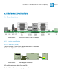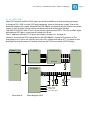
1
STK-MBa35
User's Manual
STK-MBa35 UM 101
01.08.2011
User's Manual l STK-MBa35 UM 101 l © 2011 by TQ-Group
Page i
Table of contents
1.
1.1
1.2
1.3
1.4
1.5
1.6
1.7
1.8
1.9
1.10
2.
3.
3.1
3.1.1
3.1.2
3.1.2.1
3.1.2.2
3.1.2.3
3.1.2.4
3.1.3
4.
4.1
4.1.1
4.1.1.1
4.1.1.2
4.1.1.3
4.1.1.4
4.1.1.5
4.1.1.6
4.1.1.7
4.1.1.8
4.1.1.9
4.1.1.10
4.1.1.11
4.1.1.12
ABOUT THIS MANUAL...................................................................................................................... 1
Copyright............................................................................................................................................. 1
Tips on safety...................................................................................................................................... 1
Symbols and Typographic Conventions.................................................................................... 1
Handling and ESD tips ..................................................................................................................... 2
Registered trademarks..................................................................................................................... 2
Imprint .................................................................................................................................................. 3
Disclaimer ............................................................................................................................................ 3
Copyright and licence expenses................................................................................................... 3
Further applicable documents / presumed knowledge ....................................................... 4
Acronyms and definitions............................................................................................................... 5
BRIEF DESCRIPTION .......................................................................................................................... 7
TECHNICAL DATA.............................................................................................................................. 7
System architecture and system functionality......................................................................... 7
Block diagram..................................................................................................................................... 7
System functionality......................................................................................................................... 7
External interfaces............................................................................................................................. 8
Internal interfaces ............................................................................................................................. 8
User's interfaces................................................................................................................................. 8
System components......................................................................................................................... 8
Technical data mechanics, design ............................................................................................... 8
ELECTRONICS SPECIFICATION....................................................................................................... 9
External interfaces............................................................................................................................. 9
Function specification ..................................................................................................................... 9
Ethernet 1 (X26B)............................................................................................................................... 9
Ethernet 2 (X26A) ............................................................................................................................10
RS485 (X32A) ....................................................................................................................................10
RS232 (X32B).....................................................................................................................................11
CAN 1 / CAN 2 (X1A) .......................................................................................................................12
GPIO (X1B) .........................................................................................................................................13
USB 2.0 Hi-Speed Host (X12-A) ...................................................................................................14
USB 2.0 Hi-Speed OTG (X12-B) ....................................................................................................15
Audio-output right (X27) and left (X28), microphone input (X13)...................................15
Buzzer (N10) ......................................................................................................................................16
SD card (X4).......................................................................................................................................16
Power-IN (X6)....................................................................................................................................16
Page ii
User's Manual l STK-MBa35 UM 101 l © 2011 by TQ-Group
Table of contents
4.1.2
4.1.2.1
4.1.2.2
4.1.2.3
4.1.2.4
4.1.2.5
4.1.2.6
4.1.2.7
4.1.2.8
4.1.2.9
4.1.2.10
4.1.2.11
4.1.2.12
4.1.3
4.1.3.1
4.1.3.2
4.1.3.3
4.1.3.4
4.1.3.5
4.1.3.6
4.1.3.7
4.1.3.8
4.1.3.9
4.1.3.10
4.1.3.11
4.1.3.12
4.2
4.2.1
4.2.1.1
4.2.1.2
4.2.1.3
4.2.1.4
4.2.1.5
4.2.1.6
4.2.1.7
4.2.1.8
4.2.1.9
Electrical characteristics ................................................................................................................17
Ethernet 1 (X26B).............................................................................................................................17
Ethernet 2 (X26A) ............................................................................................................................17
USB 2.0 Hi-Speed Host (X12-A) ...................................................................................................17
USB 2.0 Hi-Speed OTG (X12-B) ....................................................................................................17
RS485 (X32A) ....................................................................................................................................17
RS232 (X32B).....................................................................................................................................17
CAN 1/ CAN 2 (X1A) ........................................................................................................................18
GPIO (X1B) .........................................................................................................................................18
SD card (X4).......................................................................................................................................18
Audio-output right (X27) and left (X28) ...................................................................................19
Microphone input (X13) ................................................................................................................19
Power-IN (X6)....................................................................................................................................19
Plug connectors and pin assignments......................................................................................20
Ethernet 1 (X26B).............................................................................................................................20
Ethernet 2 (X26A) ............................................................................................................................22
RS485 (X32A) ....................................................................................................................................23
RS232 (X32B).....................................................................................................................................24
CAN 1/ CAN 2 (X1A) ........................................................................................................................25
GPIO (X1B) .........................................................................................................................................26
USB 2.0 Hi-Speed Host (X12-A) ...................................................................................................27
USB 2.0 Hi-Speed OTG (X12-B) ....................................................................................................28
Audio-output right (X27) and left (X28) ...................................................................................29
Microphone input (X13) ................................................................................................................30
SD card (X4).......................................................................................................................................31
Power-IN (X6)....................................................................................................................................32
Internal interfaces ...........................................................................................................................33
Function specification ...................................................................................................................35
Module interface (D10)..................................................................................................................35
JTAG (X16) .........................................................................................................................................35
LCD (X22, X23)..................................................................................................................................35
LCD backlight (X21, X24, X5)........................................................................................................36
Touchscreen (X2, X8)......................................................................................................................36
LVDS Display (X9) ............................................................................................................................37
SD card (X25) ....................................................................................................................................38
Power-On (X19)................................................................................................................................38
Starterkit interfaces (X7, X10, X14, X15, X18, X31).................................................................39
User's Manual l STK-MBa35 UM 101 l © 2011 by TQ-Group
Page iii
Table of contents
4.2.2
4.2.2.1
4.2.2.2
4.2.2.2.1
4.2.2.2.2
4.2.2.3
4.2.2.4
4.2.2.5
4.2.2.6
4.2.3
4.2.3.1
4.2.3.2
4.2.3.3
4.2.3.4
4.2.3.5
4.2.3.6
4.2.3.7
4.2.3.8
4.2.3.9
4.2.3.9.1
4.2.3.9.2
4.2.3.9.3
4.2.3.9.4
4.2.3.9.5
4.2.3.9.6
4.3
4.3.1
4.3.2
4.3.3
4.3.4
4.4
4.4.1
4.4.2
4.4.3
Electrical characteristics ................................................................................................................39
LCD (X22, X23)..................................................................................................................................39
LCD backlight (X21, X24, X5)........................................................................................................39
LED driver (X21, X24)......................................................................................................................39
Backlight power supply (X5) ........................................................................................................39
Touchscreen (X2, X8)......................................................................................................................40
LVDS Display (X9) ............................................................................................................................40
SD card (X25) ....................................................................................................................................40
Starterkit interfaces (X7, X10, X14, X15, X18, X31).................................................................40
Plug connector and pins assignment .......................................................................................41
Module interface (D10)..................................................................................................................41
JTAG (X16) .........................................................................................................................................45
LCD (X22, X23)..................................................................................................................................46
LCD backlight (X21, X24, X5)........................................................................................................48
Touchscreen (X2, X8)......................................................................................................................49
LVDS Display (X9) ............................................................................................................................50
SD card (X25) ....................................................................................................................................51
Power-On (X19)................................................................................................................................52
Starterkit interfaces (X7, X10, X14, X15, X18, X31).................................................................52
Starterkit interface (X7)..................................................................................................................53
Starterkit interface (X10) ...............................................................................................................54
Starterkit interface (X14) ...............................................................................................................55
Starterkit interface (X15) ...............................................................................................................56
Starterkit interface (X18) ...............................................................................................................57
Starterkit interface (X31) ...............................................................................................................58
User's interfaces...............................................................................................................................59
Reset button (S2) .............................................................................................................................59
Status-LEDs external (V77)............................................................................................................59
Status-LEDs internal (V22, V24, V25, V46, V78).......................................................................60
DIP switch (S1, S3) ...........................................................................................................................60
System components.......................................................................................................................61
Temperature sensor (D22)............................................................................................................61
I2C address allocation.....................................................................................................................61
Battery.................................................................................................................................................61
Page iv
User's Manual l STK-MBa35 UM 101 l © 2011 by TQ-Group
Table of contents
5.
6.
6.1
6.1.1
6.1.2
6.1.3
7.
7.1
7.2
8.
8.1
8.2
9.
9.1
9.2
9.3
9.4
9.4.1
9.4.2
9.5
9.6
9.7
SOFTWARE SPECIFICATION ..........................................................................................................61
MECHANICS SPECIFICATION........................................................................................................62
Construction .....................................................................................................................................62
PCB outlines STK-MBa35 ...............................................................................................................62
STK-MBa35 top view.......................................................................................................................63
STK-MBa35 bottom view...............................................................................................................64
REQUIREMENTS FOR THE SUPERIOR SYSTEM.........................................................................65
Protection against external effects ............................................................................................65
Thermal management ...................................................................................................................65
SAFETY REQUIREMENTS AND PROTECTIVE REGULATIONS ................................................66
EMC characteristics.........................................................................................................................66
Operational safety and personal security ................................................................................66
CLIMATIC AND OPERATIONAL CONDITIONS ..........................................................................67
Protection against external effects ............................................................................................67
Reliability and product life ...........................................................................................................67
The used displays ............................................................................................................................67
Batteries..............................................................................................................................................67
General notes ...................................................................................................................................67
Lithium battery ................................................................................................................................67
Environment protection................................................................................................................68
RoHS compliance ............................................................................................................................68
WEEE regulation ..............................................................................................................................68
User's Manual l STK-MBa35 UM 101 l © 2011 by TQ-Group
Page v
Table directory
Table 1:
Table 2:
Table 3:
Table 4:
Table 5:
Table 6:
Table 7:
Table 8:
Table 9:
Table 10:
Table 11:
Table 12:
Table 13:
Table 14:
Table 15:
Table 16:
Table 17:
Table 18:
Table 19:
Table 20:
Table 21:
Table 22:
Table 23:
Table 24:
Table 25:
Table 26:
Table 27:
Table 28:
Table 29:
Table 30:
Table 31:
Table 32:
Table 33:
Table 34:
Table 35:
Table 36:
Table 37:
Terms and conventions............................................................................................................. 1
Acronyms....................................................................................................................................... 5
Allocation of the GPIOs............................................................................................................14
Electrical characteristics of the GPIs ....................................................................................18
Electrical characteristics of the GPOs ..................................................................................18
Electrical characteristics of the power supply ..................................................................19
Overview of the function groups of the power supply .................................................19
Plug connector Ethernet 1 (X26B)........................................................................................20
Pin assignment plug connector Ethernet 1 (X26B).........................................................20
Status LEDs Ethernet 1.............................................................................................................21
Plug connector Ethernet 2 (X26A)........................................................................................22
Pin assignment plug connector Ethernet 2 (X26A) ........................................................22
Plug connector RS485 (X32A)................................................................................................23
Pin assignment plug connector RS485 (X32A).................................................................23
Plug connector RS232 (X32B) ................................................................................................24
Pin assignment plug connector RS232 (X32B) .................................................................24
Plug connector CAN 1 and CAN 2 (X1A).............................................................................25
Pin assignment plug connector CAN 1 and CAN 2 (X1A) .............................................25
Plug connector GPIO (X1B).....................................................................................................26
Pin assignment plug connector GPIO (X1B)......................................................................26
Plug connector USB Host (X12-A) ........................................................................................27
Pin assignment plug connector USB Host (X12-A) .........................................................27
Plug connector USB OTG (X12-B) .........................................................................................28
Pin assignment plug connector USB OTG (X12-B) ..........................................................28
Plug connector audio output right (X27) and left (X28)................................................29
Pin assignment plug connector audio output right (X27) and left (X28).................29
Plug connector microphone (X13).......................................................................................30
Pin assignment plug connector microphone (X13)........................................................30
Plug connector external SD card (X4) .................................................................................31
Pin assignment plug connector external SD card (X4) ..................................................31
Plug connector Power-IN (X6)...............................................................................................32
Pin assignment plug connector Power-IN (X6)................................................................32
Allocation of RGB signals on LVDS lines.............................................................................37
Plug connector module interface (D10).............................................................................41
Pin assignment module plug connector (D10-X1) .........................................................42
Pin assignment module plug connector (D10-X2) .........................................................43
Pin assignment module plug connector (D10-X3) .........................................................44
Page vi
User's Manual l STK-MBa35 UM 101 l © 2011 by TQ-Group
Table directory
Table 38:
Table 39:
Table 40:
Table 41:
Table 42:
Table 43:
Table 44:
Table 45:
Table 46:
Table 47:
Table 48:
Table 49:
Table 50:
Table 51:
Table 52:
Table 53:
Table 54:
Table 55:
Table 56:
Table 57:
Table 58:
Table 59:
Table 60:
Table 61:
Table 62:
Table 63:
Table 64:
Table 65:
Table 66:
Table 67:
Table 68:
Table 69:
Table 70:
Table 71:
Table 72:
Table 73:
Table 74:
Plug connector JTAG (X16).....................................................................................................45
Pin assignment plug connector JTAG (X16)......................................................................45
Plug connector LCD (X22, X23) .............................................................................................46
Pin assignment plug connector LCD (X22, X23) ..............................................................46
Plug connector LCD backlight (X21, X24) ..........................................................................48
Pin assignment plug connector LCD backlight (X21, X24)...........................................48
Plug connector LCD backlight (X5)......................................................................................48
Pin assignment plug connector LCD backlight (X5).......................................................48
Plug connector touchscreen (X2).........................................................................................49
Plug connector touchscreen (X8).........................................................................................49
Pin assignment plug connector touchscreen (X2, X8)...................................................49
Plug connector LVDS Display (X9) .......................................................................................50
Pin assignment plug connector LVDS Display (X9) ........................................................50
Plug connector internal SD card (X25)................................................................................51
Pin assignment plug connector internal SD card (X25) ................................................51
Plug connector Power-On (X19)...........................................................................................52
Pin assignment plug connector touchscreen (X2, X8)...................................................52
Plug connector Starterkit interface (X7).............................................................................53
Plug connector pin assignment Starterkit interface (X7)..............................................53
Plug connector Starterkit interface (X10)...........................................................................54
Plug connector pin assignment Starterkit interface (X10) ...........................................54
Plug connector Starterkit interface (X14)...........................................................................55
Plug connector pin assignment Starterkit interface (X14) ...........................................55
Plug connector Starterkit interface (X15)...........................................................................56
Plug connector pin assignment Starterkit interface (X15) ...........................................56
Plug connector Starterkit interface (X18)...........................................................................57
Plug connector pin assignment Starterkit interface (X18) ...........................................57
Plug connector Starterkit interface (X31)...........................................................................58
Plug connector pin assignment Starterkit interface (X31) ...........................................58
Reset button (S2) .......................................................................................................................59
External Status-LEDs (V77)......................................................................................................59
Overview external LEDs...........................................................................................................59
Overview internal LEDs ...........................................................................................................60
DIP switch S1 ..............................................................................................................................60
DIP switch S3 ..............................................................................................................................60
I2C address allocation...............................................................................................................61
Component selection battery RTC.......................................................................................61
User's Manual l STK-MBa35 UM 101 l © 2011 by TQ-Group
Page vii
Illustration directory
Illustration 1:
Illustration 2:
Illustration 3:
Illustration 4:
Illustration 5:
Illustration 6:
Illustration 7:
Illustration 8:
Illustration 9:
Illustration 10:
Illustration 11:
Illustration 12:
Illustration 13:
Illustration 14:
Illustration 15:
Illustration 16:
Illustration 17:
Illustration 18:
Illustration 19:
Illustration 20:
Illustration 21:
Illustration 22:
Illustration 23:
Illustration 24:
Illustration 25:
Illustration 26:
Illustration 27:
Illustration 28:
Illustration 29:
Illustration 30:
Illustration 31:
Illustration 32:
Illustration 33:
Illustration 34:
Illustration 35:
Illustration 36:
Illustration 37:
Illustration 38:
Illustration 39:
Illustration 40:
Block diagram STK-MBa35 ................................................................................................ 7
External interfaces of the STK-MBa35............................................................................ 9
Block diagram Ethernet 1.................................................................................................. 9
Block diagram Ethernet 2................................................................................................10
Block diagram RS485 ........................................................................................................10
Block diagram RS232 ........................................................................................................11
Block diagram CAN............................................................................................................12
Block diagram GPIO ..........................................................................................................13
Block diagram USB Host ..................................................................................................14
Block diagram USB OTG...................................................................................................15
Block diagram audio .........................................................................................................15
Block diagram buzzer .......................................................................................................16
Block diagram external SD card ....................................................................................16
Block diagram Power-IN ..................................................................................................16
Wiring of X26B ....................................................................................................................21
Wiring of X32A....................................................................................................................23
Wiring of X32B ....................................................................................................................24
Wiring of X1A ......................................................................................................................25
Wiring of X1B.......................................................................................................................26
Wiring of X12-A ..................................................................................................................27
Wiring of X12-B...................................................................................................................28
Wiring of X27 / X28............................................................................................................29
Wiring of X13.......................................................................................................................30
Wiring of X4 .........................................................................................................................31
Wiring of X6 .........................................................................................................................32
Component placement top............................................................................................33
Component placement bottom....................................................................................34
Block diagram LCD ............................................................................................................35
Block diagram LCD backlight.........................................................................................36
Block diagram touchscreen ............................................................................................36
Block diagram LVDS Display...........................................................................................37
Block diagram internal SD card .....................................................................................38
Block diagram Power-On.................................................................................................38
Wiring of D10 ......................................................................................................................41
Wiring of X21, X24 .............................................................................................................48
Wiring of X25.......................................................................................................................51
Block diagram LED.............................................................................................................59
PCB outlines STK-MBa35..................................................................................................62
Top view ...............................................................................................................................63
Bottom view ........................................................................................................................64
Page viii
User's Manual l STK-MBa35 UM 101 l © 2011 by TQ-Group
Revision history
Rev.:
Date:
Name:
100
14.04.2011
Petz
101
01.08.2011
Petz
Pos.:
Modification:
Document created
Illustration 2
Table 39
7.1.1
7.1.2
8.1.1
8.1.2
Replaced
Remarks corrected
7.1
7.2
8.1
8.2
Typo
User's Manual l STK-MBa35 UM 101 l © 2011 by TQ-Group
Page 1
1. ABOUT THIS MANUAL
1.1 Copyright
Copyright protected © 2011 by TQ-Components GmbH.
This User’s Manual may not be copied, reproduced, translated, changed or distributed,
completely or partially in electronic, machine readable, or in any other form without the written
consent of TQ-Components GmbH.
1.2 Tips on safety
Improper or incorrect handling of the product can substantially reduce its life span.
1.3 Symbols and Typographic Conventions
Table 1:
Symbol /
Visual Cue
Terms and conventions
Meaning
This symbol represents the handling of electrostatic-sensitive modules and /
or components. These components are often damaged / destroyed by the
transmission of a voltage higher than about 50 V. A human body usually only
experiences electrostatic discharges above approximately 3,000 V.
This symbol indicates the possible use of voltages higher than 24 V. Please
note the relevant statutory regulations in this regard. Non-compliance with
these regulations can lead to serious damage to your health and also cause
damage / destruction of the component.
This symbol indicates a possible source of danger. Acting against the
procedure described can lead to possible damage to your health and / or
cause damage / destruction of the material used.
This symbol represents important details or aspects for working with TQproducts.
Command
A font with fixed-width is used to denote commands, file names, or menu
items.
Page 2
User's Manual l STK-MBa35 UM 101 l © 2011 by TQ-Group
1.4 Handling and ESD tips
General handling of your TQ-products
The TQ-product may only be used and serviced by certified personnel who
have taken note of the information, the safety regulations in this document
and all related rules and regulations.
A general rule is: do not touch the TQ-product during operation. This is
especially important when switching on, changing jumper settings or
connecting other devices without ensuring beforehand that the power supply
of the system has been switched off.
Violation of this guideline may result in damage / destruction of the module
and be dangerous to your health.
Improper handling of your TQ-product would render the guarantee invalid.
Proper ESD handling
The electronic components of your TQ-product are sensitive to electrostatic
discharge (ESD).
Always wear antistatic clothing, use ESD-safe tools, packing materials etc., and
operate your TQ-product in an ESD-safe environment. Especially when you
switch modules on, change jumper settings, or connect other devices.
1.5 Registered trademarks
TQ-Components GmbH aims to adhere to the copyrights of all the used graphics and texts in all
publications and strives to use original or license-free graphics and texts.
All the brand names and trademarks mentioned in the publication, including those protected by
a third party, unless specified otherwise in writing, are subjected to the specifications of the
current copyright laws and the proprietary laws of the present registered proprietor without any
limitation. One should conclude that brands and trademarks are protected through the rights of
a third party.
User's Manual l STK-MBa35 UM 101 l © 2011 by TQ-Group
Page 3
1.6 Imprint
TQ-Components GmbH
Gut Delling, Mühlstraße 2
82229 Seefeld
Tel:
+49 (0)8153 9308–0
Fax:
+49 (0)8153 9308–134
Email: [email protected]
Web:
http://www.tq-group.com/
1.7 Disclaimer
TQ-Components GmbH does not guarantee that the information in this manual is up-to-date,
correct, complete or of good quality. Nor does TQ-Components assume guarantee for further
usage of the information. Liability claims against TQ-Components GmbH, referring to material or
non-material related damages, caused due to usage or non-usage of the information given in the
manual, or caused due to usage of erroneous or incomplete information, are exempted, as long
as there is no proven, intentional or negligent fault of TQ-Components GmbH.
TQ-Components GmbH explicitly reserves the rights to change or add to the contents of this
manual or parts of it without special notification.
1.8 Copyright and licence expenses
The drivers and utilities for the used components as well as the BIOS are subject to the
copyrights of the respective manufacturers. The licence conditions of the respective
manufacturer are to be adhered to.
Bootloader-licence expenses are paid by TQ and are included in the price.
Licence expenses for the operating system and applications are not taken into consideration and
must be separately calculated / declared.
Page 4
User's Manual l STK-MBa35 UM 101 l © 2011 by TQ-Group
1.9 Further applicable documents / presumed knowledge
•
Specifications and manual of the used modules:
These documents describe the service, functionality and special characteristics of the
used module (incl. BIOS).
•
Specifications of the used components:
The manufacturer's specifications of the used components, for example Compact-Flash
cards, are to be taken note of. They contain, if applicable, additional information that
must be taken note of for safe and reliable operation. These documents are stored at TQ.
•
Chip errata:
It is the user's responsibility to make sure all errata published by the manufacturer of
each component are taken note of. The manufacturer’s advice should be followed.
•
Software behaviour:
No warranty can be given, nor responsibility taken for any unexpected software
behaviour due to deficient components.
•
General expertise:
Expertise in electrical engineering / computer engineering is required for the installation
and the use of the device.
User's Manual l STK-MBa35 UM 101 l © 2011 by TQ-Group
1.10 Acronyms and definitions
The following acronyms and abbreviations are used in this document:
Table 2:
Acronyms
Acronym
Meaning
AC
AGND
ARM®
CAN
CPU
DC
DCE
DGND
DIN
DIP
DTE
EEPROM
EMC
EMMC
EN
FET
FFC
FPC
FR-4
GND
GPI
GPIO
GPO
HD-D-sub
I/O
I/P
IEEE
IP00
I2C
JTAG
LCD
Alternating Current
Analog Ground
Advanced RISC Machine
Controller Area Network
Central Processing Unit
Direct Current
Data Communication Equipment (e.g. modem)
Digital Ground
Deutsche Industrie Norm
Dual In-line Package
Data Terminal Equipment (e.g. PC)
Electrically Erasable Programmable Read-only Memory
Electromagnetic Compatibility
embedded MultiMediaCard (Flash)
Europäische Norm (European Standards)
Field Effect Transistor
Flat Flex Cable
Flexible Printed Circuit
Flame Retardant-4
Ground
General Purpose Input
General Purpose Input/Output
General Purpose Output
High Density D-sub
Input/Output
Input/Power
Institute of Electrical and Electronics Engineers
Ingress Protection 00
Inter-Integrated Circuit
Joint Test Action Group
Liquid Crystal Display
Page 5
Page 6
User's Manual l STK-MBa35 UM 101 l © 2011 by TQ-Group
Acronym
Meaning
LED
LVDS
MIC
MII
MMC
MOZI
NC
OTG
PCB
PHY
PMIC
PWM
RAM
RCA
RFU
RGB
RJ
RoHS
RS232
RTC
SD
SDHC
SPI
SPS
THD+N
UART
UN
USB
VGA
WEEE
WEIM
WP
Light Emitting Diode
Low Voltage Differential Signal
Microphone
Media-Independent Interface
Multimedia Card
Module extractor (Modulzieher)
Not Connected
On-The-Go
Printed Circuit Board
Physical (Interface)
Power Management IC
Pulse Width Modulation
Random Access Memory
Radio Corporation of America
Reserved for Future Use
Red Green Blue
Registered Jack
Restriction of (the use of certain) Hazardous Substances
Recommended Standard (serial interface)
Real-Time Clock
Secure Digital
Secure Digital High Capacity
Serial Peripheral Interface
Speicherprogrammierbare Steuerung Ö Programmable Logic Controller (PLC)
Total Harmonic Distortion + Noise
Universal Asynchronous Receiver/Transmitter
United Nations
Universal Serial Bus
Video Graphics Array (640 × 480)
Waste Electrical and Electronic Equipment
Wireless External Interface Module
Write-Protection
Page 7
User's Manual l STK-MBa35 UM 101 l © 2011 by TQ-Group
2. BRIEF DESCRIPTION
The STK-MBa35 is designed to be driven by TQ modules based on the Freescale ARM CPU
MCIMX35 (i.MX35). In combination with a module and a display with touchscreen it offers PC
core functionalities and standard interfaces.
By using the functionalities of the Starterkit STK-MBa35 this main board forms together with the
TQMa35 a modular system to develop own product ideas.
3. TECHNICAL DATA
3.1 System architecture and system functionality
3.1.1 Block diagram
external
SD card
Microphone
3.5 mm phone jack
HP / Line out
Buzzer
2 x Cinch (stereo)
Audio codec
SGTL5000
LVDS
connector
LED
backlight
Ethernet 2
RJ45
LVDS
transmitter
Backlight
driver
Ethernet
controller
SN75LVDS83B
LT3518
LAN9115
LCD
SSI4
WEIM
type A
LCD bus
USB OTG
SD1
type A
PWM
USB Host
120-pin plug connector
80-pin plug connector
Tyco 5177986-3
Debug header
Tyco 5177986-5
TQMa35
120-pin plug connector
CAN
transceiver
Ethernet
transceiver
RS232
transceiver
RS485
transceiver
MCP2551
MCP2551
78Q2133
SP3222E
SP491E
I2C 1
PCA9554
I2C
expander
PCA9554
High-Side
driver
VN808CM-E
2 x CAN
Ethernet 1
RS232
RS485
24 V GPIO
D-Sub 9-pin
RJ45
D-Sub 9-pin
D-Sub 9-pin
D-Sub 15-pin
Illustration 1:
Touch
controller
Temperature
sensor
ADS7846
LM75CIMM-3
Touch
RTC backup
battery
SD3
CAN
transceiver
I2C
expander
VBAT
Opto
coupler
I2C 1
Opto
coupler
SPI 2
Opto
coupler
I2C 1
UART 2
UART 3
ETH MII
CAN 1
CAN 2
Tyco 5177986-5
Internal
SD card
Block diagram STK-MBa35
3.1.2 System functionality
The interfaces and system components listed in the following are implemented on the STKMBa35. Due to the fact that the STK-MBa35 can be installed in a casing the interfaces are divided
into external and internal interfaces.
Page 8
User's Manual l STK-MBa35 UM 101 l © 2011 by TQ-Group
3.1.2.1 External interfaces
•
•
•
•
•
•
•
•
•
•
•
2 × Ethernet 10/100 Mbit
1 × RS485
1 × RS232
2 × CAN
1 × USB 2.0 Hi Speed Host interface
1 × USB 2.0 Hi Speed On-The-Go device interface
1 × GPIO (8 × OUT / 4 × IN)
1 × SD card
2 × Audio output
1 × Microphone input
1 × Power supply
3.1.2.2 Internal interfaces
•
•
•
•
•
•
•
•
•
1 × TQMa35
1 × JTAG
2 × LCD (model dependent)
2 × LCD backlight (model dependent)
2 × Touchscreen (model dependent)
1 × LCD via LVDS (optional)
1 × SD card (optional)
1 × Power-On button
5 × headers and 1 × power supply (Starterkit function / optional)
3.1.2.3 User's interfaces
•
•
•
•
1 × Reset button
3 × Status LEDs (external)
5 × Status LEDs (internal)
2 × DIP switch
3.1.2.4 System components
•
•
•
•
•
Backup battery
Buzzer
Temperature sensor
Power supply
Voltage supervision and reset concept
3.1.3 Technical data mechanics, design
Dimensions PCB (W × D × H):
Overall dimensions (W × D × H):
Weight:
175 × 120 × 2 mm3
175 × 130 × 32 mm3 (app.)
261 g
User's Manual l STK-MBa35 UM 101 l © 2011 by TQ-Group
4. ELECTRONICS SPECIFICATION
4.1 External interfaces
Illustration 2:
External interfaces of the STK-MBa35
4.1.1 Function specification
4.1.1.1 Ethernet 1 (X26B)
The MII interface of the TQMa35 drives the Ethernet 1 interface.
The Teridian78Q2133 is used as PHY.
TQMa35 - X1
78Q2133
FEC_TXDN
TPI
MII
GPIO2_25
TQM_RESET_OUT#
Illustration 3:
RJ45
TPO
FEC_RXDN
INTR
RSTN#
Block diagram Ethernet 1
LED configuration see Table 9 on page 20.
Further LED configurations are programmable.
LED0
LED
LED1
LED
Page 9
Page 10
User's Manual l STK-MBa35 UM 101 l © 2011 by TQ-Group
4.1.1.2 Ethernet 2 (X26A)
The Ethernet 2 interface is implemented by using the SMSC WEIM-PHY LAN9115.
This interface is only available if the TQMa35 is equipped with plug connector X3.
TQMa35 - X3
LAN9115
ADDR[7:1]
TPO
A[7:1]
OE#_3V3
RD#
RW#_3V3
WR#
CS#1_3V3
CS#
GPIO3_3
IRQ
GPIO3_4
PME
TQM_RESET_OUT#
Illustration 4:
RJ45
D[15:0]
D[15:0]
TPI
LED1#
LED2#
LED
LED
LED3#
LED
RESET#
Block diagram Ethernet 2
LED configuration see Table 12 on page 22.
4.1.1.3 RS485 (X32A)
The UART2 of the TQMa35 drives the RS485 interface of the STK-MBa35. The optocouplers Avago
HCPL0631 and HCPL0601 are used for galvanic separation. The Recom RSS-0505/HP serves as the
power supply for the galvanically separated part of the RS485 interface.
The Exar SP491EEN-L is used as RS485 transceiver.
galvanic
separation
SP491E
UART2_CTS#
UART2_TxD
HCPL0631
DE
DI
UART2_RxD
HCPL0601
RO
S3-4
D-Sub 9
120 R
TQMa35 - X1
Y/Z
n.a.
RE#
120 R
A/B
RSS-0505/HP
S3-3
Illustration 5:
Block diagram RS485
The RS485 signals can be terminated with 120 Ω with either DIP switch S3 or cable-sided by
bridging pins 8 / 9 (RxD) and 1 / 7 (TxD). Details can be found in Table 72 on page 60.
User's Manual l STK-MBa35 UM 101 l © 2011 by TQ-Group
Page 11
4.1.1.4 RS232 (X32B)
The UART3 interface of the TQMa35 drives the RS232 interface of the STK-MBa35 by default.
The Exar SP3222EEA-L is used as a driver. The RS232 interface driver on the TQMa35 can be used
as an alternative. This uses UART1 of the TQMa35. It is however not recommended due to EMC
reasons.
TQMa35 - X1
RS232_TX
n.a.
RS232_RX
n.a.
SP3222E
Illustration 6:
D-Sub 9
UART3_TxD
T1IN
T1OUT
TxD
UART3_CTS
T2IN
T2OUT
RTS
UART3_RxD
R1OUT
R1IN
RxD
UART3_RTS
R2OUT
R2IN
CTS
Block diagram RS232
The CPU i.MX35 on the TQMa35 is designed as data communication equipment (DCE).
The signals RTS and CTS do therefore not behave as in data terminal equipment (DTE, e.g., PC).
The signal UART3_RTS of the TQMa35 is an input, the signal UART3_CTS of the TQMa35 is an
output.
To compensate for this behaviour of the i.MX35, the signals RTS and CTS are crossed on the STKMBa35:
•
•
the CTS signal coming from an external source via (X32_8B) is routed as signal
UART3_RTS on the STK-MBa35 to pin X1_108 of the TQMa35
the RTS signal going to an external receiver via (X32_7B) comes as signal UART3_CTS
on the STK-MBa35 from pin X1_109 of the TQMa35
Page 12
User's Manual l STK-MBa35 UM 101 l © 2011 by TQ-Group
4.1.1.5 CAN 1 / CAN 2 (X1A)
The two CAN ports of the TQMa35 directly drive both CAN interfaces on the STK-MBa35.
Optocouplers of type Avago HCPL0601 are used for galvanic separation. The Recom RTS-0505/P
serves as the power supply for the galvanically separated part of the CAN interface.
Microchip MCP2551T-I/SN are used as CAN transceivers.
galvanic
separation
MCP2551
CAN[1,2]TxD
HCPL0601
TxD
CAN[1,2]RxD
HCPL0601
RxD
S1 - 1/2
D-Sub 9
120 R
TQMa35 - X1
CANH
CANL
RTS-0505/P
Illustration 7:
Block diagram CAN
The CAN signals can be terminated with 120 Ω by using DIP switch S1 (see Table 71 on page 60).
User's Manual l STK-MBa35 UM 101 l © 2011 by TQ-Group
Page 13
4.1.1.6 GPIO (X1B)
Eight GPIO outputs and four GPIO inputs are made available at an external plug connector.
A voltage of 24 V ±20 % at the GPIO plug connector serves as the power supply. Due to the
placement option the supply voltage of the STK-MBa35 can alternatively be used as the power
supply. In this case the user has to ensure the correct level of the input voltage.
Two NXP (PCA9554D) 8 bit I2C bus I/O port circuits generate the GPIOs. This circuit offers eight
bidirectional GPIO ports, which can drive and sink 10 mA.
The I2C addresses of both I2C I/O ports are listed in section 4.4.1 on page 61.
The basic circuit of the GPIO connection on the STK-MBa35 is shown in Illustration 8. The
remaining four I/O ports are used for two user-LEDs (yellow and red) at V77, to switch on the
backlight via plug connector X5 and to switch on the LVDS transmitter (LVDS Display).
TQMa35 - X1
PCA9554
VN808CM-E
D-Sub 15
I2C 1
STATUS
GPIO1_12
PCA9554
10 nF
4k7
10 k
USER_LED1
USER_LED2
LD_BKL_ON
LCD_LVDS_ENA
Illustration 8:
Block diagram GPIO
100 pF
Page 14
User's Manual l STK-MBa35 UM 101 l © 2011 by TQ-Group
Table 3:
Allocation of the GPIOs
Signal
I2C base address
GPO1
GPO2
GPO3
GPO4
GPO5
GPO6
GPO7
GPO8
GPI1
GPI2
GPI3
GPI4
USER_LED1
USER_LED2
LD_BKL_ON
LCD_LVDS-ENA
I/O port
Direction
IO0
IO1
IO2
IO3
IO4
IO5
IO6
IO7
IO0
IO1
IO2
IO3
IO4
IO5
IO6
IO7
0x20
0x21
O
O
O
O
O
O
O
O
I
I
I
I
O
O
O
O
4.1.1.7 USB 2.0 Hi-Speed Host (X12-A)
The USB host interface of the TQMa35 is routed directly to the USB-A jack X12-A, including the
protection circuit. The over-current protection is implemented with a Texas Instruments
TPS2042B.
TQMa35 - X2
USB-A
USBHS_UDM/UDP
D+ / D-
TPS2042B
USBHS_PSW#
EN1#
USBHS_OC
OC1#
OUT1
LED
Illustration 9:
Block diagram USB Host
1k
USBHS_VBUS
VBUS
User's Manual l STK-MBa35 UM 101 l © 2011 by TQ-Group
Page 15
4.1.1.8 USB 2.0 Hi-Speed OTG (X12-B)
The USB OTG interface is configured as the host by default and cannot be connected to a PC as
device.
To offer OTG functionality it is possible to provide a USB-Mini-AB jack or Mini-B by a placement
option.
However, as a result the USB 2.0 Hi Speed interface falls away.
TQMa35 - X2
USB-A
USBOTG_UDM/UDP
D+ / D-
USBOTG_VBUS
EN2#
USBOTG_OC
OC2#
1k
TPS2042B
USBOTG_PSW#
OUT2
VBUS
n.a.
LED
USBOTG_UID
USB-mini-AB
0R
D+ / DVBUS
ID
Illustration 10:
Block diagram USB OTG
4.1.1.9 Audio-output right (X27) and left (X28), microphone input (X13)
The audio-functionality is implemented with a Freescale SGTL5000 on the STK-MBa35.
TQMa35 - X1/X2
I2S
I2C1
CLKO
SGTL5000
I2S
CTRL
HP_L
HP_R
Cinch
SYS_MCLK
MIC
Illustration 11:
Cinch
HP_VGND
Block diagram audio
The SGTL5000 can be accessed via I2C base address 0x0A.
100 nF
Phone
jack
Page 16
User's Manual l STK-MBa35 UM 101 l © 2011 by TQ-Group
4.1.1.10 Buzzer (N10)
The PWM output of the TQMa35 controls the buzzer.
TQMa35 - X2
Buzzer
PWM
Illustration 12:
Block diagram buzzer
4.1.1.11 SD card (X4)
The external SD card is connected to the SD1 bus of the TQMa35. Card-Detect and Write-Protect
of the card are connected to GPIOs of the TQMa35.
TQMa35 - X1, X2
SD slot
SD
SD1
Illustration 13:
GPIO2_0
CD#
GPIO2_7
WP#
Block diagram external SD card
4.1.1.12 Power-IN (X6)
For protective and EMC reasons the supply input of the STK-MBa35 is designed very robustly.
Plug
connector
24 V
Fuse
3.5 A, F
Illustration 14:
Overvoltage
protection
30 V
Filter
Block diagram Power-IN
Reverse
polarity
protection
Overvoltage
protection
30 V
Filter
Switching
regulator
User's Manual l STK-MBa35 UM 101 l © 2011 by TQ-Group
4.1.2 Electrical characteristics
4.1.2.1 Ethernet 1 (X26B)
Type of media:
Interface on module:
Status LEDs:
Signal characteristic:
10/100 Mbit
MII interface (controller on the module TQMa35)
See Table 9 on page 20
Compatible with the IEEE-802.3 standard
4.1.2.2 Ethernet 2 (X26A)
Type of media:
Interface on module:
Status LEDs:
Signal characteristic:
10/100 Mbit
External memory bus (WEIM) / controller on the STK-MBa35
See Table 12 on page 22
Compatible with the IEEE-802.3 standard
4.1.2.3 USB 2.0 Hi-Speed Host (X12-A)
Type of media:
Interface on module:
Signal characteristic:
ESD protection:
USB 2.0 Hi-Speed, 5 V bus voltage (limited to 500 mA)
USB Host physical
Compatible with the Universal Serial Bus Specification Rev. 2.0
±15 kV human body model
4.1.2.4 USB 2.0 Hi-Speed OTG (X12-B)
Type of media:
Interface on module:
Signal characteristic:
ESD protection:
USB 2.0 OTG Hi-Speed, 5 V bus voltage (limited to 500 mA)
USB OTG physical (only OTG / cannot be used as device)
Compatible with the Universal Serial Bus Specification Rev. 2.0
±15 kV human body model
4.1.2.5 RS485 (X32A)
Transfer rate:
Interface on module:
Handshake:
Signal characteristic:
ESD protection:
Up to 4 Mbit/s (full-duplex)
UART2
Used for clearing the transmission direction
Compatible with the EIA/TIA-485 standard / galvanically separated
±15 kV human body model
4.1.2.6 RS232 (X32B)
Transfer rate:
Interface on module:
Handshake:
Signal characteristic:
ESD protection:
Up to 120 Kbit/s
UART3 resp. RS232 (optional)
RTS/CTS (via UART3) resp. none (via RS232 from module / optional)
Compatible with the EIA/TIA-232 standard
±15 kV human body model
Page 17
Page 18
User's Manual l STK-MBa35 UM 101 l © 2011 by TQ-Group
4.1.2.7 CAN 1/ CAN 2 (X1A)
Transfer rate:
Interface on module:
Signal characteristic:
Up to 1 Mbit/s
CAN1 resp. CAN2
Compatible with the ISO-11898 standard (CAN 2.0B) /
galvanically separated
6 kV human body model
ESD protection:
4.1.2.8 GPIO (X1B)
Type of media:
Interface on module:
Signal characteristic:
ESD protection:
Table 4:
24 V GPIOs (according to the SPS standard)
I2C1
See Table 4 / not galvanically separated
600 W pulse power (10 / 1 ms, 0.01 % duty cycle)
Electrical characteristics of the GPIs
Parameter
Min.
Input frequency (hardware limitation)
Input voltage VIN
Input current (VIN = 28 V)
Positive trigger level (LOW-to-HIGH)
Negative trigger level (HIGH-to-LOW)
Typ.
0
4.4
2.2
5.3
3.1
Max.
15
28
2.5
7.5
5.3
Unit
kHz
V
mA
V
V
Depending on the operating system and its workload the maximum input frequency can be significantly
lower than the value specified by the hardware.
Table 5:
Electrical characteristics of the GPOs
Parameter
Min.
Output frequency
Supply voltage (VCC24V_EX)
Output voltage (depending on RLoad)
Load resistance RLoad
Load inductance (VCC24V_EX = 24 V, RLoad = 48 Ω)
Output current of a single output
Output current of all outputs together
Short circuit current (VCC24V_EX = 24 V, RLoad = 10 mΩ)
12
Typ.
24
<VCC24V_EX
Max.
3
30
48
0.7
2
700
5
1.7
Unit
kHz
V
V
Ω
H
mA
A
A
4.1.2.9 SD card (X4)
Type of media:
Interface on module:
Signal characteristic:
SD / SDHC card
SD 4-bit
Compatible with the SD Host Controller Standard Specification version 2.0
Support for high capacity SD memory cards
Page 19
User's Manual l STK-MBa35 UM 101 l © 2011 by TQ-Group
4.1.2.10 Audio-output right (X27) and left (X28)
SNR (–60 dB Input):
THD+N:
Load:
Power output:
98 dB
–86 dB
16 Ω
58 mW
4.1.2.11 Microphone input (X13)
Input:
Gain:
Mono
Programmable (0, +20, +30, +40 dB)
4.1.2.12 Power-IN (X6)
Table 6:
Electrical characteristics of the power supply
Parameter
Min.
Input voltage
Input current
Power consumption
Rated current of the fuse
Voltage drop in the fuse
Melting time of the fuse (t < 10 ms)
Melting time of the fuse (I = 10 ∗ IN)
15
Typ.
Max.
24
190
4.56
3.5
30
0.13
3.9
3.3
Unit
V
mA
W
A
V
A2s
A2s
The specified standard power supply for the STK-MBa35 is the following:
•
IPCX86MM NT REV. 100 Ö 18 V (max. 3.9 A)
With the abovementioned power supply the low voltage directives according to EN 60950 are
met. In the case where another power supply is used or if the device is supplied from a 24 V
power grid, it is the customer’s responsibility to make sure the specified maximum ratings and
standards are met.
Table 7:
Overview of the function groups of the power supply
Parameter
Min.
Reverse voltage protection
Yes, actively via serial FET (max. 30 V for both polarities allowed)
Yes, voltage limitation to 30 V.
With lasting excess voltage the assembly can be damaged!
Yes. Passive over current protection by soldered ceramic fuse.
Integrated filters for the power supply input.
Excess voltage protection
Short circuit protection
Filter
Page 20
User's Manual l STK-MBa35 UM 101 l © 2011 by TQ-Group
4.1.3 Plug connectors and pin assignments
4.1.3.1 Ethernet 1 (X26B)
Table 8:
Plug connector Ethernet 1 (X26B)
Manufacturer
Description
Tyco, 6368011-3
•
•
•
•
Type: 2 × RJ45 jack
Eight contacts each
LEDs: green and yellow
–40 °C to +80 °C
The following table shows the configuration of the plug connector for Ethernet 1.
Table 9:
Pin
1
2
3
4
5
6
7
8
M
LED1
LED2
Pin assignment plug connector Ethernet 1 (X26B)
Signal
TX+
TX–
RX+
Termplane
Termplane
RX–
Termplane
Termplane
DGND
Link_Activity
Speed_Indicator
Type
O
O
I
–
–
I
–
–
P
–
–
Remark
Galvanically separated
Galvanically separated
Galvanically separated
75 Ω, AC coupled to DGND
Connected to pin 4
Galvanically separated
75 Ω, AC coupled to DGND
Connected to pin 7
Ground housing
See Table 10 on page 21
See Table 10 on page 21
User's Manual l STK-MBa35 UM 101 l © 2011 by TQ-Group
Page 21
Two LEDs are used for diagnosis of the interface. The LEDs are visible from the outside and can
be configured via the register MR23 of the Ethernet transceiver.
Table 10:
Register MR23
0000
0001
0010
0011
0100
0101
0110
0111
1000
Status LEDs Ethernet 1
Status display
Remark
Link OK
RX/TX activity
TX activity
RX activity
Collision
100 BASE-TX mode
10 BASE-T mode
Full-duplex
LED on: Link OK
Blinking: RX/TX activity
Standard for yellow LED
Standard for green LED
Illustration 15:
Wiring of X26B
Page 22
User's Manual l STK-MBa35 UM 101 l © 2011 by TQ-Group
4.1.3.2 Ethernet 2 (X26A)
Table 11:
Plug connector Ethernet 2 (X26A)
Manufacturer
Description
Tyco, 6368011-3
•
•
•
•
Type: 2 × RJ45 jack
Eight contacts each
LEDs: green and yellow
–40 °C to +80 °C
Two LEDs are used for diagnosis of the interface. The LEDs are visible from the outside and have
predefined functions.
The following table shows the configuration of the plug connector for Ethernet 2.
Table 12:
Pin
Pin assignment plug connector Ethernet 2 (X26A)
Signal
Type
1
2
3
4
5
6
7
8
M
TX+
TX–
RX+
Termination
Termination
RX–
Termination
Termination
DGND
O
O
I
–
–
I
–
–
P
LED1
Link_Activity
–
LED2
Speed_Indicator
–
LED3
V78
Duplex_Indicator
–
Remark
Galvanically separated
Galvanically separated
Galvanically separated
75 Ω, AC coupled to DGND
75 Ω, AC coupled to DGND
Ethernet 1; galvanically separated
75 Ω, AC coupled to DGND
75 Ω, AC coupled to DGND
Ground housing
Link activity (green LED)
LED on:
Valid link and network cable plugged in
LED off:
No valid link, network cable not plugged in
Blinking:
Packet transmission (transmission or reception)
Speed indicator (yellow LED)
LED on:
100 Mbit/s, disconnected resp. autonegotiation
LED off:
10 Mbit/s
Duplex indicator (green LED)
LED on:
Full-duplex
LED off:
Half-duplex
LED V78 is visible from outside
(positioned on the right hand side of the RJ45 jack)
Wiring of X26A see Illustration 15 on page 21.
User's Manual l STK-MBa35 UM 101 l © 2011 by TQ-Group
Page 23
4.1.3.3 RS485 (X32A)
Table 13:
Plug connector RS485 (X32A)
Manufacturer
Description
Yamaichi, DDP-011S1
•
•
•
Dual standard D-sub connector
9-pin each
–55 °C to +105 °C
The following table shows the configuration of the plug connector for RS485.
Table 14:
Pin
1
2
3
4
5
6
7
8
9
M
Pin assignment plug connector RS485 (X32A)
Signal
Type
Remark
RS485_Y
NC
NC
RS485_A
GND_S2
RS485_Z
120R_TX
120R_RX
RS485_B
DGND
O
–
–
I
P
O
–
–
I
P
Non inverted output / galvanically separated
Not connected
Not connected
Non inverted input / galvanically separated
Ground / galvanically separated
Inverted output / galvanically separated
Bridge to pin 1 for 120 Ω termination
Bridge to pin 9 for 120 Ω termination
Inverted input / galvanically separated
Ground housing
Illustration 16:
Wiring of X32A
Attention: Destruction or malfunction!
Due to three physically identical 9-pin D-sub connectors there is the danger of
confusion between RS232, RS485 and CAN.
The exact arrangement of the interfaces is shown in Illustration 2 on page 9.
Page 24
User's Manual l STK-MBa35 UM 101 l © 2011 by TQ-Group
4.1.3.4 RS232 (X32B)
Table 15:
Plug connector RS232 (X32B)
Manufacturer
Description
Yamaichi, DDP-011S1
•
•
•
Dual Standard D-sub connector
9-pin each
–55 °C to +105 °C
The following table shows the configuration of the plug connector for RS232.
Table 16:
Pin
1
2
3
4
5
6
7
8
9
M
Pin assignment plug connector RS232 (X32B)
Signal
NC
RS232_RxD
RS232_TxD
NC
DGND
NC
RS232_RTS
RS232_CTS
NC
DGND
Illustration 17:
Type
–
I
O
–
P
–
O
I
–
P
Remark
Not connected
Received Data
Transmitted Data
Not connected
Ground
Not connected
Request To Send
Clear To Send
Not connected
Ground
Wiring of X32B
Attention: Destruction or malfunction!
Due to three physically identical 9-pin D-sub connectors there is the danger of
confusion between RS232, RS485 and CAN.
The exact arrangement of the interfaces is shown in Illustration 2 on page 9.
User's Manual l STK-MBa35 UM 101 l © 2011 by TQ-Group
Page 25
4.1.3.5 CAN 1/ CAN 2 (X1A)
Table 17:
Plug connector CAN 1 and CAN 2 (X1A)
Manufacturer
Description
Yamaichi, DDPXR-E9P/E15S-C4N-CT
•
•
•
•
Dual Standard D-sub connector / jack
Top: 9-pin jack
Bottom: 15-pin jack
–55 °C to +105 °C
The following table shows the configuration of the plug connector for both CAN interfaces.
Table 18:
Pin
1
2
3
4
5
6
7
8
9
M
Pin assignment plug connector CAN 1 and CAN 2 (X1A)
Signal
CANL_2
CANL_1
GND_CAN
CANH_2
NC
NC
CANH_1
NC
NC
DGND
Illustration 18:
Type
I/O
I/O
P
I/O
–
–
I/O
–
–
P
Remark
CAN Low-Level I/O of CAN 2 / galvanically separated
CAN Low-Level I/O of CAN 1 / galvanically separated
Ground / galvanically separated
CAN High-Level I/O of CAN 2 / galvanically separated
Not connected
Not connected
CAN High-Level I/O of CAN 1 / galvanically separated
Not connected
Not connected
Ground housing
Wiring of X1A
Attention: Destruction or malfunction!
Due to three physically identical 9-pin D-sub connectors there is the danger of
confusion between RS232, RS485 and CAN.
The exact arrangement of the interfaces is shown in Illustration 2 on page 9.
Page 26
User's Manual l STK-MBa35 UM 101 l © 2011 by TQ-Group
4.1.3.6 GPIO (X1B)
Table 19:
Plug connector GPIO (X1B)
Manufacturer
Description
Yamaichi, DDPXR-E9P/E15S-C4N-CT
•
•
•
•
Dual Standard D-sub connector / jack
Top: connector 9-pin
Bottom: jack 15-pin
–55 °C to +105 °C
The following table shows the configuration of the plug connector for the GPIOs.
Table 20:
Pin
1
2
3
4
5
6
7
8
9
10
11
12
13
14
15
M
Pin assignment plug connector GPIO (X1B)
Signal
IN0
IN1
IN2
IN3
GND_EX
VCC24V_EX
GND_EX
OUT7
OUT6
OUT5
OUT4
OUT3
OUT2
OUT1
OUT0
DGND
Illustration 19:
Type
I
I
I
I
P
P
P
O
O
O
O
O
O
O
O
P
Remark
Input 0
Input 1
Input 2
Input 3
Ground
Supply input for the outputs
Ground
Output 7
Output 6
Output 5
Output 4
Output 3
Output 2
Output 1
Output 0
Ground housing
Wiring of X1B
Attention: Destruction or malfunction!
The 15-pin HD-D-sub connector for GPIO (X1B) looks like a VGA-monitor output.
No monitor may be connected there!
User's Manual l STK-MBa35 UM 101 l © 2011 by TQ-Group
Page 27
4.1.3.7 USB 2.0 Hi-Speed Host (X12-A)
Table 21:
Plug connector USB Host (X12-A)
Manufacturer
Description
Yamaichi, USB-A-002A
•
•
•
•
Dual USB jack, type A
UN = 30 V AC (rms) / IN = 1 A
Umax = 500 V AC for 1 minute
–55 °C to +85 °C
The following table shows the configuration of the plug connector for the USB Host interface.
Table 22:
Pin
1
2
3
4
M
Pin assignment plug connector USB Host (X12-A)
Signal
VBUS
DM
DP
DGND
DGND
Illustration 20:
Type
P
I/O
I/O
P
P
Remark
5 V supply (current limitation to 0.5 A) / 100 μF
Negative differential data line
Positive differential data line
Ground
Ground housing
Wiring of X12-A
Page 28
User's Manual l STK-MBa35 UM 101 l © 2011 by TQ-Group
4.1.3.8 USB 2.0 Hi-Speed OTG (X12-B)
Table 23:
Plug connector USB OTG (X12-B)
Manufacturer
Description
Yamaichi, USB-A-002A
•
•
•
•
Dual USB jack, type A
UN = 30 V AC (rms) / IN = 1 A
Umax = 500 V AC for 1 minute
–55 °C to +85 °C
The following table shows the configuration of the plug connector for the USB OTG interface.
Table 24:
Pin
1
2
3
4
M
Pin assignment plug connector USB OTG (X12-B)
Signal
Type
VBUS
DM
DP
DGND
DGND
P
I/O
I/O
P
P
Illustration 21:
Remark
5 V supply (current limitation to 0.5 A) / 100 μF
Negative differential data line
Positive differential data line
Ground
Ground housing
Wiring of X12-B
User's Manual l STK-MBa35 UM 101 l © 2011 by TQ-Group
Page 29
4.1.3.9 Audio-output right (X27) and left (X28)
Table 25:
Plug connector audio output right (X27) and left (X28)
Manufacturer
Description
Kycon, KLPX-0848A-2-B
•
•
•
RCA phono jack
Umax = 500 V AC for 1 minute
–25 °C to +85 °C
The following table shows the configuration of the plug connector for the right audio-output.
Table 26:
Pin
Signal
1
2
GND
OUTR
Pin assignment plug connector audio output right (X27) and left (X28)
Illustration 22:
Type
P
AO
Remark
Ground
Analog audio output right
Wiring of X27 / X28
Page 30
User's Manual l STK-MBa35 UM 101 l © 2011 by TQ-Group
4.1.3.10 Microphone input (X13)
Table 27:
Plug connector microphone (X13)
Manufacturer
Description
Yamaichi, AJ330-4T-SMT
•
•
•
3.5 mm stereo jack
5,000 mating cycles
Umax = 500 V AC for 1 minute
The following table shows the configuration of the plug connector for the microphone input.
Table 28:
Pin
1
2
3
4
Pin assignment plug connector microphone (X13)
Signal
Type
Remark
AGND
AGND
MIC_IN
NC
P
P
AI
–
Ground
22 kΩ to ground
Analog microphone input
Not connected
Illustration 23:
Wiring of X13
User's Manual l STK-MBa35 UM 101 l © 2011 by TQ-Group
Page 31
4.1.3.11 SD card (X4)
Table 29:
Plug connector external SD card (X4)
Manufacturer
Description
Yamaichi, FPS009-2405-0
•
•
•
SD card and MMC reader
10,000 mating cycles
Umax = 500 V AC for 1 minute
The following table shows the configuration of the plug connector for the external SD card slot.
Table 30:
Pin
1
2
3
4
5
6
7
8
9
CD
WP
COM
Pin assignment plug connector external SD card (X4)
Signal
DAT3
CMD
DGND
VCC3V3
CLK
DGND
DAT0
DAT1
DAT2
CD
WP
DGND
Type
I/O
I/O
P
P
I
P
I/O
I/O
I/O
I
I
P
Remark
Data line 3, 100 kΩ ↑
Command / response Signal
Ground
3.3 V supply
Clock input 50 MHz
Ground
Data line 0, 100 kΩ ↑
Data line 1, 100 kΩ ↑
Data line 2, 100 kΩ ↑
Card Detect
Write Protect, 10 kΩ ↑
Ground
# - low active signal, ↑ - element to VCC5V (pull up), ↓ - element to ground (pull down), → - element in series
Illustration 24:
Wiring of X4
Page 32
User's Manual l STK-MBa35 UM 101 l © 2011 by TQ-Group
4.1.3.12 Power-IN (X6)
Table 31:
Plug connector Power-IN (X6)
Manufacturer
Description
Phoenix Contact, MSTBA 2.5/ 2-G-5.08
•
•
•
•
Basic package
5.08 mm pitch
2-pin
UN = 250 V / IN = 12 A
The following table shows the configuration of the plug connector for the 15–30 V power supply.
Table 32:
Pin
1
2
Pin assignment plug connector Power-IN (X6)
Signal
VCC24V
GND
Type
Remark
P
P
Input supply voltage
Ground
1
Illustration 25:
2
Wiring of X6
(View on contacts from outside)
User's Manual l STK-MBa35 UM 101 l © 2011 by TQ-Group
4.2 Internal interfaces
Illustration 26:
Component placement top
Page 33
Page 34
User's Manual l STK-MBa35 UM 101 l © 2011 by TQ-Group
Illustration 27:
Component placement bottom
User's Manual l STK-MBa35 UM 101 l © 2011 by TQ-Group
Page 35
4.2.1 Function specification
4.2.1.1 Module interface (D10)
The module interface of the TQMa35 module on which the module is plugged consists of two or
three plug connectors.
Attention: Destruction or malfunction!
To avoid damages caused by mechanical stress, the TQMa35 may only be extracted from
the baseboard by using the extraction tool MOZI8XXL. 2.5 mm should be kept free on the
baseboard, along the longitudinal edges on both sides of the module for the extraction
tool MOZI8XXL.
4.2.1.2 JTAG (X16)
On the TQMa35 the CPUs’ JTAG interface is routed directly to a 2.54 mm pitch header.
Attention: Destruction or malfunction!
The JTAG signals at the plug connector are directly routed to the CPU.
No ESD measures are taken, as it is an internal interface.
4.2.1.3 LCD (X22, X23)
On the STK-MBa35 the LCD bus of the TQMa35 is conditioned by a Texas Instruments driver
74LVC541 and routed to two FFC plug connectors (placement option). For EMC reasons every
signal of the LCD bus is terminated with 22 Ω.
TQMa35 - X2
LCD bus
Illustration 28:
FFC
74LVC541
IN
Block diagram LCD
OUT
22 R
FFC
Page 36
User's Manual l STK-MBa35 UM 101 l © 2011 by TQ-Group
4.2.1.4 LCD backlight (X21, X24, X5)
As a placement option the STK-MBa35 offers a driver for displays with LED backlight. A Linear
Technology LT3518 is used for this purpose. A 12 V supply of up to 2 A, as well as the signals
LD_BKL_ON and LD_CONTRAST are available at another plug connector.
TQMa35 - X1, X2
PCA9554
LD_BKL_ON
I2C 1
LT3518
SVB
SHDN#
VLEDA
VLEDC
CTRL
LD_CONTRAST
SVB
12 V / 2 A
Illustration 29:
Block diagram LCD backlight
In Table 3 on page 14 the mapping of the signal LD_BKL_ON is described.
4.2.1.5 Touchscreen (X2, X8)
A Texas Instruments ADS7846N touch controller is integrated on the STK-MBa35, which is routed
to the SPI2 interface of the TQMa35. In this way a 4-wire touchscreen can be connected to the
STK-MBa35. The lines of the touchscreen are equipped with protective ESD diodes, as well as a
CLC filter.
Two plug connectors are available as placement option: an FFC plug connector with 1.25 mm
pitch, or a header with 2.54 mm pitch.
TQMa35 - X1
ADS7846
SPI2
SPI2_SS0
Illustration 30:
SPI
SVB
SVB
CS#
Block diagram touchscreen
In Table 3 on page 14 the mapping of the signal LCL_LVDS-ENA is described.
Page 37
User's Manual l STK-MBa35 UM 101 l © 2011 by TQ-Group
4.2.1.6 LVDS Display (X9)
An LVDS transmitter, which transforms the data signals of the LCD bus to LVDS level, is implemented on the
STK-MBa35 as a placement option. A Texas Instruments SN75LVDS83B is used for this.
TQMa35 - X1, X2
SN75LVDS83B
SVB
LCD_LVDS-ENA
I2C 1
PCA9554
SHTDN#
LCD bus
Illustration 31:
Table 33:
D
LVDS
0, 1, 2, 3, CLK
Block diagram LVDS Display
Allocation of RGB signals on LVDS lines
Input SN75LVDS83B
D0
D1
D2
D3
D4
D5
D6
D7
D8
D9
D10
D11
D12
D13
D14
D15
D16
D17
D18
D19
D20
D21
D22
D23
D24
D25
D26
D27
CLKIN
CLKSEL
TQMa35 signal
LD16
LD17
LD18
LD19
LD20
LD23
LD21
LD8
LD9
LD10
LD14
LD15
LD11
LD12
LD13
LD0
LD6
LD7
LD1
LD2
LD3
LD4
LD5
–
LD_HSYNC
LD_VSYNC
LD_DRDY
LD22
LD_CLK
Remark
Pull-down
Pull-down
In the i.MX35 Reference Manual the assignment of the RGB signals on the LCD bus of the i.MX35 can be looked up.
Page 38
User's Manual l STK-MBa35 UM 101 l © 2011 by TQ-Group
4.2.1.7 SD card (X25)
The internal SD card is connected to the SD3 bus of the TQMa35. Card-Detect and Write-Protect
of the card are routed to GPIOs of the TQMa35.
TQMa35 - X1
SD3
Illustration 32:
SD slot
SD
GPIO2_18
CD#
GPIO2_23
WP#
Block diagram internal SD card
Attention: Usage of SD interface
The internal SD card may only be used if a TQMa35 module without eMMC flash
is used.
4.2.1.8 Power-On (X19)
The power-on interface can be used to wake up the TQMa35 from standby and sleep state by a
keystroke. The input at the TQMa35 must be configured accordingly.
TQMa35 - X1
GPIO1_4
Illustration 33:
Block diagram Power-On
SVB
User's Manual l STK-MBa35 UM 101 l © 2011 by TQ-Group
Page 39
4.2.1.9 Starterkit interfaces (X7, X10, X14, X15, X18, X31)
In order to be able to use all applicable processor signals several headers are assembled on the
STK-MBa35 when it is used as a Starterkit.
Attention: Destruction or malfunction!
The signals on the Starterkit interfaces are directly routed to the CPU.
No ESD measures are taken as these are internal interfaces.
4.2.2 Electrical characteristics
4.2.2.1 LCD (X22, X23)
Type of interface:
Control signals:
Configuration:
RGB, 18 bit
Clock, Data enable
The configuration of the LCD interface can be looked up in the
i.MX35 Reference Manual
The following displays are supported by the STK-MBa35:
•
PowerView
T070W2D2
•
Data Image
FG0700K5DSSWBG01
•
Admatec
NLC800T70D480CTMK
4.2.2.2 LCD backlight (X21, X24, X5)
4.2.2.2.1 LED driver (X21, X24)
Output current: 200 mA (app. 10 V)
The LED driver is designed for the supported displays (Admatec, PowerView).
4.2.2.2.2 Backlight power supply (X5)
Type:
Voltage:
Currentmax:
Buck regulator
12 V
2A
Page 40
User's Manual l STK-MBa35 UM 101 l © 2011 by TQ-Group
4.2.2.3 Touchscreen (X2, X8)
Interface on module:
Interface touchscreen:
ESD protection:
SPI2
4-wire
±15 kV AD, ±8 kV CD
4.2.2.4 LVDS Display (X9)
Type of interface:
Differential pairs:
Control signals:
Configuration:
ESD protection:
LVDS 18 bit / 24 bit
3 × data, 1 × clock
Clock, HSYNC, VSYNC, and DRDY
The configuration of the LCD interface can be looked up in the i.MX35
Reference Manual
±5 kV human body model
4.2.2.5 SD card (X25)
Type of media:
Interface on module:
Signal characteristic:
SD / SDHC card
SD 4-bit
Compatible with the SD Host Controller Standard Specification version 2.0
Support for High Capacity SD memory cards
4.2.2.6 Starterkit interfaces (X7, X10, X14, X15, X18, X31)
All signals are 3.3 V compatible (except for the RS232 signals) at the Starterkit interfaces.
User's Manual l STK-MBa35 UM 101 l © 2011 by TQ-Group
4.2.3 Plug connector and pins assignment
4.2.3.1 Module interface (D10)
Table 34:
Plug connector module interface (D10)
Manufacturer
Description
Tyco:
•
Header 120-pin, resp. 80-pin
•
Stack height 5 mm
X1, X2:
5177986-5
X3:
5177986-3
•
Umax = 100 V / Imax = 0.5 A
•
100 mating cycles
The arrangement of the module plug connectors is shown in the following illustration.
Illustration 34:
Wiring of D10
The configuration of the module plug connectors is shown in the following three tables.
Page 41
Page 42
User's Manual l STK-MBa35 UM 101 l © 2011 by TQ-Group
Group
Power
Power
Power
Power
Power
Power
General clock
Power
GPIO
Power
GPIO
Power
4x4 Keypad
Power
1-Wire
SPI 1
Power
SPI 1
Power
Timer
SD-Card 3
Power
SD-Card 3
Power
Ethernet MII
Power
Ethernet MII
Power
CAN 2
CAN 1
UART 3
Power
UART 2
Power
Pin assignment module plug connector (D10-X1)
Signal
3V3_VCC
3V3_VCC
3V3_VCC
3V3_VCC
VBAT
DGND
CLKO
DGND
GPIO1_4
GPIO1_5
DGND
GPIO2_7
GPIO2_18
GPIO2_23
GPIO2_25
DGND
ROW0
ROW1
ROW2
ROW3
DGND
OWDAT
SPI1_SS0
SPI1_SS1
SPI1_SS3
DGND
SPI1_CLK
SPI1_MISO
SPI1_MOSI
SPI1_RDY
DGND
TIM_CAPIN1
TIM_CMPOUT1
SD3_CMD
SD3_CLK
DGND
SD3_DAT4
SD3_DAT5
SD3_DAT6
SD3_DAT7
DGND
FEC_TXD3
FEC_TX_ER
FEC_TX_EN
FEC_RXD1
DGND
FEC_RXD3
FEC_RX_ER
FEC_RX_DV
FEC_MDC
DGND
CAN2_TX
CAN1_TX
CAN1_RX
UART3_CTS
DGND
UART2_RTS
UART2_TXD
UART2_RXD
DGND
I/O
P
P
P
P
P
P
O
P
I/O
I/O
P
I/O
I/O
I/O
I/O
P
I/O
I/O
I/O
I/O
P
I/O
I/O
I/O
I/O
P
I/O
I/O
I/O
I
P
I
O
I/O
O
P
I/O
I/O
I/O
I/O
P
O
O
O
I
P
I
I
I
O
P
I/O
I/O
I/O
O
P
I
O
I
P
1
3
5
7
9
11
13
15
17
19
21
23
25
27
29
31
33
35
37
39
41
43
45
47
49
51
53
55
57
59
61
63
65
67
69
71
73
75
77
79
81
83
85
87
89
91
93
95
97
99
101
103
105
107
109
111
113
115
117
119
X1
Table 35:
2
4
6
8
10
12
14
16
18
20
22
24
26
28
30
32
34
36
38
40
42
44
46
48
50
52
54
56
58
60
62
64
66
68
70
72
74
76
78
80
82
84
86
88
90
92
94
96
98
100
102
104
106
108
110
112
114
116
118
120
I/O
Signal
P
P
P
P
P
P
P
P
P
I/O
I/O
I/O
P
I/O
I/O
I/O
I/O
P
I/O
I/O
I/O
I/O
P
I/O
I/O
I/O
I
P
I/O
I/O
I/O
I/O
P
I/O
I/O
I/O
I/O
P
O
O
O
I
P
I
I
P
I
P
I/O
I
I
I
P
I
O
I
O
P
O
I
VCC3V3
VCC3V3
VCC3V3
VCC3V3
DGND
DGND
DGND
DGND
DGND
GPIO1_12
GPIO1_22
GPIO2_0
DGND
COL0
COL1
COL2
COL3
DGND
GPIO3_3
GPIO3_4
GPIO3_5
SPI2_SS0
DGND
SPI2_CLK
SPI2_MISO
SPI2_MOSI
SPI2_RDY
DGND
I2C1_SCL
I2C1_SDA
I2C2_SCL
I2C2_SDA
DGND
SD3_DAT0
SD3_DAT1
SD3_DAT2
SD3_DAT3
DGND
FEC_TXD0
FEC_TXD1
FEC_TXD2
FEC_TX_CLK
DGND
FEC_RXD0
FEC_RXD2
DGND
FEC_RX_CLK
DGND
FEC_MDIO
FEC_CRS
FEC_COL
CAN2_RX
DGND
UART3_RTS
UART3_TXD
UART3_RXD
UART2_CTS
DGND
RS232_TXD
RS232_RXD
Group
Power
Power
Power
Power
Power
Power
Power
Power
Power
GPIO
Power
4x4 Keypad
Power
GPIO
SPI 2
Power
SPI 2
Power
I2C 1
I2C 2
Power
SD-Card 3
Power
Ethernet MII
Power
Ethernet MII
Power
Ethernet MII
Power
Ethernet MII
CAN 2
Power
UART 3
UART 2
Power
RS232
Page 43
User's Manual l STK-MBa35 UM 101 l © 2011 by TQ-Group
Group
Power
Reserve
Power Management
Timer
Power
SSI 4
Power
IPU-LCD
Power
IPU-LCD
Power
IPU-LCD
Power
IPU-LCD
Power
IPU-LCD
Power
USB Host Hi-Speed
Power
USB Host Hi-Speed
Power
USB OTG Hi-Speed
Power
SD-Card 1
Power
SD-Card 1
IPU-CSI
Power
IPU-CSI
Power
IPU-CSI
Power
CPU-JTAG
Power
Pin assignment module plug connector (D10-X2)
Signal
DGND
NC
NC
VSTBY
PWM
DGND
SSI_TXD
SSI_RXD
SSI_TXC
SSI_TXFS
DGND
LD3
LD5
LD7
LD9
DGND
LD11
LD13
LD15
LD17
DGND
LD19
LD21
LD23
LD_DRDY
DGND
LD_HSYC
LD_VSYC
DGND
LD_CLK
DGND
USBHS_UID
DGND
USBHS_UDP
USBHS_UDM
DGND
USBOTG_UDM
USBOTG_UDP
DGND
SD1_CLK
DGND
SD1_CMD
CSI_D1
CSI_D3
CSI_D5
DGND
CSI_D7
CSI_D9
CSI_D11
CSI_D13
DGND
CSI_D15
CSI_VSYNC
CSI_HSYNC
CSI_PIXCLK
DGND
TCK
TMS
TDI
DGND
I/O
P
I
O
P
I/O
I/O
I/O
I/O
P
O
O
O
O
P
O
O
O
O
P
O
O
O
O
P
O
O
P
O
P
I
P
I/O
I/O
P
I/O
I/O
P
O
P
I/O
I
I
I
P
I
I
I
I
P
I
I
I
I
P
I
I
I
P
I/O
1
3
5
7
9
11
13
15
17
19
21
23
25
27
29
31
33
35
37
39
41
43
45
47
49
51
53
55
57
59
61
63
65
67
69
71
73
75
77
79
81
83
85
87
89
91
93
95
97
99
101
103
105
107
109
111
113
115
117
119
X2
Table 36:
2
4
6
8
10
12
14
16
18
20
22
24
26
28
30
32
34
36
38
40
42
44
46
48
50
52
54
56
58
60
62
64
66
68
70
72
74
76
78
80
82
84
86
88
90
92
94
96
98
100
102
104
106
108
110
112
114
116
118
120
O
O
P
I
I
I
O
P
O
O
O
O
P
O
O
O
O
P
O
O
O
O
P
O
O
O
O
P
O
I
O
I/O
P
I
O
I
I/O
P
I/O
I/O
I/O
I/O
P
I
I
I
I
P
I
I
I
I
P
O
I/O
O
I
P
O
I
Signal
FLASH_RESET#
WP#_ACC
DGND
WDOG_RST#
JTAG_RESET#
RESET_IN#
POR#
DGND
LD0
LD1
LD2
LD4
DGND
LD6
LD8
LD10
LD12
DGND
LD14
LD16
LD18
LD20
DGND
LD22
LD_SPL
LD_REV
LD_CLS
DGND
LD_CONTRAST
USBHS_OC
USBHS_PSW#
USBHS_VBUS
DGND
USBOTG_OC
USBOTG_PSW#
USBOTG_UID
USBOTG_VBUS
DGND
SD1_DAT0
SD1_DAT1
SD1_DAT2
SD1_DAT3
DGND
CSI_D0
CSI_D2
CSI_D4
CSI_D6
DGND
CSI_D8
CSI_D10
CSI_D12
CSI_D14
DGND
CSI_MCLK
DE#
RTCK
JTAG_MOD
DGND
TDO
TRST#
Group
NOR-Flash-CTRL
Power
Reset
Power
IPU-LCD
Power
IPU-LCD
Power
IPU-LCD
Power
IPU-LCD
Power
IPU-LCD
USB Host Hi-Speed
Power
USB OTG Hi-Speed
Power
SD-Card 1
Power
IPU-CSI
Power
IPU-CSI
Power
IPU-CSI
CPU-JTAG
Power
CPU-JTAG
Page 44
User's Manual l STK-MBa35 UM 101 l © 2011 by TQ-Group
Group
Power
16 Bit data bus
Power
16 Bit data bus
Power
26 Bit address bus
Power
26 Bit address bus
Power
26 Bit address bus
Power
26 Bit address bus
Bus-CTRL
Power
Bus-CTRL
Power
Bus-CTRL
Factory Test only
Power
Factory Test only
Power
Pin assignment module plug connector (D10-X3)
Signal
DGND
D1
D3
D5
D7
DGND
D9
D11
D13
D15
DGND
A1
A3
A5
A7
DGND
A9
A11
A13
A15
DGND
A17
A19
A21
A23
DGND
A25
DTACK#
DGND
BUS_CLK
DGND
EB1#
CS1#
CS5#
DNC
DGND
DNC
DNC
DNC
DGND
I/O
P
I/O
I/O
I/O
I/O
P
I/O
I/O
I/O
I/O
P
O
O
O
O
P
O
O
O
O
P
O
O
O
O
P
O
I
P
O
P
O
O
O
P
P
I/O
1
3
5
7
9
11
13
15
17
19
21
23
25
27
29
31
33
35
37
39
41
43
45
47
49
51
53
55
57
59
61
63
65
67
69
71
73
75
77
79
X3
Table 37:
2
4
6
8
10
12
14
16
18
20
22
24
26
28
30
32
34
36
38
40
42
44
46
48
50
52
54
56
58
60
62
64
66
68
70
72
74
76
78
80
I/O
I/O
P
I/O
I/O
I/O
I/O
P
I/O
I/O
O
O
P
O
O
O
O
P
O
O
O
O
P
O
O
O
O
P
O
O
I
O
P
P
-
Signal
D0
D2
DGND
D4
D6
D8
D10
DGND
D12
D14
A0
A2
DGND
A4
A6
A8
A10
DGND
A12
A14
A16
A18
DGND
A20
A22
A24
LBA#
DGND
RW#
OE#
ECB#
EB0#
DGND
DNC
DNC
DNC
DNC
DGND
NC
NC
Group
16 Bit data bus
Power
16 Bit data bus
Power
16 Bit data bus
26 Bit address bus
Power
26 Bit address bus
Power
26 Bit address bus
Power
26 Bit address bus
Bus-CTRL
Power
Bus-CTRL
Power
Factory Test only
Power
Reserve
User's Manual l STK-MBa35 UM 101 l © 2011 by TQ-Group
Page 45
4.2.3.2 JTAG (X16)
Table 38:
Plug connector JTAG (X16)
Manufacturer
Description
Samtec, TSM-107-01-L-DV
•
Header 2.54 mm, 7 × 2-pin
The following table shows the configuration of the JTAG plug connector.
Table 39:
Pin
1
2
3
4
5
6
7
8
9
10
11
12
13
14
Pin assignment plug connector JTAG (X16)
Signal
VCC3V3
DGND
JTAG_TRST#
DGND
JTAG_TDI
NC
JTAG_TMS
MR_RESET#
JTAG_TCK
JTAG_MOD
JTAG_TDO
JTAG_RST#
JTAG_DE#
JTAG_RTCK
Type
P
P
I
P
I
–
I
I
I
I
O
I
I/O
O
Remark
Supply voltage 3.3 V
Ground
Test Reset
Ground
Test Data In
Test Mode Select
0 Ω, not assembled
Test Clock
0 Ω, not assembled
Test Data Out
Global module reset
Debug Request, 0 Ω, not assembled
Return Clock, 0 Ω, not assembled
# - low active signal, ↑ - element to VCC5V (pull up), ↓ - element to ground (pull down), → - element in series
Polarity see Illustration 26 on page 33.
Page 46
User's Manual l STK-MBa35 UM 101 l © 2011 by TQ-Group
4.2.3.3 LCD (X22, X23)
Table 40:
Plug connector LCD (X22, X23)
Manufacturer
Description
Yamaichi, FPC-98210-4021
•
•
•
•
•
Table 41:
FPC plug connector
0.5 mm pitch
UN = 50 V / IN = 0.5 A
Minimum 30 mating cycles
–20 °C to +85 °C
Pin assignment plug connector LCD (X22, X23)
PowerView
Data Image
(X22)
Admatec
(X23)
1
–
2
–
3
Signal
Type
Remark
GND
P
Ground
GND
P
Ground
–
PowerView: NC
Data Image: ADJ
–
O
PowerView: 100 kΩ
Data Image: LCD_CONTRAST (PWM)
4
40
PowerView/Admatec: VCC3V3
Data Image: VCC5V
5
39
PowerView/Admatec: VCC3V3
Data Image: VCC5V
P
P
P
P
6
38
PowerView/Admatec: VCC3V3
Data Image: VCC5V
P
P
7
37
VCC3V3
P
Supply voltage
8
–
PowerView: NC
Data Image: VCC3V3
–
P
PowerView: not connected
Data Image: Supply voltage
Supply voltage
Supply voltage
Supply voltage
9
35
DATA Enable
O
10
34
GND
P
LCD_OE, 22 Ω →
Ground
11
32
GND
P
Ground
12
30
GND
P
Ground
13
29
Blue 5
O
LCD_D5, 22 Ω →
14
28
Blue 4
O
LCD_D4, 22 Ω →
15
27
Blue 3
O
LCD_D3, 22 Ω →
16
26
GND
P
Ground
17
25
Blue 2
O
LCD_D2, 22 Ω →
User's Manual l STK-MBa35 UM 101 l © 2011 by TQ-Group
PowerView
Data Image
(X22)
Admatec
(X23)
Signal
Type
18
24
Blue 1
O
LCD_D1, 22 Ω →
19
23
Blue 0
O
20
22
GND
P
LCD_D0, 22 Ω →
Ground
21
21
Green 5
O
LCD_D11, 22 Ω →
22
20
Green 4
O
LCD_D10, 22 Ω →
23
19
Green 3
O
24
18
GND
P
LCD_D9, 22 Ω →
Ground
25
17
Green 2
O
LCD_D8, 22 Ω →
26
16
Green 1
O
LCD_D7, 22 Ω →
27
15
Green 0
O
LCD_D6, 22 Ω →
28
14
GND
P
Ground
29
13
Red 5
O
LCD_D17, 22 Ω →
30
12
Red 4
O
LCD_D16, 22 Ω →
31
11
Red 3
O
32
10
GND
P
LCD_D15, 22 Ω →
Ground
33
9
Red 2
O
LCD_D14, 22 Ω →
34
8
Red 1
O
LCD_D13, 22 Ω →
35
7
Red 0
O
LCD_D12, 22 Ω →
36
5
GND
P
Ground
37
4
GND
P
Ground
38
3
DCLK
O
39
2
GND
P
LCD_SCLK, 22 Ω → / 10 pF ↓
Ground
40
1
GND
P
Ground
–
6
NC
–
not connected
–
31
NC
–
not connected
–
33
NC
–
not connected
Page 47
Remark
–
36
NC
–
not connected
# - low active signal, ↑ - element to VCC5V (pull up), ↓ - element to ground (pull down), → - element in series
Page 48
User's Manual l STK-MBa35 UM 101 l © 2011 by TQ-Group
4.2.3.4 LCD backlight (X21, X24, X5)
Table 42:
Plug connector LCD backlight (X21, X24)
Manufacturer
Description
JST, SM02B-BHSS-1-TB
•
•
•
Table 43:
Pin
1
2
Pin assignment plug connector LCD backlight (X21, X24)
Signal
Type
VLEDA
VLEDC
P
P
Illustration 35:
Table 44:
Crimp plug connector
UN = 1,400 V / IN = 1 A
–25 °C to +85 °C
Remark
Anode of LED backlight
Cathode of LED backlight
Wiring of X21, X24
Plug connector LCD backlight (X5)
Manufacturer
Description
Harwin, M20-8900405
•
•
•
Table 45:
Pin
1
2
3
4
Header 2.54 mm, 1 × 4-pin
IN = 3 A
–40 °C to +105 °C
Pin assignment plug connector LCD backlight (X5)
Signal
VCC12V
LD_BKL_ON
LD_CONTRAST
DGND
Type
P
O
O
P
Wiring see Illustration 27 on page 34.
Remark
Supply voltage 12 V, alternative 5 V
GPIO from PCA9554D to switch the backlight
PWM contrast
Ground
User's Manual l STK-MBa35 UM 101 l © 2011 by TQ-Group
4.2.3.5 Touchscreen (X2, X8)
Table 46:
Plug connector touchscreen (X2)
Manufacturer
Description
JST, 04FFS-SP-TF
•
•
•
•
Table 47:
FFC plug connector
Pitch 1.25 mm
UN = 50 V, IN = 0.5 A
–25 °C to +85 °C
Plug connector touchscreen (X8)
Manufacturer
Description
Harwin, M20-8900405
•
•
•
•
Table 48:
Pin
1
2
3
4
Signal
Y–
X+
Y+
X–
Header 2.54 mm
4 × 1-pin
IN = 3 A
–40 °C to +105 °C
Pin assignment plug connector touchscreen (X2, X8)
Type
I/P
I/P
I/P
I/P
Wiring see Illustration 27 on page 34.
Remark
Touchscreen Bottom
Touchscreen Right
Touchscreen Top
Touchscreen Left
Page 49
Page 50
User's Manual l STK-MBa35 UM 101 l © 2011 by TQ-Group
4.2.3.6 LVDS Display (X9)
Table 49:
Plug connector LVDS Display (X9)
Manufacturer
Description
Hirose, DF14-20P-1.25H(25)
•
•
•
Table 50:
Pin
1
2
3
4
5
6
7
8
9
10
11
12
13
14
15
16
17
18
19
20
Crimp plug connector
UN = 150 V, IN = 1 A
–35 °C to +85 °C
Pin assignment plug connector LVDS Display (X9)
Signal
DGND
DGND
LVDS3+
LVDS3–
DGND
LVDSCLK+
LVDSCLK–
DGND
LVDS2+
LVDS2–
DGND
LVDS1+
LVDS1–
DGND
LVDS0+
LVDS0–
DGND
DGND
VCC3V3
VCC3V3
Type
P
P
O
O
P
O
O
P
O
O
P
O
O
P
O
O
P
P
P
P
Wiring see Illustration 27 on page 34.
Remark
Ground
Ground
Data pair 3 positive
Data pair 3 negative
Ground
Clock pair positive
Clock pair negative
Ground
Data pair 2 positive
Data pair 2 negative
Ground
Data pair 1 positive
Data pair 1 negative
Ground
Data pair 0 positive
Data pair 0 negative
Ground
Ground
Supply voltage 3.3 V, alternatively 5 V
Supply voltage 3.3 V, alternatively 5 V
User's Manual l STK-MBa35 UM 101 l © 2011 by TQ-Group
Page 51
4.2.3.7 SD card (X25)
Table 51:
Plug connector internal SD card (X25)
Manufacturer
Description
Yamaichi, FPS009-2405-0
•
•
•
SD card and MMC reader
10,000 mating cycles
Umax = 500 V AC for 1 minute
The following table shows the configuration of the plug connector for the internal SD card slot.
Table 52:
Pin
1
2
3
4
5
6
7
8
9
CD
WP
COM
Pin assignment plug connector internal SD card (X25)
Signal
DAT3
CMD
DGND
VCC3V3
CLK
DGND
DAT0
DAT1
DAT2
CD
WP
DGND
Type
I/O
I/O
P
P
I
P
I/O
I/O
I/O
I
I
P
Remark
Data line 3, 100 kΩ ↑
Command/Response signal
Ground
3.3 V supply
Clock input 50 MHz
Ground
Data line 0, 100 kΩ ↑
Data line 1, 100 kΩ ↑
Data line 2, 100 kΩ ↑
Card Detect
Write Protect, 10 kΩ ↑
Ground
# - low active signal, ↑ - element to VCC5V (pull up), ↓ - element to ground (pull down), → - element in series
Illustration 36:
Wiring of X25
Page 52
User's Manual l STK-MBa35 UM 101 l © 2011 by TQ-Group
4.2.3.8 Power-On (X19)
Table 53:
Plug connector Power-On (X19)
Manufacturer
Description
Samtec, TSM-104-01-LM-SV-P-TR
•
•
•
•
Table 54:
Pin
1
2
3
4
Header 2.54 mm
4 × 1-pin
IN = 3 A
–55 °C to +125 °C
Pin assignment plug connector touchscreen (X2, X8)
Signal
WAKEUP#
NC
NC
RFU
Type
I
–
–
P
Remark
TQMa35 GPIO1_4
RFU
RFU
Ground
# - low active signal, ↑ - element to VCC5V (pull up), ↓ - element to ground (pull down), → - element in series
Wiring see Illustration 27 on page 34.
4.2.3.9 Starterkit interfaces (X7, X10, X14, X15, X18, X31)
Almost every signal of the i.MX35 has two or more functions at the Starterkit interfaces.
These can be taken from the i.MX35 Reference Manual.
User's Manual l STK-MBa35 UM 101 l © 2011 by TQ-Group
4.2.3.9.1 Starterkit interface (X7)
Table 55:
Plug connector Starterkit interface (X7)
Manufacturer
Description
Fischer Elektronik, SL11-SMD-052-10-S
•
•
•
Table 56:
Pin
1
2
3
4
5
6
7
8
9
10
Signal
VCC3V3
VCC5V
VCC3V3
VCC5V
VCC12V
VCC12V
DGND
DGND
DGND
DGND
Header 2.54 mm
5 × 2-pin
–40 °C to +105 °C
Plug connector pin assignment Starterkit interface (X7)
Type
Remark
P
P
P
P
P
P
P
P
P
P
Wiring see Illustration 27 on page 34.
Supply voltage 3.3 V
Supply voltage 5 V
Supply voltage 3.3 V
Supply voltage 5 V
Supply voltage 12 V
Supply voltage 12 V
Ground
Ground
Ground
Ground
Page 53
Page 54
User's Manual l STK-MBa35 UM 101 l © 2011 by TQ-Group
4.2.3.9.2 Starterkit interface (X10)
Table 57:
Plug connector Starterkit interface (X10)
Manufacturer
Description
Molex, 87759-3075
•
•
Table 58:
Pin
1
2
3
4
5
6
7
8
9
10
11
12
13
14
15
16
17
18
19
20
21
22
23
24
25
26
27
28
29
30
Header 2.00 mm, 15 × 2-pin
–55 °C to +105 °C
Plug connector pin assignment Starterkit interface (X10)
Signal
DGND
DGND
WEIM_A0
WEIM_A1
WEIM_A2
WEIM_A3
WEIM_A4
WEIM_A5
WEIM_A6
WEIM_A7
WEIM_A8
WEIM_A9
WEIM_A10
WEIM_A11
WEIM_A12
WEIM_A13
WEIM_A14
WEIM_A15
WEIM_A16
WEIM_A17
WEIM_A18
WEIM_A19
WEIM_A20
WEIM_A21
WEIM_A22
WEIM_A23
WEIM_A24
WEIM_A25
DGND
DGND
Type
P
P
O
O
O
O
O
O
O
O
O
O
O
O
O
O
O
O
O
O
O
O
O
O
O
O
O
O
P
P
Wiring see Illustration 27 on page 34.
Remark
Ground
Ground
External memory bus (WEIM bus) address line 0
External memory bus (WEIM bus) address line 1
External memory bus (WEIM bus) address line 2
External memory bus (WEIM bus) address line 3
External memory bus (WEIM bus) address line 4
External memory bus (WEIM bus) address line 5
External memory bus (WEIM bus) address line 6
External memory bus (WEIM bus) address line 7
External memory bus (WEIM bus) address line 8
External memory bus (WEIM bus) address line 9
External memory bus (WEIM bus) address line 10
External memory bus (WEIM bus) address line 11
External memory bus (WEIM bus) address line 12
External memory bus (WEIM bus) address line 13
External memory bus (WEIM bus) address line 14
External memory bus (WEIM bus) address line 15
External memory bus (WEIM bus) address line 16
External memory bus (WEIM bus) address line 17
External memory bus (WEIM bus) address line 18
External memory bus (WEIM bus) address line 19
External memory bus (WEIM bus) address line 20
External memory bus (WEIM bus) address line 21
External memory bus (WEIM bus) address line 22
External memory bus (WEIM bus) address line 23
External memory bus (WEIM bus) address line 24
External memory bus (WEIM bus) address line 25
Ground
Ground
User's Manual l STK-MBa35 UM 101 l © 2011 by TQ-Group
Page 55
4.2.3.9.3 Starterkit interface (X14)
Table 59:
Plug connector Starterkit interface (X14)
Manufacturer
Description
Molex, 87759-3075
•
•
Table 60:
Pin
Signal
Header 2.00 mm, 15 × 2-pin
–55 °C to +105 °C
Plug connector pin assignment Starterkit interface (X14)
Type
Remark
1
DGND
P
Ground
2
DGND
P
Ground
3
WEIM_D0
I/O
External memory bus (WEIM bus) data line 0
4
WEIM_D1
I/O
External memory bus (WEIM bus) data line 1
5
WEIM_D2
I/O
External memory bus (WEIM bus) data line 2
6
WEIM_D3
I/O
External memory bus (WEIM bus) data line 3
7
WEIM_D4
I/O
External memory bus (WEIM bus) data line 4
8
WEIM_D5
I/O
External memory bus (WEIM bus) data line 5
9
WEIM_D6
I/O
External memory bus (WEIM bus) data line 6
10
WEIM_D7
I/O
External memory bus (WEIM bus) data line 7
11
WEIM_D8
I/O
External memory bus (WEIM bus) data line 8
12
WEIM_D9
I/O
External memory bus (WEIM bus) data line 9
13
WEIM_D10
I/O
External memory bus (WEIM bus) data line 10
14
WEIM_D11
I/O
External memory bus (WEIM bus) data line 11
15
WEIM_D12
I/O
External memory bus (WEIM bus) data line 12
16
WEIM_D13
I/O
External memory bus (WEIM bus) data line 13
17
WEIM_D14
I/O
External memory bus (WEIM bus) data line 14
18
WEIM_D15
I/O
External memory bus (WEIM bus) data line 15
19
WEIM_DTACK#
I
External memory bus (WEIM bus) Data transfer acknowledge / wait
20
WEIM_LBA#
O
External memory bus (WEIM bus) Load burst address
21
WEIM_BUSCLK
O
External memory bus (WEIM bus) Burst Clock
22
WEIM_RW#
O
External memory bus (WEIM bus) Read / Write
23
WEIM_ECB#
I
External memory bus (WEIM bus) End current burst / wait
24
WEIM_OE#
O
External memory bus (WEIM bus) Out Enable
25
WEIM_EB0#
O
External memory bus (WEIM bus) Byte Enable 0
26
WEIM_CS1#
O
External memory bus (WEIM bus) Chip Select 1
27
WEIM_EB1#
O
External memory bus (WEIM bus) Byte Enable 1
28
WEIM_CS5#
O
External memory bus (WEIM bus) Chip Select 5
29
DGND
P
Ground
30
DGND
P
Ground
# - low active signal, ↑ - element to VCC5V (pull up), ↓ - element to ground (pull down), → - element in series
Wiring see Illustration 27 on page 34.
Page 56
User's Manual l STK-MBa35 UM 101 l © 2011 by TQ-Group
4.2.3.9.4 Starterkit interface (X15)
Table 61:
Plug connector Starterkit interface (X15)
Manufacturer
Description
Molex, 87759-3075
•
•
Table 62:
Pin
1
2
3
4
5
6
7
8
9
10
11
12
13
14
15
16
17
18
19
20
21
22
23
24
25
26
27
28
29
30
Header 2.00 mm, 15 × 2-pin
–55 °C to +105 °C
Plug connector pin assignment Starterkit interface (X15)
Signal
DGND
DGND
CSI_D0
CSI_D1
CSI_D2
CSI_D3
CSI_D4
CSI_D5
CSI_D6
CSI_D7
CSI_D8
CSI_D9
CSI_D10
CSI_D11
CSI_D12
CSI_D13
CSI_D14
CSI_D15
CSI_HSYNC
CSI_VSYNC
DGND
DGND
CSI_MCLK
CSI_PIXCLK
DGND
DGND
RS232_TX
RS232_RX
DGND
DGND
Type
P
P
I
I
I
I
I
I
I
I
I
I
I
I
I
I
I
I
I
I
P
P
O
I
P
P
O
I
P
P
Wiring see Illustration 27 on page 34.
Remark
Ground
Ground
Camera Sensor Interface data line 0
Camera Sensor Interface data line 1
Camera Sensor Interface data line 2
Camera Sensor Interface data line 3
Camera Sensor Interface data line 4
Camera Sensor Interface data line 5
Camera Sensor Interface data line 6
Camera Sensor Interface data line 7
Camera Sensor Interface data line 8
Camera Sensor Interface data line 9
Camera Sensor Interface data line 10
Camera Sensor Interface data line 11
Camera Sensor Interface data line 12
Camera Sensor Interface data line 13
Camera Sensor Interface data line 14
Camera Sensor Interface data line 15
Camera Sensor Interface HSYNC
Camera Sensor Interface VSYNC
Ground
Ground
Camera Sensor Interface Master Clock
Camera Sensor Interface Pixel Clock
Ground
Ground
RS232 Transmit (UART1)
RS232 Receive (UART1)
Ground
Ground
User's Manual l STK-MBa35 UM 101 l © 2011 by TQ-Group
Page 57
4.2.3.9.5 Starterkit interface (X18)
Table 63:
Plug connector Starterkit interface (X18)
Manufacturer
Description
Molex, 87759-3075
•
•
Table 64:
Pin
1
2
3
4
5
6
7
8
9
10
11
12
13
14
15
16
17
18
19
20
21
22
23
24
25
26
27
28
29
30
Header 2.00 mm, 15 × 2-pin
–55 °C to +105 °C
Plug connector pin assignment Starterkit interface (X18)
Signal
DGND
DGND
LD_BKL_ON
LCD_LVDS-ENA
LD_CONTRAST
LD_REV
LD_SPL
LD_CLS
DGND
DGND
USER_LED1
DGND
USER_LED2
I2C2_SCL
DGND
I2C2_SDA
TIMER_CAPIN1
DGND
DGND
I2C1_SCL
TIMER_CMPOUT1
I2C1_SDA
DGND
DGND
CAN1_RxD
CAN2_RxD
CAN1_TxD
CAN2_TxD
DGND
DGND
Type
P
P
O
O
O
I/O
I/O
I/O
P
P
O
P
O
O
P
I/O
I
P
P
O
O
I/O
P
P
I
I
O
O
P
P
Wiring see Illustration 27 on page 34.
Remark
Ground
Ground
GPIO from PCA9554D to switch the backlight
GPIO from PCA9554D to switch on the LVDS transmitter
PWM contrast
REV Signal for Sharp displays / GPIO1_3
SPL Signal for Sharp displays / GPIO1_5
CLS Signal for Sharp displays / GPIO1_4
Ground
Ground
LED V77 red
Ground
LED V77 yellow
I2C bus 2 clock
Ground
I2C bus 2 data
Timer Capture
Ground
Ground
I2C bus 1 clock
Timer Compare
I2C bus 1 data
Ground
Ground
CAN bus 1 receive
CAN bus 2 receive
CAN bus 1 transmit
CAN bus 2 transmit
Ground
Ground
Page 58
User's Manual l STK-MBa35 UM 101 l © 2011 by TQ-Group
4.2.3.9.6 Starterkit interface (X31)
Table 65:
Plug connector Starterkit interface (X31)
Manufacturer
Description
Molex, 87759-3075
•
•
Table 66:
Pin
1
2
3
4
5
6
7
8
9
10
11
12
13
14
15
16
17
Header 2 00 mm, 15 × 2-pin
–55 °C to +105 °C
Plug connector pin assignment Starterkit interface (X31)
Signal
DGND
DGND
COL0
ROW0
COL1
ROW1
COL2
ROW2
COL3
ROW3
DGND
DGND
DGND
OWDAT
SPI1_CLK
DGND
SPI1_MISO
Type
P
P
I/O
I/O
I/O
I/O
I/O
I/O
I/O
I/O
P
P
P
I/O
O
P
I
Remark
Ground
Ground
4 × 4 KEYPAD
Ground
Ground
Ground
Requires external pull-up resistor
SPI1 clock
Ground
SPI1 Master In Slave Out
Standby request to an external PMIC, switches
18
VSTBY
O
after getting into a standby / low-power mode
19
SPI1_MOSI
O
SPI1 Master Out Slave In
20
DGND
P
Ground
21
SPI1_RDY
O
SPI1 Ready
22
GPIO3_5
I/O
GPIO
23
SPI1_SS0
O
SPI1 Slave Select 0
24
WDOG_RST#
I
Watchdog Reset
25
SPI1_SS1
O
SPI1 Slave Select 1
26
FLASH_RST#
O
Reset signal of the flash memory on the TQMa35
27
SPI1_SS3
O
SPI1 Slave Select 3
28
WP_ACC#
O
WP#/ACC signal of the flash memory on the TQMa35
29
DGND
P
Ground
30
DGND
P
Ground
# - low active signal, ↑ - element to VCC5V (pull up), ↓ - element to ground (pull down), → - element in series
Wiring see Illustration 27 on page 34.
User's Manual l STK-MBa35 UM 101 l © 2011 by TQ-Group
4.3 User's interfaces
4.3.1 Reset button (S2)
The reset button resets the CPU, the flash and the USB Host controller on the TQMa35.
As a result the CPU generates a reset signal, which resets all other devices (RAM, Ethernet, etc.).
Table 67:
Reset button (S2)
Manufacturer
Description
Knitter switch, TMSE 10 J-RA
•
•
•
•
•
Miniature pushbutton
Minimum 100,000 operations
Operating force 3 N ±1 N
Max. 1.27 mm path
–55 °C to +125 °C
4.3.2 Status-LEDs external (V77)
Table 68:
External Status-LEDs (V77)
Manufacturer
Description
VS Optoelectronic, WU-2301
•
•
•
3-fold LED
Red / green / yellow
0 °C to +80 °C
Three LEDs are implemented in addition to the status LEDs of both Ethernet jacks.
Their function can be taken from the following table.
Table 69:
LED
Overview external LEDs
Colour
V77A
V77B
V77C
Function / display
Green
Yellow
Red
User can define function
User can define function
Power-On (Voltage regulator indicates power-good)
TQMa35 - X1
PCA9554
I2C 1
USER_LED1
USER_LED2
POWER
Illustration 37:
Block diagram LED
For the control of the LEDs see Table 3 on page 14.
LED
LED
LED
Page 59
Page 60
User's Manual l STK-MBa35 UM 101 l © 2011 by TQ-Group
4.3.3 Status-LEDs internal (V22, V24, V25, V46, V78)
Internal LEDs are available to display other functions or status messages.
The functions of the LED displays are listed in the following table.
Table 70:
LED
Overview internal LEDs
Colour
V22
V24
V25
V46
V78
Blue
Red
Red
Green
Green
Function / display
Power-On (Voltage VCC5V is OK)
Over-current at the USB Host interface
Over-current at the USB OTG interface
Reset to module is active
Ethernet 1 works in full-duplex mode
4.3.4 DIP switch (S1, S3)
The STK-MBa35 possesses two DIP switches whose functions are listed in the following tables.
Table 71:
Switch ON
OFF (default)
S3-1
S3-2
S3-3(1)
S3-4(1)
CAN1 not terminated
CAN2 not terminated
Slew rate configuration for CAN1 enabled
Slew rate configuration for CAN2 enabled
Termination CAN1 (120 Ω)
Termination CAN2 (120 Ω)
Slew rate configuration for CAN1 disabled
Slew rate configuration for CAN2 disabled
Table 72:
1
DIP switch S1
DIP switch S3
Switch
ON
OFF (default)
S3-1
S3-2
S3-3
S3-4
No function
No function
RS485 RxD terminated (120 Ω)
RS485 TxD terminated (120 Ω)
No function
No function
RS485 RxD not terminated
RS485 TxD not terminated
To be able to use the switch functions, resistors ≥10 kΩ must be equipped for R45 or R50
Page 61
User's Manual l STK-MBa35 UM 101 l © 2011 by TQ-Group
4.4 System components
4.4.1 Temperature sensor (D22)
Near the LCD plug connectors on the bottom side of the STK-MBa35 is a National Semiconductor
LM75 temperature sensor. It can be read out via I2C1. The base address can be taken from the
following table.
4.4.2 I2C address allocation
Table 73:
I2C bus
1
1
1
1
2
2
2
I2C address allocation
Position
Device
STK-MBa35
STK-MBa35
STK-MBa35
STK-MBa35
TQMa35
TQMa35
TQMa35
Audio codec – SGTL5000
GPO – PCA9554D
GPI, USERLED – PCA9554D
Temperature sensor – LM75
Temperature sensor – LM75
EEPROM – M24C46*
RTC– DS1339U-33
Address
0x0A
0x20
0x21
0x49
0x48
0x50
0x68
*) TQMa35 model dependent
4.4.3 Battery
To supply the RTC of the TQMa35, a lithium battery with very low self-discharge is used.
The battery is socketed and, therefore, can be exchanged easily.
Table 74:
Component selection battery RTC
Manufacturer
Description
e.g. Sony, CR2032
Lithium battery, typical capacity approx. 200 mAh / 3 V
Attention: Destruction or malfunction!
Reverse polarity of the battery can damage or destroy the device.
Attention must be paid to the correct polarity of the battery.
5. SOFTWARE SPECIFICATION
No software is required for the STK-MBa35. Suitable software is only required on the module
TQMa35. It is not a part of this specification.
Page 62
User's Manual l STK-MBa35 UM 101 l © 2011 by TQ-Group
6. MECHANICS SPECIFICATION
6.1 Construction
6.1.1 PCB outlines STK-MBa35
Illustration 38:
PCB outlines STK-MBa35
User's Manual l STK-MBa35 UM 101 l © 2011 by TQ-Group
6.1.2 STK-MBa35 top view
Illustration 39:
Top view
Page 63
Page 64
User's Manual l STK-MBa35 UM 101 l © 2011 by TQ-Group
6.1.3 STK-MBa35 bottom view
Illustration 40:
Bottom view
User's Manual l STK-MBa35 UM 101 l © 2011 by TQ-Group
Page 65
7. REQUIREMENTS FOR THE SUPERIOR SYSTEM
7.1 Protection against external effects
The STK-MBa35 is not protected against dust, external impact and contact (IP00). An adequate
protection has to be guaranteed by the surrounding system.
7.2 Thermal management
The main heat source is the TQMa35. Information to the cooling of the TQMa35 is to be taken
from his specification.
Page 66
User's Manual l STK-MBa35 UM 101 l © 2011 by TQ-Group
8. SAFETY REQUIREMENTS AND PROTECTIVE REGULATIONS
8.1 EMC characteristics
The assembly TQMa35/STK-MBa35 is EMC tested in a TQ Blue-IPC. Current technical concepts were taken into
consideration during the development to avoid or reduce EMC interference.
The STK-MBa35 meets the following EMC rules and EMC standards:
•
EMC-Interference radiation:
Measurement of the electrically radiated emission for standard, residential, commercial
and light industrial environments in the range of 30 MHz to 1 GHz according to
DIN EN 61000-6-3 respective DIN EN 55022.
•
EMC-Interference radiation:
Measurement of the electrically radiated emission for industrial environments in the
range of 30 MHz to 1 GHz according to DIN EN 61000-6-4 respective DIN EN 55011.
•
EMC-Immunity according to EN 61000-4-22):
Electrostatic discharge immunity (ESD).
•
EMC-Immunity according to EN 61000-4-32):
Radiated radio frequency, electromagnetic field immunity.
•
EMC-Immunity to fast transients according to EN 61000-4-42):
Electrical fast transient (BURST).
•
EMC-Immunity to surge according to EN 61000-4-52):
Surge immunity test (SURGE).
In DC networks an inlet length of less than 10 m is assumed.
For the audit a reference power supply has to be defined / supplied.
Signal and I/O lines > 30 m must be checked for SURGE.
•
EMC-Immunity according to EN 61000-4-62):
Immunity to conducted disturbances, induced by radio-frequency fields.
•
EMC-Immunity according to EN 61000-4-112):
Immunity to voltage dips, voltage variation and short interruptions in the mains supply
(VOLTAGE DIPS).
•
EMC-Immunity according to EN 61000-4-293):
Immunity to voltage dips and short interruptions on the DC input power supply.
8.2 Operational safety and personal security
Due to the occurring voltages (≤36 V DC), tests with respect to the operational and personal safety have not
been carried out.
2
3
The test level and test criteria are taken from the generic standards EN 61000-6-1 and EN 61000-6-2.
The test criteria are not fixed here yet, because there are still no generic standards or product standards on which to base
this standard. When required the test criteria have to be defined with the customer.
User's Manual l STK-MBa35 UM 101 l © 2011 by TQ-Group
Page 67
9. CLIMATIC AND OPERATIONAL CONDITIONS
Permitted component temperature:
Permitted storage temperature:
Relative air humidity (operation / storing):
Protection class:
0 °C to +70 °C
–40 °C to +100 °C
10 % to 90 % (not condensing)
IP00
9.1 Protection against external effects
See section 7.1 Protection against external effects on page 65.
9.2 Reliability and product life
The device is designed for a typical product life of five years.
Plug connectors of middle grade, which guarantee at least 100 mating cycles, are used for all external
accessible interfaces.
9.3 The used displays
The display manufacturers permit a number of pixel defects. These vary depending on the manufacturer and
type of display. The permissible error of the pixel display manufacturers (warranty claims) is usually set very
high. TQ-Components GmbH allows pixel errors in the display.
9.4 Batteries
9.4.1 General notes
Due to technical reasons a battery is necessary for this product. Batteries containing mercury (Hg), cadmium
(Cd) or lead (Pb) are not used. To allow a separate disposal, batteries are generally only mounted in sockets.
9.4.2 Lithium battery
The following requirements are complied with for Lithium batteries. There is therefore no classification as
dangerous goods:
•
•
•
Basic lithium content per cell ∗ 1 g (except for lithium ion and lithium polymer cells for which a
lithium content of ∗ 1.5 g per cell applies).
Lithium cells and batteries are examined according to UN Manual (document ST/SG/AC.10-1).
During transport a short circuit or unloading of the socketed lithium battery is prevented by
extricable insulating foils or by other suitable insulating measures.
Page 68
User's Manual l STK-MBa35 UM 101 l © 2011 by TQ-Group
9.5 Environment protection
By environmentally friendly processes, production equipment and products, we contribute to
the protection of our environment.
To be able to reuse the product, it is produced in such a way (a modular construction) that it can
be easily repaired and disassembled.
The energy consumption of this subassembly is minimised by suitable measures.
Printed pc-boards are delivered in reusable packaging. Modules and devices are delivered in an
outer packaging of paper, cardboard or other recyclable material.
Because now there is still no technical equivalent alternative for printed circuit boards with
bromine-containing flame protection (FR-4 material), such printed circuit boards are still used.
No use of PCB containing capacitors and transformers (polychlorinated biphenyls).
These points are an essential part of the following laws:
•
•
•
•
The law to encourage the circular flow economy and assurance of the environmentally
acceptable removal of waste as at 27.9.94
(source of information: BGBl I 1994, 2705)
Regulation with respect to the utilization and proof of removal as at 1.9.96
(source of information: BGBl I 1996, 1382, (1997, 2860)
Regulation with respect to the avoidance and utilization of packaging waste as at
21.8.98
(source of information: BGBl I 1998, 2379)
Regulation with respect to the European Waste Directory as at 1.12.01
(source of information: BGBl I 2001, 3379)
This information is to be seen as notes.
Tests or certifications were not carried out with respect to that.
9.6 RoHS compliance
The STK-MBa35 is manufactured RoHS compliant. TQ-Components GmbH issues the RoHS
conformity declaration.
9.7 WEEE regulation
TQ-Components GmbH, which markets the product, is responsible for the observance of the
WEEE regulation.
TQ-Components GmbH
Mühlstraße 2 l Gut Delling l 82229 Seefeld
[email protected] l www.tq-group.com