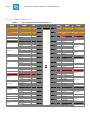
1
TQMa35
User's Manual
TQMa35 UM 103
28.03.2013
User's Manual l TQMa35 UM 103 l © 2013 by TQ-Group
Page i
Table of contents
1.
1.1
1.2
1.3
1.4
1.5
1.6
1.7
1.8
1.9
1.10
2.
3.
3.1
3.1.1
3.1.2
3.1.2.1
3.1.2.2
3.1.2.3
4.
4.1
4.1.1
4.1.2
4.1.2.1
4.1.2.2
4.1.2.3
4.1.3
4.1.3.1
4.1.3.2
4.1.3.3
4.1.4
4.2
4.3
4.3.1
4.3.1.1
4.3.1.2
4.3.1.3
4.3.1.4
ABOUT THIS MANUAL ...................................................................................................................... 1
Copyright ............................................................................................................................................. 1
Tips on safety ...................................................................................................................................... 1
Symbols and Typographic Conventions .................................................................................... 1
Handling and ESD tips ..................................................................................................................... 2
Registered trademarks..................................................................................................................... 2
Imprint .................................................................................................................................................. 3
Disclaimer ............................................................................................................................................ 3
Copyright and licence expenses................................................................................................... 3
Further applicable documents / presumed knowledge ....................................................... 4
Acronyms and definitions............................................................................................................... 5
BRIEF DESCRIPTION .......................................................................................................................... 7
TECHNICAL DATA .............................................................................................................................. 8
System architecture and functionality........................................................................................ 8
TQMa35 block diagram ................................................................................................................... 8
System functionality......................................................................................................................... 9
System components......................................................................................................................... 9
Interfaces ............................................................................................................................................. 9
Diagnosis LED ..................................................................................................................................... 9
ELECTRONICS SPECIFICATION ..................................................................................................... 10
Interfaces to other systems and devices .................................................................................. 10
Module connectors ......................................................................................................................... 10
Pin assignment................................................................................................................................. 11
Module connector X1 .................................................................................................................... 12
Module connector X2 .................................................................................................................... 13
Module connector X3 .................................................................................................................... 14
Pin description ................................................................................................................................. 15
Module connector X1 .................................................................................................................... 16
Module connector X2 .................................................................................................................... 20
Module connector X3 ................................................................................................................... 24
Electrical characteristics ................................................................................................................ 27
User's interfaces ............................................................................................................................... 28
System components....................................................................................................................... 28
Processor ............................................................................................................................................ 28
Boot modes ....................................................................................................................................... 31
Memory management ................................................................................................................... 33
Pin multiplexing .............................................................................................................................. 33
CPU-Errata ......................................................................................................................................... 33
Page ii
User's Manual l TQMa35 UM 103 l © 2013 by TQ-Group
Table of contents (continued)
4.3.2
4.3.2.1
4.3.2.2
4.3.2.3
4.3.2.4
4.3.3
4.3.4
4.3.5
4.3.6
4.3.7
4.3.7.1
4.3.7.2
4.3.8
4.3.8.1
4.3.8.2
4.3.9
4.3.10
4.3.10.1
4.3.10.2
4.3.10.3
4.3.10.4
4.3.10.5
4.3.10.6
4.3.10.7
4.3.10.8
4.3.10.9
4.3.11
4.3.12
4.3.13
4.3.14
4.3.15
4.3.16
4.3.17
4.3.18
Memory .............................................................................................................................................. 34
mDDR SDRAM .................................................................................................................................. 34
NOR flash............................................................................................................................................ 34
eMMC .................................................................................................................................................. 35
EEPROM .............................................................................................................................................. 36
WEIM bus .......................................................................................................................................... 36
RTC ....................................................................................................................................................... 37
Temperature sensor ....................................................................................................................... 37
SD card................................................................................................................................................ 37
Graphics interfaces ......................................................................................................................... 38
LCD bus .............................................................................................................................................. 38
Sensor interface ............................................................................................................................... 38
USB Hi-Speed .................................................................................................................................... 39
USB On-The-Go ................................................................................................................................ 39
USB Host............................................................................................................................................. 40
Ethernet .............................................................................................................................................. 41
Serial interfaces ................................................................................................................................ 42
UART1 / RS232 .................................................................................................................................. 42
UART2 ................................................................................................................................................. 43
UART3 ................................................................................................................................................. 43
I2C bus ................................................................................................................................................. 44
CAN ...................................................................................................................................................... 45
SPI1 ...................................................................................................................................................... 45
SPI2 ...................................................................................................................................................... 45
SSI ......................................................................................................................................................... 45
1-Wire .................................................................................................................................................. 46
PWM .................................................................................................................................................... 46
Keypad ................................................................................................................................................ 46
GPIO ..................................................................................................................................................... 46
Timer ................................................................................................................................................... 46
BDM/JTAG.......................................................................................................................................... 47
Power management ....................................................................................................................... 47
Voltage supervision ........................................................................................................................ 48
Backup supply .................................................................................................................................. 48
User's Manual l TQMa35 UM 103 l © 2013 by TQ-Group
Page iii
Table of contents (continued)
5.
6.
6.1
6.2
6.3
6.4
6.5
6.5.1
6.5.2
6.5.3
7.
7.1
7.2
7.3
7.4
7.5
7.6
7.6.1
7.6.2
7.6.3
8.
8.1
SOFTWARE SPECIFICATION .......................................................................................................... 49
MECHANICS SPECIFICATION ........................................................................................................ 49
General information ....................................................................................................................... 49
Dimensions and stacks heights................................................................................................... 49
Notes of treatment.......................................................................................................................... 50
Component placement ................................................................................................................. 51
Requirements for the higher-level system .............................................................................. 52
Protection against external effects ............................................................................................ 52
Thermal management ................................................................................................................... 52
Structural requirements ................................................................................................................ 52
SAFETY REQUIREMENTS AND PROTECTIVE REGULATIONS ................................................ 53
EMC requirements .......................................................................................................................... 53
ESD requirements............................................................................................................................ 53
Operational safety and personal security ................................................................................ 53
Climatic and operational conditions ......................................................................................... 53
Reliability and service life.............................................................................................................. 54
Environment protection................................................................................................................ 54
RoHS compliance ............................................................................................................................ 54
WEEE regulation .............................................................................................................................. 54
Other entries ..................................................................................................................................... 54
APPENDIX .......................................................................................................................................... 55
References ......................................................................................................................................... 55
Page iv
User's Manual l TQMa35 UM 103 l © 2013 by TQ-Group
Table directory
Table 1:
Table 2:
Table 3:
Table 4:
Table 5:
Table 6:
Table 7:
Table 8:
Table 9:
Table 10:
Table 11:
Table 12:
Table 13:
Table 14:
Table 15:
Table 16:
Table 17:
Table 18:
Table 19:
Table 20:
Table 21:
Table 22:
Table 23:
Table 24:
Table 25:
Table 26:
Table 27:
Table 28:
Table 29:
Terms and conventions ............................................................................................................. 1
Acronyms ....................................................................................................................................... 5
Module connectors used on the TQMa35 ......................................................................... 10
Suitable carrier board mating connectors......................................................................... 11
Pin assignment module connector X1 ............................................................................... 12
Pin assignment module connector X2 ............................................................................... 13
Pin assignment module connector X3 ............................................................................... 14
Pin description X1 ..................................................................................................................... 16
Pin description X2 ..................................................................................................................... 20
Pin description X3 ..................................................................................................................... 24
Electrical characteristics of digital I/Os ............................................................................... 27
Electrical characteristics of the physical signals .............................................................. 28
State of the Reset-LED ............................................................................................................. 28
Processor derivatives ............................................................................................................... 29
Configurable boot pins on the TQMa35 ............................................................................ 31
Possible boot mode configurations for the TQMa35 ..................................................... 32
External Memory allocation ................................................................................................... 33
Memory models mDDR SDRAM............................................................................................ 34
Memory model NOR flash....................................................................................................... 34
Memory model eMMC flash ................................................................................................... 35
Memory model EEPROM ......................................................................................................... 36
Parameter 32.768 kHz crystal oscillator.............................................................................. 37
Transfer modes SD interfaces ................................................................................................ 37
I2C device configuration .......................................................................................................... 44
Technical parameters module supply................................................................................. 47
Trigger levels TPS3801-01 ...................................................................................................... 48
Technical parameters backup input .................................................................................... 48
Height dimensions.................................................................................................................... 50
Further applicable documents.............................................................................................. 55
User's Manual l TQMa35 UM 103 l © 2013 by TQ-Group
Page v
Illustration directory
Illustration 1:
Illustration 2:
Illustration 3:
Illustration 4:
Illustration 5:
Illustration 6:
Illustration 7:
Illustration 8:
Illustration 9:
Illustration 10:
Illustration 11:
Illustration 12:
Illustration 13:
Illustration 14:
Illustration 15:
Illustration 16:
Illustration 17:
Illustration 18:
Illustration 19:
Illustration 20:
TQMa35 block diagram .................................................................................................. 8
i.MX35 block diagram ................................................................................................... 29
Interface WEIM bus ........................................................................................................ 36
Interface LCD ................................................................................................................... 38
Interface CSI ..................................................................................................................... 38
Interface USB OTG .......................................................................................................... 39
USB Hi-Speed OTG workaround ................................................................................ 39
Interface USB host.......................................................................................................... 40
Interface Ethernet MII ................................................................................................... 41
Interface UART1 / RS232 .............................................................................................. 42
Interface UART2 .............................................................................................................. 43
Interface UART3 .............................................................................................................. 43
Interface I2C buses.......................................................................................................... 44
Interface SSI ..................................................................................................................... 45
Timing diagram of a GPIO wakeup interrupt ........................................................ 46
Interface BDM/JTAG ...................................................................................................... 47
Overall dimensions (top view through board)...................................................... 49
Stacks heights (not to scale) ....................................................................................... 49
Component placement top ........................................................................................ 51
Component placement bottom ................................................................................ 51
User's Manual l TQMa35 UM 103 l © 2013 by TQ-Group
Page vi
Revision history
Rev. Date
Name
100
Petz
30.03.2011
Pos.
Document created
2
All
4.3.10.2
4.3.10.3
Petz
Modification
Power consumption corrected
USB signal names corrected
Syntax of signals RTS# and CTS# corrected
Syntax of signals RTS# and CTS# corrected
Information about gold-plating corrected
Values for current consumption updated
Values for current consumption updated
Values for current consumption “Idle” and “Standby” added
Reference (11) added
101
06.12.2011
102
24.05.2012
Petz
Section 5
Link to Wiki added
103
28.03.2013
Petz
All
Typo
Table 4
4.3.16
Table 25
Table 25
Table 29
User's Manual l TQMa35 UM 103 l © 2013 by TQ-Group
1.
ABOUT THIS MANUAL
1.1
Copyright
Page 1
Copyright protected © 2013 by TQ-Systems GmbH.
This User’s Manual may not be copied, reproduced, translated, changed or distributed,
completely or partially in electronic, machine readable, or in any other form without the written
consent of TQ-Systems GmbH.
1.2
Tips on safety
Improper or incorrect handling of the product can substantially reduce its life span.
1.3
Symbols and Typographic Conventions
Table 1:
Terms and conventions
Symbol / Visual Cue
Meaning
This symbol represents the handling of electrostatic-sensitive
modules and / or components. These components are often
damaged / destroyed by the transmission of a voltage higher than
about 50 V. A human body usually only experiences electrostatic
discharges above approximately 3,000 V.
This symbol indicates the possible use of voltages higher than 24 V.
Please note the relevant statutory regulations in this regard. Noncompliance with these regulations can lead to serious damage to
your health and cause damage / destruction of the component.
This symbol indicates a possible source of danger. Acting against the
procedure described can lead to possible damage to your health
and / or cause damage / destruction of the material used.
This symbol represents important details or aspects for working with
TQ-products.
Command
This specification is used to state the complete file name with its
corresponding extension.
User's Manual l TQMa35 UM 103 l © 2013 by TQ-Group
Page 2
1.4
Handling and ESD tips
General handling of your TQ-products
The TQ-product may only be used and serviced by certified
personnel who have taken note of the information, the safety
regulations in this document and all related rules and regulations.
A general rule is: do not touch the TQ-product during operation. This
is especially important when switching on, changing jumper settings
or connecting other devices without ensuring beforehand that the
power supply of the system has been switched off.
Violation of this guideline may result in damage / destruction of the
module and be dangerous to your health.
Improper handling of your TQ-product would render the guarantee
invalid.
Proper ESD handling
The electronic components of your TQ-product are sensitive to
electrostatic discharge (ESD).
Always wear antistatic clothing, use ESD-safe tools, packing materials
etc., and operate your TQ-product in an ESD-safe environment.
Especially when you switch modules on, change jumper settings, or
connect other devices.
1.5
Registered trademarks
TQ-Systems GmbH aims to adhere to the copyrights of all the used graphics and texts in all
publications and strives to use original or license-free graphics and texts.
All the brand names and trademarks mentioned in the publication, including those protected by
a third party, unless specified otherwise in writing, are subjected to the specifications of the
current copyright laws and the proprietary laws of the present registered proprietor without any
limitation. One should conclude that brands and trademarks are protected through the rights of
a third party.
User's Manual l TQMa35 UM 103 l © 2013 by TQ-Group
1.6
Page 3
Imprint
TQ-Systems GmbH
Gut Delling, Mühlstraße 2
82229 Seefeld
Tel:
+49 (0) 8153 9308–0
Fax:
+49 (0) 8153 9308–134
Email: [email protected]
Web:
http://www.tq-group.com/
1.7
Disclaimer
TQ-Systems GmbH does not guarantee that the information in this manual is up-to-date, correct,
complete or of good quality. Nor does TQ-Systems assume guarantee for further usage of the
information. Liability claims against TQ-Systems GmbH, referring to material or non-material
related damages, caused due to usage or non-usage of the information given in the manual, or
caused due to usage of erroneous or incomplete information, are exempted, as long as there is
no proven, intentional or negligent fault of TQ-Systems GmbH.
TQ-Systems GmbH explicitly reserves the rights to change or add to the contents of this manual
or parts of it without special notification.
1.8
Copyright and licence expenses
e xpenses
The drivers and utilities for the used components as well as the BIOS are subject to the
copyrights of the respective manufacturers. The licence conditions of the respective
manufacturer are to be adhered to.
Bootloader-licence expenses are paid by TQ and are included in the price.
Licence expenses for the operating system and applications are not taken into consideration and
must be separately calculated / declared.
Page 4
1.9
User's Manual l TQMa35 UM 103 l © 2013 by TQ-Group
Further applicable documents / presumed knowledge
•
Specifications and manual of the
th e used modules:
These documents describe the service, functionality and special characteristics of the
used module (incl. BIOS).
•
Specifications of the used components:
The manufacturer's specifications of the used components, for example Compact-Flash
cards, are to be taken note of. They contain, if applicable, additional information that
must be taken note of for safe and reliable operation. These documents are stored at TQ.
•
Chip errata:
It is the user's responsibility to make sure all errata published by the manufacturer of
each component are taken note of. The manufacturer’s advice should be followed.
•
Software behaviour:
No warranty can be given, nor responsibility taken for any unexpected software
behaviour due to deficient components.
•
General expertise:
expertise:
Expertise in electrical engineering / computer engineering is required for the installation
and the use of the device.
User's Manual l TQMa35 UM 103 l © 2013 by TQ-Group
1.10
Acronyms and definitions
The following acronyms and abbreviations are used in this document:
Table 2:
Acronyms
Acronym
Meaning
ARM®
ATA
BDM
BGA
BSP
CAN
CCD
CE-ATA
CMOS
CPU
DDR
DNC
ECC
EEPROM
EMC
eMMC
ESD
FEC
FR-4
GPIO
GPU
I/O
IP00
IPU
I2C
JTAG
LCD
LED
LSB
LVTTL
Mbps
mDDR
MIC
MII
Advanced RISC Machine
Advanced Technology Attachment
Background Debug Mode
Ball Grid Array
Board Support Package
Controller Area Network
Charge-Coupled Device
Consumer Electronics-Advanced Technology Attachment
Complementary Metal Oxide Semiconductor
Central Processing Unit
Double Data Rate
Do Not Connect
Error Checking and Correction
Electrically Erasable Programmable Read-only Memory
Electromagnetic Compatibility
embedded MultiMediaCard (Flash)
Electrostatic Discharge
Fast Ethernet Controller
Flame Retardant-4
General Purpose Input/Output
Graphics Processor Unit
Input/Output
Ingress Protection 00
Image Processing Unit
Inter-Integrated Circuit
Joint Test Action Group
Liquid Crystal Display
Light Emitting Diode
Least Significant Bit
Low Voltage Transistor Transistor Logic
Megabit per second
mobile Double Data Rate
Microphone
Media-Independent Interface
Page 5
User's Manual l TQMa35 UM 103 l © 2013 by TQ-Group
Page 6
Table 2:
Acronyms (continued)
Acronym
Meaning
MMC
MMCA
MOZI
MSB
MTBF
NAND
NC
NOR
OTG
PATA
PCB
PHY
Ppm
PSRAM
PWM
RAM
RF
RoHS
ROM
RTC
SD
SDIO
SDRAM
SMD
SPI
SRAM
SSI
UART
UL
ULPI
USB
USB-HS
UTMI
WEEE
WEIM
WP
WVGA
Multimedia Card
MultiMediaCard Association
Module extractor (Modulzieher)
Most Significant Bit
Mean operating Time Between Failures
Not-and
Not Connected
Not-or
On-The-Go
Parallel ATA
Printed Circuit Board
Physical (Interface)
Parts Per Million
CellularRAM ™
Pulse Width Modulation
Random Access Memory
Radio Frequency
Restriction of (the use of certain) Hazardous Substances
Read-Only Memory
Real-Time Clock
Secure Digital
Secure Digital Input/Output
Synchronous Dynamic Random Access Memory
Surface-Mounted Device
Serial Peripheral Interface
Static Random Access Memory
Synchronous Serial Interface
Universal Asynchronous Receiver/Transmitter
Underwriters Laboratories Inc.
UTMI+ Low Pin Interface
Universal Serial Bus
Universal Serial Bus - High Speed
USB 2.0 Transceiver Macrocell Interface
Waste Electrical and Electronic Equipment
Wireless External Interface Module
Write-Protection
Wide Video Graphics Array (800 × 480)
User's Manual l TQMa35 UM 103 l © 2013 by TQ-Group
2.
Page 7
BRIEF DESCRIPTION
The TQMa35 is a universal Minimodule with a Freescale ARM-CPU MCIMX35 (i.MX35).
The ARM1136 core works with up to 532 MHz. The module extends the TQC product range and
offers a well-balanced ratio between computing performance and graphics power.
The module offers the following key functions and characteristics:
•
•
•
•
•
•
•
•
•
•
•
•
•
•
•
•
•
Freescale i.MX353 (ARM11 architecture), 532 MHz
Integrated hardware acceleration for IPU and GPU
All functional CPU pins are routed to module connectors
Up to 128 MiB NOR Flash
Up to 512 MiB mDDR-SDRAM
eMMC flash (option)
1 × USB 2.0 Hi-Speed Host interface
1 × USB 2.0 Hi-Speed OTG
Temperature sensor
RTC
EEPROM
RS232-Transceiver on-board
Single power supply: 3.3 V
Low power consumption (typical 1 – 1.5 W)
Dimensions: 54 × 44 mm2
Easy and cost-efficient carrier board development
Long term available
Since almost all functional pins of the processor (except SDRAM interface) are routed to the
module connectors, there is a wide range of possible applications for the TQMa35.
User's Manual l TQMa35 UM 103 l © 2013 by TQ-Group
Page 8
3.
TECHNICAL DATA
3.1
System architecture and functionality
3.1.1
TQMa35 block diagram
120-pin plug connector
80-pin plug connector
Tyco 5353999-5
Tyco 5177985-3
USB-ULPI-PHY
3 x driver
ISP1504C1
74 AVCH 16T 245ZQLR
NOR-Flash
(max. 128 MiB)
PC28F256M29EWL
USB OTG / CONFIG / SD1 / LCD / Sensor - IPU /
SSI 4 / JTAG / PWM
WEIM
ESDRAMC
USBH2
I2C2
CPU
i.MX35
(2x) mDDR-RAM
(max. 512 MiB)
H5MS 2G22 MFR-J3M
EEPROM
(max . 64 Kibit)
M24C64-WDW6TP
RTC
DS1339U-33+
UART1
ETH MII / SPI 1+2 / CAN 1+2 / I2C 1 / UART 2+3 / 4 x4
Keypad / 1-Wire / Timer / GPIOs
SD3
Temp.-sensor
RS232- driver
MAX3222
0 R n.a.
LM75CIMM-3
eMMC Flash
(max . 4 GiB)
THGBM1G4D1EBAI7
120-pin plug connector
Tyco 5353999-5
Illustration 1:
TQMa35 block diagram
User's Manual l TQMa35 UM 103 l © 2013 by TQ-Group
3.1.2
System functionality
3.1.2.1
System components
•
•
•
•
•
•
•
•
•
•
•
•
•
3.1.2.2
•
•
Processor (Freescale MCIMX35, ARM1136JF-S, 532 MHz, IPU and GPU)
Crystal oscillators for the CPU (24 MHz and 24.576 MHz)
mDDR-SDRAM (32 Bit, 133 MHz, up to 2 devices parallel with 256 MiB each) 1
NOR flash (16 Bit, up to 128 MiB) 2
eMMC NAND flash (up to 4 GiB, SD3 interface at X1 not usable) 3
EEPROM (via I2C, up to 64 Kibit) 3
Temperature sensor (via I2C)
Separate RTC (via I2C, battery buffering possible)
Crystal oscillator for RTC (32.768 kHz)
RS232 driver (at UART1, RxD and TxD)
USB-ULPI-PHY (Hi-Speed)
Level converter (3.3 V VCCI/O for all signals at the module connectors)
Power Management (Power-Up sequencing, voltage supervision,
Boot mode configuration, Reset)
Interfaces
2 × 120-pin module connector
1 × 80-pin module connector 3
A detailed overview of all available user interfaces can be found in section 4.1 on page 10.
3.1.2.3
•
1
2
3
Diagnosis LED
Indication of reset condition
Size of mDDR-SDRAM depends on placement option.
Size of NOR-Flash depends on placement option.
Depends on placement option.
Page 9
User's Manual l TQMa35 UM 103 l © 2013 by TQ-Group
Page 10
4.
ELECTRONICS SPECIFICATION
SPECIFICATION
4.1
Interfaces to other systems and devices
The TQMa35 is connected to the carrier board with 240 pins on two module connectors,
optionally with 320 pins on three connectors.
The module is held in the connectors with a considerable retention force.
To avoid damaging the modules’ connectors as well as the carrier board connectors while
removing the module the use of an extraction tool is strongly recommended. (For more
information, see section 6.3 on page 50).
4.1.1
Module connectors
Table 3:
Module connectors used on the TQMa35
Manufacturer / Part No.
Description
tyco / 5353999-5
−
−
−
−
120-pin connector
0.8 mm pitch
vertical
–40 °C to +85 °C
tyco 4 / 5177985-3
−
−
−
−
80- pin connector
0.8 mm pitch
vertical
–40 °C to +85 °C
The following table shows suitable mating connectors for the carrier board.
4
Depends on placement option.
User's Manual l TQMa35 UM 103 l © 2013 by TQ-Group
Table 4:
Manufacturer
Page 11
Suitable carrier board mating connectors
Part No.
No. of pins
Plating
Board to board distance
(see Illustration 18)
tyco
5177986-5
120
0.2 µm Gold
5 mm
tyco
5-5177986-5
120
0.76 µm Gold
5 mm
tyco
1-5177986-5
120
0.2 µm Gold
6 mm
tyco
6-5177986-5
120
0.76 µm Gold
6 mm
tyco
2-5177986-5
120
0.2 µm Gold
7 mm
tyco
--------------
120
0.76 µm Gold
7 mm
tyco
3-5177986-5
120
0.2 µm Gold
8 mm
tyco
6123001-5
120
0.76 µm Gold
8 mm
tyco
5177986-3
80
0.2 µm Gold
5 mm
tyco
5-5177986-3
80
0.76 µm Gold
5 mm
tyco
1-5177986-3
80
0.2 µm Gold
6 mm
tyco
6-5177986-3
80
0.76 µm Gold
6 mm
tyco
2-5177986-3
80
0.2 µm Gold
7 mm
tyco
--------------
80
0.76 µm Gold
7 mm
tyco
3-5177986-3
80
0.2 µm Gold
8 mm
tyco
6123001-3
80
0.76 µm Gold
8 mm
4.1.2
Pin assignment
When using the processor signals the multiple pin configurations by different processor-internal
function units must be taken note of.
The pins assignment listed in sections 4.1.2.1 to 4.1.2.3 refer to the corresponding standard BSP
of TQ-Systems GmbH.
User's Manual l TQMa35 UM 103 l © 2013 by TQ-Group
Page 12
Module connector X1
Table 5:
Group
Power
Power
Power
Power
Power
Power
General clock
Power
GPIO
Power
GPIO
Power
4x4 keypad
Power
1-Wire
SPI 1
Power
SPI 1
Power
Timer
SD card 3
Power
SD card 3
Power
Ethernet MII
Power
Ethernet MII
Power
CAN 2
CAN 1
UART 3
Power
UART 2
Power
Pin assignment module connector X1
Signal
VCC3V3
VCC3V3
VCC3V3
VCC3V3
VBAT
DGND
CLKO
DGND
GPIO1_4
GPIO1_5
DGND
GPIO2_7
GPIO2_18
GPIO2_23
GPIO2_25
DGND
ROW0
ROW1
ROW2
ROW3
DGND
OWDAT
SPI1_SS0
SPI1_SS1
SPI1_SS3
DGND
SPI1_CLK
SPI1_MISO
SPI1_MOSI
SPI1_RDY
DGND
TIM_CAPIN1
TIM_CMPOUT1
SD3_CMD
SD3_CLK
DGND
SD3_DAT4
SD3_DAT5
SD3_DAT6
SD3_DAT7
DGND
FEC_TXD3
FEC_TX_ER
FEC_TX_EN
FEC_RXD1
DGND
FEC_RXD3
FEC_RX_ER
FEC_RX_DV
FEC_MDC
DGND
CAN2_TX
CAN1_TX
CAN1_RX
UART3_CTS#
DGND
UART2_RTS#
UART2_TXD
UART2_RXD
DGND
I/O
P
P
P
P
P
P
O
P
I/O
I/O
P
I/O
I/O
I/O
I/O
P
I/O
I/O
I/O
I/O
P
I/O
I/O
I/O
I/O
P
I/O
I/O
I/O
I
P
I
O
I/O
O
P
I/O
I/O
I/O
I/O
P
O
O
O
I
P
I
I
I
O
P
O
O
I
O
P
I
O
I
P
I/O
1
3
5
7
9
11
13
15
17
19
21
23
25
27
29
31
33
35
37
39
41
43
45
47
49
51
53
55
57
59
61
63
65
67
69
71
73
75
77
79
81
83
85
87
89
91
93
95
97
99
101
103
105
107
109
111
113
115
117
119
X1
4.1.2.1
2
4
6
8
10
12
14
16
18
20
22
24
26
28
30
32
34
36
38
40
42
44
46
48
50
52
54
56
58
60
62
64
66
68
70
72
74
76
78
80
82
84
86
88
90
92
94
96
98
100
102
104
106
108
110
112
114
116
118
120
P
P
P
P
P
P
P
P
P
I/O
I/O
I/O
P
I/O
I/O
I/O
I/O
P
I/O
I/O
I/O
I/O
P
I/O
I/O
I/O
I
P
I/O
I/O
I/O
I/O
P
I/O
I/O
I/O
I/O
P
O
O
O
I
P
I
I
P
I
P
I/O
I
I
I
P
I
O
I
O
P
O
I
Signal
VCC3V3
VCC3V3
VCC3V3
VCC3V3
DGND
DGND
DGND
DGND
DGND
GPIO1_12
GPIO1_22
GPIO2_0
DGND
COL0
COL1
COL2
COL3
DGND
GPIO3_3
GPIO3_4
GPIO3_5
SPI2_SS0
DGND
SPI2_CLK
SPI2_MISO
SPI2_MOSI
SPI2_RDY
DGND
I2C1_SCL
I2C1_SDA
I2C2_SCL
I2C2_SDA
DGND
SD3_DAT0
SD3_DAT1
SD3_DAT2
SD3_DAT3
DGND
FEC_TXD0
FEC_TXD1
FEC_TXD2
FEC_TX_CLK
DGND
FEC_RXD0
FEC_RXD2
DGND
FEC_RX_CLK
DGND
FEC_MDIO
FEC_CRS
FEC_COL
CAN2_RX
DGND
UART3_RTS#
UART3_TXD
UART3_RXD
UART2_CTS#
DGND
RS232_TXD
RS232_RXD
Group
Power
Power
Power
Power
Power
Power
Power
Power
Power
GPIO
Power
4x4 keypad
Power
GPIO
SPI 2
Power
SPI 2
Power
I2C 1
I2C 2
Power
SD card 3
Power
Ethernet MII
Power
Ethernet MII
Power
Ethernet MII
Power
Ethernet MII
CAN 2
Power
UART 3
UART 2
Power
RS232
User's Manual l TQMa35 UM 103 l © 2013 by TQ-Group
Module connector X2
Table 6:
Group
Power
Reserve
Power Management
Timer
Power
SSI 4
Power
IPU-LCD
Power
IPU-LCD
Power
IPU-LCD
Power
IPU-LCD
Power
IPU-LCD
Power
USB Host Hi-Speed
Power
USB Host Hi-Speed
Power
USB OTG Hi-Speed
Power
SD card 1
Power
SD card 1
IPU-CSI
Power
IPU-CSI
Power
IPU-CSI
Power
CPU-JTAG
Power
Pin assignment module connector X2
Signal
DGND
NC
NC
VSTBY
PWM
DGND
SSI_TXD
SSI_RXD
SSI_TXC
SSI_TXFS
DGND
LD3
LD5
LD7
LD9
DGND
LD11
LD13
LD15
LD17
DGND
LD19
LD21
LD23
LD_DRDY
DGND
LD_HSYNC
LD_VSYNC
DGND
LD_CLK
DGND
USBHS_UID
DGND
USBHS_UDP
USBHS_UDM
DGND
USB_OTG_DM
USB_OTG_DP
DGND
SD1_CLK
DGND
SD1_CMD
CSI_D1
CSI_D3
CSI_D5
DGND
CSI_D7
CSI_D9
CSI_D11
CSI_D13
DGND
CSI_D15
CSI_VSYNC
CSI_HSYNC
CSI_PIXCLK
DGND
TCK
TMS
TDI
DGND
I/O
P
I
O
P
I/O
I/O
I/O
I/O
P
O
O
O
O
P
O
O
O
O
P
O
O
O
O
P
O
O
P
O
P
I
P
I/O
I/O
P
I/O
I/O
P
O
P
I/O
I
I
I
P
I
I
I
I
P
I
I
I
I
P
I
I
I
P
I/O
1
3
5
7
9
11
13
15
17
19
21
23
25
27
29
31
33
35
37
39
41
43
45
47
49
51
53
55
57
59
61
63
65
67
69
71
73
75
77
79
81
83
85
87
89
91
93
95
97
99
101
103
105
107
109
111
113
115
117
119
X2
4.1.2.2
Page 13
2
4
6
8
10
12
14
16
18
20
22
24
26
28
30
32
34
36
38
40
42
44
46
48
50
52
54
56
58
60
62
64
66
68
70
72
74
76
78
80
82
84
86
88
90
92
94
96
98
100
102
104
106
108
110
112
114
116
118
120
I
I
P
I
I
I
O
P
O
O
O
O
P
O
O
O
O
P
O
O
O
O
P
O
O
O
O
P
O
I
O
I/O
P
I
O
I
I/O
P
I/O
I/O
I/O
I/O
P
I
I
I
I
P
I
I
I
I
P
O
I/O
O
I
P
O
I
Signal
FLASH_RESET#
WP#_ACC
DGND
WDOG_RST#
JTAG_RESET#
RESET_IN#
POR#
DGND
LD0
LD1
LD2
LD4
DGND
LD6
LD8
LD10
LD12
DGND
LD14
LD16
LD18
LD20
DGND
LD22
LD_SPL
LD_REV
LD_CLS
DGND
LD_CONTRAST
USBHS_OC
USBHS_PSW#
USBHS_VBUS
DGND
USB_OTG_OC
USB_OTG_PWR
USB_OTG_UID
USB_OTG_VBUS
DGND
SD1_DAT0
SD1_DAT1
SD1_DAT2
SD1_DAT3
DGND
CSI_D0
CSI_D2
CSI_D4
CSI_D6
DGND
CSI_D8
CSI_D10
CSI_D12
CSI_D14
DGND
CSI_MCLK
DE#
RTCK
JTAG_MOD
DGND
TDO
TRST#
Group
NOR-Flash-CTRL
Power
Reset
Power
IPU-LCD
Power
IPU-LCD
Power
IPU-LCD
Power
IPU-LCD
Power
IPU-LCD
USB Host Hi-Speed
Power
USB OTG Hi-Speed
Power
SD card 1
Power
IPU-CSI
Power
IPU-CSI
Power
IPU-CSI
CPU-JTAG
Power
CPU-JTAG
User's Manual l TQMa35 UM 103 l © 2013 by TQ-Group
Page 14
Module connector X3
Table 7:
Group
Power
16 bit data bus
Power
16 bit data bus
Power
26 bit address bus
Power
26 bit address bus
Power
26 bit address bus
Power
26 bit address bus
Bus-CTRL
Power
Bus-CTRL
Power
Bus-CTRL
Factory test only
Power
Factory test only
Power
Pin assignment module connector X3
Signal
DGND
D1
D3
D5
D7
DGND
D9
D11
D13
D15
DGND
A1
A3
A5
A7
DGND
A9
A11
A13
A15
DGND
A17
A19
A21
A23
DGND
A25
DTACK#
DGND
BUS_CLK
DGND
EB1#
CS1#
CS5#
DNC
DGND
DNC
DNC
DNC
DGND
I/O
P
I/O
I/O
I/O
I/O
P
I/O
I/O
I/O
I/O
P
O
O
O
O
P
O
O
O
O
P
O
O
O
O
P
O
I
P
O
P
O
O
O
P
P
I/O
1
3
5
7
9
11
13
15
17
19
21
23
25
27
29
31
33
35
37
39
41
43
45
47
49
51
53
55
57
59
61
63
65
67
69
71
73
75
77
79
X3
4.1.2.3
2
4
6
8
10
12
14
16
18
20
22
24
26
28
30
32
34
36
38
40
42
44
46
48
50
52
54
56
58
60
62
64
66
68
70
72
74
76
78
80
I/O
I/O
P
I/O
I/O
I/O
I/O
P
I/O
I/O
O
O
P
O
O
O
O
P
O
O
O
O
P
O
O
O
O
P
O
O
I
O
P
P
-
Signal
D0
D2
DGND
D4
D6
D8
D10
DGND
D12
D14
A0
A2
DGND
A4
A6
A8
A10
DGND
A12
A14
A16
A18
DGND
A20
A22
A24
LBA#
DGND
RW#
OE#
ECB#
EB0#
DGND
DNC
DNC
DNC
DNC
DGND
NC
NC
Group
16 bit data bus
Power
16 bit data bus
Power
16 bit data bus
26 bit address bus
Power
26 bit address bus
Power
26 bit address bus
Power
26 bit address bus
Bus-CTRL
Power
Bus-CTRL
Power
Factory test only
Power
Reserve
User's Manual l TQMa35 UM 103 l © 2013 by TQ-Group
4.1.3
Page 15
Pin description
The pins of the module connectors are described in detail in the following tables.
External and internal pull-up or-down wirings as well as the references to I/O voltage and
processor pin characteristics are listed in addition to direction, pin name and pin number.
The processor pin in parentheses () means there is no direct connection between processor and
connector (e.g. via level converter) or that connector and processor are connected to the output
simultaneously.
Attention: Pin characteristics
The entries in Table 8 to Table 10 for direction, internal pull/keeper, slew rate
and drive strength are values for the standard-BSP of TQ-Systems GmbH and can
also be configured differently.
User's Manual l TQMa35 UM 103 l © 2013 by TQ-Group
Page 16
4.1.3.1
Module connector X1
Table 8:
Pin description X1
P
P
P
P
P
P
P
P
–
–
–
–
–
–
–
–
–
–
–
–
–
–
–
–
–
–
–
–
–
–
–
–
9
VBAT
P
–
–
–
10
11
12
13
14
15
16
17
18
19
20
21
DGND
DGND
DGND
CLKO
DGND
DGND
DGND
GPIO1_4
DGND
GPIO1_5
GPIO1_12
DGND
P
P
P
O
P
P
P
I/O
P
I/O
I/O
P
–
–
–
Vi.MX35
–
–
–
Vi.MX35
–
Vi.MX35
Vi.MX35
–
–
–
–
V10
–
–
–
K3
–
K5
J2
–
–
–
–
–
–
–
–
100 kΩ
–
100 kΩ
100 kΩ
–
22 GPIO1_22
I/O
Vi.MX35
G3
23
24
25
26
27
28
29
30
31
I/O
I/O
I/O
P
I/O
I/O
I/O
I/O
P
Vi.MX35
Vi.MX35
Vi.MX35
–
Vi.MX35
Vi.MX35
Vi.MX35
Vi.MX35
–
T7
U11
W4
–
F3
H5
U3
H1
–
GPIO2_7
GPIO2_0
GPIO2_18
DGND
GPIO2_23
COL0
GPIO2_25
COL1
DGND
Remark
Drive
strength
Internal pull
/ Keeper
VIN
VIN
VIN
VIN
VIN
VIN
VIN
VIN
Slew rate
CPU-Pin
1
2
3
4
5
6
7
8
Pin Pin name
Direction
VCCIO
External pullup / -down
i.MX35 Parameter
See section 4.3.18
on page 48
Fast
Max
Slow
Nom
Slow
Slow
Nom
Nom
–
Fast
Nom
–
Keeper
100 kΩ
–
100 kΩ
100 kΩ
100 kΩ
100 kΩ
–
Slow
Slow
Slow
Nom
Nom
Nom
Fast
Slow
Slow
Slow
Nom
Nom
Nom
Nom
Optional interrupt signal of RTC
Optional overtemperature
signal of temperature sensor
User's Manual l TQMa35 UM 103 l © 2013 by TQ-Group
Table 8:
Pin description X1 (continued)
I/O
I/O
I/O
I/O
P
I/O
I/O
I/O
I/O
P
I/O
I/O
I/O
I/O
P
I/O
I/O
I/O
I/O
P
I/O
I/O
I
I/O
P
I/O
I/OOD
I
I/OOD
P
I/OOD
I
I/OOD
O
1.2 kΩ
1.2 kΩ
–
1.2 kΩ
1.2 kΩ
–
Remark
Drive
strength
G4
W1
J5
T4
–
J4
W13
J1
Y13
–
W12
T11
K2
Y8
–
U8
L5
V7
K4
–
K1
W8
J6
V9
–
W9
M20
T8
N17
–
L3
V12
M1
T12
Slew rate
Vi.MX35
Vi.MX35
Vi.MX35
Vi.MX35
–
Vi.MX35
Vi.MX35
Vi.MX35
Vi.MX35
–
Vi.MX35
Vi.MX35
Vi.MX35
Vi.MX35
–
Vi.MX35
Vi.MX35
Vi.MX35
Vi.MX35
–
Vi.MX35
Vi.MX35
Vi.MX35
Vi.MX35
–
Vi.MX35
Vi.MX35
Vi.MX35
Vi.MX35
–
Vi.MX35
Vi.MX35
Vi.MX35
Vi.MX35
Internal pull
/ Keeper
CPU-Pin
COL2
ROW0
COL3
ROW1
DGND
ROW2
GPIO3_3
ROW3
GPIO3_4
DGND
GPIO3_5
OWDAT
SPI2_SS0
SPI1_SS0
DGND
SPI1_SS1
SPI2_CLK
SPI1_SS3
SPI2_MISO
DGND
SPI2_MOSI
SPI1_CLK
SPI2_RDY
SPI1_MISO
DGND
SPI1_MOSI
I2C1_SCL
SPI1_RDY
I2C1_SDA
DGND
I2C2_SCL
TIM_CAPIN1
I2C2_SDA
TIM_CMPOUT1
VCCIO
32
33
34
35
36
37
38
39
40
41
42
43
44
45
46
47
48
49
50
51
52
53
54
55
56
57
58
59
60
61
62
63
64
65
External pullup / -down
Pin Pin name
Direction
i.MX35 Parameter
100 kΩ
100 kΩ
100 kΩ
100 kΩ
–
100 kΩ
100 kΩ
100 kΩ
100 kΩ
–
100 kΩ
Keeper
100 kΩ
100 kΩ
–
100 kΩ
100 kΩ
–
100 kΩ
–
100 kΩ
100 kΩ
100 kΩ
100 kΩ
–
100 kΩ
100 kΩ
100 kΩ
100 kΩ
Slow
Slow
Slow
Slow
Nom
Nom
High
Nom
Slow
Fast
Slow
Fast
Nom
Nom
Nom
Nom
Fast
Slow
Slow
Slow
Nom
Nom
High
Nom
Slow
Slow
Slow
Slow
Nom
Nom
Nom
Nom
Slow
Slow
Slow
Slow
Nom
Nom
Nom
Nom
Slow
Slow
Slow
Slow
Nom
Nom
Nom
Nom
100 kΩ
100 kΩ
100 kΩ
100 kΩ
Slow
Slow
Slow
Slow
Nom
Nom
Nom
Nom
Page 17
User's Manual l TQMa35 UM 103 l © 2013 by TQ-Group
Page 18
Table 8:
Pin description X1 (continued)
–
I/O
10 kΩ
Vi.MX35
Y4
68 SD3_DAT0
I/O
10 kΩ 5 Vi.MX35
Y6
69 SD3_CLK
O
Vi.MX35
U5
70 SD3_DAT1
I/O
10 kΩ 5 Vi.MX35
W6
P
–
5
–
–
72 SD3_DAT2
I/O
10 kΩ
Vi.MX35
V6
73 SD3_DAT4
I/O
10 kΩ 5 Vi.MX35
U6
74 SD3_DAT3
I/O
10 kΩ 5 Vi.MX35
T6
75 SD3_DAT5
I/O
10 kΩ 5 Vi.MX35
Y5
76 DGND
P
–
77 SD3_DAT6
I/O
10 kΩ
78 FEC_TXD0
O
–
79 SD3_DAT7
I/O
80
81
82
83
84
85
86
87
88
O
P
O
O
I
O
P
O
I
FEC_TXD1
DGND
FEC_TXD2
FEC_TXD3
FEC_TX_CLK
FEC_TX_ER
DGND
FEC_TX_EN
FEC_RXD0
10 kΩ
5
5
100 kΩ
Slow
Nom
Slow
Nom
Slow
Nom
Slow
Nom
Slow
Nom
Slow
Nom
Slow
Nom
100 kΩ
Slow
Nom
100 kΩ
Slow
Nom
Slow
Nom
100 kΩ
100 kΩ
Remark
Drive
strength
–
5
Slew rate
–
Internal pull
/ Keeper
CPU-Pin
P
67 SD3_CMD
71 DGND
5
VCCIO
66 DGND
External pullup / -down
Pin Pin name
Direction
i.MX35 Parameter
–
–
Vi.MX35
W5
Vi.MX35
P5
Vi.MX35
V5
100 kΩ
Slow
Nom
Vi.MX35
–
Vi.MX35
Vi.MX35
Vi.MX35
Vi.MX35
–
Vi.MX35
Vi.MX35
M4
–
M5
L6
P4
N4
–
T1
P2
–
–
–
–
100 kΩ
–
–
–
100 kΩ
Slow
Nom
Slow
Slow
Slow
Slow
Nom
Nom
Nom
Nom
Slow
Slow
Nom
Nom
Pull-up only assembled when eMMC is assembled.
Do not connect when
eMMC is assembled
Do not connect when
eMMC is assembled
Do not connect when
eMMC is assembled
Do not connect when
eMMC is assembled
Do not connect when
eMMC is assembled
Do not connect when
eMMC is assembled
Do not connect when
eMMC is assembled
Do not connect when
eMMC is assembled
Do not connect when
eMMC is assembled
Do not connect when
eMMC is assembled
User's Manual l TQMa35 UM 103 l © 2013 by TQ-Group
Table 8:
Page 19
Pin description X1 (continued)
6
1.5 kΩ
N2
M3
–
–
N1
R2
N3
–
T2
P1
R1
N5
–
P3
J3
H4
V4
–
Y3
U4
W15
Y2
–
V3
G1
G5
H2
–
H3
(R6)
–
(U2)
100 kΩ
100 kΩ
–
–
100 kΩ
100 kΩ
100 kΩ
–
100 kΩ
22 kΩ
–
100 kΩ
–
100 kΩ
100 kΩ
100 kΩ
100 kΩ
–
100 kΩ
100 kΩ
100 kΩ
100 kΩ
–
100 kΩ
100 kΩ
–
–
–
100 kΩ
–
–
–
Remark
Drive
strength
Vi.MX35
Vi.MX35
–
–
Vi.MX35
Vi.MX35
Vi.MX35
–
Vi.MX35
Vi.MX35
Vi.MX35
Vi.MX35
–
Vi.MX35
Vi.MX35
Vi.MX35
Vi.MX35
–
Vi.MX35
Vi.MX35
Vi.MX35
Vi.MX35
–
Vi.MX35
Vi.MX35
Vi.MX35
Vi.MX35
–
Vi.MX35
VRS232
–
VRS232
Slew rate
Internal pull
/ Keeper
I
I
P
P
I
I
I
P
I
I/O
O
I
P
I
I/O
I
I/O
P
I/O
I
O
O
P
I
I
O
O
P
I
O
P
I
CPU-Pin
FEC_RXD1
FEC_RXD2
DGND
DGND
FEC_RXD3
FEC_RX_CLK
FEC_RX_ER
DGND
FEC_RX_DV
FEC_MDIO
FEC_MDC
FEC_CRS
DGND
FEC_COL
CAN2_TX
CAN2_RX
CAN1_TX
DGND
CAN1_RX
UART3_RTS#
UART3_CTS#
UART3_TXD
DGND
UART3_RXD
UART2_RTS#
UART2_CTS#
UART2_TXD
DGND
UART2_RXD
RS232_TXD 6
DGND
RS232_RXD 6
VCCIO
89
90
91
92
93
94
95
96
97
98
99
100
101
102
103
104
105
106
107
108
109
110
111
112
113
114
115
116
117
118
119
120
External pullup / -down
Pin Pin name
Direction
i.MX35 Parameter
Slow
Slow
Nom
Nom
Slow
Slow
Slow
Nom
Nom
Nom
Slow
Slow
Slow
Slow
Nom
Nom
Nom
Nom
Slow
Slow
Slow
Slow
Nom
Nom
Nom
Nom
Slow
Slow
Slow
Slow
Nom
Nom
Nom
Nom
Slow
Slow
Slow
Slow
Nom
Nom
Nom
Nom
Slow
Nom
VCCIO depends on placement option (if UART1 is used instead of RS232, then VCCIO = Vi.MX35).
Optionally UART1_TxD
Optionally UART1_RxD
User's Manual l TQMa35 UM 103 l © 2013 by TQ-Group
Page 20
4.1.3.2
Module connector X2
Table 9:
Pin description X2
Internal pull
/ Keeper
–
–
–
I
18 kΩ
VNOR
–
3
NC
–
–
–
–
Not connected
4
5
WP#_ACC
NC
I
–
10 kΩ
–
VNOR
–
–
–
Not connected
6
DGND
P
–
–
–
7
VSTBY
I
–
Vi.MX35
T9
Slow
Nom
8
WDOG_RST#
I
10 kΩ
Vi.MX35
Y12
100 kΩ
Slow
Nom
9
PWM
O
–
Vi.MX35
Y11
Keeper
Slow
Nom
10
JTAG_RESET#
I
10 kΩ
VDRV
(U10)
11
DGND
P
–
–
–
12
RESET_IN#
I
10 kΩ
VDRV
(U10)
13
SSI_TXD
I/O
–
Vi.MX35
M2
100 kΩ
Slow
Nom
14
POR#
O
10 kΩ
VPOR
(W11)
15
SSI_RXD
I/O
–
Vi.MX35
L1
100 kΩ
Slow
Nom
16
DGND
P
–
–
–
17
SSI_TXC
I/O
–
Vi.MX35
L4
100 kΩ
Slow
Nom
18
LD0
O
–
Vi.MX35
F20
100 kΩ
Fast
Nom
19
SSI_TXFS
I/O
–
Vi.MX35
L2
100 kΩ
Slow
Nom
20
LD1
O
–
Vi.MX35
G18
100 kΩ
Fast
Nom
21
DGND
P
–
–
–
22
LD2
O
–
Vi.MX35
G17
100 kΩ
Fast
Nom
23
LD3
O
–
Vi.MX35
G16
100 kΩ
Fast
Nom
24
LD4
O
–
Vi.MX35
G19
100 kΩ
Fast
Nom
25
LD5
O
–
Vi.MX35
H16
100 kΩ
Fast
Nom
26
DGND
P
–
–
–
27
LD7
O
–
Vi.MX35
G20
100 kΩ
Fast
Nom
28
LD6
O
–
Vi.MX35
H18
100 kΩ
Fast
Nom
29
LD9
O
–
Vi.MX35
H19
100 kΩ
Fast
Nom
30
LD8
O
–
Vi.MX35
H17
100 kΩ
Fast
Nom
31
DGND
P
–
–
–
Drive
strength
P
FLASH_RESET#
Slew rate
DGND
2
CPU-Pin
1
VCCIO
Pin name
Direction
Pin
External pullup / -down
i.MX35 Parameter
Remark
User's Manual l TQMa35 UM 103 l © 2013 by TQ-Group
Table 9:
Pin description X2 (continued)
Pin name
Direction
External pullup / -down
VCCIO
CPU-Pin
Internal pull
/ Keeper
Slew rate
Drive
strength
i.MX35 Parameter
32
LD10
O
–
Vi.MX35
H20
100 kΩ
Fast
Nom
33
LD11
O
–
Vi.MX35
J18
100 kΩ
Fast
Nom
34
LD12
O
–
Vi.MX35
J16
100 kΩ
Fast
Nom
35
LD13
O
–
Vi.MX35
J19
100 kΩ
Fast
Nom
36
DGND
P
–
–
–
37
LD15
O
–
Vi.MX35
J20
100 kΩ
Fast
Nom
38
LD14
O
–
Vi.MX35
J17
100 kΩ
Fast
Nom
39
LD17
O
–
Vi.MX35
K19
100 kΩ
Fast
Nom
40
LD16
O
–
Vi.MX35
K14
100 kΩ
Fast
Nom
41
DGND
P
–
–
–
42
LD18
O
–
Vi.MX35
K18
100 kΩ
Fast
Nom
43
LD19
O
–
Vi.MX35
K20
100 kΩ
Fast
Nom
44
LD20
O
–
Vi.MX35
K16
100 kΩ
Fast
Nom
45
LD21
O
–
Vi.MX35
K17
100 kΩ
Fast
Nom
46
DGND
P
–
–
–
47
LD23
O
–
Vi.MX35
L19
100 kΩ
Fast
Nom
48
LD22
O
–
Vi.MX35
K15
100 kΩ
Fast
Nom
49
LD_DRDY
O
–
Vi.MX35
L20
Fast
Nom
50
LD_SPL
O
–
Vi.MX35
M18
Fast
Nom
51
DGND
P
–
–
–
52
LD_REV
O
–
Vi.MX35
M17
Fast
Nom
53
LD_HSYNC
O
–
Vi.MX35
L18
Fast
Nom
54
LD_CLS
O
–
Vi.MX35
L17
Fast
Nom
55
LD_VSYNC
O
–
Vi.MX35
M19
Fast
Nom
56
DGND
P
–
–
–
57
DGND
P
–
–
–
58
LD_CONTRAST
O
–
Vi.MX35
L16
Fast
Nom
59
LD_CLK
O
–
Vi.MX35
L15
Fast
Nom
60
61
USBHS_OC
DGND
I
P
–
–
VUSB
–
–
–
62
USBHS_PSW#
O
100 kΩ
VUSB
–
Pin
Remark
Page 21
User's Manual l TQMa35 UM 103 l © 2013 by TQ-Group
Page 22
Table 9:
Pin description X2 (continued)
Drive
strength
CPU-Pin
Slew rate
Internal pull
/ Keeper
VCCIO
Pin name
External pullup / -down
Pin
Direction
i.MX35 Parameter
I
0Ω
VUSB
–
I/O
100 kΩ
VUSB
–
DGND
P
–
–
–
DGND
P
–
–
–
I/O
–
VUSB
–
USB_OTG_OC
I
–
VUSB
U7
69
USBHS_UDM
I/O
–
VUSB
–
70
USB_OTG_PWR
O
–
VUSB
W7
71
DGND
P
–
–
–
72
USB_OTG_UID
I
–
VUSB
N18
73
USB_OTG_DM
I/O
–
VUSB
N19
74
USB_OTG_VBUS
I/O
–
VUSB
75
USB_OTG_DP
I/O
–
76
DGND
P
–
77
DGND
P
–
–
–
78
SD1_DAT0
I/O
–
Vi.MX35
R14
79
SD1_CLK
O
–
Vi.MX35
V18
80
SD1_DAT1
I/O
–
Vi.MX35
U16
81
DGND
P
–
–
–
82
SD1_DAT2
I/O
–
Vi.MX35
83
SD1_CMD
I/O
–
Vi.MX35
84
SD1_DAT3
I/O
–
85
CSI_D1
I
86
DGND
P
87
CSI_D3
I
–
Vi.MX35
T5
88
CSI_D0
I
–
Vi.MX35
U1
89
CSI_D5
I
–
Vi.MX35
R4
90
CSI_D2
I
–
Vi.MX35
V2
100 kΩ
91
92
DGND
CSI_D4
P
I
–
–
–
Vi.MX35
–
T3
100 kΩ
Slow
Nom
93
CSI_D7
I
–
Vi.MX35
R5
Slow
Nom
94
CSI_D6
I
–
Vi.MX35
V1
Slow
Nom
63
USBHS_UID
64
USBHS_VBUS
65
66
67
USBHS_UDP
68
Remark
Configured as Host
–
100 kΩ
–
Slow
Nom
–
–
Slow
Nom
–
–
Nom
–
–
Nom
P18
–
–
Nom
VUSB
P19
–
–
Nom
–
–
47 kΩ
Fast
High
47 kΩ
Fast
High
47 kΩ
Fast
High
W18
47 kΩ
Fast
High
Y19
47 kΩ
Fast
High
Vi.MX35
V17
100 kΩ
Fast
High
–
Vi.MX35
R3
Slow
Nom
–
–
–
Slow
Nom
100 kΩ
Slow
Nom
Slow
Nom
Slow
Nom
User's Manual l TQMa35 UM 103 l © 2013 by TQ-Group
Table 9:
Pin description X2 (continued)
10 kΩ
Vi.MX35
P
–
–
–
97
CSI_D11
I
10 kΩ
Vi.MX35
98
CSI_D8
I
10 kΩ
Vi.MX35
99
CSI_D13
I
10 kΩ
Vi.MX35
100
CSI_D10
I
10 kΩ
101
DGND
P
102
CSI_D12
103
CSI_D15
104
Drive
strength
I
DGND
Slew rate
VCCIO
CSI_D9
96
Internal pull
/ Keeper
External pullup / -down
95
CPU-Pin
Direction
i.MX35 Parameter
W17
Keeper
Fast
Nom
T15
Keeper
Fast
Nom
U15
Keeper
Fast
Nom
V15
Keeper
Fast
Nom
Vi.MX35
V16
Keeper
Fast
Nom
–
–
–
I
10 kΩ
Vi.MX35
W16
Keeper
Fast
Nom
I
1 kΩ
Vi.MX35
Y16
Keeper
Fast
Nom
CSI_D14
I
10 kΩ
Vi.MX35
U14
Keeper
Fast
Nom
105
CSI_VSYNC
I
10 kΩ
Vi.MX35
T14
Keeper
Fast
Nom
106
DGND
P
–
–
–
107
CSI_HSYNC
I
10 kΩ
Vi.MX35
V14
108
CSI_MCLK
O
–
Vi.MX35
W15
109
CSI_PIXCLK
I
–
Vi.MX35
Y15
110
DE#
I/O
–
Vi.MX35
W19 100 kΩ
111
DGND
P
–
–
–
112
RTCK
O
1 kΩ
Vi.MX35
U18
100 kΩ
Fast
High
113
TCK
I
1 kΩ
Vi.MX35
R17
100 kΩ
Slow
Nom
114
JTAG_MOD
I
1 kΩ
Vi.MX35
U17
100 kΩ
Slow
Nom
115
TMS
I
10 kΩ
Vi.MX35
R16
100 kΩ
Slow
Nom
116
DGND
P
–
–
–
117
TDI
I
10 kΩ
Vi.MX35
P15
100 kΩ
Slow
Nom
118
TDO
O
10 kΩ
Vi.MX35
R15
100 kΩ
Fast
High
119
DGND
P
–
–
–
120
TRST#
I
10 kΩ
Vi.MX35
T16
100 kΩ
Slow
Nom
Pin
Pin name
Keeper
Keeper
Fast
Nom
Fast
Nom
Fast
Nom
Slow
Nom
Remark
Page 23
User's Manual l TQMa35 UM 103 l © 2013 by TQ-Group
Page 24
Module connector X3 7
4.1.3.3
Table 10:
Pin description X3
7
Drive
strength
Slew rate
Internal pull
/ Keeper
CPU-Pin
VCCIO
Pin name
Direction
Pin
External pullup / -down
i.MX35 Parameter
1
DGND
P
–
–
–
2
D0
I/O
–
Vi.MX35
A2
Keeper
Fast
High
3
D1
I/O
–
Vi.MX35
D4
Keeper
Fast
High
4
D2
I/O
–
Vi.MX35
B2
Keeper
Fast
High
5
D3
I/O
–
Vi.MX35
E5
Keeper
Fast
High
6
DGND
P
–
–
–
7
D5
I/O
–
Vi.MX35
B1
Keeper
Fast
High
8
D4
I/O
–
Vi.MX35
C3
Keeper
Fast
High
9
D7
I/O
–
Vi.MX35
C2
Keeper
Fast
High
10
D6
I/O
–
Vi.MX35
D3
Keeper
Fast
High
11
DGND
P
–
–
–
12
D8
I/O
–
Vi.MX35
C1
Keeper
Fast
High
13
D9
I/O
–
Vi.MX35
E4
Keeper
Fast
High
14
D10
I/O
–
Vi.MX35
D2
Keeper
Fast
High
15
D11
I/O
–
Vi.MX35
E6
Keeper
Fast
High
16
DGND
P
–
–
–
17
D13
I/O
–
Vi.MX35
F5
Keeper
Fast
High
18
D12
I/O
–
Vi.MX35
E3
Keeper
Fast
High
19
D15
I/O
–
Vi.MX35
E2
Keeper
Fast
High
20
D14
I/O
–
Vi.MX35
D1
Keeper
Fast
High
21
DGND
P
–
–
–
22
ADDR0
O
–
VBUF
(A5)
23
ADDR1
O
–
VBUF
(D7)
24
ADDR2
O
–
VBUF
(E7)
25
ADDR3
O
–
VBUF
(C6)
26
DGND
P
–
–
–
27
ADDR5
O
–
VBUF
(B5)
Depends on placement option.
Remark
User's Manual l TQMa35 UM 103 l © 2013 by TQ-Group
Table 10:
Page 25
Pin description X3 (continued)
(D6)
VBUF
(A4)
–
VBUF
(C5)
P
–
–
–
O
–
VBUF
(B4)
O
ADDR7
O
30
ADDR6
O
31
DGND
32
ADDR8
33
ADDR9
O
–
VBUF
(A3)
34
ADDR10
O
–
VBUF
(F15)
35
ADDR11
O
–
VBUF
(D5)
36
DGND
P
–
–
–
37
ADDR13
O
–
VBUF
(B3)
38
ADDR12
O
–
VBUF
(F6)
39
ADDR15
O
–
VBUF
(D15)
40
ADDR14
O
–
VBUF
(D14)
41
DGND
P
–
–
–
42
ADDR16
O
–
VBUF
(D13)
43
ADDR17
O
–
VBUF
(C13)
44
ADDR18
O
–
VBUF
(D12)
45
ADDR19
O
–
VBUF
(D11)
46
DGND
P
–
–
–
47
ADDR21
O
–
VBUF
(D10)
48
ADDR20
O
–
VBUF
(C10)
49
ADDR23
O
–
VBUF
(C7)
50
ADDR22
O
–
VBUF
(D9)
51
52
DGND
ADDR24
P
O
–
–
–
VBUF
–
(D8)
53
ADDR25
O
–
VBUF
(E8)
54
LBA#
O
–
VBUF
(D20)
55
DTACK#
I
–
VBUF
(E18)
56
DGND
P
–
–
–
57
DGND
P
–
–
–
58
RW#
O
–
VBUF
(C20)
Drive
strength
VBUF
ADDR4
29
Slew rate
CPU-Pin
–
28
Internal pull
/ Keeper
VCCIO
Pin name
Direction
Pin
External pullup / -down
i.MX35 Parameter
Remark
User's Manual l TQMa35 UM 103 l © 2013 by TQ-Group
Page 26
Table 10:
Pin description X3 (continued)
BUS_CLK
O
–
VBUF
(E15)
60
OE#
O
–
VBUF
(E20)
61
DGND
P
–
–
–
62
ECB#
I
10 kΩ
VBUF
(D19)
63
EB1#
O
–
VBUF
(F16)
64
EB0#
O
–
VBUF
(F18)
65
CS1#
O
–
VBUF
(E19)
66
DGND
P
–
–
–
67
CS5#
O
–
VBUF
(F19)
68
DNC
–
–
–
–
Do not connect
69
DNC
–
–
–
–
Do not connect
70
DNC
–
–
–
–
Do not connect
71
DGND
P
–
–
–
72
DNC
–
–
–
–
Do not connect
73
DNC
–
–
–
–
Do not connect
74
DNC
–
–
–
–
Do not connect
75
DNC
–
–
–
–
Do not connect
76
DGND
P
–
–
–
77
DNC
–
–
–
–
Do not connect
78
NC
–
–
–
–
Not connected
79
DGND
P
–
–
–
80
NC
–
–
–
–
Drive
strength
59
Slew rate
CPU-Pin
Internal pull
/ Keeper
Pin name
Direction
Pin
VCCIO
External pullup / -down
i.MX35 Parameter
Remark
Not connected
User's Manual l TQMa35 UM 103 l © 2013 by TQ-Group
4.1.4
Page 27
Electrical characteristics
Table 11:
Electrical characteristics of digital I/Os
Parameter
Min.
Typ.
Max.
Unit
Remark
Vi.MX35
Output voltage High-level VOH
0.8 × VIN
Output voltage Low-level VOL
Output current High-level IOH
(slew rate: slow, VOH = 0.8 × VIN)
Output current High-level IOH
(slew rate: fast, VOH = 0.8 × VIN)
Output current Low-level IOL
(slew rate: slow, VOL = 0.2 × VIN)
Output current Low-level IOL
(slew rate: fast, VOL = 0.2 × VIN)
Input voltage High-level VIH
Input voltage Low-level VIL
V
0.2 × VIN
–2.0
–4.0
–8.0
–4.0
–6.0
–8.0
2.0
4.0
8.0
4.0
6.0
8.0
0.7 × VIN
–0.3
V
mA
mA
mA
mA
VIN
0.3 × VIN
Drive strength
nominal, high
resp. max.
Drive strength
nominal, high
resp. max.
Nominal drive
High drive
Max drive
Nominal drive
High drive
Max drive
Nominal drive
High drive
Max drive
Nominal drive
High drive
Max drive
V
V
VBUF
Output voltage High-level VOH
Output voltage Low-level VOL
Output current High-level IOH
Output current Low-level IOL
Input voltage High-level VIH
Input voltage Low-level VIL
2.4
–12
12
2.0
VIN
0.8
3.6
0.8
V
V
mA
mA
V
V
5.5
0.8
V
V
0.3
V
VIN + 0.4
0.8
V
V
IOH = –12 mA
IOL = 12 mA
VDRV
Input voltage High-level VIH
Input voltage Low-level VIL
2.0
VPOR
Output voltage Low-level VOL
(open drain)
VNOR
Input voltage High-level VIH
Input voltage Low-level VIL
0.7 × VIN
–0.5
ISINK = 1.2 mA
User's Manual l TQMa35 UM 103 l © 2013 by TQ-Group
Page 28
Table 12:
Electrical characteristics of the physical signals
Parameter
Description
VUSB
Type of media
Interface module
Signal characteristic
ESD protection
VRS232 8
Transfer rate
Interface CPU
Handshake
Signal characteristic
ESD protection
4.2
USB 2.0 Hi-Speed Host OTG
USB Host resp. OTG physical
Compatible to Universal Serial Bus specification Rev. 2.0
±2 kV Human Body Model
Up to 120 Kbit/s
UART1
None
Compatible to EIA/TIA-232 standard
±15 kV Human Body Model
User's interfaces
On the TQMa35, a red LED indicates the reset condition.
Table 13:
State of the Reset-LED
State LED
ON
OFF
4.3
4.3.1
Level POR#
Low
High
Description
Module is in Reset
Normal operation
System components
Processor
The Freescale processor i.MX35 (MCIMX35) based on the ARM1136JF-S™ core is manufactured in 90 nm
technology. It provides a wide range of functions. Illustration 2 gives an overview.
The CPU is available in two revisions (Tape-Outs). On the TQMa35 Rev. 2.1 is used, because the SDRAM
interface in Rev. 2.0 can cause errors. Additional termination must be provided for some control signals of
Rev. 2.0.
Depending on placement option, one of the two pin-compatible derivatives i.MX353 and i.MX357 is used.
The i.MX357 contains an additional OpenVG 1.1 hardware acceleration for 2D vector and bit-mapped
graphics.
In the following table the i.MX35 CPUs of Rev. 2.1 are listed.
8
Depends on placement option (UART1 used as RS232).
User's Manual l TQMa35 UM 103 l © 2013 by TQ-Group
Table 14:
Page 29
Processor derivatives
Manufacturer
Part number
Temperature range
Housing
Silicon revision
Freescale
Freescale
Freescale
Freescale
MCIMX353D
3DJQ5C
3D
MCIMX357D
7DJQ5C
7D
MCIMX353C
3CJQ5C
3C
MCIMX357C
7CJQ5C
7C
–20 to +85 °C
–20 to +85 °C
–40 to +85 °C
–40 to +85 °C
BGA400
BGA400
BGA400
BGA400
2.1
2.1
2.1
2.1
Illustration 2:
i.MX35 block diagram
(Source: Freescale)
Page 30
User's Manual l TQMa35 UM 103 l © 2013 by TQ-Group
Key functionalities
ARM1136 CPU:
•
I-Cache, D-Cache, L2-Cache
•
Integrated SRAM
•
Jazelle Java Acceleration
•
VFP – Vector Floating Point Co-processor (only i.MX357)
•
CPU clock: 532 MHz
ESDRAMC – enhanced synchronous dynamic RAM controller:
•
SDRAM 16/32 bit / (m)DDR 16/32 bit
•
DDR2 (limited support)
WEIM – Wireless External Interface Module:
•
NOR Flash
•
NAND Flash
•
PSRAM (CellularRAM™)
Multimedia:
•
IPU - Image Processing Unit
•
CMOS/CCD Sensor Interface
•
LCD Controller (up to 24-bit-per-pixel WVGA)
Interfaces:
•
USB OTG High Speed (host and device)
•
PATA/CE-ATA
•
2 × FlexCAN modules
•
Configurable SPI × 2, SSI/I2S × 2, UART × 3, MMC/SDIO, I2C × 3
Package:
•
Temperature range: –40 °C to +85 °C, BGA-400, 0.8 mm grid
•
Temperature range: –20 °C to +70 °C, BGA-400, 0.8 mm grid
Further functionality of the processor shown in the block diagram can be looked up in the
Reference Manual.
All essential pins of the processor, except the DDR-SDRAM interface, are routed to the module
connectors.
User's Manual l TQMa35 UM 103 l © 2013 by TQ-Group
4.3.1.1
Page 31
Boot modes
The boot mode of the i.MX35 is configured by default in a boot sequence after the reset, by
reading the voltage levels of the dedicated boot mode pins. The following table shows the
relevant pins as well as the assignment of the matching resistors for the TQMa35.
Table 15:
Configurable boot pins on the TQMa35
Pin
Name
eFuse-name
W10
BOOT_MODE0
–
U9
BOOT_MODE1
–
U15
CSI_D8
BT_MEM_CTL[0]
W17
CSI_D9
BT_MEM_CTL[1]
V16
CSI_D10
BT_MEM_TYPE[0]
T15
CSI_D11
BT_MEM_TYPE[1]
W16
CSI_D12
BT_PAGE_SIZE[0]
V15
CSI_D13
BT_PAGE_SIZE[1]
U14
CSI_D14
BT_ECC_SEL
Y16
CSI_D15
BT_USB_SRC[0]
V14
CSI_HSYNC
BT_USB_SRC[1]
T14
CSI_VSYNC
BT_BUS_WIDTH
Function
Boot mode
select pins
Boot
memory
device
Boot
memory
type
NAND Flash
page size
Define
4/8-bit ECC
USB PHY
selection
NAND
bus width
Configuration resistors
Pull-up
Pull-down
R47
R49
R46
R48
R53
R52
R54
R55
R59
R58
R56
R57
R67
R66
R64
R65
R63
R62
R60
R61
R51
R50
R44
R45
User's Manual l TQMa35 UM 103 l © 2013 by TQ-Group
Page 32
As shown in Table 16 different modes can be configured on the TQMa35.
Pre-configured standard boot-mode is “NOR flash (WEIM bus)”.
To boot from e.g. an SD card or eMMC flash, the configuration of the resistors on the module has
to be changed.
Table 16 shows the configurations possible on the TQMa35.
Should the module be booted from the SD3 interface instead of the SD1 interface, the eFuse
BT_SDMMC_SRC[1] must be burnt.
Therefore Fuse_VDD must be connected to 3.3 V during the writing process.
Table 16:
Possible boot mode configurations for the TQMa35
BOOT_MODE0
BOOT_MODE1
CSI_D8
CSI_D9
CSI_D10
CSI_D11
CSI_D15
CSI_HSYNC
CSI_VSYNC
Boot pins
0
0
0
0
0
0
x
x
0
Internal Boot mode, NOR flash
0
0
1
1
0
0
x
x
x
Internal Boot mode, SD card 1
0
0
1
1
0
1
x
x
x
Internal Boot mode,
serial ROM via I2C1
0
0
1
1
1
1
x
x
0
Internal Boot mode,
serial ROM via SPI1 (2 byte address)
0
0
1
1
1
1
x
x
1
Internal Boot mode,
serial ROM via SPI1 (3 byte address)
0
1
0
0
0
0
x
x
0
External (direct) Boot mode,
NOR flash (default)
1
1
x
x
x
x
x
x
x
Serial boot loader, UART1
1
1
x
x
x
x
0
0
x
Serial boot loader, UTMI PHY
1
1
x
x
x
x
1
0
x
Serial boot loader, ULPI PHY
Boot mode
User's Manual l TQMa35 UM 103 l © 2013 by TQ-Group
4.3.1.2
Page 33
Memory management
Different types of memory, which share the address bus, are assembled on the TQMa35.
On a carrier board additional devices can also be addressed.
The memory allocation of the TQMa35 is shown in the following table.
Table 17:
External Memory allocation
Address range
Chip select
0xA000 0000 ... 0xA7FF FFFF
CS0#
NOR flash (max. 128 MiB)
0xA800 0000 ... 0xAFFF FFFF
CS1#
Module connector X3 (max. 128 MiB)
0x8000 0000 ... 0x8FFF FFFF
CSD0#
mDDR SDRAM (max. 256 MiB)
0x9000 0000 ... 0x9FFF FFFF
CSD1#
mDDR SDRAM (max. 256 MiB)
0xB400 0000 ... 0xB5FF FFFF
CS4# / DTACK# 9
Module connector X3 (max. 32 MiB)
0xB600 0000 ... 0xB7FF FFFF
CS5#
Module connector X3 (max. 32 MiB)
4.3.1.3
Function
Pin multiplexing
Depending on the configuration, the pin multiplexing enables different pins to have different
functions.
Attention: Destruction or malfunction!
Many of the CPU pins can be used in several different ways.
Please, notice the notes about the wiring of these pins in the Reference Manual
of the i.MX35 before integration / start-up of your carrier board / Starterkit.
4.3.1.4
CPU-Errata
Attention: Malfunction!
Please pay attention to the current errata of the Freescale CPU.
9
Fixed configured as DTACK# signal, CS4# cannot be used.
User's Manual l TQMa35 UM 103 l © 2013 by TQ-Group
Page 34
4.3.2
Memory
4.3.2.1
mDDR SDRAM
The module can be equipped with 128 MiB, 256 MiB or 512 MiB.
For the size of 128 MiB only one memory device is required.
For 256 MiB as well as 512 MiB two devices are required.
Two 32-bit wide RAM chips work parallel at the chip selects CSD0# and CSD1# in the maximum
expansion stage (512 MiB). Both chips selects can address up to 256 MiB.
Both memory chips share all signals except chip select and clock enable signals.
The memory controller of the i.MX35 supports clock frequencies of up to 133 MHz.
Table 18 gives an overview of the possible alternatives.
As a standard component placement the memory of Hynix is assembled.
Table 18:
Memory models mDDR SDRAM
Hynix
128 MiB
256 MiB
Part Number
Temperature
Part Number
Temperature
H5MS1G22MFP-J3M
–30 to +85 °C H5MS2G22MFR-J3M
–30 to +85 °C
Micron
MT46H32M32LFCM-6 IT
Manufacturer
–40 to +85 °C MT46H64M32LFCM-6 IT
–40 to +85 °C
Attention: Temperature range
Only Micron offers mDDR memory for the temperature range of –40 to +85 °C.
The temperature range of the module is limited to –30 to +85 °C respective –25
to +85 °C when the alternative memory is used.
4.3.2.2
NOR flash
The module can be assembled with 32 MiB, 64 MiB or 128 MiB of NOR flash.
The functions WP# and RST# can be controlled directly via the carrier board when required.
Defined states are configured on the module for both signals.
In the following table the version is shown, which can be assembled.
Table 19:
Memory model NOR flash
Manufacturer
32 MiB
64 MiB
128 MiB
Numonyx
PC28F256M29EWL
PC28F512M29EWL
PC28F00AM29EWL
In the version with WEIM bus all signals of the NOR flash (except BYTE#) are additionally available
directly at the module connector.
User's Manual l TQMa35 UM 103 l © 2013 by TQ-Group
4.3.2.3
Page 35
eMMC
Depending on the version of the TQMa35 an eMMC-Flash is assembled.
It is controlled by one of the SD card controllers of the i.MX35.
The processor has an SD host interface according to specification 4.2.
To be able to use the interface with not equipped eMMC flash, the signals are additionally routed
to the module connector via short branch lines.
Table 20:
Manufacturer
Toshiba
Memory model eMMC flash
2 GiB
Part number
THGBM1G4D1EBAI7DTH
MMCA Rev.
4.3
Temperature
–25 °C to +85 °C
Attention: Use of SD3 interface
The SD3 bus is available on the module connectors.
It may however only be used, if the eMMC flash is not equipped.
Attention: Temperature range
Only Micron offers eMMC memory for the temperature range of –40 to +85 °C.
When using the Toshiba memory the temperature range of the module is
limited to –25 to +85 °C.
User's Manual l TQMa35 UM 103 l © 2013 by TQ-Group
Page 36
4.3.2.4
EEPROM
Depending on the assembly option a serial 64 Kibit EEPROM is available for permanent storage
of e.g. module characteristics or customers parameters. The EEPROM is controlled via I2C bus 2 of
the processor. An EEPROM with a size of 64 Kibit is assembled by default. Detailed information
concerning the I2C-address configuration can be found in section 4.3.10.4. The write protection
(WP) of the EEPROM is not available.
Table 21:
Memory model EEPROM
Manufacturer
Part number
ST Microelectronics
M24C64-WDW6TP
4.3.3
WEIM bus 10
Depending on the assembly option the 16-bit-wide, external interface is available at the
additional module connector X3. All 26 address signals as well as all usable control signals are
routed via line drivers to raise the I/O voltage from 1.8 V to VIN. The chip selects CS0#, CS2#, CS3#
and CS4# are not available. For more information see Table 17 on page 33.
10 k
VIN
CPU
i.MX35
D[0..15]
D[0..15]
A[0..25]
A[0..25]
CS1 #
CS1#
CS5 #
CS5#
LBA#
LBA#
BCLK
BUS_CLK
OE#
OE#
RW #
RW#
EB0 #
EB0#
EB1 #
EB1#
ECB #
ECB#
DTACK#
Illustration 3:
Module
plug connector
DTACK#
Interface WEIM bus
The pull-up resistor at ECB# is only assembled on versions with NOR-Flash.
10
Depends on placement option.
User's Manual l TQMa35 UM 103 l © 2013 by TQ-Group
4.3.4
Page 37
RTC
On the TQMa35 an RTC (Dallas DS1339U-33+) is available. The connection of the RTC is shown in
section 4.3.10.4. The output SQW/INT# of the RTC is available at the module connector, as well as
at the processor (pin J2) as a placement option. A 32.768 kHz crystal oscillator clocks the RTC. The
parameters of the crystal oscillator are shown in the following table.
Table 22:
Parameter 32.768 kHz crystal oscillator
Parameter
Value
±20
±50
±3 max.
Frequency tolerance versus temperature
Frequency ageing
Unit
ppm
ppm
ppm
Remark
25 °C
–40 to +85 °C
per year, @ 25 °C
It is possible to buffer the RTC via the module connector with a battery. When power is switched
off the RTC circuit automatically switches to the backup supply. For more information regarding
buffering the RTC see paragraph 4.3.18 on page 48.
4.3.5
Temperature sensor
A National Semiconductor LM75 temperature sensor is present. The sensor is placed on the
bottom side of the module (see D15 in Illustration 20). The connection of the sensor is shown in
section 4.3.10.4.
The “OS”-output (over-temperature shutdown) of the sensor including a 10 kΩ pull-up at the
processor (pin G3) is optionally available at the module connector.
4.3.6
SD card
The TQMa35 offers two SD card controllers, which are available at the module connectors. The
first controller (SD1) is always available, the second controller (SD3) cannot be used on module
versions with eMMC flash.
Table 23:
CPU interface
SD1
SD3
Transfer modes SD interfaces
One-Bit
Yes
Yes
Supported data transfer modes
Four-Bit
Eight-Bit
Yes
No
Yes
Yes
Attention: Use of the SD interface
The pull-up resistors, which are required for the operation of the SD interfaces,
must be implemented on the carrier board.
User's Manual l TQMa35 UM 103 l © 2013 by TQ-Group
Page 38
4.3.7
Graphics interfaces
4.3.7.1
LCD bus
Parallel displays with a maximum frame size of up to 1024 × 1024 pixels can be connected to the
TQMa35. The parallel data interface can be up to 24 bits wide.
To connect an LCD the display 3 interface of the CPU is used.
The LCD bus is directly routed to the module connector.
CPU
Module
plug connector
i.MX35
LD[0..23]
LD[0..23]
D3_REV
LD_REV
D3_SPL
LD_SPL
D3_CLS
LD_CLS
D3_FPSHIFT
LD_CLK
D3_HSYNC
LD_HSYNC
D3_VSYNC
LD_VSYNC
D3_DRDY
LD_DRDY
CONTRAST
Illustration 4:
4.3.7.2
LD_CONTRAST
Interface LCD
Sensor interface
Sensor data can be fed directly via the module connectors to the "Camera Sensor Interface“ of
the i.MX35 (see Illustration 5).
CPU
i.MX 35
CSI _D[0..15]
CSI_D[0..15]
CSI _HSYNC
CSI_HSYNC
CSI_VSYNC
CSI_VSYNC
CSI_PIXCLK
CSI_PIXCLK
CSI_MCLK
Illustration 5:
Module
plug connector
Interface CSI
CSI_MCLK
User's Manual l TQMa35 UM 103 l © 2013 by TQ-Group
4.3.8
USB Hi-Speed
4.3.8.1
USB On-The-Go
Page 39
The CPU-internal transceiver of the i.MX35 is used for the USB On-The-Go interface.
The 5 V supply for the USB ports has to be implemented on the carrier board.
CPU
i.MX35
USBPHY 1 _DP
USB_OTG _DP
USBPHY 1_ DM
USB_OTG _DM
USBPHY 1_ VBUS
USB_OTG _ VBUS
USBPHY 1_ UID
USB_OTG _UID
USB_OTG _OC
USB_OTG _OC
USB_OTG_ PWR
Illustration 6:
Module
plug connector
USB_OTG _ PWR
Interface USB OTG
Filtering and EMC protection for the USB signals has to be provided on the carrier board. Notes
are to be found in the USB standard.
For the use of the USB UTMI PHY a workaround is shown in the errata of the i.MX35
(see Illustration 7). This workaround is provided on the TQMa35. This ensures that at certain
voltage levels the input impedance of VBUS does not become too low.
To achieve this, an external voltage divider reduces the voltage at the VBUS pin to 25 %.
An 8.2 V Zener diode is switched in parallel to R1.
Illustration 7:
USB Hi-Speed OTG workaround
(Source: IMX35CE Rev. 3)
User's Manual l TQMa35 UM 103 l © 2013 by TQ-Group
Page 40
4.3.8.2
USB Host
On the TQMa35 the USB-High-Speed-Host is implemented with an STEricsson ULPI-PHY
ISP1715AETTM. The connection is displayed in the following illustration.
The 5 V supply for the USB port has to be implemented on the carrier board.
The ULPI PHY is supplied with a 26 MHz clock.
VIN
CPU
USB ULPI PHY
i.MX35
ISP1715 A
100 k
VIN
Module
plug connector
DATA[0..7]
DP
USBHS_UDP
USBH2_DIR
DIR
DM
USBHS_UDM
USBH 2_STP
STP
ID
USBHS_UID
USBH2_NXT
NXT
VBUS
USBHS_VBUS
USBH 2_CLK
CLOCK
PSW#
USBHS_PSW#
USBH2_DATA [0..7]
GPIO2_26
CS#
FAULT
USBHS_OC
CFG0
Illustration 8:
100 k
CFG2
0R
10 k
CFG1
Interface USB host
Filtering and EMC protection for the USB signals has to be provided on the carrier board.
Notes are to be found in the USB standard.
User's Manual l TQMa35 UM 103 l © 2013 by TQ-Group
4.3.9
Page 41
Ethernet
The i.MX35 offers a built-in Fast Ethernet controller, which is designed for 10 and 100 Mbps.
The provided MII interface is available to the user directly at the module connectors.
The Ethernet interface is completed by a PHY on the carrier board.
1,5 k
VIN
CPU
i.MX35
FEC_RDATA [0..3]
FEC_RXD[0..3]
FEC_RX_ERR
FEC_RX_ER
FEC_RX_CLK
FEC_RX_CLK
FEC_RX_DV
FEC_RX_DV
FEC_TDATA [0..3]
Illustration 9:
Module
plug connector
FEC_TXD[0..3]
FEC_TX_ERR
FEC_TX_ER
FEC_TX_CLK
FEC_TX_CLK
FEC_TX_EN
FEC_TX_EN
FEC_CRS
FEC_CRS
FEC_COL
FEC_COL
FEC_MDC
FEC_MDC
FEC_MDIO
FEC_MDIO
Interface Ethernet MII
User's Manual l TQMa35 UM 103 l © 2013 by TQ-Group
Page 42
4.3.10
Serial interfaces
The TQMa35 provides three UART interfaces.
4.3.10.1 UART1 / RS232
To provide a communication without external hardware especially during the start-up, the
voltage levels on the module are adapted by a transceiver. If the RS232 interface is not used, the
signals UART1_TxD and UART1_RxD can also be routed to the module connectors as LVTTL
signals. Therefore two 0 Ω resistors are provided in the layout under the RS232 driver.
These resistors can be assembled instead of the driver. The handshake signals RTS# and CTS# for
the UART1 are not available, as they are used by other multiplexed signals.
CPU
10 k
VIN
RS232 Transceiver
i.MX35
MAX3222E
UART1_TXD
T1IN
UART1_RXD
R1OUT
n.a.
n.a.
Illustration 10:
Interface UART1 / RS232
Module
plug connector
T1OUT
RS232 _TXD
R1IN
RS232 _RXD
User's Manual l TQMa35 UM 103 l © 2013 by TQ-Group
4.3.10.2 UART2
The UART2 interface is available directly at the module connector.
Beside RxD and TxD the handshake signals RTS# and CTS# are also provided.
CPU
Module
plug connector
i.MX35
UART 2 _ TXD
UART 2 _ TXD
UART 2_ RXD
UART 2 _ RXD
UART 2 _RTS#
UART 2 _RTS#
UART 2 _CTS#
UART 2 _CTS#
Illustration 11:
Interface UART2
4.3.10.3 UART3
The UART3 interface is available directly at the module connector.
Beside RxD and TxD the handshake signals RTS# and CTS# are also provided.
CPU
Module
plug connector
i.MX35
Illustration 12:
UART 3 _ TXD
UART 3 _ TXD
UART 3_ RXD
UART 3 _ RXD
UART 3 _ RTS#
UART 3 _ RTS#
UART 3 _ CTS#
UART 3 _ CTS#
Interface UART3
Page 43
User's Manual l TQMa35 UM 103 l © 2013 by TQ-Group
Page 44
4.3.10.4 I2C bus
The I2C bus 1 is routed to the module connectors and not used on the TQMa35.
Three devices are connected to I2C bus 2 on the module:
•
•
•
Temperature sensor
EEPROM
RTC
The following table shows the associated address ranges.
Table 24:
I2C device configuration
Device address
Device
Temperature sensor
EEPROM
RTC
Hex
0x48
0x50
0x68
MSB
1
1
1
VIN
0
0
1
LSB
0 (A0)
0 (A0)
0
0 (A1)
0 (A1)
0
EEPROM
RTC
LM75CIMM-3
M24C64
DS1339U-33
SCL
SDA
SCL
SDA
SCL
1. 2 k
1. 2 k
1. 2 k
1. 2 k
Binary
1
0 (A2)
0
0 (A2)
1
0
Temp.-sensor
SDA
CPU
0
1
0
i.MX35
I2C2_SDA
I2C2_SCL
I2C1_SDA
I2C1_SCL
Module plug connector
Illustration 13:
Interface I2C buses
Attention: Pull-up resistors
All pull-up resistors for the I2C busses are already assembled on the module and must
therefore not be equipped on the carrier board.
If more devices are connected the bus load has to be estimated.
If necessary the overall resistance has to be reduced by additional parallel resistors.
User's Manual l TQMa35 UM 103 l © 2013 by TQ-Group
Page 45
4.3.10.5 CAN
Both CPU-internal FlexCAN controllers of the i.MX35 with data rates up to 1 Mbit/s
(according to CAN 2.0B protocol) are used as CAN interfaces.
The signals are routed to the module connectors.
The corresponding drivers have to be provided on the carrier board.
4.3.10.6 SPI1
Up to three devices can be connected to the SPI-1 bus.
Chip selects SS0, SS1 and SS3 are used for addressing.
SS2 however is not available in the standard BSP.
It is routed to the module connector in another multiplexed function.
4.3.10.7 SPI2
One device can be connected to the SPI-2 bus. Chip-Select SS0 is used for addressing.
SS1 to SS3 are however not available in the standard BSP.
They are routed to the module connector in other multiplexed functions.
4.3.10.8 SSI
Synchronous modes with a common clock and sync signal for transmitter and receiver can be
implemented via the available 4 pin SSI4 of the i.MX35. The clock and sync signals for the
implementation of asynchronous modes are used by the CAN2 interface.
CPU
Module
plug connector
i.MX35
Illustration 14:
AUD4_TXD
SSI_TXD
AUD4_RXD
SSI_RXD
AUD4_TXC
SSI_TXC
AUD4_TXFS
SSI_TXFS
Interface SSI
User's Manual l TQMa35 UM 103 l © 2013 by TQ-Group
Page 46
4.3.10.9 1-Wire
The 1-Wire interface of the i.MX35 is directly routed to a module connector.
4.3.11
PWM
The PWM output of the i.MX35 is directly accessible at a module connector pin.
4.3.12
Keypad
In the standard BSP the TQMa35 supports 16 keys in a 4×4 matrix. Therefore four of the eight
ROW- or COL signals are available at a module connector.
4.3.13
GPIO
The i.MX35 processor offers GPIO ports as a second or multiple configurations with other
function units. The configuration can be taken from the Freescale Reference Manual.
Some of the GPIOs are directly named as GPIO and routed directly to the module connector.
All GPIOs are interrupt and wakeup-capable.
A sequence for a wakeup, triggered by a GPIO interrupt, is displayed in the following illustration.
Illustration 15:
4.3.14
Timing diagram of a GPIO wakeup interrupt
(Source: i.MX35 Reference Manual Rev. 3)
Timer
One capture and one compare channel of the CPU’s general purpose timer is available at the
module connector.
User's Manual l TQMa35 UM 103 l © 2013 by TQ-Group
4.3.15
Page 47
BDM/JTAG
The BDM/JTAG signals are directly routed from the CPU to the module connector.
All necessary pull-up and pull-down resistors are present on the TQMa35.
i.MX35
DE#
JTAG_MOD
TCK
TCK
TDI
TDI
TDO
TDO
TMS
TMS
RTCK
1k
TRST#
RTCK
1k
TRST#
1k
4.3.16
Module
plug connector
DE#
SJC_MOD
Illustration 16:
10 k
10 k
CPU
10 k
10 k
VIN
Interface BDM/JTAG
Power management
The TQMa35 works with a supply voltage of 3.3 V (±4 %) that must be provided by the carrier board.
In the following table the data of the supply voltage is shown. The calculated current consumption (worst
case) is at most 0.8 A. In average the current consumption will be approximately 0.2 to 0.4 A. The current
consumption strongly depends on component placement, software and wiring options.
Table 25:
Technical parameters module supply
Parameter
Min.
Typ.
Max.
Supply voltage VIN
3.17
3.3
3.43
V
0.28
0.8
A
VIN is limited by the electrical parameters of the
i.MX35 (analog voltage of the USB PHY1)
Value depends i.e. on the size of memory
A
For more information see (11)
mA
For more information see (11)
Current consumption
Current consumption
(Idle Mode)
Current consumption
(Standby)
0.14
20
Unit
Remark
User's Manual l TQMa35 UM 103 l © 2013 by TQ-Group
Page 48
4.3.17
Voltage supervision
The switching regulators work down to a voltage of 2.8 V. A supervisor is used which monitors
the module voltage VIN to avoid that 3.3 V drops too far and some components work beyond
their operation ranges while all the other voltages are still correct.
Table 26:
Trigger levels TPS3801-01
Parameter
Min.
Trigger level (falling)
Hysteresis
4.3.18
Typ.
2.909
Max.
3.005
15
3.105
Unit
V
mV
Remark
–40 to +85 °C
Backup supply
An additional battery buffering for the RTC can be fed via the VBAT pin of the module connector. A
1 kΩ resistor is switched in series between backup input of the RTC and the module connector to
limit the current. To meet UL requirements a diode in series is not necessary.
In connection with a lithium battery the used RTC is UL listed.
The voltage VBAT supplies no other components except the RTC.
Table 27:
Technical parameters backup input
Parameter
Supply voltage VBAT
Trigger level VIN VBAT
VBAT-Input current
SQW/INT# activated
SQW/INT# deactivated
VBAT leakage current
Min.
2.97
2.70
Typ.
Max.
Unit
3.30
2.85
5.50
2.97
V
V
400
600
25
700
1000
100
nA
nA
nA
Remark
Concerns VCC of the RTC
Oscillator = active
Sample calculation of battery service life:
If a battery with a capacity of 220 mAh is used and one counts on a usable capacity of it results
in the following “worst case” bridging period:
t min , − 45..85°C =
220 mAh ⋅ 67 %
> 16 years
1 µA
This shows that the bridging period will exceed the service life of the battery.
Furthermore, the backup supply is only activated when required.
User's Manual l TQMa35 UM 103 l © 2013 by TQ-Group
5.
Page 49
SOFTWARE SPECIFICATION
SPECIFICATION
The TQMa35 is supplied with a boot loader and a BSP for the Starterkit STK-MBa35.
More information can be found in the Support Wiki for the TQMa35.
6.
MECHANICS SPECIFICATION
SPECIFICATION
6.1
General information
Dimensions (W × D):
Mounting holes:
Maximum stack height:
Component placement:
Connection with the carrier board:
Board to board distance:
Dimensions and stacks heights
44±0.1
40.3
31.4
19
3.7
6.2
54 × 44 mm2
None
See Illustration 18
Double-sided SMD component placement
SMD connector (pitch: 0.8 mm)
Selectable by different mating plugs (standard: 5.0 mm)
27
54±0.1
Illustration 17:
Overall dimensions (top view through board)
Illustration 18:
Stacks heights (not to scale)
User's Manual l TQMa35 UM 103 l © 2013 by TQ-Group
Page 50
Table 28:
Dim.
6.3
Height dimensions
Value [mm]
Remark
a
5.00 ± 0.20
Combination module connector with mating plug;
6, 7 and 8 mm are also possible with different connectors
on carrier board
b
1.34
PC-board
c
Max. 2.54
Crystal oscillator (G2)
d
Max. 1.99
RS232 Interface converter (D3)
e2
Max. 1.60
Processor (D10)
Notes of treatment
To avoid damage caused by mechanical stress, the TQMa35 may only be extracted from the
carrier board by using the extraction tool MOZI8XXL that can also be obtained separately.
Attention: Note with respect to the component placement of the carrier board
2.5 mm should be kept free on the carrier board, along the longitudinal edges
on both sides of the module for the extraction tool MOZI8XXL.
User's Manual l TQMa35 UM 103 l © 2013 by TQ-Group
MP17 MP3MP5
MP4
C139
L2
C153
R123 R80
D13
R79
C34
R101 R104
C79
MP15
MP16
L1
G3
C120
MP12
MP11
MP18
C47
C89
C125
R77
C143 C134
C140 R78
R116
C84
R34
C144 C110
R76
C142 C137
R75
C136
N2
C135
C20
C16
C38 C85
C155 R68
D6
C63
C78
R84
C64
D12
R3
C88
C2 C87 C3
V2
R115
R113
MP14
C61
R18 C4
D7
MP6
MP7
R127
G1
C37
R9
R73 C5
R118R74
C41 C145C141 R117
C138
R19
R20
C90
R4
C75
C1
R23
C43
R36
C48
R24
R98
C86
C80
TQMa35
0100
D2
R110
K
V1
C58
C33
R38
R37
C148 C126
C124 C123
L4
R94 G4
C121
C151
MP19 MP21MP20
MP8
C98 C57
C56 C51
C36 C76
R8
R6
C150
D8
C60
C62
R107
C149
D16
R106
FID5
D17
R108
R114
V3
D18
Component placement
D10
MP13
C81
Illustration 19:
D1
C152
C49
C101
C77
R99
R22
R32 C100
C39
D5
C59
D4
R28
R29 R103
C74
MP9
G2
C42
C40
C102
R96
R100
R30
R31
MP10
L1
D11
C65
C66
FID4
Component placement top
R5
R7
C108C117 C46 R72
C72 C116 C52
R60R61
R40 R67 R66
R43 R64 R65
R82 R59 R58
R56 R57
R53 R52
R54 R55
R42
R81 R83 C115 TP3
R121 R44 R45
R41 R63 R62
R51 R50
X2
C118 R105 C107
X3
X1
Illustration 20:
Component placement bottom
C97
C82
C131 R35 C70
C93
C128
C71
C83
C67
C22
C27 C92
C96
C53
C99
C6
C15 C12
C14
C18
C32
C132
C10
C35
R97
D3
C11
C30
C29
D9
C146
C147
L12
D14
R39
TP13
R128
TP14
TP10
C13
R126
C154 R69 TP5
R25
C95
R92 R91R122
TP1
C111
R88 R87R124
C73
C31
C114
C112
C69
R90 R89R125
C94
C133
TP11 R70 R120 R129 TP12
C50
C91 R26 R71
TP9
N1
TP17
R109R27 R14
R119 L3
R13 R17
TP8
TP2 R33 R93 C129
R12 R2
C7 C130
R95
C68
L5
C19
RN1 R21
C45 R85
C8
C127TP18
C26 C28 R86
TP7
C109
C24 C25
RN2 R111R112
TP4
C23 C17
TP16
C119R49 R47 C21
C9
TP15
TP6
C122 R48 R46
R16R11
C105C104 C103
C113
C106
C54 R1 R10 C55 C44
R15
6.4
Page 51
D15
Page 52
6.5
6.5.1
User's Manual l TQMa35 UM 103 l © 2013 by TQ-Group
Requirements for the higherhigher -level system
Protection against external effects
As an embedded module it is not protected against dust, external impact and contact (IP00),
an adequate form of protection has to be guaranteed by the surrounding system.
6.5.2
Thermal management
Depending on the size of memory up to 3.3 W have to be dissipated to cool the TQMa35.
The power dissipation originates primarily in the processor and in the mDDR SDRAM.
The user is responsible for the removal of this power dissipation in his application.
In most cases a passive cooling should be sufficient. In a warm environment (above approx.
40 °C) it can be necessary, to install the TQMa35 "on end" (module connectors vertical), to enable
a flow of air on both sides of the module for passive cooling.
Attention: Destruction or malfunction!
The CPU belongs to a performance category with which in certain applications
cooling can become necessary. It is the task of the user, to define a heat sink
suitable for the specific case of operation (e.g., by clock frequency, stack height
and airflow).
6.5.3
Structural requirements
The TQMa35 is held in the module socket by the retention force of the pins (a total of 240, resp.
320). For high requirements with respect to vibration and shock firmness an additional plastic
module holder has to be provided in the final product to hold the module in its position. For this
purpose TQ-Systems offers a standard solution. As no heavy and big components are used, no
further requirements are given.
User's Manual l TQMa35 UM 103 l © 2013 by TQ-Group
7.
SAFETY REQUIREMENTS AND PROTECTIVE REGULATIONS
REGULATIONS
7.1
EMC requirements
Page 53
The module was developed according to the requirements of electromagnetic compatibility (EMC).
Depending on the target system, anti-interference measures may still be necessary to guarantee the
adherence to the limits for the overall system.
Following measures are recommended:
•
Robust ground planes (adequate ground planes) on the printed circuit board
•
A sufficient number of blocking capacitors in all supply voltages
•
Fast or permanent clocked lines (e.g., clock) should be kept short;
avoid interference of other signals by distance and/or shielding besides,
notice not only the frequency, but also the signal rise times
•
Filtering of all signals which can be connected externally
(also "slow signals" and DC can radiate RF indirectly)
7.2
ESD requirements
In order to avoid interspersion on the signal path from the input to the protection circuit in the system, the
protection against electrostatic discharge should be arranged directly at the inputs of a system. As these
measures always have to be implemented on the carrier board, no special preventive measures were
planned on the TQMa35. Following measures are recommended for a carrier board:
•
Generally applicable:
Shielding of the inputs
(shielding connected well to ground / housing on both ends)
•
Supply voltages:
Protection by suppressor diode(s)
•
Slow signal lines:
RC filtering, perhaps Zener diode
•
Fast signal lines:
Integrated protective devices (suppressor diode arrays)
7.3
Operational safety and personal security
Due to the occurring voltages (≤3.3 V DC), tests with respect to the operational and personal safety have not
been carried out.
7.4
Climatic and operational conditions
Permitted component temperature 11:
(Module with eMMC)
Permitted storage temperature:
Relative air humidity (operation / storing):
Protection class:
11
Depends on placement option.
0 °C to +70 °C (Commercial)
–30 °C to +85 °C (Standard)
–25 °C to +85 °C
–40 °C to +85 °C (on request)
–40 °C to +100 °C
10 % to 90 % (not condensing)
IP00
Page 54
7.5
User's Manual l TQMa35 UM 103 l © 2013 by TQ-Group
Reliability and service life
No detailed MTBF calculation has been done for the TQMa35.
It was designed to be insensitive to vibration and impact.
Middle grade connectors, which guarantee at least 100 mating cycles, were used for the module.
7.6
Environment
En vironment protection
7.6.1
RoHS compliance
The TQMa35 is manufactured RoHS compliant.
•
•
7.6.2
All used components and assemblies are RoHS compliant
RoHS compliant soldering processes are used
WEEE regulation
The company placing the product on the market is responsible for the observance of the WEEE regulation.
To be able to reuse the product, it is produced in such a way (a modular construction) that it can be easily
repaired and disassembled.
7.6.3
Other entries
By environmentally friendly processes, production equipment and products, we contribute to the protection
of our environment.
To be able to reuse the product, it is produced in such a way (a modular construction) that it can be easily
repaired and disassembled.
The energy consumption of this subassembly is minimised by suitable measures.
Printed pc-boards are delivered in reusable packaging. Modules and devices are delivered in an outer
packaging of paper, cardboard or other recyclable material.
Due to the fact that at present there is still no technical equivalent alternative for printed circuit boards with
bromine-containing flame protection (FR-4 material), such printed circuit boards are still used. No use of PCB
containing capacitors and transformers (polychlorinated biphenyls).
These points are an essential part of the following laws:
•
The law to encourage the circular flow economy and assurance of the environmentally
acceptable removal of waste as at 27.9.94
(source of information: BGBl I 1994, 2705)
•
Regulation with respect to the utilization and proof of removal as at 1.9.96
(source of information: BGBl I 1996, 1382, (1997, 2860)
•
Regulation with respect to the avoidance and utilization of packaging waste as at 21.8.98
(source of information: BGBl I 1998, 2379)
•
Regulation with respect to the European Waste Directory as at 1.12.01
(source of information: BGBl I 2001, 3379)
This information is to be seen as notes.
Tests or certifications regarding this were not carried out.
User's Manual l TQMa35 UM 103 l © 2013 by TQ-Group
8.
APPENDIX
8.1
References
Table 29:
Page 55
Further applicable documents
No. Name
Date
Company
(1)
(2)
(3)
(4)
(5)
(6)
(7)
(8)
(9)
(10)
(11)
3/2009 – Rev. 2
4/2010 – Rev. 8
5/2010 – Rev. 2.4
7/2010 – Rev. 2
5/2010
4/2005
Rev. 100108
1/2008 – Rev. 3
7/2003
12/2008
10.06.2011
Freescale
Freescale
Freescale
Freescale
Numonyx
Texas Instruments
Maxim
ST Microelectronics
Texas Instruments
National
TQ-Systems
i.MX35 (MCIMX) Reference Manual (IMX35RM)
i.MX35 Data Sheet (MCIMX35SR2CEC)
Errata to i.MX35 Reference Manual Rev. 2 (IMX35RMAD)
Chip Errata for the i.MX35 (IMX35CE)
Numonyx Axcell M29EW Data sheet
SN74AVCH16T245 Data sheet (SCES587B)
DS1339 Data sheet
STM6905 Data sheet
TPS3801-xx Data sheet (SLVS219C)
LM26480 Data sheet
TQMa35.Powermodes.100.pdf (Technote)
TQTQ -Systems GmbH
Mühlstraße 2 l Gut Delling l 82229 Seefeld
[email protected] l www.tq-group.com