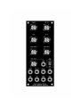
1
Oakley Sound Systems
One of Three
Voltage Controlled Oscillator
Module
PCB Issue 4
User’s Guide
V4.7
Tony Allgood B.Eng PGCE
Oakley Sound Systems
CARLISLE
United Kingdom
Introduction
This User Guide is for the Issue 4 board set only. Check that you have an Issue 4 board. The
issue number is written at the bottom left hand corner of the main board
The Oakley ‘One of Three’ is a voltage controlled oscillator module that was inspired in part by the
VCO design of the later MiniMoogs. In this module I decided to create a VCO that sounded good
and performed well enough to keep up with the digital oscillators of modern day synthesisers.
This is the fourth issue of this popular project and module. The new issue mainly contains
mechanical updates and still features the same powerful analogue sound that won the last three
issues much acclaim.
The VCO features sawtooth, pulse, triangle and a low distortion sine output. The duty cycle of the
pulse output may be controlled directly by a PCB mounted pot, and also an external voltage, the
sensitivity being controlled by another PCB mounted pot. The frequency of the VCO can be
controlled by two PCB mounted pots, one for fine, the other for coarse adjustment. These four pots
are designed to be fitted to the main board, and when special pot brackets are used, the PCB can be
firmly supported to the front panel.
The output levels for the sawtooth, sine and triangle are standardised at +/-5V, ie. 10V peak to peak.
The pulse wave output is also 10V peak to peak, but the peak levels vary with pulse width. The
Oakley VCO uses an interesting technique to maintain the average voltage over one cycle to zero
volts. This new circuit essentially adds an offset to the pulse output to compensate for the non zero
average voltage for any pulse wave that isn't a square wave. Ordinarily, one would see average DC
values varying from +5V to -5V as the PW is swept from one end to the other. In the new VCO, this
average level is kept at zero. This means that for narrow pulses, you now have a wave that goes
from just below 0V [down] to just below +10V [up]. For square waves, you have the usual +5V up
and -5V down. For wide pulses, you have a wave that is just below 0V [up] and just below -10V
[down]. The reason for this is that fast pulse width modulation no longer adds thumping to the
audio output. ie. fast EG sweeps of PW will sound great. Although, no switch is provided to turn
this feature off, you can simply omit one resistor and it will function like other VCOs.
All outputs have an output impedance of roughly 1K.
The pulse output is also switchable between ‘centre modulated’ and ‘edge modulated’ forms of
pulse width modulation. Most VCOs will only offer edge modulated, in which only one edge of the
pulse wave is affected by the pulse width pot or modulating CV. The Oakley VCO allows you to
modulate either one edge (edge) or both (centre). In fixed pulse width applications this generally
makes no audible difference. However, when used with fast moving modulating CVs the difference
in timbre is apparent.
A high impedance synchronisation input is provided to prematurely reset the VCO waveform. With
this you can force the VCO’s operating frequency to that of an external sawtooth signal, say from
another VCO module. This input is level sensitive, so hard sync is possible with inputs of about
+3V or above. Inputs below this will cause only occasional synchronisation leading to interesting
harmonic structures.
Please note; that to cause hard sync effects the master ‘sync’ signal must be a sawtooth (falling
ramp shape) waveform of 10V peak to peak. The slave VCO will not sync to a ramp waveform
which typically has a rising ramp and does not feature the fast rising edge the VCO needs to lock on
to. These ramp waveforms are erroneously called sawtooth by some manufacturers. However, a
simple inverting circuit will be sufficient to turn the waveform around the right way so it can be
used as a sync master.
The VCO supports the standard 1V/octave exponential voltage to frequency relationship. However,
a linear control input is also provided for constant depth frequency modulation.
Temperature compensation is performed by using a matched transistor pair in the exponential
convertor, and a high quality temperature sensitive resistor.
The Oakley CV/gate bussing
You really should think about it if you have a medium sized Oakley system. Using the Oakley
Dizzy board, it allows Keyboard CV and Gate signals to be piped around the back of the modular’s
case along with the power supply rails. Any VCO and VCF can be connected to the KEY-CV line,
and this will save you having to patch KEY-CV to every module that needs it. Inserting any patch
lead into the 1V/OCT socket will override the CV bus line connection. The gate signals are treated
similarly to the CV line but for use with the ADSRs and other EG modules.
The Oakley CV/gate buss uses a common three way 0.1” header to carry the two signal lines. A
third, as yet unused connection is also present for future expansion.
The new VCO issue supports the Oakley CV/gate buss natively. Previous issues had the CV buss
being connected to the module via a wire tail attached to the 1V/octave socket’s normally closed
(NC) lug. The new socket board features an optional three way header that can be fitted to allow
direct connection to the CV/gate buss on an installed Oakley Dizzy system. If not required the
header can simply be omitted altogether and a solder link put in its place. Or, the header can be
fitted and a simple two way jumper, like those used on computer motherboards, can be fitted to
allow to the buss to implemented at a later date.
The Issue 4 PCB set
The main PCB is 108 mm (depth) x 143 mm (height) in size. All three boards use double sided
copper traces and have through plated holes. The solder pads are large and are easy to solder and
de-solder if necessary. They have a high quality solder mask on both sides for easier soldering, and
have clear legending on the component side for easier building.
If you are building the standard design there are no components mounted off the boards. All
components including sockets and pots are soldered directly to the boards.
Previously, many Oakley modules have had the sockets, switches and extra pots wired to the board
by individual wires. This module allows all the socket wiring to be done via the socket PCB and
two MTA solderless or Molex connections. If you are building this module in the standard Oakley
format this new system will reduce assembly time and possible wiring errors.
Some people will wish to use this Oakley design in a non standard format, such as fitting it to
another manufacturer’s rack or one of their own invention. This is perfectly easy to do. Simply do
not use the socket board and wire the main board to the sockets as per usual.
I have provided space for four of the control pots on the main PCB, whilst the other three pots are
fitted to their own board. If you use the specified pots and brackets, the PCBs can be held firmly to
the panel without any additional mounting procedures. The pot spacing is 1.625” and is the same as
vertical spacing of the MOTM modular synthesiser.
There are detailed instructions later in the document about how to build the boards. The whole
project takes around 3 hours to build and test.
Oakley VCO Issue Changes
For those interested the Oakley VCO has evolved slowly over the last nine years:
Issue 1: The start; the VCO is based primarily on the third series Minimoog VCO with plenty of
additions. eg. in built 10V reference, sync, different exponential convertor and summing stage,
sinewave output, pulse width selection, output buffering, Omeg pots.
Temperature compensation was generally provided by a +3000ppm/K 900mW film resistor. This
was later upgraded to the KRL wirewound types for last ten or so boards that were sold.
Issue 2: Boards had the following features added:
Added -10V reference to go with the +10V internal reference voltage already on issue 1. This
stabilises absolute pitch drift so that supply rail potential doesn't affect the pitch of the VCO. All
pitch pots use the +/-10V references.
The range of the TUNE trimmer was reduced and this was coupled with a reduction in the quiescent
operating frequency.
Added SYNC input buffer circuit. This has the advantage of providing a high impedance input. The
old issue had a 10K input resistance which caused a slight drop in amplitude to the other (master)
VCO connected to the SYNC input. An additional benefit is that unwanted cross coupling between
two or more slave VCOs was eradicated. With the older VCOs, any two slave VCOs tended to sync
to each other as well as the master. Interesting effect though.
I swapped the positions of the power supply regulator with the CV summer circuitry. This enabled
me to move the two tuning multiturn trimmers to the edge of the board. The old issue 1 board had
these parts in the centre of the PCB, and they were impossible to trim when the board was fitted
into the Oakley Orbital monosynth. Moving the trimmers to the edge means that we can now use
side adjustable trimmers in the Orbital to facilitate easy tuning with the boards in situ. This does not
affect the modular set up in any way, in that we will continue to use top adjustable trimmers as
before. As it turns out, no issue 2 boards ever made it into the Orbital project.
The pitch spacing of the polyester capacitors was changed from 0.3” to 5mm. This was in line with
other Oakley boards.
Added separate triangle and sine wave offset trimmers. This meant that switching to centre on the
PWM source switch would not affect the mark-space ratio of the square wave output.
Issue 3: Boards had the following features added:
Sinewave purity increased.
Two high frequency tracking compensation networks instead of just one. The standard Sergio
Franco technique, used on the earlier issues, is now fixed to compensate only for the FET discharge
time. Dave Rossum's technique for compensating for the bulk emitter resistance (Rbe) of the NPN
pair is now added with variable depth controlled by the new HFT trimmer.
Constant zero average output voltage from the pulse wave. This is achieved by considerable
changes to the older simple design.
The board has four Spectrol pots instead of three Omeg ones. This makes the board less cramped
since the board is now longer. The solder pads for the jack sockets now are on standard sized solder
pads. 0.1" headers are still provided for those of you who like them, although the main reason for
keeping these is the Orbital. The new board layout required a new modular faceplate to be made for
the module.
Issue 4: Boards had the following features added:
Major mechanical changes. The module is now constructed from three PCBs and features solderless
interconnects. This facilitates easy construction. The board set can still be used with the issue 3
front panel design.
Spectrol 248 pots are now used throughout the module.
Change to the high frequency tracking (HFT) circuitry to include Rene Schmitz’s improved take on
the Rossum method of compensating for Rbe.
Change to the way the fine tune pot’s CV was handled. The single metal film 10M resistor was
replaced by a simple resistor network. 10M 1% resistors are getting hard to come by these days.
Replaced the now deleted CA3080 from the sine shaping circuitry. The new board simply uses one
half of an LM13700 device.
Easy to fit to the Oakley CV/gate buss using an optional three way header fitted to the new socket
board.
Latest PCBs are Ni/Au finish and are RoHS compliant.
Power Supplies
The design requires plus and minus 15V supplies. These should be adequately regulated. Although
quite large perturbations in the supply will not cause any pitch changes, waveform linearity and DC
offset will be affected by an unregulated supply. The current consumption is about 30mA per rail.
Power is routed onto the PCB by a four way 0.156” MTA or Molex type connector. You could, of
course, wire up the board by soldering on wires directly. The four pins are +15V, ground, panel,
-15V. The panel connection allows you to connect the metal front panel to the power supply’s
ground without it sharing the modules’ ground line. More about this later.
Circuit Description
The VCO circuit can be thought of as several little subsections connected together. Lets look at
these little sections separately.
The first thing to look at is the power supply. This is shown on the bottom of the second sheet of the
schematics. The VCO could have been powered by +/-15V, but I wanted the VCO to sound like a
minimoog. To do this, I have used the same voltage levels within the VCO core as the original.
Thus we need to generate stable +10V and +5V supplies. I still used the +/-15V supply for most of
the op-amps as this would not have any affect on the waveforms.
Power enters the board on a 4-way Molex connector. It is filtered initially by two small ferrite
inductors, and decoupled by C20 to C23. These prevent stray high frequency pulses from entering
or leaving the unit by the power supply lines. A LM723 voltage regulator IC is used to provide the
10V. This is an old IC design, some 30 years, but it is a superb device and has very low noise. The
only problem is that you have to set the output manually. PSU is a trimmer to set the voltage to be
exactly 10.00V. The PCB has been laid out for a cermet trimmer for long term stability.
Additional power supply decoupling is provided to each set of op-amps and ICs. This prevents any
reset pulses from travelling down the power supplies and soft synching the other VCOs in your
system.
To find the next part of the power supply we need to look at the first sheet of the schematics. Two
sections on this page generate the stable +5V and -10V required by the VCO.
U2 (pins 5, 6, 7) provides the +5V supply, by simply buffering half the +10V rail. An LT1013 is
specified to provide a very stable output.
U3 (pins 1, 2, 3) is a simple inverter circuit that produces a very stable -10.00V supply for the tune
pots and trimmers. Together with the stable +10.00V supply, this prevents any perturbations in the
+/-15V supply rails from affecting the tuning of the VCO. In reality, the tolerance of the 22K
resistors may mean that the output is not exactly -10.00V. This is perfectly OK, since we are not
interested in the actual value so much, but the stability. Those 22K resistors are metal film and their
value will not change appreciably over the years or at differing temperatures.
The VCO’s pitch is determined by a variety of sources. Two 1V/octave CV inputs, and two pots on
the front panel, and a trimmer to set initial frequency. U2 (pins 1, 2, 3) is built as a voltage summer.
It takes the voltages from the five sources and adds them together. The gain of the summer is set by
the input resistors and R44 and the V/OCT trimmer. For the two 1V/octave inputs the gain is
roughly -0.7. The V/OCT trimmer is adjusted to give a rise of one octave in output frequency when
the keyboard input voltage goes up by 1V. The output of the CV summer is then fed to the
exponential convertor via R29 and R30.
The exponential convertor is based around on half of U3 (5, 6, 7) and the matched NPN pair of U4.
Its output is a current that is proportional to the exponent of the voltage applied at the base of the
left hand transistor of U4. The circuit gives the VCO a sensitivity of roughly -18mV/octave, so R29
and R30 reduce the output of the CV summer to this level. However, it is worth noting that R30 is a
temperature sensitive resistor. The resistance of R30 will go up with temperature at a rate of 0.33%
for every degree Celsius. This should counteract the temperature effects produced by the
semiconductor junctions in U4. To get the best temperature stability R30 is mounted right on top of
U4. This way the temperature of the two devices should be the same.
It is possible to get an exponential response from a single transistor, but that has problems as Vbe,
the junction voltage, changes with ambient temperature. The ‘temp co’ resistor cannot compensate
for this change in the transistor’s operating current. So the now classic circuit with two perfectly
matched transistors and an op-amp, U4 and U3, is used. Changes in the Vbe for one half of the
transistor pair are mirrored in the other. The op-amp then matches the current in the first transistor
with the same current in the other one. So the collector current in the first transistor will effectively
control the collector current in the second. And it is the current drawn by the second transistor that
controls the frequency of the VCO.
The op-amp method also has another bonus, it allows an additional current to be injected into the
inverting pin of U3. This current will directly control the output current of the exponential
convertor. R15 allows an input CV to control this current. We now have a linear frequency
modulation input, whose sensitivity is set by R15. Connecting this input to the wiper of a pot,
allows you to control the sensitivity of this input directly from the VCO’s front panel.
Note that this input is not a true linear input control. This VCO, and most other modular VCOs,
don’t have that capability. What we have here is a constant modulation index input. This is linear
modulation, but not linear control. The precise description of this statement is probably beyond the
scope of this document, but in a nut shell it means this: The linear input will not act with a strict
volt per hertz relationship. That is, for every 1V, the output frequency will not rise by a fixed
amount. But it will act so that audio rate FM will create a constant depth of modulation on any
given frequency controlled by the usual 1V/octave inputs. This means that the for audio rate FM
effects (clangs, bells and the like) you can get very good results with the linear FM input.
R3 has been chosen to set the operating frequency of the VCO at approximately 1kHz when the
voltage at the base of the left hand transistor is zero. The exponential convertor works at its most
accurate when the voltage across the two bases is zero. And since the human ear is particularly
sensitive to frequency changes at around 1kHz it is good to make the most accurate part of the VCO
at this frequency.
The output of the exponential convertor is a current. It is this current that controls the core of the
oscillator. Contrary to many people’s ideas, the core of a VCO is typically a linear CCO. That is a
current controlled oscillator. A doubling of current to (or from in this case) the CCO will produce a
doubling of output frequency.
The core of this VCO is a traditional sawtooth oscillator. C14 is the timing capacitor that is charged
by the output of the exponential convertor. Since one end of C14 is tied to +5V, the voltage at the
other side of C14 moves towards zero volts as current is ‘sucked’ out of it. The higher the current
the faster the voltage drops. This voltage is ‘sniffed’ by one half of dual op-amp U5, which
produces a replica of this voltage at its output. Q4 aids the output of U5, as well as providing a
suitable offset for the triangle generator circuit (see later).
U7 (pins 1, 2, 3) is a comparator, and it is ‘watching’ the output of U5. When the voltage across
C14 reaches -5V, the output of U5 (pin1), normally at -15V, suddenly flies upward towards 10V.
This sudden level change passes through C13, and turns on JFET, Q3. This rapidly shorts out C14,
and the voltage across the capacitor drops to zero and both of its pins are at +5V once again. This
means that the voltage at the input of U8 is also at +5V, and the charging process begins again. C10
controls the time that the FET is on.
The sync input enables an external voltage to trip the comparator early. This will cause premature
shorting of the capacitor, locking the fundamental of the VCO to an incoming external sawtooth
signal. However, the fall time of the VCO’s saw waveform will still be set by the input CV to the
VCO. Thus, you will not get traditional sawtooth waveforms, but half completed sawteeth. The
sonic affects of these are marvellous, especially if you sweep your VCO with an envelope generator
whilst locked to another VCO at fixed frequency. The controlled VCO is often called the ‘slave’,
while the fixed VCO is called the ‘master’.
The incoming sync signal is first buffered by Q1, a simple emitter follower. This is shown on the
second page of the schematics. R11, C1 and C2 provide decoupling to prevent power supply noise
from accidental triggering of the VCO. The buffered signal is then passed to a simple differentiator
based around C9 (back on page one again). This part in conjunction with D3 and R24 only allow
only fast moving rising edges of the input waveform to reset the VCO core. In theory this should
allow any pulse wave to be used as sync waveforms, but the best sync sounds can be obtained when
a falling sawtooth master signal is used.
This last statement is very important if you want to use sync effectively. Use sawtooth outputs from
Oakley VCOs to sync other Oakley VCOs. MOTM VCOs produce rising ramps not falling
sawtooth waveforms. So you if you want to use a MOTM VCO as the master to sync the slave
Oakley VCO, then you must invert the MOTM’s output first. You could use an Oakley MultiMix to
do the inversion.
The suggested layout of the Oakley VCO includes a depth control for the sync input. This will
allow you to create partial synching effects. This effect is very difficult to describe in words and has
to be heard to be believed. But very very complex timbres can be produced this way.
At high frequencies the VCO can go a little flat due to the finite time it takes to reset C14, and
errors in the exponential convertor. By lowering the maximum peak voltage of the sawtooth
waveform, the capacitor has less charge to loose before the output of U5 reaches zero. Thus the
frequency is higher than it would have been. Using a resistance in series with C14, we have a
voltage drop developed across the resistor that increases with frequency, due to the increased
current through the exponential convertor. This method was first postulated by Sergio Franco, and
is usually called ‘Franco’ compensation because of this. This works very well, but it does mean that
the amplitude of the sawtooth waveform decreases slightly with increasing frequency. In the first
two VCO issues I made this resistor variable. I was using the Franco resistance to compensate for
both reset time and errors in the exponential convertor. In the issue 4 VCO, this resistance was fixed
by R37, and is compensating for reset time only.
The exponential convertor causes errors due to ‘bulk emitter resistance’ or Rbe in the NPN pair.
The SSM2210 is a very good matched pair with low values of Rbe, but it still has an effect at very
high frequencies of the VCO. Rbe is not a real resistor, but it acts as if a resistor was connected in
series with the emitter of the transistor.
In the early issue VCO boards, this loss of high frequency performance was cancelled out by the
effect of the Franco resistor. But really, this is a bit of a cludge since the Franco is designed to
compensate for a fixed timing error (the FET reset time), whilst Rbe causes an error related to
frequency. Over the limited range of an audio VCO, this is usually perfectly OK and Franco is used
in many commercial synth VCOs as the only high frequency compensation technique. For issue
three I decided to go one better. The newer issue VCOs use a fixed Franco resistor for the reset
time, and also use the Rossum technique to compensate for the exponential generators error.
Dave Rossum, founder of E-Mu systems in the 1970s, was an important player in the development
of the SSM chips. The SSM2030 VCO chip, which was not as good in comparison to the later
Curtis CEM3340, was groundbreaking when it came out. Dave’s method of HF compensation for
the SSM2030 involved gently pulling the base of the first transistor of the NPN pair lower when the
collector current through the second NPN gets bigger.
In the issue 3 VCO I slavishly copied Dave’s idea as presented in Electronotes and indeed the
Prophet V many years ago. However, due to work done recently by René Schmitz this simple
method can be improved upon with the same number of components. As in the original Rossum
idea a fixed emitter resistor, R17, can be used to effectively measure the emitter current, since the
voltage on its bottom end will fall as collector current rises. Previously we took this voltage, passed
it through a diode to compensate for the base-emitter voltage drop (Vbe) of the matched pair and
then fed a small proportion of the resultant voltage back to the base of the left hand transistor. This
works well enough.
However, René’s idea improves on this on two counts. Firstly, the diode in the pure Rossum
method doesn’t exactly compensate for the Vbe because the current flowing in the diode and the
base-emitter junction are different. In the new circuit, both semiconductors see the same current as
they are fed from identical resistive sources; R17 and the HFT trimmer are both the same value.
Therefore, the voltage drop across D2 and Vbe should track each other reasonably well, even over a
change in ambient temperature. Secondly, the new method feeds the base of the left hand transistor
with more or less the same resistance. That is the extra resistance due to the HFT circuitry the left
hand transistor base ‘sees’ is pretty much fixed at the value of R20 only. Thus altering the HFT
trimmer should not result in a change in the overall operating frequency of the VCO as it did in the
old method.
Ideally the diode should be matched with the transistor array. However, HFT compensation due to
Rbe is only a small consideration at audio frequencies so we need not get too bogged down with the
higher orders of errors.
Going back to the VCO core: The sawtooth output from U5/Q2 is amplified by the other half of U5
(pins 5, 6, 7), before being sent to the output pad. The final output is roughly +5V to -5V, ie. 10V pp.
The triangle shaper is essentially a full wave rectifier, whose operating point is about 2.5V. If the
operating point is not exactly half the peak value of the sawtooth output of U5, then the triangle
wave will have discontinuities in it. This leads to a slightly brighter or harsher sound than the
perfect ‘textbook’ triangle waveform. SHP-T is a trimmer that allows precise enough adjustment in
the operating point to eliminate these glitches.
The created rectified wave is filtered before amplifying and level shifting by U6. The SYM-T
trimmer sets the DC offset of the wave output to match that of the sawtooth output. The final output
is again 10V p-p.
The sine wave shaper circuit, shown on page two of the schematics, acts upon the triangle wave
output. The rounded peaks of the sinewave are created by deliberately overdriving the inputs of one
half of U8, a dual operational transconductance amplifier (OTA). These devices are normally used
as VCAs, but in this VCO it is merely acting as a soft clipping unit. The non linearities of the
OTA’s input stage being utilised to squash the top and bottom peaks of the triangle wave input. The
gain of the shaper is fixed with R32 and R48. SHP-S adjusts the amount of overdrive. Since U8
gives a current output, it must be turned into a voltage and this is done by U9 (pins 5, 6, 7).
R18 provides a special negative feedback path within the shaper circuit. This increases the nonlinearity of the whole stage at the critical peaks of the output waveform.
SYM-S provides compensation for the OTA’s own offset voltage. This offset voltage means that
the OTA will soft clip asymmetrically. By adding a small voltage of the opposite polarity to one of
the input pins, we can cancel the effects of the offset.
The sine wave created by this process does not give us a perfect textbook example of a sine wave.
However, the wave is very low in harmonics and for musical uses it is adequate.
The final output, and the final circuit block is the pulse conditioner. This is also found on page two
of the schematics. The first section of this is the CV summer and is based around U9 (pins 1, 2, 3).
This circuit simply sums together the PWM (pulse width modulation) CV input and the voltage
from the wiper of the Width pot. The output of the CV summer will go from around -5V to +5V
when being controlled by the Width pot alone.
The pulse wave generator itself is based around the second half of the comparator, U7 (pins 5, 6 &
7). This compares either the triangle wave or sawtooth wave output with a voltage set by the output
of the CV summer. If the waveform is higher than the voltage from the CV summer, the
comparator’s output goes low. If it is lower, the output goes high. Thus, the output is either low or
high, and spends very little time in between. This creates a rectangular waveform, where the
proportion of time spent high or low is controlled by the WIDTH pot and/or the external CV. If the
width pot is set to its middle position, and no input CV is applied, the output waveform should be a
square wave. The output of the comparator swings from -15V to ground (or zero volts).
The output of the comparator is out of phase with the audio input. Q2 inverts this signal, so that the
generated pulse wave will go high when the saw or triangle wave is high. It would be possible to
generate the correct phase by simply wiring the comparator’s inputs pins differently. Thus you
wouldn’t have to invert the output since it would already be the right way around. Earlier issues of
the VCO, in fact, did this. However, this caused a less than perfect output waveform. The positive
feedback provided by R40, which is needed for good comparator action, would cause the sawtooth
or triangle wave to be superposed to the output waveform. This was considered not to be a problem,
but with the new issue I decided to do things differently. And perhaps more correctly.
What follows after the comparator is, I think, new to modular VCO design. The inverted output of
the comparator is now summed with two voltages in U9 (pins 12, 13 &14). One comes from the
+15V supply via R74. The other is the output of the CV summer. The former allows the -15V/0V
output swing of the comparator to be normalised between +5V and -5V. The other allows the output
to be offset against zero volts as the pulse width is varied. When the CV summer has zero volts at
its output, the generated pulse waveform is a square wave. No additional offset is added and the
waveform from U9’s output moves between +5V and -5V. As the pulse width changes, then the
output of the CV summer moves away from zero. This is added to the waveform and the pulse
output waveform moves above or below zero volts.
Analysing this dynamically changing output reveals that the average output voltage is actually
always zero. This is because the offset added compensates for the altering amounts of time the
waveform spends in the high (or low) states.
The summing circuit also inverts the waveform, so once again, we create the wrong phase. A simple
op-amp invertor circuit, U9 (pins 9, 10 & 11) turns the pulse wave the right way round again.
If you do not want this dynamically varying output signal, then all you need to do is omit R71.
The source of the audio source for the comparator comes from either the triangle or sawtooth
waveforms. This selection is another unique feature of the Oakley ‘One of three’ VCO. Both will
sound the same with fixed pulse widths. But, they do sound different when the width CV is
modulated quickly.
Components
Most of the parts are easily available from your local parts stockist. I use Rapid Electronics, RS
Components and Farnell, here in the UK. The VCO module was designed to be built mostly from
parts obtainable from Rapid Electronics and ourselves.
The resistors can be 5% carbon 0.25W types except where stated. However, I would go for 1%
0.25W metal film resistors throughout, since these are very cheap nowadays. If you do want to use
5% types, the please note that some of the resistors have to be 1% or better types. Failure to use
good quality parts in these locations will affect the tuning stability of the VCO. These critical parts
are indicated in the parts list.
Some of you may want to use 0.1% precision resistors in these critical positions. These are quite
pricey and may be best to use in the most critical positions only. These would be: R32, R44, R29. It
is my opinion that this is not worth doing and that 1% types are perfectly adequate.
All the electrolytics (abbreviated to ‘elect’ in the parts list) should be 25V or 35V, except where
stated, and radially mounted. Don’t chose too high a voltage. The higher the working voltage the
larger in size the capacitor. A 220V capacitor will be too big to fit on the board. 35V is a good value
to go for.
The pitch spacing of all the non-polar capacitors is 5mm (0.2”). This may differ from some of the
older Oakley boards you have built.
The polyester capacitors are actually metallised polyester box types. These have a lead pitch of
5mm (0.2”) and come in little plastic boxes in a variety of colours. Typical working voltages will be
63V, 100V or even 400V. They key thing to look out for is physical size and lead pitch. Most of
Rapid’s are either 63V and 100V and all will fit on the board.
The ceramic capacitors should be ‘low-K’ ceramic plates. These are sometimes called C0G types.
The lead spacing is 0.2” or 5mm. Do not chose cheap and nasty ceramic types, usually ‘high-K’,
obtainable from some surplus places. These can lead to a noisy audio output. Alternatively, you can
use polyester parts in place of the larger values of ceramics.
C14 is a close tolerance (2% or better) polystyrene capacitor or better. The PCB is laid out for
EXFS/HR series made by LCR. Farnell and others sell these. They are good components at a good
price.
The matched pair, SSM2210P, can be difficult to trace, although Farnell and RS-Ltd do carry stock.
You can use the LM394 or MAT-02 instead. You could also match your own pair from discrete
transistors, but thermal matching is very hard to do.
U2 and U3 are both good dual op-amps. The LT1013CP from Linear Technology is an ideal part. I
used to recommend the OPA2277 but we now know of one case where a particular batch of
OPA2277 caused oscillation to the +5V reference voltage
The LM1458 is a real oldie, and some places don’t stock it any more. In the UK, Farnell and RS sell
the little chap for peanuts.
The LM13700N may be substituted with either the older 13600 (still made by JRC) and the now
defunct Phillips’ NE5517.
All ICs are dual in line (DIL or DIP) packages. These are generally, but not always, suffixed with a
CP or a CN in their part numbers. For example; TL072CP. Do not use SMD, SM or surface mount
packages.
The BC550 or BC549 devices are discrete low noise transistors. Quite often you see an A, B or C
suffix used, eg. BC549C. This letter depicts the gain or grade of the transistor (actually hfe of the
device). The ‘One of three’ VCO is designed to work with any grade device although I have used
BC550 throughout in my prototypes.
The positive temperature coefficient (PTC) resistor is worthy of a mention. Meggitt make a
+3000ppm/K type that is a very good part. It is available from Farnell and the part number is 732278. However, the actual theoretical value of compensation should be closer to around
+3500ppm/K when used in the circuit that I have chosen. The Meggitt part thus falls slightly short
of this, and may cause the VCO to lose ‘V/oct’ tracking over the full keyboard range unless the
ambient temperature is pretty stable.
It is therefore preferable to get something closer to the ideal value. The ones I recommend are 1W
wirewound resistors with a nominal TC of +3500ppm/K. You can buy these from us, KRL-Bantry
in the US, or from Senso's Vintage Planet (www.senso.dds.nl/index.html). These are sold as
equivalents to the old Tel Labs Q81 series. Once fitted to the VCOs, they give better tuning stability
and allow the modular to ‘warm up’ quicker. They are also physically larger than the Meggitt type
which means they are more stable in air drafts too.
The PTC resistor is fitted to the board so that it lies across the top of the SSM2210. A bit of thermal
compound (eg. Thermpath) could be used to keep the two devices in contact. You’ll need to
carefully bend the legs of the TC to make sure it lies flat on the surface of the 2210 and still fits
through its solder pads.
The JFET is the J112, this is very common and is the same FET die as the original MiniMoog. But
take note, the Mini used the E112, and that has a different pin out. Some US customers have found
the J112 quite difficult to trace. However, it can be found at Radio Shack.
The board mounted pots are Spectrol 248 series with Oakley pot brackets. You could use any type
you want, but not all pots have the same pin spacing. Not a problem, of course, if you are not fitting
them to the board.
We carry a stock of all the pots you need as the VCO pot kit. One thing to note if you are buying
knobs for these pots. The older Oakley modules used Omeg pots which come with a 6mm shaft,
while the Spectrol ones have a 6.35mm shaft.
The toggle switch is a standard SPDT (single pole, double throw) switch. The types I use are made
by APEM in France, and have a flat toggle. RS-Components Ltd (320-916) and Farnell (1082301)
sell them in this country at a very good price.
L1 to L2 are leaded ferrite beads. These are little axial components that look like little blackened
resistors. They are available from most of the mail order suppliers. Find them in the EMC or
Inductor section of the catalogues. Farnell sell them as part number: 9526820.
The multiturn trimmers are the ones that have the adjustment on the top of the box. Spectrol and
Bourns make these. Some types are 22 turns, while others are 25 turns. Either will do. They should
have three pins that are in a line at 0.1” pitch. Don’t chose the 10-turn ones with the adjustment on
the end, they won’t fit on the PCB.
The four trimmers, SYM-S, SYM-T, SHP-S and SHP-T, are standard sealed carbon units. These are
adjusted from the top and, as such, are called horizontally mounted types. Piher and other
companies make suitable types. Lead spacing is 0.2” for the track ends, and the wiper is 0.4” above
a line joining the other two pads. I use Iskra ones available from Rapid.
The PSU trimmer is a special single turn cermet type. This type of trimmer has a different PCB
footprint than the other types. Lead spacing is 0.2” for the track ends, and the wiper is 0.2” away
above a line joining the other two pads.
The eight way jumper interconnect is a one piece assembly bought ready made from several places.
I buy mine as an eight way 55 mm or 85mm long piece. These come as pre-stripped and even tinned
with solder too. Make sure you get the 0.1” (2.54mm) pitch variety. The Rapid part number is 221650 for the 55mm and 22-1655 for the 85mm one.
For the 0.1” interconnections I use the 26 awg MTA parts. These are made by Amp, now part of the
massive Tyco empire. To use these effectively you need a special tool to poke the wires into the
special ‘housings’ The housing contains specially shaped contacts that cut through the insulation of
the wire so you don’t need to do any stripping. Just simply push down on the wire with the tool to
lock it into place in the housing.
You can also use Molex strip and crimp systems. More about this one later on.
Name
Farnell Part number
Amp’s part number
Four way housing
Four way header
Five way housing
Five way header
Six way housing
Six way header
1098712
588593
1098713
588600
1098714
588611
640442-4
640456-4
640442-5
640456-5
640442-6
640456-6
Handtool
589494
59803-1
Input and output sockets are now board mounted in the standard module assembly. You could of
course use any types if you would like to wire your sockets up with individual wires.
I use the Switchcraft 112A 1/4” sockets in all my ready made modules. These excellent parts are
also used on the Moog and MOTM modulars. The version you need to fit in the socket board is the
112APC. This part is stocked by most suppliers. Both Rapid and Farnell sell is at a reasonable
price. Rapid also sell a Far Eastern clone of the 112APC part that is considerably cheaper, but
doesn’t look as nice. Please note that the standard 112A will not fit easily into the boards as it has
solder tags.
Finally, if you make a change that makes the circuit better, do tell the ‘Oakley-synths’ mailing list
or myself directly. Any updates are added to the current user guide as quick as possible.
UK builders should know that there is a ‘Oakley Preferred Parts List’ online which is updated
periodically by myself. This can be found at www.oakleysound.com/parts.pdf.
VCO issue 4 Parts List
A quick note on European part descriptions. To prevent loss of the small ‘.’as the decimal point, a
convention of inserting the unit in its place is used. eg. 4R7 is a 4.7 ohm, 4K7 is a 4700 ohm
resistor, 6n8 is a 6.8 nF capacitor.
Resistors
All 5% carbon 1/4W or better. Components designated as 1% should be 0.25W 1% metal film or
better.
22R
100R
390R
470R 1%
1K
1K +3500ppm/K Temp co.
2K
2K2
2K2 1%
5K1
5K6
6K2
6K2 1%
8K2
10K
10K 1%
18K
22K
22K 1%
33K
39K
39K 1%
47K
56K
62K
68K
68K 1%
100K
100K 1%
150K
180K 1%
220K
270K
390K
390K 1%
680K 1%
750K
1M
1M 1%
R50, 42, 41, 60, 7, 75
R11
R19, 23
R37
R55, 62, 24, 56, 39, 67
R30
R17, 25
R5
R22
R68
R65
R59
R21
R16, 69
R80, 78, 27, 70, 66, 48, 46, 49, 35, 10, 34
R2, 57, 58
R79
R82, 73, 9, 71
R4, 6
R72, 77, 76
R47
R29
R12, 33, 54
R63
R18, 81
R74
R44
R36, 38, 13, 15, 61, 52, 51
R1, 32
R64
R28
R8
R53
R14, 20
R40
R3, 45
R83
R26, 84, 43
R31
Capacitors
100nF 63V polyester
100pF Low-K ceramic
10uF, 25V elect
18pF Low-K ceramic
1nF 100V polyester
1nF 1% polystyrene
220pF low-K ceramic
22uF, 25V elect
4u7, 35V elect
470pF low-K ceramic
C11, 12, 2, 23, 22
C13, 16
C3
C10
C4
C14
C9
C15, 5, 7, 17, 6, 19, 24, 26, 1
C18, 20, 21
C8, 25
Discrete Semiconductors
1N4148 signal diode
BAT42 Schottky diode
BC550 NPN transistor
J112 J-FET
D2, 4
D3
Q1, 2, 4, 5 (You can use the BC549 too)
Q3
Note: there is no D1.
Integrated Circuits
LM1458 dual bi-polar op-amp
LM13700 transconductance amp
LM2903 dual comparator
LM723 voltage regulator
LT1013CP low drift dual op-amp
SSM2210P matched NPN pair
TL074 quad bi-fet op-amp
TL072 dual bi-fet op-amp
U6
U8
U7
U1
U2, U3
U4
U9
U5
Trimmers
100K multiturn trimmer
10K multiturn trimmer
2K multiturn trimmer
1K horizontal carbon trimmer
1K cermet trimmer
22K horizontal carbon trimmer
47K horizontal carbon trimmer
TUNE
V/OCT
HFT
SHP-T
PSU
SHP-S
SYM-S, SYM-T
Pots
50K Linear Spectrol 248 pot
Oakley/Spectrol pot brackets
Spectrol nuts
DEPTH, WIDTH, TUNE-2, TUNE-1 on main board
EXP, LIN, SYNC on pot board
7 off for the above
7 off for the above
Miscellaneous
SPDT toggle switch
PWM type
1 off
4-way 0.156” MTA header
PWR
1 off
3-way 0.1” header
Oakley Buss optional connector
1 off
4-way 0.1” MTA header
4-way 0.1” MTA housing
MAIN-2 (Main PCB and socket PCB)
MAIN-2 cable
2 off
2 off
5-way 0.1” MTA header
5-way 0.1” MTA housing
POTS (Pot PCB and socket PCB)
NSE cable
2 off
2 off
6-way 0.1” MTA header
6-way 0.1” MTA housing
MAIN-1 (Main PCB and socket PCB)
MAIN-1 cable
2 off
2 off
8-way jumper lead
LINK interconnect
1 off
Leaded ferrite beads
L1, L2
You may well want to use sockets for the ICs. I would recommend low profile turned pin types as
these are the most reliable. You need two 14-pin DIL sockets, and seven 8-pin DIL sockets.
Populating the Main Circuit Board
Oakley PCBs are supplied with a RoHS compliant finish. This is a high quality finish but does
possess slightly different soldering characteristics to the traditional lead based HASL finish. Handle
the boards with care, and avoid touching the solder plating since this can cause premature tarnishing
of the finish. Shelf life is hard to predict but we recommend soldering in all the components less
than one year from when you receive your board.
Neither I nor Paul Darlow are responsible for any accidents caused whilst working on these
boards. It is up to you to use your board responsibly and sensibly.
Occasionally people have not been able to get their Oakley projects to work first time. Some times
the boards will end up back with me so that I can get them to work. The most common error with
most of these was parts inserted into the wrong holes. Please double check every part before you
solder any part into place. Desoldering parts on a double sided board is a skill that takes a while to
master properly.
If you have put a component in the wrong place, then the best thing to do is to snip the component’s
lead off at the board surface. Then using the soldering iron and a small screwdriver prize the
remaining bit of the leg out of the hole. Use wick or a good solder pump to remove the solder from
the hole. Filling the hole with fresh solder will actually make the hole easier to suck clean!
Sometimes people like to substitute parts in place of my own recommendations. Feel free to do this,
but remember that there is normally a good reason why I have selected that particular part. If you do
find that, say changing an op-amp with another one, makes an improvement, please do let me know
either via the Oakley-Synths list or directly to me.
All resistors should be flat against the board surface before soldering. It is a good idea to use a ‘lead
bender’ to preform the leads before putting them into their places. I use my fingers to do this job,
but there are special tools available too. Once the part is in its holes, bend the leads that stick out the
bottom outwards to hold the part in place. This is called ‘cinching’. Solder from the bottom of the
board, applying the solder so that the hole is filled with enough to spare to make a small cone
around the wire lead. Don’t put too much solder on, and don’t put too little on either. Clip the leads
off with a pair of side cutters, trim level with the top of the little cone of solder.
Once all the resistors have been soldered, check them ALL again. Make sure they are all soldered
and make sure the right values are in the right place.
The diodes can be treated much like resistors. However, they must go in the right way. The cathode
is marked with a band on the body of the device. This must align with the vertical band on the
board. In other words the point of the triangular bit points towards the cathode of the diode. When
all the diodes are in place, double check all are pointing the right way.
The polyester film capacitors are like little blue boxes. Push the part into place up to the board’s
surface. Little lugs on the underside of the capacitor will leave enough of an air gap for the water
wash to work. Cinch and solder the leads as you would resistors.
The ceramic capacitors are strange flat plates made from pot. Be careful with these and make sure
you have bought the ones with 0.2” lead spacing. Forcing the smaller 0.1” ones into these larger
pads will break them. Another thing to watch out for is the identification markings on these
capacitors. For example n47 is actually 470pF.
The smaller electrolytic capacitors are very often supplied with 0.1” lead spacing. My hole spacing
is 0.2”. This means that the underside of these radial capacitors will not go flat onto the board. This
is deliberate, so don’t force the part in too hard. The capacitors will be happy at around 0.2” above
the board, with the legs slightly splayed. Sometimes you will get electrolytic capacitors supplied
with their legs preformed for 0.2” (5mm) insertion. This is fine, just push them in until they stop.
Cinch and solder as before. Make sure you get them in the right way. Electrolytic capacitors are
polarised, and may explode if put in the wrong way. No joke. Oddly, the PCB legend marks the
positive side with a ‘+’, although most capacitors have the ‘-’ marked with a stripe. Obviously, the
side marked with a ‘-’ must go in the opposite hole to the one marked with the ‘+’ sign. Most
capacitors usually have a long lead to depict the positive end as well.
IC sockets are to be recommended, especially if this is your first electronics project. Make sure, if
you need to wash your board, that you get water in and around these sockets. And that any water is
thoroughly dried out before you power up. Sockets harbour little pools of water in their pins which
can lead to some very odd effects. Several sharp taps face down onto a towel will loosen off any
remaining globules of liquid.
The transistors are all in the same type of packaging and therefore look the same. Only the numbers
on the side will allow you to tell them apart. Match the flat side of the device with that shown on
the PCB legend. Push the transistor into place but don’t push too far. Leave about 0.2” (5mm) of the
leads visible underneath the body of transistor. Turn the board over and cinch the two outer leads on
the flip side, you can leave the middle one alone. Now solder the middle pin first, then the other two
once the middle one has cooled solid.
Sometimes transistors come with the middle leg preformed away from the other two. This is all
right, the part will still fit into the board. However, if I get these parts, I tend to ‘straighten’ the legs
out by squashing gently all the three of them flat with a pair of pliers. The flat surface of the pliers
parallel to the flat side of the transistor.
There are three types of trimmer used in this project. In two of these types we are actually using two
different values. Look very carefully at each one before soldering them into place, they are very
difficult to remove if you put them in the wrong place. If your multiturn pot is marked as 104, then
this is a 100 000 ohm or 100K pot. 103 is a 10K pot. These multiturn pots can go in any way
around.
The last part, except for the pots, you will probably put on is the temp co resistor. This is to be fitted
so that it lies across the top of U4. The leads of the resistor should be bent so that it goes in the pads
provided. Put a small blob of heatsink compound on the top of U4. Then push the resistor onto it.
Clean up any squeezed heatsink compound from around the resistor, and make sure none of it goes
on the pins of U4. Now you can solder the resistor in place.
The 0.1” headers are fitted on the main board so that pin 1 is towards the right hand side of the
board. The clip on the side of the header will match with the picture on the PCB legend and should
be towards the top of the board.
The 0.156” header should go into the board so that the plastic lock is on the left hand side.
I would make the main circuit board in the following order: resistors, IC sockets, small non-polar
capacitors, diodes, transistors, electrolytic capacitors, and connectors. Then the final water wash.
You can now fit the trimmers using no clean or ordinary rosin flux solder.
Do not fit the pots at this stage. The mounting of the pots requires special attention. This will be
covered later in this User Guide.
Populating the Socket Board
You have one socket board to populate and the method is a little unusual.
On the board the first things to solder are the headers. These are fitted to the BOTTOM of the
board and are soldered from the top side. This is obviously opposite to what you are normally used
to. The legending is on the top of the board, and the bottom of the board is marked as such in
copper on the underside.
Fit both the headers so that pin 1 is the square pin. The friction lock on the header should
correspond to the legend on the top, ie. the opposite side, of the board.
If you are intending to fit the Oakley CV/gate buss to your synthesiser system then you will need to
fit a three way header in the location CV-BUSS. This is to be fitted on the bottom of the board like
all the other headers. If you have no intention of ever using the CV/gate buss then you should link
out pins 1 and 2 of the three way header with a piece of wire. You can use a resistor lead clipping to
do this job.
It is possible to fit the header and then use a two way jumper to temporarily link pins 1 and 2
together. This way you can add the Oakley Buss at a later date very easily.
The sockets will be fitted on the top of the board, and therefore be soldered on the bottom of the
board. You may well find your own way of soldering the sockets, but the way I do it is as follows:
Fit all your sockets into one of the boards. The bevel edge should align with the picture on the
board legending. Do not solder them at this stage. Take your front panel and align this over the
sockets.
Now carefully place your front panel with PCB and sockets upside down onto your bench [or
kitchen table!]. The holes where the sockets will be should hang over the edge of the bench so that
the sockets aren’t forced back up through the holes. You’ll also probably need a small counter
weight to stop the panel from falling over the edge. Now allowing the PCB to rest flat on top of the
sockets, you can begin to solder all the pins to the board.
Once all the sockets are soldered, you now need to turn your attention to the toggle switch. Now, it
would be great if we could have a PCB mounted switch, but we haven’t and as far as I can see
nobody makes one quite like what we need. So we have to kludge a little here. All the same, you’ll
still end up with a nice neat solution.
Remove the socket PCB from the panel and fit your switch in the correct hole. Use the one of the
nuts and the spring washer on the inside of the panel. Use the second nut to secure the switch to the
panel. It doesn’t matter which way the switch goes in so long as the toggle moves up and down.
You do not have to use the other washer that the switch kit comes with. Now solder a short length
of uninsulated solid core wire to each of the three tangs. You can use some resistor lead clippings if
you wish. Make sure the wire leads stick up at right angles from the panel surface.
Now refit the socket PCB with all of its sockets back onto the front panel. Carefully align the three
wires through the three solder pads in the PCB. Now you can then flip the panel over and fit all the
sockets’ washers and nuts. Once this is done, you can solder the three switch leads onto the PCB.
Clip off any excess lead length that sticks out above the solder.
Mounting the Board Mounted Pots
NOTE: This procedure is rather different to that of the Omeg/Piher pots you may have used on
older Oakley boards.
The first thing to do is to check your pot values. Spectrol do not make it that easy to spot pot values.
Your pot kit should contain:
Value
Marked as
Quantity
Location
50K linear
50K linear
M248 50K M
M248 50K M
4 off
3 off
Main PCB
Pot board
Fit the pot brackets to the pots by the nuts supplied with the pots. You should have two nuts and one
washer per pot. Fit only one nut at this stage to hold the pot to the pot bracket. Leave off the washer
for later. Make sure the pot sits more or less centrally in the pot bracket with legs pointing
downwards. Tighten the nut up carefully being careful not to dislodge the pot position. I use a small
pair of pliers to tighten the nut. Do not over tighten.
Now, doing one pot at a time, fit each pot and bracket into the appropriate holes in the PCBs. Solder
two of the pins attached to the pot bracket. Leave the other two pins and the three pins of the pot
itself. Now check if the pot and bracket is lying true. That is, all four pins are through the board,
and the bracket should be flat against the board’s surface. If it is not, simply reheat one of the
bracket’s soldered pads to allow you to move the pot into the correct position. Don’t leave your iron
in contact with the pad for too long, this will lift the pad and the bracket will get hot. When you are
happy with the location, you can solder the other two pins of the bracket and then the pot's pins. Do
this for both pots and snip off any excess wire from the pot's pins at this point.
The Spectrol pots are lubricated with a light clear grease. This sometimes is visible along the top of
the mounting bush of the pot body. Try not to touch the grease as it consequently gets onto your
panel and PCB. It can be difficult to get off, although it can be removed with a little isopropyl
alcohol on a cotton wool bud.
You can now present the front panel up to the completed boards to check that they fit. If it does, I
then mount the boards up proper. You need to add the washer between the panel and the nut. Again,
do not over tighten and be careful not to scratch your panel.
Note that the pot shafts of the pots will not need cutting to size. They are already at the correct
length.
The very first issue 4 VCO module. This one has been built using MTA interconnects. Note the use
of cable ties to keep the interconnection wires tidy.
Connections
The first thing that will need doing is the interconnection between the pot and main board. This is
done with a 55mm or 85mm long 8-way jumper connection. Simply thread all eight wires into six
holes of the LINK pads from the underside of the pot board. The other end of the jumper can then
be gently coerced into the LINK pads of the main board. Solder each end of the jumper. You must
solder the pot board from the top of that board, and the main board from the bottom of that board.
That’s it that the two boards joined up. Wow, that was easy!
If you are using the recommended MTA interconnections this section will be very easy too. All the
wiring between the sockets and the main board is done with one 4-way jumper, one 5-way jumper
and one 6-way jumper. Here you will be using either the MTA system or the slower, but cheaper,
Molex system.
Make up the 4-way interconnect first. This should be made from wires 100 mm long. Make sure
you get pin 1 going to pin 1 on the other housing, pin 2 to pin 2, etc. This cable will connect to the
headers called MAIN-2 on each board.
The second lead is a 5-way interconnect. This is made up to be 145 mm long. This should connect
the POTS headers on the socket board and the pot board.
The third lead is a 6-way interconnect. This is made up to be 90mm long. This will connect the
MAIN-1 headers on the main and socket boards.
You can use some cable ties to bundle the wires in each interconnect together. This is best done
once all the interconnects are in position.
The Molex Alternative to MTA
For those of you who want to use the cheaper Molex system, the following information may be
useful:
A quick note on the female plugs; these are sometimes called housings, since they aren’t plugs
themselves but merely housings for the individual crimp terminals. Terminals have to be bought in
packs of one hundreds, but this is OK, because they are not expensive. These are normally designed
to be crimped but they can be easily soldered with care.
Make each wire the correct length. I normally strip back the wire by just 2 to 3mm. Place all the
bare wire into the crimp on a heatproof surface. I use 12mm MDF board to protect my bench top,
which although not at all burn proof will take plenty of heat from a soldering iron without major
damage. Rest a pair of pliers on top of the wire to hold it in place. Slip the crimp under the wire, so
that the wire’s insulation butts up to the edge of the terminal. Then solder in place. Sometimes I
find I need to gently squash the crimp part of the terminal so that it will fit into the housing. This is
easier to do before you solder it, although it can be done after with care.
Do not use the water washable flux solder in this application. You must use either good old
fashioned ersin or rosin flux based solders or the newer so called ‘no-clean’ types. I actually prefer
the rosin based ones for this because I find they flow better. Once you have soldered it, wait a bit
for it to cool, and then push it into the housing until it clicks. If it doesn’t go in, then take it out and
bend the crimp slightly backwards. Now try again.
Power Connections
The power socket is 0.156” Molex/MTA 4-way header. Friction lock types are recommended. This
system is compatible with MOTM systems.
Power
Pin number
+15V
Module GND
Earth/PAN
-15V
1
2
3
4
The PAN pad on the PCB has been provided to allow the ground tags of the jack sockets to be
connected to the powers supply ground without using the modules 0V supply. Earth loops cannot
occur through patch leads this way, although screening is maintained. Of course, this can only work
if all your modules follow this principle.
Front Panel
On the website I have included a FPD database of the suggested 3U front panel layout. Actual
panels can be obtained from Schaeffer-Apparatebau of Berlin, Germany. The cost is about £25 for
the panel. VAT and the postage is extra, so it usually helps to order a few panels at the same time.
All you need to do is e-mail the fpd file to Schaeffer in Germany, or Frontpanel Express in the US,
and they do the rest. You can also use the Frontplatten Designer program's own online ordering
procedure which also works very well.
The panel itself is made from 3mm thick black anodised aluminium. The fpd panel can be edited,
including changing the colour, with the Frontplatten Designer. The program available on the
Schaeffer web site but it should be noted that the program is for Windows only.
The pot spacing on the PCB is equivalent to the vertical spacing of the MOTM series of modules,
but the socket and horizontal spacings are very different.
Trimmers
In the UK we call them ‘presets’. The first thing you need is a trimmer tool. Screwdrivers are a
pain, especially with multiturn trimmers. Spectrol and others make trimmer adjusters for less than a
pound. But don’t use the adjuster as a normal screwdriver, you’ll break it.
There are quite a few trimmers on the PCB. Lets run through them all in turn:
PSU: Set this to give 10.00V with respect to local ground at TP1.
Before your adjust the V/OCT trimmer you need to make sure the effects of the HFT trimmer are
minimised. To do this, switch the module off and measure the resistance between the HFT
trimmer’s pins 2 and 3. Pin 1 is the square one, and pin 2 is the middle one. Turn the trimmer until
you get the lowest value you meter will read. It’ll probably go right down to zero ohms.
The other trimmers are best set up in the modular with your chosen power supply. It is also a good
idea to let it warm up for at least fifteen minutes.
V/OCT: Use this to generate a perfect 1V/octave scaling. This trimmer will need to be adjusted
along with the fine and coarse pots on the front panel. You will need a scope, or a digital frequency
counter, or the best of all, a guitar/chromatic tuner. Some people use another keyboard or a
calibrated VCO and listen to the beats, but that can take longer.
Now comes the tricky bit. Plug your midi-CV convertor or 1V/oct keyboard into the 1V/octave
input of the VCO. Play a lowish note on the keyboard, then go two octaves higher. Adjust V/OCT
until the interval is EXACTLY two octaves.
We are only setting the interval and not the actual frequency. It does not have to be a perfect C
when C is being pressed on the keyboard. It could be an F or whatever. The key thing (groan...) is
that we are setting the musical gap between the notes. If you do need to alter the pitch of the VCO
to help you, use the front panel controls only. Leave the TUNE trimmer until later.
For any interval, if you find the higher note is flat, then turn the V/OCT trimmer to make it flatter
still. This actually reduces the range between the two notes. Conversely, if you find your interval is
greater than an octave, turn the trimmer to make the top note even higher. I always adjust V/OCT
on the high note of any interval, and only adjust the front panel Tune pot on the lower.
This will probably require some patience and plenty of twiddling of the front panel controls as well.
But you will get there. Once you get the hang of it, its easy. I can do it in about one minute but I’ve
had a lot of practice.
Now leave it on for 30 minutes, and then check the scaling. Adjust if necessary.
HFT: Turning the HFT will affect the pitch across the whole range of the VCO, but just like the
V/OCT trimmer you need to make sure you can get one octave spread across one octave of your
keyboard. This time though we are superfine tuning the interval at the top end of your keyboard
only. If you only have a small keyboard use the Coarse pot to get the VCO really high. Anything
over 2kHz (high whistle) is fine. Again ignore pitch, its the interval we are wanting to get right.
Once you have set up the perfect octave, then check down at the lower end that everything is still
responding to 1V/octave. It is? Good. If it isn’t, go back and repeat the adjustments above.
Remember, if you have skimped on the V/OCT trimming, no amount of tweaking of the HFT will
get it to play in tune.
TUNE: This sets the range over which your VCO acts. Set the Coarse pot to its minimum setting,
and set the Fine tune pot to its middle position. Play the lowest note on your keyboard. Now adjust
the TUNE trimmer until the note that you can hear is equivalent to your lowest note minus three
semitones or so. That is if your bottom note is a C, then adjust TUNE so that you get a A. Now use
your Coarse Tune pot to set the correct note. You may want to compare it to another keyboard
module, to make sure that you have set it to the right octave.
SHP-T: Play an A an octave above middle C. Adjust SHP-T so that the triangle output sounds
smooth. You will know when it is right. If you have a scope, adjust SHP-T so that the sharp steps
disappear from the output.
SYM-T: Set the PWM TYPE switch to EDGE. Listen to the pulse output at any frequency that’s
comfortable to listen to. Now, turn the PULSE WIDTH pot to give you a square wave. This will be
somewhere near the middle of its travel. A square wave sounds hollower and less buzzy than the
pulse wave, so it should be easy to find. Now set the PWM type switch to CENTRE. It’ll probably
change the tone of the output signal. Adjust the SYM-T trimmer so that you can again hear the
square wave. Flick between the two modes to confirm that you have a square wave in each switch
position.
SYM-S and SHP-S: Plug the sine output into an amplifier and use your ears for this one. Set the
VCO to make a lowish note, around 200Hz will do. Adjust SHAPE until the sine output sounds
pure. Its shouldn’t be too buzzy or too hollow. Then go back and adjust the SYM-S trimmer to get it
really pure. You may need to bounce back and forth between the two trimmers until you get a good
sound. Its not essential to get this right, just set it so you get a nice sounding output. It’s easier to
do than to explain.
Now you have set up your VCO, and you are ready to go.
Final Comments
If you have any problems with the module, an excellent source of support is the Oakley Sound
Forum at Muffwiggler.com. Paul Darlow and I are on this group, as well as many other users and
builders of Oakley modules.
If you can't get your project to work, then Oakley Sound Systems are able to offer a 'get you
working' service. If you wish to take up this service please e-mail me, Tony Allgood, at my contact
e-mail address found on the website. I can service either fully populated PCBs or whole modules.
You will be charged for all postage costs, any parts used and my time at 25GBP per hour. Most
faults can be found and fixed within one hour, and I normally return modules within a week. The
minimum charge is 25GBP plus return postage costs.
If you have a comment about this builder's guide, or have a found a mistake in it, then please do let
me know. But please do not contact me or Paul Darlow directly with questions about sourcing
components or general fault finding. Honestly, we would love to help but we do not have the time
to help everyone individually by e-mail.
Last but not least, can I say a big thank you to all of you who helped and inspired me. Thanks
especially to all those nice people on the Synth-diy, Oakley-Synths and Analogue Heaven mailing
lists and those at Muffwiggler.com.
Tony Allgood at Oakley Sound
Cumbria, UK
This update September 2010
No part of this document may be copied by whatever means without my permission.