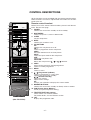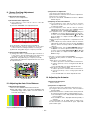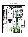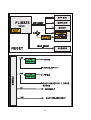
1
website:http://biz.LGservice.com
e-mail:http://www.LGEservice.com/techsup.html
DLP Projection TV
SERVICE MANUAL
CHASSIS : MB-05DA
MODEL : 44/52SZ8R
MODEL : 44/52SZ8R-ZA
CAUTION
BEFORE SERVICING THE CHASSIS,
READ THE SAFETY PRECAUTIONS IN THIS MANUAL.
TV/AV
MENU
OK
VOL
PR
CONTENTS
CONTENTS ..................................................................................................................... 2
SAFETY PRECAUTIONS ................................................................................................3
SERVICING PRECAUTIONS .......................................................................................... 4
CONTROL DESCRIPTIONS ............................................................................................6
SPECIFICATIONS ..........................................................................................................10
ADJUSTMENT INSTRUCTIONS ....................................................................................18
BLOCK DIAGRAM..........................................................................................................26
EXPLODED VIEW .................................................................................................... 32,34
EXPLODED VIEW PARTS LIST ................................................................................33,35
REPLACEMENT PARTS LIST .......................................................................................36
REPLACEMENT THE LAMP .........................................................................................46
SVC. SHEET ......................................................................................................................
PRINTED CIRCUIT BOARD ...............................................................................................
- 2 -
SAFETY PRECAUTIONS
IMPORTANT SAFETY NOTICE
Many electrical and mechanical parts in this chassis have special safety-related characteristics. These parts are identified by
in
the Schematic Diagram and Replacement Parts List.
It is essential that these special safety parts should be replaced with the same components as recommended in this manual to
prevent X-RADIATION, Shock, Fire, or other Hazards.
Do not modify the original design without permission of manufacturer.
Leakage Current Cold Check(Antenna Cold Check)
General Guidance
An isolation Transformer should always be used during
the servicing of a receiver whose chassis is not isolated from
the AC power line. Use a transformer of adequate power rating
as this protects the technician from accidents resulting in
personal injury from electrical shocks.
It will also protect the receiver and it's components from being
damaged by accidental shorts of the circuitry that may be
inadvertently introduced during the service operation.
If any fuse (or Fusible Resistor) in this TV receiver is blown,
replace it with the specified.
With the instrument AC plug removed from AC source,
connect an electrical jumper across the two AC plug prongs.
Place the AC switch in the on position, connect one lead of
ohm-meter to the AC plug prongs tied together and touch other
ohm-meter lead in turn to each exposed metallic parts such as
antenna terminals, phone jacks, etc.
If the exposed metallic part has a return path to the chassis, the
measured resistance should be between 1MΩ and 5.2MΩ.
When the exposed metal has no return path to the chassis the
reading must be infinite.
An other abnormality exists that must be corrected before the
receiver is returned to the customer.
Leakage Current Hot Check (See below Figure)
When replacing a high wattage resistor (Oxide Metal Film
Resistor, over 1W), keep the resistor 10mm away from PCB.
Keep wires away from high voltage or high temperature parts.
Due to high vacuum and large surface area of picture tube,
extreme care should be used in handling the Picture Tube.
Do not lift the Picture tube by it's Neck.
Before returning the receiver to the customer,
always perform an AC leakage current check on the exposed
metallic parts of the cabinet, such as antennas, terminals, etc.,
to be sure the set is safe to operate without damage of
electrical shock.
Plug the AC cord directly into the AC outlet.
Do not use a line Isolation Transformer during this check.
Connect 1.5K/10watt resistor in parallel with a 0.15uF capacitor
between a known good earth ground (Water Pipe, Conduit, etc.)
and the exposed metallic parts.
Measure the AC voltage across the resistor using AC
voltmeter with 1000 ohms/volt or more sensitivity.
Reverse plug the AC cord into the AC outlet and repeat AC
voltage measurements for each exposed metallic part. Any
voltage measured must not exceed 0.75 volt RMS which is
corresponds to 0.5mA.
In case any measurement is out of the limits specified, there is
possibility of shock hazard and the set must be checked and
repaired before it is returned to the customer.
Leakage Current Hot Check circuit
AC Volt-meter
To Instrument's
exposed
METALLIC PARTS
0.15uF
1.5 Kohm/10W
- 3 -
Good Earth Ground
such as WATER PIPE,
CONDUIT etc.
SERVICING PRECAUTIONS
CAUTION: Before servicing receivers covered by this service
manual and its supplements and addenda, read and follow the
SAFETY PRECAUTIONS on page 3 of this publication.
NOTE: If unforeseen circumstances create conflict between the
following servicing precautions and any of the safety
precautions on page 3 of this publication, always follow the
safety precautions. Remember: Safety First.
General Servicing Precautions
1. Always unplug the receiver AC power cord from the AC
power source before;
a. Removing or reinstalling any component, circuit board
module or any other receiver assembly.
b. Disconnecting or reconnecting any receiver electrical plug
or other electrical connection.
c. Connecting a test substitute in parallel with an electrolytic
capacitor in the receiver.
CAUTION: A wrong part substitution or incorrect
polarity installation of electrolytic capacitors may result
in an explosion hazard.
d. Discharging the picture tube anode.
2. Test high voltage only by measuring it with an appropriate
high voltage meter or other voltage measuring device (DVM,
FETVOM, etc) equipped with a suitable high voltage probe.
Do not test high voltage by "drawing an arc".
3. Discharge the picture tube anode only by (a) first connecting
one end of an insulated clip lead to the degaussing or kind
aquadag grounding system shield at the point where the
picture tube socket ground lead is connected, and then (b)
touch the other end of the insulated clip lead to the picture
tube anode button, using an insulating handle to avoid
personal contact with high voltage.
4. Do not spray chemicals on or near this receiver or any of its
assemblies.
5. Unless specified otherwise in this service manual, clean
electrical contacts only by applying the following mixture to
the contacts with a pipe cleaner, cotton-tipped stick or
comparable nonabrasive applicator; 10% (by volume)
Acetone and 90% (by volume) isopropyl alcohol (90%-99%
strength)
CAUTION: This is a flammable mixture.
Unless specified otherwise in this service manual, lubrication
of contacts in not required.
6. Do not defeat any plug/socket B+ voltage interlocks with
which receivers covered by this service manual might be
equipped.
7. Do not apply AC power to this instrument and/or any of its
electrical assemblies unless all solid-state device heat sinks
are correctly installed.
8. Always connect the test receiver ground lead to the
receiver chassis ground before connecting the test receiver
positive lead.
Always remove the test receiver ground lead last.
9. Use with this receiver only the test fixtures specified in this
service manual.
CAUTION: Do not connect the test fixture ground strap to
any heatsink in this receiver.
Electrostatically Sensitive (ES) Devices
Some semiconductor (solid state) devices can be damaged
easily by static electricity. Such components commonly are
called Electrostatically Sensitive (ES) Devices. Examples of
typical ES devices are integrated circuits and some field effect
transistors and semiconductor "chip" components. The
following techniques should be used to help reduce the
incidence of component damage caused by static by static
electricity.
1. Immediately before handling any semiconductor component
or semiconductor-equipped assembly, drain off any
electrostatic charge on your body by touching a known earth
ground. Alternatively, obtain and wear a commercially
available discharging wrist strap device, which should be
removed to prevent potential shock reasons prior to
applying power to the unit under test.
2. After removing an electrical assembly equipped with ES
devices, place the assembly on a conductive surface such as
aluminum foil, to prevent electrostatic charge buildup or
exposure of the assembly.
3. Use only a grounded-tip soldering iron to solder or unsolder
ES devices.
4. Use only an anti-static type solder removal device. Some
solder removal devices not classified as "anti-static" can
generate electrical charges sufficient to damage ES devices.
5. Do not use freon-propelled chemicals. These can generate
electrical charges sufficient to damage ES devices.
6. Do not remove a replacement ES device from its protective
package until immediately before you are ready to install it.
(Most replacement ES devices are packaged with leads
electrically shorted together by conductive foam, aluminum
foil or comparable conductive material).
7. Immediately before removing the protective material from
the ieads of a replacement ES device, touch the protective
material to the chassis or circuit assembly into which the
device will be installed.
CAUTION:Be sure no power is applied to the chassis or
circuit, and observe all other safety precautions.
8. Minimize bodily motions when handling unpackaged
replacement ES devices. (Otherwise harmless motion such
as the brushing together of your clothes fabric or the lifting
of your foot from a carpeted floor can generate static
electricity sufficient to damage an ES device.)
General Soldering Guidelines
1. Use a grounded-tip, low-wattage soldering iron and
appropriate tip size and shape that will maintain tip
temperature within the range or 500°F to 600°
F.
2. Use an appropriate gauge of RMA resin-core solder
composed of 60 parts tin/40 parts lead.
3. Keep the soldering iron tip clean and well tinned.
4. Thorohly clean the surfaces to be soldered. Use a mall wire
bristle (0.5 inch, or 1.25cm) brush with a metal handle.
Do not use freon-propelled spray-on cleaners.
5. Use the following unsoldering technique
a. Allow the soldering iron tip to reach normal temperature.
(500°
F to 600°
F)
b. Heat the component lead until the solder melts.
c. Quickly draw the melted solder with an anti-static,
suction-type solder removal device or with solder braid.
CAUTION: Work quickly to avoid overheating the circuit
board printed foil.
6. Use the following soldering technique.
a. Allow the soldering iron tip to reach a normal
temperature (500°
F to 600°
F)
b. First, hold the soldering iron tip and solder the strand
against the component lead until the solder melts.
- 4 -
c. Quickly move the soldering iron tip to the junction of the
component lead and the printed circuit foil, and hold it
there only until the solder flows onto and around both the
component lead and the foil.
CAUTION: Work quickly to avoid overheating the circuit
board printed foil.
d. Closely inspect the solder area and remove any excess
or splashed solder with a small wire-bristle brush.
IC Remove/Replacement
Some chassis circuit boards have slotted holes (oblong) through
which the IC leads are inserted and then bent flat against the
circuit foil. When holes are the slotted type, the following
technique should be used to remove and replace the IC. When
working with boards using the familiar round hole, use the
standard technique as outlined in paragraphs 5 and 6 above.
Removal
1. Desolder and straighten each IC lead in one operation by
gently prying up on the lead with the soldering iron tip as the
solder melts.
2. Draw away the melted solder with an anti-static suctiontype solder removal device (or with solder braid) before
removing the IC.
Replacement
1. Carefully insert the replacement IC in the circuit board.
2. Carefully bend each IC lead against the circuit foil pad and
solder it.
3. Clean the soldered areas with a small wire-bristle brush.
(It is not necessary to reapply acrylic coating to the areas).
"Small-Signal" Discrete Transistor
Removal/Replacement
1. Remove the defective transistor by clipping its leads as
close as possible to the component body.
2. Bend into a "U" shape the end of each of three leads
remaining on the circuit board.
3. Bend into a "U" shape the replacement transistor leads.
4. Connect the replacement transistor leads to the
corresponding leads extending from the circuit board and
crimp the "U" with long nose pliers to insure metal to metal
contact then solder each connection.
Power Output, Transistor Device
Removal/Replacement
1. Heat and remove all solder from around the transistor leads.
2. Remove the heatsink mounting screw (if so equipped).
3. Carefully remove the transistor from the heat sink of the
circuit board.
4. Insert new transistor in the circuit board.
5. Solder each transistor lead, and clip off excess lead.
6. Replace heatsink.
Diode Removal/Replacement
1. Remove defective diode by clipping its leads as close as
possible to diode body.
2. Bend the two remaining leads perpendicular y to the circuit
board.
3. Observing diode polarity, wrap each lead of the new diode
around the corresponding lead on the circuit board.
4. Securely crimp each connection and solder it.
5. Inspect (on the circuit board copper side) the solder joints of
the two "original" leads. If they are not shiny, reheat them
and if necessary, apply additional solder.
Fuse and Conventional Resistor
Removal/Replacement
1. Clip each fuse or resistor lead at top of the circuit board
hollow stake.
2. Securely crimp the leads of replacement component around
notch at stake top.
3. Solder the connections.
CAUTION: Maintain original spacing between the replaced
component and adjacent components and the circuit board
to prevent excessive component temperatures.
Circuit Board Foil Repair
Excessive heat applied to the copper foil of any printed circuit
board will weaken the adhesive that bonds the foil to the circuit
board causing the foil to separate from or "lift-off" the board.
The following guidelines and procedures should be followed
whenever this condition is encountered.
At IC Connections
To repair a defective copper pattern at IC connections use the
following procedure to install a jumper wire on the copper
pattern side of the circuit board. (Use this technique only on IC
connections).
1. Carefully remove the damaged copper pattern with a sharp
knife. (Remove only as much copper as absolutely
necessary).
2. carefully scratch away the solder resist and acrylic coating
(if used) from the end of the remaining copper pattern.
3. Bend a small "U" in one end of a small gauge jumper wire and
carefully crimp it around the IC pin. Solder the IC connection.
4. Route the jumper wire along the path of the out-away
copper pattern and let it overlap the previously scraped end
of the good copper pattern. Solder the overlapped area and
clip off any excess jumper wire.
At Other Connections
Use the following technique to repair the defective copper
pattern at connections other than IC Pins. This technique
involves the installation of a jumper wire on the component
side of the circuit board.
1. Remove the defective copper pattern with a sharp knife.
Remove at least 1/4 inch of copper, to ensure that a
hazardous condition will not exist if the jumper wire opens.
2. Trace along the copper pattern from both sides of the
pattern break and locate the nearest component that is
directly connected to the affected copper pattern.
3. Connect insulated 20-gauge jumper wire from the lead of
the nearest component on one side of the pattern break to
the lead of the nearest component on the other side.
Carefully crimp and solder the connections.
CAUTION: Be sure the insulated jumper wire is dressed so
the it does not touch components or sharp edges.
- 5 -
CONTROL DESCRIPTIONS
All the functions can be controlled with the remote control handset.
Some functions can also be adjusted with the buttons on the front
panel of the set.
Remote control handset
POWER
Before you use the remote control handset, please install the batteries. See the next page.
1
2
3
4
MULTIMEDIA
TV/AV
MUTE
SLEEP
PIP
TEXT
5
PR -
6
7
13
2. MULTIMEDIA
selects Component 1/2, RGB or HDMI modes.
PR +
SWAP
MENU
VOL
3. SLEEP
sets the sleep timer.
INPUT
PR
CANCEL/EXIT
OK
15 4. MUTE
switches the sound on or off.
5. PIP BUTTONS
PIP
switches the sub picture on or off.
PR +/selects a programme for the sub picture.
SWAP
alternates between main and sub picture.
INPUT
selects the input mode for the sub picture.
SIZE
adjusts the sub picture size.
POSITION
VOL
8
PR
1
2
3
4
5
6
7
8
9
PSM
0
SSM
POSITION
SIZE
STILL
INDEX
TIME
REVEAL
MIX
MODE
1. POWER
switches the set on from standby or off to standby.
Moves the sub picture to
9
10
11
12
18
I/II
STOP
REW
M
/
PLAY
8.
14
REC
FF
/ E or F / G direction.
6. SWAP
returns to the previously viewed programme.
16
selects a favorite programme.
17 7. MENU
selects a menu.
L IS T
ARC
P/STILL
?
D
19
/ E (Programme Up/Down)
selects a programme or a menu item.
switches the set on from standby.
F / G (Volume Down/Up)
adjusts the volume.
adjusts menu settings.
OK
accepts your selection or displays the current mode.
D
9. NUMBER BUTTONS
switches the set on from standby or directly select a number.
10. PSM (Picture Status Memory)
recalls your preferred picture setting.
11. TELETEXT BUTTONS (option)
These buttons are used for teletext.
For further details, see the ‘Teletext’ section.
(With TELETEXT)
12. LIST
displays the programme table.
- 6 -
13. TV/AV
selects the remote operating mode.
switches the set on from standby.
POWER
14. ARC (Aspect Ratio Control)
changes the picture format.
1
2
MULTIMEDIA
TV/AV
LIST
ARC
MUTE
PIP
15. CANCEL/EXIT
Clears all on-screen displays and returns to TV viewing from any 12
menu.
4
6
17. STILL
freezes motion of the picture.
7
18. I/II
selects the language during dual language broadcast.
selects the sound output.
8
14
5
PR -
16. SSM (Sound Status Memory)
recalls your preferred sound setting.
13
PR +
SWAP
MENU
VOL
INPUT
PR
OK
CANCEL/EXIT
15
VOL
19. VCR BUTTONS
control a video cassette recorder.
PR
Note : In teletext mode, the PR + / -, SWAP and INPUT buttons are
used for teletext function.
9
Battery installation
The remote control handset is powered by two AAA type batteries.
To load the batteries, turn the remote control handset over and 10
open the battery compartment. Install two batteries as indicated by
the polarity symbols ( + and - ) marked inside the compartment.
1
2
3
4
5
6
7
8
9
PSM
0
SSM
POSITION
SIZE
STILL
SLEEP
I/II
REW
P/STILL
PLAY
REC
FF
Note : To avoid damage from possible battery leakage, remove the
batteries if you do not plan to use the remote control handset for an
extended period of time.
(Without TELETEXT)
- 7 -
17
18
3
STOP
16
19
Front panel
Lamp indicator, operation indicator, and temperature indicator, located side the front panel controls
reveal the operating status of the DLP(Digital Light Processing) projection TV.
ON/OFF
TV/AV
1
MENU
OK
VOL
PR
TV/AV
MENU
OK
VOL
PR
2
3
4
5
6
7
8
9
10
1. REMOTE CONTROL SENSOR
7. OPERATION INDICATOR (Refer to p.7)
2. TV/AV
selects the remote operating mode.
switches the set on from standby.
8. LAMP INDICATOR (Refer to p.7)
3. MENU
selects a menu.
10. MAIN POWER (ON/OFF)
switches the set on or off.
4. OK
accepts your selection or displays the current
mode.
Note : There might be a faint white trace on the
center of the screen according to the position.
This is normal and is a characteristic of the
screen.
5.
F / G (Volume Down/Up)
adjusts the volume.
adjusts menu settings.
6.
D / E (Programme Up/Down)
selects a programme or a menu item.
switches the set on from standby.
9. TEMPERATURE INDICATOR (Refer to p.7)
- 8 -
Rear panel
(R)
AUDIO
AV4 INPUT
SOCKET
(L)/
MONO
VIDEO
S-VIDEO
COMPONENT
INPUT 2
INPUT 1
480i/480p/
576i/576p/
720p/1080i
480i/480p/
576i/576p/
720p/1080i
(R)
AUDIO
VIDEO
AV1
AV2
AV3
PC/DTV
(SXGA/
480p/
576p/
720p/
1080i)
(L)/
MONO
Y
S-VIDEO
PB
PR
U
P P
GO
R R
A T
D
E
RGB INPUT
S-VIDEO
INPUT
SOCKET
AV3
INPUT
(L)
(L)
AUDIO
AUDIO
(R)
(R)
AV 4
INPUT
DVI / RGB INPUT
HDMI/DVI INPUT
UPGRADE PORT
This port is used to
upgrade the software version and debug without
changing the hardware.
Be careful not to use this
port. Just contact your
dealer or service centre.
COMPONENT
AV1
AV2
AV1/AV2/AV3 INPUT
SOCKETS
AV3
PC/DTV
(XGA/
480p/
576p/
720p/
1080i)
INPUT 2
INPUT 1
480i/480p/
576i/576p/
720p/1080i
480i/480p/
576i/576p/
720p/1080i
Y
PB
PR
U
P P
GO
R R
A T
D
E
RGB INPUT
DTV/DVD
INPUT
(L)
AUDIO
(R)
(L)
AUDIO
(R)
DVI / RGB INPUT
HDMI/DVI
AERIAL
SOCKET
RGB INPUT
HDMI/DVI
•Status Indicators
Operation Indicator
Off
Red
Green
Orange (flashing)
Orange
Red (flashing)
Lamp Indicator
Red
Green (flashing)
Red
Temperature Indicator
Red (flashing)
Orange
Power cord is not connected or power switch is off
Power Cord is connected, unit is on standby.
On
Preparing operation in standby.
Projection lamp is reaching the end of its life and
needs to be replaced with a new lamp.
There is a problem with the lamp or around it.
Contact an authorized service center.
Lamp life over.
The lamp cover is not closed.
The set has shut down due to overheating.
After viewing the phrase “Thermal High Error”
The set has shut down, check the cooling fan.
Thermal warning.
- 9 -
SPECIFICATIONS
NOTE : Specifications and others are subject to change without notice for improvement.
V
Application Range
This spec sheet is applied to the 44/52” DLP TV used MB-05DA chassis.
Chassis
Model Name
Market Place
Brand
MB-05DA
44/52SZ8R-ZA
United Kingdom
LG
Remark
(RZ-44/52SZ84DB)
V
Specification
Each part is tested as below without special appointment.
1) Temperature : 25!5°C (CST : 40°C! 2°C)
2) Relative Humidity : 65!10%
3) Power Voltage : Standard input voltage(AC 230V!10%, 50Hz)
* Standard Voltage of each products is marked by model.
4) Specification and performance of each parts are followed each drawing and specification by part number in accordance with BOM.
5) The receiver must be operated for about 20 minutes prior to the adjustment.
V
Test Method
1) performance : LGE TV test method followed.
2) Demanded other specification.
Safety : CB specification
EMC : CE specification
Model Name
Market
Remark
Appliance
44/52SZ8R-ZA
United Kingdom
Safety : EN55013, EMI : EN55020
TEST
RZ-44/52SZ84DB
- 10 -
V
General Specification
No
1
Aspect Ratio
16:9(wide)
2
Operating Environment
1) Temp
: 0~40 deg
2) Humidity
: 0~85%
3) Temp
: -20~60 deg
4) Humidity
: 0~85%
3
4
V
Specification
Item
Storage Environment
Input Voltage
Remark
LGE SPEC
AC 230V, 50Hz
Model Specification
No
Specification
Item
1
Market
EU
2
Broadcasting system
RF
Remark
PAL/ SECAM - B/ G
PAL/ SECAM - D/ K
Except PAL-M/N
PAL - I/ I
AV
PAL/ SECAM
NTSC - 3.58/ 4.43
3
Available Channel
BAND
PAL
VHF
E02~E12
UHF
E21~E69
CATV
S01~ S20
HYPER
S21~S41
4
Receiving system
Upper Heterodyne
5
AV Input(4EA)
PAL, SECAM, NTSC
SCART1(Full) : AV1, TV out
SCART2(Half) : AV2, Monitor out
SCART3(Half) : AV3
Side AV
: AV4, S-Video1
6
Monitor Out(1EA)
PAL, SECAM, NTSC
7
S-Video Input(1EA)
PAL, SECAM, NTSC
8
Component Input(2EA)
Y/ Pb / Pr
9
RGB Input
RGB-PC/ DTV
10
HDMI Input
HDMI-PC/ DTV
11
Audio Input(4EA)
PC Audio (1EA), Component (2EA), AV (1EA)
12
Wired Control
Discrete IR
S-Video 1 first
D-sub 15 pin
L/ R Input
- 11 -
V
Feature and Function
No
1
Specification
Item
44/52SZ
RF Input
1
2 Tuner (PAL-BG/ I/ DK,
8R-ZA
Remark
Rear
SECAM-BG/ DK)
AV Input
4
CVBS/ L/ R / S-VHS(S-VHS Priority)
Rear 3 Side 1
Monitor Out
1
CVBS/ L / R
Rear
Component Input
2
480i/ 576i/ 480p/ 576p/ 720p/ 1080i
Rear
RGB Input
1
RGB-PC : Up to XGA 85Hz
Rear
RGB-DTV : 480p/ 576p/ 720p/ 1080i
HDMI Input
1
HDMI-TV : Up to XGA 85Hz
Rear
HDMI-DTV : 480p/ 576p/ 720p/ 1080i
RS-232C
1
Remote Control, S/W Download
Rear
IR Input
1
Discrete IR
Rear
2
Remocon Code
NEC Code
3
Remote control
Wireless Remote Control
4
Local Key
TV / AV, MENU, OK, FVOLG, DPRE
5
Menu
Auto programme
(Channel
(Auto program)
/ Station)
Manual programme
Storage, System, Band, Channel, Fine, Search,
(Manual program)
Name, Booster
Programme edit
Del, Copy, Move, Skip
System, Storage(0~99), Start
(Program edit)
Favorite programme
8 Channel
(Favorite program)
6
7
Menu
PSM(Picture Status Mode) Dynamic, Standard, Mild, User
(Picture)
CSM(Color Status Mode)
Cool, Normal, Warm, User( Red, Green, Blue )
XD
On / Off
ACM
Freshtone, Greentone, Bluetone
SRGB
On / Off
User
Contrast, Brightness, Colour, Sharpness, Tint
SSM(Sound Status Mode)
SRS TSXT, Flat, Music, Movie, Speech
Menu
User
(Sound)
BBE
On / Off
AVL(Auto Volume Limit)
On / Off
Balance, Treble, Bass
Balance
8
9
Equalizer
120/ 200/ 500/ 1.2K/ 3K/ 7.5K/ 12KHz
Menu
Clock
User Setting
(Time)
Off Time
On / Off ( Time : User Setting)
On Time
On / Off ( Time/ Volume/ Programme :User Setting )
Auto Sleep
On / Off
Menu
Child lock(Key lock)
On / Off
(Special)
XD Demo
On : Left arrow(Vol+) Key
Menu
Auto config
RGB PC
(Screen)
ARC
RF/ AV/ Component 480i/ 480p/ 576i/ 576p
Off : Exit Key
10
Auto Position and Auto Clock&Phase
: Spectacle, Full, Original, 4:3, 16:9, 14:9, Zoom
Component-DTV/ RGB-DTV : 4:3, 16:9, Zoom
RGB-PC/ HDMI : 4:3, 16:9
- 12 -
No
10
Item
Menu
Specification
Manual config
(Screen)
Available for only RGB PC
Phase : 0 ~ 63
Clock : -127 ~ +128
Cinema (Film Mode)
On/ Off
RF, AV1/2, Component 480i,576i
NR
3D NR : 0~ 2
Except RGB-PC / HDMI-PC
(Luma Noise Reduction)
MPEG NR : 0~15
Initialize user data
Reset
11
Menu
Remark
TV-> AV1-> AV2->SAV2-> AV3->AV4->
Input(Main)
(PIP/DW)
COMPONENT1->COMPONENT2-> RGB->
HDMI/ DVI
12
DW
DW1, DW2, OFF
PIP
On/ Off
PIP Input(Sub Input)
Main Input
Sub Input
All Input
All (Except Main Input)
Win. Size
Variable(1/16~ 1/4 of Display size)
PIP Mode Only
Win. Position
Variable
PIP Mode Only
PIP transparency
0~10
PIP Mode Only
PIP System
Auto/ PAL/ SECAM/ NTSC
Hot Key
Input
(Remote) Select
Mute-media
TV/ AV
(TV/ Video)
COMPONENT1->COMPONENT2->RGB->HDMI
TV-> AV1-> AV2-> SAV2->AV3->AV4->
COMPONENT1->COMPONENT2-> RGB->
HDMI/ DVI
PIP/ DW
PIP-> DW1-> DW2-> Off
ZOOM+/ ZOOM-
100~ 300%
MUTE
Audio Mute
Text
SLEEP
Sleep Time 10~ 240 Min
LIST
Channel List
I/ II(RZ/ RT)
SIF Control
SWAP
O
Text mode : Yellow Key
Favorite : Favorite
Favorite off : Q.view
Pip/ Twin : Main/ Sub Swap
PIP INPUT
TV-> AV1-> AV2-> SAV2-> AV3->AV4->
COMPONENT1-> COMPONENT2-> RGB->
HDMI/ DVI
SSM
SRS TSXT->Flat->Music->Movie->Speech->User
PSM
Dynamic-> Standard-> Mild-> User
FAVORITE
SIZE
POSITION
HOLD
TIME
ETC.
POWER, Numeric(0~9), PR+/-, ARC, PRD,E,
VOLF,G,Mute,PIP Input, PIP PRD,E
13
Adaptive
3D Comb Filter
O
DCDI(MADI)
O
Motion Detection
O
Noise Reduction
O
- 13 -
V
Power
No
Specification
Item
Remark
Min
V
Typ
Max
Unit
1
Power ON/OFF operation
2
Staring Voltage
-20
20
%
Normal 220V
3
Staring Voltage, -10 Degree
-15
15
%
Normal 220V
4
DC Voltage, Ballast
370
390
410
V
5
DC Voltage, 5V-STBY
4.5
5
5.5
V
6
DC Voltage, 3.3V-STBY
3.135
3.3
3.465
V
7
DC Voltage, 2.5V-STBY
2.375
2.5
2.625
V
8
DC Voltage, 1.8V-STBY
1.71
1.8
1.89
V
9
DC Voltage,Tuning Voltage
29
31
33
V
10
DC Voltage, DLP Driver, 3.5V
3.135
3.3
3.465
V
11
DC Voltage, DLP Driver, 2.5V
2.375
2.5
2.625
V
12
DC Voltage, DLP Driver, 5V
4.5
5
5.5
V
13
DC Voltage, DLP Driver, 12V
11.4
12
12.6
V
14
DC Voltage,Fan
5.7
5.9
6.15
V
15
Audio Amp
24
26
28
V
10000
times
External Interface
Specification
No
Remark
Item
Min
Typ
Max
Unit
1
1.1
Vpp
1
Video Input Level
0.9
2
Video Input Frequency Response
3.0
MHz
At AV output
3
Video output S/N
40
dB
At AV output
4
S-Video Input Level (Y)
0.85
5
S-Video Input Level (C-Burst)
0.143
6
Component Video Input Level
0.6
1.15
Vpp
0.286
Vpp
0.7
0.8
Vpp
0.7
0.8
Vpp
1
(Y, CB / PB, CR / PR)
7
R/G/B Video Input Level
0.6
8
Audio Input S/N
40
9
Audio Input Distortion
10
Audio Input Level
11
Audio Output Level
12
Audio Input Frequency Range
2
%
0.3
0.4
0.5
Vrms
NTSC
0.4
0.5
0.6
Vrms
PAL, SECAM
0.4
0.5
0.6
Vrms
0.05
kHz
Low
High
dB
7
- 14 -
V
Component Video Input (Y, PB, PR)
Specification
Proposed
No
Resolution
V
H-freq(kHz)
V-freq(Hz)
Pixel clock
1
720*480
15.73
59.94
13.500
SDTV, DVD 480I(525I)
2
720*480
15.75
60.00
13.514
SDTV, DVD 480I(525I)
3
720x576
15.625
50.00
13.500
SDTV, DVD 576I(625I)
4
720*480
31.47
59.94
27.000
SDTV 480P
5
720*480
31.50
60.00
27.027
SDTV 480P
6
720x576
31.25
50.00
27.000
SDTV 576P
7
1280x720
44.96
59.94
74.176
HDTV 720P
8
1280x720
45.00
60.00
74.250
HDTV 720P
9
1280*720
37.50
50.00
74.250
HDTV 720P 50Hz
10
1920x1080
33.72
59.94
74.176
HDTV 1080I
11
1920x1080
33.75
60.00
74.250
HDTV 1080I
12
1920*1080
28.125
50.00
74.250
HDTV 1080I 50Hz
HDMI Input(DTV)
Specification
Proposed
No
Resolution
H-freq(kHz)
V-freq(Hz)
Pixel clock
1
720*480
31.47
59.94
27.000
SDTV 480P
2
720*480
31.50
60.00
27.027
SDTV 480P
3
720x576
31.25
50.00
27.000
SDTV 576P
4
1280x720
44.96
59.94
74.176
HDTV 720P
5
1280x720
45.00
60.00
74.250
HDTV 720P
6
1280x720
37.50
50.00
74.250
HDTV 720P 50Hz
7
1920*1080
33.72
59.94
74.176
HDTV 1080I
8
1920*1080
33.75
60.00
74.250
HDTV 1080I
9
1920*1080
28.125
50.00
74.250
HDTV 1080I 50Hz
- 15 -
V
Option
No
Item
Specification
1
Area Code
4
2
OPTION1
200PR
Description
0 : 100 PR Memory
1 : 200PR Memory
(Tuner opt)
ACMS
0 : CH Memory On
1 : CH Memory Off
TEXT
TOP : A patent right payment nation
FLOP : Basic
Off : Text Off
CH+AU
0 : Others
1 : China/ Australia Frequency Table
BOOTS
AGC-Reference
3
OPTION2
SYS
(Audio opt)
Booster On/ Off control for 2 Tuner sys
AGC Threshold point
BGIDKM : NTSC for N-EU
BGIDKL : Secam for EU
A2 ST
0 : Acting FM-ST after checking Nicam
1 : Acting Nicam & FM-ST
I II SAVE
0 : Acting FM-ST after checking Nicam
1 : Acting Nicam & FM-ST
HDEV
0 : Off
1 : Audio High deviation on after checking over-Mod
V-Curve0
0 : Slow LGE Vo.1 Curve
1 : Fast Vol Curve
MONO
0 : ACting followed SIF & I/ II
1 : Always Meno 1 : TTX
Audio Delay
4
OPTION3
Scart
(Board opt)
5
0~150
0 : Phone Jack
1 : Scart Jack
OPTION4
Default Lang
(Lang opt)
LANG
English, France, German, Spanish, Italian, Chinese, Russian
EU5 : Default Lang. 5
Non-EU7 : Default Lang. 7
T LANG
0 : West Europe
1 : East EU1
2 : Turkey
3 : East-EU2(Czecho/ Hungary)
4 : Cyrillic1
5 : Cyrillic2
6 : Cyrillic3
- 16 -
Remark
No
Item
Specification
Remark
Description
7 : Turkey/ Greek1
8 : Turkey/ Greek2
9 : Turkey/ Greek3
10 : Arabic/ French
11 : Arabic/ English
12 : Arabic/ Hebrew1
13 : Arabic/ Hebrew2
14 : Farsi/ English
15 : Farsi/ French
16 : Farsi All
6
OPTION5
INDEX
(ETC opt)
0 : Index Off
1 : Index On
Navigation Key
On : Only work Navigation Key
Off : Work both Navigation and Vol/ CH Key
Favorite Key
On : Only work Favorite Key
Off : Work both Favorite and Pip Swap Key
V
Lamp & Temp
IN-START for adjustment Remote Controller -> Lamp & Temp
No.
Item
Market Place
Remark
1
Lamp Life Time[khr]
The length of time that lamp is alive to capacity
2
Lamp use Time[hr]
The length of time that lamp is used up to now
3
Lamp Current Temp
4
Lamp Warn Temp
Warm below Warn Temp
5
Lamp Error Temp
Power off below Warn Temp
6
Off-On Waiting[sec]
Waiting time when reoperation
For Engineering
Not real Temp
- 17 -
ADJUSTMENT INSTRUCTIONS
1. Application Object
4. Adjustment the optical engine
This instruction is for the application to the DLP Projection
2. Notes
1) The power source insulation of this DLP Projection is
not charging type and you may not use the
transformer for insulation. But you’d better adjust the
set after operating it with insulation transformer
between power supply cable and input part of the set
for protecting the adjusting equipment.
2) The adjustment must be performed under the correct
sequence.
3) The adjustment must be performed in the circumstance
of 25 ! 5°C of temperature and 65 ! 10% of relative
humidity if there is no specific designation.
4) The input voltage of the receiver must keep 220V, 60Hz
in adjusting.
5) The set must be operated for 5 minutes preliminary
before adjustment if there is no specific designation.
The preliminary operation must be performed after
receiving 100% white pattern,but reception of the
moving picture may also be possible in unavoidable
case.
3. Composition of Adjustment Mode
1) All adjustment mode by pressing down ADJ key of a
adjustment remote controller, after adjustment as they
also come out by pressing down ADJ key.
2) Adjustment mode component : When early ADJ
presses presented screen component.
A
B
<Fig 2>
1) After placing the optical engine on the JIG, adjust
illuminator by adjusting with automatic adjustment the
B as shown <Fig 2>.
(1) When adjust illuminator, search the scope does not fall
in illuminator and Tilt adjustment complete with
automation equipment in that scope.
(2) After adjusting, A fix with Screw using automation
equipment.
2) In order to move the Optical system adjusted the Tilt to
center of the screen, adjust with automatic device.
After automatically adjusting the illuminator in <Fig 3>
adjust the position. ( Refer to Automatic Adjustment
Sequence )
A
<Fig 3>
Start
DMD/Lens Chucking
Screw Fwd/Bwd
Check Focus
DMD Adjustment(Tilt, Illuminator)
Check DMD
DMD Manual
NG
Lens Adjustment(X & Y)
Check Lens
Manual
NG
<Fig 1.Adjustment Mode OSD>
Lens Screw Fix.
Check Lens
Restart
3) Select menu to adjust with using (CH+(D), CH-(E)) key
above screen and press Enter key <Fig 1>.
4) After entering into ADJ Mode list, using CH+(D), CH-(E)
key, after choosing an adjustment list one more time,
adjustment value is changed by using ENTER Key.
5) Press the ADJ key to come out after adjustment.
6) Preparation for Adjustment
(1) Connect the power to TV Set and set the status of
“Power on”.
(2) Heat-Run must operate over 5 minute before
adjustment.
- 18 -
Lens Chuck Open
DMD Adjustment(X & Y & Tilt)
Check DMD
DMD Manual
NG
DMD Screw Fix.
Check DMD
Restart
DMD Chuck Back
End
<Reference> Automatic Adjustment Sequence
7. Caution for DMD(Digital Micro-mirror
Device)
A. Inject the resilock
1) Caution for DMD ESD
(1) You connect the grounding to prevent ESD (Electrostatic
Discharge) when handing the DMD.
(2) The worker have to wear wrist strap that connect to ground.
(3) Electric workshop and an electric conductor surface
connect to ground.
(4) Save the DMD after removement a static electricity.
Keep it at an exclusive case when moving it. When
grounding, open the case.
(5) Put on gloves that to prevent static electricity. If it’s old,
replace it.
(6) The work is done at the electro static-free location. Attach the
tape or remove dust on the front or back pin of DMD glass.
B. Ancor Screw
<Fig 4>
3) After adjusting the illuminator, adjust the focus by
using the focus adjustment screw of projection lens.
After adjusting, fasten the screw tightly and secure
with sealer <Fig 4>.
* Note: The focus check point is not the screen center but the
upper/ lower screen.
* The pattern When Focus adjustment
2) Caution
(1) Keep the procedure and caution to prevent the screen
strange phenomenon. Don’t make a scratch.
(2) When DMD stains with dust, polish the front and back DMD
with soft wiper. Then, polish the front and back DMD after
rotating 180 degree the DMD. If necessary, take a inspection.
(3) Don’t clean the DMD with the high pressure. Because
the electric static and pollution influence to DMD.
* TI Reference : DMD Handling Specification, DMD Cleaning.
<Fig 5>
1) Come to Cross Hatch in the adjustment T/X Adj>Pattern.
2) Adjustment to the most adequate Focus being changed
Focus adjustment Knob.
3) Adjustment /Check for Focus of mark part to be same.
a. Focus : Center Best
b. Flare : 1.5pixel
4) After finishing adjustment, adjustment Knob is made to be Fix.
8. EDID Data Input
5. Check the CWI/ NDC adjustment
movement and Default data
(Base value --> CWI: 160, NDC: 12)
1) Required Test Equipment
: Remote control
1) Required Test Equipment
(1) PC, S/W for writing DDC(S/W : EDID TESTER Ver. 2.5)
(2) A JIG for adjusting.
(3) Serial(9Pin or USB) to D-sub 15Pin cable, D-sub 15 Pin
cable. DVI to HDMI cable
2) Preparation for Adjustment & Setting of Device
(1) Set devices as above Fig 6 and turn the PC,JIG on.
(2) Put S/W for writing DDC (EDID data Write & Read) into
operation.
3) Sequence of Adjustment
2) Preparation for Adjustment
(1) Connect power and turn Power on.
(2) Using the Remote Control, enter from ADJ to CWI/ NDC.
(3) Check the Variable and base value(CWI:160, NDC:12)
DLP PJTV SET
( or digital board )
PC
JIG
<Fig 6. Composition diagram for EDID Data Input>
6. Check the Actuator adjustment movement
and Default data
1) Required Test Equipment
: Remote control
2) Preparation for Adjustment
(1) Connect power and turn Power on.
(2) Using the Remote Control, enter from ADJ to Actuator_60.
(3) Check the Variable and base value ACT Gain and Phase
- Phase(Base value : 200)
- Gain(Base value : 60)
- 19 -
(1) Put the set on the table and turn the power on.
(2) Operate EDID Write command by pressing Function Key F8.
(3) When “OK” letter appear, completed the Write.
*EDID Check Sum
9. Channel Memory
1) Setting up the LGIDS
(1) In [C:\LGEIS] folder, you release the compress of
[IDS.zip], [CH_Memory.zip].
(2) Install the LGIDS. (Refer to Fig 7)
(3) Set the
Write Batch : [c\LGIDS\files\CH_Memory_RT(LGEAP).nvm]
NVRAM File : [c\LGIDS\files\CH_RT(LGEAP).bin]
and then press the Download button.
(4) After finishing the channel memory, check the [PASS]
refer to Fig10.
(LGEAP)
(LGEAP)
(LGEAP)
(LGEAP)
<Fig 7>
(3) After installing, you restarts the PC.
(4) Set the LGIDS.
(5) In IDS menu, input the PASSWORD “1111” at the edit
of the Model file.
(6) Input the columbus2 as model name and 115200 as
Type.BaudRate. Then press the Insert.(refer to Fig 8)
<Fig 10>
3) Hudson Down-load
(1) Select the columbus2 as Model name, check that
connection of the communication Box is “OK”.
(If “NG”, you can change PORT to com 1,2,3)
(2) Connect the RS232 cable and the turn on the power of the
set.(use a normal RS232C cable) After connecting the
cable, check the [Ready] refer to Fig 10.
(3) Batch File : hudson.txt
Ram File : isptemp_spi.hex
Flash File : Hudson_BB_ES4.hex
and then press the Download button.
(4) After finishing the channel memory, check the [PASS]
refer to Fig11.
<Fig 8>
2) Method of the Channel memory
(1) Select the columbus2 as Model name, check that
connection of the communication Box is “OK”.
(If “NG”, you can change PORT to com 1,2,3)
(2) Connect the RS232 cable and the turn on the power of
the set.(use a normal RS232C cable) After connecting
the cable, check the [Ready] refer to Fig 9.
<Fig 11>
* Set the Area code *
Adj button on the adjustment remote
-> Change the Area code to Area code written the BOM.
<Fig 9>
- 20 -
10. HD3(DLP) Engine Tilt / Adjustment the
Keystone
: When adjusting the Tilt or Keystone, the V-Position data
range is ±4 as basis 168.
1) Geometry
(1) When the upper portion of the screen is larger than the
bottom : Projection lens may be upward.
(2) When the upper portion of screen os smaller than the
bottom : Projection lens may be downward.
(3) When the horizontal line is tilting in the Cross pattern :
Engine Base may be rotating with the left/ right.
2) Geometry, Adjustment
(1) When the screen is rotated : Rotate all Engine.
a. Distortion Type : Tilt
b. Adjustment Method : Rotate the Engine Base on the
right or left side so line of the Cross pattern will be level.
- 21 -
(2) In case of the upper screen size is large bottom screen
size than : upward projector.
a. Distortion Type : Keystone
b. Adjustment Method : Raise the front panel as looking
downward the projection lens and then bottom screen
size is large so the image will be level.
(3) In case of the upper screen size is smaller bottom screen
size than : downward projector.
a. Distortion Type : Keystone
b. Adjustment Method : Lower the front panel as looking
upward the projection lens and then upper screen size
is large so the image will be level.
2) Preparation for Adjustment
(1) Connect power and turn Power on.
(2) Do Heat-Run for 5 minutes and over before adjustment.
(3) Receive the component1.
(4) Receive the NTSC, COLOR Bar Pattern of MSPG925FS <Fig 14>.
11. Screen Position Adjustment
: Base value ( H : 0, V : 0)
1) Required Test Equipment
A remote control of adjustment
2) Horizontal Position Adjustment
(1) Press ADJ key on the remote control to enter the
adjustment mode
(2) Select the POSITION of the adjustment menu.
3) Adjusting the Auto Color Balance
(1) Press Adjust key on the remote control to enter the
adjustment mode after more than 10 seconds of
receiving the signals.
(2) Press Adjust key on the remote control to enter the
adjustment mode after receive the 720/60Hz Pattern,
COLOR Bar Pattern of MSPG-925FS <Fig 14>.
(3) In adjustment items, enter the Auto RGB(HEX) and press
the (G)button to enter the adjustment items, auto,atonally
In menus, enter the Auto Color Balance G To Set and
press the button to complete and then display the “OK”
OSD message.
(4) When Component1 adjustment is completed, turn to the
RGB.
(5) Press Adjust key on the remote control to enter the
adjustment mode after receive the PC XGA/60Hz
Pattern, Vertical 16 Gray Pattern of MSPG-925FS
<Fig 15>.
(6) In adjustment items, enter the Auto RGB(HEX) and press
the (G)button to enter the adjustment items, auto,atonally
In menus, enter the Auto Color Balance G To Set and
press the button to complete and then display the “OK”
OSD message.
<Fig 12>
(3) As shown this , adjustment Pattern is displayed.
(4) Adjust data with using the left/right key on the remote
control in order to be left/right symmetry screen<Fig 12>.
(5) When the changeable range is escaped, you do NG.
3) Vertical Position Adjustment
(1) Change the data to symmetrized upper and down of
screen (refer to Fig 13) and then press the Volume key
on Remote control to get out of adjustment mode.
(2) When the changeable range is escaped, you do NG.
* After finishing the adjustment, input the EU 0.5ch to check
the adjustment level.
** Passively, correct the Sub Picture(HUDSON)**
If Vertical 16 Gray Pattern is shaked. after finishing the
adjustment.
- When green color is appear, severely.
a. In menu, press the to enter the Hudson at the Device.
b. In menu, passively correct, coming down the ADC GOffset2.
c. Press the ADJ button to exit the adjustment mode.
- When green color is appear, lightly.
a. In menu, press the to enter the Hudson at the Device.
b. In menu, passively correct, coming up the ADC GOffset2.
c. Press the ADJ button to exit the adjustment mode.
B
A
13. Adjusting the Actuator
<Fig 13>EU 05ch
1) Required Test Equipment
: Remote Control
12. Adjusting the Auto Color Balance
1) Required Test Equipment
: Remote Control, MSPG-925FS Pattern Generator
(NTSC 720p YpbPr output & PC 1024*768@60Hz with
Standard(0.7Vpp) Vertical 100% Color Bar Pattern &
Vertical16 Gray Pattern)
<Fig 14. COLOR BAR Pattern> <Fig 15. Vertical16 Gray Pattern>
- 22 -
2) Preparation for Adjustment
(1) Connect a power source with TV Set and turn TV set on.
(2) Using the Service Remote Control, enter from ADJ to
Actuator_60Hz.
(3) ACT Gain and Phase is variable and the Tartan plaid of R,
G, B, W Horizontal Line adjust not distinguished not to be.
a. The Phase(Base value : 200) variable adjust Mutation
point of Actuator.
b. The Gain(Base value : 60) adjust mutation quantity of
Actuator.
* The Tartan plaid of R, G, and B adjust not visible not to
be. But, when the R, G and B will not agree, adjust with
point R and G agree.
Before Actuator Adjustment
3) Adjustment
(1) Using the Channel key, adjust CWI-Pat.1 to the LEFT/
RIGHT
(2) As adjustment, check the appearance noise in the
TEST Pattern<Fig 18>.
Setting the value reduced (3)~(4) step at a GREEN noise
disappearing spot.
* Intermediate value the point Green color disappears from
the Ramp Pattern and the point bottom color purity
comes to be uniform from the RED Pattern is same
(3)~(4)-step with value Green color disappears from the
Ramp Pattern.
(3) Using CH UP/DOWN key of the Remote Control, enter
the RED PATTERN.
(4) Check the RED Pattern<Fig 19> to uniform. After
checking unless abnormality do OK.
After Actuator Adjustment
<Fig 16. Test Pattern>
(4) Using the Service Remote Control, enter from ADJ to
Actuator_50Hz.
(5) ACT Gain and Phase is variable and the Tartan plaid of R,
G, B, W Horizontal Line adjust not distinguished not to be.
a. The Phase(Base value : 180) variable adjust
Mutation point of Actuator.
b. The Gain(Base value : 50) adjust mutation quantity of
Actuator.
<Fig 19. RED Test Pattern>
Before Actuator Adjustment
4) NDC Adjustment
For compensation deviation of each Lamp uses NDC
Mode.Sees the Pattern and adjust left/right value using
Channel Key on Remote Control for Adjustment to be
uniform color of the White. (Lamp life compensation)
* As temperature is different sensitivity, change angle of the
color wheel. At this time, the adjustment is done because
color may be changed.
After Actuator Adjustment
<Fig 17. Test Pattern>
* The Tartan plaid of R, G, and B adjust not visible not to
be. But, when the R, G and B will not agree, adjust with
point R and G agree.
14. CWI / NDC Adjustment
(Base value --> CWI: 160, NDC: 12)
1) Required Test Equipment
: Remote control
2) Preparation for Adjustment
(1) Connect power and turn Power on.
(2) Using the Remote Control, enter from ADJ to CWI/ NDC.
<Fig 20. Test Pattern>
15. Adjusting the Auto CCA
1) Required Test Equipment
: CA-210
2) Adjustment Sequence
(1) Install the equipment(CA210) be 5cm away from screen
center.
(2) RS-232C cable is connected from Control PC in the SET.
(3) Measure is started in the statement that SET is done to
Heat Run.
<Fig 18. Test Pattern>
- 23 -
4) 44/52SZ8R-ZA CCA Automatic Adjustment Target Value.
44/52SZ8R-ZA
X
Y
Coordinate Coordinate
Color
Tolerance
Temperature
Cool
275
277
!6
11600K
Warm
313
320
!6
6600K
Medium
287
289
!6
9300K
5) Program Edit.
(1) Model Edit : Interval time and Target White coordinate
that are between command words per Mode, being possible
to correct a common difference.<Fig 17>
<Fig 21. CCA Automatic Adjustment Set-up>
3) Sequence of Adjustment
(1) Auto adjustment program is practiced ( ccws.exe)
(2) Measure Model is chosen in Work->Select_Model(*cmf
pile)
(3) Check ‘Cool Inspection’, Warm Inspection’, Medium
Inspection’ box of left column in the main screen come to
be checked.
*If it was not checked, Inspection is not practiced after doing
measure.
<Fig 23. CCA Automatic Adjustment program main Screen>
(2) Port Edit : CA-210 and RS-232C Connection setting about
SET < Fig 23>.
<Fig 24. CCA Automatic Adjustment program main Screen>
<Fig 22.CCA Automatic adjustment program main screen >
(4) Click Auto Measure.
->There is progress situation in the right Auto CCA Process.
(Start measure automatically to R->G->B->W order,
practicing to inspection about White, OK, NG are judged in
the right subpart and then being marked.)
(5) Adjustment finishing in case OK.
(6) In case NG, Auto Measure is again practiced in 1~2 times.
In cats NG, adjustment NG is managed to repractice of the 3
times.
(7) Set CA-210 Sync type : Set Sync to univ.
- 24 -
*** To be impossible auto adjustment manual adjustment***
(1) Entry become to IN-START-> Optics Check order using
the adjustment remote controller.
(2) Color coordinates (x, y, L) of White is measured choosing
Full Color.
(3) After Green, Red, Blue using CH-( E ) key, each color
coordinates is measured.
(4) Entry becomes to Manual CCA in the ADJ adjustment
mode of adjustment remote controller.
(5) After fitting Color Temp to Normal, measured color
coordinates value of R, G, B, W are input.
16. Check the adjustment of the plant
shipping mode
: This adjustment is checking the set state after take a
adjustment of examination, check state of this model as
shown below pressing the IN_STOP button on the
adjustment Remote Controller.
No
Specification
Item
Remark
Min Typ Max Unit
1
Power
Off
2
System
BG
3
Band
V/UHF
4
Channel
1
5
Name
C1(45.25Mhz)
6
Storage
1
7
Booster
On
8
Channel Memory
28EA Channel
9
PICTURE PSM
Dynamic
10
Contrast
95
11
Brightness
50
12
Color
50
13
Sharpness
50
14
Tint
0
15 Cinema
Off
16 SSM
Flat
17 AVL
Off
18 Balance
Center
19 Equalizer
Center
20 Auto Sleep
Off
21 Sleep Timer
Off
22 Main Input
TV(On)
23 PIP Input
TV(Off)
24 Child Lock
Off
25 ARC
16:9
26 Volume
30
27 PIP
Off
28 PIP Position
Right-Bottom
29 OSD Language
English
30 PIP Size
Small(1/16)
31 XD
ON
32 COLOR TEMP
Normal
- 25 -
BLOCK DIAGRAM
- 26 -
- 27 -
- 28 -
- 29 -
- 30 -
- 31 -
310
650
302
300
305
301
120
- 32 691
690
121
520
581
580
571
303
501
540
602
600
570
304
640
174
611
610
615
590
616
641
618
720
617
612
503
431
430
621
620
601
700
630
530
681
432
400
502
680
670
410
402
401
EXPLODED VIEW ( 44”)
EXPLODED VIEW PARTS LIST
Part No.
No.
Description
SET
SKD
120
6400WESC01A
6400WESC01A
SPEAKER, WOOFER C080P23K1450 ESTEC WOOFER 8OHM 15/25W 84DB 80 NON
121
6400DESA01A
6400DESA01A
SPEAKER, TWEETER D016D01K1450 ESTEC TWEETER(DOME) 8HMOHM 15/25W 85DB 50 NON
174
174-225V
174-225V
300
3091V00653M
3091V00784A
POWER CORD ASSEMBLY, 6410VBH004B VOLEX VDE/SEMKO L4=550MM , BLACK
CABINET ASSEMBLY, 44SZ8R-ZA MB05EC FRONT PHANTOM FULL
301
4811V00099N
4811V00204B
BRACKET ASSEMBLY, GRILLE RZ-44SZ84DB MB05DA SPEAKER LG
INDICATOR, LED DN-44SZ80L ABS 3 PHY XCANVAS/ZENITH
302
3520V00401A
3520V00426A
303
4980V00A29G
4980V00A29G
SUPPORTER, SCREEN AL BAR U/L
304
4980V00A29H
4980V00A29H
SUPPORTER, SCREEN AL BAR R/L
305
3351V00020A
3351V00020B
SCREEN ASSEMBLY, SHIINSUNG LGE WLF DN-44SZ80L 991*564*3.4 .
310
5020V00903E
5020V00963B
BUTTON, CONTROL RU-44SZ80L ABS, AF-303S 7KEY SPRAY
400
3809V00450M
3809V00556B
BACK COVER ASSEMBLY, RZ-44SZ84DB LG(HD3)
401
3550V00424A
3550V00500A
COVER, DN-44SZ80L ABS POWER CODE
402
3550V00423B
3550V00499A
COVER, LAMP RU-44SZ80L HIPS 40AF .
410
3550V00425C
3550V00609A
COVER, RT-44SZ82DP HIPS 40AF HD3
430
5018V00039F
5018V00039F
MIRROR, REFLECTION AVATEC GLASS FRONTSIDE 940(H1)*500(H2)*498(V)*3.0(T) 1ST 44 DLP FRONT SURFACE MIRROR
431
4810V00819D
4810V00819J
BRACKET, DN-44SZ80L NB042A ABS MIRROR LEFT
432
4810V00818D
4810V00818J
BRACKET, DN-44SZ80L NB042A ABS MIRROR RIGHT
501
3210V00165B
3210V00165B
FRAME, FRAME ABS,AF-303 RN-48SZ40H MAIN CHASSIS
502
3210V00280A
3210V00280A
FRAME, CHASSIS HIPS 40AF DU-44SZ53D SMPS
503
4811V00125K
4811V00125K
BRACKET ASSEMBLY, REAR AV RZ-44SZ84DB MB05DA BOARD TERMINAL
520
6871VMMZQ2A
6871VMMZQ2A
PWB(PCB) ASSEMBLY, MAIN MAIN MB05DA RZ-44SZ84DB
530
6871VPMA44G
6871VPMA44G
PWB(PCB) ASSEMBLY, POWER SMPS MB-05DA RZ_44SZ84DB M/I Zenith SMPS
540
6871VSMACJA
6871VSMACJA
PWB(PCB) ASSEMBLY, SUB JACK MB05DA RZ-44SZ84DB
570
6871VSMANZN
6871VSMANZN
PWB(PCB) ASSEMBLY, SUB SUB M.I MB05DA 44SZ8R-ZA AEKLLA HD4 DRIVER M/I
571
3141VSNS77N
3141VSNS77N
CHASSIS ASSEMBLY, SUB MB05DA HD4 DMD BOARD ASSY FOR 44SZ8R-ZA
580
5900V09008F
5900V06007A
FAN, G9232S06B2-AA DONGYANG DC AXIAL 6V 90MM 1700RPM 3P 850MM IC-LA6583M
581
4980V00E80B
4980V00E80B
SUPPORTER, SECC(EGI) NEW DMD FAN SUPPORTER HD3 PRESS
590
68719PM008A
68719PM001A
PWB(PCB) ASSEMBLY, POWER POWER M.I 52SZ8R-ZA POWER HAND PLANNER AC-INPUT M/I
600
3141VSNH18W
3141VSNH18W
CHASSIS ASSEMBLY, SUB MB05DA HD4 SUB ENGINE ASSY 52SZ8R-ZA (APPLICATION OLD CONDENSING LENS)
601
4980V00C01C
4980V00C01D
SUPPORTER, SMPS EGI RU-44SZ63D
602
4980V00C58D
4980V00C58D
SUPPORTER, ENGINE SECC(EGI) HD3 BASE 44SZ80 PRESS
610
6912B22007B
6912B22007B
LAMP, HIGH PRESSURE MECURY UHP 120W 1.0 PH E22 PHILIPS 70V 1.6A 130MM/160MM XHD3
611
4814V00502D
4814V00502D
SHIELD, ASSY SHIEDL CASE LAMP ASSY(PRESS)
CASE, DU-62SY20D E-22 LAMP CASE
612
3110V00477A
3110V00477A
615
4980V00B42E
4980V00B42E
SUPPORTER, AL C/W SUPPORTER(WITH HEAT SINK,MC,ADD 1.5MM )
616
3300V00420A
3300V00420A
PLATE, LOCK AL . RT-52SZ60D HD3 PLATE UNAXIS C/W
617
3550V00547C
3550V00547C
COVER, TOP RT-44SZ82DP HIPS 40AF PROJECTION LENS
618
4980V01200A
4980V01200A
SUPPORTER, ENGINE EGI HD3 COSINA PROJECTION LENS
620
5900V09008E
5900V09008E
FAN, G9232S06B2-AA DONGYANG 92*92*32 6V 1700RPM DC5-8V 0.34CFM 200MM
621
4810V01111A
4810V01111A
BRACKET, DUCT DN-52SZ60D AB PC-ABS OUT
630
6871VSN221E
6871VSN221E
PWB(PCB) ASSEMBLY, SUB P/AMP NB042A DN-44SZ80L
640
6316000009B
6316000009B
BALLAST, EUC-120P/11 PHILIPS REV 0.2 120W DLP PJT
641
4930V00439B
4930V00439B
HOLDER, BALLAST ASSY , THANTOM , HD3 ADD BALLAST SHEET
650
6871VSME75A
6871VSME75A
PWB(PCB) ASSEMBLY, SUB CONT MB042A 80L CONTROL
670
6871VSME03M
6871VSME03P
PWB(PCB) ASSEMBLY, SUB SUB MB05DB CASE DET S/W, RT-44SZ84DB
680
6871VSN220G
6871VSN220G
PWB(PCB) ASSEMBLY, SUB SUB MB042C SIDE AV RZ-44SZ80LB
681
3500V00061U
4810V01074A
BOARD, ASSY RZ-44SZ80LB MB042C .
690
6871VSN222C
6871VSN222C
PWB(PCB) ASSEMBLY, SUB PSW MB042A DN-44SZ80L
691
5020V00904D
5020V00904D
BUTTON, POWER RZ-44SZ80DB ABS, AF-303S 1KEY N0N
700
6871VSME82A
6871VSME82A
PWB(PCB) ASSEMBLY, SUB INTER MB042A DN-44SZ80L
720
6871VSMW40F
6871VSMW40F
PWB(PCB) ASSEMBLY, SUB SENSOR M.I NB03KA HD3 DLP 7SEGMENT COLOR WHEEL
721
5230V00028A
5230V00028A
FILTER(MECH), (HD3) RU-44SZ63D, COLOR WHEEL, NDF5, UNAXIS
722
7254V000008
7254V000008
ADHESIVE, UNILOCK LOCK SCREW LOCK
- 33 -
310
650
302
300
305
301
120
- 34 691
690
121
520
306
581
580
571
303
501
540
602
600
570
304
640
174
611
610
615
590
616
641
618
720
617
612
503
431
430
621
620
601
700
630
530
681
432
400
502
680
670
410
402
401
EXPLODED VIEW ( 52” )
EXPLODED VIEW PARTS LIST
Part No.
No.
Description
SET
SKD
120
6400WESC01A
6400WESC01A
SPEAKER, WOOFER C080P23K1450 ESTEC WOOFER 8OHM 15/25W 84DB 80 NON
121
6400DESA01A
6400DESA01A
SPEAKER, TWEETER D016D01K1450 ESTEC TWEETER(DOME) 8HMOHM 15/25W 85DB 50 NON
174
174-225V
174-225V
300
3091V00690M
3091V00690J
CABINET ASSEMBLY, 52SZ8R-ZA MB05DA HD3 ENGINE
POWER CORD ASSEMBLY, 6410VBH004B VOLEX VDE/SEMKO L4=550MM , BLACK
301
4811V00122R
4811V00122M
BRACKET ASSEMBLY, SPEAKER RZ-52SZ84DB MB05DB NON
302
3520V00401A
3520V00426A
INDICATOR, LED DN-44SZ80L ABS 3 PHY XCANVAS/ZENITH
303
4980V00C04E
4980V00C04J
SUPPORTER, SCREEN AL RN-52SZ80
304
4980V00C04F
4980V00C04K
SUPPORTER, SCREEN AL RN-52SZ80
305
3351V00022A
3351V00022B
SCREEN ASSEMBLY, SHIINSUNG RN-52SZ30H 1178*670*3.9 NEW STRUCTURE
306
4980V00A29J
4980V00A29N
SUPPORTER, SCREEN AL BAR U/L
310
5020V00903E
5020V00963B
BUTTON, CONTROL RU-44SZ80L ABS, AF-303S 7KEY SPRAY
400
3809V00462H
3809V00555B
BACK COVER ASSEMBLY, RZ-52SZ80LB CIS
401
4980V00B64B
4980V00B64C
SUPPORTER, PLATE SECC(EGI) RN-52SZ80L
402
3550V00452D
3550V00452D
COVER, LAMP RN-52SZ80L HIPS 40AF SPRAY
410
3550V00451A
3550V00451A
COVER, RN-52SZ80L HIPS 40AF DUST
430
5018V00087B
5018V00087B
MIRROR, REFLECTION AVATEC GLASS FRONTSIDE 1108(H1)*561(H2)*589(V)*3.0(T) LCD/DLP 52 80 TOOL
431
4980V00C06C
4980V00C07D
SUPPORTER, MIRROR SECC(EGI) RIGHT RN-52SZ80L
432
4980V00C07C
4980V00C06D
SUPPORTER, MIRROR SECC(EGI) LEFT RN-52SZ80L
501
3210V00165B
3210V00165B
FRAME, FRAME ABS,AF-303 RN-48SZ40H MAIN CHASSIS
502
3210V00280A
3210V00280A
FRAME, CHASSIS HIPS 40AF DU-44SZ53D SMPS
503
4811V00125K
4811V00125K
BRACKET ASSEMBLY, REAR AV RZ-44SZ84DB MB05DA BOARD TERMINAL
520
6871VMMZQ2A
6871VMMZQ2A
PWB(PCB) ASSEMBLY, MAIN MAIN MB05DA RZ-44SZ84DB
530
6871VPMA44G
6871VPMA44G
PWB(PCB) ASSEMBLY, POWER SMPS MB-05DA RZ_44SZ84DB M/I Zenith SMPS
540
6871VSMACJA
6871VSMACJA
PWB(PCB) ASSEMBLY, SUB JACK MB05DA RZ-44SZ84DB
570
6871VSMANZN
6871VSMANZN
PWB(PCB) ASSEMBLY, SUB SUB M.I MB05DA 44SZ8R-ZA AEKLLA HD4 DRIVER M/I
571
3141VSNS77N
3141VSNS77N
CHASSIS ASSEMBLY, SUB MB05DA HD4 DMD BOARD ASSY FOR 44SZ8R-ZA
580
5900V09008F
5900V06007A
FAN, G9232S06B2-AA DONGYANG DC AXIAL 6V 90MM 1700RPM 3P 850MM IC-LA6583M
581
4980V00E80B
4980V00E80B
SUPPORTER, SECC(EGI) NEW DMD FAN SUPPORTER HD3 PRESS
590
68719PM008A
68719PM001A
PWB(PCB) ASSEMBLY, POWER POWER M.I 52SZ8R-ZA POWER HAND PLANNER AC-INPUT M/I
600
3141VSNH18W
3141VSNH18W
CHASSIS ASSEMBLY, SUB MB05DA HD4 SUB ENGINE ASSY 52SZ8R-ZA (APPLICATION OLD CONDENSING LENS)
601
4980V00C01C
4980V00C01D
SUPPORTER, SMPS EGI RU-44SZ63D
602
4980V00C58C
4980V00C58C
SUPPORTER, ENGINE SECC(EGI) HD3 BASE 52SZ80 PRESS
610
6912B22007B
6912B22007B
LAMP, HIGH PRESSURE MECURY UHP 120W 1.0 PH E22 PHILIPS 70V 1.6A 130MM/160MM XHD3
611
4814V00502D
4814V00502D
SHIELD, ASSY SHIEDL CASE LAMP ASSY(PRESS)
CASE, DU-62SY20D E-22 LAMP CASE
612
3110V00477A
3110V00477A
615
4980V00B42E
4980V00B42E
SUPPORTER, AL C/W SUPPORTER(WITH HEAT SINK,MC,ADD 1.5MM )
616
3300V00420A
3300V00420A
PLATE, LOCK AL . RT-52SZ60D HD3 PLATE UNAXIS C/W
617
3550V00547A
3550V00547C
COVER, TOP 44SZ80 TOOL HIPS 40AF PROJECTION LENS
618
4980V01200A
4980V01200A
SUPPORTER, ENGINE EGI HD3 COSINA PROJECTION LENS
620
5900V09008E
5900V09008E
FAN, G9232S06B2-AA DONGYANG 92*92*32 6V 1700RPM DC5-8V 0.34CFM 200MM
621
4810V01111A
4810V01111A
BRACKET, DUCT DN-52SZ60D AB PC-ABS OUT
630
6871VSN221H
6871VSN221H
PWB(PCB) ASSEMBLY, SUB P/AMP MB042A RN/RU-52SZ80L
BALLAST, EUC-120P/11 PHILIPS REV 0.2 120W DLP PJT
640
6316000009B
6316000009B
641
4930V00439B
4930V00439B
HOLDER, BALLAST ASSY , THANTOM , HD3 ADD BALLAST SHEET
650
6871VSME75A
6871VSME75A
PWB(PCB) ASSEMBLY, SUB CONT MB042A 80L CONTROL
670
6871VSME03N
6871VSME03Q
PWB(PCB) ASSEMBLY, SUB SUB MB05DB CASE DET S/W, 52SZ8R-AB
680
6871VSN220G
6871VSN220G
PWB(PCB) ASSEMBLY, SUB SUB MB042C SIDE AV RZ-44SZ80LB
681
3500V00061U
4810V01206A
BOARD, ASSY RZ-44SZ80LB MB042C .
690
6871VSN222C
6871VSN222C
PWB(PCB) ASSEMBLY, SUB PSW MB042A DN-44SZ80L
691
5020V00904D
5020V00904D
BUTTON, POWER RZ-44SZ80DB ABS, AF-303S 1KEY N0N
PWB(PCB) ASSEMBLY, SUB INTER MB042A DN-44SZ80L
700
6871VSME82A
6871VSME82A
720
6871VSMW40F
6871VSMW40F
721
5230V00028A
5230V00028A
FILTER(MECH), (HD3) RU-44SZ63D, COLOR WHEEL, NDF5, UNAXIS
722
7254V000008
7254V000008
ADHESIVE, UNILOCK LOCK SCREW LOCK
PWB(PCB) ASSEMBLY, SUB SENSOR M.I NB03KA HD3 DLP 7SEGMENT COLOR WHEEL
- 35 -
REPLACEMENT PARTS LIST
LOCA. NO
PART NO
DESCRIPTION
LOCA. NO
IC
D1101
0IKE431000D
KIA431AF SOT-89 TP PROGRAMMABLE
IC1
0IPRPTO002A
TC7S14F(T5L,T) TOSHIBA 5P SOP
IC100
0ISO206900A
CXA2069Q QFP64 BK I2C BUS AV S/W
IC1000
0IMI623200B
M62320FP,I/O EXPANDER 16P SOP TP
IC1001
0IMI623200B
M62320FP,I/O EXPANDER 16P SOP TP
IC101
0IMCRSG010A
ST3232CDR SGS-THOMSON SOP16
IC102
0IMCRTI003A
SN74HCT08D TEXAS INSTRUMENT 16P
IC106
0ISA721700C
LA7217M MFP14 TP SYNC SEPARATOR
IC11
0IMCR02006A
FLI8125BB-LF GENESIS 208P/PQFP
IC1102
0IMMRSS037E
K4S643232H-TC60 TSOPII TRAY 64M
IC1103
0IMCRTI032A
2505428-0001 TEXAS INSTRUMENT 8P
IC12
0IMCRMN028B
MSP4410K MICRONAS 80P/PQFP
IC13
0IMMRAL014B
AT24C02N-10SI-2.7 ATMEL 8P
IC133
0IPMGON013B
MC34063ADR2G ON SEMI SO-8P
IC15
0IMCR02005A
FLI8532BD-LF GENESIS 416P/PBGA
IC168
0IMCRKE006B
KIA278R33PI KEC TO-220IS 4P ST 3.3V
IC169
0IMCRKE003B
KIA78R12API KEC 4P TO-220IS
IC170
0IMCRKE006A
KIA278R05PI KEC TO220IS,4P ST 2A
IC176
0IPMGKE045A
KIA278R25PI 2.5V 2A KEC TO220IS 4P
IC177
0IPMGKE032A
KIA78R09F KEC 5PIN DPAK R/TP 1A,9V
IC178
0IMCRSJ001A
SC1565IST-1.8 SEMTECH 3P SOT223
IC199
0IPRPS5005A
SII9011CLU(PB FREE) SILICON IMAGE
IC2
0IMCRSH003A
GP2S40 SHARP 4P DIP
IC20
0IMP242560A
24LC256-I/SM 8P,SOP TP 256K IIC
IC213
0IPMG00037A
KIA78D25F,LF KEC DPARK 3PIN
IC214
0IPMG00027A
SC156515M-1.8TR SEMTECH
IC217
0IPRP00026A
STA515,LF SGS-THOMSON PSSO 36P
IC218
0IKE704200J
KIA7042AF SOT-89 TP 4.2V
IC22
0IMP242560A
24LC256-I/SM 8P,SOP TP 256K
IC220
0ILNR00015A
NSP-2100A,LF NEOFIDELITY TQFP 64P
IC225
0IMCRKE006A
KIA278R05PI KEC TO220IS,4P ST 2A
IC228
0IFA754207A
KA75420ZTA(KA7542ZTA) 3P,TO-92
IC230
0IMCRAL006A
AT24C16AN-10SU-2.7,LF ATMEL 8P
IC234
0IMCRTI003A
SN74HCT08D TEXAS INSTRUMENT 16P
IC401
0IMCRAG001A
A8904SLP ALLEGRO MICRO SYSTEMS
IC500
0IMCRTH003A
THC63LVD104A THINE ELECTRONICS 64P
IC501
0IMCRTI031A
2505356-0001 TEXAS INSTRUMENT 256P
IC503
0IPMGSG018C
LD1086DT15TR SGS-THOMSON 2P DPAK
IC504
0IMCRSG007A
74VIT125CTR SGS-THOMSON 5P
IC581
0ILNRTI035A
OPA561PWP/2K TEXAS INSTRUMENT
IC582
0IMCRTI037A
TLC7524CDR TEXAS INSTRUMENT
IC583
0IMCRSG007A
74VIT125CTR SGS-THOMSON 5P
IC59
0IMMR00002A
K4D261638F-LC50,LF
IC60
0IMMR00002A
K4D261638F-LC50,LF
IC700
0IMCRTI011B
2504886-0003(DDP1011)
IC701
0IMMRAL015C
AT49BV8192A-90TI ATMEL 48P
IC702
0IMCRFA003A
KA2903 FAIRCHILD 8SOP
IC705
0IMMRAL025A
AT24C32AN-10SI-2.7 ATMEL 8PIN
IC800
0IMMRSS053B
K4R271669F-TCS8 RDRAM 128MBIT
PART NO
DESCRIPTION
IC801
0IMCRTI014A
CDCR83 TEXAS INSTRUMENT 24P
IC802
0IMCRSG007A
74VIT125CTR SGS-THOMSON 5P
IC803
0IMCRSG008A
74LX1G14CTR SGS-THOMSON 5P
IC804
0IMCRSG008A
74LX1G14CTR SGS-THOMSON 5P
IC805
0IMCRMX001A
MAX708SCSA MAXIM 8P SOP R/TP RESET
IC806
0IMCRSG008A
74LX1G14CTR SGS-THOMSON 5P
IC807
0IMCRMX001A
MAX708SCSA MAXIM 8P SOP R/TP RESET
IC808
0IMCRSG008A
74LX1G14CTR SGS-THOMSON 5P
IC810
0IMCRSK004A
SMA-E1017 SANKEN 3P TO220
IC810
0IMCRSJ001A
SC1565IST-1.8 SEMTECH 3P SOT223
IC830
0ISH817300B
PC817XF3 4D PHOTO COUPLER
IC850
0ISH302122A
PQ30RV21 TO-220
IC851
0IMCRFA007A
KA431Z FAIRCHILD 3DIP,TO-92
IC870
0IMCRFA007A
KA431Z FAIRCHILD 3DIP,TO-92
IC900
0IMCRTI012B
2503253-0003(DAD1000-3)
IC906
0IMCRSG007A
74VIT125CTR SGS-THOMSON 5P
IC907
0IMCRSG008A
74LX1G14CTR SGS-THOMSON 5P
IC908
0IMCRSG008A
74LX1G14CTR SGS-THOMSON 5P
IC910
0IMCRSG007A
74VIT125CTR SGS-THOMSON 5P
IC912
0ISTLON037A
NL17SZ17DFT2G ON SEMI SOT353
IC913
0IMCRSG007A
74VIT125CTR SGS-THOMSON 5P
IC19
6927V0144AC
SOFT WARE, 3.01V 0000 MD PJT MB05DB
IC226
692790004AA
SOFT WARE, 3.00V 8E73 MD PJT MB05DA
IC58
692790015AA
SOFT WARE, 2.10.0V 883D MD PJ MB05DB
TRANSISTOR
Q10
0TR387500AA
CHIP 2SC3875S(ALY) BK KEC
Q100
0TR150400BA
CHIP 2SA1504S(ASY) BK KEC
Q100
0TR387500AA
CHIP 2SC3875S(ALY) BK KEC
Q1000
0TR387500AA
CHIP 2SC3875S(ALY) BK KEC
Q1001
0TR387500AA
CHIP 2SC3875S(ALY) BK KEC
Q1002
0TR387500AA
CHIP 2SC3875S(ALY) BK KEC
Q1003
0TR387500AA
CHIP 2SC3875S(ALY) BK KEC
Q1004
0TR387500AA
CHIP 2SC3875S(ALY) BK KEC
Q1005
0TR387500AA
CHIP 2SC3875S(ALY) BK KEC
Q101
0TR150400BA
CHIP 2SA1504S(ASY) BK KEC
Q102
0TR150400BA
CHIP 2SA1504S(ASY) BK KEC
Q103
0TR150400BA
CHIP 2SA1504S(ASY) BK KEC
Q104
0TR150400BA
CHIP 2SA1504S(ASY) BK KEC
Q105
0TR387500AA
CHIP 2SC3875S(ALY) BK KEC
Q106
0TR150400BA
CHIP 2SA1504S(ASY) BK KEC
Q107
0TR387500AA
CHIP 2SC3875S(ALY) BK KEC
Q108
0TR387500AA
CHIP 2SC3875S(ALY) BK KEC
Q109
0TR387500AA
CHIP 2SC3875S(ALY) BK KEC
Q11
0TR387500AA
CHIP 2SC3875S(ALY) BK KEC
Q110
0TR387500AA
CHIP 2SC3875S(ALY) BK KEC
Q111
0TR387500AA
CHIP 2SC3875S(ALY) BK KEC
Q112
0TR101009AD
CHIP KRA101S SOT-23 TP KEC
Q113
0TR387500AA
CHIP 2SC3875S(ALY) BK KEC
Q12
0TR387500AA
CHIP 2SC3875S(ALY) BK KEC
- 36 -
For Capacitor & Resistors,
the charactors at 2nd and 3rd
digit in the P/No. means as
follows;
LOCA. NO
PART NO
Q13
0TR387500AA
Q14
0TR387500AA
Q15
DESCRIPTION
CC, CX, CK, CN : Ceramic
CQ : Polyestor
CE : Electrolytic
RD : Carbon Film
RS : Metal Oxide Film
RN : Metal Film
RF : Fusible
LOCA. NO
PART NO
CHIP 2SC3875S(ALY) BK KEC
D203
0DS113379BA
1SS133 T-72 TP ROHM KOREA DO34 90V
CHIP 2SC3875S(ALY) BK KEC
D204
0DS113379BA
1SS133 T-72 TP ROHM KOREA DO34 90V
0TR387500AA
CHIP 2SC3875S(ALY) BK KEC
D21
0DD226239AA
KDS226 TP KEC
Q16
0TR387500AA
CHIP 2SC3875S(ALY) BK KEC
D22
0DD226239AA
KDS226 TP KEC
Q17
0TR387500AA
CHIP 2SC3875S(ALY) BK KEC
D23
0DD226239AA
KDS226 TP KEC
Q18
0TR387500AA
CHIP 2SC3875S(ALY) BK KEC
D24
0DD226239AA
KDS226 TP KEC
Q19
0TR387500AA
CHIP 2SC3875S(ALY) BK KEC
D25
0DD226239AA
KDS226 TP KEC
Q20
0TR387500AA
CHIP 2SC3875S(ALY) BK KEC
D26
0DD226239AA
KDS226 TP KEC
Q21
0TR387500AA
CHIP 2SC3875S(ALY) BK KEC
D27
0DD226239AA
KDS226 TP KEC
Q22
0TR387500AA
CHIP 2SC3875S(ALY) BK KEC
D28
0DD226239AA
KDS226 TP KEC
Q23
0TR150400BA
CHIP 2SA1504S(ASY) BK KEC
D581
0DRON00088A
BAT54SWT1 ON SEMI R/TP D-PAK 60V 3A
Q501
0TR830009BA
BSS83 TP PHILIPS N-CHANNEL S/W
D610
0DZVH00118A
GZF8V2C VISHAY R/TP SMD 0.8W 7.7-8.7V
Q502
0TR830009BA
BSS83 TP PHILIPS N-CHANNEL S/W
D801
0DRSD00050B
D25XB60-4000 SHINDENGEN BK D-PAK
Q801
0TR387500AA
CHIP 2SC3875S(ALY) BK KEC
D831
0DD100009AU
EU1AV(1) TP SANKEN TP SANKEN
Q801
0TFSG10004A
STW20NK50Z SGS-T(STM)
D832
0DD100009AU
EU1AV(1) TP SANKEN TP SANKEN
Q802
0TR387500AA
CHIP 2SC3875S(ALY) BK KEC
D834
0DR010009AA
EG01C TP SANKEN - 1000V 0.5A 10A
Q830
0TFSG10003A
STW8NK80Z SGS-T(STM)
D835
0DD414809ED
1N4148 TP GRANDE
Q832
0TR437000BA
KTC4370A-Y TO-220IS BK KEC
D840
0DD414809ED
1N4148 TP GRANDE
Q840
0TR437000BA
KTC4370A-Y TO-220IS BK KEC
D851
0DD220000AC
FML-G22S SANKEN BK TO220 200V 10A
Q852
0TR945009AA
KSC945C-Y TP SAMSUNG TO92
D861
0DD220000AC
FML-G22S SANKEN BK TO220 200V 10A
Q871
0TR102409AB
KTA TP KEC TO92 1024-Y(KTA949)
D871
0DRSD00091A
SF20JC10 SHINDENGEN ST FTO220(4115)
Q872
0TR322709AA
KTC3227 TP KECY, (KTC1627A)
D881
0DD220000AC
FML-G22S SANKEN BK TO220 200V 10A
D891
0DRSA00170A
FML-G14S SANKEN BK TO220 400V 5A
D909
0DRGS00328A
SS26 GENERAL SEMICONDUCTOR
DIODE
DESCRIPTION
D10
0DD184009AA
KDS184 TP KEC - 85V - 300MA
D910
0DRGS00328A
SS26 GENERAL SEMICONDUCTOR
D105
0DS113379BA
1SS133 T-72 TP ROHM DO34 90V
D912
0DRON00088A
BAT54SWT1 ON SEMI R/TP D-PAK 60V
D106
0DS113379BA
1SS133 T-72 TP ROHM DO34 90V
D913
0DRON00088A
BAT54SWT1 ON SEMI R/TP D-PAK 60V
D11
0DD184009AA
KDS184 TP KEC - 85V - 300MA
D914
0DRON00088A
BAT54SWT1 ON SEMI R/TP D-PAK 60V
D12
0DD184009AA
KDS184 TP KEC - 85V - 300MA
D915
0DRON00088A
BAT54SWT1 ON SEMI R/TP D-PAK 60V
D13
0DD184009AA
KDS184 TP KEC - 85V - 300MA
Q801
0DR360000AA
FMG-36S BK SANKEN - 2.2V 100NSEC
D14
0DD226239AA
KDS226 TP KEC
ZD01
0DR050008AA
SD05.TC R/TP SEMTECH SOD323 5V 5A
D15
0DD226239AA
KDS226 TP KEC
ZD1
0DZ620009BB
MTZJ6.2B TP ROHM-K DO34 0.5W 6.2V
D16
0DD226239AA
KDS226 TP KEC
ZD10
0DZ620009BB
MTZJ6.2B TP ROHM-K DO34 0.5W 6.2V
D17
0DD226239AA
KDS226 TP KEC
ZD2
0DZ620009BB
MTZJ6.2B TP ROHM-K DO34 0.5W 6.2V
D18
0DD226239AA
KDS226 TP KEC
ZD3
0DZ620009BB
MTZJ6.2B TP ROHM-K DO34 0.5W 6.2V
D189
0DRDI00148A
B140A DIODES R/TP SMA 40V 1A 30A
ZD4
0DZ620009BB
MTZJ6.2B TP ROHM-K DO34 0.5W 6.2V
D19
0DD226239AA
KDS226 TP KEC
ZD5
0DZ620009BB
MTZJ6.2B TP ROHM-K DO34 0.5W 6.2V
D191
0DD184009AA
KDS184 TP KEC - 85V - 300MA
ZD6
0DZ620009BB
MTZJ6.2B TP ROHM-K DO34 0.5W 6.2V
D192
0DS113379BA
1SS133 T-72 TP ROHM KOREA DO34 90V
ZD839
0DZ300009BB
MTZJ30B TP ROHM-K DO34 0.5W 30V 5UA
D193
0DS113379BA
1SS133 T-72 TP ROHM KOREA DO34 90V
ZD9
0DZ620009BB
MTZJ6.2B TP ROHM-K DO34 0.5W 6.2V
D194
0DS113379BA
1SS133 T-72 TP ROHM KOREA DO34 90V
D1
0DLLT0260AA
LED, LITEON LTL-30EWJ BK GREEN/RED
D195
0DS113379BA
1SS133 T-72 TP ROHM KOREA DO34 90V
D2
0DLLT0260AA
LED, LITEON LTL-30EWJ BK GREEN/RED
D196
0DS113379BA
1SS133 T-72 TP ROHM KOREA DO34 90V
D3
0DLLT0260AA
LED, LITEON LTL-30EWJ BK GREEN/RED
D197
0DS113379BA
1SS133 T-72 TP ROHM KOREA DO34 90V
D198
0DS113379BA
1SS133 T-72 TP ROHM KOREA DO34 90V
D199
0DS113379BA
1SS133 T-72 TP ROHM KOREA DO34 90V
C1
0CE476DF618
47UF STD 16V M FL TP5
D20
0DD226239AA
KDS226 TP KEC
C10
0CE106SF6DC
10UF MVG 16V 20% R/TP(SMD) SMD
D200
0DS113379BA
1SS133 T-72 TP ROHM KOREA DO34 90V
C1002
0CE227SC6DC
220UF MVG 6.3V 20% SMD R/TP
D201
0DS113379BA
1SS133 T-72 TP ROHM KOREA DO34 90V
C1037
0CE106SF6DC
10UF MVG 16V 20% R/TP(SMD) SMD
D202
0DS113379BA
1SS133 T-72 TP ROHM KOREA DO34 90V
C1038
0CE106SF6DC
10UF MVG 16V 20% R/TP(SMD) SMD
CAPACITOR
- 37 -
For Capacitor & Resistors,
the charactors at 2nd and 3rd
digit in the P/No. means as
follows;
CC, CX, CK, CN : Ceramic
CQ : Polyestor
CE : Electrolytic
LOCA. NO
PART NO
C1044
0CE106SF6DC
C1065
0CE226SF6DC
C11
RD : Carbon Film
RS : Metal Oxide Film
RN : Metal Film
RF : Fusible
DESCRIPTION
LOCA. NO
PART NO
DESCRIPTION
10UF MVG 16V 20% R/TP(SMD) SMD
C1155
0CK104CF56A
0.1UF 1608 16V 10% R/TP X7R
22UF MVG 16V 20% SMD R/TP
C1156
0CK104CF56A
0.1UF 1608 16V 10% R/TP X7R
0CE106SF6DC
10UF MVG 16V 20% R/TP(SMD) SMD
C1157
0CK104CF56A
0.1UF 1608 16V 10% R/TP X7R
C1102
0CK104CF56A
0.1UF 1608 16V 10% R/TP X7R
C1158
0CK104CF56A
0.1UF 1608 16V 10% R/TP X7R
C1103
0CK104CF56A
0.1UF 1608 16V 10% R/TP X7R
C1159
0CK104CF56A
0.1UF 1608 16V 10% R/TP X7R
C1104
0CK104CF56A
0.1UF 1608 16V 10% R/TP X7R
C1160
0CC331CK41A
330PF 1608 50V 5% R/TP NP0
C1105
0CK104CF56A
0.1UF 1608 16V 10% R/TP X7R
C1161
0CC331CK41A
330PF 1608 50V 5% R/TP NP0
C1106
0CK104CF56A
0.1UF 1608 16V 10% R/TP X7R
C1161
0CE227SC6DC
220UF MVG 6.3V 20% SMD R/TP
C1107
0CK104CF56A
0.1UF 1608 16V 10% R/TP X7R
C1162
0CC331CK41A
330PF 1608 50V 5% R/TP NP0
C1108
0CK104CF56A
0.1UF 1608 16V 10% R/TP X7R
C1163
0CC331CK41A
330PF 1608 50V 5% R/TP NP0
C111
0CE227SC6DC
220UF MVG 6.3V 20% SMD R/TP
C1163
0CE227SC6DC
220UF MVG 6.3V 20% SMD R/TP
C1111
0CK103CK56A
0.01UF 1608 50V 10% R/TP X7R
C1164
0CK103CK56A
0.01UF 1608 50V 10% R/TP X7R
C1112
0CK104CF56A
0.1UF 1608 16V 10% R/TP X7R
C1165
0CK103CK56A
0.01UF 1608 50V 10% R/TP X7R
C1113
0CK104CF56A
0.1UF 1608 16V 10% R/TP X7R
C1166
0CK103CK56A
0.01UF 1608 50V 10% R/TP X7R
C1114
0CK103CK56A
0.01UF 1608 50V 10% R/TP X7R
C1167
0CK103CK56A
0.01UF 1608 50V 10% R/TP X7R
C1115
0CK104CF56A
0.1UF 1608 16V 10% R/TP X7R
C1168
0CK103CK56A
0.01UF 1608 50V 10% R/TP X7R
C1116
0CK104CF56A
0.1UF 1608 16V 10% R/TP X7R
C1169
0CK103CK56A
0.01UF 1608 50V 10% R/TP X7R
C1122
0CK104CF56A
0.1UF 1608 16V 10% R/TP X7R
C1170
0CK103CK56A
0.01UF 1608 50V 10% R/TP X7R
C1123
0CK104CF56A
0.1UF 1608 16V 10% R/TP X7R
C1171
0CK103CK56A
0.01UF 1608 50V 10% R/TP X7R
C1124
0CK104CF56A
0.1UF 1608 16V 10% R/TP X7R
C1172
0CK104CF56A
0.1UF 1608 16V 10% R/TP X7R
C1125
0CK104CF56A
0.1UF 1608 16V 10% R/TP X7R
C1174
0CE227BJ618
220UF KME TYPE 35V 20% FL TP 5
C1126
0CK104CF56A
0.1UF 1608 16V 10% R/TP X7R
C1175
0CK104CF56A
0.1UF 1608 16V 10% R/TP X7R
C1126
0CE227BJ618
220UF KME TYPE 35V 20% FL TP 5
C1178
0CE476SF6DC
47UF MVG 16V 20% SMD R/TP
C1127
0CK104CF56A
0.1UF 1608 16V 10% R/TP X7R
C1182
0CE476SF6DC
47UF MVG 16V 20% SMD R/TP
C1127
0CK105EK56A
1UF 3216 50V 10% X7R R/TP
C1189
0CF4741L438
0.47UF D 63V 5% TP 5 M/PE NI
C1128
0CK104CF56A
0.1UF 1608 16V 10% R/TP X7R
C1191
0CK105EK56A
1UF 3216 50V 10% X7R R/TP
C1129
0CK104CF56A
0.1UF 1608 16V 10% R/TP X7R
C1192
0CK105DF64A
1UF 2012 16V 20% R/TP F(Y5V)
C1130
0CK104CF56A
0.1UF 1608 16V 10% R/TP X7R
C1196
0CE106SF6DC
10UF MVG 16V 20% R/TP(SMD) SMD
C1131
0CK104CF56A
0.1UF 1608 16V 10% R/TP X7R
C1199
0CF4741L438
0.47UF D 63V 5% TP 5 M/PE NI
C1132
0CK104CF56A
0.1UF 1608 16V 10% R/TP X7R
C12
0CE106SF6DC
10UF MVG 16V 20% R/TP(SMD) SMD
C1133
0CK104CF56A
0.1UF 1608 16V 10% R/TP X7R
C1200
0CE476SF6DC
47UF MVG 16V 20% SMD R/TP
C1134
0CK103CK56A
0.01UF 1608 50V 10% R/TP X7R
C1202
0CE226SF6DC
22UF MVG 16V 20% SMD R/TP
C1135
0CK103CK56A
0.01UF 1608 50V 10% R/TP X7R
C1203
0CE226SF6DC
22UF MVG 16V 20% SMD R/TP
C1136
0CK103CK56A
0.01UF 1608 50V 10% R/TP X7R
C1204
0CE107VH6DC
100UF MV 25V 20% R/TP(SMD) SMD
C1137
0CK103CK56A
0.01UF 1608 50V 10% R/TP X7R
C1210
0CK105DF64A
1UF 2012 16V 20% R/TP F(Y5V)
C1140
0CS226HDKDC
22UF 3528 10V 20%,-20% SMD
C1216
0CE106SF6DC
10UF MVG 16V 20% R/TP(SMD) SMD
C1141
0CK104CF56A
0.1UF 1608 16V 10% R/TP X7R
C1218
0CE107SF6DC
100UF MVG 16V 20% SMD R/TP
C1142
0CK104CF56A
0.1UF 1608 16V 10% R/TP X7R
C1219
0CE107SF6DC
100UF MVG 16V 20% SMD R/TP
C1143
0CK104CF56A
0.1UF 1608 16V 10% R/TP X7R
C1228
0CE226SF6DC
22UF MVG 16V 20% SMD R/TP
C1144
0CK104CF56A
0.1UF 1608 16V 10% R/TP X7R
C1229
0CE226SF6DC
22UF MVG 16V 20% SMD R/TP
C1145
0CK104CF56A
0.1UF 1608 16V 10% R/TP X7R
C1232
0CE107SF6DC
100UF MVG 16V 20% SMD R/TP
C1146
0CK104CF56A
0.1UF 1608 16V 10% R/TP X7R
C1235
0CE226SF6DC
22UF MVG 16V 20% SMD R/TP
C1147
0CK104CF56A
0.1UF 1608 16V 10% R/TP X7R
C1236
0CE226SF6DC
22UF MVG 16V 20% SMD R/TP
C1148
0CK104CF56A
0.1UF 1608 16V 10% R/TP X7R
C1237
0CE226SF6DC
22UF MVG 16V 20% SMD R/TP
C1149
0CK104CF56A
0.1UF 1608 16V 10% R/TP X7R
C1240
0CE226SF6DC
22UF MVG 16V 20% SMD R/TP
C1150
0CK104CF56A
0.1UF 1608 16V 10% R/TP X7R
C129
0CE476SF6DC
47UF MVG 16V 20% SMD R/TP
C1151
0CK104CF56A
0.1UF 1608 16V 10% R/TP X7R
C13
0CE106SF6DC
10UF MVG 16V 20% R/TP(SMD) SMD
C1152
0CK104CF56A
0.1UF 1608 16V 10% R/TP X7R
C130
0CE105SK6DC
1UF MVG 50V 20% SMD R/TP
C1153
0CK104CF56A
0.1UF 1608 16V 10% R/TP X7R
C131
0CE105SK6DC
1UF MVG 50V 20% SMD R/TP
C1154
0CK104CF56A
0.1UF 1608 16V 10% R/TP X7R
C133
0CE227SC6DC
220UF MVG 6.3V 20% SMD R/TP
- 38 -
For Capacitor & Resistors,
the charactors at 2nd and 3rd
digit in the P/No. means as
follows;
LOCA. NO
PART NO
C14
0CE107SF6DC
C15
0CE107SF6DC
C150
DESCRIPTION
CC, CX, CK, CN : Ceramic
CQ : Polyestor
CE : Electrolytic
RD : Carbon Film
RS : Metal Oxide Film
RN : Metal Film
RF : Fusible
LOCA. NO
PART NO
DESCRIPTION
100UF MVG 16V 20% SMD R/TP
C443
0CE226SF6DC
22UF MVG 16V 20% SMD R/TP
100UF MVG 16V 20% SMD R/TP
C445
0CK104CF56A
0.1UF 1608 16V 10% R/TP X7R
0CK104CF56A
0.1UF 1608 16V 10% R/TP X7R
C446
0CK104CF56A
0.1UF 1608 16V 10% R/TP X7R
C151
0CK104CF56A
0.1UF 1608 16V 10% R/TP X7R
C447
0CK104CF56A
0.1UF 1608 16V 10% R/TP X7R
C152
0CK104CF56A
0.1UF 1608 16V 10% R/TP X7R
C448
0CK104CF56A
0.1UF 1608 16V 10% R/TP X7R
C153
0CK104CF56A
0.1UF 1608 16V 10% R/TP X7R
C449
0CK104CF56A
0.1UF 1608 16V 10% R/TP X7R
C154
0CK104CF56A
0.1UF 1608 16V 10% R/TP X7R
C450
0CK104CF56A
0.1UF 1608 16V 10% R/TP X7R
C155
0CK104CF56A
0.1UF 1608 16V 10% R/TP X7R
C452
0CK104CF56A
0.1UF 1608 16V 10% R/TP X7R
C156
0CK104CF56A
0.1UF 1608 16V 10% R/TP X7R
C454
0CK104CF56A
0.1UF 1608 16V 10% R/TP X7R
C157
0CK104CF56A
0.1UF 1608 16V 10% R/TP X7R
C455
0CK104CF56A
0.1UF 1608 16V 10% R/TP X7R
C158
0CK104CF56A
0.1UF 1608 16V 10% R/TP X7R
C456
0CK104CF56A
0.1UF 1608 16V 10% R/TP X7R
C159
0CK104CF56A
0.1UF 1608 16V 10% R/TP X7R
C481
0CE226SF6DC
22UF MVG 16V 20% SMD R/TP
C16
0CE226SF6DC
22UF MVG 16V 20% SMD R/TP
C482
0CE226SF6DC
22UF MVG 16V 20% SMD R/TP
C160
0CK104CF56A
0.1UF 1608 16V 10% R/TP X7R
C515
0CK104CF56A
0.1UF 1608 16V 10% R/TP X7R
C161
0CK104CF56A
0.1UF 1608 16V 10% R/TP X7R
C517
0CK104CF56A
0.1UF 1608 16V 10% R/TP X7R
C172
0CE226SF6DC
22UF MVG 16V 20% SMD R/TP
C519
0CK104CF56A
0.1UF 1608 16V 10% R/TP X7R
C180
0CE226SF6DC
22UF MVG 16V 20% SMD R/TP
C523
0CK104CF56A
0.1UF 1608 16V 10% R/TP X7R
C189
0CE226SF6DC
22UF MVG 16V 20% SMD R/TP
C528
0CK104CF56A
0.1UF 1608 16V 10% R/TP X7R
C2
0CN1030F679
10000PF D 16V 20% X5R TA52
C530
0CK104CF56A
0.1UF 1608 16V 10% R/TP X7R
C20
0CE226SF6DC
22UF MVG 16V 20% SMD R/TP
C531
0CK104CF56A
0.1UF 1608 16V 10% R/TP X7R
C209
0CE226SF6DC
22UF MVG 16V 20% SMD R/TP
C531
0CE226SF6DC
22UF MVG 16V 20% SMD R/TP
C211
0CE226SF6DC
22UF MVG 16V 20% SMD R/TP
C533
0CK104CF56A
0.1UF 1608 16V 10% R/TP X7R
C215
0CE226SF6DC
22UF MVG 16V 20% SMD R/TP
C535
0CK104CF56A
0.1UF 1608 16V 10% R/TP X7R
C22
0CE227SC6DC
220UF MVG 6.3V 20% SMD R/TP
C556
0CK104CF56A
0.1UF 1608 16V 10% R/TP X7R
C23
0CE227SC6DC
220UF MVG 6.3V 20% SMD R/TP
C569
0CE107SF6DC
100UF MVG 16V 20% SMD R/TP
C24
0CK225DFK4A
2.2UF 2012 16V 20%,-20% F(Y5V)
C575
0CE106SF6DC
10UF MVG 16V 20% R/TP(SMD) SMD
C241
0CE226SF6DC
22UF MVG 16V 20% SMD R/TP
C576
0CE106SF6DC
10UF MVG 16V 20% R/TP(SMD) SMD
C242
0CE226SF6DC
22UF MVG 16V 20% SMD R/TP
C580
0CE335SK6DC
3.3UF MVG 50V 20% SMD R/TP
C25
0CK225DFK4A
2.2UF 2012 16V 20%,-20% F(Y5V)
C582
0CK104CF56A
0.1UF 1608 16V 10% R/TP X7R
C259
0CE226SF6DC
22UF MVG 16V 20% SMD R/TP
C584
0CK103CK56A
0.01UF 1608 50V 10% R/TP X7R
C26
0CK225DFK4A
2.2UF 2012 16V 20%,-20% F(Y5V)
C586
0CK104CF56A
0.1UF 1608 16V 10% R/TP X7R
C27
0CK225DFK4A
2.2UF 2012 16V 20%,-20% F(Y5V)
C587
0CS226GJ6DC
22UF 7343 35V 20% SMD R/TP(SMD)
C276
0CE227SC6DC
220UF MVG 6.3V 20% SMD R/TP
C590
0CE335SK6DC
3.3UF MVG 50V 20% SMD R/TP
C28
0CK225DFK4A
2.2UF 2012 16V 20%,-20% F(Y5V)
C598
0CE226SF6DC
22UF MVG 16V 20% SMD R/TP
C29
0CK225DFK4A
2.2UF 2012 16V 20%,-20% F(Y5V)
C609
0CK104CF56A
0.1UF 1608 16V 10% R/TP X7R
C3
0CN1010K519
100PF D 50V 10% B(Y5P) TA52
C610
0CK104CF56A
0.1UF 1608 16V 10% R/TP X7R
C30
0CK225DFK4A
2.2UF 2012 16V 20%,-20% F(Y5V)
C611
0CK104CF56A
0.1UF 1608 16V 10% R/TP X7R
C31
0CK225DFK4A
2.2UF 2012 16V 20%,-20% F(Y5V)
C612
0CK104CF56A
0.1UF 1608 16V 10% R/TP X7R
C311
0CE227SC6DC
220UF MVG 6.3V 20% SMD R/TP
C614
0CK104CF56A
0.1UF 1608 16V 10% R/TP X7R
C32
0CK225DFK4A
2.2UF 2012 16V 20%,-20% F(Y5V)
C615
0CK104CF56A
0.1UF 1608 16V 10% R/TP X7R
C321
0CE106SF6DC
10UF MVG 16V 20% R/TP(SMD) SMD
C616
0CK104CF56A
0.1UF 1608 16V 10% R/TP X7R
C4
0CN1010K519
100PF D 50V 10% B(Y5P) TA52
C617
0CK104CF56A
0.1UF 1608 16V 10% R/TP X7R
C418
0CE227SC6DC
220UF MVG 6.3V 20% SMD R/TP
C618
0CK104CF56A
0.1UF 1608 16V 10% R/TP X7R
C422
0CE227SC6DC
220UF MVG 6.3V 20% SMD R/TP
C619
0CK104CF56A
0.1UF 1608 16V 10% R/TP X7R
C423
0CE227SC6DC
220UF MVG 6.3V 20% SMD R/TP
C620
0CK104CF56A
0.1UF 1608 16V 10% R/TP X7R
C426
0CE475SK6DC
4.7UF MVG 50V 20% SMD R/TP
C621
0CK104CF56A
0.1UF 1608 16V 10% R/TP X7R
C434
0CE475SK6DC
4.7UF MVG 50V 20% SMD R/TP
C622
0CK104CF56A
0.1UF 1608 16V 10% R/TP X7R
C435
0CE475SK6DC
4.7UF MVG 50V 20% SMD R/TP
C623
0CK104CF56A
0.1UF 1608 16V 10% R/TP X7R
C440
0CE475SK6DC
4.7UF MVG 50V 20% SMD R/TP
C624
0CK104CF56A
0.1UF 1608 16V 10% R/TP X7R
C441
0CE475SK6DC
4.7UF MVG 50V 20% SMD R/TP
C625
0CK104CF56A
0.1UF 1608 16V 10% R/TP X7R
- 39 -
For Capacitor & Resistors,
the charactors at 2nd and 3rd
digit in the P/No. means as
follows;
CC, CX, CK, CN : Ceramic
CQ : Polyestor
CE : Electrolytic
LOCA. NO
PART NO
C626
0CK104CF56A
C627
0CK104CF56A
C628
RD : Carbon Film
RS : Metal Oxide Film
RN : Metal Film
RF : Fusible
DESCRIPTION
LOCA. NO
PART NO
0.1UF 1608 16V 10% R/TP X7R
C723
0CK104CF56A
0.1UF 1608 16V 10% R/TP X7R
0.1UF 1608 16V 10% R/TP X7R
C724
0CK104CF56A
0.1UF 1608 16V 10% R/TP X7R
0CK104CF56A
0.1UF 1608 16V 10% R/TP X7R
C725
0CK104CF56A
0.1UF 1608 16V 10% R/TP X7R
C629
0CK104CF56A
0.1UF 1608 16V 10% R/TP X7R
C726
0CK104CF56A
0.1UF 1608 16V 10% R/TP X7R
C630
0CK104CF56A
0.1UF 1608 16V 10% R/TP X7R
C727
0CK104CF56A
0.1UF 1608 16V 10% R/TP X7R
C631
0CK104CF56A
0.1UF 1608 16V 10% R/TP X7R
C728
0CK104CF56A
0.1UF 1608 16V 10% R/TP X7R
C632
0CK104CF56A
0.1UF 1608 16V 10% R/TP X7R
C728
0CE227SC6DC
220UF MVG 6.3V 20% SMD R/TP
C633
0CK104CF56A
0.1UF 1608 16V 10% R/TP X7R
C729
0CK104CF56A
0.1UF 1608 16V 10% R/TP X7R
C634
0CK104CF56A
0.1UF 1608 16V 10% R/TP X7R
C730
0CK104CF56A
0.1UF 1608 16V 10% R/TP X7R
C635
0CK104CF56A
0.1UF 1608 16V 10% R/TP X7R
C731
0CK104CF56A
0.1UF 1608 16V 10% R/TP X7R
C636
0CK104CF56A
0.1UF 1608 16V 10% R/TP X7R
C732
0CK104CF56A
0.1UF 1608 16V 10% R/TP X7R
C637
0CK104CF56A
0.1UF 1608 16V 10% R/TP X7R
C733
0CK104CF56A
0.1UF 1608 16V 10% R/TP X7R
C638
0CK104CF56A
0.1UF 1608 16V 10% R/TP X7R
C734
0CK104CF56A
0.1UF 1608 16V 10% R/TP X7R
C639
0CK104CF56A
0.1UF 1608 16V 10% R/TP X7R
C735
0CK104CF56A
0.1UF 1608 16V 10% R/TP X7R
C640
0CK104CF56A
0.1UF 1608 16V 10% R/TP X7R
C736
0CK104CF56A
0.1UF 1608 16V 10% R/TP X7R
C641
0CK104CF56A
0.1UF 1608 16V 10% R/TP X7R
C737
0CK104CF56A
0.1UF 1608 16V 10% R/TP X7R
C642
0CK104CF56A
0.1UF 1608 16V 10% R/TP X7R
C738
0CK104CF56A
0.1UF 1608 16V 10% R/TP X7R
C643
0CK104CF56A
0.1UF 1608 16V 10% R/TP X7R
C739
0CK104CF56A
0.1UF 1608 16V 10% R/TP X7R
C644
0CK104CF56A
0.1UF 1608 16V 10% R/TP X7R
C740
0CK104CF56A
0.1UF 1608 16V 10% R/TP X7R
C645
0CK104CF56A
0.1UF 1608 16V 10% R/TP X7R
C741
0CK104CF56A
0.1UF 1608 16V 10% R/TP X7R
C646
0CK104CF56A
0.1UF 1608 16V 10% R/TP X7R
C742
0CK104CF56A
0.1UF 1608 16V 10% R/TP X7R
C647
0CK104CF56A
0.1UF 1608 16V 10% R/TP X7R
C743
0CK104CF56A
0.1UF 1608 16V 10% R/TP X7R
C648
0CK104CF56A
0.1UF 1608 16V 10% R/TP X7R
C744
0CK104CF56A
0.1UF 1608 16V 10% R/TP X7R
C649
0CK104CF56A
0.1UF 1608 16V 10% R/TP X7R
C745
0CK104CF56A
0.1UF 1608 16V 10% R/TP X7R
C650
0CC270CK41A
27PF 1608 50V 5% R/TP NP0
C746
0CK104CF56A
0.1UF 1608 16V 10% R/TP X7R
C651
0CC270CK41A
27PF 1608 50V 5% R/TP NP0
C747
0CK104CF56A
0.1UF 1608 16V 10% R/TP X7R
C652
0CC270CK41A
27PF 1608 50V 5% R/TP NP0
C748
0CK104CF56A
0.1UF 1608 16V 10% R/TP X7R
C653
0CC270CK41A
27PF 1608 50V 5% R/TP NP0
C749
0CK104CF56A
0.1UF 1608 16V 10% R/TP X7R
C654
0CK104CF56A
0.1UF 1608 16V 10% R/TP X7R
C750
0CK104CF56A
0.1UF 1608 16V 10% R/TP X7R
C655
0CK104CF56A
0.1UF 1608 16V 10% R/TP X7R
C751
0CK104CF56A
0.1UF 1608 16V 10% R/TP X7R
C691
0CE477SF6DC
470UF MVG 16V 20% R/TP(SMD) SMD
C752
0CK104CF56A
0.1UF 1608 16V 10% R/TP X7R
C692
0CE477SF6DC
470UF MVG 16V 20% R/TP(SMD) SMD
C753
0CK104CF56A
0.1UF 1608 16V 10% R/TP X7R
C700
0CK104CF56A
0.1UF 1608 16V 10% R/TP X7R
C754
0CK104CF56A
0.1UF 1608 16V 10% R/TP X7R
C701
0CK104CF56A
0.1UF 1608 16V 10% R/TP X7R
C755
0CK104CF56A
0.1UF 1608 16V 10% R/TP X7R
C702
0CK104CF56A
0.1UF 1608 16V 10% R/TP X7R
C756
0CK104CF56A
0.1UF 1608 16V 10% R/TP X7R
C704
0CK104CF56A
0.1UF 1608 16V 10% R/TP X7R
C757
0CK104CF56A
0.1UF 1608 16V 10% R/TP X7R
C706
0CK104CF56A
0.1UF 1608 16V 10% R/TP X7R
C758
0CK104CF56A
0.1UF 1608 16V 10% R/TP X7R
C707
0CK104CF56A
0.1UF 1608 16V 10% R/TP X7R
C759
0CK104CF56A
0.1UF 1608 16V 10% R/TP X7R
C709
0CK104CF56A
0.1UF 1608 16V 10% R/TP X7R
C760
0CK104CF56A
0.1UF 1608 16V 10% R/TP X7R
C710
0CK104CF56A
0.1UF 1608 16V 10% R/TP X7R
C761
0CK104CF56A
0.1UF 1608 16V 10% R/TP X7R
C711
0CK104CF56A
0.1UF 1608 16V 10% R/TP X7R
C762
0CK104CF56A
0.1UF 1608 16V 10% R/TP X7R
C712
0CK104CF56A
0.1UF 1608 16V 10% R/TP X7R
C763
0CK104CF56A
0.1UF 1608 16V 10% R/TP X7R
C713
0CK104CF56A
0.1UF 1608 16V 10% R/TP X7R
C764
0CK104CF56A
0.1UF 1608 16V 10% R/TP X7R
C714
0CK104CF56A
0.1UF 1608 16V 10% R/TP X7R
C765
0CK104CF56A
0.1UF 1608 16V 10% R/TP X7R
C717
0CK104CF56A
0.1UF 1608 16V 10% R/TP X7R
C766
0CK104CF56A
0.1UF 1608 16V 10% R/TP X7R
C718
0CK104CF56A
0.1UF 1608 16V 10% R/TP X7R
C767
0CK104CF56A
0.1UF 1608 16V 10% R/TP X7R
C719
0CK104CF56A
0.1UF 1608 16V 10% R/TP X7R
C768
0CK104CF56A
0.1UF 1608 16V 10% R/TP X7R
C720
0CK104CF56A
0.1UF 1608 16V 10% R/TP X7R
C769
0CK104CF56A
0.1UF 1608 16V 10% R/TP X7R
C721
0CK104CF56A
0.1UF 1608 16V 10% R/TP X7R
C770
0CK104CF56A
0.1UF 1608 16V 10% R/TP X7R
C722
0CK104CF56A
0.1UF 1608 16V 10% R/TP X7R
C771
0CK104CF56A
0.1UF 1608 16V 10% R/TP X7R
- 40 -
DESCRIPTION
For Capacitor & Resistors,
the charactors at 2nd and 3rd
digit in the P/No. means as
follows;
LOCA. NO
PART NO
DESCRIPTION
LOCA. NO
PART NO
CC, CX, CK, CN : Ceramic
CQ : Polyestor
CE : Electrolytic
RD : Carbon Film
RS : Metal Oxide Film
RN : Metal Film
RF : Fusible
DESCRIPTION
C772
0CK104CF56A
0.1UF 1608 16V 10% R/TP X7R
C824
0CK104CF56A
0.1UF 1608 16V 10% R/TP X7R
C772
0CE107VH6DC
100UF MV 25V 20% R/TP(SMD) SMD
C825
0CK104CF56A
0.1UF 1608 16V 10% R/TP X7R
C773
0CK104CF56A
0.1UF 1608 16V 10% R/TP X7R
C826
0CK104CF56A
0.1UF 1608 16V 10% R/TP X7R
C774
0CK104CF56A
0.1UF 1608 16V 10% R/TP X7R
C828
0CC471CK41A
470PF 1608 50V 5% R/TP NP0
C775
0CK104CF56A
0.1UF 1608 16V 10% R/TP X7R
C831
0CE476BK618
47UF KME TYPE 50V 20% FL TP 5
C775
0CE476DK618
47UF STD 50V M FL TP5
C832
0CK104CF56A
0.1UF 1608 16V 10% R/TP X7R
C776
0CK104CF56A
0.1UF 1608 16V 10% R/TP X7R
C832
0CE107BJ618
100UF KME TYPE 35V 20% FL TP 5
C777
0CK104CF56A
0.1UF 1608 16V 10% R/TP X7R
C833
0CK104CF56A
0.1UF 1608 16V 10% R/TP X7R
C778
0CK104CF56A
0.1UF 1608 16V 10% R/TP X7R
C833
0CC1000K115
10PF D 50V 0.5 PF NP0 TR
C779
0CK104CF56A
0.1UF 1608 16V 10% R/TP X7R
C834
0CK1040K945
0.1UF D 50V 80%,-20% F(Y5V) TR
C780
0CK104CF56A
0.1UF 1608 16V 10% R/TP X7R
C834
0CK104CF56A
0.1UF 1608 16V 10% R/TP X7R
C783
0CK104CF56A
0.1UF 1608 16V 10% R/TP X7R
C835
0CK104CF56A
0.1UF 1608 16V 10% R/TP X7R
C800
0CK104CF56A
0.1UF 1608 16V 10% R/TP X7R
C836
181-011B
C801
0CQZVBK002C
A.C 275V 0.22UF K (S=22.5)
C836
0CK104CF56A
0.1UF 1608 16V 10% R/TP X7R
C801
181-091K
DEHR33D561KN3A 560PF 2KV 10%
C837
0CK104CF56A
0.1UF 1608 16V 10% R/TP X7R
C801
0CK104CF56A
0.1UF 1608 16V 10% R/TP X7R
C838
0CK104CF56A
0.1UF 1608 16V 10% R/TP X7R
C802
0CK104CF56A
0.1UF 1608 16V 10% R/TP X7R
C839
0CK104CF56A
0.1UF 1608 16V 10% R/TP X7R
C803
0CQZVBK002C
A.C 275V 0.22UF K (S=22.5)
C840
0CK1040K945
0.1UF D 50V 80%,-20% F(Y5V) TR
C803
0CK104CF56A
0.1UF 1608 16V 10% R/TP X7R
C840
0CK104CF56A
0.1UF 1608 16V 10% R/TP X7R
C805
0CK104CF56A
0.1UF 1608 16V 10% R/TP X7R
C841
0CK1040K945
0.1UF D 50V 80%,-20% F(Y5V) TR
C805
0CF1050W470
1UF 0 500V 5% BULK M/PP NI
C841
0CK104CF56A
0.1UF 1608 16V 10% R/TP X7R
C806
0CQZVBK002C
A.C 275V 0.22UF K (S=22.5)
C842
0CK1040K945
0.1UF D 50V 80%,-20% F(Y5V) TR
C806
0CK104CF56A
0.1UF 1608 16V 10% R/TP X7R
C842
0CK104CF56A
0.1UF 1608 16V 10% R/TP X7R
C807
0CK10202510
1000PF D 2KV 10% B(Y5P) R
C843
0CK104CF56A
0.1UF 1608 16V 10% R/TP X7R
C807
0CK104CF56A
0.1UF 1608 16V 10% R/TP X7R
C843
0CE476BK618
47UF KME TYPE 50V 20% FL TP 5
C808
0CK10202510
1000PF D 2KV 10% B(Y5P) R
C844
0CK104CF56A
0.1UF 1608 16V 10% R/TP X7R
C808
0CC680CK41A
68PF 1608 50V 5% R/TP NP0
C844
0CE476BK618
47UF KME TYPE 50V 20% FL TP 5
C809
0CC680CK41A
68PF 1608 50V 5% R/TP NP0
C845
0CK104CF56A
0.1UF 1608 16V 10% R/TP X7R
C810
0CK1030K945
0.01UF D 50V 80%,-20% F(Y5V) TR
C846
0CK104CF56A
0.1UF 1608 16V 10% R/TP X7R
C810
0CK104CF56A
0.1UF 1608 16V 10% R/TP X7R
C847
0CK104CF56A
0.1UF 1608 16V 10% R/TP X7R
C811
0CK104CF56A
0.1UF 1608 16V 10% R/TP X7R
C851
0CE108DH618
1000UF STD 25V M FL TP5
C811
0CK4730K945
0.047UF D 50V 80%,-20% F(Y5V) TR
C852
0CE227DH618
220UF STD 25V M FL TP5
C812
181-007H
MPE ECQ-V1H474JL3(TR), 50V
C853
181-091Q
C812
0CK104CF56A
0.1UF 1608 16V 10% R/TP X7R
C857
0CE105BK618
1UF KME 50V M FL TP5
C813
0CK1010K515
100PF D 50V 10% B(Y5P) TR
C861
0CE338EF618
3300UF KMG,RD 16V 20% FL TP 5
C813
0CC680CK41A
68PF 1608 50V 5% R/TP NP0
C862
0CE477DF618
470UF STD 16V 20% FL TP 5
C814
0CK4710K515
470PF D 50V 10% B(Y5P) TR
C863
181-091Q
R 470PF 1KV 10%,-10% R/TP TP5
C814
0CC680CK41A
68PF 1608 50V 5% R/TP NP0
C866
181-091N
SL 100PF 1KV 10%,-10% R/TP TP5
C815
0CK1010K515
100PF D 50V 10% B(Y5P) TR
C867
181-091N
SL 100PF 1KV 10%,-10% R/TP TP5
C815
0CK104CF56A
0.1UF 1608 16V 10% R/TP X7R
C868
181-091N
SL 100PF 1KV 10%,-10% R/TP TP5
C816
0CK1020K515
1000PF D 50V 10% B(Y5P) TR
C869
181-091N
SL 100PF 1KV 10%,-10% R/TP TP5
C816
0CC100CK11A
10PF 1608 50V 0.5 PF R/TP NP0
C869
0CE107SF6DC
100UF MVG 16V 20% SMD R/TP
C817
0CK104CF56A
0.1UF 1608 16V 10% R/TP X7R
C870
0CK1040K945
0.1UF D 50V 80%,-20% F(Y5V) TR
C818
0CK104CF56A
0.1UF 1608 16V 10% R/TP X7R
C871
0CE478EHK50
4700UF KMG,RD 25V 20%,-20% FM7.5
C819
0CC680CK41A
68PF 1608 50V 5% R/TP NP0
C872
0CE477BF618
470UF KME TYPE 16V 20% FL TP 5
C820
181-001K
CE 450V 220UF M LUG(105)
C872
0CE477DF618
470UF STD 16V 20% FL TP 5
C820
0CK104CF56A
0.1UF 1608 16V 10% R/TP X7R
C873
181-091N
SL 100PF 1KV 10%,-10% R/TP TP5
C821
0CK104CF56A
0.1UF 1608 16V 10% R/TP X7R
C874
0CE475BK618
4.7UF KME TYPE 50V 20% FL TP 5
C822
0CK104CF56A
0.1UF 1608 16V 10% R/TP X7R
C881
0CE338EF618
3300UF KMG,RD 16V 20% FL TP 5
C823
0CK104CF56A
0.1UF 1608 16V 10% R/TP X7R
C882
0CE477DF618
470UF STD 16V 20% FL TP 5
- 41 -
0.001UF D 1.6KV J M/PP NI FM20
R 470PF 1KV 10%,-10% R/TP TP5
For Capacitor & Resistors,
the charactors at 2nd and 3rd
digit in the P/No. means as
follows;
LOCA. NO
CC, CX, CK, CN : Ceramic
CQ : Polyestor
CE : Electrolytic
PART NO
RD : Carbon Film
RS : Metal Oxide Film
RN : Metal Film
RF : Fusible
DESCRIPTION
LOCA. NO
PART NO
DESCRIPTION
C883
181-091Q
R 470PF 1KV 10%,-10% R/TP TP5
C966
0CK472CK56A
4700PF 1608 50V 10% R/TP X7R
C891
0CE228EK650
2200UF KMG 50V 20% FM7.5 BULK
C967
0CK272CK46A
2700PF 1608 50V 5% X7R R/TP
C892
0CE2276K618
220UF SMS,SG 50V 20% FL TP 5
C968
0CK224DH56A
0.22UF 2012 25V 10% R/TP X7R
C893
181-091Q
R 470PF 1KV 10%,-10% R/TP TP5
C970
0CK104CF56A
0.1UF 1608 16V 10% R/TP X7R
C894
0CE107SF6DC
100UF MVG 16V 20% SMD R/TP
C971
0CC102CK41A
1000PF 1608 50V 5% R/TP NP0
C898
181-120L
3300PF 4KV M E FMTW LEAD4.5
C972
0CC102CK41A
1000PF 1608 50V 5% R/TP NP0
C899
181-035U
DE1B3KX471KA5B 470PF 250V 10%
C973
0CC102CK41A
1000PF 1608 50V 5% R/TP NP0
C899
0CE227SC6DC
220UF MVG 6.3V 20% SMD R/TP
C974
0CK104CF56A
0.1UF 1608 16V 10% R/TP X7R
C901
0CK104CF56A
0.1UF 1608 16V 10% R/TP X7R
C975
0CK104CF56A
0.1UF 1608 16V 10% R/TP X7R
C902
0CK104CF56A
0.1UF 1608 16V 10% R/TP X7R
C976
0CS335IJKDC
3.3UF 6032 35V 20%,-20% SMD R/TP(SMD)
C904
0CK104CF56A
0.1UF 1608 16V 10% R/TP X7R
C977
0CK104CF56A
0.1UF 1608 16V 10% R/TP X7R
C904
0CE107SF6DC
100UF MVG 16V 20% SMD R/TP
C977
0CK104CF56A
0.1UF 1608 16V 10% R/TP X7R
C905
0CK104CF56A
0.1UF 1608 16V 10% R/TP X7R
C978
0CK104CF56A
0.1UF 1608 16V 10% R/TP X7R
C906
0CK104CF56A
0.1UF 1608 16V 10% R/TP X7R
C978
0CK104CF56A
0.1UF 1608 16V 10% R/TP X7R
C907
0CE107SF6DC
100UF MVG 16V 20% SMD R/TP
C979
0CK104CF56A
0.1UF 1608 16V 10% R/TP X7R
C907
0CS335IJKDC
3.3UF 6032 35V 20%,-20% SMD R/TP(SMD)
C980
0CK104CF56A
0.1UF 1608 16V 10% R/TP X7R
C908
0CK104CF56A
0.1UF 1608 16V 10% R/TP X7R
C981
0CK104CF56A
0.1UF 1608 16V 10% R/TP X7R
C909
0CK104CF56A
0.1UF 1608 16V 10% R/TP X7R
C982
0CK104CF56A
0.1UF 1608 16V 10% R/TP X7R
C909
0CE107SF6DC
100UF MVG 16V 20% SMD R/TP
C983
0CK104CF56A
0.1UF 1608 16V 10% R/TP X7R
C910
0CK104CF56A
0.1UF 1608 16V 10% R/TP X7R
C984
0CK104CF56A
0.1UF 1608 16V 10% R/TP X7R
C911
0CK104CF56A
0.1UF 1608 16V 10% R/TP X7R
C985
0CK104CF56A
0.1UF 1608 16V 10% R/TP X7R
C912
0CE227SC6DC
220UF MVG 6.3V 20% SMD R/TP
C988
0CE227SC6DC
220UF MVG 6.3V 20% SMD R/TP
C912
0CS226GJ6DC
22UF 7343 35V 20% SMD R/TP(SMD)
C999
0CE227SC6DC
220UF MVG 6.3V 20% SMD R/TP
C913
0CK104CF56A
0.1UF 1608 16V 10% R/TP X7R
R1204
0CE107VH6DC
100UF MV 25V 20% R/TP(SMD) SMD
C914
0CE227SC6DC
220UF MVG 6.3V 20% SMD R/TP
C914
0CS335IJKDC
3.3UF 6032 35V 20%,-20% SMD R/TP(SMD)
C917
0CE227SC6DC
220UF MVG 6.3V 20% SMD R/TP
L183
6140VB0023A
SB7032-751 GET 750UH 118TURNS
C919
0CK104CF56A
0.1UF 1608 16V 10% R/TP X7R
L215
6140VB0032A
DBF-1015A DONGBANG DIGITECH
C919
0CE227SC6DC
220UF MVG 6.3V 20% SMD R/TP
L217
6140VB0032A
DBF-1015A DONGBANG DIGITECH
C920
0CK104CF56A
0.1UF 1608 16V 10% R/TP X7R
L220
6140VB0032A
DBF-1015A DONGBANG DIGITECH
C921
0CK104CF56A
0.1UF 1608 16V 10% R/TP X7R
L222
6140VB0032A
DBF-1015A DONGBANG DIGITECH
C922
0CK104CF56A
0.1UF 1608 16V 10% R/TP X7R
L861
150-C02F
82UH PHY TURN
C938
0CE227SC6DC
220UF MVG 6.3V 20% SMD R/TP
L871
150-C02V
CHOKE 10UH R 1318
C942
0CE227SC6DC
220UF MVG 6.3V 20% SMD R/TP
L881
150-C02F
82UH PHY TURN
C943
0CK104CF56A
0.1UF 1608 16V 10% R/TP X7R
L891
150-C02V
CHOKE 10UH R 1318
C944
0CE107SF6DC
100UF MVG 16V 20% SMD R/TP
L903
6140VR0007A
DT1608C-223 COILCRAFT 22UF+-20%
C947
0CK104CF56A
0.1UF 1608 16V 10% R/TP X7R
L904
6140VR0007A
DT1608C-223 COILCRAFT 22UF+-20%
C947
0CE107SF6DC
100UF MVG 16V 20% SMD R/TP
J4
0LA0102K119
INDUCTOR, 10UH K 2.3*3.4 TP
C949
0CK104CF56A
0.1UF 1608 16V 10% R/TP X7R
J5
0LA0102K119
INDUCTOR, 10UH K 2.3*3.4 TP
C950
0CK104CF56A
0.1UF 1608 16V 10% R/TP X7R
L1
0LA0102K119
INDUCTOR, 10UH K 2.3*3.4 TP
C951
0CS335IJKDC
3.3UF 6032 35V 20%,-20% SMD R/TP(SMD)
T801
6170VMCA06P
TRANSFORMER,SMPS[COIL] EER4220
C952
0CS335IJKDC
3.3UF 6032 35V 20%,-20% SMD R/TP(SMD)
T830
6170VMCB131
TRANSFORMER,SMPS[COIL] EER4215
C957
0CK104CF56A
0.1UF 1608 16V 10% R/TP X7R
C958
0CK104CF56A
0.1UF 1608 16V 10% R/TP X7R
C959
0CK104CF56A
0.1UF 1608 16V 10% R/TP X7R
C1
387-907L
1P 700MM R-H UL1617AWG22
C960
0CK104CF56A
0.1UF 1608 16V 10% R/TP X7R
C2
387-G03G
3P 2.5MM 400MM H-H UL1007AWG26
C962
0CK104CF56A
0.1UF 1608 16V 10% R/TP X7R
C3
387-G03L
3P GIL-G TO GIL-G(700)
C963
0CK104CF56A
0.1UF 1608 16V 10% R/TP X7R
C4
387-G04G
4P 2.5MM 400MM H-H UL1007AWG26
C964
0CK104CF56A
0.1UF 1608 16V 10% R/TP X7R
C5
387-G04M
4P GIL-G TO GIL-G(800)
C965
0CK272CK46A
2700PF 1608 50V 5% X7R R/TP
C6
387-G06L
6P 2.5MM 700MM H-H UL1007AWG26
COIL & INDUCTOR
CONNECTOR
- 42 -
For Capacitor & Resistors,
the charactors at 2nd and 3rd
digit in the P/No. means as
follows;
LOCA. NO
PART NO
C7
387-G10G
C8
387-G12L
C9
387-J12J
DESCRIPTION
CC, CX, CK, CN : Ceramic
CQ : Polyestor
CE : Electrolytic
LOCA. NO
PART NO
10P 2.5MM 400MM H-H UL1007AWG26
R820
0RD0102F609
10 OHM 1/6 W 5% TA52
12P 2.5MM 700MM H-H UL1007AWG26
R821
0RD1003F609
100K OHM 1/6 W 5% TA52
12P SHIELD(500) IL-G TO IL-G
R823
180-A01P
RD : Carbon Film
RS : Metal Oxide Film
RN : Metal Film
RF : Fusible
DESCRIPTION
0.13 OHM 2 W 5% TA62 RWR
C10
6631V00015B
2P 8.0MM 400MM H-W UL1617 AWG22
R824
0RD2202F609
22K OHM 1/6 W 5% TA52
C11
6631V00030G
8P SPECIAL 400MM H-H UL1061 AWG26
R831
0RD0272A609
27 OHM 1/2 W(7.0) 5.00% TA52
C12
6631V12044G
7P 1.25MM 400MM H-H UL2851AWG28-6C
R832
0RD6802F609
68K OHM 1/6 W 5.00% TA52
C13
6631V12046L
5P 1.25MM 700MM H-H UL2851AWG28-5C
R833
0RD6801F609
6.8K OHM 1/6 W 5.00% TA52
C14
6631V20019E
3P 2.0MM 300MM H-H UL1007 AWG26
R834
0RD1000F609
100 OHM 1/6 W 5% TA52
C15
6631V20046J
8P 2.0MM 500MM H-H UL2464AWG24-7C
R835
0RD0152F609
15 OHM 1/6 W 5.00% TA52
C16
6631V23002K
2P 10.0MM 600MM H-H UL1617 AWG22
R836
0RD1001F609
1K OHM 1/6 W 5% TA52
C17
6631V23003R
3P 1.0MM 1400MM H-H UL1617AWG22
R837
180-A01M
C18
6631V25063E
4P 2.54MM 900/250MM H-T UL1007AWG26
R838
0RD4300F609
430 OHM 1/6 W 5.00% TA52
C19
6631V25064F
3P 2.5MM 500/250MM H-T UL1007 AWG26
R839
0RD3001F609
3K OHM 1/6 W 5.00% TA52
C20
6631V39009M
3P 3.96MM 800MM H-H UL1617 AWG22
R840
0RD1000F609
100 OHM 1/6 W 5% TA52
JA104
6630G70016A
A03-7071-094 SPG 15P 2.29MM RGB
R841
0RS1003K607
100K OHM 2 W 5.00% TA62
JA105
6630G70017A
A02-0915-101 SPG 9P 2.54MM RS232
R842
0RD4700H609
470 OHM 1/2 W 5.00% TA52
P139
6630G70018A
AVI-40245-29B3 SPG 29P 1.91MM SPG
R843
0RD4700H609
470 OHM 1/2 W 5.00% TA52
P141A
6630B00074A
SW-1166SDIG-40P SAMWON 40P 2.54MM
R844
0RD4702F609
47K OHM 1/6 W 5% TA52
P141A
6630B00075A
SW-1166M-40P SAMWON 40P 2.54MM
R845
0RD0302F609
30 OHM 1/6 W 5.00% TA52
P141B
6630B00075A
SW-1166M-40P SAMWON 40P 2.54MM
R850
0RN3303G409
330K OHM 1/4 W 1.00% TA52
P142A
6630B00074A
SW-1166SDIG-40P SAMWON 40P 2.54MM
R851
0RD2001F609
2K OHM 1/6 W 5% TA52
P603
6630BX05007
53261-0590 MOLEX 5PIN 1.25MM ANGLE
R852
0RD1302F609
13K OHM 1/6 W 5.00% TA52
R853
0RD3000F609
300 OHM 1/6 W 5.00% TA52
R854
0RD4301F609
4.3K OHM 1/6 W 5.00% TA52
RESISTOR
0.22 OHM 2 W 5% TA62 RW ROUND G 2W
AR100
0RRZVTA001D
22 OHM 1 / 16 W 1608 5% R/TP 4P E24
R855
0RD1501F609
1.5K OHM 1/6 W 5% TA52
AR101
0RRZVTA001D
22 OHM 1 / 16 W 1608 5% R/TP 4P E24
R856
0RD5600F609
560 OHM 1/6 W 5% TA52
AR113
0RRZVTA001D
22 OHM 1 / 16 W 1608 5% R/TP 4P E24
R857
0RD5100F609
510 OHM 1/6 W 5.00% TA52
AR114
0RRZVTA001D
22 OHM 1 / 16 W 1608 5% R/TP 4P E24
R865
0RD3601F609
3.6K OHM 1/6 W 5.00% TA52
AR115
0RRZVTA001D
22 OHM 1 / 16 W 1608 5% R/TP 4P E24
R866
0RD3901F609
3.9K OHM 1/6 W 5% TA52
AR116
0RRZVTA001D
22 OHM 1 / 16 W 1608 5% R/TP 4P E24
R867
0RD5100F609
510 OHM 1/6 W 5.00% TA52
AR598
0RRZVTA001D
22 OHM 1 / 16 W 1608 5% R/TP 4P E24
R868
0RN2201F409
2.2K OHM 1/6 W 1.00% TA52
F861
180-D02Y
0.045 OHM 1/2 W 10% TA52 (MFR)
R872
0RN3303G409
330K OHM 1/4 W 1.00% TA52
F891
0RP0020J809
0.02 OHM 1 W 20% TA52
R873
0RD2703G609
270K OHM 1/4 W 5.00% TA52
FB882
180-D02Y
0.045 OHM 1/2 W 10% TA52 (MFR)
R874
0RN5101F609
5.1K OHM 1/6 W 5.00% TA52
R1
0RD0752F609
75 OHM 1/6 W 5.00% TA52
R875
0RD1002F609
10K OHM 1/6 W 5% TA52
R2
0RD4703F609
470K OHM 1/6 W 5.00% TA52
R876
0RD1001F609
1K OHM 1/6 W 5% TA52
R3
0RD4703F609
470K OHM 1/6 W 5.00% TA52
R877
0RD0391F609
3.9 OHM 1/6 W 5.00% TA52
R4
0RD0752F609
75 OHM 1/6 W 5.00% TA52
R891
0RD1002H609
10K OHM 1/2 W 5.00% TA52
R5
0RD0752F609
75 OHM 1/6 W 5.00% TA52
R892
0RS1001K607
1K OHM 2 W 5.00% TA62
R801
0RKZVTA001K
0.47M OHM 1/2 W 5% TA52 PILKOR
R893
0RS1001K607
1K OHM 2 W 5.00% TA62
R810
0RD2204F609
2.2M OHM 1/6 W 5.00% TA52
R894
0RD1001F609
1K OHM 1/6 W 5% TA52
R811
0RD2204F609
2.2M OHM 1/6 W 5.00% TA52
R895
0RN9101F409
9.1K OHM 1/6 W 1.00% TA52
R812
0RD3302F609
33K OHM 1/6 W 5% TA52
R896
0RD2401F609
2.4K OHM 1/6 W 5.00% TA52
R813
0RD1002F609
10K OHM 1/6 W 5% TA52
R897
0RD1001F609
1K OHM 1/6 W 5% TA52
R814
0RN5603G409
560K OHM 1/4 W 1.00% TA52
R898
0RKZVTA001D
10M OHM 1/2 W 5% TA52 UL
R815
0RN5103G409
510K OHM 1/4 W 1% TA52
R899
0RD0271A609
2.7 OHM 1/2 W(7.0) 5.00% TA52
R816
0RN5103G409
510K OHM 1/4 W 1% TA52
X1
6212AB2844A
CRYSTAL, ABLS-19.6608MHZ-22-B-4Y-T
R817
0RN5103G409
510K OHM 1/4 W 1% TA52
X2
6212AB2844A
CRYSTAL, ABLS-19.6608MHZ-22-B-4Y-T
R818
0RD2202F609
22K OHM 1/6 W 5% TA52
X3
6202VDT002H
CRYSTAL, SX-1 SUNNY 18.432000MHZ
R819
0RD5602F609
56K OHM 1/6 W 5% TA52
X5
6212AB2845A
CRYSTAL, ABLS-27.000MHZ-16-B-4Y-F-T
- 43 -
For Capacitor & Resistors,
the charactors at 2nd and 3rd
digit in the P/No. means as
follows;
CC, CX, CK, CN : Ceramic
CQ : Polyestor
CE : Electrolytic
LOCA. NO
PART NO
X6
6202VDT002D
X7
166-E02F
RD : Carbon Film
RS : Metal Oxide Film
RN : Metal Film
RF : Fusible
DESCRIPTION
LOCA. NO
PART NO
DESCRIPTION
CRYSTAL, SX-1SMD 8.0MHZ
FL134
6200VJT006A
STC222D NIIGATA 50VOLT 4A 2200PF
CERAMIC, CSBLA500KECZF09-B0
L1100
0LCML00003B
MLB-201209-0120P-N2 5A MAG LAYERS
L1103
0LCML00003B
MLB-201209-0120P-N2 5A MAG LAYERS
SWITCH
L238
6210VC0006A
FBMH3216 HM501NT TAIYOYUDEN
SW01
140-275E
PUSH, SPBS222EP011 POSTEC DC50V
L239
6210VC0006A
FBMH3216 HM501NT TAIYOYUDEN
SW1
140-313B
TACT 2LEAD 160G(TA) LG C&D 5V
L28
6200JB8010L
MLB-201209-1000L-N2 MAG LAYERS
SW2
140-313B
TACT 2LEAD 160G(TA) LG C&D 5V
L29
6200JB8010L
MLB-201209-1000L-N2 MAG LAYERS
SW3
140-313B
TACT 2LEAD 160G(TA) LG C&D 5V
L30
6200JB8010L
MLB-201209-1000L-N2 MAG LAYERS
SW4
140-313B
TACT 2LEAD 160G(TA) LG C&D 5V
L31
6200JB8010L
MLB-201209-1000L-N2 MAG LAYERS
SW5
140-313B
TACT 2LEAD 160G(TA) LG C&D 5V
L32
6210VC0006A
FBMH3216 HM501NT TAIYOYUDEN
SW6
140-313B
TACT 2LEAD 160G(TA) LG C&D 5V
L33
6210VC0006A
FBMH3216 HM501NT TAIYOYUDEN
SW7
140-313B
TACT 2LEAD 160G(TA) LG C&D 5V
L505
0LCML00003B
MLB-201209-0120P-N2 5A MAG LAYERS
SW801
140-289A
PUSH, POWER SDDF3PASP013 LG C&D
L581
0LCML00003B
MLB-201209-0120P-N2 5A MAG LAYERS
L602
0LCML00003B
MLB-201209-0120P-N2 5A MAG LAYERS
L700
0LCML00004A
MLB-160808-0068L-N2 1A MAG LAYERS
FILTER & CRYSTAL
FB851
125-123A
FERRITE BFD3565R2F(TAPING)
L702
0LCML00004A
MLB-160808-0068L-N2 1A MAG LAYERS
FB861
125-123A
FERRITE BFD3565R2F(TAPING)
L705
0LCML00003B
MLB-201209-0120P-N2 5A MAG LAYERS
FB871
125-022K
FERRITE AXIAL 62MM 1UH NY 3.5X6.0MM
L800
0LCML00004A
MLB-160808-0068L-N2 1A MAG LAYERS
FB891
125-123A
FERRITE BFD3565R2F(TAPING)
L801
6200JB8012T
SQE2828 NAMYANG BK 17.2MH 60TURNS
FL102
6200J000012
NFL21SP207X1C3 MURATA LPF 200MHZ
L802
6200JB8012T
SQE2828 NAMYANG BK 17.2MH 60TURNS
FL103
6200J000012
NFL21SP207X1C3 MURATA LPF 200MHZ
L803
150-F06U
FL104
6200J000012
NFL21SP207X1C3 MURATA LPF 200MHZ
L901
0LCML00003B
MLB-201209-0120P-N2 5A MAG LAYERS
FL105
6200J000012
NFL21SP207X1C3 MURATA LPF 200MHZ
L902
0LCML00004A
MLB-160808-0068L-N2 1A MAG LAYERS
FL107
6200J000012
NFL21SP207X1C3 MURATA LPF 200MHZ
L906
0LCML00003B
MLB-201209-0120P-N2 5A MAG LAYERS
FL108
6200J000012
NFL21SP207X1C3 MURATA LPF 200MHZ
L908
0LCML00004A
MLB-160808-0068L-N2 1A MAG LAYERS
FL109
6200J000012
NFL21SP207X1C3 MURATA LPF 200MHZ
L909
0LCML00003B
MLB-201209-0120P-N2 5A MAG LAYERS
FL110
6200J000012
NFL21SP207X1C3 MURATA LPF 200MHZ
L910
0LCML00003B
MLB-201209-0120P-N2 5A MAG LAYERS
SQE3535 27.5MH 0.6PHY 70TURN .
FL111
6200J000012
NFL21SP207X1C3 MURATA LPF 200MHZ
L911
0LCML00003B
MLB-201209-0120P-N2 5A MAG LAYERS
FL112
6200J000012
NFL21SP207X1C3 MURATA LPF 200MHZ
L912
0LCML00003B
MLB-201209-0120P-N2 5A MAG LAYERS
FL113
6200J000012
NFL21SP207X1C3 MURATA LPF 200MHZ
L913
0LCML00003B
MLB-201209-0120P-N2 5A MAG LAYERS
FL114
6200J000012
NFL21SP207X1C3 MURATA LPF 200MHZ
T501
6200QJ3001A
FILTER,EMI REEL/TAPING BMS400 NIGATA
FL115
6200J000012
NFL21SP207X1C3 MURATA LPF 200MHZ
T502
6200QJ3001A
FILTER,EMI REEL/TAPING BMS400 NIGATA
FL116
6200J000012
NFL21SP207X1C3 MURATA LPF 200MHZ
T504
6200QJ3001A
FILTER,EMI REEL/TAPING BMS400 NIGATA
FL117
6200J000012
NFL21SP207X1C3 MURATA LPF 200MHZ
T509
6200QJ3001A
FILTER,EMI REEL/TAPING BMS400 NIGATA
FL118
6200J000012
NFL21SP207X1C3 MURATA LPF 200MHZ
T511
6200QJ3001A
FILTER,EMI REEL/TAPING BMS400 NIGATA
FL119
6200J000012
NFL21SP207X1C3 MURATA LPF 200MHZ
T512
6200VJT006A
STC222D NIIGATA 50VOLT 4A 2200PF
FL120
6200J000012
NFL21SP207X1C3 MURATA LPF 200MHZ
T513
6200VJT006A
STC222D NIIGATA 50VOLT 4A 2200PF
FL121
6200J000012
NFL21SP207X1C3 MURATA LPF 200MHZ
T514
6200VJT006A
STC222D NIIGATA 50VOLT 4A 2200PF
FL122
6200VJT006A
STC222D NIIGATA 50VOLT 4A 2200PF
T515
6200VJT006A
STC222D NIIGATA 50VOLT 4A 2200PF
FL123
6200VJT006A
STC222D NIIGATA 50VOLT 4A 2200PF
T520
6200QJ3001A
FILTER,EMI REEL/TAPING BMS400 NIGATA
FL124
6200VJT006A
STC222D NIIGATA 50VOLT 4A 2200PF
T601
6200QJ3001A
FILTER,EMI REEL/TAPING BMS400 NIGATA
FL125
6200VJT006A
STC222D NIIGATA 50VOLT 4A 2200PF
T602
6200QJ3001A
FILTER,EMI REEL/TAPING BMS400 NIGATA
FL126
6200VJT006A
STC222D NIIGATA 50VOLT 4A 2200PF
T603
6200QJ3001A
FILTER,EMI REEL/TAPING BMS400 NIGATA
FL127
6200VJT006A
STC222D NIIGATA 50VOLT 4A 2200PF
T604
6200QJ3001A
FILTER,EMI REEL/TAPING BMS400 NIGATA
FL128
6200VJT006A
STC222D NIIGATA 50VOLT 4A 2200PF
FL129
6200VJT006A
STC222D NIIGATA 50VOLT 4A 2200PF
FL130
6200VJT006A
STC222D NIIGATA 50VOLT 4A 2200PF
JA101
6612M00010B
SCART, PSC003-02 PARK S/T,SCART,SH,LF
FL131
6200J000012
NFL21SP207X1C3 MURATA LPF 200MHZ
JA102
6612M00010B
SCART, PSC003-02 PARK S/T,SCART,SH,LF
FL132
6200J000012
NFL21SP207X1C3 MURATA LPF 200MHZ
JA103
6612M00010B
SCART, PSC003-02 PARK S/T,SCART,SH,LF
FL133
6200J000012
NFL21SP207X1C3 MURATA LPF 200MHZ
JA106
6612J10012A
RCA, UJB-05-02C UGCOM COMPONENT
JACK
- 44 -
LOCA. NO
PART NO
DESCRIPTION
JA107
6612J10012A
RCA, UJB-05-02C UGCOM COMPONENT
JA108
6612J00037A
RCA, UJB-02-12A UGCOM 2P RCA
JA201
6613V00010B
JACK ASSEMBLY, PMJ016B A/V
P200
6612B00015A
DIN, DC1R019NDA JAE 1.0MM
P601
6612BBBHN7A
DIN, 74320-3004 MOLEX DVI INTERACED
LOCA. NO
ACCESSORIES
A1
3828VA0531D
MANUALMB05DA UK/WTY LG EN 136G TX
A2
6710V00136G
REMOTE CONTROLLERMB03CC TXT
A3
6851V00022C
CABLE,COAXIALCOAXIAL(150MM)
A4
6854V00022C
CABLE, DVI (SKD)
MISCELLANEOUS
F800
0FS5001B51D
FUSE,SLOW BLOW5000MA 250V 5.2X20
IC704
6204B47985C
OSCILLATOR, SCO-103 SUNNY 100MHZ
PA1
6726VH0001A
REMOTE CONTROLLER RECEIVER
P800
9UWJ0120000
SOLDER,SOLDERINGD1.20 SN60A
TH801
163-048D
THERMISTOR,NTCKL15L2R5 SSANSHIN
TH802
163-048D
THERMISTOR,NTCKL15L2R5 SSANSHIN
TU100
6700MF0013A
TUNER, TAUM-W201D MULTI FS DIN MAIN
TU101
6700MF0013B
TUNER, TAFM-W202P MULTI FS PHONO
VA100
6102W5V016A
VARISTOR, AVRL161A1R1NT TDK
VA101
6102W5V016A
VARISTOR, AVRL161A1R1NT TDK
VA102
6102W5V016A
VARISTOR, AVRL161A1R1NT TDK
VA103
6102W5V016A
VARISTOR, AVRL161A1R1NT TDK
VA104
6102W5V016A
VARISTOR, AVRL161A1R1NT TDK
VA105
6102W5V016A
VARISTOR, AVRL161A1R1NT TDK
VA106
6102W5V016A
VARISTOR, AVRL161A1R1NT TDK
VA107
6102W5V016A
VARISTOR, AVRL161A1R1NT TDK
VA800
164-003K
VARISTOR, SVC621D-14A ILJIN 620V
- 45 -
PART NO
DESCRIPTION
REPLACEMENT THE LAMP
Lamp unit replacement
<Front panel of the TV>
* You must replace the lamp when:
The
The
The
The
image gets darker or starts to deteriorate.
lamp indicator is orange.
lamp indicator is red.
message “Replace the lamp” appears on the screen when turning the TV on.
Lamp indicators
Be careful when replacing lamp
- Turn off the power with the remote control. In 3 minutes, press the power button to off on the front
panel and unplug the power cord.(For 2 minutes, cooling fan works after turning off power)
- Allow the lamp to cool for 30 minutes before replacing it.
- Replace only with the same type lamp from a LG Electronics Service Centre. Using other lamp type
may cause damage to the TV and lamp.
- Pull out the lamp only when replacing the lamp.
- Keep the lamp unit out of reach of children or and heat sources such as radiators, stoves.
- To reduce the risk of fire, lamp shall not be exposed to liquids or foriegn material.
- Do not place the lamp near any heat source.
- Make sure the new lamp is securely tightened with screws. If not, the image may be dark or there
could be a risk of fire.
- Never touch the lamp unit glass or otherwise get it dirty.
To obtain a replacement Lamp unit
Lamp model number is on the lamp cover. check the lamp
model and then locate a LG electronic service center.
Using other type of lamp may cause damage to the TV or lamp.
Lamp unit disposal
LG electronic is provided with an interlock to reduce the risk of excessive ultraviolet radiation. Dispose of
the used lamp by returning it to the LG electronic service center.
- 46 -
Replacing the Lamp
1. Turn off the power on the remote control to STBY. In 3 minutes,
press the power button to off on the front panel and unplug the
power cord.
(Allow the lamp to cool for 30 minutes before replacing it.)
2. Remove the 2 retaining screws on the lamp cover with a “+” type
screwdriver then separate the lamp cover from the TV.
3. Remove the two retaining screws on the lamp case by using “-”
type screwdriver.
lamp case Screws
4. Lift up the fixed wire knob on the lamp.
Screws
5. Pull out the knob slowly and remove the lamp case.
6. Insert the new lamp gently into the correct position. Make sure it
is inserted correctly.
7. Tighten the screws you removed in step 3.
8. Replace the lamp cover and tighten the cover screws.
(If the lamp cover is open, the lamp indicator flashes green and
the TV will not turn on.)
Note :
- Only use LG approved lamp replacement.
- Using incorrect type of lamp may cause damage to the
TV or lamp.
- Make sure the lamp cover is securely fastened. If the lamp cover
is open, the TV will not turn on.
Knob
Reset Lamp Time
* You must reset lamp time on the menu after replacing the lamp.
* In some models, the lamp time may not be reset.
1. Press the OK or enter button on the front panel and MUTE
button on the remote control simultaneously (About 5 seconds).
2. Press the VOLUME (
G)
button.
Lamp Use Time Reset Menu
Lamp Use Time
100
Total Lamp Use Time 11011
Lamp Use Time Reset G
Reset
EXIT Cancel
3. Press the OK or enter button.
Lamp time will be reset.
Reset the Lamp Use Time?
Reset
- 47 -
EXIT Cancel
PRINTED CIRCUIT BOARD
MAIN (TOP)
MAIN (BOTTOM)
SMPS
DLP DRIVER (TOP)
DLP DRIVER (BOTTOM)
JACK (TOP)
JACK (BOTTOM)
AC INPUT
SIDE A/V
SENSOR B/D ( TOP )
SENSOR B/D ( BOTTOM )
CASE DET(TOP)
CASE DET(BOTTOM)
CONTROL(TOP)
POWER S/W
CONTROL(BOTTOM)
PRE-AMP
INTERFACE
P/NO : 3828VD0216A
Aug., 2005
Printed in Korea