1
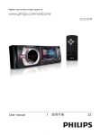
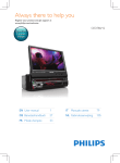
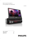
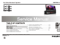
CED780/51/55/98
Car Entertainment System
SPECIFICATIONS...............................................................................1-1
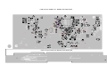
MAIN & MCU PCB COMPONENT LAYOUT...................................14-15
SERVO PCB COMPONENT LAYOUT.............................................16-17
PANEL&BT PCB COMPONENT LAYOUT.......................................18-19
PANEL TFT&SD PCB COMPONENT LAYOUT...............................20-21
CIRCUIT DIAGRAM MAIN&MCU&TUNER BOARD...........................5-8
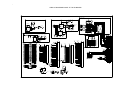
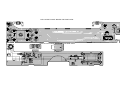
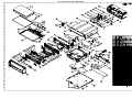
SET EXPLODER VIEW DRAWING.................................................22
CIRCUIT DIAGRAM SERVO BOARD.................................................9
CIRCUIT DIAGRAM PANEL& BT BOARD........................................10-11 TROUBLE SHOOTING ...................................................................23
CIRCUIT DIAGRAM PANEL TFT & SD BOARD...............................12-13
Published by JOEY_SL
Version 1.1
WK1147
BG LE Printed in The Netherlands
Subject to modification
314178536641
1-1
SPECIFICATIONS
General
Power supply
Fuse
Suitable speaker
impedance
Maximum power
output
Continuous power
output
Pre-Amp output
voltage
Subwoofer output
voltage
Aux-in level
Dimensions (W x H
x D)
Weight (main unit)
LCD
12 V DC (11 V - 16 V),
negative ground
15 A
4-8
50 W x 4 channels
24 W x 4 channels
(4 10% T.H.D.)
4.0 V ( CD play mode;
1 kHz, 0 dB, 10 k
load)
4.0 V (CD play mode,
61 Hz, 0 dB, 10 k
load)
500 mV
178 x 50 x 210 mm
3.1 kg
Screen size
Display resolution
Contrast ratio
Brightness
7.0 inches
800 x 480 dots
500
450 cd/m2
Supported MP3 disc format:
Bluetooth
Communication
system
Output
Maximum
communication
range
Frequency band
Bluetooth Standard version
2.0
Bluetooth Standard Power
Class 2
Line of sight approx. 8m
2.4 GHz band (2.4000 GHz
- 2.4835 GHz)
Compatible
Bluetooth
Advanced Audio
Audio Video Remote
Disc player
System
Frequency response
Signal/noise ratio
Total harmonic
distortion
Channel separation
Video signal format
Video output
DVD / CD audio /
MP3 system
20 Hz - 20k Hz
>75dB
Less than 1%
>55dB
NTSC only
1 +/- 0.2V
Supported
codecs
Receive
Transmit
SBC (Sub Band Codec)
SBC (Sub Band Codec)
Playability information
Compatible USB devices:
Radio
Frequency range - FM
Frequency range AM(MW)
Usable sensitivity - FM
Usable sensitivity - AM
(MW)
87.5 - 108.0 MHz
(50kHz per step)
522 - 1620 KHz
(9kHz per step)
5 uV
25 uV
length: 128 bytes)
Supported USB formats:
variable bit rate
levels
44.1kHz, 48 kHz
variable bit rate
Supported video formats:
The following video formats(containers) are supported on current product:
•
MPEG1 (*.avi, *.mpg, *.dat)
•
MPEG4 (simple profile) (*.avi)
•
DIVX4 (*.avi)
•
DIVX5 (*.avi)
•
XVID (*.avi)
NOTE:
To ensure smooth playback, the image size should not be higher than 640X480,
frame rate should not be higher than 20 fps and data rate should not be
higher than 500kbps in the encoded video.
Unsupported video formats:
The following video formats(containers) cannot be supported on current product:
•
M-JPEG (*.avi, *.mov)
•
MPEG4 (*.mov, *.wmv, *.mp4, *.3g2, *.asf, *.3gp)
•
H.263 (*.avi, *.mov, *.flv, *.3gp)
•
H.264 (*.mp4, *.mov)
•
WMV3 (*.wmv, *.avi)
•
WMV2 (*.wmv)
•
RealVideo4 (*.rmvb, *.rm)
•
RealVideo3 (*.rm)
•
RealVideo2 (*.ram)
•
MS Video (*.avi)
NOTE:
For format(container) not listed above, it is not guaranteed to work.
Please avoid from using with the product.
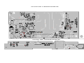
CED780 Dismantlement Method
1. Take out the three screws at heat sink, the six screws at the left right side of the main unit and the screw at the base panel
7DNHRXWWKHVFUHZVDWKHDWVLQN
7DNHRXWWKHVFUHZVDWWKHOHIWVLGHRIWKHXQLW
7DNHRXWWKHVFUHZVDWWKHULJKWVLGHRIWKHXQLW
7DNHRXWWKHVFUHZDWEDVHSDQHO
2. Prize up the left right hook of the base panel and take out the base panel, separate the bottom cover from the unit
ϟय़
3UHVVGRZQZDUG
Ϟ᪀䍋
3UL]HXS
ϟय़
3UHVVGRZQZDUG
'LVDVVHPEOHWKHOHIWVLGHRIWKHEDVHSDQHO
ᢚߎᥦ㒓
7DNHRXWWKH))&
Ϟ᪀䍋
3UL]HXS
'LVDVVHPEOHWKHULJKWVLGHRIWKHEDVHSDQHO
'LVDVVHPEOHWKH))&DWEDVHSDQHO
'LVDVVHPEOHWKHWRSFRYHU
6HSDUDWHWKHFRPSRQHQWRIWKHEXWWRQFRYHU
3. Take out the FFC which connect to main board, and take out the fixed screws of the back cover, then take out the FFC at the deck mechanism
7DNHRXW))&
7DNHRXWWKHVFUHZVDWGHFNPHFKDQLVP
/LIWXSGHFNPHFKDQLVP
'LVDVVHPEOHWKH))&DWGHFNPHFKDQLVP
'LVDVVHPEOHGHFNPHFKDQLVP
4.Disassemble black wire and FFC first, then take out the screws around TFT
偀䖒㒓
0RWRUZLUH
⬉ᄤ㒓
:LUH
7DNHRXWWKHZLUHDQGPRWRUZLUH
'LVDVVHPEOHWKH))&
7DNHRXWWKHVFUHZVDURXQG7)7
2
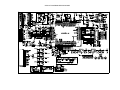
BLOCK DIAGRAM
CED780(B) Block Diagram --S3C2451 & CS4728 Solution
Deck (Chu Dong)
USB Host
IPHONE
Pickup Sanyo 860
Motor Driver
5888
I²S or
S/PDIF
DVD
(SUNPLUS SPHE8202G)
SDRAM
Cirrus
CS47048
(100 pin )
Power Amplifier
Sanyo LV47002P
Flash
SPI 2
Subwoofer
output
4558
X2
Front Rear
Audio output
16 Pin
Connector
CS4344
A/D
Front PanelTFT
(800x480) With TCON
Radio Tuner
I²S
SPI 1
SI474X
4558
I²C
Front Panel
Variable-Color
Illumination
SPI 1
MCU ST8
64Pin 128k
Samsung
S3C2451
UART 2
PT6579LQ
|hy{GzGGG
PI5C3303
|hy{GGp¸j
BT UART 1
ADV7180
48Pin
DVD CVBS
Front AUX Input
GPS(SIRFIII )
DVD YUV
External Ready
CAMERA
AV IN Rear
DVI
FM6502
24Pin
Video output 1
Video output 2
AV IN Front
I² C
GPS BOX
Audio out
3
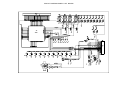
WIRING DIAGRAM
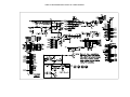
4
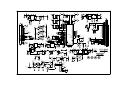
CIRCUIT DIAGRAM-MAIN & MCU & TUNER BOARD
5
6
7
8
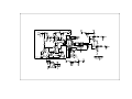
CIRCUIT DIAGRAM-SERVO BOARD
9
CIRCUIT DIAGRAM-PANEL & BT BOARD
10
11
CIRCUIT DIAGRAM-PANEL TFT & SD BOARD
SD CARD (GPS)
VDD_3.3V
C132
104
GTXD GTXD1 GRXD GRXD1
9
8
GND1
GND2
CON12
GND3
VDD5V
DN
DP
NC
GND
10K
1
2
3
4
CS4344
OUTL
4
3
2
1
10K x 4
7
8
5
RN10
4
3
2
1
RN9
10K x 4
5
SDCLK
SDCMD
SDDAT0
SDDAT1
R75
RN5
33R x 4
11 GND
10 GND
8
7
5
6
5
C128 C125 C124 C127 C221
C113
10
10pF 10pF 10pF
10pF
10pF
22U/10V
6
OUTR
7
FILT+
C131
3.3VD
R142
R143
R144
10K
10K
10K
NTRST
GGND
7
GGND1
VDDRTC
J7-B
VDD_OP123V
J7-D
TDI
33R
DVD_DI
R70
33R
IICSCL
R106
SDA
R42
33R
IICSDA
DN0
DP0
R15
33R
R16
L_CS
R72
L_SCL
R77
L_SDI
R78
VIB_CTL
STDBY_CTL
GTXD
33R
GPL5
33R
GPL4
33R
GPA1
33R
NC
R162
GPB0
33R
R160
TXD0
R135
33R
R153
33R
GPB3
R154
33R
VCLK
HSYNC
R157
33R
VSYNC
R158
33R
GRXD
BRT/PWM
PCLK
DE
RXD
0R
R34
R39
8
7
ALRCIN
AXDI
5
RN1
100R x 4
C6
1
2
3
4
EINT21/GPG13
EINT22/GPG14
EINT23/GPG15
VM
TXD2
EINT16/GPG8
EINT9/GPG1
EINT8/GPG0
EINT6/GPF6
IICSCL
IICSDA
EINT4/GPF4
EINT3/GPF3
EINT2/GPF2
EINT1/GPF1
EINT0/GPF0
6
GPB3
GPB2
GPB1
GPB0
TSXP
TSXM
TSYP
TSYM
AIN0
NSS1
NSS0
SPICLK1
SPICLK0
SPIMOSI1
SPIMOSI0
SPIMISO1
SPIMISO0
RXD2
NC
VDD_3.3V
R49
10K
1.3VD
CDCLK
BATT_FLT
PWR_EN
NTRST
I2SSDO
I2SSCLK
I2SLRCK
4
5
5
TCK
7
R11
0R
1.2VD
USB1.2V
VDD_3.3V
J7-C
R108
0R
SDCLK
SDCMD
SDDAT0
SDDAT1
SDDAT2
SDDAT3
NCD_SD
WP_SD
TXD0
RXD0
TXD1
RXD1
TXD2
RXD2
NTRST
TCK
TDI
TDO
TMS
RTCK
EINT5/GPF5
EINT19/TCLK1
R8
NC
VLCD 1.2VD
GPA7
GPA8
GPA9
GPH6/TXD3
GPH7/RXD3
R110
0R
80
81
82
83
84
85
86
87
88
89
90
91
92
93
94
95
96
97
98
99
100
101
102
103
104
105
106
107
108
109
110
111
LEND/GPC5
VCLK
VLINE
7
RTCK
8
VFRAME
VM
LCD_PWREN
8
TDO
9
RED7
RED6
RED5
RED4
RED3
RED2
RED1
RED0
GRN7
GRN6
GRN5
GRN4
GRN3
GRN2
GRN1
GRN0
BLUE7
BLUE6
BLUE5
BLUE4
BLUE3
BLUE2
BLUE1
BLUE0
GPA1
GPA2
GPL4
GPL5
GPL6
GPL7
EINT12/GPG4
3.3VD
TDI
RTCK
TDO
R145
GND1
NC
DC+5V
5
4
TSXM
3
TSYM
2
TSXP
1
TSYP
CON4
YP XP YM XM
6
TKEY2_DAT
VLED-
96
10
10
11
11
12
12
13
13
14
14
15
15
16
16
17
17
18
18
19
19
20
20
BK Socket
4
2
21
21
3
1
22
22
23
23
24
24
CON10
VLED+
6
VDD_3.3V
R93
RT9819C-30PVL
15pF
3
ADIN
ABLCK
VLINE
33R
R14
REDA4
REDA5
REDA6
REDA7
EINT20/GPG12
VFRAME
33R
R163
TXD
RXD0
33R
R159
CHREF
CPCLK
CSCLK
CRESET
REDA0
REDA1
REDA2
REDA3
GPB2
NC
R161
CVSYNC
GPA2
6
U6
R141
VCC
R69
AIN0
7
8
9
10
11
12
13
14
15
16
17
18
19
20
21
22
23
24
25
26
27
28
29
30
31
32
OUT
LNRESET
NC
1
2
3
4
5
DN1
DP1
I2SSDO
I2SSDI
CDCLK
I2SSCLK
I2SLRCK
EINT0/GPF0
GND
R166
EINT2/GPF2
0R
1
BK_SENSOR
33R
2
USB_CHK
3
4
NTRST
TMS
TCK
1.0K-4P
J7-A
R36
SCL
WAKE
GPE6/AC_SDI
GPE9/AC_RST
112
113
114
115
116
117
118
119
120
121
122
123
124
125
126
127
128
129
130
131
132
133
134
135
136
137
138
139
140
141
142
143
144
145
146
147
148
149
150
151
152
153
154
155
156
157
158
GPS_MODULE-PCB
SPIMISO0
VDD_MEM
USB3.3V
GPS_MODULE-PCB
DVD_DO
C150
4R7
DN0 DP0
10K
NTRST
C54
104
4
104
DN0
NTRST
DP0
R169
NC
R170
NC
3
2
CON7
DVD_CLK
33R
GPS_MODULE-PCB
33R
R37
6
R41
33
34
35
36
37
38
39
40
41
42
43
44
45
46
47
48
49
50
51
52
53
54
55
56
57
58
59
60
61
62
63
64
65
66
67
68
69
70
71
72
73
74
75
76
77
78
79
GPS_MODULE-PCB
TMS
SPICLK0
2
3
3V3
GRXD
CON6
0.5-24P
1
2
GTXD
GND4
SPIMOSI0
CON9
0.5-24P
1
10U/0805
6
1
2
3
4
5
9 D2
8 CD/D3
7 CMD
VDD
5 CLK
4 VSS
3 D0
2 D1 CON1
1 CD SD MINI
6
12 GND
13 GND
8
7
8
G+5V G+5V1
USB-SOCKET-MINI
47pF
RN6
33R x 4
26
C133
10U/0805
1R0
C82
NC
1
2
3
4
25
6
DC+5V
DIN
DEM/BCK
LRCK
MCLK
VQ
R20
C81
NC
VA
1
2
3
4
5
C116
NC
SDDAT2
SDDAT3
NCD_SD
WP_SD
26
U2
22U/10V 104
5
OUTR
FL_OUT
6
GND4
C111
GPS_AUDIO
V_DAC
USB+
GND2
R2
T28
1uF
T27
C70
R23
4R7
25
33K
R173
22U/10V
6
18K
R172
1
2
3
4
5
C79
C73
8
OUTL
DIN
DEM/BCK
LRCK
MCLK
AGND
8
9
VDD5V
DN
DP
NC
GND
7
GND3
GND1
1
2
3
4
ALRCIN
AXDI
USB_CHK
0R
C67
104
3.3VD
6
ADIN
ABLCK
R168
0R
9
R167
USB-SOCKET-MINI
GND
DEVICE
CON3
CS4334
VA
U1
7
8
DP1
7
DN1
GND2
FB15
DC+5V
B221
DP1
DN1
V_DAC
R94
33R
R95
33R
TXD1
RXD1
1
12
22U/10V 104
C13
330P
330P
33K
3 R33
C44
104
35
C53
104
36
C52
104
46
C37
104
47
C19
104
48
C18
104
49
C39
102
50
C59
10U/0805
4
104
C61
104
C122
104
C62
10U/0805 39
C68
104
C69
10U/0805
R85
R38
R58
10K
330R 2
R28
R57
4
27P
SCL SDA
PNL_CLOSE
PNL_OPEN
2K2
U5
RT9013-12PB
DC+5V
1
PNL+12V
R12
C42
1uF
VIN
1.2VD
2
VSS
3
EN
10K
C26
C28
104
22U/10V
EN
VIN
U8
BP
4
C49
22U/10V
C43
104
1uF
R7
VIN
VOUT
2
VSS
AIN6
CAPC2
CAPY2
CAPY1
3
EN
NC
VDD18
4
C50
CRESET
C46
2
LX
3
22U/10V
104
ELPF
R47
T38
FB2
VDD_3.3V 3.3VD
B600
B600
FB3
VDD_MEM
C45
R101
C60
22PF
150K
10U/0805
C30
C1
C2
22U/10V
104
104
C115
104
C27
FB
C8
104
22U/10V
104
51
VTFT
B221
T5
C56
C55
T4
22U/10V
104
RED7
RED6
RED5
RED4
RED3
RED2
RED1
RED0
GRN7
GRN6
GRN5
GRN4
GRN3
GRN2
GRN1
GRN0
BLUE7
104
1K5
R76
C57
13
12
8
7
6
5
62
61
60
59
104
4K7
REDA0
REDA1
T8
VSYNC
HSYNC
T7
REDA2
REDA3
REDA4
20
R55
REDA5
REDA6
REDA7
33R
55
56
63
64
2
9
R4
NC
R5
NC
47pF
47pF
VD_18P
823
BLUE3
3.3VD
103
C129
BLUE2
BLUE1
BLUE0
T6
PCLK
C25
VGH
VGL VD_10V4
10K
10K
R113
R112
DC+5V
R/L
U/D
10pF
T1
VGH
R117
30
0R/0805 C93
C65
Z4
C23
BLUE6
BLUE5
BLUE4
CHREF
C123
34
C22
CPCLK
CVSYNC
NC 22U/10V
10U/0805
C11
C15
C71
C66
C72
104
104
104
LNRESET
VCOM
R91
10K
10U/0805
C21
FB4
C86
VDDRTC
D19
R176
4R7
C32
C92
1
2
3
4
5
6
7
8
9
10
11
12
13
14
15
16
17
18
19
20
21
22
23
24
25
26
27
28
29
30
31
32
33
34
35
36
37
38
39
40
41
42
43
44
45
46
47
48
49
50
VLED+
VLED+
VLEDVLEDGND
VCOM
DVDD
MODE
DE
VS
HS
B7
B6
B5
B4
B3
B2
B1
B0
G7
G6
G5
G4
G3
G2
G1
G0
R7
R6
R5
R4
R3
R2
R1
R0
GND
DCLK
GND
L/R
U/D
VGH
VGL
AVDD
RESET
NC
VCOM
DITHB
GND
NC
NC
C90
NC
220U/16V 4U7/0805
12.4K/1%
C109
130K
100K
C110
22U/10V
R102
1R0
AMS1117-3.3V
VIN
C20
PNL+12V
M_VCC
22U/10V
VDD33
FB7
C4
VOUT
104
VGL
B600
C3
C7
22U/10V
LX
2
3
T17
22uH
6
R174
GND
OVP 5
10K
FB
EN
VDD
C126
T24
T25
PT8
T26
PT7 PT6 PT5
PT4 PT3 PT2
PT1
C78
104 10U/0805
4
H1 H2 H3 H4 H5 H6 H7 H8 H9 H10
U12
104
3.3VD T39
VOUT
1
RT9293B
R114
360R
U16
B5819WS
DC+5V
1uF
L16
R175
VLCD
B221
104
22U/10V
DC+5V
C31
10U/0805
R74
C24
B600 VDD_OP123V
C12
3R9/0805
VCOM
22U/10V
R10
3.3VD
3.3VD
FB1
R65
C63
FB5
10K
4.7uH
R6
R92
3.3VD
DC+5V
VD_10V4 T30
LDC1006
VLED-
3R9/0805
33
45
NC
NC
ALSB
SCLK
SDATA
VDD_OP123V
1.3VD 3.3VD
L5
T20
10U/0805
223
1
GND
3
R81
1
INT
RESET
PWRDWN
52
54
53
C36
LLC
VS_IN
HS_IN/CS_IN
FIELD/DE
VS
HS/CS
SFL/SYNC_OUT
XTAL
XTAL1
51
10K 29
5
U7
ADV7181C
CML
REFOUT
104
R48
P10
P11
P12
P13
P14
P15
P16
P17
P18
P19
SOG/SOY
42
T37
10K
2
FB
RT9293B
B221
28
27
26
25
19
18
17
16
15
14
P0
P1
P2
P3
P4
P5
P6
P7
P8
P9
4K7
5 VFB
4
1
33R
33R
NC
R26
DC+5V
U4
RT9193-18PB
DC+5V
C35
10U/0805 41
22U/10V
AIN5
VD_33D
R59
R60
5
C34
104
C75
104
AIN4
22
21
2K2
T36
VOUT
C74
C76
28.6363MHZ
GND
L3
3
C83
IICSCL
IICSDA
+12V
4
1M
STR-ST105
WAKE
X2
2
33K
3 R35
103
4K7
C80
1
U11
1
C10
27P
T11
C120
AIN3
38
VDD33
DVD_DI
DVD_DO
DVD_CLK
R84
AIN2
44
C121
STR-ST105
PNL_SEN3
ESD5V
ESD5V
AIN1
3
10
24
57
330R 2
C105
104
4
11
T10
U10
C77 C98
R46
C14
GND
EN
52
330P
4
1
R25
DZ1
DZ2
FB10
4
B5819WS
330P
T40
PNL_SEN1
PNL_SEN2
PNL_SEN3
5 OVP
BRT/PWM
C64
D16
BAT54S
C+5V
TKEY2_DAT
B221
C97
STR-ST105
PNL_SEN2
C58
1uF
R32
330R 2
R17
PS_U
C29
22U/10V
VDD18
1
40
31
C38
75R
PNL_V/Y
VD_18P
T19
VLED+
B5819WS
LX
VDD
100K
L7 3.3uH
33K
3 R31
22U/10V
1.69K/1%
U9
1
6.8uH
22U/10V 104
R116
1K5/0805
R115
C96
3V6
C9
5R6
T2
C102
1uF
Z3
C101
4u7/0805
22U/10V
1PX1
1PX2
1PX3
1PX4
FIDUCIAL
FIDUCIAL
FIDUCIAL
FIDUCIAL
D17
BAT54S
DC+5V
Q22
R129
560R
R137
560R
D3
R52
180R R182
220R R183
330R
SW1
KEY2
104
SW3
NC R50
C48
560R
U13
2K2
R104
ZD5
6V8
R109
Q24
10K
D11
1N4148
D21
1N4148
R3
9015
Q27
9014
BIN 2
PNL_CLOSE
AIN 3
PNL_OPEN
NC 4
M_VCC
GND 5
22K
22K
???
TKEY2_DAT
1R0/1206
NC 1
R1
104
D13
R138
R99
C47
D12
???
C+5V
2SD882
SW2
37
C41
PS_V/C
T9
104
104
D14
22uH
U3
R66
C
GPS_AUDIO
T16
FB13
L6 3.3uH
75R
PNL_SEN1
???
T21
T22
T23
T29
T31
T32
V
104
VD_33D
C+5V
DC+5V
GTXD
GRXD
RXD
TXD
22U/10V
L4
6
75R
6K8
B221
PS_V/C
330P
PS_U
DC+5V
FB6
330P
VDD33
R21
R24
38
36P-0.5-TFT
T13
T12
T14
T18
100U/10V
20K
1
2
3
4
5
6
7
8
9
10
11
12
13
14
15
16
17
18
19
20
21
22
23
24
25
26
27
28
29
30
31
32
33
34
35
36
T3
C112
332
NC
CON2
C16
22U/10V
30K
C85
C87
C88
22U/10V
FB11 B600
C139
D2
R22
NC
C114
C119
23
58
D1
C17
C118
AVDD
PVDD
5
C40
C117
AGND
AGND
AGND
FB
L2
+5V
B600
32
37
43
6
104
SW
22UH/1A2
6.8uH
DVDD
DVDD
U14
RT8284N
L1
VDD33
FB14
R63
DVDDIO
DVDDIO
1
2
SYNC
BS
EN
8
103
VD_33A
B221
L8 3.3uH
PNL_V/Y
DGND
DGND
DGND
DGND
100K
C51
3
GND
104
7
Y
DC+5V
4
220U/16V
VIN
R44
C5
COMP
C33
+5V
T15
TFT_TM070RDH11
VD_18D
FB9
C84
CON8
VDD18
+12V
VCC 6
T35
BOUT 7
M+
AOUT 8
M-
NC 9
CMD6208
T33
CON5
MOTOR
T34
13
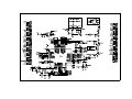
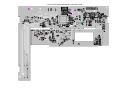
PCB LAYOUT-MAIN BOARD TOP SIDE VIEW
PCB LAYOUT-MCU BOARD TOP SIDE VIEW
14
PCB LAYOUT-MAIN BOARD BOTTOM SIDE VIEW
PCB LAYOUT-MCU BOARD BOTTOM SIDE VIEW
15
PCB LAYOUT-SERVO BOARD TOP SIDE VIEW
16
PCB LAYOUT-SERVO BOARD BOTTOM SIDE VIEW
17
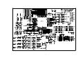
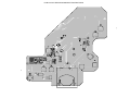
PCB LAYOUT-PANEL BOARD TOP SIDE VIEW
PCB LAYOUT-PANEL BT BOARD TOP SIDE VIEW
18
PCB LAYOUT- PANEL BOARD BOTTOM SIDE VIEW
PCB LAYOUT- PANEL BT BOARD BOTTOM SIDE VIEW
19
PCB LAYOUT-PANEL TFT BOARD TOP SIDE VIEW
PCB LAYOUT-PANEL SD BOARD TOP SIDE VIEW
20
PCB LAYOUT-PANEL TFT BOARD BOTTOM SIDE VIEW
PCB LAYOUT- PANEL SD BOARD BOTTOM SIDE VIEW
21
SET EXPLODER VIEW DRAWING
440-0C352499-00-00
22
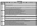
Trouble shooting
Product Model
CED780
Area
All area
failure
Tate
2011-11-28
failure cause
NO. phenomena
remark
a. To check whether the CN2(14pin) connector of the tail of the unit is connect well , Whether it is loose of the 15A fuse of the
Filter Box, or insert non in place.
b. To check whether there is any contamination and bad contact on the 24 Pin male/female connector on the panel and main
board.
1
NO Power
c. To check the U3 of multiple voltage regulator IC,the 9 pin should be +12V0
be +3V3 the 13 pin should be +8V5 the 14 pin should be +5V0.
the 10 pin should be +5V0
the 1 pin should
d. To check the 7 pin voltage of the U2(MCU) should be +5V0.
e. To check the oscillation frequence of crystal X1 shuold be 16MHz .
a.To check the connectors of the CON6
CON9
whether the socket of it is loose.
b.To Check the voltage of the 33 pin~36 pin of the CON2 ,should be +12V0
2
7"TFT c.To check the voltage of the L2 of the TFT board,should be +5V0.
abnormal d.To check the voltage of the cathode of the D14 of the TFT board,should be +10V0.
e.If the TFT move defective, to check the U13(6208 IC) and the U9~U11 of the photo reflective, to check whether there is any
abnormal of the rotation of the TFT mechanism.
a. To check whether the volume knob is turn to the minimum position.
b. To check whether the unit is at MUTE mode, press SOURCE button and check whether it is effective of the input sound
source.
3
NO audio
c. To check whether the connection of 8 PIN audio output wire of ISO connector is correct; wrong connection or short circuit
output
to the ground will caused the protection of the power amplifier( no voltage output).
d . To check the circuit of power amplifier U12(LV47002 IC) and VOLUME U7(47048 IC).
e. To check the voltage of 22 PIN(MUTE) of power amplifier U12(47002 IC) , normally should be 4V0.
a. To check the antenna of the AM/FM tuner.
4
b. To check whether the strength of then input signal of the tuner is too weak.
Radio
abnormal c. To check the voltage of the 13 pin of the U8 of the tuner IC, should be +3V3.
d. To check the oscillation frequence of crystal X3 of the tuner IC,shuold be 32.768MHz
23
NO.
failure
phenomena
failure cause
remark
a. To check whether the signal format of the disc is correspond to the request of the unit, whether there is any
contamination or damage or light leakage on the surface of the disc.
b. To check whether there is any abnormal of the rotation of the deck mechanism, or whether the disc is enter in
position.
c. To check whether it is normal when reading USB?
d. To check whether the 24P FFC of laser pick up is inserted in place, whether the socket of it is loose.
5
CD/DVD
defective
e. To check whether there is any contamination or foreign body on the surface of the laser pick up.
f. To check the servo board connector of CN3 and the main board connector of CN1, whether the socket of it is loose.
g.To check the voltage of the 9 pin ~ 12 pin of the CN1 , should be +5V0.
h. To check the switch SW1 on the servo board.
i. To check the rotation mechanism of CD/DVD deck.
a. To check whether the USB/SD signal format is correspond to the request of the unit.
b. To check the voltage of the USB connector of the left first pin , should be +5V.
6
USB/SD
defective
c. To check whether there is any wearing and scratch of the shrapnel and pin of the panel USB.
d. To check the servo board connector of CN3 and the main board connector of CN1, whether the socket of it is loose.
e.To check whether there is any contamination and bad contact on the male/female connector of the panel and main
board. If necessary, can exchange the panel to test whether the defective is occurred by the unit or panel.
a. To check the SOURCE shoule be in MP3-LINK mode.
7
AUX defective
b. To check the AUX IN input signal.
c. To check whether there is any contamination and bad contact on the male/female connector of the panel and main
board. If necessary, can exchange the panel to test whether the defective is occurred by the unit or panel.
a、Check the unit should be in pair with the BT phone connection status
8
BT defective b、To check the 9 pin of the BT module,should be +3V3、
c、To check the CN8 connector、
a、To check the micro SD memorizer of the map of the GPS、
9
GPS defective b、To check the GPS antenna of the tail of the unit、
c、To check the connectors of the CON2
CON8
CON9
whether the socket of it is loose、
24