1
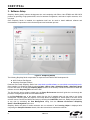
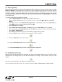
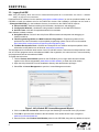
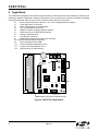
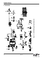
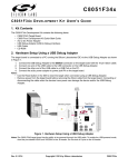
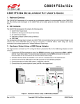
C8051F32x C8051F32 X D EVELOPMENT K IT U SER ’ S G U I D E 1. Kit Contents The C8051F32x Development Kit contains the following items: • • • • • • C8051F320 Target Board C8051Fxxx Development Kit Quick-Start Guide AC to DC Power Adapter USB Debug Adapter (USB to Debug Interface) USB Cable CD-ROM 2. Hardware Setup Using a USB Debug Adapter The target board is connected to a PC running the Silicon Laboratories IDE via the USB Debug Adapter as shown in Figure 1. 1. 2. 3. 4. Connect the USB Debug Adapter to the DEBUG connector on the target board with the 10-pin ribbon cable. Connect one end of the USB cable to the USB connector on the USB Debug Adapter. Connect the other end of the USB cable to a USB Port on the PC. Connect the ac/dc power adapter to power jack P1 on the target board. Notes: • Use the Reset button in the IDE to reset the target when connected using a USB Debug Adapter. • Remove power from the target board and the USB Debug Adapter before connecting or disconnecting the ribbon cable from the target board. Connecting or disconnecting the cable when the devices have power can damage the device and/or the USB Debug Adapter. AC/DC Adapter PC Target Board USB Debug Adapter PWR SILICON LABORATORIES RESET P3.7 Run Stop Silicon Laboratories USB DEBUG ADAPTER Power USB Cable MCU P1.6 Port 2 Port 0 Port 1 Port 3 Port 4 Figure 1. Hardware Setup Using a USB Debug Adapter Note: The C8051F320 target board has the ability to be powered through the USB cable. To enable the USB-powered mode, move the shorting block located at header J2 to header J11. Rev. 0.9 2/14 Copyright © 2014 by Silicon Laboratories C8051F32x C8051F32x 3. Software Setup Simplicity Studio greatly reduces development time and complexity with Silicon Labs EFM32 and 8051 MCU products by providing a high-powered IDE, tools for hardware configuration, and links to helpful resources, all in one place. Once Simplicity Studio is installed, the application itself can be used to install additional software and documentation components to aid in the development and evaluation process. Figure 2. Simplicity Studio The following Simplicity Studio components are required for the C8051F320 Development Kit: 8051 Products Part Support Simplicity Developer Platform Download and install Simplicity Studio from www.silabs.com/8bit-software or www.silabs.com/simplicity-studio. Once installed, run Simplicity Studio by selecting StartSilicon LabsSimplicity StudioSimplicity Studio from the start menu or clicking the Simplicity Studio shortcut on the desktop. Follow the instructions to install the software and click Simplicity IDE to launch the IDE. The first time the project creation wizard runs, the Setup Environment wizard will guide the user through the process of configuring the build tools and SDK selection. In the Part Selection step of the wizard, select from the list of installed parts only the parts to use during development. Choosing parts and families in this step affects the displayed or filtered parts in the later device selection menus. Choose the C8051F32x family by checking the C8051F32x check box. Modify the part selection at any time by accessing the Part Management dialog from the WindowPreferencesSimplicity StudioPart Management menu item. Simplicity Studio can detect if certain toolchains are not activated. If the Licensing Helper is displayed after completing the Setup Environment wizard, follow the instructions to activate the toolchain. 2 Rev. 0.9 C8051F32x 3.1. Running Blinky Each project has its own source files, target configuration, SDK configuration, and build configurations such as the Debug and Release build configurations. The IDE can be used to manage multiple projects in a collection called a workspace. Workspace settings are applied globally to all projects within the workspace. This can include settings such as key bindings, window preferences, and code style and formatting options. Project actions, such as build and debug are context sensitive. For example, the user must select a project in the Project Explorer view in order to build that project. To create a project based on the Blinky example: 1. Click the Simplicity IDE tile from the Simplicity Studio home screen. 2. Click the Create new project link from the welcome screen or go to FileNewSilicon Labs MCU Project. 3. In the Kit drop-down, select C8051F320 Development Kit, in the Part drop-down, select C8051F320, and in the SDK drop-down, select the desired SDK. Click Next. 4. Select Example and click Next. 5. Under C8051F320 Development Kit in the Blinky folder, select F320-1 Blinky and click Finish. 6. Click on the project in the Project Explorer and click Build, the hammer icon in the top bar. Alternatively, go to ProjectBuild Project. 7. Click Debug to download the project to the hardware and start a debug session. 8. Press the Resume button to start the code running. The LED should blink. 9. Press the Suspend button to stop the code. 10. Press the Reset the device button to reset the target MCU. 11. Press the Disconnect button to return to the development perspective. 3.2. Simplicity Studio Help Simplicity Studio includes detailed help information and device documentation within the tool. The help contains descriptions for each dialog window. To view the documentation for a dialog, click the question mark icon in the window: This will open a pane specific to the dialog with additional details. The documentation within the tool can also be viewed by going to HelpHelp Contents or HelpSearch. Rev. 0.9 3 C8051F32x 3.3. Legacy 8-bit IDE Note: Using the Simplicity Studio tools with the C8051F320 Development Kit is recommended. See section 3. "Software Setup‚" on page 2 for more information. Download the 8-bit software from the website (www.silabs.com/8bit-software) or use the provided installer on the CD-ROM to install the software tools for the C8051F32x devices. After installation, examples can be found in ...\Examples\C8051F320_1 in the installation directory. At a minimum, the C8051F320 DK requires: Silicon Labs IDE—Software enabling initial evaluation, development, and debugging. Wizard 2—Initialization code generation software for the C8051F32x devices. Keil C51 Tools—Keil 8051 Compiler/Assembler/Linker toolchain. Other software available includes: Configuration Keil µVision Driver—Driver for the Keil µVision IDE that enables development and debugging on C8051Fxxx MCUs. Flash Programming Utilities and MCU Production Programmer—Programming utilities for the production line. More information on the available programming options can be found on the website: http://www.silabs.com/products/mcu/Pages/ProgrammingOptions.aspx. ToolStick Development Tools—Software and examples for the ToolStick development platform. More information on this platform can be found at www.silabs.com/toolstick. The development kit includes the latest version of the C51 Keil 8051 toolset. This toolset is initially limited to a code size of 2 kB and programs start at code address 0x0800. After registration, the code size limit is removed entirely and programs will start at code address 0x0000. To register the Keil toolset: 1. Find the Product Serial Number printed on the CD-ROM. If you no longer have this serial number, register on the Silicon Labs website (www.silabs.com/8bit-software) to obtain the serial number. 2. Open the Keil µVision4 IDE from the installation directory with administrative privileges. 3. Select FileLicense Management to open the License Management window. Figure 3. Keil µVision4 IDE License Management Window 4. Click on the Get LIC via Internet... button to open the Obtaining a License IDE Code (LIC) window. 5. Press OK to open a browser window to the Keil website. If the window doesn’t open, navigate to www.keil.com/license/install.htm. 6. Enter the Silicon Labs Product Serial Number printed on the CD-ROM, along with any additional required 4 Rev. 0.9 C8051F32x information. 7. Once the form is complete, click the Submit button. An email will be sent to the provided email address with the license activation code. 8. Copy the License ID Code (LIC) from the email. 9. Paste the LIC into the New License ID Code (LIC) text box at the bottom of the License Management window in µVision4. 10. Press the Add LIC button. The window should now list the PK51 Prof. Developers Kit for Silabs as a licensed product. 11. Click the Close button. Rev. 0.9 5 C8051F32x 4. Target Board The C8051F32x Development Kit includes a target board with a C8051F320 device pre-installed for evaluation and preliminary software development. Numerous input/output (I/O) connections are provided to facilitate prototyping using the target board. Refer to Figure 4 for the locations of the various I/O connectors. P1 Power connector (accepts input from 7 to 15 VDC unregulated power adapter) J1 36-pin Expansion I/O connector J2 Power Target Board from power adapter J3 Port I/O Configuration Connector J4 DEBUG connector for Debug Adapter interface J5 DB-9 connector for UART0 RS232 interface J6 Analog I/O terminal block J7 Low pass filter connector J8 USB Debug Adapter target board power connector J9, J10 External crystal enable connectors J11 Power Target Board from USB J12 Connects external capacitance to P0.7 J13 Connects R14 Potentiometer to P1.7 J14 USB connector for USB interface P2.1 P2.0 RESET J5 R14 Pin 2 J13 Pin 1 Pin 2 P2.2 Pin 1 J1 P2.3 Prototype Area J9 J3 DEBUG J10 J8 C8051 F32X J4 J7 J12 P1 J14 J11 J2 J6 PWR Pin 1 Prototyping Area I/O Connection Points Figure 4. C8051F320 Target Board 6 Rev. 0.9 Pin 1 C8051F32x 4.1. System Clock Sources The C8051F320 device installed on the target board features a calibrated programmable internal oscillator which is enabled as the system clock source on reset. After reset, the internal oscillator operates at a frequency of 1.5 MHz (±1.5%) by default but may be configured by software to operate at other frequencies. Therefore, in many applications an external oscillator is not required. However, if you wish to operate the C8051F320 device at a frequency not available with the internal oscillator, an external crystal may be used. Refer to the C8051F32x data sheet for more information on configuring the system clock source. The target board is designed to facilitate the installation of an external crystal. Remove shorting blocks at headers J9 and J10 and install the crystal at the pads marked Y1. Install a 10 M resistor at R9 and install capacitors at C14 and C15 using values appropriate for the crystal you select. Refer to the C8051F32x data sheet for more information on the use of external oscillators. 4.2. Switches and LEDs Three switches are provided on the target board. Switch SW1 is connected to the RESET pin of the C8051F320. Pressing SW1 puts the device into its hardware-reset state. Switch SW2 and SW3 are connected to the C8051F320’s general purpose I/O (GPIO) pins through headers. Pressing SW2 or SW3 generates a logic low signal on the port pin. Remove the shorting blocks from the header to disconnect SW2 and SW3 from the port pins. The port pin signals are also routed to pins on the J1 I/O connector. See Table 1 for the port pins and headers corresponding to each switch. Three LEDs are also provided on the target board. The red LED labeled PWR is used to indicate a power connection to the target board. The green LEDs labeled with port pin names are connected to the C8051F320’s GPIO pins through headers. Remove the shorting blocks from the header to disconnect the LEDs from the port pin. The port pin signals are also routed to pins on the J1 I/O connector. See Table 1 for the port pins and headers corresponding to each LED. Also included on the C8051F320 target board is a 10 K Thumb-Wheel Rotary Potentiometer, part number R14. The Potentiometer is connected to the C8051F320’s GPIO pin through a header. Remove the shorting block from the header to disconnect the Potentiometer from the port pin. The port pin signal is also routed to a pin on the J1 I/ O connector. See Table 1 for the port pin and header corresponding to the Potentiometer. Table 1. Target Board I/O Descriptions Description I/O Header SW1 Reset none SW2 P2.0 J3[1–2] SW3 P2.1 J3[3–4] Green LED P2.2 J3[5–6] Green LED P2.3 J3[7–8] Red LED PWR none Potentiometer R14 J13 Rev. 0.9 7 C8051F32x 4.3. Universal Serial Bus (USB) Interface (J14) A Universal Serial Bus (USB) connector (J14) is provided to facilitate connections to the USB interface on the C8051F320. Table 2 shows the J14 pin definitions. Table 2. USB Connector Pin Descriptions Pin # Description 1 VBUS 2 D- 3 D+ 4 GND (Ground) 4.4. Expansion I/O Connector (J1) The 32-pin Expansion I/O connector J1 provides access to all signal pins of the C8051F320 device. Pins for +3 V, digital ground and the output of an on-board low-pass filter are also available. A small through-hole prototyping area is also provided. All I/O signals routed to connector J1 are also routed to through-hole connection points between J1 and the prototyping area (see Figure 4 on page 6). Each connection point is labeled indicating the signal available at the connection point. See Table 3 for a list of pin descriptions for J1. Table 3. J1 Pin Descriptions Pin # Description Pin # Description Pin # Description 1 +3 VD (+3.3 VDC) 13 P1.2 25 P2.6 2 PWM Output 14 P1.3 26 P2.7 3 P0.0 15 P1.4 27 P3.0 4 P0.1 16 P1.5 28 /RST (Reset) 5 P0.2 17 P1.6 29 VREGIN 6 P0.3 18 P1.7 30 VDD 7 P0.4 19 P2.0 31 VBUS 8 P0.5 20 P2.1 32 GND (Ground) 9 P0.6 21 P2.2 10 P0.7 22 P2.3 11 P1.0 23 P2.4 12 P1.1 24 P2.5 4.5. USB Self-Powered Configuration (J2, J11) The C8051F320 target board can be configured as a self-powered USB device to take power from the USB cable instead of the ac/dc adapter connected at P1. To configure the target boards as a self-powered USB device, remove the shorting block from J2 and install on J11. (A shorting block should only be installed on J2 or J11, never both at the same time.) Install shorting blocks in the following manner: J2(ON) & J11(OFF) Target Board is powered from the ac/dc Adapter at P1. J2(OFF) & J11(ON) Target Board is powered from the USB connection Note: When the C8051F320 target board is self-powered from the USB, the Serial Adapter is not powered from the target board. The Serial Adapter must be powered directly by connecting the ac/dc adapter to the Serial Adapters’ dc power jack. Also, the RS232 Serial Interface (J5) cannot be used when powering the target board from the USB. 8 Rev. 0.9 C8051F32x 4.6. Target Board DEBUG Interface (J4) The DEBUG connector (J4) provides access to the DEBUG (C2) pins of the C8051F320. It is used to connect the Serial Adapter or the USB Debug Adapter to the target board for in-circuit debugging and Flash programming. Table 4 shows the DEBUG pin definitions. Table 4. DEBUG Connector Pin Descriptions Pin # Description 1 2, 3, 9 4 5 6 7 8 10 +3 VD (+3.3 VDC) GND (Ground) C2D /RST (Reset) P3.0 C2CK Not Connected USB Power 4.7. Serial Interface (J5) A RS232 transceiver circuit and DB-9 (J5) connector are provided on the target board to facilitate serial connections to UART0 of the C8051F320. The TX, RX, RTS and CTS signals of UART0 may be connected to the DB-9 connector and transceiver by installing shorting blocks on header J3. J3[9-10]- Install shorting block to connect UART0 TX (P0.4) to transceiver. J3[11-12]- Install shorting block to connect UART0 RX (P0.5) to transceiver. J3[13-14]- Install shorting block to connect UART0 RTS (P2.6) to transceiver. J3[15-16]- Install shorting block to connect UART0 CTS (P2.7) to transceiver. 4.8. Analog I/O (J6) Several of the C8051F320 target device’s port pins are connected to the J6 terminal block. Refer to Table 5 for the J6 terminal block connections. Table 5. J6 Terminal Block Pin Descriptions Pin # Description 1 2 3 4 P2.5 / AIN2.5 P2.4 / AIN2.4 GND (Ground) P0.7 / Vref (Voltage Reference) 4.9. USB Debug Adapter Target Board Power Connector (J8) The USB Debug Adapter includes a connection to provide power to the target board. This connection is routed from J4[10] to J8[1]. Place a shorting block at header J8[2-3] to power the board directly from an ac/dc power adapter. Place a shorting block at header J8[1-2] to power the board from the USB Debug Adapter. Please note that the second option is not supported with either the EC1 or EC2 Serial Adapters. 4.10. Low-Pass Filter (J7) The C8051F320 target board features a low-pass filter that may be connected to port pin P2.4. Install a shorting block on J7[1-2] to connect the P2.4 pin of the target device to the low-pass filter input. The output of the low-pass filter is routed to the PWM signal at J1[2]. The C8051F320 may be programmed to generate a PWM (Pulse-Width Modulated) waveform which is then input to the low-pass filter to implement a user-controlled PWM digital-toanalog converter. Refer to Applications Note AN107 - Implementing 16-Bit PWM Using the PCA for a discussion on generating a programmable dc voltage level with a PWM waveform and low-pass filter. Rev. 0.9 9 Figure 5. C8051F320 Target Board Schematic C8051F32x 5. Schematic 10 Rev. 0.9 C8051F32x DOCUMENT CHANGE LIST Revision 0.6 to Revision 0.7 Section 1, added USB Debug Adapter and USB Cable. 2, changed name from "Hardware Setup" to "Hardware Setup using an EC2 Serial Adapter". Section 2, added 2 Notes bullets. Section 2, removed Note from bottom of page. Added Section 3, "Hardware Setup using a USB Debug Adapter". Section 5.4.2, changed step 2 to include new instructions. Section 7, J4, changed "Serial Adapter" to "Debug Adapter". Target Board DEBUG Interface Section, added USB Debug Adapter. DEBUG Connector Pin Descriptions Table, changed pin 4 to C2D. Changed "jumper" to "header". EC2 Serial Adapter section, added EC2 to the section title, table title and figure title. EC2 Serial Adapter section, changed "JTAG" to "DEBUG". Added "USB Debug Adapter" section. Section 7, J8, changed "Serial Adapter" to "USB Debug Adapter" DEBUG Connector Pin Descriptions Table, changed pin 10 to USB Power USB Debug Adapter Target Board Power Connector (J8) Section, changed "Serial" to "USB Debug" Section Revision 0.7 to Revision 0.8 Removed EC2 Serial Adapter from Kit Contents. Removed Section 2. Hardware Setup using an EC2 Serial Adapter. See RS232 Serial Adapter (EC2) User's Guide. Removed Section 8. EC2 Serial Adapter. See RS232 Serial Adapter (EC2) User's Guide. Removed Section 9. USB Debug Adapter. See USB Debug Adapter User's Guide. Revision 0.8 to Revision 0.9 Updated 3. "Software Setup‚" on page 2. Rev. 0.9 11 C8051F32x CONTACT INFORMATION Silicon Laboratories Inc. 400 West Cesar Chavez Austin, TX 78701 Please visit the Silicon Labs Technical Support web page: http://www.silabs.com/support and register to submit a technical support request. Patent Notice Silicon Labs invests in research and development to help our customers differentiate in the market with innovative low-power, small size, analogintensive mixed-signal solutions. Silicon Labs' extensive patent portfolio is a testament to our unique approach and world-class engineering team. The information in this document is believed to be accurate in all respects at the time of publication but is subject to change without notice. Silicon Laboratories assumes no responsibility for errors and omissions, and disclaims responsibility for any consequences resulting from the use of information included herein. Additionally, Silicon Laboratories assumes no responsibility for the functioning of undescribed features or parameters. Silicon Laboratories reserves the right to make changes without further notice. Silicon Laboratories makes no warranty, representation or guarantee regarding the suitability of its products for any particular purpose, nor does Silicon Laboratories assume any liability arising out of the application or use of any product or circuit, and specifically disclaims any and all liability, including without limitation consequential or incidental damages. Silicon Laboratories products are not designed, intended, or authorized for use in applications intended to support or sustain life, or for any other application in which the failure of the Silicon Laboratories product could create a situation where personal injury or death may occur. Should Buyer purchase or use Silicon Laboratories products for any such unintended or unauthorized application, Buyer shall indemnify and hold Silicon Laboratories harmless against all claims and damages. Silicon Laboratories and Silicon Labs are trademarks of Silicon Laboratories Inc. Other products or brandnames mentioned herein are trademarks or registered trademarks of their respective holders. 12 Rev. 0.9