1
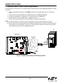
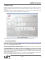
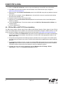
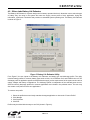
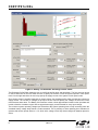
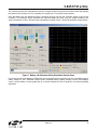
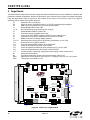
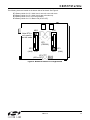
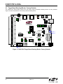
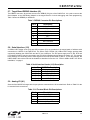
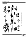
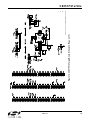
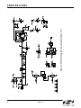
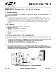
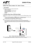
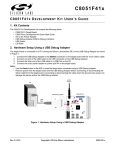
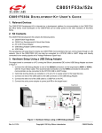
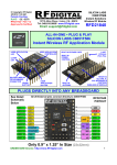
C8051F91x/90x C8051F912 D E V E L O P M E N T K I T U SER ’ S G UIDE 1. Relevant Devices The C8051F912 Development Kit is intended as a development platform for the microcontrollers in the C8051F91x-C8051F90x MCU family. The members of this MCU family are C8051F912, C8051F911, C8051F902, and C8051F901. Notes: 1. The target board included in this kit is provided with a pre-soldered C8051F912 MCU (QSOP24 package). 2. Code developed on the C8051F912 can be easily ported to the other members of this MCU family. 3. Refer to the C8051F91x-C8051F90x data sheet for the differences between the members of this MCU family. 2. Kit Contents The C8051F912 Development Kit contains the following items: C8051F912 Target Board Development Kit Quick-Start Guide AC to DC Power Adapter USB Debug Adapter (USB to Debug Interface) 2 USB Cables 2 AAA Batteries CD-ROM C8051Fxxx Figure 1. C8051F912 Target Board Rev. 0.2 2/14 Copyright © 2014 by Silicon Laboratories C8051F91x/90x C8051F91x/90x 3. Hardware Setup Using a USB Debug Adapter The target board is connected to a PC running the Silicon Laboratories IDE via the USB Debug Adapter as shown in Figure 2. 1. Connect the USB Debug Adapter to the DEBUG connector on the target board with the 10-pin ribbon cable. 2. Connect one end of the USB cable to the USB connector on the USB Debug Adapter. 3. Verify that a shorting block is installed on J17 and that SW5 is in the ON position. 4. Connect the other end of the USB cable to a USB Port on the PC. 5. Connect the ac/dc power adapter to power jack P2 on the target board (Optional). Notes: Use the Reset button in the IDE to reset the target when connected using a USB Debug Adapter. power from the target board and the USB Debug Adapter before connecting or disconnecting the ribbon cable from the target board. Connecting or disconnecting the cable when the devices have power can damage the device and/or the USB Debug Adapter. Remove PC Target Board P1.6 R15 P0.2 P0.3 USB Debug Adapter P1.5 J16 USB POWER P3 J15 TOUCH SENSE SWITCH P2.1 J8 +1VD J11 AAA_BAT WALL_PWR J13 J3 J14 +3VD RESET J6 VDD/DC+ J5 H1 IMEASURE ` J2 J17 H2 OFF ON SW5 VBAT POWER OFF BEFORE SWITCHING MODE J10 COIN_CELL J7 1 CELL U1 F912 J1 USB Cable AC/DC Adapter SW4 VBAT Power J9 J12 2 CELL www.silabs.com Run U3 SILICON LABS DEBUG J4 Silicon Laboratories USB DEBUG ADAPTER CP 2103 Stop TOUCH SENSE SWITCH P2.0 P2 Figure 2. Hardware Setup Using a USB Debug Adapter 2 Rev. 0.2 C8051F91x/90x 4. Software Setup Simplicity Studio greatly reduces development time and complexity with Silicon Labs EFM32 and 8051 MCU products by providing a high-powered IDE, tools for hardware configuration, and links to helpful resources, all in one place. Once Simplicity Studio is installed, the application itself can be used to install additional software and documentation components to aid in the development and evaluation process. Figure 3. Simplicity Studio The following Simplicity Studio components are required for the C8051F912 Development Kit: 8051 Products Part Support Simplicity Developer Platform Download and install Simplicity Studio from www.silabs.com/8bit-software or www.silabs.com/simplicity-studio. Once installed, run Simplicity Studio by selecting StartSilicon LabsSimplicity StudioSimplicity Studio from the start menu or clicking the Simplicity Studio shortcut on the desktop. Follow the instructions to install the software and click Simplicity IDE to launch the IDE. The first time the project creation wizard runs, the Setup Environment wizard will guide the user through the process of configuring the build tools and SDK selection. In the Part Selection step of the wizard, select from the list of installed parts only the parts to use during development. Choosing parts and families in this step affects the displayed or filtered parts in the later device selection menus. Choose the C8051F91x family by checking the C8051F91x/90x check box. Modify the part selection at any time by accessing the Part Management dialog from the WindowPreferencesSimplicity StudioPart Management menu item. Simplicity Studio can detect if certain toolchains are not activated. If the Licensing Helper is displayed after completing the Setup Environment wizard, follow the instructions to activate the toolchain. Rev. 0.2 3 C8051F91x/90x 4.1. Running Blinky Each project has its own source files, target configuration, SDK configuration, and build configurations such as the Debug and Release build configurations. The IDE can be used to manage multiple projects in a collection called a workspace. Workspace settings are applied globally to all projects within the workspace. This can include settings such as key bindings, window preferences, and code style and formatting options. Project actions, such as build and debug are context sensitive. For example, the user must select a project in the Project Explorer view in order to build that project. To create a project based on the Blinky example: 1. Click the Simplicity IDE tile from the Simplicity Studio home screen. 2. Click the Create new project link from the welcome screen or go to FileNewSilicon Labs MCU Project. 3. In the Kit drop-down, select C8051F912 Development Kit, in the Part drop-down, select C8051F912, and in the SDK drop-down, select the desired SDK. Click Next. 4. Select Example and click Next. 5. Under C8051F912 Development Kit in the Blinky folder, select F912-902 Blinky and click Finish. 6. Click on the project in the Project Explorer and click Build, the hammer icon in the top bar. Alternatively, go to ProjectBuild Project. 7. Click Debug to download the project to the hardware and start a debug session. 8. Press the Resume button to start the code running. The LED should blink. 9. Press the Suspend button to stop the code. 10. Press the Reset the device button to reset the target MCU. 11. Press the Disconnect button to return to the development perspective. 4.2. Simplicity Studio Help Simplicity Studio includes detailed help information and device documentation within the tool. The help contains descriptions for each dialog window. To view the documentation for a dialog, click the question mark icon in the window: This will open a pane specific to the dialog with additional details. The documentation within the tool can also be viewed by going to HelpHelp Contents or HelpSearch. 4 Rev. 0.2 C8051F91x/90x 4.3. Legacy 8-bit IDE Note: Using the Simplicity Studio tools with the C8051F912 Development Kit is recommended. See section 4. "Software Setup‚" on page 3 for more information. Download the 8-bit software from the website (www.silabs.com/8bit-software) or use the provided installer on the CD-ROM to install the software tools for the C8051F91x/90x devices. After installation, examples can be found in ...\Examples\C8051F91x_90x in the installation directory. At a minimum, the C8051F912 DK requires: Silicon Labs IDE—Software enabling initial evaluation, development, and debugging. Wizard 2—Initialization code generation software for the C8051F91x/90x devices. Keil C51 Tools—Keil 8051 Compiler/Assembler/Linker toolchain. CP210x Drivers—Virtual COM Port (VCP) drivers for the CP210x COM interface. More information on this installation process can be found in Section 4.4. Other software available includes: Configuration Keil µVision Driver—Driver for the Keil µVision IDE that enables development and debugging on C8051Fxxx MCUs. Flash Programming Utilities and MCU Production Programmer—Programming utilities for the production line. More information on the available programming options can be found on the website: http://www.silabs.com/products/mcu/Pages/ProgrammingOptions.aspx. ToolStick Development Tools—Software and examples for the ToolStick development platform. More information on this platform can be found at www.silabs.com/toolstick. Also available on the 8-bit software webpage is the Battery Life Estimator, which gives designers a quick and easy way to understand the discharge characteristics of different system configurations to help optimize low-power applications. The development kit includes the latest version of the C51 Keil 8051 toolset. This toolset is initially limited to a code size of 2 kB and programs start at code address 0x0800. After registration, the code size limit is removed entirely and programs will start at code address 0x0000. To register the Keil toolset: 1. Find the Product Serial Number printed on the CD-ROM. If you no longer have this serial number, register on the Silicon Labs website (www.silabs.com/8bit-software) to obtain the serial number. 2. Open the Keil µVision4 IDE from the installation directory with administrative privileges. 3. Select FileLicense Management to open the License Management window. Figure 4. Keil µVision4 IDE License Management Window Rev. 0.2 5 C8051F91x/90x 4. Click on the Get LIC via Internet... button to open the Obtaining a License IDE Code (LIC) window. 5. Press OK to open a browser window to the Keil website. If the window doesn’t open, navigate to www.keil.com/license/install.htm. 6. Enter the Silicon Labs Product Serial Number printed on the CD-ROM, along with any additional required information. 7. Once the form is complete, click the Submit button. An email will be sent to the provided email address with the license activation code. 8. Copy the License ID Code (LIC) from the email. 9. Paste the LIC into the New License ID Code (LIC) text box at the bottom of the License Management window in µVision4. 10. Press the Add LIC button. The window should now list the PK51 Prof. Developers Kit for Silabs as a licensed product. 11. Click the Close button. 4.4. CP210x USB to UART VCP Driver Installation The MCU Card includes a Silicon Labs CP210x USB-to-UART Bridge Controller. Device drivers for the CP210x need to be installed before the PC software can communicate with the MCU through the UART interface. Use the drivers included CD-ROM or download the latest drivers from the website (www.silabs.com/interface-software). 1. If using the CD-ROM, the CP210x Drivers option will launch the appropriate driver installer. If downloading the driver package from the website, unzip the files to a location and run the appropriate installer for the system (x86 or x64). 2. Accept the license agreement and follow the steps to install the driver on the system. The installer will let you know when your system is up to date. The driver files included in this installation have been certified by Microsoft. 3. To complete the installation process, connect the included USB cable between the host computer and the COM PORT USB connector (J5) on the MCU Card. Windows will automatically finish the driver installation. Information windows will pop up from the taskbar to show the installation progress. 4. If needed, the driver files can be uninstalled by selecting Windows Driver Package—Silicon Laboratories... option in the Programs and Features window. 6 Rev. 0.2 C8051F91x/90x 4.5. Silicon Labs Battery Life Estimator The Battery Life Estimator is a system design tool for battery operated devices. It allows the user to select the type of battery they are using in the system and enter the supply current profile of their application. Using this information, it performs a simulation and provides an estimated system operating time. The Battery Life Estimator is shown in Figure 5. Figure 5. Battery Life Estimator Utility From Figure 5, the two inputs to the Battery Life Estimator are battery type and discharge profile. The utility includes battery profiles for common battery types such as AAA, AA, A76 Button Cell, and CR2032 coin cell. The discharge profile is application-specific and describes the supply current requirements of the system under various supply voltages and battery configurations. The discharge profile is independent of the selected power source. Several read-only discharge profiles for common applications are included in the pulldown menu. The user may also create a new profile for their own applications. To create a new profile: 1. Select the profile that most closely matches the target application or choose the "Custom Profile". 2. Click Manage 3. Click Duplicate 4. Click Edit Profiles may be edited with the easy-to-use GUI (shown in Figure 6). Rev. 0.2 7 C8051F91x/90x Figure 6. Battery Life Estimator Discharge Profile Editor The Discharge Profile Editor allows the user to modify the profile name and description. The four text entry boxes on the left hand side of the form allow the user to specify the amount of time the system spends in each power mode. On the right hand side, the user may specify the supply current of the system in each power mode. Since supply current is typically dependent on supply voltage, the discharge profile editor provides two columns for supply current. The V2 and V1 voltages at the top of the two columns specify the voltages at which the current measurements were taken. The Battery Life Estimator creates a linear approximation based on the input data and is able to feed the simulation engine with an approximate supply current demand for every input voltage. The minimum system operating voltage input field allows the system operating time to stop increasing when the simulated battery voltage drops below a certain threshold. This is primarily to allow operating time estimates for systems that cannot operate down to 1.8 V, which is the voltage of two fully drained single-cell batteries placed in series. 8 Rev. 0.2 C8051F91x/90x The wakeup frequency box calculates the period of a single iteration through the four power modes and displays the system wake up frequency. This is typically the "sample rate" in low power analog sensors. Once the battery type and discharge profile is specified, the user can click the "Simulate" button to start a new simulation. The simulation engine calculates the estimated battery life when using one single-cell battery, two single-cell batteries in series, and two single-cell batteries in parallel. Figure 7 shows the simulation output window. Figure 7. Battery Life Estimator Utility Simulation Results Form The primary outputs of the Battery Life Estimator are an estimated system operating time and a simulated graph of battery voltage vs. time. Additional outputs include estimated battery capacity, average current, self-discharge current, and the ability to export graph data to a comma delimited text file for plotting in an external graphing application. Rev. 0.2 9 C8051F91x/90x 5. Target Board The C8051F912 Development Kit includes a target board with a C8051F912 device pre-installed for evaluation and preliminary software development. Numerous input/output (I/O) connections are provided to facilitate prototyping using the target board. Refer to Figure 8 for the locations of the various I/O connectors. Figure 10 on page 12 shows the factory default shorting block positions. P1 P2 P3 J1 J2, J3 J5 J6 J7 J8 J9 J10, J11 J12 J13 J14 J15 J16 J17 H1 H2 SW4 SW5 Expansion connector (96-pin) Power connector (accepts input from 7 to 15 VDC unregulated power adapter) USB connector (connects to PC for serial communication) Enable/Disable VBAT Power LED Port I/O headers (provide access to Port I/O pins) Enable/Disable VDD/DC+ Power LED Provides an easily accessible ground clip Connects pin P0.7 (IREF0 Output) to resistor R14 and capacitor C19 Connects P0.2 and P0.3 to switches and P1.5 and P1.6 to LEDs DEBUG connector for Debug Adapter interface Selects the power supply source (Wall Power, AAA Battery, or Coin Cell) Connects Port I/O to UART0 interface Connects external VREF capacitor to the P0.0/VREF Connects the PCB ground plane to P0.1/AGND Connects negative potentiometer (R14) terminal to pin P1.4 or to GND Connects the potentiometer (R14) wiper to P0.6/CNVSTR Creates an open in the power supply path to allow supply current measurement Analog I/O terminal block Provides terminal block access to the input and output nodes of J17 Switches the device between one-cell (0.9–1.8 V supply) or two-cell (1.8–3.6 V) mode Turns power to the MCU on or off P1.6 R15 J16 P1.4 J15 GND P0.2 P1.5 SW2 P0.3 SW3 USB POWER P3 TOUCH SENSE SWITCH P1.0 TOUCH SENSE SWITCH P1.1 CP 2103 U3 SILICON LABS J9 J12 DEBUG J8 +1VD J11 P1 AAA_BAT WALL_PWR J13 SW1 J14 J3 +3VD RESET J6 VDD/DC+ J5 IMEASURE PORT0 ` J2 J17 H2 OFF ON H1 SW5 Figure 8. C8051F912 Target Board Rev. 0.2 SW4 VBAT Pin 1 10 VBAT POWER OFF BEFORE SWITCHING MODE J7 PORT1 J10 COIN_CELL 1 CELL U1 F912 2 CELL www.silabs.com J1 P2 Pin 1 Pin 2 C8051F91x/90x The following items are located on the bottom side of the board. See Figure 9. BT1 Battery Holder for 1.5 V AAA. Use for one-cell or two-cell mode. BT2 Battery Holder for 1.5 V AAA. Use for two-cell mode only. BT3 Battery Holder for 3 V Coin Cell (CR2032). BT4 Battery Holder for 1.5 V Button Cell (A76 or 357). NEG POS Note: BT2 is only used in two-cell mode. BT3 (CR2032) BT2 BT1 (AAA) POS NEG (AAA) BT4 (A76 or 357) Figure 9. Bottom of C8051F912 Target Board Rev. 0.2 11 C8051F91x/90x 5.1. Target Board Shorting Blocks: Factory Defaults The C8051F912 Target Board comes from the factory with pre-installed shorting blocks on many headers. Figure 10 shows the positions of the factory default shorting blocks. P1.6 R15 USB POWER P3 TOUCH SENSE SWITCH P1.0 TOUCH SENSE SWITCH P1.1 CP 2103 U3 SILICON LABS J8 J9 J12 +1VD U1 F912 J11 P1 J13 AAA_BAT WALL_PWR SW1 J14 +3VD J7 PORT1 J3 RESET J6 VDD/DC+ J5 PORT0 IMEASURE ` J2 J17 H2 OFF ON H1 SW5 VBAT POWER OFF BEFORE SWITCHING MODE J10 COIN_CELL 1 CELL www.silabs.com 2 CELL P1.4 J15 GND P0.3 SW3 DEBUG J16 P0.2 P1.5 SW2 SW4 VBAT J1 P2 Pin 1 Figure 10. C8051F912 Target Board Shorting Blocks: Factory Defaults 12 Rev. 0.2 Pin 1 Pin 2 C8051F91x/90x 5.2. Target Board Power Options and Current Measurement (J10, J11, J17, H2, P2, P3, SW4, SW5) The C8051F912 Target Board supports three power options, selectable by the three-way header (J10/J11). The power options vary based on the configuration (one-cell or two-cell mode) selected by SW4. Power to the MCU may be switched on/off using the power switch (SW5). Important Note: The power switch (SW5) must be in the OFF position prior to switching between one-cell and two-cell mode using SW4. The power options are described in the paragraphs below. 5.2.1. Wall Power When the J10/J11 three-way header is set to WALL_PWR, the C8051F912 Target Board may be powered from the following power sources: 9 VDC power using the ac to dc power adapter (P2) VDC USB VBUS power from PC via the USB Debug Adapter (J9) 5 VDC USB VBUS power from PC via the CP2103 USB connector (P3) 5 All the three power sources are ORed together using reverse-biased diodes (D1, D2, D3), eliminating the need for headers to choose between the sources. The target board will operate as long as any one of the power sources is present. The ORed power is regulated to a 3.3 V dc voltage using a LDO regulator (U2). The output of the regulator powers the +3 VD net on the target board. If SW4 is configured to select two-cell mode, the VBAT supply net on the target board is powered directly from the +3 VD net. If SW4 is configured to select one-cell mode, the VBAT supply net is powered directly from the +1 VD. This power supply net takes +3 VD and passes it through a 1.65 V LDO. The LDO’s output voltage is variable and can be set by changing the value of resistor R32. J11 J10 COIN_CELL VBAT AAA_BAT WALL_PWR 5.2.2. AAA Battery When the J10/J11 three-way header is set to AAA_BAT, the C8051F912 Target Board may be powered from a single AAA battery inserted in BT1 or from the series combination of the AAA batteries inserted in BT1 and BT2. A single battery is selected when SW4 is configured to one-cell mode. The two AAA batteries configured in series to provide a voltage of ~3 V are selected when SW4 is configured to two-cell mode. J11 J10 COIN_CELL VBAT AAA_BAT WALL_PWR 5.2.3. Coin Cell Battery When the J10/J11 three-way header is set to COIN_CELL, the C8051F912 Target Board may be powered from a single 1.5 V Alkaline (A76) or Silver Oxide (357) button cell inserted in BT4 or from a single 3 V Lithium (CR2032) coin cell inserted in BT3. The button cell (BT4) is selected when SW4 is configured to one-cell mode, and the coin cell (BT3) is selected when SW4 is configured to two-cell mode. J11 J10 COIN_CELL AAA_BAT WALL_PWR VBAT 5.2.4. Measuring Current The header (J17) and terminal block (H2) provide a way to measure the total supply current flowing from the power supply source to the MCU. The measured current does not include any current from the VBAT LED (DS2), the address latch (U4) or the quiescent current from the power supply; however, it does include the current used by any LEDs powered from the VDD/DC+ supply net or sourced through a GPIO pin. See the target board schematic Rev. 0.2 13 C8051F91x/90x in Figure 11 through Figure 13 for additional information. 5.3. System Clock Sources 5.3.1. Internal Oscillators The C8051F912 device installed on the target board features a factory calibrated programmable high-frequency internal oscillator (24.5 MHz base frequency, ±2%) and a low power internal oscillator (20 MHz ±10%). After each reset, the low power oscillator divided by 8 results in a default system clock frequency of 2.5 MHz (±10%). The selected system clock and the system clock divider may be configured by software for operation at other frequencies. For low-frequency operation, the C8051F912 features a smaRTClock real time clock. A 32.768 kHz Watch crystal (Y2) is included on the target board. If you wish to operate the C8051F912 device at a frequency not available with the internal oscillators, an external crystal may be used. Refer to the C8051F91x-C8051F90x data sheet for more information on configuring the system clock source. 5.3.2. External Oscillator Options The target board is designed to facilitate the installation of an external crystal (Y1). Install a 10 M resistor at R9 and install capacitors at C20 and C21 using values appropriate for the crystal you select. If you wish to operate the external oscillator in capacitor or RC mode, options to install a capacitor or an RC network are also available on the target board. Populate C21 for capacitor mode, and populate R16 and C21 for RC mode. Refer to the C8051F91xC8051F90x data sheet for more information on the use of external oscillators. 5.4. Port I/O Headers (J2, J3, J6) Access to all Port I/O on the C8051F912 is provided through the headers J2 and J3. The header J6 provides access to the ground plane for easy clipping of oscilloscope probes. 14 Rev. 0.2 C8051F91x/90x 5.5. Switches and LEDs (J1, J5, J8, J15, J16) Three push-button switches are provided on the target board. Switch SW1 (RESET) is connected to the reset pin of the C8051F912. Pressing SW1 puts the device into its hardware-reset state. Switches SW2 (P0.2) and SW3 (P0.3) are connected to the C8051F912’s general purpose I/O (GPIO) pins through headers. Pressing SW2 or SW3 generates a logic low signal on the port pin. Remove the shorting block from the header (J8) to disconnect the switches from the port pins. The port pin signal is also routed to pins on the J2 and P1 I/O connectors. See Table 1 for the port pins and headers corresponding to each switch. Two touch sensitive (contactless) switches are provided on the target board. The operation of these switches require appropriate firmware running on the C8051F912 MCU that can sense the state of the switch. Five power LEDs are provided on the target board to serve as indicators. Each of the two regulators has a red LED used to indicate the presence of power at the output of the regulator. A red USB Power LED turns on when a USB cable is plugged into the USB connector P3. One power LED is also added to each of the two primary supply nets powering the MCU (VDD/DC+ and VBAT). The LEDs connected to the supply nets may be disabled by removing the shorting blocks from J1 and J5. Two LEDs are connected to GPIO pins P1.5 and P1.6 for use by application software. See Table 1 for the port pins and headers corresponding to each LED. A potentiometer (R15) is also provided on the target board for generating analog signals. Place a shorting block on J16 to connect the wiper to P0.6/CNVSTR. The header J15 allows the negative terminal of the potentiometer to be tied to GND or to P1.4. When tied to GND, the potentiometer is always enabled and will draw a measurable amount of supply current. When tied to P1.4, it only draws current when P1.4 is driving a logic 0 and draws no current when P1.4 is driving a logic 1. Table 1. Target Board I/O Descriptions Description I/O Header(s) SW1 SW2 SW3 P1.0 (Touch Sense Switch) P1.1 (Touch Sense Switch) Red LED (P1.5) Yellow LED (P1.6) Red LED (VDD/DC+) Red LED (VBAT) Red LED (USB Power) Red LED (+1 VD Power) Red LED (+3 VD Power) Potentiometer (R15) Reset P0.2 P0.3 P1.0 P1.1 P1.5 P1.6 VDD/DC+ Supply Net VBAT Supply Net USB VBUS +1 VD Regulator Output +3 VD Regulator Output P0.6/P1.4 none J8[5–6] J8[7–8] none none J8[1–2] J8[3–4] J5 J1 none none none J15, J16 Rev. 0.2 15 C8051F91x/90x 5.6. Expansion I/O Connector (P1) The 96-pin Expansion I/O connector P1 provides access to all signal pins of the C8051F912 device (except the C2 debug interface signals). In addition, power supply and ground pins are included. A small through-hole prototyping area is also provided. See Table 2 for a list of pin descriptions for P1. Table 2. P1 Pin Descriptions 16 Row A Pin # Description Row B Pin # Description Row C Pin # Description 1 +3 VD 1 GND 1 nc 2 nc 2 nc 2 nc 3 nc 3 nc 3 nc 4 nc 4 nc 4 nc 5 nc 5 nc 5 nc 6 nc 6 nc 6 nc 7 nc 7 nc 7 nc 8 nc 8 nc 8 nc 9 nc 9 nc 9 nc 10 nc 10 P0.7/IREF0 10 P0.6/CNVSTR 11 P0.5/RX 11 P0.4/TX 11 P0.3H 12 P0.2H 12 P0.1/AGND 12 P0.0/VREF 13 P2.7H 13 P1.6 13 P1.5 14 P1.4 14 P1.3 14 P1.2 15 P1.1 15 P1.0 15 nc 16 nc 16 nc 16 nc 17 nc 17 nc 17 nc 18 nc 18 nc 18 nc 19 nc 19 nc 19 nc 20 nc 20 nc 20 nc 21 nc 21 nc 21 nc 22 nc 22 nc 22 nc 23 nc 23 nc 23 nc 24 nc 24 nc 24 nc 25 nc 25 GND 25 nc 26 GND 26 nc 26 nc 27 nc 27 nc 27 nc 28 nc 28 VDD/DC+ 28 VBAT 29 nc 29 nc 29 nc 30 nc 30 nc 30 nc 31 nc 31 nc 31 nc 32 nc 32 GND 32 nc Rev. 0.2 C8051F91x/90x 5.7. Target Board DEBUG Interface (J9) The DEBUG connector J9 provides access to the DEBUG (C2) pins of the C8051F912. It is used to connect the Serial Adapter or the USB Debug Adapter to the target board for in-circuit debugging and Flash programming. Table 3 shows the DEBUG pin definitions. Table 3. DEBUG Connector Pin Descriptions Pin # Description 1 +3 VD (+3.3 VDC) 2, 3, 9 GND (Ground) 4 P2.7/C2D 5 RST (Reset) 6 P2.7 7 RST/C2CK 8 Not Connected 10 USB Power (+5 VDC from J9) 5.8. Serial Interface (J12) A USB-to-UART bridge circuit (U3) and USB connector (P3) are provided on the target board to facilitate serial connections to UART0 of the C8051F912. The Silicon Labs CP2103 (U3) USB-to-UART bridge provides data connectivity between the C8051F912 and the PC via a USB port. The VIO power supply and TX, RX, RTS and CTS signals of UART0 may be connected to the CP2103 by installing shorting blocks on header J12. The shorting block positions for connecting each of these signals to the CP2103 are listed in Table 4. To use this interface, the USB-to-UART device drivers should be installed as described in Section 4.4. "CP210x USB to UART VCP Driver Installation‚" on page 6. Table 4. Serial Interface Header (J12) Description Header Pins UART0 Pin Description J12[9–10] J12[7–8] J12[5–6] J12[3–4] J12[1–2] CP2103_VIO (VDD/DC+) TX_MCU (P0.5) RX_MCU (P0.4) RTS (P0.6) CTS (P0.7) 5.9. Analog I/O (H1) Several of the C8051F912 target device’s port pins are connected to the H1 terminal block. Refer to Table 5 for the H1 terminal block connections. Table 5. H1 Terminal Block Pin Descriptions Pin # Description 1 2 3 4 P0.6/CNVSTR P0.7/IREF0 GND (Ground) P0.0/VREF (Voltage Reference) Rev. 0.2 17 C8051F91x/90x 5.10. IREF Connector (J7) The C8051F912 Target Board also features a current-to-voltage 1 k load resistor that may be connected to the current reference (IREF0) output that can be enabled on port pin (P0.7). Install a shorting block on J7 to connect port pin P0.7 of the target device to the load resistor. If enabled by software, the IREF0 signal is then routed to the J2[8] and H1[2] connectors. 5.11. VREF and AGND Connector (J13, J14) The C8051F912 Target Board also features 4.7 µF capacitor in parallel with a 0.1 µF that can be connected to P0.0/VREF when using the Precision Voltage Reference. The capacitors are connected to P0.0/VREF when a shorting block is installed on J13. Using the Precision Voltage Reference is optional since 'F91x-'F90x devices have an on-chip High-Speed Voltage Reference. The shorting block J14 allows P0.1/AGND to be connected to ground. This provides a noise-free ground reference to the analog-to-digital Converter. The use of this dedicated analog ground is optional. 5.12. C2 Pin Sharing On the C8051F912, the debug pins C2CK and C2D are shared with the pins RST and P2.7, respectively. The target board includes the resistors necessary to enable pin sharing which allow the RST and P2.7 pins to be used normally while simultaneously debugging the device. See Application Note “AN124: Pin Sharing Techniques for the C2 Interface” at www.silabs.com for more information regarding pin sharing. 18 Rev. 0.2 C8051F91x/90x 6. Frequently Asked Questions 1. Should power be turned off when switching between one-cell and two-cell mode? Yes, power must be turned off by placing SW5 in the OFF position when switching between one-cell and two-cell mode. Switching between modes while power is on may result in increased power consumption and possible damage to low voltage transistors. 2. I have placed the MCU in Sleep Mode. Why is the supply current greater than 1 µA? This can be caused by a number of factors. Check the following: a. Verify that the USB Debug Adapter is not connected to the device. When connected, it can draw approximately 2–5 µA from the VDD/DC+ supply net. b. Verify that the P1.5 and P1.6 LEDs are turned off in software (P1.5 and P1.6 set to logic HIGH). Alternatively, the P1.5 and P1.6 LEDs can be disabled by removing the corresponding shorting blocks from J8. c. Verify that the VDD/DC+ Power LED is disabled (remove shorting block from J5). d. Verify that the shorting block on J15 does not connect the potentiometer negative terminal to GND, since this would result in continuous current of ~ 300 µA. The shorting block may be removed, or configured to enable the potentiometer when P1.4 is set to logic LOW. When the potentiometer enable is under software control, be sure to set P1.4 to logic HIGH prior to placing the device in Sleep Mode. e. Verify that J7, J13, and J14 do not have shorting blocks installed. 3. I have been measuring the sleep mode current using the “µA” setting on my multimeter. Why am I no longer able to connect to the IDE? When most multimeters are placed in “µA” mode, a large resistance is placed in series with the power supply. This “current limiting” resistor prevents the MCU from starting up. To measure current during startup, make sure that the multimeter is configured to its “mA” setting. Alternatively, a shorting block can be placed on J17 to ensure that the multimeter does not limit current during startup. 4. Where can I find a schematic of the C8051F912 Target Board? A target board schematic can be found in the C8051F912-DK User’s Guide which is available on the Development Tools CD and is installed in the following folder (by default): C:\SiLabs\MCU\Documentation\UsersGuides 5. Which power LED should I use to determine if the MCU is powered? The VDD/DC+ LED (DS5) should be used to determine if the MCU is powered. If you have applied power to the board, but the VDD/DC+ LED is not turning on, check the following: a. Verify that the correct power source (J10, J11) is selected. b. Verify that J17 has a shorting block. c. Verify that SW5 is in the ON position. d. Verify that J5 has a shorting block installed. Rev. 0.2 19 C8051F91x/90x 6. What can I do to reduce active supply current? Below are some suggestions for reducing the active supply current: a. Clear all wake-up sources in the PCU0CF register. This will allow the low power oscillator to be disabled when it is not being used as the system clock. This optimization can reduce the supply current by up to 30 µA. b. When operating at system clock frequencies above 10 MHz, minimize supply current by setting the BYPASS bit (FLSCL.6) to 1. If the system clock needs to decrease below 10 MHz, clear the BYPASS bit to 0. c. If the precision oscillator is not being used, turn off the precision oscillator bias by setting the OSCBIAS bit (REG0CN.4) to 0. 7. Why does P0.7/IREF0 have a voltage of 200 mV when IREF0CN is set to 0x00? When IREF0CN is set to 0x00, the current reference is completely turned off. When a shorting block is installed on J7, the voltage at P0.7/IREF0 should be 0 V unless one of the following conditions is present: a. The P0.7/IREF0 pin is not configured for analog I/O (weak pull-up enabled). b. The P0.7/IREF0 pin is being used as CTS (a shorting block is installed on J12). 8. I have configured a Port pin as an analog input. Why is it still shorted to ground? On C8051F91x-C8051F90x devices, configuring a Port pin to analog mode (using PnMDIN) disables the digital input path and the weak pull-up. It does not explicitly disable the output drivers. Software can ensure that the output drivers are disabled by configuring the Port pin to open-drain output mode (using PnMDOUT) and writing 1 to the port latch. 9. Why does power consumption increase when an analog signal (hovering around mid-supply) is connected to a digital input? This phenomenon is called the “crowbar” effect and is present in all CMOS circuitry. If the input of a CMOS structure is not a strong 1 or 0, then both the PMOS and NMOS devices are partially turned on causing current flow from VDD to GND. To prevent the “crowbar” effect, ensure that pins with analog voltage levels are configured for analog I/O. 10. Why does the dc/dc converter stop regulating when the load current exceeds 10 mA? The default register settings for the dc/dc converter are optimized for low power applications requiring less than 10 mA of supply current. If the application requires additional supply current, the default values may be overridden to provide up to 65 mW of output power. To configure the dc/dc converter to high power mode, perform the following steps prior to enabling any high power device: a. Set DC0CN = 0x01. This selects the high-current switches. b. Set DC0CF = 0x04. This sets the peak inductor current limit to 500 mA. 20 Rev. 0.2 C8051F91x/90x 11. When the missing clock detector is enabled, why does the MCU reset if I switch from the default system clock (Low Power Oscillator divided by 8) to smaRTClock divided by 1? Background: —The missing clock detector will trigger a reset if the system clock period exceeds 100 µs. —Switchover between clock sources occurs in 1 clock cycle of the slowest clock. —Changing the clock divide value requires up to 128 cycles of the undivided clock source. Since the clock source change occurs in a single cycle and the clock divide change can take up to 128 cycles, the system clock will be set to the new clock source divided by the old divide value for a brief period of time. In this example, the actual system clock will be 4.096 kHz for up to 128 cycles of the undivided clock source. This causes the missing clock detector to time out and reset the MCU. The proper way of changing the system clock when both the clock source and the clock divide value are being changed is as follows: If switching from a fast “undivided” clock to a slower “undivided” clock: a. Change the clock divide value. b. Poll for CLKRDY > 1. c. Change the clock source. If switching from a fast “undivided” clock to a slower “undivided” clock: d. Change the clock source. e. Change the clock divide value. f. Poll for CLKRDY > 1. 12. Why is the MCU pre-maturely released from reset when using a wall supply with a slow rise time? The maximum VDD Ramp Time is specified at 3 ms. If the power supply ramp takes longer than 3 ms to reach 0.9 V, then the device may be released from reset before the supply has reached the minimum operating voltage. The slow ramp time (>3 ms) can occur when using a bench power supply that does not have an output enable switch. Rev. 0.2 21 Figure 11. C8051F912 Target Board Schematic (Page 1 of 3) C8051F91x/90x 7. Schematics 22 Rev. 0.2 Figure 12. C8051F912 Target Board Schematic (Page 2 of 3) C8051F91x/90x Rev. 0.2 23 Figure 13. C8051F912 Target Board Schematic (Page 3 of 3) C8051F91x/90x 24 Rev. 0.2 C8051F91x/90x CONTACT INFORMATION Silicon Laboratories Inc. 400 West Cesar Chavez Austin, TX 78701 Please visit the Silicon Labs Technical Support web page: http://www.silabs.com/support and register to submit a technical support request. Patent Notice Silicon Labs invests in research and development to help our customers differentiate in the market with innovative low-power, small size, analogintensive mixed-signal solutions. Silicon Labs' extensive patent portfolio is a testament to our unique approach and world-class engineering team. The information in this document is believed to be accurate in all respects at the time of publication but is subject to change without notice. Silicon Laboratories assumes no responsibility for errors and omissions, and disclaims responsibility for any consequences resulting from the use of information included herein. Additionally, Silicon Laboratories assumes no responsibility for the functioning of undescribed features or parameters. Silicon Laboratories reserves the right to make changes without further notice. Silicon Laboratories makes no warranty, representation or guarantee regarding the suitability of its products for any particular purpose, nor does Silicon Laboratories assume any liability arising out of the application or use of any product or circuit, and specifically disclaims any and all liability, including without limitation consequential or incidental damages. Silicon Laboratories products are not designed, intended, or authorized for use in applications intended to support or sustain life, or for any other application in which the failure of the Silicon Laboratories product could create a situation where personal injury or death may occur. Should Buyer purchase or use Silicon Laboratories products for any such unintended or unauthorized application, Buyer shall indemnify and hold Silicon Laboratories harmless against all claims and damages. Silicon Laboratories and Silicon Labs are trademarks of Silicon Laboratories Inc. Other products or brandnames mentioned herein are trademarks or registered trademarks of their respective holders. Rev. 0.2 25