1
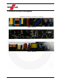
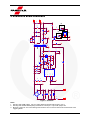
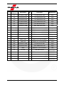
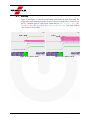
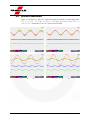
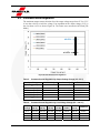
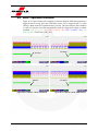
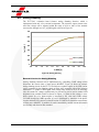
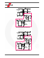
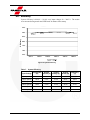
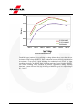
User Guide for FEBFL7733A_L51U030A High PF, Low THD, Wide Input Voltage Range Flyback LED Driver with Analog Dimming Function for 30 W LED Lamp Featured Fairchild Product: FL7733A Direct questions or comments about this evaluation board to: “Worldwide Direct Support” Fairchild Semiconductor.com © 2014 Fairchild Semiconductor Corporation 1 FEBFL7733A_L51U030A • Rev. 1.0.0 Table of Contents 1. Introduction ............................................................................................................................. 3 1.1. General Description of FL7733A .................................................................................... 3 1.2. Controller Features........................................................................................................... 3 1.3. Controller Internal Block Diagram .................................................................................. 4 2. Evaluation Board Specifications ............................................................................................. 5 3. Evaluation Board Photographs ................................................................................................ 6 4. Evaluation Board Printed Circuit Board (PCB) ...................................................................... 7 5. Evaluation Board Schematic ................................................................................................... 8 6. Evaluation Board Bill of Materials ......................................................................................... 9 7. Transformer Design ............................................................................................................... 11 8. Evaluation Board Performance ............................................................................................. 12 8.1. Startup ............................................................................................................................ 13 8.2. Operation Waveforms .................................................................................................... 14 8.3. Constant-Current Regulation ......................................................................................... 16 8.4. Short- / Open-LED Protections ...................................................................................... 17 8.5. Analog Dimming ........................................................................................................... 19 8.6. Efficiency ....................................................................................................................... 21 8.7. Power Factor (PF) & Total Harmonic Distortion (THD) .............................................. 23 8.8. Harmonics ...................................................................................................................... 24 8.9. Operating Temperature .................................................................................................. 26 8.10. Electromagnetic Interference (EMI) ......................................................................... 27 9. Revision History .................................................................................................................... 28 © 2014 Fairchild Semiconductor Corporation 2 FEBFL7733A_L51U030A • Rev. 1.0.0 This user guide supports the evaluation kit for the FL7733A. It should be used in conjunction with the FL7733A datasheet as well as Fairchild’s application notes and technical support team. Please visit Fairchild’s website at www.fairchildsemi.com. 1. Introduction This document describes LED driver designed with flyback converter using the FL7733A Primary-Side Regulation (PSR) single-stage controller. The input voltage range is 90 VRMS ~ 300 VRMS and there is one DC output with a constant current of 0.58 A at 52 V. This document contains a general description of the FL7733A, the power supply solution specification, schematic, bill of materials, and typical operating characteristics with analog dimming function. 1.1. General Description of FL7733A The FL7733A is an active Power Factor Correction (PFC) controller for use in singlestage flyback topology or buck-boost topology. Primary-side regulation and single-stage topology minimize cost by reducing external components such as the input bulk capacitor and secondary side feedback circuitry. To improve power factor and Total Harmonic Distortion (THD), constant on-time control is utilized with an internal error amplifier and a low bandwidth compensator. Precise constant-current control provides accurate output current, independent of input voltage and output voltage. Operating frequency is proportionally changed by the output voltage to guarantee Discontinuous Current Mode (DCM) operation, resulting in high efficiency and simple designs. The FL7733A also provides open-LED, short-LED, and over-temperature protection functions. 1.2. Controller Features High Performance < ±3% Total Constant Current Tolerance Over All Conditions < ±1% Over Universal Line Voltage Variation < ±1% from 50% to 100% Load Voltage Variation < ±1% with ±20% Magnetizing Inductance Variation Primary-Side Regulation (PSR) Control for Cost-Effective Solution without Requiring Input Bulk Capacitor and Secondary Feedback Circuitry Application Input Voltage Range: 80 VAC - 308 VAC High PF and Low THD Over Universal Line Input Range Fast < 200 ms Startup (at 90 VAC) using Internal High-Voltage Startup with VDD Regulation Adaptive Feedback Loop Control for Startup without Overshoot High Reliability LED Short / Open Protection Output Diode Short Protection Sensing Resistor Short / Open Protection VDD Over-Voltage Protection (OVP) VDD Under-Voltage Lockout (UVLO) Over-Temperature Protection (OTP) All Protections by Auto Restart Cycle-by-Cycle Current Limit Application Voltage Range: 80 VAC ~ 308 VAC © 2014 Fairchild Semiconductor Corporation 3 FEBFL7733A_L51U030A • Rev. 1.0.0 1.3. Controller Internal Block Diagram Figure 1. Block Diagram of the FL7733A © 2014 Fairchild Semiconductor Corporation 4 FEBFL7733A_L51U030A • Rev. 1.0.0 2. Evaluation Board Specifications Table 1. Specifications for LED Lighting Load Symbol Value Comments VIN.MIN 90 VAC Minimum AC Line Input Voltage VIN.MAX 305 VAC Maximum AC Line Input Voltage VIN.NOMINAL 120 V / 230 V Nominal AC Line Input Voltage fIN 60 Hz / 50 Hz AC Line Frequency VOUT.MIN 25 V Minimum Output Voltage VOUT.MAX 55 V Maximum Output Voltage VOUT.NOMINAL 52 V Nominal Output Voltage IOUT.NOMINAL 0.58 A Nominal Output Current Max. CC Tolerance < ±0.43% Line Input Voltage Change: 90~300 VAC < ±0.61% Output Voltage Change: 25~55 V Eff90 VAC 89.46% Efficiency at 90 VAC Input Voltage Eff120 VAC 90.44% Efficiency at 120 VAC Input Voltage Eff140 VAC 90.75% Efficiency at 140 VAC Input Voltage Eff180 VAC 91.01% Efficiency at 180 VAC Input Voltage Eff230 VAC 90.88% Efficiency at 230 VAC Input Voltage Eff300 VAC 90.27% Efficiency at 300 VAC Input Voltage PF /THD90VAC 0.995 / 5.12% PF/THD at 90 VAC Input Voltage PF / THD120VAC 0.992 / 2.32% PF/THD at 120 VAC Input Voltage PF / THD140VAC 0.987 / 2.12% PF/THD at 140 VAC Input Voltage PF / THD180VAC 0.976 / 2.58% PF/THD at 180 VAC Input Voltage PF / THD230VAC 0.946 / 3.41% PF/THD at 230 VAC Input Voltage PF / THD300VAC 0.874 / 5.93% PF/THD at 300 VAC Input Voltage FL7733A TFL7733A 65.0ºC FL7733A Temperature MOSFET TMOSFET 75.4ºC Main MOSFET Temperature Rectifier TRectifier 76.0ºC Secondary Diode Temperature Transformer TTRANS 67.2ºC Transformer Temperature Description Voltage Input Frequency Voltage Output Current Efficiency PF / THD Max. Temperature Open-Frame (TA = 25ºC) All data of the evaluation board measured with the board was enclosed in a case and external temperature around TA=25°C. © 2014 Fairchild Semiconductor Corporation 5 FEBFL7733A_L51U030A • Rev. 1.0.0 3. Evaluation Board Photographs Dimensions: 155 mm (L) x 28 mm (W) x 25 mm (H) Figure 2. Top View Figure 3. Bottom View Figure 4. Side View © 2014 Fairchild Semiconductor Corporation 6 FEBFL7733A_L51U030A • Rev. 1.0.0 4. Evaluation Board Printed Circuit Board (PCB) Unit: mm Figure 5. Top Pattern Figure 6. Bottom Pattern © 2014 Fairchild Semiconductor Corporation 7 FEBFL7733A_L51U030A • Rev. 1.0.0 Ro1 50V GND 5. Evaluation Board Schematic R21 VDIMC8 1 (1) R10 R13 C11 5 VS 1 CS 2 GND 3 6 NC 7 HV N F1 MOV1 CF1 LF1 2 1 4 BD1 CF2 3 L C1 C6 R3 8 COMI U1 GATE VDD 4 VDD C3 R12 D1 C2 R4 R5 R6 R2 R1 D5 R11 C4 R8 D2 R9 C5 Q1 R7 R14 R15 C9 RM10 12P C7 D3 Do1 R18 T1 R17 U2 4 3 Co1 1 2 C10 R19 R22 (3) Con3 2 VDIM+ Q2 Co2 ZD1 R24 R25 R20 (2) Figure 7. Schematic Notes: 1. Dimming with A-DIM voltage: 0 to 10 V analog dimming signal should be input to Con 3. 2. Dimming with Variable Resistor [R21]: Please short Con 3's pin 1 to pin 2 with jumper wire. 3. Minimum current set: The current setting must be above 10% of nominal current level of this board to avoid triggering SRSP. © 2014 Fairchild Semiconductor Corporation 8 FEBFL7733A_L51U030A • Rev. 1.0.0 6. Evaluation Board Bill of Materials Item No. Part Reference Part Number Qty. Description Manufacturer 1 BD1 GBJ206 1 2 A / 600 V, Bridge Diode KD 2 CF1 B32922D3334K 1 330 nF / 310 VAC, X-Capacitor Carli 3 CF2 B32922C3104K 1 100 nF / 310 VAC, X-Capacitor Carli 4 Co1, Co2 KMG 470 μF / 63 V 2 470 μF / 63 V, Electrolytic Capacitor Smayoung 5 C1 MPE 630 V 154K 1 150 nF / 630 V, MPE Film Capacitor Sungho 6 C2 C1206C103KDRACTU 1 10 nF / 630 V, SMD Capacitor 1206 Kemet 7 C3 KMG 10 μF / 35 V 1 10 μF / 35 V, Electrolytic Capacitor Smayoung 8 C4 C0805C104K5RACTU 1 100 nF / 50 V, SMD Capacitor 2012 Kemet 9 C5 C0805C519C3GACTU 1 5.1 pF / 25 V, SMD Capacitor 2012 Kemet 10 C6 C0805C225K4RACTU 1 2.2 μF / 16 V, SMD Capacitor 2012 Kemet 11 C7 KMG 10 μF / 50 V 1 10 μF / 50 V, Electrolytic Capacitor Smayoung 12 C8 SCFz2E472M10BW 1 4.7 nF / 250 V, Y-Capacitor Samwha 13 C9 C0805C102K5RACTU 1 1.0 nF / 25 V, SMD Capacitor 2012 Kemet 14 C10 NC 15 C11 C0805C101K5GALTU 1 100 pF / 50 V, SMD Capacitor 2012 Kemet 16 Do1 ES3J 1 600 V/3 A, Fast Rectifier 17 D1 RS1M 1 1000 V/1 A, Ultra-Fast Recovery Diode 18 D2, D3 1N4003 2 200 V/1 A, General Purpose Rectifier 19 D5 LL4148 1 Small Signal Diode 20 U2 FOD817A 1 OPTOCOUPLER 4-Pin 21 F1 SS-5-2A 1 250 V / 2 A, Fuse Bussmann 22 LF1 B82733F 1 40 mH Common Inductor EPCOS 23 MOV1 SVC561D-10A 1 Metal Oxide Varistor Samwha 24 Q1 FCPF850N80Z 1 800 V / 850 mΩ, N-Channel MOSFET 25 Q2 MMBT2222AT 1 NPN General Purpose Amplifier 26 Ro1 RC1206JR-0747KL 1 47 kΩ, SMD Resistor 1206 Yageo 27 R1, R2, R3, R8 RC1206JR-0710KL 4 10 kΩ, SMD Resistor 1206 Yageo 29 R4, R5, R6 RC1206JR-07100KL 3 100 kΩ, SMD Resistor 1206 Yageo © 2014 Fairchild Semiconductor Corporation 9 Fairchild Semiconductor Fairchild Semiconductor Fairchild Semiconductor Fairchild Semiconductor Fairchild Semiconductor Fairchild Semiconductor Fairchild Semiconductor FEBFL7733A_L51U030A • Rev. 1.0.0 Item No. Part Reference Part Number Qty. Description Manufacturer 30 R7 RC1206JR-0710R0L 1 0 Ω, SMD Resistor 1206 Yageo 31 R9 RC1206JR-071R5L 1 1.5 Ω, SMD Resistor 1206 Yageo 32 R10 RC1206JR-071R2L 1 1.2 Ω, SMD Resistor 1206 Yageo 33 R11 RL1206JR-070R56L 1 0.56 Ω, SMD Resistor 1206 Yageo 34 R12 RC0805JR-0715RL 1 15 Ω, SMD Resistor 0805 Yageo 35 R13 RC0805JR-07390RL 1 390 Ω, SMD Resistor 0805 Yageo 36 R14 RC0805JR-07150KL 1 150 kΩ, SMD Resistor 0805 Yageo 37 R15 RC0805JR-0722KL 1 22 kΩ, SMD Resistor 0805 Yageo 38 R17, R18 NC 2 39 R19 RC1206JR-0724KL 1 24 kΩ, SMD Resistor 1206 Yageo 40 R20 RC1206JR-0743KL 1 43 kΩ, SMD Resistor 1206 Yageo 41 R21 3299W-1-104LF 1 100 kΩ, 0.5 W, Trimmer Resistor Bourns Inc. 42 R22 GF063, 50k 1 50 kΩ, 0.5 W, Trimmer Resistor Tocos 43 R24 RC0805JR-0710R0L 1 0 Ω, SMD Resistor 0805 Yageo 44 R25 RC1206JR-0733KL 1 33 kΩ, SMD Resistor 1206 Yageo 45 T1 RM10 1 RM10 Core, 12-Pin Transformer TDK 46 U1 FL7733A 1 Main PSR Controller Fairchild Semiconductor 47 CN1, CN2 Connector 2 I / O Connector 48 CN3 Connector 1 2.54 mm Pin Header 2-Pin 49 Jumper Jumper 1 2.54 mm Pitch Jumper Connector 50 ZD1 MM5Z10V 1 10 V Zener Diode © 2014 Fairchild Semiconductor Corporation 10 Fairchild Semiconductor FEBFL7733A_L51U030A • Rev. 1.0.0 7. Transformer Design Figure 8. Transformer RM10’s Bobbin Structure and Pin Configuration Figure 9. Transformer Winding Structure Table 2. Winding Specifications No Winding Pin(S F) Wire Turns Winding Method 1 NP1 69 0.45φ 18 Ts Solenoid Winding 2 Insulation : Polyester Tape t = 0.025mm, 3Layers 3 NS 4 N+ N- 22 Ts Solenoid Winding Insulation : Polyester Tape t = 0.025 mm, 3Layers 5 NP2 6 97 0.45φ 15 Ts Solenoid Winding Insulation : Polyester Tape t = 0.025 mm, 3Layers 7 NA 10 11 0.25φ 9 Ts Solenoid Winding NE 23 0.20φ [TIW] 3 Ts Solenoid Winding 8 Table 3. 0.65φ [TIW] Insulation: Polyester Tape t = 0.025 mm, 3-Layer Electrical Characteristics Pin Specifications Remark Inductance 6–7 280 µH ±10% 60 kHz, 1 V Leakage 6–7 5 µH 60 kHz, 1 V, Short All Output Pins © 2014 Fairchild Semiconductor Corporation 11 FEBFL7733A_L51U030A • Rev. 1.0.0 8. Evaluation Board Performance Table 4. Test Condition & Equipment List TA = 25 °C Ambient Temperature Test Equipment © 2014 Fairchild Semiconductor Corporation AC Power Source: PCR500L by Kikusui Power Analyzer: PZ4000000 by Yokogawa Electronic Load: PLZ303WH by KIKUSUI Multi Meter: 2002 by KEITHLEY, 45 by FLUKE Oscilloscope: 104Xi by LeCroy Thermometer: Thermal CAM SC640 by FLIR SYSTEMS LED: EHP-AX08EL/GT01H-P03 (3W) by Everlight 12 FEBFL7733A_L51U030A • Rev. 1.0.0 8.1. Startup Figure 10 and Figure 11 show the overall startup performance at rated output load. The output load current starts flowing after about 0.2 s for input voltage 90 VAC and 0.12 s for 300 VAC condition upon AC input power switch turns on; CH1: VDD (10 V / div), CH2: VIN (200 V / div), CH3: VLED (20 V / div), CH4: ILED (500 mA / div), Time Scale: (200 ms / div), Load: 16 series-LEDs. 0.19 s 0.12 s Figure 10. VIN = 90 VAC / 60 Hz © 2014 Fairchild Semiconductor Corporation Figure 11. VIN = 300 VAC / 50 Hz 13 FEBFL7733A_L51U030A • Rev. 1.0.0 8.2. Operation Waveforms Figure 12 to Figure 15 show AC input and output waveforms at rated output load. CH1: IIN (500 mA / div), CH2: VIN (200 V / div), CH3: VLED (20 V / div), CH4: ILED (500 mA / div), Time Scale: (5 ms / div), Load: 16 series-LEDs. Figure 12. VIN = 90 VAC / 60 Hz Figure 13. VIN = 120 VAC / 60 Hz Figure 14. VIN = 230 VAC / 50 Hz Figure 15. VIN = 300 VAC / 50 Hz © 2014 Fairchild Semiconductor Corporation 14 FEBFL7733A_L51U030A • Rev. 1.0.0 Figure 16 to Figure 19 show key waveforms of single-stage flyback converter operation for line voltage at rated output load. CH1: IDS (1.00 A / div), CH2: VDS (200 V / div), CH3: VSEC-Diode (200 V / div), CH4: ISEC-Diode (2.00 A / div), Load: 16 series-LEDs. Figure 16. VIN = 90 VAC / 60 Hz, [2.0 ms / div] Figure 17. VIN = 90 VAC / 60 Hz, [5.0 µs / div] Figure 18. VIN = 300 VAC / 60 Hz, [2.0 ms / div] Figure 19. VIN = 300 VAC / 60 Hz, [5.0 µs / div] © 2014 Fairchild Semiconductor Corporation 15 FEBFL7733A_L51U030A • Rev. 1.0.0 8.3. Constant-Current Regulation The maximum output current deviation for wide output voltage ranges from 25 V to 55 V is less than ±0.61% at each line voltage. Line regulation at the output voltage (52 V) is also less than ±0.43% as shown Figure 20. The results were measured with E-load [CR Mode]. ± 0.43% ± 0.87% Figure 20. Constant-Current Regulation Table 5. Constant-Current Regulation by Output Voltage Change (25 ~ 55 V) Input Voltage Min. Current [mA] Max. Current [mA] Tolerance 90 VAC [60 Hz] 573 578 ±0.43% 120 VAC [60 Hz] 576 580 ±0.35% 140 VAC [60 Hz] 577 582 ±0.43% 180 VAC [50 Hz] 575 581 ±0.52% 230 VAC [50 Hz] 573 580 ±0.61% 300 VAC [50 Hz] 572 578 ±0.52% Table 6. Constant-Current Regulation by Line Voltage Change (90 ~ 300 VAC) Output Voltage 90 VAC [60 Hz] 120 VAC [60 Hz] 140 VAC [60 Hz] 180 VAC [50 Hz] 230 VAC [50 Hz] 300 VAC [50 Hz] Tolerance 55 V 573 mA 575 mA 575 mA 577 mA 576 mA 573 mA ±0.35% 52 V 573 mA 575 mA 575 mA 578 mA 576 mA 573 mA ±0.43% 49 V 575 mA 576 mA 576 mA 578 mA 577 mA 575 mA ±0.26% 46 V 577 mA 578 mA 578 mA 579 mA 578 mA 576 mA ±0.26% © 2014 Fairchild Semiconductor Corporation 16 FEBFL7733A_L51U030A • Rev. 1.0.0 8.4. Short- / Open-LED Protections Figure 21 to Figure 24 shows the operating waveforms when the LED short protection is triggered and recovered. Once the LED short occurs, SLP is triggered and VDD starts “Hiccup” Mode with JFET regulation times [250 ms]. This lasts until the fault condition is removed. Systems can restart automatically when the output load returns to normal condition. CH1: VGATE (5 V / div), CH2: VDD (10 V / div), CH3: VIN (200 V / div), IOUT (500 mA / div), Time Scale: (1.00 s / div). Auto Restart LED Short Figure 21. VIN = 90 VAC / 60 Hz, [LED Short] Figure 22. VIN = 90 VAC / 60 Hz, [LED Restore] LED Short Auto Restart Figure 23. VIN = 300 VAC / 50 Hz, [LED Short] © 2014 Fairchild Semiconductor Corporation Figure 24. VIN = 300 VAC / 50 Hz, [LED Restore] 17 FEBFL7733A_L51U030A • Rev. 1.0.0 Figure 25 to Figure 28 shows the operating waveforms when the LED open condition is triggered and recovered. Once the output goes open circuit, VS OVP or VDD OVP are triggered and VDD starts Hiccup Mode with JFET regulation times [250 ms]. This lasts until the fault condition is eliminated. Systems can restart automatically when returned to normal condition. CH1: VGATE (5 V / div), CH2: VDD (10 V / div), CH3: VIN (200 V / div), IOUT (500 mA / div), Time Scale: (1.00 s / div). LED Open Auto Restart Figure 25. VIN = 90 VAC / 60 Hz, [LED Open] Figure 26. VIN = 90 VAC / 60 Hz, [LED Restore] LED Open Auto Restart Figure 27. VIN = 300 VAC / 50 Hz, [LED Open] Figure 28. VIN = 300 VAC / 50 Hz, [LED Restore] Note: 4. When the LED load is re-connected after open-LED condition, the output capacitor is quickly discharged through the LED load and the inrush current by the discharge could destroy the LED load. © 2014 Fairchild Semiconductor Corporation 18 FEBFL7733A_L51U030A • Rev. 1.0.0 8.5. Analog Dimming The FL7733A's evaluation board features analog dimming function, which is implemented with only a few external components. The converter output current at the rated line voltage can be adjusted within the range of 10% to 100% of the nominal current value through 0 to 10 V A-DIM signal as shown in Figure 29. 700 600 IOUT [mA] 500 400 300 200 120 Vac [60Hz] 100 230 Vac [50Hz] 0 0.0 1.0 2.0 3.0 4.0 5.0 6.0 7.0 8.0 9.0 10.0 A-DIM [V] Figure 29. Analog Dimming External Circuits for Analog Dimming Analog dimming function can be implemented by controlling COMI voltage which determines the turn-on time of main power MOSFET. Figure 30 shows an example analog dimming circuit for the FL7733A which uses a photo-coupler so the LED current can be controlled by the dimming signal, A-Dim, at the secondary side of the isolation transformer. To control A-Dim signal with voltage range from 0 to 10 V in secondary side, the certain DC voltage regulated may be used and it can be used to control LED brightness with variable resistor as shown in Figure 31. When A-dim voltage is zero, diode current (ID) of a photo-coupler is increased by R2 value and COMI voltage (VCOMI) charged at COMI capacitor (CCOMI) is discharged by transistor of the photocoupler and then LED current is reduced because VCOMI level determines turn on time of main power MOSFET. In addition, ID can be controlled by variable resistor that rotates user friendly and closed A-Dim terminal. © 2014 Fairchild Semiconductor Corporation 19 FEBFL7733A_L51U030A • Rev. 1.0.0 Figure 30. Analog Dimming by A-DIM Voltage Figure 31. Analog Dimming by Variable Resistor © 2014 Fairchild Semiconductor Corporation 20 FEBFL7733A_L51U030A • Rev. 1.0.0 8.6. Efficiency System efficiency is 89.46% ~ 91.01% over input voltages 90 ~ 300 VAC. The results were measured using actual rated LED loads 30 minutes after startup. 95% 90% 91.01% 90.75% 90.44% 89.46% 90.88% 90.27% Efficiency 85% 80% 75% 70% 65% 90Vac 120Vac 140Vac 180Vac 230Vac 300Vac Figure 32. System Efficiency Table 7. System Efficiency Input Voltage Input Power Output (W) Current (A) Output Voltage (V) Output Power (W) Efficiency (%) 90 VAC [60 Hz] 33.03 0.576 51.31 29.55 89.46 120 VAC [60 Hz] 32.70 0.577 51.30 29.57 90.44 140 VAC [60 Hz] 32.63 0.577 51.30 29.61 90.75 180 VAC [50 Hz] 32.63 0.579 51.29 29.70 91.01 230 VAC [50 Hz] 32.65 0.579 51.25 29.67 90.88 300 VAC [50 Hz] 32.86 0.579 51.23 29.66 90.27 © 2014 Fairchild Semiconductor Corporation 21 FEBFL7733A_L51U030A • Rev. 1.0.0 92% Efficiency 91% 90% 89% FCPF850N80Z FCPF1300N80Z FQPF8N80C 88% 90Vac 120Vac 140Vac 180Vac 230Vac 265Vac 300Vac Figure 33. System Efficiency Fairchild’s super-junction devices utilizing the charge balance theory can reduce the onresistance of high voltage MOSFETs. Since conduction losses are directly proportional to on-resistance, it can provide a great advantage for conduction losses in low line input conditions especially. In addition, faster switching transients of super junction MOSFET can reduce switching losses occurred by parasitic capacitances during switching transients. System efficiency can vary according to MOSFET types over input voltages 90 ~ 300 VAC. © 2014 Fairchild Semiconductor Corporation 22 FEBFL7733A_L51U030A • Rev. 1.0.0 8.7. Power Factor (PF) & Total Harmonic Distortion (THD) The FL7733A’s evaluation board shows excellent PF and THD performance. The results were measured using actual rated LED loads 30 minutes after startup. PF THD Figure 34. Power Factor & Total Harmonic Distortion Table 8. Power Factor & Total Harmonic Distortion Input Voltage Output Current (A) 90 VAC [60 Hz] 0.576 51.31 0.995 5.12 120 VAC [60 Hz] 0.577 51.30 0.992 2.32 140 VAC [60 Hz] 0.577 51.30 0.987 2.12 180 VAC [50 Hz] 0.579 51.29 0.976 2.58 230 VAC [50 Hz] 0.579 51.25 0.946 3.41 300 VAC [50 Hz] 0.579 51.23 0.874 5.93 © 2014 Fairchild Semiconductor Corporation 23 Output Voltage (V) Power Factor THD (%) FEBFL7733A_L51U030A • Rev. 1.0.0 8.8. Harmonics Figure 35 to Figure 38 show current harmonics measured using actual rated LED loads. © 2014 Fairchild Semiconductor Corporation Figure 35. VIN = 90 VAC / 60 Hz Figure 36. VIN = 120 VAC / 60 Hz 24 FEBFL7733A_L51U030A • Rev. 1.0.0 © 2014 Fairchild Semiconductor Corporation Figure 37. VIN = 230 VAC / 50 Hz Figure 38. VIN = 300 VAC / 50 Hz 25 FEBFL7733A_L51U030A • Rev. 1.0.0 8.9. Operating Temperature The results were measured using actual rated LED loads 60 minutes after startup. Top Top Transformer: 63.1 ºC Transformer: 67.2 ºC MOSFET: 64.4 ºC MOSFET: 75.4 ºC Figure 39. VIN = 90 VAC / 60 Hz Figure 40. VIN = 300 VAC / 50 Hz Bottom Bottom Rectifier: 74.9 ºC Rectifier: 76.0 ºC FL7733A: 65.0 ºC FL7733A: 57.9 ºC Figure 41. VIN = 90 VAC / 60 Hz Figure 42. VIN = 300 VAC / 50 Hz Note: 5. The IC temperature can be improved by the PCB layout. © 2014 Fairchild Semiconductor Corporation 26 FEBFL7733A_L51U030A • Rev. 1.0.0 8.10. Electromagnetic Interference (EMI) All measurements were conducted in observance of EN55022 criteria. The results were measured using actual rated LED loads 30 minutes after startup. Figure 43. Figure 44. © 2014 Fairchild Semiconductor Corporation 27 VIN [110 VAC, Neutral] VIN [220 VAC, Live] FEBFL7733A_L51U030A • Rev. 1.0.0 9. Revision History Rev. Date Description 1.0.0 Oct. 2014 Initial Release WARNING AND DISCLAIMER Replace components on the Evaluation Board only with those parts shown on the parts list (or Bill of Materials) in the Users’ Guide. Contact an authorized Fairchild representative with any questions. The Evaluation board (or kit) is for demonstration purposes only and neither the Board nor this User’s Guide constitute a sales contract or create any kind of warranty, whether express or implied, as to the applications or products involved. Fairchild warrantees that its products meet Fairchild’s published specifications, but does not guarantee that its products work in any specific application. Fairchild reserves the right to make changes without notice to any products described herein to improve reliability, function, or design. Either the applicable sales contract signed by Fairchild and Buyer or, if no contract exists, Fairchild’s standard Terms and Conditions on the back of Fairchild invoices, govern the terms of sale of the products described herein. DISCLAIMER FAIRCHILD SEMICONDUCTOR RESERVES THE RIGHT TO MAKE CHANGES WITHOUT FURTHER NOTICE TO ANY PRODUCTS HEREIN TO IMPROVE RELIABILITY, FUNCTION, OR DESIGN. FAIRCHILD DOES NOT ASSUME ANY LIABILITY ARISING OUT OF THE APPLICATION OR USE OF ANY PRODUCT OR CIRCUIT DESCRIBED HEREIN; NEITHER DOES IT CONVEY ANY LICENSE UNDER ITS PATENT RIGHTS, NOR THE RIGHTS OF OTHERS. LIFE SUPPORT POLICY FAIRCHILD’S PRODUCTS ARE NOT AUTHORIZED FOR USE AS CRITICAL COMPONENTS IN LIFE SUPPORT DEVICES OR SYSTEMS WITHOUT THE EXPRESS WRITTEN APPROVAL OF THE PRESIDENT OF FAIRCHILD SEMICONDUCTOR CORPORATION. As used herein: 1. Life support devices or systems are devices or systems which, (a) are intended for surgical implant into the body, or (b) support or sustain life, or (c) whose failure to perform when properly used in accordance with instructions for use provided in the labeling, can be reasonably expected to result in significant injury to the user. 2. A critical component is any component of a life support device or system whose failure to perform can be reasonably expected to cause the failure of the life support device or system, or to affect its safety or effectiveness. ANTI-COUNTERFEITING POLICY Fairchild Semiconductor Corporation's Anti-Counterfeiting Policy. Fairchild's Anti-Counterfeiting Policy is also stated on our external website, www.fairchildsemi.com, under Sales Support. Counterfeiting of semiconductor parts is a growing problem in the industry. All manufacturers of semiconductor products are experiencing counterfeiting of their parts. Customers who inadvertently purchase counterfeit parts experience many problems such as loss of brand reputation, substandard performance, failed applications, and increased cost of production and manufacturing delays. Fairchild is taking strong measures to protect ourselves and our customers from the proliferation of counterfeit parts. Fairchild strongly encourages customers to purchase Fairchild parts either directly from Fairchild or from Authorized Fairchild Distributors who are listed by country on our web page cited above. Products customers buy either from Fairchild directly or from Authorized Fairchild Distributors are genuine parts, have full traceability, meet Fairchild's quality standards for handling and storage and provide access to Fairchild's full range of up-to-date technical and product information. Fairchild and our Authorized Distributors will stand behind all warranties and will appropriately address any warranty issues that may arise. Fairchild will not provide any warranty coverage or other assistance for parts bought from Unauthorized Sources. Fairchild is committed to combat this global problem and encourage our customers to do their part in stopping this practice by buying direct or from authorized distributors. © 2014 Fairchild Semiconductor Corporation 28 FEBFL7733A_L51U030A • Rev. 1.0.0