1
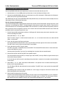
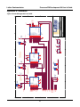
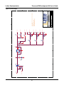
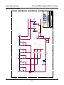
ProcessorPM™ Development Kit User’s Guide July 2009 Revision: EB45_01.0 Lattice Semiconductor ProcessorPM Development Kit User’s Guide Introduction Thank you for choosing the Lattice Semiconductor ProcessorPM Development Kit! This user’s guide describes how to start using the ProcessorPM Development Kit, an easy-to-use platform for evaluating and designing with the ProcessorPM-POWR605 (Processor Power Manager). Along with the evaluation board and accessories, this kit includes a pre-loaded Processor Support demonstration design. You may also reprogram the ProcessorPM to review your own custom designs. Note: Static electricity can severely shorten the lifespan of electronic components. See the ProcessorPM Development Kit QuickSTART Guide for handling and storage tips. Features The ProcessorPM Development Kit includes: • ProcessorPM Evaluation Board - The ProcessorPM board is a 2.5” x 2” form factor that features the following on-board components and circuits: – ProcessorPM-POWR605 – Power Manager II ispPAC®-POWR6AT6 – LEDs for general purpose I/O, power indicators, and watchdog timer interrupt indication – Slide potentiometer – USB B-mini connector for power and programming – 2x14 expansion header for general I/O, voltage monitor inputs, and power supply trim outputs – Push buttons for reset and watchdog timer trigger – 4-bit DIP switch for watchdog timer period programming and reset pulse stretch enable – JTAG and I2C header landings for ispDOWNLOAD™ cable programming and I2C interface • Pre-loaded Processor Support Demo - The kit includes a pre-loaded demo design that demonstrates watchdog timer, voltage supervisor, and reset generation features of the ProcessorPM. • USB Connector Cable - The ProcessorPM Evaluation Board is powered from the mini B USB socket when connected to a host PC. The USB channel also provides a programming interface to the ProcessorPM and POWR6AT6 JTAG ports. • QuickSTART Guide - Provides information on connecting the ProcessorPM Evaluation Board, running the preloaded processor support demo. • ProcessorPM Development Kit Web Page - The ProcessorPM Development Kit web page provides access to the latest documentation, demo designs, and drivers for the kit. The contents of this user’s guide include demo operation, programming instructions, top-level functional descriptions of the evaluation board, descriptions of the on-board connectors, switches and a complete set of schematics of the ProcessorPM board. Software Requirements You should install the following software before you begin developing designs for the evaluation board: • PAC-Designer® 5.1 • ispVM™ System 17.5 2 Lattice Semiconductor ProcessorPM Development Kit User’s Guide Figure 1. ProcessorPM Evaluation Board, Top Side Figure 2. ProcessorPM Evaluation Board, Bottom Side 3 Lattice Semiconductor ProcessorPM Development Kit User’s Guide ProcessorPM Device This board features the ProcessorPM, an in-system programmable, mixed-signal PLD that integrates high-performance analog voltage monitors, 4 timer counter blocks, and a 16-macrocell programmable logic device. A complete description of this device can be found in the ProcessorPM-POWR605 Data Sheet. Demonstration Designs Lattice provides two demos that illustrate key applications of the ProcessorPM and Power Manager II POWR6AT6 devices: • Processor Support - Demonstrates the ProcessorPM as a power manager for a processor, DSP, ASSP, or ASIC. It integrates three functions traditionally covered by discrete ICs: voltage supervisor, reset generator, and watchdog timer. The programmable features of the ProcessorPM highlight its flexibility to be used in a variety of system support roles. The processor support demo design is pre-loaded into the ProcessorPM by Lattice. Note: The processor support demo program (JEDEC) differs slightly from the Initial Factory Configuration described in the ProcessorPM-POWR605 Data Sheet. WDT_Intr output is active-high in the demo program, and active-low in the factory configuration. • Voltage Monitoring - Shows application of the ispPAC-POWR6AT6 to provide supply measurements via an I2C interface. The voltage monitoring support demo design is pre-programmed into the POWR6AT6 by Lattice. Note: It is possible that you may obtain your ProcessorPM board after it has been reprogrammed. To restore the factory default demo and program it with other Lattice-supplied examples see the Download Demo Designs and Download Windows Hardware Drivers section of this document. Processor Support Demo The processor support demo is pre-programmed into the non-volatile elements of the ProcessorPM and POWR6AT6 devices and is operational upon power-up. The design provides the following features: • Detect voltage supply violations and assert a CPU reset if a fault occurs. • Provide a 500 ms, 2 sec, 10 sec, or 1 min period watchdog timer and assert a watchdog timer interrupt if a timer expires before a watchdog trigger interrupt occurs. • Assert CPU reset pulses if manual reset of the board occurs. Provide an optional 200 ms pulse stretch of the reset. • Debounce manual reset input. A PAC-Designer software project (.pac) defines the analog trip points for the ProcessorPM voltage monitors, timercounter period, and supervisory equations that define logical functions. 4 Lattice Semiconductor ProcessorPM Development Kit User’s Guide Figure 3. Processor Support Demo Block Diagram DC-DC#1 3.3V (VMON1) DC-DC#3 1.8V (VMON3) DC-DC#2 2.5V (-5%) (VMON2) 1 VM3 SW1 8 R16 Power, Blue LED PWR-D1 Power Supply Bus Voltage Supervisor Reset_CPU Reset Generator Reset (SW2) CPU Reset or Power Fail (IO1-D2) WDT_Intr Watchdog Timer WDT_Trig ProcessorPM WDT Interrupt (D11) WD_Trig (SW3) 2 Processor/DSP WDT Sel SEL1, SEL0 (SW1) 00 = 500 ms 01 = 2 sec 10 = 10 sec 11 = 1 min Reset_Pulse RST (SW1) 0 = No Stretch 1 = 200 ms Stretch Table 1 describes the DIP switch, push-button inputs, and slide potentiometer settings that control the pre-configured ProcessorPM and emulate a variety of processor support scenarios. Use them as a reference as you follow the procedure. To indicate a ‘1’ (logical True) on the DIP switch SW1, slide the switch towards the number indicated on the switch body. Note the circuit board silkscreen markings for: VM3=1.8, RST=0, SEL0=0, and SEL1=0. Table 1. Processor Support Demo Switch and Button Settings Setting Function DIP Switch (1, 2, 3, 4) 500 ms WDT (SEL0=0, SEL1=0) Enables a 500 ms period watchdog timer (WDT). XX00 When active, the ProcessorPM will monitor the terminal count (TC) value a programmable timer. Once 500 ms expires, the WDT_Intr output is asserted. An amber WDT_INT LED (D11) will light momentarily to indicate the WDT interrupt input to the processor/DSP is active. Once activated, you may reset the WDT by pressing the push-button switch (WD_Trig) to emulate a WDT trigger event asserted by the processor/DSP. A red LED D5 will light when SEL0=0 and LED D6 will light when SEL1=0. Note: For the demonstration scenario, an additional transistor circuit of the evaluation board stretches WDT_Intr output period to make the interrupt event visible to the eye. XX10 2 sec WDT (SEL0=1, SEL1=0) Enables a 2-second period watchdog timer (WDT). XX01 10 sec WDT (SEL0=0, SEL1=1) Enables a 10-second period watchdog timer (WDT). XX11 1 min WDT (SEL0=1, SEL1=1) Enables a 1-minute period watchdog timer (WDT). X0XX Disable Reset Pulse Stretch (RST=0) Disables the reset pulse stretch option of ProcessorPM. A red LED D4 will light when RST=0. 5 Lattice Semiconductor ProcessorPM Development Kit User’s Guide Table 1. Processor Support Demo Switch and Button Settings (Continued) Setting X1XX 0XXX Function Enable 200 ms Reset Pulse Stretch (RST=1) Appends an additional 200 ms period to any processor/DSP reset output asserted by the ProcessorPM. Programmable clock and timer functions of the ProcessorPM allow for a variety of timeout intervals from 32 us to 1.96 sec in 128 steps. It may be necessary to connect a logic analyzer to detect the pulse stretch. 1.8V Supply OK (VM3=1.8) Connects the 1.8V supply rail to the voltage monitor input (VMON3) of the ProcessorPM. This setting emulates a stable 1.8V supply. 1.8V Supply Failure (VM3=High-Z) Disconnects the 1.8V supply rail from the voltage monitor input (VMON3) of the ProcessorPM. 1XXX This setting emulates a DC-DC converter or other supply failure on the PCB. The ProcessorPM will assert the Reset_CPU output signal to initiate a reset of the processor/DSP target device. A red LED (D2) will light to indicate the power fail condition. Push-button Switch WD_Trig WDT Trigger Press the push-button switch (WD_Trig) to emulate the watchdog timer reset trigger issued periodically for normal operation by the processor/DSP. Reset Manual Reset Press the push-button switch (Reset) to assert a manual reset of the evaluation board. All timers of the ProcessorPM will be cleared and the Reset_CPU output signal will be asserted. Slide Potentiometer R16 Voltage Supervisor Input A slide potentiometer emulates the variability of a 2.5V voltage rail on the PCB. Slide the pot towards the 0.0V position to lower the voltage level input to the ProcessorPM voltage monitor (VMON2). Connect to the ProcessorPM Evaluation Board To power and program the evaluation board you may use a PC USB port or use a combination of an external 5V power supply and a Lattice ispDOWNLOAD Cable (Parallel Port HW-DLN-3C). If your PC does not provide a USB port, see the “Add Support for the Lattice ispDOWNLOAD Cable (HW-DLN-3C)” section. USB Cable Connection Use the USB cable provided to connect the evaluation board to your PC: 1. Connect the USB cable from a USB port on your PC to the board’s USB mini-B socket (J1) on the bottom left side of the board. After connection is made, a blue Power LED (PWR) will light up indicating the board is powered on. 2. If you are prompted, “Windows may connect to Windows Update” select No, not this time from available options and click Next to proceed with the installation. Choose the Install from specific location (Advanced) option and click Next. 3. Select Search for the best driver in these locations and click the Browse button to browse to the Windows driver folder created in the Download Windows Hardware Drivers section. Select the CDM 2.04.06 WHQL Certified folder and click OK. 4. Click Next. A screen will display as Windows copies the required driver files. Windows will display a message indicating that the installation was successful. 5. Click Finish to install the USB driver. 6 Lattice Semiconductor ProcessorPM Development Kit User’s Guide ispDOWNLOAD Cable (HW-DLN-3C) Connection Use the ispDOWNLOAD cable (sold separately) to connect the evaluation board to your PC: 1. Connect external +5V and GND power to pad locations J5 and J6 (Schematic Sheet 5 of 5). 2. Connect the ispDOWNLOAD cable from a parallel port on your PC to the board’s JTAG header (J3) (Schematic Sheet 5 of 5) on the right side of the board. See “Add Support for the Lattice ispDOWNLOAD Cable (HW-DLN-3C)” for information on how to modify the evaluation board to add a JTAG header connection. Run the Processor Support Demo The ProcessorPM processor support demo illustrates key functions of the ProcessorPM: voltage supervisor, reset generator, and watchdog timer (WDT). The block diagram of the processor support demo, Figure 3, shows the ProcessorPM interface to a simulated processor/DSP. LEDs and switches are used to emulate the processor interface. Many processor power management scenarios can be shown with the ProcessorPM evaluation board. Follow the procedure below to emulate one particular case. 1. Set the ProcessorPM configuration to indicate 1.8V Supply OK, disable reset pulse stretch and enable a twosecond watchdog timer period. Select DIP Switch (1, 2, 3, 4) = 0010 Note: To indicate a logical 1, slide the switch towards the 1, 2, 3, or 4 numeral mark on the case. Select the R16 Slider = 3.3V position. 2. Press and then release the Reset push-button. The ProcessorPM Evaluation Board is reset. The CPU Reset LED (D2) lights to indicate the reset condition. The WDT timer is reset and the two-second WDT count begins. 3. Press and release the WD_Trig push-button. The WDT_Trig signal is asserted by the processor/DSP. The ProcessorPM timer/counter is reset and the twosecond watchdog timer restarts. Continue pressing the WD_Trig to “pet” the watchdog timer to prevent the two-second timeout. 4. Wait for two seconds and allow the WDT timer period to expire. The ProcessorPM asserts the WDT_Intr output signal and the WDT_Interrupt LED (D11) lights momentarily to indicate the interrupt condition. In the next step you will increase the watchdog timer period from 2 seconds to 10 seconds and enable Reset Pulse Stretch. 5. Select SW1 (1, 2, 3, 4) = 0101. Also select the R16 Slider = 3.3V position. Press and release the Reset pushbutton on the ProcessorPM board. The CPU Reset LED (D2) light indicates the reset condition. The WDT timer is reset and the 10-second WDT count begins. The following steps emulate a brown out condition of a 2.5V supply rail output of a DC-to-DC converter (DCDC#2) monitored by the ProcessorPM. 6. Slowly slide R16 towards the 0.0V position. Once the ProcessorPM voltage monitor detects the 2.5V supply rail has dropped below a 2.5V-5% threshold value a supply fault will be triggered and the Reset CPU output signal is asserted. The CPU Reset LED (D2) light indicates the reset condition. Note that the ProcessorPM watchdog timer is also disabled. 7 Lattice Semiconductor ProcessorPM Development Kit User’s Guide 7. Slide R16 toward the 3.3V position.Once the ProcessorPM voltage monitor detects that the 2.5V rail is above a threshold value of 2.5V -5%, the Reset CPU output signal is released. The CPU Reset LED (D2) light goes out. Run the Voltage Monitoring Demo The voltage monitor demo illustrates how to access the 2-wire I2C slave interface of the ispPAC-POWR6AT6 device to perform voltage level measurements. This is a popular means for a microcontroller/microprocessor to monitor voltages and adjust the voltage profiles of the POWR6AT6 DC-DC converter margin output drivers. For more information on POWR6AT6 end applications see AN6077 Stable Operation of DC-DC Converters with Power Manager Closed Loop Trim. This demo uses the ispPAC-POWR6AT6 I2C Utility software provided with PAC-Designer software running on a host PC to emulate a processor’s interface to the POWR6AT6. 1. Modify the evaluation board to use the Lattice ispDOWNLOAD Cable (HW-DLN-3C) for a PC parallel port. See the “Add Support for the Lattice ispDOWNLOAD Cable (HW-DLN-3C)” section for more information. 2. Install PAC-Designer software. 3. From the PAC-Designer<ver>\Macro directory, run PowerManager_6AT6_I2C_Utility.exe. For more information on the I2C Hardware Verification Utility software and operation see AN6067, ispPAC-POWR1220AT8 I2C Hardware Verification Utility User’s Guide. 4. Set I2C Address = 6Ah Download Demo Designs The processor support demo is preprogrammed into the ProcessorPM Evaluation Board, however over time it is likely your board will be modified. Lattice distributes source and programming files for demonstration designs compatible with the ProcessorPM board. To download demo designs: 1. Browse to the ProcessorPM Development Kit web page of the Lattice web site. Select the Demo Applications download and save the file. 2. Extract the contents of “ProcessorPM_DK_DemoSource.zip” to an accessible location on your hard drive. Two demo design directories (Demo_ProcessorPMDK_<demo>) are unpacked. Where: Demo Directories Processor Support Demo Demo_ProcessorPMDK_ProcessorSupport Voltage Monitoring with the POWR6AT6 Demo Demo_ProcessorPMDK_VoltageMonitoring Recompile a Demo Project with PAC-Designer Use the procedure described below to recompile any of the demo projects for the ProcessorPM Evaluation Board. 1. Install and license PAC-Designer software 2. Download the demo source files from the ProcessorPM Development Kit web page. 3. Run PAC-Designer. 4. Open the <demo>.pac project file. 5. From the schematic block diagram, double-click the Sequence Controller block. The LogiBuilder interface appears. 8 Lattice Semiconductor ProcessorPM Development Kit User’s Guide 6. Choose Tools > Compile LogiBuilder Design. After a few moments the JEDEC programming file is output. 7. See the Processor Support Demo section of this document for details on downloading a programming file to the board. Download Windows Hardware Drivers If you wish to reprogram the ProcessorPM Evaluation Board, you will need to obtain the necessary hardware drivers for Windows. If your installation of Windows does not automatically install USB drivers when the evaluation board is connected to a USB port, then use the procedure below to download them from the Lattice web site. To download Windows Hardware Drivers: 1. Browse to the ProcessorPM Development Kit web page, locate the hardware device drivers for the USB/JTAG interface. 2. Download the ZIP file to your system and unzip it to a location on your PC. Programming with ispVM The processor support and voltage monitoring demo designs are pre-programmed into the ProcessorPM Evaluation Board by Lattice. To restore a ProcessorPM Evaluation Board to factory settings or load an alternative demo design, use the procedures in this section. For more information see AN6062, Using ispVM System to Program ispPAC Devices. To install ispVM programming tools: 1. Install and license ispVM System software. 2. Connect the board to a host PC using the USB port or JTAG header connection. 3. Follow the USB Cable Interface or ispDOWNLOAD Cable Interface procedure below to program the evaluation board. USB Cable Interface The ProcessorPM Evaluation Board is equipped with a built-in USB-based programming circuit. This consists of a USB PHY and a USB connector. When the board is connected to a PC with a USB cable, it is recognized by the ispVM System software as a “USB Download Cable”. The ProcessorPM and POWR6AT6 can then be scanned and programmed using the ispVM System software. To program a demo programming file: 1. From the Start menu run ispVM System. ispVM appears. 2. Choose Options > Cable and IO Port Setup... The Cable and I/O Port Setup dialog appears. 3. Make the following selections: Cable Type: USB2 Port Setting: USB2 Click OK. 9 Lattice Semiconductor ProcessorPM Development Kit User’s Guide 4. Choose ispTools > Scan Chain. The New Scan Configuration Setup window appears. The POWR605 and POWR6AT6 device(s) appear in the device list. 5. Right-click the ispPAC-POWR605 or ispPAC-POWR6AT6 entry and choose Edit Device... The Device Information dialog appears. 6. From the Data File section, click the Browse button. The Open Data File dialog appears. 7. Browse to the <Demo Dir>\project folder, select <Demo>.jed, and click Open. From the Operation list choose FLASH Erase, Program, Verify and click OK. 8. Choose Project > Download. ispVM reprograms the evaluation board. Programming requires about 20-40 seconds. A small, timer window will appear to show elapsed programming time. At the end of programming, the configuration setup window should show a “PASS” in the “Status” column. ispDOWNLOAD Cable (Parallel Port HW-DLN-3C) Interface This section describes how to connect and reprogram the evaluation board using HW-DLN-3C. 1. Connect external +5V and GND power to pad locations J5 and J6. 2. Connect the HW-DLN-3C ispDOWNLOAD cable between J3 header and the parallel port of your PC. 3. Run ispVM software to program the ProcessorPM board. 4. Follow the procedure of “USB Cable Interface” to configure ispVM and download JEDEC files to selected devices. Use Cable Type “LATTICE” for Cable and I/O Port Setup. ProcessorPM Evaluation Board This section describes the features of the ProcessorPM evaluation board in detail. Overview The ProcessorPM Evaluation Board is a complete development platform for the Lattice ProcessorPM mixed-signal PLD. The board includes circuitry to emulate a processor/DSP interface, a USB program/power port, and an expansion header to support test connections. A Power Manager II ispPAC-POWR6AT6 is included and can be programmed to demonstrate power supply margin and trim applications. The board is powered by a PC USB port and you may reprogram the board using ispVM software. If no USB port is available for your PC, the board can be modified such that it can be powered with an external power supply and programmed with the ispDOWNLOAD cable (sold separately) from a PC parallel port. 10 Lattice Semiconductor ProcessorPM Development Kit User’s Guide Figure 4. ProcessorPM Evaluation Board Block Diagram 3.3V VMON1 IO_[1:5] Slide 2.5V Potentiometer VMON2 5 5 LEDs IO_2 Pulse Stretch Circuit 1.8V DIP Switch SW1A VMON3 VMON[1:6] 6 VMON_GS[4:6] 3 TRIM_[4:6] 3 IO_[1:5] 5 IN_[1:2] 2 VRAIL[4:6] 3 VMON[4:6] 4 DIP Switch SW1B,C,D A/Mini-B USB Cable USB Mini B Socket LED D11 IO_[3:5] Pushbutton Switch SW2 IN1 Pushbutton Switch SW3 IN2 3 24 ProcessorPM ispPACPOWR605-01SN24I HVOUT[1:2] JTAG Header JTAG USB Controller I2C VMON 2 6 VMON_GS 3 JTAG TRIM_[4:6] 3 Power Manager II ispPACPOWR6AT6-01SN32I 11 I2C 2 I2C Header 2 Header 14x2 Lattice Semiconductor ProcessorPM Development Kit User’s Guide Table 2 describes the components on the board and the interfaces it supports. Table 2. ProcessorPM Evaluation Board Components and Interfaces Component/Interface Type Schematic Reference Description Circuits Pulse Stretch Circuit Circuit Q4, D10, D11 Stretch watchdog interrupt pulse outputs to 40 ms. USB Controller Circuit U4:FT2232D USB-to-JTAG interface and dual USB UART/FIFO IC. USB Mini B Socket I/O J1:USB_MINI_B Programming and debug interface. Mixed Signal PLD U3: ispPAC-POWR6AT6 Voltage monitor, margin, trim. Mixed Signal PLD U1:ispPAC-POWR605 Watchdog timer, voltage supervisor, reset generator I/O J2:I2C I2C interface. Components Power Manager II ProcessorPM Interfaces 8x1 Header Landing 8x1 Header Landing I/O J3:JTAG Interface JTAG interface. 14x2 Header I/O J6:HEADER 14X2 User-definable I/O. 5 LEDs Output D7-D0 User-definable LEDs, I/O1 to I/O5. 4-bit DIP switch. DIP Switch I/O SW1A, B, C, and D Push-button Switches I/O SW2:Reset, SW3:WD_Trigger General-purpose push-buttons. Slide Potentiometer I/O R16 Potentiometer tied to 3.3V rail. Emulates brown-out 2.5V conditions at VMON2 inputs of ProcessorPM and POWR6AT6. Subsystems This section describes the principle sub-systems for the ProcessorPM Evaluation Board in alphabetical order. When reviewing the board, orient it so the silkscreen markings are readable. DIP Switch The evaluation board includes a four-bit input toggle switch located on the SE corner of the board. Three are available as general purpose inputs. Slide the switch toward the numeral mark on the switch case to indicate a logical ‘1’. Table 3. DIP Switch Reference Item Description Reference Designators SW1A, B, C and D Part Number 219-4MST Manufacturer CTS Web Site www.ctscorp.com Table 4. DIP Switch Pin Information SW1 Description ProcessorPM Pin D/4 Watchdog Delay SEL1 or user-defined input 15 C/3 Watchdog Delay SEL0 user-defined input 17 B/2 Reset Pulse Stretch enable or user-defined input 18 A/1 3.3V supply rails to VMON3 connection 4 12 Lattice Semiconductor ProcessorPM Development Kit User’s Guide Expansion Header The expansion header provides 28 user I/Os connected to the ProcessorPM and POWR6AT6. The remaining pins serve as power for expansion boards. The expansion connector is con• gured as one 16x2 100mil centered pin header. Table 5. Expansion Connector Reference Item Description Reference Designators J4 Part Number 90131-0800 Manufacturer Molex/Waldom Electronics Web Site www.molex.com Table 6. Expansion Header Pin Information J4 Pin Function ProcessorPM Pin POWR6AT6 Pin 1 +3.3V — — 2 +3.3V — — 3 IO_5 IN_OUT5 — 4 IO_4 IN_OUT4 — 5 IO_3 IN_OUT3 — 6 IO_2 IN_OUT2 — 7 IO_1 IN_OUT1 — 8 IN2 IN2 — 9 IN1 IN1 — 10 HVOUT2 — — 11 HVOUT1 — — 12 VMON2 VMON2 VMON2 13 VMON1 VMON1 VMON1 14 VMON3 VMON3 VMON3 15 VMON4 VMON4 VMON4 16 TRM4 — DAC4 17 VMON4_GS — VMON4GS 18 VRAIL4 — — 19 VMON5 VMON5 VMON5 20 TRM5 — DAC5 21 VMON5_GS — VMON5GS 22 VRAIL5 — — 23 VMON6 VMON6 VMON5 24 TRM6 — DAC6 25 VMON6_GS — VMON6GS 26 VRAIL6 — — 27 GND — — 28 GND — — 13 Other Connections Voltage supervisory circuit Voltage supervisory circuit Voltage supervisory circuit Lattice Semiconductor ProcessorPM Development Kit User’s Guide JTAG Interface Circuits For power and programming, an FTDI USB UART/FIFO IC converter provides a communication interface between a PC host and the JTAG programming chain of the ProcessorPM board. The USB 5V supply is also used as a source for the 3.3V and 1.8V supply rails. A USB B-type mini socket is provided for the USB connector cable. The evaluation board can be modified to use the Lattice ispDOWNLOAD cable (HW-DLN-3C) for programming. See the “Add Support for the Lattice ispDOWNLOAD Cable (HW-DLN-3C)” section for more information. Table 7. JTAG Interface Reference Item Description Reference Designators U4 Part Number FT2232D Manufacturer FTDI (Future) Web Site www.ftdichip.com Table 8. JTAG Programming Pin Information Signal Name Description ProcessorPM Pin POWR6AT6 TDO Test Data Output 11:TDO 4:TDI PM_TDO Test Data Output — 1:TDO PM_TDI Test Data Input 13:TDI — TMS_605 Test Mode Select 14:TMS — TMS_6AT6 Test Mode Select — 5:TMS PM_TCK Test Clock 12:TCK 3:TCK LEDs Five red LEDs (D2-D6) are used to reflect I/Os of the preprogrammed processor support demo. Three of the five LEDs are connected to DIP switch inputs. The LEDs are located in the center of the board, next to the expansion header. You may use D2-D6 for user-defined outputs for your own custom ProcessorPM designs. A blue LED (POWR - D1) is used to indicate USB 5V power. An amber LED (D11) is used to indicate interrupt events asserted by the ProcessorPM. Table 9. User LEDs Reference Item Description Reference Designators D2-D6 Part Number LTST-C190CKT Manufacturer Lite-On Web Site www.liteonit.com Table 10. LED Pin Information Signal Name Description (Processor Support Demo) ProcessorPM Pin D6 IO_5, Watchdog Delay SEL1 input 15 D5 IO_4, Watchdog Delay SEL0 input 17 D4 IO_3, Reset Pulse Stretch enable input 18 D3 IO_2, Watchdog timer interrupt (WDT_Intr) output 19 D2 IO_1, CPU Reset or Power Fail output 20 D1 USB 5V Power na D11 Watchdog Timer Pulse na 14 Lattice Semiconductor ProcessorPM Development Kit User’s Guide Power Manager II ispPAC-POWR6AT6 The POWR6AT6 device (ispPAC-POWR6AT6) on the board provides power supply margin and trim functions, analog input monitoring with an embedded 10-bit ADC in a 5x5 mm quad flat-pack package. Table 11. ProcessorPM PLD Reference Item Description Reference Designators U3 Part Number ispPAC-POWR6AT6-01-SN32I Manufacturer Lattice Semiconductor Web Site www.latticesemi.com Table 12. ispPAC-POWR6AT6 Pin Information Pin # Pin Function Board Connection Processor Support Demo 1 VMON1 VMON1 2 VMON2 VMON2 3 VCC — 4 VMON3 VMON3 5 VMON4 VMON4 6 VMON5 VMON5 7 VMON6 VMON6 8 GND — 9 GND — 10 VCCJ — 11 TDO TDO 12 TCK PM_TCK 13 TDI PM_TDI 14 TMS TMS_605 15 IN_OUT5 IO_5 16 VCC — 17 IN_OUT4 IO_4 18 IN_OUT3 IO_3 19 IN_OUT2 IO_2 20 IN_OUT1 IO_2 21 IN2 IN2 22 IN1_PWRDN\ IN1 23 NC — 24 NC — Power Supply A single 3.3V supply voltage for the board components is provided from the USB DEBUG connection. ProcessorPM-POWR605 The ProcessorPM PLD device (ispPAC-POWR605) on the board integrates voltage supervisor, watchdog timer, and reset generator functions in a 4x4 mm chip scale package. 15 Lattice Semiconductor ProcessorPM Development Kit User’s Guide Table 13. ProcessorPM PLD Reference Item Description Reference Designators U3 Part Number ispPAC-POWR605-01-SN24I Manufacturer Lattice Semiconductor Web Site www.latticesemi.com Table 14. ProcessorPM-POWR605 Pin Information Pin Function Board Connection Processor Support Demo 1 TDO PM_TDO 2 VCCJ — 3 TCK PM_TCK Pin # 4 TDI TDO 5 TMS TMS_6AT6 6 CLTENb CLTENb 7 VPS0 VPS0 8 VPS1 VPS1 9 CLTLOCK/SMBA — 10 SCL PM_SCL 11 SDA PM_SCA 12 VCCD — 13 VCCA — 14 VMON1GS — 15 VMON1 VMON1 16 VMON2GS — 17 VMON2 VMON2 18 VMON3GS — 19 VMON3 VMON3 20 VMON4GS VMON4_GS 21 VMON4 VMON4 22 VMON5GS VMON5_GS 23 VMON5 VMON5 24 VMON6GS VMON6_GS 25 VMON6 VMON6 26 TRIM6 TRIM6 27 TRIM5 TRIM5 28 TRIM4 TRIM4 29 TRIM3 — 30 TRIM2 — 31 TRIM1 — 32 GND — 16 Lattice Semiconductor ProcessorPM Development Kit User’s Guide Pulse Stretch Circuit The pulse stretch circuit (Schematic Sheet 4 of 5) produces a ~40 ms period pulse so watchdog timer interrupt outputs are visible to the eye. When active, an amber LED (D11) will light. The actual output pulse generated by the ProcessorPM is 6 µs. Push-button Switches The board has two momentary push-button switches (SW2 and SW3) to support the pre-loaded processor support demo. SW2 is tied to a ProcessorPM input pin (IN1) which asserts the Reset input. SW3 is tied to a ProcessorPM input pin (IN2) which asserts the watchdog trigger (WD_Trig) input. You may use SW2/SW3 for user-defined inputs for your own custom ProcessorPM designs. Table 15. Push-button Reference Item Description Reference Designators SW2, SW3 Part Number EVQ-Q2K03W Manufacturer Panasonic ECG Web Site www.panasonic.com/industrial/components/components.html Table 16. Push-button Pin Information Button Description (Pre-Programmed Processor Support) ProcessorPM Pin SW2 ProcessorPM board reset 22 SW3 Watchdog trigger input (WD_Trig) 21 Modifying the ProcessorPM Evaluation Board The ProcessorPM Evaluation Board provides landing areas for additional circuits to support the following functions: • Additional voltage supervisor input circuits • Measure power-down current draw of the ProcessorPM device • Bypass devices in the JTAG programming chain • Powering the board with an external 5V supply • Programming the board with an ispDOWNLOAD Cable for a PC parallel port • Interfacing to the PAC-Designer I2C Utility software for the POWR6AT6 Power Manager II Note: Modifying your board requires good electronics handling and PCB fabrication techniques to avoid damage. Add Support for the Lattice ispDOWNLOAD Cable (HW-DLN-3C) This section describes how to modify the ProcessorPM board to use the Lattice HW-DLN-3C ispDOWNLOAD cable for JTAG programming or I2C communications from a PC parallel port. The JTAG header interface is required if your PC does not provide a USB port interface and you wish to reprogram the board. The I2C header interface is required to communicate with the PAC-Designer POWR6AT6 I2C Utility program. To modify the evaluation board to support HW-DLN-3C: 1. Remove R45 (Schematic Sheet 2 of 5). 2. Install R35 (Schematic Sheet 2 of 5). 3. Install an 8-pin header at location J3 - JTAG Interface (Schematic Sheet 5 of 5). 4. Install R28 and R29 (Schematic Sheet 5 of 5). 5. Install an 8-pin header at location J2 - I2C Interface (Schematic Sheet 5 of 5). 17 Lattice Semiconductor ProcessorPM Development Kit User’s Guide See ispDOWNLOAD Cable (Parallel Port HW-DLN-3C) for information on programming through the J3 - JTAG header. Add Voltage Supervisor Circuits This section describes how to modify the ProcessorPM Evaluation Board for additional voltage supervisor demonstrations. Add a pair of resistors for each additional voltage monitor input channel that you require to the on-board voltage supervisor circuits (Schematic Sheet 3 of 5) at positions R21/R22, R23/R24, and R25/R26. Each supervisor circuit is a voltage divider with the following characteristics: • 1% accurate resistors • yk <= 3k ohms • Select x and y resistor values so VMON = 0.669V • Install Zener diodes if VRAIL > 5.5V • Remove 100k ohm for higher accuracy You may attach prototype circuits or test equipment to the VMON inputs using J4 - HEADER 14X2 (Schematic Sheet 5 of 5). For more information on sensor circuit interfaces to Power Manager II and ProcessorPM devices, see AN6041, Extending the Input Range of the ispPAC-POWR1208. Measure Power-Down Current of the ProcessorPM This section describes how to modify the ProcessorPM power supply connections to support current measurements. 1. Remove R43 and R44 (Schematic Sheet 1 of 5). 2. Install jumper at location J12 (PM_VCC) (Schematic Sheet 1 of 5). 3. Attach ammeter to pins 1 and 2 of J12. JTAG Chain Bypass This section describes how to selectively bypass the ProcessorPM or POWR6AT6 devices in the JTAG programming chain. 1. JTAG TMS bypass: Remove R42 (ProcessorPM TMS) or R41 (POWR6AT6 TMS) to bypass either device. To reverse the bypass you may install jumpers at locations J10 or J11 to reconnect the TMS circuit (Schematic Sheet 1 of 5). 2. Install 10k ohm resistors at locations R39 and R40 (Schematic Sheet 1 of 5). 3. JTAG TDI/TDO bypass: Install jumpers at locations J7 (Bypass 605/7) or J8 (Bypass 6AT6) to break the TDI/TDO circuit. Mechanical Specifications Dimensions: 2 1/2 in. [L] x 2 in. [W] x 3/8 in. [H] Environmental Requirements The evaluation board must be stored between -40° C and 100° C. The recommended operating temperature is between 0° C and 55° C. The evaluation board can be damaged without proper anti-static handling. 18 Lattice Semiconductor ProcessorPM Development Kit User’s Guide Glossary CPLD: Complex Programmable Logic Device DIP: Dual in-line package. I2C: Inter-Integrated Circuit. LED: Light Emitting Diode. Mixed-Signal PLD: A PLD integrated with analog and mixed signal support circuitry. PCB: Printed Circuit Board. RoHS: Restriction of Hazardous Substances Directive. PLL: Phase Locked Loop. SPI: Serial Peripheral Interface. SRAM: Static Random Access Memory. TransFR™: Transparent Field Reconfiguration. UART: Universal Asynchronous Receiver/Transmitter. USB: Universal Serial Bus. WDT: Watchdog timer Ordering Information Description Ordering Part Number ProcessorPM Development Kit China RoHS Environment-Friendly Use Period (EFUP) PACPOWR605-P-EVN Technical Support Assistance Hotline: 1-800-LATTICE (North America) +1-503-268-8001 (Outside North America) e-mail: [email protected] Internet: www.latticesemi.com Revision History Date Version July 2009 01.0 Change Summary Initial release. 19 A B C D VPS0 VPS1 CLTENb VMON4_GS VMON5_GS VMON6_GS PM_SCL PM_SDA PM_TDO HVOUT2 HVOUT1 IO_5 IO_4 IO_3 IO_2 IO_1 5 22 21 13 11 14 12 IN1 IN2 PM_TDI PM_TCK 1 2 4 5 6 7 TDO +3.3V VMON1 VMON2 VMON3 VMON4 VMON5 VMON6 PM_TMS 5 TDI TDO TMS TCK IN1 IN2 10 VCCJ R32 100 DI PM_TDI 4 TDO J8 Bypass 6AT6 DNI PM_TDO 12 TMS_605 4 VCC HVOUT1 HVOUT2 VCCJ 13 VCCJ 3 11 GND IN/OUT3 IN/OUT4 IN/OUT5 IN/OUT6 IN/OUT7 ispPAC-POWR0607 9 TDI TDO TMS TCK IN1 IN2 8 J7 Bypass 605/7 DNI 18 14 19 15 21 VCCPM VCC VMON1 VMON2 VMON3 VMON4 VMON5 VMON6 U2 3 27 26 23 22 20 30 31 Remove R41 & 42. And install R39 & R40 to enable bypass feature. GND R30 100 DI 29 28 IN1 IN2 PM_TDI TDO PM_TCK 2 3 5 6 7 10 R39 10k DNI VMON1 VMON2 VMON3 VMON4 VMON5 VMON6 +3.3V GND R31 100 DI 20 19 18 17 15 DI 0 R42 Install ispPAC-POWR605 of ispPAC-POWR607 but not both. R44 0 DI J10 605/7 TMS DNI 1 2 GND IN_OUT1 IN_OUT2 IN_OUT3 IN_OUT4 IN_OUT5 ispPAC-POWR605 16 VCC 3 VCC VMON1 VMON2 VMON3 VMON4 VMON5 VMON6 U1 VCCPM VCCJ Remove R43 & 44. And install J12 to Measure Power Down Current. +3.3V 4 C1 100n DI VCCPM IO_1 IO_2 IO_3 IO_4 IO_5 C3 100n DI HVOUT1 HVOUT2 C2 100n DI VCCJ DI 0 R41 2 C4 100n DI 2 C5 100n DI +3.3V R40 10k DNI U3 TQFN_32 DI TDI TMS TCK TDO CLTENb VPS0 VPS1 Date: Size B DAC6 DAC5 DAC4 DAC3 DAC2 DAC1 VCCD VCCA VCCJ 32 10 11 9 26 27 28 29 30 31 12 13 2 +3.3V 1 Friday, 29-May-2009 Project ProcessorPM Evaluation Board 1 Sheet B B Schematic Rev Board Rev 1 of 5 TRIM_6 TRIM_5 TRIM_4 Lattice Semiconductor Applications Email: [email protected] Phone (503) 268-8001 -or- (800) LATTICE GND SCL SDA CLTLOCK/SMBA ispPAC-POWR6AT6 VMON1 VMON1GS VMON2 VMON2GS VMON3 VMON3GS VMON4 VMON4GS VMON5 VMON5GS VMON6 VMON6GS Title Power Manager 605/7 and 6AT6 4 5 3 1 6 7 8 15 14 17 16 19 18 21 20 23 22 25 24 TMS_6AT6 +3.3V PM_TCK CLTENb VPS0 VPS1 VMON4 VMON4_GS VMON5 VMON5_GS VMON6 VMON6_GS VMON3 VMON2 VMON1 J11 6AT6 TMS DNI 1 2 1 2 DI 0 R43 J12 PM_VCC DNI 1 2 20 1 2 A B C D Lattice Semiconductor ProcessorPM Development Kit User’s Guide Appendix A. Schematic Figure 5. Power Manager 605/7 and 6AT6 A B C D C11 10nF DI NC GND DD+ VCC 5 MH1 MH2 10 11 6 7 8 9 4 5 2 3 1 USB_MINI_B DI CASE CASE USB_MINI_B CASE CASE J1 USB Connection 5 DI 100k C12 10nF R2 27 DI R1 27 DI C13 33pF DI C10 0.1uF DI +5V_USB 18pF = 12pF + Ground Plane ( 6pF ) R3 DI L1 Ferrite_bead SM/R_0603 DI SHLD +5V_USB 4 C15 12pF DI 1 X1 1.5k R4 2 CS SK DIN DOUT 1 2 3 4 XTAL_HCM49 DI 6MHz DI 10k M93C46-W DI SOG.050/8/WG.244/L.225 VCC NC ORG GND U6 R10 DI 8 7 6 5 C14 33pF DI 4 R9 DI C16 12pF DI 1k R8 2.2k EECS EESK EEDATA DI R7 1M DI C23 0.1uF DI R6 10k DI 3 47 2 1 48 4 44 43 5 7 8 6 3 TEST EEDATA EESK EECS RESET# XTOUT XTIN RSTOUT# USBDP USBDM 3V3OUT C6 0.1uF DI VCCA R5 470 DI +5V_USB R45 0 DI DI TQFP_48 U4 FT2232D PWREN# SI/WUB TXDENB# SLEEPB# RXLEDB# TXLEDB# TXDB RXDB RTSB# CTSB# DTRB# DRSB# DCDB# RIB# SI/WUA TXDENA SLEEPA# RXLED# TXLED# TXDA RXDA RTSA# CTSA# DTRA# DSRA# DCDA# RIA# 41 26 30 29 28 27 40 39 38 37 36 35 33 32 10 15 13 12 11 0.1uF DI 0.1uF DI 1 2 C8 24 23 22 21 20 19 17 16 +3.3V C7 VCCIO 3 42 46 AVCC AGND VCC VCC 45 14 31 VCCIOA VCCIOB GND GND GND GND 21 9 18 25 34 R20 0 DI C9 0.1uF DI 2 R35 10k DNI +3.3V J9 Enable 2232 I/O DNI U5 4S1 4S2 3S1 3S2 2S1 2S2 1S1 1S2 11 13 7 9 3 5 15 1 DI TQFN_16 Date: Size B PM_SCL IO_1 IO_2 IO_3 IO_4 IO_5 WD_PULSE PM_TMS PM_TDO PM_TDI PM_TCK PM_SDA 1 Friday, 29-May-2009 Project ProcessorPM Evaluation Board 1 Sheet B B Schematic Rev Board Rev 2 of 5 JTAG TO POWR 605/7 & 6AT6 Lattice Semiconductor Applications Email: [email protected] Phone (503) 268-8001 -or- (800) LATTICE PWR_ENABLEb CLTENb VPS0 VPS1 STG3690QTR GND 1-2IN 3-4IN D1 D2 D3 D4 VCC Title USB to JTAG and I2C Interface 6 2 10 16 4 8 12 14 Remove R45 and install R35 to use J3 for JTAG programming. 2 A B C D Lattice Semiconductor ProcessorPM Development Kit User’s Guide Figure 6. USB to JTAG and I2C Interface 22 A B C D PWR_ENABLEb +5V_USB 5 C17 0.33uF DI 5 Q1 R11 10k DI R12 1M DI DI IRLML6402PbF D1 Blue DI SM/LED_0603 +5V 4 4 R13 10k DI C18 10uF DI 3 IN U7 1 GND 2 4 NCP1117 DI OUT TAB +3.3V C19 6.8uF DI 3 3 R15 1k DI R14 820 DI R19 100k DI R18 100k DI R17 100k DI 1 3 2 1 D9 MAZ80510GML 5.1V DNI D8 MAZ80510GML 5.1V DNI D7 MAZ80510GML 5.1V DNI R16 1k DI 8 R25 yk DNI R26 xk DNI R23 yk DNI R24 xk DNI R21 yk DNI R22 xk DNI SW_SPST_4 SW1A R34 1k DI R33 1k DI 2 VMON6 VRAIL6 VMON5 VRAIL5 VMON4 VRAIL4 VMON3 VMON2 VMON1 2 Date: Size B Friday, 29-May-2009 Project ProcessorPM Evaluation Board Title Power Supply 1 Sheet Lattice Semiconductor Applications Email: [email protected] Phone (503) 268-8001 -or- (800) LATTICE B B Schematic Rev Board Rev 3 of 5 Optional Off-board Voltage Dividers for Factory Configuration Use 1% resistors yk <= 3k Select xk so VMON = 0.669V Install Zener diodes if VRAIL > 5.5V Remove 100k for higher accuracy 1 A B C D Lattice Semiconductor ProcessorPM Development Kit User’s Guide Figure 7. Power Supply 23 A B C D IO_5 IO_4 IO_3 IO_2 IO_1 7 8 RN1G 9 RN1H 6 5 D6 Red DI 2.2k DI 2.2k DI +3.3V R49 470 DI D5 Red DI 2.2k DI 2.2k DI D4 Red DI 2.2k DI 3 WD_SEL0 2 4 2 2.2k DI RN1B WD_SEL1 RN1A 4 4 5 D3 Red DI 2.2k DI RN1C 7 SW_SPST_4 SW1B SW_SPST_4 6 SW_SPST_4 SW1C D10 1N4148 DI 3 SW1D 5 us Watchdog Timeout Pulse 1 10 RN1F 5 RN1E +3.3V +3.3V 5 4 0 1 0 1 D2 Red DI 9 3 500ms 2 sec. 10 sec. 1 min. 2.2k DI RN2H R46 4.7M DI Watchdog Delay 8 2.2k DI RN2G Reset Pulse Stretch Open = 200ms Closed = No Stretch 0 0 1 1 SEL1 SEL0 2.2k DI RN1D 3 DI C24 330pF 7 D11 Amber DI R47 470 DI Q4 FDV301N DI +3.3V 2.2k DI RN2F 6 5 +3.3V R48 10k DI 2.2k DI RN2E 3 4 SW2 Reset DI 2 2 1 Date: Size B SW3 WD_Trigger DI WD_PULSE IN2 IN1 1 Friday, 29-May-2009 1 Sheet Lattice Semiconductor Applications Email: [email protected] Phone (503) 268-8001 -or- (800) LATTICE 3 4 Project ProcessorPM Evaluation Board Title LEDs and Switches 500 ms Watchdog Pulse 2 1 2 B B Schematic Rev Board Rev 4 of 5 A B C D Lattice Semiconductor ProcessorPM Development Kit User’s Guide Figure 8. LEDs and Switches A B C D 5 IO_5 IO_3 IO_1 IN1 HVOUT1 VMON1 VMON4 VMON4_GS VMON5 VMON5_GS VMON6 VMON6_GS +3.3V 2 4 6 8 10 12 14 16 18 20 22 24 26 28 C22 100n DI TRIM_6 FID2 FIDUCIAL C21 100n DI TRIM_5 FID1 FIDUCIAL C20 100n DI R38 100 DI R36 100 DI TRIM_4 G4 CE Mark TRM6 TRM5 TRM4 R37 100 DI G3 E-Friendly 4 VRAIL6 VRAIL5 VRAIL4 IO_4 IO_2 IN2 HVOUT2 VMON2 VMON3 G2 WEEE +3.3V G1 Lattice Logo HEADER 18X2 1 3 5 7 9 11 13 15 17 19 21 23 25 27 J4 DI 1 J6 GND DNI 1 +5V 1 J5 +5V DNI 4 1 5 1 24 1 3 3 PM_SCL PM_SDA Q3 2N3904 DNI 1 10 +3.3V 2 2.2k DI 3 1 RN2C 2 Q2 2N3904 DNI 3 +3.3V 2.2k DI RN2A 2 2 2.2k DI R27 4.7k DNI 4 +3.3V Date: Size B +3.3V 1 2 3 4 5 6 7 8 1 2 3 4 5 6 7 8 Friday, 29-May-2009 Project ProcessorPM Evaluation Board 1 Sheet J3 I2C DNI J2 B B Schematic Rev Board Rev 5 of 5 JTAG Interface DNI Lattice Semiconductor Applications Email: [email protected] Phone (503) 268-8001 -or- (800) LATTICE 2.2k DI RN2D SCL SDA SDIN R28 4.7k DNI Title (Optional) JTAG, I2C, and Test Headers RN2B PM_TCK PM_TMS PM_TDO PM_TDI R29 4.7k DNI +3.3V 1 A B C D Lattice Semiconductor ProcessorPM Development Kit User’s Guide Figure 9. (Optional) JTAG, I2C and Test Headers Lattice Semiconductor ProcessorPM Development Kit User’s Guide Appendix B. Bill of Materials Table 17. Bill of Materials Item Quantity Reference Part Number 1 1 U1 ispPAC-POWR605 2 0 U2 ispPAC-POWR607 3 1 U3 ispPAC-POWR6AT6 4 1 U4 FT2232D 5 1 U5 STG3690QTR 6 1 U6 M93C46-WMN6TP 7 1 U7 NCP1117ST33T3G 8 1 D1 LTST-C190TBKT 9 1 D2 LTST-C190CKT 10 4 D3-D6 LTST-C190AKT 11 13 C1-10, 20-22 ECJ-1VB1C104K 12 2 C11,12 ECJ-1VB1C103K 13 2 C13,14 ERB1885C2E330JDX5D 14 2 C15,16 ERB1885C2E120JDX5D 15 1 C17 ECJ-1VB0J334K 16 1 C18 ECJ-2YB1A105K 17 1 C19 F920J106MPA 18 1 Q1 IRLML6402PbF 19 1 J1 UX60-MB-5ST 20 1 J4 90131-0800 21 1 R16 RA2043F-20-10EB1-B1K 22 2 R7,R12 ERJ-3GEYJ105V 23 4 R3,R17-19 ERJ-3GEYJ104V 24 3 R6,R10,R11 ERJ-3GEYJ103V 25 1 R9 ERJ-3GEYJ222V 26 1 R4 ERJ-3GEYJ152V 27 4 R8,R15,R33,R34 ERJ-3GEYJ102V 28 1 R14 ERJ-3GEYJ821V 29 2 R5,R13 ERJ-3GEYJ471V 30 6 R30-32, R36-38 ERJ-3GEYJ101V 31 2 R1,2 ERJ-3GEYJ270V 32 6 R20,R41-45 ERJ-3GEY0R00V 33 1 SW1 219-4MST 34 2 SW2, SW3 EVQ-Q2K03W 35 1 L1 HI0603P600R-10 36 1 X1 HCM49 6.000MABJ-UT 37 2 RN1, RN2 746X101222JP 38 3 n/a 382811-9 39 4 n/a SJ-5003 40 1 n/a n/a 41 1 n/a n/a 25 Lattice Semiconductor ProcessorPM Development Kit User’s Guide Table 18. Optional Parts Item Quantity Reference Part Number 1 6 J7-J12 2 2 J2, J3 3 2 J5, J6 4 3 R27-R29 ERJ-3GEYJ472V 5 3 R35,R39,R40 ERJ-3GEYJ103V 6 2 Q2,Q3 MMBT2369A 7 3 D7-D9 MAZ80510GML 8 6 R21-R26 26