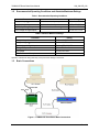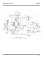
1
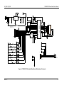
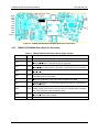
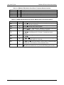
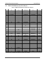
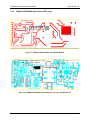
Simplifying System IntegrationTM
73M2901CE
Demo Board User Manual
March 17, 2010
Rev. 1.5
UM_2901CE_026
73M2901CE Demo Board User Manual
UM_2901CE_026
© 2010 Teridian Semiconductor Corporation. All rights reserved.
Teridian Semiconductor Corporation is a registered trademark of Teridian Semiconductor Corporation.
Simplifying System Integration is a trademark of Teridian Semiconductor Corporation.
All other trademarks are the property of their respective owners.
Teridian Semiconductor Corporation makes no warranty for the use of its products, other than expressly
contained in the Company’s warranty detailed in the Teridian Semiconductor Corporation standard Terms
and Conditions. The company assumes no responsibility for any errors which may appear in this
document, reserves the right to change devices or specifications detailed herein at any time without
notice and does not make any commitment to update the information contained herein. Accordingly, the
reader is cautioned to verify that this document is current by comparing it to the latest version on
http://www.teridian.com or by checking with your sales representative.
Teridian Semiconductor Corp., 6440 Oak Canyon, Suite 100, Irvine, CA 92618
TEL (714) 508-8800, FAX (714) 508-8877, http://www.teridian.com
2
Rev. 1.5
UM_2901CE_026
73M2901CE Demo Board User Manual
Table of Contents
1
Introduction ................................................................................................................................... 5
1.1 Getting Started......................................................................................................................... 5
1.2 Recommended Operating Conditions and Absolute Maximum Ratings ..................................... 6
1.3 Basic Connections ................................................................................................................... 6
2
3
Design Considerations .................................................................................................................. 7
73M2901CE EVM-600 Demo Board ............................................................................................... 8
3.1 Using the 73M2901CE EVM-600 Demo Board ......................................................................... 8
3.2 73M2901CE EVM-600 Hardware Design ................................................................................. 9
3.2.1
73M 2901CE EVM-600 Schematic Diagrams ............................................................. 9
3.2.2
73M2901CE EVM-600 Demo Board Pin Description ................................................ 12
3.2.3
73M2901CE-EVM-600 Demo Board Bill of Materials ................................................ 14
3.2.4
73M2901CE-EVM-600 Demo Board PCB Layout ..................................................... 15
4
73M2901CE EVM-WW Demo Board............................................................................................. 17
4.1 Using the 73M2901CE0-EVM-WW Demo Board .................................................................... 17
4.2 73M2901CE EVM-WW Hardware Design ............................................................................... 19
4.2.1
73M 2901CE EVM-WW Schematic Diagrams .......................................................... 19
4.2.2
73M2901CE EVM-WW Demo Board Pin Description................................................ 22
4.2.3
73M2901CE EVM-WW Demo Board Bill of Materials ............................................... 24
4.2.4
Recommended Components Used in the Demo Boards ........................................... 25
4.2.5
73M2901CE EVM-WW Demo Board PCB Layout .................................................... 28
5
DC Loop Circuit Schematic ......................................................................................................... 29
6
Related Documentation ............................................................................................................... 29
7
Contact Information..................................................................................................................... 29
Revision History .................................................................................................................................. 30
Rev. 1.5
3
73M2901CE Demo Board User Manual
UM_2901CE_026
Figures
Figure 1: T73M2901CE Demo Board Basic Connections ......................................................................... 6
Figure 2: 73M2901CE EVM-600 Demo Board Schematic....................................................................... 10
Figure 3: 73M2901CE EVM-600 Motherboard Schematic ...................................................................... 11
Figure 4: 73M2901CE EVM-600 Demo Board Pin Connections ............................................................. 12
Figure 5: 73M2901CE EVM-600 Demo Board: Bottom Layer ................................................................. 15
Figure 6: 73M2901CE EVM-600 Demo Board: Top Layer ...................................................................... 15
Figure 7: 73M2901CE EVM-600 Demo Board: Top Silk Screen ............................................................. 16
Figure 8: 73M2901CE Worldwide Demo Board: Daughter Board Schematic .......................................... 20
Figure 9: 73M2901CE Worldwide Demo Board: Motherboard Schematic ............................................... 21
Figure 10: 73M2901CE Worldwide Daughter Board Pin Connections ..................................................... 22
Figure 11: 73M2901CE Worldwide Demo Board: Bottom ....................................................................... 28
Figure 12: 73M2901CE Worldwide Demo Board: Top Layer and Silk Screen ......................................... 28
Figure 13: Simple DC Loop Simulator .................................................................................................... 29
Tables
Table 1: Recommended Operating Conditions ......................................................................................... 6
Table 2: Absolute Maximum Ratings ........................................................................................................ 6
Table 3: Termination Impedance Network Values .................................................................................... 8
Table 4: 73M2901CE EVM-600 Demo Board Description: Digital Interface ............................................ 12
Table 5: 73M2901CE EVM-600 Demo Board: Telephone Network Interface .......................................... 12
Table 6: 73M2901CE EVM-600 Demo Board: DB-25 RS-232 Level Serial Interface ............................... 13
Table 7: 73M2901CE EVM-600 Demo Board Bill of Materials ................................................................ 14
Table 8: S-register Settings for Worldwide Modem Design ..................................................................... 17
Table 9: Termination Impedance Network Values .................................................................................. 17
Table 10: Worldwide Country AC Impedance Requirements .................................................................. 18
Table 11: 73M2901CE Worldwide Demo Board: Digital Interface ........................................................... 22
Table 12: 73M2901CE Worldwide Demo Board: Telephone Network Interface ....................................... 23
Table 13: 73M2901CE Worldwide Demo Board: DB-25 RS-232 Level Serial Interface ........................... 23
Table 14: 73M2901CE Worldwide Demo Board Bill of Materials ............................................................. 24
Table 15: Transformers and Suppliers Tested and Used with the 73M2901CE....................................... 25
Table 16: EMI Inductors for the Tip/Ring Signal Path ............................................................................. 25
Table 17: Recommended PTC Fuses for CPE Applications ................................................................... 26
Table 18: Recommended TVS Over Voltage Protectors ......................................................................... 27
4
Rev. 1.5
UM_2901CE_026
73M2901CE Demo Board User Manual
1 Introduction
The Teridian Semiconductor Corporation 73M2901CE Demo Board is a platform for evaluating the
73M2901CE single-chip modem ICs. It incorporates the 73M2901CE integrated circuit, and it has been
designed to operate with a PC using the serial COM1 or COM2 RS-232 level ports and standard
communications software packages such as HyperTerminal.
This document describes the two available demo board configurations, the 73M2901CE-EVM-600 and
the 73M2901CE-EVM-WW.
The 73M2901CE EVM-600 is a board fitted with 600 Ω resistive termination and is suitable for use in USA
and Japan. This board has been designed to comply with U.S. Part 68, USA, and AS/ACIF S002:2001.
The 73M2901CE EVM-WW has selectable terminations, which makes it suitable for use in many different
countries worldwide. The board has been designed to comply with FCC Part 68, ETSI TS 203, JATE and
AS/ACIF S002:2001.
1.1
Getting Started
Figure 1 shows the basic connections of the Demo Board.
• Use the supplied motherboard and 5 V power supply.
• The motherboard includes a 3.3 V regulator to power the 73M2901CE Demo Board.
• The motherboard also includes RS-232 level shifters and DCE connector to connect the demo board
to a PC or other terminal device.
• Use a standard PC terminal emulation program to communicate with the 73M2901CE Demo Board.
See the 73M2901CE AT Command User Guide for a complete list of commands.
• Type “AT” on the terminal at any speed from 1200 bps to 9.6 Kbps to verify communications with the
modem are working correctly. The 73M2901CE modem will return “OK” if communication is properly
established.
• Connect the RJ-11 connector to a telephone network emulator or private branch exchange (BPX).
The demo board, although meeting all the required telecom standards, is not a certified device.
Therefore the 73M2901CE Demo Board should not be connected to the outside telephone network.
It is not possible to connect two 73M2901CE demo boards back-to-back to test their operation. A DC
loop current is needed to activate the network-side circuitry. A simple current-mirror current-source circuit
can be used to provide the required DC loop current. A simple circuit is shown in Figure 13. This circuit
supplies two independent sources, one for each modem. The loop current provided is approximately 20
mA to each modem. This circuit does not provide network impairments, call progress signals, or
attenuation, which are also typically used for modem testing.
Rev. 1.5
5
73M2901CE Demo Board User Manual
1.2
UM_2901CE_026
Recommended Operating Conditions and Absolute Maximum Ratings
Table 1: Recommended Operating Conditions
Parameter
Conditions
Rating
Supply Voltage VDD
At the demo board power pins
2.7 to 3.6 VDC
Supply Voltage VPC
At the mother board power connector
4.75 to 5.5 VDC
Ambient Operating Temperature
Without condensation or icing
-40 °C to +85 °C
Input Voltage for Digital Inputs
0 V to VDD + 0.3 V
Table 2: Absolute Maximum Ratings
Parameter
Rating
Supply Voltage VDD
-0.5 to 4.0 VDC
Supply Voltage VPC
-0.5 to 6.0 VDC
Input Voltage for Digital Inputs
-0.3 to (VDD+0.5) VDC
Storage Temperature
-60 to 150 °C
Pin Voltage
-0.3 to 5.5 V VDC
ESD Tolerance – Other pins
+/- 2kV
Operation outside these rating limits may cause permanent damage to the device.
1.3
Basic Connections
Figure 1: T73M2901CE Demo Board Basic Connections
6
Rev. 1.5
UM_2901CE_026
73M2901CE Demo Board User Manual
2 Design Considerations
Keep OSCIN and OSCOUT signals as short as possible and locate the crystal near the pins. Use an
11.0592 MHz parallel mode crystal only. Do not use ground planes under the oscillator circuit since this
will increase the parasitic capacitance on the pins. The values of C2 and C3 depend on the load
capacitance rating of the crystal that is used, not the 73M2901CE. This load capacitance will typically be
between 15 pF and 27 pF, but usually 18 or 22 pF. Parallel resonant crystals are tuned with a specific
capacitive load and will be within their specifications when this load is used. This rating is the
capacitance measured between the crystal pins including all parasitic capacitances. It is not the values of
the capacitors used. The selection of these capacitors can vary with the layout of the PCB, so do not
assume the values used with the 73M2901CE demo board are correct for all designs.
System noise is the most likely cause of poor Caller ID and low-level receive performance. The lowest
amplitude signals that the modem will need to receive are on the order of 5 mV rms. The Caller ID
receive levels are also very low due to the requirement to have a high (60 kΩ) AC input impedance while
on hook. Having a 20 dB gain boost during Caller ID reception compensates for this, but if there is
excessive noise, it will also be amplified. Keeping the analog and digital grounds separate helps control
the amount of noise that gets to the receiver input. Dramatic improvements in low-level performance can
be gained by proper layout.
Keep the VCC trace as short as possible. Make the power trace a minimum of 0.5 mm thick. The analog
and digital power and ground should be kept separate for best low receive level performance. Route the
power to the digital pins and bypass capacitors on one net and the analog power and VBG bypass pins
on another net with inductors separating the two. If power planes are used, separate the power and
ground planes so there are separate analog and digital planes for the 73M2901CE.
Keep 0.1 µF and 3.3 µF bypass capacitors close to VPD power pins of the device and take other end to
the digital ground.
Keep 0.1 µF and 10 µF bypass capacitors close to VPA power pin of the device and directly connect the
other end to analog ground.
Keep all analog signaling away from any high-speed digital circuitry and traces that may be on the board.
Observe the separation of the network and modem side circuitry. Maintain at least ¼ inch (6 mm)
separation between the two. Do not run power planes under the network side circuitry and maintain the
same spacing for the planes from the network. Use only UL, CSA, or TUV approved components that
cross the isolation barrier or for network protection to assure compliant performance for the DAA.
The transformer used for coupling will have an influence on the values of the components in the DAA
circuitry. The winding resistance, inductances and other characteristics of the transformer affect the
values of the impedance matching components. Make sure you have the transformer manufacturer’s
recommended circuit values when using other transformers. The values can be determined through
simulations, but may still require some adjustment to optimize the design.
Rev. 1.5
7
73M2901CE Demo Board User Manual
UM_2901CE_026
3 73M2901CE EVM-600 Demo Board
During the past several years, there have been significant changes to the way telecommunications device
certification is handled. Previously you were required to take your new product to an authorized
certification laboratory to have certification testing performed. The United States has fundamentally
changed their approval procedures for telephone equipment. They have introduced the concept of SDoC
(Self-Declaration of Conformity), implying that formal approval of a TCB (Telecommunication Certification
Body) is not further necessary. The definition of the technical requirements has been delegated to
industry. There is a choice of conformity testing but, in general, the manufacturer or his authorized
representative must maintain technical documentation that includes a declaration of conformity and
shows how compliance is achieved. It is still a requirement to meet all the same technical requirements
for electrical compatibility with the network (TIA/EIA/IS-968 (Part 68) ), electrical safely (UL-60950 power
cross) and EMI (Part 15 radiated emissions). Unless you are equipped to perform the tests to verify the
operation of your product, it is still prudent to use a third party testing laboratory to assure compliance
with applicable regulations. The ACTA (Administrative Council for Terminal Attachments) is the body that
now administers the telecom terminal equipment. The FCC is no longer involved in any aspect of the
process. The ACTA is a privatized organization and administers all aspects of the telecom equipment.
See http://www.part68.org for information on the ACTA.
The 73M2901CE Demo Board is designed to meet all the applicable certification regulations defined in
those regulations. The 73M2901CE EVM-600 Demo Board design is intended for use in countries that
use a 600 Ω resistive termination. Although designed to meet the ACTA defined specifications, the
73M2901CE EVM-600 demo board is not a certified device, and it is therefore not intended for use on the
PSTN network. It should only be used in a laboratory environment with network simulation equipment.
The network input protection is now standard worldwide, so finding components that that meet UL-60950
Power Cross requirements are not too difficult. Input current limiting and over-voltage protection are both
universally required or advised. Self-resetting PPTC fuses are now available that not only protect the
product but eliminate the need to replace parts if they are tripped. These protection devices tend to be
some of the more expensive components in the design, but to scrimp on these in the initial design can
cause problems latter when fixing the problem is more expensive.
3.1
Using the 73M2901CE EVM-600 Demo Board
The schematic in Figure 2 shows the design for the 73M2901CE EVM-600 Demo Board. The design
uses a “wet transformer” that uses the transformer as the DC load on the line. The advantage to using
this topology is that the BOM cost can be lower compared to a “dry transformer” which passes the DC
current through an external circuit that simulates an inductor. A dry transformer can be made much
smaller, so if small size is important, a dry transformer is preferred.
Table 3 shows the termination impedances for 600 Ω resistive as well as ETSI TS 203 and Australian
complex impedances. With these three terminations, worldwide terminations impedance requirements
can be met. Other demo boards are available to support these other terminations. The 73M2901CE
EVM-600 Demo Board uses a wet transformer design that has a 600 Ω resistive termination.
Table 3: Termination Impedance Network Values
Termination
600 Ohm
ETSI TS 203 complex
Australia
8
Terminator Component Values
600Ω
750Ω || 150nF + 270Ω
820Ω || 120nF + 220Ω
Rev. 1.5
UM_2901CE_026
3.2
73M2901CE Demo Board User Manual
73M2901CE EVM-600 Hardware Design
This section includes schematic drawings, PCB layouts and bill of materials for the 73M2901CE 600Ω
Demo Board.
3.2.1 73M 2901CE EVM-600 Schematic Diagrams
Figure 2 and Figure 3 provide the schematics for the 73M2901CE EVM-600 Demo Board and
Motherboard.
Rev. 1.5
9
73M2901CE Demo Board User Manual
UM_2901CE_026
Figure 2: 73M2901CE EVM-600 Demo Board Schematic
10
Rev. 1.4
UM_2901CE_026
73M2901CE Demo Board User Manual
R9
NC
VCC
RS-232 DB25
J3
C9
0.1uF
RI
DCD
DTR
DSR
CTS
RTS
TXD
1
J2
POWER CONNECTOR
J1
RJ-11
4
3
2
1
+ C6
10uF
TP13
V+
R10
0 Ohms
RXD
3
2
1
C7
10UF
2
I
S
O
C8
0.1uF
13
25
12
24
11
23
10
22
9
21
8
20
7
19
6
18
5
17
4
16
3
15
2
14
1
5VDC IN
3
1
GND
U2 LM3940-3.3
1
IN
OUT
TP14
GND
C1
0.1uF
VCC
C4
0.1uF
1
2
3
4
5
6
7
8
9
10
11
12
13
14
TP1
RING2
1
1
TP2
TIP2
1
2
3
4
VCC
TP3
RING
1
1
RXDB
DTRB
TXDB
RIB
DCDB
DSRB
CTSB
RTSB
28
27
26
25
24
23
22
21
20
19
18
17
16
15
J11
CON-10
U1
MAX3237E
C1+
C2+
V+
GND
VCC
C2C1VT1IN
T1OUT
T2IN
T2OUT
T3IN
T3OUT
R1OUT
R1IN
R2OUT
R2IN
T4IN
T4OUT
R3OUT
R3IN
T5IN
T5OUT
R1OUTB
EN
SHDN MBAUD
10
9
8
7
6
5
4
3
2
1
TP4
TIP
J7
CON-4
VCC
C3
0.1uF
C5
0.1uF
C2
0.1uF
1
1
TP11
RTS
R4
330
R7
330
D1
DTR
D2
RTS
1
TP10
RXD
R1
330
D3
RXD
1
TP9
TXD
1
TP8
CTS
1
TP7
DCD
1
TP6 1
DSR
R5
330
R8
330
R3
330
R6
330
D4
TXD
D5
CTS
D6
DCD
D7
DSR
TP5
RI
R2
330
TP15
GND
1
VCC
TP12
DTR
D8
RI
Figure 3: 73M2901CE EVM-600 Motherboard Schematic
Rev. 1.4
11
73M2901CE Demo Board User Manual
UM_2901CE_026
Figure 4: 73M2901CE EVM-600 Demo Board Pin Connections
3.2.2 73M2901CE EVM-600 Demo Board Pin Description
Table 4: 73M2901CE EVM-600 Demo Board Description: Digital Interface
Name
Pin #
VCC
J1-1
RTS
J1-2
CTS
J1-3
DSR
J1-4
DCD
J1-5
RI
J1-6
TXD
J1-7
DTR
J1-8
RXD
J1-9
GND
J1-10
Description
3.3V power source for the demo board.
Request To Send – Low true input. Used for RTS/CTS flow control and V.23
transmission control. Controlled by the Kn command.
Clear To Send – Low true output. Used for RTS/CTS flow control and to
indicate carrier is being sent in V.23 mode. Controlled by the Kn command.
Data Set Ready – Low true output. Indicates the modem is present and
ready for use.
Data Carrier Detect – Low true output. Indicates a carrier is being received.
Controlled by the Cn command.
RIng – Low true output. Indicates a valid ring signal is being received. Goes
low for the duration the “ring” result code is being sent on RXD.
Transmit Digital Input. Pin used as the digital data input for commands and
data transmission.
Data Terminal Ready – Low true Input. Pin used by the terminal to control
certain actions of the modem, such as return to command mode, terminate
call, V.23 turnaround, reset, and power down.
Receive Digital Output. Pin used as the digital data output for echoing
commands and for data reception.
Demo board ground.
Table 5: 73M2901CE EVM-600 Demo Board: Telephone Network Interface
Name
TIP 2
TIP
RING
RING2
12
Pin #
J2-1
J2-2
J2-3
J2-4
Description
No Connection
Polarity independent connection to the telephone network.
Polarity independent connection to the telephone network.
No Connection
Rev. 1.4
UM_2901CE_026
73M2901CE Demo Board User Manual
Table 6: 73M2901CE EVM-600 Demo Board: DB-25 RS-232 Level Serial Interface
Name
TXD
RXD
RTS
CTS
DSR
DCD
DTR
RI
Rev. 1.5
DB-25pin Description
Transmit Digital Inverted Input. Pin used as the digital data input for
2
commands and data transmission.
Receive Digital Inverted Output. Pin used as the digital data output for
3
echoing commands and for data reception.
Request To Send – High true input. Used for RTS/CTS flow control and
4
V.23 transmission control. Controlled by the Kn command.
Clear To Send – High true output. Used for RTS/CTS flow control and to
5
indicate carrier is being sent in V.23 mode. Controlled by the Kn
command.
Data Set Ready – High true output. Indicates the modem is present and
6
ready for use.
Data Carrier Detect – High true output. Indicates a carrier is being
8
received. Controlled by the Cn command.
Data Terminal Ready – High true Input. Pin used by the terminal to
20
control certain actions of the modem, such as return to command mode,
terminate call, V.23 turnaround, reset, and power down.
RIng – High true output. Indicates a valid ring signal is being received.
22
Goes low for the duration the “ring” result code is being sent on RXD.
13
73M2901CE Demo Board User Manual
UM_2901CE_026
3.2.3 73M2901CE-EVM-600 Demo Board Bill of Materials
Table 7: 73M2901CE EVM-600 Demo Board Bill of Materials
Quant Reference
Part
PCB Footprint
DigiKey #
Manufacturer #
Manufacturer
HD04
miniDIP
0805
HD04DITR-ND
PCC2182CT-ND
HD04
Diodes, Inc.
Panasonic
PCC270ACVCT-ND
PCC330ACVCT-ND
PCC1808CT-ND
PCC1841CT-ND
Panasonic
Panasonic
Panasonic
3.3µF
0805
0805
0805
0805
0.1µF
0805
PCC1762CT-ND
Panasonic
1812
CR1812X7R224ZWT
UTC
SMB
TISP4350T3BJR,
TB03100M
Bourns,
Diodes, Inc
Bourns,
Raychem
1
2
BR1
C1,C9
1
1
1
3
C2
C3
C4
C5,C12,C13
6
1
C6,C7,C8,
C10,C11,C14
C19
1
E1
1
F1
0.22µF
Bidirectional
Thyristor
MF-R015/600
1
1
J1
J2
HEADER 10
HEADER 4
4
1
1
1
1
1
1
1
1
1
10µF
27pF
33pF
47nF
L1,L2,L3,L4 NLC322522T-4R7M
R1
10K
R2
20K
R3
5.1K
R4
470
R6
21K
R9
63K
R16
100
T1
MIT4115
U1
2901CE_MLF/TQFP32
1
1
U2
Y1
14
TLP627
11.0592 MHz
200mil T.H.
100 mil, 10 position
100 mil, 4 position
1206
0805
0805
0805
0805
0805
0805
311-10KHCT-ND
311-20KHCT-ND
311-5.1KHCT-ND
311-21KHCT-ND
311-63KHCT-ND
311-100HCT-ND
MIT4115
0805
0805
200 mil T.H.
TLP627TP1CT-ND
CTX409-ND
TDK
Phicomp
Phicomp
Phicomp
Phicomp
Phicomp
Phicomp
Phicomp
Sumida
Teridian
Semi.
Toshiba
Rev. 1.5
UM_2901CE_026
73M2901CE Demo Board User Manual
3.2.4 73M2901CE-EVM-600 Demo Board PCB Layout
Figure 5: 73M2901CE EVM-600 Demo Board: Bottom Layer
Figure 6: 73M2901CE EVM-600 Demo Board: Top Layer
Rev. 1.5
15
73M2901CE Demo Board User Manual
UM_2901CE_026
Figure 7: 73M2901CE EVM-600 Demo Board: Top Silk Screen
16
Rev. 1.5
UM_2901CE_026
73M2901CE Demo Board User Manual
4 73M2901CE EVM-WW Demo Board
It is possible to design a modem that can be used in virtually any country without the need to fit different
hardware for different countries’ standards. One of the more significant differences between countries is
the line impedance match that is required. This termination can be a concern since poorly matched
impedances will affect the network by increasing the reflections and crosstalk. Therefore, there are
different terminations required in different countries to match the equipment impedance to the local
network’s characteristics. Worldwide countries use three basic network models (see Table 8 and Table
9). In the U.S and North America, a 600 Ω resistive termination is used. Many other counties also use
this termination. In most of Europe, the primary termination is a complex AC impedance commonly called
“ETSI TS 203”. This is also used in other countries outside of Europe. The third network model is for
Australia and New Zealand. There are other concerns such as transmit levels, ring frequencies and
levels, call progress tone frequencies and cadence, and network protection. The first four of these are all
programmable through the 73M2901CE S-registers. The last can be taken care of by designing for the
most stringent specifications. Keep in mind that the overall cost of components will tend to be higher
since components with higher ratings will cost more. If Australia and New Zealand are on your list of
target countries, then design your protection for them.
Australia and New Zealand have higher isolation voltage requirements than other countries (3750VDC)
and require that the transformer be encapsulated. Any other devices that cross the isolation barrier, such
as opto-couplers, must also meet this requirement. They also have somewhat larger creepage and
clearance requirements to match their isolation requirements. The network input protection is now
standard, so finding components that that meet worldwide requirements are not too difficult. Input current
limiting and over-voltage protection are both universally required or advised. It is possible to pass PTT
testing in some cases without current limiting, but you put the integrity and survivability of your product at
jeopardy by not using it. Self-resetting PPTC fuses are now available that not only protect the product but
eliminate the need to replace parts if they are tripped.
4.1
Using the 73M2901CE0-EVM-WW Demo Board
The schematic in Figure 8 shows how to change the termination using the USR pins of the 73M2901CE to
control the AC termination network. The user pins control the analog switches that determine the
termination impedance. The user pins may have some other defined purposes if certain S register
settings are used.
Table 8: S-register Settings for Worldwide Modem Design
Termination
WW DAA 600Ω
WW DAA CTR21
WW DAA Australia
Initialization String
ATS102-3S104-1S95-128S110-64S101+1S101-2S103-1
ATS102-3S104-1S95-128S110-64S101-1S101+2S103-1
ATS102-3S104-1S95-128S110-64S101-1S101-2S103+1
An example of this is the USR11 pin. If the continuous Caller ID mode is selected by setting the MSB of
S95, the USR11 pin will toggle during the Caller ID time. If you are using S95 in this mode, you should
set the modem termination just before going off hook to assure that you are configured with the correct
termination. Table 8 shows the initialization strings needed for the 73M2901CE Worldwide Demo Board.
If you choose to rearrange the USR controls in your design, the string settings will of course need to be
changed.
Table 9: Termination Impedance Network Values
Termination
600 Ohm
ETSI TS 203
Australia
Rev. 1.5
Component Values
600Ω
750Ω || 150nF + 270Ω
820Ω || 120nF + 220Ω
17
73M2901CE Demo Board User Manual
UM_2901CE_026
Table 10: Worldwide Country AC Impedance Requirements
Country
AC Impedance
Argentina
Australia
Austria
Bahrain
Belgium
Brazil
Bulgaria
Canada
Chile
China
Columbia
Croatia
CTR/TBR 21
Cyprus
Czech Rep.
Denmark
Ecuador
Egypt
El Salvador
Finland
France
Germany
Greece
Guam
600
Aust.
Aust.
ETSI TS 203
ETSI TS 203
600
Aust.
600
600
600
600
ETSI TS 203
ETSI TS 203
ETSI TS 203
ETSI TS 203
ETSI TS 203
600
600
600
ETSI TS 203
ETSI TS 203
Aust.
ETSI TS 203
600
18
Country
Hong Kong
Hungary
Iceland
India
Indonesia
Ireland
Israel
Italy
Japan
Jordan
Kazakhstan
Kuwait
Latvia
Lebanon
Luxembourg
Macao
Malaysia
Malta
Mexico
Morocco
Netherlands
New Zealand
Nigeria
Norway
AC Impedance
Country
AC Impedance
600
600
ETSI TS 203
Aust.
600
ETSI TS 203
ETSI TS 203
ETSI TS 203
600
600
600
600
ETSI TS 203
ETSI TS 203
ETSI TS 203
600
600
ETSI TS 203
600
ETSI TS 203
ETSI TS 203
Aust.
ETSI TS 203
ETSI TS 203
Oman
Pakistan
Peru
Philippines
Poland
Portugal
Romania
Russia
Saudi
A bi
Singapore
Slovakia
Slovenia
S. Africa
S. Korea
Spain
Sweden
Switzerland
Syria
Taiwan
Thailand
UAE
UK
USA
Yemen
600
600
600
600
600
ETSI TS 203
600
600
600
600
Aust.
ETSI TS 203
ETSI TS 203
600
ETSI TS 203
ETSI TS 203
ETSI TS 203
600
600
600
600
ETSI TS 203
600
600
Rev. 1.5
UM_2901CE_026
4.2
73M2901CE Demo Board User Manual
73M2901CE EVM-WW Hardware Design
This section includes schematic drawings, PCB layouts and bill of materials for the 73M2901CE-WW Demo Board.
4.2.1 73M 2901CE EVM-WW Schematic Diagrams
Figure 8 and Figure 9 illustrate the schematics for the 73M2901CE EVM-WW Demo Board and
Motherboard.
Rev. 1.5
19
UM_2901CE_026
VCC3_3D
RXDB
57
58
59
DTRB
60
AUST
61
62
RELAY B 63
RIB
64
5
R24
SOIC14
750
3
4
U2C
74LVC4066D
12
C25 120nF
11.0592 MHz
R26
C2
VNA
RXA
VBG
VREF
TXAP
TXAN
VPA
RESET
48
47
46
45
44
43
42
41
RXA
VBG
VREF
TXAP
TXAN
RESET
820
C3
VCC3_3A
33
VCC3_3D34
DCDB 35
DSRB 36
CTSB 37
RTSB 38
CTR-2139
US600 40
AUST
VPD
RXD
RXCLK
DTR
USR20
RING
RELAY
RI
VND
VPD
DCD
DSR
CTS
RTS
USR11
USR10
CTR-21
C20 150nF
-All resistors 0603 footprint except R25 which is
1206
Note:
Mount J1 and J2 on the BACK of the board
-EMIT4033 is required for Austalia only;
the non-encapsulated MIT4033 can be
used for designs not requiring Austalian
operation.
2901CE_QFN/TQFP32
TXCLK
TXD
VND
N/C
VPD
OSCIN
OSCOUT
VND
U1B
56
55
54
53
52
51
50
49
TXDB
-This version supports only:
---Ring-E
---PPU-E
---LIU-E
-Keep analog and digital power and
ground separate up to J1 connector.
-Keep Vref and Vbg traces away from digital
traces, especially clocks. Keep traces short and
connect Vref and Vbg caps to analog ground.
VCC3_3D
OSCIN
OSCOUT
73M2901CE Demo Board User Manual
D3
BZT52C2V4-7-F
10
11
Y1
27pF
33pF
U2B
1
74LVC4066D
2
.047uF
C27
420
5.1K
2K(NC)
RXA
VBG
VREF
TXAP
TXAN
C4
0.002uF(NC)
RESET
R25
18
1/4W
+ C9
10uF
C10
0.1uF
R16
100
HOOK
10uF
+
C6
0.1uF
R1
10K
E
C22
3.3uF, 25V
C28
220pF, 3kV
R8
30K
VCC3_3D
C5
3.3uF
+
C15
220pF, 250V
U4
TLP627
C1
R12
62K
L1
NLV32T-4R7J-PF
US600
CTR-21
+
R28
47K
F1
3
0.1uF
D2
MMSZ5248BT
18V
1A
2C
B
C18
0.22uF
250V
-To use the programmable termination:
For all: S102-3, S104-1, S95-128, S110-64
600 Ohm termination: S101+1, S101-2, S103-1
CTR-21 termination: S101-1, S101+2, S103-1
Australian termination: S101-1, S101-2, S103+1
2
1
HD04
BR1
R9
30K
RING/CIDdetection
E1
TISP4350T3BJR
Bourns
Thy ristor
L2
NLV32T-4R7J-PF
4
0.1uF
VCC3_3D
1
B
Q2
MMBTA06
Q1
VCC3_3D
1
C8
C24
3.3uF
VCC3_3A
C7
R13
21K
R20
20K4A
9C
C26
82nF
BCP-56
Q3
C21
3.3uF, 25V
4C
2A
RING/CID detection
24
23
22
21
20
19
18
17
TXCLK
TXD
VND
N/C
VPD
OSCIN
OSCOUT
VND
16
15
14
13
12
11
10
9
7C
3A
3
L4
NLV32T-4R7J-PF
VNA
RXA
VBG
VREF
TXAP
TXAN
VPA
RESET
74LVC4066D
R15
2
VCC3_3A
VPD
RXD
RXCLK
DTR
USR20
RING
RELAY
RI
VND
VPD
DCD
DSR
CTS
RTS
USR11
USR10
RXDB
DTRB
TXDB
RIB
DCDB
DSRB
CTSB
RTSB
VCC3_3 25
26
27
28
AUST
29
30
RELAY B
31
32
R2
1
2
3
4
5
6
7
8
10
9
8
7
6
5
4
3
2
1
DCDB
J1
U2A
+
2
1
2901CE_QFN/TQFP32
MMBTA06
E
R27
U1A
4
2
0.1uF
L3
NLV32T-4R7J-PF
C
D1
RS1G
T1
Sumida
EMIT4033L
3
R17
100
1
0.1uF
2
C14
3.3uF
4
C13
+
13
OSCIN
OSCOUT
+ C12
3.3uF
-
C11
R23
33K
VCC3_3D
+
VCC3_3D
C
US600
VCC3_3
C19
C29
220pF, 3kV
MF-R015/600
Bourns
PTC f use
J2
4
3
2
1
RJ-11
0.22uF
250V
VCC3_3D
Note: A termination MUST be programmed
or no termination will be activated.
Figure 8: 73M2901CE Worldwide Demo Board: Daughter Board Schematic
20
Rev. 1.5
UG_2901CE_026
73M2901CE Demo Board User Manual
TP15
1
VCC
VCC
1
+
RAPC712
C6
10uF, 10V
IN
GND
1
2
3
+5VDC
C5
0.1uF
OUT
3
VCC
R10
VCC
0
C9
C7
0.1uF
2
J2
GND
4
U2
LM3940IMP-3.3
C8
10uF
C4
0.1uF
C10
+
0.1uF
U1
10uF, 10V
26
28
25
C1
0.1uF
1
3
R9
24
23
22
19
17
NC
NOTE: For 5V
operation, R10 is a
NC and R9 is 0 Ohm
VCC
J5
1
2
3
4
5
6
7
8
9
10
RTS
CTS
DSR
DCD
RI
TXD
DTR
RXD
16
21
20
18
13
14
15
VCC
2
HEADER 10 (Female)
VCC
C3
0.1uF
VCC
C1+
C1-
V+
C2+
C2-
V-
T1IN
T2IN
T3IN
T4IN
T5IN
T1OUT
T2OUT
T3OUT
T4OUT
T5OUT
R1OUTB
R1OUT
R2OUT
R3OUT
ENB
R1IN
R2IN
R3IN
27
C2
0.1uF
4
J3
1
2
3
4
5
6
7
8
9
10
11
12
13
5
6
7
10
12
8
9
11
14
15
16
17
18
19
20
21
22
23
24
25
DSUB-25
SHDNB
MBAUD
GND
MAX3237
TP1
VCC
TP9
1
D1
1
RI
TP2
R2
330
RI
TIP2
TP10
1
D2
1
DSR
TP3
R6
330
DSR
TIP
TP11
1
D3
1
DCD
TP4
R3
330
DCD
D4
RING
TP12
1
R8
330
CTS
1
CTS
TP5
1
D5
TXD
TP6
R5
330
TXD
1
D6
RXD
TP7
R1
330
RXD
1
D7
RTS
TP8
R7
330
RTS
RING2
J6
TP13
1
1
2
3
4
5
6
GND
TP14
1
J4
1
2
3
4
HEADER 4 (Female)
RJ11 modular jack 6 pin
GND
1
D8
R4
330
DTR
DTR
Figure 9: 73M2901CE Worldwide Demo Board: Motherboard Schematic
Rev. 1.5
21
73M2901CE Demo Board User Manual
UM_2901CE_026
RING
GND
RXD
DTR
TXD
RI
DCD
DSR
CTS
RTS
VCC3_3
TIP
Figure 10: 73M2901CE Worldwide Daughter Board Pin Connections
4.2.2 73M2901CE EVM-WW Demo Board Pin Description
Table 11: 73M2901CE Worldwide Demo Board: Digital Interface
Name
22
Pin #
VCC
J1-1
RTS
J1-2
CTS
J1-3
DSR
J1-4
DCD
J1-5
RI
J1-6
TXD
J1-7
DTR
J1-8
RXD
J1-9
GND
J1-10
Description
3.3 V power source for the demo board.
Request To Send – Low true input. Used for RTS/CTS flow control and V.23
transmission control. Controlled by the Kn command.
Clear To Send – Low true output. Used for RTS/CTS flow control and to
indicate carrier is being sent in V.23 mode. Controlled by the Kn command.
Data Set Ready – Low true output. Indicates the modem is present and
ready for use.
Data Carrier Detect – Low true output. Indicates a carrier is being received.
Controlled by the Cn command.
RIng – Low true output. Indicates a valid ring signal is being received. Goes
low for the duration the “ring” result code is being sent on RXD.
Transmit Digital Input. Pin used as the digital data input for commands and
data transmission.
Data Terminal Ready – Low true Input. Pin used by the terminal to control
certain actions of the modem, such as return to command mode, terminate
call, V.23 turnaround, reset, and power down.
Receive Digital Output. Pin used as the digital data output for echoing
commands and for data reception.
Demo board ground.
Rev. 1.5
UM_2901CE_026
73M2901CE Demo Board User Manual
Table 12: 73M2901CE Worldwide Demo Board: Telephone Network Interface
Name
TIP 2
TIP
RING
RING2
Pin #
J2-1
J2-2
J2-3
J2-4
Description
No Connection
Polarity independent connection to the telephone network.
Polarity independent connection to the telephone network.
No Connection
Table 13: 73M2901CE Worldwide Demo Board: DB-25 RS-232 Level Serial Interface
Name
TXD
RXD
RTS
CTS
DSR
DCD
DTR
RI
Rev. 1.5
DB-25pin Description
Transmit Digital Inverted Input. Pin used as the digital data input for
2
commands and data transmission.
Receive Digital Inverted Output. Pin used as the digital data output for
3
echoing commands and for data reception.
Request To Send – High true input. Used for RTS/CTS flow control and
4
V.23 transmission control. Controlled by the Kn command.
Clear To Send – High true output. Used for RTS/CTS flow control and to
5
indicate carrier is being sent in V.23 mode. Controlled by the Kn
command.
Data Set Ready – High true output. Indicates the modem is present and
6
ready for use.
Data Carrier Detect – High true output. Indicates a carrier is being
8
received. Controlled by the Cn command.
Data Terminal Ready – High true Input. Pin used by the terminal to
20
control certain actions of the modem, such as return to command mode,
terminate call, V.23 turnaround, reset, and power down.
RIng – High true output. Indicates a valid ring signal is being received.
22
Goes low for the duration the “ring” result code is being sent on RXD.
23
73M2901CE Demo Board User Manual
UM_2901CE_026
4.2.3 73M2901CE EVM-WW Demo Board Bill of Materials
Table 14: 73M2901CE Worldwide Demo Board Bill of Materials
Quant
Reference
Part
DigiKey #
Manufacturer P/N
Manufacturer
1
BR1
HD04
HD04DICT-ND
HD04-T
Diodes, Inc.
2
1
C1,C9
C2
10µF
27pF
587-1295-1-ND
PCC270ACVCT-ND
EMK212BJ106KG-T
ECJ-1VC1H270J
Taiyo
Panasonic
1
0
4
C3
R2,C4
C5,C12,C13,C24
33pF
NC
PCC330ACVCT-ND
ECJ-1VC1H330J
Panasonic
3.3µF Cer.
PCC2288CT-ND
ECJ-2FB1A335K
Panasonic
2
C21,C22
3.3µF, 25V
399-3140-1-ND
C1206C335K3PACTU
Kemet
6
C6,C7,C8,C10,C11,C14
445-1314-1-ND
C1608X7R1H104K
TDK
1
C15
0.1µF
220pf, 250V (min.)
445-2338-1-ND
C3216COG2J221J
TDK
2
C18,C19
0.22µF, 200V
490-3544-1-ND
GRM43DR72E224KW01L
Murata
1
C20
0.15µF (150nF)
PCC1748CT-ND
ECJ-1VB1A154K
Panasonic
1
C25
0.12µF (120nF)
PCC1906CT-ND
ECJ-1VB1A124K
Panasonic
1
C26
0.082µF (82nF)
PCC2280CT-ND
ECJ-1VB1E823K
Panasonic
1
C27
0.047µF
PCC1758CT-ND
ECJ-1VB1C473K
Panasonic
2
1
2
C28, C29
D1
D2
220pF, 3kV
Rectifier, 1A, 400V
18V Zener Diode
C4532COG3F221K
RS1G-13-F
MMSZ5248BT1G
TDK
Diodes, Inc.
ON
1
1
D3
E1
2.4V Zener Diode
Thyristor, 270V 250A
445-2380-1-ND
RS1G-FDICT-ND
MMSZ5248BT1GOSCTND
BZT52C2V4-FDICT-ND
P3100SBLRPCT-ND
1
F1
1
1
4
2
J1
J2
L1,L2,L3,L4
Q1,Q2
PPTC Fuse, 150mA,
600V
HEADER 10
HEADER 3
NLV32T-4R7J-PF
MMBTA06
Diodes, Inc.
Teccor Elect.,
Bourns
Rachem,
Bourns
Sullins
Sullins
TDK
ON
1
1
2
Q3
R1
R8,R9
BCP-56
10K
30K
S1011E-36-ND
S1011E-36-ND
445-1521-1-ND
MMBTA06LT1GOSCTND
BCP56T1GOSCT-ND
P10.0KHCT-ND
P30KGCT-ND
BZT52C2V4-7-F
P3100SBLRP,
TISP4350T3BJR
TRF600-150,
MF-R0150/600
PBC36SAAN
PBC36SAAN
NLV32T-4R7J-PF
MMBTA06LT1G
BCP56T1G
ERJ-3EKF1002V
ERJ-3GEYJ623V
ON
Panasonic
Panasonic
1
1
1
2
1
1
R12
R13
R15
R16,R17
R20
R23
62K
21K
5.1K
100
20K
33K
P62KGCT-ND
P21.0KHCT-ND
P5.1KGCT-ND
P100HCT-ND
P20KGCT-ND
P33KGCT-ND
ERJ-3GEYJ303V
ERJ-3EKF2102V
ERJ-3GEYJ512V
ERJ-3EKF1000V
ERJ-3GEYJ203V
ERJ-3GEYJ333V
Panasonic
Panasonic
Panasonic
Panasonic
Panasonic
Panasonic
1
1
1
1
1
1
1
1
1
1
R24
R25
R26
R27
R28
T1
U1
U2
U4
Y1
750
18
820
422
47K
See Table 15*
2901CE_QFN/TQFP32
74LVC4066D-T
TLP627(F,T)
11.0592 MHz
P750GCT-ND
P18ECT-ND
P820GCT-ND
P422HCT-ND
P47KGCT-ND
ERJ-3GEYJ751V
ERJ-8GEYJ180V
ERJ-3GEYJ821V
ERJ-3EKF4220V
ERJ-3GEYJ473V
74LVC4066D-T-ND
TL627F-ND
CTX409-ND
TLP627(F,T) or SD400
ATS111
Panasonic
Panasonic
Panasonic
Panasonic
Panasonic
See Table 15*
Teridian
NXP
TOSHIBA
CTS
TRF600-150-ND
* Equivalent parts are available from Datatronics, Sumida, Umec, and Allied.
24
Rev. 1.5
UM_2901CE_026
73M2901CE Demo Board User Manual
4.2.4 Recommended Components Used in the Demo Boards
Several components are required in all modem designs that significantly affect the total BOM cost. The
following parts and suppliers have proven to supply reliable and cost effective components.
Table 15: Transformers and Suppliers Tested and Used with the 73M2901CE
Manufacturer
Allied
Datatronics
Etal
Sumida
Wurth-Midcom
Umec
“Wet” Transformers (DC Current OK)
AEE-208D1
LM72019
None currently available
MIT4115V
671-8001, 671-8005
None currently available
“Dry” Transformers (No DC Current)
AEE-207D1, AEP-322D1
PT79281
P1200
MIT4033L, T50101
671-8236-MU/-LF1
UTB01542
The transformers listed in Table 15 are used in the 73M2901CE Demo Boards. The transformers listed
as “wet” are suitable in applications that pass the DC current through the transformer windings. These
transformers are physically larger than the “dry“ types in order to prevent saturation with DC current, and
generally have lower return loss performance. These are used in the EVM-600 type designs. The “dry”
transformers require a separate DC holding circuit or gyrator (Q1-Q3 and associated circuitry in Figure 8)
to provide a DC load to the network. This circuit is also used for pulse dialing (when required), and must
present a high AC impedance to the line so that AC audio performance is not compromised. These
transformers are used on the 73M2901CE EVM-WW Demo Boards.
The Tip/Ring inductors on the demo board are 4.7uH and are used to control EMI that might be coupled
out to the line. Inductors that are intended for EMI control applications are sometimes rated for a
particular impedance at some frequency, e.g., 2 kΩ at 100 MHz. Since the telephone connections also
carry DC current, these inductors must also work with the DC current that may be present. All inductors
in the Tip/Ring path must be rated to operate with a minimum of 200 mA so that performance is not overly
degraded at high frequencies by core saturation. Inductance also tends to go down with temperature, so
this must also be factored into the component selection. The actual EMI frequencies and levels that must
be controlled are not always the same since EMI generated in any part of the design can end up being
radiated from the telephone connection, so some characterization of the emissions is needed to
determine the best fit for the frequencies that are present. The parts we use have good characteristics for
the board when used alone, but may not work in every application that is encountered. Inductors can
have a wide range of impedance versus frequency depending on the materials that are used, so there
cannot be “one size fits all” solution for every application. Be sure the inductors are not located between
the Tip and Ring connection and the over voltage/over current protection in the design. You do not want
to have the surge current and voltage across these devices! Table 16 contains some inductors that
might be used in your application.
Table 16: EMI Inductors for the Tip/Ring Signal Path
Manufacturer
Allied
Laird (Steward)
TDK
Part Number
MC20A-4R7M-RC
HZ0805C202R-00
NLV32T-4R7J-PF
Value, µH or Z @ Freq.
4.7 µH
2 kΩ @ 100MHz
4.7 µH
Rated Current
220 mA
300 mA
220 mA
There are high voltage capacitors connected to Tip and Ring to earth ground that also aid in limiting EMI
to the outside connections. These must have the same voltage ratings as the isolation required for the
design (i.e., normally the transformer isolation voltage rating). There is also a capacitor across the
Tip/Ring path that acts as a shunt to EMI energy coming from the DAA. The voltage rating of this part
only needs to be high enough to tolerate voltages up to the TVS clamp voltage (see the over voltage
protection section that follows).
Rev. 1.5
25
73M2901CE Demo Board User Manual
UM_2901CE_026
If TVS devices are also provided on the Tip and Ring lines to earth ground, the voltage rating for the
Tip/Ring capacitors only needs to be able to withstand the maximum TVS clamping voltage. These and
the TVS devices must be removed during the isolation voltage certification tests to prevent triggering the
TVS devices or damaging the capacitors.
Over voltage and current protection are required for a reliable design that will survive the real-world
conditions that are encountered in the field. Nearly all certifying bodies have specifications for the severe
conditions that can occur due to lightning, static discharge, and even voltage cross to power mains. In
some cases these minimums are not adequate to survive some common fault conditions or ignore other
conditions that would seem to be less severe, but actually can present more stress to the design, so
many equipment providers will have even higher level or additional requirements not specified by the
certifying bodies.
For example, the minimum isolation voltage required for the telecom transformers is 2 kV, but lightning
strikes near power and telephone lines often far exceed these levels. For these reasons, some
customers require 6kV or more isolation. Protection from the telephone network connection is usually
provided to prevent over voltage and over current conditions from causing the product to fail. The PTC
(Positive Temperature Coefficient) fuse (F1) and thyristor Transient Voltage Suppressor or TVS (E1)
provide this protection on our demo boards. The devices we chose are parts that meet the minimums
required for UL 60950 and EN-60950, which have the most stringent requirements of the commonly used
standards. The 73M2901 designs are fully functional after the surge and power cross testing has been
performed, even though this is not a requirement to pass, (the requirement for off hook is that it not catch
fire). The following tables show the recommended components to meet various certification
requirements. The PTC fuses listed are through-hole mounted, but surface mount is also available for
most types. There are also different initial “ON” resistance versions that primarily affect the cost; the
lower the initial resistance, the higher the cost.
There are also single fault telecom fuses that are designed to be used in these applications, but they
must be replaced if they are triggered. The cost of these is about the same or more compared to the PTC
types, so there is little advantage to using them in most cases.
Table 17: Recommended PTC Fuses for CPE Applications
Manufacturer
Bourns
Thinking Electronic Ind. Co.
Tyco (Raychem)
Part Number
MF-R015/600
MF-RX012/250
KRT6000015xxx
KRT2500012xxx
TRF600-150
TRF250-120x
Voltage/Current Rating
600V, 150mA
250V, 120mA
600V, 150mA
250V, 120mA
600V, 150mA
250V, 120mA
Specification
TIA-968-A, UL60950
ITU-T K.20/21/45
TIA-968-A, UL60950
ITU-T K.20/21/45
TIA-968-A, UL60950
ITU-T K.20/21/45
The TVS is important because large voltages can damage the DAA if the DAA transistor switches’ voltage
ratings are exceeded. The TVS works in conjunction with the PTC fuse by going into a low impedance
state when the TVS are triggered, which then causes the fuse to go to a high impedance until the fault
condition is cleared. This prevents the TVS from having to dissipate large amounts of energy if there is a
persistent high voltage fault. The TVS will also be triggered for short duration surges, but this will usually
not trigger the fuse since it may take seconds for the fuse to go to the high impedance mode, depending
on the current through it. In any case, these components work as a “team” to protect the DAA circuitry.
26
Rev. 1.5
UM_2901CE_026
73M2901CE Demo Board User Manual
Table 18: Recommended TVS Over Voltage Protectors
Manufacturer
Bourns
Part Number
TISP4395T3BJR
Voltage/Current Rating
275V/100A (10/560µS)
Diodes, Inc
TB3100H
275V/100A (10/560µS)
Littlefuse (SIDACtor)
P3100EB
275V/100A (10/560µS)
Tyco SiBar
TVB275NSC
275V/100A (10/560µS)
Specification
TIA-968-A, UL60950
ITU-T K.20/21/45
TIA-968-A, UL60950
ITU-T K.20/21/45
TIA-968-A, UL60950
ITU-T K.20/21/45
TIA-968-A, UL60950
ITU-T K.20/21/45
It is not a requirement to function after the safety testing has been performed as long as there is not a
hazardous condition afterwards. If this is not a primary concern, it is possible to pass these tests with less
expensive protection solutions. This usually involves supplying a heavier gauge telephone cord and TVS
that replace the ones above. It also requires mounting in a fire enclosure to contain any resultant fire and
damage. This is a choice that the designer (and buyer) must make when deciding on the end product’s
requirements.
The recommendations listed should not be construed as the final word on components that can be used
with Teridian’s products. Other sources exist that we have not had experience with that could also be
used in applications with our modem and FXO devices. The customer is encouraged to investigate other
sources of parts that are not listed here.
Rev. 1.5
27
73M2901CE Demo Board User Manual
UM_2901CE_026
4.2.5 73M2901CE EVM-WW Demo Board PCB Layout
Figure 11: 73M2901CE Worldwide Demo Board: Bottom
Figure 12: 73M2901CE Worldwide Demo Board: Top Layer and Silk Screen
28
Rev. 1.5
UM_2901CE_026
73M2901CE Demo Board User Manual
5 DC Loop Circuit Schematic
The following circuit can be used to connect two modems for back-to-back testing. Most modems require
DC loop current is present for the DAA to operate correctly. Generally they cannot be connected together
directly without some provision for providing this current. The following circuit can be used for this
purpose. This circuit also provides a termination impedance that is close to the 600 Ohms used in the
U.S.and many other countries.
+12V
+12V
R6
10 OHM
Q4
2N2905
R4
10 OHM
R1
10 OHM
Q3
2N2905
Q1
2N2905
R5
690 OHM
R3
10 OHM
Q2
2N2905
R2
690 OHM
J2
J1
C2
+
22UF 50 V
C1
+
1
2
3
4
22UF 50 V
RJ-11
1
2
3
4
RJ-11
Figure 13: Simple DC Loop Simulator
6 Related Documentation
The following 73M2901CE documents are available from Teridian Semiconductor Corporation:
73M2901CE Data Sheet
73M2901CE AT Command User Guide
7 Contact Information
For more information about Teridian Semiconductor products or to check the availability of the
73M2901CE, contact us at:
6440 Oak Canyon Road
Suite 100
Irvine, CA 92618-5201
Telephone: (714) 508-8800
FAX: (714) 508-8878
Email: [email protected]
For a complete list of worldwide sales offices, go to http://www.teridian.com.
Rev. 1.5
29
73M2901CE Demo Board User Manual
UM_2901CE_026
Revision History
Revision
Date
Description
1.0
11/12/2008
Created from a merge of the USA (version 1.2) and Worldwide (version 2.1)
DBUM documents. Modified to use new corporate format and assign a
Document Number. Section on the AT Command has been moved to its
own document (UM_2801CE_027).
1.1
2/19/2009
In Table 8, corrected the entries for WW DAA CTR21 and WW DAA
Australia.
1.2
8/7/2009
Replaced the Daughter Board schematic in Figure 8.
1.3
10/1/2009
Fixed the corrupted schematics in Figure 2 and Figure 8.
1.4
1/15/2010
Replaced the schematic in Figure 9 with a new schematic.
Removed Section 5 (the 73M2901CE/CL differences were moved to the
73M2901CE Data Sheet) and subsequent sections were renumbered.
1.5
3/17/2010
Updated the schematic in Figure 8.
Replaced the layouts in Figure 10, Figure 11 and Figure 12.
Updated the Bill of Materials in Table 14.
Updated the first part of Section 4.1.
Added Section 4.2.4, Recommended Components Used in the Demo Boards.
30
Rev. 1.5