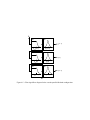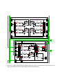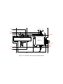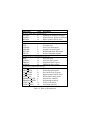
1
The BioSonar Front-end Signal Processor System Manual R. Timothy Edwards Johns Hopkins University Applied Physics Lab 11100 Johns Hopkins Road Laurel, MD 20723-6099 USA email: [email protected] December 28, 2001 Chapter 1 Introduction Certain animals such as bats and dolphins generate sonar signals (chirps or clicks) for the purpose of echolocation and object detection and classification. “Biomimetic sonar” refers to electrically-generated sonar signals designed to match the properties of the biologically-generated sonar signals. A biomimetic sonar signal processing system attempts to electronically mimic neural processing. This may be for the purpose of biological modeling, or for performing a task such as object recognition. Figure 1.1: Bottlenose dolphin. The Biomimetic Sonar Front-end Signal Processor System (generally referred to in this manual as the “BioSonar Processor”) was designed as a board-level system to investigate architectures for a (future) singlechip integrated biosonar signal processor. At the same time, however, the system is a functional analog signal processing system, capable of performing basic tasks associated with biological cochlear processing, including gain control, filtering through parallel bandpass functions, signal rectification, amplitude envelope extraction, and zero crossing detection. The system was designed using the latest commercial programmable analog and digital technology to make the system architecture flexible. The board relies on In-System Programmable (“ISP”) circuits such that the system architecture may be reconfigured on the fly from an external controller (such as a computer with a digital I/O interface). However, the ISP circuits use nonvolatile memory to store configuration information, so the biosonar front-end board retains its configuration when powered off, and may be programmed to operate independently of any external controller. 3 Chapter 2 System Overview Figure 2.1 shows the system setup as currently expected by the driver program. In this configuration, the board processes digital signals downloaded from the host computer. Main components of the system are as listed below: A Host computer, Intel or equivalent, running Linux. B Digital I/O card, PCI-DIO48, CIO-DIO48, or equivalent. C Bidirectional FIFO buffer board D BioSonar frontend processor E DC Power supply capable of delivering 1.2 A at 5 V. Because the host computer is using a non-real-time operating system (Linux), and also because the 82C55-based digital I/O card cannot keep up with the data rate of the biosonar processor, a bidirectional FIFO must be placed between the computer and the biosonar board. When real-time analog input is available to the board, and the board output directly drives a real-time back-end processor, the bidirectional FIFO buffer is not needed. That situation also allows the board to be configured to run without any connection to the computer; the digital interface is then used for new configuration downloads only. 50-pin ribbon cable and connectors E 5 V power supply @ 1.2 A B PCI-DIO48 or equivalent C A bidirectional FIFO buffer PC running Linux D biosonar signal processing board Figure 2.1: Biosonar Signal Processor: System-level diagram. Figure 2.2 is a depiction of the BioSonar frontend processor board. The board contains a filterbank of 34 channels implemented by Lattice ispPAC programmable analog arrays (one ispPAC-10 and one ispPAC-20 5 for each filter), one ispPAC-20 chip acting as a preamplifier with digital or analog input selectable, four Maxim MAX1202 12-bit analog-to-digital converter chips, a Lattice ispLSI-6192FF field-programmable gate array (FPGA) chip acting as an I/O interface, and a 20 MHz clock to drive the system. The ispPAC chips contain continuous-time biquad filter sections programmable in a range of 10 kHz to approximately 150 kHz, depending on the programmed value and input gain selection. This is contrary to the indications of the Lattice documentation, which declares the upper limit to be 100 kHz. The continuous-time nature of the chips also means that the preamplifier is not subject to the Nyquist frequency of the digital input, as would a digital or discrete-time filter. Power Ground PREAMP Lattice ispPAC20 1JI A009B02 ispPAC20 1JI A009B02 Lattice Lattice ispPAC20 1JI A009B02 ispPAC20 1JI A009B02 Lattice Lattice Lattice ispPAC20 1JI A009B02 Lattice ispPAC20 1JI A009B02 Lattice ispPAC20 1JI A009B02 ispPAC10 1PI A007D01 L ispPAC10 1PI A007D01 L ispPAC10 1PI A007D01 L ispPAC20 1JI A009B02 ispPAC10 1PI A007D01 L ispPAC10 1PI A007D01 L ispPAC10 1PI A007D01 L Lattice ispPAC20 1JI A009B02 Lattice ispPAC20 1JI A009B02 Lattice ispPAC20 1JI A009B02 Lattice ispPAC20 1JI A009B02 Lattice ispPAC20 1JI A009B02 Lattice ispPAC20 1JI A009B02 Lattice ispPAC20 1JI A009B02 Lattice ispPAC20 1JI A009B02 ispPAC10 1PI A007D01 L ispPAC10 1PI A007D01 ispPAC10 1PI A007D01 ispPAC10 1PI A007D01 L L L ispPAC10 1PI A007D01 ispPAC10 1PI A007D01 L L ispPAC10 1PI A007D01 ispPAC10 1PI A007D01 L L ispPAC10 1PI A007D01 ispPAC10 1PI A007D01 L L ispPAC10 1PI A007D01 ispPAC10 1PI A007D01 L L ispPAC10 1PI A007D01 Lattice L Lattice ispPAC10 1PI A007D01 Lattice L Lattice ispPAC10 1PI A007D01 Lattice L Lattice ispPAC10 1PI A007D01 Lattice L Lattice ispPAC20 1JI A009B02 ispPAC10 1PI A007D01 ispPAC20 1JI A009B02 L ispPAC20 1JI A009B02 ispPAC10 1PI A007D01 ispPAC20 1JI A009B02 L ispPAC20 1JI A009B02 ispPAC10 1PI A007D01 ispPAC20 1JI A009B02 L ispPAC20 1JI A009B02 ispPAC10 1PI A007D01 ispPAC20 1JI A009B02 L ispPAC10 1PI A007D01 ispPAC10 1PI A007D01 Lattice ispPAC10 1PI A007D01 Lattice ispPAC20 1JI A009B02 L Lattice ispPAC20 1JI A009B02 ispPAC10 1PI A007D01 Lattice ispPAC20 1JI A009B02 L Lattice ispPAC20 1JI A009B02 ispPAC10 1PI A007D01 Lattice ispPAC20 1JI A009B02 L Lattice ispPAC20 1JI A009B02 ispPAC10 1PI A007D01 Lattice ispPAC20 1JI A009B02 L Lattice ispPAC20 1JI A009B02 MAXIM MAX1202BCPP 0038 L L ispPAC10 1PI A007D01 ispPAC20 1JI A009B02 MAXIM MAX1202BCPP 0038 ispPAC10 1PI A007D01 L Lattice ispPAC20 1JI A009B02 MAXIM MAX1202BCPP 0038 20.0 M Lattice ispPAC20 1JI A009B02 Lattice MAXIM MAX1202BCPP 0038 ispLSI6192FF 50LM B921M01 J1 LM7805 J2A ext bias J2B J3A int bias J3B J4 analog in L 5V unregulated 5V regulated Figure 2.2: Biosonar Signal Processor: Frontend circuit board. The signal-level block diagram of the frontend board, indicating its major components, is shown in Figure 2.3. clock digital outputs analog outputs (serial) 34 32 MAX1202 × 4 34 7 38 SIN CS, SCLK, DIN,… ispLSI 6192FF 3 23 dedicated JTAG chain undedicated 16 analog input 4 8 data ispPAC20 TDO I/O #2 filter channel × 34 TDI I/O #1 control 8 ext. analog inputs 4 2 ... power supply +5 V,GND Analog I/O Figure 2.3: Biosonar Signal Processor: Block diagram of the frontend filterbank. Chapter 3 Hardware 3.1 Jumpered power supply and input configuration Figure 3.2 shows jumper settings on the biosonar board which are the only configuration options on the board that cannot be set remotely. In addition to the jumpers, the figure shows two of the three input connectors (the 50-pin digital I/O header socket is to the right of the figure and is not shown). All pins are pitched at 0.1 in spacing. The connector labeled “Power” and “Ground” is the main power input. The connector labeled “analog in” is the sonar signal input (microphone) when analog input is selected. Power supply options are selected by jumper , while signal input options are selected by jumpers , , and , and also by the programmed setting of the preamplifier. Jumper configurations are described below. Power modes are shown in Table 3.1 and described below: J1 top top bottom LM7805 uninstalled installed installed Mode A A B Table 3.1: Jumper configuration for input modes. ‘top’ indicates that the two pins closest to the top of the board are connected together, and the bottom pin is unconnected. ‘bottom’ indicates that the bottom two pins are connected together and the top pin is unconnected. A Connect the top two pins of for unregulated input. For this setting, power must be supplied by a regulated power supply (‘unregulated’ means that the biosonar board is not doing the regulation). ‘Power’ must be 5 V and ‘Ground’ must be 0 V. The supply must be able to deliver a sustained DC current of at least 1.2 A at 5 V. Because most of the chips contain continuous-time analog circuits, power consumption is fairly constant. B Connect the bottom two pins of for regulated input. For this setting, an LM7805 5 V regulator must be installed in the indicated position on the board. ‘Power’ must clear the dropout voltage of the regulator, which usually means about 8 V. Input modes are shown in Table 3.1 and described below. Figure 3.1 shows the bias circuit between the input pins and the preamplifier. A Differential signal goes directly from input pins to the ‘In1’ input of the preamplifer, buffered through 5 kΩ resistors. Differential input must be biased around 2.5 V. 9 J2A J3A J3B J4 5.0 kΩ 5.0 kΩ J2B 5.0 kΩ 5.0 kΩ − analog input + 2 15 16 8 9 ispPAC20 preamp Vrefout (2.5 V) In2+ In2− In1− In1+ Figure 3.1: Analog input circuit and configuration jumpers. J2A J2B X X J3A J3B X X X X X X X X X X X X J4 X X X X X X Mode A B C D E F G H J Table 3.2: Jumper configuration for input modes. An ‘X’ indicates that a jumper bridges the two pins (closed connection). No marking indicates an open connection. B Differential signal goes directly from input pins to the ‘In1’ input of the preamplifier with no buffering of any kind. Differential input must be biased around 2.5 V. C Differential signal goes from input pins to the ‘In1’ input of the preamplifier. Signal is rebiased to operate at or close to the preamplifer’s reference voltage of 2.5 V. D Single-ended signal goes directly from input ‘ ! ’ pin to the ‘In2! ’ input of the preamplifier, with no buffering. The single-ended input is assumed to be biased to always remain above ground (preferably around 2.5 V). E Single-ended signal goes from input ‘ ! ’ pin to the ‘In2! ’ input of the preamplifier, buffered by a 5 kΩ resistor. Bias requirements are the same as mode ‘D’ above. F Single-ended signal goes from input ‘ ! ’ pin to the ‘In2! ’ input of the preamplifier. Signal is rebiased to operate at or closed to the preamplifier’s reference voltage of 2.5 V. G Like mode ‘D’ above, but input ‘ " ’ pin is held at the reference voltage. H Like mode ’E’ above, but input ‘ " ’ pin is held at the reference voltage. J Like mode ’F’ above, but input ‘ " ’ pin is held at the reference voltage. 5V unregulated 5V regulated analog in Power Ground J1 LM7805 J2A ext bias J2B J3A int bias J3B J4 Figure 3.2: Biosonar Signal Processor: Frontend board configuration jumpers. Chapter 4 Firmware Much of the BioSonar system’s novelty lies in its ability to reconfigure its architecture through nonvolatile, re-writable configuration memory in the filter and interface chips. For the analog chips, filter frequency, filter resonance ( ), and filter type (lowpass, bandpass, highpass) are all programmable, and inputs may be selected from a number of different sources. In addition, the ispPAC20 features two comparators with selectable inputs, and an 8-bit DAC. The ispLSI6192-FF is a full-featured FPGA with general-purpose logic resources. The signal routing on the BioSonar printed circuit board is designed to allow several large-scale filterbank architectures, as well as letting the FPGA handle all routing between the board and any external computer or back-end processor. 4.1 The ISP JTAG protocol Four I/O pins on the 50-pin connector are dedicated to the ISP JTAG chain. JTAG is a protocol designed to allow boundary scans of programmable chips. Lattice Semiconductor makes dual use of the JTAG protocol to do both the boundary scan and also handle device configuration on the ispLSI-series chips. The ispPAC analog chips have no equivalent boundary scan capability, but they use the JTAG protocol for device configuration. The BioSonar system is intended to hide the details of the JTAG protocol from the end-user; these protocols are embedded in the software but the end-user is intended to use higher-level calls to erase, program, and verify the devices. However, some details of the JTAG architecture elucidate the use of the software subroutines. JTAG is a serial protocol, requiring for each chip two data bit lines (TDI and TDO), plus one mode bit (TMS) and one clock signal (TCK). A well-defined state machine, called the TAP controller and shown in Figure 4.1, allows 5-bit commands, some of which are defined by the protocol, such as “BYPASS” to form a one-bit link between TDI and TDO which bypasses the chip. Lattice defines other commands such as “ERASE,” “PROGRAM,” and “VERIFY.” All chips on the board form one long serial JTAG chain by linking TDO of one chip to TDI of the next chip in the chain, and supplying TMS and TCK to all chips in parallel. The chain, in order, is shown in red in Figure 4.2. While it is convenient to think of the JTAG chain as a single, very long configuration word, in reality the ispLSI chip must be programmed differently, by supplying 180 separate bit streams, addressed by a different bit. So the actual programming for the board is done in two stages, one for the ispLSI, and one for all of the ispPAC chips. During each stage, the set of chips not being accessed are placed into BYPASS mode. In addition to being programmed in a different manner, the ispLSI chip is a general-purpose FPGA which requires complicated placement and routing to program. Because the placement and routing algorithms, and the purpose of each configuration bit is Lattice proprietary information, the ispLSI chip must be designed in Lattice software, outside of the BioSonar system, producing a “JDEC” file containing the configuration bit stream for the ispLSI. The purpose of each configuration bit in the ispPAC chips is known, so 13 1 $0 $0 Test-Logic-Reset Run-Test/Idle 1 $0 Select-DR-Scan 1 $0 1 1 Capture-DR $0 #Shift-IR 1 $0 Pause-DR 1 Exit2-DR $0 1 $0 Exit1-IR $0 Pause-IR $0 1 Exit2-IR 1 1 $0 Update-DR 1 $0 1 1 Exit1-DR 1 Capture-IR $0 Shift-DR $0 $0 Select-IR-Scan $0 Update-IR 1 Figure 4.1: The JTAG Test Access Port (“TAP”) state machine. Bit values shown represent the state of signal TMS at the time of a rising edge of signal TCK. all configuration can be determined on the fly by the BioSonar system software (see the section on software). 4.2 The ispLSI-6192FF I/O Interface The ispLSI-6192FF device is a 207-pin surface-mount device, running at 5 V, containing nonvolatile EEPROM configuration memory, and implementing a JTAG interface compatible with the ispPAC devices. On the biosonar board, the ispLSI chip has been mounted on top of a surface-mount-to-PGA converter board, and plugged into a 17 % 17 PGA socket. Unfortunately, Lattice Semiconductor has discontinued the ispLSI-6192FF device (the entire 6000 series has been discontinued), and even more unfortunately, they have made the poor decision to discontinue software support for the device, as well. Although the Lattice Semiconductor software is freely distributed, recent versions of the program will not compile schematics for the 6192 device. The only option is to continue to use an older version of the Lattice “ispDesignExpert” software (version 8.0). A copy of this software version is included with the software package for the BioSonar frontend board. A software license is freely available from Lattice Semiconductor (http://www.latticesemi.com), but must be obtained before the software can be used. In the provided software, the schematic layout corresponding to the latest BioSonar board revision can be found in directory Lattice & Biosonar & . The “project” is the file biosonar.syn and is configured to launch the ispDesign Expert Project Manager program upon selection. The schematic for the BioSonar interface (assuming a FIFO board) is drawn in Figure 4.4. Altering the interface requires understanding the interface, so a brief description follows. Two main circuits in the schematic, FIFO4 and T4R4CPV, are hardwired circuits on the ispLSI6192FF. The T4R4CPV is one of several possible configurations of the on-board register bank. This particular configuration treats the register bank as four 16-bit up-down counters and four 16-bit registers. Each register/counter has its own clock signal, and each counter provides a “terminal count” output (B' TC). Three “select” pins (BS0–BS2) select which register receives input from bus DI and applies its value to output bus in Power Ground 5V unregulated 5V regulated out J1 PREAMP Lattice ispPAC20 1JI A009B02 ispPAC20 1JI A009B02 Lattice Lattice ispPAC20 1JI A009B02 ispPAC20 1JI A009B02 Lattice Lattice Lattice ispPAC20 1JI A009B02 Lattice ispPAC20 1JI A009B02 Lattice ispPAC20 1JI A009B02 ispPAC10 1PI A007D01 L ispPAC10 1PI A007D01 L ispPAC10 1PI A007D01 L ispPAC20 1JI A009B02 ispPAC10 1PI A007D01 L ispPAC10 1PI A007D01 L ispPAC10 1PI A007D01 L Lattice ispPAC20 1JI A009B02 Lattice ispPAC20 1JI A009B02 Lattice ispPAC20 1JI A009B02 Lattice ispPAC20 1JI A009B02 Lattice ispPAC20 1JI A009B02 Lattice ispPAC20 1JI A009B02 Lattice ispPAC20 1JI A009B02 Lattice ispPAC20 1JI A009B02 ispPAC10 1PI A007D01 L ispPAC10 1PI A007D01 ispPAC10 1PI A007D01 ispPAC10 1PI A007D01 L L L ispPAC10 1PI A007D01 ispPAC10 1PI A007D01 L L ispPAC10 1PI A007D01 ispPAC10 1PI A007D01 L L ispPAC10 1PI A007D01 ispPAC10 1PI A007D01 L L ispPAC10 1PI A007D01 ispPAC10 1PI A007D01 L L ispPAC10 1PI A007D01 Lattice L Lattice ispPAC10 1PI A007D01 Lattice L Lattice ispPAC10 1PI A007D01 Lattice L Lattice ispPAC10 1PI A007D01 Lattice L Lattice ispPAC20 1JI A009B02 ispPAC10 1PI A007D01 ispPAC20 1JI A009B02 L ispPAC20 1JI A009B02 ispPAC10 1PI A007D01 ispPAC20 1JI A009B02 L ispPAC20 1JI A009B02 ispPAC10 1PI A007D01 ispPAC20 1JI A009B02 L ispPAC20 1JI A009B02 ispPAC10 1PI A007D01 ispPAC20 1JI A009B02 L ispPAC10 1PI A007D01 ispPAC10 1PI A007D01 Lattice ispPAC10 1PI A007D01 Lattice ispPAC20 1JI A009B02 L Lattice ispPAC20 1JI A009B02 ispPAC10 1PI A007D01 Lattice ispPAC20 1JI A009B02 L Lattice ispPAC20 1JI A009B02 ispPAC10 1PI A007D01 Lattice ispPAC20 1JI A009B02 L Lattice ispPAC20 1JI A009B02 ispPAC10 1PI A007D01 Lattice ispPAC20 1JI A009B02 L Lattice ispPAC20 1JI A009B02 MAXIM MAX1202BCPP 0038 L L ispPAC10 1PI A007D01 ispPAC20 1JI A009B02 MAXIM MAX1202BCPP 0038 ispPAC10 1PI A007D01 L Lattice ispPAC20 1JI A009B02 MAXIM MAX1202BCPP 0038 20.0 M Lattice ispPAC20 1JI A009B02 Lattice MAXIM MAX1202BCPP 0038 ispLSI6192FF 50LM B921M01 LM7805 J2A ext bias J2B J3A int bias J3B J4 L analog in Figure 4.2: The JTAG serial chain links every chip on the board into one long serial bit stream. DO. The T4R4CPV defines a preset bit sequence for each counter which is loaded on “enable” (B' PLEN) for that counter (')(+*,.-/0-/10-32,4 ). The preset value can be set by editing the T4R4CPV schematic and changing the appropriate inputs. Figure 4.5 shows how the preset values are specified in the ispDesignExpert software: Each bit is determined by the connection of the preset value block’s input to either Vdd or GND, to denote a preset value of 1 or 0. No other schematic connections to the inputs are valid. Similarly, the CAOCTRL block indicates the polarity of the carry-out bit of the counter, and the POLCTRL block indicates the polarity of the EN enable bit of the T4R4CPV module. In the BioSonar system application, the four registers of the T4R4CPV are not used, and the counters are used to divide down the input 20 MHz clock into several different frequencies required by the BioSonar system. Note in particular that the BioSonar board’s input and output operate independently; therefore, input- and output-handling circuits are clocked at separate rates. The circuit uses two of the 5 dedicated clock inputs on the ispLSI6192FF for these two rates. The slower clock input is generated by the ispLSI6192 circuit. However, because the ispLSI clock networks are fixed, it is necessary to put the divided-down clock (signal CLK OUT) on an ispLSI6192 output pin, and route the output back to the second clock input via the printed circuit board. Each counters “terminal count” output is fed directly back to the “enable” input, Figure 4.3: ispDesignExpert project manager window. resetint PS D0 Vdd Q0 D0 CS 54 N/C MIN[8] 43 N/C MIN[9] 45 N/C MIN[10] 84 N/C resetint MIN[7] 5 5 204 206 203 189 199 6 200 193 82 N/C MIN[12] 80 N/C MIN[13] MIN[14] 79 86 BWRL ARDL MRST NCSpmp 88 62 Q0 D0 Q0 D0 Q0 5 D0 CD CD ALE ALF EF FF FIFO4 clkint N/C MOUT[7] 207 N/C CD 60 PCpmp 55 ENSPIpmp 58 MSELpmp ALE ADO[8:0] BDI[8:0] MIN[11] 17 DO[2] DO[1] 184 ADCSSTRB FIFOWR DO[7] DO[6] DO[5] DO[4] DO[3] 124 125 127 129 130 131 132 133 134 FDI8 N/C FDI7 N/C 47 FDI5 48 MIN[6] FDI6 MIN[5] FDI3 N/C CS FDI4 N/C 52 CS FDI1 51 MIN[4] CS FDI2 MIN[3] CS FDI0 N/C FDO0 clk2int 53 MIN[2] 194 Q0 Q0 FDO7 D0 FDO8 Q0 FDO6 D0 D0 FDO5 Q0 PS Q0 clk2int PS FDO3 D0 PS FDO4 Q0 PS FDO2 D0 PS FDO1 PS 37 ALF 83 EF 41 FF 14 MOUT[8] 12 MOUT[9] 9 MOUT[10] 7 MOUT[11] 18 MOUT[12] 1 MOUT[13] 16 MOUT[14] 8 MOUT[15] 38 MOUT[0] 33 MOUT[1] 34 MOUT[2] 36 MOUT[3] 32 MOUT[4] 20 MOUT[5] 19 MOUT[6] 64 ADCDOUT[0] 68 ADCDOUT[1] 90 ADCDOUT[2] 175 ADCDOUT[3] FWR DO[0] N/C DO[1] MIN[15] 69 N/C MIN[16] 66 N/C FIFORD 67 G LD14 RST MIN[17] 196 4 resetint N/C ADCCSBAR 188 MIN[18] 96 N/C MIN[19] 97 N/C MIN[20] 95 N/C MIN[21] 94 N/C DI[15:0] MIN[22] 92 N/C MIN[23] 89 N/C MIN[24] 87 N/C MIN[25] 85 N/C MIN[26] 181 N/C MIN[27] 177 N/C MIN[28] 176 N/C MIN[29] 172 N/C MIN[30] 171 N/C B1PLEN B3PLEN B5PLEN B7PLEN B1SZ B3SZ B5SZ B7SZ BS0 T4R4CPV BS1 B1TC BS2 B3TC B1UD B5TC B3UD B7TC B5UD B7UD DO[15:0] B1CH B3CH B5CH B7CH MIN[31] 170 N/C MIN[32] 169 N/C MIN[33] 173 N/C 63 DMODEpmp D0 Q0 186 count1out D1 D2 D3 Q1 Q2 Q3 MRST Vdd CLK_IN CLK2_IN 24 78 clkint clk2int B0CLK B1CLK B2CLK B3CLK B4CLK B5CLK B6CLK B7CLK 183 CLK_OUT 198 STROBE 182 DO[6] DO[7] A0 DO[5] A1 A2 A3 Z0 DO[1] DO[2] S0 S1 ADCIN Vdd MUX4 6 A0 A1 Z0 MUX2 S0 SELECT0 10 65 ENSPIflt SELECT1 205 192 MSELflt Calibrate 40 190 CALflt DO[3] N/C DO[4] EN DO[0] 179 SCLK Figure 4.4: Schematic drawing of the interface circuit. This schematic corresponds to the JEDEC file “expt.jed”. DI[0:15] B1PLEN B3PLEN B5PLEN B7PLEN B1SZ B3SZ B5SZ B7SZ BS0 BS1 BS2 DO[0:15] DO[0:15] B1PLEN B3PLEN B5PLEN B7PLEN B1SZ B3SZ B5SZ B7SZ BS0 BS1 BS2 B1UD B3UD B5UD B7UD B1UD B3UD B5UD B7UD B1CH B3CH B5CH B7CH B1CH B3CH B5CH B7CH B0CLK B1CLK B2CLK B3CLK B4CLK B5CLK B6CLK B7CLK Vdd DI[0:15] B0CLK B1CLK B2CLK B3CLK B4CLK B5CLK B6CLK B7CLK POLCTRL POLIN0 POL0 POLEN CAOCTRBK1 BK_IN BK_CAOCTRL RP1 CAOCTRBK3 BK_IN BK_CAOCTRL RP3 CAOCTRBK5 BK_IN BK_CAOCTRL RP5 CAOCTRBK7 BK_IN BK_CAOCTRL RP7 PSI15 PSI14 PSI13 PSI12 PSI11 PSI10 PSI9 PSI8 CPVBK7 PSI7 PSI6 PSI5 PSI4 PSI3 PSI2 PSI1 PSI0 PSO15 PSO14 PSO13 PSO12 PSO11 PSO10 PSO9 PSO8 PSO7 PSO6 PSO5 PSO4 PSO3 PSO2 PSO1 PSO0 CPV7_15 CPV7_14 CPV7_13 CPV7_12 CPV7_11 CPV7_10 CPV7_9 CPV7_8 CPV7_7 CPV7_6 CPV7_5 CPV7_4 CPV7_3 CPV7_2 CPV7_1 CPV7_0 PSI15 PSI14 PSI13 PSI12 PSI11 PSI10 PSI9 PSI8 CPVBK5 PSI7 PSI6 PSI5 PSI4 PSI3 PSI2 PSI1 PSI0 PSO15 PSO14 PSO13 PSO12 PSO11 PSO10 PSO9 PSO8 PSO7 PSO6 PSO5 PSO4 PSO3 PSO2 PSO1 PSO0 CPV5_15 CPV5_14 CPV5_13 CPV5_12 CPV5_11 CPV5_10 CPV5_9 CPV5_8 CPV5_7 CPV5_6 CPV5_5 CPV5_4 CPV5_3 CPV5_2 CPV5_1 CPV5_0 PSI15 PSI14 PSI13 PSI12 PSI11 PSI10 PSI9 PSI8 CPVBK3 PSI7 PSI6 PSI5 PSI4 PSI3 PSI2 PSI1 PSI0 PSO15 PSO14 PSO13 PSO12 PSO11 PSO10 PSO9 PSO8 PSO7 PSO6 PSO5 PSO4 PSO3 PSO2 PSO1 PSO0 CPV3_15 CPV3_14 CPV3_13 CPV3_12 CPV3_11 CPV3_10 CPV3_9 CPV3_8 CPV3_7 CPV3_6 CPV3_5 CPV3_4 CPV3_3 CPV3_2 CPV3_1 CPV3_0 PSI15 PSI14 PSI13 PSI12 PSI11 PSI10 PSI9 PSI8 CPVBK1 PSI7 PSI6 PSI5 PSI4 PSI3 PSI2 PSI1 PSI0 PSO15 PSO14 PSO13 PSO12 PSO11 PSO10 PSO9 PSO8 PSO7 PSO6 PSO5 PSO4 PSO3 PSO2 PSO1 PSO0 CPV1_15 CPV1_14 CPV1_13 CPV1_12 CPV1_11 CPV1_10 CPV1_9 CPV1_8 CPV1_7 CPV1_6 CPV1_5 CPV1_4 CPV1_3 CPV1_2 CPV1_1 CPV1_0 7 TR4CPV B1TC B3TC B5TC B7TC B1TC B3TC B5TC B7TC EN EN Figure 4.5: Schematic of the T4R4CPV register/counter module, showing register preset value programming. forming a continuous output. The “select” pins are grounded to enable the continuous monitoring of the value of the first counter on the DO output bus. Mux logic generates various internal and external event signals based on the value of the primary counter’s instantaneous value. The preset values for the four counters, as indicated in Figure 4.5, are: counter 1 3 5 7 bit value 0000000001001110 0000011111010000 0000000000000101 0000000100000000 hex value 0x004e 0x07d0 0x0005 0x0100 decimal value 78 2000 5 256 time 3.9 µs 100 µs 0.25 µs 64 µs frequency 256 kHz 10 kHz 4 MHz 15.625 kHz Table 4.1: Default timer values programmed into the interface. Time and frequency values are measured assuming an input master clock rate of 20 MHz for counters 1, 3, and 5, and assuming that the output of counter 5 becomes the input to counter 7 (connection must be made off-chip). The FIFO module is effectively replaced by the external bidirectional FIFO board. The arrangement of the BioSonar board requires that the FIFO be put in the “FIFO4” configuration, in which it acts as an input buffer between the I/O connector and the preamplifier’s DAC inputs, and has a size of 9-bit words % 8192 locations. Because the FIFO outputs are hard-wired to specific pins on the ispLSI6192, the FIFO cannot be removed from the system. For use with the external FIFO board, however, it must be bypassed. This is accomplished with a timed sequence of signals to the FIFO’s “read” (ARDL) and “write” (BWRL) inputs, ensuring that the FIFO4 module does exactly one write and one read operation in sequence for every input retrieved from the external FIFO board. The external board is queried by the FIFORD signal. In addition to clock frequency division and input retrieval, the ispLSI6192 interface is responsible for collecting outputs from the BioSonar frontend. There are two separate outputs available from each filterbank channel. One is a single-bit digital output, and one is an analog value. The nature of the output depends on the configuration of the analog filterbank chips (see below). Each of the 34 digital outputs is connected directly to ispLSI6192 inputs. The present schematic does not make use of the digital outputs, so they are shown as not connected. The analog outputs feed to four Maxim MAX1202 ADC chips, each with eight multiplexed inputs (so there are 32 analog outputs available for 34 channels; the analog output of the two highest-frequency channels cannot be accessed, although the digital output is available). The ispLSI6192 is responsible for generating the signals that driver the Maxim chips. ADCIN is the serial bit stream containing configuration information for the ADC chip. SCLK clocks the ADC. The ADC configuration is an 8-bit word, described in the Maxim MAX1202 data sheet, and summarized in Table 4.2: Bit 7 6 5 4 3 2 1 0 Name START SEL2 SEL1 SEL0 UNI/8:9 SGL/ ;=<?> PD1 PD0 Description First bit defines beginning of control byte. Select which channel is read. Numerically, Channel (0–7) = Sel1 (MSB), Sel0, Sel2 (LSB) 1 = unipolar (always) 1 = single ended (always) Power-down mode and clock select PD1 = 1, PD0 = 1 External clock mode (always) Table 4.2: Bit values of the Maxim MAX1202 configuration word. All ADC configuration bits are ‘1’ except for the channel selection. The Mux logic provided by the “MUX4” and “MUX2” gates inserts the proper channel number such that each channel is accessed in se- @quence. ADCSSTRB indicates a completed ADC output, and is used in this schematic to drive the output. FIFOWR is derived directly from the ADCSSTRB signal. The ADC output is 12 bits long and read out serially. Each of the four ADC chips provides a separate output bit stream. The ADC clock (SCLK) has a maximum rate of 2 MHz and the time for an ADC conversion is 16 clocks (the minimum possible time for a conversion is 15 clocks, but the convenience of generating signals based on a cycle of 16 outweighs the advantage of a slightly faster conversion). So the minimum possible time to capture all 32 analog outputs is %FHGBIKJLINMPOHQR%TSBI/UWVYXZX[OHM\Q](^G_ BADC=E µs which is an output rate of 15.625 kHz. No attempt should be made to set the output rate (counter) to a cycle frequency greater than this number. It represents the maximum rate at which analog data can be extracted from the BioSonar board. This is the default rate programmed into the output counter as shown in Table 4.1. Each cycle of output sampling produces Ha`cbPdeQf%gYBI/UWVYXZX[OHM\Qh(iYS_`Wb\deQ output. However, in this circuit instantiation, output is generated at the fastest rate using the simplest possible method, in which no attempt is made to organize the output into meaningful words. Instead, the 8 lowest bits of the 9-bit output FIFO are loaded 4 bits at a time with the 4 ADC outputs. The FIFO is written every two clock cycles of the ADC clock. On the first ADC clock, the ADC output is latched into the upper four bits of the FIFO word. On the second ADC clock, the ADC output is directed to the lower four bits of the FIFO word, and all 8 bits are written into the FIFO. After all 12 bits are loaded into the FIFO, the ADC receives configuration information for the next input channel, and the cycle repeats until all 8 channels have been read, converted, and transferred to the output FIFO. In the current instantiation, it is the reponsibility of the back-end system to translate this bit block back into meaningful values, and, if necessary, sort the channels into their sequence in the filterbank. Because the FIFO has 9 bits, the 9th bit is used to generate a synchronization bit which indicates to the back-end system that a block of data is beginning. This synchronization bit is sent coincident with the first byte written to the FIFO. On the schematic drawing, each input or output pad contains the number corresponding to the ispLSI pin to which it is attached. Pin numbers and signal names are fixed according to the BioSonar printed circuit board. However, internal signals and all routing are determined by the Lattice ispDesignExpert placement and routing algorithms. The goal of compiling the circuit in ispDesignExpert is to generate a “JDEC” file containing the configuration bits for the ispLSI6192FF. This file, which has the extension ‘.jed’, is transferred from the Windows machine used to run the ispDesignExpert software to the Linux machine running the BioSonar board application (see below). The application program accepts the file exactly as written by ispDesignExpert. Tables 4.3 through 4.6 give a complete list of pins on the ispLSI6192FF, their signal names as relevant to the BioSonar board, and a description of each signal. The first pin number is for the ispLSI6192FF quad flat pack package, for use in assigning signals to pins in the ispDesignExpert program. The second pin number is the corresponding pin grid array (PGA) pin number, for the purpose of probing signals on the BioSonar frontend circuit board. DIO pin numbers are for the CIO-DIO96 or PCI-DIO96 50-pin connectors, with names corresponding to the BioSonar system software (CIO-DIO96 driver software and filterbank application program). All of the signal names in the table correspond to signal names on the schematic, except for signals which are hardwired to the ispLSI6192FF for the purpose of JTAG programming and are therefore not available as inputs and outputs. These include TDI, TDO, TCK, TMS, BSCAN, and !RST. Pins labeled Y1 and Y2 are dedicated clock network inputs, and pins labeled FIFO ' are dedicated FIFO outputs. Because the FIFO pins are hardwired to the preamplifier DAC inputs on the BioSonar circuit board, the FIFO is required to operate pin 8 16 1 18 7 9 12 14 17 19 20 32 36 34 33 38 200 6 199 189 203 206 204 5 88 37 83 41 196 194 136 29 28 99 26 72 198 205 10 207 4 40 PGA C1 F2 D3 F1 E4 F3 F4 G3 G4 H3 G2 K2 L4 L3 L1 M2 C5 C2 A4 A7 A3 A2 B3 B1 P11 M1 P10 M4 A5 B6 H16 K3 J2 S15 J4 R7 B5 C4 D2 D4 E3 N1 ispLSI name I/O 85 I/O 91 I/O 79 I/O 93 I/O 84 I/O 86 I/O 88 I/O 89 I/O 92 I/O 94 I/O 95 I/O 0 I/O 3 I/O 2 I/O 1 I/O 5 I/O 72 I/O 83 I/O 71 I/O 64 I/O 74 I/O 77 I/O 75 I/O 82 I/O 40 I/O 4 I/O 35 I/O 7 I/O 69 I/O 68 TDO TMS TCLK !RST BSCAN TOE I/O 70 I/O 76 I/O 87 I/O 78 I/O 81 I/O 6 signal name MOUT[15] MOUT[14] MOUT[13] MOUT[12] MOUT[11] MOUT[10] MOUT[9] MOUT[8] MOUT[7] MOUT[6] MOUT[5] MOUT[4] MOUT[3] MOUT[2] MOUT[1] MOUT[0] FDI7 FDI6 FDI5 FDI4 FDI3 FDI2 FDI1 FDI0 ALE ALF FE FF FIFORD FIFOWR TDO (JTAG out) TMS TCK !TRST BSCAN TOE STROBE SELECT1 SELECT0 FWR RST Calibrate description DIO (pin 25) DIO (pin 26) DIO (pin 27) DIO (pin 28) DIO (pin 29) DIO (pin 30) DIO (pin 31) DIO (pin 32) DIO (pin 33) DIO (pin 34) DIO (pin 35) DIO (pin 36) DIO (pin 37) DIO (pin 38) DIO (pin 39) DIO (pin 40) DIO (pin 9) DIO (pin 10) DIO (pin 11) DIO (pin 12) DIO (pin 13) DIO (pin 14) DIO (pin 15) DIO (pin 16) DIO (pin 41) DIO (pin 42) DIO (pin 43) DIO (pin 44) DIO (pin 5) DIO (pin 6) DIO (pin 4) DIO (pin 18) DIO (pin 46) DIO (pin 23) DIO (pin 24) DIO (pin 48) DIO (pin 8) DIO (pin 19) DIO (pin 20) DIO (pin 21) DIO (pin 22) DIO (pin 45) Table 4.3: Signals connecting the ispLSI6192FF interface chip to the digital I/O (DIO) 50-pin connector, and their corresponding pin numbers. pin 193 186 183 179 PGA A6 A8 A9 B10 ispLSI name I/O 67 I/O 61 I/O 59 I/O 56 signal name FDI8 count1Out CLK OUT SCLK description DIO (B) (pin 48) DIO (B) (pin 46) DIO (B) (pin 44) DIO (B) (pin 42) Table 4.4: Signals connecting the ispLSI6192FF interface chip to the auxiliary I/O (DIO) area, and the corresponding pin numbers. These pins are expected to be used to probe diagnostic signals; no physical header is connected to the board in this area. pin 27 64 68 90 175 188 184 187 182 24 78 190 192 65 55 58 60 62 63 124 125 127 129 130 131 132 133 134 44 49 201 15 PGA J1 P6 R6 R12 C10 B8 B9 D8 D9 J3 P9 C7 D7 R5 S1 R3 S3 R4 S4 L16 L17 K16 K17 J14 J17 J16 H15 H17 N3 P3 B4 E1 ispLSI name TDI I/O 26 I/O 30 I/O 42 I/O 53 I/O 63 I/O 60 I/O 62 I/O 58 Y1 Y2 I/O 65 I/O 66 I/O 27 I/O 19 I/O 21 I/O 22 I/O 24 I/O 25 FIFO 9 FIFO 10 FIFO 11 FIFO 12 FIFO 13 FIFO 14 FIFO 15 FIFO 16 FIFO 17 I/O 10 I/O 14 I/O 73 I/O 90 signal name TDI ADCDOUT[0] ADCDOUT[1] ADCDOUT[2] ADCDOUT[3] ADCCSBAR ADCSSTRB SCLK ADCIN CLK IN CLK2 IN CALflt MSELflt ENSPIflt ENSPIpmp MSELpmp PCpmp NCSpmp DMODEpmp FDO0 FDO1 FDO2 FDO3 FDO4 FDO5 FDO6 FDO7 (unconnected) (unconnected) (unconnected) (unconnected) (unconnected) description JTAG input from last filter ADC #1 (pin15) ADC #2 (pin15) ADC #3 (pin15) ADC #4 (pin15) !CS to all ADCs (pin 18) SSTRB from all ADCs (pin 16) SCLK to all ADCs (pin 19) DIN to all ADCs (pin 17) clock chip output connected to CLK OUT all ispPAC10 and 20 Calibrate filter ispPAC20 mux select filter ispPAC10 and 20 ENSPI preamp ENSPI (pin 4) preamp MSEL (pin 5) preamp PC (pin 21) preamp !CS (pin 22) preamp DMODE (pin 24) preamp DAC data in lsb (pin 32) preamp DAC data in (pin 33) preamp DAC data in (pin 34) preamp DAC data in (pin 35) preamp DAC data in (pin 36) preamp DAC data in (pin 37) preamp DAC data in (pin 38) preamp DAC data in msb (pin 39) Table 4.5: Signals connecting the ispLSI6192FF interface chip to the rest of the BioSonar frontend board, and their corresponding pin numbers. pin 61 56 53 51 52 48 47 54 43 45 84 82 80 79 86 69 66 67 96 97 95 94 92 89 87 85 181 177 176 172 171 170 169 173 PGA Q6 Q5 Q4 P4 R2 Q2 Q1 Q3 P1 P2 R10 S10 R9 S9 Q11 P7 Q7 S5 Q13 R14 S14 R13 S13 S12 R11 S11 A10 A11 B11 B12 A13 C11 B13 D11 ispLSI name I/O 23 I/O 20 I/O 17 I/O 15 I/O 16 I/O 13 I/O 12 I/O 18 I/O 9 I/O 11 I/O 36 I/O 34 I/O 33 I/O 32 I/O 38 I/O 31 I/O 28 I/O 29 I/O 46 I/O 47 I/O 45 I/O 44 I/O 43 I/O 41 I/O 39 I/O 37 I/O 57 I/O 55 I/O 54 I/O 51 I/O 50 I/O 49 I/O 48 I/O 52 signal name MIN[1] MIN[2] MIN[3] MIN[4] MIN[5] MIN[6] MIN[7] MIN[8] MIN[9] MIN[10] MIN[11] MIN[12] MIN[13] MIN[14] MIN[15] MIN[16] MIN[17] MIN[18] MIN[19] MIN[20] MIN[21] MIN[22] MIN[23] MIN[24] MIN[25] MIN[26] MIN[27] MIN[28] MIN[29] MIN[30] MIN[31] MIN[32] MIN[33] MIN[34] description filter channel 1 digital output filter channel 2 digital output filter channel 3 digital output filter channel 4 digital output filter channel 5 digital output filter channel 6 digital output filter channel 7 digital output filter channel 8 digital output filter channel 9 digital output filter channel 10 digital output filter channel 11 digital output filter channel 12 digital output filter channel 13 digital output filter channel 14 digital output filter channel 15 digital output filter channel 16 digital output filter channel 17 digital output filter channel 18 digital output filter channel 19 digital output filter channel 20 digital output filter channel 21 digital output filter channel 22 digital output filter channel 23 digital output filter channel 24 digital output filter channel 25 digital output filter channel 26 digital output filter channel 27 digital output filter channel 28 digital output filter channel 29 digital output filter channel 30 digital output filter channel 31 digital output filter channel 32 digital output filter channel 33 digital output filter channel 34 digital output Table 4.6: Signals connecting the ispLSI6192FF interface chip to the filterbank channel single-bit digital outputs, and their corresponding pin numbers. j in the mode in which these pins are used as FIFO outputs, not inputs. The pin marked “(unused)” was not required by the schematic, although it is available for general purpose output. Pins marked “(unconnected)” are the remaining general-purpose I/O on the ispLSI6192FF. These pins are unconnected due to board layout errors and cuts made for rewiring, and should not be used. k 4.3 The DIO Interface From the standpoint of any back-end hardware, the DIO interface is simply a collection of pins, most of which can be programmed either as input or output on the ispLSI-6192FF for any purpose whatsoever, but with a few pins reserved for use by the JTAG programming. Figure 4.6 shows the 50-pin connector. For use with arbitrary back-end hardware, Figure 4.6 (a) highlights which pins (corresponding to Figure 4.3) are available for general-purpose I/O through the ispLSI-6192 interface, and which pins are reserved for the JTAG interface and for power, and which pins have no connections. N/C N/C I/O_69 (196) N/C I/O_72 (200) |a v n31 o42 p w x75 y68 z9 10 b TDO I/O_68 (194) 11 12 I/O_64 (189) 13 14 I/O_77 (206) I/O_75 (204) 15 16 I/O_82 (5) q BP B, = input or output BP C = output only I/O_87 (10) I/O_81 (4) q qTRST v23 v24 BSCAN FIFO1,2 MR I/O_76 (205) BSCAN 19 ldata in I/O_86 (9) from FIFO I/O_89 (14) AP A, B, CH = input or output I/O_94 (19) I/O_0 (32) I/O_2 (34) I/O_5 (38) I/O_4 (37) mAP CL 45 46 TCK = output only o49 p50 rGND uSync bit n34 I/O_94 (19) n n I/O_95 (20) 35 36 I/O_0 (32) n n I/O_3 (36) 37 38 I/O_2 (34) n o q I/O_1 (33) 39 4 TDO o o q I/O_40 (88) 45 46 TCK qTDI 47 48 qTOE FIFO1 full FIFO1 empty FIFO2 full o p rFIFO2 empty sopen-circuit as seen from computer can be wired to unused output pins. tside; connection from computer into one of mA2 mA0 A 10 B6 B5 11 12 B4 13 14 B2 {C7 17 18 C6 B BP { mAP A, B= input mAP CH {C5 {C3 {C1 = output AP CL = input Vdd DIO pins on the biosonar board as seen from the computer (software) with the dual FIFO board in between. This corresponds to the “filterbank” program. Pin on biosonar board does not connect to any circuits. Reserved—Vdd Reserverd—JTAG interface Reserved—GND {C4 { { C v 19 20 21 22 v23 v24 v2725 v2628 v29 n30 n n n 31 n32 B7 33 34 n n B5 35 36 n n B3 37 38 n o {C7B1 39o41 o4042 Vdd 49 50 GND DIO pins on the biosonar board as seen from the computer (software) with a direct connection between the computer and the biosonar board (no FIFO board). mA4 B3 {C5 {C3 { mA7C1 mA5 mA3 mA1 FIFO2 RD I/O_93 (18) z9 mA6 B1 15 16 B0 FIFO1 WR I/O_91 (16) the FIFO buffer chips B7 I/O_81 (4) 22 18 TMS 17 18 TMS TDI 47 48 LSI TOE Vdd BP A, B, C = output 17 N/C I/O_35 (83) 43 44 I/O_7 (41) I/O_40 (88) to FIFO I/O_83 (6) I/O_74 (203) v I/O_76 (205) 19 20 I/O_78 (207) 21 22 v v TRST 23 24 I/O_85 (8) 25 26 v v I/O_79 (1) 27 28 v n I/O_84 (7) 29 30 n n I/O_88 (12) 31 32 n n I/O_92 (17) 33 34 n n I/O_95 (20) 35 36 n n I/O_3 (36) 37 38 n o I/O_1 (33) 39 40 o o I/O_40 (88) 41 42 BP A = input only I/O_70 (198) I/O_71 (199) N/C mA7 mA5 mA3 mA1 ldata out N/C }c v n31 o42 p5 w6 x7 y8 C2 {C0 mA6 mA4 mA2 mA0 A B6 B4 B2 {B0 C6 { { 43 44 C4 {C0 45 46 C2 B AP {C o4749 p4850 rGND DIO connector, 50 pin and 82C55 ports as arranged on the CIO-DIO48 card rGeneral-purpose I/O Figure 4.6: The DIO 50-pin interface (generic pin names). On the computer end of the system, the software driver program accesses the BioSonar board through the 50-pin connector at the input of the dual FIFO board. When the dual FIFO board is connected between the computer and the BioSonar board, many interface pins become reserved for use by the two FIFO chips (data lines and the FIFO read/write controls). Some of the remaining interface lines simply pass through the FIFO board unchanged. However, other lines are rearranged as they pass through the FIFO board to accomodate the vagaries of the 82C55 ports on the CIO-DIO48 interface to the computer. Figure 4.6 (b) shows what signals and ispLSI-6192FF general-purpose I/O pins can be addressed from software with the FIFO board in place. The numbering of the pins in this figure match the pin numbers on the BioSonar board, showing how the pins are rearranged by the wire-wrapped jumpers on the FIFO board. The software does not address the interface by pin number, however, but by reference to the two 82C55 interface chips and their ports (A, B, and C, 8 bits each). Figure 4.6 (c) maps the 82C55 ports of the CIO-DIO48 interface to the 50-pin connector. This mapping is reproduced from the Measurement Computing, Inc. (formerly ComputerBoards, Inc.) PCI-DIO96 Digital Input/Output User’s Manual (Rev. 2, Nov. 2000). The 82C55 ports are grouped in bytes and each byte must be configured in software to be (exclusively) an input port or an output port, except for port C which is split into high and low nybbles CH and CL, respectively, each of which may be selected independently for input or output. Port C can be addressed bit-wise using internal 82C55 commands, making this the proper port to use for output control signals, which must be prohibited from glitching. Ports A and B are more appropriate for data buses, which can be addressed as a single byte or word, and input signals, where glitching is not a problem. These considerations lead to the grouping of the JDEC signals at positions corresponding to port C of the 82C55 devices, similarly for FIFO read/write lines, and the grouping of FIFO data buses to fit in a single port A or B. To the right of each connector in the drawing is marked the port and an indication as to whether that port must be configured as an input or an output port, or may be either. Here, “input” and “output” are relative to the computer: “input” signals are produced by the BioSonar frontend or FIFO board and captured by the computer; “output” signals are produced by the computer and captured by the FIFO board or BioSonar frontend board. The insertion of the FIFO board constrains all of the ports, and therefore constrains the direction of pin signals on all of the accessible I/O pins on the ispLSI6192 interface FPGA. Figure 4.7 shows the same view as Figure 4.6, except with all the general-purpose I/O labeled according to their designation in the schematic (Figure 4.4) for use with the current instantiation of the JDEC program for the ispLSI-6192 (file expt.jed), the bidirectional FIFO board, and the application program filterbank. Figure 4.7 (b) therefore is the view of the BioSonar system as seen by the filterbank software. The mapping of signal names in Figure 4.7 (b) to 82C55 ports in Figure 4.7 (c) exactly matches the definitions in the filterbank source code (file defines.h). The direction (“input” or “output”) required on each port matches the modes set by the filterbank program. It is very important to understand the difference between the pin ordering and labeling as seen by the software, and as seen by the hardware. Admittedly, the rearrangement at the FIFO board makes this especially confusing, but this is a result of switching between interface boards with different pin correspondences for the 82C55 chips, which precipitated a wholesale rearrangement of signals. The rearrangement is done as much as possible in the firmware of the ispLSI-6192, but due to the necessity of having a number of hardwired signals, the rest of the rearrangement is done on the dual FIFO board itself. a b top of biosonar board FIFO1 RD 5 6 FIFO2 WR 31 42 5 6 N/C 7 8 Strobe 7 N/C N/C 31 42 N/C TDO 9 10 11 12 N/C Select1 TRST LSI FIFO WR Sync bit MOUT[5] MOUT[3] MOUT[1] LSI FIFO ALE LSI FIFO FE Calibrate TDI Vdd 20 19 21 22 Select0 TRST LSI Reset FIFO1,2 MR data out to FIFO MOUT[6] Sync bit MOUT[4] MOUT[5] MOUT[2] MOUT[3] MOUT[0] MOUT[1] TDI Calibrate 43 44 LSI FIFO FF FIFO1 full TCK FIFO2 full LSI TOE Vdd GND Biosonar board connector (board view, current ispLSI schematic, use w/FIFO board) 7 9 10 B6 8 A0 B5 11 12 B4 B3 13 14 B2 B1 15 16 B0 20 19 21 22 C7 25 26 27 28 29 30 31 32 33 35 34 37 36 38 BSCAN C5 FIFO1 WR C3 Select1 (MSEL) 23 24 FIFO2 RD BSCAN A1 B7 15 16 N/C LSI Reset 17 18 TMS 41 42 LSI FIFO ALF 45 46 47 49 48 50 BP A, B, C = output 13 14 17 18 TMS 23 24 25 26 27 28 29 30 31 32 33 35 34 37 36 38 39 40 8 11 12 data in from FIFO ~ A7 1 2 ~ A6 ~ A5 3 4 ~ A4 ~ A A3 5 6 A2 data out to FIFO 9 10 13 14 15 16 c data in from FIFO MOUT[6] MOUT[4] 39 40 MOUT[2] TDO 41 42 TCK 43 44 LSI TOE 45 46 47 49 48 50 AP A, B= input AP CH = output FIFO1 empty ~ AP CL FIFO2 empty = input C4 C2 C7 41 42 C6 C5 43 44 C4 C3 45 46 47 49 48 50 C1 BP 17 18 C6 C1 23 24 C0 ~ A7 25 26 ~ A6 ~ A5 27 ~ A4 ~ A3 29 28 ~ 30 A2 A1 31 32 A0 B7 33 34 B6 B5 35 36 B4 B3 37 38 B2 B1 39 40 B0 Vdd GND 20 19 21 22 B C2 C A B AP C C0 GND DIO connector, 50 pin and 82C55 ports as arranged on the CIO-DIO48 card Dual FIFO board connector (software view, current configuration, w/FIFO board) Not used Reserved—Vdd General-purpose I/O Reserved—JTAG Reserved—GND FIFO I/O Figure 4.7: The DIO 50-pin interface (signal names specific to the current instantiation of the interface firmware and software). k 4.4 The ispPAC-10 filterbank The filterbank differs from the interface chip in that the configuration bits are known, and all configuration can be determined “on the fly” by the application program. In spite of the ease of programming the various high-level configurations, it is helpful to understand how the frontend printed circuit board is wired and how this affects what can and cannot be programmed into the ispPAC chips’ configuration memory. Internal configuration diagrams in Figures 4.8, 4.10, 4.12, and 4.14 follow the convention of the Lattice PAC-Designer software and the ispPAC chip datasheets. Differential signals are again shown as single wires except where broken out at the input/output pins. Programmable connections are shown in red. Wiring on the printed circuit board, external to the ispPAC chips, is indicated in green. Figure 4.8 shows the standard implementation of a biquadratic filter in the Lattice ispPAC architecture, using two “PAC blocks.” The arrangement produces both the 2nd-order bandpass or the 2nd-order lowpass functions, one at each output, as shown. The exact function produced is B ( LH : Y 1. Y1. kΩ kΩ L H ( with resonance for the bandpass, and unity-gain amplitude L ( " DC for the 2nd-order lowpass. See the Lattice Semiconductor application note on biquad filters for details. Both a and are functions not only of the capacitor values, but also of the instrumentation amplifiers’ (integer) gains. Knowing the available capacitor values on the Lattice which searches for the L chips, an algorithm (*,.-/4 and (*,.-/4 will always find a closest a and values to a given target function over solution within 1% for both parameters. k + IN1 − C1 11= +1 IA1 + OA1 IA2 k 12= −1 k − OUT1 (bandpass) C2 21= +1 IA3 + OA2 IA4 k 22= +1 − OUT2 (lowpass) Figure 4.8: ispPAC-10 schematic of a generic biquad filter. The layout of the BioSonar printed circuit board essentially restricts the use of the ispPAC-10 devices to three main filterbank configurations (others are possible, but unlikely to be of much use): 1. Parallel 2. Cochlear 3. Parallel/Cascade Each of these configurations is described in detail in the sections below. 4.4.1 Parallel Filterbank Configuration The primary filterbank configuration, and the only one extensively tested and known to work as advertised, is the parallel bandpass filterbank. In this configuration, each filter channel receives the same input (from the preamplifier output). Each channel is formed from two 2nd-order biquad bandpass filters, in series, each with the same center frequency and same resonance ( ). The series combination of the filters effectively creates a single filter with a 4th-order response, and an effective which is the product of the individual filter values. The use of the same value a and for each of the two filters in series is not a necessity, but was done for simplicity. An alternative method using the same configuration might split the frequencies of the two filters, creating a response which is wider but flatter (more uniform through the passband). 4.4.2 Cochlear Filterbank Configuration The purpose of the cochlear filterbank configuration is to mimic the signal processing of the mammalian cochlea. A simple one-dimensional simplified model of basilar membrane mechanics (described in detail in Carver Mead’s Analog VLSI and Neural Systems consists of a linear cascade of 2nd-order lowpass filter sections, starting at the high frequency end, with the signal moving through successive filtering operations to the low frequency end. The 2nd-order lowpass function requires a which ranges from ¡ ,¢ £¥¤¦L§©¨_¦,¨ (maximally flat response) upward. The cumulative effect of cascading the filters is to multiply together the frequency response of each filter between the signal input and the tapped output. Any gain larger than 0 dB causes a “pseudoresonance” which is larger than the of any one filter. The size of the pseudoresonance depends on the spacing of the cutoff frequency of each filter. For the pseudoresonance to remain roughly constant over the length of the filterbank, the cutoff frequencies of the filters should be placed on a logarithmic, not linear, spacing. In this configuration, there are 68 filter sections in the cascade, with an output tap at every other filter output. 4.4.3 Parallel/Cascade Filterbank Configuration The one-dimensional signal model of basilar membrane mechanics is known to have stability problems, and also lacks a high pass filter function to knock off the lower end of the frequency response (in the above configuration, this can be done in the ispPAC-20 which follows each filter output, but this also restricts the functions which can be implemented in the ispPAC-20). One way to get around the stability problem is to implement the cascade using 1st-order lowpass filters (which are inherently stable, even cascaded in arbitrary numbers), and boost the output at each tap using a bandpass filter, which also knocks out the unitygain response on the low side of the cutoff frequency. This model retains the advantage from the cochlear model that the high-end cutoff gets multiplied by 6 dB/decade at each stage, creating a very sharp response only a few taps into the filter. The frequency spacing does not need to be on a logarithmic scale. The ª important thing is the placement of the bandpass center frequency with respect to the cascade. Because the frequency response of the cascade is the multiplication of the response of each filter going from the tap back to the input, the 3 dB cutoff frequency of the total response is shifted significantly downward with respect to the 3 dB cutoff of the last filter in the cascade before the tap. This configuration cannot be used as a cochlear model because, to make all three configurations possible, it was necessary to require a single “PAC-block” for the lowpass filter, from which only a 1st-order response can be elicited. The response is actually a first-order cascade, tapped at each segment, with each tap followed by a 2nd-order bandpass function and then followed by one more 1st-order lowpass function. While the simple current implementation sets the cutoff of this final filter as high as possible to have a minimal effect on the signal, it can be used in conjunction with the bandpass filter to create a bandpass response with a slightly steeper cutoff on the high end of the center frequency. 4.4.4 Filterbank Details Figure 4.15 shows the hardwired connections into the ispPAC-10 and ispPAC-20 which form one of the 34 filterbank channels on the board. All 34 channels are connected in the same way. Pins labeled “1I”, “2I”, “3I”, and “4I” are differential analog inputs, and pins labeled “1O”, “2O”, “3O”, and “4O” are differential analog outputs. Wires are drawn as single lines in keeping with the Lattice PAC-Designer software’s notation, but note that each analog signal is differential and carried on two lines. The input labeled “Input” comes from the preamplifier output and is applied to all filters in parallel. All other inputs come from the previous filter and outputs go to the next filter in a serial chain. The sequence of filters in the serial chain is defined by these connections. The numbering of filters is given in Figure 4.16. The numbering of the filters is unimportant in the parallel configuration, but that it is critical for the cascaded configurations. In addition, cascaded configurations must have the high and low ends of the frequency range in the indicated positions. 4.5 The ispPAC-20 analog signal processors The filter outputs of each channel (tap) pass to a Lattice ispPAC-20 chip for simple post-processing. The configurability of the ispPAC-20 chip enables numerous useful post-processing functions, including full-wave rectification, half-wave rectification, envelope capture, nearest-neighbor value subtraction, zero crossing detection, thresholding, and offset correction. The channel output can be captured as an analog voltage value converted to a 12-bit word by the Maxim MAX1202 ADC chips, or it can be captured as a single bit (namely, a comparator output, as would be the result of a thresholding or nearest-neighbor comparison), with all 34 channels read in parallel. Figures 4.10, 4.12, and 4.14 all show the configuration map for the ispPAC-20 chip, in keeping with the notation of the PacDesigner software and the ispPAC-20 data sheet. The mapping shown corresponds to the present instantiation, which is a full-wave rectification and envelope capture producing an analog result. Full-wave rectification requires the use of one of the comparators and the input multiplexer on the IA4 input amplifier. When the select bit of this multiplexer is logic high, the multiplexer swaps the (differential) inputs into IA4, effectively negating the signal. The ispPAC-20 has a mode called “PC direct,” in which this multiplexer is controlled by the output of comparator CP1. By routing the filter output to the positive input of CP1, and connecting the negative input of CP1 to the reference voltage, CP1 computes the sign of the filter output (note that this sign bit can be used directly for zero-crossing information). If the filter output is selected as the input to amplifier IA4, and the CP1 output controls the sign of this input, then IA4 sees a full-wave rectified version of the filter output. The “PAC Block” of which IA4 is a part can then be used as a 1st-order lowpass filter, or both “PAC Blocks” can be used as a 2nd-order lowpass filter, to smooth the rectified signal, producing an estimate of the signal’s amplitude envelope. The output of the first “PAC Block” (OUT1) is the signal supplied to the ADC input on the BioSonar board. If the second “PAC Block” is configured for a 1st-order smoothing filter, then the first “PAC Block” may be used as an envelope comparator by routing the input of amplifier IA1 to IN1, which is the smoothing filter output (OUT2) of the ispPAC-20 in the previous filterbank channel. Then the first “PAC Block” computes the subtraction of the neighboring channel’s amplitude envelope from its own channel’s amplitude envelope. The setup shown in the figures goes one step further by configuring the multiplexer input to IA1 such that the value of the ispPAC-20 pin “MSEL” (signal “MSELflt” in the interface circuit schematic) controls whether the output seen by the ADC is the amplitude envelope of the channel or the difference between the amplitude envelopes of neighboring channels. The interface schematic of Figure 4.4 shows that this control signal is passed from software through the “SELECT1” signal. sin BP BP ¬aout [n−1] « f [n−1] c BP « f [n−1] c BP ¬aout [n] « f [n] « f [n] c BP c BP ¬aout [n+1] « f [n+1] c « f [n+1] c Figure 4.9: Filter signal flow diagram for the parallel filterbank configuration. ± ¯ ± + − ² ® ° 1 ¯ IN1 ® ® 1.07 pF 1.07 pF PAC Block 1 ° ® PAC Block 3 ± −1 ± OA1 −1 ¯ 1.07 pF 1.07 pF PAC Block 2 ² + − 2nd-order bandpass (2 modules) −1 PAC Block 4 IA3 − ¯ IN3 IA6 2nd-order bandpass (2 modules) ¯ IN4 IA7 ® + ² −1 OA3 IA2 ¯ + − IA5 + IN2 OUT3 1 IA1 − ± ¯ OUT1 ± 1 ± OA2 ® OA4 IA4 ² + − 1 ± IA8 OUT2 ¯ OUT4 + + − − ± µ OUT1 Analog out º ³ MSEL (select AMPL or SIGN bit) + − IN1 + ² ² − ¯ IN2 + − ¯ ¸ ¹ b ² ± 3V 1.5 V ° − ® (1st-order LPF and subtraction) −1 IA4 −1 º (1st-order LPF) Direct ³ XOR + 1.07 pF PAC Block 2 ± CP1 − CP2 − ´ IA3 OUT2 + OA1 IA2 º ³ + ± − ´ ³ PAC Block 1 IA1 IN3 + − 1.07 pF a OA2 ³ CPIN + CP1OUT ¶ ³ WINDOW » 3V 1.5 V DACOUT Code: 80h + 0.0000 V − · Digital out CP2OUT º PC (direct from CP1OUT) Figure 4.10: ispPAC10 and ispPAC20 internal connections for the parallel filterbank configuration. ¾sin ½LP LP ¿aout [m−1] ¼ f [n−1] ¼ f [n−2] c c LP LP ¿aout [m] ¼ f [n] ¼ f [n+1] c c ½LP LP ¿aout [m+3] ¼ f [n+2] c ¼ f [n+3] c ¾sout Figure 4.11: Filter signal flow diagram for the cochlear filterbank configuration. ± ¯ ± 1.07 pF 1 ¯ IN1 −1 PAC Block 3 ² ± −1 −1 ° ± OA1 IA2 ² IN2 ® ® 1.07 pF ² 1.07 pF PAC Block 2 ® − ± 1 ± OA2 − ° ® IA6 2nd-order lowpass (2 modules) PAC Block 4 1 ² ² IA7 −1 OA4 IA4 ¯ + 1 OA3 IA3 + ¯ IN3 IA5 2nd-order lowpass (2 modules) ¯ − PAC Block 1 + + 1.07 pF IA1 − ² OUT3 + − ± ¯ OUT1 ¯ IN4 + − ± IA8 OUT2 OUT4 + + − − ± ² ² ¯ + − ¯ IN1 + − ¸ ¹ a ² ° ® CP1 − OA1 3V 1.5 V ¯ IA2 º − À³ + CP2 − (1st-order LPF and subtraction) 1.07 pF ³ CP1OUT ¶ Direct Á WINDOW XOR ³ Digital out CP2OUT PAC Block 2 ´ IA3 ± IA4 −1 OUT2 + −1 ¯ CPIN + − + ± − ´ À³ PAC Block 1 b IN3 + 1.07 pF IA1 IN2 − ± ³ MSEL (select AMPL or SIGN bit) OUT1 + ® Analog out º º (1st-order LPF) OA2 ³ 3V 1.5 V DACOUT Code: 80h + 0.0000 V − · º PC (direct from CP1OUT) Figure 4.12: ispPAC10 and ispPAC20 internal connections for the cochlear (2nd-order lowpass cascade) filterbank configuration. sin LP BP ¬aout [n−1] « f [n−1] «f 3db[n−1] c BP LP ¬aout [n] « f [n] «f 3db[n] c LP BP ¬aout [n+1] « f [n+1] «f 3db[n+1] c sout Figure 4.13: Filter signal flow diagram for the cascade-parallel filterbank configuration. ± ¯ ± + − 1.07 pF −1 ¯ IN1 ¯ 1 ® ° 1 ® ® 1.07 pF 1.07 pF ° ¯ IN3 −1 ± OA2 IA6 ² IA7 ® OA4 IA4 ² ® ¯ IN4 + − 1 ± IA8 OUT2 + − −1 PAC Block 4 IA3 ± ² 1 OA3 PAC Block 2 + − ± OA1 IA2 ² IN2 ¯ − IA5 ± + 1 PAC Block 3 + ² OUT3 unity gain stage (1 module) PAC Block 1 2nd-order bandpass (2 modules) ² 1.07 pF  IA1 − ± ¯ OUT1 OUT4 1st order LPF (1 module) + + − − ± ² ² ¯ + − ¯ IN1 + − ¸ ¹ a ² ° ® CP1 − OA1 3V 1.5 V ¯ IA2 º − À³ + CP2 − (1st-order LPF and subtraction) 1.07 pF ³ CP1OUT ¶ Direct Á WINDOW XOR ³ Digital out CP2OUT PAC Block 2 ´ IA3 ± IA4 −1 OUT2 + −1 ¯ CPIN + − + ± − ´ À³ PAC Block 1 b IN3 + 1.07 pF IA1 IN2 − ± ³ MSEL (select AMPL or SIGN bit) OUT1 + ® Analog out º º (1st-order LPF) OA2 ³ 3V 1.5 V DACOUT Code: 80h + 0.0000 V − · º PC (direct from CP1OUT) Figure 4.14: ispPAC10 and ispPAC20 internal connections for the cascade-parallel (1st-order lowpass cascade, each tap followed by 2nd-order bandpass) filterbank configuration. à TDI ÄVddTDO à TCK à TMS ÄVdd 4O ÄVdd à TDO to TDI 4I 2I Sign/Amp 2O CPI ispPAC-10 3O PC 3I 1I 2I 2O 1O ispPAC-20 1O 0.1 µF ÄVdd 1I 1 3I Å Analog out MSEL CAL Input ENSPI 0.1 µF Figure 4.15: Schematic showing one filterbank channel. Lattice ispPAC20 1JI A009B02 Lattice ispPAC20 1JI A009B02 ispPAC10 1PI A007D01 L ispPAC10 1PI A007D01 ispPAC10 1PI A007D01 L ispPAC10 1PI A007D01 L L L L Lattice Lattice ispPAC20 1JI A009B02 ispPAC10 1PI A007D01 ispPAC10 1PI A007D01 L L Lattice ispPAC20 1JI A009B02 ispPAC10 1PI A007D01 Lattice ispPAC20 1JI A009B02 ispPAC20 1JI A009B02 L ispPAC10 1PI A007D01 ispPAC10 1PI A007D01 ispPAC10 1PI A007D01 Lattice ispPAC20 1JI A009B02 ispPAC10 1PI A007D01 ispPAC10 1PI A007D01 L L L L Lattice ispPAC20 1JI A009B02 analog out Lattice ispPAC20 1JI A009B02 ispPAC10 1PI A007D01 ispPAC10 1PI A007D01 L L Lattice ispPAC20 1JI A009B02 Lattice ispPAC20 1JI A009B02 Lattice ispPAC20 1JI A009B02 Lattice ispPAC20 1JI A009B02 Lattice ispPAC20 1JI A009B02 Lattice ispPAC20 1JI A009B02 Lattice ispPAC20 1JI A009B02 L L ispPAC10 1PI A007D01 ispPAC10 1PI A007D01 L L Lattice Lattice ispPAC20 1JI A009B02 Lattice ispPAC20 1JI A009B02 Lattice L Lattice ispPAC20 1JI A009B02 ispPAC10 1PI A007D01 Lattice ispPAC20 1JI A009B02 ispPAC10 1PI A007D01 Lattice ispPAC20 1JI A009B02 L ispPAC10 1PI A007D01 ispPAC20 1JI A009B02 ispPAC20 1JI A009B02 Lattice ispPAC20 1JI A009B02 Lattice ispPAC10 1PI A007D01 ispPAC10 1PI A007D01 ispPAC10 1PI A007D01 L ispPAC10 1PI A007D01 Lattice ispPAC20 1JI A009B02 ispPAC10 1PI A007D01 L Lattice L L Lattice ispPAC20 1JI A009B02 L ispPAC10 1PI A007D01 ispPAC20 1JI A009B02 ispPAC10 1PI A007D01 ispPAC10 1PI A007D01 Lattice ispPAC20 1JI A009B02 ispPAC10 1PI A007D01 ispPAC10 1PI A007D01 ispPAC10 1PI A007D01 L Lattice ispPAC20 1JI A009B02 L L ispPAC10 1PI A007D01 ispPAC20 1JI A009B02 L ispPAC10 1PI A007D01 Lattice filterbank high-frequency end ispPAC20 1JI A009B02 Ç8 filterbank low-frequency end L Ñ4 20.0 M Lattice ispPAC10 1PI A007D01 L Lattice ispPAC20 1JI A009B02 Ì23 ispLSI6192FF 50LM B921M01 L ispPAC10 1PI A007D01 Lattice ispPAC20 1JI A009B02 13 Î7 11 Ð5 21 Í9 25 15 Ï6 Ì22 Ì27 Ì24 12 28 L Lattice ispPAC20 1JI A009B02 Ë30 Ì20 Ì29 17 10 26 14 Ë3 19 Ì2 18 Ë31 Ç8 1 16 Êanalog out MAXIM MAX1202BCPP 0038 MAXIM MAX1202BCPP 0038 MAXIM MAX1202BCPP 0038 Ë33 È clock Ç8 L Lattice Æ Ç8 Ç 8 Ë32 ispPAC20 1JI A009B02 Êanalog in Édata in Édata out Power Ground 5V unregulated 5V regulated PREAMP LM7805 J2A ext bias J2B J3A int bias J3B J4 MAXIM MAX1202BCPP 0038 Ç8 Ë 34 J1 analog in Figure 4.16: Channel numbering and signal flow diagram for the frontend board. Chapter 5 Software The main principle behind the term “ISP” (in-system programmable) is that chips with true ISP capability can be reprogrammed without requiring removal from the application system. A typical application is to update firmware with bug fixes or protocol changes and extensions. The BioSonar board takes the ISP principle one step further, to the extent that the system consists almost entirely of programmable chips and can be reconfigured to match the parameters of each experiment. When analyzing sonar data, the BioSonar board can be reconfigured to look at different frequency ranges and spacings, thresholded or sampled output, amplitude envelopes or zero crossings, and different input and downsampling rates, all through ISP downloads. The details of the ISP interface are mostly hidden from the end-user; at the highest level, the end-user can merely specify the range of frequencies to observe, for instance. At a lower level, the end-user can micro-manage the signal-flow by choosing which inputs get routed to which amplifiers inside the ispPAC chips. However, the software setup encourages the use of a hierarchy of subroutines to ensure that the programmable features of the system which are shown to the end-user are on as high a level as possible, and meaningful in the context of the application. Letting the end user choose the low frequency and high frequency bounds of the filterbank is a useful function; requiring the end user to determine capacitor values and figure out which channel is the first and last in the filterbank is not. The application program supplied with the system hardware is called filterbank and serves two major purposes. The first is to act as the programmer for the BioSonar system. filterbank can erase, reprogram, and verify every programmable chip on the board. The second function is to operate the board in its digitalinput mode, where input to the board is generated from a data file, and output from the board is captured and interpreted by the computer. Because the computer (running Linux) is not a real-time system, it must communicate with the BioSonar board through a bidirectional FIFO buffer; otherwise it cannot keep up with the input and output data rates of the board. 5.1 Using the filterbank program to change the firmware The usage statement for filterbank reads as follows: filterbank [jedec file.jed] [general options] [program options — runtime options] [jedec file.jed] is the name of a JEDEC bitstream file to be loaded to the ispLSI chip; it defaults to “combo4.jed” and is ignored if the ispLSI is not programmed or verified according to the options set (see below). [general options] can be any of the following: -diagnostic print all the bit streams -verbose print all diagnostic information 39 [program options] can be any of the following for programming: -noLSI don’t do for the ispLSI chip -noPAC don’t do for the ispPAC chips -noDAC don’t do for the ispPAC20 onboard DACs -LSIonly only do for the ispLSI chip -PAConly only do for the ispPAC chips -DAConly only do for the ispPAC20 onboard DACs -verifyonly don’t program, only verify -setvalues query new values for ispLSI counters and FIFO [runtime options] can be any of the following for data processing: -run put the system in run mode -quiet don’t print to stderr during run start processing at Ò bytes into the input file -offset Ò -attenuate Ò attenuate input by factor of £_Ó -length Ò download only Ò bytes of the input file -output filename use filename for the output file, rather than the default “data/channels.dat” The options parser searches the command line for a starting ‘-’ followed by key strings taken from three sets: 1) no and only; 2) verify, PAC, DAC, and LSI, and 3) the remaining single-word options (run, setvalue, quiet, verbose, and output. Only the presence of these strings in the option word is required, and all other characters are ignored. Thus, -noLSI, -no LSI, and -LSI=no are all equivalent options. Combination no + verify is not allowed. Certain options will combine, so -noLSI -noPAC is equivalent to -DAConly, and -DAConly -PAConly does nothing, as these two options are mutually exclusive. As the usage statement shows, programming is split into three parts. One of these is for programming the ispLSI6192FF interface FPGA chip. This part is separate because of the complexity of the LSI programming method. The second part is for programming all of the ispPAC10 and ispPAC20 chips in parallel. The third part is for programming the DAC values in all of the ispPAC20 chips. Because the current system does not make use of the filter DACs, the third function is not required. However, the ispPAC20 chips could be set up such that the negative input to comparator CP1 was attached to the internal DAC output instead of the reference voltage, and then the DACs could be used to trim offset errors in the channel outputs. The DACs can also be used to set threshold values for amplitude thresholding. Currently, the parameters of the filterbank are hard-coded into the source, so changes to the filterbank setup require changes to the source code and recompilation. 5.1.1 Example Uses The following are several example uses of the “filterbank” program for firmware programming. filterbank -PAConly Program the filterbank and preamplifier as defined in the source code. filterbank -PAConly -verifyonly Verify that the filterbank configuration matches the configuration defined in the source code. filterbank -LSIonly data/expt.jed Program the ispLSI6192FF interface chip with the bitstream data found in the file “data/expt.jed” (produced by ispDesignExpert). filterbank -LSIonly -verifyonly data/expt.jed Verify that the current interface configuration matches the data in the file “data/expt.jed”. filterbank -LSIonly -sevalues data/expt.jed Using JEDEC file "data/expt.jed" JEDEC file [data/new.jed]: Set counter/FIFO values: Input rate [100000.0 Hz]: Output rate [10000.0 Hz]: FIFO ALE level [12.3%]: FIFO ALF level [87.5%]: Wrote file "data/new.jed" with new values. This is the only command that does not communicate with the BioSonar board. Its purpose is to alter several bit subsquences of the ispLSI6192FF JEDEC file which have a fixed position and purpose. The built-in register and FIFO modules of the ispLSI6192FF architecture, unlike the rest of the FPGA, are not built from generic modules, and their configuration bits occupy a fixed position in the JTAG data stream. Fixed-position configuration bit sequences include the preset counter values for the T4R4CPV register/counter (see Figure 4.5) and positions of the ALE (“almost empty”) and ALF (“almost full”) flags on the built-in FIFO. Because the counter values represent the input and output data rates of the BioSonar system, it is more convenient to program them as such, and have the computer calculate what counter values are needed. This call to “filterbank” displays the interactive input shown above, prompting for the values of the input data rate, output data rate, and FIFO flag positions. It then generates an output file “data/new.jed” with the altered configuration data, and exits. 5.2 Using the filterbank program to process data The current instantiation of the filterbank run-time code is designed for digital input and analog output converted to 12-bit digital words. The input comes from three different BioSonar datasets. One of these is the “LFM” dataset, with a sample rate of 256 kHz, and the other two are the “Expt” and “BOSS” datasets, both with a sample rate of 100 kHz. “LFM” contains data from pinging six buried objects, underwater, with sonar pings produced at 5-degree intervals on a circle around the object, for a total of 72 recordings of sonar backscatter for each of the objects. “Expt” contains five objects with multiple (but nonuniform) recordings taken for each. The recordings have been split arbitrarily into three sets for training, test, and cross-validation. “BOSS” contains two objects with multiple (but nonuniform) recordings taken for each. The recordings have been split arbitrarily into three sets for training, test, and cross-validation. 5.2.1 Matlab Scripts Part 1 The “convert*.m” scripts were written to convert the data sets as received from Orincon Co, Hawaii, from binary Matlab format into a simple raw file (samples only, no header) for quick downloads to the BioSonar board. Although events in each data set can be grouped together and processed in series in real time for speed and effictiency, the present set of shell scripts assumes one input file per event, which is slower but simpler to implement. The original files are rev pad LFM2.mat for the LFM data set, Expt4 5ClassData.mat for the Expt data set, and OCEANS2001 2Cl data.mat for the BOSS data set. The last two of the three are in a structured format designed for the BioSonar program, defining six fields as follows: datasetname.trn Training data matrix, no. events datasetname.test Test data matrix, no. events Ô Ô samples per event samples per event datasetname.cv Cross-Validation data matrix, no. events Ô samples per event datasetname.t trn Vector (length = no. events) of class types for each event in the training set datasetname.t test Vector (length = no. events) of class types for each event in the test set datasetname.t cv Vector (length = no. events) of class types for each event in the cross-validation set Output of the “convert*.m” scripts is a complete set of files named type m n.raw, where type can be one of train, test, or cross, where m is the class number, and n is the event number within the class. These raw files are placed in subdirectories named lfm data, expt data, and boss data, corresponding to the three datasets. Some of the convert scripts have been misplaced or overwritten, but any of them can be regenerated from the intact example script for the BOSS data, which is convert4.m. 5.2.2 Runtime Scripts Although the simplest way to operate the filterbank is to issue the command filterbank -run the best way to handle large data sets is through scripts. Several shell (csh) scripts are provided for handling the “LFM”, “Expt”, and “BOSS” data sets. The available scripts are summarized in Table 5.1 Below is an example script for the “Expt” dataset, showing the loop over all raw files in the expt data subdirectory. set i = 1 while ($i <= 5) set j = 1 while (-f expt_data/train_${i}_${j}.raw) filterbank -run -quiet -attenuate 8 \ -output expt_data/train_output_${i}_${j}.dat \ expt_data/train_${i}_${j}.raw set k = $j @ j++ end echo Processed training class ${i}, ${k} members @ i++ end echo "Done with training set" The -attenuate 8 option shifts the 16-bit input data by 8 bits to fit the 8-bit word written to the FIFO and, ultimately, converted to a differential analog voltage and applied to the filterbank input. This is merely a format consideration, not gain control. Figures 5.1 and 5.2 show sample inputs and outputs written to and read from the BioSonar board by the abovementioned shell script. 4 1.5 x 10 1 Amplitude 0.5 0 −0.5 −1 −1.5 0 20 40 60 80 100 120 140 160 180 Time Figure 5.1: Plot of an example sonar backscatter signal from the dataset ‘Expt’ (original ‘Expt4 5ClassData.mat’). The input file format is binary, with 16-bit samples (2 bits per sample, low-order byte first, or “littleendian” format). The output file is ASCII, with output values in the range 0–4096 (the range of the 12bit ADC outputs), arranged 32 values to a line, one for each filterbank channel. Each line represents a successive time sample of the output. Nominally, the ADC outputs should be centered around the value 2500, corresponding to the common-mode voltage of the ispPAC devices, or a differential value of zero volts. Normally, this mean value should be subtracted out of the data. 5.2.3 Matlab Scripts Part 2 Additional Matlab scripts read the processed (ASCII) output files generated by the shell scripts, and create a Matlab .mat format (binary) file which is compatible with the Matlab simulations of the backend supportvector machine (SVM) algorithm. Finally, other scripts generate a complete display of all processed data, where each event is a colored 2-dimensional map such as is shown in Figure 5.2. Table 5.1 lists the scripts which handle various datasets. 5.3 Customizing filterbank The filterbank program is only useful if it can be altered to match the demands of a particular experiment, so it is critical to understand the source code and how to modify it for custom applications. This section describes the software interface, building up from the lowest-level calls to the high-level description of the application program itself. 5 frequency 10 15 20 25 30 5 10 15 20 25 30 35 time Figure 5.2: Plot of the captured output for a single training event of dataset ‘Expt’. Binary data file creation Dataset frontend LFM2.mat frontend cv.m Expt4 5ClassData.mat frontend test.m Expt4 5ClassData.mat frontend train.m Expt4 5ClassData.mat boss cv.m OCEANS2001 2Cl data.mat boss test.m OCEANS2001 2Cl data.mat boss train.m OCEANS2001 2Cl data.mat Data display Script Dataset show frontend.m LFM2.mat show frontend2.m (others) Script create create create create create create create Table 5.1: Matlab scripts Subset N/A Cross-Validation Testing Training Cross-Validation Testing Training Subset N/A (all) 5.3.1 CIO-DIO96 Driver On the lowest level is the CIO-DIO96 driver. Any of the following list of Measurement Computing, Inc. digital input/output boards are compatible and may be used with the driver and with the application program: CIO-DIO48 CIO-DIO96H PCI-DIO48H CPCI-DIO48H CIO-DIO48H CIO-DIO192 PCI-DIO48H/CTR15 CPCI-DIO48H/CTR15 CIO-DIO96 CIO-DIO192H PCI-DIO96H CPCI-DIO96H The following boards are not compatible: (not enough interface pins) CIO-DIO24 PCI-DIO24 PCI-DIO24H CPCI-DIO24 CPCI-DIO24H (different pin arrangement on 50-pin connector) NICB-DIO96 The driver program can be found in source directory CIO-DIO96 and consists of a Linux kernel module dio96.o and a header file to be included in any source using the module, dio96.h. In addition, executing “make” creates one UNIX character device for each 82C55 chip on the DIO board: \def\dio\AP \dev\dio\BP \dev\dio\CP \dev\dio\DP The devices allow read() and write() calls to each device to read the 82C55 ports A, B, and C individually or at once. However, the usual mode of operation is to make ioctl() calls to the device to set, clear, or read 8-bit ports or single bits without disturbing the other ports. The ioctl calls are defined in the dio96.h header file. SET GET SET GET SET CLR GET MODE MODE p p pn pn pn where p is one of the three ports “A”, “B”, or “C”, and n is a bit number from 0 to 7. Bitwise commands take no argument (argument is NULL). The SET MODE command takes an argument which is defined in the header file: OUTPUT CNTL A CNTL B CNTL CH CNTL CL The mode of each port is set to output by default (OUTPUT = 0). Modes need to be explicitly declared as input by ORing together the modes for the indicated channels. For example, the C language call ioctl(AP, SET MODE, CNTL A | CNTL CH); Would set the mode of 82C55 chip “AP” for port A input, port B output, port C upper four bits input, and port C lower four bits output. The driver methods encourage use of preprocessor definitions to make the application program source code more readable. Also, it encourages the use of other practices to increase readability, such as the naming of file pointers to open devices to match the device name: int AP = open("/dev/dio/AP", O RDWR); Preprocessor definitions are collected in file “defines.h”. Because the definitions hide the port designations for signals, it is useful to also define the 82C55 mode (input or output direction of each port) within the file: /* Define I/O modes for channels A and B */ #define AP_MODES CNTL_CL | CNTL_A | CNTL_B such that the application program makes a call which hides the details: ioctl(AP, SET MODE, AP MODES); Individual bit lines are defined such that the source code calls them by signal name, not by port designation: #define #define #define #define SET_MSEL(a) ioctl(BP, ((a) == 0) ? CLR_C1 : SET_C1, NULL) GET_TDO(a) ioctl(AP, GET_B0, &a) GET_FLAGS(a) ioctl(AP, GET_C, &a); a &= 0x0f COMP_WRITE_DATA(a) ioctl(BP, SET_A, a) The above four calls represent bit-wise set, clear, and read, and byte-wise read and write operations. Hardware changes to the interface which change pin positions are managed by editing the file “defines.h” only. A few definitions combine multiple signal operations into a single command. This ensures that the proper sequence of signals is defined where it is less likely to be accidentally changed by program modifications: #define TCLOCK ioctl(AP, SET_C6, NULL); \ ioctl(AP, CLR_C6, NULL) #define compwritevalue(v) COMP_WRITE(0); COMP_WRITE_DATA(v); \ COMP_WRITE(1) The first definition defines a command “TCLOCK” which pulses the JTAG TCK line (set operation followed by a clear operation). The second defines a FIFO write operation by dropping the WR line, applying 8 bits data, then raising the WR line. 5.3.2 JTAG Calls The JTAG interface is too complicated to be explained in detail here; a good description of the JTAG interface used for ispPAC chip programming can be found in the Lattice Semiconductor ispPAC-10 and ispPAC-20 datasheets. JTAG operations are built up in hierarchical fashion, starting at the lowest level and working up to high-level chip programming functions. For clarity, these layers are defined and will be referred to as follows: 1. Hardware Layer: 82C55 ports; direct addressing to the hardware through machine instruction ‘inb’ and ‘outb’ calls. This layer is written into the driver. 2. Driver Layer: Low-level UNIX protocol: open(), close(), read(), write(), and ioctl() calls. 3. Signal Layer: Definition layer which hides the detail of ioctl() calls behind signal names relevant to the application. 4. State Machine Layer: Direct implementation of the JTAG state machine using Signal Layer calls 5. Instruction Layer: Implementation of JTAG instructions 6. Device Layer: Implementation of the set of instructions for a particular device. 7. Application Layer: The overall application calls the JTAG Device Layer commands to program devices in the system to perform specific tasks. The entire JTAG interface is hidden from the end-user by this layer. The JTAG interface is defined in the C source file common.c, containing routines common to all of the BioSonar board programmable chips. Operation of the JTAG state machine is carried out by Signal Layer calls to set and clear the five JTAG control and data bits. The definitions for these bits are as follows: #define #define #define #define #define SET_TMS(a) SET_RST(a) SET_TDI(a) GET_TDO(a) TCLOCK ioctl(BP, ioctl(BP, ioctl(AP, ioctl(AP, ioctl(AP, ((a) == ((a) == ((a) == GET_B0, SET_C6, 0) ? CLR_C6 : SET_C6, NULL) 0) ? CLR_C5 : SET_C5, NULL) 0) ? CLR_C5 : SET_C5, NULL) &a) NULL); ioctl(AP, CLR_C6, NULL) The exact sequence of these signals needed to move around the JTAG state machine are hidden behind the State Machine Layer functions: void HardReset() hardware-initiated reset using the TRST signal. void SoftReset() software-initiated reset using the state machine. void Idle() Move from any state into the idle state. void Pause To Idle() Move from the paused state into the idle state. void Init Data() Prepare for data send (data follows). void Init Instruction() Prepare for instruction send on ispPAC device (instruction follows). void LSI Init Instruction() Prepare for instruction send on ispLSI device (instruction follows). None of the State Machine Layer calls takes any argument; they are simply sequences of applied Signal Layer calls (TMS and RST signals and pulses of TCK). The State Machine Layer calls are bundled into the Instruction Layer calls for reading and writing the Lattice devices (found in file common.c for ispPAC-10 and ispPAC-20 operations, file ispDAC.c for operations on the ispPAC-20 DAC configuration, and file ispLSI.c for ispLSI6192FF operations). Most Instruction Layer and Device Layer calls require a parameter chain types. This is an integer array of size CHAIN TOTAL which contains the ID number of each chip in the JTAG chain. For the BioSonar board, CHAIN TOTAL is 70 (34 ispPAC-10 chips, 34 ispPAC-20 chips in the filterbank, 1 ispPAC20 chip for the preamplifier, and 1 ispLSI6192FF). Chip ID’s are the ID numbers returned by each chip on a QueryID command (hex 0x100 for the ispPAC-10, hex 0x111 for the ispPAC-20, and hex 0x32 for the ispLSI6192FF). The subroutines use this device array information to address or bypass specific chips in the JTAG chain. void Instruction(int *chain types, uchar inst) Apply ispPAC instruction value inst void DACInstruction(int *chain types, uchar inst) Apply ispPAC DAC instruction value inst void LSIInstruction(int *chain types, uchar inst) Apply ispLSI-6192 instruction value inst void Capture(int bits, int lastbit, uint *rval) Read bits bits (up to 32) from the JTAG TDO line. If lastbit is reached, exit the JTAG read cycle. Result is placed in unsigned integer pointed to by rval. void CaptureStream(uint *bitstream, int ssize) Read ssize bits from the JTAG TDO line, placing the result in the unsigned integer array pointed to by bitstream. void CaptureIDStream(uint *bitstream, int ssize, int LSIcount, int *chain types) Read ssize bits from the JTAG TDO line, placing the result in the unsigned integer array pointed to by bitstream. LSIcount is the number of ispLSI chips in the chain types array. This is different from CaptureStream() because the ispLSI chips do not provide an ID code in the same manner as the ispPAC chips and must be bypassed. uint Write(int bits, int lastbit, uint testword, uint *rval) Write bits bits (up to 32) to the JTAG TDI line. Bits are taken from testword. If lastbit is reached, exit the JTAG write cycle. JTAG write operations pass through the chain and can be captured at TDO for verification, so TDO is read before each bit is written, and the result stored in rval as it is done for the Capture() instruction. void WriteStream(uint *bitstream, int ssize, uint *rval) Write ssize bits to the JTAG TDI line, using the bits stored in the unsigned integer array bitstream. The TDO result is read before each bit write and the result is returned in the unsigned integer array rval. The full JTAG instruction set used by all of the Lattice chips on the BioSonar board is shown in Table 5.2. Instruction Value Description Generic JTAG device instruction set EXTEST 0 External test. Default to BYPASS SAMPLE 30 Sample/Preload. Default to BYPASS BYPASS 31 Bypass (connect TDI to TDO) ispPAC device valid instruction set ADDUSR 1 Address User data register UBE 2 User bulk erase VERUSR 3 Verify User data register PRGUSR 4 Program User data register IDCODE 13 Read Identification data register ENCAL 16 Enable Calibration sequence ispPAC20 device extended instruction set DBE 17 DAC bulk erase VERDAC 18 Verify the DAC register PRGDAC 19 Program the DAC register ADDDAC 20 Address the DAC register ispLSI device valid instruction set SHIFT ADDRESS 1 Enable address shift register SHIFT DATA 2 Enable data shift register LSI IDCODE 21 Get 8-bit ID Code of device LSI BYPASS 14 Bypass (connect TDI to TDO) ERASE ALL 16 Enable address shift register PROGRAM LOW 8 Program low order bits PROGRAM HIGH 7 Program high order bits VERIFY LOW 11 Verify low order bits VERIFY HIGH 10 Verify high order bits Table 5.2: Table of all instructions The Device Layer calls bundle the Instruction Layer command operations into large-scale functions such as programming a chip or verifying a program: int QueryIDCode(int *chain types, uchar quiet mode) Check the ID code returned by every ispPAC chip on the board. Returns on failure. If quiet mode is nonzero, no output is generated. int QueryLSI ID(int *chain types uchar quiet mode) Same as above, but for the ispLSI6192 only. ¦ on success and ÕÖ void QueryProgram(int *chain types) Read the current program in all of the ispPAC chips and print the complete bitstream to stderr. Returns ¦ on success and Õf on failure. void QueryDACProgram(int *chain types) Same as above, but reads only the programmed DAC values in the ispPAC20 chips. int VerifyOnly(int *chain types) Compare the program in the ispPAC chips to the program described by the bitstream global variable ispbits[]. Returns ¦ on success and ÕÖ on failure. int VerifyOnlyDAC(int *chain types) Same as above, but compares the bitstream containing the values of all the programmed DAC registers of all the ispPAC20 chips against ispbits[]. int VerifyOnlyLSI(char *filename, int *chain types) The program in the ispLSI6192 is compared against the JEDEC bitstream found in JEDEC file filename. Returns ¦ on success and ÕÖ on failure. int EraseAndVerify(int *chain types) Erases the contents of the ispPAC10 and ispPAC20 chips, and verifies that the erase has been successful. Returns ¦ on success and ÕÖ on failure. int EraseAndVerifyDAC(int *chain types) Same as above, but erases the contents of the ispPAC20 DAC registers only. int ProgramAndVerify(int *chain types) Program the ispPAC10 and 20 chips with the bitstream information found in the global array ispbits[]. This function calls EraseAndVerify() before programming. Returns ¦ on success and Õf on failure. int ProgramAndVerifyDAC(int *chain types) Same as above, for the DAC registers of the ispPAC20 chips only. int ProgramAndVerifyLSI(char *filename, int *chain types) Program the ispLSI6192 with the bitstream described by the JEDEC file filename. Returns ¦ on success and ÕÖ on failure. int CheckBypass(int *chain types) Initiates a test operation in which all chips are set to BYPASS mode, and a random bitstream is written to TDI and read out of TDO CHAIN TOTAL clock cycles later. Returns ¦ on success and ÕÖ on failure. void Calibrate(int *chain types) Initiates a calibration cycle on all of the analog chips (ispPAC10 and ispPAC20) simultaneously. int ispJTAGenable(int *chain types) Puts the ispLSI6192 into JTAG mode. This requires a bizarre sequence of instructions and JTAG commands which is not part of the standard JTAG definition. It is required before any call to ProgramAndVerifyLSI() or VerifyOnlyLSI(). int ispJTAGdisable(int *chain types) Puts the ispLSI6192 into normal runtime mode. This routine must be called after every call to ProgramAndVerifyLSI() and VerifyOnlyLSI(). 5.3.3 ispPAC10 and ispPAC20 Configuration Application Layer commands are divided into two parts: Setup Commands and Execution Commands. Setup Commands are found mainly in files ispPAC10.c and ispPAC20.c, whereas the Execution Commands are found mainly in filterbank.c. Setup Commands prepare the configuration bitstream to be downloaded to the chip. They do not make any JTAG calls. The filterbank Setup Commands hide the details of which configurations bits in the Lattice chip perform what function, and allow calls to turn certain functions on or off, to select amplifier gain and amplifier input routing by reference to the amplifier “PAC block” by name or number. The Setup Commands rely on a general-purpose routine called “ispstuff()” which merges bit fields into the single long configuration data stream which will be loaded into all of the ispPAC10 and ispPAC20 devices simultaneously. Properties of the ispPAC10 and ispPAC20 devices are defined as macros for clarity. The applicability of any function should be checked against the configuration map (programming diagram) for each chip (see, for instance, Figure 4.10). Valid input sources for amplifier inputs in the set amp route10() and set amp route20() subroutines depend on the amplifier chosen, as defined in Table 5.3. As shown in the table, most instrumentation amplifiers are declared by number (1–8 on the ispPAC10 for the input amplifiers, 1–4 for the output amplifiers), but because the ispPAC20 has a multiplexed input on the first instrumentation amplifier, its inputs are named AMP1A and AMP1B and should use the defined word, not an integer number. The ispPAC20 device can route inputs to the comparators, whose inputs are referenced as listed in Table 5.3, for use with the set comp route() and set comp hiz() subroutines: A complete list of configuration subroutines is below. Each of these subroutines takes an integer parameter global. This parameter is the number of bits into the bitstream (global variable ispbits[]) at which the bitstream representing the chip in question begins. The beginning of the filterbank program creates the ordering corresponding to the BioSonar circuit board, and creates an array chip offsets[] holding the value of global to be passed to the configuration subroutines. int set amp10(int global, int number, int route, int gain) Declares the input routing and gain for the input (instrumentation) amplifiers in the ispPAC10. number is 1–8 for the 8 amplifiers. gain is in the integer range Õ=× to ØÙ× inclusive, but excluding zero. route is any of the valid inputs to ispPAC10 amplifiers, listed in Table 5.3. int set capacitor10(int global, int number, float value) Sets the value of the feedback capacitor for output amplifier number on an ispPAC10 chip, where number may be 1–4. value is the target capacitor value in picoFarads. The routine will find the closest capacitance value supported by the chip, and warn if the value is out of range of capacitor values on the chip. int set feedback10(int global, int number, int value) Sets the feedback for output amplifier number on an ispPAC10 chip, where number may be 1–4. value is 1 for closed circuit (feedback) or 0 for open circuit (no feedback). int set common mode10(int global, int number, int value) Sets the common mode source (external or internal) for each output amplifier of an ispPAC10 chip. number may be 1–4. value is 1 for external common-mode source, 0 (default) for internal common-mode source. int set comp route(int global, int number, int route) amplifier 1 2 3 4 5 6 7 8 INPUT INPUT INPUT INPUT INPUT INPUT INPUT INPUT amplifier AMP1A AMP1B 2 3 4 INPUT 1 INPUT 1 INPUT 1 INPUT 1 DAC FULL comparator CP1 IN1 CP1 IN2 CP2 IN1 CP2 IN2 OUTPUT OUTPUT OUTPUT OUTPUT 1 1 1 1 3 3 3 3 2 2 2 2 ispPAC-10 input amplifier sources sources INPUT 2 OUTPUT 1 OUTPUT 2 INPUT 2 OUTPUT 1 OUTPUT 2 INPUT 2 OUTPUT 1 OUTPUT 2 INPUT 2 OUTPUT 1 OUTPUT 2 INPUT 4 OUTPUT 2 OUTPUT 3 INPUT 4 OUTPUT 2 OUTPUT 3 INPUT 4 OUTPUT 2 OUTPUT 3 INPUT 4 OUTPUT 2 OUTPUT 3 ispPAC-20 input amplifier sources sources INPUT 2 INPUT 3 OUTPUT 1 INPUT 2 INPUT 3 OUTPUT 1 INPUT 2 INPUT 3 OUTPUT 1 INPUT 2 INPUT 3 OUTPUT 1 DAC HALF INPUT 2 OUTPUT 1 ispPAC-20 comparator sources sources INPUT 3 CP IN DAC HALF INPUT 3 CP IN DAC HALF INPUT 3 CP IN DAC HALF INPUT 3 CP IN DAC HALF OUTPUT OUTPUT OUTPUT OUTPUT OUTPUT OUTPUT OUTPUT OUTPUT 4 4 4 4 4 4 4 4 OUTPUT OUTPUT OUTPUT OUTPUT OUTPUT 2 2 2 2 2 DAC DAC DAC DAC DAC OUT OUT OUT OUT OUT FULL FULL FULL FULL DAC DAC DAC DAC OUT OUT OUT OUT DAC DAC DAC DAC Table 5.3: Input source routing choices in the ispPAC10 and ispPAC20 chips. Sets the origin of an input to one of the comparators on an ispPAC20 chip. number is one of the defined types CP1 IN1, CP1 IN2, CP2 IN1, or CP2 IN2, as shown in Table 5.3. IN2 is the positive input, and IN1 is the negative input. int set amp route20(int global, int number, int route) Defines the routing source for the ispPAC20 input amplifiers. The source is dependent on the amplifier chosen; valid sources are shown in Table 5.3. Amplifier number is referenced by number except for amplifier 1, which has a multiplexed input and therefore defines two routine destinations, defined as AMP1A and AMP1B. int set amp gain20(int global, int number, int gain) Sets the gain on each input amplifier (numbered by number, 1–4). Valid gains are integers in the range Õ=× to ØÙ× inclusive, excepting value zero. int set capacitor20(int global, int number, float value) Sets the value of the feedback capacitor for output amplifier number on an ispPAC20 chip, where number may be 1–2. value is the target capacitor value in picoFarads. The routine will find the closest capacitance value supported by the chip, and warn if the value is out of range of capacitor values on the chip. int set feedback20(int global, int number, int value) Sets the feedback for output amplifier number on an ispPAC20 chip, where number may be 1–2. value is 1 for closed circuit (feedback) or 0 for open circuit (no feedback). int set common mode20(int global, int number, int value) Sets the common mode source (external or internal) for each output amplifier of an ispPAC10 chip. number may be 1–4. value is 1 for external common-mode source, 0 (default) for internal common-mode source. void set PC mode(int global, int value) Determines what controls the input inversion on input amplifier 4 of an ispPAC20 chip. value may be one of the defined modes FIXED, PC PIN, LATCH, or CP1. See the Lattice Semiconductor datasheet for the ispPAC20 for an explanation of these modes. The remaining commands control boolean (ON/OFF) properties of the chip, so each takes an argument value which is either True (1) or False (0). These commands are only defined for the ispPAC20 chip. void set hysteresis(int global, int value) Enable/Disable 47 mV hysteresis on comparator inputs. void set comp mode(int global, int value) Enable/Disable latching of the output of comparator CP1. Latch is updated by toggling the PC pin. void set dsthru(int global, int value) Enable/Disable serial addressing of the onboard DAC. void set tdo enable(int global, int value) Enable/Disable TDO output. Disabling TDO puts it in high-impedence output. This should not be done on the BioSonar board! void set security20(int global, int value) Sets the security bit, which prevents readout of the chip program until disabled with a bulk erase. This should not be used on the BioSonar board! void set window(int global, int value) Set the function of the Window output pin to be the XOR of the comparators, or FF (latched comparator output). void set comp hiz(int global, int value) Disconnects the output pins from the comparators (and the Window pin) so that internal-only use of the comparators generates less noise on the analog components. void set slewrate(int global, int value) Enable/Disable slewrate enhancement on input amplifier 4. It is helpful to declare the complete configuration information for an entire device in one subroutine, so one subroutine is dedicated to each of the three types of chips used in the filterbank: The ispPAC10 filter, the ispPAC20 signal processor, and the ispPAC20 preamplifier. The main purpose of these routines is to hide the above device-specific definitions from the application program. int set filter mode10(int global, int mode, float bpfreq, float Q) Configure an ispPAC10 chip for BioSonar filtering. The target filter center frequency is bpfreq, in Hz, and the filter resonance is parameter Q. The mode parameter is defined in filterbank.c and is one of the defined types PARALLEL, COCHLEAR, or TAPPED, corresponding to the major architectures described above. int set filter mode20(int global, float lpfreq, int gain) Configure an ispPAC20 chip for BioSonar filter output rectification and smoothing. The smoothing filter cutoff frequency is designated by lpfreq, in Hz, and the gain (signal boosting) going into the final output is defined by gain. int set preamp(int global, uchar source, uchar mode, int gain) Configure the ispPAC20 preamplifier on the BioSonar board. Parameter source is one of the defined types SOURCE ANALOG or SOURCE DIGITAL. Parameter mode is one of the defined types SINGLE ENDED or DIFFERENTIAL. 5.3.4 Filter Parameter Calculation Because the details of the filter parameter calculations is hidden in the set filter mode*() commands, which take a floating-point frequency value as a parameter, the calculation of filter parameters requires only to set up an array of center frequency values for the 34 bandpass channels, and choose a value and input gain to the filter. The function void makecfvalues(float *bpfreq, int channels, int minchan, float minfreq, int maxchan, float maxfreq, int mode) generates the frequency array, based on a minimum frequency minfreq to be set at the low-frequency end of the array, and a maximum frequency maxfreq to be set at filter number maxchan (because the analog output is only valid for the lowest 32 channels, it is more convenient to declare what the top frequency should be at channel 32, not the highest-frequency channel, which is 34). Parameter mode can be either LINEAR for linear-spaced frequencies, or LOGARITHMIC for logarithmically-spaced frequencies. 5.3.5 BioSonar Board Control Runtime operation of the BioSonar board is initiated by calling filterbank -run and calls the main execution routine void FilterbankRun(char *datafile, char *output file) where datafile is the raw input file, and output file is the formatted output. The first part of this routine sets control lines as necessary to reset the BioSonar board, and then performs a direct hardware reset of the FIFO chips. The “full” flag of the FIFO driven by the BioSonar board is monitored and the system is stopped when the FIFO is full. Writes to a full FIFO are ignored, so the time delay between the FIFO flag signal and the shutdown of the BioSonar board is unimportant. Most of the hardware-level calls made in the FilterbankRun() routine cannot be altered without adversely affecting the operation of the system. However, the interface can be configured to accept certain software signals to alter run-time parameters on the board. One such signal is Select0 which is toggled by the SET MSEL() macro definition in the runtime code. This controls the value of the MSEL pin on the ispPAC20 devices in the filterbank. The MSEL pin selects the source of the first input amplifier on the first “PAC-Block” of the ispPAC20. In the configurations described in this document, this pin can be used in one of two ways: When capturing analog output, the command SET MSEL(1) selects non-differential output, in which the ADC captures the amplitude envelope of each channel. The command SET MSEL(0) selects differential output, in which the ADC measures the difference between the amplitude envelope of each channel and that of its neighbor on the higher-frequency side. When capturing the two-bit digital output (there is no corresponding schematic for the interface chip described in this document for two-bit digital output mode), SET MSEL() can be used to toggle between the amplitude and the sign bit. 5.4 Error Messages filterbank will generate error messages any time it gets erroneous information back in the bitstream from the Lattice chips. “IDCODE Query: failed. Manufacturer not Lattice Semiconductor.” This is the most likely error to show up, as it is the first test made by the program which reads data off of the BioSonar board. Failure can indicate that the board is not attached or is not powered (most likely), that there is an error with the interface connections (less likely), or that a chip has gone bad (least likely). “LSI Query ID failed: Expected 0x32, Read: ...” Can indicate the same as “IDCODE Query” if the “-LSIonly” option is chosen, because it is then the first attempt the program makes to communicate with the BioSonar board. Otherwise, it indicates an error with the ispLSI6192FF chip (such as a bad chip). “Pass TDI through to TDO: failed. Wrote bits: ...” This is a simple test to put all the chips in bypass mode (1 bit register per chip in the JTAG chain) and see if a bit sequence passed into the first chip comes back unaltered 70 clock cycles later. As the second query to the board, this can sometimes fail as a result of an improper JTAG state machine state. It should not occur with the current software version. “Fifo length unknown” System tried to clock data into the FIFO chip and wait for the “Full” flag to change. Error here indicates that the FIFO board is not present or that the FIFO chip and/or signalling is bad. “***Warning: 1st value returned is not 0xf0!” The first byte of a block of raw output data should nominally be 0xf0 (MSBs of the resting state of the system—output cannot change instantaneously so this value must always be in range). If it is not, it signifies a glitch in the system which may be either a power transient or a FIFO control line transient error. Data is lost and must be reprocessed. “error opening DIO96 device AP” This is a device-level error and indicates either that the CIO-DIO device driver is not installed in the kernel, is not operating properly (e.g., has the wrong I/O address for an ISA card), or the device has been opened by another application and is in use. “Erase all: failed at bit n” Indicates that the ispPAC devices failed to erase. This indicates a bad device. “Program: failed. Wrote: ...” Indicates that the ispPAC device failed to verify after a programming step. Indicates a bad device. “Verify: failed. Expected: ...” This is not necessarily an error but simply indicates that the program read off of the chip does not match the program to be verified. Every program is verified before writing, so that if the program already exists on the chips, it will save an erase/rewrite cycle. “Error: Chip count is m but should be n” This is a software error and is a heads-up that the device ordering has been altered and is not consistent with the declared number of devices, CHAIN TOTAL. 5.5 Source Directory Structure Figure 5.3 shows the directory hierarchy of the software included with the BioSonar distribution and mentioned in this document. Úbiosonar/ lattice/ control/ Úboss_data/ *.raw *.dat lfm_data/ *.raw *.dat Ýexpt_data/ filterbank matlab/ Ûdoc/ *.txt *.ps *.mat *.m manual/ *.raw *.dat manual.* Üpsfiles/ *.ps Figure 5.3: Biosonar source code directory hierarchy.