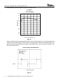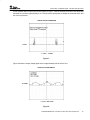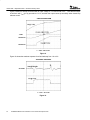
1
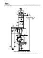
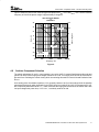
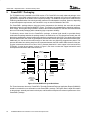
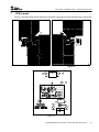
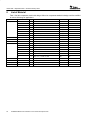
User’s Guide TPS40003 Based 5–A Converter in Less Than One Square Inch User’s Guide EVM IMPORTANT NOTICE Texas Instruments (TI) provides the enclosed product(s) under the following conditions: This evaluation kit being sold by TI is intended for use for ENGINEERING DEVELOPMENT OR EVALUATION PURPOSES ONLY and is not considered by TI to be fit for commercial use. As such, the goods being provided may not be complete in terms of required design-, marketing-, and/or manufacturing-related protective considerations, including product safety measures typically found in the end product incorporating the goods. As a prototype, this product does not fall within the scope of the European Union directive on electromagnetic compatibility and therefore may not meet the technical requirements of the directive. Should this evaluation kit not meet the specifications indicated in the EVM User’s Guide, the kit may be returned within 30 days from the date of delivery for a full refund. THE FOREGOING WARRANTY IS THE EXCLUSIVE WARRANTY MADE BY SELLER TO BUYER AND IS IN LIEU OF ALL OTHER WARRANTIES, EXPRESSED, IMPLIED, OR STATUTORY, INCLUDING ANY WARRANTY OF MERCHANTABILITY OR FITNESS FOR ANY PARTICULAR PURPOSE. The user assumes all responsibility and liability for proper and safe handling of the goods. Further, the user indemnifies TI from all claims arising from the handling or use of the goods. Please be aware that the products received may not be regulatory compliant or agency certified (FCC, UL, CE, etc.). Due to the open construction of the product, it is the user’s responsibility to take any and all appropriate precautions with regard to electrostatic discharge. EXCEPT TO THE EXTENT OF THE INDEMNITY SET FORTH ABOVE, NEITHER PARTY SHALL BE LIABLE TO THE OTHER FOR ANY INDIRECT, SPECIAL, INCIDENTAL, OR CONSEQUENTIAL DAMAGES. TI currently deals with a variety of customers for products, and therefore our arrangement with the user is not exclusive. TI assumes no liability for applications assistance, customer product design, software performance, or infringement of patents or services described herein. Please read the EVM User’s Guide and, specifically, the EVM Warnings and Restrictions notice in the EVM User’s Guide prior to handling the product. This notice contains important safety information about temperatures and voltages. For further safety concerns, please contact the TI application engineer. Persons handling the product must have electronics training and observe good laboratory practice standards. No license is granted under any patent right or other intellectual property right of TI covering or relating to any machine, process, or combination in which such TI products or services might be or are used. Mailing Address: Texas Instruments Post Office Box 655303 Dallas, Texas 75265 Copyright 2003, Texas Instruments Incorporated 2 DYNAMIC WARNINGS AND RESTRICTIONS It is important to operate this EVM within the input voltage range of 0 V to 5.5 V. Exceeding the specified input range may cause unexpected operation and/or irreversible damage to the EVM. If there are questions concerning the input range, please contact a TI field representative prior to connecting the input power. Applying loads outside of the specified output range may result in unintended operation and/or possible permanent damage to the EVM. Please consult the EVM User’s Guide prior to connecting any load to the EVM output. If there is uncertainty as to the load specification, please contact a TI field representative. During normal operation, some circuit components may have case temperatures greater than 50°C. The EVM is designed to operate properly with certain components above 50°C as long as the input and output ranges are maintained. These components include but are not limited to linear regulators, switching transistors, pass transistors, and current sense resistors. These types of devices can be identified using the EVM schematic located in the EVM User’s Guide. When placing measurement probes near these devices during operation, please be aware that these devices may be very warm to the touch. Mailing Address: Texas Instruments Post Office Box 655303 Dallas, Texas 75265 Copyright 2003, Texas Instruments Incorporated 3 SLUU130A – September 2002 – Revised February 2003 TPS40003-Based 5-A Converter in Less Than One Square Inch Mark Dennis Systems Power Contents 1 Introduction . . . . . . . . . . . . . . . . . . . . . . . . . . . . . . . . . . . . . . . . . . . . . . . . . . . . . . . . . . . . . . . . . . . . . . . . . 4 2 Features . . . . . . . . . . . . . . . . . . . . . . . . . . . . . . . . . . . . . . . . . . . . . . . . . . . . . . . . . . . . . . . . . . . . . . . . . . . . 4 3 Schematic . . . . . . . . . . . . . . . . . . . . . . . . . . . . . . . . . . . . . . . . . . . . . . . . . . . . . . . . . . . . . . . . . . . . . . . . . . . 5 4 Design Procedure . . . . . . . . . . . . . . . . . . . . . . . . . . . . . . . . . . . . . . . . . . . . . . . . . . . . . . . . . . . . . . . . . . . . 6 5 PowerPAD Packaging . . . . . . . . . . . . . . . . . . . . . . . . . . . . . . . . . . . . . . . . . . . . . . . . . . . . . . . . . . . . . 10 6 Test Results/Performance Data . . . . . . . . . . . . . . . . . . . . . . . . . . . . . . . . . . . . . . . . . . . . . . . . . . . . . . 11 7 PCB Layout . . . . . . . . . . . . . . . . . . . . . . . . . . . . . . . . . . . . . . . . . . . . . . . . . . . . . . . . . . . . . . . . . . . . . . . . 15 8 List of Material . . . . . . . . . . . . . . . . . . . . . . . . . . . . . . . . . . . . . . . . . . . . . . . . . . . . . . . . . . . . . . . . . . . . . 16 1 Introduction The TPS40002 and the TPS40003 are voltage-mode, synchronous buck PWM controllers that utilize TI’s proprietary Predictive Gate Drive technology to wring maximum efficiency from step-down converters. These controllers provide a bootstrap charging circuit to allow the use of an N-channel MOSFET as the topside buck switch to reduce conduction losses and increase silicon device utilization. Predictive Gate Drive technology controls the delay from main switch turn-off to synchronous rectifier turn-on and also the delay from rectifier turn-off to main switch turn-on. This allows minimization of the losses in the MOSFET body diodes by reducing conduction and reverse recovery time. This user’s guide provides details on a 5-A buck converter that converts 3.3 V down to a 1.2-V level utilizing the TPS40003 controller, with less than one square inch board area. A schematic for the board is shown in Figure 1. A list of material is provided in the final section. 2 Features The specification for this board is as follows: D D D D D D 4 VIN = 3.0 V to 3.6 V VOUT = 1.2 V ± 3% 0 A ≤ IOUT ≤ 5 A Efficiency > 90% with a load of 2 A Output voltage ripple < 2% VOUT Physical size < 1 square inch circuit area TPS40003-Based 5-A Converter in Less Than One Square Inch SLUU130A – September 2002 – Revised February 2003 Schematic + 3 Figure 1. Application Diagram for the TPS40002/3 TPS40003-Based 5-A Converter in Less Than One Square Inch 5 SLUU130A – September 2002 – Revised February 2003 4 Design Procedure 4.1 TPS4000X Family Device Selection The TPS4000X family of devices offers four selections to encompass the frequency and output current mode choices. The TPS40003 is selected for the following reasons. First, the internal oscillator components set a fixed switching frequency of 600 kHz. This allows minimally sized filter components in this compact design. The other choice related to the TPS4000X family involves the selection of Discontinuous Current Mode (DCM) operation or Continuous Current Mode (CCM) operation at lighter loads. In this design the TPS40003 is selected to keep the current continuous all the way to zero load, to provide robust control characteristics. 4.2 Inductance Value The output inductor value is selected to set the ripple current to a value most suited to overall circuit functionality. The inductor value is calculated in equation (1). L+ ȡ1 * VOUT ȣ+ 1.2 V VǓ + 1.07 mH ǒ1 * 1.2 ȧ 600 kHz 1.25 A 3.6 V V I RIPPLEȧ Ȣ IN(max)Ȥ V OUT f (1) where IRIPPLE is chosen to be 25% of IOUT, or 1.25 A. A common value of 1 µH is selected. 4.3 Input Capacitor Selection Bulk input capacitor selection is based on allowable input voltage ripple and required RMS current carrying capability. In typical buck converter applications, the converter is fed from an upstream power converter with its own output capacitance. In this converter, onboard capacitance is provided to supply the current required during the top MOSFET on-time while keeping ripple within acceptable limits. For this power level, input voltage ripple of 150 mV is reasonable, and a conservative minimum value of capacitance is calculated in equation (2). C+I Dt + 5 A 606 ns + 20 mF 0.15 V DV (2) To meet this requirement with the lowest size and cost, a single 22 µF, X5R ceramic capacitor might be considered. Although these capacitors have an extremely small resistance a typical datasheet indicates that the part undergoes a 30°C temperature rise with 2 ARMS current at 500 kHz. With VIN = 3.0 V our circuit requires nearly 2 ARMS of current, so for a conservative design two capacitors are selected to allow for conservative current derating. These capacitors function as power bypass components and should be located near the MOSFET package, to keep the high frequency current flow in a tight loop. The low impedance characteristics of the dual ceramic capacitors help to reduce noise on the VDD supply of the device. Specifically, the high side MOSFET current sense is referenced to this point, so noise at the device must be kept to a low level. 6 TPS40003-Based 5-A Converter in Less Than One Square Inch SLUU130A – September 2002 – Revised February 2003 4.4 Output Capacitor Selection Selection of the output capacitor is based on many application variables, including function, cost, size, and availability. The minimum allowable output capacitance is determined by the amount of inductor ripple current and the allowable output ripple in equation (3). C OUT(min) + I RIPPLE 8 f V RIPPLE + 1.25 A + 22 mF 600 kHz 12 mV 8 (3) In this design, COUT(min) is 22 µF with VRIPPLE = 12 mV to allow for some margin. However, this only affects the capacitive component of the ripple voltage. In addition, the voltage component due to the capacitor ESR must be considered in equation (4). V ESR Cout v RIPPLE + 0.012 V + 9.6 mW 1.25 A I RIPPLE (4) For compactness while maintaining transient response capability, two 22-µF ceramic capacitors are fitted in parallel. The total ESR of these capacitors is below 3 mΩ, and contributes only a few mV to the output voltage ripple. 4.5 MOSFET Selection The small physical size of this design requires the use of a single SO-8 package which contains dual N-channel MOSFETs. MOSFETs with an RDS(on) of 18 mΩ are selected to keep the conduction losses to a manageable amount at full load. 4.6 Short Circuit Protection The TPS40003 implements short circuit protection by comparing the voltage across the topside MOSFET while it is on to a voltage dropped from VDD by RLIM due to an internal current source of 15 µA inside pin 1. Due to tolerances in the current source and variations in the power MOSFET on-voltage versus temperature, the short circuit level can protect against gross overcurrent conditions only, and should be set higher than rated load. In this particular case, RLIM is selected as: R LIM + R1 + 2.5 I OUT 15 mA 0.018 W + 15 kW (5) For this design, RLIM = 15 kΩ, and the factor of 2.5 in the equation accounts for the variations in component tolerances over temperature and output current ripple. The high currents that are switched under short circuit conditions may cause SW pin 8 to be driven below ground several volts, possibly injecting substrate current which can cause improper operation of the device. A 3.3-Ω resistor has been placed in series with this pin to limit its excursion to safe levels. TPS40003-Based 5-A Converter in Less Than One Square Inch 7 SLUU130A – September 2002 – Revised February 2003 4.7 Compensation Design The TPS40003 uses voltage mode control in conjunction with a high frequency error amplifier. For the fastest transient response, the loop crossover frequency is set at 1/10 fS, or 60 kHz. The power circuit L-C double pole corner frequency fC is situated at 24 kHz, and the output capacitor ESR zero is far higher at approximately 1MHz. The feedback compensation network is implemented to provide two zeroes and three poles. The first pole is placed at the origin to improve dc regulation. The first zero is placed at approximately 2/3 fC, 18 kHz, f z1 + 2 p 1 R2 (6) C4 The second zero is selected at fC, f z2 + 2 p 1 ǒR4 ) R5Ǔ C 12 (7) The two poles are placed at approximately 300 kHz, which is one-half the switching frequency, 1 f p1 + 2 p R2 ǒ 1 R5 C 12 C C 4 C )C 4 Ǔ 8 (8) 8 and f p2 + 8 2 p TPS40003-Based 5-A Converter in Less Than One Square Inch (9) SLUU130A – September 2002 – Revised February 2003 Figure 2 shows the plots for the closed loop gain and phase with VIN = 3.3 V and IOUT = 4.4 A. At the crossover frequency of 60 kHz the phase margin is approximately 51 degrees. GAIN AND PHASE MARGIN vs FREQUENCY 150 40 30 Phase 100 Gain – db 50 10 0 0 –10 Phase – degrees 20 –50 Gain –20 –30 –100 ILOAD = 4.4 A VI = 3.3 V –150 –40 100 1000 10000 100000 1000000 Frequency – Hz Figure 2. 4.8 Snubber Component Selection The switch node where Q1 and L1 come together is very noisy. An R–C network fitted between this node and ground can help reduce ringing and voltage overshoot on Q1:B. This ringing noise should be minimized to prevent it from confusing the control circuitry which is monitoring this node for current limit and Predictive Gate Drive. As a starting point, the snubber capacitor, C9, is generally chosen to be 5 to 8 times larger than the parasitic capacitance at the node, which is primarily COS of Q1:B. Since COS is 440 pF for Q1:B, C9 is chosen to be 3.3 nF. R3 is empirically determined to be 2.2 Ω, which minimizes the ringing and overshoot at the switch node. With low input voltages the power loss, 1/2×C×V2×f , is relatively small at 24 mW. TPS40003-Based 5-A Converter in Less Than One Square Inch 9 SLUU130A – September 2002 – Revised February 2003 5 PowerPAD Packaging The TPS4000X family is available in the DGQ version of TI’s PowerPAD thermally enhanced package. In the PowerPAD, a thermally conductive epoxy is utilized to attach the integrated circuit die to the leadframe die pad, which is exposed on the bottom of the completed package. The leadframe die pad can be soldered to the PCB using standard solder flow techniques when maximum heat dissipation is required. However, depending on power dissipation requirements, the PowerPAD may not need to soldered to the PCB. The PowerPAD package helps to keep the junction temperature rise relatively low even with the power dissipation inherent in the onboard MOSFET drivers. This power loss is proportional to switching frequency, drive voltage, and the gate charge needed to enhance the N-channel MOSFETs. Effective heat removal allows the use of ultra small packaging while maintaining high component reliability. To effectively remove heat from the PowerPAD package, a thermal land should be provided directly underneath the package whether the package needs to be soldered or not. This thermal land usually has vias that help to spread heat to internal copper layers and/or the opposite side of the PCB. The vias should not have thermal reliefs that are often used on ground planes, because this reduces the copper area which transfers heat. Additionally, the vias should be small enough so that the holes are effectively plugged when plated. This prevents the solder from wicking away from the connection between the PCB surface and the bottom of the part. A typical construction utilizes a few vias of 0.013” diameter plated with 1 ounce copper in the land under the TPS40003. A typical layout pattern is shown in Figure 2, but does not show the copper land which would encompass the vias above and below the device. 2.92mm (0.115”) 0.5mm (0.0197”) Minimum PowerPad ”Y” 1.7mm (0.068”) 0.28mm (0.011”) 1.40mm (0.055”) Via Dia. 0.33mm (0.013”) Miminum PowerPad ”X” 1.3mm (0.050”) Figure 3. PowerPAD PCB Layout Guidelines The Texas Instrument document, PowerPAD Thermally Enhanced Package Application Report (SLMA002) should be consulted for more information on the PowerPAD package. This report offers in-depth information on the package, assembly and rework techniques, and illustrative examples of the thermal performance of the PowerPAD package. 10 TPS40003-Based 5-A Converter in Less Than One Square Inch SLUU130A – September 2002 – Revised February 2003 6 Test Results/Performance Data The test setup is shown in figure 4 DC Power Supply Input wires 18 gauge or larger short as feasible C IN DVM1 + CIN = 470 µF or larger, 6.3 V or higher, low ESR AIEA or OSCON capacitor. Place within 2 inches of J1. (–) (+) J1 TP2 TP1 GND VIN TP3 SCOPE TP5 SLUP182 GND TP6 VOUT J2 DVM2 TP4 (+) (–) Output wires 18 gauge or larger short as feasible Resistive load: 0.5 Ω, ≥ 5 W Active Load: set for 2.4 A (–) LOAD (+) Figure 4. TPS40003-Based 5-A Converter in Less Than One Square Inch 11 SLUU130A – September 2002 – Revised February 2003 Typical efficiency curves are shown in Figure 5 for an input of 3.3 V. EFFICIENCY vs OUTPUT CURRENT 100 95 Efficiency – % 90 85 80 75 70 65 60 55 50 0 1 2 3 4 5 6 IOUT – Output Current – A Figure 5. Figure 6 shows the switch node during typical operation at full load. Note that there is very minimal body diode conduction in the bottom MOSFET. This is a result of using the predictive delay control implementation. This technique is able to dynamically change the delays in the MOSFET drive circuit to account for variations in line, load, and between devices. TYPICAL SWITCH NODE WAVEFORM 2 V/div t – Time – 250 ns/div Figure 6. 12 TPS40003-Based 5-A Converter in Less Than One Square Inch SLUU130A – September 2002 – Revised February 2003 Circuit operation with an output short circuit is shown in Figure 7. After each restart into a short circuit the pulses terminate for a period of approximately 6 ms. This causes the input power to collapse to minuscule levels, and the circuit is protected. SHORT CIRCUIT OPERATION 2 V/div t – Time – 1 ms/div Figure 7. Figure 8 shows the output voltage ripple which is approximately half the 24-mV limit. OUTPUT VOLTAGE RIPPLE 10 mV/div t – Time – 500 ns/div Figure 8. TPS40003-Based 5-A Converter in Less Than One Square Inch 13 SLUU130A – September 2002 – Revised February 2003 Figure 9 shows the startup waveforms with an input voltage of 3.3 V and a load of 0.3 Ω. Note that the output is held low until VSS (pin 4) goes above 0.12 V, and then the output comes up smoothly under closed loop softstart control. STARTUP WAVEFORM 1 V/div 500 mV/div 500 mV/div t – Time – 200 µs/div Figure 9. Figure 10 shows the transient response for a fast load step from 1 A to 2 A. TRANSIENT RESPONSE 50 mV/div t – Time – 20 µs/div Figure 10. 14 TPS40003-Based 5-A Converter in Less Than One Square Inch SLUU130A – September 2002 – Revised February 2003 7 PCB Layout Figures 11 through13 show the top copper layer, the bottom copper layer, and top assembly layer, of SLUP182. Figure 12 Figure 13 TPS40003-Based 5-A Converter in Less Than One Square Inch 15 SLUU130A – September 2002 – Revised February 2003 8 List of Material Table 1 lists the components used in this design. With minor component tweaks this design could be modified to meet a wide range of applications. Reference Capacitor Terminal Block 16 Qty Description Manufacturer Part Number C1, C2, C5, C6 4 Ceramic, 22 µF, 6.3 V, X5R, 20%, 1210 Panasonic ECJ–4YB0J226M C10 1 Ceramic, 0.001 µF, 10 V, X5R, 10%, 805 Panasonic ECJ–2YB1A105K C11 1 Ceramic, 0.0047 µF, 50 V, X7R, 10% Vishay VJ0603Y472KXAAT C12 1 Ceramic, 470 pF, 50 V, X7R, 10% Vishay VJ0603Y471KXAAT C3 1 Ceramic, 0.1 µF, 50 V, X5R, 10% Vishay VJ0805Y104KXAAT C4 1 Ceramic, 0.001 µF, 50 V, X7R, 10% Vishay VJ0603Y102KXAAT C8 1 Ceramic, 68 pF, 50 V, NPO, 10% Vishay VJ0603A680KXAAT C9 1 Ceramic, 0.0033 µF, 50 V, X7R, 10% Vishay VJ0805Y332KXAAT J1, J2 2 2 pin, 15 A, 5.1 mm OST ED1609 Inductor L1 1 SMT, 1.0 µH, 8.5 A, 10 mΩ Vishay IHLP–2525CZ–01 MOSFET Q1 1 Dual N–channel, 20 V, 9.4 A, 18 mΩ Fairchild FDS6898A Resistor R1 1 Chip, 15 kΩ, 1/16W, 1% Std Std R2 1 Chip, 8.66 kΩ, 1/16 W, 1% Std Std R3 1 Chip, 2.2 Ω, 1/10 W, 5% Std Std R4 1 Chip, 12.1 kΩ, 1/16 W, 1% Std Std R5 1 Chip, 1 kΩ, 1/16 W, 1% Std Std R6 1 Chip, 16.9 Ω, 1/16 W, 1% Std Std R7 1 Chip, 3.3 Ω, 1/16 W, 5%, 603 Std Std JACK TP1, TP3, TP4, 5 Test point, red Farnell 240–345 JACK TP2, TP6 2 Test point, black Farnell 240–333 Adaptor TP5 1 3.5-mm probe clip (or 131–5031–00) Tektronix 131–4244–00 Device U1 1 Syncronous buck controller, 600 kHz TI TPS40003DGQ TPS40003-Based 5-A Converter in Less Than One Square Inch IMPORTANT NOTICE Texas Instruments Incorporated and its subsidiaries (TI) reserve the right to make corrections, modifications, enhancements, improvements, and other changes to its products and services at any time and to discontinue any product or service without notice. Customers should obtain the latest relevant information before placing orders and should verify that such information is current and complete. All products are sold subject to TI’s terms and conditions of sale supplied at the time of order acknowledgment. TI warrants performance of its hardware products to the specifications applicable at the time of sale in accordance with TI’s standard warranty. Testing and other quality control techniques are used to the extent TI deems necessary to support this warranty. Except where mandated by government requirements, testing of all parameters of each product is not necessarily performed. TI assumes no liability for applications assistance or customer product design. Customers are responsible for their products and applications using TI components. To minimize the risks associated with customer products and applications, customers should provide adequate design and operating safeguards. TI does not warrant or represent that any license, either express or implied, is granted under any TI patent right, copyright, mask work right, or other TI intellectual property right relating to any combination, machine, or process in which TI products or services are used. Information published by TI regarding third–party products or services does not constitute a license from TI to use such products or services or a warranty or endorsement thereof. Use of such information may require a license from a third party under the patents or other intellectual property of the third party, or a license from TI under the patents or other intellectual property of TI. Reproduction of information in TI data books or data sheets is permissible only if reproduction is without alteration and is accompanied by all associated warranties, conditions, limitations, and notices. Reproduction of this information with alteration is an unfair and deceptive business practice. TI is not responsible or liable for such altered documentation. Resale of TI products or services with statements different from or beyond the parameters stated by TI for that product or service voids all express and any implied warranties for the associated TI product or service and is an unfair and deceptive business practice. TI is not responsible or liable for any such statements. Mailing Address: Texas Instruments Post Office Box 655303 Dallas, Texas 75265 Copyright 2003, Texas Instruments Incorporated