1
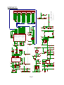
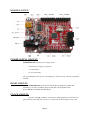
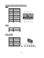
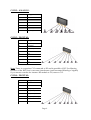
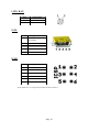
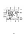
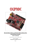
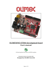
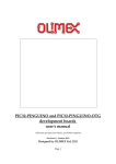
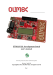
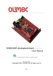
OLIMEXINO-328 development board
Users Manual
All boards produced by Olimex are ROHS compliant
Revision A, August 2011
Designed by OLIMEX Ltd, 2011
Page 1
INTRODUCTION:
What is Arduino?
Arduino is an open-source electronics prototyping platform, designed to make the
process of using electronics in multidisciplinary projects more accessible. The hardware consists of a simple open hardware design for the Arduino board with an Atmel AVR processor and on-board I/O support. The software consists of a standard
programming language and the boot loader that runs on the board.
Arduino hardware is programmed using a Wiring-based language (syntax + libraries), similar to C++ with some simplifications and modifications, and a Processing-based IDE.
The project began in Ivrea, Italy in 2005 to make a device for controlling student-built interaction design projects less expensively than other prototyping systems available at the time. As of February 2010 more than 120,000 Arduino boards
had been shipped. Founders Massimo Banzi and David Cuartielles named the project after a local bar named Arduino. The name is an Italian masculine first name,
meaning "strong friend". The English pronunciation is "Hardwin", a namesake of
Arduino of Ivrea
More information could be found at the creators web page http://arduino.cc/ and
in the Arduino Wiki http://en.wikipedia.org/wiki/Arduino
To make the story short - Arduino is easy for the beginners with lack of Electronics
knowledge, but also do not restrict the professionals as they can program it in C++
or mix of Arduino/C++ language.
There are thousands of projects which makes the startup easy as there is barely no
field where Arduino enthusiasts to have not been already.
Page 2
BOARD FEATURES:
We enter in Arduino field 5 years after the design was introduced, and this allowed
us to see and skip all the errors the Arduino inventors did :-)
We had the possibility to read current customer feedback and to implement what
they wanted to see in the original Arduino.
There are few thinks which we made better than the original Arduino design:
1.
We allow the board to work at different frequencies with easily exchange of
the quartz crystal.
2.
Original Arduino uses linear power supply, this limits the input voltage
range. We designed the power supply to accept power from 9 to 30V DC thus making possible to take virtually any power supply adapter on the market, also enable
application which are in industrial power supply 24VDC.
3.
We carefully selected all components to work reliable in INDUSTIRAL
temperature range -25+85C so the board can be used in INDUSTIRAL applications
while the original design is to Commercial 0-70C operating temperature.
4.
The original Arduino design is not good for portable applications as consumes too much power with the linear vltage regulators, we put ULTRA LOW
POWER voltage regulators and the consumption is only few microamps, which enables handheld and battery powered applications.
5.
We add Li-Ion rechargable battery power supply option with BUILD-IN on
board charger, so when you attach battery it is automatically charged and kept in
this state until the other power source (USB or external adapter) is removed and it
AUTOMATICALLY will power the board - no jumpers, no switches!
6.
switch.
Our design can work both on 3.3V and on 5V which is selectable with
7.
Our board have UEXT connector which allow many existing modules like
RF, ZIGBEE, GSM, GPS to be connected.
8.
Our desing allow RTC - Real Time Clock.
9.
We made our design noise immune, there are number of threads on Arduino forum for problems with the RESET when board works with motors, this is because Atmel recommendations were omited in the original design, we fixed this.
10.
We use separate voltage regulator for the Analog part, which allow the
ADC to be read correctly without the digital noise pickup.
11.
Optionally if someone need higher precision and temperature stability in
Analog reading we have provision on the board for Aref preciese source.
12.
The LEDs and the BUTTONs are on the edge of the board so there is easy
access even if the boards have shields on them.
13.
All components are LOWER than the connectors, so the shields do not interference with them.
Page 3
14.
mini USB connector is used which is common and used in most cell phones,
so you do not have to buy other cables
15.
Original design had flaw and the connectors were not spaced at 0.1" this
make perfo board use impossible, to keep the compatibility we have same spacing
but we add next to this connector on 0.1" which customer can use with perforated
boards.
16.
All signals on the connectors are printed on top and on bottom of the board,
so when you check with probe you know exactly which port you are measuring.
17.
4 mount holes make board attachment easier
ELECTROSTATIC WARNING:
The OLIMEXINO-328 board is shipped in protective anti-static packaging. The
board must not be subject to high electrostatic potentials. General practice for
working with static sensitive devices should be applied when working with this
board.
BOARD USE REQUIREMENTS:
Cables:
You will need mini USB cable for connecting the board to PC. For
programming – the cable you will need depends on the programmer/debugger
you use. If you use AVR-ISP500, AVR-ISP500-TINY or AVR-ISP500-ISO, you will
need USB A-B cable.
Programmer/Debugger AVR-ISP500, AVR-ISP500-TINY,
AVR-ISP500-ISO or other compatible programming/debugging tool.
Hardware:
Page 4
USB
GND1
GND2
VBUS
DD+
ID
GND
USB
GND3
GND4
Page 5
C23
8
7
DC
IS
6
VCC
1N5819S
SD2
VSS
R7
330R
+5V
IS-1390(Default: 5V is closed)
3
GYX-SD-TC0805SURK(RED)
PWR
3
R4
1k/1%
R3
3k/1%
2
6
R26
10k
2
4
6
8
10
BH10R
UEXT
R25
10k
0R(NA)
0R
R27
L2
22uH/10%/5mA
DVCC
D0(RXD)
A4(SDA)
D11(MOSI)
UEXT_CS
R24
4.7k
AVCC
D7 1
3
D7
R12
4.7k
DVCC
D10(#SS)
RST
D7:Close;D10:Open
D7/D10
D7
D6
D5
D4
D3
D2(BUT)
D1(TXD)
D0(RXD)
11
10
9
2
1
32
31
30
DVCC
RESET
A5(SCL)
A4(SDA)
A3
A2
A1
A0
29
28
27
26
25
24
23
DVCC
PCINT23/AIN1/PD7
PCINT22/OC0A/AIN0/PD6
PCINT21/OC0B/T1/PD5
PCINT20/XCK/T0/PD4
PCINT19/OC2B/INT1/PD3
INT0/PCINT18/PD2
TXD/PCINT17/PD1
RXD/PCINT16/PD0
PC6/#RESET/PCINT14
PC5/ADC5/SCL/PCINT13
PC4/ADC4/SDA/PCINT12
PC3/ADC3/PCINT11
PC2/ADC2/PCINT10
PC1/ADC1/PCINT9
PC0/ADC0/PCINT8
XTAL2
XTAL1
D13(SCK/LED1)
D12(MISO)
D11(MOSI)
D10(#SS)
D9(LED2)
D8
8
7
17
16
15
14
13
12
4.7nF
C7
RESET
1N4148/mini-melf
SD5
C8
BUT
1
2
3
4
5
6
R21
4.7k
2
DTR
D2(BUT)
ISP1
ISP2
ISP3
ISP4
ISP5
ISP6
D8
D9
D10
D11
D12
D13
GND
AREF
D0
D1
D2
D3
D4
D5
D6
D7
A0
A1
A2
A3
A4
A5
RST
3V3
5V
GND
GND
VIN
SIDE_WT CM -T R(3X4)
2
330R
R13
C6 10nF
C5 10uF/6.3V
C4 10uF/6.3V
C3 100nF
10uF/6.3V
G
10uF/6.3V
+
CE 470uF/10V/6.3x11mm/RM2.5
4
C2 100nF
C20 820pF
+
CE 100uF/35V/6.3x11m m/RM2.5
http://www.olimex.com/dev
DESIGNED BY OLIMEX LTD, 2011
Rev. B
OLIMEXINO-328
Close
100nF
C12
NA(PN1X8)
1
2
3
4
5
6
7
8
NA(PN1X8)
CON4
1
2
3
4
5
6
7
8
NA(PN1X6)
CON3
USB_RST
1
1
2
3
4
5
6
CO N1
NA(PN1X6)
CON2
DVCC
D13(SCK/LED1)
D11(MOSI)
RESET
GND
D12(MISO)
D8
D9(LED2)
D10(#SS)
D11(MOSI)
D12(MISO)
D13(SCK/LED1)
GND
AREF
D0(RXD)
D1(TXD)
D2(BUT)
D3
D4
D5
D6
D7
100nF
DVCC
RESET
A0
A1
A2
A3
A4(SDA)
A5(SCL)
VIN
3.3V
+5V
330R
R22
U3
MC33063ADR(SO8)
D
C22
SW(3.3V/5V)
1
2
C21
SD3
1N5819S
3.3V
1
5
5
L3
CL10uH SW68
+5V
Q1
SIDE_WT CM-TR(3X4)
FB
1
2
C24 2.2uF
SC
SE
FET1
IRLML6402
3
4
TC
S
3
5V_USB
GND
VOUT
VIN
3.3V
6
C1
-
1
2
VR1
MCP1700T-3302E/MB
R23
4.7k
G ND
Q16.000MHz/HC-49S/20pF/20ppm/PTH
39pF
39pF
NA Q2
PCINT7/XTAL2/TOSC2/PB7
PCINT6/XTAL1/TOSC1/PB6
SCK/PCINT5/PB5
PCINT4/MISO/PB4
PCINT3/OC2A/MOSI/PB3
PCINT2/#SS/OC1B/PB2
PCINT1/OC1A/PB1
PCINT0/CLKO/ICP1/PB0
C18
C17
ATmega328P-AU
ADC6
ADC7
AGND
AVCC
AREF
GND
GND
DVCC
19
22
21
C16
100nF
18
AVCC
20
5
3
U1
VCC
VCC
1
D1(TXD)
3
A5(SCL)
5
D12(MISO)
7
D13(SCK/LED1) 9
A6
A7
DVCC
C15
100nF
0R(NA)
0R
R6
AREF
100nF
5
X1-2
NA
0.47R
0.47R
R2
R1
DW02R
1
2
LIPO_BAT
NA(HR1X6)
6
5
4
3
2
1
FTDI_BASIC
C14
100nF
4
6
4
YDJ-1136
9-30VDC
PWR_J
SD1
1N5819S
VIN
15k
2.2uF
C27
+
R28
5
1
Green(0603)
RX
Red(0603)
10k
C13
DVCC
5V_USB
330R
TX
LED2
YELLOW(GYX-SD-TC0805SYC)
R15
330R
0R
R5
1k D0(RXD)
1k D1(TXD)
0R(NA)
D9(LED2)
CTS
DVCC
TXO
RXI
DTR
R19
R18
CTS
DTR
TXO R16
RXI R17
C25 2.2uF
X1-1
VSSPROG
D
BATTERY CE
CHARGER
FET2
IRLML6402
S
MCP73812T-420I/OT
2
3
+5V
SD4
1N5819S
2.2uF
VDDVBAT
U4
LED1
GREEN(GYX-SD-TC0805SGC)
G
4
Battery Charger
A
R8
330R
D13(SCK/LED1)
23
22
13
14
12
1
5
3
11
2
9
10
6
DIGITAL
C26
+5V
R
SR1
NA(ZTL431AFTA)
2
CBUS0
CBUS1
CBUS2
CBUS3
CBUS4
TXD
RXD
RTS#
CTS#
DTR#
DSR#
DCD#
RI#
DIGITAL
R11
NA
C
10uF/6.3V
Close
GND
AGND
7
25
FT232RL(SSOP28)
18
1
3V3OUT
NC1
#RESET
NC2
OSCI
OSCO
USBDM
USBDP
VCCIO
VCC
U2
GND
LED1_E
17
8
19
24
27
28
16
15
4
20
ANALOG
R10
NA
C10 100nF
AREF
10k
R30
26
21
R9
NA
4.7k
R20
100nF
C11
DVCC
FT232RL
TEST
GND
R14
NA
AVCC
C9
C19
10nF
USB-MINI
5V_USB
POWER
VIN
L1
FB /6 00 O HM /1 20 6 (3 2 16 1 1 C -6 0 1)
SCHEMATIC:
ARDUINO: PLATFORM & CONNECTORS
ICSP
BOARD LAYOUT:
POWER SUPPLY CIRCUIT:
OLIMEXINO-328 can take power supply from:
–
external power supply (9-30) VDC.
–
+ 5V from USB
–
3.7 V Li-ion battery
The programmed board power consumption is about 20 mA with all peripherals
enabled
RESET CIRCUIT:
OLIMEXINO-328 reset circuit includes R12 (4.7kΩ), R13 (330Ω), SD5
(1N4148), C7 (4.7nF), C8(100nF), jumper USB_RST, ATmega328P pin29
(PC6/3RESET/PCINT14) and RST button.
CLOCK CIRCUIT:
Quartz crystal Q1 16 MHz is connected to ATmega328P pin 7 (XTAL1) and
pin 8 (XTAL2). Note that the crystal is on socket and can be changed to any value.
Page 6
JUMPER DESCRIPTION:
USB_RST
LED1_E
D7/D10
This jumper, when closed, enables USB autoreset function. After reset the
bootloader is started and loads the program into the Flash.
Default state is closed.
This jumper, when closed, connects LED1 to D13(SCK) line.
Default state is closed.
When this jumper is closed in position D7 – UEXT pin 10 (UEXT_CS) is connected to
Atmega328P pin 11 (PD7) – signal D7, when this jumper is closed in position D10 - –
UEXT pin 10 (UEXT_CS) is connected to Atmega328P pin 14 (PB2/#SS) – signal
D10(3SS).
Default state is closed in position D7.
INPUT/OUTPUT:
Status Led with name LED1 (green) connected via jumper LED1_E to ATmega328P
pin 17 (SCK/PCINT5/PB5) – signal D13(SCK/LED1).
Status Led with name LED2 (yellow) connected to ATmega328P pin 13
(PCINT1/OC1A/PB1) – signal D9(LED2).
Status Led with name TX (red) indicates that there is transfer in the FTDI.
Status Led with name RX (green) indicates that there is transfer in the FTDI.
Power-on LED (red) with name PWR – this LED shows that the board is power
supplied.
User button with name BUT connected to ATmega328P pin 32
(INT0/PCINT18/PD2) – signal D2(BUT).
User button with name RST connected to ATmega328P pin 29 (PC6/#RESET).
Switch with name SW(3.3V/5V) – selects between 3.3V and 5V power supply of the
board.
Page 7
EXTERNAL CONNECTORS DESCRIPTION:
UEXT:
Pin #
Signal Name
1
VCC
2
GND
3
D1(TXD)
4
D0(RXD)
5
A5(SCL)
6
A4(SDA)
7
D12(MISO)
8
D11(MOSI)
9
D13(SCK/LED1)
10
UEXT_#CS
PWR_J:
Pin #
Signal Name
1
Power Input
2
GND
CON1 – POWER:
Pin #
Signal Name
1
RESET
2
+3.3V
3
+5V
4
GND
5
GND
6
VIN
Page 8
CON2 – ANALOG:
Pin #
Signal Name
1
A0
2
A1
3
A2
4
A3
5
A4(SDA)
6
A5(SCL)
CON3 – DIGITAL:
Pin #
Signal Name
1
D0(RXD)
2
D1(TXD)
3
D2(BUT)
4
D3
5
D4
6
D5
7
D6
8
D7
Note: There is a capacitor C12 connected to D2 and in parallel to BUT (for filtering
bounces of the BUT) but it can cause interference (and unwanted filtering of signals)
if you want to connect for instance RF module to D2, remove C12.
CON4 – DIGITAL:
Pin #
Signal Name
1
D8
2
D9
3
D10(#SS)
4
D11(MOSI)
5
D12(MISO)
6
D13(SCK/LED1)
7
GND
8
AREF
Page 9
LIPO_BAT:
Pin #
Signal Name
1
VBAT
2
GND
USB:
Pin #
Signal Name
1
+5V_VBUS
(VCCINT)
2
USBDM
3
USBDP
4
Not connected
5
GND
ICSP:
Pin #
Signal Name
1
D12(MISO)
2
VCC
3
D13(SCK/LED1)
4
D11(MOSI)
5
RESET
6
GND
Note, that there is no component mounted for this connector.
Page 10
MECHANICAL DIMENSIONS:
Page 11
AVAILABLE DEMO SOFTWARE:
The software consists of boot loader that runs on the board and a simple blinking
led project.
Page 12
ORDER CODE:
OLIMEXINO-328 - assembled and tested board
How to order?
You can order to us directly or by any of our distributors.
Check our web www.olimex.com/dev for more info.
Revision history:
Board's revision
- Rev. B, March 2011
Manual's revision
- Rev. A, August 2011
- At first page “Copyright(c) 2011, OLIMEX Ltd, All rights
reserved” is replaces with “Designed by OLIMEX Ltd.,
2011”
- In schematic “COPYRIGHT(C) 2011, OLIMEX Ltd.”
replaced with “DESIGNED BY OLIMEX LTD, 2011”
-Rev .B January 2012 – Page 9 – CON3 Important note for
compatibility of RF modules connected to D2 port
Page 13
Disclaimer:
© 2011 Olimex Ltd. Olimex®, logo and combinations thereof, are registered trademarks of Olimex Ltd.
Other terms and product names may be trademarks of others.
The information in this document is provided in connection with Olimex products. No license, express
or implied or otherwise, to any intellectual property right is granted by this document or in
connection with the sale of Olimex products.
Neither the whole nor any part of the information contained in or the product described in this
document may be adapted or reproduced in any material from except with the prior written
permission of the copyright holder.
The product described in this document is subject to continuous development and improvements. All
particulars of the product and its use contained in this document are given by OLIMEX in good faith.
However all warranties implied or expressed including but not limited to implied warranties of
merchantability or fitness for purpose are excluded.
This document is intended only to assist the reader in the use of the product. OLIMEX Ltd. shall not
be liable for any loss or damage arising from the use of any information in this document or any error
or omission in such information or any incorrect use of the product.
Page 14