1
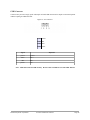
Hercules II EBX
EBX SBC with 800MHz VIA Eden CPU, Integrated Autocalibrating Data Acquisition, and DC/DC Power Supply
User Manual V1.04
© Copyright 2010
1255 Terra Bella Ave.
Mountain View, CA 94043
Tel (650) 810-2500
Fax (650) 810-2525
www.diamondsystems.com
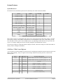
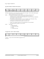
Table of Contents
Introduction......................................................................................................................8
Description and Features...........................................................................................8
Block Diagram..........................................................................................................10
Functional Overview................................................................................................11
Board Description ....................................................................................................14
Connector Summary................................................................................................15
Jumper Summary.....................................................................................................16
Connectors.....................................................................................................................17
PC/104 ISA Bus.......................................................................................................17
PC/104-Plus PCI Bus...............................................................................................18
Utility Connector.......................................................................................................20
Data Acquisition (Digital I/O) Connector..................................................................22
Data Acquisition (Analog I/O) Connector.................................................................24
Ethernet Connectors................................................................................................25
Audio I/O Connector................................................................................................26
Speaker Connector..................................................................................................27
CD Input Connector.................................................................................................28
External Auxiliary Power Connector (Output)..........................................................28
Primary IDE Connector............................................................................................29
Secondary IDE Connector.......................................................................................30
Serial Port I/O Connector.........................................................................................31
External Battery Connector......................................................................................34
USB 1.1 Connectors................................................................................................35
USB1 Connector......................................................................................................36
LCD Panel (LVDS Interface) Connector..................................................................37
VGA Connector........................................................................................................38
Video/TV Out Connector..........................................................................................39
CPU Fan Connector.................................................................................................40
LCD Backlight Connector.........................................................................................40
Low-Voltage Power Input Connector.......................................................................41
High-Voltage Power Input Connector (Optional).....................................................43
CompactFlash Slot (optional)...................................................................................43
Board Configuration......................................................................................................45
Jumper Block J4.......................................................................................................45
Jumper Block J5.......................................................................................................50
Jumper Block J19 - PCI VIO Voltage Selection.......................................................53
Jumper 35 - Crisis Recovery....................................................................................54
System Features............................................................................................................55
System Resources...................................................................................................55
Diamond Systems Corporation
Hercules II-EBX User Manual
Page 2
COM Port / FPGA Control Registers.......................................................................55
Console Redirection to a Serial Port........................................................................56
Watchdog Timer.......................................................................................................57
Failsafe Mode and BIOS Recovery.........................................................................57
Flash Memory..........................................................................................................58
Backup Battery.........................................................................................................58
System Reset...........................................................................................................58
On-Board Video.......................................................................................................58
BIOS................................................................................................................................59
Bios Settings............................................................................................................59
BIOS Download / Crisis Recovery...........................................................................60
BIOS COM Port Settings.........................................................................................61
BIOS Console Redirection Settings.........................................................................62
System I/O......................................................................................................................63
Ethernet....................................................................................................................63
Serial Ports...............................................................................................................63
PS/2 Ports................................................................................................................64
USB Ports................................................................................................................65
Notes on Operating Systems and Booting Procedures............................................66
Windows Operating System Installation Issues.......................................................66
DOS Operating Systems Installation Issues............................................................67
CompactFlash Compatibility Issues Under DOS.....................................................67
Data Acquisition Circuit................................................................................................68
Data Acquisition Circuitry I/O Map...........................................................................69
I/O Register Map Bit Assignments...........................................................................70
I/O Register Definitions............................................................................................73
Data Acquisition Circuit Configuration.......................................................................93
Single-ended/Differential Inputs...............................................................................93
Unipolar/Bipolar Inputs.............................................................................................93
Analog Output Configuration....................................................................................93
Analog-to-Digital Input Ranges and Resolution.........................................................94
Overview..................................................................................................................94
Input Range Selection..............................................................................................94
Input Range Table....................................................................................................94
Performing an A/D Conversion................................................................................95
Select the Input Channel..........................................................................................95
Select the Input Range............................................................................................95
Wait for Analog Input Circuit to Settle......................................................................95
Perform an A/D Conversion on the Current Channel..............................................96
Wait for the Conversion to Finish.............................................................................96
Read the Data from the Board.................................................................................96
Diamond Systems Corporation
Hercules II-EBX User Manual
Page 3
Convert the numerical data to a meaningful value..................................................97
A/D Scan, Interrupt, and FIFO Operation................................................................98
Hercules II A/D Operating Modes............................................................................99
Digital-to-Analog Output Ranges and Resolution....................................................101
Description.............................................................................................................101
Resolution..............................................................................................................101
Output Range Selection.........................................................................................101
D/A Conversion Formulas and Tables...................................................................101
Generating an Analog Output................................................................................103
Analog Circuit Calibration Resources....................................................................105
Analog Circuit Calibration Procedures...................................................................106
Using EEPROM.....................................................................................................107
Reading Value from EEPROM..............................................................................107
Writing Value to EEPROM.....................................................................................107
Digital I/O Operation..............................................................................................108
Special Digital I/O Operation – Port E...................................................................109
DIO Handshaking Operation..................................................................................109
DIO Pull-up/Down Settings....................................................................................110
Counter/Timer Operation............................................................................................112
Counter 0 – A/D Sample Control...........................................................................112
Counter 1 – Counting/Totalizing Functions...........................................................112
Command Sequences...........................................................................................113
Pulse Width Modulation Operation............................................................................116
Pulse-Width Modulation Example..........................................................................117
Watchdog Timer Programming..................................................................................119
Example: Watchdog Timer With Software Trigger...............................................119
Example: Watchdog Timer With Hardware Trigger..............................................119
Data Acquisition Specifications (Data Acquisition units only)...............................120
Analog Inputs.........................................................................................................120
Analog Outputs......................................................................................................120
Digital I/O...............................................................................................................120
Counter/Timers......................................................................................................120
General..................................................................................................................120
FlashDisk Module........................................................................................................121
Installing the FlashDisk Module.............................................................................121
Using the FlashDisk with Another IDE Drive.........................................................121
Power Supply.........................................................................................................122
Utility Board..................................................................................................................123
Diamond Systems Corporation
Hercules II-EBX User Manual
Page 4
FlashDisk Programmer Board....................................................................................124
I/O Cables.....................................................................................................................125
Mounting PC/104(+) Cards onto a Hercules II EBX Baseboard..............................127
CompactFlash..............................................................................................................128
Customization Options...............................................................................................129
Specifications...............................................................................................................130
CPU........................................................................................................................130
Data Acquisition Circuitry.......................................................................................130
Power Supply.........................................................................................................130
General..................................................................................................................130
Additional Information................................................................................................131
Appendix A - Hercules and Hercules II Differences................................................132
Technical Support........................................................................................................133
Figures
Figure 1: Hercules II-EBX Functional Block Diagram......................................................10
Figure 2: Hercules II EBX Board Layout..........................................................................14
Figure 3: J1 and J2 Connectors.......................................................................................17
Figure 4: J3 Connector....................................................................................................18
Figure 5: J6 Connector....................................................................................................20
Figure 6: J7 Connector....................................................................................................20
Figure 7: J8 Connector....................................................................................................22
Figure 8: J9 Connector....................................................................................................24
Figure 9: J10 and J11 Connectors..................................................................................26
Figure 10: J12 Connector................................................................................................26
Figure 11: J13 Connector................................................................................................27
Figure 12: J14 Connector................................................................................................28
Diamond Systems Corporation
Hercules II-EBX User Manual
Page 5
Figure 13: J15 Connector................................................................................................28
Figure 14: J16 Connector................................................................................................29
Figure 15: J17 Connector................................................................................................30
Figure 16: J18 Connector................................................................................................31
Figure 17: J20 Connector................................................................................................34
Figure 18: J21 and J22 Connectors................................................................................35
Figure 19: J23 Connector................................................................................................36
Figure 20: J25 Connector................................................................................................38
Figure 21: J26 Connector................................................................................................39
Figure 22: J27 Connector................................................................................................40
Figure 23: J28 Connector................................................................................................40
Figure 24: J29 Connector................................................................................................41
Figure 25: J30 Connector................................................................................................43
Figure 26: J36 and J37 Connectors................................................................................44
Figure 27: Jumper Block J4 Default Settings..................................................................45
Figure 28: J4 COM3/COM4 IRQ Selection Examples.....................................................47
Figure 29: A/D IRQ Selection Examples.........................................................................48
Figure 30: ATX Power Control Jumper............................................................................48
Figure 31: CMOS RAM Erase Jumper............................................................................49
Figure 32: COM3 and COM4 RS485 Termination Jumpers...........................................49
Figure 33: COM3 and COM4 RS422 Termination Jumpers...........................................50
Figure 34: Jumper Block J5 Default Settings..................................................................50
Figure 35: COM3/COM4 I/O Address Selection..............................................................51
Figure 36: CompactFlash Master/Slave Selection Jumper.............................................52
Figure 37: DIO Pull-up/Pull-down Selection Jumpers.....................................................52
Figure 38: Jumper Block J19...........................................................................................53
Diamond Systems Corporation
Hercules II-EBX User Manual
Page 6
Figure 39: J19 Voltage Selection.....................................................................................54
Figure 40: Watchdog Timer Block Diagram.....................................................................57
Figure 41: Data Acquisition Block Diagram.....................................................................68
Figure 42: DIOLATCH/ACK Handshaking Sequence...................................................110
Figure 43: Flashdisk Module..........................................................................................121
Figure 44: Utility Board..................................................................................................123
Figure 45: FlashDisk Programmer Board Layout..........................................................124
Figure 46: Cable Kit.......................................................................................................126
Figure 47: Differences Between Hercules and Hercules II Boards...............................132
Diamond Systems Corporation
Hercules II-EBX User Manual
Page 7
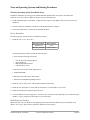
Introduction
Hercules II is an embedded CPU board in an EBX form factor that integrates the following subsystems onto a single
compact board:
•
•
•
•
•
•
CPU
Core PC Chipset (including memory controller, PCI interface, and ISA interface)
Video
Sound
Ethernet
Analog and digital I/O
Hercules II EBX conforms to the EBX standard with expansion support via PC/104-Plus, an embedded standard that
is based on the ISA and PCI buses and provides a compact, rugged mechanical design for embedded systems.
PC/104 modules feature a pin and socket connection system in place of card edge connectors, as well as mounting
holes for stand-offs in each corner. The result is an extremely rugged computer system fit for mobile and miniature
applications. PC/104 modules stack together with 0.6” spacing between boards (0.662” pitch including the
thickness of the PCB).
Hercules II EBX uses the PCI bus internally to connect the Ethernet circuit to the processor. It uses the ISA bus
internally to connect serial ports 3 and 4, as well as the data acquisition circuit, to the processor. Both the ISA and
PCI buses are brought out to expansion connectors for the connection of add-on boards. Diamond Systems
manufactures a wide variety of compatible PC/104 add-on boards for analog I/O, digital I/O, counter/timer
functions, serial ports, and power supplies.
This manual includes:
•
•
•
•
•
•
An introduction to the Hercules II EBX.
Board connectors.
Configuration information.
A description of each of the board subsystems and their usage.
Board specifications.
Additional resource information.
Description and Features
The Hercules II EBX s an upgrade to the existing Hercules product. The board is an all-in-one embedded CPU with
the following key system and data acquisition features.
Processor Section
•
•
•
•
•
•
Pentium-3 class Via Mark Integrated Processor and North Bridge.
265/512MB SDRAM system memory, depending on configuration.
100MHz memory bus.
2MB 16-bit wide integrated flash memory for BIOS and user programs.
2D & 3D VGA Video graphics engine (VESA-style VGA output with DDC Monitor support)
33MHz PCI Bus.
I/O Section
•
•
•
•
•
4 serial ports, 115.2kbaud max.
• 2 ports 16550-compatible
• 2 ports 16850-compatible with 128-byte FIFOs and RS232, RS422 and RS485 capability
4 USB 1.1 ports.
2 IDE drive connectors (standard 40-pin IDE and 44-pin version for notebook drives).
Accepts solid-state flash disk modules directly on board.
Diamond Systems Corporation
Hercules II-EBX User Manual
Page 8
•
•
•
•
•
10/100 BaseT full-duplex PCI bus mastering Ethernet (100Mbps and 10Mbps).
IrDA port (requires external transceiver).
PS/2 keyboard and mouse ports
LEDs.
Interface for speaker and additional external LEDs.
Analog Input
•
•
•
•
•
•
•
32 single-ended / 16 differential inputs, 16-bit resolution
250KHz maximum aggregate A/D sampling rate
Programmable input ranges/gains with maximum range of ±10V / 0-10V
Both bipolar and unipolar input ranges
5 ppm/°C drift accuracy
Internal and external A/D triggering
2048-sample FIFO for reliable high-speed sampling and scan operation
Analog Output
•
•
•
•
4 analog outputs, 12-bit resolution
±10V and 0-10V output ranges
Simultaneous update
Adjustable output range (optional)
Digital I/O
•
•
•
40 programmable digital I/O, 3.3V and 5V logic compatible
Enhanced output current capability: -8/+12mA max
Selectable pull-up/down resistors on board
Counter/Timers
•
•
•
•
•
1 24-bit counter/timer for A/D sampling rate control
1 16-bit counter/timer for user counting and timing functions
Programmable gate and count enable
Internal and external clocking capability
4 programmable pulse width modulation signals with 0 to 100% duty cycle capability
System Features
•
•
•
•
•
•
•
•
•
Plug and play BIOS with IDE auto detection, 32-bit IDE access, and LBA support.
One CompactFlash socket.
Built-in fail-safe boot ROM for system recovery in case of BIOS corruption.
User-selectable COM1 or COM2 terminal mode.
On-board lithium backup battery for real-time-clock and CMOS RAM.
ATX power switching capability.
Programmable watchdog timer
Wide input (5VDC – 28VDC) power supply – Jumper select for 5VDC operation from the PC-104 bus.
Extended temperature range operation (-40 to +85°C).
Diamond Systems Corporation
Hercules II-EBX User Manual
Page 9
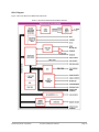
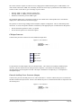
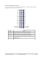
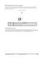
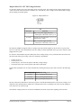
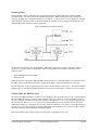
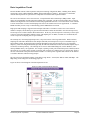
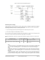
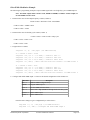
Block Diagram
Figure 1 shows the Hercules II EBX functional blocks.
Figure 1: Hercules II-EBX Functional Block Diagram
Diamond Systems Corporation
Hercules II-EBX User Manual
Page 10
Functional Overview
This section describes the major Hercules II EBX subsystems.
Processor and North Bridge
Hercules II EBX uses the Via Mark CorefusionTM Processor, operating at a frequency of 800MHz. The North
Bridge is integrated in the Via Mark, providing single chip CPU, memory controller and video/LCD/graphics
features .
Hercules II EBX operates with a passive heatsink at the 85°C maximum operating temperature.
South Bridge
The South Bridge chip is the Via VT82C686B. This chip provides standard peripherals of,
•
•
•
•
two serial ports
four USB 1.1 ports
PS/2 keyboard
mouse
The South Bridge chip also generates the ISA bus for use on and off the board.
Memory
The board accommodates either 265MB, or 512MB, of SDRAM system memory, depending on configuration,
soldered on the board. No expansion connector is provided for additional memory.
The board also includes flash memory for storage of BIOS and user programs. Flash memory is accessible via the
on-board ISA bus.
Video Features
The video circuit consists of a Savage 4 2D/3D video accelerator with internal 128-bit 2D and 3D architecture
integrated into the North Bridge chip. It shares up to a 32MB buffer (Unified Memory Architecture) with system
memory, so dedicated video memory chips are not required. Video features include both CRT and LCD support.
MPEG-2 motion compensation is built-in to aid MPEG/DVD decompression.
Video features also include the following.
•
•
•
•
An 18-bit, two-channel LVDS hardware interface as an interface to LCD displays.
CRT resolution of up to 1920 x 1440.
Simultaneous CRT and LCD support.
TV output signals.
Audio
The design provides AC97 audio support derived from the South Bridge chip. The Via VT1612A CODEC provides
audio processing. Give special attention to design and routing to minimize noise on the audio I/O lines.
Audio I/O includes,
•
•
•
•
Stereo line in.
Stereo line out.
Mono mic in.
Stereo internal line in.
Diamond Systems Corporation
Hercules II-EBX User Manual
Page 11
The board includes audio power amplifier circuitry for stereo speaker output. The amplifier circuit is powered by
+5VDC from the board. User DC control of volume is also provided, which overrides the software settings.
Ethernet
The board uses the National Semiconductor DP83815 chip on the internal PCI bus for 10/100Mbps Ethernet.
Magnetics are included on the board so that a complete circuit is provided. Wake-On-LAN feature is supported.
However, implementation of Wake-On-LAN requires integration with the board’s power supply and possible BIOS
extensions.
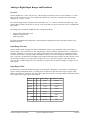
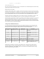
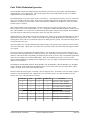
Data Acquisition
The board provides the following data acquisition capabilities.
Type of I/O
Analog Input
Analog Output
Digital I/O
Counter/Timers
Characteristics
32 single-ended/16 differential inputs,16-bit resolution
Four analog outputs, 12-bit resolution
40 programmable digital I/O, 3.3V and 5V logic compatible
One 24-bit counter/timer for A/D sampling rate control
One 16-bit counter/timer for user counting and timing
functions
Standard Peripherals
The board provides the following standard system peripherals.
Peripheral
Serial ports
Four serial ports
PS/2 ports
Keyboard and mouse
USB ports
Four USB 1.1 function ports
IrDA
IDE ports
Characteristics
One IrDA 1.0
One 44-pin connector for FlashDisk
One 40-pin dual-channel UDMA-100
Compact flash socket
Serial ports 1 and 2 are derived from the South Bridge chip. Serial ports 3 and 4 are derived from an Exar 16C2850
UART chip on the ISA bus.
Serial ports 3 and 4 also can be BIOS-selected for RS-485 or RS-232. These settings can be overridden by a jumper
to select RS422. Termination resistors of 120 ohms can be jumper-enabled on these two ports.
Console redirection feature is incorporated. This feature enables keyboard input and character video output to be
routed to one of the serial ports.
The board contains provision for mounting a solid state IDE flashdisk module with capacities ranging from 32MB
and greater. The module mounts onto the board using a 44-pin 2mm pitch header and a hold-down mounting hole
with spacer and screws.
A compact flash socket is attached to the bottom of the PCBA.
Bus Interfaces
Diamond Systems Corporation
Hercules II-EBX User Manual
Page 12
The PCI bus is the primary connection between the North Bridge, South Bridge, Ethernet, and PC/104-Plus devices.
The ISA bus is exposed on PC/104 connectors for use by add-on modules. The PC/104 connectors allow expansion
above the board only.
Power Supply
The power supply is an on-board converter, allowing an input range of 5 to 28VDC. Jumper selection allows power
to be taken from the PC-104 bus and not from the on-board converter.
The power supply includes ATX power switching and ACPI power management support. The master +5V input is
controlled by the ATX function with an external switch input.
Battery Backup
The board includes a backup battery for CMOS RAM and real-time clock backup. The battery life is greater than
four years. A connector and jumper are provided to disable the on-board battery and enable the use of an external
battery, instead.
Watchdog Timer
A watchdog timer (WDT) circuit consists of two cascaded programmable timers, which may be triggered in
hardware or software.
Configurations
Hercules II EBX is available in two standard configurations. (Custom configurations and ruggedization services are
also available).
Model
HRC800-5A512
Description
800MHz processor, 512MB DRAM, full data acquisition
HRC800-5N256
800MHz processor, 256MB DRAM, digital I/O
Diamond Systems Corporation
Hercules II-EBX User Manual
Page 13
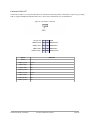
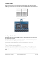
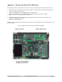
Board Description
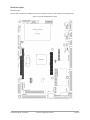
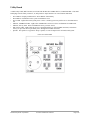
Board Layout
Figure 2 shows the Hercules II EBX board layout, including connectors, jumper blocks and mounting holes.
Figure 2: Hercules II EBX Board Layout
Diamond Systems Corporation
Hercules II-EBX User Manual
Page 14
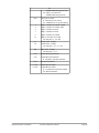
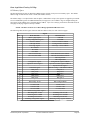
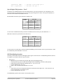
Connector Summary
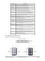
The following table lists the connectors on the Hercules II EBX board.
Connector
Description
J1
PC/104, ISA bus A,B
Manufacturer Part No.
EPT 962-60323-12
J2
PC/104, ISA bus C,D
EPT 962-60203-12
J3
PC/104-Plus PCI bus connector
-
J6
PS/2 Mouse and keyboard
Digikey 640456-8
J7
Standard button/LED utility connector
Phyco 2120-20S
J8
Data acquisition digital I/O, 50-pin
Phyco 2120-50S
J9
Data acquisition analog I/O, 40-pin
Phyco 2120-40S
J10
RJ-45 Ethernet
Capsco Sales, Inc. GD-PNS-88
J11
Ethernet header
Digikey 640456-6
J12
Audio I/O
Digikey A1925
J13
Speaker
Standard 2x5, 0.1” Box header
J14
CD Input
Molex 70543-0003
J15
External auxiliary power (output)
Digikey 640456-4
Primary IDE
All American Semiconductor
2115-2X22GDP/PPTB
Secondary IDE
Phyco 2120-40S
(with pin 20 removed)
J18
RS232/RS485/RS422 serial I/O
Phyco 2120-40S
J20
External battery
Digikey A1921
USB 2/3 (USB 1.1)
Standard 2x5, 0.1” header
(with pin 1 removed)
USB 0/1 (USB 1.1)
Standard 2x5, 0.1” header
(with pin 1 removed)
USB1 (USB 1.1)
Capsco Sales, Inc.
KUSB-AS-1-N-WHT
LCD panel (LVDS interface)
JST Part No.:
BM30B-SRDS-G-TF
J25
VGA
Standard 2x5, 0.1” Box header
J26
Video/TV out
Digikey 640456-5
J27
CPU fan
Heilind Electronics 89400-0320
J28
LCD backlight
Digikey A19470
J29
Low-voltage power input
Digikey A1925
J30
High-voltage power input (optional)
Digikey A1921
J34
CompactFlash slot (on bottom of board)
-
J36
Non-functional
Standard 2x5, 0.1” header
(with pin 1 removed)
Non-functional
Standard 2x5, 0.1” header
(with pin 1 removed)
J16
J17
J21
J22
J23
J24
J37
Diamond Systems Corporation
Hercules II-EBX User Manual
Page 15
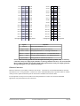
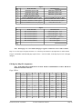
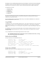
Jumper Summary
The following table lists the jumpers on the board.
Jumper
Description
J4
Serial port and A/D IRQ settings
ATX power control
Erasing CMOS RAM
RS-485 termination settings
RS-422 termination and selection
J5
Serial port address setting
CompactFlash IDE control
Write-protect BIOS flash
DIO pull-up/pull-down selections
J19
PCI VI/O voltage selection
J35
Crisis recovery
Diamond Systems Corporation
Hercules II-EBX User Manual
Page 16
Connectors
This section describes the connectors on the Hercules II EBX board.
Note: All cables mentioned in this section are included in Diamond Systems Corporation cable kit
C-HRCEBX-KIT. Some cables are also available individually.
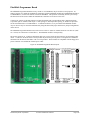
PC/104 ISA Bus
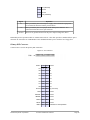
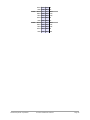
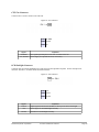
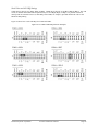
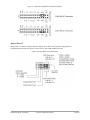
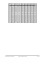
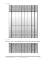
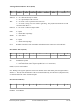
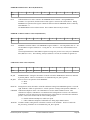
Connectors J1 and J2 carry the ISA bus signals. Figure 3 shows the PC/104 A and B pin layout for J1, and the C and
D pin layout for J2.
Figure 3: J1 and J2 Connectors
J1 Connector Pinout
IOCHCHKSD7
SD6
SD5
SD4
SD3
SD2
SD1
SD0
IOCHRDY
AEN
SA19
SA18
SA17
SA16
SA5
SA14
SA13
SA12
SA11
SA10
SA9
SA8
SA7
SA6
SA5
SA4
SA3
SA2
SA1
SA0
GND
A1
A2
A3
A4
A5
A6
A7
A8
A9
A10
A11
A12
A13
A14
A15
A16
A17
A18
A19
A20
A21
A22
A23
A24
A25
A26
A27
A28
A29
A30
A31
A32
Diamond Systems Corporation
B1
B2
B3
B4
B5
B6
B7
B8
B9
B10
B11
B12
B13
B14
B15
B16
B17
B18
B19
B20
B21
B22
B23
B24
B25
B26
B27
B28
B29
B30
B31
B32
J2 Connector Pinout
GND
RESETDRV
+5V
IRQ9
-5V
DRQ2
-12V
ENDXFR+12V
keyed
SMEMWSMEMRIOWIORDACK3DRQ3
DACK1DRQ1
REFRESHSYSCLK
IRQ7
IRQ6
IRQ5
IRQ4
IRQ3
DACK2TC
BALE
+5V
OSC
GND
GND
GND
SBHELA23
LA22
LA21
LA20
LA19
LA18
LA17
MEMRMEMWSD8
SD9
SD10
SD11
SD12
SD13
SD14
SD15
keyed
Hercules II-EBX User Manual
D0
D1
D2
D3
D4
D5
D6
D7
D8
D9
D10
D11
D12
D13
D14
D15
D16
D17
D18
D19
D0
D1
D2
D3
D4
D5
D6
D7
D8
D9
D10
D11
D12
D13
D14
D15
D16
D17
D18
D19
GND
MEMCS16-IOCS16IRQ10
IRQ11
IRQ12
IRQ15
IRQ14
DACK0DRQ0
DACK5DRQ5
DACK6DRQ6
DACK7DRQ7
+5
MASTERGND
GND
Page 17
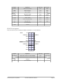
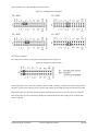
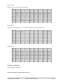
PC/104-Plus PCI Bus
The PC/104-Plus bus is essentially identical to the PCI Bus except for the physical design. A single pin and socket
connector is specified for the bus signals. A 120-pin header, J3, arranged as four 30-pin rows incorporates a full 32bit, 33MHz PCI Bus. The additional pins on the PC/104-Plus connectors are used as ground or key pins. The
female sockets on the top of the board enable stacking another PC/104-Plus board on top of the Hercules II EBX
board. The Hercules II EBX board should be the bottom board of a PC/104-Plus stackup.
In the connector J3 pinout table, below, the top corresponds to the left edge of the connector when the board is
viewed from the primary side (the side with the CPU chip and the female end of the PC/104-Plus connector), and
the board is oriented so that the PC/104 connectors are along the bottom edge of the board and the PC/104-Plus
connector is in the center of the Hercules II EBX board.
Figure 4: J3 Connector
1
2
3
4
5
6
7
8
9
10
11
12
13
14
15
16
17
18
19
20
21
22
23
24
25
26
27
28
29
30
A
GND/5.0V KEY
VI/O
AD05
C/BE0*
GND
AD11
AD14
+3.3V
SERR*
GND
STOP*
+3.3V
FRAME*
GND
AD18
AD21
+3.3V
IDSEL0
AD24
GND
AD29
+5V
REQ0*
GND
GNT1*
+5V
CLK2
GND
+12V
-12V
Diamond Systems Corporation
B
Reserved
AD02
GND
AD07
AD09
VI/O
AD13
C/BE1*
GND
PERR*
+3.3V
TRDY*
GND
AD16
+3.3V
AD20
AD23
GND
C/BE3*
AD26
+5V
AD30
GND
REQ2*
VI/O
CLK0
+5V
INTD*
INTA*
Reserved
C
+5V
AD01
AD04
GND
AD08
AD10
GND
AD15
SB0*
+3.3V
LOCK*
GND
IRDY*
+3.3V
AD17
GND
AD22
IDSEL1
VI/O
AD25
AD28
GND
REQ1*
+5V
GNT2*
GND
CLK3
+5V
INTB*
Reserved
Hercules II-EBX User Manual
D
AD00
+5V
AD03
AD06
GND
M66EN
AD12
+3.3V
PAR
SDONE
GND
DESEL*
+3.3V
C/BE2*
GND
AD19
+3.3V
IDSEL2
IDSEL3
GND
AD27
AD31
VI/O
GNT0*
GND
CLK1
GND
RST*
INTC*
GND/3.3V KEY
Page 18
The PCI board interface is designed to allow different voltage levels for the signaling interface. The keying
mechanism defined by the specification is intended to prevent a 3.3V-only device that is not 5V tolerant from
receiving signals that are at a 5V signal rail. In a standard PCI interface, this is handled by blocking a portion of the
edge connector such that the female connector is keyed as either “3.3V” or “5V”. This is intended to provide a way
of preventing a 3.3V-only card in a 5V system. Many vendors choose to implement a “universal” edge connector
that fits into either configuration; this is typically done in one of two ways:
•
•
Use 3.3V signaling that is 5V-tolerant.
Use the VIO pins on the PCI edge connector to power the I/O drive circuitry (or the maximum voltage
overshoot protection circuitry) on the card.
From a system perspective, the primary question is, which standard can you support? Many card vendors choose to
implement a specific standard, such as “5V only,” and connect the VIO signals to the internal power rail, such as
“5V” signals on the PCI edge connector. While this is a violation of the more recent PCI specification, it is also
relatively common, especially for card developers who developed PCI cards before the standard was updated for
3.3V support.
On the Hercules II EBX, all of the PCI circuitry is driven with 3.3V circuitry and is 5V tolerant. Given this, the
Hercules II EBX main board can support either 3.3V or 5V-only cards. For this reason, the connector is not keyed
(to prevent certain types of cards from being inserted). Rather, the main EBX board allows you to select which I/O
voltage to use for a given PC/104-Plus card, or set of cards.
Many PC/104-Plus cards are universal, in which case the voltage setting does not matter, provided that it is set to
either 3.3V or 5V. For cards that have a definite requirement, set the VIO jumper, J19, to the appropriate position.
According to the specification, a 5V-only card can be recognized by the keying position at location A1, where a
male pin A1 cut and a female location A1 is be blocked).
Similarly, cards that are to have 3.3V power should have pin D30 cut and female location D30 plugged.
Cards without either keying mechanism are “universal” and operate with either, 3.3V or 5V, I/O voltage.
Note: Do not mix cards that have different I/O keying requirements; i.e., do not stack a card that has
pin A1 cut with a card that has pin D30 cut.
Diamond Systems Corporation
Hercules II-EBX User Manual
Page 19
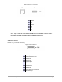
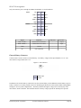
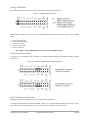
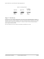
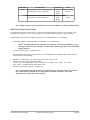
PS2 Mouse and Keyboard connector
Connector J6 is used to connect a mouse or keyboard. This connector mates with Diamond Systems Corporation
cable no. 698022, which terminates the cable to two PS/2 Female connectors.
Figure 5: J6 Connector
1
+5vin (keyboard PS/2 pin 4)
2
Keyboard data (keyboard PS/2 pin 1)
3
Keyboard clock (keyboard PS/2 pin 5)
4
Ground (keyboard PS/2 pin 3)
5
+5v in (mouse PS/2 pin 4
6
Mouse data (mouse PS/2 pin 1)
7
Mouse clock (mouse PS/2 pin 5)
8
Ground (mouse PS/2 pin 3)
Note: Pins 2 and 6 on the Mini-Din-6 PS/2 connectors are unused.
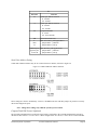
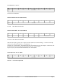
Utility Connector
Connector J7 provides access to the standard button/LED connections.
Figure 6: J7 Connector
Ground
1
2
Reset key
Ground
3
4
ATX power button
Network activity LED
5
6
+3.3v standby
Network 100 Mbit link
7
8
+3.3v standby
+5v in
9
10
IDE LED
Power LED
11
12
External battery
Watchdog timer - input
13
14
Ground
Speaker
15
16
Watchdog timer - output
+5v in
17
18
IRTX (IR transmit)
IRRX (IR receive)
19
20
Ground
Diamond Systems Corporation
Hercules II-EBX User Manual
Page 20
Signal
Reset key
ATX power button
Definition
Connection between Reset key and ground generate a reset condition. The board
remains in a reset state (with non-standby power rails disabled) until Reset key is
removed from ground.
The ATX power button should be tied to ground whenever the “Power Button” is used.
The “Power Button” has different functionality, depending on the current system mode
and software operation. In general, the following guidelines apply.
•
If the board is powered down, toggling (i.e., tie to ground briefly, then release) this
button turns the system on, causing all non-standby voltages to become active.
NOTE: depending on the default configuration, the system usually powersup immediately as power is applied.
•
•
If the system is currently powered up and active, toggling (i.e., tie to ground briefly,
then release) this button causes a system power-down event to be initiated.
Typically, this powers-down the monitor, hard drive, and any other non-essential
functions. The system must be operating and the software executing normally for
this function. Under Windows and some other OSs, this power-down event may
cause the system to shut down. Typically, this is software-configurable via an
option setting for the given OS.
If the system is currently powered-up and active, holding this button for four
seconds causes a forced system shutdown. This is a hardware power-down, which
can be detrimental to many OSs due to the fact that they are not given adequate time
to initiate shut-down sequencing. This operation should only be used in critical
circumstances, such as when the system itself is locked due to system instability or a
software crash. After powering the system down in this manner, the system remains
powered down until the power button is toggled (tied to ground again and released).
When ATX is enabled, a momentary contact between this pin and Ground causes the
CPU to turn on and a contact of four seconds or longer generates a power shutdown.
ATX power control is enabled using a jumper on jumper block J4.
+5v in
The +5v pin is a switched power pin that is turned on and off with either the ATX power
switch or the +5v input.
+3.3v standby
The +3.3V standby pin provides a special “standby voltage” regardless of system powerdown mode. This voltage is present whenever the system has power connected,
regardless of the current system power-down state. This voltage is not intended as a
major power-source for external devices. Instead, it is intended to allow external display
of current system power status. This power supply should not be used unless absolutely
necessary, in which case it should only be used as a source for LED display or similar
power draw.
Network activity LED
The Network activity LED pin provides a signal that is the same as the LED marked
“ACT” on the main board. It lights during receive or transmit activity on the Ethernet
connection. An LED should be tied between power and this pin.
Network 100 Mbit link The Network 100Mbit link pin provides a signal that is the same as the LED marked
“100” on the main board. It lights whenever a 100MBit Ethernet link is established. An
LED should be tied between power and this pin.
IDE LED
Power LED
Speaker
The IDE LED is referenced to +5V out and requires a series resistor. Connect the LED
directly between this pin and resistor (to +5V).
The Power LED referenced to +5V out does not require a series resistor. Connect the
LED directly between this pin and +5V Out. Note that this displays the system main
power. If the system is in a power-down mode, this LED may be inactive while the
system is still receiving power to its standby voltage sources.
The signal on the Speaker pin is referenced to +5V out. Connect a speaker between this
pin and +5V out.
Diamond Systems Corporation
Hercules II-EBX User Manual
Page 21
Signal
IRTX
Definition
The IR Receive/Transmit pins are used for IrDA functions. They should be connected
to an external IrDA transceiver when needed. IR communications require that COM
PORT 2 be set for “IR” mode for the IR serial port functionality to be active.
External battery
The External battery pin is an additional power connection for an external +3V power
source, in addition to connector J20. Note that these two sources are not directly
connected and may both be driven by separate external battery power sources. Typical
power draw from this battery source averages under 4uA of current.
Watchdog timer
The Watchdog input/output signals are signals are used in conjunction with the on-board
FPGA and Data Acquisition circuitry to provide full watchdog timer functionality.
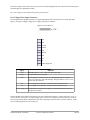
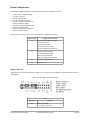
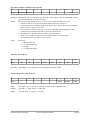
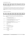
Data Acquisition (Digital I/O) Connector
Hercules II EBX includes a 50-pin header, J8, for all digital data acquisition I/O. This header is located on the right
side of the board. Pin 1 is the lower right pin, as marked on the board. Diamond Systems Corporation cable no. C50-18 provides a standard 50-pin connector at each end and mates with this header.
Figure 7: J8 Connector
Diamond Systems Corporation
DIO A0
1
2
DIO A1
DIO A2
3
4
DIO A3
DIO A4
5
6
DIO A5
DIO A6
7
8
DIO A7
DIO B0
9
10
DIO B1
DIO B2
11
12
DIO B3
DIO B5
13
14
DIO B5
DIO B6
15
16
DIO B7
DIO C0
17
18
DIO C1
DIO C2
19
20
DIO C3
DIO C4
21
22
DIO C5
DIO C6
23
24
DIO C7
DIO D0
25
26
DIO D1
DIO D2
27
28
DIO D3
DIO D4
29
30
DIO D5
DIO D6
31
32
DIO D7
DIO E0/PWM0
33
34
DIO E1/PWM1
Hercules II-EBX User Manual
Page 22
Diamond Systems Corporation
DIO E2/PWM2
35
36
DIO E3/PWM3
DIO E4/GATE1
37
38
DIOE5/TOUT1
DIO E6/DIOLATCH
39
40
DIO E7/GATE0
EXTTRIG
41
42
TOUT0
ACK
43
44
WDI
WDO
45
46
FXA
FXB
47
48
FXB
+5v
49
50
Digital ground
Hercules II-EBX User Manual
Page 23
Signal
DIO A7-A0
Definition
Digital I/O port A; programmable direction
DIO B7-B0
Digital I/O port B; programmable direction
DIO C7-C0
Digital I/O port C; programmable direction
DIO D7-D0
Digital I/O port D; programmable direction
DIO E7-E0
Digital I/O port E; programmable direction
Note : E3-E0 may be configured for PWM signals.
PWM3-PWM0 Pulse-Width Modulation Outputs (4 independent channels)
Note : E7-E4 may be configured for counter/timer signals.
GATE 1-0
Gate inputs for Counter/Timer 1 and 0
TOUT1
Counter/Timer 1 output
DIOLATCH
Ext Trig
Handshaking line used (with ACK signal below) for
automated digital data transfers
External A/D trigger input, External Counter/Timer 1 input
Tout 0
Counter/Timer 1 output
+5V Out
Connected to switched +5V supply (output only! Do not
connect to external supply)
Digital Ground Digital ground (0V - reference); used for digital circuitry only
WDO
Watchdog Timer Output
NOTE: The watchdog timer circuit may be programmed
directly or with Diamond Systems’ Universal Driver software.
WDI
Watchdog Timer Input
NOTE: The watchdog timer circuit may be programmed
directly or with Diamond Systems’ Universal Driver software.
ACK
Handshaking line used (with DIOLATCH signal) for
automated digital data transfers
FXA, FXB
These lines should be left unconnected
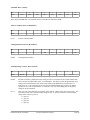
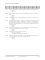
Data Acquisition (Analog I/O) Connector
Connector J9 is used for analog I/O data acquisition.
Figure 8: J9 Connector
Single-ended
Differential
Vout 0
1
2
Vout 1
Vout 0
1
2
Vout 1
Vout 2
3
4
Vout 3
Vout 2
3
4
Vout 3
Output ground
5
6
Output ground
Output ground
5
6
Output ground
Vin 0
7
8
Vin 16
Vin 0 +
7
8
Vin 0 -
Vin 1
9
10
Vin 17
Vin 1 +
9
10
Vin 1 -
Diamond Systems Corporation
Hercules II-EBX User Manual
Page 24
Vin 2
11
12
Vin 18
Vin 2 +
11
12
Vin 2 -
Vin 3
13
14
Vin 19
Vin 3 +
13
14
Vin 3 -
Vin 4
15
16
Vin 20
Vin 4 +
15
16
Vin 4 -
Vin 5
17
18
Vin 21
Vin 5 +
17
18
Vin 5 -
Vin 6
19
20
Vin 22
Vin 6 +
19
20
Vin 6 -
Vin 7
21
22
Vin 23
Vin 7 +
21
22
Vin 7 -
Vin 8
23
24
Vin 24
Vin 8 +
23
24
Vin 8 -
Vin 9
25
26
Vin 25
Vin 9 +
25
26
Vin 9 -
Vin 10
27
28
Vin 26
Vin 10 +
27
28
Vin 10 -
Vin 11
29
30
Vin 27
Vin 11 +
29
30
Vin 11 -
Vin 12
31
32
Vin 28
Vin 12 +
31
32
Vin 12 -
Vin 13
33
34
Vin 29
Vin 13 +
33
34
Vin 13 -
Vin 14
35
36
Vin 30
Vin 14 +
35
36
Vin 14 -
Vin 15
37
38
Vin 31
Vin 15 +
37
38
Vin 15 -
Input ground
39
40
Input ground
Input ground
39
40
Input ground
Signal
Vout3-0
Definition
Analog output channels 3 – 0
Output Ground
Analog ground; 0V reference for VOut3-0
Vin 31 ~ Vin 0
Analog input channels 31 – 0 in single-ended mode
Vin 15 + ~ Vin 0 + High side of input channels 15 – 0 in differential mode
Vin 15 - ~ Vin 0 - Low side of input channels 15 – 0 in differential mode
Input Ground
Analog ground; 0V reference for VIn31-0
NOTE: These reference grounds are NOT decoupled from the power grounds – they are indirectly
connected to the power supply input (and other on-board ground/0V references). Do not assume that
these grounds are floating; do not apply a high-voltage input (relative to the power input ground) to
these ground signals or to any other board I/O pin.
Ethernet Connectors
Ethernet connectivity is provided by connectors J10 and J11. Connector J10 is a board mounted RJ-45 connector
and connector J11 is a 1x6 pin header. Connector J11 mates with Diamond Systems Corporation cable no. 698002,
which provides a panel-mount RJ-45 jack for connection to standard CAT5 network cables.
For development, J10 may be more useful but it is anticipated that J11 will be more useful for embedded
applications (for panel-mount network connection).
Diamond Systems Corporation
Hercules II-EBX User Manual
Page 25
Figure 9: J10 and J11 Connectors
1
Common
2
RX-
3
Common
4
RX+
5
TX-
6
TX+
Note: Only one of the J11 or J10 connectors should be used at a time. Both connectors are NOT
independent and neither will function if both are simultaneously connected.
Audio I/O Connector
Connector J12 provides audio connectivity.
Figure 10: J12 Connector
Diamond Systems Corporation
1
Left headphone/Line out
2
Right headphone/Line out
3
Audio ground
4
Left line input
5
Right line input
6
left AUX input
7
Right AUX input
8
Audio ground
9
power reference for microphone
10
Microphone input
Hercules II-EBX User Manual
Page 26
Signal
Definition
Headphone/Line Out Line Level output, capable of driving headphones, which is referred to
as “Headphone Out” in most sound documentation.
Line Input
Line-Level input, which is referred to as “Line In” in most sound
documentation.
Auxiliary Input
Line-Level input, which is referred to as “AUX In” in most sound
documentation.
Microphone Input
Microphone-level mono input; phantom power provided via pin 9.
The Hercules II EBX sound chip is AC97-compatible. The “Line Out” is powered and used for the amplified
Speaker Connector output, J13, described below. The line-level output listed above is listed as either “Headphone
Out” or “Line Out 2” in most of the software and documentation for this sound interface.
Speaker Connector
Connector J13 is used to connect speakers.
Figure 11: J13 Connector
Signal
Speaker LEFT +/Speaker RIGHT +/Mono Output
1
Speaker left high (+)
2
Volume - low
3
Speaker left low (-)
4
Volume - mid
5
Line level mono output
6
Audio ground
7
Speaker right low (-)
8
Volume - high
9
Speaker right high (+)
10
No-connect
Definition
Speaker Connection Pair for LEFT speaker (4-Ohm Speaker)
Speaker Connection Pair for RIGHT speaker (4-Ohm Speaker)
Line-Level mono output (for reference)
Volume – LOW, MID, HIGH These are volume controls for the attached speakers
Diamond Systems Corporation
Hercules II-EBX User Manual
Page 27
The volume control is capable of 32 discrete levels, ranging from a 20dB maximum gain to -85dB (Muted). The
main volume control is the “MID” line, which may be tied to the center tap of a potentiometer with “HIGH” on one
side and “LOW” on the other to give a full range of power control.
•
•
•
Shorting “MID” to “LOW” mutes the speaker audio.
Shorting “MID” to “HIGH” provides maximum gain.
Default (no connection) provides 10dB of gain.
The maximum output power is specified to provide up to two Watts into a 4-Ohm speaker load. Note that this
output power is drawn from the on-board 5V supply.
The speakers are driven using a Bridged-Tied Load (BTL) amplifier configuration. This is a differential speaker
connection. As such, each speaker should be wired directly to the appropriate pair of connections for that speaker.
•
•
Do not connect the speaker low sides (-) to ground
Do not short the speaker low connections together.
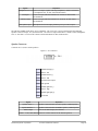
CD Input Connector
Connector J14 provides a connector for a PC-standard CD input cable.
Figure 12: J14 Connector
1
Left CD input
2
Left ground
3
Right ground
4
Right CD input
J14 provides the CD Audio Input to the AC97 Sound circuitry. The connector is an industry-standard CD-IN
connector, which is common in most desktop Personal Computers. Note that the left and right grounds are
decoupled but are also tied together on-board. This input is intended for CD-input only (i.e., no amplified or
microphone inputs).
External Auxiliary Power Connector (Output)
Connector J15 provides switched power for use with external drives. If ATX is enabled, the power is switched ON
and OFF with the ATX input switch. If ATX is not enabled, the power is switched ON and OFF in conjunction with
the external power.
Figure 13: J15 Connector
Diamond Systems Corporation
Hercules II-EBX User Manual
Page 28
Signal
+5v
1
+5v (switched)
2
Ground
3
Ground
4
+12v (switched)
Definition
This is provided by the on-board power supply, derived from the input power.
It is switched off when the board is powered down.
+12v
This is provided by the 12V input pin on the main power connector. It is
switched off when the board is powered down.
Ground
These are 0V ground references for the power output voltage rails, above.
Diamond Systems Corporation cable no. 698006 mates with J15. This cable provides a standard full-size power
connector for a hard drive or CD-ROM drive and a standard miniature power connector for a floppy drive.
Primary IDE Connector
Connector J16 is used for the primary IDE connection.
Figure 14: J16 Connector
Diamond Systems Corporation
Reset -
1
2
Ground
D7
3
4
D8
D6
5
6
D9
D5
7
8
D10
D4
9
10
D11
D3
11
12
D12
D2
13
14
D13
D1
15
16
D14
D0
17
18
D15
Ground
19
20
Key (not used)
DRQ
21
22
Ground
IDEIOW-
23
24
Ground
IDEIOR-
25
26
Ground
IORDY
27
28
Ground
DACK-
29
30
Ground
IRQ14
31
32
Pulled low for 16-bit operation
Hercules II-EBX User Manual
Page 29
A1
33
34
Not used
A0
35
36
A2
CS0-
37
38
CA1-
LED-
39
40
Ground
+5v
41
42
+5v
Ground
43
44
Not used
Connector J16 mates with Diamond Systems Corporation cable no. 698004, and may be used to connect up to two
IDE drives (hard disks, CD-ROMs, or flash disk modules). The 44-pin connector includes power and mates directly
with notebook drives and flash disk modules. To use a standard format hard disk or CD-ROM drive with a 40-pin
connector, an adapter PCB such as Diamond Systems Corporation ACC-IDEEXT is required.
Note: Connector J16 supports only up to ATA-33 (UDMA-2). It does not support ATA-66 (UDMA3 to 5) transfer modes.
Secondary IDE Connector
Connector J17 is used for the secondary IDE connection.
Figure 15: J17 Connector
Diamond Systems Corporation
Reset -
1
2
Ground
D7
3
4
D8
D6
5
6
D9
D5
7
8
D10
D4
9
10
D11
D3
11
12
D12
D2
13
14
D13
D1
15
16
D14
D0
17
18
D15
Ground
19
20
Key (not used)
DRQ
21
22
Ground
IDEIOW-
23
24
Ground
IDEIOR-
25
26
Ground
IORDY
27
28
Ground
DACK-
29
30
Ground
IRQ14
31
32
Pulled low for 16-bit operation
A1
33
34
Not used
Hercules II-EBX User Manual
Page 30
A0
35
36
A2
CS0-
37
38
CA1-
LED-
39
40
Ground
Connector J17 mates with Diamond Systems Corporation UDMA cable no. 698026, and may be used to connect up
to two IDE drives (hard disks, CD-ROMs or other IDE/ATAPI devices). The 40-pin connector must mate with this
80-conductor UDMA cable for maximum performance. Connector J17 fully supports up to ATA-100 (UDMA
Mode 5), provided that an appropriate UDMA (80-conductor) cable is used.
Note: The cable type is automatically be detected by the BIOS and the transfer speed is limited as
necessary.
Serial Port I/O Connector
Connector J18 is a 40-pin header that provides access to the four on-board serial ports. The PORT1 and PORT2
serial ports are always configured for RS-232. The PORT3 and PORT4 serial ports are software configurable as
either RS-232, RS-485 or RS-422. All four serial ports are independently enabled. The last two serial ports can be
independently configured between the RS-232, RS-485 and RS-422 modes of operation.
Figure 16: J18 Connector
Port No.
PORT1
Pin Assignment
Pins 1 - 10
PORT2
Pins 11 - 20
PORT3
Pins 21 - 30
PORT4
Pins 31 - 40
Diamond Systems Corporation Cable Assembly Number C-DB9M-4 connects this header to four DE-9 Male
connectors, for direct connection to RS-232-C signaling. The following tables list the signals for the appropriate
mode of operation, as well as the DE-9 pin numbers to which these signals are wired.
RS-232 Pin Assignment
COM1:
COM2:
Diamond Systems Corporation
DCD1
1
2
DSR1
RXD1
3
4
RTS1
TXD1
5
6
CTS1
DTR1
7
8
RI1
GND
9
10
N/C
DCD2
11
12
DSR2
RXD2
13
14
RTS2
TXD2
15
16
CTS2
Hercules II-EBX User Manual
Page 31
COM3:
COM4:
Diamond Systems Corporation
DTR2
17
18
RI2
GND
19
20
N/C
DCD3
21
22
DSR3
RXD3
23
24
RTS3
TXD3
25
26
CTS3
DTR3
27
28
RI3
GND
29
30
N/C
DCD4
31
32
DSR4
RXD4
33
34
RTS4
TXD4
35
36
CTS4
DTR4
37
38
RI4
GND
39
40
GND
Hercules II-EBX User Manual
Page 32
Signal
DCDn
Definition
Data Carrier Detect
DE-9 Pin
pin 1
Direction
Input
DSRn
Data Set Ready
pin 6
Input
RXDn
Receive Data
pin 2
Input
RTSn
Request to Send
pin 7
Output
TXDn
Transmit Data
pin 3
Output
CTSn
Clear to Send
pin 8
Input
DTRn
Data Terminal Ready
pin 4
Output
RIn
Ring Indicator
pin 9
Input
NC
(not connected)
-
-
GND
Ground
-
-
RS-485 Pin Assignment
Only J18 connector pins 21 through 40, PORT3 and PORT4, are used for RS-485.
COM3:
COM4:
NC
21
22
NC
TXD/RXD+3
23
24
TXD/RXD-3
GND
25
26
NC
NC
27
28
NC
GND
29
30
DIOC
NC
31
32
NC
TXD/RXD+4
33
34
TXD/RXD-4
GND
35
36
NC
NC
37
38
NC
GND
39
40
DOI
Signal
TXD/RXD+n
Definition
Differential Transceiver Data (HIGH)
DE-9 Pin
pin 2
Direction
bi-directional
TXD/RXD-n
Differential Transceiver Data (LOW)
pin 7
bi-directional
GND
Ground
-
-
NC
(not connected)
-
-
Diamond Systems Corporation
Hercules II-EBX User Manual
Page 33
RS-422 Pin Assignment
Only J18 connector pins 21 through 40, PORT3 and PORT4, are used for RS-422.
COM3:
COM4:
NC
21
22
NC
TXD+1
23
24
TXD-1
GND
25
26
RXD-1
RXD+1
27
28
NC
GND
29
30
NC
NC
31
32
NC
TXD+2
33
34
TXD-2
GND
35
36
RXD-2
RXD+2
37
38
NC
GND
39
40
NC
Signal
TXD+n/TXD-n
Definition
Differential transmit data
DE-9 Pin
-
Direction
Output
RXD+n/RXD-n
Differential receive data
-
Input
GND
Ground
-
-
NC
(not connected)
-
-
External Battery Connector
Connector J20 is used to connect an external battery. The battery voltage for this input should be 3-3.5V. The
current draw averages under 4uA at 3V.
Figure 17: J20 Connector
1
Battery input
2
Ground
In addition to the external battery connected to J20, the on-board battery and an additional external battery input on
Utility Connector J7 are other possible sources for maintaining the Real-Time Clock and the CMOS settings (BIOS
settings for various system configurations). The battery that has the highest voltage will see the majority of the
current draw, which is minimal. Note that there must be a battery voltage input for the default power-up mode.
Diamond Systems Corporation
Hercules II-EBX User Manual
Page 34
USB 1.1 Connectors
Connectors J21 and J22 are used to connect USB 2/3 and USB 0/1, respectively, and support USB 1.1 with 10Mbps
maximum data transfer rates.
Figure 18: J21 and J22 Connectors
Signal
Shield
Key (pin cut)
1
2
Shield
USB1/3 power-
3
4
USB0/2 power-
USB1/3 data+
5
6
USB0/2 data+
USB1/3 data-
7
8
USB0/2 data-
USB1/3 power+
9
10 USB0/2 power+
Definition
-
USB0/2 power-
ground
USB0/2 data+
data +
USB0/2 data-
data -
USB0/2 power+
+5V
USB1/3 power-
ground
USB1/3 data+
data +
USB1/3 data-
data -
USB1/3power+
+5V
Connectors J21 and J22 mate with Diamond Systems Corporation cable no. 698012, which provides two standard
USB type A jacks in a panel-mount housing.
Note: USB1, described below, shares the J22 USB circuitry. Do not connect USB devices to both
USB1, on J23, and J22.
Diamond Systems Corporation
Hercules II-EBX User Manual
Page 35
USB1 Connector
Connector J23 provides a single, quick and simple on-board USB connection for simple test and development
without requiring an additional cable.
Figure 19: J23 Connector
Signal
power-
ground
data+
data +
data-
data -
power+
+5V
1
power+
2
data-
3
data+
4
power-
Definition
Note: USB1 shares the J22 USB circuitry. Do not connect USB devices to both USB1 and J22.
Diamond Systems Corporation
Hercules II-EBX User Manual
Page 36
LCD Panel (LVDS Interface) Connector
Connector J24 provides access to the internal LVDS LCD display drivers. Note that the LCD also requires the
backlight to be connected (J28 below) to function correctly.
Ground
1
2
Ground
Y clock-
3
4
Z clock-
Y clock+
5
6
Z clock+
Ground
7
8
Ground
Y data 0-
9
10
Z data 0-
Y data 0+
11
12
Z data 0+
Ground
13
14
Ground
Y data 2-
15
16
Z data 1-
Y data 2+
17
18
Z data 1+
Ground
19
20
Ground
Y data 1-
21
22
Z data 2-
Y data 1+
23
24
Z data 2+
Ground
25
26
Ground
VDD (LDC display)
27
28
VDD (LCD display)
VDD (LDC display)
29
30
VDD (LCD display)
Signal
Definition
Y Data 2-0 +/- Primary Data Channel, bits 2-0 (LVDS Differential signaling)
Y Clock +/-
Primary Data Channel, Clock (LVDS Differential signaling)
Z Data 2-0 +/- Secondary Data Channel, bits 2-0 (LVDS Differential signaling)
Z Clock +/VDD
Ground
Secondary Data Channel, Clock (LVDS Differential signaling)
+3.3V Switched Power Supply for LCD display (only powered up when
LCD display is active)
Power Ground, 0V
Diamond Systems Corporation
Hercules II-EBX User Manual
Page 37
VGA Connector
Connector J25 provides a connection for VGA monitors.
Figure 20: J25 Connector
Signal
RED
R-Ground
GREEN
G-Ground
BLUE
B-Ground
Red
1
2
R-ground
Green
3
4
G-ground
Blue
5
6
B-ground
HSYNCH
7
8
DDC data
VSYNCH
9
10
DDC clock
Definition
RED signal (positive, 0.7Vpp into 75 Ohm load)
Ground return for RED signal
GREEN signal (positive, 0.7Vpp into 75 Ohm load)
Ground return for GREEN signal
BLUE signal (positive, 0.7Vpp into 75 Ohm load)
Ground return for BLUE signal
DDC-CLOCK/DATA Digital serial I/O signals used for monitor detection (DDC1 specification)
Diamond Systems Corporation Cable Assembly #698024 provides a female DB15 connection to interface with a
standard RGB monitor.
Note: While the DDC serial detection pins are present, a 5V power supply is not provided (the old
“Monitor ID” pins are also not used).
Diamond Systems Corporation
Hercules II-EBX User Manual
Page 38
Video/TV Out Connector
Connector J26 provides a video output for connection to a standard (NTSC) TV. Either S-Video (6-pin mini-DIN)
or Composite (RCA Jack) can be used, but not both.
Figure 21: J26 Connector
1
S video Y
2
S video C
3
Composite
4
Ground
5
NC
Signal
S-Video “Y”
Definition
S-Video “Brightness” (Luminance)
S-Video “C”
S-Video “Color” (Chrominance)
Composite
Ground
NC
Composite Video
Ground (for either S-Video or Composite)
Do not connect this signal; For testing use only
Notes:
•
This feature requires software support to function, and is not directly supported in the BIOS.
•
LCD, S-Video, and Composite are mutually-exclusive. It is not possible to have more than one of
these options active at the same time.
Diamond Systems Corporation
Hercules II-EBX User Manual
Page 39
CPU Fan Connector
Connector J27 is used to connect to the CPU fan.
Figure 22: J27 Connector
Signal
Fan RPM
+5V, Ground
1
Fan RPM
2
Ground
3
+5v
Definition
TTL signal input that pulses with each revolution of the fan.
Power Supply for optional CPU Fan, if necessary.
LCD Backlight Connector
Connector J28 provides the backlight power and control for the optional LCD panel. See the description for
connector J24, above, for details on the LCD data interface.
Figure 23: J28 Connector
Signal
Control
+12V
Ground
1
+12v
2
Control
3
Ground
Definition
Output signal (from Hercules II EBX) to allow power-down of backlight
Power supply for LCD Backlight assembly
Ground for LCD Backlight assembly
Diamond Systems Corporation
Hercules II-EBX User Manual
Page 40
The control signal is used to allow the system to power-down the backlight when the system enables monitor-powerdown during power management control.
The +12V supply is removed when the system is powered down.
Low-Voltage Power Input Connector
The standard Hercules II EBX input power is supplied through the J29 connector from an external mid-range
supply. (An option for higher-voltage power supply input may be available).
Figure 24: J29 Connector
1
+Vin
2
+Vin
3
Ground
4
Ground
5
+12v
6
Ground
7
+Vin
8
-12v
9
-5v
10
Power supply ON
Signal
+Vin
Definition
Main input power; +5V to +28V (optional) input range.
Ground
0-V (ground) power return path.
+12V
Power supply for in-board 12V devices, including hard drives, auxiliary
power, PC/104 power, and LCD backlight. Range should be 11.9V to 13.5V
measured at this connector.
-12V
Power supply for PC/104-Plus -12V devices (no on-board devices).
-5V
Power supply for PC/104-Plus -5V devices (no on-board devices).
Power Supply ON Feedback pin for external ATX supply, when needed; pulled low when onboard power is inactive.
Hercules II EBX in the standard, mid-range power input configuration supports a voltage range from +4.75V to
+28V, with some restrictions. For input voltages from +4.75V to 6V, measured at J29, the function of some 5V
devices may be affected due to high-current draw and voltage dips encountered due to current variations. In this
case, the following behavior may be observed.
Diamond Systems Corporation
Hercules II-EBX User Manual
Page 41
•
•
•
•
•
•
Hard drives attached to the system may not power up correctly and/or may reset.
Hard drives, CD-ROMs, and other high-power devices may also draw too much power at these low voltages,
causing the system to reset. External power supplies for high-power devices are strongly recommended when
the input supply is likely to be this low.
PS/2 and USB devices may function erratically or not at all at low input voltages. An external powered USB
hub may alleviate this problem somewhat; this includes USB keyboards, mice, and especially USB boot
devices, such as floppy drives and USB flash drives.
RS-232 range and functionality may be degraded.
Audio speaker output power may be limited.
Data acquisition accuracy may be slightly affected.
At input voltage ranges above 6V (6V to 28V), these concerns are not present. The main input voltage, “Vin,” is
used to derive all on-board voltages and power supplies via on-board switching regulators.
The “+12V” power supply input is intended for all on-board and board-controlled 12V power supplies, including the
PC/104-Plus 12V supplies, the external hard drive power supply (through connector J15, described above), and the
LCD backlight. If these devices are not used, the “+12V” input may be left unconnected.
Since the PC/104 bus includes pins for -5V and -12V, these voltages may be supplied through connector J29 if
needed and left unconnected if not needed.
The +5V and +12V voltages are controlled by the ATX power manager switches, while -5V and -12V are routed
directly to the corresponding pins on the PC/104 bus and are not controlled by the ATX function.
Make certain that your power supply has enough current capacity to drive your system. The Hercules II EBX
requires 12 to 20 Watts or more, depending on which external devices are connected to the board. This could
require over 4A on the “+Vin” line at minimum voltage inputs. In particular, many disk drives need extra current
during startup. If your system fails to boot properly or if disk accesses do not work correctly, the first thing to check
is the power supply voltage level at connector J29. Many boot-up problems are caused simply by insufficient
voltage due to excess current draw on the “+Vin” supply during initialization.
Multiple +5V and ground pins are provided for extra current carrying capacity, if needed. Each pin is rated at 3A
max (15W). For the Hercules II EBX CPU with a moderate I/O device complement (basic hard drive, key board,
mouse, USB devices, and a network PC/104-Plus card, for example), 1.4A at +13V is considered sufficient.
ATX control enables the +5V and +12V power to be switched ON and OFF with an external momentary switch. A
short press on the switch turns ON power, and holding the switch on for four seconds or longer turns OFF power
(See the Utility Header description for connector J7, above).
cable no. 698015 mates with connector J29. The cable provides ten color-coded wires with stripped and tinned
leads for connection to user-supplied power sources.
For cases where the input power supply is 12V, the “+Vin” and “+12V” input wires may be connected. In this case,
ensure that the power supply into the “+12V” does not exceed the voltage requirements for that input pin.
Diamond Systems Corporation
Hercules II-EBX User Manual
Page 42
High-Voltage Power Input Connector (Optional)
Connector J30 is used for high-voltage power input, which is optionally available for special, higher-voltage
applications. This option is intended to allow for a higher power supply input than the standard power input
provided using connector J29.
Figure 25: J30 Connector
1
Ground
2
+Vwin
Signal
+Vwin
Definition
Main input power (+13V to +40V input range).
Ground
0V (ground) power return path.
CompactFlash Slot (optional)
A CompactFlash Socket is located under the board at connector J34, immediately under connector J17. If this
socket is used, it occupies the entire secondary IDE channel. To set the CompactFlash card as an IDE MASTER, so
it is detected by the BIOS, place a jumper on connector J5, as described in the following section.
Diamond Systems Corporation
Hercules II-EBX User Manual
Page 43
Connectors J36 & J37
Connectors J36 and J37 are 2x5 pin headers that were intended for connecting USB 6/7 and USB 4/5, respectively, providing
USB 2.0 support (480Mbps maximum transfer rates). However this functionality was not implemented.
Figure 26: J36 and J37 Connectors
Signal
Shield
Key (pin cut)
1
2
Shield
USB5/7 power-
3
4
USB4/6 power-
USB5/7 data+
5
6
USB4/6 data+
USB5/7 data-
7
8
USB4/6 data-
USB5/7 power+
9
10
USB4/6 power+
Definition
-
USB4/6 power-
ground
USB4/6 data+
data +
USB4/6 data-
data -
USB4/6 power+
+5V
USB5/7 power-
ground
USB5/7 data+
data +
USB5/7B data-
data -
USB5/7 power+
+5V
Diamond Systems Corporation
Hercules II-EBX User Manual
Page 44
Board Configuration
The Hercules II EBX board has the following jumper-selectable configuration options.
•
•
•
•
•
•
•
•
•
•
Serial Port and A/D IRQ Settings
ATX Power Control
Erasing CMOS RAM
RS-485 Termination Settings
RS-422 Termination and Selection
Serial Port Address Setting
Optional CompactFlash IDE Control
Write-Protect BIOS Flash
DIO Pull-up/Pull-Down Selections
PCI VI/O Voltage Setting
Jumper blocks J4, J5 and J19 are used for the following configuration functions.
Jumper Block
Configuration Functions
J4
Serial port and A/D IRQ settings
ATX power control
Erasing CMOS RAM
RS-485 termination settings
RS-422 termination and selection
J5
Serial port address setting
CompactFlash IDE control
Write-protect BIOS flash
DIO pull-up/pull-down selections
J19
PCI VI/O voltage setting
J35
Crisis recovery
Jumper Block J4
Jumper block J4 is used for configuration of IRQ levels, ATX power control, RS485 termination, RS422 mode and
CMOS RAM.
Figure 27: Jumper Block J4 Default Settings
J4
Pin Label
BAT
Diamond Systems Corporation
Function
Battery connected:
in - battery connected
Hercules II-EBX User Manual
Page 45
J4
(CMOS RAM settings preserved)
out - battery not connected
(CMOS RAM settings erased)
ATX
3
4
5
7
9
15
IRQ 3; selectable for COM3, COM4
IRQ 4; selectable for COM3, ADC
IRQ 5; selectable for ADC
IRQ 7; selectable for ADC
IRQ 9; selectable for COM3
IRQ 15; selectable for COM4
(use with pins C3, C4, AD)
C3
C4
COM3 select, for IRQ
COM4 select, for IRQ
(use with pins 3, 4, 5, 7, 9, 15)
AD
ADC select, for IRQ
(use with pins 4, 5, 7)
C3T
C4T
COM3 RS-485 termination
COM4 RS-485 termination
in - terminates 120-Ohm, onboard
422T
RS-422 Termination
C3 422
C4 422
Diamond Systems Corporation
ATX power control
in - ATX-like power control
out - standard (powers up immediately)
COM3 RS-422 enable
COM4 RS-422 enable
in - override RS-232/RS-485 in BIOS
out - RS-422 disabled
Hercules II-EBX User Manual
Page 46
Serial Port and A/D IRQ Settings
COM3 may be directly set to IRQ3, IRQ4, or IRQ9. COM4 may be directly set to IRQ3, IRQ7 or IRQ15. The A/D
circuit (on models that include Data Acquisition) may be set to IRQ4, IRQ5, or IRQ7. It is possible to share an
interrupt with an on-board resource (to share IRQ3 with COM2, for example), provided that the OS or driver can
handle the IRQ sharing.
Figure 27 shows how to select the IRQ for COM3 and COM4.
Figure 28: J4 COM3/COM4 IRQ Selection Examples
Diamond Systems Corporation
Hercules II-EBX User Manual
Page 47
Figure 29 shows how to select the IRQ for the A/D circuit.
Figure 29: A/D IRQ Selection Examples
ATX Power Control
The ATX power control is set using the J4 ATX jumper, shown in Figure 30.
Figure 30: ATX Power Control Jumper
If the ATX jumper is out, ATX works normally, and an external, momentary switch may be used to turn power ON
and OFF. A quick contact turns the power ON, and a long contact (greater than four seconds) turns the power OFF.
If the ATX jumper is in, the ATX function is bypassed and the system powers up as soon as power is connected.
If the ATX jumper is removed, the battery-backup for CMOS and real-time clock settings do not function when
power is removed.
Diamond Systems Corporation
Hercules II-EBX User Manual
Page 48
Erasing CMOS RAM
The CMOS RAM may be cleared by removing the J4 BAT jumper, shown in Figure 31.
Figure 31: CMOS RAM Erase Jumper
With the jumper in place, the CPU powers up with the default BIOS settings. Follow these steps to clear the CMOS
RAM.
1.
2.
3.
4.
5.
Power-down the CPU.
Remove the BAT jumper.
Wait a few seconds.
Insert the BAT jumper.
Power-up the CPU.
Note: Before erasing CMOS RAM, write down any custom BIOS settings.
RS-485 Termination Settings
Use jumper C3T for COM3 and C4T for COM4, for on-board 120-Ohm termination of the RS-485 signal, as shown
in Figure 32.
Figure 32: COM3 and COM4 RS485 Termination Jumpers
RS-422 Termination and Selection
When RS-422 is selected, jumper J4 pin 422T to terminate the RS-422 line.
Normally, RS-232/RS-485 is selected in the BIOS. However, to override the BIOS setting, jumper J4 pin C3 422 to
select RS-422 for COM3 and jumper C4 422 to select RS-422 for COM4, as shown in Figure 33.
Diamond Systems Corporation
Hercules II-EBX User Manual
Page 49
Figure 33: COM3 and COM4 RS422 Termination Jumpers
Jumper Block J5
Jumper block J5 is used to configure DIO pull-ups/pull-downs, DIO control signal pull-ups/pull-downs,
CompactFlash mode, flash write protect (for boot sector), and COM3/4 address selection.
Figure 34: Jumper Block J5 Default Settings
Diamond Systems Corporation
Hercules II-EBX User Manual
Page 50
J5
Pin Label
B
Function
COM4 port address selection:
in - 0x03E8
out - 0x02F8
A
COM3 port address selection:
in - 0x02F8
out - 0x03E8
CF
CompactFlash IDE:
in - master
out - slave (default)
FW
(reserved for future use)
L
DIO
H
DIO control lines, pull-up/pull-down:
jumper DIO-L - pull down
jumper DIO-H - pull up
unlabeled pins DIO data lines, pull-up/pull-down:
opposite pins
jumper DIO-L - pull down
L, DIO, H
jumper DIO-H - pull up
Serial Port Address Setting
COM3 and COM4 I/O address may be set to either 0x03E8 or 0x02F8, as shown in Figure 28.
Figure 35: COM3/COM4 I/O Address Selection
These settings are effective immediately. However, the BIOS must start with these jumpers in position to correctly
detect and configure the ports.
Note: Change these settings only while the system is powered down.
CompactFlash IDE Control (Optional)
The optional CompactFlash slot on the back of the board is configured to the secondary IDE channel, and can be
detected as either a master or a slave device. When configured as a slave device, a master device on the same IDE
Diamond Systems Corporation
Hercules II-EBX User Manual
Page 51
channel is required for the CompactFlash to function. Figure 39 shows the jumper setting for selecting master or
slave mode.
Figure 36: CompactFlash Master/Slave Selection Jumper
DIO Pull-up/Pull-Down Selections
The digital I/O lines in the data acquisition section are broken into two blocks: general purpose DIO lines (DIO
channels A-D, and Channel E bits 3-0), and multiplexed control lines (DIO Channel E bits 7-4).
The top three J5 DIO pins allow for a pull-down (left jumper) or pull-up (right jumper) selection for the generalpurpose pins. The bottom three J5 DIO pins allow a similar selection for the multiplexed control lines. This allows
these alternate-function pins to be selected separately, since their function may require a different default state than
that provided to the standard digital I/O lines. Figure 38 shows the data and control line jumper selections.
Figure 37: DIO Pull-up/Pull-down Selection Jumpers
Diamond Systems Corporation
Hercules II-EBX User Manual
Page 52
Jumper Block J19 - PCI VIO Voltage Selection
J19 provides simple access to the VIO setting for PC/104-Plus cards. This setting sets the voltage supplied on the
“VIO” power pins of the PC/104-Plus connector (J3). Note that the “VIO” voltage is used on most cards to supply
the I/O Voltage for all PCI signals.
Figure 38: Jumper Block J19
J19
Pin Label
3
Function
Main +3.3v power supply on board
connect pins 3-PCI VIO to select +3.3v
PCI VIO
PCI VIO for selecting either +3.3v or +5v
onboard power supply.
5
Main +5v power supply on board
connect pins 5-PCI VIO to select +5v
The Hercules II EBX can support either I/O voltage range (all on-board signals are driven from 3.3V power rails,
but are 5V tolerant), so the determination of the I/O voltage is entirely dependent on the types of PC/104-Plus cards
plugged into the system.
PC/104-Plus cards should be keyed to identify the correct voltage setting. No key means that the card is universal
and can accept either power setting. There are essentially 4 possibilities:
•
•
•
•
Card keyed for 5V
Card keyed for 3.3V
Card not keyed – universal (can operate with either voltage setting)
Card incorrectly keyed or not keyed but with certain requirements
The first three possibilities can be easily determined by checking the keying of the card, as shown in the following
table.
Card Voltage Type
Pin Configuration
5V card
Pin A1 missing/pin D30 present
3.3V card
Pin A1 present/pin D30 missing
Universal card
Pin A1 present/pin D30 present
The only solution for cards that are incorrectly keyed is to read the documentation and verify the I/O voltage (if it is
called out in the card description). While not a widespread issue, this is something to be aware of when starting to
work with a new PC/104-Plus card.
Note that this voltage selection is not used for standard PC/104 cards; only the PCI-signaling of PC/104-Plus.
Diamond Systems Corporation
Hercules II-EBX User Manual
Page 53
Figure 34 shows how to select the desired voltage using jumper J19.
Figure 39: J19 Voltage Selection
Jumper 35 - Crisis Recovery
The BIOS can be forced to update by shorting the two crisis recovery pads, located just below the J18 connector. If
the crisis recovery pins are shorted as the board powers-up and enters self-test, the board immediately searches for a
USB floppy device on any of the four USB ports. Once a drive is found, the board for a special crisis recovery disk,
which is provided by Diamond Systems Corporation. If a valid recovery disk is found, the board immediately
begins loading and updating the BIOS.
Refer the the BIOS section of this document for a description of the BIOS recovery steps.
Diamond Systems Corporation
Hercules II-EBX User Manual
Page 54
System Features
System Resources
The table below lists the default system resources utilized by the circuits on Hercules II EBX.
Device
Serial Port COM1
Address
I/O 0x3F8 – 0x3FF
ISA IRQ
4
ISA DMA
–
Serial Port COM2
I/O 0x2F8 – 0x2FF
3
–
Serial Port COM3
I/O 0x3E8 – 0x3EF
9
–
Serial Port COM4
I/O 0x2E8 – 0x2EF
7
–
IDE Controller A
I/O 0x1F0 – 0x1F7
14
–
IDE Controller B
I/O 0x170 - 0x177
15
–
A/D Circuit (when applicable)
I/O 0x240 – 0x25F
5
–
Serial Port / FPGA Control
I/O 0xA50-0xA5F
–
–
Ethernet
OS-dependent
OS-dependent
–
USB
OS-dependent
OS-dependent
–
Sound
OS-dependent
OS-dependent
–
Video
OS-dependent
OS-dependent
–
Most of these resources are configurable and, in many cases, the Operating System alters these settings. The main
devices that are subject to this dynamic configuration are on-board Ethernet, sound, video, USB, and any PC/104Plus cards that are in the system. These settings may also vary depending on what other devices are present in the
system. For example, adding a PC/104-Plus card may change the on-board Ethernet resources.
The serial port settings for COM3 and COM4 are jumper selectable, whereas the settings for COM1 and COM2 are
entirely software-configured in the BIOS.
COM Port / FPGA Control Registers
A set of registers is located at addresses 0xA50-0xA5F for controlling the enhanced serial port features and for some
FPGA control capability. Only two registers from this range should be accessed by the user, as shown in the
following table.
Address
0xA50
0xA51
0xA52-0xA5F
Bit
0
Read/Write
read-only
Functional Description
COM3 Address Selection, read from jumper J5 – “A”
1
read-only
COM4 Address Selection, read from jumper J5 – “B”
2-7
read-only
(unused)
0
read/write
COM3 0 = Disable, 1 = Enable
1
read/write
COM3 : 0 = RS-232, 1 = RS-485
2
read/write
COM4 0 = Disable, 1 = Enable
3
read/write
COM4 : 0 = RS-232, 1 = RS-485
4-7
read/write
(unused, set to 0)
0-7
–
(reserved – do not access)
Diamond Systems Corporation
Hercules II-EBX User Manual
Page 55
Console Redirection to a Serial Port
In many applications without a video card it may be necessary to obtain keyboard and monitor access to the CPU for
configuration, file transfer, or other operations. Hercules II EBX supports this operation by enabling keyboard input
and character output onto a serial port, referred to as console redirection. A serial port on another PC can be
connected to the serial port on Hercules II EBX with a null modem cable, and a terminal emulation program, such as
HyperTerminal, can be used to establish the connection. The terminal program must be capable of transmitting
special characters including F2 (some programs or configurations trap special characters).
The default Hercules II EBX BIOS setting enables console redirection onto COM2 during power-on self-test
(POST). Communication parameters are 115.2Kbaud, N, 8, 1. When the CPU is powered up, the BIOS outputs
POST information to COM2 and monitors the port it for any keyboard activity. You can enter the BIOS by pressing
F2 during this time interval. In the default configuration, console redirection is disabled after POST is finished and
the CPU boots.
There are three possible configurations for console redirection:
•
•
•
POST-only (default)
Always On
Disabled
To modify the console redirection settings,
1. Enter the BIOS
2. Select the Advanced menu
3. Select Console Redirection.
4. In Com Port Address, select Disabled to disable the function, On-board COM A for COM1, or On-board COM B
for COM2 (default).
If you select Disabled, you will not be able to enter BIOS again during power-up through the serial port.
To reenter BIOS when console redirection is disabled, you must either install a PC/104 video board and use a
keyboard and terminal or erase the CMOS RAM, which will return the BIOS to its default settings. CMOS RAM
may be erased by removing the BAT jumper on the J5 jumper block.
Note: Before erasing CMOS RAM, write down any custom BIOS settings you have made.
If you erase the CMOS RAM, the next time the CPU powers up COM2 returns to the default settings of
115.2Kbaud, N, 8, 1 and operates only during POST.
If you selected COMA or COMB, continue with the configuration, as follows.
1. For Console Type, select PC ANSI.
2. You can modify the baud rate and flow control here if desired.
3. At the bottom, for Continue C.R. after POST, select Off (default) to turn off after POST or select On to remain
on always.
4. Exit the BIOS and save your settings.
Diamond Systems Corporation
Hercules II-EBX User Manual
Page 56
Watchdog Timer
Hercules II EBX contains a watchdog timer circuit consisting of two programmable timers, WD1 and WD2,
cascaded together. The input to the circuit is WDI and the output is WDO. Both signals appear on digital I/O
connector J8. WDI may be triggered in hardware or in software. A special “early” version of WDO may be output
on the WDO pin. When this signal is connected to WDI, the watchdog circuit is re-triggered automatically. The
watchdog timer block diagram is shown in Figure 40.
Figure 40: Watchdog Timer Block Diagram
The duration of each timer is user-programmable. When WD1 is triggered, it begins to count down. When it
reaches zero, it triggers WD2, sets WDO high, and may also generate a user-selectable combination of the
following events.
•
•
System Management interrupt (SMI)
Hardware reset
WD2 then begins to count down. When the WD2 counter reaches zero, it unconditionally causes a hardware reset.
The WD2 timer gives external circuits time to respond to the WDO event before the hardware reset occurs.
The watchdog timer circuit is programmed via I/O registers located on Page 0: Base +28-31. The Hercules II EBX
watchdog timer is supported in the Diamond Systems Corporation Universal Driver software version 5.7 and later.
Failsafe Mode and BIOS Recovery
The Hercules II EBX board has the capability to force the BIOS code to be updated on power-up. The board always
checks the BIOS for errors at power-up, using an internal CRC code, and may try to force an update if an error is
detected. Otherwise, the BIOS can be forced to update by shorting the two crisis recovery pads, located just below
the J18 connector. If the crisis recovery pins are shorted as the board powers-up and enters self-test, the board
immediately searches for a USB floppy device on any of the four USB ports. Once a drive is found, the board for a
special crisis recovery disk, which is provided by Diamond Systems Corporation. If a valid recovery disk is found,
the board immediately begins loading and updating the BIOS.
Refer the the BIOS section of this document for a description of the BIOS recovery steps.
Diamond Systems Corporation
Hercules II-EBX User Manual
Page 57
Flash Memory
Hercules II EBX contains a 2Mbyte, 16-bit wide flash memory chip for storage of BIOS and other system
configuration data.
Backup Battery
Hercules II EBX contains an integrated RTC/CMOS RAM backup battery. The battery is located adjacent to the
PC/104 bus connector, J1, and within the PC/104 outline. This battery has a capacity of 120mAH and will last over
three years in power-off state. There are also two connection points for alternative, external battery power sources:
•
•
Utility header, J7, pin 12 (V+) and pin 14 (ground)
External battery header , J20
The external battery should be 3-3.6V and should be able to provide a continuous supply with a nominal 2uA
continuous current drain and a peak short-term drain of 1mA. An external battery is only recommended where
concern for on-board CMOS settings and/or time accuracy make such redundancy worthwhile.
The on-board battery is activated for the first time during initial factory configuration and test.
System Reset
Hercules II EBX contains a chip to control system reset operation. Reset occurs under the following conditions.
•
•
•
User causes reset with a ground contact on the Reset input.
Input voltage drops below 4.75V.
Over-current condition on output power line .
The ISA Reset signal is an active high pulse with a 200ms duration. The PCI Reset is active low, with a typical
pulse width duration of 200 msec.
On-Board Video
The on-board video for the Hercules II EBX is based on an S3-TwisterT (VIA 8606 “PN133T” North Bridge) video
system. As such, the board memory is shared between the video and main system memory. Using BIOS settings
accessible in the BIOS configuration menus, a block of memory is configured for video, which is then removed
from use for main system memory. This implies that the more memory used for video, the less memory is available
for system resources.
The video memory can be set at 8Mbytes for almost all applications. Increasing the memory size does not increase
video performance. Additional memory only benefits the limited 3D support provided by the chipset. Also, the 3D
hardware acceleration is not supported across extended temperature ranges. In general, since this 3D hardware is
typically used for 3D games, it is unlikely that these limitations will affect most embedded applications.
The low-level BIOS can support LCD output in conjunction with standard RGB output; i.e., dual displays. Similar
support for TV output is limited to the OS; the BIOS itself does not directly support the TV Out functionality.
Diamond Systems Corporation
Hercules II-EBX User Manual
Page 58
BIOS
Bios Settings
Hercules II EBX uses a BIOS from Phoenix Technologies modified to support the custom board features, which are
described below.
To enter the BIOS during system startup, power on self-test (POST), press F2.
Serial Ports
The address and interrupt settings for serial ports COM1/2/3/4 may be modified. COM1 and COM2 address and
interrupt settings are set in the BIOS – Advanced menu – I/O Device Configuration dialog.
The addresses of COM3 and COM4 are configurable on the board using jumper J5, and are automatically detected
by the BIOS. The IRQ selections for COM3 and COM4 are configured using jumper J4. These selections are not
automatically detected and must be manually configured in the configuration dialog to match the jumper settings.
IDE Settings
The IDE controller provides two separate IDE channels.
•
•
Primary IDE: This IDE Channel is available via connector J16, a 44-pin laptop-type IDE connector.
Secondary IDE: This IDE Channel is available via connector J17, a 40-pin, standard UDMA connector.
Note which channel is the primary and which is the secondary, if you are attempting to disable one unused channel
in order to free IRQ resources.
32-bit I/O settings can be manually activated for each drive. However, this setting only affects low-level BIOS
accesses to the drives when using BIOS system calls, typically under DOS, and may cause system instability for
OSs or applications that do not support these types of accesses. For general operation, this does not provide a
noticeable performance boost and the setting should be left “disabled” unless absolutely necessary.
LCD Video Settings
The Hercules II EBX provides direct digital support for LVDS-based LCD interfaces only. There are two settings
that affect this support during BIOS boot:
•
•
Boot Video Device: By default, this is set to AUTO. With the AUTO setting, the system attempts to identify
an RGB monitor, via DDC. If no RGB monitor is detected the system enables LCD support. To use the LCD
display regardless of standard monitor connection (i.e., with both connected at once), set Boot Video Device to
Both.
Panel Type: This setting defaults to 7. Do not alter this setting unless specifically instructed to do so. This
setting affects the LCD display modes supported and mode 7 is the only setting currently supported.
Miscellaneous
Unless there is a specific reason to change the Memory Cache Settings, it is best to preserve the default settings.
Certain system functions, such as USB keyboard support under BIOS menus, may experience a heavy reduction in
performance if changes are made to these settings . These cache settings can make a significant difference for lowlevel BIOS calls and can severely limit performance if they are disabled.
On the Advanced Chipset Control screen, the following settings should be retained.
•
•
•
Frame Buffer Size: 8MB
AGP Rate: 4X
Expansion Bus Performance: Normal
Diamond Systems Corporation
Hercules II-EBX User Manual
Page 59
The Frame Buffer size can be increased for specific applications. However, be aware that an increase in this
memory size will result in a decrease in overall available system memory. The AGP rate affects internal video
accesses and does not affect any external bus speeds.
Expansion Bus Performance is an adjustment to allow an increase in ISA I/O Access speeds. For applications where
ISA I/O accesses may be a limiting factor, this performance may be increased to Accelerated. Be aware that
increasing these timings may adversely affect system stability with external add-on PC/104 cards. This setting has
no direct affect on PCI or memory speeds and it only affects ISA PC/104 devices. It is best to leave this parameter
set to Normal if there are no ISA I/O Performance issues.
On the Advanced screen, the following settings should be retained.
•
•
Installed O/S: Win98
Large Disk Access Mode: DOS
On the On-Chip Multifunction Device screen, the following settings should be retained.
•
•
USB Device: Enabled
Legacy Audio: Disabled
Legacy Audio only affects DOS-based applications when used with the VIA-supported DOS Drivers. Enabling this
setting requires system I/O, IRQ, and DMA resources. It is strongly recommended that this setting be left Disabled.
On the PCI and ISA Configuration pages, from the Advanced screen, the following setting should be retained.
•
•
PCI IRQ Level 1-4: Autoselect for all
PCI/PNP ISA UMB Region Exclusion: Available for all
The Power Management Screen is only be in effect when under DOS. Otherwise, the OS power management
settings pre-empt these settings. The only power management mode supported by the system is Power-On Suspend.
Other suspend modes are not supported and should not be used under any OS. Examples of unsupported suspend
modes are “Hibernate,” under Windows, and “Suspend-to-Disk” or “Suspend-to-RAM”.)
The Memory Shadow page of BIOS options should not be modified without an advanced understanding of these
options. These settings can adversely affect system performance and, potentially, system reliability.
BIOS Download / Crisis Recovery
Because the BIOS is stored in reprogrammable Flash memory, it is possible that the BIOS could be accidentally
erased when trying to write other files into the Flash. To recover from this situation the CPU chip on Hercules II
EBX contains a special failsafe section of ROM code that can be activated on power-up. A Diamond Systems
Corporation software utility is provided to enable system recovery by downloading the BIOS to the flash memory
through a USB floppy drive when the CPU is booted.
Typically, this crisis recovery process is initiated by shorting the “Crisis Recovery” pads on the main board (located
just under J18) while powering up the unit. If the board is mounted in such a manner that these pins are not readily
accessible, then Crisis Recovery should be initiated by shorting RTS to RI on COM1.
Diamond Systems Corporation
Hercules II-EBX User Manual
Page 60
The following sequence describes the crisis recovery procedures.
5. Short the Crisis Recovery pads, or RTS and RI on COM1.
PC Serial Port Crisis Recovery (DE-9)
pin 7 (RTS)
pin 9 (RI)
6. Connect a USB Floppy Drive with “Crisis Recovery” floppy disk inserted.
7. Power-up/reset the system. The floppy disk should be accessed; the access light sound of the floppy drive
persists for several seconds. If you have a PC speaker attached to the utility header, after a few seconds you
should hear a series of beeps.
8. Unshort the Crisis Recovery pads, or the RTS-RI connection, after crisis recovery begins; after the floppy is first
accessed or after the first system beep.
9. At the conclusion of the crisis recovery BIOS update, the system beeps and resets.
10. Immediately, enter the BIOS setup screen by pressing F2 from the initial BIOS POST screen.
11. Press F9 to load defaults.
12. While in the BIOS setup menus, reset any non-default settings as needed.
13. Exit the BIOS menus and save the settings.
BIOS COM Port Settings
The BIOS may be used to configure the four COM PORTs. The configuration of COM1/2 is handled differently
than COM3/4.
COM1/2 are both located inside the core chipset used for the Hercules II EBX. The configuration procedures are
fully configurable in software using BIOS setup screens.
•
•
COM 1 has the following options:
•
ISA I/O Address : 0x3F8 (default), 0x2F8, 0x3E8, or 0x2E8
•
ISA IRQ : IRQ4 (default) or IRQ3
COM 2 has the following options:
•
ISA I/O Address : 0x2F8 (default), 0x3F8, 0x3E8, or 0x2E8
•
ISA IRQ : IRQ3 (default) or IRQ4
•
Mode : Normal (default), IrDA, ASK_IR
Note: The two IR modes require an external IR transceiver connected to the two IR I/O pins located
on connector J7.
COM PORTs 3&4 are handled by an external XR16C2850 UART. The I/O addresses are not configurable in
software. Instead, they are determined by the J5 jumper settings. Add or remove a jumper from header location “A”
to change COM 3 address or location “B” to change COM 4 address. The BIOS detects these I/O settings and
configures the COM3 and COM4 I/O addresses, accordingly.
The IRQ’s for the two COM parts are manually selectable using the J4 jumpers. These settings must still be entered
manually into the BIOS to correctly configured the IRQs, and to be reported to the operating system.
The settings for the RS-232 and RS-485 modes of operation for COM3/4 are software-selectable in the BIOS.
Diamond Systems Corporation
Hercules II-EBX User Manual
Page 61
COM PORT
ISA I/O address
COM3
0x3E8 (Jumper J5, pin A, NOT jumpered)
0x2F0 (Jumper J5, pin A, jumpered)
COM4
0x2E8 (Jumper J5, pin B, NOT jumpered)
0c3F0 (Jumper J5, pin B, jumpered)
ISA IRQ
IRQ3
IRQ4
IRQ9
Mode
RS-232 (default)
RS-485
IRQ3
IRQ7
IRQ15
RS-232 (default)
RS-485
Note: Jumper J5, pins C3 422 and C4 422 may be used to select RS422, overriding the BIOS settings.
BIOS Console Redirection Settings
For applications where the Video interfaces is not used, the textual feedback typically sent to the monitor can be
redirected to a COM PORT. In this way, a system can be managed and booted without a video connection.
The BIOS allows the following configuration options for Console Redirection to a COM PORT:
•
COM PORT Address : Disabled (default), COM PORT A, or COM PORT B.
NOTE: If Console Redirection is enabled here, note that the Associated COM PORT (“A” here
referring to COM 1 and “B” referring to COM 2) will be enabled, regardless of the COM PORT
settings elsewhere.
•
Continue CR After POST: Off (default) or On.
This determines if the system is to Wait for CR over COM PORT before continuing (after POST is complete
and before the OS starts loading)
•
•
•
•
•
Baud Rate: 19.2K (default), 300, 1200, 2400, 9600, 38.4K, 57.6K, 115.2K.
Console Connection: Direct (default) or Modem.
Console Type: PC ANSI (default, VT100, VT100 (8-bit), PC-ANSI (7-bit), VT100+, or VT-UTF8
Flow Control: CTS/RTS (default), XON-XOFF, None
Number of video Pages to support: 1(default) to 8
Note: Console Redirection only works for text-based interaction. If the OS enables video and uses
direct video functions, which is the case with a Linux X-terminal or Windows, the Console
Redirection has no effect and video is required.
Diamond Systems Corporation
Hercules II-EBX User Manual
Page 62
System I/O
Ethernet
Hercules II EBX includes a 10/100Mbps Ethernet connection using Cat-5, 100BaseT wiring. The signals are
provided on two connectors on the right edge of the board:
Jumper Block
J10
Connector Type
RJ45
J11
6-pin header
The Ethernet chip is the National Semiconductor DP83815 MacPhyter chip, which is connected to the system using
the board’s internal PCI bus.
The Hercules II EBX Software CD includes Ethernet drivers for Windows 95, Windows 98, Windows NT and
Linux. The latest drivers can also be downloaded from National Semiconductor’s website at www.national.com.
Search for DP83815 to reach the product folder.
A DOS utility program is provided for testing the chip and accessing the configuration EEPROM. Each board is
factory-configured with a unique MAC address using the program. To run the program, boot the computer to DOS;
do not run the program as a DOS window inside of a Windows OS. In normal operation this program is not
needed.
Note: Additional software support includes a packet driver with software to allow a full TCP/IP
implementation.
Serial Ports
Hercules II EBX contains four serial ports. Each port is capable of transmitting at speeds up to 115.2Kbaud. Ports
COM1 and COM2 are built into the standard chipset., which are standard 16550 UARTs with 16-byte FIFOs.
Ports COM3 and COM4 are derived from an Exar 16C2850 dual UART chip and include 128-byte FIFOs. These
ports may be operated at speeds to 1.5Mbaud with installation of high-speed drivers, as a custom option.
The serial ports use the following default system resources.
Port
COM1
I/O Address Range
0x3F8 - 0x3FF
IRQ
4
COM2
0x2F8 - 0x2FF
3
COM3
0x3E8 - 0x3EF
4
COM4
0x2E8 - 0x2EF
3
The COM1 and COM2 settings may be changed in the system BIOS. Select the Advanced menu, followed by I/O
Device Configuration, to modify the base address and interrupt level.
The settings of COM3 and COM4 I/O addresses may be changed using jumpers J5. The jumper settings are autodetected by the BIOS.
Note: The IRQ settings for COM3 and COM4 are selected using jumper J4. COM3 may use IRQ4
or IRQ9. COM4 may use IRQ3, IRQ7 or IRQ15. Once these jumper selections are made, you must
update the serial port IRQ settings to match these selections; the IRQ settings are NOT auto-detected
in the way that the address settings are detected.
Diamond Systems Corporation
Hercules II-EBX User Manual
Page 63
RS-232 Mode
RS-232 mode is the standard mode for most PC applications. COM1 and COM2 are always RS-232-only, although,
there is a product option for RS-485-only. COM3 and COM4 are RS-232 by default and the settings are managed in
the BIOS using the I/O Device Configuration menu.
RS-232 mode for all four ports provides complete signaling support, including all handshaking signals and the Ring
Indicate (RI) signal.
RS-485 Mode
COM3 and COM4 are independently selectable between RS-232 mode (default) and RS-485 mode. If RS-485 mode
is selected, special consideration is required to implement RS-485 mode in both hardware and software.
In hardware, the critical issues for RS-485 mode are:
•
•
•
Receive and transmit only. No handshaking lines are supported.
Differential signaling; two wires each, high and low, for receive and transmit.
Signal definitions for connector J18 change depending on the mode for each serial port.
In software, control of the RS-485 transmit line is handled using the serial port RTS signal. Defined as a
handshaking signal for RS-232, it is used as a write-control signal for RS-485 operation.
The RS-485 implementation for COM3/4 always receives the data sent. For example, when data is transmitted from
COM3, the same data is locally echoed back into the receive buffer of COM3. This allows for data verification to
identify RS-485 network collisions; i.e., if another device sends data onto the RS-485 lines at the same time, the data
coming into the receive buffer does not match and is not received.
To transmit data for one of these RS-485 ports, the RTS signal must be driven active. The transmitter for that RS485 port is then active and remains active until the RTS signal is returned to its default, no-transmit, state.
The typical sequence to transmit data on a shared RS-485 cable as follows.
1.
2.
3.
4.
Set RTS high to enable transmit.
Send data, which is echoed to the receive buffer of the same port.
Set RTS low to disable transmit.
Verify that data is received and that it matches the transmit data. If the data does not match, re-transmit the data.
RS-422 Mode
COM3 and COM4 are independently selectable to operate in RS-422 mode, instead of RS-232 mode (default) or
RS-485 mode. Jumper the J4 connector RS-422 pins to override the BIOS RS-232/RS-485 selection. To operate
COM3 in RS-422 mode, jumper J4 pins labeled C3 422. To operate COM4 in RS-422 mode, jumper J4 pins labeled
C4 422.
If RS-422 mode is selected, special hardware and software consideration is required to implement RS-422.
PS/2 Ports
Hercules II EBX supports two PS/2 ports.
•
•
Keyboard
Mouse
The PS/2 ports are accessible using a cable assembly (DSC#698022) attached to connector J6. Support for these
ports is independent of, and in addition to, mouse and keyboard support using the USB ports.
Diamond Systems Corporation
Hercules II-EBX User Manual
Page 64
USB Ports
Hercules II EBX has four USB Ports, referred to as USB0 through USB3.
Four USB 1.1 ports, USB0 through USB3, are accessible using cable assemblies attached to connectors J22 and J21.
The USB1 port is also available using on-board vertical USB connector J23, located on the top-left corner of the
board. Connector J23 should only be used when USB1 on J22 is not used ; otherwise, neither device will operate
correctly.
USB support is intended primarily for the following devices (although any USB-standard device should function).
•
•
•
•
Keyboard
Mouse
USB Floppy Drive (This is required for Crisis Recovery of boot ROM)
USB flash disk
The BIOS supports the USB keyboard during BIOS initialization screens and legacy emulation for DOS-based
applications.
The USB ports can be used for keyboard and mouse at the same time that the PS/2 keyboard and mouse are
connected.
Diamond Systems Corporation
Hercules II-EBX User Manual
Page 65
Notes on Operating Systems and Booting Procedures
Windows Operating System Installation Issues
Installation of Windows operating systems (Win98/2000/XP) should follow the sequence described below.
Otherwise, some device drivers might not function correctly under Windows.
1. Enable CD-ROM support in the BIOS. Change the boot sequence in the BIOS so the system boots from CDROM first.
2. Insert the Windows installation CD into the CD-ROM and restart the computer.
3. Follow the manufacturer’s instructions for installing Windows.
Driver Installation
The following steps describe the driver installation procedure.
1. Install the VIA “4-in-1” driver first.
Operating System
Windows 98
Driver Version
v4.35
Windows 2000/XP
v4.40, or later
Normal installation procedures include the following steps
a. Select from the following four options:
•
•
•
•
VIA ATAPI Vendor Support Driver
AGP VxD Driver
IRQ Routing Miniport Driver
VIA INF Driver v1.40a
b. Install the VIA ATAPI Vendor Support Driver.
c. Enable DMA Mode.
d. Install the VIA AGP VXD in Turbo Mode.
e. Install the VIA IRQ Routing Miniport Driver.
2. Install the VIA/S3 Video driver, following the installation instructions.
3. Install the VIA Sound driver. Ensure that the sound driver is ComboAudio v3.90, or later.
4. Install the National Semiconductors Network driver.
5. Load the USB driver for the floppy drive. This driver must be loaded for the USB floppy drive to function under
Windows. Legacy support provides floppy access for DOS boot.
BIOS Setting for Windows
When using any version of Windows, the Operating System selection in the BIOS setup menus should be set to
Win98. Also, Legacy Audio must be disabled for Windows to boot properly.
Diamond Systems Corporation
Hercules II-EBX User Manual
Page 66
CompactFlash Under Windows
CompactFlash is not directly supported by Windows 98. A special driver may be available (see the vendor of your
specific CompactFlash card for details). Without special drivers, Windows 98 does not recognize the
CompactFlash.
CompactFlash support is built into Windows 2000 and XP.
DOS Operating Systems Installation Issues
User the following sequence to install DOS operating systems: MS-DOS, FreeDOS and ROM-DOS.
1. Enable the following in BIOS:
•
•
Floppy Drive detection.
Legacy USB support.
2. Change the BIOS boot sequence so the system boots through the USB floppy drive.
3. Insert the DOS installation floppy disk into the USB floppy drive and start/restart the system.
4. Install any drivers needed.
Notes:
1. For DOS Ethernet, set Operating System to other in the BIOS.
2. DOS Sound emulation is currently not functional.
CompactFlash Compatibility Issues Under DOS
CompactFlash is incompatible with some utilities, under some versions of DOS.
•
CompactFlash with ROM-DOS
The ROM-DOS FDISK utility does not work with CompactFlash drives. The ROM-DOS FORMAT and SYS
do work, however. If CompactFlash already has a DOS partition, the ROM-DOS utilities can be used to
FORMAT the CompactFlash and install operating system files on CompactFlash.
•
CompactFlash with FreeDOS
The FreeDOS FDISK or FORMAT utility do not work with CompactFlash. However, the FreeDOS SYS utility
is functional with CompactFlash.
•
CompactFlash with MS-DOS
The MS-DOS FDISK, FORMAT, and SYS utilities are not functional when used with CompactFlash. The MSDOS operating system files cannot be installed on CompactFlash flash.
Diamond Systems Corporation
Hercules II-EBX User Manual
Page 67
Data Acquisition Circuit
Hercules II EBX contains a data acquisition subsystem consisting of digital I/O (DIO), watchdog timer (WDC),
counter/timer, pulse width modulation (PWM), and optional analog I/O features. The features of a board that
includes data acquisition are equivalent to a complete PC/104 add-on data acquisition module.
The A/D section includes a 16-bit A/D converter, 32 input channels and a 2048-sample (4kByte) FIFO. Input
ranges are programmable, and the maximum sampling rate is 250 KHz. The D/A section includes four 12-bit D/A
channels. The digital I/O section includes 40 lines with programmable direction. The counter/timer section includes
a 24-bit counter/timer to control A/D sampling rates and a 16-bit counter/timer for user applications. A 4-channel
PWM controller provides a way to automatically generate PWM-based waveforms.
High-speed A/D sampling is supported with interrupts and a FIFO. The FIFO is used to store a user-selected
number of samples, and an interrupt is generated when the FIFO reaches this threshold. Once the interrupt occurs,
an interrupt service routine reads the data from the FIFO. In this way, the interrupt rate is reduced by a factor equal
to the size of the FIFO threshold, enabling a faster A/D sampling rate. In DOS, or similar low-overhead OSs, the
circuit can operate at sampling rates of up to 250 KHz.
The interrupt rate, when using high sample-rates, is kept low because of the large FIFO buffer. With a 250 kHz
sampling rate and a FIFO threshold of 1024 samples (half-full), the interrupt rate is kept to a reasonable range of
approximately 250Hz. Reducing the FIFO interrupt threshold increases the interrupt rate for a given sampling
frequency, while increasing the threshold (especially the FIFO full threshold) increases the risk that samples may be
lost because of interrupt latency. The interrupt rate is an issue under multitasking OSs, such as Windows, since
interrupt handler latency can significant. For example, operating a serial port at maximum speed (115kbaud) can tax
the resources of a system's latency periods, especially when such activity is talking place over the ISA bus, which is
the case with both the serial ports and with the A/D FIFO. An interrupt rate of greater than 10 KHz can be difficult
to sustain in Windows without loosing samples.
The A/D circuit uses the default settings of I/O address range 0x240 – 0x25F (base address 0x240) and IRQ 5. The
IRQ setting can be changed if needed using jumper J4.
Figure 41 shows a block diagram of the data acquisition circuit.
Figure 41: Data Acquisition Block Diagram
Diamond Systems Corporation
Hercules II-EBX User Manual
Page 68
Data Acquisition Circuitry I/O Map
I/O Memory Space
The data acquisition circuitry on Hercules II EBX occupies a block of 32 bytes in I/O memory space. The default
address range for this block is 0x240 – 0x24F (base address 0x240).
The address range is a 32-byte block in ISA I/O Space. Within these 32-bytes, the registers are paged to provide full
access to additional registers for additional functions; four pages (0-3) are available. Page is configured using the
first register of the address space, located at the base address. Byte zero is always present and is mirrored across all
four pages so the page register is always available.
NOTE: All data is accurate as of “FPGA Design Specification Revision 1.79”.
The following tables list the register functions and base address offset, for each of the four pages.
Base +
0
1
2
3
4
5
6
7
8
9
10
11
12
13
14
15
16
17
18
19
20
21
22
23
24
25
26
27
28
29
30
31
Page 0
Write Function
Read Function
Reset + page register
A/D LSB
Analog configuration register
A/D MSB
A/D low channel
A/D low channel readback
A/D high channel
A/D high channel readback
A/D range register
A/D range + status readback
D/A channel
D/A LSB
D/A MSB
FIFO threshold LSB
FIFO threshold LSB readback
FIFO threshold MSB
FIFO threshold MSB readback
FIFO depth LSB
FIFO depth MSB
Configuration register
Configuration register readback
Operation control register
Operation control register readback
Operation status register
Command register
Hardware config + A/D channel readback
DIO port A
DIO port A
DIO port B
DIO port B
DIO port C
DIO port C
DIO port D
DIO port D
DIO port E
DIO port E
DIO config / bit set
DIO config readback
Ctr/timer LSB
Ctr/timer LSB
Ctr/timer CSB
Ctr/timer CSB
Ctr/timer MSB
Ctr/timer MSB
Ctr command/configuration register
Watchdog timer A LSB
Watchdog timer A LSB
Watchdog timer A MSB
Watchdog timer A MSB
Watchdog timer B data
Watchdog timer B data
Watchdog configuration register
Watchdog config. register readback
Diamond Systems Corporation
Hercules II-EBX User Manual
Page 69
Page 1
Base +
Write Function
Read Function
24
PWM data register LSB
PWM data register LSB
25
PWM data register CSB
PWM data register CSB
26
PWM data register MSB
PWM data register MSB
27
PWM configuration register
28
(Autocal) EEPROM/TrimDAC Data
(Autocal) EEPROM/TrimDAC Data
29
(Autocal) EEPROM/TrimDAC Address) (Autocal) EEPROM/TrimDAC Address
30
(Autocal) Calibration Control register
(Autocal) Calibration Status register
31
(Autocal) EEPROM Access Key Register
FPGA Revision Code
Page 2
Base +
24
25
26
27
28
29
30
31
Write Function
D/A waveform (future)
D/A waveform (future)
D/A waveform (future)
D/A waveform (future)
D/A waveform (future)
D/A waveform (future)
-
Read Function
Feature ID register – A/D
Feature ID register – D/A
Feature ID register – DIO
Feature ID register – Ctr/timers
Device ID register
Device ID register
-
Note: When pages 1 or 2 are enabled, the page 0 registers at addresses 0-23 are still accessible.
Page 3 is a 27-byte page occupying locations 1-27 of the chip, and contains a copyright notice in ASCII format.
In page 3, the RESET command and page register at base + 0 are accessible, so the chip may be reset or the page
changed.
I/O Register Map Bit Assignments
Note: In the tables below, blank bits are not used. Writes to a blank bit have no effect. Reads of a
blank bit return the value zero.
Page 0 Write
Base +
0
1
2
3
4
5
6
7
8
9
10
11
12
7
6
5
4
3
2
1
0
HOLDOFF
RESET
-
-
-
-
PAGE1
PAGE0
-
-
-
-
-
DABU
SEDIFF
ADBU
-
-
-
L4
L3
L2
L1
L0
-
-
-
H4
H3
H2
H1
H0
LDAD
-
-
-
-
-
G1
G0
SU
-
-
-
-
-
DACH1
DACH0
DA7
DA6
DA5
DA4
DA3
DA2
DA1
DA0
-
-
-
-
DA11
DA10
DA9
DA8
FT7
FT6
FT5
FT4
FT3
FT2
FT1
FT0
-
-
-
-
FT11
FT10
FT9
FT8
-
-
-
-
-
-
-
-
-
-
-
-
-
-
-
-
LED
SINGLE
DIOCTR1
DIOCTR0
SCINT
Diamond Systems Corporation
Hercules II-EBX User Manual
CLKSRC1 CLKFRQ1 CLQFRQ0
Page 70
Base +
13
14
15
16
17
18
19
20
21
22
23
24
25
26
27
28
29
30
31
7
6
5
4
3
2
1
0
-
TINTE
DINTE
AINTE
FIFOEN
SCANEN
CLKSEL
CLKEN
-
-
-
-
-
-
-
-
-
-
FIFORST
DARST
CLRT
CLRD
CLRA
ADSTART
DIOA7
DIOA6
DIOA5
DIOA4
DIOA3
DIOA2
DIOA1
DIOA0
DIOB7
DIOB6
DIOB5
DIOB4
DIOB3
DIOB2
DIOB1
DIOB0
DIOC7
DIOC6
DIOC5
DIOC4
DIOC3
DIOC2
DIOC1
DIOC0
DIOD7
DIOD6
DIOD5
DIOD4
DIOD3
DIOD2
DIOD1
DIOD0
DIOE7
DIOE6
DIOE5
DIOE4
DIOE3
DIOE2
DIOE1
DIOE0
-
-
-
-
-
-
-
-
MODE
P2
P1
PO/DIRE
B2/DIRD
B1/DIRC
B0/DIRB
D/DIRA
-
-
-
-
-
-
-
-
CTRD7
CTRD6
CTRD5
CTRD4
CTRD3
CTRD2
CTRD1
CTRD0
CTRD15
CTRD14
CTRD13
CTRD12
CTRD11
CTRD10
CTRD9
CTRD8
CTRD23
CTRD22
CTRD21
CTRD20
CTRD19
CTRD18
CTRD17
CTRD16
CTR
LATCH
CTDIS
GTEN
CTDIS
CTEN
LOAD
CLR
WDA7
WDA6
WDA5
WDA4
WDA3
WDA2
WDA1
WDA0
WDA15
WDA14
WDA13
WDA12
WDA11
WDA10
WDA9
WDA8
WDB7
WDB6
WDB5
WDB4
WDB3
WDB2
WDB1
WDB0
WDTRIG
-
WDEN
WDSMI
WDRST
WDT-1
WDEDGE
WDIEN
Diamond Systems Corporation
Hercules II-EBX User Manual
Page 71
Page 0 Read
Base +
0
1
2
3
4
5
6
7
8
9
10
11
12
13
14
15
16
17
18
19
20
21
22
23
24
25
26
27
28
29
30
31
7
6
5
4
3
2
1
0
AD7
AD6
AD5
AD4
AD3
AD2
AD1
AD0
AD15
AD14
AD13
AD12
AD11
AD10
AD9
AD8
-
-
-
L4
L3
L2
L1
L0
-
-
-
H4
H3
H2
H1
H0
ADBUSY
WAIT
DABUSY
DABU
SEDIFF
ADBU
G1
G0
-
-
-
-
-
-
-
-
-
-
-
-
-
-
-
-
-
-
-
-
-
-
-
-
FT7
FT6
FT5
FT4
FT3
FT2
FT1
FT0
-
-
-
-
FT11
FT10
FT9
FT8
FD7
FD6
FD5
FD4
FD3
FD2
FD1
FD0
FD10
FD9
FD8
-
-
-
FD12
FD11
LED
SINGLE
DIOCTR1
DIOCTR0
SCINT
-
TINTE
DINTE
AINTE
FIFOEN
SCANEN
CLKSEL
CLKEN
-
TINT
DINT
AINT
OVF
FF
TF
EF
CLKSRC1 CLKFRQ1 CLQFRQ0
CFG1
CFG0
-
ADCH4
ADCH3
ADCH2
ADCH1
ADCH0
DIOA7
DIOA6
DIOA5
DIOA4
DIOA3
DIOA2
DIOA1
DIOA0
DIOB7
DIOB6
DIOB5
DIOB4
DIOB3
DIOB2
DIOB1
DIOB0
DIOC7
DIOC6
DIOC5
DIOC4
DIOC3
DIOC2
DIOC1
DIOC0
DIOD7
DIOD6
DIOD5
DIOD4
DIOD3
DIOD2
DIOD1
DIOD0
DIOE7
DIOE6
DIOE5
DIOE4
DIOE3
DIOE2
DIOE1
DIOE0
-
-
-
-
-
-
-
-
-
-
-
DIRE
DIRD
DIRC
DIRB
DIRA
-
-
-
-
-
-
-
-
CTRD7
CTRD6
CTRD5
CTRD4
CTRD3
CTRD2
CTRD1
CTRD0
CTRD15
CTRD14
CTRD13
CTRD12
CTRD11
CTRD10
CTRD9
CTRD8
CTRD23
CTRD22
CTRD21
CTRD20
CTRD19
CTRD18
CTRD17
CTRD16
-
-
-
-
-
-
-
-
WDA7
WDA6
WDA5
WDA4
WDA3
WDA2
WDA1
WDA0
WDA15
WDA14
WDA13
WDA12
WDA11
WDA10
WDA9
WDA8
WDB7
WDB6
WDB5
WDB4
WDB3
WDB2
WDB1
WDB0
-
-
-
-
-
-
-
-
Page 1 Write
Offsets base+28, +29 and +31 refer to EEPROM Data, address, and unlock command registers for auto-calibration.
Base +
0
24
25
26
27
28
29
30
31
7
6
5
4
3
2
1
0
HOLDOFF
RESET
-
-
-
-
PAGE1
PAGE0
-
-
-
-
-
-
-
-
-
-
-
-
-
-
-
-
-
-
-
-
-
-
-
-
-
-
-
-
-
-
-
-
D7
D6
D5
D4
D3
D2
D1
D0
-
A6
A5
A4
A3
A2
A1
A0
EE_EN
EE_RW
RUNCAL
CMUXEN
TDACEN
-
-
-
-
-
-
-
-
-
-
-
Diamond Systems Corporation
Hercules II-EBX User Manual
Page 72
Page 1 Read
Offset base+31 is the FPGA revision code (0x40).
Base +
0
24
25
26
27
28
29
30
31
7
6
5
4
3
2
1
-
-
-
-
-
-
-
0
-
PWMD7
PWMD6
PWMD5
PWMD4
PWMD3
PWMD2
PWMD1
PWMD0
PWMD15
PWMD14
PWMD13
PWMD12
PWMD11
PWMD10
PWMD9
PWMD8
PWMD23
PWMD22
PWMD21
PWMD20
PWMD19
PWMD18
PWMD17
PWMD16
-
-
-
-
-
-
-
-
D7
D6
D5
D4
D3
D2
D1
D0
-
A6
A5
A4
A3
A2
A1
A0
0
TDBUSE
EEBUSY
CMUXEN
0
0
0
0
-
-
-
-
-
-
-
-
Page 2 Write
Offsets base+24 through base+31 are reserved for a future D/A waveform generator circuit.
Base +
0
24
25
26
27
28
29
30
31
7
6
5
4
3
2
1
0
HOLDOFF
RESET
-
-
-
-
PAGE1
PAGE0
-
-
-
-
-
-
-
-
-
-
-
-
-
-
-
-
-
-
-
-
-
-
-
-
-
-
-
-
-
-
-
-
-
-
-
-
-
-
-
-
-
-
-
-
-
-
-
-
-
-
-
-
-
-
-
-
-
-
-
-
-
-
-
-
7
6
5
4
3
2
1
0
-
-
-
-
-
-
-
-
ADQ7
ADQ6
ADQ5
ADQ4
ADQ3
ADQ2
ADQ1
ADQ0
FDID2
FDID1
FDID0
DAQ4
DAQ3
DAQ2
DAQ1
DAQ0
Page 2 Read
Base +
0
24
25
26
27
28
29
30
31
DIOQ7
DIOQ6
DIOQ5
DIOQ4
DIOQ3
DIOQ2
DIOQ1
DIOQ0
PWMQ3
PWMQ2
PWMQ1
PWMQ0
CTRQ3
CTRQ2
CTRQ1
CTRQ0
ID7
ID6
ID5
ID4
ID3
ID2
ID1
ID0
ID15
ID14
ID13
ID12
ID11
ID10
ID9
ID8
-
-
-
-
-
-
-
-
-
-
-
-
-
-
-
-
I/O Register Definitions
Page 0 Register Definitions
Page Select and Reset Command: Base+0 (Write)
Diamond Systems Corporation
Hercules II-EBX User Manual
Page 73
Page Select and Reset Command: Base+0 (Write)
Bit:
Name:
7
6
5
4
3
2
HOLDOFF
RESET
-
-
-
-
1
0
PAGE
HOLDOFF When this bit is set, the chip ignores any data written to this register. This bit enables shadowing this
register with another device at the same address.
RESET
Reset the entire data acquisition circuit. After a reset, the following conditions are true:
•
Digital I/O ports are set to input mode and all output registers are cleared to 0.
•
A/D channel registers and range settings are cleared to zero, except for the Analog Configuration
Register (Base+1) which is set to 0x04.
•
D/A channels are cleared to mid-scale or zero-scale, depending on the board jumper setting.
•
Counter/timers are disabled and counter registers are cleared to zero.
•
Watchdog timer is disabled and timer registers are cleared to zero.
•
FIFO is reset, causing all contents to be lost, and threshold is set to 1024 samples.
•
The internal channel / gain table is reset to all zeros.
PAGE
Select page.
0 = Main features page
1 = Extended features page
2 = ID page
3 = Copyright notice page
A/D LSB: Base+0 (Read)
Bit:
Name:
7
6
5
4
3
2
1
0
AD7
AD6
AD5
AD4
AD3
AD2
AD1
AD0
AD7-AD0 A/D LSB data. The A/D data must be read LSB first, followed by MSB.
Analog Configuration: Base+1 (Write)
Bit:
7
6
5
4
3
2
1
0
Name:
-
-
-
-
-
DABU
SEDIFF
ADBU
DABU
D/A output range: 0 = bipolar, 1 = unipolar. (Default on reset is unipolar mode).
SEDIFF
A/D mode: 0 = single-ended, 1 = differential.
ADBU
A/D input range: 0 = bipolar, 1 = unipolar.
Diamond Systems Corporation
Hercules II-EBX User Manual
Page 74
A/D MSB: Base+1 (Read)
Bit:
Name:
7
6
5
4
3
2
1
0
AD15
AD14
AD13
AD12
AD11
AD10
AD9
AD8
AD15-AD8 A/D MSB data. The A/D data must be read LSB first, followed by MSB.
A/D Low Channel: Base+2 (Read/Write)
Bit:
7
6
5
4
3
2
1
0
Name:
-
-
-
L4
L3
L2
L1
L0
L4-L0
A/D low channel number.
A/D High Channel: Base+3 (Read/Write)
Bit:
7
6
5
4
3
2
1
0
Name:
-
-
-
H4
H3
H2
H1
H0
1
0
H4-H0
A/D high channel number.
A/D Input Range Control: Base+4 (Write)
Bit:
Name:
7
6
5
4
3
2
LDAD
-
-
-
-
-
G(1/0)
LDAD
The FPGA contains a global input range setting as well as a 32x4 table for all 32 input channels that
can be used for individual input ranges, for each channel. The chip uses either the global input range
setting or the individual range table, based on the setting of the SINGLE bit in register Base+12.
If this bit is set (1), the remaining bits are stored as the individual input range for the A/D channel
currently set by L4-L0 in register Base+2. If this bit is reset (0), the remaining bits are the global
setting for all input channels.
G(1/0)
Gain: The gain is the ratio between the input voltage and the voltage seen by the A/D converter. The
A/D always works with a maximum input voltage of 10V. A gain of 2 means the maximum input
voltage at the connector pin is 5V.
0 = gain of 1
1 = gain of 2
2 = gain of 4
3 = gain of 8
Diamond Systems Corporation
Hercules II-EBX User Manual
Page 75
A/D Range/Status Readback: Base+4 (Read)
Bit:
Name:
7
6
5
4
3
2
ADBUSY
WAIT
DABUSY
DABU
SEDIFF
ADBU
1
0
G(1/0)
ADBUSY
0 = A/D is idle and data may be read out.
1 = A/D is performing an A/D conversion.
WAIT
0 = A/D circuit is ready to perform an A/D conversion.
1 = A/D circuit is settling on a new channel or gain setting. The program must not initiate an A/D
conversion while WAIT = 1.
DABUSY
0 = D/A circuit is idle / D/A output is stable.
1 = D/A circuit is transferring data to the D/A chip after writing data to the board.
DABU
0 = bipolar.
1 = unipolar D/A output range.
SEDIFF
0 = single-ended.
1 = differential A/D mode.
ADBU
0 = bipolar.
1 = unipolar A/D input range.
G(1/0)
Readback of global A/D gain setting. The individual A/D gain settings may not be read back.
D/A Channel: Base+5 (Write)
Bit:
Name:
SU
7
6
5
4
3
2
SU
-
-
-
-
-
1
0
DACH(1/0)
Simultaneous Update:
0 = Transparent (written directly to the DAC’s)/Simultaneous write.
1 = Latch and hold data (DAC output not updated until “0” is written later).
DACH(1/0) D/A channel number.
Note: Writing to this register updates the selected D/A channel with the data currently stored in registers Base+6
and Base+7. The high-order bit determines if the data is transferred directly out to the DAC’s (transparent mode)
or is latched and held for a later simultaneous update.
D/A LSB: Base+6 (Write)
Bit:
7
Name:
6
5
4
3
2
1
0
DA7-DA0
DA7-DA0 D/A LSB data.
Diamond Systems Corporation
Hercules II-EBX User Manual
Page 76
D/A MSB: Base+7 (Write)
Bit:
7
6
5
4
Name:
3
2
1
0
3
2
1
0
2
1
0
DA15-DA8
DA15-DA8 D/A MSB data.
FIFO Threshold LSB: Base+8 (Read/Write)
Bit:
7
6
5
4
Name:
FT7-FT0
FT7-FT0
FIFO threshold value LSB.
FIFO Threshold MSB: Base+9 (Read/Write)
Bit:
7
6
5
4
3
Name:
-
-
-
-
-
FT10-FT8
FT10-FT8
FIFO threshold value MSB.
When the FIFO depth is greater than or equal to the FIFO threshold, TF (threshold flag) = 1 and an A/D interrupt
request will be generated, if FIFOEN = 1 and ADINTE = 1.
The FIFO size is 2048 samples. The threshold value may be anywhere from 1 to 2047 samples. In most cases, the
threshold does not need to be larger than one-half the FIFO size, or 1024 samples.
On power-up or system reset, the FIFO threshold is set to 1024 samples.
FIFO Depth LSB: Base+10 (Read)
Bit:
7
6
Name:
FD7-FD0
5
4
3
2
1
0
FD7-FD0
Current FIFO depth LSB.
Diamond Systems Corporation
Hercules II-EBX User Manual
Page 77
FIFO Depth MSB: Base+11 (Read)
Bit:
7
6
5
Name:
-
-
-
4
3
2
1
0
FD12-FD8
FD12-FD8 Current FIFO depth MSB.
The FIFO depth registers indicates the current depth, or number of bytes, in the FIFO. The depth is reset to 0 when
a FIFORST command occurs. It increments by one each time a byte from the A/D converter is inserted into the
FIFO and decrements by one each time a byte is read from the FIFO. FD, therefore, increments/decrements by two
for a full A/D sample write or read operation. If a 16-bit read operation occurs, FD decrements by 2 after the
operation.
Configuration: Base+12 (Read/Write)
Bit:
Name:
7
6
LED
SINGLE
5
4
DIOCTR1 DIOCTR0
3
SCINT
2
1
0
CLKSRC1 CLKFRQ1 CLKFRQ0
LED
Active high, a simple status bit used to drive external LED. Default is high upon power-up.
SINGLE
Indicates whether to use the global A/D input range or the individual input range table for A/D
conversions.
0 = use global setting for all channels.
1 = use the programmed settings for each channel.
DIOCTR1 I/O connector DIOE7-4 pins signal selection:
0 = digital I/O lines DIOE7-4 appear on DIOE7-4 pins of I/O connectors.
1 = counter signals appear on DIOE7-4 pins of I/O connectors.
DIOCTR0 I/O connector DIOE3-0 pins signal selection:
0 = digital I/O lines DIOE3-0 appear on DIOE3-0 pins of I/O connectors.
1 = PWM signals appear on DIOE3-0 pins of I/O connectors.
SCINT
A/D scan interval selection:
0 = 4µS
1 = 9µS
CLKSRC1 Clock source for counter 1:
0 = internal (see CLKFRQ1 below).
1 = external (J8, pin 41, EXTTRIG).
CLKFRQ1 Internal clock frequency for counter 1:
0 = 10MHz
1 = 100 KHz
CLKFRQ0 Internal clock frequency for counter 0:
0 = 10MHz
1 = 100 KHz
Diamond Systems Corporation
Hercules II-EBX User Manual
Page 78
Operation Control: Base+13 (Read/Write)
Bit:
Name:
7
6
5
4
3
2
1
0
TINTE
DINTE
AINTE
FIFOEN
SCANEN
CLKSEL
CLKEN
TINTE
Timer interrupt enable (Only one of the TINTE/DINTE/AINTE interrupts may be enabled at a time):
0 = disabled
1 = enabled
DINTE
Digital I/O interrupt enable (Only one of the TINTE/DINTE/AINTE interrupts may be enabled at a
time):
0 = disabled
1 = enabled
AINTE
A/D interrupt enable (Only one of the TINTE/DINTE/AINTE interrupts may be enabled at a time):
0 = disabled
1 = enabled
FIFOEN
FIFO enable. When the FIFOEN = 1 and AINTE = 1, A/D interrupts occur when the FIFO reaches its
programmed threshold set with FT11-0. When FIFOEN = 0 and AINTE = 1, A/D interrupts occur
according to the following conditions: a) if SCANEN = 1, the interrupt occurs at the end of the scan,
and the FIFO contains all the samples of the scan; b) if SCANEN = 0, the interrupt occurs after each
single A/D conversion.
0 = disabled
1 = enabled
SCANEN
A/D Scan enable. When SCANEN = 1, the A/D circuit performs a complete scan of all channels
between the low and high channels, inclusive, with each trigger.
0 = disabled
1 = enabled
CLKSEL
A/D hardware clock select (only applies when CLKEN = 1):
0 = rising edge of counter/timer 0.
1 = falling edge on external trigger from I/O connector.
CLKEN
A/D hardware clock enable. When CLKEN = 1, the A/D circuit is triggered by the hardware clock
selected with CLKSEL above, and the software A/D trigger is disabled.
0 = disabled
1 = enabled
Diamond Systems Corporation
Hercules II-EBX User Manual
Page 79
Operation Status: Base+14 (Read)
Bit:
7
6
5
4
3
2
1
0
Name:
-
TINT
DINT
AINT
OVF
FF
TF
EF
TINT
Timer interrupt status:
1 = interrupt pending
0 = no interrupt pending
DINT
Digital I/O interrupt status:
1 = interrupt pending
0 = no interrupt pending
AINT
A/D interrupt status:
1 = interrupt pending
0 = no interrupt pending
OVF
FIFO overflow flag. Overflow occurs when the FIFO is full and an A/D conversion occurs. If OVF is
set, it will stay set until the FIFO is reset with a FIFORST command.
0 = no overflow
1 = overflow
FF
FIFO full flag:
0 = FIFO is not full
1 = FIFO is full
TF
FIFO threshold flag:
0 = FIFO depth is below the programmed threshold
1 = FIFO depth is at or above the programmed threshold
EF
FIFO empty flag:
0 = not empty
1 = empty
Command: Base+15 (Write)
Bit:
7
6
5
4
3
2
1
0
Name:
-
-
FIFORST
DARST
CLRT
CLRD
CLRA
ADSTART
FIFORST
Reset the FIFO. After this command, OVF, FF, and TF = 0, and EF = 1.
DARST
Reset the D/A. All D/A channels are reset to zero-scale.
CLRT
Clear timer interrupt request.
CLRD
Clear digital I/O interrupt request.
CLRA
Clear A/D interrupt request.
ADSTART Start an A/D conversion. After this command, ADBUSY = 1, until the A/D conversion is finished.
Each bit in this register represents a command. Writing a 1 to any bit executes the command specified by that bit.
Only one bit may be written at a time.
Diamond Systems Corporation
Hercules II-EBX User Manual
Page 80
Hardware Configuration and A/D Channel Readback: Base+15 (Read)
Bit:
7
Name:
6
CFG(1/0)
5
4
3
-
2
1
0
ADCH4-0
CFG(1/0)
These bits report the logic level of two input pins on the logic chip that can be used to indicate the
board’s hardware configuration. The current, default value is “11”.
ADCH4-0
Current A/D channel. This is the channel sampled on the next A/D conversion.
Digital I/O Port A: Base+16 (Read/Write)
Bit:
7
6
5
4
Name:
DIOA7-0
3
2
1
0
3
2
1
0
3
2
1
0
3
2
1
0
DIOA7-0
Port A DIO data.
Digital I/O Port B: Base+17 (Read/Write)
Bit:
7
6
5
4
Name:
DIOB7-0
DIOB7-0 Port B DIO data.
Digital I/O Port C: Base+18 (Read/Write)
Bit:
7
6
5
4
Name:
DIOC7-0
DIOC7-0 Port C DIO data.
Digital I/O Port D: Base+19 (Read/Write)
Bit:
7
Name:
6
5
4
DIOD7-0
DIOD7-0 Port D DIO data.
Diamond Systems Corporation
Hercules II-EBX User Manual
Page 81
Digital I/O Port E: Base+20 (Read/Write)
Bit:
7
6
5
4
Name:
3
2
1
0
DIOE7-0
DIOE7-0 Port E DIO data. Port E shares device pins with 4 counter/timer signals and 4 PWM outputs. The
function of these two groups of four pins is controlled with register bits DIOCTR1 and DIOCTR0.
DIOCTR1:
0 = digital I/O lines DIOE7-4 appear on DIOE7-4 pins of I/O connectors.
1 = counter signals appear on DIOE7-4 pins of I/O connectors.
DIOCTR0:
0 = digital I/O lines DIOE3-0 appear on DIOE3-0 pins of I/O connectors.
1 = PWM signals appear on DIOE3-0 pins of I/O connectors.
(See register Base+12, Configuration Register, for details).
Digital I/O Configuration / Bit Programming: Base+22 (Write)
Bit:
Name:
7
MODE
6
-
5
4
3
2
P2-P0
B2-B0
-
DIRE-A
1
MODE
Indicates port direction or bit programming mode:
0 = port direction; used to configure the direction of the digital I/O ports.
1 = bit programming; provides a quick way to program individual digital I/O bits.
P2-P0
(MODE = 1)
Port number:
0=A
1=B
2=C
3=D
B2-B0
(MODE = 1)
Bit number, 0-7.
D
(MODE = 1)
Bit value, 0 or 1.
DIRE-A
(MODE = 0)
Direction for ports A – E. On power-up or system reset, all ports are set to input mode and the
contents of the output registers are set to 0.
0 = input
1 = output
Diamond Systems Corporation
Hercules II-EBX User Manual
0
D
Page 82
Note: Counter/timer 0 is 24 bits wide and uses all three of the following registers. Counter/timer 1 is
16 bits wide and uses only registers 24 and 25. The bytes may be written and read in any order.
Counter/Timer Data Byte 1: Base+24 (Read/Write)
Bit:
7
6
5
4
Name:
CTRD7-0
3
2
1
0
3
2
1
0
2
1
0
CTRD7-0
LSB for counter/timers 0 and 1.
Counter/Timer Data Byte 2: Base+25 (Read/Write)
Bit:
7
6
5
4
Name:
CTRD15-8
CTRD15-8 CSB (middle byte) for counter/timer 0, MSB for counter/timer 1.
Counter/Timer Data Byte 3: Base+26 (Read/Write)
Bit:
7
6
5
Name:
4
3
CTRD23-16
CTRD23-16 MSB for counter/timer 0.
Counter/Timer Control: Base+27 (Write)
Bit:
Name:
7
6
5
4
3
2
1
0
CTR
LATCH
GTDIS
GTEN
CTDIS
CTEN
LOAD
CLEAR
CTR
Counter number, 0 or 1.
LATCDH
Latch selected counter’s current data into bytes 1-3 or 1-2, as appropriate.
GTDIS
Disable gating on selected counter.
GTEN
Enable gating on selected counter.
CTDIS
Disable counting on selected counter.
CTEN
Enable counting on selected counter.
LOAD
Load selected counter with data in bytes 1-3 or 1-2, as appropriate.
CLEAR
Clear selected counter to zero.
Diamond Systems Corporation
Hercules II-EBX User Manual
Page 83
Watchdog Timer A LSB Data: Base+28 (Read/Write)
Bit:
7
6
5
4
Name:
WDA7-0
3
2
1
0
1
0
1
0
WDA7-0
LSB of timer A divisor. Loading occurs for both bytes when the MSB is written.
Watchdog Timer A MSB Data: Base+29 (Read/Write)
Bit:
7
6
5
4
Name:
3
2
WDA15-8
WDA15-8 MSB of timer A divisor. Loading occurs for both bytes when the MSB is written.
Watchdog Timer B Data: Base+30 (Read/Write)
Bit:
7
Name:
WDB7-0
6
5
4
3
2
WDB7-0
Watchdog timer B data register. Loading occurs immediately upon writing to this register.
Diamond Systems Corporation
Hercules II-EBX User Manual
Page 84
Watchdog Timer Configuration: Base+31 (Read/Write)
Bit:
Name:
7
6
5
4
3
2
1
0
WDTRIG
-
WDEN
WDSMI
WDRST
WDT-1
WDEDGE
WDIEN
WDTRIG
If this bit is set (1), the remaining bits of this register are ignored and, instead, watchdog timer A is
retriggered; i.e. reloaded with its initial value. If this bit is reset (0), the remaining bits in this register
are used to configure the watchdog timer circuit.
WDEN
Enable watchdog timer circuit:
0 = disabled
1 = enabled
WDSMI
Enable SMI interrupt upon watchdog timer timeout.
WDRST
Enable system reset upon watchdog timer timeout (setting this clears WDSMI).
WDT-1
Enable output pulse from timer A 1 clock early on WDO pin of I/O connectors. This allows WDO to
be connected to WDI to prevent watchdog timer timeout as long as the timer is running.
WDEDGE Select active edge for hardware (external) retrigger:
0 = rising edge.
1 = falling edge.
WDIEN
Enable external input hardware watchdog trigger instead of on-board software trigger.
0 = internal trigger only.
1 = external trigger plus internal trigger are enabled.
Diamond Systems Corporation
Hercules II-EBX User Manual
Page 85
Page 1 Register Definitions
Page Select and Reset Command: Base+0 (Write)
Bit:
Name:
7
6
5
4
3
2
HOLDOFF
RESET
-
-
-
-
1
0
PAGE
HOLDOFF When this bit is set, the chip ignores any data written to this register. This bit enables shadowing this
register with another device at the same address.
RESET
Reset the entire data acquisition circuit. After a reset, the following conditions are true:
•
Digital I/O ports are set to input mode and all output registers are cleared to 0.
•
A/D channel registers and range settings are cleared to zero, except for the Analog Configuration
Register (Base+1) which is set to 0x04.
•
D/A channels are cleared to mid-scale or zero-scale, depending on the board jumper setting.
•
Counter/timers are disabled and counter registers are cleared to zero.
•
Watchdog timer is disabled and timer registers are cleared to zero.
•
FIFO is reset, causing all contents to be lost, and threshold is set to 1024 samples.
•
The internal channel / gain table is reset to all zeros.
PAGE
Select page.
0 = Main features page
1 = Extended features page
2 = ID page
3 = Copyright notice page
PWM Data LSB: Base+24 (Write)
Bit:
7
6
5
4
Name:
3
2
1
0
3
2
1
0
PWMD7-0
PWMD7-0 PWM data bits 7-0.
PWM Data CSB: Base+25 (Write)
Bit:
7
6
Name:
5
4
PWMD15-8
PWMD15-8 PWM data bits 15-8.
Diamond Systems Corporation
Hercules II-EBX User Manual
Page 86
PWM Data MSB: Base+26 (Write)
Bit:
7
6
5
4
Name:
3
2
1
0
3
2
1
0
0/CLK
0/POL
PWMD23-16
PWMD23-16 PWM data bits 23-16.
PWM Command: Base+27 (Write)
Bit:
Name:
7
6
FLAG
RSVD
FLAG
Command/configuration flag:
0 = command
1 = configuration
RSVD
(reserved for future use)
5
4
PWM(1/0)
0/OUTEN CTR/ENA
PWM(1/0) Indicates which of the four PWM circuits to access.
CLK
If FLAG = 0, value of bits 1-3 are zero, which is the load counter command.
If FLAG = 1, selects internal clock source for both PWM counters:
0 = 10MHz
1 = 100 KHz
POL
If FLAG = 0, value of bits 1-3 are zero, which is the load counter command.
If FLAG = 1, selects polarity of output pulse (active level):
0 = active low level
1 = active high level
OUTEN
If FLAG = 0, value of bits 1-3 are zero, which is the load counter command.
If FLAG = 1, output enable:
0 = disabled (output held at inactive level based on setting of POL bit)
1 = enabled
CTR/ENA If FLAG = 0, indicates which counter to act on:
0 = rate counter.
1 = duty cycle counter.
If FLAG = 1,
0 = disabled
1 = running
Diamond Systems Corporation
Hercules II-EBX User Manual
Page 87
EEPROM/TrimDAC Data: Base+28 (Read/Write)
Bit:
7
6
5
4
Name:
D7-0
3
2
1
0
D7-0
Calibration data to be read or written to the EEPROM and/or TrimDAC. During EEPROM or
TrimDAC write operations, the data written to this register is written to the selected device. During
EEPROM read operations this register contains the data read from the EEPROM, which is valid only
after EEBUSY = 0.
The EEPROM data can be read and written. The TrimDAC data can only be written.
EEPROM / TrimDAC Address: Base+29 (Read/Write)
Bit:
7
6
5
4
Name:
A7-0
3
2
1
0
A7-0
EEPROM / TrimDAC address. The EEPROM recognizes address 0 – 255 using address bits A7 – A0.
The TrimDAC recognizes addresses 0 – 7 using bits A2 – A0. In each case, unused address bits are
ignored.
Current implementations of FPGA/Data Acquisition storage only use the lower 128 bytes of EEPROM
data (addresses 0-127). The remaining 128 bytes (addresses 128-255) are available for general use.
Calibration Control: Base+30 (Write)
Bit:
Name:
7
6
EE_EN
EE_RW
5
4
3
RUNCAL CMUXEN TDACEN
2
1
0
-
-
-
EE_EN
EEPROM Enable. Setting this bit initiates a transfer to/from the EEPROM; the direction is indicated
by the EE_RW bit. However if TDACEN is set simultaneously, EE_EN is ignored.
EE_RW
Selects read or write operation for the EEPROM:
0 = Write
1 = Read
RUNCAL
Setting this bit causes the board to reload the calibration settings from EEPROM registers 0-7 into the
eight TrimDACs. which is equivalent to a “reload” operation. During reload operation, TDBUSY = 1.
CMUXEN Calibration multiplexer enable. The CMUXEN bit is used to enable calibration mode. After
calibration is complete, CMUXEN is reset and the desired configuration is restored. The calibration
multiplexer is used to read precision on-board reference voltages that are used in the auto-calibration
process. It also can be used to read the value of analog output 0.
0 = disable calibration multiplexer, enable user inputs.
1 = enable calibration multiplexer and disable user analog input channels/muxes.
TDACEN
TrimDAC Enable. Setting this bit will initiates a transfer to the TrimDAC. This bit overrides the
EE_EN setting; if both bits are set simultaneously, EE_EN is ignored.
Diamond Systems Corporation
Hercules II-EBX User Manual
Page 88
Calibration Status: Base+30 (Read)
Bit:
7
6
5
4
3
2
1
0
Name:
0
TDBUSY
EEBUSY
CMUXEN
0
0
0
0
TDBUSY
TrimDAC busy indicator:
0 = User may access TrimDAC.
1 = TrimDAC is being accessed or reload operation is in progress.
EEBUSY
EEPROM busy indicator:
0 = User may access EEPROM.
1 = EEPROM is being accessed.
CMUXEN Calibration multiplexer enable status.
0 = disabled
1 = enabled
Note: When either TDBUSY or EEBUSY is set, do not access the data and address registers at
Base+12 and Base+13.
EEPROM Access Key: Base+31 (Write)
Bit:
7
6
5
Name:
4
3
2
1
0
EEPROM Access Key
EEPROM To access the EEPROM, write the value 0xA5 (10100101) to this register each time, after setting the
Access Key PAGE bit in order. This helps prevent accidental corruption of EEPROM contents.
FPGA Revision Code: Base+31 (Read)
Bit:
7
Name:
FPGA
Revision
Code
6
5
4
3
2
1
0
FPGA Revision Code
This register indicates the revision number of the FPGA design. The current revision code is 0x40.
Diamond Systems Corporation
Hercules II-EBX User Manual
Page 89
Page 2 Register Definitions
Page Select and Reset Command: Base+0 (Write)
Bit:
Name:
7
6
5
4
3
2
HOLDOFF
RESET
-
-
-
-
1
0
PAGE
HOLDOFF When this bit is set, the chip ignores any data written to this register. This bit enables shadowing this
register with another device at the same address.
RESET
Reset the entire data acquisition circuit. After a reset, the following conditions are true:
•
Digital I/O ports are set to input mode and all output registers are cleared to 0.
•
A/D channel registers and range settings are cleared to zero, except for the Analog Configuration
Register (Base+1) which is set to 0x04.
•
D/A channels are cleared to mid-scale or zero-scale, depending on the board jumper setting.
•
Counter/timers are disabled and counter registers are cleared to zero.
•
Watchdog timer is disabled and timer registers are cleared to zero.
•
FIFO is reset, causing all contents to be lost, and threshold is set to 1024 samples.
•
The internal channel / gain table is reset to all zeros.
PAGE
Select page.
0 = Main features page
1 = Extended features page
2 = ID page
3 = Copyright notice page
A/D Feature ID: Base+24 (Read)
Bit:
7
6
5
4
Name:
ADQ7-0
3
2
1
0
2
1
0
ADQ7-0
Indicates the number of A/D channels available on the board.
D/A Feature ID & FIFO Depth ID: Base+25 (Read)
Bit:
Name:
7
6
5
4
3
FDID2-0
DAQ4-0
FDID2-0
Indicates the maximum sample depth supported by the FPGA FIFO. Currently, a value of “001” is
defined, which describes a FIFO depth of 2048 samples.
DAQ4-0
Indicates the number of D/A channels available on the board.
Diamond Systems Corporation
Hercules II-EBX User Manual
Page 90
Digital I/O Feature ID: Base+26 (Read)
Bit:
7
6
5
4
Name:
DIOQ7-0
3
2
1
0
3
2
1
0
DIOQ7-0
Indicates the number of DIO pins available on the board.
PWM and Ctr/Timer Feature ID: Base+27 (Read)
Bit:
7
6
Name:
5
4
PWMQ3-0
CTRQ3-0
PWMQ3-0 Indicates the number of PWM channels available on he board.
CTRQ3-0
Indicates the number of counter/timers available on the board.
Chip ID LSB: Base+28 (Read)
Bit:
7
6
5
4
Name:
ID7-0
3
2
1
0
3
2
1
0
ID7-0
(See Chip ID MSB: Base+29, below)
Chip ID MSB: Base+29 (Read)
Bit:
Name:
7
6
5
ID15
4
ID14-8
ID15
Prototype/released board indicator:
0 = Prototype/unreleased version.
1 = Released design.
ID14-8
Together with Chip ID LSB: Base+28, indicates the unique chip ID according to a (TBD) format.
Each revision of the chip contains a unique 16-bit ID to enable software to distinguish between
different board versions. The current chip ID should be 0x8000 or higher.
Diamond Systems Corporation
Hercules II-EBX User Manual
Page 91
Page 3 Register Definitions
Page Select and Reset Command: Base+0 (Write)
Bit:
Name:
7
6
5
4
3
2
HOLDOFF
RESET
-
-
-
-
1
0
PAGE
HOLDOFF When this bit is set, the chip ignores any data written to this register. This bit enables shadowing this
register with another device at the same address.
RESET
Reset the entire data acquisition circuit. After a reset, the following conditions are true:
•
Digital I/O ports are set to input mode and all output registers are cleared to 0.
•
A/D channel registers and range settings are cleared to zero, except for the Analog Configuration
Register (Base+1) which is set to 0x04.
•
D/A channels are cleared to mid-scale or zero-scale, depending on the board jumper setting.
•
Counter/timers are disabled and counter registers are cleared to zero.
•
Watchdog timer is disabled and timer registers are cleared to zero.
•
FIFO is reset, causing all contents to be lost, and threshold is set to 1024 samples.
•
The internal channel / gain table is reset to all zeros.
PAGE
Select page.
0 = Main features page
1 = Extended features page
2 = ID page
3 = Copyright notice page
Copyright Notice: Base+1 to Base+31 (Read)
Bit:
7
Name:
6
5
4
3
2
1
0
Copyright Notice Text
Copyright 31 bytes of 8-bit ASCII-formatted copyright notice text.
Notice Text
Diamond Systems Corporation
Hercules II-EBX User Manual
Page 92
Data Acquisition Circuit Configuration
There are three primary configuration options for the data acquisition circuitry on the Hercules II EBX board.
•
•
•
Single-ended versus differential (A/D)
Unipolar or bipolar (A/D)
Unipolar or bipolar (D/A)
These settings are configured in software, using the PAGE 0 register, Analog Configuration: Base+1. No jumper
configuration is needed.
Single-ended/Differential Inputs
Hercules II EBX accepts both single-ended and differential inputs. A single-ended input uses 2 wires: input and
ground. The measured input voltage is the difference between the two wires. A differential input uses 3 wires:
input (+), input (-), and ground. The measured input voltage is the difference between the (+) and (-) inputs.
Differential inputs are frequently used when the grounds of the input device and the measurement device (Hercules
II EBX) are at different voltages, or when a low-level signal is measured that has its own ground wire. A
differential input also has higher noise immunity than a single-ended input, since most noise affects both (+) and (–)
input wires equally, cancelling out in the noise in the measurement. The disadvantage of differential inputs is that
only half as many are available, since two input pins are required to produce a single differential input. Hercules II
EBX can be configured for either 32 single-ended inputs or 16 differential inputs.
If you have a combination of single-ended and differential input signals, select differential mode. Then, to measure
the single-ended signals, connect the signal to the (+) input and connect analog ground to the (-) input.
The maximum measurable rail voltage is +/- 10V for differential inputs. Any voltage outside of this range is
measured as at the maximum rail. As an example, if VIN0+ = +15V and VIN0-=+10V the differential voltage is
measured as 0V, since both voltages are outside of the maximum measurable range).
WARNING: The maximum range of voltages that can be applied to an analog input on Hercules II
EBX without damage is ±35V. If you connect the analog inputs to a circuit whose ground potential
plus maximum signal voltage exceeds ±35V, the analog input circuit may be damaged. Check the
ground difference between the input source and the Hercules II EBX board before connecting analog
input signals.
Unipolar/Bipolar Inputs
The analog inputs can be configured for unipolar (positive input voltages only) or bipolar (both negative and
positive input voltages).
Analog Output Configuration
The four analog outputs can also be configured for unipolar (positive voltages only) or bipolar (both negative and
positive output voltages). In unipolar mode, the outputs range between 0-10V. In bipolar mode, the outputs range
between ±10V.
When the board powers up or is reset, the analog outputs are also reset. The D/A powers up in unipolar mode with
zero-scale output (0V default).
Diamond Systems Corporation
Hercules II-EBX User Manual
Page 93
Analog-to-Digital Input Ranges and Resolution
Overview
Hercules II EBX uses a 16-bit A/D converter. The full range of numerical values for a 16-bit number is 0 - 65535.
However, the A/D converter uses twos-complement notation so the A/D value is interpreted as a signed integer
ranging from –32768 to +32767.
The smallest change in input voltage that can be detected is 1/(216), or 1/65536, of the full-scale input range. This
smallest change results in an increase or decrease of one in the A/D code, and is referred to as one Least Significant
Bit (1 LSB).
The analog inputs on Hercules II EBX have three configuration options.
•
•
•
Single-ended or differential mode
Unipolar or bipolar mode
Input range (gain)
The single-ended/differential configuration, unipolar/bipolar configuration and the input range selection are all
handled in software.
Input Range Selection
Hercules II EBX can be configured to measure both unipolar (positive only) and bipolar (positive and negative)
analog voltages. This configuration is done using the Page 0 register, Analog Configuration: Base+1, and applies to
all inputs. In addition, you can select a gain setting for the inputs, which causes them to be amplified before they
reach the A/D converter. The gain setting is controlled in software, so it can be changed on a channel-by-channel
basis. In general, you should select the highest gain (smallest input range) that will allow the A/D converter to read
the full range of voltages over which your input signals will vary. If you pick too high of a gain, then the A/D
converter clips at either the high end or low end, and you will not be able to read the full range of voltages on your
input signals.
Input Range Table
The table below indicates the analog input range for each possible configuration. The polarity is set in the Page 0
register, Analog Configuration: Base+1, and the gain is set with the G1 and G0 bits in the Page 0 register, Input
Range Control: Base+4. The Gain value in the table is provided for clarity. The single-ended vs. differential setting
has no impact on the input range or the resolution.
Polarity G1 G0
Bipolar 0
0
Input Range
Resolution (1 LSB)
± 10V
305µV
Bipolar
0
1
± 5V
153µV
Bipolar
1
0
± 2.5V
76µV
Bipolar
1
1
± 1.25V
38µV
Unipolar
0
0
0-10V
153µV
Unipolar
0
1
0-5V
76µV
Unipolar
1
0
0-2.5V
38µV
Unipolar
1
1
0-1.25V
19µV
Diamond Systems Corporation
Hercules II-EBX User Manual
Page 94
Performing an A/D Conversion
This chapter describes the steps involved in performing an A/D conversion on a selected input channel using direct
programming (without the driver software). Performing an A/D conversion according to the following steps. Each
step is discussed in detail, below.
1. Select the input channel.
2. Select the input range.
3. Wait for analog input circuit to settle.
4. Initiate an A/D conversion.
5. Wait for the conversion to finish.
6. Read the data from the board.
7. Convert the numerical data to a meaningful value.
Select the Input Channel
To select the input channel to read, write a low-channel/high-channel pair to the Page 0 register pair, A/D Low
Channel: Base+2 and A/D High Channel : Base+3. For the Hercules II EBX, only 5 bits are supported for each
setting, for 32 potential input source channels. When you write any value to these registers, the current A/D channel
is set to the low channel.
For example, to set the board to channel 4 only, write 0x04 to Base+2 (low channel) and 0x04 to Base+3 (high
channel). To set the board to read channels 0 through 15, write 0x00 to Base+2 (low channel) and 0x0F to Base+3
(high channel).
When you perform an A/D conversion, the current channel is automatically incremented to the next channel in the
selected range. Therefore, to perform A/D conversions on a group of consecutively-numbered channels, you do not
need to write the input channel prior to each conversion. For example, to read from channels 0 - 2, write 0x00 to
base+2 and 0x02 to base+3. The first conversion is on channel 0, the second is on channel 1 and the third is on
channel 2. The channel counter then wraps around to the beginning so the fourth conversion is on channel 0, and so
on.
If you are sampling the same channel repeatedly, set both high and low to the same value as in the first example,
above. On subsequent conversions you do not need to set the channel again.
Select the Input Range
Select the input range from among the available ranges. If the range is the same as for the previous A/D conversion
it does not need to be set again. Write this value to the Page 0 register, A/D Input Range Control: Base+4.
For example, for a global (affects all channels) ±5V range (gain of 2), write 0x01 to Base+4.
Wait for Analog Input Circuit to Settle
After writing to either the channel registers (Base+2, Base+3) or the input range register (Base+4), you must allow
time for the analog input circuit to settle before starting an A/D conversion. The board has a built-in 10µS timer to
assist with the wait period. Monitor the WAIT bit at register Base+4, bit 6. When the bit is 1, the circuit is actively
settling on the input signal. When the bit is 0, the board is ready to perform A/D conversions.
Diamond Systems Corporation
Hercules II-EBX User Manual
Page 95
Perform an A/D Conversion on the Current Channel
After the previous steps are completed, start the A/D conversion by writing to Base+15, bit 0.
outp(base +15,0x01);
This write operation only triggers the A/D if AINTE = 0 (interrupts are disabled). When AINTE = 1, the A/D can
only be triggered by the on-board counter/timer or an external signal. This protects against accidental triggering by
software during a long-running interrupt-based acquisition process.
Wait for the Conversion to Finish
The A/D converter chip takes up to either 4 or 9 microseconds to complete one A/D conversion, depending on the
scan interval setting (Base + 12 : bit 3). Most processors and software can operate fast enough so that if you try to
read the A/D converter immediately after starting the conversion, you will beat the A/D converter and get invalid
data. Therefore the A/D converter provides a status signal, “ADBUSY,” to indicate whether it is busy or idle. This
bit can be read back as bit 7 in the “A/D Range/Status Readback Register“ at Page 0 : Base+4. When the A/D
converter is busy (performing an A/D conversion), this bit is 1 and the program must wait. When the A/D converter
is idle (conversion is done and data is available), this bit is 0 and the program may read the data. Here are examples:
while (inp(base+4) & 0x80);
// Wait for conversion to finish before proceeding
This method could hang your program if there is a hardware fault and the bit is stuck at 1. Better is to use a loop
with a timeout:
int checkstatus()
// returns 0 if ok, -1 if error
int i;
for (i = 0; i < 10000; i++)
{
if !(inp(base+4) & 0x80) then return(0);
// conversion completed
}
return(-1);
// conversion did not complete
Read the Data from the Board
Once the conversion is complete, you can read the data back from the A/D converter. The data is a 16-bit value and
can be read back as either two 8-bit bytes or one 16-bit word. For 8-bit accesses, the LSB must be read from the
board before the MSB, because the data is inserted into the board’s FIFO in that order. Unlike other registers on the
board, the A/D data may only be read one time, since each time a byte is read from the FIFO, the FIFO internal
pointer advances and the byte is no longer available.
Note: Reading data from an empty FIFO returns unpredictable results.
The following pseudo-code illustrates how to read and construct the 16-bit A/D value with 8-bit accesses:
LSB = inp(base);
MSB = inp(base+1);
Data = MSB * 256 + LSB;
// combine the 2 bytes into a 16-bit value
Alternatively, the value can be read as one 16-bit value, which is preferred since this method increases overall
system bandwidth while reading data from the FIFO. For example,
Data = inpw(base); // Where the MSB and LSB are read in one access
The final data is interpreted as a 16-bit signed integer in the range -32768 to +32767. The A/D LSB register and A/
D LSB register can be combined in one 16-bit read. These two registers fully support 16-bit I/O reads in hardware
so the most efficient I/O method is to read the two bytes as a single 16-bit word.
Diamond Systems Corporation
Hercules II-EBX User Manual
Page 96
Note: The data range always includes both positive and negative values, even if the board is set to a
unipolar input range. The data must now be converted to volts or other engineering units by using a
conversion formula, as shown below.
In scan mode, the behavior is the same except that when the program initiates a conversion. All channels in the
programmed channel range are sampled once and the data are stored in the FIFO. The FIFO depth register
increments by the scan size. When ADBUSY goes low, the program should read the data for all channels.
Convert the numerical data to a meaningful value
Once the A/D value is read, it needs to be converted to a meaningful value. The first step is to convert it back to the
actual measured voltage. Afterwards, you may need to convert the voltage to some other engineering units. For
example, the voltage may come from a temperature sensor and the voltage would then need to be converted to the
corresponding temperature, according to the temperature sensor’s characteristics.
Since there are a large number of possible input devices, this secondary step is not included here. Only conversion
to input voltage is described. However, you can combine both transformations into a single formula if desired.
To convert the A/D value to the corresponding input voltage, use the following formulas.
Conversion Formula for Bipolar Input Ranges
Input voltage = A/D value / 32768 * Full-scale input range
Example:
Given, Input range is ±5V and A/D value is 17761.
Therefore,
Input voltage = 17761 / 32768 * 5V = 2.710V.
For a bipolar input range,
1 LSB = 1/32768 * Full-scale voltage.
The table, below, shows the relationship between A/D code and input voltage for a bipolar input range (VFS = Full
scale input voltage).
A/D Code Input Voltage Symbolic Formula Input Voltage for ±5V Range
-32768
-VFS
-5.0000V
-32767
-VFS + 1 LSB
-4.9998V
...
...
...
-1
-1 LSB
-0.00015V
0
0
0.0000V
1
+1 LSB
0.00015V
...
...
...
32767
VFS - 1 LSB
4.9998V
Diamond Systems Corporation
Hercules II-EBX User Manual
Page 97
Conversion Formula for Unipolar Input Ranges
Input voltage = (A/D value + 32768) / 65536 * Full-scale input range
Example:
Given, Input range is 0-5V and A/D value is 17761.
Therefore,
Input voltage = (17761 + 32768) / 65536 * 5V = 3.855V.
For a unipolar input range, 1 LSB = 1/65536 * Full-scale voltage.
The following table illustrates the relationship between A/D code and input voltage for a unipolar input range (VFS
= Full scale input voltage).
A/D Code Input Voltage Symbolic Formula Input Voltage for 0−5V Range
-32768
0V
0.0000V
-32767
1 LSB (VFS / 65536)
0.000076V
...
...
...
-1
VFS / 2 - 1 LSB
2.4999V
0
VFS / 2
2.5000V
1
VFS / 2 + 1 LSB
2.5001V
...
...
...
32767
VFS - 1 LSB
4.9999V
A/D Scan, Interrupt, and FIFO Operation
The control bits SCANEN (scan enable) and AINTE (A/D interrupt enable), in conjunction with the FIFO,
determine the behavior of the board during A/D conversions and interrupts.
At the end of an A/D conversion, the 16-bit A/D data is latched into the 8-bit FIFO in an interleaved fashion; first
the LSB, followed by the MSB. A/D data are read out of the FIFO with one 16-bit or two 8-bit read operations; first
Base+0 (LSB), followed by Base+1 (MSB).
When SCANEN = 1, each time an A/D trigger occurs, the board performs an A/D conversion on all channels in the
channel range programmed in the A/D Low Channel register (Base+2) and A/D High Channel register (Base+3).
When SCANEN = 0, each time an A/D trigger occurs, the board performs a single A/D conversion and advances to
the next channel to wait for the next trigger.
During interrupt operation (AINTE = 1), the FIFO fills with data until it reaches the threshold programmed in the
FIFO threshold register, when an interrupt request occurs. If AINTE = 0, the FIFO threshold is ignored and the
FIFO continues to fill.
The FIFO Threshold Registers should be set to the desired depth before configuring the system to begin operation in
interrupt mode. The maximum FIFO depth can be read from the Page 2 register, FIFO Depth ID: Base+25. This
register should always return a value of “001” for the FIFO ID, which means a maximum depth of 2048 samples.
To set the FIFO depth, the FIFO Threshold should be configured by writing the depth, in samples, to the Page 0
registers, FIFO Threshold LSB: Base+8 and FIFO Threshold MSB: Base+9. This setting is in units of samples,
where one sample is two bytes. The current maximum setting is 2047 (Base+8 = 0xFF and Base+9 = 0x07).
Diamond Systems Corporation
Hercules II-EBX User Manual
Page 98
If the FIFO reaches its limit, as set in the two Page 0 registers, FIFO Threshold: Base+8 and Base+9), the next time
an A/D conversion occurs the FIFO Threshold flag: Base+14, bit 3, is set. At the same time, an interrupt is
generated, provided FIFOEN = 1 and ADINTE = 1.
If the FIFO overflows, the Overflow flag OVF is set as the 2049th sample is taken. In this case, the FIFO does not
accept additional data, and its contents are preserved and may be read. To clear the overflow condition, the program
must reset the FIFO by writing to the FIFORST bit in register Base+15, or a hardware reset must occur.
The current FIFO state can be read at any time by checking the two Page 0 FIFO depth registers, FIFO Depth LSB:
Base+10 and FIFO Depth MSB: Base+11. These registers return the number of samples currently in the FIFO, and
are incremented with each stored A/D converter sample and decremented with every FIFO sample read; using the A/
D LSB and A/D MSB registers located at Base+0 and Base+1, respectively.
In Scan mode (SCANEN = 1), the FIFO threshold should be set to a number at least equal to the scan size and in all
cases equal to an integral number of scans. For example, if the scan size is 8 channels, the FIFO threshold could be
set to 8, 16, 24, 32, 40, 48, etc. but not less than 8. In this way, the interrupt occurs at the end of the scan and the
interrupt routine can read a complete scan or set of scans each time it runs.
In non-scan mode (SCANEN = 0), the FIFO threshold should be set to a level that minimizes the interrupt rate but
leaves enough time for the interrupt routine to respond before the next A/D conversion occurs. Remember that no
data are available until the interrupt occurs. If the rate is slow the delay to receive A/D data may be long.
Therefore, for slow sample rates, the FIFO threshold should be small. If the sample rate is high, the FIFO threshold
should be high to reduce the interrupt rate. However, remember that the remaining space in the FIFO determines the
time the interrupt routine has to respond to the interrupt request. If the FIFO threshold is too high, the FIFO may
overflow before the interrupt routine responds. A good rule of thumb is to limit the interrupt rate to no more than
1,000-2,000 per second in Windows and Linux or 10,000 per second in DOS. Experimentation may be needed to
determine the optimum FIFO threshold for each application.
The table on the next page describes the board’s behavior for each of the four possible combinations of AINTE and
SCANEN values. The interrupt software behavior describes the operation of the Universal Driver software. If you
write your own software or interrupt routine, you should conform to the described behavior for optimum results.
Hercules II A/D Operating Modes
This section references the control bits and values listed in the table, below.
Bit Name
LOW
Bit Register Location
Page 0, Base+2, 5-bit number 0-31
HIGH
Page 0, Base+3, 5-bit number 0-31
WAIT
Page 0, Base+4, bit 6
ADBUSY
Page 0, Base+4, bit 7
FIFO threshold
Page 0, Base+8 (LSB) and Base+9 (MSB)
CLKEN
Page 0, Base+13, bit 0
CLKSEL
Page 0, Base+13, bit 1
SCANEN
Page 0, Base+13, bit 2
AINTE
Page 0, Base+13, bit 4
ADSTS
Signal from A/D converter (called BUSY at A/D output)
There are eight operating modes to consider for A/D conversions using FIFOEN, SCANEN, and AINTE. In all
modes, at the end of an AD conversion A/D data is latched into the FIFO. Data are read from the FIFO with two
read operations, nominally, from Base+0 and Base+1. However, reading from either address results in the same
byte being read from the FIFO so the program can actually perform two reads from the same address to get the A/D
data. For all modes where AINTE = 1, CLKEN must also be set to 1.
Diamond Systems Corporation
Hercules II-EBX User Manual
Page 99
The following table shows the A/D operating modes.
AINTE FIFOEN SCANE
Operation
N
0
0
0
Single A/D conversions are triggered by write to Base+15, bit 0.
ADBUSY = ADSTS (from A/D)
No interrupt occurs.
The user program monitors ADBUSY and reads A/D data when it goes low.
0
0
1
A/D Scans are triggered by write to Base+15, bit 0. All channels between LOW
and HIGH are sampled.
ADBUSY goes high at the first ADSTS high pulse and stays high until the last
ADSTS pulse goes low.
No interrupt occurs.
The user program monitors WAIT and reads the A/D data when it goes low.
0
1
0
Same operation as case 000 above. The FIFO is not used in this case.
0
1
1
Same operation as case 001 above. The FIFO is not used in this case.
1
0
0
Single A/D conversions are triggered by the source selected with CLKSEL.
ADBUSY = ADSTS
INT goes high after each conversion is done , when ADBUSY goes low.
The interrupt routine reads one A/D sample each time it runs.
1
0
1
A/D Scans are triggered by the source selected with CLKSEL.
ADBUSY goes high at the first ADSTS high pulse and stays high until the last
ADSTS pulse goes low.
INT goes high after the last ADBUSY pulse goes low, when WAIT goes low.
The interrupt routine reads out one entire A/D scan each time it runs.
1
1
0
Single A/D conversions are triggered by the source selected with CLKSEL.
ADBUSY = ADSTS
A/D interrupt occurs when the FIFO reaches its programmed threshold.
The interrupt routine reads out a number of samples equal to the FIFO threshold
each time it runs.
1
1
1
A/D scans are triggered by the source selected with CLKSEL.
ADBUSY goes high at the first ADSTS high pulse and stays high until the last
ADSTS pulse goes low.
INT goes high after the last ADBUSY pulse goes low, when WAIT goes low AND
an integral no. of scans has occurred AND the FIFO threshold is reached.
The interrupt routine reads out a number of samples equal to the FIFO threshold
each time it runs.
Diamond Systems Corporation
Hercules II-EBX User Manual
Page 100
Digital-to-Analog Output Ranges and Resolution
Description
Hercules II EBX uses a 4-channel 12-bit D/A converter (DAC) to provide four analog outputs. A 12-bit DAC can
generate output voltages with the precision of a 12-bit binary number. The maximum value of a 12-bit binary
number is 212 - 1, or 4095, so the full range of numerical values that the DACs support is 0 - 4095. The value 0
always corresponds to the lowest voltage in the output range, and the value 4095 always corresponds to the highest
voltage minus 1 LSB. The theoretical top end of the range corresponds to an output code of 4096 which is
impossible to achieve.
Note: In this manual, the terms analog output, D/A, and DAC are all used interchangeably to mean
the conversion of digital data originating from the Hercules II-EBX computer hardware to an
analog signal terminating at an external source.
Resolution
The resolution is the smallest possible change in output voltage. For a 12-bit DAC the resolution is 1/(212), or
1/4096, of the full-scale output range. This smallest change results from an increase or decrease of 1 in the D/A
code, so this change is referred to as 1 least significant bit (1 LSB ). The value of this LSB is calculated as follows.
1 LSB = Output voltage range / 4096
Example:
For, Output range = 0-10V,
Output voltage range = 10V – 0V = 10V
Therefore,
1 LSB = 10V / 4096 = 2.44mV
Example:
For, Output range = ±10V;
Output voltage range = 10V – (-10V) = 20V
Therefore,
1 LSB = 20V / 4096 = 4.88mV
Output Range Selection
The Page 0 register, Analog Configuration: Base+1 is used to select the DAC output range. The DACs can be
configured for 0-10V or ±10V.
D/A Conversion Formulas and Tables
The formulas below explain how to convert between D/A codes and output voltages.
Diamond Systems Corporation
Hercules II-EBX User Manual
Page 101
D/A Conversion Formulas for Unipolar Output Ranges
Output voltage = (D/A code / 4096) * Reference voltage
D/A code = (Output voltage / Reference voltage) * 4096
Example:
For,
Output range in unipolar mode = 0 – 10V,
and,
Full-scale range = 10V – 0V = 10V,
if,
Desired output voltage = 2.000V,
D/A code = 2.000V / 10V * 4096 = 819.2 => 819
Note: the output code is always an integer.
For the unipolar output range 0-10V, 1 LSB = 1/4096 * 10V = 2.44mV.
The following table illustrates the relationship between D/A code and output voltage for a unipolar output range
(VREF = Reference voltage).
D/A Code Output Voltage Symbolic Formula Output Voltage for 0-10V Range
0
0V
0.0000V
1
1 LSB (VREF / 4096)
0.0024V
...
...
...
2047
VREF / 2 - 1 LSB
4.9976V
2048
VREF / 2
5.0000V
2049
VREF / 2 + 1 LSB
5.0024V
...
...
...
4095
VREF - 1 LSB
9.9976V
D/A Conversion Formulas for Bipolar Output Ranges
Output voltage = ((D/A code – 2048) / 2048) * Output reference
D/A code = (Output voltage / Output reference) * 2048 + 2048
Example:
For,
Output range in bipolar mode = 10V
and,
Diamond Systems Corporation
Hercules II-EBX User Manual
Page 102
Full-scale range = 10V – (-10V) = 20V
if,
Desired output voltage = 2.000V
D/A code = 2V / 10V * 2048 + 2048 = 2457.6 => 2458
For the bipolar output range ±10V, 1 LSB = 1/4096 * 20V, or 4.88mV. The following table illustrates the
relationship between D/A code and output voltage for a bipolar output range (VREF = Reference voltage).
D/A Code Output Voltage Symbolic Formula Output Voltage for ±10V Range
0
-VREF
-10.0000V
1
VREF + 1 LSB
-9.9951V
...
...
...
2047
-1 LSB
-0.0049V
2048
0
0.0000V
2049
+1 LSB
0.0049V
...
...
...
4095
VREF - 1 LSB
9.9951V
Generating an Analog Output
There are three steps involved in performing a D/A conversion, or generating an analog output. Each step is
described in more detail, below. The descriptions use direct programming instead of driver software.
1. Compute the D/A code for the desired output voltage.
2. Write the value to the selected output channel.
3. Wait for the D/A to update.
Compute the D/A Code for the Desired Output Voltage
Use the formulas on the preceding pages to compute the D/A code required to generate the desired voltage.
Note: The DAC cannot generate the actual full-scale reference voltage; to do so would require an
output code of 4096, which is not possible with a 12-bit number. The maximum output value is 4095.
Therefore, the maximum possible output voltage is always 1 LSB less than the full-scale reference
voltage.
Write the Value to the Selected Output Channel Registers
Use the following formulas to compute the LSB and MSB values.
LSB = D/A Code & 255 ;keep only the low 8 bits
MSB = int(D/A code / 256) ;strip off low 8 bits, keep 4 high bits
Diamond Systems Corporation
Hercules II-EBX User Manual
Page 103
Example:
For,
Output code = 1776
Compute,
LSB = 1776 & 255 = 240 (0xF0)
and
MSB = int(1776 / 256) = int(6.9375) = 6
The LSB is an 8-bit number in the range 0-255. The MSB is a 4-bit number in the range 0-15.
The MSB is always rounded down. The truncated portion is accounted for by the LSB.
Write the computed values to the output registers. The LSB is written to Page 0 register Base+6. The MSB is
written to Page 0 register Base+7.
outp(Base + 6, LSB);
outp(Base + 7, MSB);
Set Registers for Channel
After the value for the given channel is set, make the channel selection to latch the data to the D/A. Decide whether
or not to pass the data to the D/A immediately, transparent pass-through mode, or to latch and hold the data until all
of the D/A channels are set, simultaneous update mode.
Transparent pass-through mode sends the data, written in the previous step, to the D/A beginning immediately after
the channel selection is made. The D/A output is updated as soon as the data is transferred with a worst-case settling
time of ~10µsec, as described in the DAC7715 specification.
Simultaneous update mode latches the data into an internal buffer for that channel, but will not update the A/D until
instructed to do so. In this way, several, or all four, of the A/D channels can be configured and updated,
simultaneously. This allows for a uniform transition time for all A/D outputs.
To send the data to the D/A immediately, write the channel number to Page 0 register Base+5, bits 1-0. For
transparent pass-through mode, bit 8 should be reset to zero, as shown,
outp(Base + 5, ChannelNumber);
where ChannelNumber is 0-3.
To latch the data in preparation for more updates, not sending the data to the D/A until channel data updates are
completed, write the channel number to Page 0 register Base+5, bits 1-0, also setting bit 8 to 1, as shown,
outp(Base + 5, 0x80 + ChannelNumber);
where ChannelNumber is 0-3.
The D/A data is held until a zero is written to the simultaneous update bit, at which time all of the latched data is
updated at the same time. If data was previously latched with the simultaneous update bit set to one and the data for
the last channel involved in the simultaneous update was written to Base+6 and Base+7, the final channel selection
operates the same as a transparent mode write,
Diamond Systems Corporation
Hercules II-EBX User Manual
Page 104
outp(Base + 5, ChannelNumber);
where ChannelNumber is 0-3.
This code sends all of the latched data to the D/A. The latched data is now enabled through the D/A and the analog
outputs begin the transition to the selected values.
Wait for the D/A to Update
Writing the channel number to Base+5, regardless of the state of the simultaneous update bit, starts the D/A update
process for the selected channel(s). The update process requires approximately 30 microseconds to transmit the data
to the D/A chip and update the D/A circuit in the chip, if the data is to be passed through immediately. During this
period, no attempt should be made to write to any other channel in the D/A using addresses Base+6 or Base+7.
The Page 0 register status bit ,DABUSY: Base+4, bit 5, indicates if the D/A is busy updating (1) or idle (0). After
writing to the D/A, monitor the DABUSY bit until it is zero before continuing to the next D/A operation.
The time required to transfer data for a channel occurs whether or not the simultaneous update bit is set. The data is
transferred, and the DABUSY signal is active, regardless of whether or not the data is immediately updated or is
latched in preparation for later simultaneous update. The only difference in the two modes occurs after the digital
data is transferred. In transparent mode the data immediately passes through the D/A, whereas simultaneous update
mode concludes with the D/A output data unchanged.
Analog Circuit Calibration Resources
For a board with the Data Acquisition option, the Hercules II EBX data acquisition circuitry incorporates some
advanced calibration features to allow the system to calibrate both the A/D and D/A signal conversion pathways.
The registers involved in controlling these calibration features are listed in the following table.
Register Bit Name
Register Location
ADBU
(all pages) Base+1, bit 0
Signal Name
ADCUNI(OUT)
Description
A one sets A/D section to unipolar
input mode.
(all pages) Base+1, bit 2
DACUNI(OUT)
A one sets D/A section to bipolar
output mode.
Page 0: Base+30, bit4
MUXEN4(OUT)
A one enables calibration voltages
multiplexer.
SEDIFF
(all pages) Base+1, bit 1
ADDIFF(OUT)
A one sets A/D section to differential
mode.
TrimDAC data
Page 1: Base+28, 8-bit
DABU
CMUXEN
TrimDAC data, D7-D0 Data sent to TrimDAC.
TrimDAC address Page 1: Base+29, bits 2-0 TrimDAC address, A2-A0 Address for TrimDAC.
TDACEN
Page 1: Base+30, bit 3
TDACEN
TrimDAC enabled when 1. Mutually
exclusive with EE_EN control.
When Register bit CMUXEN=1, the board is in auto calibration mode. When this mode is enabled, specific
calibration voltages are fed back to analog channel inputs. There are five calibration settings that can be used ,
described in the table below. These feedback voltages are selected based on the ADCH0 and ADCH1 settings.
ADCH4-2 are ignored during auto-calibration.
Diamond Systems Corporation
Hercules II-EBX User Manual
Page 105
CMUXEN
0
SEDIFF
-
ADCH(1/0)
-
VCAL
-
Voltage
-
1
0
0(0/0)
0
0
1
0
1(0/1)
1
2.5mV
1
0
2(1/0)
2
1.12V
1
0
3(1/1)
3
4.78V
1
0
X
4
VOUT0
Notes:
1. VCAL0 is for bipolar A/D offset adjustments.
2. VCAL1 is for unipolar offset adjustments.
3. VCAL2 is for full scale 0-1.25, 0-2.5, +/-1.25 and +/-2.5 modes.
4. VCAL3 is for full scale 0-5, 0-10, +/-5 and +/-10 modes .
5. VCAL4 is D/A VOUT0 for D/A calibration; this loops Analog output “VOUT0” back.
The following table shows the TrimDAC, AD8801, outputs.
OUTPUT
(TrimDAC
NAME
FUNCTION
address)
00
ADCOFF (coarse) A/D offset, all modes, coarse
A/D offset, fine
POLARITY
The same for
bipolar,
Inversed for
unipolar
01
ADCOFF (fine)
02
ADCFUL (coarse) A/D full scale, all modes, coarse Inversed
03
ADCFUL (fine)
04
DACOFF (coarse) D/A offset, coarse
Inversed
05
DACOFF (fine)
Inversed
06
DACFUL (coarse) D/A full scale, coarse
The same
07
DACFUL (fine)
The same
A/D full scale, fine
D/A offset, fine
D/A full scale, fine
The same for
bipolar,
Inversed for
unipolar
Inversed
Notes:
1. “The same” means: increase in the trimDAC value increases readout and vice versa
2. “Inversed” means: increase in the trimDAC value decreases readout and vice versa
3. “Coarse” adjustment is the basic trimDAC variance, while “Fine” only affects adjustment of
about 1% of full effect in all modes
Analog Circuit Calibration Procedures
Calibration applies only to boards with the analog I/O circuitry.
Diamond Systems Corporation
Hercules II-EBX User Manual
Page 106
The analog I/O circuit is calibrated during production test prior to shipment. Over time the circuit may drift slightly.
If calibration is desired, internal auto-calibration can be performed using the software routines provided with the
Diamond Systems Corporation driver libraries, which are included with the Hercules II EBX development kit.
Six adjustments are possible:
•
•
•
•
•
•
A/D bipolar offset.
A/D unipolar offset.
A/D full-scale.
D/A bipolar offset.
D/A unipolar offset.
D/A full-scale.
The specific algorithms required to perform auto-calibration can be involved, and are too detailed to be presented in
this document. The detailed procedures are provided in the included drivers and additional auto-calibration
information can be provided as needed.
The auto-calibration settings are stored in nonvolatile memory in the calibration EEPROM and are reloaded each
time the on-board FPGA, or system, is reset.
Using EEPROM
An EEPROM is used to store all TrimDAC adjustment values. These values are loaded on reset or power-up, and it
is critical that these values are correct to maintain accurate A/D measurements. These settings are configured to
defaults during manufacturing test. Do not change these settings without a complete understanding the impact of the
change.
The EEPROM provides 256 bytes of non-volatile storage. The first 128 bytes, addresses 0x00-0x7F, are reserved
for auto-calibration settings and should not be overwritten. The last 128 bytes are available for user-accessible
nonvolatile storage.
Access to EEPROM data can be handled through the DSCUD software utilities.
Note: Remember that bytes 0-127 are reserved for system use (TrimDAC autocal values). Altering
those values adversely affects system calibration.
Reading Value from EEPROM
Example: Read one byte from EEPROM location 128.
outp(base+0, 0x01);
// set page to page 1
outp(base+15, 0xA5);
// unlock EEPROM
outp(base+29,0x80);
// set address location to 128 (0x80)
outp(base+30, 0xC0);
// Initiate transfer, set to read
while(inp(base+30) & 0x20); // Wait for EEPROM load to complete
data = inpb(base+28);
// data returned from EEPROM access
outp(base+0, 0x00);
// select page 0 (re-enables lock on EEPROM/TrimDAC)
Writing Value to EEPROM
Example. Write the byte value 0xAA to EEPROM location 254, then verify the data.
outp(base+0, 0x01);
outp(base+15, 0xA5);
outp(base+29,0xFE);
outp(base+28, 0xAA);
Diamond Systems Corporation
//
//
//
//
set page to page 1
unlock EEPROM
set address location to 254 (0xFE)
Set data to write to EEPROM
Hercules II-EBX User Manual
Page 107
outp(base+30, 0x80);
// Initiate transfer, set to write
while (inp(base+30) & 0x20);
// Wait for EEPROM write to complete
outp(base+15, 0xA5);
// unlock EEPROM
outp(base +29,0xFE);
// set address location to 254 (0xFE)
outp(base+30, 0xC0);
// Initiate transfer, set to read
while (inp(base+30) & 0x20);
// Wait for EEPROM load to complete
Data = inpb(base+28);
// data returned from EEPROM access; data should be 0xAA
outp(base+0, 0x00);
// select page 0 (re-enables lock on EEPROM/TrimDAC)
Digital I/O Operation
Hercules II EBX contains 40 digital I/O lines organized as four 8-bit I/O ports: A, B, C, D and E. The direction for
each port is independently programmable. The ports are accessed at registers Base+16 through Base+20,
respectively, and the direction register is at Base+22. Port and direction registers are located at Page 0.
The digital I/O lines are located at pins 1 through 40 on connector J8. The lines are 3.3V and 5V logic compatible.
Each output is capable of supplying –8mA in logic 1 state and +12mA in logic 0 state.
Register Base+22 bits DIRA, DIRB, DIRC, DIRD and DIRE control the direction of ports A, B, C, D and E,
respectively. A zero indicates output and a one indicates input. All ports power up to input mode and the output
registers are cleared to zero. When a port direction is changed to output mode, its output register is cleared to zero.
When a port is in output mode, its value can be read.
There are two methods of programming the Digital I/O ports.
•
•
As individual bits (useful for output only).
As bytes (for either input or output).
Accessing a digital output port can be handled as bit- or byte-level accesses, interchangeably. The two methods are
provided to allow maximum flexibility for output operations.
Bit-Mode Operation
To program a specific output bit, bit-mode operation can be used. This mode is selected by writing a one to the
MODE bit of the register Base=22: Digital I/O Configuration/Bit Programming located. When setting bit mode, bits
6-4 select the DIO port (A-E, values 0-4), bits 3-1 select the bit within the port (bit selection 0-7), and bit 0 selects
the value for the bit in question.
In bit-mode, an individual output bit for one of the 40 available DIO bits can be individually assigned a value. For
example, the following code segment sets bit 4 of DIO port B to zero and sets DIO port B to an output, with all other
ports set to input.
outp(base+22, 0x98);
outp(base+22, 0x02);
//
//
//
//
//
//
Selects: Bit Mode (bit 7=1),
Port B (bits 6-4 = 001),
bit 4 (bits 3-1 = 100),
value = 0 (bit 0=0)
Selects: DIO direction Mode (bit 7=0) and
Port B is output; Ports A,C,D,E are inputs
Byte-Mode Operation
For byte-mode operation, the data for a given byte is read or written to the appropriate DIO byte register. DIO ports
A-E are located at Base+16 to Base+20, respectively. For example, the following code segment illustrates setting
port A to output , with B-E as input, writing a value of 0xAA to port A, and reading data from port C.
outp(base+22, 0x01);
Diamond Systems Corporation
//
//
Selects: DIO direction Mode (bit 7=0) and
Port A is output; Ports B,C,D,E are inputs
Hercules II-EBX User Manual
Page 108
outp(base+16, 0xAA);
data = inp(base+18);
//
//
Send data to DIO output port A
Read data from port C
Special Digital I/O Operation – Port E
In addition to the standard Digital I/O operation detailed above, port E may alternatively be configured for some
special I/O functions, allowing access to several special-purpose Digital I/O controls. These special functions are
controlled with the DIOCTR0 and DIOCTR1 bits.
Bit DIOCTR0 controls the special functions for DIO E3-E0.
J8 Pin
Number
DIOCTR0
33
0
DIO E0
1
PWM0
34
DIO E1
PWM1
35
DIO E2
PWM2
36
DIO E3
PWM3
See the section on PWM functionality for details on PWM functions for these pins,when DIOCTR0 = 1.
DIOCTR1 controls the special functions for DIO E7-E4.
J8 Pin
Number
37
DIOCTR1
0
1
DIO E4
GATE0
38
DIO E5
DIOLATCH
39
DIO E6
TOUT1
40
DIO E7
GATE1
See the sections on counter/timer operation and DIO handshaking mode for details on these special functions, which
are available only when DIOCTR1 is set to one.
DIO Handshaking Operation
Normally, the DIO data is transferred through the data registers with each read. If a handshaking method is desired,
two signals are provided to allow this type of transfer.
•
•
DIOLATCH
•
Input to system (low latches all input data; high passes data through directly).
•
Normally pulled-up (passes all DIO data through without handshaking); affected by DIO pull-ups.
•
Falling edge generates IRQ when DINTE: Base+13, bit 5 is set to one.
•
Present on DIO Header J8, pin 39.
•
NOTE : Only accessible when DIOCTR is set to one.
ACK
•
Output from system; driven high when DIOLATCH transitions from high-to-low. ACK is driven low as
soon as latched data is read into the system.
•
Present on DIO Header J8, pin 43.
The handshaking sequence looks similar to the illustration, below.
Diamond Systems Corporation
Hercules II-EBX User Manual
Page 109
Figure 42: DIOLATCH/ACK Handshaking Sequence
DIO Pull-up/Down Settings
All DIO signals have some basic ESD and over/under-voltage protection. In addition, all signals can be configured
with pull-up or pull-down resistors to set a given I/O voltage when no input signal is provided. This pull-up/pulldown setting should always be made for the following two reasons.
1. To prevent floating inputs (latch-up from floating input where CMOS I/O pins are involved).
2. To set a known voltage level for inputs that are not driven.
This is particularly useful for signals such as DIOLATCH and EXTTRIG, for example, where a floating input could
cause erratic or erroneous results when the latch/counter edge trigger occurs randomly.
To set DIO signal pull-ups or pull-downs, a jumper must be added across signals on connector J5, as shown in the
table.
DIO Signal (range)
A7-0, B7-0, C7-0, D7-0, E3-0
Pull-up
1-3
E7-4 (GATE0, TOUT1, GATE1, DIOLATCH)
2-4
Pull-down
Notes
3-5
PWM outputs are included.
4-6
Affects DIO handshaking and GATE for
both counters.
Notes:
1. “Pull-up” means that a weak (47kOhm) pull-up resistor will be connected between the DIO signal
and +3.3V. This sets the DIO signal to a “1” value when there is no external source driving the
signal.
2. “Pull-down” means that a weak (47kOhm) pull-down resistor will be connected between the DIO
signal and ground. . This sets the DIO signal to a “0” value when there is no external source driving
the signal.
3. FPGA programming / updates: These Pull-up/down resistors also affect signal outputs during the
period when the FPGA is being loaded or re-loaded. During an FPGA update, the FPGA will briefly
Diamond Systems Corporation
Hercules II-EBX User Manual
Page 110
tri-state all signals – during this period, the pull-up/down resistors will be the only current source
coming from the board through the DIO signals.
As an example, to set all standard DIO signals to zero by default and to allow DIO handshaking to be configured
such that the DIOLATCH signal is pulled high, for normal handshaking operation default follow these steps.
•
•
Place a jumper across J5, pins 3-5, setting normal DIOs to zero when not driven.
Place a jumper across J5, pins 2-4, setting DIO E7-E4 to one when not driven, including DIOLATCH, which is
present on DIO E6 pin.
Diamond Systems Corporation
Hercules II-EBX User Manual
Page 111
Counter/Timer Operation
Hercules II EBX contains two counter/timers that provide various timing functions on the board for A/D timing and
user functions. These counters are controlled with registers in the on-board data acquisition controller FPGA.
Counter 0 – A/D Sample Control
The first counter, Counter 0, is a 24-bit divide-by-n counter used for controlling A/D sampling. The counter has an
internal clock input, an external gate input (Gate 0, alternate function for DIO Channel E bit 4), and a dedicated
output (TOUT 0). The input is a 10MHz or 100 kHz clock provided on the board and selected with bit CKFRQ0 in
Page 0 Base+12, bit zero. The gate is an optional signal that can be input on pin 40 of the I/O header, J8, when Page
0 register DIOCTR1: Base+12, bit 5 is one. If this signal is not used, the counter runs freely. The TOUT 0 signal
output is a positive pulse whose frequency is equal to the input clock divided by the 24-bit divisor programmed into
the counter. The output is always present on pin 42 of the I/O header, J8.
The counter operates by counting down from the programmed divisor value. When it reaches zero, it outputs a
positive-going pulse equal to one input clock period of 100ns or 10µs, depending on the input clock selected by
CKFRQ0. It then reloads to the initial load value and repeats the process indefinitely.
The output frequency can range from 5MHz (10MHz clock, divisor = 2) down to 0.006Hz (100 kHz clock divided
by 16,777,215, or 224-1). The output is fed into the A/D timing circuit and can be selected to trigger A/D
conversions when AINTE is one and CLKSEL is zero in Base+13, bit 1. Using the control Page 0 registers at
Base+13 and Base+27, the counter can be loaded, cleared, enabled and disabled. The optional gate can be enabled
and disabled, and the counter value can be latched for reading.
Counter 1 – Counting/Totalizing Functions
The second counter, Counter 1, is similar to Counter 0 except it is a 16-bit counter. It also has an internal clock
input, as well as an external input (EXTTRIG), an external gate (GATE 1), and an output (TOUT1). The gate and
output signals are present on the I/O header only when DIOCTR is zero. The input may come from either the
external trigger signal or the on-board clock generator. When the on-board clock generator is used, the clock
frequency is either 10MHz or 100 KHz as determined by Page 0 register control bit CKFRQ1 located at Base+12,
bit 1.
The output (TOUT1) is a positive-going pulse that appears on pin 38 of I/O header J8 when DIOCTR1 is one. The
output pulse occurs when the counter reaches zero. When the counter reaches zero it reloads and starts over on the
next clock pulse. The output stays high the entire time the counter is at zero; i.e., the interval from the input pulse
that causes the counter to reach zero until the input pulse that causes the counter to reload.
When CLKSRC1 is one (external source), Counter 1 counts positive edges of the signal on pin 41 (EXTTRIG) on
the I/O header. The counter can either be free running or gated, as determined by the Page 0 register Gate Enable
control bit, GTEN: Base +27, bit 4.
The gate signal is provided on pin 37 when DIOCTR1 is one, enabling counter functions on I/O header, and GTEN
is one, enabling gating for this counter. If the gate signal is high then the counter counts, and if it is low the counter
holds its value and ignore input pulses. This pin can have a pull-up so the counter can operate without any external
gate signal.
When DIOCTR1 is zero, Counter 1 takes its input from the on-board clock generator based on the value of the Page
0 register bit, CKFRQ1, located at Base+12. There is no gating and the counter runs continuously.
Counter 1 may be used as either a pulse generator or a totalizer/counter. In pulse generator mode the output signal
on pin 26 is of interest. In totalizer/counter mode the counter value is of interest and may be read by first latching
the value and then reading it.
Diamond Systems Corporation
Hercules II-EBX User Manual
Page 112
Command Sequences
Diamond Systems provides driver software to control the counter/timers on Hercules II EBX. The information in
this section is intended as a guide for programmers writing their own code, instead of using the driver, and to give a
better understanding of the counter/timer operation.
The Page 0 counter control register is shown for reference.
Bit:
Name:
7
6
5
4
3
2
1
0
CTR
LATCH
GTDIS
GTEN
CTDIS
CTEN
LOAD
CLEAR
To Make a Counter Run (Load and Enable a Counter)
1. Load the desired initial value into the counter.
2. If you want to use the gate function, enable the gate.
3. Enable the counter.
To Read a Counter
1. Latch the counter. The counter continues to operate.
2. Read the value from the data registers.
A counter may be enabled or disabled at any time. If disabled, the counter ignores incoming clock edges.
The gating may be enabled or disabled at any time. When gating is disabled, the counter counts all incoming edges.
When gating is enabled, if the gate is high the counter counts all incoming edges, and if the gate is low the counter
ignores incoming clock edges.
Loading and Enabling a Counter
For counter 0, three bytes are required to load a 24-bit value. For counter 1, two bytes are needed for a 16-bit value.
The value is an unsigned integer.
1. Write the data to the counter.
Break the load value into 3 bytes: low, middle, and high, (Two bytes for Counter 1) and write the bytes to the
data registers in any sequence.
Counter 0:
Counter 1:
outp(base+24,low);
outp(base+25,middle);
outp(base+26,high);
outp(base+24,low);
outp(base+25,high);
2. Load the counter.
Counter 0:
Counter 1:
outp(base+27,0x02);
outp(base+27,0x82);
3. Enable the gate if desired.
Counter 0:
Diamond Systems Corporation
Counter 1:
Hercules II-EBX User Manual
Page 113
outp(base+27,0x10);
outp(base+27,0x90);
4. Enable the counter.
Counter 0:
Counter 1:
outp(base+27,0x04);
outp(base+27,0x84);
Reading a Counter
1. Latch the counter.
Counter 0:
Counter 1:
outp(base+27,0x40);
outp(base+27,0xC0);
2. Read the data.
The value is returned in 3 bytes, low, middle, and high (2 bytes for counter 1).
Counter 0:
Counter 1:
low=inp(base+24);
middle=inp(base+25);
high=inp(base+26);
low=inp(base+24);
high=inp(base+25);
3. Assemble the bytes into the complete counter value.
Counter 0:
Counter 1:
val = high * 2^16 + middle * 2^8 + low; val = high * 2^8 + low;
Enabling the Counter Gate
Counter 0:
Counter 1:
outp(base+27,0x10);
outp(base+27,0x90);
The counter runs only when the gate input is high.
Disabling the Counter Gate
Counter 0:
Counter 1:
outp(base+27,0x20);
outp(base+27,0xA0);
The counter runs continuously.
Diamond Systems Corporation
Hercules II-EBX User Manual
Page 114
Clearing a Counter
Clearing a counter is done to restart an operation. Normally, you only clear a counter after you have stopped
(disabled) and read the counter. If you clear a counter while it is still enabled, it continues to count incoming pulses,
so its value may not remain at zero.
1. Stop (disable) the counter.
Counter 0:
Counter 1:
outp(base+27,0x08);
outp(base+27,0x88);
2. Read the data (optional). See Reading a Counter, above.
3. Clear the counter.
Counter 0:
Counter 1:
outp(base+27,0x01);
outp(base+27,0x81);
Diamond Systems Corporation
Hercules II-EBX User Manual
Page 115
Pulse Width Modulation Operation
Hercules II EBX contains four PWM generators for automatic generation of a regular pulse with independentlyconfigurable duty cycle and frequency. These output signals are present on DIO Header J8, pins 33-36 (PWM
output channel 0-3) when DIOCTR0 is one.
Each PWM consists of two 24-bit down counters, CT0 and CT1. CT0 controls the frequency, and CT1 controls the
duty cycle, or length, of the active pulse. Each counter is initially loaded with the desired data, and desired clock
frequencies are selected for each counter. CLK1 and CLK0 select 10MHz (0) or 100 KHz (1) for the clock source
for their respective counters.
Each counter contains a 24-bit load register. The load registers are accessed by writing to Page 1, base+24 and
Base+26 followed by a load command (Base+27, bit 7 = 0 indicates a PWM command) and may be written to at any
time. When ENAB is zero, each counter is loaded from the load register using the load command. When ENAB is
one, each counter is loaded from its load register on the next clock after CT0 is zero.
When ENAB is one, both counters count down at the same time. While CT1 is running, the PWM output is equal to
the polarity selected by POL, where a value of one means the output is high during the active period when CT1 is
counting down, and a value of zero means the output is low during the active period. This causes the output pulse to
occur at the start of the cycle.
After CT1 reaches zero, it stops counting and the output switches to the opposite inactive polarity on the next clock.
CT0 runs continuously. When CT0 is zero on the next clock, both counters reload from their load registers and the
cycle repeats.
CT0 and CT1 may be reloaded while the PWM is running. The reload data is held in a separate load register for
each counter and is not loaded into the counter until CT0 is zero. This allows the current cycle to complete without
distortion. This implies that a long PWM cycle duration for the current cycle may cause a considerable update delay
before the new settings are seen on the PWM outputs. If the current PWM cycle period is several seconds in
duration and the PWM data is updated near the beginning of a cycle, the output is not updated with the new settings
until several seconds later.
The ENAB bit controls PWM operation. When ENAB is one, the PWM runs, and when ENAB is zero, the PWM
circuit is disabled. In the disabled state the PWM retains its current state but does not count input clocks, and the
output is set to the inactive state as determined by POL.
OUTEN controls the output signal. If OUTEN is one, the output is active. If OUTEN is zero, the output is equal to
the inactive state determined by POL. When POL is zero, the inactive state is zero, and when POL is one the
inactive state is one. The truth table is as follows.
CT1 Output
0
POL
0
OUTEN
0
0
0
1
0
Active low, active, enabled
0
1
0
0
Active high, inactive, disabled
0
1
1
0
Active high, inactive, enabled
1
0
0
1
Active low, inactive, disabled
1
0
1
1
Active low, inactive, enabled
1
1
0
0
Active high, active, disabled
1
1
1
1
Active high, active, enabled
Diamond Systems Corporation
Output Pin
Comments
1
Active low, active, disabled
Hercules II-EBX User Manual
Page 116
Pulse-Width Modulation Example
The following is a programming example to output a 1KHz signal with a 25% high duty cycle on PWM output 2.
Note: For 1KHz output, either reference clock, 10MHz or 100KHz, is suitable. In this example, we
use the 10MHz reference clock.
1. Determine the value for the output frequency counter (counter 0).
Counter 0 Value = Reference Clock / Desired Rate
Counter 0 Value = 10MHz / 1Khz
Counter 0 Value = 10000
2. Determine the value for the duty cycle counter (counter 1).
Counter 1 Value = Timer 0 Value * Duty Cycle
Counter 1 value = 10000 * 0.25
Counter 1 value = 2500
3. Program the two counters.
outp(base + 0, 1); //Set page 1 (for PWM functions)
c0 = Counter 0 Value = 10000
outp(base + 24, (c0 >> 0) & 0xFF); //Counter 0 bits 0-7
outp(base + 25, (c0 >> 8) & 0xFF); //Counter 0 bits 8-15
outp(base + 26, (c0 >> 16) & 0xFF); //Counter 0 bitrs 16-23
outp(base + 27, 0x20); //This loads the value into counter 0 for PWM circuit 2
c1 = Counter 1 Value = 2500
outp(base + 24, (c1 >> 0) & 0xFF); //Counter 1 bits 0-7
outp(base + 25, (c1 >> 8) & 0xFF); //Counter 1 bits 8-15
outp(base + 26, (c1 >> 16) & 0xFF); //Counter 1 bitrs 16-23
outp(base + 27, 0x21); //This loads the value into counter 1 for PWM circuit 2
4. Configure and enable PWM output 2. These are the desired configuration values for Base+27.
Bit Value
BIT7 = 1
Description
Indicates PWM configuration byte
PWM0-1 = 2 Program PWM output 2
CLK = 0
Use the 10MHz reference clock
POL = 1
Active state = high (PWM will be high for the 25% duty cycle)
OUTEN = 1 Enable PWM output
ENAB = 1
Enable PWM circuit
From the above settings we get a configuration byte value of 0xA7.
outp(base + 0, 1); //Set page 1 (for PWM functions)
outp(base + 27, 0xA7); //Configure and enable PWM output 2
Diamond Systems Corporation
Hercules II-EBX User Manual
Page 117
5. To enable PWM outputs, replacing Digital I/O Port E, bit3-0, set DIOCTR0 to one, leaving the rest of the
Configuration Register as-is.
Data = inp(base + 12);
Data = Data || 0x10;
outp(base + 12, Data);
// Read current Configuration Register settings
// Set DIOCTR0 = 1, forcing PWM3-0 onto DIO
// Write settings back to Configuration Register
A 1KHz signal with a 25% high duty cycle should be present on PWM output 2, connector J8, pin 35.
Diamond Systems Corporation
Hercules II-EBX User Manual
Page 118
Watchdog Timer Programming
Example: Watchdog Timer With Software Trigger
A software trigger relies on a thread of execution to constantly trigger watchdog timer A. If the thread is ever
halted, timer A decrements to zero and starts timer B. Once timer B decrements to 0, the board resets.
In this example we set the watchdog timer to a countdown period of four seconds. Longer timeout periods are
typically used for a software-based watchdog timer, to accommodate varying software latencies, such as interrupt
latencies and thread pre-emption, that may delay the watchdog trigger code.
Setting up the watchdog timer:
outp(base
outp(base
outp(base
outp(base
outp(base
+
+
+
+
+
0, 0x00);
//set page 0
28, 40000 & 0xFF); //set LSB of WD timer A (4 seconds)
29, (40000 >> 8) & 0xFF);
//set MSB of WD timer A
30, 0xFF);
//set WD timer B to 0.0255 seconds
31, 0x28);
//set WDEN=1, WDRST=1 (enable WD timer, reset)
With the timer setup and active, run the watchdog timer trigger in a continuous thread of code.
while (1)
{
outp(base + 31, 0x80);
sleep(1000);
}
//trigger watchdog timer
//sleep one second
If this thread is interrupted for any reason, the board resets four seconds after the last watchdog timer trigger.
Example: Watchdog Timer With Hardware Trigger
A hardware trigger relies on an external pulse to constantly trigger watchdog timer A. If the external stream of
pulses ever halts, timer A decrements to zero and starts timer B. Once timer B decrements to 0, the board resets.
In this example, we will make use of the T-1 feature of timer A to automatically reset itself unless a physical
connection is broken. The physical connection must be made between WDO and WDI on the data acquisition
header, J9.
Since software is not involved in maintaining the timer, we can set the reset period to a much smaller value. In this
example, the reset pulse travels across the physical connection every 10 milliseconds.
outp(base
outp(base
outp(base
outp(base
outp(base
+
+
+
+
+
0, 0x00);
//set page 0
28, 100 & 0xFF);
//set LSB of WD timer A (10 milliseconds)
29, 100 >> 8) & 0xFF);
//set MSB of WD timer A
30, 0xFF);
//set WD timer B to 0.0255 seconds
31, 0x2D);
//set WDEN=1, WDRST=1, WDT-1=1, WDIEN=1
When timer A reaches 1, a rising edge flows from WDO to WDI, resetting the timer back to 100 and lowering
WDO.
When the connection from WDO to WDI is broken, the rising edge never reaches WDI and system resets.
Diamond Systems Corporation
Hercules II-EBX User Manual
Page 119
Data Acquisition Specifications (Data Acquisition units only)
Analog Inputs
•
•
•
•
•
•
•
•
•
•
•
No. of inputs, 16 differential or 32 single-ended (user selectable)
A/D resolution, 16 bits (1/65,536 of full scale)
Input ranges,
Bipolar: ±10V, ±5V, ±2.5V, ±1.25V
Unipolar: 0-10V, 0-5V, 0-2.5V
Input bias current, 50nA max
Maximum input voltage, ±10V for linear operation
Over-voltage protection, ±35V on any analog input without damage
Nonlinearity, ±3LSB, no missing codes
Drift, 5PPM/oC typical
Conversion rate, 100,000 samples per second max
Conversion trigger, software trigger, internal pacer clock, or external TTL signal
FIFO, 48 samples; programmable interrupt threshold
Analog Outputs
•
•
•
•
•
•
•
No. of outputs, 4
D/A resolution, 12 bits (1/4096 of full scale)
Output ranges,
Unipolar: 0-10V or user-programmable
Bipolar: ±10V or user-programmable
Output current, ±5mA max per channel
Settling time, 4±S max to 1/2 LSB
Relative accuracy, ±1 LSB
Nonlinearity, ±1 LSB, monotonic
Digital I/O
•
•
•
•
•
•
•
No. of lines, 40 (32 dedicated DIO plus two configurable nibbles, 4-bits each)
Compatibility, 3.3V and 5V logic compatible
Input voltage, Logic 0: -0.5V min, 0.8V max; Logic 1: 2.0V min, 5.5V max
Input current, ±1µA max
Output voltage, Logic 0: 0.0V min, 0.4V max; Logic 1: 2.4V min, 3.3V max
Output current, Logic 0: 12mA max; Logic 1: -8mA max
I/O capacitance, 10pF max
Counter/Timers
•
•
•
•
A/D pacer clock, 24-bit down counter with optional external gate
Pacer clock source, 10MHz, 100 kHz, or external signal
General purpose, 16-bit down counter with optional external gate
GP clock source, 10MHz, 100 KHz, or external signal
General
•
•
•
•
Power supply, +5VDC ±5%
Current consumption, 0.7A – 1.1A typical
Operating temperature, -40 to +85oC
Operating humidity, 5% to 95% non-condensing
Diamond Systems Corporation
Hercules II-EBX User Manual
Page 120
FlashDisk Module
Hercules II EBX is designed to accommodate an optional solid-state FlashDisk module. This module contains
32MB to 4GB of solid-state non-volatile memory that operates like an IDE drive without requiring additional driver
software support.
Model
FD-128-XT
FD-256-XT
FD-512-XT
FD-1G-XT
FD-2G-XT
FD-4G-XT
Capacity
128MB
256MB
512MB
1024MB
2048MB
4096MB
Figure 43: Flashdisk Module
Installing the FlashDisk Module
The FlashDisk module installs directly on the IDE connector, J16, and is held down with a spacer and two screws
onto a mounting hole on the board.
The FlashDisk module contains a jumper for master/slave configuration. For master mode, install the jumper over
pins 1 and 2. For slave mode, install the jumper over pins 2 and 3.
By default the BIOS autodetects the FlashDisk on the IDE. The FlashDisk must be in master mode.
Using the FlashDisk with Another IDE Drive
The FlashDisk occupies the board’s 44-pin IDE connector and does not provide a pass-through connector. To
utilize both the FlashDisk and a notebook drive, the Diamond Systems Corporation ACC-IDEEXT adapter and
cables are required. To use the FlashDisk and a 40-pin IDE drive, such as a CD-ROM or 5.25” hard drive, both
devices may be used simultaneously, since the 40-pin device uses a different I/O connector on the Hercules II EBX
board.
Diamond Systems Corporation
Hercules II-EBX User Manual
Page 121
Power Supply
The 44-pin cable carries power from the CPU to the adapter and powers the FlashDisk module and any drive using a
44-pin connector, such as a notebook hard drive.
A drive utilizing a 40-pin connector, such as a CD-ROM or full-size drive, requires an external power source
through an additional cable. The power may be provided from the CPU's power out connector, J12, or from one of
the two 4-pin headers on the ACC-IDEEXT board. Hercules II EBX cable number 698006 may be used with either
power connector to bring power to the drive.
Diamond Systems Corporation
Hercules II-EBX User Manual
Page 122
Utility Board
A small Utility board (DSC# 861002) is included with the Hercules II EBX cable kit, C-HRCEBX-KIT. This small
board plugs onto the Utility connector, J7, and provides a simple interface for various buttons and LEDs.
•
•
•
•
•
•
•
Power Button: Simple push-button for “Power Button” functionality.
Reset Button: Push button causes system-wide hardware reset.
Power LED: Lights when main system power is active. Stand-by power may still be active when this LED is
off.
Ethernet, 100MBit link LED: Lights when 100Mbit link is achieved. I does not illuminate for 10Mbit link.
Ethernet, Activity LED: Pulses with Ethernet activity (reads or writes).
IDE Activity LED: Lights when any access is made through the two on-board IDE connectors, and reflects
activity of up to four devices potentially active through the two IDE connectors.
Speaker: This speaker is a typical PC “Beep” speaker; it is not an output for the on-board sound system.
Figure 44: Utility Board
Diamond Systems Corporation
Hercules II-EBX User Manual
Page 123
FlashDisk Programmer Board
The FlashDisk Programmer Board accessory, model no. ACC-IDEEXT, may be used for several purposes. Its
primary purpose is to enable the simultaneous connection of both a FlashDisk module and a standard IDE hard drive
or CD-ROM drive, to allow file transfers to/from the FlashDisk. This operation is normally done at system setup.
The board can also be used to enable the simultaneous connection of two drives to the CPU.
Connector J1 connects to the IDE connector on Hercules II EBX with a 44-pin ribbon cable ( Diamond Systems
Corporation part no. 698004). Both 40-pin .1-inch spacing, J4, and 44-pin 2mm spacing, J3, headers are provided
for the external hard drive or CD-ROM drive. A dedicated connector, J2, is provided for the FlashDisk module.
Any two devices may be connected simultaneously using this board with proper master/slave jumper configurations
on the devices.
The FlashDisk Programmer Board comes with a 44-wire cable no. (DSC no. 698004) and a 40-wire cable no. (DSC
no. C-40-18) for connection to external drives. The FlashDisk module is sold separately.
The 44-pin connector (J1, J2 and J3) and mating cable carry power, but the 40-pin connector (J4) and mating cable
do not. Connectors J5 and J6 on the accessory board may be used to provide power to a 44-pin device attached to
the board when the board is attached to a PC via a 40-pin cable. These headers are compatible with the floppy drive
power connector on a standard PC internal power cable.
Figure 45: FlashDisk Programmer Board Layout
Diamond Systems Corporation
Hercules II-EBX User Manual
Page 124
I/O Cables
For custom installations as well as development, Diamond Systems Corporation offers a cable kit no. <DSC# CHRCEBX-KIT> with 18 types of cables to connect to all I/O headers on the board. Some cables are also available
separately.
Note: When the multi-I/O cable (DSC# C-DB9M-4) or any other cable is connected to serial ports 1,
2, 3 or 4, the serial port signals must terminate to another board or interference problems may occur
that will slow down the performance of your CPU.
The following table lists Cable Kit (DSC#C-HRCEBX-KIT) and references the cable photographs in Figure 46.
Photo No.
1
Cable No.
C-PRZ-02
Description
(OPTIONAL) 6-wire Ethernet cable with panel-mount RJ-45 connector.
2
698022
PS/2 Connector for Mouse and Keyboard with PS/2 mini-DIN connectors.
3
698025
Audio I/O Cable (for line-level and microphone audio).
4
698017
TV out cable (S-Video mini-DIN and Composite RCA jack output) NTSC-only.
5
698018
Amplified audio output (Speaker out), with volume control signals with
stripped/tinned leads.
6
698024
VGA Ribbon cable to VGA Female DB15 for monitor out.
7
C-20-18
18-inch ribbon cable for “Utility” connections (includes power and reset contacts).
8
C-40-18
40-wire data acquisition ribbon cable (Analog I/O).
9
C-50-18
50-wire data acquisition ribbon cable (Digital I/O).
10
C-DB9M-4
11
698026
UDMA/ATA-100 cable for 1 or 2 IDE drives.
12
698004
44-wire IDE cable for 1 or 2 laptop-style drives.
13
698015
Standard (low-voltage) input power cable with stripped/tinned leads for connection to
external power source.
14
698016
(OPTIONAL) High-Voltage DC power input cable.
15
698001
External (3V) Battery power cable.
16
698006
4-wire output power cable for external drives.
17
698012
Dual USB cable.
18
861002
Utility Board (used instead of C-20-18 for development).
40-pin ribbon cable to 4-serial port male DE-9 connectors.
Diamond Systems Corporation
Hercules II-EBX User Manual
Page 125
Figure 46: Cable Kit
Diamond Systems Corporation
Hercules II-EBX User Manual
Page 126
Mounting PC/104(+) Cards onto a Hercules II EBX Baseboard
Hercules II EBX is designed to serve as a baseboard for a stack of PC/104 or PC/104-Plus boards. Up to four
PC/104-Plus boards are supported with the top-most board only supporting slave-mode PCI; no bus mastering is
supported for that board. Any PC/104 boards should be mounted on top of the PC/104-Plus board stack, when both
board types are to be combined. (This should be obvious, given the lack of PC/104-Plus stack-through connectors
on a standard PC/104 board).
PC/104-Plus requires a board configuration setting for each board in a PC/104-Plus board stack. Ensure that the
lowest board in the stack is assigned to the lowest board ID, as per the PC/104-Plus specification. This setting
establishes the PCI Clock, PCI Interrupt routing, the Bus Master signals, and the device ID setting for PCI
configuration. These settings are critical. Two boards should never be configured with identical board stack
settings, because this will result in problems accessing PCI devices and may cause damage to the main board and/or
the PC/104-Plus boards in the stack.
Note: Do not configure two PC/104-Plus boards with the same board stack ID!
PC/104 is much less critical in this regard, but care should be taken to ensure that the ISA resource allocations allow
space for the specific boards added in the stack. Resources (IRQs, in particular) can be very limited in a system with
so many devices present on the main board. It is important to ensure that ISA I/O, Memory, IRQ, and DMA
configuration conflicts are resolved before powering-up the system. Otherwise, it is possible that the system boot
sequence will be impeded by these conflicts.
Take care to read through this documentation, particularly the section on ISA Resource defaults, to familiarize
yourself with the internal resources used before adding components that might cause conflicts.
When adding boards to the PC/104(+) board stack, be sure to include board standoffs. Inordinate flexing of the
main PC/104 and PC/104-Plus connectors can seriously reduce the effective lifespan of the connectors, as well as
cause potential system instability due to incomplete connection across system buses.
Diamond Systems Corporation
Hercules II-EBX User Manual
Page 127
CompactFlash
There is a CompactFlash connector located on the bottom of the board, under J34. A CompactFlash card placed in
this slot is recognized and treated as an IDE device. A CompactFlash card can be used as the boot device for a
system. The Compact Flash installation requires that no cable connections to connector J17.
No other IDE devices are supported on this channel when a CompactFlash card is installed, so the Primary IDE
channel is still available.
The board is not configured for CompactFlash support by default. To enable CompactFlash, add a jumper to J5, to
enable MASTER support. With the jumper added, any card placed in the CompactFlash slot should be detected as
an IDE device upon boot-up.
NOTE: Do not add or remove a CompactFlash card while the board is powered-up. Either remove
power from the entire system or power the board off before making these changes.
Diamond Systems Corporation
Hercules II-EBX User Manual
Page 128
Customization Options
There are many customer-specific customizations that can be done for the Hercules II EBX, including:
•
•
•
•
•
Latching connectors (replacing the box headers used for most of the board I/O connections).
Connectors with extra gold contact plating.
Alternative heatsinks for low air-flow and dusty environments.
Conformal Coating.
Jumperless configuration (all settings made on-board with no jumper headers required).
Contact your sales representative for details on these special-order options.
Diamond Systems Corporation
Hercules II-EBX User Manual
Page 129
Specifications
CPU
•
•
•
•
•
•
•
•
•
•
•
•
•
•
•
•
Processor: VIA Mark CoreFusionTM CPU
Speed: 800MHz
Power consumption: 10W
Cooling: Heat sink, no fan
Chipset: VIA VT8606 (Mark internal) + 82C686B
Memory: 256/512MB (depending on configuration)
Bus interface: PC/104-Plus (ISA + PCI)
Display type: CRT and / or LVDS flat panel
Resolution: 1600 x 1200
Video memory: 32MB UMA
USB ports: (4) USB 1.1
Serial ports: (2) RS232 and (2) RS232/422/485
Networking: 10/100BaseT Ethernet
Mass storage interfaces: (2) IDE UDMA 100
Keyboard/mouse: PS/2
Audio: AC ’97, Line-in, Line-Out, Mic and amplified speaker interface
Data Acquisition Circuitry
•
•
•
•
•
•
•
•
•
•
•
•
Analog inputs: (32) 16-bit A/D resolution
Max sample rate: 250KHz total
Input modes: Single-ended, differential
Input ranges: ±10V, ±5V, ±2.5V, ±1.25V , 0-10V, 0-5V, 0-2.5V, 0-1.25V,
Accuracy: <±2LSB after autocalibration
Analog outputs: (4) 12-bit D/A resolution
Settling time: 7µS to ±0.01%
Output current: ±5mA max, 2kΩ min load
Digital I/O: 40 lines, 5v logic compatible
Direction: Programmable in 8-bit ports
Output current: 0: 12mA max; 1: -4mA max
Counter/timers: (1) 24-bit A/D sample rate control; (1) 16-bit general purpose
Power Supply
•
•
•
•
•
Input Voltage: 5-28VDC standard, 20-48VDC optional
Output power: 40W total, 30W available
Power consumption: 10W
Output voltages: +5V, +3.3V (on PCI bus)
Switched outputs: +5V, +12V, +3.3V
General
•
•
•
•
Dimensions: 8.00” X 5.75” (EBX)
RoHS: 77mA @ 5V – 385 mW (without modules)
Operating temperature: -40° to +85° C
Weight:
Diamond Systems Corporation
Hercules II-EBX User Manual
Page 130
Additional Information
Additional information can be found at the following websites.
1. Diamond Systems Corporation http://www.diamondsystems.com/
Diamond Systems Corporation
Hercules II-EBX User Manual
Page 131
Appendix A - Hercules and Hercules II Differences
The following summarizes the differences between the 1st generation Hercules board and the Hercules II board.
•
•
•
•
•
•
•
•
Hercules II uses the Via Mark Corefusion Processor Memory, which includes an integrated North Bridge and
features reduced power consumption.
Processor is 800MHz fanless vs. 550MHz fanless / 750MHz with fan
Memory size is increased to 256/512MB (depending on configuration) instead of 128/256MB.
Support for the disk-on-chip feature has been removed.
COM3 and COM4 support RS-232, RS-422 and RS-485 protocols instead of RS-232 and RS-485, only.
COM4 can be configured to use IRQ7.
Hercules II is RoHS compliant.
An image of the first generation Hercules board is shown below. Note the significant areas of change for the second
generation product.
Figure 47: Differences Between Hercules and Hercules II Boards
Diamond Systems Corporation
Hercules II-EBX User Manual
Page 132
Technical Support
For technical support, please email [email protected] or contact Diamond Systems Corporation
technical support at 1-650-810-2500.
Diamond Systems Corporation
Hercules II-EBX User Manual
Page 133