1
PCI-9113
32 Channels Isolation
Analog Input Card
@Copyright 1997~1998 ADLink Technology Inc.
All Rights Reserved.
Manual Rev 2.1: September 5, 1998
The information in this document is subject to change without prior
notice in order to improve reliability, design and function and does not
represent a commitment on the part of the manufacturer.
In no event will the manufacturer be liable for direct, indirect, special,
incidental, or consequential damages arising out of the use or inability to
use the product or documentation, even if advised of the possibility of
such damages.
This document contains proprietary information protected by copyright.
All rights are reserved. No part of this manual may be reproduced by
any mechanical, electronic, or other means in any form without prior
written permission of the manufacturer.
Trademarks
PCI-9113 is a registered trademark of ADLink Technology Inc., IBM PC
is a registered trademark of International Business Machines
Corporation. Intel is a registered trademark of Intel Corporation. Borland
C++ is a registered trademark of Borland International, Inc. Other
product names mentioned herein are used for identification purposes
only and may be trademarks and/or registered trademarks of their
respective companies.
Contents
How to Use This Manual ..........................vii
Introduction ............................................... 1
1.1
Software Supporting.........................................................2
1.2
Features.............................................................................2
1.3
Applications ......................................................................3
1.4
Specifications ...................................................................3
Installation................................................. 7
2.1
What You Have..................................................................7
2.2
Unpacking .........................................................................8
2.3
Device Installation for Windows 95..................................8
2.4
PCI-9113's Layout ...........................................................11
2.5
Jumper Descriptions ......................................................12
2.6
2.5.1
Polarity Selection Jumper............................................12
2.5.2
Full Range Jumper ......................................................12
2.5.3
Possible AD Input Range Configurations .....................12
PCI Configuration ...........................................................13
Signal Connections ................................. 15
3.1
Connectors Pin Assignment ..........................................15
Contents •i
3.2
Analog Input Signal Connection....................................16
3.3
Daughter Board Connection ..........................................17
3.3.1
3.3.2
3.3.3
Connect with ACLD-9881 ............................................17
Connect with ACLD-9137 ............................................17
Connect with ACLD-9188 ............................................17
Registers Structure & Format ................ 19
4.1
I/O Port Address..............................................................19
4.2
A/D Data Registers ..........................................................20
4.3
A/D Channel Control Register ........................................21
4.4
A/D Input Signal Range Control Register ......................21
4.5
A/D Status Readback Register .......................................22
4.6
A/D Trigger Mode Control and Readback Register.......22
4.7
Software Trigger Register ..............................................23
4.8
Interrupt Control and Readback Register......................23
4.9
Hardware Interrupt Clear Register .................................24
4.10 A/D Data and Channel Number Registers......................24
4.11 High Level Programming................................................25
4.12 Low-Level Programming ................................................25
Operation Theorem ................................. 27
5.1
A/D Conversion ...............................................................27
5.1.1
5.1.2
5.1.3
5.1.4
ii •Contents
A/D Conversion Procedure ..........................................28
A/D Signal Source Control...........................................28
A/D Trigger Source Control.........................................30
A/D Data Transfer Modes ............................................31
5.2
5.1.5
A/D Data Format.........................................................34
Interrupt Control .............................................................34
5.3
5.2.1
System Architecture .....................................................34
5.2.2
IRQ Level Setting.........................................................35
5.2.3
Dual Interrupt System ..................................................35
5.2.4
Interrupt Source Control..............................................36
Timer/Counter Operation................................................36
5.3.1
5.3.2
Introduction.................................................................37
Pacer Trigger Source...................................................37
C/C++ Software Library ........................... 39
6.1
Installation.......................................................................39
6.2
6.1.1
Installation ..................................................................39
C/C++ Programming Library ..........................................41
6.2.1
6.2.2
6.2.3
6.2.4
6.2.5
6.2.6
6.2.7
6.2.8
6.2.9
6.2.10
6.2.11
6.2.12
6.2.13
6.2.14
6.2.15
Data Types...................................................................41
_9113_Initial ...............................................................42
_9113_Software_Reset.................................................42
_9113_AD_Read_Data ................................................43
_9113_AD_Read_Data_Repeat....................................44
_9113_AD_Read_Data_MUX ......................................45
_9113_AD_Read_Data_Repeat_MUX .........................45
_9113_AD_Set_Channel ..............................................46
_9113_AD_Set_Range .................................................47
_9113_AD_Get_Range ................................................48
_9113_AD_Get_Status.................................................50
_9113_AD_Set_Mode ..................................................51
_9113_AD_Get_Mode .................................................51
_9113_INT_Set_Reg ....................................................52
_9113_AD_Get_Reg ....................................................53
Contents •iii
6.2.16 _9113_Reset_FIFO......................................................53
6.2.17 _9113_AD_Soft_Trigger ..............................................54
6.2.18 _9113_Set_8254 ..........................................................55
6.2.19 _9113_Get_8254..........................................................56
6.2.20 _9113_AD_Timer.........................................................56
6.2.21 _9113_Counter_Start...................................................57
6.2.22 _9113_Counter_Read ..................................................58
6.2.23 _9113_Counter_Stop ...................................................59
6.2.24 _9113_INT_Source_Control ........................................59
6.2.25 _9113_CLR_IRQ .........................................................60
6.2.26 _9113_Get_IRQ_Channel..............................................61
6.2.27 _9113_Get_IRQ_Status................................................62
6.2.28 _9113_AD_FFHF_Polling...........................................62
6.2.29 _9113_AD_FFHF_Polling_MUX.................................63
6.2.30 _9113_AD_Aquire .......................................................64
6.2.31 _9113_AD_Aquire_MUX .............................................65
6.2.32 _9113_AD_INT_Start ..................................................66
6.2.33 _9113_AD_FFHF_INT_Start.......................................68
6.2.34 _9113_AD_INT_Status ................................................70
6.2.35 _9113_AD_FFHF_INT_Status .....................................71
6.2.36 _9113_AD_FFHF_INT_Restart ...................................71
6.2.37 _9113_AD_INT_Stop ...................................................73
Calibration & Utilities ............................. 75
7.1
What do you need ...........................................................75
7.2
VR Assignment ...............................................................76
7.3
A/D Adjustment ...............................................................76
7.3.1
7.3.2
iv •Contents
Uni-polar input............................................................76
Bi-polar input ..............................................................76
7.4
Software A/D Offset Calibration .....................................77
Software Utility ....................................... 79
8.1
9113util ............................................................................79
8.2
8.1.1
Running 9113util.exe ...................................................79
8.1.2
System Configuration...................................................80
8.1.3
Calibration ..................................................................81
8.1.4
Functional Testing .......................................................83
I_EEPROM .......................................................................84
8.2.1
Running I_eeprom.exe .................................................84
Product Warranty/Service ....................... 87
Contents •v
How to Use This Manual
This manual is designed to help you to use the PCI-9113. The
manual describes the versatile functions and the operation
theorem of the PCI-9113 card. It is divided into six chapters:
• Chapter 1, "Introduction," gives an overview of the product
features, applications, and specifications.
• Chapter 2, "Installation," describes how to install the PCI9113. The layout of PCI-9113 is shown, jumper setting for
analog input channel configuration.
• Chapter 3, "Signal Connection," describes the connectors' pin
assignment and how to connect the outside signal and
devices with the PCI-9113.
• Chapter 4, "Registers Structure & Format," describes the
details of register format and structure of the PCI-9113, this
information is very important for the programmers who want
to control the hardware by low-level programming.
• Chapter 5, "Operation Theorem" describes how to operate the
PCI-9113. The A/D and timer/counter functions are
introduced. Also, some programming concepts are specified.
• Chapter 6, "C/C++ Software Library" describes high-level
programming interface in C/C++ language. It helps
programmer to control PCI-9113 in high level language style.
• Chapter 7, "Calibration & Utility," describes how to calibrate
the
• Chapter 8, "Software Utility," describes how to use the utility
programs included in the software CD.
How to Use This Manual •vii
1
Introduction
The PCI-9113 is an advanced data acquisition card based on the
32-bit PCI Bus architecture. High performance designs and the
state-of-the-art technology make this card ideal for data logging
and signal analysis applications in medical, process control, and
etc.
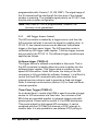
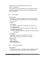
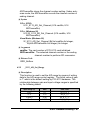
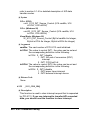
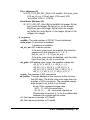
The outstanding features of PCI-9113 is that isolated
programmable amplifier is used between analog input lines and
A/D converter. It can protect all of the A/D converters, your PC,
and peripherals from damage due to the high voltages on the
analog inputs. The block diagram of PCI-9113 is shown below.
DC/DC
CONVERTER
Isolation
+15
CH 0
CH 1
CH 2
32
.
.
.
CH 31
ISO
AMP
12 Bit
A/D Converter
(ADS774)
Single-ended
Analog
Multiplexer
CONTROL
LOGIC
1K A/D FIFO
(Analog Input)
Bootstrape
EPROM
PCI Bus
Controller
Local Bus
32-bit PCI Local Bus
Introduction •1
1.1
Software Supporting
There are several software options to help you to implement your
applications quickly and easily.
Custom Program
For the customers writing their own programs, the PCI-9113 is
supported by a comprehensive set of drivers and programming
tools. These software drivers support multiple platforms.
• MS-DOS Borland C++ programming library.
• Dynamic linking library (DLL) for Win-95.
• PCIS-DASK/NT : Advanced data acquisition software kit for
Windows NT.
The MS-DOS Borland C++ library and DLL for Win-95 are
included in ADLink’s “Manual & Software Utility”CD in this
package.
1.2
Features
The PCI-9113 PCI Bus Advanced Data Acquisition Card provides
the following advanced features:
• 32-bit PCI-Bus, Plug and Play
• 32-CH 12-bit single-ended analog inputs
• Isolation 1500Vrms continuous, 2500Vrms for one minute
• Programmable gain of 1, 10, 100
• Sampling rate up to 60KHz
• Trigger mode: software trigger, timer pacer, external trigger
• On-board A/D 1K WORDS FIFO memory
• Auto-scanning channel selection
2 •Introduction
• DB-37 connector, pin assignment is compatible with ACL8113
• Input impedance: 10M Ω
• Voltage protection: 70 voltage (peak-to-peak)
1.3
Applications
• Industrial process control
• Transducer, thermocouple, RTD
• Power monitor
• Medical instrument
• Biomedical measurement
• Ground loop elimination
1.4
Specifications
♦ Analog Input (A/D)
• Converter : B.B. ADS774, successive approximation type
• Resolution : 12-bit
• Input channels : 32 single-ended
• Isolated programmable gain amplifier
Isolation voltage rated continuous:
1,500Vrms, 2,500Vrms for one minute
Isolation-Mode Rejection: 115dB
Barrier Impedance: 10MΩ ll 10 pf
Leakage Current: 0.8 µ Ams
• Input Range : (Software controlled, and jumper selection)
Bipolar : ±10V, ±1V , ±0.1V or ±5V, ±0.5V, ±0.05V
Introduction •3
Unipolar : 0~10V, 0~1V, 0~0.1V
4 •Introduction
• Throughput:
Gain = 1
60K
Gain = 10
60K
Gain = 100
10K
• Overvoltage Protection: Continuous ±35V maximum
• Accuracy: 0.015% of reading ±1 bit
• Input Impedance: 10 MΩ
• Trigger Mode: Software and Pacer
• Data Transfer: Program control, Interrupt
• FIFO Buffer Size: 1024 samples
♦
General Specifications
• Connector : 37-pin D-type connector
• Operating Temperature : 0°C ~ 55°C
• Storage Temperature : -20°C ~ 80°C
• Humidity : 5 ~ 95%, non-condensing
• Power Consumption : +5 V @ 960mA (max.)
• Dimension : 6.77” (172mm) (L) x 4.13” (105mm) (W)
Introduction •5
2
Installation
This chapter describes how to install the PCI-9113. At first, the
contents in the package and unpacking information that you
should be careful are described.
2.1
What You Have
In addition to this User's Manual, the package includes the
following items:
• PCI-9113 Enhanced Multi-function Data Acquisition Card
• Manual & Software Utility CD
If any of these items is missing or damaged, contact the dealer
from whom you purchased the product. Save the shipping
materials and carton in case you want to ship or store the product
in the future.
Installation •7
2.2
Unpacking
Your PCI-9113 card contains sensitive electronic components that
can be easily damaged by static electricity.
The card should be done on a grounded anti-static mat. The
operator should be wearing an anti-static wristband, grounded at
the same point as the anti-static mat.
Inspect the card module carton for obvious damage. Shipping and
handling may cause damage to your module. Be sure there are
no shipping and handing damages on the module before
processing.
After opening the card module carton, extract the system module
and place it only on a grounded anti-static surface component
side up.
Again inspect the module for damage. Press down on all the
socketed IC's to make sure that they are properly seated. Do this
only with the module place on a firm flat surface.
Note: DO NOT APPLY POWER TO THE CARD IF IT HAS
BEEN DAMAGED.
You are now ready to install your PCI-9113.
2.3
Device Installation for Windows 95
While you first plug PCI-9113 card and enter Windows 95, the
system will detect this device automatically and show the
following dialog box that prompts you to select the device
information source.
8 •Installation
Choose the default option “Driver from disk provided by hardware
manufacturer”and then a dialog box is shown to prompt you give
the path of installation disk.
Place ADLink’s “Manual & Software Utility”CD into the
appropriate CD driver. Type “X:\Software\Pci_Card\9113\Win95”
(this directory includes PCI-9113 device information file
“9113.inf”) in the input field (X indicates the CD ROM driver)
Installation •9
and then click OK. The system will start the installation of PCI9113.
10 •Installation
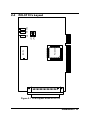
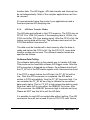
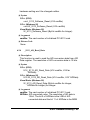
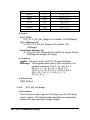
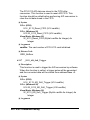
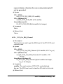
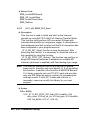
PCI-9050
JP2
JP1
VR1 VR2 VR3
PCI-9113's Layout
ISO174
2.4
Figure 2.1 PCB Layout of the PCI-9113
Installation •11
2.5
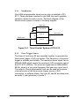
Jumper Descriptions
2.5.1
Polarity Selection Jumper
JP1 is the polarity selection jumper. The following diagram shows
the possible configurations.
Bi-polar input
Uni-polar input
2.5.2
Full Range Jumper
JP2 set the full range of the analog input channels. The following
diagram shows the possible configurations.
20V Full Range
10V Full Range
2.5.3
Possible AD Input Range Configurations
The JP1 and JP2 are used to setup the analog input signal range.
There are three possible combinations, 0~10V, -5V~+5V and –
10V ~ +10V. See the following table for reference.
JP2
JP1
12 •Installation
1-2
2-3
2-3
+/-5V
0~10V
1-2
+/-10V
X
2.6
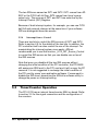
PCI Configuration
1. Plug and Play :
As a plug and play component, the board requests an interrupt via
a system call. The system BIOS assigns an interrupt level based
on the board information and system parameters. These system
parameters are determined by the installed drivers and the
hardware load seen by the system.
2. Configuration :
The board configuration is done on a board-by-board basis for all
PCI cards on your system. Because the configuration is controlled
by the system BIOS and software, there is no jumpers for setting
system parameters like base-address, and interrupt level.
The configuration is subject to change with every boot of the
system when new boards are added or boards are removed.
3. Trouble shooting :
If your system will not boot or if you experience erratic operation
with your PCI board in place, it’s likely caused by an interrupt
conflict (perhaps because you incorrectly described the ISA
setup). In general, the solution, once you determine it is not a
simple oversight, is to consult the BIOS documentation that come
with your system.
Installation •13
3
Signal Connections
This chapter describes the connector of PCI-9113, and the signal
connection between the PCI-9113 and external devices, such as
daughter boards or other devices.
3.1
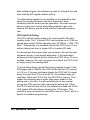
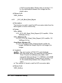
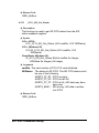
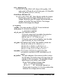
Connectors Pin Assignment
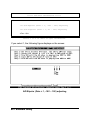
The PCI-9113 comes equipped one 37-pin D-type connector CN1. The pin assignment of CN1 is illustrated in the Figure 3.1.
Signal Connections •15
•CN 1 : Analog Input Signals
CN1
AI0
AI2
AI4
AI6
AI8
AI10
AI12
AI14
IGND
IGND
AI16
AI18
AI20
AI22
AI24
AI26
AI28
AI30
IGND
1
2
3
4
5
6
7
8
9
10
11
12
13
14
15
16
17
18
19
20
21
22
23
24
25
26
27
28
29
30
31
32
33
34
35
36
37
AI1
AI3
AI5
AI7
AI9
AI11
AI13
AI15
IGND
IGND
AI17
AI19
AI21
AI23
AI25
AI27
AI29
AI31
Figure 3.1 Pin Assignment of CN1
Legend :
AIn
IGND
3.2
: Analog Input Channel n (single-ended)
: lsolated Signal Ground
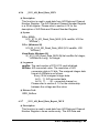
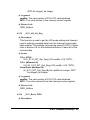
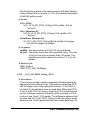
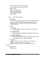
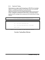
Analog Input Signal Connection
The PCI-9113 provides 32 single-ended analog input signals
which can be converted to digital value by the A/D converter. To
avoid ground loops and get more accurate measurement of A/D
conversion, it is quite important to understand the signal source
type. The single-ended mode has only one input relative to
ground and is suitable for connecting with the floating signal
source. The floating source means it does not have any
connection to real ground. Figure 3.2 shows the single-ended
connection. Note that when more than two floating sources are
connected, the sources must be with common ground.
16 •Signal Connections
AIn
Floating
Signal
Source
Input Multipexer
Opertional
Amplifier
...
V1
To A/D Converter
V2
n = 0, ...,31
IGND
Figure 3.2 Floating sources and single-ended connection
3.3
Daughter Board Connection
The PCI-9113 can be connected with several different daughter
boards, ACLD-9881, ACLD-9137 and ACLD-9188. The
functionality and connections are specified as follows.
3.3.1
Connect with ACLD-9881
The ACLD-9881 has a 37-pin D-sub connector, which can connect
with PCI-9113 through 37-pin assemble cable. The ACLD-9881
provides low pass filter for the 32 channels, it is very flexible for
wiring.
3.3.2
Connect with ACLD-9137
The ACLD-9137 is a direct connector for the card which is
equipped with 37-pin D-sub connector. This board provides a
simple way for connection. It is very suitable for the simple
applications that do not need complex signal condition before the
A/D conversion is performed.
3.3.3
Connect with ACLD-9188
ACLD-9188 is general purpose terminal boards for all the card
which comes equipped with 37-pin D-sub connector.
Signal Connections •17
4
Registers Structure & Format
The detailed descriptions of the register format of the PCI-9113
are specified in this chapter. This information is quite useful for
the programmers who wish to handle the card by low-level
programming. In addition, users can understand how to use
software driver to manipulate this card after understanding the
registers' structure of the PCI-9113.
4.1
I/O Port Address
The PCI-9113 functions as a 32-bit PCI target device to any
master on the PCI bus. There are three types of registers on the
PCI-9113: PCI Configuration Registers (PCR), Local
Configuration Registers (LCR) and PCI-9113 registers.
The PCR which conforms the PCI-bus specifications are
initialized and controlled by the system plug & play PCI BIOS.
Users can study the PCI BIOS specifications to understand the
operation of the PCR. The PCR can only be read through by PCI
BIOS function call.
The LCR are specified by the PCI bus controller PLX-9050. It is
not necessary for users to understand the details of the LCR if
Registers Structure & Format •19
you use the software library. The base address of the LCR is
assigned by the PCI p&p BIOS. The assigned address is located
at offset 14h of PCR.
The PCI-9113 registers are shown in the Table 4.1. The base
address of the PCI-9113 registers is also assigned by the PCI p&p
BIOS. The assigned base address is located at offset 18h of PCR.
Note that most of the PCI-9113 registers are 16 bits. The users
can access these registers by 16 bits I/O instructions.
There is one 32 bits register on PCI-9113. The 32 bits register
occupied another LCR address space, that is, base address #2.
The base address is allocated by PCI BIOS and is stored at offset
1Ch of PCR.
Users can read the PCR to get the LCR base address and the two
PCI-9113 base addresses by using the PCI BIOS function call.
I/O Base Address #1
Write
Read
Base + 00h
Base + 02h
Base + 04h
Base + 06h
Base + 08h
Base + 0Ah
I/O Base Address #2
AD MUX channel no.
AD range control
AD trigger mode
Interrupt control
Software AD trigger
Clear H/W IRQ
Write
AD FIFO value
AD status read back
AD trigger mode
Interrupt setting Read Back
--Read
Base 2 + 00h
--
AD data and channel
number
Table 4.1 I/O Address
4.2
A/D Data Registers
The PCI-9113 A/D data is stored in the FIFO after conversion.
The data can be transferred to host memory by software only.
The register is 12 bits and can be read by 16 bits I/O command.
20 •Registers Structure & Format
Address : BASE + 0
Attribute : read only
Data Format :
Bit
7
6
5
4
3
2
1
0
BASE+0
BASE+1
AD7
x
AD6
x
AD5
x
AD4
x
AD3
AD11
AD2
AD10
AD1
AD9
AD0
AD8
AD11 .. AD0 : Analog to digital data. AD11 is the Most Significant
Bit (MSB) of PCI-9113. AD0 is the Least Significant
Bit(LSB).
4.3
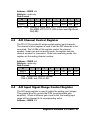
A/D Channel Control Register
The PCI-9113 provides 32 single-ended analog input channels.
The channel control register is used to set the A/D channels to be
converted. The 5 LSBs of this register control the channel
number. Under non-auto scanning mode, the register sets the
channel number for conversion. Under auto-scanning mode, the
register set the ending channel number.
Address : BASE + 0
Attribute : write only
Data Format :
Bit
7
6
5
4
3
2
1
0
BASE+0
BASE+1
x
x
x
x
x
x
CN4
x
CN3
x
CN2
x
CN1
x
CN0
x
CNn : multiplexer channel number.
CN4 is MSB, and CN0 is LSB.
4.4
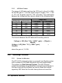
A/D Input Signal Range Control Register
The A/D range register is used to adjust the analog input ranges.
This register directly controls the PGA (programmable gain
amplifier). When a different gain value is set, the analog input
range will be changed to its corresponding value.
Address : BASE + 2
Registers Structure & Format •21
Attribute : write only
Data Format :
Bit
BASE+2
BASE+3
7
X
X
6
X
X
5
X
X
4
X
X
3
X
X
2
X
X
1
G1
X
0
G0
X
GC0~GC1: A/D Range control setting
The relationship between gain setting and its corresponding A/D
range is listed in the table below.
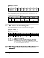
4.5
G2
G1
GAIN
0
0
1
0
1
1
0
10
100
Analog Input Range
Bi-Polar
Uni-Polar
10 V
±10V
±5V
±1V
±100mV
±500mV
±50mV
1V
100mV
A/D Status Readback Register
The A/D FIFO status can be read back from this register.
Address : BASE + 2
Attribute : read only
Data Format :
Bit
BASE+2
BASE+3
7
X
X
6
X
X
5
X
X
4
X
X
3
AD_BUSY
X
2
FF_FF
X
1
FF_HF
X
0
FF_EF
X
FF_EF : ‘0’means FIFO is empty
FF_HF : ‘0’means FIFO is half-full
FF_FF : ‘0’means FIFO is full, A/D data may have been loss
AD_BUSY : ‘0’means AD is busy, the A/D data has not been
latched in FIFO yet. If AD_BUSY changes from ‘0’to
‘1’, A/D data is written into FIFO.
4.6
A/D Trigger Mode Control and Readback
Register
22 •Registers Structure & Format
This register is used to control or read back the A/D trigger control
setting and the A/D range setting.
Address : BASE + 4
Attribute : write and read
Data Format :
Bit
BASE+4
BASE+5
7
X
X
6
X
X
5
X
X
4
X
X
3
G1
X
2
G0
X
1
TSSEL
X
0
ASCAN
X
GC0~GC1: A/D range setting, read back (only)
TSSEL : Timer Pacer / Software Trigger
1: Timer Pacer Trigger
0: Software Trigger
ASCAN: Auto Scan Control
1: Auto Scan ON
0: Auto Scan OFF
4.7
Software Trigger Register
To generate a trigger pulse to the PCI-9113 for A/D conversion,
you just write any data to this register, then the A/D converter will
be triggered.
Address : BASE + 8
Attribute : write only
Data Format :
Bit
BASE+8
4.8
7
X
6
X
5
X
4
X
3
X
2
X
1
X
0
X
Interrupt Control and Readback Register
The PCI-9113 has a dual interrupt system, thus two interrupt
sources can be generated and be checked by the software. This
register is used to select the interrupt sources.
Address : BASE + 6
Registers Structure & Format •23
Attribute : write and read
Data Format :
Bit
BASE+12
7
X
6
X
5
X
4
X
3
X
2
FFEN
1
ISC1
0
ISC0
ISC0 : IRQ0 signal select
0 : IRQ on the ending of the AD conversion (EOC)
1 : IRQ when FIFO is half full
ISC1 : IRQ1 signal select (Timer Interrupt only)
FFEN : FIFO enable pin
0: FIFO Enable (Power On Default value)
1: FIFO Disable
(To reset FIFO, set FFEN sequence as 0 -> 1 -> 0)
4.9
Hardware Interrupt Clear Register
Because the PCI interrupt signal is level trigger, the interrupt clear
register must be written to clear the flag after processing the
interrupt request event; otherwise, that another interrupt request is
inserted will cause the software to hang on processing the
interrupt event.
Address : BASE + 0Ah
Attribute : write only
Data Format :
Bit
BASE+0Ah
7
X
6
X
5
X
4
X
3
X
2
X
1
X
0
X
4.10 A/D Data and Channel Number Registers
The PCI-9113 A/D data and channel number is stored in the
FIFO. Reading this register by a 32-bit I/O instruction can read
back the data and channel number simultaneously.
Address : BASE 2 + 0
Attribute : read only
Data Format :
24 •Registers Structure & Format
Bit
7
6
5
4
3
2
1
0
BASE2+0
BASE2+1
BASE2+2
BASE2+3
AD7
x
x
x
AD6
X
X
X
AD5
x
x
x
AD4
x
CN4
x
AD3
AD11
CN3
x
AD2
AD10
CN2
x
AD1
AD9
CN1
x
AD0
AD8
CN0
x
AD11~AD0 : Analog to digital data. AD11 is the Most Significant
Bit (MSB) of PCI-9113. AD0 is the Least Significant
Bit (LSB).
CN4~CN0 : Channel number
4.11 High Level Programming
To operate the PCI-9113, you can bypass the detailed register
structures and use the high-level application programming
interface (API) to control your PCI-9113 card directly. The
software libraries, DOS library for Borland C++, and DLL for
Windows 95 are included in the ADLink’s “Manual & Software
Utility”CD. Please refer to chapter 6 for more detailed
information.
4.12 Low-Level Programming
To operate the PCI-9113, users do not need to understand how to
write a hardware dependent low-level program. The control of the
PCI controller is complex and not described in the manual. It is
not recommended the user to program applications based on lowlevel programming. If the user does need to program in low-level
programming, you can contact the dealer from whom you
purchased the PCI-9113 for further PCI controller programming
information.
Registers Structure & Format •25
5
Operation Theorem
The operation theorem of the functions on PCI-9113 card is
described in this chapter. The operation theorem can help you to
understand how to manipulate or to program the PCI-9113.
5.1
A/D Conversion
Before programming the PCI-9113 to perform the A/D conversion,
you should understand the following issues:
• A/D conversion procedure
• A/D signal source control
• A/D trigger source control
• A/D data transfer mode
• Interrupt System (refer to section 5.2)
• A/D data format
Note : Because some of the A/D data transfer modes will use the
system interrupt resource, the users have to understand the
interrupt system (section 5.2) in the same time.
Operation Theorem •27
5.1.1
A/D Conversion Procedure
For using the A/D converter, users must know about the property
of the signal to be measured at first. The users can decide which
channels to be used and connect the signals to the PCI-9113.
Refer to the chapter 3 ‘Signal Connection’. In addition, users
should define and control the A/D signal sources, including the
A/D channel, A/D gain, and A/D signal types. Please refer to
section 5.1.2. for A/D signal source control.
After deciding the A/D signal source, the user must decide how to
trigger the A/D conversion and define/control the trigger source.
The A/D converter will start to convert the signal to a digital value
when a trigger signal is rising. Refer to the section 5.1.3 for the
two trigger sources.
The A/D data should be transferred into PC's memory for further
using or processing. The data can be read by I/O instruction which
is handled directly by software or transferred to memory via
interrupt. Please refer to section 5.1.4 to obtain ideas about the
multi-configurations for A/D data transfer.
To process A/D data, programmer should know about the A/D
data format. Refer to section 5.1.5 for details.
5.1.2
A/D Signal Source Control
To control the A/D signal source, the signal type, signal channel
and signal range should be considered.
Signal Type & Signal Conditioning
The A/D signal sources of PCI-9113 could be single ended (SE)
only. Three are 32 SE A/D channels on board. The R/C filters
(attenuantors) are on board for every channel. The RC circuits for
each channel is shown in the following diagram, where ‘n’is the
channel number. User can install the R, C for special purpose
such as attenuating the voltage to increase the input voltage
range.
28 •Operation Theorem
Analog Input
Channel #n
RAn
0. Ohm
RBn
OPEN
To Multiplexer
CAn
OPEN
The RC network can also be used as current sensor, which
transfers the current into voltage. To get the ground reference
level, user can cut-off RA and let RB = 0 Ohm, thus grounding the
input signal. The users can use the ground input to calibrate the
offset voltage by software.
Signal Channel Control
There are two ways to control the channel number. The first one
is the software programming and the second one is the auto
channel scanning which is controlled by the ASCAN bit in AD
trigger mode control register. As ASCAN is cleared (0), the value
of AD channel Control register defines the channel to be selected.
As ASCAN is set 1, the value in AD channel control register
defines the ending channel number of auto-scanning operation.
Under auto scan mode, the channel is scanning from channel 0 to
the ending channel. Whenever a trigger signal is rising, the
channel number to be selected will increase automatically. For
example, if the ending channel number is 3, the auto channel
scanning sequence is 0,1,2,3,0,1,2,3, … , until the ASCAN bit is
cleared.
Signal Range
The proper signal range is important for data acquisition. The
input signal may be saturated if the A/D gain is too large.
Sometimes, the resolution may be not enough if the signal is
small. The maximum A/D signal range of PCI-9113 is ±10 volts
when the A/D gain value is 1. The A/D gain control register
controls the maximum signal input range. The signal gain is
Operation Theorem •29
programmable with 4 levels (1,10,100,1000*). The signal range of
the 32 channels will be identical all the time even if the channel
number is scanning. The available signal polarity on PCI-9113 are
bi-polar and uni-polar configuration.
*Note: Gain value of 1000 is programmable, however, the
accuracy is not guaranteed.
5.1.3
A/D Trigger Source Control
The A/D conversion is started by a trigger source, and then the
A/D converter will start to convert the signal to a digital value. In
PCI-9113, two internal sources can be selected: the software
trigger or the timer pacer trigger. The A/D operation mode is
controlled by A/D trigger mode register. Total two trigger sources
are provided in the PCI-9113. The different trigger conditions are
specified as follows:
Software trigger (TSSEL=0)
The trigger source is software controllable in this mode. That is,
the A/D conversion is starting when any value is written into the
software trigger register. This trigger mode is suitable for low
speed A/D conversion. Under this mode, the timing of the A/D
conversion is fully controlled by software. However, it is difficult to
control the fixed A/D conversion rate unless another timer
interrupt service routine is used to generate a fixed rate trigger.
Refer to interrupt control section (section 5.2) for fixed rate timer
interrupt operation.
Timer Pacer Trigger (TSSEL=1)
An on-board timer / counter chip 8254 is used to provide a trigger
source for A/D conversion at a fixed rate. Two counters of the
8254 chip are cascaded together to generate trigger pulse with
precise period. Please refer to section 5.3 for 8254 architecture.
This mode is ideal for high speed A/D conversion. It can be
combined with the FIFO half-full interrupt or EOC interrupt to
transfer data. It is also possible to use software FIFO polling to
30 •Operation Theorem
transfer data. The A/D trigger, A/D data transfer and Interrupt can
be set independently. Most of the complex applications can thus
be covered.
It's recommended using this mode if your applications need a
fixed and precise A/D sampling rate.
5.1.4
A/D Data Transfer Modes
The A/D data are buffered in the FIFO memory. The FIFO size on
PCI-9113 is 1024 (1K) words. If the sampling rate is 10 KHz, the
FIFO can buffer 102.4 ms analog signal. After the FIFO is full, the
lasting coming data will be lost. The software must read out the
FIFO data before it becomes full.
The data must be transferred to host memory after the date is
ready and before the FIFO is full. On the PCI-9113, many data
transfer modes can be used. The different transfer modes are
specified as follows:
Software Data Polling
The software data polling is the easiest way to transfer A/D data.
This mode can be used with software A/D trigger mode. After the
A/D conversion is triggered by software, the software should poll
the FF_EF bit of the A/D status register until it becomes low level.
If the FIFO is empty before the A/D start, the FF_EF bit will be
low. After the A/D conversion is completed, the A/D data is
written to FIFO immediately, thus the FF_EF becomes high. You
can consider the FF_EF bit as a flag to indicate the converted
data ready status. That is, FF_EF is high means the data is ready.
Note that, while A/D is converted, the ADBUSY bit is low. After
A/D conversion, the ADBUSY becomes high to indicate not busy.
Please do NOT use this bit to poll the AD data.
It is possible to read A/D converted data without polling. The A/D
conversion time will not exceed 8.5µs on PCI-9113 card. Hence,
Operation Theorem •31
after software trigger, the software can wait for at least 8.5µs and
then read the A/D register without polling.
The data polling transfer is very suitable for the application that
needs to process AD data in real time. Especially, when
combining with the timer interrupt generation, the timer interrupt
service routine can use the data polling method to get multichannel A/D data in real time and with the fixed data sampling
rate.
FIFO Half-Full Polling
The FIFO half-full polling mode is the most powerful AD data
transfer mode. The 1 K words FIFO can be stored up to 10.24 ms
analog data under 100 KHz sampling rate (10.024ms = 1024 / 100
KHz ). Theoretically, the software can poll the FIFO every 10 ms
without taking care how to trigger A/D or transfer A/D data.
It’s recommend that users check your system to find out the user
software‘s priority in the special application. If the application
software is at the highest priority, polling the FIFO every 10 ms is
suitable. However, the user‘s program must check the FIFO is full
or empty every time reading data.
To avoid this problem, the half-full polling method is used. If the
A/D trigger rate is 100KHz, the FIFO will be half-full (512 words)
in 5.12 ms. If the user‘s software checks the FIFO half full signal
every 5 ms and the FIFO is not half-full, the software does not
read data. When the FIFO is full, the AD FIFO is overrun. That
means the sampling rate is higher than users’expect or the
polling rate is too slow. It is also possible due to your system
occupy the CPU resource thus reducing the polling rate. When
the FIFO is half-full and not full, the software can read one “block”
(512 words) A/D data without checking the FIFO status. This
method is very convenient to read A/D in size of a “block”and it is
benefit to software programming.
32 •Operation Theorem
Usually, the timer trigger is used under this mode, therefore the
sampling rate is fixed. The method also utilizes the minimum
CPU resources because it is not necessary to be the highest
priority. The other benefit is this method will not use hardware
interrupt resource. Therefore, the interrupt is reserved for system
clock or emergency external interrupt request. The FIFO half-full
polling method is the most powerful A/D data transfer mode.
EOC Interrupt Transfer
The PCI-9113 provides traditional hardware end-of-conversion
(EOC) interrupt capability. Under this mode, an interrupt signal is
generated when the A/D conversion is ended and the data is
ready to be read in the FIFO. It is useful to combine the EOC
interrupt transfer with the timer pacer trigger mode. After A/D
conversion is completed, the hardware interrupt will be inserted
and its corresponding ISR (Interrupt Service Routine) will be
invoked and executed. The ISR program can read the converted
data. This method is most suitable for data processing
applications under real-time and fixed sampling rate
FIFO Half-Full Interrupt Transfer
Sometimes, the applications do not need real-time processing,
but the foreground program is too busy to poll the FIFO data. The
FIFO half-full interrupt transfer mode is useful for the situation
mentioned above. In addition, as the external A/D trigger source
is used, the sampling rate may be not easy to predict, and then
the method could be applied. Because the CPU is only interrupted
when the FIFO is half-full, thus reserved the CPU load.
Under this mode, an interrupt signal is generated when FIFO
becomes half-full. It means there are 512 words data in the FIFO
already. The ISR can read a block of data every interrupt
occurring. This method is very convenient to read A/D in size of a
“block”(512 words) and it is benefit for software programming.
Operation Theorem •33
5.1.5
A/D Data Format
The range of A/D data read from the FIFO port is from 0 to 4095.
As the A/D gain is 1, the A/D signal range is roughly -10V ~ +10V
or -5V~+5V (bi-polar) and 0V~+10V (uni-polar). The relationship
between the voltage and the value is shown in the following table:
A/D Data (Hex)
Decimal Value
FFF
C00
801
800
7FF
400
000
4095
3072
2049
2048
2047
1024
0
Voltage (Volts)
±10V (Bipoar)
0~10V(Unipoar)
+9.9951
+9.9951
+5.0000
+7.5000
+0.0049
+5.0049
0.0000
+5.0000
-0.0049
+4.9951
-5.0000
+2.5000
-0.0000
0.0000
The formula between the A/D data and the analog value is
Voltage = ( AD_Data * 20 ) / ( 4096 * gain ) – (10/gain) -Bipolar
Voltage = ( AD_Data * 10 ) / ( 4096 * gain )
-Unipolar
where the gain is 1,10,100.
5.2
Interrupt Control
5.2.1
System Architecture
The PCI-9113‘s interrupt system is a powerful and flexible system
that is suitable for A/D data acquisition and many applications.
The system is a Dual Interrupt System. The dual interrupt
means the hardware can generate two interrupt request signals in
the same time and the software can service these two request
signals by ISR. Note that the dual interrupt does not mean the
34 •Operation Theorem
card occupies two IRQ levels.
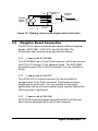
The two interrupt request signals (INT1 and INT2) come from
digital signals or the timer / counter output. An interrupt source
multiplexer (MUX) is used to select the IRQ sources. Fig 5.2.1
shows the interrupt system.
INT #A
PCI
Controller
INT1
INT2
IRQ
FlipFlops
AD EOC
FIFO
Half-full
INT1
MUX
Timer Pacer
Clear IRQ
Fig 5.2.1 Dual Interrupt System of PCI-9113
5.2.2
IRQ Level Setting
There is only one IRQ level used by this card, although it is a dual
interrupt system. This card uses INT #A interrupt request signal to
PCI bus. The motherboard circuits will transfer INT #A to one of
the AT bus IRQ levels. The IRQ level is set by the PCI plug and
play BIOS and saved in the PCI controller. It is not necessary for
users to set the IRQ level.
5.2.3
Dual Interrupt System
The PCI controller of PCI-9113 can receive two hardware IRQ
sources. However, a PCI controller can generate only one IRQ to
PCI bus, the two IRQ sources should be distinguished by ISR of
the application software if the two IRQ are all used.
The application software can use the “_9113_Get_Irq_Status”
function to distinguish which interrupt is inserted. After servicing
an IRQ signal, users should check if another IRQ is also asserted
and then clear current IRQ to allow the next IRQ occurring.
Operation Theorem •35
The two IRQs are named as INT1 and INT2. INT1 comes from AD
EOC or the FIFO half-full flag. INT2 comes from timer‘s pacer
output only. The sources of INT1 and INT2 are selective by the
Interrupt Control (ISC) Register.
Because of dual interrupt system, for example, you can use FIFO
half-full and external interrupt at the same time if your software
ISR can distinguish these two events.
5.2.4
Interrupt Source Control
There are two bits to control the IRQ sources of INT1 and INT2.
Refer to section 4.9 for the details of the two bits. In addition, the
PCI controller itself can also control the use of the interrupt. For
manipulating the interrupt system more easily, ADLink
recommends you to use the function _9113_INT_Source_Control
to control the IRQ source so that you can disable one or two of
the IRQ sources.
Note that even you disable all the two IRQ sources without
changing the initial condition of the PCI controller, the PCI BIOS
still assigns an IRQ level to the PCI card and it will occupy the PC
resource. It is not suggested to re-design the initial condition of
the PCI card by users‘own application software. If users want to
disable the IRQ level, please use the ADLink’s software utility to
change the power on interrupt setting.
5.3
Timer/Counter Operation
The PCI-9113 has an interval timer/counter 8254 on board. Refer
to section 3.5 for the signal connection and the configuration of
the counters.
36 •Operation Theorem
5.3.1
Introduction
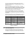
One 8254 programmable timer/counter chip is installed in PCI9113. There are three counters in one 8254 chip and 6 possible
operation modes for each counter. The block diagram of the
timer/counter system is shown in following diagram.
8254 Chip
C
Counter #0
O
Timer #1
O
Timer #2
O
G
C
Timer Pacer
'H' G
2 MHz Clock
C
'H' G
Figure 5.3.1 Timer/Counter System of PCI-9113.
5.3.2
Pacer Trigger Source
The timer #1 and timer #2 are cascaded together to generate the
timer pacer trigger of A/D conversion. The frequency of the pacer
trigger is software controllable. The maximum pacer signal rate is
2MHz/4=500K which excess the maximum A/D conversion rate of
the PCI-9113 (80KHz). The minimum signal rate is 2MHz/65535/
65535, which is a very slow frequency that user may never use it.
The output of the programmable timer can be used as the pacer
interrupt source or the timer pacer trigger source of A/D
conversion. In software library, the timer #1 and #2 are always set
as mode 2 (rate generator) or mode 3.
Operation Theorem •37
6
C/C++ Software Library
There are 36 functions provided by the C Language library. This
library includes all the functions of PCI-9113. The major capability
of these function calls is A/D conversion. In addition, there are
some sample programs to help you to use this library.
6.1
Installation
6.1.1
Installation
u MS-DOS Software Installation
step 1. Place ADLink’s “Manual & Software Utility”CD
into the appropriate CD drive.
step 2. Type the command (X indicates the CD ROM
driver):
X:\> CD Software\Pci_Card\9113\DOS
X:\ Software\Pci_Card\9113\DOS> SETUP
step 3. An installation complete message will be shown
on the screen.
After installation, all the files of PCI-9113 Library & Utility
for DOS are stored in C:\ADLink\9113\DOS directory.
C/C++ Software Library •39
u Windows 95 Software Installation
step 1. Place ADLink’s “Manual & Software Utility”CD
into the appropriate CD driver.
step 2. If Windows 95 is loaded, choose Run from the
Start menu.
step 3. Type X:\Software\Pci_Card\9113\Win95\Setup.exe
in the Run dialog box. (X indicates the CD ROM
driver).
After a welcome dialog box, Setup prompts the following
dialog box for you to specify the destination directory. The
default path is C:\9113w95. If you want to install PCI-9113
DLL for Windows 95 in another directory, please click
Browse button to change the destination directory.
Then you can click Next to begin installing PCI-9113 DLL
for Windows 95.
Then you can click Next to begin installing PCI-9113 DLL
for Windows 95.
40 •C/C++ Software Library
After you complete the installation of PCI-9113 Software,
PCI-9113’s DLL (9113.DLL) is copied to Windows System
directory (default is C:\WINDOWS\SYSTEM) and the
driver files (W95_9113.VXD and PCIW95.VXD) are also
copied to the appropriate directory.
6.2
C/C++ Programming Library
We defined some data types in acl_pci.h. These data types are
used by PCI-9113 library. We suggest you to use these data types
in your application programs. The following table shows the data
type names and their range.
6.2.1
Data Types
Type Name
U8
I16
U16
I32
U32
F32
F64
Boolean
Description
8-bit ASCII character
16-bit signed integer
16-bit unsigned integer
32-bit signed integer
32-bit single-precision floating-point
32-bit single-precision floating-point
64-bit double-precision floating-point
Boolean logic value
Range
0 to 255
-32768 to 32767
0 to 65535
-2147483648 to 2147483647
0 to 4294967295
-3.402823E38 to 3.402823E38
-1.797683134862315E308 to
1.797683134862315E309
TRUE, FALSE
The functions of PCI-9113's software drivers use full-names to
represent the functions' real meaning. The naming convention
rules are :
In DOS Environment :
_{hardware_model}_{action_name}. e.g. _9113_Initial().
In order to recognize the difference between DOS library and
Windows 95 library, A capital "W" is put on the head of each
C/C++ Software Library •41
function name of the Windows 95 DLL driver. e.g.
W_9113_Initial().
There are 36 functions provided by PCI-9113 software drivers.
The detail descriptions of each function are specified in the
following sections.
6.2.2
_9113_Initial
@ Description
This function is used to initialize PCI-9113 card. Every PCI9113 card has to be initialized by this function before calling
other functions.
@ Syntax
C/C++ (DOS)
U16 _9113_Initial (U16 *existCards, PCI_INFO *info)
C/C++ (Windows 95)
U16 W_9113_Initial (U16 *existCards, PCI_INFO *info)
Visual Basic (Windows 95)
W_9113_Initial (existCards As Integer, info As PCI_INFO)
As Integer
@ Argument
existCards: numbers of existing PCI-9113 cards
info: relative information of the PCI-9113 cards
@ Return Code
ERR_NoError
ERR_BoardNoInit
ERR_PCIBiosNotExist
6.2.3
_9113_Software_Reset
@ Description
This function is used to reset the I/O port configuration. Note
that this function can not re-start the PCI bus and all the
42 •C/C++ Software Library
hardware setting won’t be changed neither.
@ Syntax
C/C++ (DOS)
void _9113_Software_Reset (U16 cardNo)
C/C++ (Windows 95)
void W_9113_Software_Reset (U16 cardNo)
Visual Basic (Windows 95)
W_9113_Software_Reset (ByVal cardNo As Integer)
@ Argument
cardNo: The card number of initialized PCI-9113 card
@ Return Code
None
6.2.4
_9113_AD_Read_Data
@ Description
This function is used to read the A/D conversion data from A/D
Data register. The resolution of A/D conversion data is 12 bits.
@ Syntax
C/C++ (DOS)
U16 _9113_AD_Read_Data (U16 cardNo, U16 far
*ADData)
C/C++ (Windows 95)
U16 W_9113_AD_Read_Data (U16 cardNo, U16 *ADData)
Visual Basic (Windows 95)
W_9113_AD_Read_Data (ByVal cardNo As Integer,
ADData As Integer) As Integer
@ Argument
cardNo: The card number of initialized PCI-9113 card.
ADData: A/D converted value. The resolution of AD data is
12-bit. The bit 0 of ADData is the LSB of A/D
converted data and the bit 11 of ADData is the MSB
C/C++ Software Library •43
of A/D converted data. Please refer to section 5.1.5
for the relationship between the voltage and the
digital value.
@ Return Code
ERR_NoError
6.2.5
_9113_AD_Read_Data_Repeat
@ Description
This function is used to read the A/D conversion data from the
data register n times continuously.
@ Syntax
C/C++ (DOS)
U16 _9113_AD_Read_Data_Repeat (U16 cardNo, I16 far
*ADData, U16 n)
C/C++ (Windows 95)
U16 W_9113_AD_Read_Data_Repeat (U16 cardNo, I16
*ADData, U16 n)
Visual Basic (Windows 95)
W_9113_AD_Read_Data_Repeat (ByVal cardNo As
Integer, ADData As Integer, ByVal n As Integer) As
Integer
@ Argument
cardNo: The card number of PCI-9113 card initialized
ADData: A/D converted value. The resolution of A/D data is
12-bit. The bit 0 of ADData is the LSB of A/D
converted data and the bit 11 of ADData is the MSB
of A/D converted data. Please refer to section 5.1.5
for the relationship between the voltage and the
value.
n: The number of times to read the A/D conversion data.
@ Return Code
ERR_NoError
44 •C/C++ Software Library
6.2.6
_9113_AD_Read_Data_MUX
@ Description
This function is used to read data from A/D Data and Channel
Number Register. The A/D Data and Channel Number Register
is a 32-bit register. Please refer to section 4.10 for the
description of A/D Data and Channel Number Register.
@ Syntax
C/C++ (DOS)
U16 _9113_AD_Read_Data_MUX (U16 cardNo, U32 far
*ADData )
C/C++ (Windows 95)
U16 W_9113_AD_Read_Data_MUX (U16 cardNo, U32
*ADData )
Visual Basic (Windows 95)
W_9113_AD_Read_Data_MUX (ByVal cardNo As Integer,
ADData As Long) As Integer
@ Argument
cardNo: The card number of PCI-9113 card initialized.
ADData: A/D converted value. The resolution of A/D
conversion data is 12 bits. The unsigned integer data
format of ADData is as follows:
Every 32-bit unsigned integer data:
bit 0… 11: A/D converted data
bit 16, 17, … , 20 : converted channel no.
Please refer to section 5.1.5 for the relationship
between the voltage and the value.
@ Return Code
ERR_NoError
6.2.7
_9113_AD_Read_Data_Repeat_MUX
@ Description
This function is used to read data from A/D Data and Channel
Number Register n times continuously. The A/D Data and
C/C++ Software Library •45
Channel Number Register is a 32-bit register. Please refer to
section 4.10 for the description of A/D Data and Channel
Number Register.
@ Syntax
C/C++ (DOS)
U16 _9113_AD_Read_Data_Repeat_MUX (U16 cardNo,
U32 far *ADData, U16 n)
C/C++ (Windows 95)
U16 W_9113_AD_Read_Data_Repeat_MUX (U16 cardNo,
U32 *ADData, U16 n)
C/C++ (Windows 95)
W_9113_AD_Read_Data_Repeat_MUX (ByVal cardNo As
Integer, ADData As Long, ByVal n As Integer) As
Integer
@ Argument
cardNo: The card number of PCI-9113 card initialized
ADData: A/D converted value. The resolution of A/D
conversion data is 12 bits. The unsigned integer data
format of ADData is as follows:
Every 32-bit unsigned integer data:
bit 0… 11: A/D converted data
bit 16, 17, … , 20 : converted channel no.
Please refer to section 5.1.5 to learn the relationship
between the voltage and the value.
n: The timer of times to read the AD conversion data.
@ Return Code
ERR_NoError
6.2.8
_9113_AD_Set_Channel
@ Description
This function is used to set A/D channel by means of writing
data to the channel control register. There are 32 single-ended
A/D channels in PCI-9113. Therefore the channel number
could be set between 0 to 31. Under non-auto scan mode, the
46 •C/C++ Software Library
ADChannelNo stores the channel number setting. Under autoscan mode, the ADChannelNo records the channel number of
ending channel.
@ Syntax
C/C++ (DOS)
U16 _9113_AD_Set_Channel (U16 cardNo, U16
ADChannelNo)
C/C++ (Windows 95)
U16 W_9113_AD_Set_Channel (U16 cardNo, U16
ADChannelNo)
Visual Basic (Windows 95)
W_9113_AD_Set_Channel (ByVal cardNo As Integer,
ByVal ADChannelNo As Integer) As Integer
@ Argument
cardNo: The card number of PCI-9113 card initialized.
ADChannelNo: The selected channel number or the ending
channel number to perform A/D conversion.
@ Return Code
ERR_NoError
6.2.9
_9113_AD_Set_Range
@ Description
This function is used to set the A/D range by means of writing
data to the A/D range control register. The initial value of gain
is '1' which is the default setting by PCI-9113 hardware. The
relationship between gain and input voltage ranges is specified
by the following tables:
Input Range (V)
±10 V
±1 V
±100m V
±10m V
Gain
X1
X 10
X 100
X 1000
Gain Code
AD_B_10_V
AD_B_1_V
AD_B_0_1_V
AD_B_0_01_V
C/C++ Software Library •47
±5 V
±500m V
±50m V
±5m V
0~10 V
0~1 V
0~100m V
0~10m V
X1
X 10
X 100
X 1000
X1
X 10
X 100
X 1000
AD_B_5_V
AD_B_0_5_V
AD_B_0_05_V
AD_B_0_005_V
AD_U_10_V
AD_U_1_V
AD_U_0_1_V
AD_U_0_01_V
@ Syntax
C/C++ (DOS)
U16 _9113_AD_Set_Range (U16 cardNo, U16 ADRange)
C/C++ (Windows 95)
U16 W_9113_AD_Set_Range (U16 cardNo, U16
ADRange)
Visual Basic (Windows 95)
W_9113_AD_Set_Range (ByVal cardNo As Integer, ByVal
ADRange As Integer) As Integer
@ Argument
cardNo: The card number of PCI-9113 card initialized.
ADRange: The programmable gain of A/D conversion, the
possible values are: AD_B_10_V, AD_B_1_V,
AD_B_0_1_V, AD_B_0_01_V, AD_B_5_V,
AD_B_0_5_V, AD_B_0_05_V, AD_B_0_005_V,
AD_U_10_V, AD_U_1_V, AD_U_0_1_V,
AD_U_0_01_V
@ Return Code
ERR_NoError
6.2.10
_9113_AD_Get_Range
@ Description
This function is used to get the A/D range from the A/D range
control register. The following table specifies the relationship
between the gain and input voltage ranges:
48 •C/C++ Software Library
Input Range (V)
±10 V
±1 V
±100m V
±10m V
±5 V
±500m V
±50m V
±5m V
0~10 V
0~1 V
0~100m V
0~10m V
Gain
X1
X 10
X 100
X 1000
X1
X 10
X 100
X 1000
X1
X 10
X 100
X 1000
Gain Code
AD_B_10_V
AD_B_1_V
AD_B_0_1_V
AD_B_0_01_V
AD_B_5_V
AD_B_0_5_V
AD_B_0_05_V
AD_B_0_005_V
AD_U_10_V
AD_U_1_V
AD_U_0_1_V
AD_U_0_01_V
@ Syntax
C/C++ (DOS)
U16 _9113_AD_Get_Range (U16 cardNo, U16 *ADRange)
C/C++ (Windows 95)
U16 W_9113_AD_Get_Range (U16 cardNo, U16
*ADRange)
Visual Basic (Windows 95)
W_9113_AD_Get_Range (ByVal cardNo As Integer,
ADRange As Integer) As Integer
@ Argument
cardNo: The card number of PCI-9113 card initialized.
ADRange: The programmable gain of A/D conversion, the
possible values are:
AD_B_10_V: x1
AD_B_1_V: x10
AD_B_0_1_V: x100
AD_B_0_01_V: x1000
The information you can get from this argument is gain
(x1, x10, x100, or x1000). The actual A/D range
depends on the setting of JP1 and JP2 (please refer to
section 2.5).
C/C++ Software Library •49
@ Return Code
ERR_NoError
6.2.11
_9113_AD_Get_Status
@ Description
This function is used to get AD FIFO status from the A/D
status readback register.
@ Syntax
C/C++ (DOS)
U16 _9113_AD_Get_Status (U16 cardNo, U16 *ADStatus)
C/C++ (Windows 95)
U16 W_9113_AD_Get_Status (U16 cardNo, U16
*ADStatus)
Visual Basic (Windows 95)
W_9113_AD_Get_Status (ByVal cardNo As Integer,
ADStatus As Integer) As Integer
@ Argument
cardNo: The card number of PCI-9113 card initialized.
ADStatus: The status of AD FIFO. The AD FIFO status could
be one of the following:
ADSTS_FF_EF : FIFO is empty
ADSTS_FF_HF : FIFO is half-full
ADSTS_FF_FF : FIFO is full, A/D data may have
been loss
ADSTS_BUSY : AD is busy, A/D data is written
into FIFO.
@ Return Code
ERR_NoError
50 •C/C++ Software Library
6.2.12
_9113_AD_Set_Mode
@ Description
This function is used to set A/D trigger mode. Please refer to
section 5.1.3 for the detailed description of A/D trigger modes.
@ Syntax
C/C++ (DOS)
U16 _9113_AD_Set_Mode (U16 cardNo, U16 ADMode)
C/C++ (Windows 95)
U16 W_9113_AD_Set_Mode (U16 cardNo, U16 ADMode)
Visual Basic (Windows 95)
W_9113_AD_Set_Mode (ByVal cardNo As Integer, ByVal
ADMode As Integer) As Integer
@ Argument
cardNo: The card number of PCI-9113 card initialized.
ADMode: The value of A/D trigger mode.
The mode could be one or a combination of the
following modes:
A_9113_AD_FIFO_ENABLE
A_9113_AD_FIFO_DISABLE
A_9113_AD_TimerTrig
A_9113_AD_SoftTrig
A_9113_AD_AutoScan
@ Return Code
ERR_NoError
6.2.13
_9113_AD_Get_Mode
@ Description
This function is used to get A/D mode from A/D trigger mode
control register. Please refer to section 5.1.3 for the detailed
description of A/D trigger modes.
@ Syntax
C/C++ Software Library •51
C/C++ (DOS)
U16 _9113_AD_Get_Mode (U16 cardNo, U16 *ADMode)
C/C++ (Windows 95)
U16 W_9113_AD_Get_Mode (U16 cardNo, U16
*ADMode)
Visual Basic (Windows 95)
W_9113_AD_Get_Mode (ByVal cardNo As Integer,
ADMode As Integer) As Integer
@ Argument
cardNo: The card number of PCI-9113 card initialized.
ADMode: The value of A/D trigger mode
The returned value could be one or a combination
of the following modes:
A_9113_AD_FIFO_ENABLE
A_9113_AD_FIFO_DISABLE
A_9113_AD_TimerTrig
A_9113_AD_SoftTrig
A_9113_AD_AutoScan
@ Return Code
ERR_NoError
6.2.14
_9113_INT_Set_Reg
@ Description
This function is used to select the interrupt sources by writing
data to interrupt control register. Please refer to section 4.8 to
learn how to set the interrupt control register.
@ Syntax
C/C++ (DOS)
U16 _9113_INT_Set_Reg (U16 cardNo, U16 INTC)
C/C++ (Windows 95)
U16 W_9113_INT_Set_Reg (U16 cardNo, U16 INTC)
Visual Basic (Windows 95)
W_9113_INT_Set_Reg (ByVal cardNo As Integer, ByVal
52 •C/C++ Software Library
INTC As Integer) As Integer
@ Argument
cardNo: The card number of PCI-9113 card initialized.
INTC: The value written to the interrupt control register.
@ Return Code
ERR_NoError
6.2.15
_9113_AD_Get_Reg
@ Description
This function is used to get the A/D mode setting and interrupt
control setting by reading data from the Interrupt control read
back register. The settings returned are stored in INTC. Please
refer to section 4.8 for the detailed definition of each bit of the
returned data.
@ Syntax
C/C++ (DOS)
U16 _9113_INT_Get_Reg (U16 cardNo, U16 *INTC)
C/C++ (Windows 95)
U16 W_9113_INT_Get_Reg (U16 cardNo, U16 *INTC)
Visual Basic (Windows 95)
W_9113_INT_Get_Reg (ByVal cardNo As Integer, INTC
As Integer) As Integer
@ Argument
cardNo: The card number of PCI-9113 card initialized.
INTC: The value returned from the interrupt control register.
@ Return Code
ERR_NoError
6.2.16
_9113_Reset_FIFO
@ Description
C/C++ Software Library •53
The PCI-9113 A/D data are stored in the FIFO after
conversion. This function is used to reset A/D FIFO. This
function should be called before performing A/D conversion to
clear the old data stored in the FIFO.
@ Syntax
C/C++ (DOS)
U16 _9113_Reset_FIFO (U16 cardNo)
C/C++ (Windows 95)
U16 W_9113_Reset_FIFO (U16 cardNo)
Visual Basic (Windows 95)
W_9113_Reset_FIFO (ByVal cardNo As Integer) As
Integer
@ Argument
cardNo: The card number of PCI-9113 card initialized.
@ Return Code
ERR_NoError
6.2.17
_9113_AD_Soft_Trigger
@ Description
This function is used to trigger the A/D conversion by software.
When this function is called, a trigger pulse will be generated
and the converted data will be stored from address Base +0.
@ Syntax
C/C++ (DOS)
U16 _9113_AD_Soft_Trigger (U16 cardNo)
C/C++ (Windows 95)
U16 W_9113_AD_Soft_Trigger (U16 cardNo)
Visual Basic (Windows 95)
W_9113_AD_Soft_Trigger (ByVal cardNo As Integer) As
Integer
@ Argument
54 •C/C++ Software Library
cardNo: The card number of PCI-9113 card initialized.
@ Return Code
ERR_NoError
6.2.18
_9113_Set_8254
@ Description
This function is used to write PCI-9113 8254 Programmable
Timer.
@ Syntax
C/C++ (DOS)
U16 _9113_Set_8254 (U16 cardNo, U16 ChannelNo, U8
count)
C/C++ (Windows 95)
U16 W_9113_Set_8254 (U16 cardNo, U16 ChannelNo, U8
count)
Visual Basic (Windows 95)
W_9113_Set_8254 (ByVal cardNo As Integer, ByVal
ChannelNo As Integer, ByVal count As Byte) As
Integer
@ Argument
cardNo: The card number of PCI-9113 card initialized.
Tmr_ch: Port of 8254 Timer, the value is within 0 to 2.
Count: The counter value.
@ Return Code
ERR_NoError
C/C++ Software Library •55
6.2.19
_9113_Get_8254
@ Description
This function is used to read PCI-9113 8254 Programmable
Timer. The read value is stored in count.
@ Syntax
C/C++ (DOS)
U16 _9113_Get_8254 (U16 cardNo, U16 ChannelNo, U8
*count)
C/C++ (Windows 95)
U16 W_9113_Get_8254 (U16 cardNo, U16 ChannelNo,
U8 *count)
Visual Basic (Windows 95)
W_9113_Get_8254 (ByVal cardNo As Integer, ByVal
ChannelNo As Integer, count As Byte) As Integer
@ Argument
cardNo: The card number of PCI-9113 card initialized.
Tmr_ch: Port of 8254 Timer, the value is within 0 to 2.
count: The value read from 8254 programmable timer, only 8
LSBs are effective
@ Return Code
ERR_NoError
6.2.20
_9113_AD_Timer
@ Description
This function is used to set the Timer #1 and Timer#2.
Timer#1 and Timer#2 are used as frequency dividers for
generating constant A/D sampling rate dedicatedly. It is
possible to stop the pacer trigger by setting any one of the
dividers as 0. Since the A/D conversion rate is limited due to
the conversion time of the AD converter, the highest sampling
rate of the PCI-9113 can not be exceeded 100 KHz. Thus the
multiplication of the dividers must be larger than 20.
56 •C/C++ Software Library
@ Syntax
C/C++ (DOS)
U16 _9113_AD_Timer (U16 cardNo, U16 c1, U16 c2)
C/C++ (Windows 95)
U16 W_9113_AD_Timer (U16 cardNo, U16 c1, U16 c2)
Visual Basic (Windows 95)
W_9113_AD_Timer (ByVal cardNo As Integer, ByVal c1
As Integer, ByVal c2 As Integer) As Integer
@ Argument
cardNo: The card number of PCI-9113 card initialized.
c1: frequency divider of timer #1
c2: frequency divider of timer #2
@ Return Code
ERR_NoError
6.2.21
_9113_Counter_Start
@ Description
The counter #0 of the PCI-9113 Timer/Counter chip can be
freely programmed by the users. This function is used to
program the counter #0. This counter can be used as
frequency generator if internal clock is used. It also can be
used as event counter if external clock is used. All the 8254
modes (six operating modes) are available.
@ Syntax
C/C++ (DOS)
U16 _9113_Counter_Start (U16 cardNo, U16 mode, U16
c0)
C/C++ Software Library •57
C/C++ (Windows 95)
U16 W_9113_Counter_Start (U16 cardNo, U16 mode, U16
c0)
Visual Basic (Windows 95)
W_9113_Counter_Start (ByVal cardNo As Integer, ByVal
mode As Integer, ByVal c0 As Integer) As Integer
@ Argument
cardNo: The card number of PCI-9113 card initialized.
Mode: the 8254 timer mode, the possible values are:
TIMER_MODE0, TIMER_MODE1,
TIMER_MODE2, TIMER_MODE3,
TIMER_MODE4, TIMER_MODE5.
Please refer to Counter/Timer 8254's reference
manual for more detailed information of timer mode.
c0: counter value of counter#0
@ Return Code
ERR_NoError
6.2.22
_9113_Counter_Read
@ Description
This function is used to read the counter value of the
Counter#0.
@ Syntax
C/C++ (DOS)
U16 _9113_Counter_Read (U16 cardNo, U16 *c0)
C/C++ (Windows 95)
U16 W_9113_Counter_Read (U16 cardNo, U16 *c0)
Visual Basic (Windows 95)
W_9113_Counter_Read (ByVal cardNo As Integer, c0 As
Integer) As Integer
@ Argument
cardNo: The card number of PCI-9113 card initialized.
58 •C/C++ Software Library
c0: count value of counter#0
@ Return Code
ERR_NoError
6.2.23
_9113_Counter_Stop
@ Description
This function is used to stop the timer operation. The timer is
set as the “One-shot”mode with counter value ‘0’. That is, the
clock output signal will be set as high after executing this
function.
@ Syntax
C/C++ (DOS)
U16 _9113_Counter_Stop (U16 cardNo, U16 *c0)
C/C++ (Windows 95)
U16 W_9113_Counter_Stop (U16 cardNo, U16 *c0)
Visual Basic (Windows 95)
U16 W_9113_Counter_Stop (ByVal cardNo As Integer, c0
As Integer) As Integer
@ Argument
cardNo: The card number of PCI-9113 card initialized.
c0: the current counter value of the Counter#0
@ Return Code
ERR_NoError
6.2.24
_9113_INT_Source_Control
@ Description
PCI-9113 has a dual-interrupt system, therefore, two interrupt
sources can be generated and be checked by the software.
This function is used to select and control PCI-9113 interrupt
sources by writing data to interrupt control register. Please
C/C++ Software Library •59
refer to section 5.1.4 for detailed description of A/D data
transfer modes.
@ Syntax
C/C++ (DOS)
void _9113_INT_Source_Control (U16 cardNo, U16
int1Ctrl, U16 int2Ctrl)
C/C++ (Windows 95)
void W_9113_INT_Source_Control (U16 cardNo, U16
int1Ctrl, U16 int2Ctrl)
Visual Basic (Windows 95)
W_9113_INT_Source_Control (ByVal cardNo As Integer,
ByVal int1Ctrl As Integer, ByVal int2Ctrl As Integer)
@ Argument
cardNo: The card number of PCI-9113 card initialized.
int1Ctrl: The value to control INT1, the value can be set and
the corresponding definition is the following:
int1Ctrl: 0 : INT1 disable
1 : INT1 AD end of conversion (EOC)
interrupt
2 : INT1 FIFO half full
int2Ctrl: The value to control INT2, the value can be set and
the corresponding definition is the following:
int2Ctrl: 0 : INT2 disable
1 : INT2 pacer timer interrupt
2 : INT2 external interrupt source
@ Return Code
None
6.2.25
_9113_CLR_IRQ
@ Description
This function is used to clear interrupt request that is requested
by PCI-9113. If you use interrupt to transfer A/D converted
data, you should use this function to clear interrupt
60 •C/C++ Software Library
request status, otherwise the new coming interrupt will
not be generated.
@ Syntax
C/C++ (DOS)
void _9113_CLR_IRQ (U16 cardNo)
C/C++ (Windows 95)
void W_9113_CLR_IRQ (U16 cardNo)
Visual (Windows 95)
W_9113_CLR_IRQ (ByVal cardNo As Integer)
@ Argument
None
@ Return Code
None
6.2.26 _9113_Get_IRQ_Channel
@ Description
This function is used to get the IRQ level of the PCI-9113 card
currently used.
@ Syntax
C/C++ (DOS)
void _9113_Get_IRQ_Channel (U16 cardNo, U16 *irq_no)
C/C++ (Windows 95)
void W_9113_Get_IRQ_Channel (U16 cardNo, U16
*irq_no)
Visual Basic (Windows 95)
W_9113_Get_IRQ_Channel (ByVal cardNo As Integer,
irq_no As Integer)
@ Argument
cardNo: The card number of PCI-9113 card initialized.
Irq_no: The IRQ level used to transfer A/D data for this card.
@ Return Code
C/C++ Software Library •61
None
6.2.27
_9113_Get_IRQ_Status
@ Description
This function is used to get the status of the two IRQs (INT1
and INT2) in PCI-9113 card.
@ Syntax
C/C++ (DOS)
void _9113_Get_IRQ_Status (U16 cardNo, U16 *ch1, U16
*ch2)
C/C++ (Windows 95)
void W_9113_Get_IRQ_Status (U16 cardNo, U16 *ch1,
U16 *ch2)
Visual Basic (Windows 95)
W_9113_Get_IRQ_Status (ByVal cardNo As Integer, ch1
As Integer, ch2 As Integer)
@ Argument
cardNo: the card number of PCI-9113 card initialized.
ch1: the IRQ status of INT1
ch2: the IRQ status of INT2
@ Return Code
None
6.2.28
_9113_AD_FFHF_Polling
@ Description
This function is used to perform the powerful AD data transfer
by applying half-full polling mode. This method checks the
FIFO half full signal every time calling this function. If the
FIFO is not half-full, the software does not read data. When
the FIFO is full, the AD FIFO is overrun. When the FIFO is
half-full but not full, software reads the A/D data, which is
stored in FIFO, in size of one “block”(512 words). The FIFO
62 •C/C++ Software Library
half-full polling method is the most powerful A/D data transfer
mode. Please refer to section 5.1.4 for the detailed description
of half-full polling mode.
@ Syntax
C/C++ (DOS)
U16 _9113_AD_FFHF_Polling (U16 cardNo, U16 far
*ad_buf)
C/C++ (Windows 95)
U16 W_9113_AD_FFHF_Polling (U16 cardNo, U16
*ad_buf)
Visual Basic (Windows 95)
W_9113_AD_FFHF_Polling (ByVal cardNo As Integer,
ad_buf As Integer) As Integer
@ Argument
cardNo: The card number of PCI-9113 card initialized.
ad_buf: The buffer stores the A/D converted value. The size
of ad_buf can not be smaller than 512 words. The
data format can be referred to section 5.1.5 for the
details.
@ Return Code
ERR_NoError
ERR_FIFO_Half_NotReady
6.2.29
_9113_AD_FFHF_Polling_MUX
@ Description
This function is used to perform powerful AD data transfer by
applying half-full polling mode. This method checks the FIFO
half full signal every time calling this function. If the FIFO is
not half-full, the software does not read data. When the FIFO
is full, the AD FIFO is overrun. When the FIFO is half-full and
not full, software reads the A/D data, which is stored in FIFO,
in size of one “block”(512 words). The difference between this
function and 9113_AD_FFHF_Polling is that the former reads
data from the 16-bit register and the latter reads data from 32-
C/C++ Software Library •63
bit data register. Please refer to section 5.1.4 for the detailed
description of half-full polling mode.
@ Syntax
C/C++ (DOS)
U16 _9113_AD_FFHF_Polling_MUX (U16 cardNo, U32 far
*ad_buf)
C/C++ (Windows 95)
U16 W_9113_AD_FFHF_Polling_MUX (U16 cardNo, U32
*ad_buf)
Visual Basic (Windows 95)
U16 W_9113_AD_FFHF_Polling_MUX (ByVal cardNo As
Integer, ad_buf As Long) As Integer
@ Argument
cardNo: The card number of PCI-9113 card initialized.
ad_buf: The 32bits A/D converted value. The data format can
be referred to section 5.1.5 for details.
@ Return Code
ERR_NoError
ERR_FIFO_Half_NotReady
6.2.30
_9113_AD_Aquire
@ Description
This function is used to poll the A/D converted data for PCI9113 by software trigger. It reads the A/D data when the data
is ready.
@ Syntax
C/C++ (DOS)
U16 _9113_AD_Aquire (U16 cardNo, U16 far *ad_data)
C/C++ (Windows 95)
U16 W_9113_AD_Aquire (U16 cardNo, U16 *ad_data)
Visual Basic (Windows 95)
W_9113_AD_Aquire (ByVal cardNo As Integer, ad_data
64 •C/C++ Software Library
As Integer) As Integer
@ Argument
cardNo: The card number of PCI-9113 card initialized.
ad_data: The 16-bit A/D converted value. The bit 0 of
ADData is the LSB of A/D converted data and the
bit 11 of ADData is the MSB of A/D converted data.
Please refer to section 5.1.5 for the relationship
between the voltage and the value.
@ Return Code
ERR_NoError
ERR_AD_AquireTimeOut
6.2.31
_9113_AD_Aquire_MUX
@ Description
This function is used to poll the A/D conversion data for PCI9113. It reads the A/D data when the data is ready.
@ Syntax
C/C++ (DOS)
U16 _9113_AD_FFHF_Polling_MUX (U16 cardNo, U16 far
*ad_data)
C/C++ (Windows 95)
U16 W_9113_AD_FFHF_Polling_MUX (U16 cardNo, U16
*ad_data)
Visual Basic (Windows 95)
W_9113_AD_FFHF_Polling_MUX (ByVal cardNo As
Integer, ad_data As Integer) As Integer
@ Argument
cardNo: The card number of PCI-9113 card initialized.
ad_data: The 32-bit A/D converted value. The resolution of
A/D conversion data is 12 bits. The unsigned
integer data format of ADData is as follows:
Every 32-bit unsigned integer data:
bit 0… 11: A/D converted data
C/C++ Software Library •65
bit 16, 17, … , 20 : converted channel no.
Please refer to section 5.1.5 for the relationship
between the voltage and the value.
@ Return Code
ERR_NoError
ERR_FIFO_Half_NotReady
6.2.32
_9113_AD_INT_Start
@ Description
This function is used to initial and startup the AD EOC (endof-conversion) interrupt. This function could perform A/D
conversion N times with interrupt data transfer by using pacer
trigger. It takes place in the background and will not stop until
the N-th conversion has been completed or your program
execute _9113_AD_INT_Stop() function to stop the process.
After executing this function, it is necessary to check the
status of the operation by using the function
_9113_AD_INT_Status(). The function can perform on single
A/D channel (autoscan is disabled) or multiple A/D channels
(autoscan is enabled) with a fixed analog input range.
Note: The interrupt mode provided in this function is internal
timer source, therefore you must specify c1 & c2 as calling
this function. In addition, this function in MS-DOS Borland
C++ library supports just one PCI-9113 card and provides
only one ISR (interrupt service routine) for processing the
interrupt events. If multi-9113 cards and multi-isr is
necessary, users can modify this library for your own
purpose.
@ Syntax
C/C++ (DOS)
U16 _9113_AD_INT_Start (U16 cardNo, U16 auto_scan,
U16 ad_ch_no, U16 ad_gain, U16 count, U32
*ad_buffer, U16 c1, U16 c2)
66 •C/C++ Software Library
C/C++ (Windows 95)
U16 W_9113_AD_INT_Start (U16 cardNo, U16 auto_scan,
U16 ad_ch_no, U16 ad_gain, U16 count, U32
*ad_buffer, U16 c1, U16 c2)
Visual Basic (Windows 95)
W_9113_AD_INT_Start (ByVal cardNo As Integer, ByVal
auto_scan As Integer, ByVal ad_ch_no As Integer,
ByVal ad_gain As Integer, ByVal count As Integer,
ad_buffer As Long, ByVal c1 As Integer, ByVal c2 As
Integer) As Integer
@ Argument
cardNo: The card number of PCI-9113 card initialized.
auto_scan: 0: autoscan is disabled.
1: autoscan is enabled.
ad_ch_no: A/D channel number.
If the auto_scan is set as enabled, the selection
sequence of A/D channel is: 0, 1, 2, 3, ...,
[ad_ch_no], 0, 1, 2, 3, [ad_ch_no], ...
If the auto_scan is set as disabled, only the data
input from [ad_ch_no] is converted.
ad_gain: A/D analog input range, the possible values are:
AD_B_10_V, AD_B_1_V, AD_B_0_1_V,
AD_B_0_01_V, AD_B_5_V, AD_B_0_5_V,
AD_B_0_05_V, AD_B_0_005_V, AD_U_10_V,
AD_U_1_V, AD_U_0_1_V, AD_U_0_01_V.
count: The number of A/D conversion
ad_buffer: The start address of the memory buffer to store
the A/D data. The buffer size must large than the
number of A/D conversion. The unsigned integer
data format in ad_buffer is as follows:
Every 32-bit unsigned integer data:
bit 0… 11: A/D converted data
bit 16, 17, … , 20 : converted channel no.
Please refer to section 5.1.5 for the relationship
between the voltage and the value.
c1: the frequency devider of Timer#1
c2: the frequency devider of Timer#2
C/C++ Software Library •67
@ Return Code
ERR_InvalidADChannel
ERR_AD_InvalidGain
ERR_InvalidTimerValue
ERR_NoError
6.2.33
_9113_AD_FFHF_INT_Start
@ Description
This function is used to initial and start up the interrupt
transfer by using AD FIFO Half-Full Interrupt Transfer Mode.
This function could perform A/D conversion N times with
interrupt data transfer by using pacer trigger. It takes place in
the background and will not stop until the N-th conversion has
been completed or your program execute
_9113_AD_INT_Stop() function to stop the process. After
executing this function, it is necessary to check the status of
the operation by using the function
_9113_AD_FFHF_INT_Status(). The function can perform on
single A/D channel (autoscan is disabled) or multiple A/D
channels (autoscan is enabled) with fixed analog input range.
Note: The interrupt mode provided in this function is internal
timer source, therefore you must specify c1 & c2 as calling
this function. In addition, this function in MS-DOS Borland
C++ library supports just one PCI-9113 card and provides
only one ISR (interrupt service routine) for processing the
interrupt events. If multi-9113 cards and multi-isr is
necessary, users can modify this library for your own
purpose.
@ Syntax
C/C++ (DOS)
U16 _9113_AD_FFHF_INT_Start (U16 cardNo, U16
auto_scan, U16 ad_ch_no, U16 ad_gain, U16 blockNo,
U32 *ad_buffer, U16 c1, U16 c2)
68 •C/C++ Software Library
C/C++ (Windows 95)
U16 W_9113_AD_FFHF_INT_Start (U16 cardNo, U16
auto_scan, U16 ad_ch_no, U16 ad_gain, U16 blockNo,
U32 *ad_buffer, U16 c1, U16 c2)
Visual Basic (Windows 95)
W_9113_AD_FFHF_INT_Start (ByVal cardNo As Integer,
ByVal auto_scan As Integer, ByVal ad_ch_no As
Integer, ByVal ad_gain As Integer, ByVal blockNo As
Integer, ad_buffer As Long, ByVal c1 As Integer,
ByVal c2 As Integer) As Integer
@ Argument
cardNo: The card number of PCI-9113 card initialized.
auto_scan: 0: autoscan is disabled.
1: autoscan is enabled.
ad_ch_no: A/D channel number.
If the auto_scan is set as enable, the selection
sequence of A/D channel is: 0, 1, 2, 3, ...,
[ad_ch_no], 0, 1, 2, 3, [ad_ch_no], ...
If the auto_scan is set as disable, only the data
input from [ad_ch_no] is converted.
ad_gain: A/D analog input range, the possible values are:
AD_B_10_V, AD_B_1_V, AD_B_0_1_V,
AD_B_0_01_V, AD_B_5_V, AD_B_0_5_V,
AD_B_0_05_V, AD_B_0_005_V, AD_U_10_V,
AD_U_1_V, AD_U_0_1_V, AD_U_0_01_V.
blockNo: The number of blocks for performing A/D
conversion, one block of A/D conversion is 512
words.
ad_buffer: The start address of the memory buffer to store
the AD data. The buffer size must large than the
number of AD conversion. The unsigned integer
data format in ad_buffer is as follows:
Every 32-bit unsigned integer data:
bit 0… 11: A/D converted data
bit 16, 17, … , 20 : converted channel no.
Please refer to section 5.1.5 for the relationship
between the voltage and the value.
C/C++ Software Library •69
c1: the frequency devider of Timer#1
c2: the frequency devider of Timer#2
@ Return Code
ERR_InvalidADChannel
ERR_AD_InvalidGain
ERR_InvalidTimerValue
ERR_NoError
6.2.34
_9113_AD_INT_Status
@ Description
This function is used to check the status of interrupt operation.
The _9113_AD_INT_Start() is executed on background,
therefore you can issue this function to check the status of
interrupt operation.
@ Syntax
C/C++ (DOS)
U16 _9113_AD_INT_Status (U16 cardNo, U16 *status,
U16 *count)
C/C++ (Windows 95)
U16 W_9113_AD_INT_Status (U16 cardNo, U16 *status,
U16 *count)
Visual Basic (Windows 95)
W_9113_AD_INT_Status (ByVal cardNo As Integer, status
As Integer, count As Integer) As Integer
@ Argument
cardNo: The card number of PCI-9113 card initialized.
status: The status of the INT data transfer.
count: The A/D conversion count number performed
currently.
@ Return Code
ERR_NoError
70 •C/C++ Software Library
6.2.35
_9113_AD_FFHF_INT_Status
@ Description
This function is used to check the status of interrupt operation
by using AD FIFO Half Full Interrupt Transfer Mode. The
_9113_AD_FFHF_INT_Start() is executed on background,
therefore you can issue this function to check the status of
interrupt operation.
@ Syntax
C/C++ (DOS)
U16 _9113_AD_FFHF_INT_Status (U16 cardNo, U16
*status, U16 *blockNo)
C/C++ (Windows 95)
U16 W_9113_AD_FFHF_INT_Status (U16 cardNo, U16
*status, U16 *blockNo)
Visual Basic (Windows 95)
W_9113_AD_FFHF_INT_Status (ByVal cardNo As
Integer, status As Integer, blockNo As Integer) As
Integer
@ Argument
cardNo: The card number of PCI-9113 card initialized.
status: The status of the INT data transfer.
blockno: The A/D conversion block number performed
currently.
@ Return Code
ERR_NoError
6.2.36
_9113_AD_FFHF_INT_Restart
@ Description
After calling _9113_AD_FFHF_INT_Start(), the A/D
conversion and transfer won’t stop until the N blocks of the
A/D data is acquired, calling this function can restart the FIFO
half full interrupt transfer without re-initial all the relative
C/C++ Software Library •71
registers. However, if the interrupt operation was stopped by
calling _9113_AD_FFHF_INT_Stop(), the program should use
_9113_AD_FFHF_INT_Start() to restart the interrupt transfer
function.
@ Syntax
C/C++ (DOS)
U16 _9113_AD_FFHF_INT_Restart (U16 cardNo)
C/C++ (Windows 95)
U16 W_9113_AD_FFHF_INT_Restart (U16 cardNo)
Visual Basic (Windows 95)
W_9113_AD_FFHF_INT_Restart (ByVal cardNo As
Integer) As Integer
@ Argument
cardNo: The card number of PCI-9113 card initialized.
@ Return Code
ERR_NoError
72 •C/C++ Software Library
6.2.37
_9113_AD_INT_Stop
@ Description
This function is used to stop the interrupt data transfer
function. After executing this function, the internal A/D trigger
is disabled and the A/D timer is stopped. This function returns
the number of data has been transferred, no matter whether
the A/D interrupt data transfer is stopped by this function.
@ Syntax
C/C++ (DOS)
U16 _9113_AD_INT_Stop (U16 cardNo, U16 *count)
C/C++ (Windows 95)
U16 W_9113_AD_INT_Stop (U16 cardNo, U16 *count)
Visual Basic (Windows 95)
W_9113_AD_INT_Stop (ByVal cardNo As Integer, count
As Integer) As Integer
@ Argument
CardNo: The card number of PCI-9113 card initialized.
count: The number of A/D data which has been transferred.
@ Return Code
ERR_AD_INTNotSet
ERR_NoError
C/C++ Software Library •73
7
Calibration & Utilities
In data acquisition process, how to calibrate your measurement
devices to maintain its accuracy is very important. Users can
calibrate the analog input and analog output channels under the
users' operating environment for optimizing the accuracy. This
chapter will guide you to calibrate your PCI-9113 to an accuracy
condition.
7.1
What do you need
Before calibrating your PCI-9113 card, you should prepare some
equipment’s for the calibration:
• Calibration program : Once the program is executed, it will
guide you to do the calibration. This program is included in the
delivered package.
• A 5 1/2 digit multimeter (6 1/2 is recommended)
• A voltage calibrator or a very stable and noise free DC
voltage generator.
Calibration & Utilities •75
7.2
VR Assignment
There are three variable resistors (VR) on the PCI-9113 board to
allow you making accurate adjustment on A/D channels. The
function of each VR is specified as Table 7.1.
VR1
VR2
VR3
A/D uni-polar offset adjustment
A/D full scale adjustment
A/D bi-polar offset adjustment
Table 7.1 Function of VRs
7.3
A/D Adjustment
7.3.1
Uni-polar input
1. Set the analog gain = 1 and channel number #0 by software.
2. Set JP1 as uni-polar A/D input. Set JP2 to 10V full range.
3. Short the A/D channel 0 (pin 1 of CN1) to ground (GND).
Adjust VR1 to obtain reading between 0~1.
4. Applied a +10V reference input signal to A/D channel 1 (pin 20
of CN1), and trim the VR2 to obtain reading between
4094~4095.
7.3.2
Bi-polar input
1. Set the analog gain = 1 and channel number #0 by software.
2. Set JP1 as bi-polar A/D input. Set JP2 to 20V full range.
3. Short the A/D channel 0 (pin 1 of CN1) to ground (GND).
Adjust VR3 to obtain reading between 2047~2048.
4. Applied a +10V reference input signal to A/D channel 1 (pin 20
of CN1), and trim the VR2 to obtain reading between
4094~4095.
76 •Calibration & Utilities
7.4
Software A/D Offset Calibration
For more accuracy calibrate the input offset signal, using software
to calibrate the offset of the analog input signal is a good
approach. Another benefit is this method can calibrate offset
online and thus eliminate any temperature drift. For example,
user can short the resistor RB32 to ground. Measuring the digital
value of channel #31 can obtain the offset voltage of the AD
channels. If the digital offset value is Voff, user can modify any
AD data by subtracting Voff from the AD data to obtain the offset
calibrated value. Note that the Voff may be different for each
gain level,. Users should calibrate the offset value for every gain
value.
Calibration & Utilities •77
8
Software Utility
This software CD provides two utility programs. They are
9113util.exe which provides three functions, System
Configuration, Calibration, and Functional Testing, and I_eeprom
which is used to enable or disable interrupt of PCI-9113 board.
The utility programs are described in the following sections.
8.1
9113util
There are three functions provided by 9113util. They are System
Configuration, Calibration, and Functional Testing. This utility
software is designed as menu-driven based windowing style. Not
only the text messages are shown for operating guidance, but
also has the graphic to indicate you how to set right hardware
configuration.
8.1.1
Running 9113util.exe
After finishing the DOS installation, you can execute the utility by
typing as follows :
C> cd \ADLINK\DOS\9113\Util
C> 9113UTIL
Software Utility •79
The following diagram will be displayed on you screen. The
message at the bottom of each window guides you how to select
item, go to the next step and change the default settings.
****** PCI-9113 Utility
Rev. 1.0 ******
Copyright © 1995-1996, ADLink Technology Inc.
All rights reserved.
<F1> : Configuration.
<F2> : Calibration.
<F3> : Function testing.
<Esc>: Quit.
>>> Select function key F1 ~ F3, or press <Esc> to quit. <<<
8.1.2
System Configuration
This function guides you to configure the PCI-9113 card, and set
the right hardware configuration. The configuration window shows
the setting items that you have to set before using the PCI-9113
card.
The following diagram will be displayed on the screen as you
choose the Configuration function from main menu.
80 •Software Utility
****** Calibration of PCI9113 ******
<1> Card Type
<2> AD Polarity setting
<3> AD Input Range
>>> <Up/Down>: Select Item,
8.1.3
PCI9113
Bipolar
Gain=1
Bipolar(-10V~10V)
<PgUp/PgDn>: Change Setting <<<
Calibration
This function guides you to calibrate the PCI-9113. The
calibration program serves as a useful test of the PCI-9113's A/D
and D/A functions and can aid in troubleshooting if problems
arise.
Note: For an environment with frequently large changes of
temperature and vibration, a 3 months re-calibration
interval is recommended. For laboratory conditions, 6
months to 1 year is acceptable
When you choose the calibration function from the main menu
list, a calibration items menu is displayed on the screen. After you
select one of the calibration items from the calibration items
menu, a calibration window shows. The upper window shows the
detailed procedures which have to be followed when you proceed
the calibration. The instructions will guide you to calibrate each
item step by step. The bottom window shows the layout of PCI9113. In addition, the proper Variable Resister (VR) will blink to
indicate the related VR which needs to be adjusted for the current
calibration step.
Software Utility •81
****** PCI-9113 Calibration ******
<1> A/D Bipolar (Gain = 1, -10V ~ 10V) adjusting
<2> A/D Unipolar (Gain = 1, 0V ~ 10V) adjusting
<Esc> Quit
Select 1 to 2 or <Esc> to quit calibration.
If you select 1, the following figure displays on the screen:
A/D Bipolar (Gain = 1, -10V ~ 10V) adjusting
82 •Software Utility
8.1.4
Functional Testing
This function is used to test the functions of PCI-9113. It includes
Digital I/O testing, D/A testing, A/D polling testing, A/D Interrupt
Testing, and A/D FIFO Half-Full Interrupt testing.
When you choose one of the testing functions from the functions
menu, a diagram is displayed on the screen. The figures below
are the function testing menu window and A/D with polling Testing
window.
****** PCI-9113 Function Testing ******
<1> : A/D with Polling Test
<2> : A/D with Interrupt Test
<3> : A/D with FIFO Half-Full Interrupt
<Esc>: Quit
Select 1 to 3 or <Esc> to quit function testing
Function Testing Menu Window
Software Utility •83
A/D with FIFO Half-Full Interrupt test window
8.2
I_EEPROM
This file is used to enable or disable the interrupt of PCI-9113
board. This software is a text-driven program. Because the
default interrupt on PCI-9113 board is “on”, users who don’t want
to use interrupt function can use this utility to turn off the interrupt
of their PCI-9113 board.
8.2.1
Running I_eeprom.exe
After finishing the DOS installation, you can execute the
utility by typing as follows :
C> cd \ADLINK\DOS\9113\UTIL
C> I_eeprom
At first, this program prompts you to input the card type— 9113.
After specifying the card type, this program shows the instructions
to guide you to enable or disable the interrupt of your PCI-9113
84 •Software Utility
board.
Software Utility •85
Product Warranty/Service
Seller warrants that equipment furnished will be free form defects
in material and workmanship for a period of one year from the
confirmed date of purchase of the original buyer and that upon
written notice of any such defect, Seller will, at its option, repair or
replace the defective item under the terms of this warranty,
subject to the provisions and specific exclusions listed herein.
This warranty shall not apply to equipment that has been
previously repaired or altered outside our plant in any way as to,
in the judgment of the manufacturer, affect its reliability. Nor will it
apply if the equipment has been used in a manner exceeding its
specifications or if the serial number has been removed.
Seller does not assume any liability for consequential damages as
a result from our products uses, and in any event our liability shall
not exceed the original selling price of the equipment.
The equipment warranty shall constitute the sole and exclusive
remedy of any Buyer of Seller equipment and the sole and
exclusive liability of the Seller, its successors or assigns, in
connection with equipment purchased and in lieu of all other
warranties expressed implied or statutory, including, but not
limited to, any implied warranty of merchant ability or fitness and
all other obligations or liabilities of seller, its successors or
assigns.
The equipment must be returned postage-prepaid. Package it
securely and insure it. You will be charged for parts and labor if
you lack proof of date of purchase, or if the warranty period is
expired.
Product Warranty/Service •87